US20050067680A1 - Castellated chip-scale packages and methods for fabricating the same - Google Patents
Castellated chip-scale packages and methods for fabricating the sameDownload PDFInfo
- Publication number
- US20050067680A1 US20050067680A1US10/717,421US71742103AUS2005067680A1US 20050067680 A1US20050067680 A1US 20050067680A1US 71742103 AUS71742103 AUS 71742103AUS 2005067680 A1US2005067680 A1US 2005067680A1
- Authority
- US
- United States
- Prior art keywords
- chip
- semiconductor device
- contacts
- scale package
- over
- Prior art date
- Legal status (The legal status is an assumption and is not a legal conclusion. Google has not performed a legal analysis and makes no representation as to the accuracy of the status listed.)
- Granted
Links
Images


Classifications
- H—ELECTRICITY
- H01—ELECTRIC ELEMENTS
- H01L—SEMICONDUCTOR DEVICES NOT COVERED BY CLASS H10
- H01L21/00—Processes or apparatus adapted for the manufacture or treatment of semiconductor or solid state devices or of parts thereof
- H01L21/02—Manufacture or treatment of semiconductor devices or of parts thereof
- H01L21/04—Manufacture or treatment of semiconductor devices or of parts thereof the devices having potential barriers, e.g. a PN junction, depletion layer or carrier concentration layer
- H01L21/50—Assembly of semiconductor devices using processes or apparatus not provided for in a single one of the groups H01L21/18 - H01L21/326 or H10D48/04 - H10D48/07 e.g. sealing of a cap to a base of a container
- H01L21/56—Encapsulations, e.g. encapsulation layers, coatings
- H01L21/568—Temporary substrate used as encapsulation process aid
- H—ELECTRICITY
- H01—ELECTRIC ELEMENTS
- H01L—SEMICONDUCTOR DEVICES NOT COVERED BY CLASS H10
- H01L21/00—Processes or apparatus adapted for the manufacture or treatment of semiconductor or solid state devices or of parts thereof
- H01L21/02—Manufacture or treatment of semiconductor devices or of parts thereof
- H01L21/04—Manufacture or treatment of semiconductor devices or of parts thereof the devices having potential barriers, e.g. a PN junction, depletion layer or carrier concentration layer
- H01L21/48—Manufacture or treatment of parts, e.g. containers, prior to assembly of the devices, using processes not provided for in a single one of the groups H01L21/18 - H01L21/326 or H10D48/04 - H10D48/07
- H01L21/4814—Conductive parts
- H01L21/4846—Leads on or in insulating or insulated substrates, e.g. metallisation
- H—ELECTRICITY
- H01—ELECTRIC ELEMENTS
- H01L—SEMICONDUCTOR DEVICES NOT COVERED BY CLASS H10
- H01L21/00—Processes or apparatus adapted for the manufacture or treatment of semiconductor or solid state devices or of parts thereof
- H01L21/67—Apparatus specially adapted for handling semiconductor or electric solid state devices during manufacture or treatment thereof; Apparatus specially adapted for handling wafers during manufacture or treatment of semiconductor or electric solid state devices or components ; Apparatus not specifically provided for elsewhere
- H01L21/683—Apparatus specially adapted for handling semiconductor or electric solid state devices during manufacture or treatment thereof; Apparatus specially adapted for handling wafers during manufacture or treatment of semiconductor or electric solid state devices or components ; Apparatus not specifically provided for elsewhere for supporting or gripping
- H01L21/6835—Apparatus specially adapted for handling semiconductor or electric solid state devices during manufacture or treatment thereof; Apparatus specially adapted for handling wafers during manufacture or treatment of semiconductor or electric solid state devices or components ; Apparatus not specifically provided for elsewhere for supporting or gripping using temporarily an auxiliary support
- H—ELECTRICITY
- H01—ELECTRIC ELEMENTS
- H01L—SEMICONDUCTOR DEVICES NOT COVERED BY CLASS H10
- H01L23/00—Details of semiconductor or other solid state devices
- H01L23/28—Encapsulations, e.g. encapsulating layers, coatings, e.g. for protection
- H01L23/31—Encapsulations, e.g. encapsulating layers, coatings, e.g. for protection characterised by the arrangement or shape
- H01L23/3107—Encapsulations, e.g. encapsulating layers, coatings, e.g. for protection characterised by the arrangement or shape the device being completely enclosed
- H01L23/3114—Encapsulations, e.g. encapsulating layers, coatings, e.g. for protection characterised by the arrangement or shape the device being completely enclosed the device being a chip scale package, e.g. CSP
- H—ELECTRICITY
- H01—ELECTRIC ELEMENTS
- H01L—SEMICONDUCTOR DEVICES NOT COVERED BY CLASS H10
- H01L23/00—Details of semiconductor or other solid state devices
- H01L23/28—Encapsulations, e.g. encapsulating layers, coatings, e.g. for protection
- H01L23/31—Encapsulations, e.g. encapsulating layers, coatings, e.g. for protection characterised by the arrangement or shape
- H01L23/3107—Encapsulations, e.g. encapsulating layers, coatings, e.g. for protection characterised by the arrangement or shape the device being completely enclosed
- H01L23/3121—Encapsulations, e.g. encapsulating layers, coatings, e.g. for protection characterised by the arrangement or shape the device being completely enclosed a substrate forming part of the encapsulation
- H—ELECTRICITY
- H01—ELECTRIC ELEMENTS
- H01L—SEMICONDUCTOR DEVICES NOT COVERED BY CLASS H10
- H01L23/00—Details of semiconductor or other solid state devices
- H01L23/48—Arrangements for conducting electric current to or from the solid state body in operation, e.g. leads, terminal arrangements ; Selection of materials therefor
- H01L23/488—Arrangements for conducting electric current to or from the solid state body in operation, e.g. leads, terminal arrangements ; Selection of materials therefor consisting of soldered or bonded constructions
- H01L23/498—Leads, i.e. metallisations or lead-frames on insulating substrates, e.g. chip carriers
- H01L23/49805—Leads, i.e. metallisations or lead-frames on insulating substrates, e.g. chip carriers the leads being also applied on the sidewalls or the bottom of the substrate, e.g. leadless packages for surface mounting
- H—ELECTRICITY
- H01—ELECTRIC ELEMENTS
- H01L—SEMICONDUCTOR DEVICES NOT COVERED BY CLASS H10
- H01L24/00—Arrangements for connecting or disconnecting semiconductor or solid-state bodies; Methods or apparatus related thereto
- H01L24/93—Batch processes
- H01L24/95—Batch processes at chip-level, i.e. with connecting carried out on a plurality of singulated devices, i.e. on diced chips
- H01L24/97—Batch processes at chip-level, i.e. with connecting carried out on a plurality of singulated devices, i.e. on diced chips the devices being connected to a common substrate, e.g. interposer, said common substrate being separable into individual assemblies after connecting
- H—ELECTRICITY
- H01—ELECTRIC ELEMENTS
- H01L—SEMICONDUCTOR DEVICES NOT COVERED BY CLASS H10
- H01L25/00—Assemblies consisting of a plurality of semiconductor or other solid state devices
- H01L25/03—Assemblies consisting of a plurality of semiconductor or other solid state devices all the devices being of a type provided for in a single subclass of subclasses H10B, H10D, H10F, H10H, H10K or H10N, e.g. assemblies of rectifier diodes
- H01L25/10—Assemblies consisting of a plurality of semiconductor or other solid state devices all the devices being of a type provided for in a single subclass of subclasses H10B, H10D, H10F, H10H, H10K or H10N, e.g. assemblies of rectifier diodes the devices having separate containers
- H01L25/105—Assemblies consisting of a plurality of semiconductor or other solid state devices all the devices being of a type provided for in a single subclass of subclasses H10B, H10D, H10F, H10H, H10K or H10N, e.g. assemblies of rectifier diodes the devices having separate containers the devices being integrated devices of class H10
- H—ELECTRICITY
- H01—ELECTRIC ELEMENTS
- H01L—SEMICONDUCTOR DEVICES NOT COVERED BY CLASS H10
- H01L2225/00—Details relating to assemblies covered by the group H01L25/00 but not provided for in its subgroups
- H01L2225/03—All the devices being of a type provided for in the same main group of the same subclass of class H10, e.g. assemblies of rectifier diodes
- H01L2225/10—All the devices being of a type provided for in the same main group of the same subclass of class H10, e.g. assemblies of rectifier diodes the devices having separate containers
- H01L2225/1005—All the devices being of a type provided for in the same main group of the same subclass of class H10, e.g. assemblies of rectifier diodes the devices having separate containers the devices being integrated devices of class H10
- H01L2225/1011—All the devices being of a type provided for in the same main group of the same subclass of class H10, e.g. assemblies of rectifier diodes the devices having separate containers the devices being integrated devices of class H10 the containers being in a stacked arrangement
- H01L2225/1047—Details of electrical connections between containers
- H01L2225/1058—Bump or bump-like electrical connections, e.g. balls, pillars, posts
- H—ELECTRICITY
- H01—ELECTRIC ELEMENTS
- H01L—SEMICONDUCTOR DEVICES NOT COVERED BY CLASS H10
- H01L23/00—Details of semiconductor or other solid state devices
- H01L23/48—Arrangements for conducting electric current to or from the solid state body in operation, e.g. leads, terminal arrangements ; Selection of materials therefor
- H01L23/488—Arrangements for conducting electric current to or from the solid state body in operation, e.g. leads, terminal arrangements ; Selection of materials therefor consisting of soldered or bonded constructions
- H01L23/498—Leads, i.e. metallisations or lead-frames on insulating substrates, e.g. chip carriers
- H01L23/49811—Additional leads joined to the metallisation on the insulating substrate, e.g. pins, bumps, wires, flat leads
- H01L23/49816—Spherical bumps on the substrate for external connection, e.g. ball grid arrays [BGA]
- H—ELECTRICITY
- H01—ELECTRIC ELEMENTS
- H01L—SEMICONDUCTOR DEVICES NOT COVERED BY CLASS H10
- H01L2924/00—Indexing scheme for arrangements or methods for connecting or disconnecting semiconductor or solid-state bodies as covered by H01L24/00
- H01L2924/01—Chemical elements
- H01L2924/01033—Arsenic [As]
- H—ELECTRICITY
- H01—ELECTRIC ELEMENTS
- H01L—SEMICONDUCTOR DEVICES NOT COVERED BY CLASS H10
- H01L2924/00—Indexing scheme for arrangements or methods for connecting or disconnecting semiconductor or solid-state bodies as covered by H01L24/00
- H01L2924/01—Chemical elements
- H01L2924/01049—Indium [In]
- H—ELECTRICITY
- H01—ELECTRIC ELEMENTS
- H01L—SEMICONDUCTOR DEVICES NOT COVERED BY CLASS H10
- H01L2924/00—Indexing scheme for arrangements or methods for connecting or disconnecting semiconductor or solid-state bodies as covered by H01L24/00
- H01L2924/01—Chemical elements
- H01L2924/01075—Rhenium [Re]
- H—ELECTRICITY
- H01—ELECTRIC ELEMENTS
- H01L—SEMICONDUCTOR DEVICES NOT COVERED BY CLASS H10
- H01L2924/00—Indexing scheme for arrangements or methods for connecting or disconnecting semiconductor or solid-state bodies as covered by H01L24/00
- H01L2924/01—Chemical elements
- H01L2924/01078—Platinum [Pt]
- H—ELECTRICITY
- H01—ELECTRIC ELEMENTS
- H01L—SEMICONDUCTOR DEVICES NOT COVERED BY CLASS H10
- H01L2924/00—Indexing scheme for arrangements or methods for connecting or disconnecting semiconductor or solid-state bodies as covered by H01L24/00
- H01L2924/095—Indexing scheme for arrangements or methods for connecting or disconnecting semiconductor or solid-state bodies as covered by H01L24/00 with a principal constituent of the material being a combination of two or more materials provided in the groups H01L2924/013 - H01L2924/0715
- H01L2924/097—Glass-ceramics, e.g. devitrified glass
- H01L2924/09701—Low temperature co-fired ceramic [LTCC]
- H—ELECTRICITY
- H01—ELECTRIC ELEMENTS
- H01L—SEMICONDUCTOR DEVICES NOT COVERED BY CLASS H10
- H01L2924/00—Indexing scheme for arrangements or methods for connecting or disconnecting semiconductor or solid-state bodies as covered by H01L24/00
- H01L2924/10—Details of semiconductor or other solid state devices to be connected
- H01L2924/11—Device type
- H01L2924/12—Passive devices, e.g. 2 terminal devices
- H01L2924/1204—Optical Diode
- H01L2924/12041—LED
- H—ELECTRICITY
- H01—ELECTRIC ELEMENTS
- H01L—SEMICONDUCTOR DEVICES NOT COVERED BY CLASS H10
- H01L2924/00—Indexing scheme for arrangements or methods for connecting or disconnecting semiconductor or solid-state bodies as covered by H01L24/00
- H01L2924/10—Details of semiconductor or other solid state devices to be connected
- H01L2924/11—Device type
- H01L2924/12—Passive devices, e.g. 2 terminal devices
- H01L2924/1204—Optical Diode
- H01L2924/12042—LASER
- H—ELECTRICITY
- H01—ELECTRIC ELEMENTS
- H01L—SEMICONDUCTOR DEVICES NOT COVERED BY CLASS H10
- H01L2924/00—Indexing scheme for arrangements or methods for connecting or disconnecting semiconductor or solid-state bodies as covered by H01L24/00
- H01L2924/30—Technical effects
- H01L2924/301—Electrical effects
- H01L2924/3025—Electromagnetic shielding
- H—ELECTRICITY
- H01—ELECTRIC ELEMENTS
- H01L—SEMICONDUCTOR DEVICES NOT COVERED BY CLASS H10
- H01L2924/00—Indexing scheme for arrangements or methods for connecting or disconnecting semiconductor or solid-state bodies as covered by H01L24/00
- H01L2924/30—Technical effects
- H01L2924/35—Mechanical effects
- H01L2924/351—Thermal stress
Definitions
- the present inventionrelates generally to chip-scale packages and, more specifically, to chip-scale packages which include contact pads on both major surfaces thereof, as well as to methods for forming the chip-scale packages.
- the present inventionrelates to chip-scale packages that include castellated contact pads, which include surfaces, or sections, that are exposed at the outer peripheries of such packages, as well as sections that are exposed at both major surfaces of the packages.
- a conventional semiconductor device packagemay include, for example, a bottom layer of encapsulant material, a carrier, a semiconductor die, and a top layer of encapsulant material.
- the encapsulant material of a conventional semiconductor device packagealso laterally surrounds the semiconductor device and the carrier.
- a conventional semiconductor device packageincludes input/output elements to facilitate electrical connection of the semiconductor device thereof with external electronic components.
- Leadsare an example of conventional input/output elements. Leads typically contribute to the dimensions of the footprint of a conventional semiconductor device package and, thus, consume an undesirably large amount of real estate upon a carrier substrate (e.g., a circuit board) to which the semiconductor device package is to be secured and electrically connected.
- a carrier substratee.g., a circuit board
- Such input/output elementsinclude pins, solder balls or other discrete conductive structures (e.g., bumps, balls, columns, etc.), which contribute to the height of a conventional semiconductor device package.
- discrete conductive structurese.g., bumps, balls, columns, etc.
- the added heights of such discrete conductive structuresmay result in a semiconductor device package which will protrude an undesirably large distance from a carrier substrate to which it is secured and electrically connected.
- CSPchip-scale package
- wafer-scale packagingmay include the formation of a redistribution layer (RDL), which may rearrange or effectively expand the connection pattern of bond pads on the active surface of the semiconductor device to a redistributed connection pattern which is more suitable for connection to a carrier substrate.
- RDLredistribution layer
- interposersmay be secured over the active surfaces of the semiconductor devices that are carried by a wafer or other large-scale substrate and electrically connected to such semiconductor devices to redistribute the connection patterns thereof.
- connection patterns of the semiconductor deviceshave been redistributed and either before or after the formation of a protective layer over the RDL or interposer, discrete conductive elements, such as balls, bumps, columns, or pins, may be secured to the redistributed bond pads of each CSP.
- discrete conductive elementssuch as balls, bumps, columns, or pins, may be secured to the redistributed bond pads of each CSP.
- These discrete conductive structuresare typically arranged over the major surface in a so-called “grid array” connection pattern.
- chip-scale package technologytypically requires inversion of the CSP face-down over a carrier substrate therefor and alignment of the discrete conductive structures of the CSP with corresponding contacts (e.g., the terminals of a circuit board). Electrical connection of a semiconductor device to a carrier substrate in this manner is referred to in the art as “flip-chip” connection or “controlled-collapse chip connection” (C 4 ). Of course, when the discrete conductive structures comprise pins, the electrical connection technique is referred to as a “pin connection.”
- the discrete conductive elementstypically space the semiconductor device apart from the carrier substrate. This space may remain open or be filled with a so-called “underfill” material. Such spacing of a semiconductor device apart from a carrier substrate may therefore impart the assembly with an undesirably high profile.
- chip-scale packaging technologiestypically do not permit the placement of a chip-scale package on a carrier substrate in a face-up orientation.
- the present inventionincludes a chip-scale package with bond pads, or contact pads, that are positioned around the outer periphery thereof. Additionally, the contact pads may extend onto one or both major surfaces of the chip-scale package.
- An exemplary embodiment of a chip-scale packagethat incorporates teachings of the present invention includes a semiconductor device, a redistribution layer formed over an active surface of the semiconductor device and in electrical isolation therefrom, and contact pads with sections that are positioned adjacent to and in electrical isolation from the outer periphery of the semiconductor device and which communicate with corresponding bond pads of the semiconductor device through the redistribution layer.
- One or more of the contact padsmay also include an upper or lower section, which is located adjacent to and may be substantially coplanar with a respective active surface or back side of the semiconductor device.
- the semiconductor device of such a chip-scale packagemay comprise a memory device or a processing device, or a sensor or display device. If a sensor or display device is included in a chip-scale package of the present invention, at least a sensing or emission area on the active surface thereof may be covered with an optically transparent lid.
- the present inventionalso includes methods for forming chip-scale packages that include contact pads on the outer peripheries thereof. These methods may be effected at a wafer-scale.
- a wafer or other large-scale substrate carrying a plurality of semiconductor devicesmay be secured to a sacrificial, or “dummy,” substrate.
- the sacrificial substratemay include lower contact pad sections, which are referred to herein as “lower sections” for simplicity, or precursors thereto, which are referred to herein as “precursor pads.” These lower sections or precursor pads are positioned so as to align with corresponding semiconductor devices when the semiconductor substrate is secured to the sacrificial substrate.
- Insulative and redistribution layersare formed over the semiconductor devices by use of known processes. The results are circuit traces that communicate with bond pads and extend from the bond pads toward or to the outer periphery of the semiconductor device. If the contact pads of the chip-scale package under fabrication are to include upper sections, which are positioned adjacent to the active surface of the semiconductor device, the upper sections may also be formed during the fabrication of the redistribution layer, with at least some of the circuit traces extending to corresponding upper sections.
- the insulative and redistribution layersmay be formed either before or after the semiconductor substrate is secured to the sacrificial substrate.
- the semiconductor devicesare at least partially severed from one another. If the sacrificial substrate includes lower sections of contact pads, such severing may expose portions (e.g., edges or a surface) of the lower sections. If the sacrificial substrate includes precursor pads thereon, such severing may sever the precursor pads or expose a surface thereof.
- the exposed, outer peripheral edges of the semiconductor devicesare coated with an electrically insulative material. Such coating may be followed by a second cut. The result is a peripheral dielectric coating on each peripheral edge of each semiconductor device.
- the semiconductor devices that are carried by the semiconductor substrateare substantially separated from one another and are held in place relative to one another by way of the sacrificial substrate.
- the outer edges of any lower sections of contact padsare exposed.
- Each peripheral dielectric coatingis subsequently coated with a layer of conductive material.
- the conductive materialis then patterned to form the peripherally located contact pads or peripheral sections thereof.
- the contact pads of the chip-scale packageinclude upper or lower sections, such patterning is effected such that the peripheral section of each contact pad communicates with its corresponding upper or lower section.
- the sacrificial substrateis removed from the semiconductor substrate, with any lower sections of contact pads remaining in place.
- the chip-scale packages that have been formedare fully separated from one another.
- the packaging processmay differ somewhat.
- the sensing or emission areas on the active surfaces of such semiconductor devicesare protected prior to both the singulation of the semiconductor devices from one another and the introduction of dielectric material between adjacent semiconductor devices.
- an optically transparent lidis placed over each sensing or emission area following the formation of a redistribution layer, but prior to cutting into the dielectric material between adjacent semiconductor devices to form the peripheral dielectric coatings on the peripheral edges of the semiconductor devices.
- a sacrificial layeris formed over the optically transparent lids and above other locations of the semiconductor devices but not on the peripheral dielectric coatings prior to the formation of a conductive layer over these structures.
- conductive materialmay be removed from desired locations, such as the optically transparent lids and other locations over the active surfaces of the semiconductor devices, by known “lift-off” techniques, while remaining on the peripheral dielectric coatings.
- semiconductor device assemblies and electronic deviceswhich include such chip-scale packages, as well as methods for forming such assemblies and electronic devices, are also within the scope of the present invention.
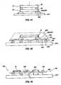
- FIG. 1is a perspective view of an exemplary embodiment of chip-scale package with castellated contact pads
- FIG. 2is a cross-section taken along line 2 - 2 of FIG. 1 ;
- FIGS. 3 through 14are cross-sectional representations of an exemplary method for forming the chip-scale package shown in FIGS. 1 and 2 ;
- FIGS. 4A through 9Aare cross-sectional representations showing a variation of the method depicted in FIGS. 4 through 14 ;
- FIG. 15is perspective view of another exemplary embodiment of chip-scale package that includes a sensor/emitter-type semiconductor device, as well as castellated contact pads positioned about the outer periphery thereof;
- FIG. 16is a cross-section taken along line 16 - 16 of FIG. 15 ;
- FIGS. 17 through 28are cross-sectional representations that show an exemplary process for forming chip-scale packages of the type illustrated in FIGS. 15 and 16 ;
- FIG. 29is a cross-sectional representation of a variation of the chip-scale package shown in FIG. 15 , in which an optically transparent lid is disposed over a sensing/emission area of the semiconductor device includes chamfered edges;
- FIGS. 30 through 35are cross-sectional representations that depict exemplary processes that may be used in the formation of chip-scale packages of the type shown in FIG. 29 ;
- FIGS. 36 through 40are cross-sectional representations illustrating various manners in which a chip-scale package according to the present invention may be electrically connected to another semiconductor device component or other electronic component;
- FIG. 41is a side view depicting an exemplary stacked assembly that includes chip-scale packages according to the present invention.
- FIG. 42is a cross-sectional representation of an exemplary packaged chip-scale package of the present invention, which includes a chip-scale package, a circuit board for reconfiguring the connection pattern of the chip-scale package, and an encapsulant material over the chip-scale package; and
- FIG. 43is a schematic representation of a multi-chip module that includes several semiconductor devices, including a chip-scale package that incorporates teachings of the present invention.
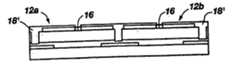
- Chip-scale package 10includes a semiconductor device 12 , a redistribution layer 20 over an active surface 13 thereof, and contact pads 30 that extend from redistribution layer 20 , around an outer peripheral edge 15 (also referred to herein as “outer periphery 15”) of semiconductor device 12 , and onto a back side 14 of semiconductor device 12 .
- each contact pad 30includes an upper section 32 , a peripheral section 34 , and a lower section 36 (see FIG. 2 ).
- contact pads 30are located adjacent to an outer peripheral edge 15 of semiconductor device 12 and, thus, at an outer peripheral edge 15 ′ of chip-scale package 10 , they impart chip-scale package 10 with a somewhat castellated appearance and, thus, are also referred to herein as “castellated contacts.”
- Semiconductor device 12includes bond pads 16 on active surface 13 thereof. Bond pads 16 are arranged substantially linearly along a centerline 17 of semiconductor device 12 , although semiconductor devices with other bond pad arrangements, or “footprints,” may also be used in chip-scale packages that incorporate teachings of the present invention.
- semiconductor device 12may comprise a memory device, such as a dynamic random access memory (DRAM), a static random access memory (SRAM), a programmable memory (PROM), an electrically erasable programmable memory (EEPROM), or the like.
- semiconductor device 12may comprise a so-called “microprocessor” or “microcontroller.”
- a dielectric layer 18is disposed on active surface 13 of semiconductor device 12 to protect the same and to electrically isolate active surface 13 from circuitry of redistribution layer 20 .
- dielectric layer 18may be configured to prevent electrical interference between signals transmitted along the integrated circuitry (not shown) of semiconductor device 12 and those transmitted along the circuitry of redistribution layer 20 .
- dielectric layer 18may be configured to prevent alpha particles, which are known to cause dissipation of stored charges within memory cells, from penetrating therethrough to the memory cells, if any, of the underlying semiconductor device 12 .
- the material from which dielectric layer 18 is formed, as well as the thickness thereofmay contribute to the characteristics thereof.
- Dielectric layer 18Materials that are suitable for use as dielectric layer 18 include, but are not limited to polyimides, silicon oxides, silicon nitrides, silicon oxynitrides, and the like.
- Dielectric layer 18includes apertures 19 formed therethrough, through which bond pads 16 of semiconductor device 12 are exposed.
- Redistribution layer 20includes a plurality of circuits 22 .
- Each circuit 22communicates with a corresponding bond pad 16 of semiconductor device 12 and extends laterally to and communicates with a corresponding contact pad 30 , adjacent to outer periphery 15 of semiconductor device 12 .
- chip-scale package 10may include a protective layer 40 over redistribution layer 20 .
- protective layer 40comprises a material which is electrically insulative and which may prevent alpha particles from penetrating through to the underlying semiconductor device 12 .
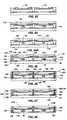
- FIGS. 3 through 14an exemplary embodiment of a method for fabricating chip-scale package 10 is shown.
- semiconductor substrate 11on which a plurality of semiconductor devices 12 (semiconductor devices 12 a , 12 b being shown) are carried may be provided.
- semiconductor substrate 11may comprise a full or partial wafer of semiconductive material (e.g., silicon, gallium arsenide, indium phosphide, etc.), a so-called silicon-on-insulator (SOI) type substrate (e.g., silicon-on-ceramic (SOC), silicon-on-glass (SOG), silicon-on-sapphire (SOS), etc.), or a single-device or multiple-device section of any of the foregoing substrates.
- SOIsilicon-on-insulator
- FIG. 4depicts a sacrificial substrate 50 that has dimensions which are substantially the same as or larger than the corresponding dimensions of semiconductor substrate 11 ( FIG. 3 ).
- a precursor pad 36 ′which is also referred to herein as a “conductive element,” which is a precursor of lower section 36 of each contact pad 30 ( FIGS. 1 and 2 ), is formed on an upper, or active, surface 52 of sacrificial substrate 50 .
- the lowermost portion of each precursor pad 36 ′i.e., that which is located adjacent surface 52
- each precursor pad 36 ′may include one or more sublayers of conductive material.
- Each conductive material layer or sublayermay be formed by known processes, such as by one or more of physical vapor deposition (PVD) (e.g., sputtering), chemical vapor deposition (CVD), electrolytic plating, electroless plating, immersion plating, or the like.
- PVDphysical vapor deposition
- CVDchemical vapor deposition
- electrolytic platingelectroless plating
- immersion platingimmersion plating
- one or more sublayers of each precursor pad 36 ′may be patterned, as known in the art (e.g., by use of mask and etch processes).
- a lowermost sublayer of conductive materialis formed by PVD or CVD processes
- that sublayermay be patterned prior to the formation of additional sublayers of conductive material thereover by electrolytic, electroless, or immersion plating processes.
- patterningmay be effected to form precursor pads 36 ′ after all of the sublayers have been formed or following each set of consecutive PVD or CVD processes.
- a centerline 37 through each precursor pad 36 ′is aligned between adjacent semiconductor devices 12 a and 12 b carried by semiconductor substrate 11 (i.e., with a scribe line S, or “street,” thereof). Accordingly, half 36 a ′ of precursor pad 36 ′ will be located beneath and positioned adjacent to an outer periphery 15 a of a first semiconductor device 12 a , while the other half 36 b ′ of precursor pad 36 ′ will be positioned beneath and adjacent to an outer periphery 15 b of an adjacent semiconductor device 12 b.
- discrete lower sections 36 a and 36 b of contact pads 30may be preformed on surface 52 of sacrificial substrate 50 , as known in the art.
- Discrete lower sections 36 a and 36 bmay, as depicted, have chamfered edges 37 .
- Such chamfering of edges 37 of discrete lower sections 36 a and 36 bmay provide a larger surface area than that provided by squared edges, ensuring that subsequently fabricated conductive structures will make adequate electrical contact to discrete lower sections 36 a and 36 b .
- discrete lower sections 36 a and 36 bhave chamfered edges 37 may facilitate the formation of chip-scale packages 10 ( FIGS. 1 and 2 ) from semiconductor substrates 11 ( FIG. 3 ) with relatively narrow streets S.
- discrete lowered sections 36 a and 36 b with squared edges 37are also within the scope of the present invention.
- a back side 14 ′ of semiconductor substrate 11which is common to back sides 14 of the semiconductor devices 12 that are carried by semiconductor substrate 11 , is positioned adjacent to surface 52 of sacrificial substrate 50 .
- semiconductor substrate 11is positioned in this manner, semiconductor devices 12 which are carried thereby are aligned with corresponding precursor pads 36 ′ ( FIG. 5 ) or between corresponding discrete lower sections 36 a , 36 b ( FIG. 5A ) on surface 52 of sacrificial substrate 50 .
- a bonding agent 54may be used to bond back side 14 ′ of semiconductor substrate 11 to surface 52 of sacrificial substrate 50 . Accordingly, bonding agent 54 may be applied to back side 14 ′, to surface 52 , or to both back side 14 ′ and surface 52 .
- known spin-on, spray-on, screen printing, and other application techniquesmay be used to apply bonding agent 54 .
- Bonding agent 54may comprise an electrically insulative material. Thus, bonding agent 54 may subsequently form a dielectric layer on back side 14 of semiconductor device 12 of the resulting chip-scale package 10 , as well as electrically isolate precursor pads 36 ′ from back side 14 of each semiconductor device 12 . Additionally, it is currently preferred that the adhesive material which is employed comprise a material that will apply little or no stress to semiconductor substrate 11 and sacrificial substrate 50 , or “low stress” material, thereby reducing the likelihood that either semiconductor substrate 11 or sacrificial substrate 50 will be damaged as chip-scale packages 10 are being formed. For example, and not to limit the scope of the present invention, bonding agent 54 may comprise an adhesive material.
- bonding agent 54may be stable at elevated temperatures, under reduced pressures (e.g., in a vacuum), when exposed to chemical environments, or other conditions to which bonding agent 54 will be exposed during downstream processes (e.g., fabrication of redistribution layers (RDLs).
- bonding agent 54may comprise a material that will not outgas at any temperature, particularly the temperatures to which it will be exposed during fabrication of chip-scale packages 10 and operation of semiconductor devices 12 thereof.
- Exemplary materials that may be used as bonding agent 54include, without limitation, any type of curable adhesive material that meets the specifications required for packaging semiconductor device components, such as thermoset adhesive materials, polyimides, and the like.
- adjacent semiconductor devices 12 a , 12 bare partially separated from one another, or singulated, along a street or scribe line S ( FIG. 5 ) therebetween, as depicted in FIGS. 6 and 6 A.
- separation or singulationmay be effected as known in the art.
- a wafer saw of a known typemay be employed.
- other known separation techniquese.g., laser cutting or machining techniques, mask and etch processes, etc.
- Cut lines 56are particularly useful when strict control over the width and depth of cut lines 56 is desired, such as when semiconductor substrate 11 includes narrow streets S between adjacent semiconductor devices 12 .
- the partial separationresults in cut lines 56 .
- Cut lines 56may extend a depth which is substantially the same as the thickness of semiconductor substrate 11 . As depicted, cut lines 56 do not extend completely through precursor pads 36 ′.
- a dielectric layer 18 ′which comprises electrically insulative material, is disposed on semiconductor substrate 11 and substantially fills cut lines 56 .
- the electrically insulative material of dielectric layer 18 ′may, by way of example only, comprise a polymer, such as a photoimageable material (e.g., photoresist, photoimageable polyimide, etc.). If such a polymer is used, it may be applied to semiconductor substrate 11 by known processes, such as by spin-on techniques, use of a doctor blade, screen printing processes, or the like.
- bond pads 16 of each semiconductor device 12 a , 12 bare exposed through dielectric layer 18 ′.
- dielectric layer 18 ′is formed from a photoimageable material, known photoimaging processes may be used. For example, if a photoimageable polyimide is employed, selected regions of uncured polyimide may be exposed to an appropriate wavelength of radiation and uncured material subsequently removed to expose bond pads 16 .
- a photoresistis employed as the electrically insulative material of dielectric layer 18 ′, selected regions of the photoresist, depending, of course, upon whether the photoresist is a negative tone resist or positive tone resist, may be exposed to radiation of an appropriate wavelength, then chemically developed, as known in the art.
- cut lines 58are formed between adjacent semiconductor devices 12 a , 12 b .
- cut lines 58may be formed by use of a wafer saw, laser cutting or machining techinques, mask and etch processes, or otherwise, as known in the art and suitable for use with the type of material from which dielectric layer 18 ′ is formed. Again, the use of laser cutting techniques is particularly desirable when the formation of relatively narrow cut lines 58 of particular depth is desired.
- Cut lines 58which are thinner or narrower than cut lines 56 , extend through the electrically insulative material of dielectric layer 18 ′, which is located between adjacent semiconductor devices 12 a and 12 b , leaving a peripheral dielectric coating 60 of the electrically insulative material on outer periphery 15 a , 15 b of semiconductor devices 12 a and 12 b . Also, cut lines 58 extend into and substantially through precursor pads 36 ′ exposing at least one edge 38 of the resulting lower section 36 of contact pad 30 ( FIGS. 1 and 2 ).
- cut lines 58do not extend into sacrificial substrate 50 .
- each precursor pad 36 ′is severed into two lower sections 36 of contact pads 30 , each corresponding to the semiconductor device 12 a , 12 b beneath which it is located.
- cut lines 58extend to discrete lower sections 36 a and 36 b , exposing edges 37 thereof.
- dielectric layer 18 ′is severed into a plurality of dielectric layers 18 , one for each semiconductor device 12 a , 12 b.
- a conductive layer 62which may include one or more metal sublayers, is deposited or otherwise disposed on semiconductor substrate 11 .
- conductive layer 62substantially overlies dielectric layers 18 , as well as peripheral dielectric coatings 60 .
- Conductive layer 62also contacts and, thus, electrically communicates with the exposed edges 38 of lower sections 36 of contact pads 30 and the exposed bond pads 16 ( FIGS. 1 and 2 ).
- Known processessuch as PVD or CVD processes, may be used to form at least a base portion of conductive layer 62 , while these or other techniques, such as electrolytic, electroless, or immersion plating processes, may be used to form subsequent sublayers (not shown) of conductive layer 62 .
- FIG. 11illustrates patterning of conductive layer 62 to form circuits 22 of redistribution layer 20 ( FIGS. 1 and 2 ), as well as contact pads 30 .
- Known processessuch as mask and etch techniques, may be used to form circuits 22 and upper sections 32 of contact pads 30 .
- peripheral sections 34are formed that communicate with upper sections 32 of the corresponding contact pads 30 , as well as with lower sections 36 thereof.
- Upper sections 32 and their corresponding lower sections 36may be located at substantially the same positions on opposite surfaces (i.e., active surface 13 and back side 14 , respectively) of semiconductor device 12 .
- a protective layer 40may be formed over redistribution layer 20 of each semiconductor device 12 a , 12 b , as shown in FIG. 12 .
- Protective layer 40is formed by applying a layer 40 ′ of electrically insulative material over semiconductor substrate 11 .
- the electrically insulative material of layer 40 ′may, by way of example only, comprise a polymer, such as a photoimageable polymer (e.g., a photoimageable polyimide, photoresist, etc.). If such a polymer is used, it may be applied to semiconductor substrate 11 by known processes, such as by spin-on techniques, use of a doctor blade, screen printing processes, or the like.
- upper and peripheral sections 32 and 34 of contact pads 30are exposed through layer 40 ′.
- layer 40 ′is formed from a photoimageable material, known photoimaging processes may be used. For example, if a photoimageable polyimide is employed, selected regions of uncured polyimide may be exposed to an appropriate wavelength of radiation and uncured material subsequently removed to expose contact pads 30 . As another example, if a photoresist is employed as the electrically insulative material of layer 40 ′, selected regions of the photoresist, depending, of course, upon whether the photoresist is a negative tone resist or positive tone resist, may be exposed to radiation of an appropriate wavelength, then chemically developed, as known in the art.
- one or more layers of UBM or BLMmay be formed, as known in the art (e.g., by electrolytic, electroless, or immersion plating techniques), on exposed portions of each contact pad 30 (i.e., upper section 32 and peripheral section 34 ).
- UBM or BLMwill prevent the material of contact pads 30 from oxidizing and facilitate adhesion of intermediate conductive elements, such as bond wires, solder bumps, or the like, thereto.
- the sections of contact pads 30 that are coated in this mannermay be recessed beneath the outer surface of protective layer 40 , extend substantially therethrough, or protrude therefrom. If UBM or BLM is formed on any section of contact pads 30 , such a coating may be formed before or after the formation of protective layer 40 .
- adjacent chip-scale packages 10 a , 10 b , etc.may be separated, or singulated, from one another by known processes.
- semiconductor substrate 11has already been severed to partially physically separate adjacent semiconductor devices 12 a and 12 b from one another. Accordingly, semiconductor devices 12 a and 12 b may be completely separated from one another and lower sections 36 of contact pads 30 exposed by removing sacrificial substrate 50 ( FIGS. 4 and 5 ) from each chip-scale package 10 a , 10 b , etc.
- known backgrinding processeswhich have been conventionally employed to reduce the thicknesses of semiconductor substrates following the fabrication of semiconductor devices thereon, may be used to substantially remove sacrificial substrate 50 from each chip-scale package 10 a , 10 b , etc.
- known etching processeswhich are, of course, suitable for use with the material or materials of sacrificial substrate 50 , may be employed to remove sacrificial substrate 50 .
- lower sections 36may be exposed by use of such a technique, with bonding agent 54 remaining on and electrically insulating back side 14 of each semiconductor device 12 a , 12 b , etc.
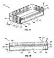
- Chip-scale package 110includes a sensor-type semiconductor device 112 , such as a CCD or other photocell, or a display-type device, such as an LED, a field emission device, or another emission device.
- a sensor-type semiconductor device 112such as a CCD or other photocell
- a display-type devicesuch as an LED, a field emission device, or another emission device.
- semiconductor device 112includes a sensing/emission area 170 which is exposed to an active surface 113 thereof. Additionally, to protect sensing/emission area 170 , chip-scale package 110 includes an optically transparent lid 172 over at least a portion of sensing/emission area or region 170 . Semiconductor device 112 also includes bond pads 116 on active surface 113 thereof, positioned between sensing/emission area 170 and outer peripheral edge 115 (also referred to as “outer periphery 115”).
- Chip-scale package 110further includes a redistribution layer 120 over active surface 113 of semiconductor device 112 , as well as contact pads 130 that extend from redistribution layer 120 , around the outer peripheral edge 115 of semiconductor device 112 , and onto a back side 114 of semiconductor device 112 .
- each contact pad 130includes an upper section 132 , a peripheral section 134 , and a lower section 136 (see FIG. 16 ).
- Contact pads 130are referred to herein as “castellated contacts” since they are located adjacent to an outer peripheral edge 115 of semiconductor device 112 and, thus, at an outer peripheral edge 115 of chip-scale package 110 and impart chip-scale package 110 with a somewhat castellated appearance.
- a dielectric layer 118is disposed on active surface 113 of semiconductor device 112 , laterally adjacent to optically transparent lid 172 , to protect active surface 113 and to prevent electrical interference, or “crosstalk,” between integrated circuitry of semiconductor device 112 and circuits 122 of redistribution layer 120 .
- Dielectric layer 118may also be configured to prevent alpha particles from penetrating therethrough to any memory cells or other charge-retaining areas of the underlying semiconductor device 112 .
- the material from which dielectric layer 118 is formed, as well as the thickness thereofmay contribute to the characteristics thereof. Materials that are suitable for use as dielectric layer 118 include, but are not limited to polyimides, silicon oxides, silicon nitrides, silicon oxynitrides, and the like. Bond pads 116 of semiconductor device 112 are exposed through dielectric layer 118 by way of apertures 119 formed therethrough.
- Redistribution layer 120includes upper sections 132 of contact pads 130 .
- Redistribution layer 120may also include a plurality of circuits 122 that extend from bond pads 116 to upper portions 132 of corresponding contact pads 130 .
- Chip-scale package 110may also include a protective layer (not shown) over redistribution layer 120 .
- the protective layercomprises a material which is electrically insulative and which may prevent alpha particles from penetrating through to the underlying semiconductor device 112 .
- FIGS. 17 through 28depict an exemplary process for packaging semiconductor devices 112 and, thus, for forming chip-scale packages 110 including the same.
- semiconductor substrate 111is provided.
- semiconductor substrate 111may comprise a full or partial wafer of semiconductive material, an SOI-type substrate, or a single-device or multiple-device section of any of the foregoing substrates.
- a temporary protective layer 180may be formed over sensing/emission region 170 of each semiconductor device 112 .
- Temporary protective layer 180may prevent contamination of sensing/emission region 170 while processes that must be conducted prior to the placement of an optically transparent lid 172 ( FIGS. 15 and 16 ) thereover are effected.
- Temporary protective layer 180may be formed by applying a layer of photoresist to active surface 113 (e.g., by spin-on processes, use of a doctor blade, screen printing, etc.), then exposing and developing selected regions of the layer of photoresist.
- a layer of photoresiste.g., by spin-on processes, use of a doctor blade, screen printing, etc.
- suitable processese.g., spin-on processes for photoimageable materials, or screen printing for nonphotoimageable materials
- semiconductor substrate 111is secured to a sacrificial substrate 50 , such as that shown in FIG. 4 .
- a bonding agent 54 of a known typemay be applied to a surface 52 of sacrificial substrate 50 , a back side 114 ′ of semiconductor substrate 111 , or both.
- the bonding agent 54is applied in such a way (e.g., in a quantity) that will electrically isolate precursor pads 136 ′ on surface 52 of sacrificial substrate 50 from back side 114 ′ of semiconductor substrate 111 .
- Back side 114 ′is positioned adjacent to and in contact with surface 52 , with semiconductor devices 112 that are carried by semiconductor substrate 111 in alignment over corresponding portions of precursor pads 136 ′.
- adjacent semiconductor devices 112are partially separated from one another, or singulated, along a street or scribe line S therebetween, as depicted in FIG. 19 .
- separation or singulationmay be effected as known in the art.
- a wafer saw of a known typemay be employed.
- other known separation techniquese.g., mask and etch processes, laser machining techniques, etc.
- the partial separationresults in cut lines 156 , which may extend a depth which is substantially the same as the thickness of semiconductor substrate 111 .
- a dielectric layer 118 ′which comprises electrically insulative material, is applied to or formed on semiconductor substrate 111 in such a way as to substantially fill cut lines 156 .
- the electrically insulative material of dielectric layer 118 ′will withstand processes (e.g., resist strip processes) that are to be subsequently employed to remove the material of temporary protective layer 180 .
- dielectric layer 118 ′may comprise a polymer, such as a photoimageable material (e.g., photoresist, photoimageable polyimide, etc.).
- a polymermay be applied to semiconductor substrate 111 by known processes, such as by spin-on techniques, use of a doctor blade, screen printing processes, or the like.
- spin-on-glass or another suitable, nonpolymeric, electrically insulative materialmay be used to form dielectric layer 118 ′.
- dielectric layer 118 ′is patterned in such a way that apertures 119 are formed therethrough, over bond pads 116 of each semiconductor device 112 . Thus, bond pads 116 are exposed through apertures 119 of dielectric layer 118 ′.
- Known processessuch as those mentioned above in reference to FIG. 8 , may be used to pattern dielectric layer 118 ′.
- a conductive layer 162is formed over dielectric layer 118 ′ and in apertures 119 .
- conductive layer 162may include a single layer or a plurality of sublayers (not shown). If conductive layer 162 includes a single layer, known processes, such as PVD or CVD processes, may be used to form the same. If conductive layer 162 includes a plurality of sublayers, the lowermost sublayer may be formed, for example, by PVD or CVD processes, while a variety of techniques, including, without limitation, PVD, CVD, electrolytic plating, electroless plating, and immersion plating processes, may be used to form the remaining sublayers.
- conductive layer 162may be patterned to form upper precursor pads 132 ′, which are precursors to upper sections 132 of contact pads 130 ( FIGS. 15 and 16 ), that extend across the boundary between adjacent semiconductor devices 112 a and 112 b .
- conductive layer 162may be patterned to form discrete upper sections 132 of contact pads 130 , with a peripheral edge 133 of each upper section 132 being located substantially directly above and extending along substantially the same plane as outer periphery 115 of its corresponding semiconductor device 112 .
- circuits 122may be formed so as to extend laterally from the locations of bond pads 116 to their corresponding upper precursor pads 132 ′ ( FIG. 22 ) or upper sections 132 ( FIG. 22A ) of contact pads 130 ( FIGS. 15 and 16 ).
- Precursor pads 132 ′, upper sections 132 , and circuits 122may be formed by known processes, such as mask and etch techniques.
- temporary protective layers 180 and regions of dielectric layer 118 ′ that remain thereovermay be removed to expose the underlying sensing/emission region 170 , as shown in FIG. 23 .
- resist strip techniquesthat are suitable for use with that type of photoresist may be used to substantially remove the same.
- other, suitable processese.g., use of etchants, irradiation techniques, etc.
- the removal of temporary protective layer 180be effected without substantially removing dielectric layer 118 ′.
- a preformed optically transparent lid 172 ′may be positioned over semiconductor substrate 111 and secured thereto with a quantity of optical grade adhesive 174 .
- optically transparent lid 172 ′may cover a plurality of semiconductor devices 112 and, thus, extend over the boundaries between adjacent semiconductor devices 112 a , 112 b .
- optically transparent lid 172 ′may have substantially the same lateral dimensions as semiconductor substrate 111 .
- a quantity of an optical grade adhesive 174 of a known typemay be applied to one or both of optically transparent lid 172 ′ and semiconductor substrate 111 by known techniques, such as use of a dispense needle, screen printing, spin-on processes, or the like.
- a plurality of individual optically transparent lids 172may be positioned over sensing/emission area 170 of each semiconductor device 112 and secured to semiconductor device 112 with an optical grade adhesive 174 , as known in the art and as depicted in FIG. 24A .
- cut lines 158are formed along the streets between adjacent semiconductor devices 112 a and 112 b .
- each cut line 158is aligned with a corresponding cut line 156 and is thinner, or narrower, than its corresponding cut line 156 .
- a peripheral dielectric coating 160 of the material of dielectric layer 118 ′remains on outer periphery 115 of each semiconductor device 112 a , 112 b , etc., so as to electrically insulate the same from a subsequently formed peripheral section 134 of each contact pad 130 ( FIGS. 15 and 16 ).
- each cut line 158exposes a peripheral edge 133 of upper section 132 of each contact pad 130 , as well as peripheral edge 137 of lower section 136 of each contact pad 130 .
- Cut lines 158are formed by a technique (e.g., with a wafer saw, by laser ablation, by etching processes, etc.) which is suitable for removing the material of dielectric layer 118 ′ and, if a single optically transparent lid 172 ′ has been employed, for removing the material of optically transparent lid 172 ′.
- a techniquee.g., with a wafer saw, by laser ablation, by etching processes, etc.
- the formation of cut lines 158results in the severing of optically transparent lid 172 ′ into a plurality of individual optically transparent lids 172 , with one optically transparent lid 172 being located over each semiconductor device 112 a , 112 b.
- cut lines 158should also be suitable for removing the material of such precursor pads 132 ′, 136 ′.
- precursor pads 132 ′ or 136 ′are severed during the formation of a cut line 158 , they are bisected or otherwise split into upper sections 132 a , 132 b (collectively, upper sections 132 ) or lower sections 136 a , 136 b (collectively, lower sections 136 ) that are located on active surface 113 or back side 114 of adjacent semiconductor devices 1 12 a , 112 b , respectively, with peripheral edges 133 , 137 being formed at each edge of that cut line 158 .
- each cut line 158extends at least to surface 52 of sacrificial substrate 50 .
- FIG. 26depicts the disposal of a layer 163 ′ of sacrificial material over semiconductor devices 112 (e.g., on optically transparent lids 172 and any other structures that are exposed laterally beyond optically transparent lids 172 ).
- the sacrificial material of layer 163 ′may comprise a photoresist or another photoimageable material in an uncured state.
- Such a materialmay be applied to optically transparent lids 172 and introduced into cut lines 158 by known processes, such as by spin-on techniques, use of a doctor blade, or the like.
- a photoresistWhen a photoresist is used, known patterning processes (e.g., selective exposure to radiation, then developing) may be used to selectively cure and form a sacrificial layer 163 from the uncured photoimageable material of layer 163 ′. Uncured portions of layer 163 ′ are then removed from semiconductor substrate 111 (e.g., from cut lines 158 ), as known in the art (e.g., by known cleaning processes). As depicted, sacrificial layer 163 is located over semiconductor devices 112 , but does not extend into cut lines 158 .
- known patterning processese.g., selective exposure to radiation, then developing
- an uncured polymer which is not photoimageablemay be used to form layer 163 ′.
- a materialmay be applied over selected regions of semiconductor devices 112 (e.g., on optically transparent lids 172 thereof, but not within cut lines 158 ), such as by use of screen printing techniques, selective deposition processes (e.g., by use of a two-dimensional, ink jet-type printer), or the like.
- the materialmay then be permitted to harden (in the case of thermoplastic materials) or cure, or caused to cure (e.g., by exposure to heat, pressure, radiation of an appropriate wavelength, a chemical catalyst, etc.), as known in the art, to form sacrificial layer 163 .
- a conductive layer 164may be formed thereover.
- conductive layer 164may include a single layer or a plurality of sublayers of conductive material.
- PVD or CVD techniquesmay be used to form all of conductive layer 164 or a lowermost sublayer thereof, while PVD, CVD, electrolytic plating, electroless plating, or immersion plating processes may be used to form any sublayers of conductive layer 164 that are located over the lowermost sublayer thereof.
- conductive layer 164overlies semiconductor devices 112 a , 112 b (being located over optically transparent lids 172 that are disposed thereover), as well as lines peripheral dielectric coatings 160 , which form the lateral surfaces of each cut line 158 . Additionally, peripheral edges 133 of upper sections 132 of contact pads 130 ( FIGS. 15 and 16 ) and edges 137 of lower sections 136 of contact pads 130 , which are located within cut lines 158 , are contacted by portions 166 of conductive layer 164 that are located within cut lines 158 .
- sacrificial layer 163may be removed by processes that are suitable for use with the material thereof.
- the portions 165 ( FIG. 26 ) of conductive layer 164 ( FIG. 26 ) that overlie sacrificial layer 163are “lifted-off” by the process or processes that are used to remove sacrificial layer 163 .
- sacrificial layer 163comprises a photoresist material
- a resist strip which is able to remove that photoresist materialmay be used to substantially remove sacrificial layer 163 , as well as to lift portions 165 of conductive layer 164 that previously overlaid sacrificial layer 163 off of semiconductor substrate 111 and away from semiconductor devices 112 that are carried thereby.
- FIG. 27illustrates, portions 166 of conductive layer 164 that are located within cut lines 158 remain therein following completion of the “lift-off” process.
- portions 166 of conductive layer 164 that are located within cut lines 158may be patterned, by known processes (e.g., mask and etch techniques), to form peripheral sections 134 of contact pads 130 ( FIG. 27 ), which extend between their corresponding upper sections 132 and lower sections 136 .
- Such patterning of portions 166may be effected prior to the “lift-off” process, in which case sacrificial layer 163 ( FIG. 26 ) should be formed from a material that may be removed without substantially removing the material of peripheral dielectric coatings 160 .
- portions 166may be effected following the “lift-off” process, in which case the material of portions 166 shields the material of peripheral dielectric coatings 160 during the removal of sacrificial layer 163 and the resulting “lift-off” of portions 165 ( FIG. 26 ) of conductive layer 164 ( FIG. 26 ).
- UBM or BLMmay be formed, as known in the art (e.g., by electrolytic, electroless, or immersion plating techniques) on exposed portions of each contact pad 130 (e.g., peripheral section 134 ).
- Such UBM or BLMwill prevent contact pads 130 from oxidizing and facilitate adhesion of intermediate conductive elements, such as bond wires, solder bumps, or the like, thereto.
- adjacent chip-scale packages 110 a , 110 b , etc.may be separated, or singulated, from one another by known processes.
- semiconductor substrate 111has already been severed to partially physically separate adjacent semiconductor devices 112 a and 112 b from one another. Accordingly, semiconductor devices 112 a and 112 b may be completely separated from one another and lower sections 136 of contact pads 130 exposed by removing sacrificial substrate 50 ( FIG. 18 ) from each chip-scale package 110 a , 110 b , etc.
- known backgrinding processesmay be used to substantially remove sacrificial substrate 50 from each chip-scale package 110 a , 110 b , etc.
- known etching processeswhich are, of course, suitable for use with the material or materials of sacrificial substrate 50 , may be employed to remove sacrificial substrate 50 .
- lower sections 136may be exposed by use of such a technique, with bonding agent 54 remaining on and electrically insulating back side 114 of each semiconductor device 112 a , 112 b , etc.
- Chip-scale package 110differs from chip-scale package 110 in that optically transparent lid 172 ′′ includes bevels or chamfers 178 ′′ at peripheral edges 175 ′′ thereof.
- a plurality of chip-scale packages 110 ′′may be formed by repeating the processes that have been described with reference to FIGS. 17-24A .
- a bevel cut 176may be made at locations of each optically transparent lid 172 ′′, 172 ′, 172 that is positioned over and laterally adjacent to outer peripheral edges 115 of semiconductor devices 112 .
- Such a bevel cut 176may be formed, for example, by use of a saw (e.g., a wafer saw) having a beveled edge on each side thereof, by way of isotropic etching processes, or otherwise, as known in the art.
- a sawe.g., a wafer saw
- a sacrificial layer 163may be formed over optically transparent lids 172 ′′, such as in the manner that has been described herein with reference to FIG. 26 . It is currently preferred that sacrificial layer 163 overlie the bevels 177 a and 177 b at each side of bevel cut 176 .
- a cut line 158 ′′may be formed between each pair of adjacent semiconductor devices 112 a and 112 b , as described in reference to FIG. 25 .
- each cut line 158 ′′is aligned with and substantially centered along a corresponding bevel cut 176 .
- a conductive layer 164is formed over sacrificial layer 163 and on peripheral dielectric coating 160 at each lateral edge of each cut line 158 ′′.
- conductive layer 164may be formed by the processes that are described herein with reference to FIG. 26 .
- bevel cuts 176may improve the deposition of conductive layer 164 on peripheral dielectric coatings 160 within cut line 158 ′′.
- edges 133 ′ of upper sections 132 of contact pads 130 ( FIGS. 15 and 16 ) and edges 137 of lower sections 136 of contact pads 130which are located within cut lines 158 ′′, are contacted by portions 166 of conductive layer 164 that are located within cut lines 158 ′′.
- portions 165 ( FIG. 33 ) of conductive layer 164 ( FIG. 33 ) that overlie sacrificial layer 163may be removed, or “lifted-off,” by substantially removing sacrificial layer 163 .
- Sacrificial layer 163may be substantially removed, for example, by one of the processes that have been described in reference to FIG. 27 .
- sacrificial layer 163coats bevels 177 a and 177 b
- sacrificial layer 163also prevents the conductive material of portions 165 from remaining on peripheral edges 175 ′′ of optically transparent lid 172 ′′.
- Patterning of portions 166 of conductive layer 164 that reside within cut lines 158 ′′may be effected, as shown in FIG. 34 and as described herein with reference to FIG. 27 . Thereafter, as shown in FIG. 35 and as described with reference to FIG. 28 , sacrificial substrate 50 may be removed from semiconductor substrate 111 to completely separate chip-scale packages 110 a ′′, 10 b ′′, etc., from one another.
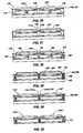
- FIGS. 36 through 38exemplary techniques for securing a chip-scale package 10 , 110 , 110 ′′ according to the present invention to a carrier substrate 210 (e.g., a circuit board) therefor are depicted.
- a carrier substrate 210e.g., a circuit board
- chip-scale package 10 , 110 , 110 ′′is positioned over carrier substrate 210 with a bottom surface 14 ′′ of chip-scale package 10 , 110 , 110 ′′ facing an upper surface 213 of carrier substrate 210 .
- Intermediate conductive elements 220 , 220 ′′which are respectively shown as being conductive balls (e.g., solder balls) and larger, nonspherical conductive structures, but which may alternatively comprise bumps, columns, pillars, or pins of solder, another metal, conductive or conductor-filled epoxy, or any other suitable conductive material, or which may comprise z-axis conductive elements of a film of anisotropic conductive film, are positioned between bottom surface 14 ′′ of chip-scale package 10 , 110 , 110 ′′ and upper surface 213 of carrier substrate 210 . As shown, intermediate conductive elements 220 extend between and contact lower sections 36 , 136 of contact pads 30 , 130 of chip-scale package 10 , 110 , 110 ′′ and corresponding terminals 230 of carrier substrate 210 .
- conductive ballse.g., solder balls
- nonspherical conductive structuresbut which may alternatively comprise bumps, columns, pillars, or pins of solder, another metal, conductive or conductor
- chip-scale package 10 , 110may be oriented face-down over surface 213 of carrier substrate 210 .
- bottom surface 14 ′′ of chip-scale package 10 , 110faces away from (i.e., in the same direction as) surface 213 of carrier substrate 210 .
- intermediate conductive elements 220 , 220 ′′are positioned between chip-scale package 10 , 110 and carrier substrate 210 and electrically connect upper sections 32 , 132 of contact pads 30 , 130 with corresponding terminals 230 .
- chip-scale package 10 , 110 , 110 ′′may be used to electrically connect chip-scale package 10 , 110 , 110 ′′ to a carrier substrate 210 ′ therefor in a face-up orientation, or to electrically connect chip-scale package 10 , 110 to carrier substrate 210 ′ in a face-down orientation.
- chip-scale package 10 , 110 , 110 ′′is positioned on a surface 213 ′ of carrier substrate 210 ′ within a boundary defined by terminals 230 ′ thereon.
- a peripheral section 34 , 134 of each contact pad 30 , 130 of chip-scale package 10 , 110 , 110 ′′is laterally aligned with a corresponding terminal 230 ′ of carrier substrate 210 ′.
- Intermediate conductive elements 220 ′which comprise bumps of conductive material, are disposed in a corner 232 formed at the junction between each peripheral section 34 , 134 and its corresponding terminal 230 ′.
- FIG. 41illustrates a stacked multi-chip module 310 , which includes a carrier substrate 210 and a plurality of chip-scale packages 10 according to the present invention that have been stacked relative to one another over carrier substrate 210 .
- Corresponding contact pads 30 of chip-scale packages 10are electrically connected to one another and to corresponding terminals 230 of carrier substrate 210 by way of intermediate conductive elements 220 , 220 ′′.
- FIG. 42depicts use of a chip-scale package 10 of the present invention with a redistribution carrier 250 of a type known in the art (e.g., a printed circuit board), which includes conductive traces 254 on a first side 252 thereof that redistribute the connection pattern provided by contacts 30 of chip-scale package 10 to another arrangement of terminals 256 on an opposite, second side 258 of redistribution carrier 250 .
- the arrangement of terminals 256 on redistribution carrier 250corresponds to the connection pattern of corresponding terminals 230 ′′ on a carrier substrate 210 ′′ to which chip-scale package 10 is to be electrically connected, as known in the art.
- Chip-scale package 10 and an adjacent surface of redistribution carrier 250may also be at least partially encapsulated within a packaging material 259 .
- FIG. 43depicts a semiconductor device assembly 320 which includes a carrier substrate 210 ′′′ with a multi-chip module 330 secured and electrically connected thereto.
- Multi-chip module 330includes a substrate 260 with at least one chip-scale package 10 and one or more other types of semiconductor device packages 340 , 342 , 344 thereon.
Landscapes
- Engineering & Computer Science (AREA)
- Microelectronics & Electronic Packaging (AREA)
- Power Engineering (AREA)
- Computer Hardware Design (AREA)
- Physics & Mathematics (AREA)
- Condensed Matter Physics & Semiconductors (AREA)
- General Physics & Mathematics (AREA)
- Manufacturing & Machinery (AREA)
- Ceramic Engineering (AREA)
- Internal Circuitry In Semiconductor Integrated Circuit Devices (AREA)
Abstract
Description
- 1. Field of the Invention
- The present invention relates generally to chip-scale packages and, more specifically, to chip-scale packages which include contact pads on both major surfaces thereof, as well as to methods for forming the chip-scale packages. In particular, the present invention relates to chip-scale packages that include castellated contact pads, which include surfaces, or sections, that are exposed at the outer peripheries of such packages, as well as sections that are exposed at both major surfaces of the packages.
- 2. Background of Related Art
- Conventional semiconductor device packages are typically multi-layered structures. A conventional semiconductor device package may include, for example, a bottom layer of encapsulant material, a carrier, a semiconductor die, and a top layer of encapsulant material. In addition to being located above and beneath the semiconductor die and carrier, the encapsulant material of a conventional semiconductor device package also laterally surrounds the semiconductor device and the carrier. In addition, a conventional semiconductor device package includes input/output elements to facilitate electrical connection of the semiconductor device thereof with external electronic components.
- Leads are an example of conventional input/output elements. Leads typically contribute to the dimensions of the footprint of a conventional semiconductor device package and, thus, consume an undesirably large amount of real estate upon a carrier substrate (e.g., a circuit board) to which the semiconductor device package is to be secured and electrically connected.
- Other examples of such input/output elements include pins, solder balls or other discrete conductive structures (e.g., bumps, balls, columns, etc.), which contribute to the height of a conventional semiconductor device package. When coupled with the thicknesses that conventional encapsulants and carriers impart to the overall thickness of a conventional semiconductor device package, the added heights of such discrete conductive structures may result in a semiconductor device package which will protrude an undesirably large distance from a carrier substrate to which it is secured and electrically connected.
- In order to keep up with the trend toward ever-decreasing the dimensions of electronic devices, various technologies have been developed to decrease the dimensions of packaged semiconductor devices. The result of many of these technologies is the so-called “chip-scale package” (CSP), a packaged semiconductor device with lateral dimensions that are roughly the same as (i.e., slightly larger than) the corresponding lateral dimensions of the semiconductor dice thereof.
- Due to the relatively small, semiconductor die-dependent, lateral dimensions of CSPs, they are often formed at the so-called “wafer-scale,” meaning that packaging occurs prior to severing the semiconductor devices from a wafer or other large-scale substrate. Packaging semiconductor devices at the wafer-scale avoids the difficulties that may otherwise be associated with handling such small components during chip-scale packaging thereof. Such wafer-scale packaging may include the formation of a redistribution layer (RDL), which may rearrange or effectively expand the connection pattern of bond pads on the active surface of the semiconductor device to a redistributed connection pattern which is more suitable for connection to a carrier substrate. Alternatively, one or more interposers may be secured over the active surfaces of the semiconductor devices that are carried by a wafer or other large-scale substrate and electrically connected to such semiconductor devices to redistribute the connection patterns thereof.
- Once the connection patterns of the semiconductor devices have been redistributed and either before or after the formation of a protective layer over the RDL or interposer, discrete conductive elements, such as balls, bumps, columns, or pins, may be secured to the redistributed bond pads of each CSP. These discrete conductive structures are typically arranged over the major surface in a so-called “grid array” connection pattern.
- As a consequence of the use of such discrete conductive structures, chip-scale package technology typically requires inversion of the CSP face-down over a carrier substrate therefor and alignment of the discrete conductive structures of the CSP with corresponding contacts (e.g., the terminals of a circuit board). Electrical connection of a semiconductor device to a carrier substrate in this manner is referred to in the art as “flip-chip” connection or “controlled-collapse chip connection” (C4). Of course, when the discrete conductive structures comprise pins, the electrical connection technique is referred to as a “pin connection.”
- When flip-chip or pin connection techniques are employed, the discrete conductive elements typically space the semiconductor device apart from the carrier substrate. This space may remain open or be filled with a so-called “underfill” material. Such spacing of a semiconductor device apart from a carrier substrate may therefore impart the assembly with an undesirably high profile.
- Moreover, these types of chip-scale packaging technologies typically do not permit the placement of a chip-scale package on a carrier substrate in a face-up orientation.
- Accordingly, there is a need for a packaging technology which results in chip-scale packages that may be secured to carrier substrates without requiring a significant amount of spacing between the chip-scale packages and the carrier substrate and that may be electrically connected to a carrier substrate in a face-up orientation.
- The present invention includes a chip-scale package with bond pads, or contact pads, that are positioned around the outer periphery thereof. Additionally, the contact pads may extend onto one or both major surfaces of the chip-scale package.
- An exemplary embodiment of a chip-scale package that incorporates teachings of the present invention includes a semiconductor device, a redistribution layer formed over an active surface of the semiconductor device and in electrical isolation therefrom, and contact pads with sections that are positioned adjacent to and in electrical isolation from the outer periphery of the semiconductor device and which communicate with corresponding bond pads of the semiconductor device through the redistribution layer. One or more of the contact pads may also include an upper or lower section, which is located adjacent to and may be substantially coplanar with a respective active surface or back side of the semiconductor device.
- The semiconductor device of such a chip-scale package may comprise a memory device or a processing device, or a sensor or display device. If a sensor or display device is included in a chip-scale package of the present invention, at least a sensing or emission area on the active surface thereof may be covered with an optically transparent lid.
- The present invention also includes methods for forming chip-scale packages that include contact pads on the outer peripheries thereof. These methods may be effected at a wafer-scale.
- As an example, a wafer or other large-scale substrate carrying a plurality of semiconductor devices, which is referred to herein as a “semiconductor substrate,” may be secured to a sacrificial, or “dummy,” substrate. The sacrificial substrate may include lower contact pad sections, which are referred to herein as “lower sections” for simplicity, or precursors thereto, which are referred to herein as “precursor pads.” These lower sections or precursor pads are positioned so as to align with corresponding semiconductor devices when the semiconductor substrate is secured to the sacrificial substrate.
- Insulative and redistribution layers are formed over the semiconductor devices by use of known processes. The results are circuit traces that communicate with bond pads and extend from the bond pads toward or to the outer periphery of the semiconductor device. If the contact pads of the chip-scale package under fabrication are to include upper sections, which are positioned adjacent to the active surface of the semiconductor device, the upper sections may also be formed during the fabrication of the redistribution layer, with at least some of the circuit traces extending to corresponding upper sections. The insulative and redistribution layers may be formed either before or after the semiconductor substrate is secured to the sacrificial substrate.
- Once the insulative and redistribution layers have been formed and the semiconductor substrate has been secured to the sacrificial substrate, the semiconductor devices are at least partially severed from one another. If the sacrificial substrate includes lower sections of contact pads, such severing may expose portions (e.g., edges or a surface) of the lower sections. If the sacrificial substrate includes precursor pads thereon, such severing may sever the precursor pads or expose a surface thereof.
- Next, the exposed, outer peripheral edges of the semiconductor devices are coated with an electrically insulative material. Such coating may be followed by a second cut. The result is a peripheral dielectric coating on each peripheral edge of each semiconductor device. At this point in the packaging process, the semiconductor devices that are carried by the semiconductor substrate are substantially separated from one another and are held in place relative to one another by way of the sacrificial substrate. In addition, the outer edges of any lower sections of contact pads are exposed.
- Each peripheral dielectric coating is subsequently coated with a layer of conductive material. The conductive material is then patterned to form the peripherally located contact pads or peripheral sections thereof. Of course, if the contact pads of the chip-scale package include upper or lower sections, such patterning is effected such that the peripheral section of each contact pad communicates with its corresponding upper or lower section.
- Thereafter, the sacrificial substrate is removed from the semiconductor substrate, with any lower sections of contact pads remaining in place. As the sacrificial substrate is removed, the chip-scale packages that have been formed are fully separated from one another.
- If the semiconductor devices that are to be packaged comprise sensor or emission devices, the packaging process may differ somewhat. In particular, in other embodiments of the method of the present invention, the sensing or emission areas on the active surfaces of such semiconductor devices are protected prior to both the singulation of the semiconductor devices from one another and the introduction of dielectric material between adjacent semiconductor devices. In addition, an optically transparent lid is placed over each sensing or emission area following the formation of a redistribution layer, but prior to cutting into the dielectric material between adjacent semiconductor devices to form the peripheral dielectric coatings on the peripheral edges of the semiconductor devices. Finally, a sacrificial layer is formed over the optically transparent lids and above other locations of the semiconductor devices but not on the peripheral dielectric coatings prior to the formation of a conductive layer over these structures. As such, conductive material may be removed from desired locations, such as the optically transparent lids and other locations over the active surfaces of the semiconductor devices, by known “lift-off” techniques, while remaining on the peripheral dielectric coatings.
- Of course, semiconductor device assemblies and electronic devices which include such chip-scale packages, as well as methods for forming such assemblies and electronic devices, are also within the scope of the present invention.
- Other features and advantages of the present invention will become apparent to those of ordinary skill in the art through consideration of the ensuing description, the accompanying drawings, and the appended claims.
- In the drawings, which depict exemplary embodiments of various aspects of the present invention:
FIG. 1 is a perspective view of an exemplary embodiment of chip-scale package with castellated contact pads;FIG. 2 is a cross-section taken along line2-2 ofFIG. 1 ;FIGS. 3 through 14 are cross-sectional representations of an exemplary method for forming the chip-scale package shown inFIGS. 1 and 2 ;FIGS. 4A through 9A are cross-sectional representations showing a variation of the method depicted inFIGS. 4 through 14 ;FIG. 15 is perspective view of another exemplary embodiment of chip-scale package that includes a sensor/emitter-type semiconductor device, as well as castellated contact pads positioned about the outer periphery thereof;FIG. 16 is a cross-section taken along line16-16 ofFIG. 15 ;FIGS. 17 through 28 are cross-sectional representations that show an exemplary process for forming chip-scale packages of the type illustrated inFIGS. 15 and 16 ;FIG. 29 is a cross-sectional representation of a variation of the chip-scale package shown inFIG. 15 , in which an optically transparent lid is disposed over a sensing/emission area of the semiconductor device includes chamfered edges;FIGS. 30 through 35 are cross-sectional representations that depict exemplary processes that may be used in the formation of chip-scale packages of the type shown inFIG. 29 ;FIGS. 36 through 40 are cross-sectional representations illustrating various manners in which a chip-scale package according to the present invention may be electrically connected to another semiconductor device component or other electronic component;FIG. 41 is a side view depicting an exemplary stacked assembly that includes chip-scale packages according to the present invention;FIG. 42 is a cross-sectional representation of an exemplary packaged chip-scale package of the present invention, which includes a chip-scale package, a circuit board for reconfiguring the connection pattern of the chip-scale package, and an encapsulant material over the chip-scale package; andFIG. 43 is a schematic representation of a multi-chip module that includes several semiconductor devices, including a chip-scale package that incorporates teachings of the present invention.- With reference to
FIGS. 1 and 2 , an exemplary embodiment of a chip-scale package 10 that incorporates teachings of the present invention is depicted. Chip-scale package 10 includes asemiconductor device 12, aredistribution layer 20 over anactive surface 13 thereof, andcontact pads 30 that extend fromredistribution layer 20, around an outer peripheral edge15 (also referred to herein as “outer periphery 15”) ofsemiconductor device 12, and onto aback side 14 ofsemiconductor device 12. Accordingly, eachcontact pad 30 includes anupper section 32, aperipheral section 34, and a lower section36 (seeFIG. 2 ). Ascontact pads 30 are located adjacent to an outerperipheral edge 15 ofsemiconductor device 12 and, thus, at an outerperipheral edge 15′ of chip-scale package 10, they impart chip-scale package 10 with a somewhat castellated appearance and, thus, are also referred to herein as “castellated contacts.” Semiconductor device 12 includesbond pads 16 onactive surface 13 thereof.Bond pads 16 are arranged substantially linearly along acenterline 17 ofsemiconductor device 12, although semiconductor devices with other bond pad arrangements, or “footprints,” may also be used in chip-scale packages that incorporate teachings of the present invention.- By way of example only,
semiconductor device 12 may comprise a memory device, such as a dynamic random access memory (DRAM), a static random access memory (SRAM), a programmable memory (PROM), an electrically erasable programmable memory (EEPROM), or the like. As another example,semiconductor device 12 may comprise a so-called “microprocessor” or “microcontroller.” - A
dielectric layer 18 is disposed onactive surface 13 ofsemiconductor device 12 to protect the same and to electrically isolateactive surface 13 from circuitry ofredistribution layer 20. By way of example only,dielectric layer 18 may be configured to prevent electrical interference between signals transmitted along the integrated circuitry (not shown) ofsemiconductor device 12 and those transmitted along the circuitry ofredistribution layer 20. Also,dielectric layer 18 may be configured to prevent alpha particles, which are known to cause dissipation of stored charges within memory cells, from penetrating therethrough to the memory cells, if any, of theunderlying semiconductor device 12. Of course, the material from whichdielectric layer 18 is formed, as well as the thickness thereof, may contribute to the characteristics thereof. Materials that are suitable for use asdielectric layer 18 include, but are not limited to polyimides, silicon oxides, silicon nitrides, silicon oxynitrides, and the like.Dielectric layer 18 includesapertures 19 formed therethrough, through whichbond pads 16 ofsemiconductor device 12 are exposed. Redistribution layer 20 includes a plurality ofcircuits 22. Eachcircuit 22 communicates with acorresponding bond pad 16 ofsemiconductor device 12 and extends laterally to and communicates with acorresponding contact pad 30, adjacent toouter periphery 15 ofsemiconductor device 12.- Additionally, chip-
scale package 10 may include aprotective layer 40 overredistribution layer 20. Likedielectric layer 18,protective layer 40 comprises a material which is electrically insulative and which may prevent alpha particles from penetrating through to theunderlying semiconductor device 12. - Turning now to
FIGS. 3 through 14 , an exemplary embodiment of a method for fabricating chip-scale package 10 is shown. - In
FIG. 3 , at least onesemiconductor device 12 is provided. As shown, asemiconductor substrate 11 on which a plurality of semiconductor devices12 (semiconductor devices semiconductor substrate 11 may comprise a full or partial wafer of semiconductive material (e.g., silicon, gallium arsenide, indium phosphide, etc.), a so-called silicon-on-insulator (SOI) type substrate (e.g., silicon-on-ceramic (SOC), silicon-on-glass (SOG), silicon-on-sapphire (SOS), etc.), or a single-device or multiple-device section of any of the foregoing substrates. FIG. 4 depicts asacrificial substrate 50 that has dimensions which are substantially the same as or larger than the corresponding dimensions of semiconductor substrate11 (FIG. 3 ). As shown, aprecursor pad 36′, which is also referred to herein as a “conductive element,” which is a precursor oflower section 36 of each contact pad30 (FIGS. 1 and 2 ), is formed on an upper, or active,surface 52 ofsacrificial substrate 50. The lowermost portion of eachprecursor pad 36′ (i.e., that which is located adjacent surface52) may include under-bump metallization (UBM) or bond-limiting metallurgy (BLM). Accordingly, eachprecursor pad 36′ may include one or more sublayers of conductive material.- Each conductive material layer or sublayer may be formed by known processes, such as by one or more of physical vapor deposition (PVD) (e.g., sputtering), chemical vapor deposition (CVD), electrolytic plating, electroless plating, immersion plating, or the like. Depending upon the deposition technique(s) that is (are) used, as well as the order of deposition processes, one or more sublayers of each
precursor pad 36′ may be patterned, as known in the art (e.g., by use of mask and etch processes). For example, if a lowermost sublayer of conductive material is formed by PVD or CVD processes, that sublayer may be patterned prior to the formation of additional sublayers of conductive material thereover by electrolytic, electroless, or immersion plating processes. As another example, if multiple sublayers of conductive material are formed by PVD or CVD processes, patterning may be effected to formprecursor pads 36′ after all of the sublayers have been formed or following each set of consecutive PVD or CVD processes. - In the depicted example, a
centerline 37 through eachprecursor pad 36′ is aligned betweenadjacent semiconductor devices half 36a′ ofprecursor pad 36′ will be located beneath and positioned adjacent to anouter periphery 15aof afirst semiconductor device 12a, while theother half 36b′ ofprecursor pad 36′ will be positioned beneath and adjacent to anouter periphery 15bof anadjacent semiconductor device 12b. - Alternatively, as shown in
FIG. 4A , discretelower sections FIGS. 1 and 2 ) may be preformed onsurface 52 ofsacrificial substrate 50, as known in the art. Discretelower sections edges 37 of discretelower sections lower sections lower sections edges 37 may facilitate the formation of chip-scale packages10 (FIGS. 1 and 2 ) from semiconductor substrates11 (FIG. 3 ) with relatively narrow streets S. Of course, discrete loweredsections edges 37 are also within the scope of the present invention. - As depicted in
FIGS. 5 and 5 A, aback side 14′ ofsemiconductor substrate 11, which is common to backsides 14 of thesemiconductor devices 12 that are carried bysemiconductor substrate 11, is positioned adjacent to surface52 ofsacrificial substrate 50. Whensemiconductor substrate 11 is positioned in this manner,semiconductor devices 12 which are carried thereby are aligned withcorresponding precursor pads 36′ (FIG. 5 ) or between corresponding discretelower sections FIG. 5A ) onsurface 52 ofsacrificial substrate 50. Semiconductor substrate 11 andsacrificial substrate 50 may be secured to one another, as known in the art. Abonding agent 54 may be used to bond backside 14′ ofsemiconductor substrate 11 to surface52 ofsacrificial substrate 50. Accordingly,bonding agent 54 may be applied toback side 14′, to surface52, or to bothback side 14′ andsurface 52. By way of example only, known spin-on, spray-on, screen printing, and other application techniques may be used to applybonding agent 54.Bonding agent 54 may comprise an electrically insulative material. Thus,bonding agent 54 may subsequently form a dielectric layer onback side 14 ofsemiconductor device 12 of the resulting chip-scale package 10, as well as electrically isolateprecursor pads 36′ from backside 14 of eachsemiconductor device 12. Additionally, it is currently preferred that the adhesive material which is employed comprise a material that will apply little or no stress tosemiconductor substrate 11 andsacrificial substrate 50, or “low stress” material, thereby reducing the likelihood that eithersemiconductor substrate 11 orsacrificial substrate 50 will be damaged as chip-scale packages 10 are being formed. For example, and not to limit the scope of the present invention,bonding agent 54 may comprise an adhesive material. The material ofbonding agent 54 may be stable at elevated temperatures, under reduced pressures (e.g., in a vacuum), when exposed to chemical environments, or other conditions to whichbonding agent 54 will be exposed during downstream processes (e.g., fabrication of redistribution layers (RDLs). Also,bonding agent 54 may comprise a material that will not outgas at any temperature, particularly the temperatures to which it will be exposed during fabrication of chip-scale packages 10 and operation ofsemiconductor devices 12 thereof. Exemplary materials that may be used asbonding agent 54 include, without limitation, any type of curable adhesive material that meets the specifications required for packaging semiconductor device components, such as thermoset adhesive materials, polyimides, and the like.- Once
semiconductor substrate 11 andsacrificial substrate 50 have been bonded to one another andbonding agent 54 has sufficiently cured,adjacent semiconductor devices FIG. 5 ) therebetween, as depicted inFIGS. 6 and 6 A. Such separation or singulation may be effected as known in the art. By way of example and not to limit the scope of the present invention, a wafer saw of a known type may be employed. Of course, other known separation techniques (e.g., laser cutting or machining techniques, mask and etch processes, etc.) may also be employed. Laser cutting processes are particularly useful when strict control over the width and depth ofcut lines 56 is desired, such as whensemiconductor substrate 11 includes narrow streets S betweenadjacent semiconductor devices 12. The partial separation results in cut lines56. Cutlines 56 may extend a depth which is substantially the same as the thickness ofsemiconductor substrate 11. As depicted, cutlines 56 do not extend completely throughprecursor pads 36′. - Subsequently, as shown in
FIGS. 7 and 7 A, adielectric layer 18′, which comprises electrically insulative material, is disposed onsemiconductor substrate 11 and substantially fills cut lines56. The electrically insulative material ofdielectric layer 18′ may, by way of example only, comprise a polymer, such as a photoimageable material (e.g., photoresist, photoimageable polyimide, etc.). If such a polymer is used, it may be applied tosemiconductor substrate 11 by known processes, such as by spin-on techniques, use of a doctor blade, screen printing processes, or the like. - With reference to
FIGS. 8 and 8 A,bond pads 16 of eachsemiconductor device dielectric layer 18′. Whendielectric layer 18′ is formed from a photoimageable material, known photoimaging processes may be used. For example, if a photoimageable polyimide is employed, selected regions of uncured polyimide may be exposed to an appropriate wavelength of radiation and uncured material subsequently removed to exposebond pads 16. As another example, if a photoresist is employed as the electrically insulative material ofdielectric layer 18′, selected regions of the photoresist, depending, of course, upon whether the photoresist is a negative tone resist or positive tone resist, may be exposed to radiation of an appropriate wavelength, then chemically developed, as known in the art. Undeveloped and, thus, uncured regions of the photoresist are removed to exposebond pads 16. Of course, if another type of material is used to formdielectric layer 18′, techniques that are appropriate for use of the type of material employed may be used to expose bond pads16 (e.g., if the material ofdielectric layer 18′ comprises a silicon oxide, mask and etch processes may be used). - As shown in
FIGS. 9 and 9 A, cutlines 58 are formed betweenadjacent semiconductor devices FIG. 6 ), cutlines 58 may be formed by use of a wafer saw, laser cutting or machining techinques, mask and etch processes, or otherwise, as known in the art and suitable for use with the type of material from whichdielectric layer 18′ is formed. Again, the use of laser cutting techniques is particularly desirable when the formation of relativelynarrow cut lines 58 of particular depth is desired. Cutlines 58, which are thinner or narrower thancut lines 56, extend through the electrically insulative material ofdielectric layer 18′, which is located betweenadjacent semiconductor devices dielectric coating 60 of the electrically insulative material onouter periphery semiconductor devices lines 58 extend into and substantially throughprecursor pads 36′ exposing at least oneedge 38 of the resultinglower section 36 of contact pad30 (FIGS. 1 and 2 ). It is currently preferred that, to optimize the robustness of the process described herein, particularly whensacrificial substrate 50 comprises a relatively weak material or when different temperature profiles are used to effect different aspects of the process (i.e.,sacrificial substrate 50 is subjected to thermal stresses), cutlines 58 do not extend intosacrificial substrate 50. In example illustrated inFIG. 9 , eachprecursor pad 36′ is severed into twolower sections 36 ofcontact pads 30, each corresponding to thesemiconductor device FIG. 9A , cutlines 58 extend to discretelower sections edges 37 thereof. Also as a result of the formation ofcut lines 58,dielectric layer 18′ is severed into a plurality ofdielectric layers 18, one for eachsemiconductor device - Next, with reference to
FIG. 10 , aconductive layer 62, which may include one or more metal sublayers, is deposited or otherwise disposed onsemiconductor substrate 11. As illustrated,conductive layer 62 substantially overliesdielectric layers 18, as well as peripheraldielectric coatings 60.Conductive layer 62 also contacts and, thus, electrically communicates with the exposed edges38 oflower sections 36 ofcontact pads 30 and the exposed bond pads16 (FIGS. 1 and 2 ). Known processes, such as PVD or CVD processes, may be used to form at least a base portion ofconductive layer 62, while these or other techniques, such as electrolytic, electroless, or immersion plating processes, may be used to form subsequent sublayers (not shown) ofconductive layer 62. FIG. 11 illustrates patterning ofconductive layer 62 to formcircuits 22 of redistribution layer20 (FIGS. 1 and 2 ), as well ascontact pads 30. Known processes, such as mask and etch techniques, may be used to formcircuits 22 andupper sections 32 ofcontact pads 30. Additionally, whenconductive layer 62 is patterned,peripheral sections 34 are formed that communicate withupper sections 32 of thecorresponding contact pads 30, as well as withlower sections 36 thereof.Upper sections 32 and their correspondinglower sections 36 may be located at substantially the same positions on opposite surfaces (i.e.,active surface 13 and backside 14, respectively) ofsemiconductor device 12.- Once
redistribution layer 20 has been formed, aprotective layer 40 may be formed overredistribution layer 20 of eachsemiconductor device FIG. 12 .Protective layer 40 is formed by applying alayer 40′ of electrically insulative material oversemiconductor substrate 11. The electrically insulative material oflayer 40′ may, by way of example only, comprise a polymer, such as a photoimageable polymer (e.g., a photoimageable polyimide, photoresist, etc.). If such a polymer is used, it may be applied tosemiconductor substrate 11 by known processes, such as by spin-on techniques, use of a doctor blade, screen printing processes, or the like. - Still referring to
FIG. 12 , upper andperipheral sections contact pads 30 are exposed throughlayer 40′. Whenlayer 40′ is formed from a photoimageable material, known photoimaging processes may be used. For example, if a photoimageable polyimide is employed, selected regions of uncured polyimide may be exposed to an appropriate wavelength of radiation and uncured material subsequently removed to exposecontact pads 30. As another example, if a photoresist is employed as the electrically insulative material oflayer 40′, selected regions of the photoresist, depending, of course, upon whether the photoresist is a negative tone resist or positive tone resist, may be exposed to radiation of an appropriate wavelength, then chemically developed, as known in the art. Undeveloped and, thus, uncured regions of the photoresist are removed to exposecontact pads 30. Of course, if another type of material is used to formlayer 40′, techniques that are appropriate for use of the type of material employed may be used to expose contact pads30 (e.g., if the material oflayer 40′ comprises a silicon oxide, mask and etch processes may be used). - With reference to
FIG. 13 , one or more layers of UBM or BLM may be formed, as known in the art (e.g., by electrolytic, electroless, or immersion plating techniques), on exposed portions of each contact pad30 (i.e.,upper section 32 and peripheral section34). Such UBM or BLM will prevent the material ofcontact pads 30 from oxidizing and facilitate adhesion of intermediate conductive elements, such as bond wires, solder bumps, or the like, thereto. When such processes are conducted, the sections ofcontact pads 30 that are coated in this manner may be recessed beneath the outer surface ofprotective layer 40, extend substantially therethrough, or protrude therefrom. If UBM or BLM is formed on any section ofcontact pads 30, such a coating may be formed before or after the formation ofprotective layer 40. - When fabrication of the elements of each chip-
scale package 10 has been completed, adjacent chip-scale packages semiconductor substrate 11 has already been severed to partially physically separateadjacent semiconductor devices semiconductor devices lower sections 36 ofcontact pads 30 exposed by removing sacrificial substrate50 (FIGS. 4 and 5 ) from each chip-scale package sacrificial substrate 50 from each chip-scale package sacrificial substrate 50, may be employed to removesacrificial substrate 50. As illustrated,lower sections 36 may be exposed by use of such a technique, withbonding agent 54 remaining on and electrically insulating backside 14 of eachsemiconductor device - Another exemplary embodiment of chip-
scale package 110 that incorporates teachings of the present invention is depicted inFIGS. 15 and 16 . Chip-scale package 110 includes a sensor-type semiconductor device 112, such as a CCD or other photocell, or a display-type device, such as an LED, a field emission device, or another emission device. - Accordingly,
semiconductor device 112 includes a sensing/emission area 170 which is exposed to anactive surface 113 thereof. Additionally, to protect sensing/emission area 170, chip-scale package 110 includes an opticallytransparent lid 172 over at least a portion of sensing/emission area orregion 170.Semiconductor device 112 also includesbond pads 116 onactive surface 113 thereof, positioned between sensing/emission area 170 and outer peripheral edge115 (also referred to as “outer periphery 115”). - Chip-
scale package 110 further includes aredistribution layer 120 overactive surface 113 ofsemiconductor device 112, as well ascontact pads 130 that extend fromredistribution layer 120, around the outerperipheral edge 115 ofsemiconductor device 112, and onto aback side 114 ofsemiconductor device 112. Accordingly, eachcontact pad 130 includes anupper section 132, aperipheral section 134, and a lower section136 (seeFIG. 16 ). Contactpads 130 are referred to herein as “castellated contacts” since they are located adjacent to an outerperipheral edge 115 ofsemiconductor device 112 and, thus, at an outerperipheral edge 115 of chip-scale package 110 and impart chip-scale package 110 with a somewhat castellated appearance. - A
dielectric layer 118 is disposed onactive surface 113 ofsemiconductor device 112, laterally adjacent to opticallytransparent lid 172, to protectactive surface 113 and to prevent electrical interference, or “crosstalk,” between integrated circuitry ofsemiconductor device 112 andcircuits 122 ofredistribution layer 120.Dielectric layer 118 may also be configured to prevent alpha particles from penetrating therethrough to any memory cells or other charge-retaining areas of theunderlying semiconductor device 112. Of course, the material from whichdielectric layer 118 is formed, as well as the thickness thereof, may contribute to the characteristics thereof. Materials that are suitable for use asdielectric layer 118 include, but are not limited to polyimides, silicon oxides, silicon nitrides, silicon oxynitrides, and the like.Bond pads 116 ofsemiconductor device 112 are exposed throughdielectric layer 118 by way ofapertures 119 formed therethrough. Redistribution layer 120 includesupper sections 132 ofcontact pads 130.Redistribution layer 120 may also include a plurality ofcircuits 122 that extend frombond pads 116 toupper portions 132 ofcorresponding contact pads 130.- Chip-
scale package 110 may also include a protective layer (not shown) overredistribution layer 120. The protective layer comprises a material which is electrically insulative and which may prevent alpha particles from penetrating through to theunderlying semiconductor device 112. FIGS. 17 through 28 depict an exemplary process forpackaging semiconductor devices 112 and, thus, for forming chip-scale packages 110 including the same.- As illustrated in
FIG. 17 , asemiconductor substrate 111 is provided. By way of example only,semiconductor substrate 111 may comprise a full or partial wafer of semiconductive material, an SOI-type substrate, or a single-device or multiple-device section of any of the foregoing substrates. - With reference to
FIG. 18 , a temporaryprotective layer 180 may be formed over sensing/emission region 170 of eachsemiconductor device 112. Temporaryprotective layer 180 may prevent contamination of sensing/emission region 170 while processes that must be conducted prior to the placement of an optically transparent lid172 (FIGS. 15 and 16 ) thereover are effected. - Temporary
protective layer 180 may be formed by applying a layer of photoresist to active surface113 (e.g., by spin-on processes, use of a doctor blade, screen printing, etc.), then exposing and developing selected regions of the layer of photoresist. Of course, other materials (e.g., other photoimageable or nonphotoimageable polymers) and corresponding, suitable processes (e.g., spin-on processes for photoimageable materials, or screen printing for nonphotoimageable materials) may also be employed to form temporaryprotective layers 180 over sensing/emission regions 170 ofsemiconductor devices 112. - Also in
FIG. 18 ,semiconductor substrate 111 is secured to asacrificial substrate 50, such as that shown inFIG. 4 . In particular, abonding agent 54 of a known type, as described in reference toFIG. 5 , may be applied to asurface 52 ofsacrificial substrate 50, aback side 114′ ofsemiconductor substrate 111, or both. Thebonding agent 54 is applied in such a way (e.g., in a quantity) that will electrically isolateprecursor pads 136′ onsurface 52 ofsacrificial substrate 50 from backside 114′ ofsemiconductor substrate 111.Back side 114′ is positioned adjacent to and in contact withsurface 52, withsemiconductor devices 112 that are carried bysemiconductor substrate 111 in alignment over corresponding portions ofprecursor pads 136′. - Once
semiconductor substrate 111 andsacrificial substrate 50 have been secured to one another,adjacent semiconductor devices 112 are partially separated from one another, or singulated, along a street or scribe line S therebetween, as depicted inFIG. 19 . Such separation or singulation may be effected as known in the art. By way of example and not to limit the scope of the present invention, a wafer saw of a known type may be employed. Of course, other known separation techniques (e.g., mask and etch processes, laser machining techniques, etc.) may also be employed. The partial separation results incut lines 156, which may extend a depth which is substantially the same as the thickness ofsemiconductor substrate 111. - With reference to
FIG. 20 , adielectric layer 118′, which comprises electrically insulative material, is applied to or formed onsemiconductor substrate 111 in such a way as to substantially fill cutlines 156. The electrically insulative material ofdielectric layer 118′ will withstand processes (e.g., resist strip processes) that are to be subsequently employed to remove the material of temporaryprotective layer 180. By way of example only,dielectric layer 118′ may comprise a polymer, such as a photoimageable material (e.g., photoresist, photoimageable polyimide, etc.). If such a polymer is used, it may be applied tosemiconductor substrate 111 by known processes, such as by spin-on techniques, use of a doctor blade, screen printing processes, or the like. Alternatively, spin-on-glass or another suitable, nonpolymeric, electrically insulative material may be used to formdielectric layer 118′. - As shown in
FIG. 21 ,dielectric layer 118′ is patterned in such a way that apertures119 are formed therethrough, overbond pads 116 of eachsemiconductor device 112. Thus,bond pads 116 are exposed throughapertures 119 ofdielectric layer 118′. Known processes, such as those mentioned above in reference toFIG. 8 , may be used to patterndielectric layer 118′. - Next, a
conductive layer 162 is formed overdielectric layer 118′ and inapertures 119. Like conductive layer62 (FIG. 10 ),conductive layer 162 may include a single layer or a plurality of sublayers (not shown). Ifconductive layer 162 includes a single layer, known processes, such as PVD or CVD processes, may be used to form the same. Ifconductive layer 162 includes a plurality of sublayers, the lowermost sublayer may be formed, for example, by PVD or CVD processes, while a variety of techniques, including, without limitation, PVD, CVD, electrolytic plating, electroless plating, and immersion plating processes, may be used to form the remaining sublayers. - Referring now to
FIG. 22 ,conductive layer 162 may be patterned to formupper precursor pads 132′, which are precursors toupper sections 132 of contact pads130 (FIGS. 15 and 16 ), that extend across the boundary betweenadjacent semiconductor devices FIG. 22A ,conductive layer 162 may be patterned to form discreteupper sections 132 ofcontact pads 130, with aperipheral edge 133 of eachupper section 132 being located substantially directly above and extending along substantially the same plane asouter periphery 115 of itscorresponding semiconductor device 112. In addition, as shown in bothFIG. 22 and inFIG. 22A , ifbond pads 116 ofsemiconductor devices 112 are located onactive surface 113 somewhat inwardly fromouter periphery 115,circuits 122 may be formed so as to extend laterally from the locations ofbond pads 116 to their correspondingupper precursor pads 132′ (FIG. 22 ) or upper sections132 (FIG. 22A ) of contact pads130 (FIGS. 15 and 16 ).Precursor pads 132′,upper sections 132, andcircuits 122, if any, may be formed by known processes, such as mask and etch techniques. - Once
conductive layer 162 has been patterned, temporaryprotective layers 180 and regions ofdielectric layer 118′ that remain thereover may be removed to expose the underlying sensing/emission region 170, as shown inFIG. 23 . For example, when temporaryprotective layers 180 has been formed from a photoresist, resist strip techniques that are suitable for use with that type of photoresist may be used to substantially remove the same. Depending on the type of material from which temporaryprotective layer 180 is formed, other, suitable processes (e.g., use of etchants, irradiation techniques, etc.) may be required to remove the same. Of course, it is currently preferred that the removal of temporaryprotective layer 180 be effected without substantially removingdielectric layer 118′. - Next, as shown in
FIG. 24 , a preformed opticallytransparent lid 172′ may be positioned oversemiconductor substrate 111 and secured thereto with a quantity of optical grade adhesive174. As shown, opticallytransparent lid 172′ may cover a plurality ofsemiconductor devices 112 and, thus, extend over the boundaries betweenadjacent semiconductor devices transparent lid 172′ may have substantially the same lateral dimensions assemiconductor substrate 111. A quantity of anoptical grade adhesive 174 of a known type may be applied to one or both of opticallytransparent lid 172′ andsemiconductor substrate 111 by known techniques, such as use of a dispense needle, screen printing, spin-on processes, or the like. Once opticallytransparent lid 172′ has been properly positioned oversemiconductor substrate 111, optical grade adhesive174 may cure or be caused to cure, as known in the art and as appropriate for the type of material used as optical grade adhesive174. - As an alternative to securing a single optically
transparent lid 172′ oversemiconductor substrate 111, a plurality of individual opticallytransparent lids 172 may be positioned over sensing/emission area 170 of eachsemiconductor device 112 and secured tosemiconductor device 112 with an optical grade adhesive174, as known in the art and as depicted inFIG. 24A . - Referring now to
FIG. 25 , cutlines 158 are formed along the streets betweenadjacent semiconductor devices cut line 158 is aligned with acorresponding cut line 156 and is thinner, or narrower, than itscorresponding cut line 156. As such, a peripheraldielectric coating 160 of the material ofdielectric layer 118′ remains onouter periphery 115 of eachsemiconductor device peripheral section 134 of each contact pad130 (FIGS. 15 and 16 ). In addition, eachcut line 158 exposes aperipheral edge 133 ofupper section 132 of eachcontact pad 130, as well asperipheral edge 137 oflower section 136 of eachcontact pad 130. - Cut
lines 158 are formed by a technique (e.g., with a wafer saw, by laser ablation, by etching processes, etc.) which is suitable for removing the material ofdielectric layer 118′ and, if a single opticallytransparent lid 172′ has been employed, for removing the material of opticallytransparent lid 172′. Of course, if a single opticallytransparent lid 172′ is present onsemiconductor substrate 111 before cutlines 158 are formed, the formation ofcut lines 158 results in the severing of opticallytransparent lid 172′ into a plurality of individual opticallytransparent lids 172, with one opticallytransparent lid 172 being located over eachsemiconductor device - When
upper precursor pads 132′ orprecursor pads 136′ are present, the technique for forming cutlines 158 should also be suitable for removing the material ofsuch precursor pads 132′,136′. Of course, whenprecursor pads 132′ or136′ are severed during the formation of acut line 158, they are bisected or otherwise split into upper sections132a,132b(collectively, upper sections132) or lower sections136a,136b(collectively, lower sections136) that are located onactive surface 113 or backside 114 of adjacent semiconductor devices112a,112b, respectively, withperipheral edges cut line 158. - As shown, each
cut line 158 extends at least to surface52 ofsacrificial substrate 50. FIG. 26 depicts the disposal of alayer 163′ of sacrificial material over semiconductor devices112 (e.g., on opticallytransparent lids 172 and any other structures that are exposed laterally beyond optically transparent lids172). By way of example and not by way of limitation, the sacrificial material oflayer 163′ may comprise a photoresist or another photoimageable material in an uncured state. Such a material may be applied to opticallytransparent lids 172 and introduced intocut lines 158 by known processes, such as by spin-on techniques, use of a doctor blade, or the like. When a photoresist is used, known patterning processes (e.g., selective exposure to radiation, then developing) may be used to selectively cure and form asacrificial layer 163 from the uncured photoimageable material oflayer 163′. Uncured portions oflayer 163′ are then removed from semiconductor substrate111 (e.g., from cut lines158), as known in the art (e.g., by known cleaning processes). As depicted,sacrificial layer 163 is located oversemiconductor devices 112, but does not extend into cut lines158.- Alternatively, an uncured polymer which is not photoimageable may be used to form
layer 163′. Such a material may be applied over selected regions of semiconductor devices112 (e.g., on opticallytransparent lids 172 thereof, but not within cut lines158), such as by use of screen printing techniques, selective deposition processes (e.g., by use of a two-dimensional, ink jet-type printer), or the like. The material may then be permitted to harden (in the case of thermoplastic materials) or cure, or caused to cure (e.g., by exposure to heat, pressure, radiation of an appropriate wavelength, a chemical catalyst, etc.), as known in the art, to formsacrificial layer 163. - Once
sacrificial layer 163 has been formed, aconductive layer 164 may be formed thereover. Like conductive layer162 (FIG. 22 ),conductive layer 164 may include a single layer or a plurality of sublayers of conductive material. Of course, PVD or CVD techniques may be used to form all ofconductive layer 164 or a lowermost sublayer thereof, while PVD, CVD, electrolytic plating, electroless plating, or immersion plating processes may be used to form any sublayers ofconductive layer 164 that are located over the lowermost sublayer thereof. - As depicted,
conductive layer 164 overliessemiconductor devices transparent lids 172 that are disposed thereover), as well as lines peripheraldielectric coatings 160, which form the lateral surfaces of eachcut line 158. Additionally,peripheral edges 133 ofupper sections 132 of contact pads130 (FIGS. 15 and 16 ) and edges137 oflower sections 136 ofcontact pads 130, which are located withincut lines 158, are contacted byportions 166 ofconductive layer 164 that are located within cut lines158. - With reference to
FIG. 27 , sacrificial layer163 (FIG. 26 ) may be removed by processes that are suitable for use with the material thereof. The portions165 (FIG. 26 ) of conductive layer164 (FIG. 26 ) that overliesacrificial layer 163 are “lifted-off” by the process or processes that are used to removesacrificial layer 163. As a nonlimiting example, ifsacrificial layer 163 comprises a photoresist material, a resist strip which is able to remove that photoresist material may be used to substantially removesacrificial layer 163, as well as to liftportions 165 ofconductive layer 164 that previously overlaidsacrificial layer 163 off ofsemiconductor substrate 111 and away fromsemiconductor devices 112 that are carried thereby. AsFIG. 27 illustrates,portions 166 ofconductive layer 164 that are located withincut lines 158 remain therein following completion of the “lift-off” process. - With continuing reference to
FIG. 27 ,portions 166 ofconductive layer 164 that are located withincut lines 158 may be patterned, by known processes (e.g., mask and etch techniques), to formperipheral sections 134 of contact pads130 (FIG. 27 ), which extend between their correspondingupper sections 132 andlower sections 136. Such patterning ofportions 166 may be effected prior to the “lift-off” process, in which case sacrificial layer163 (FIG. 26 ) should be formed from a material that may be removed without substantially removing the material of peripheraldielectric coatings 160. Alternatively, the patterning ofportions 166 may be effected following the “lift-off” process, in which case the material ofportions 166 shields the material of peripheraldielectric coatings 160 during the removal ofsacrificial layer 163 and the resulting “lift-off” of portions165 (FIG. 26 ) of conductive layer164 (FIG. 26 ). - One or more layers of UBM or BLM may be formed, as known in the art (e.g., by electrolytic, electroless, or immersion plating techniques) on exposed portions of each contact pad130 (e.g., peripheral section134). Such UBM or BLM will prevent
contact pads 130 from oxidizing and facilitate adhesion of intermediate conductive elements, such as bond wires, solder bumps, or the like, thereto. - When fabrication of the elements of each chip-
scale package 110 has been completed, as shown inFIG. 28 , adjacent chip-scale packages semiconductor substrate 111 has already been severed to partially physically separateadjacent semiconductor devices semiconductor devices lower sections 136 ofcontact pads 130 exposed by removing sacrificial substrate50 (FIG. 18 ) from each chip-scale package sacrificial substrate 50 from each chip-scale package sacrificial substrate 50, may be employed to removesacrificial substrate 50. As illustrated,lower sections 136 may be exposed by use of such a technique, withbonding agent 54 remaining on and electrically insulating backside 114 of eachsemiconductor device - Turning now to
FIG. 29 , a variation of chip-scale package110 (FIGS. 15 and 16 ), which variation is identified herein as chip-scale package 110″ (and hereinafter as chip-scale packages 110a″,110b″, etc.), is depicted. Chip-scale package 110″ differs from chip-scale package 110 in that opticallytransparent lid 172″ includes bevels or chamfers178″ atperipheral edges 175″ thereof. - A plurality of chip-
scale packages 110″ may be formed by repeating the processes that have been described with reference toFIGS. 17-24A . Turning toFIG. 30 , when one or more opticallytransparent lids 172″ (ortransparent lids 172′ (FIG. 24 ),172 (FIG. 24A )) have been secured in place oversemiconductor devices 112, abevel cut 176 may be made at locations of each opticallytransparent lid 172″,172′,172 that is positioned over and laterally adjacent to outerperipheral edges 115 ofsemiconductor devices 112. Such abevel cut 176 may be formed, for example, by use of a saw (e.g., a wafer saw) having a beveled edge on each side thereof, by way of isotropic etching processes, or otherwise, as known in the art. - Following the formation of bevel cut176, as shown in
FIG. 31 , asacrificial layer 163 may be formed over opticallytransparent lids 172″, such as in the manner that has been described herein with reference toFIG. 26 . It is currently preferred thatsacrificial layer 163 overlie thebevels bevel cut 176. - Thereafter, as
FIG. 32 illustrates, acut line 158″ may be formed between each pair ofadjacent semiconductor devices FIG. 25 . Of course, eachcut line 158″ is aligned with and substantially centered along a correspondingbevel cut 176. By formingsacrificial layer 163 prior to the formation ofcut line 158″, the introduction of the material ofsacrificial layer 163 intocut line 158″ is avoided. - In
FIG. 33 , aconductive layer 164 is formed oversacrificial layer 163 and on peripheraldielectric coating 160 at each lateral edge of eachcut line 158″. As an example only,conductive layer 164 may be formed by the processes that are described herein with reference toFIG. 26 . As each bevel cut176 forms an opening to itscorresponding cut line 158″ which is significantly larger than the opening ofcut line 158 shown inFIG. 26 ,bevel cuts 176 may improve the deposition ofconductive layer 164 on peripheraldielectric coatings 160 withincut line 158″. Additionally, edges133′ ofupper sections 132 of contact pads130 (FIGS. 15 and 16 ) and edges137 oflower sections 136 ofcontact pads 130, which are located withincut lines 158″, are contacted byportions 166 ofconductive layer 164 that are located withincut lines 158″. - Next, as depicted in
FIG. 34 , portions165 (FIG. 33 ) of conductive layer164 (FIG. 33 ) that overliesacrificial layer 163 may be removed, or “lifted-off,” by substantially removingsacrificial layer 163.Sacrificial layer 163 may be substantially removed, for example, by one of the processes that have been described in reference toFIG. 27 . Assacrificial layer 163 coats bevels177aand177b,sacrificial layer 163 also prevents the conductive material ofportions 165 from remaining onperipheral edges 175″ of opticallytransparent lid 172″. - Patterning of
portions 166 ofconductive layer 164 that reside withincut lines 158″ may be effected, as shown inFIG. 34 and as described herein with reference toFIG. 27 . Thereafter, as shown inFIG. 35 and as described with reference toFIG. 28 ,sacrificial substrate 50 may be removed fromsemiconductor substrate 111 to completely separate chip-scale packages 110a″,10b″, etc., from one another. - Turning now to
FIGS. 36 through 38 , exemplary techniques for securing a chip-scale package - In
FIGS. 36 and 39 , chip-scale package carrier substrate 210 with abottom surface 14″ of chip-scale package upper surface 213 ofcarrier substrate 210. Intermediateconductive elements bottom surface 14″ of chip-scale package upper surface 213 ofcarrier substrate 210. As shown, intermediateconductive elements 220 extend between and contactlower sections contact pads scale package corresponding terminals 230 ofcarrier substrate 210. - Alternatively, as shown in
FIGS. 37 and 40 , chip-scale package surface 213 ofcarrier substrate 210. Of course, in this orientation,bottom surface 14″ of chip-scale package surface 213 ofcarrier substrate 210. As shown, intermediateconductive elements scale package carrier substrate 210 and electrically connectupper sections contact pads corresponding terminals 230. - Another alternative, which is shown in
FIG. 38 , may be used to electrically connect chip-scale package carrier substrate 210′ therefor in a face-up orientation, or to electrically connect chip-scale package carrier substrate 210′ in a face-down orientation. As illustrated, chip-scale package surface 213′ ofcarrier substrate 210′ within a boundary defined byterminals 230′ thereon. Aperipheral section contact pad scale package corresponding terminal 230′ ofcarrier substrate 210′. Intermediateconductive elements 220′, which comprise bumps of conductive material, are disposed in acorner 232 formed at the junction between eachperipheral section - Similar electrical connections may be made between chip-scale packages that incorporate teachings of the present invention and other types of carriers or electronic components, as well as between multiple inventive chip-scale packages.
FIG. 41 illustrates a stacked multi-chip module310, which includes acarrier substrate 210 and a plurality of chip-scale packages 10 according to the present invention that have been stacked relative to one another overcarrier substrate 210.Corresponding contact pads 30 of chip-scale packages 10 are electrically connected to one another and tocorresponding terminals 230 ofcarrier substrate 210 by way of intermediateconductive elements FIG. 42 depicts use of a chip-scale package 10 of the present invention with aredistribution carrier 250 of a type known in the art (e.g., a printed circuit board), which includesconductive traces 254 on afirst side 252 thereof that redistribute the connection pattern provided bycontacts 30 of chip-scale package 10 to another arrangement ofterminals 256 on an opposite,second side 258 ofredistribution carrier 250. The arrangement ofterminals 256 onredistribution carrier 250, in turn, corresponds to the connection pattern ofcorresponding terminals 230″ on acarrier substrate 210″ to which chip-scale package 10 is to be electrically connected, as known in the art. Chip-scale package 10 and an adjacent surface ofredistribution carrier 250 may also be at least partially encapsulated within apackaging material 259.FIG. 43 depicts asemiconductor device assembly 320 which includes acarrier substrate 210′″ with amulti-chip module 330 secured and electrically connected thereto.Multi-chip module 330 includes asubstrate 260 with at least one chip-scale package 10 and one or more other types of semiconductor device packages340,342,344 thereon.- Although the foregoing description contains many specifics, these should not be construed as limiting the scope of the present invention, but merely as providing illustrations of some of the presently preferred embodiments. Similarly, other embodiments of the invention may be devised which do not depart from the spirit or scope of the present invention. Moreover, features from different embodiments of the invention may be employed in combination. The scope of the invention is, therefore, indicated and limited only by the appended claims and their legal equivalents, rather than by the foregoing description. All additions, deletions, and modifications to the invention, as disclosed herein, which fall within the meaning and scope of the claims are to be embraced thereby.
Claims (67)
Priority Applications (2)
| Application Number | Priority Date | Filing Date | Title |
|---|---|---|---|
| US11/215,472US7633159B2 (en) | 2003-09-30 | 2005-08-29 | Semiconductor device assemblies and packages with edge contacts and sacrificial substrates and other intermediate structures used or formed in fabricating the assemblies or packages |
| US12/627,352US8063493B2 (en) | 2003-09-30 | 2009-11-30 | Semiconductor device assemblies and packages |
Applications Claiming Priority (2)
| Application Number | Priority Date | Filing Date | Title |
|---|---|---|---|
| SG200305779ASG120123A1 (en) | 2003-09-30 | 2003-09-30 | Castellated chip-scale packages and methods for fabricating the same |
| SG200305779-1. | 2003-09-30 |
Related Child Applications (1)
| Application Number | Title | Priority Date | Filing Date |
|---|---|---|---|
| US11/215,472DivisionUS7633159B2 (en) | 2003-09-30 | 2005-08-29 | Semiconductor device assemblies and packages with edge contacts and sacrificial substrates and other intermediate structures used or formed in fabricating the assemblies or packages |
Publications (2)
| Publication Number | Publication Date |
|---|---|
| US20050067680A1true US20050067680A1 (en) | 2005-03-31 |
| US7208335B2 US7208335B2 (en) | 2007-04-24 |
Family
ID=34374563
Family Applications (3)
| Application Number | Title | Priority Date | Filing Date |
|---|---|---|---|
| US10/717,421Expired - LifetimeUS7208335B2 (en) | 2003-09-30 | 2003-11-19 | Castellated chip-scale packages and methods for fabricating the same |
| US11/215,472Expired - LifetimeUS7633159B2 (en) | 2003-09-30 | 2005-08-29 | Semiconductor device assemblies and packages with edge contacts and sacrificial substrates and other intermediate structures used or formed in fabricating the assemblies or packages |
| US12/627,352Expired - LifetimeUS8063493B2 (en) | 2003-09-30 | 2009-11-30 | Semiconductor device assemblies and packages |
Family Applications After (2)
| Application Number | Title | Priority Date | Filing Date |
|---|---|---|---|
| US11/215,472Expired - LifetimeUS7633159B2 (en) | 2003-09-30 | 2005-08-29 | Semiconductor device assemblies and packages with edge contacts and sacrificial substrates and other intermediate structures used or formed in fabricating the assemblies or packages |
| US12/627,352Expired - LifetimeUS8063493B2 (en) | 2003-09-30 | 2009-11-30 | Semiconductor device assemblies and packages |
Country Status (2)
| Country | Link |
|---|---|
| US (3) | US7208335B2 (en) |
| SG (1) | SG120123A1 (en) |
Cited By (61)
| Publication number | Priority date | Publication date | Assignee | Title |
|---|---|---|---|---|
| US7008821B1 (en)* | 2004-09-10 | 2006-03-07 | Touch Micro-System Technology Inc. | Method of forming a wafer backside interconnecting wire |
| US20070004178A1 (en)* | 2005-06-30 | 2007-01-04 | Semiconductor Energy Laboratory Co., Ltd. | Manufacturing method of semiconductor device |
| US20070155049A1 (en)* | 2005-12-30 | 2007-07-05 | Advanced Semiconductor Engineering Inc. | Method for Manufacturing Chip Package Structures |
| US7285850B2 (en) | 2002-06-18 | 2007-10-23 | Micron Technology, Inc. | Support elements for semiconductor devices with peripherally located bond pads |
| US20070252255A1 (en)* | 2006-04-27 | 2007-11-01 | Atmel Corporation | Multi-component package with both top and bottom side connection pads for three-dimensional packaging |
| US20070262435A1 (en)* | 2006-04-27 | 2007-11-15 | Atmel Corporation | Three-dimensional packaging scheme for package types utilizing a sacrificial metal base |
| US20080048308A1 (en)* | 2006-08-28 | 2008-02-28 | Atmel Corporation | Stackable packages for three-dimensional packaging of semiconductor dice |
| US20080083977A1 (en)* | 2006-10-10 | 2008-04-10 | Tessera, Inc. | Edge connect wafer level stacking |
| EP1998371A1 (en) | 2007-05-31 | 2008-12-03 | Infineon Technologies SensoNor AS | Method of manufacturing electrical conductors for a semiconductor device |
| US20080303131A1 (en)* | 2007-06-11 | 2008-12-11 | Vertical Circuits, Inc. | Electrically interconnected stacked die assemblies |
| US20090102002A1 (en)* | 2007-10-23 | 2009-04-23 | Micron Technology, Inc. | Packaged semiconductor assemblies and associated systems and methods |
| US20090140364A1 (en)* | 2005-04-26 | 2009-06-04 | Masamichi Ishihara | Packaged semiconductor device and method of manufacturing the same |
| US20090189279A1 (en)* | 2008-01-24 | 2009-07-30 | National Semiconductor Corporation | Methods and systems for packaging integrated circuits |
| WO2009154761A1 (en)* | 2008-06-16 | 2009-12-23 | Tessera Research Llc | Stacking of wafer-level chip scale packages having edge contacts |
| US20100193931A1 (en)* | 2007-05-04 | 2010-08-05 | Stats Chippac, Ltd. | Package-on-Package Using Through-Hole Via Die on Saw Streets |
| US20100237487A1 (en)* | 2007-12-17 | 2010-09-23 | National Semiconductor Corporation | Methods and systems for packaging integrated circuits |
| US7901989B2 (en) | 2006-10-10 | 2011-03-08 | Tessera, Inc. | Reconstituted wafer level stacking |
| US20110111591A1 (en)* | 2007-05-04 | 2011-05-12 | Stats Chippac, Ltd. | Semiconductor Wafer Having Through-Hole Vias on Saw Streets With Backside Redistribution Layer |
| US7952195B2 (en) | 2006-12-28 | 2011-05-31 | Tessera, Inc. | Stacked packages with bridging traces |
| US20110221053A1 (en)* | 2010-03-11 | 2011-09-15 | Qualcomm Incorporated | Pre-processing to reduce wafer level warpage |
| US8030138B1 (en)* | 2006-07-10 | 2011-10-04 | National Semiconductor Corporation | Methods and systems of packaging integrated circuits |
| US8043895B2 (en) | 2007-08-09 | 2011-10-25 | Tessera, Inc. | Method of fabricating stacked assembly including plurality of stacked microelectronic elements |
| US20110271523A1 (en)* | 2006-04-03 | 2011-11-10 | Frank Mantz | Ball grid array stack |
| US8063493B2 (en) | 2003-09-30 | 2011-11-22 | Micron Technology, Inc. | Semiconductor device assemblies and packages |
| US8431435B2 (en) | 2006-10-10 | 2013-04-30 | Tessera, Inc. | Edge connect wafer level stacking |
| US8461672B2 (en) | 2007-07-27 | 2013-06-11 | Tessera, Inc. | Reconstituted wafer stack packaging with after-applied pad extensions |
| US8466542B2 (en) | 2009-03-13 | 2013-06-18 | Tessera, Inc. | Stacked microelectronic assemblies having vias extending through bond pads |
| US8551815B2 (en) | 2007-08-03 | 2013-10-08 | Tessera, Inc. | Stack packages using reconstituted wafers |
| US20140015106A1 (en)* | 2012-07-11 | 2014-01-16 | Taiwan Semiconductor Manufacturing Company, Ltd. | Thermal Structure for Integrated Circuit Package |
| US8680687B2 (en) | 2009-06-26 | 2014-03-25 | Invensas Corporation | Electrical interconnect for die stacked in zig-zag configuration |
| US8704379B2 (en) | 2007-09-10 | 2014-04-22 | Invensas Corporation | Semiconductor die mount by conformal die coating |
| US8729690B2 (en) | 2004-04-13 | 2014-05-20 | Invensas Corporation | Assembly having stacked die mounted on substrate |
| US8884403B2 (en) | 2008-06-19 | 2014-11-11 | Iinvensas Corporation | Semiconductor die array structure |
| US8912661B2 (en) | 2009-11-04 | 2014-12-16 | Invensas Corporation | Stacked die assembly having reduced stress electrical interconnects |
| US20150155230A1 (en)* | 2013-12-04 | 2015-06-04 | Invensas Corporation | Carrier-less silicon interposer using photo patterned polymer as substrate |
| US20150161415A1 (en)* | 2011-03-11 | 2015-06-11 | Emsycon Gmbh | Tamper-protected hardware and method for using same |
| US20150262944A1 (en)* | 2014-03-13 | 2015-09-17 | Maxim Integrated Products, Inc. | Wafer-based electronic component packaging |
| US9147583B2 (en) | 2009-10-27 | 2015-09-29 | Invensas Corporation | Selective die electrical insulation by additive process |
| US9153517B2 (en) | 2008-05-20 | 2015-10-06 | Invensas Corporation | Electrical connector between die pad and z-interconnect for stacked die assemblies |
| US9305862B2 (en) | 2008-03-12 | 2016-04-05 | Invensas Corporation | Support mounted electrically interconnected die assembly |
| US9490195B1 (en) | 2015-07-17 | 2016-11-08 | Invensas Corporation | Wafer-level flipped die stacks with leadframes or metal foil interconnects |
| US9508691B1 (en) | 2015-12-16 | 2016-11-29 | Invensas Corporation | Flipped die stacks with multiple rows of leadframe interconnects |
| US9524938B2 (en) | 2007-05-04 | 2016-12-20 | STATS ChipPAC Pte. Ltd. | Package-in-package using through-hole via die on saw streets |
| US9595511B1 (en) | 2016-05-12 | 2017-03-14 | Invensas Corporation | Microelectronic packages and assemblies with improved flyby signaling operation |
| US9666560B1 (en) | 2015-11-25 | 2017-05-30 | Invensas Corporation | Multi-chip microelectronic assembly with built-up fine-patterned circuit structure |
| US9728524B1 (en) | 2016-06-30 | 2017-08-08 | Invensas Corporation | Enhanced density assembly having microelectronic packages mounted at substantial angle to board |
| US9754866B2 (en) | 2015-05-08 | 2017-09-05 | Invensas Corporation | Reversed build-up substrate for 2.5D |
| US20170330827A1 (en)* | 2016-05-12 | 2017-11-16 | Digi International Inc. | Hybrid embedded surface mount module form factor with same signal source subset mapping |
| US9825002B2 (en) | 2015-07-17 | 2017-11-21 | Invensas Corporation | Flipped die stack |
| US9871019B2 (en) | 2015-07-17 | 2018-01-16 | Invensas Corporation | Flipped die stack assemblies with leadframe interconnects |
| US10181411B2 (en) | 2013-02-25 | 2019-01-15 | Invensas Corporation | Method for fabricating a carrier-less silicon interposer |
| US10211160B2 (en) | 2015-09-08 | 2019-02-19 | Invensas Corporation | Microelectronic assembly with redistribution structure formed on carrier |
| US10269676B2 (en) | 2012-10-04 | 2019-04-23 | Taiwan Semiconductor Manufacturing Company, Ltd. | Thermally enhanced package-on-package (PoP) |
| US10453989B2 (en)* | 2015-02-20 | 2019-10-22 | Osram Opto Semiconductors Gmbh | Method for producing a plurality of semiconductor chips and semiconductor chip |
| US10566310B2 (en) | 2016-04-11 | 2020-02-18 | Invensas Corporation | Microelectronic packages having stacked die and wire bond interconnects |
| US20200161234A1 (en)* | 2018-11-16 | 2020-05-21 | Phoenix Pioneer Technology Co., Ltd. | Semiconductor package structure and method of making the same |
| US11133281B2 (en) | 2019-04-04 | 2021-09-28 | Infineon Technologies Ag | Chip to chip interconnect in encapsulant of molded semiconductor package |
| US11289436B2 (en) | 2019-05-31 | 2022-03-29 | Infineon Technologies Austria Ag | Semiconductor package having a laser-activatable mold compound |
| US11296000B2 (en) | 2017-11-17 | 2022-04-05 | Infineon Technologies Ag | Formation of conductive connection tracks in package mold body using electroless plating |
| US20220238425A1 (en)* | 2018-11-16 | 2022-07-28 | Phoenix Pioneer Technology Co., Ltd. | Semiconductor package structure |
| US11587800B2 (en) | 2020-05-22 | 2023-02-21 | Infineon Technologies Ag | Semiconductor package with lead tip inspection feature |
Families Citing this family (40)
| Publication number | Priority date | Publication date | Assignee | Title |
|---|---|---|---|---|
| EP1517166B1 (en) | 2003-09-15 | 2015-10-21 | Nuvotronics, LLC | Device package and methods for the fabrication and testing thereof |
| US7170183B1 (en)* | 2005-05-13 | 2007-01-30 | Amkor Technology, Inc. | Wafer level stacked package |
| US7510950B2 (en)* | 2005-06-30 | 2009-03-31 | Semiconductor Energy Laboratory Co., Ltd. | Method for manufacturing semiconductor device |
| JP4934053B2 (en)* | 2005-12-09 | 2012-05-16 | スパンション エルエルシー | Semiconductor device and manufacturing method thereof |
| US7928549B2 (en)* | 2006-09-19 | 2011-04-19 | Taiwan Semiconductor Manufacturing Co., Ltd. | Integrated circuit devices with multi-dimensional pad structures |
| US7791173B2 (en)* | 2007-01-23 | 2010-09-07 | Samsung Electronics Co., Ltd. | Chip having side pad, method of fabricating the same and package using the same |
| JP4919984B2 (en)* | 2007-02-25 | 2012-04-18 | サムスン エレクトロニクス カンパニー リミテッド | Electronic device package and method for forming the same |
| JP4600688B2 (en)* | 2007-03-29 | 2010-12-15 | Tdk株式会社 | Electronic component manufacturing method and electronic component |
| SG150404A1 (en)* | 2007-08-28 | 2009-03-30 | Micron Technology Inc | Semiconductor assemblies and methods of manufacturing such assemblies |
| US7955953B2 (en)* | 2007-12-17 | 2011-06-07 | Freescale Semiconductor, Inc. | Method of forming stacked die package |
| TW200935572A (en)* | 2008-02-01 | 2009-08-16 | Yu-Nung Shen | Semiconductor chip packaging body and its packaging method |
| US8319114B2 (en)* | 2008-04-02 | 2012-11-27 | Densel Lambda K.K. | Surface mount power module dual footprint |
| US8318540B2 (en)* | 2008-05-19 | 2012-11-27 | Infineon Technologies Ag | Method of manufacturing a semiconductor structure |
| US8101460B2 (en)* | 2008-06-04 | 2012-01-24 | Stats Chippac, Ltd. | Semiconductor device and method of shielding semiconductor die from inter-device interference |
| TWI387077B (en)* | 2008-06-12 | 2013-02-21 | Chipmos Technologies Inc | Grain reconfigurable package structure and method thereof |
| ATE551722T1 (en)* | 2008-06-26 | 2012-04-15 | Nxp Bv | ENCAPSULATED SEMICONDUCTOR PRODUCT AND METHOD FOR PRODUCING IT |
| US20100055840A1 (en)* | 2008-08-29 | 2010-03-04 | Huang Chung-Er | Electronic packaging structure and a manufacturing method thereof |
| US7863722B2 (en) | 2008-10-20 | 2011-01-04 | Micron Technology, Inc. | Stackable semiconductor assemblies and methods of manufacturing such assemblies |
| TWM357173U (en)* | 2008-11-25 | 2009-05-11 | Micro Star Int Co Ltd | Fixing mechanism for fixing electronic devices and holding module thereof |
| US8044512B2 (en)* | 2009-06-25 | 2011-10-25 | International Business Machines Corporation | Electrical property altering, planar member with solder element in IC chip package |
| WO2011021506A1 (en)* | 2009-08-18 | 2011-02-24 | アルプス電気株式会社 | Silicon structure having bonding pad |
| US8710645B2 (en)* | 2009-10-19 | 2014-04-29 | Jeng-Jye Shau | Area reduction for surface mount package chips |
| US20110133337A1 (en)* | 2009-10-19 | 2011-06-09 | Jeng-Jye Shau | Area reduction for surface mount package chips |
| TWI442534B (en)* | 2010-04-12 | 2014-06-21 | Hon Hai Prec Ind Co Ltd | Chip adapter board |
| CN105244330B (en)* | 2010-05-11 | 2019-01-22 | 精材科技股份有限公司 | chip package |
| US8552536B2 (en) | 2010-12-16 | 2013-10-08 | Qualcomm Mems Technologies, Inc. | Flexible integrated circuit device layers and processes |
| US9324659B2 (en)* | 2011-08-01 | 2016-04-26 | Stats Chippac, Ltd. | Semiconductor device and method of forming POP with stacked semiconductor die and bumps formed directly on the lower die |
| KR101992596B1 (en)* | 2011-08-16 | 2019-06-25 | 삼성전자 주식회사 | Memory device |
| US9437512B2 (en)* | 2011-10-07 | 2016-09-06 | Mediatek Inc. | Integrated circuit package structure |
| WO2013101242A1 (en) | 2011-12-31 | 2013-07-04 | Intel Corporation | Bbul top side substrate layer enabling dual sided silicon interconnect and stacking flexibility |
| US8772058B2 (en) | 2012-02-02 | 2014-07-08 | Harris Corporation | Method for making a redistributed wafer using transferrable redistribution layers |
| US8685761B2 (en)* | 2012-02-02 | 2014-04-01 | Harris Corporation | Method for making a redistributed electronic device using a transferrable redistribution layer |
| US9548283B2 (en)* | 2012-07-05 | 2017-01-17 | Taiwan Semiconductor Manufacturing Company, Ltd. | Package redistribution layer structure and method of forming same |
| KR101971202B1 (en)* | 2012-11-22 | 2019-04-23 | 삼성디스플레이 주식회사 | Organic light emitting display apparatus and the manufacturing method thereof |
| US20140170797A1 (en)* | 2012-12-17 | 2014-06-19 | Stack Devices Corp. | Sensor chip protective image sensor packaging method |
| US9337111B2 (en)* | 2013-03-29 | 2016-05-10 | Stmicroelectronics Pte Ltd | Apparatus and method to attach a wireless communication device into a semiconductor package |
| EP2942807B1 (en)* | 2014-05-07 | 2020-08-26 | Sensirion AG | Semiconductor package |
| US9633960B2 (en)* | 2015-06-30 | 2017-04-25 | Sunasic Technologies Inc. | Chip with I/O pads on peripheries and method making the same |
| US10319654B1 (en) | 2017-12-01 | 2019-06-11 | Cubic Corporation | Integrated chip scale packages |
| KR102768192B1 (en)* | 2019-03-25 | 2025-02-14 | 삼성디스플레이 주식회사 | Display device and method of manufacturing the same |
Citations (52)
| Publication number | Priority date | Publication date | Assignee | Title |
|---|---|---|---|---|
| US9300A (en)* | 1852-10-05 | Beehive | ||
| US17398A (en)* | 1857-05-26 | Robert f | ||
| US102160A (en)* | 1870-04-19 | John h | ||
| US156177A (en)* | 1874-10-20 | Improvement in sofas | ||
| US162326A (en)* | 1875-04-20 | Improvement in cut-offs for shot-boxes | ||
| US5111278A (en)* | 1991-03-27 | 1992-05-05 | Eichelberger Charles W | Three-dimensional multichip module systems |
| US5138115A (en)* | 1990-10-12 | 1992-08-11 | Atmel Corporation | Carrierles surface mounted integrated circuit die |
| US5313096A (en)* | 1992-03-16 | 1994-05-17 | Dense-Pac Microsystems, Inc. | IC chip package having chip attached to and wire bonded within an overlying substrate |
| US5434745A (en)* | 1994-07-26 | 1995-07-18 | White Microelectronics Div. Of Bowmar Instrument Corp. | Stacked silicon die carrier assembly |
| US5440452A (en)* | 1992-05-12 | 1995-08-08 | Akira Kitahara | Surface mount components and semifinished products thereof |
| US5502667A (en)* | 1993-09-13 | 1996-03-26 | International Business Machines Corporation | Integrated multichip memory module structure |
| US5723901A (en)* | 1994-12-13 | 1998-03-03 | Kabushiki Kaisha Toshiba | Stacked semiconductor device having peripheral through holes |
| US5752182A (en)* | 1994-05-09 | 1998-05-12 | Matsushita Electric Industrial Co., Ltd. | Hybrid IC |
| US5834162A (en)* | 1996-10-28 | 1998-11-10 | Regents Of The University Of California | Process for 3D chip stacking |
| US5925924A (en)* | 1995-07-26 | 1999-07-20 | International Business Machines Corporation | Methods for precise definition of integrated circuit chip edges |
| US5950070A (en)* | 1997-05-15 | 1999-09-07 | Kulicke & Soffa Investments | Method of forming a chip scale package, and a tool used in forming the chip scale package |
| US5986209A (en)* | 1997-07-09 | 1999-11-16 | Micron Technology, Inc. | Package stack via bottom leaded plastic (BLP) packaging |
| US6004867A (en)* | 1996-12-16 | 1999-12-21 | Samsung Electronics Co., Ltd. | Chip-size packages assembled using mass production techniques at the wafer-level |
| US6034438A (en)* | 1996-10-18 | 2000-03-07 | The Regents Of The University Of California | L-connect routing of die surface pads to the die edge for stacking in a 3D array |
| US6072236A (en)* | 1996-03-07 | 2000-06-06 | Micron Technology, Inc. | Micromachined chip scale package |
| US6306680B1 (en)* | 1999-02-22 | 2001-10-23 | General Electric Company | Power overlay chip scale packages for discrete power devices |
| US6316287B1 (en)* | 1999-09-13 | 2001-11-13 | Vishay Intertechnology, Inc. | Chip scale surface mount packages for semiconductor device and process of fabricating the same |
| US6326689B1 (en)* | 1999-07-26 | 2001-12-04 | Stmicroelectronics, Inc. | Backside contact for touchchip |
| US6335225B1 (en)* | 1998-02-20 | 2002-01-01 | Micron Technology, Inc. | High density direct connect LOC assembly |
| US6344401B1 (en)* | 2000-03-09 | 2002-02-05 | Atmel Corporation | Method of forming a stacked-die integrated circuit chip package on a water level |
| US20020038890A1 (en)* | 2000-10-04 | 2002-04-04 | Shinji Ohuchi | Semiconductor device and method for manufacturing the same, semiconductor wafer and semiconductor device manufactured thereby |
| US6376769B1 (en)* | 1999-05-18 | 2002-04-23 | Amerasia International Technology, Inc. | High-density electronic package, and method for making same |
| US20020048906A1 (en)* | 2000-10-20 | 2002-04-25 | Tadahiko Sakai | Semiconductor device, method of manufacturing the device and mehtod of mounting the device |
| US6379999B1 (en)* | 1999-09-10 | 2002-04-30 | Oki Electric Industry Co., Ltd. | Semiconductor device and method of manufacturing the same |
| US6379982B1 (en)* | 2000-08-17 | 2002-04-30 | Micron Technology, Inc. | Wafer on wafer packaging and method of fabrication for full-wafer burn-in and testing |
| US20020158326A1 (en)* | 2001-04-27 | 2002-10-31 | Yuuki Furuya | Semiconductor device and semiconductor device manufacturing method |
| US20020197770A1 (en)* | 2001-06-26 | 2002-12-26 | Mitsubishi Denki Kabushiki Kaisha | Method of manufacturing semiconductor chips |
| US6504244B2 (en)* | 2000-02-02 | 2003-01-07 | Nec Corporation | Semiconductor device and semiconductor module using the same |
| US6552426B2 (en)* | 2000-05-10 | 2003-04-22 | Sharp Kabushiki Kaisha | Semiconductor device and method of manufacturing same |
| US20030080398A1 (en)* | 1998-02-06 | 2003-05-01 | Avner Badehi | Packaged integrated circuits and methods of producing thereof |
| US6562647B2 (en)* | 1999-09-13 | 2003-05-13 | Vishay Intertechnology, Inc. | Chip scale surface mount package for semiconductor device and process of fabricating the same |
| US6576992B1 (en)* | 2001-10-26 | 2003-06-10 | Staktek Group L.P. | Chip scale stacking system and method |
| US6582992B2 (en)* | 2001-11-16 | 2003-06-24 | Micron Technology, Inc. | Stackable semiconductor package and wafer level fabrication method |
| US20030134453A1 (en)* | 2002-01-11 | 2003-07-17 | National Semiconductor Corporation | Process and structure improvements to shellcase style packaging technology |
| US6603191B2 (en)* | 2000-05-18 | 2003-08-05 | Casio Computer Co., Ltd. | Semiconductor device and method of manufacturing the same |
| US20030209772A1 (en)* | 2002-05-13 | 2003-11-13 | National Semiconductor Corporation | Electrical die contact structure and fabrication method |
| US6656827B1 (en)* | 2002-10-17 | 2003-12-02 | Taiwan Semiconductor Manufacturing Co., Ltd. | Electrical performance enhanced wafer level chip scale package with ground |
| US6693358B2 (en)* | 2000-10-23 | 2004-02-17 | Matsushita Electric Industrial Co., Ltd. | Semiconductor chip, wiring board and manufacturing process thereof as well as semiconductor device |
| US6710454B1 (en)* | 2000-02-16 | 2004-03-23 | Micron Technology, Inc. | Adhesive layer for an electronic apparatus having multiple semiconductor devices |
| US20040140573A1 (en)* | 2003-01-22 | 2004-07-22 | Siliconware Precision Industries, Ltd. | Semiconductor package and fabrication method thereof |
| US6818977B2 (en)* | 2002-06-18 | 2004-11-16 | Micron Technology, Inc. | Semiconductor devices and semiconductor device components with peripherally located, castellated contacts, assemblies and packages including such semiconductor devices or packages |
| US20040251525A1 (en)* | 2003-06-16 | 2004-12-16 | Shellcase Ltd. | Methods and apparatus for packaging integrated circuit devices |
| US6841418B2 (en)* | 2001-12-26 | 2005-01-11 | Micron Technology, Inc. | Multi-substrate microelectronic packages and methods for manufacture |
| US6849802B2 (en)* | 2002-02-06 | 2005-02-01 | Samsung Electronics Co., Ltd | Semiconductor chip, chip stack package and manufacturing method |
| US6856023B2 (en)* | 2002-01-22 | 2005-02-15 | Canon Kabushiki Kaisha | Semiconductor device and method of manufacturing semiconductor device |
| US6855572B2 (en)* | 2002-08-28 | 2005-02-15 | Micron Technology, Inc. | Castellation wafer level packaging of integrated circuit chips |
| US7074696B1 (en)* | 2002-07-31 | 2006-07-11 | Infineon Technologies Ag | Semiconductor circuit module and method for fabricating semiconductor circuit modules |
Family Cites Families (56)
| Publication number | Priority date | Publication date | Assignee | Title |
|---|---|---|---|---|
| US3359463A (en) | 1964-09-24 | 1967-12-19 | Navigation Computer Corp | Multi-pole reed switch relay |
| US3691429A (en) | 1971-03-18 | 1972-09-12 | Electronic Arrays | Mounting structure for miniature circuit elements |
| US3964087A (en) | 1975-05-15 | 1976-06-15 | Interdyne Company | Resistor network for integrated circuit |
| JPS5927549A (en) | 1982-08-03 | 1984-02-14 | Toshiba Corp | Semiconductor device |
| JPS5943556A (en) | 1982-09-03 | 1984-03-10 | Matsushita Electric Ind Co Ltd | Edge electrode formation method |
| US4767344A (en) | 1986-08-22 | 1988-08-30 | Burndy Corporation | Solder mounting of electrical contacts |
| JPS63232342A (en) | 1987-03-20 | 1988-09-28 | Hitachi Ltd | semiconductor equipment |
| US4877301A (en)* | 1987-10-09 | 1989-10-31 | Ricoh Company, Ltd. | Covered optical waveguide having an inlet opening |
| US4956694A (en) | 1988-11-04 | 1990-09-11 | Dense-Pac Microsystems, Inc. | Integrated circuit chip stacking |
| US5583375A (en)* | 1990-06-11 | 1996-12-10 | Hitachi, Ltd. | Semiconductor device with lead structure within the planar area of the device |
| JP2988045B2 (en) | 1991-09-13 | 1999-12-06 | 富士通株式会社 | Bare chip structure and bare chip mounting structure |
| JP3538123B2 (en) | 1992-01-27 | 2004-06-14 | 株式会社ルネサステクノロジ | Stacked multi-chip semiconductor device |
| US5266833A (en)* | 1992-03-30 | 1993-11-30 | Capps David F | Integrated circuit bus structure |
| JP3105089B2 (en)* | 1992-09-11 | 2000-10-30 | 株式会社東芝 | Semiconductor device |
| US5737192A (en) | 1993-04-30 | 1998-04-07 | The United States Of America As Represented By The Secretary Of The Air Force | Density improvement in integration modules |
| US5644839A (en) | 1994-06-10 | 1997-07-08 | Xetel Corporation | Surface mountable substrate edge terminal |
| US5541450A (en) | 1994-11-02 | 1996-07-30 | Motorola, Inc. | Low-profile ball-grid array semiconductor package |
| JP3688312B2 (en) | 1994-11-18 | 2005-08-24 | 株式会社日立製作所 | Semiconductor integrated circuit device |
| JPH08186151A (en)* | 1994-12-29 | 1996-07-16 | Sony Corp | Semiconductor device and manufacture thereof |
| US6002167A (en)* | 1995-09-22 | 1999-12-14 | Hitachi Cable, Ltd. | Semiconductor device having lead on chip structure |
| WO1998022980A1 (en) | 1996-11-21 | 1998-05-28 | Hitachi, Ltd. | Semiconductor device and process for manufacturing the same |
| JP3462026B2 (en) | 1997-01-10 | 2003-11-05 | 岩手東芝エレクトロニクス株式会社 | Method for manufacturing semiconductor device |
| US5818107A (en)* | 1997-01-17 | 1998-10-06 | International Business Machines Corporation | Chip stacking by edge metallization |
| JPH10270506A (en)* | 1997-03-21 | 1998-10-09 | Mitsubishi Electric Corp | Semiconductor device |
| JP3011233B2 (en)* | 1997-05-02 | 2000-02-21 | 日本電気株式会社 | Semiconductor package and its semiconductor mounting structure |
| US6090251A (en) | 1997-06-06 | 2000-07-18 | Caliper Technologies, Inc. | Microfabricated structures for facilitating fluid introduction into microfluidic devices |
| DE19754874A1 (en) | 1997-12-10 | 1999-06-24 | Siemens Ag | Converting substrate with edge contacts into ball grid array |
| US6028365A (en)* | 1998-03-30 | 2000-02-22 | Micron Technology, Inc. | Integrated circuit package and method of fabrication |
| JP3842444B2 (en)* | 1998-07-24 | 2006-11-08 | 富士通株式会社 | Manufacturing method of semiconductor device |
| JP4234244B2 (en) | 1998-12-28 | 2009-03-04 | 富士通マイクロエレクトロニクス株式会社 | Wafer level package and semiconductor device manufacturing method using wafer level package |
| TW442873B (en) | 1999-01-14 | 2001-06-23 | United Microelectronics Corp | Three-dimension stack-type chip structure and its manufacturing method |
| US6352923B1 (en) | 1999-03-01 | 2002-03-05 | United Microelectronics Corp. | Method of fabricating direct contact through hole type |
| JP3602000B2 (en)* | 1999-04-26 | 2004-12-15 | 沖電気工業株式会社 | Semiconductor device and semiconductor module |
| US7007378B2 (en) | 1999-06-24 | 2006-03-07 | International Business Machines Corporation | Process for manufacturing a printed wiring board |
| US6228687B1 (en) | 1999-06-28 | 2001-05-08 | Micron Technology, Inc. | Wafer-level package and methods of fabricating |
| JP2001203470A (en) | 2000-01-21 | 2001-07-27 | Toshiba Corp | Wiring board, semiconductor package, and semiconductor device |
| JP2001210521A (en) | 2000-01-25 | 2001-08-03 | Matsushita Electric Ind Co Ltd | Chip inductor |
| US6528870B2 (en) | 2000-01-28 | 2003-03-04 | Kabushiki Kaisha Toshiba | Semiconductor device having a plurality of stacked wiring boards |
| US6414384B1 (en) | 2000-12-22 | 2002-07-02 | Silicon Precision Industries Co., Ltd. | Package structure stacking chips on front surface and back surface of substrate |
| US6521485B2 (en) | 2001-01-17 | 2003-02-18 | Walsin Advanced Electronics Ltd | Method for manufacturing wafer level chip size package |
| US6817531B2 (en) | 2001-03-07 | 2004-11-16 | Hewlett-Packard Development Company, L.P. | Apparatus and methods for marking content of memory storage devices |
| US6910268B2 (en)* | 2001-03-27 | 2005-06-28 | Formfactor, Inc. | Method for fabricating an IC interconnect system including an in-street integrated circuit wafer via |
| JP4818536B2 (en) | 2001-06-26 | 2011-11-16 | ローム株式会社 | Mounting method of infrared data communication module |
| US6623297B2 (en) | 2001-09-04 | 2003-09-23 | Hon Hai Precision Ind. Co., Ltd. | GBIC electrical connector assembly |
| JP3535853B2 (en) | 2001-09-18 | 2004-06-07 | エム・エフエスアイ株式会社 | Substrate support fixture and method for drying substrate surface using the same |
| US6623280B2 (en) | 2001-11-13 | 2003-09-23 | International Business Machines Corporation | Dual compliant pin interconnect system |
| JP3750650B2 (en) | 2001-12-05 | 2006-03-01 | 株式会社村田製作所 | Circuit board equipment |
| SG111069A1 (en) | 2002-06-18 | 2005-05-30 | Micron Technology Inc | Semiconductor devices including peripherally located bond pads, assemblies, packages, and methods |
| JP4085788B2 (en)* | 2002-08-30 | 2008-05-14 | 日本電気株式会社 | SEMICONDUCTOR DEVICE AND ITS MANUFACTURING METHOD, CIRCUIT BOARD, ELECTRONIC DEVICE |
| US6814583B1 (en) | 2002-09-12 | 2004-11-09 | Silicon Image, Inc. | Through-board PCB edge connector, system and method |
| TWI227550B (en) | 2002-10-30 | 2005-02-01 | Sanyo Electric Co | Semiconductor device manufacturing method |
| US7906359B2 (en) | 2002-12-03 | 2011-03-15 | Analog Devices, Inc. | Method of forming a surface micromachined MEMS device |
| JP4208840B2 (en)* | 2002-12-17 | 2009-01-14 | 富士通マイクロエレクトロニクス株式会社 | Semiconductor device |
| US20040156177A1 (en) | 2003-02-12 | 2004-08-12 | Matsushita Electric Industrial Co., Ltd. | Package of electronic components and method for producing the same |
| SG120123A1 (en) | 2003-09-30 | 2006-03-28 | Micron Technology Inc | Castellated chip-scale packages and methods for fabricating the same |
| JP4758712B2 (en) | 2005-08-29 | 2011-08-31 | 新光電気工業株式会社 | Manufacturing method of semiconductor device |
- 2003
- 2003-09-30SGSG200305779Apatent/SG120123A1/enunknown
- 2003-11-19USUS10/717,421patent/US7208335B2/ennot_activeExpired - Lifetime
- 2005
- 2005-08-29USUS11/215,472patent/US7633159B2/ennot_activeExpired - Lifetime
- 2009
- 2009-11-30USUS12/627,352patent/US8063493B2/ennot_activeExpired - Lifetime
Patent Citations (55)
| Publication number | Priority date | Publication date | Assignee | Title |
|---|---|---|---|---|
| US17398A (en)* | 1857-05-26 | Robert f | ||
| US102160A (en)* | 1870-04-19 | John h | ||
| US156177A (en)* | 1874-10-20 | Improvement in sofas | ||
| US162326A (en)* | 1875-04-20 | Improvement in cut-offs for shot-boxes | ||
| US9300A (en)* | 1852-10-05 | Beehive | ||
| US5138115A (en)* | 1990-10-12 | 1992-08-11 | Atmel Corporation | Carrierles surface mounted integrated circuit die |
| US5111278A (en)* | 1991-03-27 | 1992-05-05 | Eichelberger Charles W | Three-dimensional multichip module systems |
| US5313096A (en)* | 1992-03-16 | 1994-05-17 | Dense-Pac Microsystems, Inc. | IC chip package having chip attached to and wire bonded within an overlying substrate |
| US5440452A (en)* | 1992-05-12 | 1995-08-08 | Akira Kitahara | Surface mount components and semifinished products thereof |
| US5502667A (en)* | 1993-09-13 | 1996-03-26 | International Business Machines Corporation | Integrated multichip memory module structure |
| US5752182A (en)* | 1994-05-09 | 1998-05-12 | Matsushita Electric Industrial Co., Ltd. | Hybrid IC |
| US5434745A (en)* | 1994-07-26 | 1995-07-18 | White Microelectronics Div. Of Bowmar Instrument Corp. | Stacked silicon die carrier assembly |
| US5723901A (en)* | 1994-12-13 | 1998-03-03 | Kabushiki Kaisha Toshiba | Stacked semiconductor device having peripheral through holes |
| US5925924A (en)* | 1995-07-26 | 1999-07-20 | International Business Machines Corporation | Methods for precise definition of integrated circuit chip edges |
| US6358833B1 (en)* | 1996-03-07 | 2002-03-19 | Micron Technology, Inc. | Method of fabricating a micromachined chip scale package |
| US6072236A (en)* | 1996-03-07 | 2000-06-06 | Micron Technology, Inc. | Micromachined chip scale package |
| US6034438A (en)* | 1996-10-18 | 2000-03-07 | The Regents Of The University Of California | L-connect routing of die surface pads to the die edge for stacking in a 3D array |
| US5834162A (en)* | 1996-10-28 | 1998-11-10 | Regents Of The University Of California | Process for 3D chip stacking |
| US6004867A (en)* | 1996-12-16 | 1999-12-21 | Samsung Electronics Co., Ltd. | Chip-size packages assembled using mass production techniques at the wafer-level |
| US5950070A (en)* | 1997-05-15 | 1999-09-07 | Kulicke & Soffa Investments | Method of forming a chip scale package, and a tool used in forming the chip scale package |
| US5986209A (en)* | 1997-07-09 | 1999-11-16 | Micron Technology, Inc. | Package stack via bottom leaded plastic (BLP) packaging |
| US20030080398A1 (en)* | 1998-02-06 | 2003-05-01 | Avner Badehi | Packaged integrated circuits and methods of producing thereof |
| US6335225B1 (en)* | 1998-02-20 | 2002-01-01 | Micron Technology, Inc. | High density direct connect LOC assembly |
| US6306680B1 (en)* | 1999-02-22 | 2001-10-23 | General Electric Company | Power overlay chip scale packages for discrete power devices |
| US6376769B1 (en)* | 1999-05-18 | 2002-04-23 | Amerasia International Technology, Inc. | High-density electronic package, and method for making same |
| US6326689B1 (en)* | 1999-07-26 | 2001-12-04 | Stmicroelectronics, Inc. | Backside contact for touchchip |
| US6379999B1 (en)* | 1999-09-10 | 2002-04-30 | Oki Electric Industry Co., Ltd. | Semiconductor device and method of manufacturing the same |
| US6876061B2 (en)* | 1999-09-13 | 2005-04-05 | Vishay Intertechnology, Inc. | Chip scale surface mount package for semiconductor device and process of fabricating the same |
| US6562647B2 (en)* | 1999-09-13 | 2003-05-13 | Vishay Intertechnology, Inc. | Chip scale surface mount package for semiconductor device and process of fabricating the same |
| US6316287B1 (en)* | 1999-09-13 | 2001-11-13 | Vishay Intertechnology, Inc. | Chip scale surface mount packages for semiconductor device and process of fabricating the same |
| US6504244B2 (en)* | 2000-02-02 | 2003-01-07 | Nec Corporation | Semiconductor device and semiconductor module using the same |
| US6710454B1 (en)* | 2000-02-16 | 2004-03-23 | Micron Technology, Inc. | Adhesive layer for an electronic apparatus having multiple semiconductor devices |
| US6344401B1 (en)* | 2000-03-09 | 2002-02-05 | Atmel Corporation | Method of forming a stacked-die integrated circuit chip package on a water level |
| US6552426B2 (en)* | 2000-05-10 | 2003-04-22 | Sharp Kabushiki Kaisha | Semiconductor device and method of manufacturing same |
| US6603191B2 (en)* | 2000-05-18 | 2003-08-05 | Casio Computer Co., Ltd. | Semiconductor device and method of manufacturing the same |
| US6379982B1 (en)* | 2000-08-17 | 2002-04-30 | Micron Technology, Inc. | Wafer on wafer packaging and method of fabrication for full-wafer burn-in and testing |
| US20020038890A1 (en)* | 2000-10-04 | 2002-04-04 | Shinji Ohuchi | Semiconductor device and method for manufacturing the same, semiconductor wafer and semiconductor device manufactured thereby |
| US20020048906A1 (en)* | 2000-10-20 | 2002-04-25 | Tadahiko Sakai | Semiconductor device, method of manufacturing the device and mehtod of mounting the device |
| US6693358B2 (en)* | 2000-10-23 | 2004-02-17 | Matsushita Electric Industrial Co., Ltd. | Semiconductor chip, wiring board and manufacturing process thereof as well as semiconductor device |
| US20020158326A1 (en)* | 2001-04-27 | 2002-10-31 | Yuuki Furuya | Semiconductor device and semiconductor device manufacturing method |
| US20020197770A1 (en)* | 2001-06-26 | 2002-12-26 | Mitsubishi Denki Kabushiki Kaisha | Method of manufacturing semiconductor chips |
| US6576992B1 (en)* | 2001-10-26 | 2003-06-10 | Staktek Group L.P. | Chip scale stacking system and method |
| US6582992B2 (en)* | 2001-11-16 | 2003-06-24 | Micron Technology, Inc. | Stackable semiconductor package and wafer level fabrication method |
| US6611052B2 (en)* | 2001-11-16 | 2003-08-26 | Micron Technology, Inc. | Wafer level stackable semiconductor package |
| US6841418B2 (en)* | 2001-12-26 | 2005-01-11 | Micron Technology, Inc. | Multi-substrate microelectronic packages and methods for manufacture |
| US20030134453A1 (en)* | 2002-01-11 | 2003-07-17 | National Semiconductor Corporation | Process and structure improvements to shellcase style packaging technology |
| US6856023B2 (en)* | 2002-01-22 | 2005-02-15 | Canon Kabushiki Kaisha | Semiconductor device and method of manufacturing semiconductor device |
| US6849802B2 (en)* | 2002-02-06 | 2005-02-01 | Samsung Electronics Co., Ltd | Semiconductor chip, chip stack package and manufacturing method |
| US20030209772A1 (en)* | 2002-05-13 | 2003-11-13 | National Semiconductor Corporation | Electrical die contact structure and fabrication method |
| US6818977B2 (en)* | 2002-06-18 | 2004-11-16 | Micron Technology, Inc. | Semiconductor devices and semiconductor device components with peripherally located, castellated contacts, assemblies and packages including such semiconductor devices or packages |
| US7074696B1 (en)* | 2002-07-31 | 2006-07-11 | Infineon Technologies Ag | Semiconductor circuit module and method for fabricating semiconductor circuit modules |
| US6855572B2 (en)* | 2002-08-28 | 2005-02-15 | Micron Technology, Inc. | Castellation wafer level packaging of integrated circuit chips |
| US6656827B1 (en)* | 2002-10-17 | 2003-12-02 | Taiwan Semiconductor Manufacturing Co., Ltd. | Electrical performance enhanced wafer level chip scale package with ground |
| US20040140573A1 (en)* | 2003-01-22 | 2004-07-22 | Siliconware Precision Industries, Ltd. | Semiconductor package and fabrication method thereof |
| US20040251525A1 (en)* | 2003-06-16 | 2004-12-16 | Shellcase Ltd. | Methods and apparatus for packaging integrated circuit devices |
Cited By (115)
| Publication number | Priority date | Publication date | Assignee | Title |
|---|---|---|---|---|
| US7285850B2 (en) | 2002-06-18 | 2007-10-23 | Micron Technology, Inc. | Support elements for semiconductor devices with peripherally located bond pads |
| US8063493B2 (en) | 2003-09-30 | 2011-11-22 | Micron Technology, Inc. | Semiconductor device assemblies and packages |
| US8729690B2 (en) | 2004-04-13 | 2014-05-20 | Invensas Corporation | Assembly having stacked die mounted on substrate |
| US20060057775A1 (en)* | 2004-09-10 | 2006-03-16 | Shih-Feng Shao | Method of forming a wafer backside interconnecting wire |
| US7008821B1 (en)* | 2004-09-10 | 2006-03-07 | Touch Micro-System Technology Inc. | Method of forming a wafer backside interconnecting wire |
| US7838983B2 (en)* | 2005-04-26 | 2010-11-23 | Kyushu Institute Of Technology | Packaged semiconductor device and method of manufacturing the packaged semiconductor device |
| US20090140364A1 (en)* | 2005-04-26 | 2009-06-04 | Masamichi Ishihara | Packaged semiconductor device and method of manufacturing the same |
| US20070004178A1 (en)* | 2005-06-30 | 2007-01-04 | Semiconductor Energy Laboratory Co., Ltd. | Manufacturing method of semiconductor device |
| US7465596B2 (en)* | 2005-06-30 | 2008-12-16 | Semiconductor Energy Laboratory Co., Ltd. | Manufacturing method of semiconductor device |
| US20070155049A1 (en)* | 2005-12-30 | 2007-07-05 | Advanced Semiconductor Engineering Inc. | Method for Manufacturing Chip Package Structures |
| US20110271523A1 (en)* | 2006-04-03 | 2011-11-10 | Frank Mantz | Ball grid array stack |
| US7564137B2 (en) | 2006-04-27 | 2009-07-21 | Atmel Corporation | Stackable integrated circuit structures and systems devices and methods related thereto |
| US20070262435A1 (en)* | 2006-04-27 | 2007-11-15 | Atmel Corporation | Three-dimensional packaging scheme for package types utilizing a sacrificial metal base |
| US20070252255A1 (en)* | 2006-04-27 | 2007-11-01 | Atmel Corporation | Multi-component package with both top and bottom side connection pads for three-dimensional packaging |
| US20090302449A1 (en)* | 2006-04-27 | 2009-12-10 | Atmel Corporation | Packaged products, including stacked package modules, and methods of forming same |
| US7981796B2 (en) | 2006-04-27 | 2011-07-19 | Atmel Corporation | Methods for forming packaged products |
| US20100172113A1 (en)* | 2006-04-27 | 2010-07-08 | Atmel Corporation | Methods for forming packaged products |
| US7927918B2 (en) | 2006-04-27 | 2011-04-19 | Atmel Corporation | Packaged products, including stacked package modules, and methods of forming same |
| US8030138B1 (en)* | 2006-07-10 | 2011-10-04 | National Semiconductor Corporation | Methods and systems of packaging integrated circuits |
| US8278150B2 (en) | 2006-08-28 | 2012-10-02 | Atmel Corporation | Stackable packages for three-dimensional packaging of semiconductor dice |
| US20080048308A1 (en)* | 2006-08-28 | 2008-02-28 | Atmel Corporation | Stackable packages for three-dimensional packaging of semiconductor dice |
| US20110014747A1 (en)* | 2006-08-28 | 2011-01-20 | Atmel Corporation | Stackable packages for three-dimensional packaging of semiconductor dice |
| US7816769B2 (en) | 2006-08-28 | 2010-10-19 | Atmel Corporation | Stackable packages for three-dimensional packaging of semiconductor dice |
| US8022527B2 (en) | 2006-10-10 | 2011-09-20 | Tessera, Inc. | Edge connect wafer level stacking |
| US8431435B2 (en) | 2006-10-10 | 2013-04-30 | Tessera, Inc. | Edge connect wafer level stacking |
| US8513789B2 (en) | 2006-10-10 | 2013-08-20 | Tessera, Inc. | Edge connect wafer level stacking with leads extending along edges |
| US9378967B2 (en) | 2006-10-10 | 2016-06-28 | Tessera, Inc. | Method of making a stacked microelectronic package |
| US7901989B2 (en) | 2006-10-10 | 2011-03-08 | Tessera, Inc. | Reconstituted wafer level stacking |
| US7829438B2 (en) | 2006-10-10 | 2010-11-09 | Tessera, Inc. | Edge connect wafer level stacking |
| US8461673B2 (en) | 2006-10-10 | 2013-06-11 | Tessera, Inc. | Edge connect wafer level stacking |
| US8076788B2 (en) | 2006-10-10 | 2011-12-13 | Tessera, Inc. | Off-chip vias in stacked chips |
| US9048234B2 (en) | 2006-10-10 | 2015-06-02 | Tessera, Inc. | Off-chip vias in stacked chips |
| US8476774B2 (en) | 2006-10-10 | 2013-07-02 | Tessera, Inc. | Off-chip VIAS in stacked chips |
| US8999810B2 (en) | 2006-10-10 | 2015-04-07 | Tessera, Inc. | Method of making a stacked microelectronic package |
| US9899353B2 (en) | 2006-10-10 | 2018-02-20 | Tessera, Inc. | Off-chip vias in stacked chips |
| US20080083977A1 (en)* | 2006-10-10 | 2008-04-10 | Tessera, Inc. | Edge connect wafer level stacking |
| US8426957B2 (en) | 2006-10-10 | 2013-04-23 | Tessera, Inc. | Edge connect wafer level stacking |
| US8349654B2 (en) | 2006-12-28 | 2013-01-08 | Tessera, Inc. | Method of fabricating stacked packages with bridging traces |
| US7952195B2 (en) | 2006-12-28 | 2011-05-31 | Tessera, Inc. | Stacked packages with bridging traces |
| US8247268B2 (en)* | 2007-05-04 | 2012-08-21 | Stats Chippac, Ltd. | Semiconductor wafer having through-hole vias on saw streets with backside redistribution layer |
| US9847253B2 (en) | 2007-05-04 | 2017-12-19 | STATS ChipPAC Pte. Ltd. | Package-on-package using through-hole via die on saw streets |
| US20110111591A1 (en)* | 2007-05-04 | 2011-05-12 | Stats Chippac, Ltd. | Semiconductor Wafer Having Through-Hole Vias on Saw Streets With Backside Redistribution Layer |
| US20100193931A1 (en)* | 2007-05-04 | 2010-08-05 | Stats Chippac, Ltd. | Package-on-Package Using Through-Hole Via Die on Saw Streets |
| US9524938B2 (en) | 2007-05-04 | 2016-12-20 | STATS ChipPAC Pte. Ltd. | Package-in-package using through-hole via die on saw streets |
| US9177848B2 (en) | 2007-05-04 | 2015-11-03 | Stats Chippac, Ltd. | Semiconductor wafer having through-hole vias on saw streets with backside redistribution layer |
| US20080296776A1 (en)* | 2007-05-31 | 2008-12-04 | Infineon Technologies Sensonor As | Method of Manufacturing Electrical Conductors for a Semiconductor Device |
| EP1998371A1 (en) | 2007-05-31 | 2008-12-03 | Infineon Technologies SensoNor AS | Method of manufacturing electrical conductors for a semiconductor device |
| US20080303131A1 (en)* | 2007-06-11 | 2008-12-11 | Vertical Circuits, Inc. | Electrically interconnected stacked die assemblies |
| US8629543B2 (en) | 2007-06-11 | 2014-01-14 | Invensas Corporation | Electrically interconnected stacked die assemblies |
| US8723332B2 (en) | 2007-06-11 | 2014-05-13 | Invensas Corporation | Electrically interconnected stacked die assemblies |
| US8461672B2 (en) | 2007-07-27 | 2013-06-11 | Tessera, Inc. | Reconstituted wafer stack packaging with after-applied pad extensions |
| US8883562B2 (en) | 2007-07-27 | 2014-11-11 | Tessera, Inc. | Reconstituted wafer stack packaging with after-applied pad extensions |
| US8551815B2 (en) | 2007-08-03 | 2013-10-08 | Tessera, Inc. | Stack packages using reconstituted wafers |
| US8513794B2 (en) | 2007-08-09 | 2013-08-20 | Tessera, Inc. | Stacked assembly including plurality of stacked microelectronic elements |
| US8043895B2 (en) | 2007-08-09 | 2011-10-25 | Tessera, Inc. | Method of fabricating stacked assembly including plurality of stacked microelectronic elements |
| US8704379B2 (en) | 2007-09-10 | 2014-04-22 | Invensas Corporation | Semiconductor die mount by conformal die coating |
| US9824999B2 (en) | 2007-09-10 | 2017-11-21 | Invensas Corporation | Semiconductor die mount by conformal die coating |
| US9252116B2 (en) | 2007-09-10 | 2016-02-02 | Invensas Corporation | Semiconductor die mount by conformal die coating |
| US20090102002A1 (en)* | 2007-10-23 | 2009-04-23 | Micron Technology, Inc. | Packaged semiconductor assemblies and associated systems and methods |
| US7863757B2 (en) | 2007-12-17 | 2011-01-04 | National Semiconductor Corporation | Methods and systems for packaging integrated circuits |
| US20100237487A1 (en)* | 2007-12-17 | 2010-09-23 | National Semiconductor Corporation | Methods and systems for packaging integrated circuits |
| US20090189279A1 (en)* | 2008-01-24 | 2009-07-30 | National Semiconductor Corporation | Methods and systems for packaging integrated circuits |
| US8048781B2 (en) | 2008-01-24 | 2011-11-01 | National Semiconductor Corporation | Methods and systems for packaging integrated circuits |
| US9305862B2 (en) | 2008-03-12 | 2016-04-05 | Invensas Corporation | Support mounted electrically interconnected die assembly |
| US9153517B2 (en) | 2008-05-20 | 2015-10-06 | Invensas Corporation | Electrical connector between die pad and z-interconnect for stacked die assemblies |
| US9508689B2 (en) | 2008-05-20 | 2016-11-29 | Invensas Corporation | Electrical connector between die pad and z-interconnect for stacked die assemblies |
| TWI425611B (en)* | 2008-06-16 | 2014-02-01 | Tessera Inc | Microelectronic assembly and method of fabricating a stacked microelectronic assembly |
| KR20110027690A (en)* | 2008-06-16 | 2011-03-16 | 테세라 리써치 엘엘씨 | Stacking Wafer-Level Chip Scale Packages with Edge Contacts |
| CN102067310A (en)* | 2008-06-16 | 2011-05-18 | 泰瑟拉研究有限责任公司 | Stacking of wafer-level chip scale packages having edge contacts |
| KR101655897B1 (en) | 2008-06-16 | 2016-09-08 | 테세라, 인코포레이티드 | A microelectronic assembly and a method of fabricating a stacked microelectronic assembly |
| WO2009154761A1 (en)* | 2008-06-16 | 2009-12-23 | Tessera Research Llc | Stacking of wafer-level chip scale packages having edge contacts |
| US8680662B2 (en) | 2008-06-16 | 2014-03-25 | Tessera, Inc. | Wafer level edge stacking |
| US8884403B2 (en) | 2008-06-19 | 2014-11-11 | Iinvensas Corporation | Semiconductor die array structure |
| US8466542B2 (en) | 2009-03-13 | 2013-06-18 | Tessera, Inc. | Stacked microelectronic assemblies having vias extending through bond pads |
| US8680687B2 (en) | 2009-06-26 | 2014-03-25 | Invensas Corporation | Electrical interconnect for die stacked in zig-zag configuration |
| US9147583B2 (en) | 2009-10-27 | 2015-09-29 | Invensas Corporation | Selective die electrical insulation by additive process |
| US9490230B2 (en) | 2009-10-27 | 2016-11-08 | Invensas Corporation | Selective die electrical insulation by additive process |
| US8912661B2 (en) | 2009-11-04 | 2014-12-16 | Invensas Corporation | Stacked die assembly having reduced stress electrical interconnects |
| US20110221053A1 (en)* | 2010-03-11 | 2011-09-15 | Qualcomm Incorporated | Pre-processing to reduce wafer level warpage |
| US9461826B2 (en)* | 2011-03-11 | 2016-10-04 | Emsycon Gmbh | Tamper-protected hardware and method for using same |
| US20150161415A1 (en)* | 2011-03-11 | 2015-06-11 | Emsycon Gmbh | Tamper-protected hardware and method for using same |
| US20140015106A1 (en)* | 2012-07-11 | 2014-01-16 | Taiwan Semiconductor Manufacturing Company, Ltd. | Thermal Structure for Integrated Circuit Package |
| US9741638B2 (en) | 2012-07-11 | 2017-08-22 | Taiwan Semiconductor Manufacturing Company, Ltd. | Thermal structure for integrated circuit package |
| US9337123B2 (en)* | 2012-07-11 | 2016-05-10 | Taiwan Semiconductor Manufacturing Company, Ltd. | Thermal structure for integrated circuit package |
| US10269676B2 (en) | 2012-10-04 | 2019-04-23 | Taiwan Semiconductor Manufacturing Company, Ltd. | Thermally enhanced package-on-package (PoP) |
| US10181411B2 (en) | 2013-02-25 | 2019-01-15 | Invensas Corporation | Method for fabricating a carrier-less silicon interposer |
| US9691693B2 (en)* | 2013-12-04 | 2017-06-27 | Invensas Corporation | Carrier-less silicon interposer using photo patterned polymer as substrate |
| US20150155230A1 (en)* | 2013-12-04 | 2015-06-04 | Invensas Corporation | Carrier-less silicon interposer using photo patterned polymer as substrate |
| US20150262944A1 (en)* | 2014-03-13 | 2015-09-17 | Maxim Integrated Products, Inc. | Wafer-based electronic component packaging |
| US10211172B2 (en)* | 2014-03-13 | 2019-02-19 | Maxim Integrated Products, Inc. | Wafer-based electronic component packaging |
| US10453989B2 (en)* | 2015-02-20 | 2019-10-22 | Osram Opto Semiconductors Gmbh | Method for producing a plurality of semiconductor chips and semiconductor chip |
| US9754866B2 (en) | 2015-05-08 | 2017-09-05 | Invensas Corporation | Reversed build-up substrate for 2.5D |
| US9773723B2 (en) | 2015-05-08 | 2017-09-26 | Invensas Corporation | SSI PoP |
| US9917042B2 (en) | 2015-05-08 | 2018-03-13 | Invensas Corporation | 2.5D microelectronic assembly and method with circuit structure formed on carrier |
| US10622291B2 (en) | 2015-05-08 | 2020-04-14 | Invensas Corporation | SSI PoP |
| US9825002B2 (en) | 2015-07-17 | 2017-11-21 | Invensas Corporation | Flipped die stack |
| US9871019B2 (en) | 2015-07-17 | 2018-01-16 | Invensas Corporation | Flipped die stack assemblies with leadframe interconnects |
| US9490195B1 (en) | 2015-07-17 | 2016-11-08 | Invensas Corporation | Wafer-level flipped die stacks with leadframes or metal foil interconnects |
| US9666513B2 (en) | 2015-07-17 | 2017-05-30 | Invensas Corporation | Wafer-level flipped die stacks with leadframes or metal foil interconnects |
| US10211160B2 (en) | 2015-09-08 | 2019-02-19 | Invensas Corporation | Microelectronic assembly with redistribution structure formed on carrier |
| US9666560B1 (en) | 2015-11-25 | 2017-05-30 | Invensas Corporation | Multi-chip microelectronic assembly with built-up fine-patterned circuit structure |
| US9859257B2 (en) | 2015-12-16 | 2018-01-02 | Invensas Corporation | Flipped die stacks with multiple rows of leadframe interconnects |
| US9508691B1 (en) | 2015-12-16 | 2016-11-29 | Invensas Corporation | Flipped die stacks with multiple rows of leadframe interconnects |
| US10566310B2 (en) | 2016-04-11 | 2020-02-18 | Invensas Corporation | Microelectronic packages having stacked die and wire bond interconnects |
| US20170330827A1 (en)* | 2016-05-12 | 2017-11-16 | Digi International Inc. | Hybrid embedded surface mount module form factor with same signal source subset mapping |
| US9595511B1 (en) | 2016-05-12 | 2017-03-14 | Invensas Corporation | Microelectronic packages and assemblies with improved flyby signaling operation |
| US9728524B1 (en) | 2016-06-30 | 2017-08-08 | Invensas Corporation | Enhanced density assembly having microelectronic packages mounted at substantial angle to board |
| US11296000B2 (en) | 2017-11-17 | 2022-04-05 | Infineon Technologies Ag | Formation of conductive connection tracks in package mold body using electroless plating |
| US20200161234A1 (en)* | 2018-11-16 | 2020-05-21 | Phoenix Pioneer Technology Co., Ltd. | Semiconductor package structure and method of making the same |
| US20220238425A1 (en)* | 2018-11-16 | 2022-07-28 | Phoenix Pioneer Technology Co., Ltd. | Semiconductor package structure |
| US11552014B2 (en)* | 2018-11-16 | 2023-01-10 | Phoenix Pioneer Technology Co., Ltd. | Semiconductor package structure and method of making the same |
| US11133281B2 (en) | 2019-04-04 | 2021-09-28 | Infineon Technologies Ag | Chip to chip interconnect in encapsulant of molded semiconductor package |
| US11569196B2 (en) | 2019-04-04 | 2023-01-31 | Infineon Technologies Ag | Chip to chip interconnect in encapsulant of molded semiconductor package |
| US11289436B2 (en) | 2019-05-31 | 2022-03-29 | Infineon Technologies Austria Ag | Semiconductor package having a laser-activatable mold compound |
| US11587800B2 (en) | 2020-05-22 | 2023-02-21 | Infineon Technologies Ag | Semiconductor package with lead tip inspection feature |
Also Published As
| Publication number | Publication date |
|---|---|
| US20100072603A1 (en) | 2010-03-25 |
| US7208335B2 (en) | 2007-04-24 |
| US7633159B2 (en) | 2009-12-15 |
| US20060006521A1 (en) | 2006-01-12 |
| SG120123A1 (en) | 2006-03-28 |
| US8063493B2 (en) | 2011-11-22 |
Similar Documents
| Publication | Publication Date | Title |
|---|---|---|
| US7208335B2 (en) | Castellated chip-scale packages and methods for fabricating the same | |
| US10163807B2 (en) | Alignment pattern for package singulation | |
| KR102687430B1 (en) | Chiplet interposer | |
| US20220328371A1 (en) | Manufacturing method of semiconductor structure having dielectric layer edge covering circuit carrier | |
| US20110209908A1 (en) | Conductor package structure and method of the same | |
| US20070284755A1 (en) | Semiconductor device, manufacturing method of the semiconductor device, and mounting method of the semiconductor device | |
| US10615055B2 (en) | Method for fabricating package structure | |
| US20140015111A1 (en) | Chip package and method for forming the same | |
| US10224243B2 (en) | Method of fabricating electronic package | |
| CN114256170B (en) | Fan-out packaging structure and preparation method thereof | |
| US12183714B2 (en) | Package structures and method for forming the same | |
| US20220367374A1 (en) | Redistribution structure for integrated circuit package and method of forming same | |
| US10014240B1 (en) | Embedded component package and fabrication method | |
| US20240379618A1 (en) | Semiconductor packaging and methods of forming same | |
| US12381163B2 (en) | Semiconductor package and manufacturing method thereof | |
| US11842902B2 (en) | Semiconductor package with alignment mark and manufacturing method thereof | |
| US20110031607A1 (en) | Conductor package structure and method of the same | |
| CN100452367C (en) | Semiconductor device packaged into chip size and manufacturing method thereof | |
| KR102502811B1 (en) | Redistribution structure for integrated circuit package and method of forming same | |
| CN108695266A (en) | Packaging structure and manufacturing method thereof | |
| US20240071947A1 (en) | Semiconductor package and method | |
| CN118588671A (en) | Semiconductor device and method for forming the same | |
| TW202518727A (en) | Integrated circuit packages and methods of forming the same |
Legal Events
| Date | Code | Title | Description |
|---|---|---|---|
| AS | Assignment | Owner name:MICRON TECHNOLOGY, INC., IDAHO Free format text:ASSIGNMENT OF ASSIGNORS INTEREST;ASSIGNORS:BOON, SUAN JEUNG;CHIA, YONG POO;ENG, MEOW KOON;AND OTHERS;REEL/FRAME:014726/0816;SIGNING DATES FROM 20031112 TO 20031117 | |
| FEPP | Fee payment procedure | Free format text:PAYOR NUMBER ASSIGNED (ORIGINAL EVENT CODE: ASPN); ENTITY STATUS OF PATENT OWNER: LARGE ENTITY | |
| STCF | Information on status: patent grant | Free format text:PATENTED CASE | |
| FPAY | Fee payment | Year of fee payment:4 | |
| FPAY | Fee payment | Year of fee payment:8 | |
| AS | Assignment | Owner name:U.S. BANK NATIONAL ASSOCIATION, AS COLLATERAL AGENT, CALIFORNIA Free format text:SECURITY INTEREST;ASSIGNOR:MICRON TECHNOLOGY, INC.;REEL/FRAME:038669/0001 Effective date:20160426 Owner name:U.S. BANK NATIONAL ASSOCIATION, AS COLLATERAL AGEN Free format text:SECURITY INTEREST;ASSIGNOR:MICRON TECHNOLOGY, INC.;REEL/FRAME:038669/0001 Effective date:20160426 | |
| AS | Assignment | Owner name:MORGAN STANLEY SENIOR FUNDING, INC., AS COLLATERAL AGENT, MARYLAND Free format text:PATENT SECURITY AGREEMENT;ASSIGNOR:MICRON TECHNOLOGY, INC.;REEL/FRAME:038954/0001 Effective date:20160426 Owner name:MORGAN STANLEY SENIOR FUNDING, INC., AS COLLATERAL Free format text:PATENT SECURITY AGREEMENT;ASSIGNOR:MICRON TECHNOLOGY, INC.;REEL/FRAME:038954/0001 Effective date:20160426 | |
| AS | Assignment | Owner name:U.S. BANK NATIONAL ASSOCIATION, AS COLLATERAL AGENT, CALIFORNIA Free format text:CORRECTIVE ASSIGNMENT TO CORRECT THE REPLACE ERRONEOUSLY FILED PATENT #7358718 WITH THE CORRECT PATENT #7358178 PREVIOUSLY RECORDED ON REEL 038669 FRAME 0001. ASSIGNOR(S) HEREBY CONFIRMS THE SECURITY INTEREST;ASSIGNOR:MICRON TECHNOLOGY, INC.;REEL/FRAME:043079/0001 Effective date:20160426 Owner name:U.S. BANK NATIONAL ASSOCIATION, AS COLLATERAL AGEN Free format text:CORRECTIVE ASSIGNMENT TO CORRECT THE REPLACE ERRONEOUSLY FILED PATENT #7358718 WITH THE CORRECT PATENT #7358178 PREVIOUSLY RECORDED ON REEL 038669 FRAME 0001. ASSIGNOR(S) HEREBY CONFIRMS THE SECURITY INTEREST;ASSIGNOR:MICRON TECHNOLOGY, INC.;REEL/FRAME:043079/0001 Effective date:20160426 | |
| AS | Assignment | Owner name:JPMORGAN CHASE BANK, N.A., AS COLLATERAL AGENT, ILLINOIS Free format text:SECURITY INTEREST;ASSIGNORS:MICRON TECHNOLOGY, INC.;MICRON SEMICONDUCTOR PRODUCTS, INC.;REEL/FRAME:047540/0001 Effective date:20180703 Owner name:JPMORGAN CHASE BANK, N.A., AS COLLATERAL AGENT, IL Free format text:SECURITY INTEREST;ASSIGNORS:MICRON TECHNOLOGY, INC.;MICRON SEMICONDUCTOR PRODUCTS, INC.;REEL/FRAME:047540/0001 Effective date:20180703 | |
| AS | Assignment | Owner name:MICRON TECHNOLOGY, INC., IDAHO Free format text:RELEASE BY SECURED PARTY;ASSIGNOR:U.S. BANK NATIONAL ASSOCIATION, AS COLLATERAL AGENT;REEL/FRAME:047243/0001 Effective date:20180629 | |
| MAFP | Maintenance fee payment | Free format text:PAYMENT OF MAINTENANCE FEE, 12TH YEAR, LARGE ENTITY (ORIGINAL EVENT CODE: M1553); ENTITY STATUS OF PATENT OWNER: LARGE ENTITY Year of fee payment:12 | |
| AS | Assignment | Owner name:MICRON TECHNOLOGY, INC., IDAHO Free format text:RELEASE BY SECURED PARTY;ASSIGNOR:MORGAN STANLEY SENIOR FUNDING, INC., AS COLLATERAL AGENT;REEL/FRAME:050937/0001 Effective date:20190731 | |
| AS | Assignment | Owner name:MICRON TECHNOLOGY, INC., IDAHO Free format text:RELEASE BY SECURED PARTY;ASSIGNOR:JPMORGAN CHASE BANK, N.A., AS COLLATERAL AGENT;REEL/FRAME:051028/0001 Effective date:20190731 Owner name:MICRON SEMICONDUCTOR PRODUCTS, INC., IDAHO Free format text:RELEASE BY SECURED PARTY;ASSIGNOR:JPMORGAN CHASE BANK, N.A., AS COLLATERAL AGENT;REEL/FRAME:051028/0001 Effective date:20190731 |