US20050067379A1 - Imprint lithography template having opaque alignment marks - Google Patents
Imprint lithography template having opaque alignment marksDownload PDFInfo
- Publication number
- US20050067379A1 US20050067379A1US10/670,980US67098003AUS2005067379A1US 20050067379 A1US20050067379 A1US 20050067379A1US 67098003 AUS67098003 AUS 67098003AUS 2005067379 A1US2005067379 A1US 2005067379A1
- Authority
- US
- United States
- Prior art keywords
- template
- alignment marks
- light
- mold
- recited
- Prior art date
- Legal status (The legal status is an assumption and is not a legal conclusion. Google has not performed a legal analysis and makes no representation as to the accuracy of the status listed.)
- Granted
Links
- 238000001459lithographyMethods0.000titledescription8
- 229910052751metalInorganic materials0.000claimsabstractdescription16
- 239000002184metalSubstances0.000claimsabstractdescription16
- 238000000059patterningMethods0.000claimsabstractdescription12
- 239000000463materialSubstances0.000claimsdescription38
- PXHVJJICTQNCMI-UHFFFAOYSA-NNickelChemical compound[Ni]PXHVJJICTQNCMI-UHFFFAOYSA-N0.000claimsdescription10
- VYZAMTAEIAYCRO-UHFFFAOYSA-NChromiumChemical compound[Cr]VYZAMTAEIAYCRO-UHFFFAOYSA-N0.000claimsdescription6
- 229910052804chromiumInorganic materials0.000claimsdescription6
- 239000011651chromiumSubstances0.000claimsdescription6
- VYPSYNLAJGMNEJ-UHFFFAOYSA-Nsilicon dioxideInorganic materialsO=[Si]=OVYPSYNLAJGMNEJ-UHFFFAOYSA-N0.000claimsdescription6
- 229910052759nickelInorganic materials0.000claimsdescription5
- 239000010453quartzSubstances0.000claimsdescription3
- 239000007788liquidSubstances0.000abstractdescription11
- 230000000593degrading effectEffects0.000abstractdescription3
- 239000000758substrateSubstances0.000description33
- 238000000034methodMethods0.000description32
- 230000008569processEffects0.000description13
- 230000005855radiationEffects0.000description11
- 230000033001locomotionEffects0.000description10
- 238000004519manufacturing processMethods0.000description9
- 230000003287optical effectEffects0.000description9
- 230000003213activating effectEffects0.000description7
- 239000010409thin filmSubstances0.000description7
- 238000012546transferMethods0.000description7
- 229920006037cross link polymerPolymers0.000description6
- 230000009969flowable effectEffects0.000description6
- 239000002861polymer materialSubstances0.000description6
- 238000012545processingMethods0.000description6
- 238000001723curingMethods0.000description5
- 238000003384imaging methodMethods0.000description5
- 238000005259measurementMethods0.000description5
- 238000003491arrayMethods0.000description4
- 239000011324beadSubstances0.000description4
- 230000001419dependent effectEffects0.000description4
- 238000000609electron-beam lithographyMethods0.000description4
- 239000012530fluidSubstances0.000description4
- 238000002348laser-assisted direct imprint lithographyMethods0.000description4
- 238000012634optical imagingMethods0.000description4
- 239000003795chemical substances by applicationSubstances0.000description3
- -1e.g.Substances0.000description3
- 238000005286illuminationMethods0.000description3
- 229910052814silicon oxideInorganic materials0.000description3
- 230000015572biosynthetic processEffects0.000description2
- 239000011344liquid materialSubstances0.000description2
- 230000000873masking effectEffects0.000description2
- 150000002739metalsChemical class0.000description2
- 239000002086nanomaterialSubstances0.000description2
- 238000001020plasma etchingMethods0.000description2
- 230000010287polarizationEffects0.000description2
- 229910052710siliconInorganic materials0.000description2
- 239000010703siliconSubstances0.000description2
- 239000007787solidSubstances0.000description2
- 238000003848UV Light-CuringMethods0.000description1
- 238000013459approachMethods0.000description1
- 230000008901benefitEffects0.000description1
- 230000000903blocking effectEffects0.000description1
- 238000004891communicationMethods0.000description1
- 239000000470constituentSubstances0.000description1
- 238000012937correctionMethods0.000description1
- 238000000151depositionMethods0.000description1
- 238000011161developmentMethods0.000description1
- 230000018109developmental processEffects0.000description1
- 238000004049embossingMethods0.000description1
- 238000005516engineering processMethods0.000description1
- 238000005530etchingMethods0.000description1
- 239000010408filmSubstances0.000description1
- 238000010438heat treatmentMethods0.000description1
- 238000012986modificationMethods0.000description1
- 230000004048modificationEffects0.000description1
- 238000000206photolithographyMethods0.000description1
- 238000004886process controlMethods0.000description1
- 230000009467reductionEffects0.000description1
- 230000007261regionalizationEffects0.000description1
- 239000004065semiconductorSubstances0.000description1
- 238000007711solidificationMethods0.000description1
- 230000008023solidificationEffects0.000description1
- 238000003892spreadingMethods0.000description1
- 230000007480spreadingEffects0.000description1
- 239000000126substanceSubstances0.000description1
- 238000013519translationMethods0.000description1
- 238000001039wet etchingMethods0.000description1
Images


Classifications
- G—PHYSICS
- G03—PHOTOGRAPHY; CINEMATOGRAPHY; ANALOGOUS TECHNIQUES USING WAVES OTHER THAN OPTICAL WAVES; ELECTROGRAPHY; HOLOGRAPHY
- G03F—PHOTOMECHANICAL PRODUCTION OF TEXTURED OR PATTERNED SURFACES, e.g. FOR PRINTING, FOR PROCESSING OF SEMICONDUCTOR DEVICES; MATERIALS THEREFOR; ORIGINALS THEREFOR; APPARATUS SPECIALLY ADAPTED THEREFOR
- G03F9/00—Registration or positioning of originals, masks, frames, photographic sheets or textured or patterned surfaces, e.g. automatically
- B—PERFORMING OPERATIONS; TRANSPORTING
- B82—NANOTECHNOLOGY
- B82Y—SPECIFIC USES OR APPLICATIONS OF NANOSTRUCTURES; MEASUREMENT OR ANALYSIS OF NANOSTRUCTURES; MANUFACTURE OR TREATMENT OF NANOSTRUCTURES
- B82Y10/00—Nanotechnology for information processing, storage or transmission, e.g. quantum computing or single electron logic
- B—PERFORMING OPERATIONS; TRANSPORTING
- B82—NANOTECHNOLOGY
- B82Y—SPECIFIC USES OR APPLICATIONS OF NANOSTRUCTURES; MEASUREMENT OR ANALYSIS OF NANOSTRUCTURES; MANUFACTURE OR TREATMENT OF NANOSTRUCTURES
- B82Y40/00—Manufacture or treatment of nanostructures
- G—PHYSICS
- G03—PHOTOGRAPHY; CINEMATOGRAPHY; ANALOGOUS TECHNIQUES USING WAVES OTHER THAN OPTICAL WAVES; ELECTROGRAPHY; HOLOGRAPHY
- G03F—PHOTOMECHANICAL PRODUCTION OF TEXTURED OR PATTERNED SURFACES, e.g. FOR PRINTING, FOR PROCESSING OF SEMICONDUCTOR DEVICES; MATERIALS THEREFOR; ORIGINALS THEREFOR; APPARATUS SPECIALLY ADAPTED THEREFOR
- G03F7/00—Photomechanical, e.g. photolithographic, production of textured or patterned surfaces, e.g. printing surfaces; Materials therefor, e.g. comprising photoresists; Apparatus specially adapted therefor
- G03F7/0002—Lithographic processes using patterning methods other than those involving the exposure to radiation, e.g. by stamping
Definitions
- the field of inventionrelates generally to imprint lithography. More particularly, the present invention is directed to producing templates having alignment marks formed thereon.
- Micro-fabricationinvolves the fabrication of very small structures, e.g., having features on the order of micro-meters or smaller.
- One area in which micro-fabrication has had a sizeable impactis in the processing of integrated circuits.
- micro-fabricationbecomes increasingly important.
- Micro-fabricationprovides greater process control while allowing increased reduction of the minimum feature dimension of the structures formed.
- Other areas of development in which micro-fabrication has been employedinclude biotechnology, optical technology, mechanical systems and the like.
- Willson et al.disclose a method of forming a relief image in a structure.
- the methodincludes providing a substrate having a transfer layer.
- the transfer layeris covered with a polymerizable fluid composition.
- a moldmakes mechanical contact with the polymerizable fluid.
- the moldincludes a relief structure, and the polymerizable fluid composition fills the relief structure.
- the polymerizable fluid compositionis then subjected to conditions to solidify and polymerize the same, forming a solidified polymeric material on the transfer layer that contains a relief structure complimentary to that of the mold.
- the moldis then separated from the solid polymeric material such that a replica of the relief structure in the mold is formed in the solidified polymeric material.
- the transfer layer and the solidified polymeric materialare subjected to an environment to selectively etch the transfer layer relative to the solidified polymeric material such that a relief image is formed in the transfer layer.
- the time required and the minimum feature dimension provided by this techniqueare dependent upon, inter alia, the composition of the polymerizable material.
- U.S. Pat. No. 5,772,905 to Choudiscloses a lithographic method and an apparatus for creating ultra-fine (sub-25 nm) patterns in a thin film coated on a substrate in which a mold having at least one protruding feature is pressed into a thin film carried on a substrate.
- the protruding feature in the moldcreates a recess of the thin film.
- the moldis removed from the film.
- the thin filmthen is processed such that the thin film in the recess is removed exposing the underlying substrate.
- patterns in the moldare replaced in the thin film, completing the lithography.
- the patterns in the thin filmwill be, in subsequent processes, reproduced in the substrate or in another material which is added onto the substrate.
- LADIlaser assisted direct imprinting
- a region of a substrateis made flowable, e.g., liquefied, by heating the region with the laser.
- a moldhaving a pattern thereon, is placed in contact with the region.
- the flowable regionconforms to the profile of the pattern and is then cooled, solidifying the pattern into the substrate.
- a concern with each of the above-identified pattern formation processesrelates to proper orientation of the template with the substrate. For example, it is desired to properly align the template with an existing patterned layer so that the proper orientation between the existing patterned layer and a subsequent patterned layer is obtained.
- the present inventionis directed to providing a template with alignment marks that are opaque to selective wavelength of light.
- a templateis provided having patterning areas and a template, with the template mark being formed from metal and disposed outside of the patterning areas.
- the alignment marksmay be surrounded by a moat to prevent curable liquid from being in superimposition therewith during imprinting. In this manner, opaque alignment marks may be employed without degrading the quality of the pattern formed during imprinting.
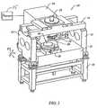
- FIG. 1is a perspective view of a lithographic system in accordance with the present invention
- FIG. 2is a simplified elevation view of a lithographic system shown in FIG. 1 ;
- FIG. 3is a simplified representation of material from which an imprinting layer, shown in FIG. 2 , is comprised before being polymerized and cross-linked;
- FIG. 4is a simplified representation of cross-linked polymer material into which the material shown in FIG. 3 is transformed after being subjected to radiation;
- FIG. 5is a simplified elevation view of a mold spaced-apart from the imprinting layer, shown in FIG. 1 , after patterning of the imprinting layer;
- FIG. 6is a simplified elevation view of an additional imprinting layer positioned atop of the substrate, shown in FIG. 5 , after the pattern in the first imprinting layer is transferred therein;
- FIG. 7is a plan view of an imaging system employed to sense alignment marks
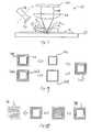
- FIG. 8is a plan view of alignment marks employed in accordance with the present invention.
- FIG. 9is a plan view of alignment marks employed in accordance with an alternate embodiment of the present invention.
- FIG. 10is a plan view of alignment marks employed in accordance with a second alternate embodiment of the present invention.
- FIG. 11is a plan view showing alignment marks disposed on a template, shown in FIG. 1 ;
- FIG. 12is a plan view of a template showing an arrangement of alignment marks thereon in accordance with an alternate embodiment of the present invention.
- FIG. 13is a cross-sectional view of the template shown in FIG. 12 taken along lines 13 - 13 ;
- FIG. 14is a plan view of a template showing an arrangement of alignment marks thereon in accordance with a third alternate embodiment of the present invention.
- FIG. 15is a plan view of a template showing an arrangement of alignment marks thereon in accordance with a fourth alternate embodiment of the present invention.
- FIG. 1depicts a lithographic system 10 in accordance with one embodiment of the present invention that includes a pair of spaced-apart bridge supports 12 having a bridge 14 and a stage support 16 extending therebetween. Bridge 14 and stage support 16 are spaced-apart. Coupled to bridge 14 is an imprint head 18 , which extends from bridge 14 toward stage support 16 and provides movement along the Z-axis. Disposed upon stage support 16 to face imprint head 18 is a motion stage 20 . Motion stage 20 is configured to move with respect to stage support 16 along X- and Y-axes.
- imprint head 18may provide movement along the X- and Y-axes, as well as the Z-axis
- motion stage 20may provide movement in the Z-axis, as well as the X- and Y-axes.
- An exemplary motion stage deviceis disclosed in U.S. patent application Ser. No. 10/194,414, filed Jul. 11, 2002, entitled “Step and Repeat Imprint Lithography Systems,” assigned to the assignee of the present invention, and which is incorporated by reference herein in its entirety.
- a radiation source 22is coupled to lithographic system 10 to impinge actinic radiation upon motion stage 20 .
- radiation source 22is coupled to bridge 14 and includes a power generator 23 connected to radiation source 22 .
- Operation of lithographic system 10is typically controlled by a processor 25 that is in data communication therewith.
- Mold 28includes a plurality of features defined by a plurality of spaced-apart recessions 28 a and protrusions 28 b .
- the plurality of featuresdefines an original pattern that is to be transferred into a substrate 30 positioned on motion stage 20 .
- imprint head 18 and/or motion stage 20may vary a distance “d” between mold 28 and substrate 30 .
- the features on mold 28may be imprinted into a flowable region of substrate 30 , discussed more fully below.
- Radiation source 22is located so that mold 28 is positioned between radiation source 22 and substrate 30 .
- mold 28is fabricated from a material that allows it to be substantially transparent to the radiation produced by radiation source 22 .
- a flowable regionsuch as an imprinting layer 34 , is disposed on a portion of a surface 32 that presents a substantially planar profile.
- a flowable regionmay be formed using any known technique, such as a hot embossing process disclosed in U.S. Pat. No. 5,772,905, which is incorporated by reference in its entirety herein, or a laser assisted direct imprinting (LADI) process of the type described by Chou et al. in Ultrafast and Direct Imprint of Nanostructures in Silicon, Nature , Col. 417, pp. 835-837, June 2002.
- LADIlaser assisted direct imprinting
- a flowable regionconsists of imprinting layer 34 being deposited as a plurality of spaced-apart discrete beads 36 of a material 36 a on substrate 30 , discussed more fully below.
- An exemplary system for depositing beads 36is disclosed in U.S. patent application Ser. No. 10/191,749, filed Jul. 9, 2002, entitled “System and Method for Dispensing Liquids,” and which is assigned to the assignee of the present invention, and which is incorporated by reference in its entirety herein.
- Imprinting layer 34is formed from material 36 a that may be selectively polymerized and cross-linked to record the original pattern therein, defining a recorded pattern.
- An exemplary composition for material 36 ais disclosed in U.S. patent application Ser. No.
- Material 36 ais shown in FIG. 4 as being cross-linked at points 36 b , forming a cross-linked polymer material 36 c.
- the pattern recorded in imprinting layer 34is produced, in part, by mechanical contact with mold 28 .
- distance “d”is reduced to allow imprinting beads 36 to come into mechanical contact with mold 28 , spreading beads 36 so as to form imprinting layer 34 with a contiguous formation of material 36 a over surface 32 .
- distance “d”is reduced to allow sub-portions 34 a of imprinting layer 34 to ingress into and fill recessions 28 a.
- material 36 ais provided with the requisite properties to completely fill recessions 28 a , while covering surface 32 with a contiguous formation of material 36 a .
- sub-portions 34 b of imprinting layer 34 in superimposition with protrusions 28 bremain after the desired, usually minimum, distance “d”, has been reached, leaving sub-portions 34 a with a thickness t 1 , and sub-portions 34 b with a thickness t 2 .
- Thicknesses “t 1 ” and “t 2 ”may be any thickness desired, dependent upon the application.
- t 1is selected so as to be no greater than twice the width u of sub-portions 34 a , i.e., t 1 ⁇ 2u, shown more clearly in FIG. 5 .
- radiation source 22produces actinic radiation that polymerizes and cross-links material 36 a , forming cross-linked polymer material 36 c .
- the composition of imprinting layer 34transforms from material 36 a to cross-linked polymer material 36 c , which is a solid.
- cross-linked polymer material 36 cis solidified to provide side 34 c of imprinting layer 34 with a shape conforming to a shape of a surface 28 c of mold 28 , shown more clearly in FIG. 5 .
- imprint head 18shown in FIG. 2 , is moved to increase distance “d” so that mold 28 and imprinting layer 34 are spaced-apart.
- substrate 30 and imprinting layer 34may be etched to transfer the pattern of imprinting layer 34 into substrate 30 , providing a patterned surface 32 a , shown in FIG. 6 .
- the material from which imprinting layer 34 is formedmay be varied to define a relative etch rate with respect to substrate 30 , as desired.
- the relative etch rate of imprinting layer 34 to substrate 30may be in a range of about 1.5:1 to about 100:1.
- imprinting layer 34may be provided with an etch differential with respect to photo-resist material (not shown) selectively disposed thereon.
- the photo-resist material (not shown)may be provided to further pattern imprinting layer 34 , using known techniques. Any etch process may be employed, dependent upon the etch rate desired and the underlying constituents that form substrate 30 and imprinting layer 34 . Exemplary etch processes may include plasma etching, reactive ion etching, chemical wet etching and the like.
- overlay alignment schemesmay include alignment error measurement and/or alignment error compensation and/or placement error measurement and correction.
- Placement errorgenerally refers to X-Y positioning errors between a template and a substrate (that is, translation along the X- and/or Y-axis). Placement errors, in one embodiment, are determined and corrected for by using an optical imaging system 40 , shown in FIG. 7 , to sense alignment marks discussed below with respect to FIG. 8 .
- optical imaging system 40includes a light source 42 and an optical train 44 to focus light upon substrate 30 .
- Optical imaging system 40is configured to focus alignment marks lying in differing focal planes onto a single focal plane, P, wherein an optical sensor 46 may be positioned.
- optical train 44is configured to provide wavelength-dependent focal lengths. Differing wavelengths of light may be produced in any manner known in the art.
- a single broadband source of lightshown as a light 48 , may produce wavelengths that impinge upon optical train 44 .
- Optical band-pass filtersmay be disposed between the broadband source and the alignment marks (not shown).
- Light 48is focused by optical train 44 to impinge upon alignment marks (not shown) at one or more regions, shown as region R 1 and region R 2 .
- Lightreflects from regions R 1 and R 2 , shown as a reflected light 50 , and is collected by a collector lens 52 .
- Collection lens 52focuses all wavelengths of reflected light 50 onto plane P so that optical sensor 46 detects reflected light 50 .
- alignment marksmay be of many configurations and are arranged in pairs with one of the alignment marks of the pair being disposed on template 26 and the remaining alignment mark being positioned on substrate 30 , typically in a previously deposited imprinting layer.
- alignment marksmay include first and second polygonal marks 60 and 62 , depicted as squares, but may be any polygonal shape desired.
- Another configuration for alignment marksare shown as crosses, shown as 64 and 66 .
- additional alignment marksmay be employed, such as vernier marks 68 and 70 , as well as Moiré gratings, shown as 72 and 74 .
- Wavelengthsare selected to obtain a desired focal length, depending upon the gap between mold 28 and substrate 30 .
- each overlay markmay produce two images on the imaging plane.
- a first polygonal alignment mark 60using a specific wavelength of light, presents as a focused image on sensor 46 .
- a second polygonal alignment mark 62using the same wavelength of light, presents as an out-of-focus image on sensor 46 . In order to eliminate each out-of-focus image, several methods may be used.
- two imagesmay be received by an imaging device, such as sensor 46 , sensing first and second polygonal marks 162 and 164 .
- an imaging devicesuch as sensor 46 , sensing first and second polygonal marks 162 and 164 .
- polygonal mark 162is focused and polygonal mark 164 is out-of-focus.
- An image processing techniquemay be used to remove geometric data corresponding to pixels associated with polygonal mark 164 .
- the out-of-focus polygonal mark of the substrate markmay be eliminated, leaving only polygonal mark 162 .
- polygonal marks 262 and 264may be sensed by sensor 46 .
- polygonal marks 262 and 264are not focused by collection lens 52 on sensor 46 , shown a polygonal mark 262 , but polygonal mark 264 is focused onto sensor 46 . As before, geometric data associated with polygonal mark 262 is removed, leaving only geometric data associated with polygonal mark 264 . Thereafter, polygonal marks 162 and 264 are superimposed forming alignment marks 265 to ascertain alignment between template and substrate.
- a second methodmay utilize two coplanar polarizing arrays, shown in FIG. 10 , and polarized illumination sources.
- Alignment marksmay include orthogonally polarizing arrays 76 .
- Polarizing arrays 78are formed on a surface of mold 28 or placed above the surface. Under two polarized illumination sources, only focused images 78 (each corresponding to a distinct wavelength and polarization) may appear on an imaging plane. Thus, out-of-focus images are filtered out by polarizing arrays 76 .
- An advantage of this methodmay be that it may not require an image processing technique to eliminate out-of-focus images.
- Moiré pattern based overlay measurementhas been used for optical lithography processes.
- For imprint lithography processeswhere two layers of Moiré patterns are not on the same plane but still overlap in the imaging array, acquiring two individual focused images may be difficult to achieve.
- carefully controlling the gap between template 26 and substrate 30 within the depth of focus of the optical measurement tool and without direct contact between template 26 and substrate 30may allow two layers of Moiré patterns to be simultaneously acquired with minimal focusing problems. It is believed that other standard overlay schemes based on the Moiré patterns may be directly implemented to imprint lithography process.
- overlay marks 80Another concern with overlay alignment for imprint lithography processes that employ UV curable liquid materials may be the visibility of the alignment marks.
- two overlay markssuch as the marks discussed above with respect to FIGS. 8, 9 and 10 , are employed, referred to collectively as overlay marks 80 .
- the template overlay marksare not opaque lines. Rather, the template overlay marks are topographical features of the template surface.
- the overlay marksare made of the same material as the template.
- UV curable liquidsmay have a refractive index that is similar to the refractive index of the template materials, e.g., quartz.
- template overlay marksmay become very difficult to recognize. If the template overlay marks are made with an opaque material, e.g., chromium or nickel, the UV curable liquid below the overlay marks may not be properly exposed to the UV light.
- an opaque materiale.g., chromium or nickel
- overlay marksare used on template 26 that are seen by optical imaging system 40 but are opaque to the curing light, e.g., uv light.
- An embodiment of this approachis illustrated in FIG. 11 .
- overlay marks 80 on the templatemay be formed of fine polarizing lines 82 .
- suitable fine polarizing lines 82have a width about 1 ⁇ 2 to 1 ⁇ 4 of the wavelength of activating light used as the curing agent.
- the line width of fine polarizing lines 82should be small enough so that activating light passing between two lines is diffracted sufficiently to cause curing of all the liquid below the lines.
- the activating lightmay be polarized according to the polarization of overlay marks 80 .
- Polarizing the activating lightprovides a relatively uniform exposure to all regions of template 26 , including regions having overlay marks 80 .
- Light used to locate overlay marks 80 on template 26may be broadband light or a specific wavelength that may not cure the liquid material. This light need not be polarized.
- Fine polarizing lines 82are substantially opaque to the measuring light, thus making overlay marks 80 visible using established overlay error measuring tools. Fine polarized overlay marks are fabricated on template 26 using existing techniques, such as electron beam lithography.
- overlay marks 80are formed of a different material than template 26 .
- a material selected to form the template overlay marksmay be substantially opaque to visible light but transparent to activating light used as the curing agent, e.g., UV light.
- SiO xwhere x is less than 2
- structures formed of SiO xwhere x is about 1.5, are substantially opaque to visible light, but transparent to UV curing light.
- alignment marksmay be formed from a metal, i.e., chromium, nickel, and the like. In this manner, alignment marks 80 are opaque to both the analyzing light and the activating light.
- alignment marks 80may be positioned outside of the imprinting area, e.g., alignment marks 80 may be positioned in a region in which no features are patterned.
- a template 326includes four molds 328 , 330 , 332 and 334 , each of which has features f 1 , f 2 , f 3 and f 4 , respectively, with alignment marks 80 disposed in a region of template 326 outside of molds 328 , 330 , 332 and 334 .
- alignment marks 80are surrounded by a moat system 336 . This is important as the opaqueness of alignment marks 1302 formed from metal would hinder, if not prevent, solidification of curable liquid. Segments 336 a , 336 b , 336 c and 336 d of moat system 336 separate molds 328 , 330 , 332 and 334 .
- segments 336 a , 336 b , 336 c and 336 dhave a sufficient depth to curable liquid from substantially egressing therein from adjacent active molds 328 , 330 , 332 and 334 due to capillary forces.
- moat system 336may include a segment 336 e that surrounds molds 328 , 330 , 332 and 334 .
- alignment marks 80may be placed within a mold, shown as a mold 428 .
- the region of mold 428 in which alignment marks 80 are positioneddoes not include any patterned features.
- Alignment marks 80are surrounded by moat 436 so as to prevent liquid imprinting material from coming into contact therewith for the reasons discussed above with respect to FIGS. 11 and 12 .
- an additional set of alignment marksmay be included in a region outside of molds 428 , 330 , 332 , 334 , shown as alignment marks 180 .
- alignment marks 280 and 282may be disposed at opposite corners of a mold, such as a template 528 shown in FIG. 15 .
- Alignment marks 280 and 282may or may not be surrounded by a moat to prevent liquid imprinting material from coming into contact therewith, as discussed above with respect to moat 436 in FIG. 14 . Additionally, it has been found desirable to have at least one of alignment marks 280 and 282 not surrounded by a moat and not formed from opaque material.
- alignment marks 80 formed from metalmay be employed without degrading the underlying pattern generated during imprinting.
- Employing metal alignment marksmay reduce the processing time required when manufacturing template 326 .
- template 326may be patterned with features f 1 , f 2 , f 3 , and f 4 , as well as alignment marks 80 using e-beam lithography.
- chromium or some other metalsis employed as masking material during e-beam patterning processes. Arranging alignment marks 80 as discussed above would enable leaving masking metals in the region of alignment marks 80 after e-beam patterning.
Landscapes
- Engineering & Computer Science (AREA)
- Physics & Mathematics (AREA)
- Chemical & Material Sciences (AREA)
- Nanotechnology (AREA)
- General Physics & Mathematics (AREA)
- Crystallography & Structural Chemistry (AREA)
- Mathematical Physics (AREA)
- Theoretical Computer Science (AREA)
- Condensed Matter Physics & Semiconductors (AREA)
- Manufacturing & Machinery (AREA)
- Exposure Of Semiconductors, Excluding Electron Or Ion Beam Exposure (AREA)
- Shaping Of Tube Ends By Bending Or Straightening (AREA)
Abstract
Description
- The field of invention relates generally to imprint lithography. More particularly, the present invention is directed to producing templates having alignment marks formed thereon.
- Micro-fabrication involves the fabrication of very small structures, e.g., having features on the order of micro-meters or smaller. One area in which micro-fabrication has had a sizeable impact is in the processing of integrated circuits. As the semiconductor processing industry continues to strive for larger production yields while increasing the circuits per unit area formed on a substrate, micro-fabrication becomes increasingly important. Micro-fabrication provides greater process control while allowing increased reduction of the minimum feature dimension of the structures formed. Other areas of development in which micro-fabrication has been employed include biotechnology, optical technology, mechanical systems and the like.
- An exemplary micro-fabrication technique is shown in U.S. Pat. No. 6,334,960 to Willson et al. Willson et al. disclose a method of forming a relief image in a structure. The method includes providing a substrate having a transfer layer. The transfer layer is covered with a polymerizable fluid composition. A mold makes mechanical contact with the polymerizable fluid. The mold includes a relief structure, and the polymerizable fluid composition fills the relief structure. The polymerizable fluid composition is then subjected to conditions to solidify and polymerize the same, forming a solidified polymeric material on the transfer layer that contains a relief structure complimentary to that of the mold. The mold is then separated from the solid polymeric material such that a replica of the relief structure in the mold is formed in the solidified polymeric material. The transfer layer and the solidified polymeric material are subjected to an environment to selectively etch the transfer layer relative to the solidified polymeric material such that a relief image is formed in the transfer layer. The time required and the minimum feature dimension provided by this technique are dependent upon, inter alia, the composition of the polymerizable material.
- U.S. Pat. No. 5,772,905 to Chou discloses a lithographic method and an apparatus for creating ultra-fine (sub-25 nm) patterns in a thin film coated on a substrate in which a mold having at least one protruding feature is pressed into a thin film carried on a substrate. The protruding feature in the mold creates a recess of the thin film. The mold is removed from the film. The thin film then is processed such that the thin film in the recess is removed exposing the underlying substrate. Thus, patterns in the mold are replaced in the thin film, completing the lithography. The patterns in the thin film will be, in subsequent processes, reproduced in the substrate or in another material which is added onto the substrate.
- Yet another imprint lithography technique is disclosed by Chou et al. inUltrafast and Direct Imprint of Nanostructures in Silicon, Nature, Col. 417, pp. 835-837, June 2002, which is referred to as a laser assisted direct imprinting (LADI) process. In this process, a region of a substrate is made flowable, e.g., liquefied, by heating the region with the laser. After the region has reached a desired viscosity, a mold, having a pattern thereon, is placed in contact with the region. The flowable region conforms to the profile of the pattern and is then cooled, solidifying the pattern into the substrate. A concern with each of the above-identified pattern formation processes relates to proper orientation of the template with the substrate. For example, it is desired to properly align the template with an existing patterned layer so that the proper orientation between the existing patterned layer and a subsequent patterned layer is obtained.
- Thus, a need exists for producing a template having alignment marks for use with imprint lithographic techniques.
- The present invention is directed to providing a template with alignment marks that are opaque to selective wavelength of light. In one embodiment, a template is provided having patterning areas and a template, with the template mark being formed from metal and disposed outside of the patterning areas. The alignment marks may be surrounded by a moat to prevent curable liquid from being in superimposition therewith during imprinting. In this manner, opaque alignment marks may be employed without degrading the quality of the pattern formed during imprinting. These and other embodiments are discussed more fully below.
FIG. 1 is a perspective view of a lithographic system in accordance with the present invention;FIG. 2 is a simplified elevation view of a lithographic system shown inFIG. 1 ;FIG. 3 is a simplified representation of material from which an imprinting layer, shown inFIG. 2 , is comprised before being polymerized and cross-linked;FIG. 4 is a simplified representation of cross-linked polymer material into which the material shown inFIG. 3 is transformed after being subjected to radiation;FIG. 5 is a simplified elevation view of a mold spaced-apart from the imprinting layer, shown inFIG. 1 , after patterning of the imprinting layer;FIG. 6 is a simplified elevation view of an additional imprinting layer positioned atop of the substrate, shown inFIG. 5 , after the pattern in the first imprinting layer is transferred therein;FIG. 7 is a plan view of an imaging system employed to sense alignment marks;FIG. 8 is a plan view of alignment marks employed in accordance with the present invention;FIG. 9 is a plan view of alignment marks employed in accordance with an alternate embodiment of the present invention;FIG. 10 is a plan view of alignment marks employed in accordance with a second alternate embodiment of the present invention;FIG. 11 is a plan view showing alignment marks disposed on a template, shown inFIG. 1 ;FIG. 12 is a plan view of a template showing an arrangement of alignment marks thereon in accordance with an alternate embodiment of the present invention;FIG. 13 is a cross-sectional view of the template shown inFIG. 12 taken along lines13-13;FIG. 14 is a plan view of a template showing an arrangement of alignment marks thereon in accordance with a third alternate embodiment of the present invention; andFIG. 15 is a plan view of a template showing an arrangement of alignment marks thereon in accordance with a fourth alternate embodiment of the present invention;FIG. 1 depicts alithographic system 10 in accordance with one embodiment of the present invention that includes a pair of spaced-apart bridge supports12 having abridge 14 and astage support 16 extending therebetween.Bridge 14 andstage support 16 are spaced-apart. Coupled tobridge 14 is animprint head 18, which extends frombridge 14 towardstage support 16 and provides movement along the Z-axis. Disposed uponstage support 16 to faceimprint head 18 is amotion stage 20.Motion stage 20 is configured to move with respect tostage support 16 along X- and Y-axes. It should be understood thatimprint head 18 may provide movement along the X- and Y-axes, as well as the Z-axis, andmotion stage 20 may provide movement in the Z-axis, as well as the X- and Y-axes. An exemplary motion stage device is disclosed in U.S. patent application Ser. No. 10/194,414, filed Jul. 11, 2002, entitled “Step and Repeat Imprint Lithography Systems,” assigned to the assignee of the present invention, and which is incorporated by reference herein in its entirety. Aradiation source 22 is coupled tolithographic system 10 to impinge actinic radiation uponmotion stage 20. As shown,radiation source 22 is coupled tobridge 14 and includes apower generator 23 connected toradiation source 22. Operation oflithographic system 10 is typically controlled by aprocessor 25 that is in data communication therewith.- Referring to both
FIGS. 1 and 2 , connected toimprint head 18 is atemplate 26 having amold 28 thereon.Mold 28 includes a plurality of features defined by a plurality of spaced-apart recessions 28aandprotrusions 28b. The plurality of features defines an original pattern that is to be transferred into asubstrate 30 positioned onmotion stage 20. To that end,imprint head 18 and/ormotion stage 20 may vary a distance “d” betweenmold 28 andsubstrate 30. In this manner, the features onmold 28 may be imprinted into a flowable region ofsubstrate 30, discussed more fully below.Radiation source 22 is located so thatmold 28 is positioned betweenradiation source 22 andsubstrate 30. As a result,mold 28 is fabricated from a material that allows it to be substantially transparent to the radiation produced byradiation source 22. - Referring to both
FIGS. 2 and 3 , a flowable region, such as animprinting layer 34, is disposed on a portion of asurface 32 that presents a substantially planar profile. A flowable region may be formed using any known technique, such as a hot embossing process disclosed in U.S. Pat. No. 5,772,905, which is incorporated by reference in its entirety herein, or a laser assisted direct imprinting (LADI) process of the type described by Chou et al. inUltrafast and Direct Imprint of Nanostructures in Silicon, Nature, Col. 417, pp. 835-837, June 2002. In the present embodiment, however, a flowable region consists ofimprinting layer 34 being deposited as a plurality of spaced-apartdiscrete beads 36 of a material36aonsubstrate 30, discussed more fully below. An exemplary system for depositingbeads 36 is disclosed in U.S. patent application Ser. No. 10/191,749, filed Jul. 9, 2002, entitled “System and Method for Dispensing Liquids,” and which is assigned to the assignee of the present invention, and which is incorporated by reference in its entirety herein. Imprintinglayer 34 is formed frommaterial 36athat may be selectively polymerized and cross-linked to record the original pattern therein, defining a recorded pattern. An exemplary composition formaterial 36ais disclosed in U.S. patent application Ser. No. 10/463,396, filed Jun. 16, 2003 and entitled “Method to Reduce Adhesion Between a Conformable Region and a Pattern of a Mold,” which is incorporated by reference in its entirety herein.Material 36ais shown inFIG. 4 as being cross-linked atpoints 36b, forming across-linked polymer material 36c. - Referring to
FIGS. 2, 3 and5, the pattern recorded inimprinting layer 34 is produced, in part, by mechanical contact withmold 28. To that end, distance “d” is reduced to allowimprinting beads 36 to come into mechanical contact withmold 28, spreadingbeads 36 so as to form imprintinglayer 34 with a contiguous formation ofmaterial 36aoversurface 32. In one embodiment, distance “d” is reduced to allow sub-portions34aofimprinting layer 34 to ingress into and fillrecessions 28a. - To facilitate filling of
recessions 28a,material 36ais provided with the requisite properties to completely fillrecessions 28a, while coveringsurface 32 with a contiguous formation ofmaterial 36a. In the present embodiment, sub-portions34bofimprinting layer 34 in superimposition withprotrusions 28bremain after the desired, usually minimum, distance “d”, has been reached, leaving sub-portions34awith a thickness t1, and sub-portions34bwith a thickness t2. Thicknesses “t1” and “t2” may be any thickness desired, dependent upon the application. Typically, t1is selected so as to be no greater than twice the width u of sub-portions34a, i.e., t1≦2u, shown more clearly inFIG. 5 . - Referring to
FIGS. 2, 3 and4, after a desired distance “d” has been reached,radiation source 22 produces actinic radiation that polymerizes andcross-links material 36a, formingcross-linked polymer material 36c. As a result, the composition ofimprinting layer 34 transforms frommaterial 36atocross-linked polymer material 36c, which is a solid. Specifically,cross-linked polymer material 36cis solidified to provide side34cofimprinting layer 34 with a shape conforming to a shape of asurface 28cofmold 28, shown more clearly inFIG. 5 . After imprintinglayer 34 is transformed to consist ofcross-linked polymer material 36c, shown inFIG. 4 ,imprint head 18, shown inFIG. 2 , is moved to increase distance “d” so thatmold 28 andimprinting layer 34 are spaced-apart. - Referring to
FIG. 5 , additional processing may be employed to complete the patterning ofsubstrate 30. For example,substrate 30 andimprinting layer 34 may be etched to transfer the pattern ofimprinting layer 34 intosubstrate 30, providing a patternedsurface 32a, shown inFIG. 6 . To facilitate etching, the material from whichimprinting layer 34 is formed may be varied to define a relative etch rate with respect tosubstrate 30, as desired. The relative etch rate ofimprinting layer 34 tosubstrate 30 may be in a range of about 1.5:1 to about 100:1. - Alternatively, or in addition to,
imprinting layer 34 may be provided with an etch differential with respect to photo-resist material (not shown) selectively disposed thereon. The photo-resist material (not shown) may be provided to furtherpattern imprinting layer 34, using known techniques. Any etch process may be employed, dependent upon the etch rate desired and the underlying constituents that formsubstrate 30 andimprinting layer 34. Exemplary etch processes may include plasma etching, reactive ion etching, chemical wet etching and the like. - To form an additional imprinting layer, such as a
layer 124 atop ofsurface 32a, correct placement ofmold 28 with respect tosubstrate 30 is important. To that end, overlay alignment schemes may include alignment error measurement and/or alignment error compensation and/or placement error measurement and correction. Placement error, as used herein, generally refers to X-Y positioning errors between a template and a substrate (that is, translation along the X- and/or Y-axis). Placement errors, in one embodiment, are determined and corrected for by using an optical imaging system40, shown inFIG. 7 , to sense alignment marks discussed below with respect toFIG. 8 . - Referring to
FIG. 7 , optical imaging system40 includes alight source 42 and anoptical train 44 to focus light uponsubstrate 30. Optical imaging system40 is configured to focus alignment marks lying in differing focal planes onto a single focal plane, P, wherein anoptical sensor 46 may be positioned. As a result,optical train 44 is configured to provide wavelength-dependent focal lengths. Differing wavelengths of light may be produced in any manner known in the art. For example, a single broadband source of light, shown as a light48, may produce wavelengths that impinge uponoptical train 44. Optical band-pass filters (not shown) may be disposed between the broadband source and the alignment marks (not shown). Alternatively, a plurality of sources of light (not shown) may be employed, each one of which produces distinct wavelengths of light.Light 48 is focused byoptical train 44 to impinge upon alignment marks (not shown) at one or more regions, shown as region R1and region R2. Light reflects from regions R1and R2, shown as a reflected light50, and is collected by a collector lens52. Collection lens52 focuses all wavelengths of reflected light50 onto plane P so thatoptical sensor 46 detects reflected light50. - Referring to
FIGS. 1 and 8 , alignment marks may be of many configurations and are arranged in pairs with one of the alignment marks of the pair being disposed ontemplate 26 and the remaining alignment mark being positioned onsubstrate 30, typically in a previously deposited imprinting layer. For example, alignment marks may include first and second polygonal marks60 and62, depicted as squares, but may be any polygonal shape desired. Another configuration for alignment marks are shown as crosses, shown as64 and66. Also additional alignment marks may be employed, such as vernier marks68 and70, as well as Moiré gratings, shown as72 and74. - Wavelengths are selected to obtain a desired focal length, depending upon the gap between
mold 28 andsubstrate 30. Under each wavelength of light used, each overlay mark may produce two images on the imaging plane. A first polygonal alignment mark60, using a specific wavelength of light, presents as a focused image onsensor 46. A second polygonal alignment mark62, using the same wavelength of light, presents as an out-of-focus image onsensor 46. In order to eliminate each out-of-focus image, several methods may be used. - Referring to
FIGS. 7 and 8 , in a first method, under illumination with a first wavelength of light, two images may be received by an imaging device, such assensor 46, sensing first and secondpolygonal marks polygonal mark 162 is focused andpolygonal mark 164 is out-of-focus. An image processing technique may be used to remove geometric data corresponding to pixels associated withpolygonal mark 164. Thus, the out-of-focus polygonal mark of the substrate mark may be eliminated, leaving onlypolygonal mark 162. Using the same procedure and a second wavelength of light,polygonal marks sensor 46. One of thepolygonal marks sensor 46, shown apolygonal mark 262, butpolygonal mark 264 is focused ontosensor 46. As before, geometric data associated withpolygonal mark 262 is removed, leaving only geometric data associated withpolygonal mark 264. Thereafter,polygonal marks - A second method may utilize two coplanar polarizing arrays, shown in
FIG. 10 , and polarized illumination sources. Alignment marks may include orthogonallypolarizing arrays 76. Polarizing arrays78 are formed on a surface ofmold 28 or placed above the surface. Under two polarized illumination sources, only focused images78 (each corresponding to a distinct wavelength and polarization) may appear on an imaging plane. Thus, out-of-focus images are filtered out by polarizingarrays 76. An advantage of this method may be that it may not require an image processing technique to eliminate out-of-focus images. - Referring to
FIGS. 1 and 11 , Moiré pattern based overlay measurement has been used for optical lithography processes. For imprint lithography processes, where two layers of Moiré patterns are not on the same plane but still overlap in the imaging array, acquiring two individual focused images may be difficult to achieve. However, carefully controlling the gap betweentemplate 26 andsubstrate 30 within the depth of focus of the optical measurement tool and without direct contact betweentemplate 26 andsubstrate 30 may allow two layers of Moiré patterns to be simultaneously acquired with minimal focusing problems. It is believed that other standard overlay schemes based on the Moiré patterns may be directly implemented to imprint lithography process. - Another concern with overlay alignment for imprint lithography processes that employ UV curable liquid materials may be the visibility of the alignment marks. For the overlay placement error measurement, two overlay marks, such as the marks discussed above with respect to
FIGS. 8, 9 and10, are employed, referred to collectively as overlay marks80. However, since it is desirable fortemplate 26 to be transparent to a curing agent, the template overlay marks, in some embodiments, are not opaque lines. Rather, the template overlay marks are topographical features of the template surface. In some embodiments, the overlay marks are made of the same material as the template. In addition, UV curable liquids may have a refractive index that is similar to the refractive index of the template materials, e.g., quartz. Therefore, when the UV curable liquid fills the gap betweentemplate 26 andsubstrate 30, template overlay marks may become very difficult to recognize. If the template overlay marks are made with an opaque material, e.g., chromium or nickel, the UV curable liquid below the overlay marks may not be properly exposed to the UV light. - In an embodiment, overlay marks are used on
template 26 that are seen by optical imaging system40 but are opaque to the curing light, e.g., uv light. An embodiment of this approach is illustrated inFIG. 11 . Instead of completely opaque lines, overlay marks80 on the template may be formed of finepolarizing lines 82. For example, suitable finepolarizing lines 82 have a width about ½ to ¼ of the wavelength of activating light used as the curing agent. The line width of finepolarizing lines 82 should be small enough so that activating light passing between two lines is diffracted sufficiently to cause curing of all the liquid below the lines. In such an embodiment, the activating light may be polarized according to the polarization of overlay marks80. Polarizing the activating light provides a relatively uniform exposure to all regions oftemplate 26, including regions having overlay marks80. Light used to locate overlay marks80 ontemplate 26 may be broadband light or a specific wavelength that may not cure the liquid material. This light need not be polarized. Finepolarizing lines 82 are substantially opaque to the measuring light, thus making overlay marks80 visible using established overlay error measuring tools. Fine polarized overlay marks are fabricated ontemplate 26 using existing techniques, such as electron beam lithography. - In another embodiment, overlay marks80 are formed of a different material than
template 26. For example, a material selected to form the template overlay marks may be substantially opaque to visible light but transparent to activating light used as the curing agent, e.g., UV light. For example, SiOx, where x is less than 2, may be used as such a material. In particular, structures formed of SiOx, where x is about 1.5, are substantially opaque to visible light, but transparent to UV curing light. Alternatively, or in conjunction with the SiOx, alignment marks may be formed from a metal, i.e., chromium, nickel, and the like. In this manner, alignment marks80 are opaque to both the analyzing light and the activating light. To ensure that alignment marks80, such as the metal alignment marks, do not compromise the imprint pattern by, inter alia, blocking the activating light, alignment marks80 may be positioned outside of the imprinting area, e.g., alignment marks80 may be positioned in a region in which no features are patterned. To that end, atemplate 326 includes fourmolds template 326 outside ofmolds - Referring to
FIGS. 12 and 13 , to prevent imprinting material (not shown) from entering a region ofsubstrate 30 in superimposition with alignment marks80, alignment marks80 are surrounded by amoat system 336. This is important as the opaqueness of alignment marks1302 formed from metal would hinder, if not prevent, solidification of curable liquid.Segments moat system 336separate molds segments active molds moat system 336 may include asegment 336ethat surroundsmolds - Referring to
FIG. 14 in another embodiment, alignment marks80 may be placed within a mold, shown as a mold428. However, the region of mold428 in which alignment marks80 are positioned does not include any patterned features. Alignment marks80 are surrounded bymoat 436 so as to prevent liquid imprinting material from coming into contact therewith for the reasons discussed above with respect toFIGS. 11 and 12 . Alternatively, an additional set of alignment marks may be included in a region outside ofmolds template 528 shown inFIG. 15 . Alignment marks280 and282 may or may not be surrounded by a moat to prevent liquid imprinting material from coming into contact therewith, as discussed above with respect tomoat 436 inFIG. 14 . Additionally, it has been found desirable to have at least one of alignment marks280 and282 not surrounded by a moat and not formed from opaque material. - From the foregoing, it is seen that alignment marks80 formed from metal may be employed without degrading the underlying pattern generated during imprinting. Employing metal alignment marks may reduce the processing time required when manufacturing
template 326. For example,template 326 may be patterned with features f1, f2, f3, and f4, as well as alignment marks80 using e-beam lithography. As is well known, chromium or some other metals is employed as masking material during e-beam patterning processes. Arranging alignment marks80 as discussed above would enable leaving masking metals in the region of alignment marks80 after e-beam patterning. - The embodiments of the present invention described above are exemplary. Many changes and modifications may be made to the disclosure recited above, while remaining within the scope of the invention. Therefore, the scope of the invention should not be limited by the above description, but instead should be determined with reference to the appended claims along with their full scope of equivalents.
Claims (20)
Priority Applications (1)
| Application Number | Priority Date | Filing Date | Title |
|---|---|---|---|
| US10/670,980US7136150B2 (en) | 2003-09-25 | 2003-09-25 | Imprint lithography template having opaque alignment marks |
Applications Claiming Priority (1)
| Application Number | Priority Date | Filing Date | Title |
|---|---|---|---|
| US10/670,980US7136150B2 (en) | 2003-09-25 | 2003-09-25 | Imprint lithography template having opaque alignment marks |
Publications (2)
| Publication Number | Publication Date |
|---|---|
| US20050067379A1true US20050067379A1 (en) | 2005-03-31 |
| US7136150B2 US7136150B2 (en) | 2006-11-14 |
Family
ID=34376049
Family Applications (1)
| Application Number | Title | Priority Date | Filing Date |
|---|---|---|---|
| US10/670,980Expired - LifetimeUS7136150B2 (en) | 2003-09-25 | 2003-09-25 | Imprint lithography template having opaque alignment marks |
Country Status (1)
| Country | Link |
|---|---|
| US (1) | US7136150B2 (en) |
Cited By (33)
| Publication number | Priority date | Publication date | Assignee | Title |
|---|---|---|---|---|
| US20030205657A1 (en)* | 2002-05-01 | 2003-11-06 | Voisin Ronald D. | Methods of manufacturing a lithography template |
| US20040163563A1 (en)* | 2000-07-16 | 2004-08-26 | The Board Of Regents, The University Of Texas System | Imprint lithography template having a mold to compensate for material changes of an underlying liquid |
| US20050051698A1 (en)* | 2002-07-08 | 2005-03-10 | Molecular Imprints, Inc. | Conforming template for patterning liquids disposed on substrates |
| US20050202350A1 (en)* | 2004-03-13 | 2005-09-15 | Colburn Matthew E. | Method for fabricating dual damascene structures using photo-imprint lithography, methods for fabricating imprint lithography molds for dual damascene structures, materials for imprintable dielectrics and equipment for photo-imprint lithography used in dual damascene patterning |
| US20050230882A1 (en)* | 2004-04-19 | 2005-10-20 | Molecular Imprints, Inc. | Method of forming a deep-featured template employed in imprint lithography |
| US20050236360A1 (en)* | 2004-04-27 | 2005-10-27 | Molecular Imprints, Inc. | Compliant hard template for UV imprinting |
| US20060032437A1 (en)* | 2004-08-13 | 2006-02-16 | Molecular Imprints, Inc. | Moat system for an imprint lithography template |
| US20060145398A1 (en)* | 2004-12-30 | 2006-07-06 | Board Of Regents, The University Of Texas System | Release layer comprising diamond-like carbon (DLC) or doped DLC with tunable composition for imprint lithography templates and contact masks |
| US20060177535A1 (en)* | 2005-02-04 | 2006-08-10 | Molecular Imprints, Inc. | Imprint lithography template to facilitate control of liquid movement |
| US20060267231A1 (en)* | 2005-05-27 | 2006-11-30 | Asml Netherlands B.V. | Imprint lithography |
| US20060266916A1 (en)* | 2005-05-25 | 2006-11-30 | Molecular Imprints, Inc. | Imprint lithography template having a coating to reflect and/or absorb actinic energy |
| US20060268256A1 (en)* | 2005-05-27 | 2006-11-30 | Asml Netherlands B.V. | Imprint lithography |
| US20070018360A1 (en)* | 2005-07-21 | 2007-01-25 | Asml Netherlands B.V. | Imprint lithography |
| EP1760526A1 (en)* | 2005-09-06 | 2007-03-07 | Canon Kabushiki Kaisha | Mold, imprint method, and process for producing chip |
| US20070176320A1 (en)* | 2006-02-01 | 2007-08-02 | Canon Kabushiki Kaisha | Mold for imprint, process for producing minute structure using the mold, and process for producing the mold |
| WO2007123249A2 (en) | 2006-04-18 | 2007-11-01 | Canon Kabushiki Kaisha | Alignment method, imprint method, alignment apparatus, and position measurement method |
| US20080090170A1 (en)* | 2006-10-04 | 2008-04-17 | Ikuo Yoneda | Pattern forming template and pattern forming method |
| US20090148619A1 (en)* | 2007-12-05 | 2009-06-11 | Molecular Imprints, Inc. | Controlling Thickness of Residual Layer |
| US7630067B2 (en) | 2004-11-30 | 2009-12-08 | Molecular Imprints, Inc. | Interferometric analysis method for the manufacture of nano-scale devices |
| US20100195102A1 (en)* | 2009-02-04 | 2010-08-05 | Asml Netherlands B.V. | Imprint lithography |
| US7785526B2 (en) | 2004-07-20 | 2010-08-31 | Molecular Imprints, Inc. | Imprint alignment method, system, and template |
| US20100233432A1 (en)* | 2007-08-03 | 2010-09-16 | Canon Kabushiki Kaisha | Imprint method and processing method of substrate |
| US20100278954A1 (en)* | 2006-04-03 | 2010-11-04 | Molecular Imprints, Inc. | Method of Concurrently Patterning a Substrate Having a Plurality of Fields and a Plurality of Alignment Marks |
| US20100285167A1 (en)* | 2005-06-17 | 2010-11-11 | Micron Technology, Inc. | Templates for use in imprint lithography and related intermediate template structures |
| WO2011072897A1 (en)* | 2009-12-18 | 2011-06-23 | Asml Netherlands B.V. | Imprint lithography |
| US20110192302A1 (en)* | 2010-02-05 | 2011-08-11 | Molecular Imprints, Inc. | Templates Having High Contrast Alignment Marks |
| US20110284499A1 (en)* | 2005-09-06 | 2011-11-24 | Canon Kabushiki Kaisha | Imprint method using a mold and process for producing structure using an imprint apparatus |
| CN104635422A (en)* | 2014-09-10 | 2015-05-20 | 苏州大学 | Nanoimprinting method and device of array micro structure |
| US20150165655A1 (en)* | 2011-04-25 | 2015-06-18 | Canon Nanotechnologies, Inc. | Optically Absorptive Material for Alignment Marks |
| JP2016066667A (en)* | 2014-09-24 | 2016-04-28 | 大日本印刷株式会社 | Template for imprinting and imprinting method |
| US10248018B2 (en)* | 2015-03-30 | 2019-04-02 | Canon Kabushiki Kaisha | Imprint apparatus and method of manufacturing article |
| US11249394B2 (en)* | 2011-10-14 | 2022-02-15 | Canon Kabushiki Kaisha | Imprint methods for forming a pattern of an imprint material on a substrate-side pattern region of a substrate by using a mold, and related device manufacturing methods |
| US20220301908A1 (en)* | 2021-03-16 | 2022-09-22 | Kioxia Corporation | Template, manufacturing method of template, and manufacturing method of semiconductor device |
Families Citing this family (29)
| Publication number | Priority date | Publication date | Assignee | Title |
|---|---|---|---|---|
| CN1262883C (en) | 2000-07-17 | 2006-07-05 | 得克萨斯州大学系统董事会 | Method and system of automatic fluid dispensing for imprint lithography processes |
| US20080160129A1 (en)* | 2006-05-11 | 2008-07-03 | Molecular Imprints, Inc. | Template Having a Varying Thickness to Facilitate Expelling a Gas Positioned Between a Substrate and the Template |
| GB0227902D0 (en)* | 2002-11-29 | 2003-01-08 | Ingenia Holdings Ltd | Template |
| US20070231421A1 (en)* | 2006-04-03 | 2007-10-04 | Molecular Imprints, Inc. | Enhanced Multi Channel Alignment |
| US8142850B2 (en) | 2006-04-03 | 2012-03-27 | Molecular Imprints, Inc. | Patterning a plurality of fields on a substrate to compensate for differing evaporation times |
| US8850980B2 (en)* | 2006-04-03 | 2014-10-07 | Canon Nanotechnologies, Inc. | Tessellated patterns in imprint lithography |
| US8012395B2 (en) | 2006-04-18 | 2011-09-06 | Molecular Imprints, Inc. | Template having alignment marks formed of contrast material |
| JP2010503993A (en) | 2006-09-19 | 2010-02-04 | モレキュラー・インプリンツ・インコーポレーテッド | Improved etching techniques for lift-off patterning |
| US7837907B2 (en)* | 2007-07-20 | 2010-11-23 | Molecular Imprints, Inc. | Alignment system and method for a substrate in a nano-imprint process |
| US7906274B2 (en)* | 2007-11-21 | 2011-03-15 | Molecular Imprints, Inc. | Method of creating a template employing a lift-off process |
| US20090147237A1 (en)* | 2007-12-05 | 2009-06-11 | Molecular Imprints, Inc. | Spatial Phase Feature Location |
| US8012394B2 (en)* | 2007-12-28 | 2011-09-06 | Molecular Imprints, Inc. | Template pattern density doubling |
| US8361371B2 (en)* | 2008-02-08 | 2013-01-29 | Molecular Imprints, Inc. | Extrusion reduction in imprint lithography |
| US20090212012A1 (en)* | 2008-02-27 | 2009-08-27 | Molecular Imprints, Inc. | Critical dimension control during template formation |
| US20100015270A1 (en)* | 2008-07-15 | 2010-01-21 | Molecular Imprints, Inc. | Inner cavity system for nano-imprint lithography |
| TW201022017A (en)* | 2008-09-30 | 2010-06-16 | Molecular Imprints Inc | Particle mitigation for imprint lithography |
| US20100092599A1 (en)* | 2008-10-10 | 2010-04-15 | Molecular Imprints, Inc. | Complementary Alignment Marks for Imprint Lithography |
| US20100095862A1 (en)* | 2008-10-22 | 2010-04-22 | Molecular Imprints, Inc. | Double Sidewall Angle Nano-Imprint Template |
| US8877073B2 (en)* | 2008-10-27 | 2014-11-04 | Canon Nanotechnologies, Inc. | Imprint lithography template |
| US9122148B2 (en)* | 2008-11-03 | 2015-09-01 | Canon Nanotechnologies, Inc. | Master template replication |
| US8231821B2 (en)* | 2008-11-04 | 2012-07-31 | Molecular Imprints, Inc. | Substrate alignment |
| US8529778B2 (en)* | 2008-11-13 | 2013-09-10 | Molecular Imprints, Inc. | Large area patterning of nano-sized shapes |
| WO2010111307A1 (en)* | 2009-03-23 | 2010-09-30 | Intevac, Inc. | A process for optimization of island to trench ratio in patterned media |
| EP2618978B1 (en) | 2010-09-24 | 2016-11-09 | Canon Nanotechnologies, Inc. | High contrast alignment marks through multiple stage imprinting |
| KR102046933B1 (en) | 2010-11-05 | 2019-11-20 | 캐논 나노테크놀로지즈 인코퍼레이티드 | Patterning of non-convex shaped nanostructures |
| JP5535164B2 (en)* | 2011-09-22 | 2014-07-02 | 株式会社東芝 | Imprint method and imprint apparatus |
| JP6230353B2 (en) | 2013-09-25 | 2017-11-15 | キヤノン株式会社 | Manufacturing method of film having pattern shape, manufacturing method of optical component, manufacturing method of circuit board, manufacturing method of electronic device |
| US9466324B2 (en) | 2013-10-31 | 2016-10-11 | Seagate Technology Llc | Bit patterned media template including alignment mark and method of using same |
| JP2020035924A (en)* | 2018-08-30 | 2020-03-05 | キオクシア株式会社 | Original |
Citations (95)
| Publication number | Priority date | Publication date | Assignee | Title |
|---|---|---|---|---|
| US64344A (en)* | 1867-04-30 | Isaac d | ||
| US98534A (en)* | 1870-01-04 | Improved fix for boiling- and puddliwg-fitrnaces | ||
| US4512848A (en)* | 1984-02-06 | 1985-04-23 | Exxon Research And Engineering Co. | Procedure for fabrication of microstructures over large areas using physical replication |
| US4722878A (en)* | 1984-11-09 | 1988-02-02 | Mitsubishi Denki Kabushiki Kaisha | Photomask material |
| US4808511A (en)* | 1987-05-19 | 1989-02-28 | International Business Machines Corporation | Vapor phase photoresist silylation process |
| US4826943A (en)* | 1986-07-25 | 1989-05-02 | Oki Electric Industry Co., Ltd. | Negative resist material |
| US4891303A (en)* | 1988-05-26 | 1990-01-02 | Texas Instruments Incorporated | Trilayer microlithographic process using a silicon-based resist as the middle layer |
| US4908298A (en)* | 1985-03-19 | 1990-03-13 | International Business Machines Corporation | Method of creating patterned multilayer films for use in production of semiconductor circuits and systems |
| US4909151A (en)* | 1986-11-10 | 1990-03-20 | Matsushita Electric Industrial Co., Ltd. | Method of forming an ink image and printing the formed image |
| US4919748A (en)* | 1989-06-30 | 1990-04-24 | At&T Bell Laboratories | Method for tapered etching |
| US4921778A (en)* | 1988-07-29 | 1990-05-01 | Shipley Company Inc. | Photoresist pattern fabrication employing chemically amplified metalized material |
| US4929083A (en)* | 1986-06-19 | 1990-05-29 | Xerox Corporation | Focus and overlay characterization and optimization for photolithographic exposure |
| US4999280A (en)* | 1989-03-17 | 1991-03-12 | International Business Machines Corporation | Spray silylation of photoresist images |
| US5108875A (en)* | 1988-07-29 | 1992-04-28 | Shipley Company Inc. | Photoresist pattern fabrication employing chemically amplified metalized material |
| US5110514A (en)* | 1989-05-01 | 1992-05-05 | Soane Technologies, Inc. | Controlled casting of a shrinkable material |
| US5179863A (en)* | 1990-03-05 | 1993-01-19 | Kabushiki Kaisha Toshiba | Method and apparatus for setting the gap distance between a mask and a wafer at a predetermined distance |
| US5198326A (en)* | 1990-05-24 | 1993-03-30 | Matsushita Electric Industrial Co., Ltd. | Process for forming fine pattern |
| US5204739A (en)* | 1992-02-07 | 1993-04-20 | Karl Suss America, Inc. | Proximity mask alignment using a stored video image |
| US5206983A (en)* | 1991-06-24 | 1993-05-04 | Wisconsin Alumni Research Foundation | Method of manufacturing micromechanical devices |
| US5277749A (en)* | 1991-10-17 | 1994-01-11 | International Business Machines Corporation | Methods and apparatus for relieving stress and resisting stencil delamination when performing lift-off processes that utilize high stress metals and/or multiple evaporation steps |
| US5380474A (en)* | 1993-05-20 | 1995-01-10 | Sandia Corporation | Methods for patterned deposition on a substrate |
| US5392123A (en)* | 1991-09-06 | 1995-02-21 | Eastman Kodak Company | Optical monitor for measuring a gap between two rollers |
| US5480047A (en)* | 1993-06-04 | 1996-01-02 | Sharp Kabushiki Kaisha | Method for forming a fine resist pattern |
| US5504793A (en)* | 1995-02-17 | 1996-04-02 | Loral Federal Systems Company | Magnification correction for 1-X proximity X-Ray lithography |
| US5508527A (en)* | 1992-01-31 | 1996-04-16 | Canon Kabushiki Kaisha | Method of detecting positional displacement between mask and wafer, and exposure apparatus adopting the method |
| US5507411A (en)* | 1990-02-09 | 1996-04-16 | Berg Company, A Division Of Dec International, Inc. | Electronic dispensing heads |
| US5512131A (en)* | 1993-10-04 | 1996-04-30 | President And Fellows Of Harvard College | Formation of microstamped patterns on surfaces and derivative articles |
| US5601641A (en)* | 1992-07-21 | 1997-02-11 | Tse Industries, Inc. | Mold release composition with polybutadiene and method of coating a mold core |
| US5723176A (en)* | 1994-03-02 | 1998-03-03 | Telecommunications Research Laboratories | Method and apparatus for making optical components by direct dispensing of curable liquid |
| US5724145A (en)* | 1995-07-17 | 1998-03-03 | Seiko Epson Corporation | Optical film thickness measurement method, film formation method, and semiconductor laser fabrication method |
| US5725788A (en)* | 1996-03-04 | 1998-03-10 | Motorola | Apparatus and method for patterning a surface |
| US5726548A (en)* | 1992-12-18 | 1998-03-10 | Canon Kabushiki Kaisha | Moving stage apparatus and system using the same |
| US5731981A (en)* | 1992-06-08 | 1998-03-24 | Azbar, Inc. | Beverage dispensing system for bar |
| US5736424A (en)* | 1987-02-27 | 1998-04-07 | Lucent Technologies Inc. | Device fabrication involving planarization |
| US5737064A (en)* | 1994-03-15 | 1998-04-07 | Matsushita Electric Industrial Co., Ltd. | Exposure apparatus for transferring a mask pattern onto a substrate |
| US5743998A (en)* | 1995-04-19 | 1998-04-28 | Park Scientific Instruments | Process for transferring microminiature patterns using spin-on glass resist media |
| US5855686A (en)* | 1994-05-24 | 1999-01-05 | Depositech, Inc. | Method and apparatus for vacuum deposition of highly ionized media in an electromagnetic controlled environment |
| US5877861A (en)* | 1997-11-14 | 1999-03-02 | International Business Machines Corporation | Method for overlay control system |
| US5877036A (en)* | 1996-02-29 | 1999-03-02 | Nec Corporation | Overlay measuring method using correlation function |
| US5876550A (en)* | 1988-10-05 | 1999-03-02 | Helisys, Inc. | Laminated object manufacturing apparatus and method |
| US5884292A (en)* | 1993-05-06 | 1999-03-16 | Pitney Bowes Inc. | System for smart card funds refill |
| US5888650A (en)* | 1996-06-03 | 1999-03-30 | Minnesota Mining And Manufacturing Company | Temperature-responsive adhesive article |
| US5895263A (en)* | 1996-12-19 | 1999-04-20 | International Business Machines Corporation | Process for manufacture of integrated circuit device |
| US6033977A (en)* | 1997-06-30 | 2000-03-07 | Siemens Aktiengesellschaft | Dual damascene structure |
| US6038280A (en)* | 1997-03-13 | 2000-03-14 | Helmut Fischer Gmbh & Co. Institut Fur Electronik Und Messtechnik | Method and apparatus for measuring the thicknesses of thin layers by means of x-ray fluorescence |
| US6036055A (en)* | 1996-11-12 | 2000-03-14 | Barmate Corporation | Wireless liquid portion and inventory control system |
| US6039897A (en)* | 1996-08-28 | 2000-03-21 | University Of Washington | Multiple patterned structures on a single substrate fabricated by elastomeric micro-molding techniques |
| US6046056A (en)* | 1996-06-28 | 2000-04-04 | Caliper Technologies Corporation | High throughput screening assay systems in microscale fluidic devices |
| US6049373A (en)* | 1997-02-28 | 2000-04-11 | Sumitomo Heavy Industries, Ltd. | Position detection technique applied to proximity exposure |
| US6051345A (en)* | 1998-04-27 | 2000-04-18 | United Microelectronics Corp. | Method of producing phase shifting mask |
| US6168845B1 (en)* | 1999-01-19 | 2001-01-02 | International Business Machines Corporation | Patterned magnetic media and method of making the same using selective oxidation |
| US6182042B1 (en)* | 1998-07-07 | 2001-01-30 | Creative Technology Ltd. | Sound modification employing spectral warping techniques |
| US6180239B1 (en)* | 1993-10-04 | 2001-01-30 | President And Fellows Of Harvard College | Microcontact printing on surfaces and derivative articles |
| US6188150B1 (en)* | 1999-06-16 | 2001-02-13 | Euv, Llc | Light weight high-stiffness stage platen |
| US6190929B1 (en)* | 1999-07-23 | 2001-02-20 | Micron Technology, Inc. | Methods of forming semiconductor devices and methods of forming field emission displays |
| US6204922B1 (en)* | 1998-12-11 | 2001-03-20 | Filmetrics, Inc. | Rapid and accurate thin film measurement of individual layers in a multi-layered or patterned sample |
| US6218316B1 (en)* | 1998-10-22 | 2001-04-17 | Micron Technology, Inc. | Planarization of non-planar surfaces in device fabrication |
| US6334960B1 (en)* | 1999-03-11 | 2002-01-01 | Board Of Regents, The University Of Texas System | Step and flash imprint lithography |
| US6337262B1 (en)* | 2000-03-06 | 2002-01-08 | Chartered Semiconductor Manufacturing Ltd. | Self aligned T-top gate process integration |
| US6355198B1 (en)* | 1996-03-15 | 2002-03-12 | President And Fellows Of Harvard College | Method of forming articles including waveguides via capillary micromolding and microtransfer molding |
| US6361831B1 (en)* | 1999-04-06 | 2002-03-26 | Matsushita Electric Industrial Co., Ltd. | Paste application method for die bonding |
| US20020042027A1 (en)* | 1998-10-09 | 2002-04-11 | Chou Stephen Y. | Microscale patterning and articles formed thereby |
| US6514672B2 (en)* | 1999-06-17 | 2003-02-04 | Taiwan Semiconductor Manufacturing Company | Dry development process for a bi-layer resist system |
| US6517995B1 (en)* | 1999-09-14 | 2003-02-11 | Massachusetts Institute Of Technology | Fabrication of finely featured devices by liquid embossing |
| US6517977B2 (en)* | 2001-03-28 | 2003-02-11 | Motorola, Inc. | Lithographic template and method of formation and use |
| US6518168B1 (en)* | 1995-08-18 | 2003-02-11 | President And Fellows Of Harvard College | Self-assembled monolayer directed patterning of surfaces |
| US6518189B1 (en)* | 1995-11-15 | 2003-02-11 | Regents Of The University Of Minnesota | Method and apparatus for high density nanostructures |
| US6521324B1 (en)* | 1999-11-30 | 2003-02-18 | 3M Innovative Properties Company | Thermal transfer of microstructured layers |
| US6522411B1 (en)* | 1999-05-25 | 2003-02-18 | Massachusetts Institute Of Technology | Optical gap measuring apparatus and method having two-dimensional grating mark with chirp in one direction |
| US20030034329A1 (en)* | 1998-06-30 | 2003-02-20 | Chou Stephen Y. | Lithographic method for molding pattern with nanoscale depth |
| US6534418B1 (en)* | 2001-04-30 | 2003-03-18 | Advanced Micro Devices, Inc. | Use of silicon containing imaging layer to define sub-resolution gate structures |
| US6539286B1 (en)* | 1998-01-26 | 2003-03-25 | Micron Technology, Inc. | Fluid level sensor |
| US6541356B2 (en)* | 2001-05-21 | 2003-04-01 | International Business Machines Corporation | Ultimate SIMOX |
| US6541360B1 (en)* | 2001-04-30 | 2003-04-01 | Advanced Micro Devices, Inc. | Bi-layer trim etch process to form integrated circuit gate structures |
| US20040009673A1 (en)* | 2002-07-11 | 2004-01-15 | Sreenivasan Sidlgata V. | Method and system for imprint lithography using an electric field |
| US20040010341A1 (en)* | 2002-07-09 | 2004-01-15 | Watts Michael P.C. | System and method for dispensing liquids |
| US20040007799A1 (en)* | 2002-07-11 | 2004-01-15 | Choi Byung Jin | Formation of discontinuous films during an imprint lithography process |
| US20040008334A1 (en)* | 2002-07-11 | 2004-01-15 | Sreenivasan Sidlgata V. | Step and repeat imprint lithography systems |
| US20040022888A1 (en)* | 2002-08-01 | 2004-02-05 | Sreenivasan Sidlgata V. | Alignment systems for imprint lithography |
| US20040021866A1 (en)* | 2002-08-01 | 2004-02-05 | Watts Michael P.C. | Scatterometry alignment for imprint lithography |
| US20040021254A1 (en)* | 2002-08-01 | 2004-02-05 | Sreenivasan Sidlgata V. | Alignment methods for imprint lithography |
| US20040029041A1 (en)* | 2002-02-27 | 2004-02-12 | Brewer Science, Inc. | Novel planarization method for multi-layer lithography processing |
| US20040033515A1 (en)* | 2002-04-16 | 2004-02-19 | Han Cao | Gradient structures interfacing microfluidics and nanofluidics, methods for fabrication and uses thereof |
| US6696157B1 (en)* | 2000-03-05 | 2004-02-24 | 3M Innovative Properties Company | Diamond-like glass thin films |
| US6696220B2 (en)* | 2000-10-12 | 2004-02-24 | Board Of Regents, The University Of Texas System | Template for room temperature, low pressure micro-and nano-imprint lithography |
| US20040038552A1 (en)* | 2002-08-23 | 2004-02-26 | Watts Michael P.C. | Method for fabricating bulbous-shaped vias |
| US20040036201A1 (en)* | 2000-07-18 | 2004-02-26 | Princeton University | Methods and apparatus of field-induced pressure imprint lithography |
| US6703190B2 (en)* | 1999-12-07 | 2004-03-09 | Infineon Technologies Ag | Method for producing resist structures |
| US20040046288A1 (en)* | 2000-07-18 | 2004-03-11 | Chou Stephen Y. | Laset assisted direct imprint lithography |
| US20040046271A1 (en)* | 2002-09-05 | 2004-03-11 | Watts Michael P.C. | Functional patterning material for imprint lithography processes |
| US20040053146A1 (en)* | 2000-07-16 | 2004-03-18 | University Of Texas System Board Of Regents, Ut System | Method of varying template dimensions to achieve alignment during imprint lithography |
| US6716754B2 (en)* | 2002-03-12 | 2004-04-06 | Micron Technology, Inc. | Methods of forming patterns and molds for semiconductor constructions |
| US6716767B2 (en)* | 2001-10-31 | 2004-04-06 | Brewer Science, Inc. | Contact planarization materials that generate no volatile byproducts or residue during curing |
| US20040065252A1 (en)* | 2002-10-04 | 2004-04-08 | Sreenivasan Sidlgata V. | Method of forming a layer on a substrate to facilitate fabrication of metrology standards |
| US20040065976A1 (en)* | 2002-10-04 | 2004-04-08 | Sreenivasan Sidlgata V. | Method and a mold to arrange features on a substrate to replicate features having minimal dimensional variability |
Family Cites Families (265)
| Publication number | Priority date | Publication date | Assignee | Title |
|---|---|---|---|---|
| US3527062A (en) | 1968-09-25 | 1970-09-08 | Singer General Precision | Universal joint flexure hinge |
| US3783520A (en) | 1970-09-28 | 1974-01-08 | Bell Telephone Labor Inc | High accuracy alignment procedure utilizing moire patterns |
| US3807027A (en) | 1972-03-31 | 1974-04-30 | Johns Manville | Method of forming the bell end of a bell and spigot joint |
| US3811665A (en) | 1972-09-05 | 1974-05-21 | Bendix Corp | Flexural pivot with diaphragm means |
| US3807029A (en) | 1972-09-05 | 1974-04-30 | Bendix Corp | Method of making a flexural pivot |
| FR2325018A1 (en) | 1975-06-23 | 1977-04-15 | Ibm | INTERVAL MEASURING DEVICE FOR DEFINING THE DISTANCE BETWEEN TWO OR MORE FACES |
| IT1068535B (en) | 1975-11-03 | 1985-03-21 | Ibm | APPARATUS AND GRAPHIC ELECTROLYTE PROCESS |
| US4062600A (en) | 1976-04-05 | 1977-12-13 | Litton Systems, Inc. | Dual-gimbal gyroscope flexure suspension |
| US4098001A (en) | 1976-10-13 | 1978-07-04 | The Charles Stark Draper Laboratory, Inc. | Remote center compliance system |
| DE2800476A1 (en) | 1977-01-07 | 1978-07-13 | Instruments Sa | Mass prodn. method for grids, graticules etc. - using revolving drum, belt carrying resin and UV light source for polymerisation process |
| JPS577931Y2 (en) | 1977-06-03 | 1982-02-16 | ||
| US4155169A (en) | 1978-03-16 | 1979-05-22 | The Charles Stark Draper Laboratory, Inc. | Compliant assembly system device |
| US4201800A (en) | 1978-04-28 | 1980-05-06 | International Business Machines Corp. | Hardened photoresist master image mask process |
| JPS6053675B2 (en) | 1978-09-20 | 1985-11-27 | 富士写真フイルム株式会社 | Spin coating method |
| US4202107A (en) | 1978-10-23 | 1980-05-13 | Watson Paul C | Remote axis admittance system |
| JPS605935Y2 (en) | 1978-12-05 | 1985-02-25 | アイダエンジニアリング株式会社 | feeder moving device |
| US4326805A (en) | 1980-04-11 | 1982-04-27 | Bell Telephone Laboratories, Incorporated | Method and apparatus for aligning mask and wafer members |
| US4337579A (en) | 1980-04-16 | 1982-07-06 | The Charles Stark Draper Laboratory, Inc. | Deformable remote center compliance device |
| US4355469A (en) | 1980-11-28 | 1982-10-26 | The Charles Stark Draper Laboratory, Inc. | Folded remote center compliance device |
| US4414750A (en) | 1981-10-19 | 1983-11-15 | The Charles Stark Draper Laboratory, Inc. | Single stage remote center compliance device |
| JPS58129074U (en) | 1982-02-26 | 1983-09-01 | 株式会社日立製作所 | Air chamber for pressurizing runner-boss oil of cylindrical water turbine |
| DE3208081A1 (en) | 1982-03-06 | 1983-09-08 | Braun Ag, 6000 Frankfurt | METHOD FOR PRODUCING A SHEET-LIKE SHEAR FILM FOR AN ELECTRICALLY OPERATED DRY SHAVER WITH Raises On Its Face Facing The Skin |
| US4426247A (en) | 1982-04-12 | 1984-01-17 | Nippon Telegraph & Telephone Public Corporation | Method for forming micropattern |
| US4440804A (en) | 1982-08-02 | 1984-04-03 | Fairchild Camera & Instrument Corporation | Lift-off process for fabricating self-aligned contacts |
| US4544572A (en) | 1982-09-07 | 1985-10-01 | Minnesota Mining And Manufacturing Company | Coated ophthalmic lenses and method for coating the same |
| JPS5972727A (en) | 1982-10-19 | 1984-04-24 | Matsushita Electric Ind Co Ltd | Positioning table |
| US4451507A (en) | 1982-10-29 | 1984-05-29 | Rca Corporation | Automatic liquid dispensing apparatus for spinning surface of uniform thickness |
| FR2538923A1 (en) | 1982-12-30 | 1984-07-06 | Thomson Csf | METHOD AND DEVICE FOR OPTICALLY ALIGNING PATTERNS IN TWO PLANS RECONCILED IN AN EXPOSURE APPARATUS COMPRISING A DIVERGENT RADIATION SOURCE |
| JPS6011905U (en) | 1983-07-01 | 1985-01-26 | ダイハツ興産株式会社 | Joint structure between two walls |
| US4507331A (en) | 1983-12-12 | 1985-03-26 | International Business Machines Corporation | Dry process for forming positive tone micro patterns |
| US4552833A (en) | 1984-05-14 | 1985-11-12 | International Business Machines Corporation | Radiation sensitive and oxygen plasma developable resist |
| US4694703A (en) | 1984-06-28 | 1987-09-22 | Lear Siegler, Inc. | Circumferentially oriented flexure suspension |
| US5554336A (en) | 1984-08-08 | 1996-09-10 | 3D Systems, Inc. | Method and apparatus for production of three-dimensional objects by stereolithography |
| JPS61147826A (en) | 1984-12-20 | 1986-07-05 | Mitsubishi Alum Co Ltd | Apparatus for producing alloy |
| EP0245461A1 (en) | 1985-11-18 | 1987-11-19 | EASTMAN KODAK COMPANY (a New Jersey corporation) | Process for making optical recording media |
| EP0228671A1 (en) | 1985-12-23 | 1987-07-15 | General Electric Company | Method for the production of a coated substrate with controlled surface characteristics |
| US4657845A (en) | 1986-01-14 | 1987-04-14 | International Business Machines Corporation | Positive tone oxygen plasma developable photoresist |
| US4692205A (en) | 1986-01-31 | 1987-09-08 | International Business Machines Corporation | Silicon-containing polyimides as oxygen etch stop and dual dielectric coatings |
| NL8600809A (en) | 1986-03-28 | 1987-10-16 | Philips Nv | METHOD OF FILLING A DIE WITH A LOOSE LAYER. |
| US4724222A (en) | 1986-04-28 | 1988-02-09 | American Telephone And Telegraph Company, At&T Bell Laboratories | Wafer chuck comprising a curved reference surface |
| US4737425A (en) | 1986-06-10 | 1988-04-12 | International Business Machines Corporation | Patterned resist and process |
| KR900004269B1 (en) | 1986-06-11 | 1990-06-18 | 가부시기가이샤 도시바 | Method and device for positioing 1st body and 2nd body |
| JPS6376330A (en) | 1986-09-18 | 1988-04-06 | Oki Electric Ind Co Ltd | Manufacture of semiconductor device |
| FR2604553A1 (en) | 1986-09-29 | 1988-04-01 | Rhone Poulenc Chimie | RIGID POLYMER SUBSTRATE FOR OPTICAL DISC AND OPTICAL DISCS OBTAINED FROM THE SUBSTRATE |
| US4707218A (en) | 1986-10-28 | 1987-11-17 | International Business Machines Corporation | Lithographic image size reduction |
| JPS63162132A (en) | 1986-12-26 | 1988-07-05 | Nippon Thompson Co Ltd | Xy table |
| US4931351A (en) | 1987-01-12 | 1990-06-05 | Eastman Kodak Company | Bilayer lithographic process |
| US6391798B1 (en) | 1987-02-27 | 2002-05-21 | Agere Systems Guardian Corp. | Process for planarization a semiconductor substrate |
| JPS63138730U (en) | 1987-03-03 | 1988-09-13 | ||
| US4731155A (en) | 1987-04-15 | 1988-03-15 | General Electric Company | Process for forming a lithographic mask |
| US4772878A (en) | 1987-05-06 | 1988-09-20 | Kane Roger A | Merchandise theft deterrent sensor |
| KR930000293B1 (en) | 1987-10-26 | 1993-01-15 | 마쯔시다덴기산교 가부시기가이샤 | Fine pattern formation method |
| US5028366A (en) | 1988-01-12 | 1991-07-02 | Air Products And Chemicals, Inc. | Water based mold release compositions for making molded polyurethane foam |
| JPH01196749A (en) | 1988-01-30 | 1989-08-08 | Hoya Corp | Manufacture of substrate for optical information recording medium |
| US4848179A (en) | 1988-02-16 | 1989-07-18 | Trw Inc. | Flexidigit robotic manipulator |
| DE3805631A1 (en) | 1988-02-24 | 1989-09-07 | Teldix Gmbh | TURNING VIBRATION DRIVE |
| US4883561A (en) | 1988-03-29 | 1989-11-28 | Bell Communications Research, Inc. | Lift-off and subsequent bonding of epitaxial films |
| US4846931A (en) | 1988-03-29 | 1989-07-11 | Bell Communications Research, Inc. | Method for lifting-off epitaxial films |
| JPH0269936A (en) | 1988-07-28 | 1990-03-08 | Siemens Ag | Method for forming resin structures on semiconductor materials |
| EP0355496A3 (en) | 1988-08-15 | 1990-10-10 | Sumitomo Heavy Industries Co., Ltd. | Position detector employing a sector fresnel zone plate |
| JP2546350B2 (en) | 1988-09-09 | 1996-10-23 | キヤノン株式会社 | Alignment device |
| US4887283A (en) | 1988-09-27 | 1989-12-12 | Mitsubishi Denki Kabushiki Kaisha | X-ray mask and exposure method employing the same |
| JPH0292603A (en) | 1988-09-30 | 1990-04-03 | Hoya Corp | Manufacture of data recording board with guide groove |
| US5171490A (en) | 1988-11-29 | 1992-12-15 | Fudim Efrem V | Method and apparatus for production of three-dimensional objects by irradiation of photopolymers |
| US4964945A (en) | 1988-12-09 | 1990-10-23 | Minnesota Mining And Manufacturing Company | Lift off patterning process on a flexible substrate |
| US5439766A (en) | 1988-12-30 | 1995-08-08 | International Business Machines Corporation | Composition for photo imaging |
| JPH02192045A (en) | 1989-01-20 | 1990-07-27 | Fujitsu Ltd | Production of optical disk substrate |
| CA2010169A1 (en) | 1989-02-21 | 1990-08-21 | Masakazu Uekita | Multi-layer resist |
| US5169494A (en) | 1989-03-27 | 1992-12-08 | Matsushita Electric Industrial Co., Ltd. | Fine pattern forming method |
| JP3001607B2 (en) | 1989-04-24 | 2000-01-24 | シーメンス、アクチエンゲゼルシヤフト | Dimensionally stable structure transfer method in two-layer method |
| DE59010728D1 (en) | 1989-04-24 | 1997-07-31 | Siemens Ag | Process for producing etch-resistant structures |
| US5053318A (en) | 1989-05-18 | 1991-10-01 | Shipley Company Inc. | Plasma processing with metal mask integration |
| CA2011927C (en) | 1989-06-02 | 1996-12-24 | Alan Lee Sidman | Microlithographic method for producing thick, vertically-walled photoresist patterns |
| JP2704001B2 (en) | 1989-07-18 | 1998-01-26 | キヤノン株式会社 | Position detection device |
| US4964145A (en) | 1989-07-24 | 1990-10-16 | International Business Machines Corporation | System for magnification correction of conductive X-ray lithography mask substrates |
| DE4031637C2 (en) | 1989-10-06 | 1997-04-10 | Toshiba Kawasaki Kk | Arrangement for measuring a displacement between two objects |
| US5139925A (en) | 1989-10-18 | 1992-08-18 | Massachusetts Institute Of Technology | Surface barrier silylation of novolak film without photoactive additive patterned with 193 nm excimer laser |
| US5362606A (en) | 1989-10-18 | 1994-11-08 | Massachusetts Institute Of Technology | Positive resist pattern formation through focused ion beam exposure and surface barrier silylation |
| US5073230A (en) | 1990-04-17 | 1991-12-17 | Arizona Board Of Regents Acting On Behalf Of Arizona State University | Means and methods of lifting and relocating an epitaxial device layer |
| US5328810A (en) | 1990-05-07 | 1994-07-12 | Micron Technology, Inc. | Method for reducing, by a factor or 2-N, the minimum masking pitch of a photolithographic process |
| JP2524436B2 (en) | 1990-09-18 | 1996-08-14 | インターナショナル・ビジネス・マシーンズ・コーポレイション | Surface treatment method |
| DE4029912A1 (en) | 1990-09-21 | 1992-03-26 | Philips Patentverwaltung | METHOD FOR FORMING AT LEAST ONE TRENCH IN A SUBSTRATE LAYER |
| US5314772A (en) | 1990-10-09 | 1994-05-24 | Arizona Board Of Regents | High resolution, multi-layer resist for microlithography and method therefor |
| US5126006A (en) | 1990-10-30 | 1992-06-30 | International Business Machines Corp. | Plural level chip masking |
| US5072126A (en) | 1990-10-31 | 1991-12-10 | International Business Machines Corporation | Promixity alignment using polarized illumination and double conjugate projection lens |
| JP2796899B2 (en) | 1991-02-16 | 1998-09-10 | 住友重機械工業株式会社 | Illumination method for band light and multicolor light in a chromatic aberration double focus device |
| SE9100904L (en) | 1991-03-26 | 1992-08-24 | Lennart Olsson | SET AND DEVICE FOR CHANGING THE ANGLE SPEED OF A DRIVED ROTATING MEDIA BODY |
| US5155749A (en) | 1991-03-28 | 1992-10-13 | International Business Machines Corporation | Variable magnification mask for X-ray lithography |
| US5240878A (en) | 1991-04-26 | 1993-08-31 | International Business Machines Corporation | Method for forming patterned films on a substrate |
| US5212147A (en) | 1991-05-15 | 1993-05-18 | Hewlett-Packard Company | Method of forming a patterned in-situ high Tc superconductive film |
| US5421981A (en) | 1991-06-26 | 1995-06-06 | Ppg Industries, Inc. | Electrochemical sensor storage device |
| EP0524759A1 (en) | 1991-07-23 | 1993-01-27 | AT&T Corp. | Device fabrication process |
| US5242711A (en) | 1991-08-16 | 1993-09-07 | Rockwell International Corp. | Nucleation control of diamond films by microlithographic patterning |
| US5563702A (en) | 1991-08-22 | 1996-10-08 | Kla Instruments Corporation | Automated photomask inspection apparatus and method |
| JPH0553289A (en) | 1991-08-22 | 1993-03-05 | Nec Corp | Production of phase shift reticle |
| JPH0555654A (en) | 1991-08-26 | 1993-03-05 | Nec Corp | Piezoelectric element displacement magnification mechanism |
| US5357122A (en) | 1991-09-05 | 1994-10-18 | Sony Corporation | Three-dimensional optical-electronic integrated circuit device with raised sections |
| JPH0580530A (en) | 1991-09-24 | 1993-04-02 | Hitachi Ltd | Production of thin film pattern |
| US5263073A (en) | 1991-12-20 | 1993-11-16 | Board Of Supervisors Of Louisiana State University And Agricultural And Mechanical College | Scanning systems for high resolution E-beam and X-ray lithography |
| US5244818A (en) | 1992-04-08 | 1993-09-14 | Georgia Tech Research Corporation | Processes for lift-off of thin film materials and for the fabrication of three dimensional integrated circuits |
| US5545367A (en) | 1992-04-15 | 1996-08-13 | Soane Technologies, Inc. | Rapid prototype three dimensional stereolithography |
| EP0568478A1 (en) | 1992-04-29 | 1993-11-03 | International Business Machines Corporation | Darkfield alignment system using a confocal spatial filter |
| US5376810A (en) | 1992-06-26 | 1994-12-27 | California Institute Of Technology | Growth of delta-doped layers on silicon CCD/S for enhanced ultraviolet response |
| US5431777A (en) | 1992-09-17 | 1995-07-11 | International Business Machines Corporation | Methods and compositions for the selective etching of silicon |
| TW227628B (en) | 1992-12-10 | 1994-08-01 | Samsung Electronics Co Ltd | |
| JP2821073B2 (en) | 1992-12-18 | 1998-11-05 | 松下電器産業株式会社 | Gap control device and gap control method |
| DE69405451T2 (en) | 1993-03-16 | 1998-03-12 | Koninkl Philips Electronics Nv | Method and device for producing a structured relief image from cross-linked photoresist on a flat substrate surface |
| US5348616A (en) | 1993-05-03 | 1994-09-20 | Motorola, Inc. | Method for patterning a mold |
| US5414514A (en) | 1993-06-01 | 1995-05-09 | Massachusetts Institute Of Technology | On-axis interferometric alignment of plates using the spatial phase of interference patterns |
| US5324683A (en) | 1993-06-02 | 1994-06-28 | Motorola, Inc. | Method of forming a semiconductor structure having an air region |
| US5776748A (en) | 1993-10-04 | 1998-07-07 | President And Fellows Of Harvard College | Method of formation of microstamped patterns on plates for adhesion of cells and other biological materials, devices and uses therefor |
| US5900160A (en) | 1993-10-04 | 1999-05-04 | President And Fellows Of Harvard College | Methods of etching articles via microcontact printing |
| US6776094B1 (en) | 1993-10-04 | 2004-08-17 | President & Fellows Of Harvard College | Kit For Microcontact Printing |
| NL9401260A (en) | 1993-11-12 | 1995-06-01 | Cornelis Johannes Maria Van Ri | Membrane for microfiltration, ultrafiltration, gas separation and catalysis, method for manufacturing such a membrane, mold for manufacturing such a membrane, as well as various separation systems comprising such a membrane. |
| KR970009858B1 (en) | 1994-01-12 | 1997-06-18 | 엘지반도체 주식회사 | Multi-layer photoresist patterning method |
| US5417802A (en) | 1994-03-18 | 1995-05-23 | At&T Corp. | Integrated circuit manufacturing |
| US5528118A (en) | 1994-04-01 | 1996-06-18 | Nikon Precision, Inc. | Guideless stage with isolated reaction stage |
| US5453157A (en) | 1994-05-16 | 1995-09-26 | Texas Instruments Incorporated | Low temperature anisotropic ashing of resist for semiconductor fabrication |
| US5523878A (en) | 1994-06-30 | 1996-06-04 | Texas Instruments Incorporated | Self-assembled monolayer coating for micro-mechanical devices |
| US5425964A (en) | 1994-07-22 | 1995-06-20 | Rockwell International Corporation | Deposition of multiple layer thin films using a broadband spectral monitor |
| US5515167A (en) | 1994-09-13 | 1996-05-07 | Hughes Aircraft Company | Transparent optical chuck incorporating optical monitoring |
| US5477058A (en)* | 1994-11-09 | 1995-12-19 | Kabushiki Kaisha Toshiba | Attenuated phase-shifting mask with opaque reticle alignment marks |
| US5458520A (en) | 1994-12-13 | 1995-10-17 | International Business Machines Corporation | Method for producing planar field emission structure |
| DE19509452A1 (en) | 1995-03-22 | 1996-09-26 | Inst Mikrotechnik Mainz Gmbh | Tool with demolding device for molding micro-structured components |
| US5849209A (en) | 1995-03-31 | 1998-12-15 | Johnson & Johnson Vision Products, Inc. | Mold material made with additives |
| US5948570A (en) | 1995-05-26 | 1999-09-07 | Lucent Technologies Inc. | Process for dry lithographic etching |
| US5808742A (en) | 1995-05-31 | 1998-09-15 | Massachusetts Institute Of Technology | Optical alignment apparatus having multiple parallel alignment marks |
| US5654238A (en) | 1995-08-03 | 1997-08-05 | International Business Machines Corporation | Method for etching vertical contact holes without substrate damage caused by directional etching |
| US5566584A (en) | 1995-08-31 | 1996-10-22 | Beta Squared, Inc. | Flexure support for a fixture positioning device |
| US5825482A (en) | 1995-09-29 | 1998-10-20 | Kla-Tencor Corporation | Surface inspection system with misregistration error correction and adaptive illumination |
| US5849222A (en) | 1995-09-29 | 1998-12-15 | Johnson & Johnson Vision Products, Inc. | Method for reducing lens hole defects in production of contact lens blanks |
| US5545570A (en) | 1995-09-29 | 1996-08-13 | Taiwan Semiconductor Manufacturing Company | Method of inspecting first layer overlay shift in global alignment process |
| SE508373C2 (en) | 1995-10-30 | 1998-09-28 | Obducat Ab | Krypto system for optical storage media |
| US7758794B2 (en) | 2001-10-29 | 2010-07-20 | Princeton University | Method of making an article comprising nanoscale patterns with reduced edge roughness |
| US6482742B1 (en) | 2000-07-18 | 2002-11-19 | Stephen Y. Chou | Fluid pressure imprint lithography |
| US5772905A (en) | 1995-11-15 | 1998-06-30 | Regents Of The University Of Minnesota | Nanoimprint lithography |
| US20040137734A1 (en) | 1995-11-15 | 2004-07-15 | Princeton University | Compositions and processes for nanoimprinting |
| US20030080471A1 (en) | 2001-10-29 | 2003-05-01 | Chou Stephen Y. | Lithographic method for molding pattern with nanoscale features |
| US5747102A (en) | 1995-11-16 | 1998-05-05 | Nordson Corporation | Method and apparatus for dispensing small amounts of liquid material |
| US5669303A (en) | 1996-03-04 | 1997-09-23 | Motorola | Apparatus and method for stamping a surface |
| US20030179354A1 (en) | 1996-03-22 | 2003-09-25 | Nikon Corporation | Mask-holding apparatus for a light exposure apparatus and related scanning-exposure method |
| JP3832891B2 (en) | 1996-03-28 | 2006-10-11 | 日本トムソン株式会社 | XY table using linear electromagnetic actuator |
| JPH09283621A (en) | 1996-04-10 | 1997-10-31 | Murata Mfg Co Ltd | Method for forming T-shaped gate electrode of semiconductor device and structure thereof |
| US5802914A (en) | 1996-05-30 | 1998-09-08 | Eastman Kodak Company | Alignment mechanism using flexures |
| US5779799A (en) | 1996-06-21 | 1998-07-14 | Micron Technology, Inc. | Substrate coating apparatus |
| US5717518A (en) | 1996-07-22 | 1998-02-10 | Kla Instruments Corporation | Broad spectrum ultraviolet catadioptric imaging system |
| US6074827A (en) | 1996-07-30 | 2000-06-13 | Aclara Biosciences, Inc. | Microfluidic method for nucleic acid purification and processing |
| EP0938597B1 (en) | 1996-09-06 | 2003-08-20 | Obducat Aktiebolag | Method for anisotropic etching of structures in conducting materials |
| DE19648844C1 (en) | 1996-11-26 | 1997-09-18 | Jenoptik Jena Gmbh | Forming microstructured components for embossing tool and formable material between chamber walls |
| JPH10172897A (en) | 1996-12-05 | 1998-06-26 | Nikon Corp | Substrate adapter, substrate holding device and substrate holding method |
| US6495624B1 (en) | 1997-02-03 | 2002-12-17 | Cytonix Corporation | Hydrophobic coating compositions, articles coated with said compositions, and processes for manufacturing same |
| US6156389A (en) | 1997-02-03 | 2000-12-05 | Cytonix Corporation | Hydrophobic coating compositions, articles coated with said compositions, and processes for manufacturing same |
| US6143412A (en) | 1997-02-10 | 2000-11-07 | President And Fellows Of Harvard College | Fabrication of carbon microstructures |
| JP3296239B2 (en) | 1997-03-27 | 2002-06-24 | ウシオ電機株式会社 | Proximity exposure apparatus with gap setting mechanism |
| US5948470A (en) | 1997-04-28 | 1999-09-07 | Harrison; Christopher | Method of nanoscale patterning and products made thereby |
| US5948219A (en) | 1997-05-07 | 1999-09-07 | Advanced Micro Devices, Inc. | Apparatus for selectively exposing a semiconductor topography to an electric field |
| US5926690A (en) | 1997-05-28 | 1999-07-20 | Advanced Micro Devices, Inc. | Run-to-run control process for controlling critical dimensions |
| AU3818997A (en) | 1997-07-25 | 1999-02-16 | Regents Of The University Of Minnesota | Single-electron floating-gate mos memory |
| US5988859A (en) | 1997-07-30 | 1999-11-23 | Kirk; Lester C. | Apparatus for dispensing valuable bulk commodities and method therefor |
| US5912049A (en) | 1997-08-12 | 1999-06-15 | Micron Technology, Inc. | Process liquid dispense method and apparatus |
| US5937758A (en) | 1997-11-26 | 1999-08-17 | Motorola, Inc. | Micro-contact printing stamp |
| US5991022A (en) | 1997-12-09 | 1999-11-23 | N&K Technology, Inc. | Reflectance spectrophotometric apparatus with toroidal mirrors |
| US6117708A (en) | 1998-02-05 | 2000-09-12 | Micron Technology, Inc. | Use of residual organic compounds to facilitate gate break on a carrier substrate for a semiconductor device |
| SE514520C2 (en) | 1998-03-05 | 2001-03-05 | Etchtech Sweden Ab | Pattern board, substrate or semiconductor tray with a conductor with etched surface structure |
| EP1060299A1 (en) | 1998-03-05 | 2000-12-20 | Obducat AB | Method of etching |
| US6150680A (en) | 1998-03-05 | 2000-11-21 | Welch Allyn, Inc. | Field effect semiconductor device having dipole barrier |
| SE511682C2 (en) | 1998-03-05 | 1999-11-08 | Etchtech Sweden Ab | Resistance in electrical conductors on or in circuit boards, substrates and semiconductor trays |
| US6081334A (en) | 1998-04-17 | 2000-06-27 | Applied Materials, Inc | Endpoint detection for semiconductor processes |
| WO1999054924A1 (en) | 1998-04-21 | 1999-10-28 | Hitachi, Ltd. | Apparatus and method for measuring thickness of thin film and method and apparatus for manufacturing thin film device using the same |
| JP3780700B2 (en) | 1998-05-26 | 2006-05-31 | セイコーエプソン株式会社 | Pattern forming method, pattern forming apparatus, pattern forming plate, pattern forming plate manufacturing method, color filter manufacturing method, conductive film manufacturing method, and liquid crystal panel manufacturing method |
| US6239590B1 (en) | 1998-05-26 | 2001-05-29 | Micron Technology, Inc. | Calibration target for calibrating semiconductor wafer test systems |
| SE513967C2 (en) | 1998-05-29 | 2000-12-04 | Obducat Ab | Raw matrix for optical memory media as well as ways to manufacture such matrix |
| US6150231A (en) | 1998-06-15 | 2000-11-21 | Siemens Aktiengesellschaft | Overlay measurement technique using moire patterns |
| US5907782A (en) | 1998-08-15 | 1999-05-25 | Acer Semiconductor Manufacturing Inc. | Method of forming a multiple fin-pillar capacitor for a high density dram cell |
| US6096655A (en) | 1998-09-02 | 2000-08-01 | International Business Machines, Corporation | Method for forming vias and trenches in an insulation layer for a dual-damascene multilevel interconnection structure |
| WO2000021689A1 (en) | 1998-10-09 | 2000-04-20 | The Trustees Of Princeton University | Microscale patterning and articles formed thereby |
| US6437891B1 (en) | 1998-10-27 | 2002-08-20 | Agere Systems Guardian Corp. | Integrated dual-wavelength transceiver |
| US6248486B1 (en) | 1998-11-23 | 2001-06-19 | U.S. Philips Corporation | Method of detecting aberrations of an optical imaging system |
| JP4846888B2 (en) | 1998-12-01 | 2011-12-28 | キヤノン株式会社 | Alignment method |
| US6388755B1 (en) | 1998-12-03 | 2002-05-14 | Advanced Optical Technologies, Inc. | Wireless position and orientation detecting system |
| US6274294B1 (en) | 1999-02-03 | 2001-08-14 | Electroformed Stents, Inc. | Cylindrical photolithography exposure process and apparatus |
| US6565928B2 (en) | 1999-03-08 | 2003-05-20 | Tokyo Electron Limited | Film forming method and film forming apparatus |
| JP4286374B2 (en) | 1999-03-30 | 2009-06-24 | 新日鐵化学株式会社 | Silicone resin and photosensitive resin composition containing the same |
| US6387783B1 (en) | 1999-04-26 | 2002-05-14 | International Business Machines Corporation | Methods of T-gate fabrication using a hybrid resist |
| JP3939048B2 (en) | 1999-05-17 | 2007-06-27 | セイコーインスツル株式会社 | Piezoelectric actuator |
| AU773080B2 (en) | 1999-05-20 | 2004-05-13 | Lancer Partnership, Ltd. | A beverage dispenser including an improved electronic control system |
| US6467761B1 (en) | 1999-06-21 | 2002-10-22 | The United States Of America As Represented By The Secretary Of Commerce | Positioning stage |
| KR100702741B1 (en) | 1999-06-29 | 2007-04-03 | 어플라이드 머티어리얼스, 인코포레이티드 | Integrated Critical Control for Semiconductor Device Manufacturing |
| US6383928B1 (en) | 1999-09-02 | 2002-05-07 | Texas Instruments Incorporated | Post copper CMP clean |
| US6329256B1 (en) | 1999-09-24 | 2001-12-11 | Advanced Micro Devices, Inc. | Self-aligned damascene gate formation with low gate resistance |
| US6873087B1 (en) | 1999-10-29 | 2005-03-29 | Board Of Regents, The University Of Texas System | High precision orientation alignment and gap control stages for imprint lithography processes |
| US6355994B1 (en) | 1999-11-05 | 2002-03-12 | Multibeam Systems, Inc. | Precision stage |
| US6091485A (en) | 1999-12-15 | 2000-07-18 | N & K Technology, Inc. | Method and apparatus for optically determining physical parameters of underlayers |
| ATE294648T1 (en) | 1999-12-23 | 2005-05-15 | Univ Massachusetts | METHOD FOR PRODUCING SUBMICRON PATTERNS ON FILM |
| ATE332517T1 (en) | 2000-01-21 | 2006-07-15 | Obducat Ab | MOLD FOR NANOPRINTING |
| SE515785C2 (en) | 2000-02-23 | 2001-10-08 | Obducat Ab | Apparatus for homogeneous heating of an object and use of the apparatus |
| US6234379B1 (en) | 2000-02-28 | 2001-05-22 | Nordson Corporation | No-flow flux and underfill dispensing methods |
| SE515962C2 (en) | 2000-03-15 | 2001-11-05 | Obducat Ab | Device for transferring patterns to objects |
| SE0001367L (en) | 2000-04-13 | 2001-10-14 | Obducat Ab | Apparatus and method for electrochemical processing of substrates |
| SE0001369L (en) | 2000-04-13 | 2001-10-14 | Obducat Ab | Method and apparatus for processing substrates |
| SE0001368L (en) | 2000-04-13 | 2001-10-14 | Obducat Ab | Apparatus and method for electrochemical processing of substrates |
| SE516194C2 (en) | 2000-04-18 | 2001-12-03 | Obducat Ab | Substrate for and process of fabrication of structures |
| US6245581B1 (en) | 2000-04-19 | 2001-06-12 | Advanced Micro Devices, Inc. | Method and apparatus for control of critical dimension using feedback etch control |
| SE516414C2 (en) | 2000-05-24 | 2002-01-15 | Obducat Ab | Method of producing a template, as well as the template made from it |
| US6462818B1 (en) | 2000-06-22 | 2002-10-08 | Kla-Tencor Corporation | Overlay alignment mark design |
| CN1262883C (en) | 2000-07-17 | 2006-07-05 | 得克萨斯州大学系统董事会 | Method and system of automatic fluid dispensing for imprint lithography processes |
| US7635262B2 (en) | 2000-07-18 | 2009-12-22 | Princeton University | Lithographic apparatus for fluid pressure imprint lithography |
| JP2004505273A (en) | 2000-08-01 | 2004-02-19 | ボード・オブ・リージエンツ,ザ・ユニバーシテイ・オブ・テキサス・システム | Method for highly accurate sensing of gap and orientation between transparent template and substrate for transfer lithography |
| US6326627B1 (en) | 2000-08-02 | 2001-12-04 | Archimedes Technology Group, Inc. | Mass filtering sputtered ion source |
| US6777170B1 (en) | 2000-08-04 | 2004-08-17 | Massachusetts Institute Of Technology | Stereolithographic patterning by variable dose light delivery |
| US6730256B1 (en) | 2000-08-04 | 2004-05-04 | Massachusetts Institute Of Technology | Stereolithographic patterning with interlayer surface modifications |
| AU2001286573A1 (en) | 2000-08-21 | 2002-03-04 | Board Of Regents, The University Of Texas System | Flexure based macro motion translation stage |
| US6451705B1 (en) | 2000-08-31 | 2002-09-17 | Micron Technology, Inc. | Self-aligned PECVD etch mask |
| US6455411B1 (en) | 2000-09-11 | 2002-09-24 | Texas Instruments Incorporated | Defect and etch rate control in trench etch for dual damascene patterning of low-k dielectrics |
| WO2002022916A1 (en) | 2000-09-18 | 2002-03-21 | Obducat Aktiebolag | Method of etching, as well as frame element, mask and prefabricated substrate element for use in such etching |
| US6718630B2 (en) | 2000-09-18 | 2004-04-13 | Matsushita Electric Industrial Co., Ltd. | Apparatus and method for mounting components on substrate |
| CN1243849C (en) | 2000-09-20 | 2006-03-01 | 奥博杜卡特股份公司 | wet etching method |
| US6633391B1 (en) | 2000-11-07 | 2003-10-14 | Applied Materials, Inc | Monitoring of film characteristics during plasma-based semi-conductor processing using optical emission spectroscopy |
| WO2002047139A2 (en) | 2000-12-04 | 2002-06-13 | Ebara Corporation | Methode of forming a copper film on a substrate |
| US6632742B2 (en) | 2001-04-18 | 2003-10-14 | Promos Technologies Inc. | Method for avoiding defects produced in the CMP process |
| US6783719B2 (en) | 2001-01-19 | 2004-08-31 | Korry Electronics, Co. | Mold with metal oxide surface compatible with ionic release agents |
| US6489068B1 (en) | 2001-02-21 | 2002-12-03 | Advanced Micro Devices, Inc. | Process for observing overlay errors on lithographic masks |
| US6387787B1 (en) | 2001-03-02 | 2002-05-14 | Motorola, Inc. | Lithographic template and method of formation and use |
| US6791669B2 (en) | 2001-04-12 | 2004-09-14 | Nikon Corporation | Positioning device and exposure apparatus including the same |
| US6383888B1 (en) | 2001-04-18 | 2002-05-07 | Advanced Micro Devices, Inc. | Method and apparatus for selecting wafer alignment marks based on film thickness variation |
| US6964793B2 (en) | 2002-05-16 | 2005-11-15 | Board Of Regents, The University Of Texas System | Method for fabricating nanoscale patterns in light curable compositions using an electric field |
| JP2002353102A (en) | 2001-05-23 | 2002-12-06 | Hitachi Ltd | Method for manufacturing semiconductor device |
| US6847433B2 (en) | 2001-06-01 | 2005-01-25 | Agere Systems, Inc. | Holder, system, and process for improving overlay in lithography |
| TW488080B (en) | 2001-06-08 | 2002-05-21 | Au Optronics Corp | Method for producing thin film transistor |
| US6561706B2 (en) | 2001-06-28 | 2003-05-13 | Advanced Micro Devices, Inc. | Critical dimension monitoring from latent image |
| US20050064344A1 (en) | 2003-09-18 | 2005-03-24 | University Of Texas System Board Of Regents | Imprint lithography templates having alignment marks |
| SG169225A1 (en) | 2001-07-25 | 2011-03-30 | Univ Princeton | Nanochannel arrays and their preparation and use for high throughput macromolecular analysis |
| US6588632B1 (en) | 2001-11-20 | 2003-07-08 | Gorham Nicol | Programmable beverage dispensing apparatus |
| US6890688B2 (en) | 2001-12-18 | 2005-05-10 | Freescale Semiconductor, Inc. | Lithographic template and method of formation and use |
| US20030133126A1 (en) | 2002-01-17 | 2003-07-17 | Applied Materials, Inc. | Spectral reflectance for in-situ film characteristic measurements |
| US6737202B2 (en) | 2002-02-22 | 2004-05-18 | Motorola, Inc. | Method of fabricating a tiered structure using a multi-layered resist stack and use |
| DE10307518B4 (en)* | 2002-02-22 | 2011-04-14 | Hoya Corp. | Halftone phase shift mask blank, halftone phase shift mask and method of making the same |
| AU2003230676A1 (en) | 2002-03-15 | 2003-09-29 | Princeton University | Laser assisted direct imprint lithography |
| US6881366B2 (en) | 2002-04-22 | 2005-04-19 | International Business Machines Corporation | Process of fabricating a precision microcontact printing stamp |
| US7037639B2 (en) | 2002-05-01 | 2006-05-02 | Molecular Imprints, Inc. | Methods of manufacturing a lithography template |
| US6743713B2 (en) | 2002-05-15 | 2004-06-01 | Institute Of Microelectronics | Method of forming dual damascene pattern using dual bottom anti-reflective coatings (BARC) |
| CN1678443B (en) | 2002-05-24 | 2012-12-19 | 斯蒂文·Y·周 | Method and apparatus for field pressure-sensitive imprint lithography |
| US20030235787A1 (en) | 2002-06-24 | 2003-12-25 | Watts Michael P.C. | Low viscosity high resolution patterning material |
| US7179079B2 (en) | 2002-07-08 | 2007-02-20 | Molecular Imprints, Inc. | Conforming template for patterning liquids disposed on substrates |
| US7019819B2 (en) | 2002-11-13 | 2006-03-28 | Molecular Imprints, Inc. | Chucking system for modulating shapes of substrates |
| US7077992B2 (en) | 2002-07-11 | 2006-07-18 | Molecular Imprints, Inc. | Step and repeat imprint lithography processes |
| US6665119B1 (en) | 2002-10-15 | 2003-12-16 | Eastman Kodak Company | Wire grid polarizer |
| US6929762B2 (en) | 2002-11-13 | 2005-08-16 | Molecular Imprints, Inc. | Method of reducing pattern distortions during imprint lithography processes |
| US6980282B2 (en) | 2002-12-11 | 2005-12-27 | Molecular Imprints, Inc. | Method for modulating shapes of substrates |
| US7750059B2 (en) | 2002-12-04 | 2010-07-06 | Hewlett-Packard Development Company, L.P. | Polymer solution for nanoimprint lithography to reduce imprint temperature and pressure |
| US20040112862A1 (en) | 2002-12-12 | 2004-06-17 | Molecular Imprints, Inc. | Planarization composition and method of patterning a substrate using the same |
| US6871558B2 (en) | 2002-12-12 | 2005-03-29 | Molecular Imprints, Inc. | Method for determining characteristics of substrate employing fluid geometries |
| US7365103B2 (en) | 2002-12-12 | 2008-04-29 | Board Of Regents, The University Of Texas System | Compositions for dark-field polymerization and method of using the same for imprint lithography processes |
| MY136129A (en) | 2002-12-13 | 2008-08-29 | Molecular Imprints Inc | Magnification correction employing out-of-plane distortion of a substrate |
| US7452574B2 (en) | 2003-02-27 | 2008-11-18 | Molecular Imprints, Inc. | Method to reduce adhesion between a polymerizable layer and a substrate employing a fluorine-containing layer |
| US6770852B1 (en) | 2003-02-27 | 2004-08-03 | Lam Research Corporation | Critical dimension variation compensation across a wafer by means of local wafer temperature control |
| US20040168613A1 (en) | 2003-02-27 | 2004-09-02 | Molecular Imprints, Inc. | Composition and method to form a release layer |
| US7179396B2 (en) | 2003-03-25 | 2007-02-20 | Molecular Imprints, Inc. | Positive tone bi-layer imprint lithography method |
| US6943117B2 (en) | 2003-03-27 | 2005-09-13 | Korea Institute Of Machinery & Materials | UV nanoimprint lithography process using elementwise embossed stamp and selectively additive pressurization |
| US20040202865A1 (en) | 2003-04-08 | 2004-10-14 | Andrew Homola | Release coating for stamper |
| US7396475B2 (en) | 2003-04-25 | 2008-07-08 | Molecular Imprints, Inc. | Method of forming stepped structures employing imprint lithography |
| US6805054B1 (en) | 2003-05-14 | 2004-10-19 | Molecular Imprints, Inc. | Method, system and holder for transferring templates during imprint lithography processes |
| WO2004114016A2 (en) | 2003-06-09 | 2004-12-29 | Princeton University Office Of Technology Licensing And Intellectual Property | Imprint lithography with improved monitoring and control and apparatus therefor |
| US20050084804A1 (en) | 2003-10-16 | 2005-04-21 | Molecular Imprints, Inc. | Low surface energy templates |
| US20050098534A1 (en) | 2003-11-12 | 2005-05-12 | Molecular Imprints, Inc. | Formation of conductive templates employing indium tin oxide |
- 2003
- 2003-09-25USUS10/670,980patent/US7136150B2/ennot_activeExpired - Lifetime
Patent Citations (99)
| Publication number | Priority date | Publication date | Assignee | Title |
|---|---|---|---|---|
| US98534A (en)* | 1870-01-04 | Improved fix for boiling- and puddliwg-fitrnaces | ||
| US64344A (en)* | 1867-04-30 | Isaac d | ||
| US4512848A (en)* | 1984-02-06 | 1985-04-23 | Exxon Research And Engineering Co. | Procedure for fabrication of microstructures over large areas using physical replication |
| US4722878A (en)* | 1984-11-09 | 1988-02-02 | Mitsubishi Denki Kabushiki Kaisha | Photomask material |
| US4908298A (en)* | 1985-03-19 | 1990-03-13 | International Business Machines Corporation | Method of creating patterned multilayer films for use in production of semiconductor circuits and systems |
| US4929083A (en)* | 1986-06-19 | 1990-05-29 | Xerox Corporation | Focus and overlay characterization and optimization for photolithographic exposure |
| US4826943A (en)* | 1986-07-25 | 1989-05-02 | Oki Electric Industry Co., Ltd. | Negative resist material |
| US4909151A (en)* | 1986-11-10 | 1990-03-20 | Matsushita Electric Industrial Co., Ltd. | Method of forming an ink image and printing the formed image |
| US5736424A (en)* | 1987-02-27 | 1998-04-07 | Lucent Technologies Inc. | Device fabrication involving planarization |
| US4808511A (en)* | 1987-05-19 | 1989-02-28 | International Business Machines Corporation | Vapor phase photoresist silylation process |
| US4891303A (en)* | 1988-05-26 | 1990-01-02 | Texas Instruments Incorporated | Trilayer microlithographic process using a silicon-based resist as the middle layer |
| US4921778A (en)* | 1988-07-29 | 1990-05-01 | Shipley Company Inc. | Photoresist pattern fabrication employing chemically amplified metalized material |
| US5108875A (en)* | 1988-07-29 | 1992-04-28 | Shipley Company Inc. | Photoresist pattern fabrication employing chemically amplified metalized material |
| US5876550A (en)* | 1988-10-05 | 1999-03-02 | Helisys, Inc. | Laminated object manufacturing apparatus and method |
| US4999280A (en)* | 1989-03-17 | 1991-03-12 | International Business Machines Corporation | Spray silylation of photoresist images |
| US5110514A (en)* | 1989-05-01 | 1992-05-05 | Soane Technologies, Inc. | Controlled casting of a shrinkable material |
| US4919748A (en)* | 1989-06-30 | 1990-04-24 | At&T Bell Laboratories | Method for tapered etching |
| US5507411A (en)* | 1990-02-09 | 1996-04-16 | Berg Company, A Division Of Dec International, Inc. | Electronic dispensing heads |
| US5179863A (en)* | 1990-03-05 | 1993-01-19 | Kabushiki Kaisha Toshiba | Method and apparatus for setting the gap distance between a mask and a wafer at a predetermined distance |
| US5198326A (en)* | 1990-05-24 | 1993-03-30 | Matsushita Electric Industrial Co., Ltd. | Process for forming fine pattern |
| US5206983A (en)* | 1991-06-24 | 1993-05-04 | Wisconsin Alumni Research Foundation | Method of manufacturing micromechanical devices |
| US5392123A (en)* | 1991-09-06 | 1995-02-21 | Eastman Kodak Company | Optical monitor for measuring a gap between two rollers |
| US5277749A (en)* | 1991-10-17 | 1994-01-11 | International Business Machines Corporation | Methods and apparatus for relieving stress and resisting stencil delamination when performing lift-off processes that utilize high stress metals and/or multiple evaporation steps |
| US5508527A (en)* | 1992-01-31 | 1996-04-16 | Canon Kabushiki Kaisha | Method of detecting positional displacement between mask and wafer, and exposure apparatus adopting the method |
| US5204739A (en)* | 1992-02-07 | 1993-04-20 | Karl Suss America, Inc. | Proximity mask alignment using a stored video image |
| US5731981A (en)* | 1992-06-08 | 1998-03-24 | Azbar, Inc. | Beverage dispensing system for bar |
| US5601641A (en)* | 1992-07-21 | 1997-02-11 | Tse Industries, Inc. | Mold release composition with polybutadiene and method of coating a mold core |
| US5726548A (en)* | 1992-12-18 | 1998-03-10 | Canon Kabushiki Kaisha | Moving stage apparatus and system using the same |
| US5884292A (en)* | 1993-05-06 | 1999-03-16 | Pitney Bowes Inc. | System for smart card funds refill |
| US5380474A (en)* | 1993-05-20 | 1995-01-10 | Sandia Corporation | Methods for patterned deposition on a substrate |
| US5480047A (en)* | 1993-06-04 | 1996-01-02 | Sharp Kabushiki Kaisha | Method for forming a fine resist pattern |
| US6180239B1 (en)* | 1993-10-04 | 2001-01-30 | President And Fellows Of Harvard College | Microcontact printing on surfaces and derivative articles |
| US5512131A (en)* | 1993-10-04 | 1996-04-30 | President And Fellows Of Harvard College | Formation of microstamped patterns on surfaces and derivative articles |
| US5723176A (en)* | 1994-03-02 | 1998-03-03 | Telecommunications Research Laboratories | Method and apparatus for making optical components by direct dispensing of curable liquid |
| US5737064A (en)* | 1994-03-15 | 1998-04-07 | Matsushita Electric Industrial Co., Ltd. | Exposure apparatus for transferring a mask pattern onto a substrate |
| US5855686A (en)* | 1994-05-24 | 1999-01-05 | Depositech, Inc. | Method and apparatus for vacuum deposition of highly ionized media in an electromagnetic controlled environment |
| US6035805A (en)* | 1994-05-24 | 2000-03-14 | Depositech, Inc. | Method and apparatus for vacuum deposition of highly ionized media in an electromagnetic controlled environment |
| US5504793A (en)* | 1995-02-17 | 1996-04-02 | Loral Federal Systems Company | Magnification correction for 1-X proximity X-Ray lithography |
| US5743998A (en)* | 1995-04-19 | 1998-04-28 | Park Scientific Instruments | Process for transferring microminiature patterns using spin-on glass resist media |
| US5724145A (en)* | 1995-07-17 | 1998-03-03 | Seiko Epson Corporation | Optical film thickness measurement method, film formation method, and semiconductor laser fabrication method |
| US6518168B1 (en)* | 1995-08-18 | 2003-02-11 | President And Fellows Of Harvard College | Self-assembled monolayer directed patterning of surfaces |
| US6518189B1 (en)* | 1995-11-15 | 2003-02-11 | Regents Of The University Of Minnesota | Method and apparatus for high density nanostructures |
| US5877036A (en)* | 1996-02-29 | 1999-03-02 | Nec Corporation | Overlay measuring method using correlation function |
| US5725788A (en)* | 1996-03-04 | 1998-03-10 | Motorola | Apparatus and method for patterning a surface |
| US6355198B1 (en)* | 1996-03-15 | 2002-03-12 | President And Fellows Of Harvard College | Method of forming articles including waveguides via capillary micromolding and microtransfer molding |
| US5888650A (en)* | 1996-06-03 | 1999-03-30 | Minnesota Mining And Manufacturing Company | Temperature-responsive adhesive article |
| US6046056A (en)* | 1996-06-28 | 2000-04-04 | Caliper Technologies Corporation | High throughput screening assay systems in microscale fluidic devices |
| US6039897A (en)* | 1996-08-28 | 2000-03-21 | University Of Washington | Multiple patterned structures on a single substrate fabricated by elastomeric micro-molding techniques |
| US6036055A (en)* | 1996-11-12 | 2000-03-14 | Barmate Corporation | Wireless liquid portion and inventory control system |
| US5895263A (en)* | 1996-12-19 | 1999-04-20 | International Business Machines Corporation | Process for manufacture of integrated circuit device |
| US6049373A (en)* | 1997-02-28 | 2000-04-11 | Sumitomo Heavy Industries, Ltd. | Position detection technique applied to proximity exposure |
| US6038280A (en)* | 1997-03-13 | 2000-03-14 | Helmut Fischer Gmbh & Co. Institut Fur Electronik Und Messtechnik | Method and apparatus for measuring the thicknesses of thin layers by means of x-ray fluorescence |
| US6033977A (en)* | 1997-06-30 | 2000-03-07 | Siemens Aktiengesellschaft | Dual damascene structure |
| US5877861A (en)* | 1997-11-14 | 1999-03-02 | International Business Machines Corporation | Method for overlay control system |
| US6539286B1 (en)* | 1998-01-26 | 2003-03-25 | Micron Technology, Inc. | Fluid level sensor |
| US6051345A (en)* | 1998-04-27 | 2000-04-18 | United Microelectronics Corp. | Method of producing phase shifting mask |
| US20030034329A1 (en)* | 1998-06-30 | 2003-02-20 | Chou Stephen Y. | Lithographic method for molding pattern with nanoscale depth |
| US6182042B1 (en)* | 1998-07-07 | 2001-01-30 | Creative Technology Ltd. | Sound modification employing spectral warping techniques |
| US20020042027A1 (en)* | 1998-10-09 | 2002-04-11 | Chou Stephen Y. | Microscale patterning and articles formed thereby |
| US6713238B1 (en)* | 1998-10-09 | 2004-03-30 | Stephen Y. Chou | Microscale patterning and articles formed thereby |
| US6677252B2 (en)* | 1998-10-22 | 2004-01-13 | Micron Technology, Inc. | Methods for planarization of non-planar surfaces in device fabrication |
| US6218316B1 (en)* | 1998-10-22 | 2001-04-17 | Micron Technology, Inc. | Planarization of non-planar surfaces in device fabrication |
| US6204922B1 (en)* | 1998-12-11 | 2001-03-20 | Filmetrics, Inc. | Rapid and accurate thin film measurement of individual layers in a multi-layered or patterned sample |
| US6168845B1 (en)* | 1999-01-19 | 2001-01-02 | International Business Machines Corporation | Patterned magnetic media and method of making the same using selective oxidation |
| US6334960B1 (en)* | 1999-03-11 | 2002-01-01 | Board Of Regents, The University Of Texas System | Step and flash imprint lithography |
| US6719915B2 (en)* | 1999-03-11 | 2004-04-13 | Board Of Regents, The University Of Texas System | Step and flash imprint lithography |
| US6361831B1 (en)* | 1999-04-06 | 2002-03-26 | Matsushita Electric Industrial Co., Ltd. | Paste application method for die bonding |
| US6522411B1 (en)* | 1999-05-25 | 2003-02-18 | Massachusetts Institute Of Technology | Optical gap measuring apparatus and method having two-dimensional grating mark with chirp in one direction |
| US6188150B1 (en)* | 1999-06-16 | 2001-02-13 | Euv, Llc | Light weight high-stiffness stage platen |
| US6514672B2 (en)* | 1999-06-17 | 2003-02-04 | Taiwan Semiconductor Manufacturing Company | Dry development process for a bi-layer resist system |
| US6190929B1 (en)* | 1999-07-23 | 2001-02-20 | Micron Technology, Inc. | Methods of forming semiconductor devices and methods of forming field emission displays |
| US6517995B1 (en)* | 1999-09-14 | 2003-02-11 | Massachusetts Institute Of Technology | Fabrication of finely featured devices by liquid embossing |
| US6521324B1 (en)* | 1999-11-30 | 2003-02-18 | 3M Innovative Properties Company | Thermal transfer of microstructured layers |
| US6703190B2 (en)* | 1999-12-07 | 2004-03-09 | Infineon Technologies Ag | Method for producing resist structures |
| US6696157B1 (en)* | 2000-03-05 | 2004-02-24 | 3M Innovative Properties Company | Diamond-like glass thin films |
| US6337262B1 (en)* | 2000-03-06 | 2002-01-08 | Chartered Semiconductor Manufacturing Ltd. | Self aligned T-top gate process integration |
| US20040053146A1 (en)* | 2000-07-16 | 2004-03-18 | University Of Texas System Board Of Regents, Ut System | Method of varying template dimensions to achieve alignment during imprint lithography |
| US20040046288A1 (en)* | 2000-07-18 | 2004-03-11 | Chou Stephen Y. | Laset assisted direct imprint lithography |
| US20040036201A1 (en)* | 2000-07-18 | 2004-02-26 | Princeton University | Methods and apparatus of field-induced pressure imprint lithography |
| US6696220B2 (en)* | 2000-10-12 | 2004-02-24 | Board Of Regents, The University Of Texas System | Template for room temperature, low pressure micro-and nano-imprint lithography |
| US6517977B2 (en)* | 2001-03-28 | 2003-02-11 | Motorola, Inc. | Lithographic template and method of formation and use |
| US6534418B1 (en)* | 2001-04-30 | 2003-03-18 | Advanced Micro Devices, Inc. | Use of silicon containing imaging layer to define sub-resolution gate structures |
| US6541360B1 (en)* | 2001-04-30 | 2003-04-01 | Advanced Micro Devices, Inc. | Bi-layer trim etch process to form integrated circuit gate structures |
| US6541356B2 (en)* | 2001-05-21 | 2003-04-01 | International Business Machines Corporation | Ultimate SIMOX |
| US6716767B2 (en)* | 2001-10-31 | 2004-04-06 | Brewer Science, Inc. | Contact planarization materials that generate no volatile byproducts or residue during curing |
| US20040029041A1 (en)* | 2002-02-27 | 2004-02-12 | Brewer Science, Inc. | Novel planarization method for multi-layer lithography processing |
| US6716754B2 (en)* | 2002-03-12 | 2004-04-06 | Micron Technology, Inc. | Methods of forming patterns and molds for semiconductor constructions |
| US20040033515A1 (en)* | 2002-04-16 | 2004-02-19 | Han Cao | Gradient structures interfacing microfluidics and nanofluidics, methods for fabrication and uses thereof |
| US20040010341A1 (en)* | 2002-07-09 | 2004-01-15 | Watts Michael P.C. | System and method for dispensing liquids |
| US20040007799A1 (en)* | 2002-07-11 | 2004-01-15 | Choi Byung Jin | Formation of discontinuous films during an imprint lithography process |
| US20040009673A1 (en)* | 2002-07-11 | 2004-01-15 | Sreenivasan Sidlgata V. | Method and system for imprint lithography using an electric field |
| US20040008334A1 (en)* | 2002-07-11 | 2004-01-15 | Sreenivasan Sidlgata V. | Step and repeat imprint lithography systems |
| US20040021254A1 (en)* | 2002-08-01 | 2004-02-05 | Sreenivasan Sidlgata V. | Alignment methods for imprint lithography |
| US20040022888A1 (en)* | 2002-08-01 | 2004-02-05 | Sreenivasan Sidlgata V. | Alignment systems for imprint lithography |
| US20040021866A1 (en)* | 2002-08-01 | 2004-02-05 | Watts Michael P.C. | Scatterometry alignment for imprint lithography |
| US20040038552A1 (en)* | 2002-08-23 | 2004-02-26 | Watts Michael P.C. | Method for fabricating bulbous-shaped vias |
| US20040046271A1 (en)* | 2002-09-05 | 2004-03-11 | Watts Michael P.C. | Functional patterning material for imprint lithography processes |
| US20040065252A1 (en)* | 2002-10-04 | 2004-04-08 | Sreenivasan Sidlgata V. | Method of forming a layer on a substrate to facilitate fabrication of metrology standards |
| US20040065976A1 (en)* | 2002-10-04 | 2004-04-08 | Sreenivasan Sidlgata V. | Method and a mold to arrange features on a substrate to replicate features having minimal dimensional variability |
Cited By (67)
| Publication number | Priority date | Publication date | Assignee | Title |
|---|---|---|---|---|
| US7303383B1 (en) | 2000-07-16 | 2007-12-04 | Board Of Regents, The University Of Texas System | Imprint lithography system to produce light to impinge upon and polymerize a liquid in superimposition with template overlay marks |
| US20040163563A1 (en)* | 2000-07-16 | 2004-08-26 | The Board Of Regents, The University Of Texas System | Imprint lithography template having a mold to compensate for material changes of an underlying liquid |
| US20070264588A1 (en)* | 2000-07-16 | 2007-11-15 | Board Of Regents, The University Of Texas System | Imprint lithography system to produce light to impinge upon and polymerize a liquid in superimposition with template overlay marks |
| US20030205657A1 (en)* | 2002-05-01 | 2003-11-06 | Voisin Ronald D. | Methods of manufacturing a lithography template |
| US20050051698A1 (en)* | 2002-07-08 | 2005-03-10 | Molecular Imprints, Inc. | Conforming template for patterning liquids disposed on substrates |
| US7179079B2 (en) | 2002-07-08 | 2007-02-20 | Molecular Imprints, Inc. | Conforming template for patterning liquids disposed on substrates |
| US20050202350A1 (en)* | 2004-03-13 | 2005-09-15 | Colburn Matthew E. | Method for fabricating dual damascene structures using photo-imprint lithography, methods for fabricating imprint lithography molds for dual damascene structures, materials for imprintable dielectrics and equipment for photo-imprint lithography used in dual damascene patterning |
| US7435074B2 (en)* | 2004-03-13 | 2008-10-14 | International Business Machines Corporation | Method for fabricating dual damascence structures using photo-imprint lithography, methods for fabricating imprint lithography molds for dual damascene structures, materials for imprintable dielectrics and equipment for photo-imprint lithography used in dual damascence patterning |
| US20050230882A1 (en)* | 2004-04-19 | 2005-10-20 | Molecular Imprints, Inc. | Method of forming a deep-featured template employed in imprint lithography |
| US20050236360A1 (en)* | 2004-04-27 | 2005-10-27 | Molecular Imprints, Inc. | Compliant hard template for UV imprinting |
| US7140861B2 (en) | 2004-04-27 | 2006-11-28 | Molecular Imprints, Inc. | Compliant hard template for UV imprinting |
| US7785526B2 (en) | 2004-07-20 | 2010-08-31 | Molecular Imprints, Inc. | Imprint alignment method, system, and template |
| US20100278955A1 (en)* | 2004-07-20 | 2010-11-04 | Molecular Imprints, Inc. | Imprint Alignment Method, System and Template |
| US8366434B2 (en)* | 2004-07-20 | 2013-02-05 | Molecular Imprints, Inc. | Imprint alignment method, system and template |
| US7309225B2 (en) | 2004-08-13 | 2007-12-18 | Molecular Imprints, Inc. | Moat system for an imprint lithography template |
| US20060032437A1 (en)* | 2004-08-13 | 2006-02-16 | Molecular Imprints, Inc. | Moat system for an imprint lithography template |
| US7630067B2 (en) | 2004-11-30 | 2009-12-08 | Molecular Imprints, Inc. | Interferometric analysis method for the manufacture of nano-scale devices |
| US20060145398A1 (en)* | 2004-12-30 | 2006-07-06 | Board Of Regents, The University Of Texas System | Release layer comprising diamond-like carbon (DLC) or doped DLC with tunable composition for imprint lithography templates and contact masks |
| US20060177535A1 (en)* | 2005-02-04 | 2006-08-10 | Molecular Imprints, Inc. | Imprint lithography template to facilitate control of liquid movement |
| US20060266916A1 (en)* | 2005-05-25 | 2006-11-30 | Molecular Imprints, Inc. | Imprint lithography template having a coating to reflect and/or absorb actinic energy |
| US20060275524A1 (en)* | 2005-05-27 | 2006-12-07 | Asml Netherlands B.V. | Imprint lithography |
| US20060268256A1 (en)* | 2005-05-27 | 2006-11-30 | Asml Netherlands B.V. | Imprint lithography |
| US20060267231A1 (en)* | 2005-05-27 | 2006-11-30 | Asml Netherlands B.V. | Imprint lithography |
| US8241550B2 (en) | 2005-05-27 | 2012-08-14 | Asml Netherlands B.V. | Imprint lithography |
| US20100084565A1 (en)* | 2005-05-27 | 2010-04-08 | Asml Netherlands B.V. | Imprint lithography |
| US7692771B2 (en) | 2005-05-27 | 2010-04-06 | Asml Netherlands B.V. | Imprint lithography |
| US7618250B2 (en) | 2005-05-27 | 2009-11-17 | Asml Netherlands B.V. | Imprint lithography |
| US8657597B2 (en)* | 2005-06-17 | 2014-02-25 | Micron Technology, Inc. | Templates for use in imprint lithography and related intermediate template structures |
| US20100285167A1 (en)* | 2005-06-17 | 2010-11-11 | Micron Technology, Inc. | Templates for use in imprint lithography and related intermediate template structures |
| US20070018360A1 (en)* | 2005-07-21 | 2007-01-25 | Asml Netherlands B.V. | Imprint lithography |
| US7708924B2 (en) | 2005-07-21 | 2010-05-04 | Asml Netherlands B.V. | Imprint lithography |
| EP1760526A1 (en)* | 2005-09-06 | 2007-03-07 | Canon Kabushiki Kaisha | Mold, imprint method, and process for producing chip |
| US7981304B2 (en) | 2005-09-06 | 2011-07-19 | Canon Kabushiki Kaisha | Process for producing a chip using a mold |
| US20090152239A1 (en)* | 2005-09-06 | 2009-06-18 | Canon Kabushiki Kaisha | Process for producing a chip using a mold |
| US20090152753A1 (en)* | 2005-09-06 | 2009-06-18 | Canon Kabushiki Kaisha | Mold, imprint method, and process for producing a chip |
| US8668484B2 (en) | 2005-09-06 | 2014-03-11 | Canon Kabushiki Kaisha | Mold, imprint method, and process for producing a chip |
| US7510388B2 (en) | 2005-09-06 | 2009-03-31 | Canon Kabushiki Kaisha | Mold, imprint method, and process for producing chip |
| US8562846B2 (en) | 2005-09-06 | 2013-10-22 | Canon Kabushiki Kaisha | Process for producing a chip using a mold |
| US20070187875A1 (en)* | 2005-09-06 | 2007-08-16 | Canon Kabushiki Kaisha | Mold, imprint method, and process for producing chip |
| US20110284499A1 (en)* | 2005-09-06 | 2011-11-24 | Canon Kabushiki Kaisha | Imprint method using a mold and process for producing structure using an imprint apparatus |
| US7690910B2 (en)* | 2006-02-01 | 2010-04-06 | Canon Kabushiki Kaisha | Mold for imprint, process for producing minute structure using the mold, and process for producing the mold |
| US20070176320A1 (en)* | 2006-02-01 | 2007-08-02 | Canon Kabushiki Kaisha | Mold for imprint, process for producing minute structure using the mold, and process for producing the mold |
| US20100278954A1 (en)* | 2006-04-03 | 2010-11-04 | Molecular Imprints, Inc. | Method of Concurrently Patterning a Substrate Having a Plurality of Fields and a Plurality of Alignment Marks |
| US8845317B2 (en) | 2006-04-18 | 2014-09-30 | Canon Kabushiki Kaisha | Alignment method, imprint method, alignment apparatus, and position measurement method |
| WO2007123249A3 (en)* | 2006-04-18 | 2008-05-22 | Canon Kk | Alignment method, imprint method, alignment apparatus, and position measurement method |
| US20090108483A1 (en)* | 2006-04-18 | 2009-04-30 | Nobuhito Suehira | Alignment method, imprint method, alignment apparatus, and position measurement method |
| WO2007123249A2 (en) | 2006-04-18 | 2007-11-01 | Canon Kabushiki Kaisha | Alignment method, imprint method, alignment apparatus, and position measurement method |
| US20080090170A1 (en)* | 2006-10-04 | 2008-04-17 | Ikuo Yoneda | Pattern forming template and pattern forming method |
| US20100233432A1 (en)* | 2007-08-03 | 2010-09-16 | Canon Kabushiki Kaisha | Imprint method and processing method of substrate |
| US20090148619A1 (en)* | 2007-12-05 | 2009-06-11 | Molecular Imprints, Inc. | Controlling Thickness of Residual Layer |
| US20120189780A1 (en)* | 2007-12-05 | 2012-07-26 | Molecular Imprints, Inc. | Controlling Thickness of Residual Layer |
| TWI380895B (en)* | 2007-12-05 | 2013-01-01 | Molecular Imprints Inc | Controlling thickness of residual layer |
| US20100195102A1 (en)* | 2009-02-04 | 2010-08-05 | Asml Netherlands B.V. | Imprint lithography |
| US8248608B2 (en)* | 2009-02-04 | 2012-08-21 | Asml Netherlands B.V. | Imprint lithography |
| US9625811B2 (en) | 2009-12-18 | 2017-04-18 | Asml Netherlands B.V. | Imprint lithography |
| WO2011072897A1 (en)* | 2009-12-18 | 2011-06-23 | Asml Netherlands B.V. | Imprint lithography |
| KR101772993B1 (en) | 2010-02-05 | 2017-08-31 | 캐논 나노테크놀로지즈 인코퍼레이티드 | Templates having high contrast alignment marks |
| US8961852B2 (en) | 2010-02-05 | 2015-02-24 | Canon Nanotechnologies, Inc. | Templates having high contrast alignment marks |
| US20110192302A1 (en)* | 2010-02-05 | 2011-08-11 | Molecular Imprints, Inc. | Templates Having High Contrast Alignment Marks |
| WO2011097514A3 (en)* | 2010-02-05 | 2011-10-13 | Molecular Imprints, Inc. | Templates having high contrast alignment marks |
| US20150165655A1 (en)* | 2011-04-25 | 2015-06-18 | Canon Nanotechnologies, Inc. | Optically Absorptive Material for Alignment Marks |
| US11249394B2 (en)* | 2011-10-14 | 2022-02-15 | Canon Kabushiki Kaisha | Imprint methods for forming a pattern of an imprint material on a substrate-side pattern region of a substrate by using a mold, and related device manufacturing methods |
| CN104635422A (en)* | 2014-09-10 | 2015-05-20 | 苏州大学 | Nanoimprinting method and device of array micro structure |
| JP2016066667A (en)* | 2014-09-24 | 2016-04-28 | 大日本印刷株式会社 | Template for imprinting and imprinting method |
| US10248018B2 (en)* | 2015-03-30 | 2019-04-02 | Canon Kabushiki Kaisha | Imprint apparatus and method of manufacturing article |
| US20220301908A1 (en)* | 2021-03-16 | 2022-09-22 | Kioxia Corporation | Template, manufacturing method of template, and manufacturing method of semiconductor device |
| US12087604B2 (en)* | 2021-03-16 | 2024-09-10 | Kioxia Corporation | Template, manufacturing method of template, and manufacturing method of semiconductor device |
Also Published As
| Publication number | Publication date |
|---|---|
| US7136150B2 (en) | 2006-11-14 |
Similar Documents
| Publication | Publication Date | Title |
|---|---|---|
| US7136150B2 (en) | Imprint lithography template having opaque alignment marks | |
| US7309225B2 (en) | Moat system for an imprint lithography template | |
| US6929762B2 (en) | Method of reducing pattern distortions during imprint lithography processes | |
| KR100862301B1 (en) | High Resolution Overlay Alignment Method and System for Imprint Lithography | |
| US7036389B2 (en) | System for determining characteristics of substrates employing fluid geometries | |
| JP5198071B2 (en) | Exposure method for thermal management in imprint lithography process | |
| US8845317B2 (en) | Alignment method, imprint method, alignment apparatus, and position measurement method | |
| KR101031528B1 (en) | Templates for room temperature low pressure micro- and nano-imprint lithography | |
| TWI295227B (en) | Step and repeat imprint lithography process | |
| US7785096B2 (en) | Enhanced multi channel alignment | |
| US20070242272A1 (en) | Pattern transfer apparatus, imprint apparatus, and pattern transfer method | |
| US20060279004A1 (en) | Mold, pattern forming method, and pattern forming apparatus | |
| US20110278259A1 (en) | Process for producing a chip using a mold | |
| CN100498209C (en) | Method and system to measure characteristics of a film disposed on a substrate | |
| CN1997869A (en) | Application of scatterometry alignment in imprint lithography | |
| KR20080114678A (en) | Imprint lithography system | |
| JP2013514638A (en) | Imprint lithography | |
| JP2005108975A (en) | Fine processing equipment | |
| US20100102470A1 (en) | Misalignment Management | |
| JP2010067969A (en) | Imprint lithography | |
| US7262851B2 (en) | Method and apparatus for detecting relative positional deviation between two objects | |
| EP1526411A1 (en) | Apparatus and method for aligning surface | |
| US7261830B2 (en) | Applying imprinting material to substrates employing electromagnetic fields |
Legal Events
| Date | Code | Title | Description |
|---|---|---|---|
| AS | Assignment | Owner name:MOLECULAR IMPRINTS, INC., TEXAS Free format text:ASSIGNMENT OF ASSIGNORS INTEREST;ASSIGNORS:SREENIVASAN, SIDLGATA V.;SCHUMAKER, PHILIP D.;REEL/FRAME:014561/0695 Effective date:20030919 | |
| AS | Assignment | Owner name:VENTURE LENDING & LEASING IV, INC., CALIFORNIA Free format text:SECURITY INTEREST;ASSIGNOR:MOLECULAR IMPRINTS, INC.;REEL/FRAME:016133/0369 Effective date:20040928 Owner name:VENTURE LENDING & LEASING IV, INC.,CALIFORNIA Free format text:SECURITY INTEREST;ASSIGNOR:MOLECULAR IMPRINTS, INC.;REEL/FRAME:016133/0369 Effective date:20040928 | |
| STCF | Information on status: patent grant | Free format text:PATENTED CASE | |
| AS | Assignment | Owner name:MOLECULAR IMPRINTS, INC.,TEXAS Free format text:RELEASE BY SECURED PARTY;ASSIGNOR:VENTURE LENDING & LEASING IV, INC.;REEL/FRAME:019072/0882 Effective date:20070326 Owner name:MOLECULAR IMPRINTS, INC., TEXAS Free format text:RELEASE BY SECURED PARTY;ASSIGNOR:VENTURE LENDING & LEASING IV, INC.;REEL/FRAME:019072/0882 Effective date:20070326 | |
| FPAY | Fee payment | Year of fee payment:4 | |
| AS | Assignment | Owner name:CANON INC., JAPAN Free format text:ASSIGNMENT OF ASSIGNORS INTEREST;ASSIGNOR:MOLECULAR IMPRINTS, INC.;REEL/FRAME:026842/0929 Effective date:20110901 | |
| AS | Assignment | Owner name:CANON INC., JAPAN Free format text:CORRECTIVE ASSIGNMENT TO CORRECT THE NATURE OF CONVEYANCE FROM AN "ASSIGNMENT" TO "SECURITY AGREEMENT" PREVIOUSLY RECORDED ON REEL 026842 FRAME 0929. ASSIGNOR(S) HEREBY CONFIRMS THE THE ORIGINAL DOCUMENT SUBMITTED WAS A "SECURITY AGREEMENT";ASSIGNOR:MOLECULAR IMPRINTS, INC.;REEL/FRAME:031003/0031 Effective date:20110901 | |
| FPAY | Fee payment | Year of fee payment:8 | |
| AS | Assignment | Owner name:CANON INC., JAPAN Free format text:RELEASE OF SECURITY INTEREST;ASSIGNOR:MOLECULAR IMPRINTS, INC.;REEL/FRAME:033161/0705 Effective date:20140613 | |
| AS | Assignment | Owner name:MOLECULAR IMPRINTS, INC., TEXAS Free format text:CORRECTIVE ASSIGNMENT TO CORRECT THE ASSIGNOR AND ASSIGNEE PREVIOUSLY RECORDED ON REEL 033161 FRAME 0705. ASSIGNOR(S) HEREBY CONFIRMS THE ASSIGNMENT;ASSIGNOR:CANON INC.;REEL/FRAME:033227/0398 Effective date:20140613 | |
| AS | Assignment | Owner name:MII NEWCO, INC., TEXAS Free format text:ASSIGNMENT OF JOINT OWNERSHIP;ASSIGNOR:MOLECULAR IMPRINTS, INC.;REEL/FRAME:033329/0280 Effective date:20140710 | |
| AS | Assignment | Owner name:CANON NANOTECHNOLOGIES, INC., TEXAS Free format text:CHANGE OF NAME;ASSIGNOR:MOLECULAR IMPRINTS, INC.;REEL/FRAME:033400/0184 Effective date:20140417 | |
| AS | Assignment | Owner name:MOLECULAR IMPRINTS, INC., TEXAS Free format text:CHANGE OF NAME;ASSIGNOR:MII NEWCO, INC.;REEL/FRAME:033449/0684 Effective date:20140423 | |
| AS | Assignment | Owner name:MOLECULAR IMPRINTS, INC., TEXAS Free format text:CONFIRMATORY ASSIGNMENT OF JOINT PATENT OWNERSHIP;ASSIGNOR:CANON NANOTECHNOLOGIES, INC.;REEL/FRAME:035507/0559 Effective date:20150427 | |
| FEPP | Fee payment procedure | Free format text:MAINTENANCE FEE REMINDER MAILED (ORIGINAL EVENT CODE: REM.) | |
| FEPP | Fee payment procedure | Free format text:11.5 YR SURCHARGE- LATE PMT W/IN 6 MO, LARGE ENTITY (ORIGINAL EVENT CODE: M1556) | |
| MAFP | Maintenance fee payment | Free format text:PAYMENT OF MAINTENANCE FEE, 12TH YEAR, LARGE ENTITY (ORIGINAL EVENT CODE: M1553) Year of fee payment:12 | |
| AS | Assignment | Owner name:JP MORGAN CHASE BANK, N.A., NEW YORK Free format text:PATENT SECURITY AGREEMENT;ASSIGNORS:MAGIC LEAP, INC.;MOLECULAR IMPRINTS, INC.;MENTOR ACQUISITION ONE, LLC;REEL/FRAME:050138/0287 Effective date:20190820 | |
| AS | Assignment | Owner name:CITIBANK, N.A., NEW YORK Free format text:ASSIGNMENT OF SECURITY INTEREST IN PATENTS;ASSIGNOR:JPMORGAN CHASE BANK, N.A.;REEL/FRAME:050967/0138 Effective date:20191106 |