US20050059264A1 - CVD plasma assisted low dielectric constant films - Google Patents
CVD plasma assisted low dielectric constant filmsDownload PDFInfo
- Publication number
- US20050059264A1 US20050059264A1US10/958,772US95877204AUS2005059264A1US 20050059264 A1US20050059264 A1US 20050059264A1US 95877204 AUS95877204 AUS 95877204AUS 2005059264 A1US2005059264 A1US 2005059264A1
- Authority
- US
- United States
- Prior art keywords
- layer
- chamber
- dielectric
- organosilane
- power
- Prior art date
- Legal status (The legal status is an assumption and is not a legal conclusion. Google has not performed a legal analysis and makes no representation as to the accuracy of the status listed.)
- Granted
Links
- FFXWYTYNILTGIL-UHFFFAOYSA-NCC(C)(C)[Si](C)(C)CChemical compoundCC(C)(C)[Si](C)(C)CFFXWYTYNILTGIL-UHFFFAOYSA-N0.000description1
- QCIWZIYBBNEPKB-UHFFFAOYSA-N[H][Si](C)(C)C(C)(C)CChemical compound[H][Si](C)(C)C(C)(C)CQCIWZIYBBNEPKB-UHFFFAOYSA-N0.000description1
Images


Classifications
- H—ELECTRICITY
- H01—ELECTRIC ELEMENTS
- H01L—SEMICONDUCTOR DEVICES NOT COVERED BY CLASS H10
- H01L21/00—Processes or apparatus adapted for the manufacture or treatment of semiconductor or solid state devices or of parts thereof
- H01L21/70—Manufacture or treatment of devices consisting of a plurality of solid state components formed in or on a common substrate or of parts thereof; Manufacture of integrated circuit devices or of parts thereof
- H01L21/71—Manufacture of specific parts of devices defined in group H01L21/70
- H01L21/768—Applying interconnections to be used for carrying current between separate components within a device comprising conductors and dielectrics
- H01L21/76801—Applying interconnections to be used for carrying current between separate components within a device comprising conductors and dielectrics characterised by the formation and the after-treatment of the dielectrics, e.g. smoothing
- H01L21/76829—Applying interconnections to be used for carrying current between separate components within a device comprising conductors and dielectrics characterised by the formation and the after-treatment of the dielectrics, e.g. smoothing characterised by the formation of thin functional dielectric layers, e.g. dielectric etch-stop, barrier, capping or liner layers
- H01L21/76834—Applying interconnections to be used for carrying current between separate components within a device comprising conductors and dielectrics characterised by the formation and the after-treatment of the dielectrics, e.g. smoothing characterised by the formation of thin functional dielectric layers, e.g. dielectric etch-stop, barrier, capping or liner layers formation of thin insulating films on the sidewalls or on top of conductors
- C—CHEMISTRY; METALLURGY
- C23—COATING METALLIC MATERIAL; COATING MATERIAL WITH METALLIC MATERIAL; CHEMICAL SURFACE TREATMENT; DIFFUSION TREATMENT OF METALLIC MATERIAL; COATING BY VACUUM EVAPORATION, BY SPUTTERING, BY ION IMPLANTATION OR BY CHEMICAL VAPOUR DEPOSITION, IN GENERAL; INHIBITING CORROSION OF METALLIC MATERIAL OR INCRUSTATION IN GENERAL
- C23C—COATING METALLIC MATERIAL; COATING MATERIAL WITH METALLIC MATERIAL; SURFACE TREATMENT OF METALLIC MATERIAL BY DIFFUSION INTO THE SURFACE, BY CHEMICAL CONVERSION OR SUBSTITUTION; COATING BY VACUUM EVAPORATION, BY SPUTTERING, BY ION IMPLANTATION OR BY CHEMICAL VAPOUR DEPOSITION, IN GENERAL
- C23C16/00—Chemical coating by decomposition of gaseous compounds, without leaving reaction products of surface material in the coating, i.e. chemical vapour deposition [CVD] processes
- C23C16/22—Chemical coating by decomposition of gaseous compounds, without leaving reaction products of surface material in the coating, i.e. chemical vapour deposition [CVD] processes characterised by the deposition of inorganic material, other than metallic material
- C23C16/30—Deposition of compounds, mixtures or solid solutions, e.g. borides, carbides, nitrides
- C23C16/40—Oxides
- C23C16/401—Oxides containing silicon
- H—ELECTRICITY
- H01—ELECTRIC ELEMENTS
- H01L—SEMICONDUCTOR DEVICES NOT COVERED BY CLASS H10
- H01L21/00—Processes or apparatus adapted for the manufacture or treatment of semiconductor or solid state devices or of parts thereof
- H01L21/02—Manufacture or treatment of semiconductor devices or of parts thereof
- H01L21/02104—Forming layers
- H01L21/02107—Forming insulating materials on a substrate
- H01L21/02109—Forming insulating materials on a substrate characterised by the type of layer, e.g. type of material, porous/non-porous, pre-cursors, mixtures or laminates
- H01L21/02205—Forming insulating materials on a substrate characterised by the type of layer, e.g. type of material, porous/non-porous, pre-cursors, mixtures or laminates the layer being characterised by the precursor material for deposition
- H01L21/02208—Forming insulating materials on a substrate characterised by the type of layer, e.g. type of material, porous/non-porous, pre-cursors, mixtures or laminates the layer being characterised by the precursor material for deposition the precursor containing a compound comprising Si
- H—ELECTRICITY
- H01—ELECTRIC ELEMENTS
- H01L—SEMICONDUCTOR DEVICES NOT COVERED BY CLASS H10
- H01L21/00—Processes or apparatus adapted for the manufacture or treatment of semiconductor or solid state devices or of parts thereof
- H01L21/02—Manufacture or treatment of semiconductor devices or of parts thereof
- H01L21/02104—Forming layers
- H01L21/02107—Forming insulating materials on a substrate
- H01L21/02225—Forming insulating materials on a substrate characterised by the process for the formation of the insulating layer
- H01L21/0226—Forming insulating materials on a substrate characterised by the process for the formation of the insulating layer formation by a deposition process
- H01L21/02263—Forming insulating materials on a substrate characterised by the process for the formation of the insulating layer formation by a deposition process deposition from the gas or vapour phase
- H01L21/02271—Forming insulating materials on a substrate characterised by the process for the formation of the insulating layer formation by a deposition process deposition from the gas or vapour phase deposition by decomposition or reaction of gaseous or vapour phase compounds, i.e. chemical vapour deposition
- H01L21/0228—Forming insulating materials on a substrate characterised by the process for the formation of the insulating layer formation by a deposition process deposition from the gas or vapour phase deposition by decomposition or reaction of gaseous or vapour phase compounds, i.e. chemical vapour deposition deposition by cyclic CVD, e.g. ALD, ALE, pulsed CVD
- H—ELECTRICITY
- H01—ELECTRIC ELEMENTS
- H01L—SEMICONDUCTOR DEVICES NOT COVERED BY CLASS H10
- H01L21/00—Processes or apparatus adapted for the manufacture or treatment of semiconductor or solid state devices or of parts thereof
- H01L21/02—Manufacture or treatment of semiconductor devices or of parts thereof
- H01L21/02104—Forming layers
- H01L21/02107—Forming insulating materials on a substrate
- H01L21/02296—Forming insulating materials on a substrate characterised by the treatment performed before or after the formation of the layer
- H01L21/02299—Forming insulating materials on a substrate characterised by the treatment performed before or after the formation of the layer pre-treatment
- H01L21/02304—Forming insulating materials on a substrate characterised by the treatment performed before or after the formation of the layer pre-treatment formation of intermediate layers, e.g. buffer layers, layers to improve adhesion, lattice match or diffusion barriers
- H—ELECTRICITY
- H01—ELECTRIC ELEMENTS
- H01L—SEMICONDUCTOR DEVICES NOT COVERED BY CLASS H10
- H01L21/00—Processes or apparatus adapted for the manufacture or treatment of semiconductor or solid state devices or of parts thereof
- H01L21/02—Manufacture or treatment of semiconductor devices or of parts thereof
- H01L21/02104—Forming layers
- H01L21/02107—Forming insulating materials on a substrate
- H01L21/02296—Forming insulating materials on a substrate characterised by the treatment performed before or after the formation of the layer
- H01L21/02318—Forming insulating materials on a substrate characterised by the treatment performed before or after the formation of the layer post-treatment
- H01L21/02362—Forming insulating materials on a substrate characterised by the treatment performed before or after the formation of the layer post-treatment formation of intermediate layers, e.g. capping layers or diffusion barriers
- H—ELECTRICITY
- H01—ELECTRIC ELEMENTS
- H01L—SEMICONDUCTOR DEVICES NOT COVERED BY CLASS H10
- H01L21/00—Processes or apparatus adapted for the manufacture or treatment of semiconductor or solid state devices or of parts thereof
- H01L21/70—Manufacture or treatment of devices consisting of a plurality of solid state components formed in or on a common substrate or of parts thereof; Manufacture of integrated circuit devices or of parts thereof
- H01L21/71—Manufacture of specific parts of devices defined in group H01L21/70
- H01L21/768—Applying interconnections to be used for carrying current between separate components within a device comprising conductors and dielectrics
- H01L21/76801—Applying interconnections to be used for carrying current between separate components within a device comprising conductors and dielectrics characterised by the formation and the after-treatment of the dielectrics, e.g. smoothing
- H01L21/76802—Applying interconnections to be used for carrying current between separate components within a device comprising conductors and dielectrics characterised by the formation and the after-treatment of the dielectrics, e.g. smoothing by forming openings in dielectrics
- H01L21/76807—Applying interconnections to be used for carrying current between separate components within a device comprising conductors and dielectrics characterised by the formation and the after-treatment of the dielectrics, e.g. smoothing by forming openings in dielectrics for dual damascene structures
- H01L21/7681—Applying interconnections to be used for carrying current between separate components within a device comprising conductors and dielectrics characterised by the formation and the after-treatment of the dielectrics, e.g. smoothing by forming openings in dielectrics for dual damascene structures involving one or more buried masks
- H—ELECTRICITY
- H01—ELECTRIC ELEMENTS
- H01L—SEMICONDUCTOR DEVICES NOT COVERED BY CLASS H10
- H01L21/00—Processes or apparatus adapted for the manufacture or treatment of semiconductor or solid state devices or of parts thereof
- H01L21/70—Manufacture or treatment of devices consisting of a plurality of solid state components formed in or on a common substrate or of parts thereof; Manufacture of integrated circuit devices or of parts thereof
- H01L21/71—Manufacture of specific parts of devices defined in group H01L21/70
- H01L21/768—Applying interconnections to be used for carrying current between separate components within a device comprising conductors and dielectrics
- H01L21/76801—Applying interconnections to be used for carrying current between separate components within a device comprising conductors and dielectrics characterised by the formation and the after-treatment of the dielectrics, e.g. smoothing
- H01L21/76829—Applying interconnections to be used for carrying current between separate components within a device comprising conductors and dielectrics characterised by the formation and the after-treatment of the dielectrics, e.g. smoothing characterised by the formation of thin functional dielectric layers, e.g. dielectric etch-stop, barrier, capping or liner layers
- H01L21/76832—Multiple layers
- H—ELECTRICITY
- H01—ELECTRIC ELEMENTS
- H01L—SEMICONDUCTOR DEVICES NOT COVERED BY CLASS H10
- H01L21/00—Processes or apparatus adapted for the manufacture or treatment of semiconductor or solid state devices or of parts thereof
- H01L21/02—Manufacture or treatment of semiconductor devices or of parts thereof
- H01L21/02104—Forming layers
- H01L21/02107—Forming insulating materials on a substrate
- H01L21/02109—Forming insulating materials on a substrate characterised by the type of layer, e.g. type of material, porous/non-porous, pre-cursors, mixtures or laminates
- H01L21/02112—Forming insulating materials on a substrate characterised by the type of layer, e.g. type of material, porous/non-porous, pre-cursors, mixtures or laminates characterised by the material of the layer
- H01L21/02123—Forming insulating materials on a substrate characterised by the type of layer, e.g. type of material, porous/non-porous, pre-cursors, mixtures or laminates characterised by the material of the layer the material containing silicon
- H01L21/02126—Forming insulating materials on a substrate characterised by the type of layer, e.g. type of material, porous/non-porous, pre-cursors, mixtures or laminates characterised by the material of the layer the material containing silicon the material containing Si, O, and at least one of H, N, C, F, or other non-metal elements, e.g. SiOC, SiOC:H or SiONC
- H—ELECTRICITY
- H01—ELECTRIC ELEMENTS
- H01L—SEMICONDUCTOR DEVICES NOT COVERED BY CLASS H10
- H01L21/00—Processes or apparatus adapted for the manufacture or treatment of semiconductor or solid state devices or of parts thereof
- H01L21/02—Manufacture or treatment of semiconductor devices or of parts thereof
- H01L21/02104—Forming layers
- H01L21/02107—Forming insulating materials on a substrate
- H01L21/02109—Forming insulating materials on a substrate characterised by the type of layer, e.g. type of material, porous/non-porous, pre-cursors, mixtures or laminates
- H01L21/02112—Forming insulating materials on a substrate characterised by the type of layer, e.g. type of material, porous/non-porous, pre-cursors, mixtures or laminates characterised by the material of the layer
- H01L21/02123—Forming insulating materials on a substrate characterised by the type of layer, e.g. type of material, porous/non-porous, pre-cursors, mixtures or laminates characterised by the material of the layer the material containing silicon
- H01L21/02164—Forming insulating materials on a substrate characterised by the type of layer, e.g. type of material, porous/non-porous, pre-cursors, mixtures or laminates characterised by the material of the layer the material containing silicon the material being a silicon oxide, e.g. SiO2
- H—ELECTRICITY
- H01—ELECTRIC ELEMENTS
- H01L—SEMICONDUCTOR DEVICES NOT COVERED BY CLASS H10
- H01L21/00—Processes or apparatus adapted for the manufacture or treatment of semiconductor or solid state devices or of parts thereof
- H01L21/02—Manufacture or treatment of semiconductor devices or of parts thereof
- H01L21/02104—Forming layers
- H01L21/02107—Forming insulating materials on a substrate
- H01L21/02109—Forming insulating materials on a substrate characterised by the type of layer, e.g. type of material, porous/non-porous, pre-cursors, mixtures or laminates
- H01L21/02205—Forming insulating materials on a substrate characterised by the type of layer, e.g. type of material, porous/non-porous, pre-cursors, mixtures or laminates the layer being characterised by the precursor material for deposition
- H01L21/02208—Forming insulating materials on a substrate characterised by the type of layer, e.g. type of material, porous/non-porous, pre-cursors, mixtures or laminates the layer being characterised by the precursor material for deposition the precursor containing a compound comprising Si
- H01L21/02211—Forming insulating materials on a substrate characterised by the type of layer, e.g. type of material, porous/non-porous, pre-cursors, mixtures or laminates the layer being characterised by the precursor material for deposition the precursor containing a compound comprising Si the compound being a silane, e.g. disilane, methylsilane or chlorosilane
- H—ELECTRICITY
- H01—ELECTRIC ELEMENTS
- H01L—SEMICONDUCTOR DEVICES NOT COVERED BY CLASS H10
- H01L21/00—Processes or apparatus adapted for the manufacture or treatment of semiconductor or solid state devices or of parts thereof
- H01L21/02—Manufacture or treatment of semiconductor devices or of parts thereof
- H01L21/02104—Forming layers
- H01L21/02107—Forming insulating materials on a substrate
- H01L21/02109—Forming insulating materials on a substrate characterised by the type of layer, e.g. type of material, porous/non-porous, pre-cursors, mixtures or laminates
- H01L21/02205—Forming insulating materials on a substrate characterised by the type of layer, e.g. type of material, porous/non-porous, pre-cursors, mixtures or laminates the layer being characterised by the precursor material for deposition
- H01L21/02208—Forming insulating materials on a substrate characterised by the type of layer, e.g. type of material, porous/non-porous, pre-cursors, mixtures or laminates the layer being characterised by the precursor material for deposition the precursor containing a compound comprising Si
- H01L21/02214—Forming insulating materials on a substrate characterised by the type of layer, e.g. type of material, porous/non-porous, pre-cursors, mixtures or laminates the layer being characterised by the precursor material for deposition the precursor containing a compound comprising Si the compound comprising silicon and oxygen
- H01L21/02216—Forming insulating materials on a substrate characterised by the type of layer, e.g. type of material, porous/non-porous, pre-cursors, mixtures or laminates the layer being characterised by the precursor material for deposition the precursor containing a compound comprising Si the compound comprising silicon and oxygen the compound being a molecule comprising at least one silicon-oxygen bond and the compound having hydrogen or an organic group attached to the silicon or oxygen, e.g. a siloxane
- H—ELECTRICITY
- H01—ELECTRIC ELEMENTS
- H01L—SEMICONDUCTOR DEVICES NOT COVERED BY CLASS H10
- H01L21/00—Processes or apparatus adapted for the manufacture or treatment of semiconductor or solid state devices or of parts thereof
- H01L21/02—Manufacture or treatment of semiconductor devices or of parts thereof
- H01L21/02104—Forming layers
- H01L21/02107—Forming insulating materials on a substrate
- H01L21/02225—Forming insulating materials on a substrate characterised by the process for the formation of the insulating layer
- H01L21/0226—Forming insulating materials on a substrate characterised by the process for the formation of the insulating layer formation by a deposition process
- H01L21/02263—Forming insulating materials on a substrate characterised by the process for the formation of the insulating layer formation by a deposition process deposition from the gas or vapour phase
- H01L21/02271—Forming insulating materials on a substrate characterised by the process for the formation of the insulating layer formation by a deposition process deposition from the gas or vapour phase deposition by decomposition or reaction of gaseous or vapour phase compounds, i.e. chemical vapour deposition
- H01L21/02274—Forming insulating materials on a substrate characterised by the process for the formation of the insulating layer formation by a deposition process deposition from the gas or vapour phase deposition by decomposition or reaction of gaseous or vapour phase compounds, i.e. chemical vapour deposition in the presence of a plasma [PECVD]
- H—ELECTRICITY
- H01—ELECTRIC ELEMENTS
- H01L—SEMICONDUCTOR DEVICES NOT COVERED BY CLASS H10
- H01L21/00—Processes or apparatus adapted for the manufacture or treatment of semiconductor or solid state devices or of parts thereof
- H01L21/70—Manufacture or treatment of devices consisting of a plurality of solid state components formed in or on a common substrate or of parts thereof; Manufacture of integrated circuit devices or of parts thereof
- H01L21/71—Manufacture of specific parts of devices defined in group H01L21/70
- H01L21/768—Applying interconnections to be used for carrying current between separate components within a device comprising conductors and dielectrics
- H01L21/76801—Applying interconnections to be used for carrying current between separate components within a device comprising conductors and dielectrics characterised by the formation and the after-treatment of the dielectrics, e.g. smoothing
- H01L21/76835—Combinations of two or more different dielectric layers having a low dielectric constant
Definitions
- the present inventionrelates to the fabrication of integrated circuits. More particularly, the invention relates to a process and apparatus for depositing dielectric layers on a substrate.
- PECVDplasma-enhanced CVD
- Plasma-enhanced CVD techniquespromote excitation and/or disassociation of the reactant gases by the application of radio frequency (RF) energy to a reaction zone near the substrate surface, thereby creating a plasma of highly reactive species.
- RFradio frequency
- conductive materials having low resistivity and insulators having low k (dielectric constant ⁇ 4.0)have been used between the conductive materials and the insulators to prevent diffusion of byproducts such as moisture onto the conductive material as described in International Publication Number WO 94/01885.
- moisture that can be generated during formation of a low k insulatorreadily diffuses to the surface of the conductive metal and increases the resistivity of the conductive metal surface.
- a barrier/liner layer formed from conventional silicon oxide or silicon nitride materialscan block the diffusion of the byproducts.
- the barrier/liner layerstypically have dielectric constants that are significantly greater than 4.0, and the high dielectric constants result in a combined insulator that does not significantly reduce the dielectric constant.
- FIG. 1Aillustrates a PECVD process for depositing a barrier/liner layer as described in International Publication Number WO 94/01885.
- the PECVD processdeposits a multi-component dielectric layer wherein a silicon dioxide (SiO 2 ) liner layer 2 is first deposited on a patterned metal layer having metal lines 3 formed on a substrate 4 .
- the liner layer 2is deposited by a plasma enhanced reaction of silane (SiH 4 ) and nitrous oxide (N 2 O) at 300° C.
- a self-planarizing low k dielectric layer 5is then deposited on the liner layer 2 by reaction of a silane compound and a peroxide compound.
- the self-planarizing layer 5retains moisture that is removed by annealing.
- the liner layer 2is an oxidized silane film that has effective barrier properties when deposited in a manner which provides a dielectric constant of at least 4.5.
- the dielectric constant of the oxidized silane filmcan be decreased to about 4.1 by altering process conditions in a manner that decreases moisture barrier properties of the film.
- Conventional liner layers, such as SiNhave even higher dielectric constants, and the combination of low k dielectric layers with high k dielectric liner layers can provide little or no improvement in the overall stack dielectric constant and capacitive coupling.
- WO 94/01885further describes an optional SiO 2 cap layer 6 that is deposited on the low k dielectric layer 5 by the reaction of silane and N 2 O.
- the cap layer 6is also an oxidized silane film that has good barrier properties when deposited in a manner that provides a dielectric constant of about 4.5.
- Both the liner layer 2 and the cap layer 6have a dielectric constant greater than 4.5 and the high dielectric constant layers substantially detract from the benefit of the low k dielectric layer 5 .
- silicon nitridehas been the etch stop material of choice for making interconnect lines in low k dielectric materials.
- the silicon nitridehas a relatively high dielectric constant (dielectric constant of about 7) compared to the surrounding low k dielectric layers.
- the silicon nitridemay significantly increase the capacitive coupling between interconnect lines, even when an otherwise low k dielectric material is used as the primary insulator. This may lead to crosstalk and/or resistance-capacitance (RC) delay that degrades the overall performance of the device.
- RCresistance-capacitance
- a low k dielectric layer having both good barrier properties for use as a liner layer and sufficient oxide content for use as an etch stopcould be identified and deposited in the same chambers as existing low k dielectric materials.
- Such barrier layerswould not increase the overall dielectric constant of the dielectric layers, and such an etch stop layer would not have to be removed after etching the underlying layers.
- U.S. Pat. No. 5,554,570describes barrier layers for use with thermal CVD silicon oxides wherein an organosilane having a C—H group is oxidized instead of silane to increase the density of deposited films and to improve adhesion between the layers.
- a thermal CVD layer produced from tetraethoxysilane (TEOS) and ozonemay be deposited between PECVD silicon oxide films produced from an organosilane and N 2 O or O 2 .
- the barrier layers described in the '570 patentare preferably dense silicon oxide layers having low carbon contents.
- the dense layersare deposited using 400 W of high frequency RF power although the use of low frequency RF power is asserted to improve film stress.
- the barrier layersare preferably produced from alkoxysilanes or chlorinated alkylsilanes and N 2 O to reduce carbon content and increase the density of the layers.
- the '570 patentdoes not identify process conditions for making barrier layers having low dielectric constants or for making etch stop layers having high oxide contents.
- the '570 patentalso does not suggest use of the described layers as a barrier layer adjacent a low k dielectric layer or as an etch stop.
- dielectric layers having low dielectric constants, good barrier properties, and high oxide contentfor use as barrier layers or etch stop layers in sub-micron devices.
- the present inventionprovides a method and apparatus for depositing a silicon oxide layer having a low dielectric constant, sufficient oxygen content for use as an etch stop layer, and some hydrogenated or fluorinated carbon content to impart hydrophobic properties.
- the silicon oxide layeris produced by plasma assisted chemical vapor deposition of an organosilane, an organosiloxane, or combinations thereof, using low RF power levels to generate reactive oxygen atoms.
- the silicon oxide layershave excellent barrier properties for use as a liner or cap layer adjacent other dielectric layers such as self-planarizing low k dielectric layers.
- the silicon oxide layerscan be used as an adhesive layer between different layers, or as an intermetal dielectric layer.
- a preferred silicon oxide layeris produced by reaction of nitrous oxide, N 2 O, and methylsilane, CH 3 SiH 3 , or dimethylsilane, (CH 3 ) 2 SiH 2 , and using from about 10 to about 250 W of high frequency RF power.
- the layersare annealed at low pressure and high temperature to stabilize properties.
- the silicon oxide layers of the present inventionare most preferably produced using low levels of constant RF power or pulsed levels of RF power at chamber pressures less than about 10 Torr.
- Pulsed RF powerprovides high frequency RF power at about 20 to about 250 W during about 10 to about 30% of the duty cycle.
- Constant RF powerprovides high frequency RF power at about 10 to about 200 W.
- Low power depositionpreferably occurs at a temperature range from about ⁇ 20 to about 40° C. At the preferred temperature range, the deposited film is partially polymerized during deposition and polymerization is completed during subsequent curing of the film.
- a silicon oxide layeris deposited on a patterned metal layer by plasma assisted reaction of one or more organosilane and/or organosiloxane compounds and nitrous oxide using low levels of constant RF power.
- a self-planarizing dielectric layeris then deposited in the same chamber by reaction of a silicon compound such as methysilane or silane and a peroxide compound such as hydrogen peroxide in the absence of RF power.
- the self-planarizing dielectric layeris optionally capped in the same chamber by further reaction of the organosilane and/or organosiloxane compound and nitrous oxide using low levels of constant RF power.
- the liner and cap layersprovide strength to the self-planarizing dielectric layer during annealing of the self-planarizing dielectric layer. After annealing, the liner and cap layers serve as barriers which protect the self-planarizing dielectric layer.
- the silicon oxide of the present inventionhas further utility as an etch stop material such as in the manufacture of reliable dual damascene structures having reduced capacitive coupling between interconnect lines.
- a low k dielectric filmsuch as an amorphous carbon ( ⁇ —C) or amorphous fluorinated carbon ( ⁇ —FC) film
- ⁇ —Camorphous carbon
- ⁇ —FCamorphous fluorinated carbon
- Other low k materialssuch as parylene, parylene copolymers, AF 4 , BCB, or PAE, or high k materials, such as oxynitride and silicon carbide, may also be used with the silicon oxide layer.
- a preferred etch stop process sequencecomprises forming a dual damascene structure by depositing a first dielectric layer, such as parylene or a fluorinated silicate glass (FSG) layer, on a substrate, depositing the low k dielectric etch stop of the present invention on the first dielectric layer, patterning the etch stop to define the contacts/vias, depositing a second layer of a dielectric, patterning a resist layer on the second layer of dielectric to define one or more interconnects, and etching the interconnects and contacts/vias.
- the interconnectsare etched down to the etch stop, and then the etching continues past the patterned etch stop to define the contacts/vias.
- a barrier layeris preferably deposited conformally in the structure prior to filling the structure with copper to isolate the copper from other materials, such as silicon.
- the upper surfaceis then planarized using chemical mechanical polishing techniques.
- the inventionfurther provides an intermetal dielectric material (IMD) comprising the silicon oxide which is deposited on a conventional etch stop such as silicon oxide or silicon nitride.
- IMDintermetal dielectric material
- the silicon oxidecan also be deposited as a thin adhesive layer.
- FIG. 1A-1Bare schematic diagrams of dielectric layers deposited on a substrate by the processes known in the art
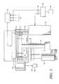
- FIG. 2is a cross-sectional diagram of an exemplary CVD plasma reactor configured for use according to the present invention
- FIG. 3is a diagram of the system monitor of the CVD plasma reactor of FIG. 2 ;
- FIG. 4is a flowchart of a process control computer program product used in conjunction with the exemplary CVD plasma reactor of FIG. 2 ;
- FIG. 5is a flow chart illustrating steps undertaken in depositing liner and cap layers in a gap filling process according to one embodiment of the present invention
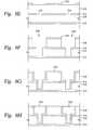
- FIG. 6A-6Eis a schematic diagram of the layers deposited on a substrate by the process of FIG. 5 ;
- FIG. 7is a cross sectional view showing a dual damascene structure comprising the silicon oxide layers of the present invention.
- FIGS. 8A-8Hare cross sectional views showing one embodiment of a dual damascene deposition sequence of the present invention.
- FIG. 9is a cross sectional view showing an adhesive layer comprising the silicon oxide layer of the present invention between a premetal dielectric layer and an intermetal dielectric layer;
- FIGS. 10A-10Hare cross sectional views showing a dual damascene deposition sequence wherein the silicon oxide of the present invention is used to adhere an intermetal dielectric film to a conventional etch stop.
- the present inventionprovides a method and apparatus for depositing a silicon oxide layer having a low dielectric constant, a high oxide content, and sufficient carbon content to provide barrier properties.
- the silicon oxide layercomprises an oxidized organosilane or organosiloxane and can be used as a lining layer adjacent other dielectric materials, as an etch stop layer adjacent dielectric materials having lower oxide content, as an intermetal dielectric layer, and as an adhesion layer between different materials.
- the oxidized organosilane materialis deposited by plasma assisted oxidation of the organosilane or organosiloxane compounds using from about 10 to about 200 W of constant RF power, or from about 20 to about 250 W of pulsed RF power.
- the constant RF power or the pulsed RF poweris preferably provided at a high frequency such as between 13 MHz and 14 MHz.
- Pulsed RF poweris preferably provided in short duration cycles wherein the power is on at the stated levels for cycles less than about 200 Hz and the on cycles total from about 10% to about 30% of the total duty cycle. Pulsed RF power can operate at higher peak power levels and provide the same total power input as constant RF power at a lower power level.
- Carbon which remains in the silicon oxide layercontributes to low dielectric constants and barrier properties.
- the remaining carbonpreferably includes sufficient C—H or C—F bonds to provide hydrophobic properties to the silicon oxide layer resulting in significantly lower dielectric constants and improved moisture barrier properties.
- the organosilane and organosiloxane compoundsgenerally include the structures: wherein each Si is bonded to one or two carbon atoms, and C is included in an organo group, preferably alkyl or alkenyl groups such as —CH 3 , —CH 2 —CH 3 , —CH 2 —, or —CH 2 —CH 2 —, or fluorinated derivatives thereof.
- the carbon atoms in the fluorinated derivativesmay be partially or fully fluorinated to replace hydrogen atoms.
- an organosilane or organosiloxane compoundincludes two or more Si atoms, each Si is separated from another Si by —O—, —C— or —C ⁇ C—, wherein C is included in an organo group, preferably alkyl or alkenyl groups such as —CH 2 —, —CH 2 —CH 2 —, —CH(CH 3 )— or —C(CH 3 ) 2 —, or fluorinated derivatives thereof.
- the preferred organosilane and organosiloxane compoundsare gases or liquids near room temperature and can be volatilized above about 10 Torr.
- Preferred organosilanes and organosiloxanesinclude:
- the hydrocarbon groups in the organosilanes and organosiloxanemay be partially or fully fluorinated to convert C—H bonds to C—F bonds.
- Many of the preferred organosilane and organosiloxane compoundsare commercially available.
- a combination of two or more of the organosilanes or organosiloxanescan be employed to provide a blend of desired properties such as dielectric constant, oxide content, hydrophobicity, film stress, and plasma etching characteristics.
- the organosilane and organosiloxane compoundsare oxidized during deposition by plasma assisted reaction with oxygen which is formed during the deposition process by decomposition of an oxygen containing compound such as nitrous oxide (N 2 O).
- Nitrous oxidedoes not react with the organosilanes or organosiloxanes without plasma assistance and the oxygen-nitrogen bonds are readily broken at lower energies than the bonds in the organosilanes and organosiloxanes.
- the oxidized compoundsadhere to contacted surfaces such as a patterned layer of a semiconductor substrate to form a deposited film.
- the deposited filmsare cured and annealed at reduced pressure and at temperatures from about 200 to about 450° C., preferably near or above about 400° C. to stabilize the barrier properties of the films.
- the deposited filmhas sufficient carbon content to provide barrier properties.
- the carbon contentpreferably includes C—H or C—F bonds to provide a hydrophobic film that is an excellent moisture barrier.
- the present inventionfurther provides a substrate processing system having a plasma reactor including a reaction zone, a substrate holder for positioning a substrate in the reaction zone, and a vacuum system.
- the processing systemfurther comprises a gas/liquid distribution system connecting the reaction zone of the vacuum chamber to supplies of an organosilane or organosiloxane compound, an oxidizing gas, and an inert gas, and an RF generator coupled to the gas distribution system for generating a plasma in the reaction zone.
- the processing systemfurther comprises a controller comprising a computer for controlling the plasma reactor, the gas distribution system, and the RF generator, and a memory coupled to the controller, the memory comprising a computer usable medium comprising a computer readable program code for selecting the process steps of depositing a low dielectric constant film with a plasma of an organosilane or organosiloxane compound and an oxidizing gas.
- the processing systemmay further comprise in one embodiment computer readable program code for selecting the process steps of depositing a liner of the oxidized organo silane compound, depositing a different dielectric layer, and optionally depositing a capping layer of the oxidized organo silane compound.
- FIG. 2is a vertical, cross-section view of a parallel plate chemical vapor deposition reactor 10 having a high vacuum region 15 .
- Reactor 10contains a gas distribution manifold 11 for dispersing process gases through perforated holes in the manifold to a substrate or wafer (not shown) that rests on a substrate support plate or susceptor 12 which is raised or lowered by a lift motor 14 .
- a liquid injection system(not shown), such as typically used for liquid injection of TEOS, may also be provided for injecting a liquid organosilane and/or organosiloxane compound.
- the preferred methylsilanesare gases.
- the reactor 10includes heating of the process gases and substrate, such as by resistive heating coils (not shown) or external lamps (not shown).
- susceptor 12is mounted on a support stem 13 so that susceptor 12 (and the wafer supported on the upper surface of susceptor 12 ) can be controllably moved between a lower loading/off-loading position and an upper processing position which is closely adjacent to manifold 11 .
- susceptor 12 and the waferWhen susceptor 12 and the wafer are in processing position 14 , they are surrounded by an insulator 17 and process gases exhaust into a manifold 24 . During processing, gases inlet to manifold 11 are uniformly distributed radially across the surface of the wafer.
- a vacuum pump 32 having a throttle valvecontrols the exhaust rate of gases from the chamber.
- deposition and carrier gasesare input through gas lines 18 into a mixing system 19 where they are combined and then sent to manifold 11 .
- the process gases supply lines 18 for each of the process gasesinclude (i) safety shut-off valves (not shown) that can be used to automatically or manually shut off the flow of process gas into the chamber, and (ii) mass flow controllers (also not shown) that measure the flow of gas through the gas supply lines.
- safety shut-off valvesnot shown
- mass flow controllersalso not shown
- the deposition process performed in reactor 10can be either a thermal process or a plasma enhanced process.
- a controlled plasmais typically formed adjacent to the wafer by RF energy applied to distribution manifold 11 from RF power supply 25 (with susceptor 12 grounded).
- RF powercan be provided to the susceptor 12 or RF power can be provided to different components at different frequencies.
- RF power supply 25can supply either single or mixed frequency RF power to enhance the decomposition of reactive species introduced into the high vacuum region 15 .
- a mixed frequency RF power supplytypically supplies power at a high RF frequency (RF1) of 13.56 MHz to the distribution manifold 11 and at a low RF frequency (RF2) of 360 KHz to the susceptor 12 .
- the silicon oxide layers of the present inventionare most preferably produced using low levels of constant high frequency RF power or pulsed levels of high frequency RF power.
- Pulsed RF powerpreferably provides 13.56 MHz RF power at about 20 to about 250 W, most preferably from 20 to 150 W, during about 10 to about 30% of the duty cycle.
- Constant RF powerpreferably provides 13.56 MHz RF power at about 10 to about 200 W, preferably from 20 to 100 W.
- Low power depositionpreferably occurs at a temperature range from about ⁇ 20 to about 40° C. At the preferred temperature range, the deposited film is partially polymerized during deposition and polymerization is completed during subsequent curing of the film.
- any or all of the chamber lining, gas inlet manifold faceplate, support stem 13 , and various other reactor hardwareis made out of material such as aluminum or anodized aluminum.
- An example of such a CVD reactoris described in U.S. Pat. No. 5,000,113, entitled “Thermal CVD/PECVD Reactor and Use for Thermal Chemical Vapor Deposition of Silicon Dioxide and In-situ Multi-step Planarized Process,” issued to Wang et al. And assigned to Applied Materials, Inc., the assignee of the present invention.
- the lift motor 14raises and lowers susceptor 12 between a processing position and a lower, wafer-loading position.
- the motor, the gas mixing system 19 , and the RF power supply 25are controlled by a system controller 34 over control lines 36 .
- the reactorincludes analog assemblies, such as mass flow controllers (MFCs) and standard or pulsed RF generators, that are controlled by the system controller 34 which executes system control software stored in a memory 38 , which in the preferred embodiment is a hard disk drive.
- MFCsmass flow controllers
- RF generatorssystem control software stored in a memory 38 , which in the preferred embodiment is a hard disk drive.
- Motors and optical sensorsare used to move and determine the position of movable mechanical assemblies such as the throttle valve of the vacuum pump 32 and motor for positioning the susceptor 12 .
- the system controller 34controls all of the activities of the CVD reactor and a preferred embodiment of the controller 34 includes a hard disk drive, a floppy disk drive, and a card rack.
- the card rackcontains a single board computer (SBC), analog and digital input/output boards, interface boards and stepper motor controller boards.
- SBCsingle board computer
- the system controllerconforms to the Versa Modular Europeans (VME) standard which defines board, card cage, and connector dimensions and types.
- VMEVersa Modular Europeans
- the VME standardalso defines the bus structure having a 16-bit data but and 24-bit address bus.
- the system controller 34operates under the control of a computer program stored on the hard disk drive 38 .
- the computer programdictates the timing, mixture of gases, RF power levels, susceptor position, and other parameters of a particular process.
- the interface between a user and the system controlleris via a CRT monitor 40 and light pen 44 which are depicted in FIG. 3 .
- a second monitor 42is used, the first monitor 40 being mounted in the clean room wall for the operators and the other monitor 42 behind the wall for the service technicians. Both monitors 40 , 42 simultaneously display the same information but only one light pen 44 is enabled.
- the light pen 44detects light emitted by CRT display with a light sensor in the tip of the pen.
- the operatortouches a designated area of the display screen and pushes the button on the pen 44 .
- the touched areachanges its highlighted color, or a new menu or screen is displayed, confirming communication between the light pen and the display screen.
- the processcan be implemented using a computer program product 410 that runs on, for example, the system controller 34 .
- the computer program codecan be written in any conventional computer readable programming language such as for example 68000 assembly language, C, C++, or Pascal. Suitable program code is entered into a single file, or multiple files, using a conventional text editor, and stored or embodied in a computer usable medium, such as a memory system of the computer. If the entered code text is in a high level language, the code is compiled, and the resultant compiler code is then linked with an object code of precompiled windows library routines. To execute the linked compiled object code, the system user invokes the object code, causing the computer system to load the code in memory, from which the CPU reads and executes the code to perform the tasks identified in the program.
- FIG. 4shows an illustrative block diagram of the hierarchical control structure of the computer program 410 .
- a userenters a process set number and process chamber number into a process selector subroutine 420 in response to menus or screens displayed on the CRT monitor 40 by using the light pen 44 interface.
- the process setsare predetermined sets of process parameters necessary to carry out specified processes, and are identified by predefined set numbers.
- the process selector subroutine 420the (i) selects a desired process chamber on a cluster tool such as an CenturaTM platform (available from Applied Materials, Inc.), and (ii) selects a desired set of process parameters needed to operate the process chamber for performing the desired process.
- the process parameters for performing a specific processrelate to process conditions such as, for example, process gas composition and flow rates, temperature, pressure, plasma conditions such as RF bias power levels and magnetic field power levels, cooling gas pressure, and chamber wall temperature and are provided to the user in the form of a recipe.
- process conditionssuch as, for example, process gas composition and flow rates, temperature, pressure, plasma conditions such as RF bias power levels and magnetic field power levels, cooling gas pressure, and chamber wall temperature and are provided to the user in the form of a recipe.
- the parameters specified by the recipeare entered utilizing the light pen/CRT monitor interface.
- the signals for monitoring the processare provided by the analog input and digital input boards of system controller and the signals for controlling the process are output on the analog output and digital output boards of the system controller 34 .
- a process sequencer subroutine 430comprises program code for accepting the identified process chamber and set of process parameters from the process selector subroutine 420 , and for controlling operation of the various process chambers. Multiple users can enter process set numbers and process chamber numbers, or a user can enter multiple process chamber numbers, so the sequencer subroutine 430 operates to schedule the selected processes in the desired sequence.
- the sequencer subroutine 430includes computer readable program code to perform the steps of (i) monitoring the operation of the process chambers to determine if the chambers are being used, (ii) determining what processes are being carried out in the chambers being used, and (iii) executing the desired process based on availability of a process chamber and type of process to be carried out.
- sequencer subroutine 430can be designed to take into consideration the present condition of the process chamber being used in comparison with the desired process conditions for a selected process, or the “age” of each particular user entered request, or any other relevant factor a system programmer desires to include for determining the scheduling priorities.
- the sequencer subroutine 430determines which process chamber and process set combination is going to be executed next, the sequencer subroutine 430 causes execution of the process set by passing the particular process set parameters to a chamber manager subroutine 440 which controls multiple processing tasks in a process chamber 10 according to the process set determined by the sequencer subroutine 430 .
- the chamber manager subroutine 440comprises program code for controlling CVD process operations in the process chamber 10 .
- the chamber manager subroutine 440also controls execution of various chamber component subroutines which control operation of the chamber component necessary to carry out the selected process set.
- chamber component subroutinesare susceptor control subroutine 450 , process gas control subroutine 460 , pressure control subroutine 470 , heater control subroutine 480 , and plasma control subroutine 490 .
- process gas control subroutine 460processes gas control subroutine 460
- pressure control subroutine 470pressure control subroutine 470
- heater control subroutine 480heater control subroutine 490 .
- plasma control subroutine 490examples of chamber component subroutines.
- the chamber manager subroutine 440selectively schedules or calls the process component subroutines in accordance with the particular process set being executed.
- the chamber manager subroutine 440schedules the process component subroutines similarly to how the sequencer subroutine 430 schedules which process chamber 10 and process set is to be executed next.
- the chamber manager subroutine 440includes steps of monitoring the various chamber components, determining which components needs to be operated based on the process parameters for the process set to be executed, and causing execution of a chamber component subroutine responsive to the monitoring and determining steps.
- the susceptor control positioning subroutine 450comprises program code for controlling chamber components that are used to load the substrate onto the susceptor 12 , and optionally to lift the substrate to a desired height in the reactor 10 to control the spacing between the substrate and the gas distribution manifold 11 .
- the susceptor 12is lowered to receive the substrate, and thereafter, the susceptor 12 is raised to the desired height in the chamber, to maintain the substrate at a first distance or spacing from the gas distribution manifold 11 during the CVD process.
- the susceptor control subroutine 450controls movement of the susceptor 12 in response to process set parameters that are transferred from the chamber manager subroutine 440 .
- the process gas control subroutine 460has program code for controlling process gas composition and flow rates.
- the process gas control subroutine 460controls the open/close position of the safety shut-off valves, and also ramps up/down the mass flow controllers to obtain the desired gas flow rate.
- the process gas control subroutine 460is invoked by the chamber manager subroutine 440 , as are all chamber components subroutines, and receives from the chamber manager subroutine process parameters related to the desired gas flow rates.
- the process gas control subroutine 460operates by opening the gas supply lines, and repeatedly (i) reading the necessary mass flow controllers, (ii) comparing the readings to the desired flow rates received from the chamber manager subroutine 440 , and (iii) adjusting the flow rates of the gas supply lines as necessary. Furthermore, the process gas control subroutine 460 includes steps for monitoring the gas flow rates for unsafe rates, and activating the safety shut-off valves when an unsafe condition is detected.
- an inert gassuch as helium or argon is flowed into the reactor 10 to stabilize the pressure in the chamber before reactive process gases are introduced into the chamber.
- the process gas control subroutine 460is programmed to include steps for flowing the inert gas into the chamber 10 for an amount of time necessary to stabilize the pressure in the chamber, and then the steps described above would be carried out.
- a process gasis to be vaporized from a liquid precursor, for example 1,3,5-trisilano-2,4,6-trimethylene (1,3,5-trisilanacyclo-hexane)
- the process gas control subroutine 460would be written to include steps for bubbling a delivery gas such as helium through the liquid precursor in a bubbler assembly.
- the process gas control subroutine 460regulates the flow of the delivery gas, the pressure in the bubbler, and the bubbler temperature in order to obtain the desired process gas flow rates.
- the desired process gas flow ratesare transferred to the process gas control subroutine 460 as process parameters.
- the process gas control subroutine 460includes steps for obtaining the necessary delivery gas flow rate, bubbler pressure, and bubbler temperature for the desired process gas flow rate by accessing a stored table containing the necessary values for a given process gas flow rate. Once the necessary values are obtained, the delivery gas flow rate, bubbler pressure and bubbler temperature are monitored, compared to the necessary values and adjusted accordingly.
- the pressure control subroutine 470comprises program code for controlling the pressure in the reactor 10 by regulating the size of the opening of the throttle valve in the exhaust pump 32 .
- the size of the opening of the throttle valveis set to control the chamber pressure to the desired level in relation to the total process gas flow, size of the process chamber, and pumping set point pressure for the exhaust pump 32 .
- the pressure control subroutine 470is invoked, the desired, or target pressure level is received as a parameter from the chamber manager subroutine 440 .
- the pressure control subroutine 470operates to measure the pressure in the reactor 10 by reading one or more conventional pressure manometers connected to the chamber, compare the measure value(s) to the target pressure, obtain PID (proportional, integral, and differential) values from a stored pressure table corresponding to the target pressure, and adjust the throttle valve according to the PID values obtained from the pressure table.
- the pressure control subroutine 470can be written to open or close the throttle valve to a particular opening size to regulate the reactor 10 to the desired pressure.
- the heater control subroutine 480comprises program code for controlling the temperature of the heat modules or radiated heat that is used to heat the susceptor 12 .
- the heater control subroutine 480is also invoked by the chamber manager subroutine 440 and receives a target, or set point, temperature parameter.
- the heater control subroutine 480measures the temperature by measuring voltage output of a thermocouple located in a susceptor 12 , compares the measured temperature to the set point temperature, and increases or decreases current applied to the heat module to obtain the set point temperature.
- the temperatureis obtained from the measured voltage by looking up the corresponding temperature in a stored conversion table, or by calculating the temperature using a fourth order polynomial.
- the heater control subroutine 480gradually controls a ramp up/down of current applied to the heat module. The gradual ramp up/down increases the life and reliability of the heat module. Additionally, a built-in-fail-safe mode can be included to detect process safety compliance, and can shut down operation of the heat module if the reactor 10 is not properly set up.
- the plasma control subroutine 490comprises program code for setting the RF bias voltage power level applied to the process electrodes in the reactor 10 , and optionally, to set the level of the magnetic field generated in the reactor. Similar to the previously described chamber component subroutines, the plasma control subroutine 490 is invoked by the chamber manager subroutine 440 .
- CVD system descriptionis mainly for illustrative purposes, and other plasma CVD equipment such as electrode cyclotron resonance (ECR) plasma CVD devices, induction-coupled RF high density plasma CVD devices, or the like may be employed. Additionally, variations of the above described system such as variations in susceptor design, heater design, location of RF power connections and others are possible. For example, the wafer could be supported and heated by a resistively heated susceptor.
- ECRelectrode cyclotron resonance
- the pretreatment and method for forming a pretreated layer of the present inventionis not limited to any specific apparatus or to any specific plasma excitation method.
- the oxidized organosilane or organosiloxane layer of the present inventioncan be used in a three-layer gap filling process as shown in FIG. 5 using the PECVD chamber of FIG. 2 .
- a waferis positioned 200 in the reactor 10 and an oxidized organosilane layer having a low dielectric constant is deposited 205 by a PECVD process from a plasma comprising an organosilane compound and/or a organosiloxane compound.
- the deposition step 205can include a capacitively coupled plasma or both an inductively and a capacitively coupled plasma in the process chamber 15 according to methods known in the art.
- a gap fill layeris then deposited 210 on the liner layer by known methods.
- the gap fill layeris preferably self-planarizing, such as spin-on polymers or oxides deposited in liquid form by reaction of methyl silane and hydrogen peroxide.
- a cap layeris then deposited 215 on the gap fill layer, preferably using the same process for depositing the lining layer. The wafer is then removed 220 from the reactor 10 .
- the three-layer gap filling processprovides a PECVD lining layer 300 of the oxidized organosilane or organosiloxane polymer.
- the lining layer 300acts as an isolation layer between a subsequent gap fill layer 302 and the underlying substrate surface 304 and metal lines 306 , 308 , 310 formed on the substrate surface.
- the gap fill layer 302is capped by a PECVD capping layer 312 of the oxidized organosilane or organosiloxane polymer. This process is implemented and controlled using a computer program stored in the memory 38 of a computer controller 34 for a CVD reactor 10 .
- the PECVD lining layer 300is deposited in the reactor 10 by introducing an oxidizing gas such as N 2 O, an organosilane or organosiloxane compound such as CH 3 SiH 3 or (CH 3 ) 2 SiH 2 , and a carrier gas such as helium.
- the substrateis maintained at a temperature of from about ⁇ 20 to about 400° C., and preferably is maintained at a temperature of approximately ⁇ 20 to 40° C. throughout the deposition of the PECVD lining layer.
- the PECVD lining layer 300is deposited with a process gas that includes a mixture of the organosilane and/or organosiloxane compound at a flow rate of about 5 sccm to about 500 sccm and the oxidizing gas at a flow rate of about 5 sccm to about 2000 sccm.
- the process gasesare carried by an inert gas such He, Ar, Ne, or a relatively inert gas such as nitrogen, which are typically not incorporated into the film, at a flow rate of from about 0.2 to about 20 Ipm.
- the process gasesreact at a pressure from about 0.2 to about 20 Torr, preferably less than 10 Torr, to form a conformal silicon oxide layer on the substrate surface 304 and metal lines 306 , 308 , 310 .
- the reactionis plasma enhanced with a power density ranging from 0.05 W/cm 2 to 1000 W/cm 2 , preferably a power density less than about 1 W/cm 2 , most preferably a power density ranging from about 0.1 to about 0.3 W/cm 2 .
- the high frequency RF source of approximately 13.56 MHzis preferably connected to a gas distribution system and driven at about 10 to about 250 W while a low frequency RF source of about 350 KHz to 1 MHz is optionally connected to a susceptor and driven at about 0 to about 100 W.
- the high frequency RF sourceis driven at about 20-150 W of pulsed RF power and the low frequency RF source is driven at about 0-50 W of pulsed RF power at a duty cycle from 10% to 30%.
- the pulsed RF poweris rapidly cycled in short intervals, preferably having a frequency less than about 200 Hz.
- the power levelpreferably ranges from about 20 W to about 100 W.
- the oxidized organosilane or organosiloxane layeris then annealed at a pressure less than the deposition pressure and a temperature from about 200 to about 450° C.
- annealingcould be conducted after deposition of additional dielectric layers.
- the above process conditionsresult in the deposition of a PECVD lining layer 300 (at about 2000 ⁇ per minute) with improved barrier characteristics for the subsequent deposition of the gap filling layer 302 shown in — FIG. 6B .
- the lining layer obtained from methylsilanehas sufficient C—H bonds to be hydrophobic, and is an excellent moisture barrier.
- Deposition of a hydrophobic lining layerhas a surprising and unexpected result of converting subsequent hydrophilic layers to hydrophobic layers.
- the process gases for the gap filling layer 302are preferably SiH 4 , or CH 3 SiH 3 , and 50 wt % of hydrogen peroxide (H 2 O 2 ) which is vaporized and mixed with an inert carrier gas, such as helium.
- the gap filling layercan be any dielectric layer which has an acceptable dielectric constant.
- Alternative silicon containing compoundscan be used if byproducts are vapors at deposition conditions.
- Preferred alternative compoundsincorporate oxysilano or silano groups, such as:
- the process gas flowsrange from 0-2000 sccm for He, 10-200 sccm for CH 3 SiH 3 , and 0.1 to 3 g/min. for H 2 O 2 .
- the preferred gas flowsrange from 100-500 scorn for He, 20-100 sccm for CH 3 SiH 3 , and 0.1 to 1 g/min. for H 2 O 2 . These flow rates are given for a chamber having a volume of approximately 5.5 to 6.5 liters.
- reactor 10is maintained at a pressure of about 0.2 to about 5 torr during deposition of the gap filling layer 302 .
- the gap filling layer 302may be partially cured as shown in FIG. 6C to remove solvents such as water prior to deposition of a cap layer 312 as shown in FIG. 6D . Curing is done in the reactor 10 by pumping under an inert gas atmosphere under 10 Torr.
- Gap filling layers produced from methylsilaneare typically hydrophilic and have poor moisture barrier properties.
- a gap filling layer produced from methylsilaneWhen deposited on a lining layer produced from methylsilane, a gap filling layer produced from methylsilane surprisingly is hydrophobic and has good moisture barrier properties.
- the reactor 10optionally resumes deposition of the oxidized organosilane or organosiloxane layer of the present invention for deposition of a capping layer 312 .
- the deposited layersare annealed in a furnace or another chamber at a temperature from about 100 to about 450° C. to drive off remaining solvent such as water.
- processing conditionswill vary according to the desired characteristics of the deposited films.
- a dual damascene structure which includes an oxidized organosilane or organosiloxane layers as an etch stop or as an intermetal dielectric layeris shown in FIG. 7 .
- a first dielectric layer 510is deposited on a substrate 512 and then the oxidized organosilane or organosiloxane etch stop 514 is deposited on the first dielectric layer and annealed.
- the etch stopis then pattern etched to define the openings of the contacts/vias 516 .
- a second dielectric layer 518is then deposited over the patterned etch stop and then pattern etched by conventional methods to define the interconnect lines 520 .
- a single etch processis then performed to define the interconnects down to the etch stop and to etch the unprotected dielectric exposed by the patterned etch stop to define the contacts/vias.
- the damascene structurealternatively includes the oxidized organosilane or organsiloxane as an intermetal dielectric.
- a first dielectric layer 510preferably consisting of the oxidized organosilane or organosiloxane, is deposited on a substrate 512 and then a conventional silicon oxide, silicon nitride, or hydrogenated silicon carbide etch stop 514 is deposited on the first dielectric layer. The etch stop is then patterned to define the openings of the contacts/vias 516 .
- a second dielectric layer 518consisting of the oxidized organosilane or organosiloxane, is then deposited over the patterned etch stop and then patterned to define the interconnect lines 520 .
- a single etch processis then performed to define the interconnects down to the etch stop and to etch the unprotected dielectric exposed by the patterned etch stop to define the contacts/vias.
- a preferred dual damascene structure fabricated in accordance with the inventionincludes a lining layer as shown in FIG. 8H , and the method of making the structure is sequentially depicted schematically in FIGS. 8A-8H , which are cross sectional views of a substrate having the steps of the invention formed thereon.
- an initial first dielectric layer 510such as parylene, FSG, silicon oxide, or the like, is deposited on the substrate 512 to a thickness of about 5,000 to about 10,000 ⁇ , depending on the size of the structure to be fabricated.
- the low k etch stop 514which is the oxidized organosilane or organosiloxane layer, is then deposited on the first dielectric layer to a thickness of about 200 to about 1000 ⁇ using low levels of RF power.
- the low k etch stop 514is then pattern etched to define the contact/via openings 516 and to expose first dielectric layer 510 in the areas where the contacts/vias are to be formed as shown in FIG.
- low k etch stop 514is pattern etched using conventional photolithography and etch processes using fluorine, carbon, and oxygen ions.
- a second dielectric layer 518is deposited over etch stop 514 to a thickness of about 5,000 to about 10,000 ⁇ as shown in FIG. 8D .
- a second dielectric layer 518is then patterned to define interconnect lines 520 , preferably using conventional photolithography processes with a photo resist layer 522 as shown in FIG. 8E .
- interconnects and contacts/viasare then etched using reactive ion etching or other anisotropic etching techniques to define the metallization structure (i.e., the interconnect and contact/via) as shown in FIG. 8 f .
- Any photo resist or other material used to pattern the etch stop 514 or the second dielectric layer 518is removed using an oxygen strip or other suitable process.
- the metallization structureis then formed with a conductive material such as aluminum, copper, tungsten or combinations thereof.
- a conductive materialsuch as aluminum, copper, tungsten or combinations thereof.
- the trendis to use copper to form the smaller features due to the low resistivity of copper (1.7 ⁇ -cm compared to 3.1 ⁇ -cm for aluminum).
- a suitable barrier layer 524such as tantalum nitride is first deposited conformally in the metallization pattern to prevent copper migration into the surrounding silicon and/or dielectric material. Thereafter, copper is deposited using either chemical vapor deposition, physical vapor deposition, electroplating, or combinations thereof to form the conductive structure.
- the surfaceis planarized using chemical mechanical polishing, as shown in FIG. 8H .
- a dual damascene structurewhich includes an oxidized organosilane or organosiloxane layer as an adhesive layer between a premetal dielectric layer and an intermetal dielectric layer is shown in FIG. 9 .
- the oxidized organosilane or organosiloxane adhesive layer 612is deposited on a premetal dielectric layer 610 such as a conventional PSG or BPSG layer and then annealed.
- An intermetal dielectric layer 614preferably a low k dielectric polymer layer, is then deposited over the adhesive layer 612 .
- a conventional silicon oxide or silicon nitride etch stop 616and then patterned by conventional methods to define vias 620 .
- a second intermetal dielectric layer 622preferably the low k dielectric polymer, is then deposited over the patterned etch stop and then patterned to define the interconnect lines.
- a single etch processis then performed to define the interconnects down to the etch stop and to etch the unprotected dielectric exposed by the patterned etch stop to define the contacts/vias prior to metallization.
- FIG. 10HA preferred dual damascene structure comprising an adhesive layer in accordance with the invention is shown in FIG. 10H , and the method of making the structure is sequentially depicted schematically in FIGS. 10A-10H , which are cross sectional views of a substrate having the steps of the invention formed thereon.
- an initial first intermetal dielectric layer 710such as parylene, FSG, silicon oxide, or the like, is deposited on a substrate 712 to a thickness of about 5,000 to about 10,000 ⁇ , depending on the size of the structure to be fabricated.
- a low k adhesive layer 714which is the oxidized organo silane layer, is then deposited on the first intermetal dielectric layer 710 to a thickness of about 50 to about 200 ⁇ .
- a conventional silicon oxide or silicon nitride etch stop 716is the deposited on the adhesive layer 714 to a thickness of about 50 to about 200 ⁇ .
- a second low k adhesive layer 718which is the oxidized organo silane layer, is then deposited on the etch stop 716 to a thickness of about 50 to about 200 ⁇ .
- the etch stop 716 and adhesive layers 714 , 718are then pattern etched to define the contact/via openings 720 and to expose first intermetal dielectric layer 710 in the areas where the contacts/vias are to be formed as shown in FIG. 10C .
- the etch stop 716is pattern etched using conventional photolithography and etch processes using fluorine, carbon, and oxygen ions.
- a second intermetal dielectric layer 722is deposited over second adhesive layer 718 to a thickness of about 5;000 to about 10,000 ⁇ as shown in FIG. 10D .
- the second intermetal dielectric layer 722is then patterned to define interconnect lines 724 , preferably using conventional photolithography processes with a photo resist layer 726 as shown in FIG. 10E .
- the interconnects and contacts/viasare then etched using reactive ion etching or other anisotropic etching techniques to define the metallization structure (i.e., the interconnect and contact/via) as shown in FIG. 10F .
- Any photo resist or other material used to pattern the etch stop 716 or the second intermetal dielectric layer 722is removed using an oxygen strip or other suitable process.
- the metallization structureis then formed with a conductive material such as aluminum, copper, tungsten or combinations thereof.
- a conductive materialsuch as aluminum, copper, tungsten or combinations thereof.
- the trendis to use copper to form the smaller features due to the low resistivity of copper (1.7 ⁇ -cm compared to 3.1 ⁇ -cm for aluminum).
- a suitable barrier layer 728such as tantalum nitride is first deposited conformally in the metallization pattern to prevent copper migration into the surrounding silicon and/or dielectric material. Thereafter, copper is deposited using either chemical vapor deposition, physical vapor deposition, electroplating, or combinations thereof to form the conductive structure.
- the surfaceis planarized using chemical mechanical polishing, as shown in FIG. 10H .
- the following examplesdemonstrate deposition of an oxidized organosilane or organosiloxane film having excellent barrier and adhesion properties.
- This examplewas undertaken using a chemical vapor deposition chamber, and in particular, a “CENTURA DxZ” system which includes a solid-state RF matching unit with a two-piece quartz process kit, both fabricated and sold by Applied Materials, Inc., Santa Clara, Calif.
- An oxidized dimethylsilane filmwas deposited at a chamber pressure of 3.0 Torr and temperature of 15° C. from reactive gases which were flowed into the reactor as follows: Dimethylsilane, (CH 3 ) 2 SiH 2 , att 55 sccm Nitrous oxide, N 2 O, at 300 sccm Helium, He, at 4000 sccm.
- the substratewas positioned 600 mil from the gas distribution showerhead and 20 W of high frequency power (13 MHz) was applied to the showerhead for plasma enhanced deposition of an oxidized dimethylsilane layer.
- the oxidized dimethylsilane materialhad a dielectric constant of about 2.5 and was hydrophobic. Pulsed RF Power (Hypothetical)
- An oxidized 1,3,5-trisilano-2,4,6-trimethylene (cyclic) filmis deposited at a chamber pressure of 3.0 Torr and temperature of 15° C. from reactive gases which flow into the reactor as follows: 1,3,5-trisilano-2,4,6-trimethylene, -(-SiH 2 CH 2 -) 3 - 20 sccm (cyclic), at Nitrous oxide, N 2 O, at 300 sccm Helium, He, at 4000 sccm.
- the substrateis positioned 600 mil from the gas distribution showerhead and 50 W of pulsed high frequency power (13 MHz) is applied to the showerhead for plasma enhanced deposition of an oxidized 1,3,5-trisilano-2,4,6-trimethylene layer.
- Pulsed RF Power(Hypothetical)
- An oxidized 1,3-dimethyldisiloxane filmis deposited at a chamber pressure of 3.0 Torr and temperature of 15° C. from reactive gases which are flowed into the reactor as follows: 1,3-Dimethyldisiloxane, CH 3 —SiH 2 —O—SiH 2 —CH 3 , at 30 sccm Nitrous oxide, N 2 O, at 300 sccm Helium, He, at 4000 sccm.
- the substrateis positioned 600 mil from the gas distribution showerhead and 50 W of pulsed high frequency power (13 MHz) is applied to the showerhead for plasma enhanced deposition of an oxidized dimethyldisiloxane layer.
Landscapes
- Engineering & Computer Science (AREA)
- Physics & Mathematics (AREA)
- Condensed Matter Physics & Semiconductors (AREA)
- General Physics & Mathematics (AREA)
- Manufacturing & Machinery (AREA)
- Computer Hardware Design (AREA)
- Microelectronics & Electronic Packaging (AREA)
- Power Engineering (AREA)
- Chemical & Material Sciences (AREA)
- Chemical Kinetics & Catalysis (AREA)
- Inorganic Chemistry (AREA)
- General Chemical & Material Sciences (AREA)
- Materials Engineering (AREA)
- Mechanical Engineering (AREA)
- Metallurgy (AREA)
- Organic Chemistry (AREA)
- Formation Of Insulating Films (AREA)
- Internal Circuitry In Semiconductor Integrated Circuit Devices (AREA)
- Chemical Vapour Deposition (AREA)
Abstract
Description
- This application is a continuation of co-pending U.S. patent application Ser. No. 10/322,212, filed Dec. 17, 2002, now issued as U.S. Pat. No. 6,800,571, which is a continuation of U.S. patent application Ser. No. 09/580,505, filed May 25, 2000, now issued as U.S. Pat. No. 6,537,929, which is a continuation of U.S. patent application Ser. No. 09/162,915, filed Sep. 29, 1998, now issued as U.S. Pat. No. 6,287,990.
- 1. Field of the Invention
- The present invention relates to the fabrication of integrated circuits. More particularly, the invention relates to a process and apparatus for depositing dielectric layers on a substrate.
- 2. Background of the Invention
- One of the primary steps in the fabrication of modern semiconductor devices is the formation of metal and dielectric films on a substrate by chemical reaction of gases. Such deposition processes are referred to as chemical vapor deposition or CVD. Conventional thermal CVD processes supply reactive gases to the substrate surface where heat-induced chemical reactions take place to produce a desired film. The high temperatures at which some thermal CVD processes operate can damage device structures having layers previously formed on the substrate. A preferred method of depositing metal and dielectric films at relatively low temperatures is plasma-enhanced CVD (PECVD) techniques such as described in U.S. Pat. No. 5,362,526, entitled “Plasma-Enhanced CVD Process Using TEOS for Depositing Silicon Oxide”, which is incorporated by reference herein. Plasma-enhanced CVD techniques promote excitation and/or disassociation of the reactant gases by the application of radio frequency (RF) energy to a reaction zone near the substrate surface, thereby creating a plasma of highly reactive species. The high reactivity of the released species reduces the energy required for a chemical reaction to take place, and thus lowers the required temperature for such PECVD processes.
- Semiconductor device geometries have dramatically decreased in size since such devices were first introduced several decades ago. Since then, integrated circuits have generally followed the two year/half-size rule (often called Moore's Law), which means that the number of devices that will fit on a chip doubles every two years. Today's fabrication plants are routinely producing devices having 0.35 μm and even 0.18 μm feature sizes, and tomorrow's plants soon will be producing devices having even smaller geometries.
- In order to further reduce the size of devices on integrated circuits, it has become necessary to use conductive materials having low resistivity and insulators having low k (dielectric constant <4.0) to reduce the capacitive coupling between adjacent metal lines. Liner/barrier layers have been used between the conductive materials and the insulators to prevent diffusion of byproducts such as moisture onto the conductive material as described in International Publication Number WO 94/01885. For example, moisture that can be generated during formation of a low k insulator readily diffuses to the surface of the conductive metal and increases the resistivity of the conductive metal surface. A barrier/liner layer formed from conventional silicon oxide or silicon nitride materials can block the diffusion of the byproducts. However, the barrier/liner layers typically have dielectric constants that are significantly greater than 4.0, and the high dielectric constants result in a combined insulator that does not significantly reduce the dielectric constant.
FIG. 1A illustrates a PECVD process for depositing a barrier/liner layer as described in International Publication Number WO 94/01885. The PECVD process deposits a multi-component dielectric layer wherein a silicon dioxide (SiO2)liner layer 2 is first deposited on a patterned metal layer havingmetal lines 3 formed on asubstrate 4. Theliner layer 2 is deposited by a plasma enhanced reaction of silane (SiH4) and nitrous oxide (N2O) at 300° C. A self-planarizing low kdielectric layer 5 is then deposited on theliner layer 2 by reaction of a silane compound and a peroxide compound. The self-planarizinglayer 5 retains moisture that is removed by annealing. Theliner layer 2 is an oxidized silane film that has effective barrier properties when deposited in a manner which provides a dielectric constant of at least 4.5. The dielectric constant of the oxidized silane film can be decreased to about 4.1 by altering process conditions in a manner that decreases moisture barrier properties of the film. Conventional liner layers, such as SiN, have even higher dielectric constants, and the combination of low k dielectric layers with high k dielectric liner layers can provide little or no improvement in the overall stack dielectric constant and capacitive coupling.- As shown in
FIG. 1B , WO 94/01885 further describes an optional SiO2cap layer6 that is deposited on the low kdielectric layer 5 by the reaction of silane and N2O. Thecap layer 6 is also an oxidized silane film that has good barrier properties when deposited in a manner that provides a dielectric constant of about 4.5. Both theliner layer 2 and thecap layer 6 have a dielectric constant greater than 4.5 and the high dielectric constant layers substantially detract from the benefit of the low kdielectric layer 5. - As devices get smaller, liner layers and cap layers having high dielectric constants contribute more to the overall dielectric constant of a multi-component dielectric layer. Furthermore, known low k dielectric materials generally have low oxide content which makes the material inadequate as an etch stop layer during etching of vias and/or interconnects. Silicon nitride has been the etch stop material of choice for making interconnect lines in low k dielectric materials. However, the silicon nitride has a relatively high dielectric constant (dielectric constant of about 7) compared to the surrounding low k dielectric layers. It has also been discovered that the silicon nitride may significantly increase the capacitive coupling between interconnect lines, even when an otherwise low k dielectric material is used as the primary insulator. This may lead to crosstalk and/or resistance-capacitance (RC) delay that degrades the overall performance of the device. Thus, the silicon nitride etch stop layers are typically removed after etching of the underlying dielectric layers.
- Ideally, a low k dielectric layer having both good barrier properties for use as a liner layer and sufficient oxide content for use as an etch stop could be identified and deposited in the same chambers as existing low k dielectric materials. Such barrier layers would not increase the overall dielectric constant of the dielectric layers, and such an etch stop layer would not have to be removed after etching the underlying layers.
- U.S. Pat. No. 5,554,570 describes barrier layers for use with thermal CVD silicon oxides wherein an organosilane having a C—H group is oxidized instead of silane to increase the density of deposited films and to improve adhesion between the layers. For example, a thermal CVD layer produced from tetraethoxysilane (TEOS) and ozone, may be deposited between PECVD silicon oxide films produced from an organosilane and N2O or O2.
- The barrier layers described in the '570 patent are preferably dense silicon oxide layers having low carbon contents. The dense layers are deposited using 400 W of high frequency RF power although the use of low frequency RF power is asserted to improve film stress. The barrier layers are preferably produced from alkoxysilanes or chlorinated alkylsilanes and N2O to reduce carbon content and increase the density of the layers.
- The '570 patent does not identify process conditions for making barrier layers having low dielectric constants or for making etch stop layers having high oxide contents. The '570 patent also does not suggest use of the described layers as a barrier layer adjacent a low k dielectric layer or as an etch stop.
- There remains a need for dielectric layers having low dielectric constants, good barrier properties, and high oxide content for use as barrier layers or etch stop layers in sub-micron devices.
- The present invention provides a method and apparatus for depositing a silicon oxide layer having a low dielectric constant, sufficient oxygen content for use as an etch stop layer, and some hydrogenated or fluorinated carbon content to impart hydrophobic properties. The silicon oxide layer is produced by plasma assisted chemical vapor deposition of an organosilane, an organosiloxane, or combinations thereof, using low RF power levels to generate reactive oxygen atoms. The silicon oxide layers have excellent barrier properties for use as a liner or cap layer adjacent other dielectric layers such as self-planarizing low k dielectric layers. In addition, the silicon oxide layers can be used as an adhesive layer between different layers, or as an intermetal dielectric layer. A preferred silicon oxide layer is produced by reaction of nitrous oxide, N2O, and methylsilane, CH3SiH3, or dimethylsilane, (CH3)2SiH2, and using from about 10 to about 250 W of high frequency RF power. The layers are annealed at low pressure and high temperature to stabilize properties.
- The silicon oxide layers of the present invention are most preferably produced using low levels of constant RF power or pulsed levels of RF power at chamber pressures less than about 10 Torr. Pulsed RF power provides high frequency RF power at about 20 to about 250 W during about 10 to about 30% of the duty cycle. Constant RF power provides high frequency RF power at about 10 to about 200 W. Low power deposition preferably occurs at a temperature range from about −20 to about 40° C. At the preferred temperature range, the deposited film is partially polymerized during deposition and polymerization is completed during subsequent curing of the film.
- In a preferred embodiment, a silicon oxide layer is deposited on a patterned metal layer by plasma assisted reaction of one or more organosilane and/or organosiloxane compounds and nitrous oxide using low levels of constant RF power. A self-planarizing dielectric layer is then deposited in the same chamber by reaction of a silicon compound such as methysilane or silane and a peroxide compound such as hydrogen peroxide in the absence of RF power. The self-planarizing dielectric layer is optionally capped in the same chamber by further reaction of the organosilane and/or organosiloxane compound and nitrous oxide using low levels of constant RF power. The liner and cap layers provide strength to the self-planarizing dielectric layer during annealing of the self-planarizing dielectric layer. After annealing, the liner and cap layers serve as barriers which protect the self-planarizing dielectric layer.
- The silicon oxide of the present invention has further utility as an etch stop material such as in the manufacture of reliable dual damascene structures having reduced capacitive coupling between interconnect lines. In a preferred embodiment, a low k dielectric film, such as an amorphous carbon (α—C) or amorphous fluorinated carbon (α—FC) film, is used with the silicon oxide layer. Other low k materials, such as parylene, parylene copolymers, AF4, BCB, or PAE, or high k materials, such as oxynitride and silicon carbide, may also be used with the silicon oxide layer.
- A preferred etch stop process sequence comprises forming a dual damascene structure by depositing a first dielectric layer, such as parylene or a fluorinated silicate glass (FSG) layer, on a substrate, depositing the low k dielectric etch stop of the present invention on the first dielectric layer, patterning the etch stop to define the contacts/vias, depositing a second layer of a dielectric, patterning a resist layer on the second layer of dielectric to define one or more interconnects, and etching the interconnects and contacts/vias. The interconnects are etched down to the etch stop, and then the etching continues past the patterned etch stop to define the contacts/vias. Once the dual damascene structure has been formed, a barrier layer is preferably deposited conformally in the structure prior to filling the structure with copper to isolate the copper from other materials, such as silicon. The upper surface is then planarized using chemical mechanical polishing techniques.
- The invention further provides an intermetal dielectric material (IMD) comprising the silicon oxide which is deposited on a conventional etch stop such as silicon oxide or silicon nitride. The silicon oxide can also be deposited as a thin adhesive layer.
- So that the manner in which the above recited features, advantages and objects of the present invention are attained and can be understood in detail, a more particular description of the invention, briefly summarized above, may be had by reference to the embodiments, thereof which are illustrated in the appended drawings.
- It is to be noted, however, that the appended drawings illustrate only typical embodiments of this invention and are therefore not to be considered limiting of its scope, for the invention may admit to other equally effective embodiments.
FIG. 1A-1B (Prior Art) are schematic diagrams of dielectric layers deposited on a substrate by the processes known in the art;FIG. 2 is a cross-sectional diagram of an exemplary CVD plasma reactor configured for use according to the present invention;FIG. 3 is a diagram of the system monitor of the CVD plasma reactor ofFIG. 2 ;FIG. 4 is a flowchart of a process control computer program product used in conjunction with the exemplary CVD plasma reactor ofFIG. 2 ;FIG. 5 is a flow chart illustrating steps undertaken in depositing liner and cap layers in a gap filling process according to one embodiment of the present invention;FIG. 6A-6E is a schematic diagram of the layers deposited on a substrate by the process ofFIG. 5 ;FIG. 7 is a cross sectional view showing a dual damascene structure comprising the silicon oxide layers of the present invention;FIGS. 8A-8H are cross sectional views showing one embodiment of a dual damascene deposition sequence of the present invention;FIG. 9 is a cross sectional view showing an adhesive layer comprising the silicon oxide layer of the present invention between a premetal dielectric layer and an intermetal dielectric layer; andFIGS. 10A-10H are cross sectional views showing a dual damascene deposition sequence wherein the silicon oxide of the present invention is used to adhere an intermetal dielectric film to a conventional etch stop.- For a further understanding of the present invention, reference should be made to the ensuing detailed description.
- The present invention provides a method and apparatus for depositing a silicon oxide layer having a low dielectric constant, a high oxide content, and sufficient carbon content to provide barrier properties. The silicon oxide layer comprises an oxidized organosilane or organosiloxane and can be used as a lining layer adjacent other dielectric materials, as an etch stop layer adjacent dielectric materials having lower oxide content, as an intermetal dielectric layer, and as an adhesion layer between different materials. The oxidized organosilane material is deposited by plasma assisted oxidation of the organosilane or organosiloxane compounds using from about 10 to about 200 W of constant RF power, or from about 20 to about 250 W of pulsed RF power. The constant RF power or the pulsed RF power is preferably provided at a high frequency such as between 13 MHz and 14 MHz. Pulsed RF power is preferably provided in short duration cycles wherein the power is on at the stated levels for cycles less than about 200 Hz and the on cycles total from about 10% to about 30% of the total duty cycle. Pulsed RF power can operate at higher peak power levels and provide the same total power input as constant RF power at a lower power level.
- Carbon which remains in the silicon oxide layer contributes to low dielectric constants and barrier properties. The remaining carbon preferably includes sufficient C—H or C—F bonds to provide hydrophobic properties to the silicon oxide layer resulting in significantly lower dielectric constants and improved moisture barrier properties.
- The organosilane and organosiloxane compounds generally include the structures:

wherein each Si is bonded to one or two carbon atoms, and C is included in an organo group, preferably alkyl or alkenyl groups such as —CH3, —CH2—CH3, —CH2—, or —CH2—CH2—, or fluorinated derivatives thereof. The carbon atoms in the fluorinated derivatives may be partially or fully fluorinated to replace hydrogen atoms. When an organosilane or organosiloxane compound includes two or more Si atoms, each Si is separated from another Si by —O—, —C— or —C≡C—, wherein C is included in an organo group, preferably alkyl or alkenyl groups such as —CH2—, —CH2—CH2—, —CH(CH3)— or —C(CH3)2—, or fluorinated derivatives thereof. The preferred organosilane and organosiloxane compounds are gases or liquids near room temperature and can be volatilized above about 10 Torr. Preferred organosilanes and organosiloxanes include: - methylsilane, CH3—SiH3
- dimethylsilane, (CH3)2—SiH2
- disilanomethane, SiH3—CH2—SiH3
- bis(methylsilano)methane, CH3—SiH2—CH2—SiH2—CH3
- 1,2-disilanoethane, SiH3—CH2—CH2—SiH3
- 1,2-bis(methylsilano)ethane, CH3—SiH2—CH2—CH2—SiH2—CH3
- 2,2-disilanopropane, SiH3—C(CH3)2—SiH3
- 1,3,5-trisilano-2,4,6-trimethylene, —(—SiH2CH2—)3— (cyclic)
- 1,3-dimethyldisiloxane, CH3—SiH2—O—Si H2—CH3
- 1,3-bis(silanomethylene)disiloxane, (SiH3—CH2—SiH2—)2—O
- bis(1-methyldisiloxanyl)methane, (CH3—SiH2—O—SiH2—)2—CH2
- 2,2-bis(1-methyldisiloxanyl)propane, (CH3—SiH2—O—SiH2—)2—C(CH3)2
- 1,3,5,7-tetramethylcyclotetrasiloxane, and —(—SiHCH3—O—)4— (cyclic)
- 2,4,6,8,10-pentamethylcyclopentasiloxane, —(—SiHCH3—O—)5— (cyclic)
- 1,3,5,7-tetrasilano-2,6-dioxy-4,8-dimethylene, —(—SiH2—CH2SiH2—O—)2— (cyclic)
and fluorinated derivatives thereof, such as: - 1,2-disilanotetrafluoroethylene. SiH3—CF2—CF2—SiH3
- The hydrocarbon groups in the organosilanes and organosiloxane may be partially or fully fluorinated to convert C—H bonds to C—F bonds. Many of the preferred organosilane and organosiloxane compounds are commercially available. A combination of two or more of the organosilanes or organosiloxanes can be employed to provide a blend of desired properties such as dielectric constant, oxide content, hydrophobicity, film stress, and plasma etching characteristics.
- The organosilane and organosiloxane compounds are oxidized during deposition by plasma assisted reaction with oxygen which is formed during the deposition process by decomposition of an oxygen containing compound such as nitrous oxide (N2O). Nitrous oxide does not react with the organosilanes or organosiloxanes without plasma assistance and the oxygen-nitrogen bonds are readily broken at lower energies than the bonds in the organosilanes and organosiloxanes. The oxidized compounds adhere to contacted surfaces such as a patterned layer of a semiconductor substrate to form a deposited film. The deposited films are cured and annealed at reduced pressure and at temperatures from about 200 to about 450° C., preferably near or above about 400° C. to stabilize the barrier properties of the films. The deposited film has sufficient carbon content to provide barrier properties. The carbon content preferably includes C—H or C—F bonds to provide a hydrophobic film that is an excellent moisture barrier.
- The present invention further provides a substrate processing system having a plasma reactor including a reaction zone, a substrate holder for positioning a substrate in the reaction zone, and a vacuum system. The processing system further comprises a gas/liquid distribution system connecting the reaction zone of the vacuum chamber to supplies of an organosilane or organosiloxane compound, an oxidizing gas, and an inert gas, and an RF generator coupled to the gas distribution system for generating a plasma in the reaction zone. The processing system further comprises a controller comprising a computer for controlling the plasma reactor, the gas distribution system, and the RF generator, and a memory coupled to the controller, the memory comprising a computer usable medium comprising a computer readable program code for selecting the process steps of depositing a low dielectric constant film with a plasma of an organosilane or organosiloxane compound and an oxidizing gas.
- The processing system may further comprise in one embodiment computer readable program code for selecting the process steps of depositing a liner of the oxidized organo silane compound, depositing a different dielectric layer, and optionally depositing a capping layer of the oxidized organo silane compound.
- Further description of the invention will be directed toward a specific apparatus for depositing silicon oxide layers of the present invention and toward preferred silicon oxide films.
- Exemplary CVD Plasma Reactor
- One suitable CVD plasma reactor in which a method of the present invention can be carried out is shown in
FIG. 2 , which is a vertical, cross-section view of a parallel plate chemicalvapor deposition reactor 10 having ahigh vacuum region 15.Reactor 10 contains agas distribution manifold 11 for dispersing process gases through perforated holes in the manifold to a substrate or wafer (not shown) that rests on a substrate support plate orsusceptor 12 which is raised or lowered by alift motor 14. A liquid injection system (not shown), such as typically used for liquid injection of TEOS, may also be provided for injecting a liquid organosilane and/or organosiloxane compound. The preferred methylsilanes are gases. - The
reactor 10 includes heating of the process gases and substrate, such as by resistive heating coils (not shown) or external lamps (not shown). Referring toFIG. 2 ,susceptor 12 is mounted on asupport stem 13 so that susceptor12 (and the wafer supported on the upper surface of susceptor12) can be controllably moved between a lower loading/off-loading position and an upper processing position which is closely adjacent tomanifold 11. - When susceptor12 and the wafer are in processing
position 14, they are surrounded by aninsulator 17 and process gases exhaust into amanifold 24. During processing, gases inlet tomanifold 11 are uniformly distributed radially across the surface of the wafer. Avacuum pump 32 having a throttle valve controls the exhaust rate of gases from the chamber. - Before reaching
manifold 11, deposition and carrier gases are input throughgas lines 18 into amixing system 19 where they are combined and then sent tomanifold 11. Generally, the process gases supplylines 18 for each of the process gases include (i) safety shut-off valves (not shown) that can be used to automatically or manually shut off the flow of process gas into the chamber, and (ii) mass flow controllers (also not shown) that measure the flow of gas through the gas supply lines. When toxic gases are used in the process, several safety shut-off valves are positioned on each gas supply line in conventional configurations. - The deposition process performed in
reactor 10 can be either a thermal process or a plasma enhanced process. In a plasma process, a controlled plasma is typically formed adjacent to the wafer by RF energy applied todistribution manifold 11 from RF power supply25 (withsusceptor 12 grounded). Alternatively, RF power can be provided to thesusceptor 12 or RF power can be provided to different components at different frequencies.RF power supply 25 can supply either single or mixed frequency RF power to enhance the decomposition of reactive species introduced into thehigh vacuum region 15. A mixed frequency RF power supply typically supplies power at a high RF frequency (RF1) of 13.56 MHz to thedistribution manifold 11 and at a low RF frequency (RF2) of 360 KHz to thesusceptor 12. The silicon oxide layers of the present invention are most preferably produced using low levels of constant high frequency RF power or pulsed levels of high frequency RF power. Pulsed RF power preferably provides 13.56 MHz RF power at about 20 to about 250 W, most preferably from 20 to 150 W, during about 10 to about 30% of the duty cycle. Constant RF power preferably provides 13.56 MHz RF power at about 10 to about 200 W, preferably from 20 to 100 W. Low power deposition preferably occurs at a temperature range from about −20 to about 40° C. At the preferred temperature range, the deposited film is partially polymerized during deposition and polymerization is completed during subsequent curing of the film. - Typically, any or all of the chamber lining, gas inlet manifold faceplate,
support stem 13, and various other reactor hardware is made out of material such as aluminum or anodized aluminum. An example of such a CVD reactor is described in U.S. Pat. No. 5,000,113, entitled “Thermal CVD/PECVD Reactor and Use for Thermal Chemical Vapor Deposition of Silicon Dioxide and In-situ Multi-step Planarized Process,” issued to Wang et al. And assigned to Applied Materials, Inc., the assignee of the present invention. - The
lift motor 14 raises and lowerssusceptor 12 between a processing position and a lower, wafer-loading position. The motor, thegas mixing system 19, and theRF power supply 25 are controlled by asystem controller 34 over control lines36. The reactor includes analog assemblies, such as mass flow controllers (MFCs) and standard or pulsed RF generators, that are controlled by thesystem controller 34 which executes system control software stored in amemory 38, which in the preferred embodiment is a hard disk drive. Motors and optical sensors are used to move and determine the position of movable mechanical assemblies such as the throttle valve of thevacuum pump 32 and motor for positioning thesusceptor 12. - The
system controller 34 controls all of the activities of the CVD reactor and a preferred embodiment of thecontroller 34 includes a hard disk drive, a floppy disk drive, and a card rack. The card rack contains a single board computer (SBC), analog and digital input/output boards, interface boards and stepper motor controller boards. The system controller conforms to the Versa Modular Europeans (VME) standard which defines board, card cage, and connector dimensions and types. The VME standard also defines the bus structure having a 16-bit data but and 24-bit address bus. - The
system controller 34 operates under the control of a computer program stored on thehard disk drive 38. The computer program dictates the timing, mixture of gases, RF power levels, susceptor position, and other parameters of a particular process. The interface between a user and the system controller is via aCRT monitor 40 andlight pen 44 which are depicted inFIG. 3 . In the preferred embodiment asecond monitor 42 is used, thefirst monitor 40 being mounted in the clean room wall for the operators and theother monitor 42 behind the wall for the service technicians. Both monitors40,42 simultaneously display the same information but only onelight pen 44 is enabled. Thelight pen 44 detects light emitted by CRT display with a light sensor in the tip of the pen. To select a particular screen or function, the operator touches a designated area of the display screen and pushes the button on thepen 44. The touched area changes its highlighted color, or a new menu or screen is displayed, confirming communication between the light pen and the display screen. - Referring to
FIG. 4 , the process can be implemented using acomputer program product 410 that runs on, for example, thesystem controller 34. The computer program code can be written in any conventional computer readable programming language such as for example 68000 assembly language, C, C++, or Pascal. Suitable program code is entered into a single file, or multiple files, using a conventional text editor, and stored or embodied in a computer usable medium, such as a memory system of the computer. If the entered code text is in a high level language, the code is compiled, and the resultant compiler code is then linked with an object code of precompiled windows library routines. To execute the linked compiled object code, the system user invokes the object code, causing the computer system to load the code in memory, from which the CPU reads and executes the code to perform the tasks identified in the program. FIG. 4 shows an illustrative block diagram of the hierarchical control structure of thecomputer program 410. A user enters a process set number and process chamber number into aprocess selector subroutine 420 in response to menus or screens displayed on the CRT monitor40 by using thelight pen 44 interface. The process sets are predetermined sets of process parameters necessary to carry out specified processes, and are identified by predefined set numbers. Theprocess selector subroutine 420 the (i) selects a desired process chamber on a cluster tool such as an Centura™ platform (available from Applied Materials, Inc.), and (ii) selects a desired set of process parameters needed to operate the process chamber for performing the desired process. The process parameters for performing a specific process relate to process conditions such as, for example, process gas composition and flow rates, temperature, pressure, plasma conditions such as RF bias power levels and magnetic field power levels, cooling gas pressure, and chamber wall temperature and are provided to the user in the form of a recipe. The parameters specified by the recipe are entered utilizing the light pen/CRT monitor interface.- The signals for monitoring the process are provided by the analog input and digital input boards of system controller and the signals for controlling the process are output on the analog output and digital output boards of the
system controller 34. - A
process sequencer subroutine 430 comprises program code for accepting the identified process chamber and set of process parameters from theprocess selector subroutine 420, and for controlling operation of the various process chambers. Multiple users can enter process set numbers and process chamber numbers, or a user can enter multiple process chamber numbers, so thesequencer subroutine 430 operates to schedule the selected processes in the desired sequence. Preferably thesequencer subroutine 430 includes computer readable program code to perform the steps of (i) monitoring the operation of the process chambers to determine if the chambers are being used, (ii) determining what processes are being carried out in the chambers being used, and (iii) executing the desired process based on availability of a process chamber and type of process to be carried out. Conventional methods of monitoring the process chambers can be used, such as polling. When scheduling which process is to be executed, thesequencer subroutine 430 can be designed to take into consideration the present condition of the process chamber being used in comparison with the desired process conditions for a selected process, or the “age” of each particular user entered request, or any other relevant factor a system programmer desires to include for determining the scheduling priorities. - Once the
sequencer subroutine 430 determines which process chamber and process set combination is going to be executed next, thesequencer subroutine 430 causes execution of the process set by passing the particular process set parameters to achamber manager subroutine 440 which controls multiple processing tasks in aprocess chamber 10 according to the process set determined by thesequencer subroutine 430. For example, thechamber manager subroutine 440 comprises program code for controlling CVD process operations in theprocess chamber 10. Thechamber manager subroutine 440 also controls execution of various chamber component subroutines which control operation of the chamber component necessary to carry out the selected process set. Examples of chamber component subroutines aresusceptor control subroutine 450, processgas control subroutine 460,pressure control subroutine 470,heater control subroutine 480, andplasma control subroutine 490. Those having ordinary skill in the art would readily recognize that other chamber control subroutines can be included depending-on what processes are desired to be performed in thereactor 10. - In operation, the
chamber manager subroutine 440 selectively schedules or calls the process component subroutines in accordance with the particular process set being executed. Thechamber manager subroutine 440 schedules the process component subroutines similarly to how thesequencer subroutine 430 schedules whichprocess chamber 10 and process set is to be executed next. Typically, thechamber manager subroutine 440 includes steps of monitoring the various chamber components, determining which components needs to be operated based on the process parameters for the process set to be executed, and causing execution of a chamber component subroutine responsive to the monitoring and determining steps. - Operation of particular chamber component subroutines will now be described with reference to
FIG. 4 . The susceptorcontrol positioning subroutine 450 comprises program code for controlling chamber components that are used to load the substrate onto thesusceptor 12, and optionally to lift the substrate to a desired height in thereactor 10 to control the spacing between the substrate and thegas distribution manifold 11. When a substrate is loaded into thereactor 10, thesusceptor 12 is lowered to receive the substrate, and thereafter, thesusceptor 12 is raised to the desired height in the chamber, to maintain the substrate at a first distance or spacing from thegas distribution manifold 11 during the CVD process. In operation, thesusceptor control subroutine 450 controls movement of thesusceptor 12 in response to process set parameters that are transferred from thechamber manager subroutine 440. - The process
gas control subroutine 460 has program code for controlling process gas composition and flow rates. The processgas control subroutine 460 controls the open/close position of the safety shut-off valves, and also ramps up/down the mass flow controllers to obtain the desired gas flow rate. The processgas control subroutine 460 is invoked by thechamber manager subroutine 440, as are all chamber components subroutines, and receives from the chamber manager subroutine process parameters related to the desired gas flow rates. Typically, the processgas control subroutine 460 operates by opening the gas supply lines, and repeatedly (i) reading the necessary mass flow controllers, (ii) comparing the readings to the desired flow rates received from thechamber manager subroutine 440, and (iii) adjusting the flow rates of the gas supply lines as necessary. Furthermore, the processgas control subroutine 460 includes steps for monitoring the gas flow rates for unsafe rates, and activating the safety shut-off valves when an unsafe condition is detected. - In some processes, an inert gas such as helium or argon is flowed into the
reactor 10 to stabilize the pressure in the chamber before reactive process gases are introduced into the chamber. For these processes, the processgas control subroutine 460 is programmed to include steps for flowing the inert gas into thechamber 10 for an amount of time necessary to stabilize the pressure in the chamber, and then the steps described above would be carried out. Additionally, when a process gas is to be vaporized from a liquid precursor, for example 1,3,5-trisilano-2,4,6-trimethylene (1,3,5-trisilanacyclo-hexane), the processgas control subroutine 460 would be written to include steps for bubbling a delivery gas such as helium through the liquid precursor in a bubbler assembly. For this type of process, the processgas control subroutine 460 regulates the flow of the delivery gas, the pressure in the bubbler, and the bubbler temperature in order to obtain the desired process gas flow rates. As discussed above, the desired process gas flow rates are transferred to the processgas control subroutine 460 as process parameters. Furthermore, the processgas control subroutine 460 includes steps for obtaining the necessary delivery gas flow rate, bubbler pressure, and bubbler temperature for the desired process gas flow rate by accessing a stored table containing the necessary values for a given process gas flow rate. Once the necessary values are obtained, the delivery gas flow rate, bubbler pressure and bubbler temperature are monitored, compared to the necessary values and adjusted accordingly. - The
pressure control subroutine 470 comprises program code for controlling the pressure in thereactor 10 by regulating the size of the opening of the throttle valve in theexhaust pump 32. The size of the opening of the throttle valve is set to control the chamber pressure to the desired level in relation to the total process gas flow, size of the process chamber, and pumping set point pressure for theexhaust pump 32. When thepressure control subroutine 470 is invoked, the desired, or target pressure level is received as a parameter from thechamber manager subroutine 440. Thepressure control subroutine 470 operates to measure the pressure in thereactor 10 by reading one or more conventional pressure manometers connected to the chamber, compare the measure value(s) to the target pressure, obtain PID (proportional, integral, and differential) values from a stored pressure table corresponding to the target pressure, and adjust the throttle valve according to the PID values obtained from the pressure table. Alternatively, thepressure control subroutine 470 can be written to open or close the throttle valve to a particular opening size to regulate thereactor 10 to the desired pressure. - The
heater control subroutine 480 comprises program code for controlling the temperature of the heat modules or radiated heat that is used to heat thesusceptor 12. Theheater control subroutine 480 is also invoked by thechamber manager subroutine 440 and receives a target, or set point, temperature parameter. Theheater control subroutine 480 measures the temperature by measuring voltage output of a thermocouple located in asusceptor 12, compares the measured temperature to the set point temperature, and increases or decreases current applied to the heat module to obtain the set point temperature. The temperature is obtained from the measured voltage by looking up the corresponding temperature in a stored conversion table, or by calculating the temperature using a fourth order polynomial. Theheater control subroutine 480 gradually controls a ramp up/down of current applied to the heat module. The gradual ramp up/down increases the life and reliability of the heat module. Additionally, a built-in-fail-safe mode can be included to detect process safety compliance, and can shut down operation of the heat module if thereactor 10 is not properly set up. - The
plasma control subroutine 490 comprises program code for setting the RF bias voltage power level applied to the process electrodes in thereactor 10, and optionally, to set the level of the magnetic field generated in the reactor. Similar to the previously described chamber component subroutines, theplasma control subroutine 490 is invoked by thechamber manager subroutine 440. - The above CVD system description is mainly for illustrative purposes, and other plasma CVD equipment such as electrode cyclotron resonance (ECR) plasma CVD devices, induction-coupled RF high density plasma CVD devices, or the like may be employed. Additionally, variations of the above described system such as variations in susceptor design, heater design, location of RF power connections and others are possible. For example, the wafer could be supported and heated by a resistively heated susceptor. The pretreatment and method for forming a pretreated layer of the present invention is not limited to any specific apparatus or to any specific plasma excitation method.
- Deposition of the Oxidized Organosilane or Organosiloxane Dielectric in a Three-Layer Gap Filling Process
- The oxidized organosilane or organosiloxane layer of the present invention can be used in a three-layer gap filling process as shown in
FIG. 5 using the PECVD chamber ofFIG. 2 . Referring toFIG. 5 , a wafer is positioned 200 in thereactor 10 and an oxidized organosilane layer having a low dielectric constant is deposited205 by a PECVD process from a plasma comprising an organosilane compound and/or a organosiloxane compound. Thedeposition step 205 can include a capacitively coupled plasma or both an inductively and a capacitively coupled plasma in theprocess chamber 15 according to methods known in the art. An inert gas such as helium is commonly used in the PECVD deposition to assist in plasma generation. A gap fill layer is then deposited210 on the liner layer by known methods. The gap fill layer is preferably self-planarizing, such as spin-on polymers or oxides deposited in liquid form by reaction of methyl silane and hydrogen peroxide. A cap layer is then deposited215 on the gap fill layer, preferably using the same process for depositing the lining layer. The wafer is then removed220 from thereactor 10. - Referring to
FIGS. 6A-6E , the three-layer gap filling process provides aPECVD lining layer 300 of the oxidized organosilane or organosiloxane polymer. Thelining layer 300 acts as an isolation layer between a subsequentgap fill layer 302 and theunderlying substrate surface 304 andmetal lines gap fill layer 302 is capped by aPECVD capping layer 312 of the oxidized organosilane or organosiloxane polymer. This process is implemented and controlled using a computer program stored in thememory 38 of acomputer controller 34 for aCVD reactor 10. - Referring to
FIG. 6A , thePECVD lining layer 300 is deposited in thereactor 10 by introducing an oxidizing gas such as N2O, an organosilane or organosiloxane compound such as CH3SiH3or (CH3)2SiH2, and a carrier gas such as helium. The substrate is maintained at a temperature of from about −20 to about 400° C., and preferably is maintained at a temperature of approximately −20 to 40° C. throughout the deposition of the PECVD lining layer. ThePECVD lining layer 300 is deposited with a process gas that includes a mixture of the organosilane and/or organosiloxane compound at a flow rate of about 5 sccm to about 500 sccm and the oxidizing gas at a flow rate of about 5 sccm to about 2000 sccm. The process gases are carried by an inert gas such He, Ar, Ne, or a relatively inert gas such as nitrogen, which are typically not incorporated into the film, at a flow rate of from about 0.2 to about 20 Ipm. The process gases react at a pressure from about 0.2 to about 20 Torr, preferably less than 10 Torr, to form a conformal silicon oxide layer on thesubstrate surface 304 andmetal lines - For an 8″ single wafer chamber, the high frequency RF source of approximately 13.56 MHz is preferably connected to a gas distribution system and driven at about 10 to about 250 W while a low frequency RF source of about 350 KHz to 1 MHz is optionally connected to a susceptor and driven at about 0 to about 100 W. In a preferred embodiment, the high frequency RF source is driven at about 20-150 W of pulsed RF power and the low frequency RF source is driven at about 0-50 W of pulsed RF power at a duty cycle from 10% to 30%. The pulsed RF power is rapidly cycled in short intervals, preferably having a frequency less than about 200 Hz. When the high frequency RF power is constant, the power level preferably ranges from about 20 W to about 100 W.
- The oxidized organosilane or organosiloxane layer is then annealed at a pressure less than the deposition pressure and a temperature from about 200 to about 450° C. Optionally, annealing could be conducted after deposition of additional dielectric layers.
- The above process conditions result in the deposition of a PECVD lining layer300 (at about 2000 Å per minute) with improved barrier characteristics for the subsequent deposition of the
gap filling layer 302 shown in —FIG. 6B . The lining layer obtained from methylsilane has sufficient C—H bonds to be hydrophobic, and is an excellent moisture barrier. Deposition of a hydrophobic lining layer has a surprising and unexpected result of converting subsequent hydrophilic layers to hydrophobic layers. - The process gases for the
gap filling layer 302 are preferably SiH4, or CH3SiH3, and 50 wt % of hydrogen peroxide (H2O2) which is vaporized and mixed with an inert carrier gas, such as helium. However, the gap filling layer can be any dielectric layer which has an acceptable dielectric constant. Alternative silicon containing compounds can be used if byproducts are vapors at deposition conditions. Preferred alternative compounds incorporate oxysilano or silano groups, such as: - dimethylsilane,
- disilanomethane,
- bis(methylsilano)methane,
- 1,2-disilanoethane,
- 2,2-disilanopropane,
- 1,3,5-trisilano-2,4,6-trimethylene (cyclic),
- 1,3-bis(silanomethylene)disiloxane,
- bis(1-methyldisiloxanyl)methane,
- 1,3,5,7-tetramethylcyclotetrasiloxane, or
- 1,2-disilanotetrafluoroethane.
- The process gas flows range from 0-2000 sccm for He, 10-200 sccm for CH3SiH3, and 0.1 to 3 g/min. for H2O2. The preferred gas flows range from 100-500 scorn for He, 20-100 sccm for CH3SiH3, and 0.1 to 1 g/min. for H2O2. These flow rates are given for a chamber having a volume of approximately 5.5 to 6.5 liters. Preferably,
reactor 10 is maintained at a pressure of about 0.2 to about 5 torr during deposition of thegap filling layer 302. Thegap filling layer 302 may be partially cured as shown inFIG. 6C to remove solvents such as water prior to deposition of acap layer 312 as shown inFIG. 6D . Curing is done in thereactor 10 by pumping under an inert gas atmosphere under 10 Torr. - Gap filling layers produced from methylsilane are typically hydrophilic and have poor moisture barrier properties. When deposited on a lining layer produced from methylsilane, a gap filling layer produced from methylsilane surprisingly is hydrophobic and has good moisture barrier properties.
- Referring to
FIG. 6D , after deposition of thegap filling layer 302, thereactor 10 optionally resumes deposition of the oxidized organosilane or organosiloxane layer of the present invention for deposition of acapping layer 312. Referring toFIG. 6E , after deposition of the capping layer, if any, the deposited layers are annealed in a furnace or another chamber at a temperature from about 100 to about 450° C. to drive off remaining solvent such as water. Of course, processing conditions will vary according to the desired characteristics of the deposited films. - Deposition of a Dual Damascene Structure
- A dual damascene structure which includes an oxidized organosilane or organosiloxane layers as an etch stop or as an intermetal dielectric layer is shown in
FIG. 7 . When the oxidized organosilane or organosiloxane is used as an etch stop, a firstdielectric layer 510 is deposited on asubstrate 512 and then the oxidized organosilane or organosiloxane etch stop514 is deposited on the first dielectric layer and annealed. The etch stop is then pattern etched to define the openings of the contacts/vias 516. Asecond dielectric layer 518 is then deposited over the patterned etch stop and then pattern etched by conventional methods to define the interconnect lines520. A single etch process is then performed to define the interconnects down to the etch stop and to etch the unprotected dielectric exposed by the patterned etch stop to define the contacts/vias. - Referring again to
FIG. 7 , the damascene structure alternatively includes the oxidized organosilane or organsiloxane as an intermetal dielectric. Afirst dielectric layer 510, preferably consisting of the oxidized organosilane or organosiloxane, is deposited on asubstrate 512 and then a conventional silicon oxide, silicon nitride, or hydrogenated siliconcarbide etch stop 514 is deposited on the first dielectric layer. The etch stop is then patterned to define the openings of the contacts/vias 516. Asecond dielectric layer 518, consisting of the oxidized organosilane or organosiloxane, is then deposited over the patterned etch stop and then patterned to define the interconnect lines520. A single etch process is then performed to define the interconnects down to the etch stop and to etch the unprotected dielectric exposed by the patterned etch stop to define the contacts/vias. - A preferred dual damascene structure fabricated in accordance with the invention includes a lining layer as shown in
FIG. 8H , and the method of making the structure is sequentially depicted schematically inFIGS. 8A-8H , which are cross sectional views of a substrate having the steps of the invention formed thereon. - As shown in
FIG. 8A , an initial firstdielectric layer 510, such as parylene, FSG, silicon oxide, or the like, is deposited on thesubstrate 512 to a thickness of about 5,000 to about 10,000 Å, depending on the size of the structure to be fabricated. As shown inFIG. 8B , the lowk etch stop 514, which is the oxidized organosilane or organosiloxane layer, is then deposited on the first dielectric layer to a thickness of about 200 to about 1000 Å using low levels of RF power. The lowk etch stop 514 is then pattern etched to define the contact/viaopenings 516 and to expose firstdielectric layer 510 in the areas where the contacts/vias are to be formed as shown inFIG. 8C . Preferably, lowk etch stop 514 is pattern etched using conventional photolithography and etch processes using fluorine, carbon, and oxygen ions. After lowk etch stop 514 has been etched to pattern the contacts/vias and the photo resist has been removed, asecond dielectric layer 518 is deposited over etch stop514 to a thickness of about 5,000 to about 10,000 Å as shown inFIG. 8D . Asecond dielectric layer 518 is then patterned to defineinterconnect lines 520, preferably using conventional photolithography processes with a photo resistlayer 522 as shown inFIG. 8E . The interconnects and contacts/vias are then etched using reactive ion etching or other anisotropic etching techniques to define the metallization structure (i.e., the interconnect and contact/via) as shown inFIG. 8 f. Any photo resist or other material used to pattern the etch stop514 or thesecond dielectric layer 518 is removed using an oxygen strip or other suitable process. - The metallization structure is then formed with a conductive material such as aluminum, copper, tungsten or combinations thereof. Presently, the trend is to use copper to form the smaller features due to the low resistivity of copper (1.7 μΩ-cm compared to 3.1 μΩ-cm for aluminum). Preferably, as shown in
FIG. 8G , asuitable barrier layer 524 such as tantalum nitride is first deposited conformally in the metallization pattern to prevent copper migration into the surrounding silicon and/or dielectric material. Thereafter, copper is deposited using either chemical vapor deposition, physical vapor deposition, electroplating, or combinations thereof to form the conductive structure. Once the structure has been filled with copper or other metal, the surface is planarized using chemical mechanical polishing, as shown inFIG. 8H . - Deposition of Adhesive Layers
- A dual damascene structure which includes an oxidized organosilane or organosiloxane layer as an adhesive layer between a premetal dielectric layer and an intermetal dielectric layer is shown in
FIG. 9 . The oxidized organosilane or organosiloxaneadhesive layer 612 is deposited on apremetal dielectric layer 610 such as a conventional PSG or BPSG layer and then annealed. An intermetaldielectric layer 614, preferably a low k dielectric polymer layer, is then deposited over theadhesive layer 612. A conventional silicon oxide or siliconnitride etch stop 616 and then patterned by conventional methods to definevias 620. A secondintermetal dielectric layer 622, preferably the low k dielectric polymer, is then deposited over the patterned etch stop and then patterned to define the interconnect lines. A single etch process is then performed to define the interconnects down to the etch stop and to etch the unprotected dielectric exposed by the patterned etch stop to define the contacts/vias prior to metallization. - A preferred dual damascene structure comprising an adhesive layer in accordance with the invention is shown in
FIG. 10H , and the method of making the structure is sequentially depicted schematically inFIGS. 10A-10H , which are cross sectional views of a substrate having the steps of the invention formed thereon. - As shown in
FIG. 10A , an initial firstintermetal dielectric layer 710, such as parylene, FSG, silicon oxide, or the like, is deposited on asubstrate 712 to a thickness of about 5,000 to about 10,000 Å, depending on the size of the structure to be fabricated. As shown inFIG. 10B , a lowk adhesive layer 714, which is the oxidized organo silane layer, is then deposited on the firstintermetal dielectric layer 710 to a thickness of about 50 to about 200 Å. A conventional silicon oxide or siliconnitride etch stop 716 is the deposited on theadhesive layer 714 to a thickness of about 50 to about 200 Å. A second lowk adhesive layer 718, which is the oxidized organo silane layer, is then deposited on the etch stop716 to a thickness of about 50 to about 200 Å. Theetch stop 716 andadhesive layers openings 720 and to expose first intermetaldielectric layer 710 in the areas where the contacts/vias are to be formed as shown inFIG. 10C . Preferably, theetch stop 716 is pattern etched using conventional photolithography and etch processes using fluorine, carbon, and oxygen ions. After theetch stop 716 andadhesive layers intermetal dielectric layer 722 is deposited over secondadhesive layer 718 to a thickness of about 5;000 to about 10,000 Å as shown inFIG. 10D . The secondintermetal dielectric layer 722 is then patterned to defineinterconnect lines 724, preferably using conventional photolithography processes with a photo resistlayer 726 as shown inFIG. 10E . The interconnects and contacts/vias are then etched using reactive ion etching or other anisotropic etching techniques to define the metallization structure (i.e., the interconnect and contact/via) as shown inFIG. 10F . Any photo resist or other material used to pattern the etch stop716 or the secondintermetal dielectric layer 722 is removed using an oxygen strip or other suitable process. - The metallization structure is then formed with a conductive material such as aluminum, copper, tungsten or combinations thereof. Presently, the trend is to use copper to form the smaller features due to the low resistivity of copper (1.7 μΩ-cm compared to 3.1 μΩ-cm for aluminum). Preferably, as shown in
FIG. 10G , asuitable barrier layer 728 such as tantalum nitride is first deposited conformally in the metallization pattern to prevent copper migration into the surrounding silicon and/or dielectric material. Thereafter, copper is deposited using either chemical vapor deposition, physical vapor deposition, electroplating, or combinations thereof to form the conductive structure. Once the structure has been filled with copper or other metal, the surface is planarized using chemical mechanical polishing, as shown inFIG. 10H . - The invention is further described by the following examples of deposited organosilane films.
- The following examples demonstrate deposition of an oxidized organosilane or organosiloxane film having excellent barrier and adhesion properties. This example was undertaken using a chemical vapor deposition chamber, and in particular, a “CENTURA DxZ” system which includes a solid-state RF matching unit with a two-piece quartz process kit, both fabricated and sold by Applied Materials, Inc., Santa Clara, Calif.
- Non-Pulsed RF Power
- An oxidized dimethylsilane film was deposited at a chamber pressure of 3.0 Torr and temperature of 15° C. from reactive gases which were flowed into the reactor as follows:
Dimethylsilane, (CH3)2SiH2, att 55 sccm Nitrous oxide, N2O, at 300 sccm Helium, He, at 4000 sccm.
The substrate was positioned 600 mil from the gas distribution showerhead and 20 W of high frequency power (13 MHz) was applied to the showerhead for plasma enhanced deposition of an oxidized dimethylsilane layer. The oxidized dimethylsilane material had a dielectric constant of about 2.5 and was hydrophobic.
Pulsed RF Power (Hypothetical) - An oxidized 1,3,5-trisilano-2,4,6-trimethylene (cyclic) film is deposited at a chamber pressure of 3.0 Torr and temperature of 15° C. from reactive gases which flow into the reactor as follows:
1,3,5-trisilano-2,4,6-trimethylene, -(-SiH2CH2-)3- 20 sccm (cyclic), at Nitrous oxide, N2O, at 300 sccm Helium, He, at 4000 sccm.
The substrate is positioned 600 mil from the gas distribution showerhead and 50 W of pulsed high frequency power (13 MHz) is applied to the showerhead for plasma enhanced deposition of an oxidized 1,3,5-trisilano-2,4,6-trimethylene layer.
Pulsed RF Power (Hypothetical) - An oxidized 1,3-dimethyldisiloxane film is deposited at a chamber pressure of 3.0 Torr and temperature of 15° C. from reactive gases which are flowed into the reactor as follows:
1,3-Dimethyldisiloxane, CH3—SiH2—O—SiH2—CH3, at 30 sccm Nitrous oxide, N2O, at 300 sccm Helium, He, at 4000 sccm. - The substrate is positioned 600 mil from the gas distribution showerhead and 50 W of pulsed high frequency power (13 MHz) is applied to the showerhead for plasma enhanced deposition of an oxidized dimethyldisiloxane layer.
- While the foregoing is directed to embodiments of the present invention, other and further embodiments of the invention may be devised without departing from the basic scope thereof, and the scope thereof is determined by the claims that follow.

Claims (20)
1. A method for depositing a low dielectric constant film, comprising introducing an oxygen containing compound and a cyclic organosilane comprising a ring structure consisting of silicon and carbon into a chamber and reacting the oxygen containing compound and the cyclic organosilane to deposit a low dielectric constant film comprising hydrogen, silicon, carbon, and oxygen on a substrate in the chamber.
2. The method ofclaim 1 , wherein the low dielectric constant film is deposited at a temperature between about −20° C. and about 40° C.
3. The method ofclaim 1 , wherein the oxygen containing compound is nitrous oxide.
4. The method ofclaim 1 , wherein the oxygen containing compound is introduced into the chamber at a flow rate between about 5 sccm and about 2000 sccm and the cyclic organosilane is introduced into the chamber at a flow rate between about 5 sccm and about 500 sccm.
5. The method ofclaim 1 , wherein the oxygen containing compound and the cyclic organosilane are reacted under plasma conditions.
6. The method ofclaim 5 , wherein the plasma conditions comprise constant RF power of between about 10 W and about 200 W.
7. The method ofclaim 5 , wherein the plasma conditions comprise pulsed RF power of between about 20 W and about 250 W.
8. The method ofclaim 1 , wherein the oxygen containing compound and the cyclic organosilane are reacted at a pressure less than 10 Torr.
9. The method ofclaim 1 , further comprising introducing a carrier gas into the chamber.
10. The method ofclaim 1 , wherein the carrier gas is selected from the group consisting of helium and argon.
11. The method ofclaim 1 , wherein the oxygen containing compound and the cyclic organosilane are reacted in the presence of RF power.
12. The method ofclaim 1 , wherein the substrate is a semiconductor substrate.

14. A method for depositing a low dielectric constant film, comprising introducing an oxygen containing compound and 1,3,5-trisilano-2,4,6-trimethylene into a chamber and reacting the oxygen containing compound and the 1,3,5-trisilano-2,4,6-trimethylene to deposit a low dielectric constant film comprising hydrogen, silicon, carbon, and oxygen on a substrate in the chamber.
15. The method ofclaim 14 , wherein the oxygen containing compound is nitrous oxide.
16. The method ofclaim 15 , wherein the nitrous oxide and the 1,3,5-trisilano-2,4,6-trimethylene are reacted under plasma conditions.
17. The method ofclaim 16 , further comprising introducing a carrier gas into the chamber.
18. The method ofclaim 17 , wherein the carrier gas is helium.
19. The method ofclaim 18 , wherein the nitrous oxide and the 1,3,5-trisilano-2,4,6-trimethylene are reacted at a volume ratio of 1:1.
20. The method ofclaim 19 , wherein the nitrous oxide and the 1,3,5-trisilano-2,4,6-trimethylene are reacted at a temperature of about 40° C.
Priority Applications (1)
| Application Number | Priority Date | Filing Date | Title |
|---|---|---|---|
| US10/958,772US7205249B2 (en) | 1998-09-29 | 2004-10-05 | CVD plasma assisted low dielectric constant films |
Applications Claiming Priority (4)
| Application Number | Priority Date | Filing Date | Title |
|---|---|---|---|
| US09/162,915US6287990B1 (en) | 1998-02-11 | 1998-09-29 | CVD plasma assisted low dielectric constant films |
| US09/580,505US6537929B1 (en) | 1998-02-11 | 2000-05-25 | CVD plasma assisted low dielectric constant films |
| US10/322,212US6800571B2 (en) | 1998-09-29 | 2002-12-17 | CVD plasma assisted low dielectric constant films |
| US10/958,772US7205249B2 (en) | 1998-09-29 | 2004-10-05 | CVD plasma assisted low dielectric constant films |
Related Parent Applications (1)
| Application Number | Title | Priority Date | Filing Date |
|---|---|---|---|
| US10/322,212ContinuationUS6800571B2 (en) | 1998-09-29 | 2002-12-17 | CVD plasma assisted low dielectric constant films |
Publications (2)
| Publication Number | Publication Date |
|---|---|
| US20050059264A1true US20050059264A1 (en) | 2005-03-17 |
| US7205249B2 US7205249B2 (en) | 2007-04-17 |
Family
ID=26859155
Family Applications (2)
| Application Number | Title | Priority Date | Filing Date |
|---|---|---|---|
| US10/322,212Expired - Fee RelatedUS6800571B2 (en) | 1998-09-29 | 2002-12-17 | CVD plasma assisted low dielectric constant films |
| US10/958,772Expired - Fee RelatedUS7205249B2 (en) | 1998-09-29 | 2004-10-05 | CVD plasma assisted low dielectric constant films |
Family Applications Before (1)
| Application Number | Title | Priority Date | Filing Date |
|---|---|---|---|
| US10/322,212Expired - Fee RelatedUS6800571B2 (en) | 1998-09-29 | 2002-12-17 | CVD plasma assisted low dielectric constant films |
Country Status (1)
| Country | Link |
|---|---|
| US (2) | US6800571B2 (en) |
Cited By (320)
| Publication number | Priority date | Publication date | Assignee | Title |
|---|---|---|---|---|
| US20120171391A1 (en)* | 2010-12-30 | 2012-07-05 | Applied Materials, Inc. | Thin film deposition using microwave plasma |
| US20140346650A1 (en)* | 2009-08-14 | 2014-11-27 | Asm Ip Holding B.V. | Systems and methods for thin-film deposition of metal oxides using excited nitrogen-oxygen species |
| US10559458B1 (en) | 2018-11-26 | 2020-02-11 | Asm Ip Holding B.V. | Method of forming oxynitride film |
| US10561975B2 (en) | 2014-10-07 | 2020-02-18 | Asm Ip Holdings B.V. | Variable conductance gas distribution apparatus and method |
| USD876504S1 (en) | 2017-04-03 | 2020-02-25 | Asm Ip Holding B.V. | Exhaust flow control ring for semiconductor deposition apparatus |
| US10590535B2 (en) | 2017-07-26 | 2020-03-17 | Asm Ip Holdings B.V. | Chemical treatment, deposition and/or infiltration apparatus and method for using the same |
| US10600673B2 (en) | 2015-07-07 | 2020-03-24 | Asm Ip Holding B.V. | Magnetic susceptor to baseplate seal |
| US10604847B2 (en) | 2014-03-18 | 2020-03-31 | Asm Ip Holding B.V. | Gas distribution system, reactor including the system, and methods of using the same |
| US10612136B2 (en) | 2018-06-29 | 2020-04-07 | ASM IP Holding, B.V. | Temperature-controlled flange and reactor system including same |
| US10622375B2 (en) | 2016-11-07 | 2020-04-14 | Asm Ip Holding B.V. | Method of processing a substrate and a device manufactured by using the method |
| US10643826B2 (en) | 2016-10-26 | 2020-05-05 | Asm Ip Holdings B.V. | Methods for thermally calibrating reaction chambers |
| US10643904B2 (en) | 2016-11-01 | 2020-05-05 | Asm Ip Holdings B.V. | Methods for forming a semiconductor device and related semiconductor device structures |
| US10658181B2 (en) | 2018-02-20 | 2020-05-19 | Asm Ip Holding B.V. | Method of spacer-defined direct patterning in semiconductor fabrication |
| US10655221B2 (en) | 2017-02-09 | 2020-05-19 | Asm Ip Holding B.V. | Method for depositing oxide film by thermal ALD and PEALD |
| US10658205B2 (en) | 2017-09-28 | 2020-05-19 | Asm Ip Holdings B.V. | Chemical dispensing apparatus and methods for dispensing a chemical to a reaction chamber |
| US10665452B2 (en) | 2016-05-02 | 2020-05-26 | Asm Ip Holdings B.V. | Source/drain performance through conformal solid state doping |
| US10672636B2 (en) | 2017-08-09 | 2020-06-02 | Asm Ip Holding B.V. | Cassette holder assembly for a substrate cassette and holding member for use in such assembly |
| US10683571B2 (en) | 2014-02-25 | 2020-06-16 | Asm Ip Holding B.V. | Gas supply manifold and method of supplying gases to chamber using same |
| US10685834B2 (en) | 2017-07-05 | 2020-06-16 | Asm Ip Holdings B.V. | Methods for forming a silicon germanium tin layer and related semiconductor device structures |
| US10692741B2 (en) | 2017-08-08 | 2020-06-23 | Asm Ip Holdings B.V. | Radiation shield |
| US10707106B2 (en) | 2011-06-06 | 2020-07-07 | Asm Ip Holding B.V. | High-throughput semiconductor-processing apparatus equipped with multiple dual-chamber modules |
| US10714350B2 (en) | 2016-11-01 | 2020-07-14 | ASM IP Holdings, B.V. | Methods for forming a transition metal niobium nitride film on a substrate by atomic layer deposition and related semiconductor device structures |
| US10714385B2 (en) | 2016-07-19 | 2020-07-14 | Asm Ip Holding B.V. | Selective deposition of tungsten |
| US10714335B2 (en) | 2017-04-25 | 2020-07-14 | Asm Ip Holding B.V. | Method of depositing thin film and method of manufacturing semiconductor device |
| US10714315B2 (en) | 2012-10-12 | 2020-07-14 | Asm Ip Holdings B.V. | Semiconductor reaction chamber showerhead |
| US10720322B2 (en) | 2016-02-19 | 2020-07-21 | Asm Ip Holding B.V. | Method for forming silicon nitride film selectively on top surface |
| US10720331B2 (en) | 2016-11-01 | 2020-07-21 | ASM IP Holdings, B.V. | Methods for forming a transition metal nitride film on a substrate by atomic layer deposition and related semiconductor device structures |
| US10734223B2 (en) | 2017-10-10 | 2020-08-04 | Asm Ip Holding B.V. | Method for depositing a metal chalcogenide on a substrate by cyclical deposition |
| US10734244B2 (en) | 2017-11-16 | 2020-08-04 | Asm Ip Holding B.V. | Method of processing a substrate and a device manufactured by the same |
| US10734497B2 (en) | 2017-07-18 | 2020-08-04 | Asm Ip Holding B.V. | Methods for forming a semiconductor device structure and related semiconductor device structures |
| US10731249B2 (en) | 2018-02-15 | 2020-08-04 | Asm Ip Holding B.V. | Method of forming a transition metal containing film on a substrate by a cyclical deposition process, a method for supplying a transition metal halide compound to a reaction chamber, and related vapor deposition apparatus |
| US10741385B2 (en) | 2016-07-28 | 2020-08-11 | Asm Ip Holding B.V. | Method and apparatus for filling a gap |
| US10755922B2 (en) | 2018-07-03 | 2020-08-25 | Asm Ip Holding B.V. | Method for depositing silicon-free carbon-containing film as gap-fill layer by pulse plasma-assisted deposition |
| US10755923B2 (en) | 2018-07-03 | 2020-08-25 | Asm Ip Holding B.V. | Method for depositing silicon-free carbon-containing film as gap-fill layer by pulse plasma-assisted deposition |
| US10767789B2 (en) | 2018-07-16 | 2020-09-08 | Asm Ip Holding B.V. | Diaphragm valves, valve components, and methods for forming valve components |
| US10770336B2 (en) | 2017-08-08 | 2020-09-08 | Asm Ip Holding B.V. | Substrate lift mechanism and reactor including same |
| US10770286B2 (en) | 2017-05-08 | 2020-09-08 | Asm Ip Holdings B.V. | Methods for selectively forming a silicon nitride film on a substrate and related semiconductor device structures |
| US10784102B2 (en) | 2016-12-22 | 2020-09-22 | Asm Ip Holding B.V. | Method of forming a structure on a substrate |
| US10787741B2 (en) | 2014-08-21 | 2020-09-29 | Asm Ip Holding B.V. | Method and system for in situ formation of gas-phase compounds |
| US10797133B2 (en) | 2018-06-21 | 2020-10-06 | Asm Ip Holding B.V. | Method for depositing a phosphorus doped silicon arsenide film and related semiconductor device structures |
| US10811256B2 (en) | 2018-10-16 | 2020-10-20 | Asm Ip Holding B.V. | Method for etching a carbon-containing feature |
| US10818758B2 (en) | 2018-11-16 | 2020-10-27 | Asm Ip Holding B.V. | Methods for forming a metal silicate film on a substrate in a reaction chamber and related semiconductor device structures |
| USD900036S1 (en) | 2017-08-24 | 2020-10-27 | Asm Ip Holding B.V. | Heater electrical connector and adapter |
| US10832903B2 (en) | 2011-10-28 | 2020-11-10 | Asm Ip Holding B.V. | Process feed management for semiconductor substrate processing |
| US10829852B2 (en) | 2018-08-16 | 2020-11-10 | Asm Ip Holding B.V. | Gas distribution device for a wafer processing apparatus |
| US10847366B2 (en) | 2018-11-16 | 2020-11-24 | Asm Ip Holding B.V. | Methods for depositing a transition metal chalcogenide film on a substrate by a cyclical deposition process |
| US10847371B2 (en) | 2018-03-27 | 2020-11-24 | Asm Ip Holding B.V. | Method of forming an electrode on a substrate and a semiconductor device structure including an electrode |
| US10847365B2 (en) | 2018-10-11 | 2020-11-24 | Asm Ip Holding B.V. | Method of forming conformal silicon carbide film by cyclic CVD |
| US10844486B2 (en) | 2009-04-06 | 2020-11-24 | Asm Ip Holding B.V. | Semiconductor processing reactor and components thereof |
| US10844484B2 (en) | 2017-09-22 | 2020-11-24 | Asm Ip Holding B.V. | Apparatus for dispensing a vapor phase reactant to a reaction chamber and related methods |
| US10851456B2 (en) | 2016-04-21 | 2020-12-01 | Asm Ip Holding B.V. | Deposition of metal borides |
| USD903477S1 (en) | 2018-01-24 | 2020-12-01 | Asm Ip Holdings B.V. | Metal clamp |
| US10854498B2 (en) | 2011-07-15 | 2020-12-01 | Asm Ip Holding B.V. | Wafer-supporting device and method for producing same |
| US10858737B2 (en) | 2014-07-28 | 2020-12-08 | Asm Ip Holding B.V. | Showerhead assembly and components thereof |
| US10865475B2 (en) | 2016-04-21 | 2020-12-15 | Asm Ip Holding B.V. | Deposition of metal borides and silicides |
| US10867786B2 (en) | 2018-03-30 | 2020-12-15 | Asm Ip Holding B.V. | Substrate processing method |
| US10867788B2 (en) | 2016-12-28 | 2020-12-15 | Asm Ip Holding B.V. | Method of forming a structure on a substrate |
| US10872771B2 (en) | 2018-01-16 | 2020-12-22 | Asm Ip Holding B. V. | Method for depositing a material film on a substrate within a reaction chamber by a cyclical deposition process and related device structures |
| US10883175B2 (en) | 2018-08-09 | 2021-01-05 | Asm Ip Holding B.V. | Vertical furnace for processing substrates and a liner for use therein |
| US10892156B2 (en) | 2017-05-08 | 2021-01-12 | Asm Ip Holding B.V. | Methods for forming a silicon nitride film on a substrate and related semiconductor device structures |
| US10896820B2 (en) | 2018-02-14 | 2021-01-19 | Asm Ip Holding B.V. | Method for depositing a ruthenium-containing film on a substrate by a cyclical deposition process |
| US10910262B2 (en) | 2017-11-16 | 2021-02-02 | Asm Ip Holding B.V. | Method of selectively depositing a capping layer structure on a semiconductor device structure |
| US10914004B2 (en) | 2018-06-29 | 2021-02-09 | Asm Ip Holding B.V. | Thin-film deposition method and manufacturing method of semiconductor device |
| US10923344B2 (en) | 2017-10-30 | 2021-02-16 | Asm Ip Holding B.V. | Methods for forming a semiconductor structure and related semiconductor structures |
| US10928731B2 (en) | 2017-09-21 | 2021-02-23 | Asm Ip Holding B.V. | Method of sequential infiltration synthesis treatment of infiltrateable material and structures and devices formed using same |
| US10934619B2 (en) | 2016-11-15 | 2021-03-02 | Asm Ip Holding B.V. | Gas supply unit and substrate processing apparatus including the gas supply unit |
| US10941490B2 (en) | 2014-10-07 | 2021-03-09 | Asm Ip Holding B.V. | Multiple temperature range susceptor, assembly, reactor and system including the susceptor, and methods of using the same |
| USD913980S1 (en) | 2018-02-01 | 2021-03-23 | Asm Ip Holding B.V. | Gas supply plate for semiconductor manufacturing apparatus |
| US10975470B2 (en) | 2018-02-23 | 2021-04-13 | Asm Ip Holding B.V. | Apparatus for detecting or monitoring for a chemical precursor in a high temperature environment |
| US11004977B2 (en) | 2017-07-19 | 2021-05-11 | Asm Ip Holding B.V. | Method for depositing a group IV semiconductor and related semiconductor device structures |
| US11001925B2 (en) | 2016-12-19 | 2021-05-11 | Asm Ip Holding B.V. | Substrate processing apparatus |
| US11018047B2 (en) | 2018-01-25 | 2021-05-25 | Asm Ip Holding B.V. | Hybrid lift pin |
| US11018002B2 (en) | 2017-07-19 | 2021-05-25 | Asm Ip Holding B.V. | Method for selectively depositing a Group IV semiconductor and related semiconductor device structures |
| US11015245B2 (en) | 2014-03-19 | 2021-05-25 | Asm Ip Holding B.V. | Gas-phase reactor and system having exhaust plenum and components thereof |
| US11022879B2 (en) | 2017-11-24 | 2021-06-01 | Asm Ip Holding B.V. | Method of forming an enhanced unexposed photoresist layer |
| US11024523B2 (en) | 2018-09-11 | 2021-06-01 | Asm Ip Holding B.V. | Substrate processing apparatus and method |
| US11031242B2 (en) | 2018-11-07 | 2021-06-08 | Asm Ip Holding B.V. | Methods for depositing a boron doped silicon germanium film |
| USD922229S1 (en) | 2019-06-05 | 2021-06-15 | Asm Ip Holding B.V. | Device for controlling a temperature of a gas supply unit |
| US11049751B2 (en) | 2018-09-14 | 2021-06-29 | Asm Ip Holding B.V. | Cassette supply system to store and handle cassettes and processing apparatus equipped therewith |
| US11056344B2 (en) | 2017-08-30 | 2021-07-06 | Asm Ip Holding B.V. | Layer forming method |
| US11053591B2 (en) | 2018-08-06 | 2021-07-06 | Asm Ip Holding B.V. | Multi-port gas injection system and reactor system including same |
| US11056567B2 (en) | 2018-05-11 | 2021-07-06 | Asm Ip Holding B.V. | Method of forming a doped metal carbide film on a substrate and related semiconductor device structures |
| US11069510B2 (en) | 2017-08-30 | 2021-07-20 | Asm Ip Holding B.V. | Substrate processing apparatus |
| US11081345B2 (en) | 2018-02-06 | 2021-08-03 | Asm Ip Holding B.V. | Method of post-deposition treatment for silicon oxide film |
| US11088002B2 (en) | 2018-03-29 | 2021-08-10 | Asm Ip Holding B.V. | Substrate rack and a substrate processing system and method |
| US11087997B2 (en) | 2018-10-31 | 2021-08-10 | Asm Ip Holding B.V. | Substrate processing apparatus for processing substrates |
| US11094546B2 (en) | 2017-10-05 | 2021-08-17 | Asm Ip Holding B.V. | Method for selectively depositing a metallic film on a substrate |
| US11094582B2 (en) | 2016-07-08 | 2021-08-17 | Asm Ip Holding B.V. | Selective deposition method to form air gaps |
| US11101370B2 (en) | 2016-05-02 | 2021-08-24 | Asm Ip Holding B.V. | Method of forming a germanium oxynitride film |
| US11114294B2 (en) | 2019-03-08 | 2021-09-07 | Asm Ip Holding B.V. | Structure including SiOC layer and method of forming same |
| US11114283B2 (en) | 2018-03-16 | 2021-09-07 | Asm Ip Holding B.V. | Reactor, system including the reactor, and methods of manufacturing and using same |
| USD930782S1 (en) | 2019-08-22 | 2021-09-14 | Asm Ip Holding B.V. | Gas distributor |
| US11127589B2 (en) | 2019-02-01 | 2021-09-21 | Asm Ip Holding B.V. | Method of topology-selective film formation of silicon oxide |
| US11127617B2 (en) | 2017-11-27 | 2021-09-21 | Asm Ip Holding B.V. | Storage device for storing wafer cassettes for use with a batch furnace |
| USD931978S1 (en) | 2019-06-27 | 2021-09-28 | Asm Ip Holding B.V. | Showerhead vacuum transport |
| US11139191B2 (en) | 2017-08-09 | 2021-10-05 | Asm Ip Holding B.V. | Storage apparatus for storing cassettes for substrates and processing apparatus equipped therewith |
| US11139308B2 (en) | 2015-12-29 | 2021-10-05 | Asm Ip Holding B.V. | Atomic layer deposition of III-V compounds to form V-NAND devices |
| US11158513B2 (en) | 2018-12-13 | 2021-10-26 | Asm Ip Holding B.V. | Methods for forming a rhenium-containing film on a substrate by a cyclical deposition process and related semiconductor device structures |
| USD935572S1 (en) | 2019-05-24 | 2021-11-09 | Asm Ip Holding B.V. | Gas channel plate |
| US11171025B2 (en) | 2019-01-22 | 2021-11-09 | Asm Ip Holding B.V. | Substrate processing device |
| US11205585B2 (en) | 2016-07-28 | 2021-12-21 | Asm Ip Holding B.V. | Substrate processing apparatus and method of operating the same |
| US11217444B2 (en) | 2018-11-30 | 2022-01-04 | Asm Ip Holding B.V. | Method for forming an ultraviolet radiation responsive metal oxide-containing film |
| US11222772B2 (en) | 2016-12-14 | 2022-01-11 | Asm Ip Holding B.V. | Substrate processing apparatus |
| USD940837S1 (en) | 2019-08-22 | 2022-01-11 | Asm Ip Holding B.V. | Electrode |
| US11227789B2 (en) | 2019-02-20 | 2022-01-18 | Asm Ip Holding B.V. | Method and apparatus for filling a recess formed within a substrate surface |
| US11227782B2 (en) | 2019-07-31 | 2022-01-18 | Asm Ip Holding B.V. | Vertical batch furnace assembly |
| US11233133B2 (en) | 2015-10-21 | 2022-01-25 | Asm Ip Holding B.V. | NbMC layers |
| US11230766B2 (en) | 2018-03-29 | 2022-01-25 | Asm Ip Holding B.V. | Substrate processing apparatus and method |
| US11232963B2 (en) | 2018-10-03 | 2022-01-25 | Asm Ip Holding B.V. | Substrate processing apparatus and method |
| US11242598B2 (en) | 2015-06-26 | 2022-02-08 | Asm Ip Holding B.V. | Structures including metal carbide material, devices including the structures, and methods of forming same |
| US11251040B2 (en) | 2019-02-20 | 2022-02-15 | Asm Ip Holding B.V. | Cyclical deposition method including treatment step and apparatus for same |
| US11251068B2 (en) | 2018-10-19 | 2022-02-15 | Asm Ip Holding B.V. | Substrate processing apparatus and substrate processing method |
| USD944946S1 (en) | 2019-06-14 | 2022-03-01 | Asm Ip Holding B.V. | Shower plate |
| US11270899B2 (en) | 2018-06-04 | 2022-03-08 | Asm Ip Holding B.V. | Wafer handling chamber with moisture reduction |
| US11274369B2 (en) | 2018-09-11 | 2022-03-15 | Asm Ip Holding B.V. | Thin film deposition method |
| US11282698B2 (en) | 2019-07-19 | 2022-03-22 | Asm Ip Holding B.V. | Method of forming topology-controlled amorphous carbon polymer film |
| US11289326B2 (en) | 2019-05-07 | 2022-03-29 | Asm Ip Holding B.V. | Method for reforming amorphous carbon polymer film |
| US11286562B2 (en) | 2018-06-08 | 2022-03-29 | Asm Ip Holding B.V. | Gas-phase chemical reactor and method of using same |
| US11286558B2 (en) | 2019-08-23 | 2022-03-29 | Asm Ip Holding B.V. | Methods for depositing a molybdenum nitride film on a surface of a substrate by a cyclical deposition process and related semiconductor device structures including a molybdenum nitride film |
| US11295980B2 (en) | 2017-08-30 | 2022-04-05 | Asm Ip Holding B.V. | Methods for depositing a molybdenum metal film over a dielectric surface of a substrate by a cyclical deposition process and related semiconductor device structures |
| USD947913S1 (en) | 2019-05-17 | 2022-04-05 | Asm Ip Holding B.V. | Susceptor shaft |
| USD948463S1 (en) | 2018-10-24 | 2022-04-12 | Asm Ip Holding B.V. | Susceptor for semiconductor substrate supporting apparatus |
| US11306395B2 (en) | 2017-06-28 | 2022-04-19 | Asm Ip Holding B.V. | Methods for depositing a transition metal nitride film on a substrate by atomic layer deposition and related deposition apparatus |
| USD949319S1 (en) | 2019-08-22 | 2022-04-19 | Asm Ip Holding B.V. | Exhaust duct |
| US11315794B2 (en) | 2019-10-21 | 2022-04-26 | Asm Ip Holding B.V. | Apparatus and methods for selectively etching films |
| US11342216B2 (en) | 2019-02-20 | 2022-05-24 | Asm Ip Holding B.V. | Cyclical deposition method and apparatus for filling a recess formed within a substrate surface |
| US11339476B2 (en) | 2019-10-08 | 2022-05-24 | Asm Ip Holding B.V. | Substrate processing device having connection plates, substrate processing method |
| US11345999B2 (en) | 2019-06-06 | 2022-05-31 | Asm Ip Holding B.V. | Method of using a gas-phase reactor system including analyzing exhausted gas |
| US11355338B2 (en) | 2019-05-10 | 2022-06-07 | Asm Ip Holding B.V. | Method of depositing material onto a surface and structure formed according to the method |
| US11361990B2 (en) | 2018-05-28 | 2022-06-14 | Asm Ip Holding B.V. | Substrate processing method and device manufactured by using the same |
| US11374112B2 (en) | 2017-07-19 | 2022-06-28 | Asm Ip Holding B.V. | Method for depositing a group IV semiconductor and related semiconductor device structures |
| US11378337B2 (en) | 2019-03-28 | 2022-07-05 | Asm Ip Holding B.V. | Door opener and substrate processing apparatus provided therewith |
| US11390946B2 (en) | 2019-01-17 | 2022-07-19 | Asm Ip Holding B.V. | Methods of forming a transition metal containing film on a substrate by a cyclical deposition process |
| US11390945B2 (en) | 2019-07-03 | 2022-07-19 | Asm Ip Holding B.V. | Temperature control assembly for substrate processing apparatus and method of using same |
| US11393690B2 (en) | 2018-01-19 | 2022-07-19 | Asm Ip Holding B.V. | Deposition method |
| US11390950B2 (en) | 2017-01-10 | 2022-07-19 | Asm Ip Holding B.V. | Reactor system and method to reduce residue buildup during a film deposition process |
| US11401605B2 (en) | 2019-11-26 | 2022-08-02 | Asm Ip Holding B.V. | Substrate processing apparatus |
| US11410851B2 (en) | 2017-02-15 | 2022-08-09 | Asm Ip Holding B.V. | Methods for forming a metallic film on a substrate by cyclical deposition and related semiconductor device structures |
| US11414760B2 (en) | 2018-10-08 | 2022-08-16 | Asm Ip Holding B.V. | Substrate support unit, thin film deposition apparatus including the same, and substrate processing apparatus including the same |
| US11424119B2 (en) | 2019-03-08 | 2022-08-23 | Asm Ip Holding B.V. | Method for selective deposition of silicon nitride layer and structure including selectively-deposited silicon nitride layer |
| US11430674B2 (en) | 2018-08-22 | 2022-08-30 | Asm Ip Holding B.V. | Sensor array, apparatus for dispensing a vapor phase reactant to a reaction chamber and related methods |
| US11430640B2 (en) | 2019-07-30 | 2022-08-30 | Asm Ip Holding B.V. | Substrate processing apparatus |
| US11437241B2 (en) | 2020-04-08 | 2022-09-06 | Asm Ip Holding B.V. | Apparatus and methods for selectively etching silicon oxide films |
| US11443926B2 (en) | 2019-07-30 | 2022-09-13 | Asm Ip Holding B.V. | Substrate processing apparatus |
| US11447861B2 (en) | 2016-12-15 | 2022-09-20 | Asm Ip Holding B.V. | Sequential infiltration synthesis apparatus and a method of forming a patterned structure |
| US11447864B2 (en) | 2019-04-19 | 2022-09-20 | Asm Ip Holding B.V. | Layer forming method and apparatus |
| US11453943B2 (en) | 2016-05-25 | 2022-09-27 | Asm Ip Holding B.V. | Method for forming carbon-containing silicon/metal oxide or nitride film by ALD using silicon precursor and hydrocarbon precursor |
| USD965044S1 (en) | 2019-08-19 | 2022-09-27 | Asm Ip Holding B.V. | Susceptor shaft |
| USD965524S1 (en) | 2019-08-19 | 2022-10-04 | Asm Ip Holding B.V. | Susceptor support |
| US11469098B2 (en) | 2018-05-08 | 2022-10-11 | Asm Ip Holding B.V. | Methods for depositing an oxide film on a substrate by a cyclical deposition process and related device structures |
| US11473195B2 (en) | 2018-03-01 | 2022-10-18 | Asm Ip Holding B.V. | Semiconductor processing apparatus and a method for processing a substrate |
| US11476109B2 (en) | 2019-06-11 | 2022-10-18 | Asm Ip Holding B.V. | Method of forming an electronic structure using reforming gas, system for performing the method, and structure formed using the method |
| US11482412B2 (en) | 2018-01-19 | 2022-10-25 | Asm Ip Holding B.V. | Method for depositing a gap-fill layer by plasma-assisted deposition |
| US11482418B2 (en) | 2018-02-20 | 2022-10-25 | Asm Ip Holding B.V. | Substrate processing method and apparatus |
| US11482533B2 (en) | 2019-02-20 | 2022-10-25 | Asm Ip Holding B.V. | Apparatus and methods for plug fill deposition in 3-D NAND applications |
| US11488854B2 (en) | 2020-03-11 | 2022-11-01 | Asm Ip Holding B.V. | Substrate handling device with adjustable joints |
| US11488819B2 (en) | 2018-12-04 | 2022-11-01 | Asm Ip Holding B.V. | Method of cleaning substrate processing apparatus |
| US11495459B2 (en) | 2019-09-04 | 2022-11-08 | Asm Ip Holding B.V. | Methods for selective deposition using a sacrificial capping layer |
| US11492703B2 (en) | 2018-06-27 | 2022-11-08 | Asm Ip Holding B.V. | Cyclic deposition methods for forming metal-containing material and films and structures including the metal-containing material |
| US11499226B2 (en) | 2018-11-02 | 2022-11-15 | Asm Ip Holding B.V. | Substrate supporting unit and a substrate processing device including the same |
| US11499222B2 (en) | 2018-06-27 | 2022-11-15 | Asm Ip Holding B.V. | Cyclic deposition methods for forming metal-containing material and films and structures including the metal-containing material |
| US11501968B2 (en) | 2019-11-15 | 2022-11-15 | Asm Ip Holding B.V. | Method for providing a semiconductor device with silicon filled gaps |
| US11515188B2 (en) | 2019-05-16 | 2022-11-29 | Asm Ip Holding B.V. | Wafer boat handling device, vertical batch furnace and method |
| US11515187B2 (en) | 2020-05-01 | 2022-11-29 | Asm Ip Holding B.V. | Fast FOUP swapping with a FOUP handler |
| US11521851B2 (en) | 2020-02-03 | 2022-12-06 | Asm Ip Holding B.V. | Method of forming structures including a vanadium or indium layer |
| US11527403B2 (en) | 2019-12-19 | 2022-12-13 | Asm Ip Holding B.V. | Methods for filling a gap feature on a substrate surface and related semiconductor structures |
| US11527400B2 (en) | 2019-08-23 | 2022-12-13 | Asm Ip Holding B.V. | Method for depositing silicon oxide film having improved quality by peald using bis(diethylamino)silane |
| US11530483B2 (en) | 2018-06-21 | 2022-12-20 | Asm Ip Holding B.V. | Substrate processing system |
| US11532757B2 (en) | 2016-10-27 | 2022-12-20 | Asm Ip Holding B.V. | Deposition of charge trapping layers |
| US11530876B2 (en) | 2020-04-24 | 2022-12-20 | Asm Ip Holding B.V. | Vertical batch furnace assembly comprising a cooling gas supply |
| US11551912B2 (en) | 2020-01-20 | 2023-01-10 | Asm Ip Holding B.V. | Method of forming thin film and method of modifying surface of thin film |
| US11551925B2 (en) | 2019-04-01 | 2023-01-10 | Asm Ip Holding B.V. | Method for manufacturing a semiconductor device |
| US11557474B2 (en) | 2019-07-29 | 2023-01-17 | Asm Ip Holding B.V. | Methods for selective deposition utilizing n-type dopants and/or alternative dopants to achieve high dopant incorporation |
| USD975665S1 (en) | 2019-05-17 | 2023-01-17 | Asm Ip Holding B.V. | Susceptor shaft |
| US11562901B2 (en) | 2019-09-25 | 2023-01-24 | Asm Ip Holding B.V. | Substrate processing method |
| US11572620B2 (en) | 2018-11-06 | 2023-02-07 | Asm Ip Holding B.V. | Methods for selectively depositing an amorphous silicon film on a substrate |
| US11581186B2 (en) | 2016-12-15 | 2023-02-14 | Asm Ip Holding B.V. | Sequential infiltration synthesis apparatus |
| US11587815B2 (en) | 2019-07-31 | 2023-02-21 | Asm Ip Holding B.V. | Vertical batch furnace assembly |
| US11587814B2 (en) | 2019-07-31 | 2023-02-21 | Asm Ip Holding B.V. | Vertical batch furnace assembly |
| USD979506S1 (en) | 2019-08-22 | 2023-02-28 | Asm Ip Holding B.V. | Insulator |
| US11594600B2 (en) | 2019-11-05 | 2023-02-28 | Asm Ip Holding B.V. | Structures with doped semiconductor layers and methods and systems for forming same |
| US11594450B2 (en) | 2019-08-22 | 2023-02-28 | Asm Ip Holding B.V. | Method for forming a structure with a hole |
| US11605528B2 (en) | 2019-07-09 | 2023-03-14 | Asm Ip Holding B.V. | Plasma device using coaxial waveguide, and substrate treatment method |
| USD980814S1 (en) | 2021-05-11 | 2023-03-14 | Asm Ip Holding B.V. | Gas distributor for substrate processing apparatus |
| USD980813S1 (en) | 2021-05-11 | 2023-03-14 | Asm Ip Holding B.V. | Gas flow control plate for substrate processing apparatus |
| US11610775B2 (en) | 2016-07-28 | 2023-03-21 | Asm Ip Holding B.V. | Method and apparatus for filling a gap |
| US11610774B2 (en) | 2019-10-02 | 2023-03-21 | Asm Ip Holding B.V. | Methods for forming a topographically selective silicon oxide film by a cyclical plasma-enhanced deposition process |
| USD981973S1 (en) | 2021-05-11 | 2023-03-28 | Asm Ip Holding B.V. | Reactor wall for substrate processing apparatus |
| US11615970B2 (en) | 2019-07-17 | 2023-03-28 | Asm Ip Holding B.V. | Radical assist ignition plasma system and method |
| US11626308B2 (en) | 2020-05-13 | 2023-04-11 | Asm Ip Holding B.V. | Laser alignment fixture for a reactor system |
| US11626316B2 (en) | 2019-11-20 | 2023-04-11 | Asm Ip Holding B.V. | Method of depositing carbon-containing material on a surface of a substrate, structure formed using the method, and system for forming the structure |
| US11629407B2 (en) | 2019-02-22 | 2023-04-18 | Asm Ip Holding B.V. | Substrate processing apparatus and method for processing substrates |
| US11629406B2 (en) | 2018-03-09 | 2023-04-18 | Asm Ip Holding B.V. | Semiconductor processing apparatus comprising one or more pyrometers for measuring a temperature of a substrate during transfer of the substrate |
| US11637011B2 (en) | 2019-10-16 | 2023-04-25 | Asm Ip Holding B.V. | Method of topology-selective film formation of silicon oxide |
| US11637014B2 (en) | 2019-10-17 | 2023-04-25 | Asm Ip Holding B.V. | Methods for selective deposition of doped semiconductor material |
| US11639811B2 (en) | 2017-11-27 | 2023-05-02 | Asm Ip Holding B.V. | Apparatus including a clean mini environment |
| US11639548B2 (en) | 2019-08-21 | 2023-05-02 | Asm Ip Holding B.V. | Film-forming material mixed-gas forming device and film forming device |
| US11646184B2 (en) | 2019-11-29 | 2023-05-09 | Asm Ip Holding B.V. | Substrate processing apparatus |
| US11646205B2 (en) | 2019-10-29 | 2023-05-09 | Asm Ip Holding B.V. | Methods of selectively forming n-type doped material on a surface, systems for selectively forming n-type doped material, and structures formed using same |
| US11644758B2 (en) | 2020-07-17 | 2023-05-09 | Asm Ip Holding B.V. | Structures and methods for use in photolithography |
| US11643724B2 (en) | 2019-07-18 | 2023-05-09 | Asm Ip Holding B.V. | Method of forming structures using a neutral beam |
| US11646204B2 (en) | 2020-06-24 | 2023-05-09 | Asm Ip Holding B.V. | Method for forming a layer provided with silicon |
| US11649546B2 (en) | 2016-07-08 | 2023-05-16 | Asm Ip Holding B.V. | Organic reactants for atomic layer deposition |
| US11658029B2 (en) | 2018-12-14 | 2023-05-23 | Asm Ip Holding B.V. | Method of forming a device structure using selective deposition of gallium nitride and system for same |
| US11658035B2 (en) | 2020-06-30 | 2023-05-23 | Asm Ip Holding B.V. | Substrate processing method |
| US11658030B2 (en) | 2017-03-29 | 2023-05-23 | Asm Ip Holding B.V. | Method for forming doped metal oxide films on a substrate by cyclical deposition and related semiconductor device structures |
| US11664199B2 (en) | 2018-10-19 | 2023-05-30 | Asm Ip Holding B.V. | Substrate processing apparatus and substrate processing method |
| US11664245B2 (en) | 2019-07-16 | 2023-05-30 | Asm Ip Holding B.V. | Substrate processing device |
| US11664267B2 (en) | 2019-07-10 | 2023-05-30 | Asm Ip Holding B.V. | Substrate support assembly and substrate processing device including the same |
| US11674220B2 (en) | 2020-07-20 | 2023-06-13 | Asm Ip Holding B.V. | Method for depositing molybdenum layers using an underlayer |
| US11680839B2 (en) | 2019-08-05 | 2023-06-20 | Asm Ip Holding B.V. | Liquid level sensor for a chemical source vessel |
| US11685991B2 (en) | 2018-02-14 | 2023-06-27 | Asm Ip Holding B.V. | Method for depositing a ruthenium-containing film on a substrate by a cyclical deposition process |
| US11688603B2 (en) | 2019-07-17 | 2023-06-27 | Asm Ip Holding B.V. | Methods of forming silicon germanium structures |
| USD990534S1 (en) | 2020-09-11 | 2023-06-27 | Asm Ip Holding B.V. | Weighted lift pin |
| USD990441S1 (en) | 2021-09-07 | 2023-06-27 | Asm Ip Holding B.V. | Gas flow control plate |
| US11705333B2 (en) | 2020-05-21 | 2023-07-18 | Asm Ip Holding B.V. | Structures including multiple carbon layers and methods of forming and using same |
| US11718913B2 (en) | 2018-06-04 | 2023-08-08 | Asm Ip Holding B.V. | Gas distribution system and reactor system including same |
| US11725280B2 (en) | 2020-08-26 | 2023-08-15 | Asm Ip Holding B.V. | Method for forming metal silicon oxide and metal silicon oxynitride layers |
| US11725277B2 (en) | 2011-07-20 | 2023-08-15 | Asm Ip Holding B.V. | Pressure transmitter for a semiconductor processing environment |
| US11735422B2 (en) | 2019-10-10 | 2023-08-22 | Asm Ip Holding B.V. | Method of forming a photoresist underlayer and structure including same |
| US11742189B2 (en) | 2015-03-12 | 2023-08-29 | Asm Ip Holding B.V. | Multi-zone reactor, system including the reactor, and method of using the same |
| US11742198B2 (en) | 2019-03-08 | 2023-08-29 | Asm Ip Holding B.V. | Structure including SiOCN layer and method of forming same |
| US11767589B2 (en) | 2020-05-29 | 2023-09-26 | Asm Ip Holding B.V. | Substrate processing device |
| US11769682B2 (en) | 2017-08-09 | 2023-09-26 | Asm Ip Holding B.V. | Storage apparatus for storing cassettes for substrates and processing apparatus equipped therewith |
| US11776846B2 (en) | 2020-02-07 | 2023-10-03 | Asm Ip Holding B.V. | Methods for depositing gap filling fluids and related systems and devices |
| US11781243B2 (en) | 2020-02-17 | 2023-10-10 | Asm Ip Holding B.V. | Method for depositing low temperature phosphorous-doped silicon |
| US11781221B2 (en) | 2019-05-07 | 2023-10-10 | Asm Ip Holding B.V. | Chemical source vessel with dip tube |
| US11804364B2 (en) | 2020-05-19 | 2023-10-31 | Asm Ip Holding B.V. | Substrate processing apparatus |
| US11814747B2 (en) | 2019-04-24 | 2023-11-14 | Asm Ip Holding B.V. | Gas-phase reactor system-with a reaction chamber, a solid precursor source vessel, a gas distribution system, and a flange assembly |
| US11821078B2 (en) | 2020-04-15 | 2023-11-21 | Asm Ip Holding B.V. | Method for forming precoat film and method for forming silicon-containing film |
| US11823876B2 (en) | 2019-09-05 | 2023-11-21 | Asm Ip Holding B.V. | Substrate processing apparatus |
| US11823866B2 (en) | 2020-04-02 | 2023-11-21 | Asm Ip Holding B.V. | Thin film forming method |
| US11828707B2 (en) | 2020-02-04 | 2023-11-28 | Asm Ip Holding B.V. | Method and apparatus for transmittance measurements of large articles |
| US11827981B2 (en) | 2020-10-14 | 2023-11-28 | Asm Ip Holding B.V. | Method of depositing material on stepped structure |
| US11830730B2 (en) | 2017-08-29 | 2023-11-28 | Asm Ip Holding B.V. | Layer forming method and apparatus |
| US11830738B2 (en) | 2020-04-03 | 2023-11-28 | Asm Ip Holding B.V. | Method for forming barrier layer and method for manufacturing semiconductor device |
| US11840761B2 (en) | 2019-12-04 | 2023-12-12 | Asm Ip Holding B.V. | Substrate processing apparatus |
| US11876356B2 (en) | 2020-03-11 | 2024-01-16 | Asm Ip Holding B.V. | Lockout tagout assembly and system and method of using same |
| US11873557B2 (en) | 2020-10-22 | 2024-01-16 | Asm Ip Holding B.V. | Method of depositing vanadium metal |
| US11885013B2 (en) | 2019-12-17 | 2024-01-30 | Asm Ip Holding B.V. | Method of forming vanadium nitride layer and structure including the vanadium nitride layer |
| USD1012873S1 (en) | 2020-09-24 | 2024-01-30 | Asm Ip Holding B.V. | Electrode for semiconductor processing apparatus |
| US11887857B2 (en) | 2020-04-24 | 2024-01-30 | Asm Ip Holding B.V. | Methods and systems for depositing a layer comprising vanadium, nitrogen, and a further element |
| US11885023B2 (en) | 2018-10-01 | 2024-01-30 | Asm Ip Holding B.V. | Substrate retaining apparatus, system including the apparatus, and method of using same |
| US11885020B2 (en) | 2020-12-22 | 2024-01-30 | Asm Ip Holding B.V. | Transition metal deposition method |
| US11891696B2 (en) | 2020-11-30 | 2024-02-06 | Asm Ip Holding B.V. | Injector configured for arrangement within a reaction chamber of a substrate processing apparatus |
| US11898243B2 (en) | 2020-04-24 | 2024-02-13 | Asm Ip Holding B.V. | Method of forming vanadium nitride-containing layer |
| US11901179B2 (en) | 2020-10-28 | 2024-02-13 | Asm Ip Holding B.V. | Method and device for depositing silicon onto substrates |
| US11915929B2 (en) | 2019-11-26 | 2024-02-27 | Asm Ip Holding B.V. | Methods for selectively forming a target film on a substrate comprising a first dielectric surface and a second metallic surface |
| US11923181B2 (en) | 2019-11-29 | 2024-03-05 | Asm Ip Holding B.V. | Substrate processing apparatus for minimizing the effect of a filling gas during substrate processing |
| US11929251B2 (en) | 2019-12-02 | 2024-03-12 | Asm Ip Holding B.V. | Substrate processing apparatus having electrostatic chuck and substrate processing method |
| US11946137B2 (en) | 2020-12-16 | 2024-04-02 | Asm Ip Holding B.V. | Runout and wobble measurement fixtures |
| US11961741B2 (en) | 2020-03-12 | 2024-04-16 | Asm Ip Holding B.V. | Method for fabricating layer structure having target topological profile |
| US11959168B2 (en) | 2020-04-29 | 2024-04-16 | Asm Ip Holding B.V. | Solid source precursor vessel |
| USD1023959S1 (en) | 2021-05-11 | 2024-04-23 | Asm Ip Holding B.V. | Electrode for substrate processing apparatus |
| US11967488B2 (en) | 2013-02-01 | 2024-04-23 | Asm Ip Holding B.V. | Method for treatment of deposition reactor |
| US11976359B2 (en) | 2020-01-06 | 2024-05-07 | Asm Ip Holding B.V. | Gas supply assembly, components thereof, and reactor system including same |
| US11987881B2 (en) | 2020-05-22 | 2024-05-21 | Asm Ip Holding B.V. | Apparatus for depositing thin films using hydrogen peroxide |
| US11986868B2 (en) | 2020-02-28 | 2024-05-21 | Asm Ip Holding B.V. | System dedicated for parts cleaning |
| US11996289B2 (en) | 2020-04-16 | 2024-05-28 | Asm Ip Holding B.V. | Methods of forming structures including silicon germanium and silicon layers, devices formed using the methods, and systems for performing the methods |
| US11993847B2 (en) | 2020-01-08 | 2024-05-28 | Asm Ip Holding B.V. | Injector |
| US11993843B2 (en) | 2017-08-31 | 2024-05-28 | Asm Ip Holding B.V. | Substrate processing apparatus |
| US11996309B2 (en) | 2019-05-16 | 2024-05-28 | Asm Ip Holding B.V. | Wafer boat handling device, vertical batch furnace and method |
| US11996292B2 (en) | 2019-10-25 | 2024-05-28 | Asm Ip Holding B.V. | Methods for filling a gap feature on a substrate surface and related semiconductor structures |
| US12009241B2 (en) | 2019-10-14 | 2024-06-11 | Asm Ip Holding B.V. | Vertical batch furnace assembly with detector to detect cassette |
| US12006572B2 (en) | 2019-10-08 | 2024-06-11 | Asm Ip Holding B.V. | Reactor system including a gas distribution assembly for use with activated species and method of using same |
| US12009224B2 (en) | 2020-09-29 | 2024-06-11 | Asm Ip Holding B.V. | Apparatus and method for etching metal nitrides |
| US12020934B2 (en) | 2020-07-08 | 2024-06-25 | Asm Ip Holding B.V. | Substrate processing method |
| US12025484B2 (en) | 2018-05-08 | 2024-07-02 | Asm Ip Holding B.V. | Thin film forming method |
| US12027365B2 (en) | 2020-11-24 | 2024-07-02 | Asm Ip Holding B.V. | Methods for filling a gap and related systems and devices |
| US12033885B2 (en) | 2020-01-06 | 2024-07-09 | Asm Ip Holding B.V. | Channeled lift pin |
| US12040200B2 (en) | 2017-06-20 | 2024-07-16 | Asm Ip Holding B.V. | Semiconductor processing apparatus and methods for calibrating a semiconductor processing apparatus |
| US12040199B2 (en) | 2018-11-28 | 2024-07-16 | Asm Ip Holding B.V. | Substrate processing apparatus for processing substrates |
| US12040177B2 (en) | 2020-08-18 | 2024-07-16 | Asm Ip Holding B.V. | Methods for forming a laminate film by cyclical plasma-enhanced deposition processes |
| US12051567B2 (en) | 2020-10-07 | 2024-07-30 | Asm Ip Holding B.V. | Gas supply unit and substrate processing apparatus including gas supply unit |
| US12051602B2 (en) | 2020-05-04 | 2024-07-30 | Asm Ip Holding B.V. | Substrate processing system for processing substrates with an electronics module located behind a door in a front wall of the substrate processing system |
| US12057314B2 (en) | 2020-05-15 | 2024-08-06 | Asm Ip Holding B.V. | Methods for silicon germanium uniformity control using multiple precursors |
| US12074022B2 (en) | 2020-08-27 | 2024-08-27 | Asm Ip Holding B.V. | Method and system for forming patterned structures using multiple patterning process |
| US12087586B2 (en) | 2020-04-15 | 2024-09-10 | Asm Ip Holding B.V. | Method of forming chromium nitride layer and structure including the chromium nitride layer |
| US12107005B2 (en) | 2020-10-06 | 2024-10-01 | Asm Ip Holding B.V. | Deposition method and an apparatus for depositing a silicon-containing material |
| US12106944B2 (en) | 2020-06-02 | 2024-10-01 | Asm Ip Holding B.V. | Rotating substrate support |
| US12112940B2 (en) | 2019-07-19 | 2024-10-08 | Asm Ip Holding B.V. | Method of forming topology-controlled amorphous carbon polymer film |
| US12125700B2 (en) | 2020-01-16 | 2024-10-22 | Asm Ip Holding B.V. | Method of forming high aspect ratio features |
| US12131885B2 (en) | 2020-12-22 | 2024-10-29 | Asm Ip Holding B.V. | Plasma treatment device having matching box |
| US12129545B2 (en) | 2020-12-22 | 2024-10-29 | Asm Ip Holding B.V. | Precursor capsule, a vessel and a method |
| US12148609B2 (en) | 2020-09-16 | 2024-11-19 | Asm Ip Holding B.V. | Silicon oxide deposition method |
| US12154824B2 (en) | 2020-08-14 | 2024-11-26 | Asm Ip Holding B.V. | Substrate processing method |
| US12159788B2 (en) | 2020-12-14 | 2024-12-03 | Asm Ip Holding B.V. | Method of forming structures for threshold voltage control |
| US12169361B2 (en) | 2019-07-30 | 2024-12-17 | Asm Ip Holding B.V. | Substrate processing apparatus and method |
| US12173404B2 (en) | 2020-03-17 | 2024-12-24 | Asm Ip Holding B.V. | Method of depositing epitaxial material, structure formed using the method, and system for performing the method |
| US12195852B2 (en) | 2020-11-23 | 2025-01-14 | Asm Ip Holding B.V. | Substrate processing apparatus with an injector |
| US12211742B2 (en) | 2020-09-10 | 2025-01-28 | Asm Ip Holding B.V. | Methods for depositing gap filling fluid |
| US12209308B2 (en) | 2020-11-12 | 2025-01-28 | Asm Ip Holding B.V. | Reactor and related methods |
| US12217954B2 (en) | 2020-08-25 | 2025-02-04 | Asm Ip Holding B.V. | Method of cleaning a surface |
| USD1060598S1 (en) | 2021-12-03 | 2025-02-04 | Asm Ip Holding B.V. | Split showerhead cover |
| US12218269B2 (en) | 2020-02-13 | 2025-02-04 | Asm Ip Holding B.V. | Substrate processing apparatus including light receiving device and calibration method of light receiving device |
| US12217946B2 (en) | 2020-10-15 | 2025-02-04 | Asm Ip Holding B.V. | Method of manufacturing semiconductor device, and substrate treatment apparatus using ether-CAT |
| US12218000B2 (en) | 2020-09-25 | 2025-02-04 | Asm Ip Holding B.V. | Semiconductor processing method |
| US12221357B2 (en) | 2020-04-24 | 2025-02-11 | Asm Ip Holding B.V. | Methods and apparatus for stabilizing vanadium compounds |
| US12230531B2 (en) | 2018-04-09 | 2025-02-18 | Asm Ip Holding B.V. | Substrate supporting apparatus, substrate processing apparatus including the same, and substrate processing method |
| US12243757B2 (en) | 2020-05-21 | 2025-03-04 | Asm Ip Holding B.V. | Flange and apparatus for processing substrates |
| US12240760B2 (en) | 2016-03-18 | 2025-03-04 | Asm Ip Holding B.V. | Aligned carbon nanotubes |
| US12243747B2 (en) | 2020-04-24 | 2025-03-04 | Asm Ip Holding B.V. | Methods of forming structures including vanadium boride and vanadium phosphide layers |
| US12243742B2 (en) | 2020-04-21 | 2025-03-04 | Asm Ip Holding B.V. | Method for processing a substrate |
| US12241158B2 (en) | 2020-07-20 | 2025-03-04 | Asm Ip Holding B.V. | Method for forming structures including transition metal layers |
| US12247286B2 (en) | 2019-08-09 | 2025-03-11 | Asm Ip Holding B.V. | Heater assembly including cooling apparatus and method of using same |
| US12255053B2 (en) | 2020-12-10 | 2025-03-18 | Asm Ip Holding B.V. | Methods and systems for depositing a layer |
| US12252785B2 (en) | 2019-06-10 | 2025-03-18 | Asm Ip Holding B.V. | Method for cleaning quartz epitaxial chambers |
| US12266524B2 (en) | 2020-06-16 | 2025-04-01 | Asm Ip Holding B.V. | Method for depositing boron containing silicon germanium layers |
| US12272527B2 (en) | 2018-05-09 | 2025-04-08 | Asm Ip Holding B.V. | Apparatus for use with hydrogen radicals and method of using same |
| US12278129B2 (en) | 2020-03-04 | 2025-04-15 | Asm Ip Holding B.V. | Alignment fixture for a reactor system |
| US12276023B2 (en) | 2017-08-04 | 2025-04-15 | Asm Ip Holding B.V. | Showerhead assembly for distributing a gas within a reaction chamber |
| US12288710B2 (en) | 2020-12-18 | 2025-04-29 | Asm Ip Holding B.V. | Wafer processing apparatus with a rotatable table |
| US12322591B2 (en) | 2020-07-27 | 2025-06-03 | Asm Ip Holding B.V. | Thin film deposition process |
| US12378665B2 (en) | 2018-10-26 | 2025-08-05 | Asm Ip Holding B.V. | High temperature coatings for a preclean and etch apparatus and related methods |
| US12406846B2 (en) | 2020-05-26 | 2025-09-02 | Asm Ip Holding B.V. | Method for depositing boron and gallium containing silicon germanium layers |
| US12410515B2 (en) | 2020-01-29 | 2025-09-09 | Asm Ip Holding B.V. | Contaminant trap system for a reactor system |
| US12428726B2 (en) | 2019-10-08 | 2025-09-30 | Asm Ip Holding B.V. | Gas injection system and reactor system including same |
| US12431334B2 (en) | 2020-02-13 | 2025-09-30 | Asm Ip Holding B.V. | Gas distribution assembly |
| US12431354B2 (en) | 2020-07-01 | 2025-09-30 | Asm Ip Holding B.V. | Silicon nitride and silicon oxide deposition methods using fluorine inhibitor |
| US12444599B2 (en) | 2021-12-08 | 2025-10-14 | Asm Ip Holding B.V. | Method for forming an ultraviolet radiation responsive metal oxide-containing film |
Families Citing this family (62)
| Publication number | Priority date | Publication date | Assignee | Title |
|---|---|---|---|---|
| US6800571B2 (en)* | 1998-09-29 | 2004-10-05 | Applied Materials Inc. | CVD plasma assisted low dielectric constant films |
| US6818545B2 (en)* | 2001-03-05 | 2004-11-16 | Megic Corporation | Low fabrication cost, fine pitch and high reliability solder bump |
| US7390755B1 (en) | 2002-03-26 | 2008-06-24 | Novellus Systems, Inc. | Methods for post etch cleans |
| US6756321B2 (en)* | 2002-10-05 | 2004-06-29 | Taiwan Semiconductor Manufacturing Co., Ltd | Method for forming a capping layer over a low-k dielectric with improved adhesion and reduced dielectric constant |
| JP4338495B2 (en)* | 2002-10-30 | 2009-10-07 | 富士通マイクロエレクトロニクス株式会社 | Silicon oxycarbide, semiconductor device, and method of manufacturing semiconductor device |
| US7485570B2 (en) | 2002-10-30 | 2009-02-03 | Fujitsu Limited | Silicon oxycarbide, growth method of silicon oxycarbide layer, semiconductor device and manufacture method for semiconductor device |
| US7067437B2 (en)* | 2003-09-12 | 2006-06-27 | International Business Machines Corporation | Structures with improved interfacial strength of SiCOH dielectrics and method for preparing the same |
| JP4046069B2 (en)* | 2003-11-17 | 2008-02-13 | ソニー株式会社 | Solid-state imaging device and manufacturing method of solid-state imaging device |
| SG120976A1 (en)* | 2004-02-11 | 2006-04-26 | Taiwan Semiconductor Mfg | Method for forming openings in low-k dielectric layers |
| US7071097B2 (en)* | 2004-07-09 | 2006-07-04 | International Business Machines Corporation | Method for improved process latitude by elongated via integration |
| US7288484B1 (en) | 2004-07-13 | 2007-10-30 | Novellus Systems, Inc. | Photoresist strip method for low-k dielectrics |
| US7202176B1 (en)* | 2004-12-13 | 2007-04-10 | Novellus Systems, Inc. | Enhanced stripping of low-k films using downstream gas mixing |
| US8193096B2 (en) | 2004-12-13 | 2012-06-05 | Novellus Systems, Inc. | High dose implantation strip (HDIS) in H2 base chemistry |
| US20060163731A1 (en)* | 2005-01-21 | 2006-07-27 | Keishi Inoue | Dual damascene interconnections employing a copper alloy at the copper/barrier interface |
| US7262127B2 (en)* | 2005-01-21 | 2007-08-28 | Sony Corporation | Method for Cu metallization of highly reliable dual damascene structures |
| US20060166491A1 (en)* | 2005-01-21 | 2006-07-27 | Kensaku Ida | Dual damascene interconnection having low k layer and cap layer formed in a common PECVD process |
| US8129281B1 (en) | 2005-05-12 | 2012-03-06 | Novellus Systems, Inc. | Plasma based photoresist removal system for cleaning post ash residue |
| US7312512B2 (en)* | 2005-09-28 | 2007-12-25 | Taiwan Semiconductor Manufacturing Co., Ltd. | Interconnect structure with polygon cell structures |
| US7300868B2 (en) | 2006-03-30 | 2007-11-27 | Sony Corporation | Damascene interconnection having porous low k layer with a hard mask reduced in thickness |
| US20070232062A1 (en)* | 2006-03-31 | 2007-10-04 | Takeshi Nogami | Damascene interconnection having porous low k layer followed by a nonporous low k layer |
| EP2053107A1 (en)* | 2006-08-15 | 2009-04-29 | JSR Corporation | Film-forming material, silicon-containing insulating film and method for forming the same |
| US7740768B1 (en) | 2006-10-12 | 2010-06-22 | Novellus Systems, Inc. | Simultaneous front side ash and backside clean |
| KR20090119903A (en)* | 2007-02-14 | 2009-11-20 | 제이에스알 가부시끼가이샤 | Silicon-containing film forming material, silicon-containing insulating film and formation method thereof |
| US8435895B2 (en) | 2007-04-04 | 2013-05-07 | Novellus Systems, Inc. | Methods for stripping photoresist and/or cleaning metal regions |
| US20100261925A1 (en)* | 2007-07-10 | 2010-10-14 | Jsr Corporation | Method for producing silicon compound |
| US8357435B2 (en) | 2008-05-09 | 2013-01-22 | Applied Materials, Inc. | Flowable dielectric equipment and processes |
| US7852663B2 (en)* | 2008-05-23 | 2010-12-14 | Seagate Technology Llc | Nonvolatile programmable logic gates and adders |
| US8591661B2 (en) | 2009-12-11 | 2013-11-26 | Novellus Systems, Inc. | Low damage photoresist strip method for low-K dielectrics |
| US8511281B2 (en)* | 2009-07-10 | 2013-08-20 | Tula Technology, Inc. | Skip fire engine control |
| US8980382B2 (en) | 2009-12-02 | 2015-03-17 | Applied Materials, Inc. | Oxygen-doping for non-carbon radical-component CVD films |
| US8741788B2 (en) | 2009-08-06 | 2014-06-03 | Applied Materials, Inc. | Formation of silicon oxide using non-carbon flowable CVD processes |
| US8449942B2 (en) | 2009-11-12 | 2013-05-28 | Applied Materials, Inc. | Methods of curing non-carbon flowable CVD films |
| US8721797B2 (en) | 2009-12-11 | 2014-05-13 | Novellus Systems, Inc. | Enhanced passivation process to protect silicon prior to high dose implant strip |
| US20110143548A1 (en)* | 2009-12-11 | 2011-06-16 | David Cheung | Ultra low silicon loss high dose implant strip |
| JP2013516763A (en) | 2009-12-30 | 2013-05-13 | アプライド マテリアルズ インコーポレイテッド | Dielectric film growth using radicals generated using a flexible nitrogen / hydrogen ratio |
| US8329262B2 (en) | 2010-01-05 | 2012-12-11 | Applied Materials, Inc. | Dielectric film formation using inert gas excitation |
| SG182336A1 (en) | 2010-01-06 | 2012-08-30 | Applied Materials Inc | Flowable dielectric using oxide liner |
| KR101837648B1 (en) | 2010-01-07 | 2018-04-19 | 어플라이드 머티어리얼스, 인코포레이티드 | Insitu ozone cure for radicalcomponent cvd |
| JP2013521650A (en) | 2010-03-05 | 2013-06-10 | アプライド マテリアルズ インコーポレイテッド | Conformal layer by radical component CVD |
| US8741394B2 (en) | 2010-03-25 | 2014-06-03 | Novellus Systems, Inc. | In-situ deposition of film stacks |
| CN102299101B (en)* | 2010-06-25 | 2014-10-01 | 中芯国际集成电路制造(上海)有限公司 | Manufacturing method of etch stop layers |
| US9285168B2 (en) | 2010-10-05 | 2016-03-15 | Applied Materials, Inc. | Module for ozone cure and post-cure moisture treatment |
| US8664127B2 (en)* | 2010-10-15 | 2014-03-04 | Applied Materials, Inc. | Two silicon-containing precursors for gapfill enhancing dielectric liner |
| US10283321B2 (en) | 2011-01-18 | 2019-05-07 | Applied Materials, Inc. | Semiconductor processing system and methods using capacitively coupled plasma |
| US8450191B2 (en) | 2011-01-24 | 2013-05-28 | Applied Materials, Inc. | Polysilicon films by HDP-CVD |
| US8716154B2 (en) | 2011-03-04 | 2014-05-06 | Applied Materials, Inc. | Reduced pattern loading using silicon oxide multi-layers |
| US8445078B2 (en) | 2011-04-20 | 2013-05-21 | Applied Materials, Inc. | Low temperature silicon oxide conversion |
| US8466073B2 (en) | 2011-06-03 | 2013-06-18 | Applied Materials, Inc. | Capping layer for reduced outgassing |
| US9404178B2 (en) | 2011-07-15 | 2016-08-02 | Applied Materials, Inc. | Surface treatment and deposition for reduced outgassing |
| US9613825B2 (en) | 2011-08-26 | 2017-04-04 | Novellus Systems, Inc. | Photoresist strip processes for improved device integrity |
| US8617989B2 (en) | 2011-09-26 | 2013-12-31 | Applied Materials, Inc. | Liner property improvement |
| US8551891B2 (en) | 2011-10-04 | 2013-10-08 | Applied Materials, Inc. | Remote plasma burn-in |
| US8889566B2 (en) | 2012-09-11 | 2014-11-18 | Applied Materials, Inc. | Low cost flowable dielectric films |
| US9018108B2 (en) | 2013-01-25 | 2015-04-28 | Applied Materials, Inc. | Low shrinkage dielectric films |
| US9304396B2 (en) | 2013-02-25 | 2016-04-05 | Lam Research Corporation | PECVD films for EUV lithography |
| US9589799B2 (en)* | 2013-09-30 | 2017-03-07 | Lam Research Corporation | High selectivity and low stress carbon hardmask by pulsed low frequency RF power |
| US9514954B2 (en) | 2014-06-10 | 2016-12-06 | Lam Research Corporation | Peroxide-vapor treatment for enhancing photoresist-strip performance and modifying organic films |
| US9412581B2 (en) | 2014-07-16 | 2016-08-09 | Applied Materials, Inc. | Low-K dielectric gapfill by flowable deposition |
| WO2016182648A1 (en)* | 2015-05-08 | 2016-11-17 | Applied Materials, Inc. | Method for controlling a processing system |
| WO2017048268A1 (en)* | 2015-09-17 | 2017-03-23 | Intel Corporation | Gap filling material and process for semiconductor devices |
| CN113891954B (en) | 2019-05-29 | 2025-09-19 | 朗姆研究公司 | High selectivity, low stress, and low hydrogen diamond-like carbon hard mask produced by high power pulsed low frequency RF |
| KR20220051009A (en) | 2019-08-30 | 2022-04-25 | 램 리써치 코포레이션 | High Density, High Modulus, and High Hardness Amorphous Carbon Films at Low Pressure |
Citations (82)
| Publication number | Priority date | Publication date | Assignee | Title |
|---|---|---|---|---|
| US4845054A (en)* | 1985-06-14 | 1989-07-04 | Focus Semiconductor Systems, Inc. | Low temperature chemical vapor deposition of silicon dioxide films |
| US5000113A (en)* | 1986-12-19 | 1991-03-19 | Applied Materials, Inc. | Thermal CVD/PECVD reactor and use for thermal chemical vapor deposition of silicon dioxide and in-situ multi-step planarized process |
| US5082647A (en)* | 1988-10-24 | 1992-01-21 | Atomic Energy Of Canada Limited | Production of hydrogen peroxide |
| US5314724A (en)* | 1991-01-08 | 1994-05-24 | Fujitsu Limited | Process for forming silicon oxide film |
| US5360646A (en)* | 1992-09-10 | 1994-11-01 | Applied Materials, Inc. | Chemical vapor deposition method of silicon dioxide film |
| US5384289A (en)* | 1993-06-17 | 1995-01-24 | Micron Semiconductor, Inc. | Reductive elimination chemical vapor deposition processes utilizing organometallic precursor compounds in semiconductor wafer processing |
| US5429995A (en)* | 1992-07-17 | 1995-07-04 | Kabushiki Kaisha Toshiba | Method of manufacturing silicon oxide film containing fluorine |
| US5492736A (en)* | 1994-11-28 | 1996-02-20 | Air Products And Chemicals, Inc. | Fluorine doped silicon oxide process |
| US5503882A (en)* | 1994-04-18 | 1996-04-02 | Advanced Micro Devices, Inc. | Method for planarizing an integrated circuit topography |
| US5506443A (en)* | 1992-08-26 | 1996-04-09 | Fujitsu Limited | Multilayer insulating film of semiconductor device and method for forming the film |
| US5554570A (en)* | 1994-01-25 | 1996-09-10 | Canon Sales Co., Inc. | Method of forming insulating film |
| US5578523A (en)* | 1995-02-24 | 1996-11-26 | Motorola, Inc. | Method for forming inlaid interconnects in a semiconductor device |
| US5593741A (en)* | 1992-11-30 | 1997-01-14 | Nec Corporation | Method and apparatus for forming silicon oxide film by chemical vapor deposition |
| US5598027A (en)* | 1992-06-24 | 1997-01-28 | Mitsubishi Denki Kabushiki Kaisha | Semiconductor device and method of fabricating the same |
| US5610105A (en)* | 1992-10-23 | 1997-03-11 | Vlsi Technology, Inc. | Densification in an intermetal dielectric film |
| US5670224A (en)* | 1992-11-13 | 1997-09-23 | Energy Conversion Devices, Inc. | Modified silicon oxide barrier coatings produced by microwave CVD deposition on polymeric substrates |
| US5683940A (en)* | 1994-12-26 | 1997-11-04 | Kabushiki Kaisha Toshiba | Method of depositing a reflow SiO2 film |
| US5691247A (en)* | 1996-12-19 | 1997-11-25 | Tower Semiconductor Ltd. | Method for depositing a flow fill layer on an integrated circuit wafer |
| US5710079A (en)* | 1996-05-24 | 1998-01-20 | Lsi Logic Corporation | Method and apparatus for forming dielectric films |
| US5730792A (en)* | 1996-10-04 | 1998-03-24 | Dow Corning Corporation | Opaque ceramic coatings |
| US5736423A (en)* | 1995-11-16 | 1998-04-07 | Advanced Micro Devices, Inc. | Method for depositing very thin PECVD SiO2 in 0.5 micron and 0.35 micron technologies |
| US5739579A (en)* | 1992-06-29 | 1998-04-14 | Intel Corporation | Method for forming interconnections for semiconductor fabrication and semiconductor device having such interconnections |
| US5776235A (en)* | 1996-10-04 | 1998-07-07 | Dow Corning Corporation | Thick opaque ceramic coatings |
| US5789319A (en)* | 1994-06-07 | 1998-08-04 | Texas Instruments Incorporated | Method of dual masking for selective gap fill of submicron interconnects |
| US5807785A (en)* | 1996-08-02 | 1998-09-15 | Applied Materials, Inc. | Low dielectric constant silicon dioxide sandwich layer |
| US5812403A (en)* | 1996-11-13 | 1998-09-22 | Applied Materials, Inc. | Methods and apparatus for cleaning surfaces in a substrate processing system |
| US5858880A (en)* | 1994-05-14 | 1999-01-12 | Trikon Equipment Limited | Method of treating a semi-conductor wafer |
| US5874367A (en)* | 1992-07-04 | 1999-02-23 | Trikon Technologies Limited | Method of treating a semi-conductor wafer |
| US5891799A (en)* | 1997-08-18 | 1999-04-06 | Industrial Technology Research Institute | Method for making stacked and borderless via structures for multilevel metal interconnections on semiconductor substrates |
| US5926740A (en)* | 1997-10-27 | 1999-07-20 | Micron Technology, Inc. | Graded anti-reflective coating for IC lithography |
| US6042994A (en)* | 1998-01-20 | 2000-03-28 | Alliedsignal Inc. | Nanoporous silica dielectric films modified by electron beam exposure and having low dielectric constant and low water content |
| US6054379A (en)* | 1998-02-11 | 2000-04-25 | Applied Materials, Inc. | Method of depositing a low k dielectric with organo silane |
| US6068884A (en)* | 1998-04-28 | 2000-05-30 | Silcon Valley Group Thermal Systems, Llc | Method of making low κ dielectric inorganic/organic hybrid films |
| US6080526A (en)* | 1997-03-24 | 2000-06-27 | Alliedsignal Inc. | Integration of low-k polymers into interlevel dielectrics using controlled electron-beam radiation |
| US6114032A (en)* | 1998-04-10 | 2000-09-05 | The University Of North Texas | Films for use in microelectronic devices and methods of producing same |
| US6124210A (en)* | 1999-03-05 | 2000-09-26 | Canon Sales Co., Inc. | Method of cleaning surface of substrate and method of manufacturing semiconductor device |
| US6124641A (en)* | 1997-06-26 | 2000-09-26 | Mitsubishi Denki Kabushiki Kaisha | Semiconductor device organic insulator film |
| US6140226A (en)* | 1998-01-16 | 2000-10-31 | International Business Machines Corporation | Dual damascene processing for semiconductor chip interconnects |
| US6147009A (en)* | 1998-06-29 | 2000-11-14 | International Business Machines Corporation | Hydrogenated oxidized silicon carbon material |
| US6242366B1 (en)* | 1996-08-24 | 2001-06-05 | Trikon Equipments Limited | Methods and apparatus for treating a semiconductor substrate |
| US6245690B1 (en)* | 1998-11-04 | 2001-06-12 | Applied Materials, Inc. | Method of improving moisture resistance of low dielectric constant films |
| US20010004479A1 (en)* | 1998-02-11 | 2001-06-21 | David Cheung | Plasma processes for depositing low dielectric constant films |
| US6255221B1 (en)* | 1998-12-17 | 2001-07-03 | Lam Research Corporation | Methods for running a high density plasma etcher to achieve reduced transistor device damage |
| US6287990B1 (en)* | 1998-02-11 | 2001-09-11 | Applied Materials, Inc. | CVD plasma assisted low dielectric constant films |
| US6303047B1 (en)* | 1999-03-22 | 2001-10-16 | Lsi Logic Corporation | Low dielectric constant multiple carbon-containing silicon oxide dielectric material for use in integrated circuit structures, and method of making same |
| US6313035B1 (en)* | 1996-05-31 | 2001-11-06 | Micron Technology, Inc. | Chemical vapor deposition using organometallic precursors |
| US6348421B1 (en)* | 1998-02-06 | 2002-02-19 | National Semiconductor Corporation | Dielectric gap fill process that effectively reduces capacitance between narrow metal lines using HDP-CVD |
| US20020076944A1 (en)* | 2000-11-09 | 2002-06-20 | Wang Qing Min | Organosilane CVD precursors and their use for making organosilane polymer low-k dielectric film |
| US6413583B1 (en)* | 1998-02-11 | 2002-07-02 | Applied Materials, Inc. | Formation of a liquid-like silica layer by reaction of an organosilicon compound and a hydroxyl forming compound |
| US20020098714A1 (en)* | 2001-01-25 | 2002-07-25 | International Business Machines Corporation | Method for fabricating an ultralow dielectric constant material as an intralevel or interlevel dielectric in a semiconductor device |
| US20020105084A1 (en)* | 1998-09-03 | 2002-08-08 | Weimin Li | Low dielectric constant material for integrated circuit fabrication |
| US6437443B1 (en)* | 1999-05-26 | 2002-08-20 | International Business Machines Corporation | Multiphase low dielectric constant material and method of deposition |
| US6441491B1 (en)* | 2000-10-25 | 2002-08-27 | International Business Machines Corporation | Ultralow dielectric constant material as an intralevel or interlevel dielectric in a semiconductor device and electronic device containing the same |
| US20020119326A1 (en)* | 2001-02-23 | 2002-08-29 | Vladimir Zubkov | Process for forming a low dielectric constant fluorine and carbon-containing silicon oxide dielectric material characterized by improved resistance to oxidation |
| US20020119315A1 (en)* | 2001-02-23 | 2002-08-29 | Sheldon Aronowitz | Process for forming a low dielectric constant fluorine and carbon-containing silicon oxide dielectric material characterized by improved resistance to oxidation |
| US20020117082A1 (en)* | 2001-02-23 | 2002-08-29 | Sheldon Aronowitz | Process for forming a low dielectric constant fluorine and carbon-containing silicon oxide dielectric material characterized by improved resistance to oxidation |
| US6475564B1 (en)* | 1998-01-23 | 2002-11-05 | Trikon Equipment Limited | Deposition of a siloxane containing polymer |
| US20020173172A1 (en)* | 2001-03-23 | 2002-11-21 | Loboda Mark Jon | Method for producing hydrogenated silicon oxycarbide films having low dielectric constant |
| US20020172766A1 (en)* | 2001-03-17 | 2002-11-21 | Laxman Ravi K. | Low dielectric constant thin films and chemical vapor deposition method of making same |
| US20030032306A1 (en)* | 2001-08-10 | 2003-02-13 | International Business Machines Corporation | Method for low temperature chemical vapor deposition of low-k films using selected cyclosiloxane and ozone gases for semiconductor applications |
| US6524974B1 (en)* | 1999-03-22 | 2003-02-25 | Lsi Logic Corporation | Formation of improved low dielectric constant carbon-containing silicon oxide dielectric material by reaction of carbon-containing silane with oxidizing agent in the presence of one or more reaction retardants |
| US20030049460A1 (en)* | 2001-05-23 | 2003-03-13 | O'neill Mark Leonard | Low dielectric constant material and method of processing by CVD |
| US6583048B2 (en)* | 2001-01-17 | 2003-06-24 | Air Products And Chemicals, Inc. | Organosilicon precursors for interlayer dielectric films with low dielectric constants |
| US20030139062A1 (en)* | 2000-10-25 | 2003-07-24 | International Business Machines Corporation | Method for fabricating an ultralow dielectric constant material |
| US20030142865A1 (en)* | 1998-03-18 | 2003-07-31 | Yoshihiko Hirota | Image processor including processing for image data between edge or boundary portions of image data |
| US20030198742A1 (en)* | 2002-04-17 | 2003-10-23 | Vrtis Raymond Nicholas | Porogens, porogenated precursors and methods for using the same to provide porous organosilica glass films with low dielectric constants |
| US20030215970A1 (en)* | 2002-05-17 | 2003-11-20 | Sung-Hoon Yang | Deposition method of insulating layers having low dielectric constant of semiconductor device |
| US20040039219A1 (en)* | 2001-12-13 | 2004-02-26 | Tianniu Chen | Stabilized cyclosiloxanes for use as CVD precursors for low-dielectric constant thin films |
| US20040043555A1 (en)* | 2001-10-05 | 2004-03-04 | Ebrahim Andideh | Carbon doped oxide deposition |
| US20040048960A1 (en)* | 2002-05-30 | 2004-03-11 | Peterson Brian Keith | Compositions for preparing low dielectric materials |
| US20040096593A1 (en)* | 2002-11-14 | 2004-05-20 | Lukas Aaron Scott | Non-thermal process for forming porous low dielectric constant films |
| US20040102006A1 (en)* | 2002-11-21 | 2004-05-27 | Chongying Xu | Porogen material |
| US20040115954A1 (en)* | 2002-12-12 | 2004-06-17 | Todd Michael A. | Cvd of porous dielectric materials |
| US20040115407A1 (en)* | 2002-12-16 | 2004-06-17 | International Business Machines Corporation | Diffusion barrier with low dielectric constant and semiconductor device containing same |
| US6759133B2 (en)* | 2000-03-20 | 2004-07-06 | Dow Corning Corporation | High modulus, low dielectric constant coatings |
| US6768200B2 (en)* | 2000-10-25 | 2004-07-27 | International Business Machines Corporation | Ultralow dielectric constant material as an intralevel or interlevel dielectric in a semiconductor device |
| US20040166692A1 (en)* | 2003-02-26 | 2004-08-26 | Loboda Mark Jon | Method for producing hydrogenated silicon oxycarbide films |
| US20040175957A1 (en)* | 2003-03-04 | 2004-09-09 | Lukas Aaron Scott | Mechanical enhancement of dense and porous organosilicate materials by UV exposure |
| US6790789B2 (en)* | 2000-10-25 | 2004-09-14 | International Business Machines Corporation | Ultralow dielectric constant material as an intralevel or interlevel dielectric in a semiconductor device and electronic device made |
| US6800571B2 (en)* | 1998-09-29 | 2004-10-05 | Applied Materials Inc. | CVD plasma assisted low dielectric constant films |
| US20040197474A1 (en)* | 2003-04-01 | 2004-10-07 | Vrtis Raymond Nicholas | Method for enhancing deposition rate of chemical vapor deposition films |
| US6812043B2 (en)* | 2002-04-25 | 2004-11-02 | Taiwan Semiconductor Manufacturing Co., Ltd. | Method for forming a carbon doped oxide low-k insulating layer |
Family Cites Families (32)
| Publication number | Priority date | Publication date | Assignee | Title |
|---|---|---|---|---|
| US5546A (en)* | 1848-05-02 | Improvement in locomotive steam-boilers | ||
| US117082A (en)* | 1871-07-18 | Improvement in wood-boring tools | ||
| US119326A (en)* | 1871-09-26 | Improvement in straw-cutters | ||
| US119315A (en)* | 1871-09-26 | Improvement in throttle-governors for steam-engines | ||
| US4479A (en)* | 1846-04-25 | Improvement in compositions for stereotype-plates | ||
| US105084A (en)* | 1870-07-05 | Improvement in adhesive compound for preparing pasteboard | ||
| US55672A (en)* | 1866-06-19 | Improvement in horse-rakes | ||
| US32306A (en)* | 1861-05-14 | Improved cork-fastener for bottles | ||
| US4303632A (en)* | 1979-12-14 | 1981-12-01 | E. I. Du Pont De Nemours And Company | Preparation of hydrogen peroxide |
| US4789648A (en)* | 1985-10-28 | 1988-12-06 | International Business Machines Corporation | Method for producing coplanar multi-level metal/insulator films on a substrate and for forming patterned conductive lines simultaneously with stud vias |
| US6238588B1 (en) | 1991-06-27 | 2001-05-29 | Applied Materials, Inc. | High pressure high non-reactive diluent gas content high plasma ion density plasma oxide etch process |
| US5271972A (en)* | 1992-08-17 | 1993-12-21 | Applied Materials, Inc. | Method for depositing ozone/TEOS silicon oxide films of reduced surface sensitivity |
| GB9402486D0 (en)* | 1994-02-09 | 1994-03-30 | Electrotech Ltd | Forming a layer |
| JPH08181210A (en)* | 1994-12-26 | 1996-07-12 | Toshiba Corp | Method for manufacturing semiconductor device |
| TW285753B (en) | 1995-01-04 | 1996-09-11 | Air Prod & Chem | |
| FR2734402B1 (en) | 1995-05-15 | 1997-07-18 | Brouquet Pierre | PROCESS FOR ELECTRICAL ISOLATION IN MICROELECTRONICS, APPLICABLE TO NARROW CAVITIES, BY DEPOSITION OF OXIDE IN THE VISCOUS STATE AND CORRESPONDING DEVICE |
| JP3463416B2 (en) | 1995-06-23 | 2003-11-05 | ソニー株式会社 | Method of manufacturing insulating film and semiconductor device |
| JPH09116011A (en)* | 1995-10-23 | 1997-05-02 | Mitsubishi Electric Corp | Semiconductor device and manufacturing method thereof |
| TW328971B (en) | 1995-10-30 | 1998-04-01 | Dow Corning | Method for depositing Si-O containing coatings |
| JPH09237785A (en) | 1995-12-28 | 1997-09-09 | Toshiba Corp | Semiconductor device and manufacturing method thereof |
| US5693563A (en)* | 1996-07-15 | 1997-12-02 | Chartered Semiconductor Manufacturing Pte Ltd. | Etch stop for copper damascene process |
| GB9618620D0 (en) | 1996-09-06 | 1996-10-16 | Electrotech Equipments Ltd | A method of forming a layer |
| KR19980064444A (en) | 1996-12-20 | 1998-10-07 | 윌리엄비.켐플러 | Etching method of multi-layer integrated circuit dielectric structure |
| JPH10242143A (en) | 1997-02-27 | 1998-09-11 | Mitsubishi Electric Corp | Semiconductor device, method of manufacturing semiconductor device, and method of forming insulating film of semiconductor device |
| EP0885983A1 (en) | 1997-06-19 | 1998-12-23 | N.V. Bekaert S.A. | Method for coating a substrate with a diamond like nanocomposite composition |
| DE19804375B4 (en) | 1997-06-26 | 2005-05-19 | Mitsubishi Denki K.K. | Method for producing an interlayer insulating film |
| US6159871A (en)* | 1998-05-29 | 2000-12-12 | Dow Corning Corporation | Method for producing hydrogenated silicon oxycarbide films having low dielectric constant |
| US6171945B1 (en) | 1998-10-22 | 2001-01-09 | Applied Materials, Inc. | CVD nanoporous silica low dielectric constant films |
| JP3084367B1 (en) | 1999-03-17 | 2000-09-04 | キヤノン販売株式会社 | Method of forming interlayer insulating film and semiconductor device |
| KR20010072415A (en) | 1999-06-26 | 2001-07-31 | 추후제출 | Method and apparatus for forming a film on a substrate |
| EP1123991A3 (en) | 2000-02-08 | 2002-11-13 | Asm Japan K.K. | Low dielectric constant materials and processes |
| US7384471B2 (en) | 2002-04-17 | 2008-06-10 | Air Products And Chemicals, Inc. | Porogens, porogenated precursors and methods for using the same to provide porous organosilica glass films with low dielectric constants |
- 2002
- 2002-12-17USUS10/322,212patent/US6800571B2/ennot_activeExpired - Fee Related
- 2004
- 2004-10-05USUS10/958,772patent/US7205249B2/ennot_activeExpired - Fee Related
Patent Citations (99)
| Publication number | Priority date | Publication date | Assignee | Title |
|---|---|---|---|---|
| US4845054A (en)* | 1985-06-14 | 1989-07-04 | Focus Semiconductor Systems, Inc. | Low temperature chemical vapor deposition of silicon dioxide films |
| US5000113A (en)* | 1986-12-19 | 1991-03-19 | Applied Materials, Inc. | Thermal CVD/PECVD reactor and use for thermal chemical vapor deposition of silicon dioxide and in-situ multi-step planarized process |
| US5362526A (en)* | 1986-12-19 | 1994-11-08 | Applied Materials, Inc. | Plasma-enhanced CVD process using TEOS for depositing silicon oxide |
| US5082647A (en)* | 1988-10-24 | 1992-01-21 | Atomic Energy Of Canada Limited | Production of hydrogen peroxide |
| US5314724A (en)* | 1991-01-08 | 1994-05-24 | Fujitsu Limited | Process for forming silicon oxide film |
| US5598027A (en)* | 1992-06-24 | 1997-01-28 | Mitsubishi Denki Kabushiki Kaisha | Semiconductor device and method of fabricating the same |
| US5739579A (en)* | 1992-06-29 | 1998-04-14 | Intel Corporation | Method for forming interconnections for semiconductor fabrication and semiconductor device having such interconnections |
| US5874367A (en)* | 1992-07-04 | 1999-02-23 | Trikon Technologies Limited | Method of treating a semi-conductor wafer |
| US6287989B1 (en)* | 1992-07-04 | 2001-09-11 | Trikon Technologies Limited | Method of treating a semiconductor wafer in a chamber using hydrogen peroxide and silicon containing gas or vapor |
| US5429995A (en)* | 1992-07-17 | 1995-07-04 | Kabushiki Kaisha Toshiba | Method of manufacturing silicon oxide film containing fluorine |
| US5506443A (en)* | 1992-08-26 | 1996-04-09 | Fujitsu Limited | Multilayer insulating film of semiconductor device and method for forming the film |
| US5360646A (en)* | 1992-09-10 | 1994-11-01 | Applied Materials, Inc. | Chemical vapor deposition method of silicon dioxide film |
| US5610105A (en)* | 1992-10-23 | 1997-03-11 | Vlsi Technology, Inc. | Densification in an intermetal dielectric film |
| US5670224A (en)* | 1992-11-13 | 1997-09-23 | Energy Conversion Devices, Inc. | Modified silicon oxide barrier coatings produced by microwave CVD deposition on polymeric substrates |
| US5593741A (en)* | 1992-11-30 | 1997-01-14 | Nec Corporation | Method and apparatus for forming silicon oxide film by chemical vapor deposition |
| US5384289A (en)* | 1993-06-17 | 1995-01-24 | Micron Semiconductor, Inc. | Reductive elimination chemical vapor deposition processes utilizing organometallic precursor compounds in semiconductor wafer processing |
| US5554570A (en)* | 1994-01-25 | 1996-09-10 | Canon Sales Co., Inc. | Method of forming insulating film |
| US5503882A (en)* | 1994-04-18 | 1996-04-02 | Advanced Micro Devices, Inc. | Method for planarizing an integrated circuit topography |
| US5858880A (en)* | 1994-05-14 | 1999-01-12 | Trikon Equipment Limited | Method of treating a semi-conductor wafer |
| US5789319A (en)* | 1994-06-07 | 1998-08-04 | Texas Instruments Incorporated | Method of dual masking for selective gap fill of submicron interconnects |
| US5492736A (en)* | 1994-11-28 | 1996-02-20 | Air Products And Chemicals, Inc. | Fluorine doped silicon oxide process |
| US5683940A (en)* | 1994-12-26 | 1997-11-04 | Kabushiki Kaisha Toshiba | Method of depositing a reflow SiO2 film |
| US5578523A (en)* | 1995-02-24 | 1996-11-26 | Motorola, Inc. | Method for forming inlaid interconnects in a semiconductor device |
| US5736423A (en)* | 1995-11-16 | 1998-04-07 | Advanced Micro Devices, Inc. | Method for depositing very thin PECVD SiO2 in 0.5 micron and 0.35 micron technologies |
| US5710079A (en)* | 1996-05-24 | 1998-01-20 | Lsi Logic Corporation | Method and apparatus for forming dielectric films |
| US6313035B1 (en)* | 1996-05-31 | 2001-11-06 | Micron Technology, Inc. | Chemical vapor deposition using organometallic precursors |
| US5807785A (en)* | 1996-08-02 | 1998-09-15 | Applied Materials, Inc. | Low dielectric constant silicon dioxide sandwich layer |
| US6242366B1 (en)* | 1996-08-24 | 2001-06-05 | Trikon Equipments Limited | Methods and apparatus for treating a semiconductor substrate |
| US5730792A (en)* | 1996-10-04 | 1998-03-24 | Dow Corning Corporation | Opaque ceramic coatings |
| US5776235A (en)* | 1996-10-04 | 1998-07-07 | Dow Corning Corporation | Thick opaque ceramic coatings |
| US5812403A (en)* | 1996-11-13 | 1998-09-22 | Applied Materials, Inc. | Methods and apparatus for cleaning surfaces in a substrate processing system |
| US5691247A (en)* | 1996-12-19 | 1997-11-25 | Tower Semiconductor Ltd. | Method for depositing a flow fill layer on an integrated circuit wafer |
| US6080526A (en)* | 1997-03-24 | 2000-06-27 | Alliedsignal Inc. | Integration of low-k polymers into interlevel dielectrics using controlled electron-beam radiation |
| US6124641A (en)* | 1997-06-26 | 2000-09-26 | Mitsubishi Denki Kabushiki Kaisha | Semiconductor device organic insulator film |
| US5891799A (en)* | 1997-08-18 | 1999-04-06 | Industrial Technology Research Institute | Method for making stacked and borderless via structures for multilevel metal interconnections on semiconductor substrates |
| US5926740A (en)* | 1997-10-27 | 1999-07-20 | Micron Technology, Inc. | Graded anti-reflective coating for IC lithography |
| US6140226A (en)* | 1998-01-16 | 2000-10-31 | International Business Machines Corporation | Dual damascene processing for semiconductor chip interconnects |
| US6042994A (en)* | 1998-01-20 | 2000-03-28 | Alliedsignal Inc. | Nanoporous silica dielectric films modified by electron beam exposure and having low dielectric constant and low water content |
| US6475564B1 (en)* | 1998-01-23 | 2002-11-05 | Trikon Equipment Limited | Deposition of a siloxane containing polymer |
| US6348421B1 (en)* | 1998-02-06 | 2002-02-19 | National Semiconductor Corporation | Dielectric gap fill process that effectively reduces capacitance between narrow metal lines using HDP-CVD |
| US6303523B2 (en)* | 1998-02-11 | 2001-10-16 | Applied Materials, Inc. | Plasma processes for depositing low dielectric constant films |
| US6537929B1 (en)* | 1998-02-11 | 2003-03-25 | Applied Materials, Inc. | CVD plasma assisted low dielectric constant films |
| US6511903B1 (en)* | 1998-02-11 | 2003-01-28 | Applied Materials, Inc. | Method of depositing a low k dielectric with organo silane |
| US20010004479A1 (en)* | 1998-02-11 | 2001-06-21 | David Cheung | Plasma processes for depositing low dielectric constant films |
| US20010005546A1 (en)* | 1998-02-11 | 2001-06-28 | Applied Materials, Inc. | Plasma processes for depositing low dielectric constant films |
| US6511909B1 (en)* | 1998-02-11 | 2003-01-28 | Applied Materials, Inc. | Method of depositing a low K dielectric with organo silane |
| US6054379A (en)* | 1998-02-11 | 2000-04-25 | Applied Materials, Inc. | Method of depositing a low k dielectric with organo silane |
| US6287990B1 (en)* | 1998-02-11 | 2001-09-11 | Applied Materials, Inc. | CVD plasma assisted low dielectric constant films |
| US6413583B1 (en)* | 1998-02-11 | 2002-07-02 | Applied Materials, Inc. | Formation of a liquid-like silica layer by reaction of an organosilicon compound and a hydroxyl forming compound |
| US6348725B2 (en)* | 1998-02-11 | 2002-02-19 | Applied Materials, Inc. | Plasma processes for depositing low dielectric constant films |
| US6072227A (en)* | 1998-02-11 | 2000-06-06 | Applied Materials, Inc. | Low power method of depositing a low k dielectric with organo silane |
| US20030142865A1 (en)* | 1998-03-18 | 2003-07-31 | Yoshihiko Hirota | Image processor including processing for image data between edge or boundary portions of image data |
| US6114032A (en)* | 1998-04-10 | 2000-09-05 | The University Of North Texas | Films for use in microelectronic devices and methods of producing same |
| US6068884A (en)* | 1998-04-28 | 2000-05-30 | Silcon Valley Group Thermal Systems, Llc | Method of making low κ dielectric inorganic/organic hybrid films |
| US6147009A (en)* | 1998-06-29 | 2000-11-14 | International Business Machines Corporation | Hydrogenated oxidized silicon carbon material |
| US20020105084A1 (en)* | 1998-09-03 | 2002-08-08 | Weimin Li | Low dielectric constant material for integrated circuit fabrication |
| US6800571B2 (en)* | 1998-09-29 | 2004-10-05 | Applied Materials Inc. | CVD plasma assisted low dielectric constant films |
| US6245690B1 (en)* | 1998-11-04 | 2001-06-12 | Applied Materials, Inc. | Method of improving moisture resistance of low dielectric constant films |
| US6255221B1 (en)* | 1998-12-17 | 2001-07-03 | Lam Research Corporation | Methods for running a high density plasma etcher to achieve reduced transistor device damage |
| US6124210A (en)* | 1999-03-05 | 2000-09-26 | Canon Sales Co., Inc. | Method of cleaning surface of substrate and method of manufacturing semiconductor device |
| US6524974B1 (en)* | 1999-03-22 | 2003-02-25 | Lsi Logic Corporation | Formation of improved low dielectric constant carbon-containing silicon oxide dielectric material by reaction of carbon-containing silane with oxidizing agent in the presence of one or more reaction retardants |
| US6303047B1 (en)* | 1999-03-22 | 2001-10-16 | Lsi Logic Corporation | Low dielectric constant multiple carbon-containing silicon oxide dielectric material for use in integrated circuit structures, and method of making same |
| US6437443B1 (en)* | 1999-05-26 | 2002-08-20 | International Business Machines Corporation | Multiphase low dielectric constant material and method of deposition |
| US6759133B2 (en)* | 2000-03-20 | 2004-07-06 | Dow Corning Corporation | High modulus, low dielectric constant coatings |
| US6541398B2 (en)* | 2000-10-25 | 2003-04-01 | International Business Machines Corporation | Ultralow dielectric constant material as an intralevel or interlevel dielectric in a semiconductor device and electronic device containing the same |
| US20030139062A1 (en)* | 2000-10-25 | 2003-07-24 | International Business Machines Corporation | Method for fabricating an ultralow dielectric constant material |
| US20020137359A1 (en)* | 2000-10-25 | 2002-09-26 | International Business Machines Corporation | Ultralow dielectric constant material as an intralevel or interlevel dielectric in a semiconductor device and electronic device containing the same |
| US6768200B2 (en)* | 2000-10-25 | 2004-07-27 | International Business Machines Corporation | Ultralow dielectric constant material as an intralevel or interlevel dielectric in a semiconductor device |
| US6770573B2 (en)* | 2000-10-25 | 2004-08-03 | International Business Machines Corporation | Method for fabricating an ultralow dielectric constant material |
| US6790789B2 (en)* | 2000-10-25 | 2004-09-14 | International Business Machines Corporation | Ultralow dielectric constant material as an intralevel or interlevel dielectric in a semiconductor device and electronic device made |
| US6441491B1 (en)* | 2000-10-25 | 2002-08-27 | International Business Machines Corporation | Ultralow dielectric constant material as an intralevel or interlevel dielectric in a semiconductor device and electronic device containing the same |
| US20020076944A1 (en)* | 2000-11-09 | 2002-06-20 | Wang Qing Min | Organosilane CVD precursors and their use for making organosilane polymer low-k dielectric film |
| US6649540B2 (en)* | 2000-11-09 | 2003-11-18 | The Boc Group, Inc. | Organosilane CVD precursors and their use for making organosilane polymer low-k dielectric film |
| US6583048B2 (en)* | 2001-01-17 | 2003-06-24 | Air Products And Chemicals, Inc. | Organosilicon precursors for interlayer dielectric films with low dielectric constants |
| US20020098714A1 (en)* | 2001-01-25 | 2002-07-25 | International Business Machines Corporation | Method for fabricating an ultralow dielectric constant material as an intralevel or interlevel dielectric in a semiconductor device |
| US6756323B2 (en)* | 2001-01-25 | 2004-06-29 | International Business Machines Corporation | Method for fabricating an ultralow dielectric constant material as an intralevel or interlevel dielectric in a semiconductor device |
| US20020119326A1 (en)* | 2001-02-23 | 2002-08-29 | Vladimir Zubkov | Process for forming a low dielectric constant fluorine and carbon-containing silicon oxide dielectric material characterized by improved resistance to oxidation |
| US20020119315A1 (en)* | 2001-02-23 | 2002-08-29 | Sheldon Aronowitz | Process for forming a low dielectric constant fluorine and carbon-containing silicon oxide dielectric material characterized by improved resistance to oxidation |
| US20020117082A1 (en)* | 2001-02-23 | 2002-08-29 | Sheldon Aronowitz | Process for forming a low dielectric constant fluorine and carbon-containing silicon oxide dielectric material characterized by improved resistance to oxidation |
| US20020172766A1 (en)* | 2001-03-17 | 2002-11-21 | Laxman Ravi K. | Low dielectric constant thin films and chemical vapor deposition method of making same |
| US20020173172A1 (en)* | 2001-03-23 | 2002-11-21 | Loboda Mark Jon | Method for producing hydrogenated silicon oxycarbide films having low dielectric constant |
| US20030049460A1 (en)* | 2001-05-23 | 2003-03-13 | O'neill Mark Leonard | Low dielectric constant material and method of processing by CVD |
| US6716770B2 (en)* | 2001-05-23 | 2004-04-06 | Air Products And Chemicals, Inc. | Low dielectric constant material and method of processing by CVD |
| US20030032306A1 (en)* | 2001-08-10 | 2003-02-13 | International Business Machines Corporation | Method for low temperature chemical vapor deposition of low-k films using selected cyclosiloxane and ozone gases for semiconductor applications |
| US20040043555A1 (en)* | 2001-10-05 | 2004-03-04 | Ebrahim Andideh | Carbon doped oxide deposition |
| US20040039219A1 (en)* | 2001-12-13 | 2004-02-26 | Tianniu Chen | Stabilized cyclosiloxanes for use as CVD precursors for low-dielectric constant thin films |
| US20030198742A1 (en)* | 2002-04-17 | 2003-10-23 | Vrtis Raymond Nicholas | Porogens, porogenated precursors and methods for using the same to provide porous organosilica glass films with low dielectric constants |
| US6812043B2 (en)* | 2002-04-25 | 2004-11-02 | Taiwan Semiconductor Manufacturing Co., Ltd. | Method for forming a carbon doped oxide low-k insulating layer |
| US20030215970A1 (en)* | 2002-05-17 | 2003-11-20 | Sung-Hoon Yang | Deposition method of insulating layers having low dielectric constant of semiconductor device |
| US20040048960A1 (en)* | 2002-05-30 | 2004-03-11 | Peterson Brian Keith | Compositions for preparing low dielectric materials |
| US20040096593A1 (en)* | 2002-11-14 | 2004-05-20 | Lukas Aaron Scott | Non-thermal process for forming porous low dielectric constant films |
| US20040096672A1 (en)* | 2002-11-14 | 2004-05-20 | Lukas Aaron Scott | Non-thermal process for forming porous low dielectric constant films |
| US20040102006A1 (en)* | 2002-11-21 | 2004-05-27 | Chongying Xu | Porogen material |
| US20040115954A1 (en)* | 2002-12-12 | 2004-06-17 | Todd Michael A. | Cvd of porous dielectric materials |
| US20040115407A1 (en)* | 2002-12-16 | 2004-06-17 | International Business Machines Corporation | Diffusion barrier with low dielectric constant and semiconductor device containing same |
| US20040166692A1 (en)* | 2003-02-26 | 2004-08-26 | Loboda Mark Jon | Method for producing hydrogenated silicon oxycarbide films |
| US20040175501A1 (en)* | 2003-03-04 | 2004-09-09 | Lukas Aaron Scott | Mechanical enhancement of dense and porous organosilicate materials by UV exposure |
| US20040175957A1 (en)* | 2003-03-04 | 2004-09-09 | Lukas Aaron Scott | Mechanical enhancement of dense and porous organosilicate materials by UV exposure |
| US20040197474A1 (en)* | 2003-04-01 | 2004-10-07 | Vrtis Raymond Nicholas | Method for enhancing deposition rate of chemical vapor deposition films |
Cited By (403)
| Publication number | Priority date | Publication date | Assignee | Title |
|---|---|---|---|---|
| US10844486B2 (en) | 2009-04-06 | 2020-11-24 | Asm Ip Holding B.V. | Semiconductor processing reactor and components thereof |
| US10804098B2 (en)* | 2009-08-14 | 2020-10-13 | Asm Ip Holding B.V. | Systems and methods for thin-film deposition of metal oxides using excited nitrogen-oxygen species |
| US20140346650A1 (en)* | 2009-08-14 | 2014-11-27 | Asm Ip Holding B.V. | Systems and methods for thin-film deposition of metal oxides using excited nitrogen-oxygen species |
| US20120171391A1 (en)* | 2010-12-30 | 2012-07-05 | Applied Materials, Inc. | Thin film deposition using microwave plasma |
| US8883269B2 (en)* | 2010-12-30 | 2014-11-11 | Applied Materials, Inc. | Thin film deposition using microwave plasma |
| US10707106B2 (en) | 2011-06-06 | 2020-07-07 | Asm Ip Holding B.V. | High-throughput semiconductor-processing apparatus equipped with multiple dual-chamber modules |
| US10854498B2 (en) | 2011-07-15 | 2020-12-01 | Asm Ip Holding B.V. | Wafer-supporting device and method for producing same |
| US11725277B2 (en) | 2011-07-20 | 2023-08-15 | Asm Ip Holding B.V. | Pressure transmitter for a semiconductor processing environment |
| US10832903B2 (en) | 2011-10-28 | 2020-11-10 | Asm Ip Holding B.V. | Process feed management for semiconductor substrate processing |
| US10714315B2 (en) | 2012-10-12 | 2020-07-14 | Asm Ip Holdings B.V. | Semiconductor reaction chamber showerhead |
| US11501956B2 (en) | 2012-10-12 | 2022-11-15 | Asm Ip Holding B.V. | Semiconductor reaction chamber showerhead |
| US11967488B2 (en) | 2013-02-01 | 2024-04-23 | Asm Ip Holding B.V. | Method for treatment of deposition reactor |
| US10683571B2 (en) | 2014-02-25 | 2020-06-16 | Asm Ip Holding B.V. | Gas supply manifold and method of supplying gases to chamber using same |
| US10604847B2 (en) | 2014-03-18 | 2020-03-31 | Asm Ip Holding B.V. | Gas distribution system, reactor including the system, and methods of using the same |
| US11015245B2 (en) | 2014-03-19 | 2021-05-25 | Asm Ip Holding B.V. | Gas-phase reactor and system having exhaust plenum and components thereof |
| US10858737B2 (en) | 2014-07-28 | 2020-12-08 | Asm Ip Holding B.V. | Showerhead assembly and components thereof |
| US10787741B2 (en) | 2014-08-21 | 2020-09-29 | Asm Ip Holding B.V. | Method and system for in situ formation of gas-phase compounds |
| US10941490B2 (en) | 2014-10-07 | 2021-03-09 | Asm Ip Holding B.V. | Multiple temperature range susceptor, assembly, reactor and system including the susceptor, and methods of using the same |
| US11795545B2 (en) | 2014-10-07 | 2023-10-24 | Asm Ip Holding B.V. | Multiple temperature range susceptor, assembly, reactor and system including the susceptor, and methods of using the same |
| US10561975B2 (en) | 2014-10-07 | 2020-02-18 | Asm Ip Holdings B.V. | Variable conductance gas distribution apparatus and method |
| US11742189B2 (en) | 2015-03-12 | 2023-08-29 | Asm Ip Holding B.V. | Multi-zone reactor, system including the reactor, and method of using the same |
| US11242598B2 (en) | 2015-06-26 | 2022-02-08 | Asm Ip Holding B.V. | Structures including metal carbide material, devices including the structures, and methods of forming same |
| US10600673B2 (en) | 2015-07-07 | 2020-03-24 | Asm Ip Holding B.V. | Magnetic susceptor to baseplate seal |
| US11233133B2 (en) | 2015-10-21 | 2022-01-25 | Asm Ip Holding B.V. | NbMC layers |
| US11956977B2 (en) | 2015-12-29 | 2024-04-09 | Asm Ip Holding B.V. | Atomic layer deposition of III-V compounds to form V-NAND devices |
| US11139308B2 (en) | 2015-12-29 | 2021-10-05 | Asm Ip Holding B.V. | Atomic layer deposition of III-V compounds to form V-NAND devices |
| US10720322B2 (en) | 2016-02-19 | 2020-07-21 | Asm Ip Holding B.V. | Method for forming silicon nitride film selectively on top surface |
| US11676812B2 (en) | 2016-02-19 | 2023-06-13 | Asm Ip Holding B.V. | Method for forming silicon nitride film selectively on top/bottom portions |
| US12240760B2 (en) | 2016-03-18 | 2025-03-04 | Asm Ip Holding B.V. | Aligned carbon nanotubes |
| US10851456B2 (en) | 2016-04-21 | 2020-12-01 | Asm Ip Holding B.V. | Deposition of metal borides |
| US10865475B2 (en) | 2016-04-21 | 2020-12-15 | Asm Ip Holding B.V. | Deposition of metal borides and silicides |
| US10665452B2 (en) | 2016-05-02 | 2020-05-26 | Asm Ip Holdings B.V. | Source/drain performance through conformal solid state doping |
| US11101370B2 (en) | 2016-05-02 | 2021-08-24 | Asm Ip Holding B.V. | Method of forming a germanium oxynitride film |
| US11453943B2 (en) | 2016-05-25 | 2022-09-27 | Asm Ip Holding B.V. | Method for forming carbon-containing silicon/metal oxide or nitride film by ALD using silicon precursor and hydrocarbon precursor |
| US11749562B2 (en) | 2016-07-08 | 2023-09-05 | Asm Ip Holding B.V. | Selective deposition method to form air gaps |
| US11094582B2 (en) | 2016-07-08 | 2021-08-17 | Asm Ip Holding B.V. | Selective deposition method to form air gaps |
| US11649546B2 (en) | 2016-07-08 | 2023-05-16 | Asm Ip Holding B.V. | Organic reactants for atomic layer deposition |
| US10714385B2 (en) | 2016-07-19 | 2020-07-14 | Asm Ip Holding B.V. | Selective deposition of tungsten |
| US11205585B2 (en) | 2016-07-28 | 2021-12-21 | Asm Ip Holding B.V. | Substrate processing apparatus and method of operating the same |
| US10741385B2 (en) | 2016-07-28 | 2020-08-11 | Asm Ip Holding B.V. | Method and apparatus for filling a gap |
| US11107676B2 (en) | 2016-07-28 | 2021-08-31 | Asm Ip Holding B.V. | Method and apparatus for filling a gap |
| US11694892B2 (en) | 2016-07-28 | 2023-07-04 | Asm Ip Holding B.V. | Method and apparatus for filling a gap |
| US11610775B2 (en) | 2016-07-28 | 2023-03-21 | Asm Ip Holding B.V. | Method and apparatus for filling a gap |
| US10643826B2 (en) | 2016-10-26 | 2020-05-05 | Asm Ip Holdings B.V. | Methods for thermally calibrating reaction chambers |
| US10943771B2 (en) | 2016-10-26 | 2021-03-09 | Asm Ip Holding B.V. | Methods for thermally calibrating reaction chambers |
| US11532757B2 (en) | 2016-10-27 | 2022-12-20 | Asm Ip Holding B.V. | Deposition of charge trapping layers |
| US10714350B2 (en) | 2016-11-01 | 2020-07-14 | ASM IP Holdings, B.V. | Methods for forming a transition metal niobium nitride film on a substrate by atomic layer deposition and related semiconductor device structures |
| US11810788B2 (en) | 2016-11-01 | 2023-11-07 | Asm Ip Holding B.V. | Methods for forming a transition metal niobium nitride film on a substrate by atomic layer deposition and related semiconductor device structures |
| US10643904B2 (en) | 2016-11-01 | 2020-05-05 | Asm Ip Holdings B.V. | Methods for forming a semiconductor device and related semiconductor device structures |
| US10720331B2 (en) | 2016-11-01 | 2020-07-21 | ASM IP Holdings, B.V. | Methods for forming a transition metal nitride film on a substrate by atomic layer deposition and related semiconductor device structures |
| US10622375B2 (en) | 2016-11-07 | 2020-04-14 | Asm Ip Holding B.V. | Method of processing a substrate and a device manufactured by using the method |
| US10644025B2 (en) | 2016-11-07 | 2020-05-05 | Asm Ip Holding B.V. | Method of processing a substrate and a device manufactured by using the method |
| US10934619B2 (en) | 2016-11-15 | 2021-03-02 | Asm Ip Holding B.V. | Gas supply unit and substrate processing apparatus including the gas supply unit |
| US11396702B2 (en) | 2016-11-15 | 2022-07-26 | Asm Ip Holding B.V. | Gas supply unit and substrate processing apparatus including the gas supply unit |
| US11222772B2 (en) | 2016-12-14 | 2022-01-11 | Asm Ip Holding B.V. | Substrate processing apparatus |
| US11851755B2 (en) | 2016-12-15 | 2023-12-26 | Asm Ip Holding B.V. | Sequential infiltration synthesis apparatus and a method of forming a patterned structure |
| US11447861B2 (en) | 2016-12-15 | 2022-09-20 | Asm Ip Holding B.V. | Sequential infiltration synthesis apparatus and a method of forming a patterned structure |
| US11581186B2 (en) | 2016-12-15 | 2023-02-14 | Asm Ip Holding B.V. | Sequential infiltration synthesis apparatus |
| US11970766B2 (en) | 2016-12-15 | 2024-04-30 | Asm Ip Holding B.V. | Sequential infiltration synthesis apparatus |
| US12000042B2 (en) | 2016-12-15 | 2024-06-04 | Asm Ip Holding B.V. | Sequential infiltration synthesis apparatus and a method of forming a patterned structure |
| US11001925B2 (en) | 2016-12-19 | 2021-05-11 | Asm Ip Holding B.V. | Substrate processing apparatus |
| US11251035B2 (en) | 2016-12-22 | 2022-02-15 | Asm Ip Holding B.V. | Method of forming a structure on a substrate |
| US10784102B2 (en) | 2016-12-22 | 2020-09-22 | Asm Ip Holding B.V. | Method of forming a structure on a substrate |
| US10867788B2 (en) | 2016-12-28 | 2020-12-15 | Asm Ip Holding B.V. | Method of forming a structure on a substrate |
| US11390950B2 (en) | 2017-01-10 | 2022-07-19 | Asm Ip Holding B.V. | Reactor system and method to reduce residue buildup during a film deposition process |
| US12043899B2 (en) | 2017-01-10 | 2024-07-23 | Asm Ip Holding B.V. | Reactor system and method to reduce residue buildup during a film deposition process |
| US10655221B2 (en) | 2017-02-09 | 2020-05-19 | Asm Ip Holding B.V. | Method for depositing oxide film by thermal ALD and PEALD |
| US11410851B2 (en) | 2017-02-15 | 2022-08-09 | Asm Ip Holding B.V. | Methods for forming a metallic film on a substrate by cyclical deposition and related semiconductor device structures |
| US12106965B2 (en) | 2017-02-15 | 2024-10-01 | Asm Ip Holding B.V. | Methods for forming a metallic film on a substrate by cyclical deposition and related semiconductor device structures |
| US11658030B2 (en) | 2017-03-29 | 2023-05-23 | Asm Ip Holding B.V. | Method for forming doped metal oxide films on a substrate by cyclical deposition and related semiconductor device structures |
| USD876504S1 (en) | 2017-04-03 | 2020-02-25 | Asm Ip Holding B.V. | Exhaust flow control ring for semiconductor deposition apparatus |
| US10714335B2 (en) | 2017-04-25 | 2020-07-14 | Asm Ip Holding B.V. | Method of depositing thin film and method of manufacturing semiconductor device |
| US10950432B2 (en) | 2017-04-25 | 2021-03-16 | Asm Ip Holding B.V. | Method of depositing thin film and method of manufacturing semiconductor device |
| US10892156B2 (en) | 2017-05-08 | 2021-01-12 | Asm Ip Holding B.V. | Methods for forming a silicon nitride film on a substrate and related semiconductor device structures |
| US11848200B2 (en) | 2017-05-08 | 2023-12-19 | Asm Ip Holding B.V. | Methods for selectively forming a silicon nitride film on a substrate and related semiconductor device structures |
| US10770286B2 (en) | 2017-05-08 | 2020-09-08 | Asm Ip Holdings B.V. | Methods for selectively forming a silicon nitride film on a substrate and related semiconductor device structures |
| US12040200B2 (en) | 2017-06-20 | 2024-07-16 | Asm Ip Holding B.V. | Semiconductor processing apparatus and methods for calibrating a semiconductor processing apparatus |
| US11306395B2 (en) | 2017-06-28 | 2022-04-19 | Asm Ip Holding B.V. | Methods for depositing a transition metal nitride film on a substrate by atomic layer deposition and related deposition apparatus |
| US11976361B2 (en) | 2017-06-28 | 2024-05-07 | Asm Ip Holding B.V. | Methods for depositing a transition metal nitride film on a substrate by atomic layer deposition and related deposition apparatus |
| US10685834B2 (en) | 2017-07-05 | 2020-06-16 | Asm Ip Holdings B.V. | Methods for forming a silicon germanium tin layer and related semiconductor device structures |
| US11695054B2 (en) | 2017-07-18 | 2023-07-04 | Asm Ip Holding B.V. | Methods for forming a semiconductor device structure and related semiconductor device structures |
| US11164955B2 (en) | 2017-07-18 | 2021-11-02 | Asm Ip Holding B.V. | Methods for forming a semiconductor device structure and related semiconductor device structures |
| US10734497B2 (en) | 2017-07-18 | 2020-08-04 | Asm Ip Holding B.V. | Methods for forming a semiconductor device structure and related semiconductor device structures |
| US11018002B2 (en) | 2017-07-19 | 2021-05-25 | Asm Ip Holding B.V. | Method for selectively depositing a Group IV semiconductor and related semiconductor device structures |
| US12363960B2 (en) | 2017-07-19 | 2025-07-15 | Asm Ip Holding B.V. | Method for depositing a Group IV semiconductor and related semiconductor device structures |
| US11004977B2 (en) | 2017-07-19 | 2021-05-11 | Asm Ip Holding B.V. | Method for depositing a group IV semiconductor and related semiconductor device structures |
| US11374112B2 (en) | 2017-07-19 | 2022-06-28 | Asm Ip Holding B.V. | Method for depositing a group IV semiconductor and related semiconductor device structures |
| US11802338B2 (en) | 2017-07-26 | 2023-10-31 | Asm Ip Holding B.V. | Chemical treatment, deposition and/or infiltration apparatus and method for using the same |
| US10590535B2 (en) | 2017-07-26 | 2020-03-17 | Asm Ip Holdings B.V. | Chemical treatment, deposition and/or infiltration apparatus and method for using the same |
| US12276023B2 (en) | 2017-08-04 | 2025-04-15 | Asm Ip Holding B.V. | Showerhead assembly for distributing a gas within a reaction chamber |
| US10692741B2 (en) | 2017-08-08 | 2020-06-23 | Asm Ip Holdings B.V. | Radiation shield |
| US10770336B2 (en) | 2017-08-08 | 2020-09-08 | Asm Ip Holding B.V. | Substrate lift mechanism and reactor including same |
| US11417545B2 (en) | 2017-08-08 | 2022-08-16 | Asm Ip Holding B.V. | Radiation shield |
| US11587821B2 (en) | 2017-08-08 | 2023-02-21 | Asm Ip Holding B.V. | Substrate lift mechanism and reactor including same |
| US10672636B2 (en) | 2017-08-09 | 2020-06-02 | Asm Ip Holding B.V. | Cassette holder assembly for a substrate cassette and holding member for use in such assembly |
| US11769682B2 (en) | 2017-08-09 | 2023-09-26 | Asm Ip Holding B.V. | Storage apparatus for storing cassettes for substrates and processing apparatus equipped therewith |
| US11139191B2 (en) | 2017-08-09 | 2021-10-05 | Asm Ip Holding B.V. | Storage apparatus for storing cassettes for substrates and processing apparatus equipped therewith |
| USD900036S1 (en) | 2017-08-24 | 2020-10-27 | Asm Ip Holding B.V. | Heater electrical connector and adapter |
| US11830730B2 (en) | 2017-08-29 | 2023-11-28 | Asm Ip Holding B.V. | Layer forming method and apparatus |
| US11295980B2 (en) | 2017-08-30 | 2022-04-05 | Asm Ip Holding B.V. | Methods for depositing a molybdenum metal film over a dielectric surface of a substrate by a cyclical deposition process and related semiconductor device structures |
| US11581220B2 (en) | 2017-08-30 | 2023-02-14 | Asm Ip Holding B.V. | Methods for depositing a molybdenum metal film over a dielectric surface of a substrate by a cyclical deposition process and related semiconductor device structures |
| US11069510B2 (en) | 2017-08-30 | 2021-07-20 | Asm Ip Holding B.V. | Substrate processing apparatus |
| US11056344B2 (en) | 2017-08-30 | 2021-07-06 | Asm Ip Holding B.V. | Layer forming method |
| US11993843B2 (en) | 2017-08-31 | 2024-05-28 | Asm Ip Holding B.V. | Substrate processing apparatus |
| US10928731B2 (en) | 2017-09-21 | 2021-02-23 | Asm Ip Holding B.V. | Method of sequential infiltration synthesis treatment of infiltrateable material and structures and devices formed using same |
| US10844484B2 (en) | 2017-09-22 | 2020-11-24 | Asm Ip Holding B.V. | Apparatus for dispensing a vapor phase reactant to a reaction chamber and related methods |
| US11387120B2 (en) | 2017-09-28 | 2022-07-12 | Asm Ip Holding B.V. | Chemical dispensing apparatus and methods for dispensing a chemical to a reaction chamber |
| US10658205B2 (en) | 2017-09-28 | 2020-05-19 | Asm Ip Holdings B.V. | Chemical dispensing apparatus and methods for dispensing a chemical to a reaction chamber |
| US12033861B2 (en) | 2017-10-05 | 2024-07-09 | Asm Ip Holding B.V. | Method for selectively depositing a metallic film on a substrate |
| US11094546B2 (en) | 2017-10-05 | 2021-08-17 | Asm Ip Holding B.V. | Method for selectively depositing a metallic film on a substrate |
| US10734223B2 (en) | 2017-10-10 | 2020-08-04 | Asm Ip Holding B.V. | Method for depositing a metal chalcogenide on a substrate by cyclical deposition |
| US10923344B2 (en) | 2017-10-30 | 2021-02-16 | Asm Ip Holding B.V. | Methods for forming a semiconductor structure and related semiconductor structures |
| US12040184B2 (en) | 2017-10-30 | 2024-07-16 | Asm Ip Holding B.V. | Methods for forming a semiconductor structure and related semiconductor structures |
| US10910262B2 (en) | 2017-11-16 | 2021-02-02 | Asm Ip Holding B.V. | Method of selectively depositing a capping layer structure on a semiconductor device structure |
| US10734244B2 (en) | 2017-11-16 | 2020-08-04 | Asm Ip Holding B.V. | Method of processing a substrate and a device manufactured by the same |
| US11022879B2 (en) | 2017-11-24 | 2021-06-01 | Asm Ip Holding B.V. | Method of forming an enhanced unexposed photoresist layer |
| US11682572B2 (en) | 2017-11-27 | 2023-06-20 | Asm Ip Holdings B.V. | Storage device for storing wafer cassettes for use with a batch furnace |
| US11127617B2 (en) | 2017-11-27 | 2021-09-21 | Asm Ip Holding B.V. | Storage device for storing wafer cassettes for use with a batch furnace |
| US11639811B2 (en) | 2017-11-27 | 2023-05-02 | Asm Ip Holding B.V. | Apparatus including a clean mini environment |
| US11501973B2 (en) | 2018-01-16 | 2022-11-15 | Asm Ip Holding B.V. | Method for depositing a material film on a substrate within a reaction chamber by a cyclical deposition process and related device structures |
| US10872771B2 (en) | 2018-01-16 | 2020-12-22 | Asm Ip Holding B. V. | Method for depositing a material film on a substrate within a reaction chamber by a cyclical deposition process and related device structures |
| US11393690B2 (en) | 2018-01-19 | 2022-07-19 | Asm Ip Holding B.V. | Deposition method |
| US11482412B2 (en) | 2018-01-19 | 2022-10-25 | Asm Ip Holding B.V. | Method for depositing a gap-fill layer by plasma-assisted deposition |
| US12119228B2 (en) | 2018-01-19 | 2024-10-15 | Asm Ip Holding B.V. | Deposition method |
| US11972944B2 (en) | 2018-01-19 | 2024-04-30 | Asm Ip Holding B.V. | Method for depositing a gap-fill layer by plasma-assisted deposition |
| USD903477S1 (en) | 2018-01-24 | 2020-12-01 | Asm Ip Holdings B.V. | Metal clamp |
| US11018047B2 (en) | 2018-01-25 | 2021-05-25 | Asm Ip Holding B.V. | Hybrid lift pin |
| USD913980S1 (en) | 2018-02-01 | 2021-03-23 | Asm Ip Holding B.V. | Gas supply plate for semiconductor manufacturing apparatus |
| US11735414B2 (en) | 2018-02-06 | 2023-08-22 | Asm Ip Holding B.V. | Method of post-deposition treatment for silicon oxide film |
| US11081345B2 (en) | 2018-02-06 | 2021-08-03 | Asm Ip Holding B.V. | Method of post-deposition treatment for silicon oxide film |
| US10896820B2 (en) | 2018-02-14 | 2021-01-19 | Asm Ip Holding B.V. | Method for depositing a ruthenium-containing film on a substrate by a cyclical deposition process |
| US11387106B2 (en) | 2018-02-14 | 2022-07-12 | Asm Ip Holding B.V. | Method for depositing a ruthenium-containing film on a substrate by a cyclical deposition process |
| US11685991B2 (en) | 2018-02-14 | 2023-06-27 | Asm Ip Holding B.V. | Method for depositing a ruthenium-containing film on a substrate by a cyclical deposition process |
| US12173402B2 (en) | 2018-02-15 | 2024-12-24 | Asm Ip Holding B.V. | Method of forming a transition metal containing film on a substrate by a cyclical deposition process, a method for supplying a transition metal halide compound to a reaction chamber, and related vapor deposition apparatus |
| US10731249B2 (en) | 2018-02-15 | 2020-08-04 | Asm Ip Holding B.V. | Method of forming a transition metal containing film on a substrate by a cyclical deposition process, a method for supplying a transition metal halide compound to a reaction chamber, and related vapor deposition apparatus |
| US11482418B2 (en) | 2018-02-20 | 2022-10-25 | Asm Ip Holding B.V. | Substrate processing method and apparatus |
| US10658181B2 (en) | 2018-02-20 | 2020-05-19 | Asm Ip Holding B.V. | Method of spacer-defined direct patterning in semiconductor fabrication |
| US11939673B2 (en) | 2018-02-23 | 2024-03-26 | Asm Ip Holding B.V. | Apparatus for detecting or monitoring for a chemical precursor in a high temperature environment |
| US10975470B2 (en) | 2018-02-23 | 2021-04-13 | Asm Ip Holding B.V. | Apparatus for detecting or monitoring for a chemical precursor in a high temperature environment |
| US11473195B2 (en) | 2018-03-01 | 2022-10-18 | Asm Ip Holding B.V. | Semiconductor processing apparatus and a method for processing a substrate |
| US11629406B2 (en) | 2018-03-09 | 2023-04-18 | Asm Ip Holding B.V. | Semiconductor processing apparatus comprising one or more pyrometers for measuring a temperature of a substrate during transfer of the substrate |
| US11114283B2 (en) | 2018-03-16 | 2021-09-07 | Asm Ip Holding B.V. | Reactor, system including the reactor, and methods of manufacturing and using same |
| US12020938B2 (en) | 2018-03-27 | 2024-06-25 | Asm Ip Holding B.V. | Method of forming an electrode on a substrate and a semiconductor device structure including an electrode |
| US11398382B2 (en) | 2018-03-27 | 2022-07-26 | Asm Ip Holding B.V. | Method of forming an electrode on a substrate and a semiconductor device structure including an electrode |
| US10847371B2 (en) | 2018-03-27 | 2020-11-24 | Asm Ip Holding B.V. | Method of forming an electrode on a substrate and a semiconductor device structure including an electrode |
| US11088002B2 (en) | 2018-03-29 | 2021-08-10 | Asm Ip Holding B.V. | Substrate rack and a substrate processing system and method |
| US11230766B2 (en) | 2018-03-29 | 2022-01-25 | Asm Ip Holding B.V. | Substrate processing apparatus and method |
| US10867786B2 (en) | 2018-03-30 | 2020-12-15 | Asm Ip Holding B.V. | Substrate processing method |
| US12230531B2 (en) | 2018-04-09 | 2025-02-18 | Asm Ip Holding B.V. | Substrate supporting apparatus, substrate processing apparatus including the same, and substrate processing method |
| US12025484B2 (en) | 2018-05-08 | 2024-07-02 | Asm Ip Holding B.V. | Thin film forming method |
| US11469098B2 (en) | 2018-05-08 | 2022-10-11 | Asm Ip Holding B.V. | Methods for depositing an oxide film on a substrate by a cyclical deposition process and related device structures |
| US12272527B2 (en) | 2018-05-09 | 2025-04-08 | Asm Ip Holding B.V. | Apparatus for use with hydrogen radicals and method of using same |
| US11056567B2 (en) | 2018-05-11 | 2021-07-06 | Asm Ip Holding B.V. | Method of forming a doped metal carbide film on a substrate and related semiconductor device structures |
| US11361990B2 (en) | 2018-05-28 | 2022-06-14 | Asm Ip Holding B.V. | Substrate processing method and device manufactured by using the same |
| US11908733B2 (en) | 2018-05-28 | 2024-02-20 | Asm Ip Holding B.V. | Substrate processing method and device manufactured by using the same |
| US11270899B2 (en) | 2018-06-04 | 2022-03-08 | Asm Ip Holding B.V. | Wafer handling chamber with moisture reduction |
| US11718913B2 (en) | 2018-06-04 | 2023-08-08 | Asm Ip Holding B.V. | Gas distribution system and reactor system including same |
| US11837483B2 (en) | 2018-06-04 | 2023-12-05 | Asm Ip Holding B.V. | Wafer handling chamber with moisture reduction |
| US11286562B2 (en) | 2018-06-08 | 2022-03-29 | Asm Ip Holding B.V. | Gas-phase chemical reactor and method of using same |
| US11530483B2 (en) | 2018-06-21 | 2022-12-20 | Asm Ip Holding B.V. | Substrate processing system |
| US11296189B2 (en) | 2018-06-21 | 2022-04-05 | Asm Ip Holding B.V. | Method for depositing a phosphorus doped silicon arsenide film and related semiconductor device structures |
| US10797133B2 (en) | 2018-06-21 | 2020-10-06 | Asm Ip Holding B.V. | Method for depositing a phosphorus doped silicon arsenide film and related semiconductor device structures |
| US11814715B2 (en) | 2018-06-27 | 2023-11-14 | Asm Ip Holding B.V. | Cyclic deposition methods for forming metal-containing material and films and structures including the metal-containing material |
| US11492703B2 (en) | 2018-06-27 | 2022-11-08 | Asm Ip Holding B.V. | Cyclic deposition methods for forming metal-containing material and films and structures including the metal-containing material |
| US11499222B2 (en) | 2018-06-27 | 2022-11-15 | Asm Ip Holding B.V. | Cyclic deposition methods for forming metal-containing material and films and structures including the metal-containing material |
| US11952658B2 (en) | 2018-06-27 | 2024-04-09 | Asm Ip Holding B.V. | Cyclic deposition methods for forming metal-containing material and films and structures including the metal-containing material |
| US11168395B2 (en) | 2018-06-29 | 2021-11-09 | Asm Ip Holding B.V. | Temperature-controlled flange and reactor system including same |
| US10914004B2 (en) | 2018-06-29 | 2021-02-09 | Asm Ip Holding B.V. | Thin-film deposition method and manufacturing method of semiconductor device |
| US10612136B2 (en) | 2018-06-29 | 2020-04-07 | ASM IP Holding, B.V. | Temperature-controlled flange and reactor system including same |
| US11923190B2 (en) | 2018-07-03 | 2024-03-05 | Asm Ip Holding B.V. | Method for depositing silicon-free carbon-containing film as gap-fill layer by pulse plasma-assisted deposition |
| US11646197B2 (en) | 2018-07-03 | 2023-05-09 | Asm Ip Holding B.V. | Method for depositing silicon-free carbon-containing film as gap-fill layer by pulse plasma-assisted deposition |
| US10755923B2 (en) | 2018-07-03 | 2020-08-25 | Asm Ip Holding B.V. | Method for depositing silicon-free carbon-containing film as gap-fill layer by pulse plasma-assisted deposition |
| US10755922B2 (en) | 2018-07-03 | 2020-08-25 | Asm Ip Holding B.V. | Method for depositing silicon-free carbon-containing film as gap-fill layer by pulse plasma-assisted deposition |
| US10767789B2 (en) | 2018-07-16 | 2020-09-08 | Asm Ip Holding B.V. | Diaphragm valves, valve components, and methods for forming valve components |
| US11053591B2 (en) | 2018-08-06 | 2021-07-06 | Asm Ip Holding B.V. | Multi-port gas injection system and reactor system including same |
| US10883175B2 (en) | 2018-08-09 | 2021-01-05 | Asm Ip Holding B.V. | Vertical furnace for processing substrates and a liner for use therein |
| US10829852B2 (en) | 2018-08-16 | 2020-11-10 | Asm Ip Holding B.V. | Gas distribution device for a wafer processing apparatus |
| US11430674B2 (en) | 2018-08-22 | 2022-08-30 | Asm Ip Holding B.V. | Sensor array, apparatus for dispensing a vapor phase reactant to a reaction chamber and related methods |
| US11274369B2 (en) | 2018-09-11 | 2022-03-15 | Asm Ip Holding B.V. | Thin film deposition method |
| US11804388B2 (en) | 2018-09-11 | 2023-10-31 | Asm Ip Holding B.V. | Substrate processing apparatus and method |
| US11024523B2 (en) | 2018-09-11 | 2021-06-01 | Asm Ip Holding B.V. | Substrate processing apparatus and method |
| US11049751B2 (en) | 2018-09-14 | 2021-06-29 | Asm Ip Holding B.V. | Cassette supply system to store and handle cassettes and processing apparatus equipped therewith |
| US11885023B2 (en) | 2018-10-01 | 2024-01-30 | Asm Ip Holding B.V. | Substrate retaining apparatus, system including the apparatus, and method of using same |
| US11232963B2 (en) | 2018-10-03 | 2022-01-25 | Asm Ip Holding B.V. | Substrate processing apparatus and method |
| US11414760B2 (en) | 2018-10-08 | 2022-08-16 | Asm Ip Holding B.V. | Substrate support unit, thin film deposition apparatus including the same, and substrate processing apparatus including the same |
| US10847365B2 (en) | 2018-10-11 | 2020-11-24 | Asm Ip Holding B.V. | Method of forming conformal silicon carbide film by cyclic CVD |
| US10811256B2 (en) | 2018-10-16 | 2020-10-20 | Asm Ip Holding B.V. | Method for etching a carbon-containing feature |
| US11251068B2 (en) | 2018-10-19 | 2022-02-15 | Asm Ip Holding B.V. | Substrate processing apparatus and substrate processing method |
| US11664199B2 (en) | 2018-10-19 | 2023-05-30 | Asm Ip Holding B.V. | Substrate processing apparatus and substrate processing method |
| USD948463S1 (en) | 2018-10-24 | 2022-04-12 | Asm Ip Holding B.V. | Susceptor for semiconductor substrate supporting apparatus |
| US12378665B2 (en) | 2018-10-26 | 2025-08-05 | Asm Ip Holding B.V. | High temperature coatings for a preclean and etch apparatus and related methods |
| US11087997B2 (en) | 2018-10-31 | 2021-08-10 | Asm Ip Holding B.V. | Substrate processing apparatus for processing substrates |
| US11735445B2 (en) | 2018-10-31 | 2023-08-22 | Asm Ip Holding B.V. | Substrate processing apparatus for processing substrates |
| US11866823B2 (en) | 2018-11-02 | 2024-01-09 | Asm Ip Holding B.V. | Substrate supporting unit and a substrate processing device including the same |
| US11499226B2 (en) | 2018-11-02 | 2022-11-15 | Asm Ip Holding B.V. | Substrate supporting unit and a substrate processing device including the same |
| US11572620B2 (en) | 2018-11-06 | 2023-02-07 | Asm Ip Holding B.V. | Methods for selectively depositing an amorphous silicon film on a substrate |
| US11031242B2 (en) | 2018-11-07 | 2021-06-08 | Asm Ip Holding B.V. | Methods for depositing a boron doped silicon germanium film |
| US10847366B2 (en) | 2018-11-16 | 2020-11-24 | Asm Ip Holding B.V. | Methods for depositing a transition metal chalcogenide film on a substrate by a cyclical deposition process |
| US11244825B2 (en) | 2018-11-16 | 2022-02-08 | Asm Ip Holding B.V. | Methods for depositing a transition metal chalcogenide film on a substrate by a cyclical deposition process |
| US11798999B2 (en) | 2018-11-16 | 2023-10-24 | Asm Ip Holding B.V. | Methods for forming a metal silicate film on a substrate in a reaction chamber and related semiconductor device structures |
| US10818758B2 (en) | 2018-11-16 | 2020-10-27 | Asm Ip Holding B.V. | Methods for forming a metal silicate film on a substrate in a reaction chamber and related semiconductor device structures |
| US11411088B2 (en) | 2018-11-16 | 2022-08-09 | Asm Ip Holding B.V. | Methods for forming a metal silicate film on a substrate in a reaction chamber and related semiconductor device structures |
| US10559458B1 (en) | 2018-11-26 | 2020-02-11 | Asm Ip Holding B.V. | Method of forming oxynitride film |
| US12040199B2 (en) | 2018-11-28 | 2024-07-16 | Asm Ip Holding B.V. | Substrate processing apparatus for processing substrates |
| US11217444B2 (en) | 2018-11-30 | 2022-01-04 | Asm Ip Holding B.V. | Method for forming an ultraviolet radiation responsive metal oxide-containing film |
| US11488819B2 (en) | 2018-12-04 | 2022-11-01 | Asm Ip Holding B.V. | Method of cleaning substrate processing apparatus |
| US11769670B2 (en) | 2018-12-13 | 2023-09-26 | Asm Ip Holding B.V. | Methods for forming a rhenium-containing film on a substrate by a cyclical deposition process and related semiconductor device structures |
| US11158513B2 (en) | 2018-12-13 | 2021-10-26 | Asm Ip Holding B.V. | Methods for forming a rhenium-containing film on a substrate by a cyclical deposition process and related semiconductor device structures |
| US11658029B2 (en) | 2018-12-14 | 2023-05-23 | Asm Ip Holding B.V. | Method of forming a device structure using selective deposition of gallium nitride and system for same |
| US11959171B2 (en) | 2019-01-17 | 2024-04-16 | Asm Ip Holding B.V. | Methods of forming a transition metal containing film on a substrate by a cyclical deposition process |
| US11390946B2 (en) | 2019-01-17 | 2022-07-19 | Asm Ip Holding B.V. | Methods of forming a transition metal containing film on a substrate by a cyclical deposition process |
| US11171025B2 (en) | 2019-01-22 | 2021-11-09 | Asm Ip Holding B.V. | Substrate processing device |
| US11127589B2 (en) | 2019-02-01 | 2021-09-21 | Asm Ip Holding B.V. | Method of topology-selective film formation of silicon oxide |
| US11251040B2 (en) | 2019-02-20 | 2022-02-15 | Asm Ip Holding B.V. | Cyclical deposition method including treatment step and apparatus for same |
| US11615980B2 (en) | 2019-02-20 | 2023-03-28 | Asm Ip Holding B.V. | Method and apparatus for filling a recess formed within a substrate surface |
| US11798834B2 (en) | 2019-02-20 | 2023-10-24 | Asm Ip Holding B.V. | Cyclical deposition method and apparatus for filling a recess formed within a substrate surface |
| US11482533B2 (en) | 2019-02-20 | 2022-10-25 | Asm Ip Holding B.V. | Apparatus and methods for plug fill deposition in 3-D NAND applications |
| US11227789B2 (en) | 2019-02-20 | 2022-01-18 | Asm Ip Holding B.V. | Method and apparatus for filling a recess formed within a substrate surface |
| US12176243B2 (en) | 2019-02-20 | 2024-12-24 | Asm Ip Holding B.V. | Method and apparatus for filling a recess formed within a substrate surface |
| US11342216B2 (en) | 2019-02-20 | 2022-05-24 | Asm Ip Holding B.V. | Cyclical deposition method and apparatus for filling a recess formed within a substrate surface |
| US11629407B2 (en) | 2019-02-22 | 2023-04-18 | Asm Ip Holding B.V. | Substrate processing apparatus and method for processing substrates |
| US12410522B2 (en) | 2019-02-22 | 2025-09-09 | Asm Ip Holding B.V. | Substrate processing apparatus and method for processing substrates |
| US11424119B2 (en) | 2019-03-08 | 2022-08-23 | Asm Ip Holding B.V. | Method for selective deposition of silicon nitride layer and structure including selectively-deposited silicon nitride layer |
| US11901175B2 (en) | 2019-03-08 | 2024-02-13 | Asm Ip Holding B.V. | Method for selective deposition of silicon nitride layer and structure including selectively-deposited silicon nitride layer |
| US11742198B2 (en) | 2019-03-08 | 2023-08-29 | Asm Ip Holding B.V. | Structure including SiOCN layer and method of forming same |
| US11114294B2 (en) | 2019-03-08 | 2021-09-07 | Asm Ip Holding B.V. | Structure including SiOC layer and method of forming same |
| US11378337B2 (en) | 2019-03-28 | 2022-07-05 | Asm Ip Holding B.V. | Door opener and substrate processing apparatus provided therewith |
| US11551925B2 (en) | 2019-04-01 | 2023-01-10 | Asm Ip Holding B.V. | Method for manufacturing a semiconductor device |
| US11447864B2 (en) | 2019-04-19 | 2022-09-20 | Asm Ip Holding B.V. | Layer forming method and apparatus |
| US11814747B2 (en) | 2019-04-24 | 2023-11-14 | Asm Ip Holding B.V. | Gas-phase reactor system-with a reaction chamber, a solid precursor source vessel, a gas distribution system, and a flange assembly |
| US11289326B2 (en) | 2019-05-07 | 2022-03-29 | Asm Ip Holding B.V. | Method for reforming amorphous carbon polymer film |
| US11781221B2 (en) | 2019-05-07 | 2023-10-10 | Asm Ip Holding B.V. | Chemical source vessel with dip tube |
| US11355338B2 (en) | 2019-05-10 | 2022-06-07 | Asm Ip Holding B.V. | Method of depositing material onto a surface and structure formed according to the method |
| US11515188B2 (en) | 2019-05-16 | 2022-11-29 | Asm Ip Holding B.V. | Wafer boat handling device, vertical batch furnace and method |
| US11996309B2 (en) | 2019-05-16 | 2024-05-28 | Asm Ip Holding B.V. | Wafer boat handling device, vertical batch furnace and method |
| USD975665S1 (en) | 2019-05-17 | 2023-01-17 | Asm Ip Holding B.V. | Susceptor shaft |
| USD947913S1 (en) | 2019-05-17 | 2022-04-05 | Asm Ip Holding B.V. | Susceptor shaft |
| USD935572S1 (en) | 2019-05-24 | 2021-11-09 | Asm Ip Holding B.V. | Gas channel plate |
| USD922229S1 (en) | 2019-06-05 | 2021-06-15 | Asm Ip Holding B.V. | Device for controlling a temperature of a gas supply unit |
| US11345999B2 (en) | 2019-06-06 | 2022-05-31 | Asm Ip Holding B.V. | Method of using a gas-phase reactor system including analyzing exhausted gas |
| US11453946B2 (en) | 2019-06-06 | 2022-09-27 | Asm Ip Holding B.V. | Gas-phase reactor system including a gas detector |
| US12195855B2 (en) | 2019-06-06 | 2025-01-14 | Asm Ip Holding B.V. | Gas-phase reactor system including a gas detector |
| US12252785B2 (en) | 2019-06-10 | 2025-03-18 | Asm Ip Holding B.V. | Method for cleaning quartz epitaxial chambers |
| US11908684B2 (en) | 2019-06-11 | 2024-02-20 | Asm Ip Holding B.V. | Method of forming an electronic structure using reforming gas, system for performing the method, and structure formed using the method |
| US11476109B2 (en) | 2019-06-11 | 2022-10-18 | Asm Ip Holding B.V. | Method of forming an electronic structure using reforming gas, system for performing the method, and structure formed using the method |
| USD944946S1 (en) | 2019-06-14 | 2022-03-01 | Asm Ip Holding B.V. | Shower plate |
| USD931978S1 (en) | 2019-06-27 | 2021-09-28 | Asm Ip Holding B.V. | Showerhead vacuum transport |
| US11390945B2 (en) | 2019-07-03 | 2022-07-19 | Asm Ip Holding B.V. | Temperature control assembly for substrate processing apparatus and method of using same |
| US11746414B2 (en) | 2019-07-03 | 2023-09-05 | Asm Ip Holding B.V. | Temperature control assembly for substrate processing apparatus and method of using same |
| US11605528B2 (en) | 2019-07-09 | 2023-03-14 | Asm Ip Holding B.V. | Plasma device using coaxial waveguide, and substrate treatment method |
| US11664267B2 (en) | 2019-07-10 | 2023-05-30 | Asm Ip Holding B.V. | Substrate support assembly and substrate processing device including the same |
| US12107000B2 (en) | 2019-07-10 | 2024-10-01 | Asm Ip Holding B.V. | Substrate support assembly and substrate processing device including the same |
| US11664245B2 (en) | 2019-07-16 | 2023-05-30 | Asm Ip Holding B.V. | Substrate processing device |
| US11996304B2 (en) | 2019-07-16 | 2024-05-28 | Asm Ip Holding B.V. | Substrate processing device |
| US11688603B2 (en) | 2019-07-17 | 2023-06-27 | Asm Ip Holding B.V. | Methods of forming silicon germanium structures |
| US11615970B2 (en) | 2019-07-17 | 2023-03-28 | Asm Ip Holding B.V. | Radical assist ignition plasma system and method |
| US12129548B2 (en) | 2019-07-18 | 2024-10-29 | Asm Ip Holding B.V. | Method of forming structures using a neutral beam |
| US11643724B2 (en) | 2019-07-18 | 2023-05-09 | Asm Ip Holding B.V. | Method of forming structures using a neutral beam |
| US12112940B2 (en) | 2019-07-19 | 2024-10-08 | Asm Ip Holding B.V. | Method of forming topology-controlled amorphous carbon polymer film |
| US11282698B2 (en) | 2019-07-19 | 2022-03-22 | Asm Ip Holding B.V. | Method of forming topology-controlled amorphous carbon polymer film |
| US11557474B2 (en) | 2019-07-29 | 2023-01-17 | Asm Ip Holding B.V. | Methods for selective deposition utilizing n-type dopants and/or alternative dopants to achieve high dopant incorporation |
| US12169361B2 (en) | 2019-07-30 | 2024-12-17 | Asm Ip Holding B.V. | Substrate processing apparatus and method |
| US11443926B2 (en) | 2019-07-30 | 2022-09-13 | Asm Ip Holding B.V. | Substrate processing apparatus |
| US11430640B2 (en) | 2019-07-30 | 2022-08-30 | Asm Ip Holding B.V. | Substrate processing apparatus |
| US11587814B2 (en) | 2019-07-31 | 2023-02-21 | Asm Ip Holding B.V. | Vertical batch furnace assembly |
| US11587815B2 (en) | 2019-07-31 | 2023-02-21 | Asm Ip Holding B.V. | Vertical batch furnace assembly |
| US11227782B2 (en) | 2019-07-31 | 2022-01-18 | Asm Ip Holding B.V. | Vertical batch furnace assembly |
| US11876008B2 (en) | 2019-07-31 | 2024-01-16 | Asm Ip Holding B.V. | Vertical batch furnace assembly |
| US11680839B2 (en) | 2019-08-05 | 2023-06-20 | Asm Ip Holding B.V. | Liquid level sensor for a chemical source vessel |
| US12247286B2 (en) | 2019-08-09 | 2025-03-11 | Asm Ip Holding B.V. | Heater assembly including cooling apparatus and method of using same |
| USD965524S1 (en) | 2019-08-19 | 2022-10-04 | Asm Ip Holding B.V. | Susceptor support |
| USD965044S1 (en) | 2019-08-19 | 2022-09-27 | Asm Ip Holding B.V. | Susceptor shaft |
| US11639548B2 (en) | 2019-08-21 | 2023-05-02 | Asm Ip Holding B.V. | Film-forming material mixed-gas forming device and film forming device |
| USD979506S1 (en) | 2019-08-22 | 2023-02-28 | Asm Ip Holding B.V. | Insulator |
| USD930782S1 (en) | 2019-08-22 | 2021-09-14 | Asm Ip Holding B.V. | Gas distributor |
| USD949319S1 (en) | 2019-08-22 | 2022-04-19 | Asm Ip Holding B.V. | Exhaust duct |
| US12040229B2 (en) | 2019-08-22 | 2024-07-16 | Asm Ip Holding B.V. | Method for forming a structure with a hole |
| USD940837S1 (en) | 2019-08-22 | 2022-01-11 | Asm Ip Holding B.V. | Electrode |
| US11594450B2 (en) | 2019-08-22 | 2023-02-28 | Asm Ip Holding B.V. | Method for forming a structure with a hole |
| US11898242B2 (en) | 2019-08-23 | 2024-02-13 | Asm Ip Holding B.V. | Methods for forming a polycrystalline molybdenum film over a surface of a substrate and related structures including a polycrystalline molybdenum film |
| US11527400B2 (en) | 2019-08-23 | 2022-12-13 | Asm Ip Holding B.V. | Method for depositing silicon oxide film having improved quality by peald using bis(diethylamino)silane |
| US11827978B2 (en) | 2019-08-23 | 2023-11-28 | Asm Ip Holding B.V. | Methods for depositing a molybdenum nitride film on a surface of a substrate by a cyclical deposition process and related semiconductor device structures including a molybdenum nitride film |
| US12033849B2 (en) | 2019-08-23 | 2024-07-09 | Asm Ip Holding B.V. | Method for depositing silicon oxide film having improved quality by PEALD using bis(diethylamino)silane |
| US11286558B2 (en) | 2019-08-23 | 2022-03-29 | Asm Ip Holding B.V. | Methods for depositing a molybdenum nitride film on a surface of a substrate by a cyclical deposition process and related semiconductor device structures including a molybdenum nitride film |
| US11495459B2 (en) | 2019-09-04 | 2022-11-08 | Asm Ip Holding B.V. | Methods for selective deposition using a sacrificial capping layer |
| US11823876B2 (en) | 2019-09-05 | 2023-11-21 | Asm Ip Holding B.V. | Substrate processing apparatus |
| US11562901B2 (en) | 2019-09-25 | 2023-01-24 | Asm Ip Holding B.V. | Substrate processing method |
| US11610774B2 (en) | 2019-10-02 | 2023-03-21 | Asm Ip Holding B.V. | Methods for forming a topographically selective silicon oxide film by a cyclical plasma-enhanced deposition process |
| US12230497B2 (en) | 2019-10-02 | 2025-02-18 | Asm Ip Holding B.V. | Methods for forming a topographically selective silicon oxide film by a cyclical plasma-enhanced deposition process |
| US12428726B2 (en) | 2019-10-08 | 2025-09-30 | Asm Ip Holding B.V. | Gas injection system and reactor system including same |
| US11339476B2 (en) | 2019-10-08 | 2022-05-24 | Asm Ip Holding B.V. | Substrate processing device having connection plates, substrate processing method |
| US12006572B2 (en) | 2019-10-08 | 2024-06-11 | Asm Ip Holding B.V. | Reactor system including a gas distribution assembly for use with activated species and method of using same |
| US11735422B2 (en) | 2019-10-10 | 2023-08-22 | Asm Ip Holding B.V. | Method of forming a photoresist underlayer and structure including same |
| US12009241B2 (en) | 2019-10-14 | 2024-06-11 | Asm Ip Holding B.V. | Vertical batch furnace assembly with detector to detect cassette |
| US11637011B2 (en) | 2019-10-16 | 2023-04-25 | Asm Ip Holding B.V. | Method of topology-selective film formation of silicon oxide |
| US11637014B2 (en) | 2019-10-17 | 2023-04-25 | Asm Ip Holding B.V. | Methods for selective deposition of doped semiconductor material |
| US11315794B2 (en) | 2019-10-21 | 2022-04-26 | Asm Ip Holding B.V. | Apparatus and methods for selectively etching films |
| US11996292B2 (en) | 2019-10-25 | 2024-05-28 | Asm Ip Holding B.V. | Methods for filling a gap feature on a substrate surface and related semiconductor structures |
| US11646205B2 (en) | 2019-10-29 | 2023-05-09 | Asm Ip Holding B.V. | Methods of selectively forming n-type doped material on a surface, systems for selectively forming n-type doped material, and structures formed using same |
| US12266695B2 (en) | 2019-11-05 | 2025-04-01 | Asm Ip Holding B.V. | Structures with doped semiconductor layers and methods and systems for forming same |
| US11594600B2 (en) | 2019-11-05 | 2023-02-28 | Asm Ip Holding B.V. | Structures with doped semiconductor layers and methods and systems for forming same |
| US11501968B2 (en) | 2019-11-15 | 2022-11-15 | Asm Ip Holding B.V. | Method for providing a semiconductor device with silicon filled gaps |
| US11626316B2 (en) | 2019-11-20 | 2023-04-11 | Asm Ip Holding B.V. | Method of depositing carbon-containing material on a surface of a substrate, structure formed using the method, and system for forming the structure |
| US11401605B2 (en) | 2019-11-26 | 2022-08-02 | Asm Ip Holding B.V. | Substrate processing apparatus |
| US11915929B2 (en) | 2019-11-26 | 2024-02-27 | Asm Ip Holding B.V. | Methods for selectively forming a target film on a substrate comprising a first dielectric surface and a second metallic surface |
| US11923181B2 (en) | 2019-11-29 | 2024-03-05 | Asm Ip Holding B.V. | Substrate processing apparatus for minimizing the effect of a filling gas during substrate processing |
| US11646184B2 (en) | 2019-11-29 | 2023-05-09 | Asm Ip Holding B.V. | Substrate processing apparatus |
| US11929251B2 (en) | 2019-12-02 | 2024-03-12 | Asm Ip Holding B.V. | Substrate processing apparatus having electrostatic chuck and substrate processing method |
| US11840761B2 (en) | 2019-12-04 | 2023-12-12 | Asm Ip Holding B.V. | Substrate processing apparatus |
| US11885013B2 (en) | 2019-12-17 | 2024-01-30 | Asm Ip Holding B.V. | Method of forming vanadium nitride layer and structure including the vanadium nitride layer |
| US12119220B2 (en) | 2019-12-19 | 2024-10-15 | Asm Ip Holding B.V. | Methods for filling a gap feature on a substrate surface and related semiconductor structures |
| US11527403B2 (en) | 2019-12-19 | 2022-12-13 | Asm Ip Holding B.V. | Methods for filling a gap feature on a substrate surface and related semiconductor structures |
| US12033885B2 (en) | 2020-01-06 | 2024-07-09 | Asm Ip Holding B.V. | Channeled lift pin |
| US11976359B2 (en) | 2020-01-06 | 2024-05-07 | Asm Ip Holding B.V. | Gas supply assembly, components thereof, and reactor system including same |
| US11993847B2 (en) | 2020-01-08 | 2024-05-28 | Asm Ip Holding B.V. | Injector |
| US12125700B2 (en) | 2020-01-16 | 2024-10-22 | Asm Ip Holding B.V. | Method of forming high aspect ratio features |
| US11551912B2 (en) | 2020-01-20 | 2023-01-10 | Asm Ip Holding B.V. | Method of forming thin film and method of modifying surface of thin film |
| US12410515B2 (en) | 2020-01-29 | 2025-09-09 | Asm Ip Holding B.V. | Contaminant trap system for a reactor system |
| US11521851B2 (en) | 2020-02-03 | 2022-12-06 | Asm Ip Holding B.V. | Method of forming structures including a vanadium or indium layer |
| US11828707B2 (en) | 2020-02-04 | 2023-11-28 | Asm Ip Holding B.V. | Method and apparatus for transmittance measurements of large articles |
| US11776846B2 (en) | 2020-02-07 | 2023-10-03 | Asm Ip Holding B.V. | Methods for depositing gap filling fluids and related systems and devices |
| US12431334B2 (en) | 2020-02-13 | 2025-09-30 | Asm Ip Holding B.V. | Gas distribution assembly |
| US12218269B2 (en) | 2020-02-13 | 2025-02-04 | Asm Ip Holding B.V. | Substrate processing apparatus including light receiving device and calibration method of light receiving device |
| US11781243B2 (en) | 2020-02-17 | 2023-10-10 | Asm Ip Holding B.V. | Method for depositing low temperature phosphorous-doped silicon |
| US11986868B2 (en) | 2020-02-28 | 2024-05-21 | Asm Ip Holding B.V. | System dedicated for parts cleaning |
| US12278129B2 (en) | 2020-03-04 | 2025-04-15 | Asm Ip Holding B.V. | Alignment fixture for a reactor system |
| US11837494B2 (en) | 2020-03-11 | 2023-12-05 | Asm Ip Holding B.V. | Substrate handling device with adjustable joints |
| US11488854B2 (en) | 2020-03-11 | 2022-11-01 | Asm Ip Holding B.V. | Substrate handling device with adjustable joints |
| US11876356B2 (en) | 2020-03-11 | 2024-01-16 | Asm Ip Holding B.V. | Lockout tagout assembly and system and method of using same |
| US11961741B2 (en) | 2020-03-12 | 2024-04-16 | Asm Ip Holding B.V. | Method for fabricating layer structure having target topological profile |
| US12173404B2 (en) | 2020-03-17 | 2024-12-24 | Asm Ip Holding B.V. | Method of depositing epitaxial material, structure formed using the method, and system for performing the method |
| US11823866B2 (en) | 2020-04-02 | 2023-11-21 | Asm Ip Holding B.V. | Thin film forming method |
| US11830738B2 (en) | 2020-04-03 | 2023-11-28 | Asm Ip Holding B.V. | Method for forming barrier layer and method for manufacturing semiconductor device |
| US11437241B2 (en) | 2020-04-08 | 2022-09-06 | Asm Ip Holding B.V. | Apparatus and methods for selectively etching silicon oxide films |
| US12087586B2 (en) | 2020-04-15 | 2024-09-10 | Asm Ip Holding B.V. | Method of forming chromium nitride layer and structure including the chromium nitride layer |
| US11821078B2 (en) | 2020-04-15 | 2023-11-21 | Asm Ip Holding B.V. | Method for forming precoat film and method for forming silicon-containing film |
| US11996289B2 (en) | 2020-04-16 | 2024-05-28 | Asm Ip Holding B.V. | Methods of forming structures including silicon germanium and silicon layers, devices formed using the methods, and systems for performing the methods |
| US12243742B2 (en) | 2020-04-21 | 2025-03-04 | Asm Ip Holding B.V. | Method for processing a substrate |
| US12130084B2 (en) | 2020-04-24 | 2024-10-29 | Asm Ip Holding B.V. | Vertical batch furnace assembly comprising a cooling gas supply |
| US12221357B2 (en) | 2020-04-24 | 2025-02-11 | Asm Ip Holding B.V. | Methods and apparatus for stabilizing vanadium compounds |
| US11530876B2 (en) | 2020-04-24 | 2022-12-20 | Asm Ip Holding B.V. | Vertical batch furnace assembly comprising a cooling gas supply |
| US11898243B2 (en) | 2020-04-24 | 2024-02-13 | Asm Ip Holding B.V. | Method of forming vanadium nitride-containing layer |
| US12243747B2 (en) | 2020-04-24 | 2025-03-04 | Asm Ip Holding B.V. | Methods of forming structures including vanadium boride and vanadium phosphide layers |
| US11887857B2 (en) | 2020-04-24 | 2024-01-30 | Asm Ip Holding B.V. | Methods and systems for depositing a layer comprising vanadium, nitrogen, and a further element |
| US11959168B2 (en) | 2020-04-29 | 2024-04-16 | Asm Ip Holding B.V. | Solid source precursor vessel |
| US11515187B2 (en) | 2020-05-01 | 2022-11-29 | Asm Ip Holding B.V. | Fast FOUP swapping with a FOUP handler |
| US11798830B2 (en) | 2020-05-01 | 2023-10-24 | Asm Ip Holding B.V. | Fast FOUP swapping with a FOUP handler |
| US12051602B2 (en) | 2020-05-04 | 2024-07-30 | Asm Ip Holding B.V. | Substrate processing system for processing substrates with an electronics module located behind a door in a front wall of the substrate processing system |
| US11626308B2 (en) | 2020-05-13 | 2023-04-11 | Asm Ip Holding B.V. | Laser alignment fixture for a reactor system |
| US12057314B2 (en) | 2020-05-15 | 2024-08-06 | Asm Ip Holding B.V. | Methods for silicon germanium uniformity control using multiple precursors |
| US11804364B2 (en) | 2020-05-19 | 2023-10-31 | Asm Ip Holding B.V. | Substrate processing apparatus |
| US12243757B2 (en) | 2020-05-21 | 2025-03-04 | Asm Ip Holding B.V. | Flange and apparatus for processing substrates |
| US11705333B2 (en) | 2020-05-21 | 2023-07-18 | Asm Ip Holding B.V. | Structures including multiple carbon layers and methods of forming and using same |
| US11987881B2 (en) | 2020-05-22 | 2024-05-21 | Asm Ip Holding B.V. | Apparatus for depositing thin films using hydrogen peroxide |
| US12406846B2 (en) | 2020-05-26 | 2025-09-02 | Asm Ip Holding B.V. | Method for depositing boron and gallium containing silicon germanium layers |
| US11767589B2 (en) | 2020-05-29 | 2023-09-26 | Asm Ip Holding B.V. | Substrate processing device |
| US12106944B2 (en) | 2020-06-02 | 2024-10-01 | Asm Ip Holding B.V. | Rotating substrate support |
| US12266524B2 (en) | 2020-06-16 | 2025-04-01 | Asm Ip Holding B.V. | Method for depositing boron containing silicon germanium layers |
| US11646204B2 (en) | 2020-06-24 | 2023-05-09 | Asm Ip Holding B.V. | Method for forming a layer provided with silicon |
| US11658035B2 (en) | 2020-06-30 | 2023-05-23 | Asm Ip Holding B.V. | Substrate processing method |
| US12431354B2 (en) | 2020-07-01 | 2025-09-30 | Asm Ip Holding B.V. | Silicon nitride and silicon oxide deposition methods using fluorine inhibitor |
| US12020934B2 (en) | 2020-07-08 | 2024-06-25 | Asm Ip Holding B.V. | Substrate processing method |
| US11644758B2 (en) | 2020-07-17 | 2023-05-09 | Asm Ip Holding B.V. | Structures and methods for use in photolithography |
| US12055863B2 (en) | 2020-07-17 | 2024-08-06 | Asm Ip Holding B.V. | Structures and methods for use in photolithography |
| US11674220B2 (en) | 2020-07-20 | 2023-06-13 | Asm Ip Holding B.V. | Method for depositing molybdenum layers using an underlayer |
| US12241158B2 (en) | 2020-07-20 | 2025-03-04 | Asm Ip Holding B.V. | Method for forming structures including transition metal layers |
| US12322591B2 (en) | 2020-07-27 | 2025-06-03 | Asm Ip Holding B.V. | Thin film deposition process |
| US12154824B2 (en) | 2020-08-14 | 2024-11-26 | Asm Ip Holding B.V. | Substrate processing method |
| US12040177B2 (en) | 2020-08-18 | 2024-07-16 | Asm Ip Holding B.V. | Methods for forming a laminate film by cyclical plasma-enhanced deposition processes |
| US12217954B2 (en) | 2020-08-25 | 2025-02-04 | Asm Ip Holding B.V. | Method of cleaning a surface |
| US11725280B2 (en) | 2020-08-26 | 2023-08-15 | Asm Ip Holding B.V. | Method for forming metal silicon oxide and metal silicon oxynitride layers |
| US12074022B2 (en) | 2020-08-27 | 2024-08-27 | Asm Ip Holding B.V. | Method and system for forming patterned structures using multiple patterning process |
| US12211742B2 (en) | 2020-09-10 | 2025-01-28 | Asm Ip Holding B.V. | Methods for depositing gap filling fluid |
| USD990534S1 (en) | 2020-09-11 | 2023-06-27 | Asm Ip Holding B.V. | Weighted lift pin |
| US12148609B2 (en) | 2020-09-16 | 2024-11-19 | Asm Ip Holding B.V. | Silicon oxide deposition method |
| USD1012873S1 (en) | 2020-09-24 | 2024-01-30 | Asm Ip Holding B.V. | Electrode for semiconductor processing apparatus |
| US12218000B2 (en) | 2020-09-25 | 2025-02-04 | Asm Ip Holding B.V. | Semiconductor processing method |
| US12009224B2 (en) | 2020-09-29 | 2024-06-11 | Asm Ip Holding B.V. | Apparatus and method for etching metal nitrides |
| US12107005B2 (en) | 2020-10-06 | 2024-10-01 | Asm Ip Holding B.V. | Deposition method and an apparatus for depositing a silicon-containing material |
| US12051567B2 (en) | 2020-10-07 | 2024-07-30 | Asm Ip Holding B.V. | Gas supply unit and substrate processing apparatus including gas supply unit |
| US11827981B2 (en) | 2020-10-14 | 2023-11-28 | Asm Ip Holding B.V. | Method of depositing material on stepped structure |
| US12217946B2 (en) | 2020-10-15 | 2025-02-04 | Asm Ip Holding B.V. | Method of manufacturing semiconductor device, and substrate treatment apparatus using ether-CAT |
| US11873557B2 (en) | 2020-10-22 | 2024-01-16 | Asm Ip Holding B.V. | Method of depositing vanadium metal |
| US11901179B2 (en) | 2020-10-28 | 2024-02-13 | Asm Ip Holding B.V. | Method and device for depositing silicon onto substrates |
| US12209308B2 (en) | 2020-11-12 | 2025-01-28 | Asm Ip Holding B.V. | Reactor and related methods |
| US12195852B2 (en) | 2020-11-23 | 2025-01-14 | Asm Ip Holding B.V. | Substrate processing apparatus with an injector |
| US12027365B2 (en) | 2020-11-24 | 2024-07-02 | Asm Ip Holding B.V. | Methods for filling a gap and related systems and devices |
| US11891696B2 (en) | 2020-11-30 | 2024-02-06 | Asm Ip Holding B.V. | Injector configured for arrangement within a reaction chamber of a substrate processing apparatus |
| US12255053B2 (en) | 2020-12-10 | 2025-03-18 | Asm Ip Holding B.V. | Methods and systems for depositing a layer |
| US12159788B2 (en) | 2020-12-14 | 2024-12-03 | Asm Ip Holding B.V. | Method of forming structures for threshold voltage control |
| US11946137B2 (en) | 2020-12-16 | 2024-04-02 | Asm Ip Holding B.V. | Runout and wobble measurement fixtures |
| US12288710B2 (en) | 2020-12-18 | 2025-04-29 | Asm Ip Holding B.V. | Wafer processing apparatus with a rotatable table |
| US12129545B2 (en) | 2020-12-22 | 2024-10-29 | Asm Ip Holding B.V. | Precursor capsule, a vessel and a method |
| US11885020B2 (en) | 2020-12-22 | 2024-01-30 | Asm Ip Holding B.V. | Transition metal deposition method |
| US12131885B2 (en) | 2020-12-22 | 2024-10-29 | Asm Ip Holding B.V. | Plasma treatment device having matching box |
| US12442082B2 (en) | 2021-05-04 | 2025-10-14 | Asm Ip Holding B.V. | Reactor system comprising a tuning circuit |
| USD981973S1 (en) | 2021-05-11 | 2023-03-28 | Asm Ip Holding B.V. | Reactor wall for substrate processing apparatus |
| USD980813S1 (en) | 2021-05-11 | 2023-03-14 | Asm Ip Holding B.V. | Gas flow control plate for substrate processing apparatus |
| USD980814S1 (en) | 2021-05-11 | 2023-03-14 | Asm Ip Holding B.V. | Gas distributor for substrate processing apparatus |
| USD1023959S1 (en) | 2021-05-11 | 2024-04-23 | Asm Ip Holding B.V. | Electrode for substrate processing apparatus |
| USD990441S1 (en) | 2021-09-07 | 2023-06-27 | Asm Ip Holding B.V. | Gas flow control plate |
| USD1060598S1 (en) | 2021-12-03 | 2025-02-04 | Asm Ip Holding B.V. | Split showerhead cover |
| US12444599B2 (en) | 2021-12-08 | 2025-10-14 | Asm Ip Holding B.V. | Method for forming an ultraviolet radiation responsive metal oxide-containing film |
Also Published As
| Publication number | Publication date |
|---|---|
| US6800571B2 (en) | 2004-10-05 |
| US7205249B2 (en) | 2007-04-17 |
| US20030124859A1 (en) | 2003-07-03 |
Similar Documents
| Publication | Publication Date | Title |
|---|---|---|
| US6800571B2 (en) | CVD plasma assisted low dielectric constant films | |
| US6660663B1 (en) | Computer readable medium for holding a program for performing plasma-assisted CVD of low dielectric constant films formed from organosilane compounds | |
| US7560377B2 (en) | Plasma processes for depositing low dielectric constant films | |
| US6930061B2 (en) | Plasma processes for depositing low dielectric constant films | |
| US6743737B2 (en) | Method of improving moisture resistance of low dielectric constant films | |
| US6072227A (en) | Low power method of depositing a low k dielectric with organo silane | |
| US6171945B1 (en) | CVD nanoporous silica low dielectric constant films | |
| EP1607493B1 (en) | Plasma processes for depositing low dielectric constant films |
Legal Events
| Date | Code | Title | Description |
|---|---|---|---|
| STCF | Information on status: patent grant | Free format text:PATENTED CASE | |
| FPAY | Fee payment | Year of fee payment:4 | |
| FEPP | Fee payment procedure | Free format text:PAYOR NUMBER ASSIGNED (ORIGINAL EVENT CODE: ASPN); ENTITY STATUS OF PATENT OWNER: LARGE ENTITY | |
| FPAY | Fee payment | Year of fee payment:8 | |
| FEPP | Fee payment procedure | Free format text:MAINTENANCE FEE REMINDER MAILED (ORIGINAL EVENT CODE: REM.); ENTITY STATUS OF PATENT OWNER: LARGE ENTITY | |
| LAPS | Lapse for failure to pay maintenance fees | Free format text:PATENT EXPIRED FOR FAILURE TO PAY MAINTENANCE FEES (ORIGINAL EVENT CODE: EXP.); ENTITY STATUS OF PATENT OWNER: LARGE ENTITY | |
| STCH | Information on status: patent discontinuation | Free format text:PATENT EXPIRED DUE TO NONPAYMENT OF MAINTENANCE FEES UNDER 37 CFR 1.362 | |
| FP | Lapsed due to failure to pay maintenance fee | Effective date:20190417 |