US20050056920A1 - Lead frame with flag support structure - Google Patents
Lead frame with flag support structureDownload PDFInfo
- Publication number
- US20050056920A1 US20050056920A1US10/660,828US66082803AUS2005056920A1US 20050056920 A1US20050056920 A1US 20050056920A1US 66082803 AUS66082803 AUS 66082803AUS 2005056920 A1US2005056920 A1US 2005056920A1
- Authority
- US
- United States
- Prior art keywords
- flag
- flag structure
- die
- lead frame
- electronic device
- Prior art date
- Legal status (The legal status is an assumption and is not a legal conclusion. Google has not performed a legal analysis and makes no representation as to the accuracy of the status listed.)
- Granted
Links
Images


Classifications
- H—ELECTRICITY
- H01—ELECTRIC ELEMENTS
- H01L—SEMICONDUCTOR DEVICES NOT COVERED BY CLASS H10
- H01L23/00—Details of semiconductor or other solid state devices
- H01L23/48—Arrangements for conducting electric current to or from the solid state body in operation, e.g. leads, terminal arrangements ; Selection of materials therefor
- H01L23/488—Arrangements for conducting electric current to or from the solid state body in operation, e.g. leads, terminal arrangements ; Selection of materials therefor consisting of soldered or bonded constructions
- H01L23/495—Lead-frames or other flat leads
- H01L23/49503—Lead-frames or other flat leads characterised by the die pad
- H—ELECTRICITY
- H01—ELECTRIC ELEMENTS
- H01L—SEMICONDUCTOR DEVICES NOT COVERED BY CLASS H10
- H01L23/00—Details of semiconductor or other solid state devices
- H01L23/48—Arrangements for conducting electric current to or from the solid state body in operation, e.g. leads, terminal arrangements ; Selection of materials therefor
- H01L23/488—Arrangements for conducting electric current to or from the solid state body in operation, e.g. leads, terminal arrangements ; Selection of materials therefor consisting of soldered or bonded constructions
- H01L23/495—Lead-frames or other flat leads
- H01L23/49541—Geometry of the lead-frame
- H01L23/49548—Cross section geometry
- H01L23/49551—Cross section geometry characterised by bent parts
- H—ELECTRICITY
- H01—ELECTRIC ELEMENTS
- H01L—SEMICONDUCTOR DEVICES NOT COVERED BY CLASS H10
- H01L24/00—Arrangements for connecting or disconnecting semiconductor or solid-state bodies; Methods or apparatus related thereto
- H01L24/01—Means for bonding being attached to, or being formed on, the surface to be connected, e.g. chip-to-package, die-attach, "first-level" interconnects; Manufacturing methods related thereto
- H01L24/26—Layer connectors, e.g. plate connectors, solder or adhesive layers; Manufacturing methods related thereto
- H01L24/31—Structure, shape, material or disposition of the layer connectors after the connecting process
- H01L24/32—Structure, shape, material or disposition of the layer connectors after the connecting process of an individual layer connector
- H—ELECTRICITY
- H01—ELECTRIC ELEMENTS
- H01L—SEMICONDUCTOR DEVICES NOT COVERED BY CLASS H10
- H01L2224/00—Indexing scheme for arrangements for connecting or disconnecting semiconductor or solid-state bodies and methods related thereto as covered by H01L24/00
- H01L2224/01—Means for bonding being attached to, or being formed on, the surface to be connected, e.g. chip-to-package, die-attach, "first-level" interconnects; Manufacturing methods related thereto
- H01L2224/26—Layer connectors, e.g. plate connectors, solder or adhesive layers; Manufacturing methods related thereto
- H01L2224/31—Structure, shape, material or disposition of the layer connectors after the connecting process
- H01L2224/32—Structure, shape, material or disposition of the layer connectors after the connecting process of an individual layer connector
- H01L2224/3201—Structure
- H01L2224/32012—Structure relative to the bonding area, e.g. bond pad
- H01L2224/32014—Structure relative to the bonding area, e.g. bond pad the layer connector being smaller than the bonding area, e.g. bond pad
- H—ELECTRICITY
- H01—ELECTRIC ELEMENTS
- H01L—SEMICONDUCTOR DEVICES NOT COVERED BY CLASS H10
- H01L2224/00—Indexing scheme for arrangements for connecting or disconnecting semiconductor or solid-state bodies and methods related thereto as covered by H01L24/00
- H01L2224/01—Means for bonding being attached to, or being formed on, the surface to be connected, e.g. chip-to-package, die-attach, "first-level" interconnects; Manufacturing methods related thereto
- H01L2224/26—Layer connectors, e.g. plate connectors, solder or adhesive layers; Manufacturing methods related thereto
- H01L2224/31—Structure, shape, material or disposition of the layer connectors after the connecting process
- H01L2224/32—Structure, shape, material or disposition of the layer connectors after the connecting process of an individual layer connector
- H01L2224/321—Disposition
- H01L2224/32135—Disposition the layer connector connecting between different semiconductor or solid-state bodies, i.e. chip-to-chip
- H01L2224/32145—Disposition the layer connector connecting between different semiconductor or solid-state bodies, i.e. chip-to-chip the bodies being stacked
- H—ELECTRICITY
- H01—ELECTRIC ELEMENTS
- H01L—SEMICONDUCTOR DEVICES NOT COVERED BY CLASS H10
- H01L2224/00—Indexing scheme for arrangements for connecting or disconnecting semiconductor or solid-state bodies and methods related thereto as covered by H01L24/00
- H01L2224/01—Means for bonding being attached to, or being formed on, the surface to be connected, e.g. chip-to-package, die-attach, "first-level" interconnects; Manufacturing methods related thereto
- H01L2224/26—Layer connectors, e.g. plate connectors, solder or adhesive layers; Manufacturing methods related thereto
- H01L2224/31—Structure, shape, material or disposition of the layer connectors after the connecting process
- H01L2224/32—Structure, shape, material or disposition of the layer connectors after the connecting process of an individual layer connector
- H01L2224/321—Disposition
- H01L2224/32151—Disposition the layer connector connecting between a semiconductor or solid-state body and an item not being a semiconductor or solid-state body, e.g. chip-to-substrate, chip-to-passive
- H01L2224/32221—Disposition the layer connector connecting between a semiconductor or solid-state body and an item not being a semiconductor or solid-state body, e.g. chip-to-substrate, chip-to-passive the body and the item being stacked
- H01L2224/32245—Disposition the layer connector connecting between a semiconductor or solid-state body and an item not being a semiconductor or solid-state body, e.g. chip-to-substrate, chip-to-passive the body and the item being stacked the item being metallic
- H—ELECTRICITY
- H01—ELECTRIC ELEMENTS
- H01L—SEMICONDUCTOR DEVICES NOT COVERED BY CLASS H10
- H01L2224/00—Indexing scheme for arrangements for connecting or disconnecting semiconductor or solid-state bodies and methods related thereto as covered by H01L24/00
- H01L2224/01—Means for bonding being attached to, or being formed on, the surface to be connected, e.g. chip-to-package, die-attach, "first-level" interconnects; Manufacturing methods related thereto
- H01L2224/42—Wire connectors; Manufacturing methods related thereto
- H01L2224/47—Structure, shape, material or disposition of the wire connectors after the connecting process
- H01L2224/48—Structure, shape, material or disposition of the wire connectors after the connecting process of an individual wire connector
- H01L2224/4805—Shape
- H01L2224/4809—Loop shape
- H01L2224/48091—Arched
- H—ELECTRICITY
- H01—ELECTRIC ELEMENTS
- H01L—SEMICONDUCTOR DEVICES NOT COVERED BY CLASS H10
- H01L2224/00—Indexing scheme for arrangements for connecting or disconnecting semiconductor or solid-state bodies and methods related thereto as covered by H01L24/00
- H01L2224/01—Means for bonding being attached to, or being formed on, the surface to be connected, e.g. chip-to-package, die-attach, "first-level" interconnects; Manufacturing methods related thereto
- H01L2224/42—Wire connectors; Manufacturing methods related thereto
- H01L2224/47—Structure, shape, material or disposition of the wire connectors after the connecting process
- H01L2224/48—Structure, shape, material or disposition of the wire connectors after the connecting process of an individual wire connector
- H01L2224/481—Disposition
- H01L2224/48135—Connecting between different semiconductor or solid-state bodies, i.e. chip-to-chip
- H01L2224/48145—Connecting between different semiconductor or solid-state bodies, i.e. chip-to-chip the bodies being stacked
- H—ELECTRICITY
- H01—ELECTRIC ELEMENTS
- H01L—SEMICONDUCTOR DEVICES NOT COVERED BY CLASS H10
- H01L2224/00—Indexing scheme for arrangements for connecting or disconnecting semiconductor or solid-state bodies and methods related thereto as covered by H01L24/00
- H01L2224/01—Means for bonding being attached to, or being formed on, the surface to be connected, e.g. chip-to-package, die-attach, "first-level" interconnects; Manufacturing methods related thereto
- H01L2224/42—Wire connectors; Manufacturing methods related thereto
- H01L2224/47—Structure, shape, material or disposition of the wire connectors after the connecting process
- H01L2224/48—Structure, shape, material or disposition of the wire connectors after the connecting process of an individual wire connector
- H01L2224/481—Disposition
- H01L2224/48151—Connecting between a semiconductor or solid-state body and an item not being a semiconductor or solid-state body, e.g. chip-to-substrate, chip-to-passive
- H01L2224/48221—Connecting between a semiconductor or solid-state body and an item not being a semiconductor or solid-state body, e.g. chip-to-substrate, chip-to-passive the body and the item being stacked
- H01L2224/48245—Connecting between a semiconductor or solid-state body and an item not being a semiconductor or solid-state body, e.g. chip-to-substrate, chip-to-passive the body and the item being stacked the item being metallic
- H01L2224/48247—Connecting between a semiconductor or solid-state body and an item not being a semiconductor or solid-state body, e.g. chip-to-substrate, chip-to-passive the body and the item being stacked the item being metallic connecting the wire to a bond pad of the item
- H—ELECTRICITY
- H01—ELECTRIC ELEMENTS
- H01L—SEMICONDUCTOR DEVICES NOT COVERED BY CLASS H10
- H01L2224/00—Indexing scheme for arrangements for connecting or disconnecting semiconductor or solid-state bodies and methods related thereto as covered by H01L24/00
- H01L2224/73—Means for bonding being of different types provided for in two or more of groups H01L2224/10, H01L2224/18, H01L2224/26, H01L2224/34, H01L2224/42, H01L2224/50, H01L2224/63, H01L2224/71
- H01L2224/732—Location after the connecting process
- H01L2224/73251—Location after the connecting process on different surfaces
- H01L2224/73265—Layer and wire connectors
- H—ELECTRICITY
- H01—ELECTRIC ELEMENTS
- H01L—SEMICONDUCTOR DEVICES NOT COVERED BY CLASS H10
- H01L23/00—Details of semiconductor or other solid state devices
- H01L23/48—Arrangements for conducting electric current to or from the solid state body in operation, e.g. leads, terminal arrangements ; Selection of materials therefor
- H01L23/488—Arrangements for conducting electric current to or from the solid state body in operation, e.g. leads, terminal arrangements ; Selection of materials therefor consisting of soldered or bonded constructions
- H01L23/495—Lead-frames or other flat leads
- H01L23/49575—Assemblies of semiconductor devices on lead frames
- H—ELECTRICITY
- H01—ELECTRIC ELEMENTS
- H01L—SEMICONDUCTOR DEVICES NOT COVERED BY CLASS H10
- H01L24/00—Arrangements for connecting or disconnecting semiconductor or solid-state bodies; Methods or apparatus related thereto
- H01L24/01—Means for bonding being attached to, or being formed on, the surface to be connected, e.g. chip-to-package, die-attach, "first-level" interconnects; Manufacturing methods related thereto
- H01L24/42—Wire connectors; Manufacturing methods related thereto
- H01L24/47—Structure, shape, material or disposition of the wire connectors after the connecting process
- H01L24/48—Structure, shape, material or disposition of the wire connectors after the connecting process of an individual wire connector
- H—ELECTRICITY
- H01—ELECTRIC ELEMENTS
- H01L—SEMICONDUCTOR DEVICES NOT COVERED BY CLASS H10
- H01L2924/00—Indexing scheme for arrangements or methods for connecting or disconnecting semiconductor or solid-state bodies as covered by H01L24/00
- H01L2924/0001—Technical content checked by a classifier
- H01L2924/00014—Technical content checked by a classifier the subject-matter covered by the group, the symbol of which is combined with the symbol of this group, being disclosed without further technical details
- H—ELECTRICITY
- H01—ELECTRIC ELEMENTS
- H01L—SEMICONDUCTOR DEVICES NOT COVERED BY CLASS H10
- H01L2924/00—Indexing scheme for arrangements or methods for connecting or disconnecting semiconductor or solid-state bodies as covered by H01L24/00
- H01L2924/01—Chemical elements
- H01L2924/01029—Copper [Cu]
- H—ELECTRICITY
- H01—ELECTRIC ELEMENTS
- H01L—SEMICONDUCTOR DEVICES NOT COVERED BY CLASS H10
- H01L2924/00—Indexing scheme for arrangements or methods for connecting or disconnecting semiconductor or solid-state bodies as covered by H01L24/00
- H01L2924/01—Chemical elements
- H01L2924/01082—Lead [Pb]
- H—ELECTRICITY
- H01—ELECTRIC ELEMENTS
- H01L—SEMICONDUCTOR DEVICES NOT COVERED BY CLASS H10
- H01L2924/00—Indexing scheme for arrangements or methods for connecting or disconnecting semiconductor or solid-state bodies as covered by H01L24/00
- H01L2924/10—Details of semiconductor or other solid state devices to be connected
- H01L2924/11—Device type
- H01L2924/14—Integrated circuits
- H01L2924/143—Digital devices
- H01L2924/1433—Application-specific integrated circuit [ASIC]
- H—ELECTRICITY
- H01—ELECTRIC ELEMENTS
- H01L—SEMICONDUCTOR DEVICES NOT COVERED BY CLASS H10
- H01L2924/00—Indexing scheme for arrangements or methods for connecting or disconnecting semiconductor or solid-state bodies as covered by H01L24/00
- H01L2924/15—Details of package parts other than the semiconductor or other solid state devices to be connected
- H01L2924/181—Encapsulation
- H—ELECTRICITY
- H01—ELECTRIC ELEMENTS
- H01L—SEMICONDUCTOR DEVICES NOT COVERED BY CLASS H10
- H01L2924/00—Indexing scheme for arrangements or methods for connecting or disconnecting semiconductor or solid-state bodies as covered by H01L24/00
- H01L2924/30—Technical effects
- H01L2924/301—Electrical effects
- H01L2924/3025—Electromagnetic shielding
Definitions
- This inventionrelates in general to packaged electronic devices and specifically to lead frames for packaged electronic devices.
- a packaged electronic devicemay include one or more lead frames and one or more die for implementing electrical circuits of the packaged electronic device.
- the die and lead frame(s)may be encapsulated with an encapsulant.
- the packaging of dieincludes different materials (e.g. metal, encapsulant), temperature variations may cause the packaged die to be stressed during manufacture and operating conditions due to the differences in thermal expansion and other material properties of the different materials.
- this stressmay affect the operation of the device.
- FIG. 1is a partial cross sectional view of a prior art packaged electronic device.
- Packaged electronic device 101includes a first die 105 and a second die 107 attached to the top of die 105 .
- Die 105 and die 107are utilized to implement a sensor.
- Located between die 105 and lead frame 103are four rubber or adhesive pads (with rubber or adhesive pads 113 and 111 being shown in FIG. 1 ).
- the rubber padsisolate die 105 from stress along lead frame 103 .
- the rubber or adhesive padsare attached to a flag structure of lead frame 103 .
- die 105 , die 107 and the rubber padsPrior to encapsulation, die 105 , die 107 and the rubber pads are enclosed in a gel 109 for further stress isolation. This stress isolation may be done for the sensor to function electrically within accepted specifications in the operating temperature range.
- the entire assemblyis encapsulated with encapsulant 115 at an elevated temperature. After cooling back to room temperature, an air gap (not shown) is formed between the gel and encapsulant due to a much faster shrinkage of the gel compared to the encapsulant.
- the air gapshields die 105 and die 107 from the packaging stress caused by encapsulant 115 and lead frame 103 .
- FIG. 1is a partial cross sectional view of a prior art packaged electronic device.
- FIG. 2is a top view of one embodiment of a lead frame for a packaged electronic device according to the present invention.
- FIG. 3is cut away side view of one embodiment of a packaged electronic device according to the present invention.
- FIG. 4is a perspective view of another embodiment of a lead frame according to the present invention.
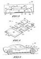
- FIG. 5is a side view of an automobile implementing a packaged electronic device according to the present invention.
- FIG. 6is a block diagram of a video game device implementing a packaged electronic device according to the present invention.
- FIG. 2shows a top view of a lead frame for a packaged electronic device according to the present invention.
- Lead frame 201includes a die mounting location 203 located on its top side (relative to the view shown in FIG. 2 ).
- Die mounting location 203defines the location of a die with respect to a lead frame in a packaged electronic device.
- Lead frame 201includes four split flag structures 205 , 207 , 209 , and 211 .
- the top side of each flag structureincludes a portion of die mounting location 203 .
- lead frame 201also includes wire bond pads (e.g. 220 ) where wires (not shown) are bonded for coupling to the bond pads (not shown) of the die via bond wires (e.g. 315 of FIG. 3 ). After encapsulating lead frame 201 and die, portions (e.g. 222 ) of lead frame 201 are trimmed.
- wire bond padse.g. 220
- bond wirese.g. 315 of FIG. 3
- the bottom sides (relative to the view shown in FIG. 2 ) of the wire bond pads (e.g. 220 )are exposed from encapsulation to serve as bond pads for external coupling of the die to e.g. a printed circuit board.
- other types of external conductive structurese.g. balls or bumps may be coupled to the wirebond pads of the lead frame for external coupling of the die.
- Lead frame 201includes support structures 219 , 221 , 223 , and 225 located between flag structures 205 , 207 , 209 , and 211 .
- Support structures 219 , 221 , 223 , and 225provide support for the flag structures prior to the encapsulation.
- Each support structuree.g. 219
- Each support structureincludes at least one bend portion (e.g. 233 ) for providing stress relief between the two flag structures (e.g. 205 and 207 ) and die.
- the bend portions of the support structuresallow for the flag structures to move laterally with respect to each other to reduce stress of the package during manufacture as well as during the operation of the device.
- the lateral movementincludes lateral movement of the flag structures in a direction extending between the flag structures.
- lead frame 201may include a lesser number or greater number of split flag structures with support structures located there between.
- the support structureseach have an “S” form with the portions of the support structure connected at 90 degree angles with each other.
- portion 231is connected to portion 235 at a 90 degree angle.
- Portion 237is connected to portion 235 at a 90 degree angle.
- Portion 231is connected to flag structure 205 and portion 237 is connected to flag structure 207 .
- the support structuresmay have other forms such as forms having rounded corners. With some embodiments, the support structures may have a zig zag form. With some of these forms, portions of the support structure may extend from the flag structures at non 90 degree angles.
- Lead frame 201is formed from a sheet (not shown) of suitable lead frame material (e.g. copper) using any one of a number of forming processes.
- the sheet of lead frame materialis stamped and/or chemically etched with a pattern that includes patterns for multiple lead frames (e.g. 201 ).
- the lead frame patternsare arranged in columns and rows in the sheet.
- FIG. 3is a side view of an embodiment of a packaged electronic device according to the present invention.
- Packaged electronic device 301includes a bottom die 305 and a top die 303 located in a stacked die configuration with a spacer 307 located there between. Some embodiments do not include spacer 307 .
- Die 305is mounted to lead frame 309 at a die mounting location of lead frame 309 .
- packaged electronic device 301is a packaged sensor device with a transducer being implemented in one of die 303 and die 305 and a signal controller application specific integrated circuit (ASIC) being implemented in the other of die 303 and die 305 for converting the mechanical signal into an electrical signal.
- ASICapplication specific integrated circuit
- the transducer and signal controllermaybe implemented in the same die.
- Lead frame 309is similar to lead frame 201 in that it includes four split flag structures with flag structures 328 and 329 shown in FIG. 3 . Lead frame 309 also includes four support structures coupled between the split flag structures with support structure 327 shown in FIG. 3 coupling flag structures 328 and 329 together.
- the support structures (e.g. 327 ) of lead frame 309include bend portions for providing stress relief.
- Lead frame 309includes wire bond pads (e.g. 311 and 312 ). Bond wires (e.g. 325 ) are bonded to bond pads (e.g. 321 ) of die 305 and to the wire bond pads of lead frame 309 .
- Packaged electronic device 301also include bond wires (e.g. 323 ) that couple the bond pads of die 303 (e.g. 331 ) to the bond pads (e.g. 321 ) of die 305 .
- FIG. 3shows only two die bond pads for die 303 and die 305 , die in other embodiments may include more.
- die 303includes a mechanical sensing structure (MEMS) and die 305 includes a signal conditioning controller.
- packaged electronic device 301is configured in a Quad Flat No-Leads (QFN) configuration.
- QFNQuad Flat No-Leads
- a lead frame having a support structure coupling flag structuresmay be implemented in packaged electronic devices of other types of package configurations such as e.g. plastic dual in-line package (PDIP), small outline integrated circuit (SOIC), and ball grid array (BGA), etc.
- PDIPplastic dual in-line package
- SOICsmall outline integrated circuit
- BGAball grid array
- lead frame 309is formed from a sheet of lead frame material (not shown).
- the sheetis a 8′′ ⁇ 2.5′′ copper plate having a thickness of between 5 to 15 mils, but may have other dimensions in other embodiments.
- the sheetis stamped to define multiple lead frames in rows and columns.
- the sheet of lead frame materialmay be patterned by etching.
- the support structuresare etched from both the top and bottom of the sheet of lead frame material to reduce the thickness of the support structures.
- the support structurese.g. 327
- the support structuresare about half the width of the split flag structures (e.g. 328 and 329 ). Reducing the thickness of the support structures (e.g. 327 ) allows the support structure to be encapsulated without the bottom of the support structure being exposed from encapsulation.
- the dieare attached to the lead frames at the die mounting locations.
- the dieare attached to the lead frames with conductive epoxy.
- the dieare attached by attaching the die to pads or spacers attached to the lead frame at the pad mounting locations.
- the bond pads (e.g. 321 ) of the diee.g. 305
- the bond pads (e.g. 312 ) of the lead framesare wire bonded to the bond pads (e.g. 312 ) of the lead frames.
- spacerse.g. 307
- top sides of the bottom diee.g. 305
- Top diee.g.
- the bond pads (e.g. 331 ) of the top die (e.g. 303 )are wire bonded to bond pads (e.g. 321 ) of the bottom die.
- the resultant sheet and attached dieare then encapsulated in an encapsulant (e.g. 317 ).
- the encapsulated structureis then cut to singulate the packaged electronic devices.
- the packaged electronic devicesare then tested and shipped.
- Packaged electronic devices of other configurationsmay be manufactured by other processes.
- a lead frame having flag structures coupled by a support structure having at least one bend portionprovides stress relief for a lead frame of a packaged electronic device during its manufacture and during operation.
- the use of support structures to couple split flag structuresmay reduce or eliminate the need for a gel (e.g. 109 ) or rubber pads (e.g. 113 ) in the packaged electronic device. Accordingly, problems associated with different temperature coefficients between the gel and encapsulant (e.g. gaps) may be eliminated or significantly reduced as well as the cost and complexity of the manufacture of the packaged electronic device may be reduced as well.
- Another advantage of adopting such a lead frame design in a QFN configurationis that it may result in a package with a significantly smaller footprint. Providing a support structure coupling these flag structures and having at least a portion of the support structure between two flag structures may reduce stress during encapsulation and provides support between the two flag structures during manufacture.
- FIG. 4is a perspective view of another lead frame according to the present invention.
- Lead frame 401includes two die mounting locations 405 and 403 .
- Die mounting location 403is located at a first side of four split flag structures 421 , 423 , 425 , and 427 .
- Die mounting location 405is located at a first side of flag structure 404 .
- Flag structures 421 and 423are coupled via a support structure 411 which has two bend portions, and flag structures 425 and 427 are coupled via support structure 409 .
- flag structure 423is coupled to flag structure 404 via a support structure 413 having a bend portion
- flag structure 427is coupled to flag structure 404 via support structure 417 .
- a die including a transduceris located at die mounting location 403 and a die including a signal controller operably coupled to the transducer of the die is located at die mounting location 405 .
- a packaged sensor device configurationcan be used to implement an inertial sensor.
- the signal controllerwould be operably coupled to other circuitry (not shown) external to the packaged electronic device.
- such a packaged sensor device configurationmaybe used to implement other types of sensors.
- FIG. 5is a side view of one embodiment of a car according to the present invention.
- Car 501includes a number of packaged electronic devices (e.g. 515 , 505 , 512 , 511 , 510 , and 519 ) that include a lead frame with two flag structures coupled with a structure having a bend portion.
- These packaged electronic devicesimplement accelerometers or other types of inertial sensors such as e.g. angular sensors for measuring angular velocity or acceleration.
- Packaged electronic devices 515 , 519 , and 512provide acceleration sensing for air bag deployment.
- Packaged electronic device 505provides central crash sensing. Other packaged electronic devices can be utilized for providing rollover detection.
- Packaged electronic device 511is utilized to provide braking detection.
- Car 501may include other packaged electronic devices for providing other sensed information including side impact detection. These packaged electronic devices each include an inertial sensor. Each of the packaged electronic devices is operably coupled to a central controller (e.g. by a wired coupling or wireless coupling) for providing the information sensed by the sensing circuitry of the packaged electronic device to the central controller for operation. Packaged electronic devices as shown and described above may be implemented in other types of automobiles such as e.g. trucks, pickups, SUVs, motorcycles, and vans.
- FIG. 6is a block diagram of one embodiment a video game device according to the present invention.
- Video game device 601includes a screen 603 , control unit 604 , and hand held peripheral unit 605 which is operably coupled to control unit 605 via e.g. a wired coupling or wireless coupling. Some video game devices do not include a screen, wherein control unit 605 is operably couplable to a television to provide image information for display.
- Peripheral unit 605includes an inertial sensor 606 implemented in a packaged electronic device having a lead frame similar to lead frame 401 or lead frame 201 .
- the screen 603 , control unit 604 , and peripheral unit 605are implemented in one housing.
- Packaged electronic devices having lead frames similar to those described abovemay be implemented in other types of devices such as airplanes, cell phones, appliances, space craft and other space devices, or other devices requiring inertia and/or gyration detection. Furthermore, lead frames similar to those described above may be included in packaged electronic devices with die implementing other types of circuitry such as e.g. micro controllers, digital signal processors, logic circuitry, and memories.
- circuitrye.g. micro controllers, digital signal processors, logic circuitry, and memories.
Landscapes
- Physics & Mathematics (AREA)
- Engineering & Computer Science (AREA)
- Computer Hardware Design (AREA)
- Microelectronics & Electronic Packaging (AREA)
- Power Engineering (AREA)
- Condensed Matter Physics & Semiconductors (AREA)
- General Physics & Mathematics (AREA)
- Geometry (AREA)
- Lead Frames For Integrated Circuits (AREA)
- Gyroscopes (AREA)
- Micromachines (AREA)
- Pressure Sensors (AREA)
Abstract
Description
- 1. Field of the Invention
- This invention relates in general to packaged electronic devices and specifically to lead frames for packaged electronic devices.
- 2. Description of the Related Art
- Electrical circuits such as integrated circuits can be implemented in packaged electronic devices. A packaged electronic device may include one or more lead frames and one or more die for implementing electrical circuits of the packaged electronic device. In some embodiments, the die and lead frame(s) may be encapsulated with an encapsulant.
- Because the packaging of die includes different materials (e.g. metal, encapsulant), temperature variations may cause the packaged die to be stressed during manufacture and operating conditions due to the differences in thermal expansion and other material properties of the different materials. For some packaged electronic devices that include some types of circuits and transducers (e.g. a sensor), this stress may affect the operation of the device.
FIG. 1 is a partial cross sectional view of a prior art packaged electronic device. Packagedelectronic device 101 includes afirst die 105 and a second die107 attached to the top of die105. Die105 and die107 are utilized to implement a sensor. Located between die105 andlead frame 103 are four rubber or adhesive pads (with rubber oradhesive pads FIG. 1 ). The rubber pads isolate die105 from stress alonglead frame 103. The rubber or adhesive pads are attached to a flag structure oflead frame 103. Prior to encapsulation, die105, die107 and the rubber pads are enclosed in agel 109 for further stress isolation. This stress isolation may be done for the sensor to function electrically within accepted specifications in the operating temperature range. After wire bonding, the entire assembly is encapsulated withencapsulant 115 at an elevated temperature. After cooling back to room temperature, an air gap (not shown) is formed between the gel and encapsulant due to a much faster shrinkage of the gel compared to the encapsulant. The air gap shields die105 and die107 from the packaging stress caused byencapsulant 115 andlead frame 103.- Such a stress isolation process is complicated and the process control is often difficult. In addition, to accommodate the inclusion of the gel, the resulting package that is simpler, smaller, and with significantly reduced packaging stress to an electronic device.
- The present invention may be better understood, and its numerous objects, features, and advantages made apparent to those skilled in the art by referencing the accompanying drawings.
FIG. 1 is a partial cross sectional view of a prior art packaged electronic device.FIG. 2 is a top view of one embodiment of a lead frame for a packaged electronic device according to the present invention.FIG. 3 is cut away side view of one embodiment of a packaged electronic device according to the present invention.FIG. 4 is a perspective view of another embodiment of a lead frame according to the present invention.FIG. 5 is a side view of an automobile implementing a packaged electronic device according to the present invention.FIG. 6 is a block diagram of a video game device implementing a packaged electronic device according to the present invention.- The use of the same reference symbols in different drawings indicates identical items unless otherwise noted.
- The following sets forth a detailed description of a mode for carrying out the invention. The description is intended to be illustrative of the invention and should not be taken to be limiting.
FIG. 2 shows a top view of a lead frame for a packaged electronic device according to the present invention.Lead frame 201 includes adie mounting location 203 located on its top side (relative to the view shown inFIG. 2 ). Diemounting location 203 defines the location of a die with respect to a lead frame in a packaged electronic device.Lead frame 201 includes foursplit flag structures die mounting location 203.- In the embodiment shown,
lead frame 201 also includes wire bond pads (e.g.220) where wires (not shown) are bonded for coupling to the bond pads (not shown) of the die via bond wires (e.g.315 ofFIG. 3 ). After encapsulatinglead frame 201 and die, portions (e.g.222) oflead frame 201 are trimmed. - In other embodiments, the bottom sides (relative to the view shown in
FIG. 2 ) of the wire bond pads (e.g.220) are exposed from encapsulation to serve as bond pads for external coupling of the die to e.g. a printed circuit board. With other embodiments, other types of external conductive structures (e.g. balls or bumps) may be coupled to the wirebond pads of the lead frame for external coupling of the die. Lead frame 201 includessupport structures flag structures Support structures lead frame 201 may include a lesser number or greater number of split flag structures with support structures located there between.- In the embodiment shown, the support structures (e.g.219) each have an “S” form with the portions of the support structure connected at 90 degree angles with each other. For example,
portion 231 is connected toportion 235 at a 90 degree angle.Portion 237 is connected toportion 235 at a 90 degree angle.Portion 231 is connected toflag structure 205 andportion 237 is connected toflag structure 207. - In other embodiments, the support structures may have other forms such as forms having rounded corners. With some embodiments, the support structures may have a zig zag form. With some of these forms, portions of the support structure may extend from the flag structures at non 90 degree angles.
Lead frame 201 is formed from a sheet (not shown) of suitable lead frame material (e.g. copper) using any one of a number of forming processes. In forming one embodiment of a lead frame, the sheet of lead frame material is stamped and/or chemically etched with a pattern that includes patterns for multiple lead frames (e.g.201). In some embodiments, the lead frame patterns are arranged in columns and rows in the sheet.FIG. 3 is a side view of an embodiment of a packaged electronic device according to the present invention. Packagedelectronic device 301 includes a bottom die305 and a top die303 located in a stacked die configuration with aspacer 307 located there between. Some embodiments do not includespacer 307. Die305 is mounted tolead frame 309 at a die mounting location oflead frame 309. In one embodiment, packagedelectronic device 301 is a packaged sensor device with a transducer being implemented in one ofdie 303 and die305 and a signal controller application specific integrated circuit (ASIC) being implemented in the other ofdie 303 and die305 for converting the mechanical signal into an electrical signal. In some embodiments, the transducer and signal controller maybe implemented in the same die.Lead frame 309 is similar to leadframe 201 in that it includes four split flag structures withflag structures FIG. 3 .Lead frame 309 also includes four support structures coupled between the split flag structures withsupport structure 327 shown inFIG. 3 coupling flag structures lead frame 309 include bend portions for providing stress relief.Lead frame 309 includes wire bond pads (e.g.311 and312). Bond wires (e.g.325) are bonded to bond pads (e.g.321) ofdie 305 and to the wire bond pads oflead frame 309. Packagedelectronic device 301 also include bond wires (e.g.323) that couple the bond pads of die303 (e.g.331) to the bond pads (e.g.321) ofdie 305. Although,FIG. 3 shows only two die bond pads fordie 303 and die305, die in other embodiments may include more.- In one embodiment, die303 includes a mechanical sensing structure (MEMS) and die305 includes a signal conditioning controller. In one embodiment, packaged
electronic device 301 is configured in a Quad Flat No-Leads (QFN) configuration. However a lead frame having a support structure coupling flag structures may be implemented in packaged electronic devices of other types of package configurations such as e.g. plastic dual in-line package (PDIP), small outline integrated circuit (SOIC), and ball grid array (BGA), etc. - In one embodiment,
lead frame 309 is formed from a sheet of lead frame material (not shown). In one embodiment, the sheet is a 8″×2.5″ copper plate having a thickness of between 5 to 15 mils, but may have other dimensions in other embodiments. The sheet is stamped to define multiple lead frames in rows and columns. In other embodiments, the sheet of lead frame material may be patterned by etching. After the lead frames in the sheet have been defined, the support structures are etched from both the top and bottom of the sheet of lead frame material to reduce the thickness of the support structures. In the embodiment ofFIG. 3 , the support structures (e.g.327) are about half the width of the split flag structures (e.g.328 and329). Reducing the thickness of the support structures (e.g.327) allows the support structure to be encapsulated without the bottom of the support structure being exposed from encapsulation. - After the lead frames have been formed in the sheet of lead frame material, the die are attached to the lead frames at the die mounting locations. In one embodiment, the die are attached to the lead frames with conductive epoxy. In other embodiments, the die are attached by attaching the die to pads or spacers attached to the lead frame at the pad mounting locations. Afterwards, the bond pads (e.g.321) of the die (e.g.305) are wire bonded to the bond pads (e.g.312) of the lead frames.
- With some packaged electronic devices having a stacked die configuration, spacers (e.g.307) are then attached to the top sides of the bottom die (e.g.305). Top die (e.g.
- 303) are attached to the opposite sides of the spacers. The bond pads (e.g.331) of the top die (e.g.303) are wire bonded to bond pads (e.g.321) of the bottom die. The resultant sheet and attached die are then encapsulated in an encapsulant (e.g.317). The encapsulated structure is then cut to singulate the packaged electronic devices. The packaged electronic devices are then tested and shipped. Packaged electronic devices of other configurations may be manufactured by other processes.
- One advantage that may occur with a lead frame having flag structures coupled by a support structure having at least one bend portion is that it provides stress relief for a lead frame of a packaged electronic device during its manufacture and during operation. With some embodiments, the use of support structures to couple split flag structures may reduce or eliminate the need for a gel (e.g.109) or rubber pads (e.g.113) in the packaged electronic device. Accordingly, problems associated with different temperature coefficients between the gel and encapsulant (e.g. gaps) may be eliminated or significantly reduced as well as the cost and complexity of the manufacture of the packaged electronic device may be reduced as well. Another advantage of adopting such a lead frame design in a QFN configuration is that it may result in a package with a significantly smaller footprint. Providing a support structure coupling these flag structures and having at least a portion of the support structure between two flag structures may reduce stress during encapsulation and provides support between the two flag structures during manufacture.
FIG. 4 is a perspective view of another lead frame according to the present invention.Lead frame 401 includes twodie mounting locations location 403 is located at a first side of foursplit flag structures location 405 is located at a first side offlag structure 404.Flag structures support structure 411 which has two bend portions, andflag structures support structure 409. In the embodiment shown,flag structure 423 is coupled toflag structure 404 via asupport structure 413 having a bend portion, andflag structure 427 is coupled toflag structure 404 viasupport structure 417.- In one embodiment of a packaged sensor device including
lead frame 401, a die including a transducer is located atdie mounting location 403 and a die including a signal controller operably coupled to the transducer of the die is located atdie mounting location 405. Such a packaged sensor device configuration can be used to implement an inertial sensor. In some embodiments, the signal controller would be operably coupled to other circuitry (not shown) external to the packaged electronic device. With other embodiments, such a packaged sensor device configuration maybe used to implement other types of sensors. FIG. 5 is a side view of one embodiment of a car according to the present invention.Car 501 includes a number of packaged electronic devices (e.g.515,505,512,511,510, and519) that include a lead frame with two flag structures coupled with a structure having a bend portion. These packaged electronic devices implement accelerometers or other types of inertial sensors such as e.g. angular sensors for measuring angular velocity or acceleration. Packagedelectronic devices electronic device 505 provides central crash sensing. Other packaged electronic devices can be utilized for providing rollover detection. Packagedelectronic device 511 is utilized to provide braking detection.Car 501 may include other packaged electronic devices for providing other sensed information including side impact detection. These packaged electronic devices each include an inertial sensor. Each of the packaged electronic devices is operably coupled to a central controller (e.g. by a wired coupling or wireless coupling) for providing the information sensed by the sensing circuitry of the packaged electronic device to the central controller for operation. Packaged electronic devices as shown and described above may be implemented in other types of automobiles such as e.g. trucks, pickups, SUVs, motorcycles, and vans.FIG. 6 is a block diagram of one embodiment a video game device according to the present invention.Video game device 601 includes ascreen 603,control unit 604, and hand heldperipheral unit 605 which is operably coupled to controlunit 605 via e.g. a wired coupling or wireless coupling. Some video game devices do not include a screen, whereincontrol unit 605 is operably couplable to a television to provide image information for display.Peripheral unit 605 includes aninertial sensor 606 implemented in a packaged electronic device having a lead frame similar to leadframe 401 orlead frame 201. In some embodiments, thescreen 603,control unit 604, andperipheral unit 605 are implemented in one housing.- Packaged electronic devices having lead frames similar to those described above may be implemented in other types of devices such as airplanes, cell phones, appliances, space craft and other space devices, or other devices requiring inertia and/or gyration detection. Furthermore, lead frames similar to those described above may be included in packaged electronic devices with die implementing other types of circuitry such as e.g. micro controllers, digital signal processors, logic circuitry, and memories.
- While particular embodiments of the present invention have been shown and described, it will be recognized to those skilled in the art that, based upon the teachings herein, further changes and modifications may be made without departing from this invention and its broader aspects, and thus, the appended claims are to encompass within their scope all such changes and modifications as are within the true spirit and scope of this invention.
Claims (34)
Priority Applications (3)
| Application Number | Priority Date | Filing Date | Title |
|---|---|---|---|
| US10/660,828US7012324B2 (en) | 2003-09-12 | 2003-09-12 | Lead frame with flag support structure |
| PCT/US2004/027934WO2005034177A2 (en) | 2003-09-12 | 2004-08-27 | Lead frame with flag support structure |
| TW093127204ATW200518305A (en) | 2003-09-12 | 2004-09-08 | Lead frame with flag support structure |
Applications Claiming Priority (1)
| Application Number | Priority Date | Filing Date | Title |
|---|---|---|---|
| US10/660,828US7012324B2 (en) | 2003-09-12 | 2003-09-12 | Lead frame with flag support structure |
Publications (2)
| Publication Number | Publication Date |
|---|---|
| US20050056920A1true US20050056920A1 (en) | 2005-03-17 |
| US7012324B2 US7012324B2 (en) | 2006-03-14 |
Family
ID=34273727
Family Applications (1)
| Application Number | Title | Priority Date | Filing Date |
|---|---|---|---|
| US10/660,828Expired - Fee RelatedUS7012324B2 (en) | 2003-09-12 | 2003-09-12 | Lead frame with flag support structure |
Country Status (3)
| Country | Link |
|---|---|
| US (1) | US7012324B2 (en) |
| TW (1) | TW200518305A (en) |
| WO (1) | WO2005034177A2 (en) |
Cited By (8)
| Publication number | Priority date | Publication date | Assignee | Title |
|---|---|---|---|---|
| US20060002666A1 (en)* | 2004-06-30 | 2006-01-05 | Ice Donald A | Shaped lead assembly for optoelectronic devices |
| US20060220189A1 (en)* | 2005-03-30 | 2006-10-05 | Noriaki Sakamoto | Semiconductor module and method of manufacturing the same |
| US20070152314A1 (en)* | 2005-12-30 | 2007-07-05 | Intel Corporation | Low stress stacked die packages |
| US20080186680A1 (en)* | 2004-04-24 | 2008-08-07 | Achim Henkel | Monolithic Controller for the Generator Unit of a Motor Vehicle |
| US20090146278A1 (en)* | 2006-09-12 | 2009-06-11 | Chipmos Technologies Inc. | Chip-stacked package structure with asymmetrical leadframe |
| US8436460B1 (en)* | 2007-05-04 | 2013-05-07 | Cypress Semiconductor Corporation | Multiple die paddle leadframe and semiconductor device package |
| WO2014020034A1 (en)* | 2012-07-30 | 2014-02-06 | Continental Teves Ag & Co. Ohg | Wiring device for wiring an electronic apparatus |
| US11185306B2 (en)* | 2018-01-31 | 2021-11-30 | Samsung Medison Co., Ltd. | Ultrasound probe |
Families Citing this family (10)
| Publication number | Priority date | Publication date | Assignee | Title |
|---|---|---|---|---|
| US7303949B2 (en)* | 2003-10-20 | 2007-12-04 | International Business Machines Corporation | High performance stress-enhanced MOSFETs using Si:C and SiGe epitaxial source/drain and method of manufacture |
| DE10350239A1 (en)* | 2003-10-27 | 2005-06-16 | Infineon Technologies Ag | Semiconductor component with housing plastic material, semiconductor chip and circuit carrier and method for producing the same |
| JP4878580B2 (en)* | 2007-05-30 | 2012-02-15 | ルネサスエレクトロニクス株式会社 | Lead frame and manufacturing method thereof, semiconductor device and manufacturing method thereof |
| US7759806B2 (en)* | 2007-09-20 | 2010-07-20 | Stats Chippac Ltd. | Integrated circuit package system with multiple device units |
| US20110193207A1 (en)* | 2010-02-09 | 2011-08-11 | Freescale Semiconductor, Inc | Lead frame for semiconductor die |
| US20110227173A1 (en)* | 2010-03-17 | 2011-09-22 | Honeywell International Inc. | Mems sensor with integrated asic packaging |
| US9034697B2 (en)* | 2011-07-14 | 2015-05-19 | Freescale Semiconductor, Inc. | Apparatus and methods for quad flat no lead packaging |
| JP5954013B2 (en)* | 2012-07-18 | 2016-07-20 | 日亜化学工業株式会社 | Semiconductor element mounting member and semiconductor device |
| CN202839587U (en) | 2012-07-27 | 2013-03-27 | 飞思卡尔半导体公司 | Surface mounting semiconductor device |
| CN104867838B (en) | 2014-02-25 | 2019-01-08 | 恩智浦美国有限公司 | Semiconductor die package with pre-molded tube core |
Citations (7)
| Publication number | Priority date | Publication date | Assignee | Title |
|---|---|---|---|---|
| US4924291A (en)* | 1988-10-24 | 1990-05-08 | Motorola Inc. | Flagless semiconductor package |
| US5019893A (en)* | 1990-03-01 | 1991-05-28 | Motorola, Inc. | Single package, multiple, electrically isolated power semiconductor devices |
| US5327008A (en)* | 1993-03-22 | 1994-07-05 | Motorola Inc. | Semiconductor device having universal low-stress die support and method for making the same |
| US5381036A (en)* | 1992-02-03 | 1995-01-10 | Motorola, Inc. | Lead-on chip semiconductor device having peripheral bond pads |
| US5683944A (en)* | 1995-09-01 | 1997-11-04 | Motorola, Inc. | Method of fabricating a thermally enhanced lead frame |
| US6081029A (en)* | 1998-03-12 | 2000-06-27 | Matsushita Electronics Corporation | Resin encapsulated semiconductor device having a reduced thickness and improved reliability |
| US6399423B2 (en)* | 1999-12-27 | 2002-06-04 | Hitachi, Ltd | Semiconductor device an a method of manufacturing the same |
Family Cites Families (22)
| Publication number | Priority date | Publication date | Assignee | Title |
|---|---|---|---|---|
| JPS559401A (en) | 1978-07-05 | 1980-01-23 | Hitachi Ltd | Leed frame |
| US4829362A (en) | 1986-04-28 | 1989-05-09 | Motorola, Inc. | Lead frame with die bond flag for ceramic packages |
| JPH0350758A (en) | 1989-07-18 | 1991-03-05 | Toshiba Corp | Resin-encapsulated semiconductor device |
| US5068764A (en) | 1990-03-05 | 1991-11-26 | Thermalloy Incorporated | Electronic device package mounting assembly |
| EP0452634B1 (en) | 1990-03-16 | 1997-05-02 | Sumitomo Electric Industries, Ltd. | Lead frame for semiconductor device |
| US5049973A (en) | 1990-06-26 | 1991-09-17 | Harris Semiconductor Patents, Inc. | Heat sink and multi mount pad lead frame package and method for electrically isolating semiconductor die(s) |
| US5233222A (en) | 1992-07-27 | 1993-08-03 | Motorola, Inc. | Semiconductor device having window-frame flag with tapered edge in opening |
| US5565749A (en) | 1993-04-28 | 1996-10-15 | Kabushiki Kaisha Toshiba | Method of controlling a grinder robot |
| US5767443A (en) | 1993-07-10 | 1998-06-16 | Micron Technology, Inc. | Multi-die encapsulation device |
| US5594234A (en) | 1994-11-14 | 1997-01-14 | Texas Instruments Incorporated | Downset exposed die mount pad leadframe and package |
| JPH0964266A (en) | 1995-08-18 | 1997-03-07 | Sony Corp | Lead frame |
| SG46955A1 (en) | 1995-10-28 | 1998-03-20 | Inst Of Microelectronics | Ic packaging lead frame for reducing chip stress and deformation |
| US5739586A (en) | 1996-08-30 | 1998-04-14 | Scientific-Atlanta, Inc. | Heat sink assembly including a printed wiring board and a metal case |
| US5856911A (en) | 1996-11-12 | 1999-01-05 | National Semiconductor Corporation | Attachment assembly for integrated circuits |
| JPH10321791A (en) | 1997-03-17 | 1998-12-04 | Tokai Rika Co Ltd | Operational amplifier |
| EP0887850A3 (en) | 1997-06-23 | 2001-05-02 | STMicroelectronics, Inc. | Lead-frame forming for improved thermal performance |
| US6049125A (en) | 1997-12-29 | 2000-04-11 | Micron Technology, Inc. | Semiconductor package with heat sink and method of fabrication |
| US5969949A (en) | 1998-03-31 | 1999-10-19 | Sun Microsystems, Inc. | Interfitting heat sink and heat spreader slug |
| US5969950A (en) | 1998-11-04 | 1999-10-19 | Sun Microsystems, Inc. | Enhanced heat sink attachment |
| US6163068A (en) | 1999-04-22 | 2000-12-19 | Yao; Hsia Kuang | Multi-chip semiconductor encapsulation method and its finished product |
| DE10106838C2 (en)* | 2001-02-14 | 2003-04-30 | Infineon Technologies Ag | Sensor device for capturing biometric features, especially finger minutiae |
| US6996897B2 (en) | 2002-07-31 | 2006-02-14 | Freescale Semiconductor, Inc. | Method of making a mount for electronic devices |
- 2003
- 2003-09-12USUS10/660,828patent/US7012324B2/ennot_activeExpired - Fee Related
- 2004
- 2004-08-27WOPCT/US2004/027934patent/WO2005034177A2/enactiveApplication Filing
- 2004-09-08TWTW093127204Apatent/TW200518305A/enunknown
Patent Citations (8)
| Publication number | Priority date | Publication date | Assignee | Title |
|---|---|---|---|---|
| US4924291A (en)* | 1988-10-24 | 1990-05-08 | Motorola Inc. | Flagless semiconductor package |
| US5019893A (en)* | 1990-03-01 | 1991-05-28 | Motorola, Inc. | Single package, multiple, electrically isolated power semiconductor devices |
| US5381036A (en)* | 1992-02-03 | 1995-01-10 | Motorola, Inc. | Lead-on chip semiconductor device having peripheral bond pads |
| US5327008A (en)* | 1993-03-22 | 1994-07-05 | Motorola Inc. | Semiconductor device having universal low-stress die support and method for making the same |
| US5424576A (en)* | 1993-03-22 | 1995-06-13 | Motorola, Inc. | Semiconductor device having x-shaped die support member and method for making the same |
| US5683944A (en)* | 1995-09-01 | 1997-11-04 | Motorola, Inc. | Method of fabricating a thermally enhanced lead frame |
| US6081029A (en)* | 1998-03-12 | 2000-06-27 | Matsushita Electronics Corporation | Resin encapsulated semiconductor device having a reduced thickness and improved reliability |
| US6399423B2 (en)* | 1999-12-27 | 2002-06-04 | Hitachi, Ltd | Semiconductor device an a method of manufacturing the same |
Cited By (10)
| Publication number | Priority date | Publication date | Assignee | Title |
|---|---|---|---|---|
| US20080186680A1 (en)* | 2004-04-24 | 2008-08-07 | Achim Henkel | Monolithic Controller for the Generator Unit of a Motor Vehicle |
| US20060002666A1 (en)* | 2004-06-30 | 2006-01-05 | Ice Donald A | Shaped lead assembly for optoelectronic devices |
| US20060220189A1 (en)* | 2005-03-30 | 2006-10-05 | Noriaki Sakamoto | Semiconductor module and method of manufacturing the same |
| US7332808B2 (en)* | 2005-03-30 | 2008-02-19 | Sanyo Electric Co., Ltd. | Semiconductor module and method of manufacturing the same |
| US20070152314A1 (en)* | 2005-12-30 | 2007-07-05 | Intel Corporation | Low stress stacked die packages |
| US20090146278A1 (en)* | 2006-09-12 | 2009-06-11 | Chipmos Technologies Inc. | Chip-stacked package structure with asymmetrical leadframe |
| US8436460B1 (en)* | 2007-05-04 | 2013-05-07 | Cypress Semiconductor Corporation | Multiple die paddle leadframe and semiconductor device package |
| WO2014020034A1 (en)* | 2012-07-30 | 2014-02-06 | Continental Teves Ag & Co. Ohg | Wiring device for wiring an electronic apparatus |
| US9661775B2 (en) | 2012-07-30 | 2017-05-23 | Continental Teves Ag & Co. Ohg | Wiring device for wiring an electronic apparatus |
| US11185306B2 (en)* | 2018-01-31 | 2021-11-30 | Samsung Medison Co., Ltd. | Ultrasound probe |
Also Published As
| Publication number | Publication date |
|---|---|
| WO2005034177A2 (en) | 2005-04-14 |
| TW200518305A (en) | 2005-06-01 |
| US7012324B2 (en) | 2006-03-14 |
| WO2005034177A3 (en) | 2006-03-30 |
Similar Documents
| Publication | Publication Date | Title |
|---|---|---|
| US7012324B2 (en) | Lead frame with flag support structure | |
| US6035712A (en) | Sensor device and method of producing the same using lead frame | |
| US9656856B2 (en) | Method of lower profile MEMS package with stress isolations | |
| US7370530B2 (en) | Package for MEMS devices | |
| US9475694B2 (en) | Two-axis vertical mount package assembly | |
| EP2434297A1 (en) | Structure having chip mounted thereon and module provided with the structure | |
| US20110156176A1 (en) | Leadframe-Based Premolded Package Having Acoustic Air Channel for Micro-Electro-Mechanical System | |
| US20090282917A1 (en) | Integrated multi-axis micromachined inertial sensing unit and method of fabrication | |
| CN108574472B (en) | Vibrating devices, oscillators, electronic equipment and moving objects | |
| WO2014208116A1 (en) | Transfer-molding-type sensor device | |
| US7836764B2 (en) | Electrical device with covering | |
| US6323529B1 (en) | Semiconductor acceleration sensor and a method of manufacturing the same | |
| US20150355220A1 (en) | Inertial sensor module having hermetic seal formed of metal and multi-axis sensor employing the same | |
| US20070277607A1 (en) | Semiconductor acceleration sensor | |
| JP2005127750A (en) | Semiconductor sensor and its manufacturing method | |
| JP4428210B2 (en) | Mounting structure of physical quantity sensor | |
| JPWO2007020701A1 (en) | Acceleration sensor device | |
| CN105189337B (en) | Microelectromechanical device and manufacturing method | |
| JP2765610B2 (en) | Semiconductor vibration / acceleration detector | |
| JP4706634B2 (en) | Semiconductor sensor and manufacturing method thereof | |
| JP4566066B2 (en) | Circuit device and manufacturing method thereof | |
| JP7512785B2 (en) | Electronics | |
| JP2011142229A (en) | Package for electronic component, electronic component device, and method of manufacturing electronic component device | |
| JPH0727785A (en) | Acceleration sensor | |
| JP2007007774A (en) | Package for micro electro mechanical device and manufacturing method thereof |
Legal Events
| Date | Code | Title | Description |
|---|---|---|---|
| AS | Assignment | Owner name:MOTOROLA, INC., ILLINOIS Free format text:ASSIGNMENT OF ASSIGNORS INTEREST;ASSIGNORS:LI, GARY G.;CHAPMAN, MICHAEL E. S.;MAHADEVAN, DAVE S.;REEL/FRAME:014500/0785 Effective date:20030904 | |
| AS | Assignment | Owner name:FREESCALE SEMICONDUCTOR, INC., TEXAS Free format text:ASSIGNMENT OF ASSIGNORS INTEREST;ASSIGNOR:MOTOROLA, INC;REEL/FRAME:015360/0718 Effective date:20040404 Owner name:FREESCALE SEMICONDUCTOR, INC.,TEXAS Free format text:ASSIGNMENT OF ASSIGNORS INTEREST;ASSIGNOR:MOTOROLA, INC;REEL/FRAME:015360/0718 Effective date:20040404 | |
| AS | Assignment | Owner name:CITIBANK, N.A. AS COLLATERAL AGENT, NEW YORK Free format text:SECURITY AGREEMENT;ASSIGNORS:FREESCALE SEMICONDUCTOR, INC.;FREESCALE ACQUISITION CORPORATION;FREESCALE ACQUISITION HOLDINGS CORP.;AND OTHERS;REEL/FRAME:018855/0129 Effective date:20061201 Owner name:CITIBANK, N.A. AS COLLATERAL AGENT,NEW YORK Free format text:SECURITY AGREEMENT;ASSIGNORS:FREESCALE SEMICONDUCTOR, INC.;FREESCALE ACQUISITION CORPORATION;FREESCALE ACQUISITION HOLDINGS CORP.;AND OTHERS;REEL/FRAME:018855/0129 Effective date:20061201 | |
| FPAY | Fee payment | Year of fee payment:4 | |
| AS | Assignment | Owner name:CITIBANK, N.A., AS COLLATERAL AGENT,NEW YORK Free format text:SECURITY AGREEMENT;ASSIGNOR:FREESCALE SEMICONDUCTOR, INC.;REEL/FRAME:024397/0001 Effective date:20100413 Owner name:CITIBANK, N.A., AS COLLATERAL AGENT, NEW YORK Free format text:SECURITY AGREEMENT;ASSIGNOR:FREESCALE SEMICONDUCTOR, INC.;REEL/FRAME:024397/0001 Effective date:20100413 | |
| FPAY | Fee payment | Year of fee payment:8 | |
| AS | Assignment | Owner name:CITIBANK, N.A., AS NOTES COLLATERAL AGENT, NEW YORK Free format text:SECURITY AGREEMENT;ASSIGNOR:FREESCALE SEMICONDUCTOR, INC.;REEL/FRAME:030633/0424 Effective date:20130521 Owner name:CITIBANK, N.A., AS NOTES COLLATERAL AGENT, NEW YOR Free format text:SECURITY AGREEMENT;ASSIGNOR:FREESCALE SEMICONDUCTOR, INC.;REEL/FRAME:030633/0424 Effective date:20130521 | |
| AS | Assignment | Owner name:CITIBANK, N.A., AS NOTES COLLATERAL AGENT, NEW YORK Free format text:SECURITY AGREEMENT;ASSIGNOR:FREESCALE SEMICONDUCTOR, INC.;REEL/FRAME:031591/0266 Effective date:20131101 Owner name:CITIBANK, N.A., AS NOTES COLLATERAL AGENT, NEW YOR Free format text:SECURITY AGREEMENT;ASSIGNOR:FREESCALE SEMICONDUCTOR, INC.;REEL/FRAME:031591/0266 Effective date:20131101 | |
| AS | Assignment | Owner name:FREESCALE SEMICONDUCTOR, INC., TEXAS Free format text:PATENT RELEASE;ASSIGNOR:CITIBANK, N.A., AS COLLATERAL AGENT;REEL/FRAME:037356/0553 Effective date:20151207 Owner name:FREESCALE SEMICONDUCTOR, INC., TEXAS Free format text:PATENT RELEASE;ASSIGNOR:CITIBANK, N.A., AS COLLATERAL AGENT;REEL/FRAME:037354/0225 Effective date:20151207 Owner name:FREESCALE SEMICONDUCTOR, INC., TEXAS Free format text:PATENT RELEASE;ASSIGNOR:CITIBANK, N.A., AS COLLATERAL AGENT;REEL/FRAME:037356/0143 Effective date:20151207 | |
| AS | Assignment | Owner name:MORGAN STANLEY SENIOR FUNDING, INC., MARYLAND Free format text:ASSIGNMENT AND ASSUMPTION OF SECURITY INTEREST IN PATENTS;ASSIGNOR:CITIBANK, N.A.;REEL/FRAME:037486/0517 Effective date:20151207 | |
| AS | Assignment | Owner name:MORGAN STANLEY SENIOR FUNDING, INC., MARYLAND Free format text:ASSIGNMENT AND ASSUMPTION OF SECURITY INTEREST IN PATENTS;ASSIGNOR:CITIBANK, N.A.;REEL/FRAME:037518/0292 Effective date:20151207 | |
| AS | Assignment | Owner name:NORTH STAR INNOVATIONS INC., CALIFORNIA Free format text:ASSIGNMENT OF ASSIGNORS INTEREST;ASSIGNOR:FREESCALE SEMICONDUCTOR, INC.;REEL/FRAME:037694/0264 Effective date:20151002 | |
| AS | Assignment | Owner name:NXP, B.V., F/K/A FREESCALE SEMICONDUCTOR, INC., NETHERLANDS Free format text:RELEASE BY SECURED PARTY;ASSIGNOR:MORGAN STANLEY SENIOR FUNDING, INC.;REEL/FRAME:040925/0001 Effective date:20160912 Owner name:NXP, B.V., F/K/A FREESCALE SEMICONDUCTOR, INC., NE Free format text:RELEASE BY SECURED PARTY;ASSIGNOR:MORGAN STANLEY SENIOR FUNDING, INC.;REEL/FRAME:040925/0001 Effective date:20160912 | |
| AS | Assignment | Owner name:NXP B.V., NETHERLANDS Free format text:RELEASE BY SECURED PARTY;ASSIGNOR:MORGAN STANLEY SENIOR FUNDING, INC.;REEL/FRAME:040928/0001 Effective date:20160622 | |
| AS | Assignment | Owner name:MORGAN STANLEY SENIOR FUNDING, INC., MARYLAND Free format text:CORRECTIVE ASSIGNMENT TO CORRECT THE REMOVE PATENTS 8108266 AND 8062324 AND REPLACE THEM WITH 6108266 AND 8060324 PREVIOUSLY RECORDED ON REEL 037518 FRAME 0292. ASSIGNOR(S) HEREBY CONFIRMS THE ASSIGNMENT AND ASSUMPTION OF SECURITY INTEREST IN PATENTS;ASSIGNOR:CITIBANK, N.A.;REEL/FRAME:041703/0536 Effective date:20151207 | |
| FEPP | Fee payment procedure | Free format text:MAINTENANCE FEE REMINDER MAILED (ORIGINAL EVENT CODE: REM.) | |
| LAPS | Lapse for failure to pay maintenance fees | Free format text:PATENT EXPIRED FOR FAILURE TO PAY MAINTENANCE FEES (ORIGINAL EVENT CODE: EXP.) | |
| STCH | Information on status: patent discontinuation | Free format text:PATENT EXPIRED DUE TO NONPAYMENT OF MAINTENANCE FEES UNDER 37 CFR 1.362 | |
| FP | Lapsed due to failure to pay maintenance fee | Effective date:20180314 | |
| AS | Assignment | Owner name:SHENZHEN XINGUODU TECHNOLOGY CO., LTD., CHINA Free format text:CORRECTIVE ASSIGNMENT TO CORRECT THE TO CORRECT THE APPLICATION NO. FROM 13,883,290 TO 13,833,290 PREVIOUSLY RECORDED ON REEL 041703 FRAME 0536. ASSIGNOR(S) HEREBY CONFIRMS THE THE ASSIGNMENT AND ASSUMPTION OF SECURITYINTEREST IN PATENTS.;ASSIGNOR:MORGAN STANLEY SENIOR FUNDING, INC.;REEL/FRAME:048734/0001 Effective date:20190217 | |
| AS | Assignment | Owner name:MORGAN STANLEY SENIOR FUNDING, INC., MARYLAND Free format text:CORRECTIVE ASSIGNMENT TO CORRECT THE REMOVE APPLICATION11759915 AND REPLACE IT WITH APPLICATION 11759935 PREVIOUSLY RECORDED ON REEL 037486 FRAME 0517. ASSIGNOR(S) HEREBY CONFIRMS THE ASSIGNMENT AND ASSUMPTION OF SECURITYINTEREST IN PATENTS;ASSIGNOR:CITIBANK, N.A.;REEL/FRAME:053547/0421 Effective date:20151207 | |
| AS | Assignment | Owner name:NXP B.V., NETHERLANDS Free format text:CORRECTIVE ASSIGNMENT TO CORRECT THE REMOVEAPPLICATION 11759915 AND REPLACE IT WITH APPLICATION11759935 PREVIOUSLY RECORDED ON REEL 040928 FRAME 0001. ASSIGNOR(S) HEREBY CONFIRMS THE RELEASE OF SECURITYINTEREST;ASSIGNOR:MORGAN STANLEY SENIOR FUNDING, INC.;REEL/FRAME:052915/0001 Effective date:20160622 | |
| AS | Assignment | Owner name:NXP, B.V. F/K/A FREESCALE SEMICONDUCTOR, INC., NETHERLANDS Free format text:CORRECTIVE ASSIGNMENT TO CORRECT THE REMOVEAPPLICATION 11759915 AND REPLACE IT WITH APPLICATION11759935 PREVIOUSLY RECORDED ON REEL 040925 FRAME 0001. ASSIGNOR(S) HEREBY CONFIRMS THE RELEASE OF SECURITYINTEREST;ASSIGNOR:MORGAN STANLEY SENIOR FUNDING, INC.;REEL/FRAME:052917/0001 Effective date:20160912 |