US20050056875A1 - Method of plasma etching a substrate - Google Patents
Method of plasma etching a substrateDownload PDFInfo
- Publication number
- US20050056875A1 US20050056875A1US10/969,568US96956804AUS2005056875A1US 20050056875 A1US20050056875 A1US 20050056875A1US 96956804 AUS96956804 AUS 96956804AUS 2005056875 A1US2005056875 A1US 2005056875A1
- Authority
- US
- United States
- Prior art keywords
- substrate
- plasma
- power
- watts
- power level
- Prior art date
- Legal status (The legal status is an assumption and is not a legal conclusion. Google has not performed a legal analysis and makes no representation as to the accuracy of the status listed.)
- Granted
Links
Images


Classifications
- G—PHYSICS
- G03—PHOTOGRAPHY; CINEMATOGRAPHY; ANALOGOUS TECHNIQUES USING WAVES OTHER THAN OPTICAL WAVES; ELECTROGRAPHY; HOLOGRAPHY
- G03F—PHOTOMECHANICAL PRODUCTION OF TEXTURED OR PATTERNED SURFACES, e.g. FOR PRINTING, FOR PROCESSING OF SEMICONDUCTOR DEVICES; MATERIALS THEREFOR; ORIGINALS THEREFOR; APPARATUS SPECIALLY ADAPTED THEREFOR
- G03F7/00—Photomechanical, e.g. photolithographic, production of textured or patterned surfaces, e.g. printing surfaces; Materials therefor, e.g. comprising photoresists; Apparatus specially adapted therefor
- G03F7/26—Processing photosensitive materials; Apparatus therefor
- G03F7/40—Treatment after imagewise removal, e.g. baking
- G03F7/405—Treatment with inorganic or organometallic reagents after imagewise removal
- H—ELECTRICITY
- H01—ELECTRIC ELEMENTS
- H01L—SEMICONDUCTOR DEVICES NOT COVERED BY CLASS H10
- H01L21/00—Processes or apparatus adapted for the manufacture or treatment of semiconductor or solid state devices or of parts thereof
- H01L21/02—Manufacture or treatment of semiconductor devices or of parts thereof
- H01L21/027—Making masks on semiconductor bodies for further photolithographic processing not provided for in group H01L21/18 or H01L21/34
- H01L21/0271—Making masks on semiconductor bodies for further photolithographic processing not provided for in group H01L21/18 or H01L21/34 comprising organic layers
- H01L21/0273—Making masks on semiconductor bodies for further photolithographic processing not provided for in group H01L21/18 or H01L21/34 comprising organic layers characterised by the treatment of photoresist layers
- H—ELECTRICITY
- H01—ELECTRIC ELEMENTS
- H01L—SEMICONDUCTOR DEVICES NOT COVERED BY CLASS H10
- H01L21/00—Processes or apparatus adapted for the manufacture or treatment of semiconductor or solid state devices or of parts thereof
- H01L21/02—Manufacture or treatment of semiconductor devices or of parts thereof
- H01L21/04—Manufacture or treatment of semiconductor devices or of parts thereof the devices having potential barriers, e.g. a PN junction, depletion layer or carrier concentration layer
- H01L21/18—Manufacture or treatment of semiconductor devices or of parts thereof the devices having potential barriers, e.g. a PN junction, depletion layer or carrier concentration layer the devices having semiconductor bodies comprising elements of Group IV of the Periodic Table or AIIIBV compounds with or without impurities, e.g. doping materials
- H01L21/30—Treatment of semiconductor bodies using processes or apparatus not provided for in groups H01L21/20 - H01L21/26
- H01L21/31—Treatment of semiconductor bodies using processes or apparatus not provided for in groups H01L21/20 - H01L21/26 to form insulating layers thereon, e.g. for masking or by using photolithographic techniques; After treatment of these layers; Selection of materials for these layers
- H01L21/3105—After-treatment
- H01L21/311—Etching the insulating layers by chemical or physical means
- H01L21/31105—Etching inorganic layers
- H01L21/31111—Etching inorganic layers by chemical means
- H01L21/31116—Etching inorganic layers by chemical means by dry-etching
- H—ELECTRICITY
- H01—ELECTRIC ELEMENTS
- H01L—SEMICONDUCTOR DEVICES NOT COVERED BY CLASS H10
- H01L21/00—Processes or apparatus adapted for the manufacture or treatment of semiconductor or solid state devices or of parts thereof
- H01L21/02—Manufacture or treatment of semiconductor devices or of parts thereof
- H01L21/04—Manufacture or treatment of semiconductor devices or of parts thereof the devices having potential barriers, e.g. a PN junction, depletion layer or carrier concentration layer
- H01L21/18—Manufacture or treatment of semiconductor devices or of parts thereof the devices having potential barriers, e.g. a PN junction, depletion layer or carrier concentration layer the devices having semiconductor bodies comprising elements of Group IV of the Periodic Table or AIIIBV compounds with or without impurities, e.g. doping materials
- H01L21/30—Treatment of semiconductor bodies using processes or apparatus not provided for in groups H01L21/20 - H01L21/26
- H01L21/31—Treatment of semiconductor bodies using processes or apparatus not provided for in groups H01L21/20 - H01L21/26 to form insulating layers thereon, e.g. for masking or by using photolithographic techniques; After treatment of these layers; Selection of materials for these layers
- H01L21/3105—After-treatment
- H01L21/311—Etching the insulating layers by chemical or physical means
- H01L21/31144—Etching the insulating layers by chemical or physical means using masks
Definitions
- the present inventionrelates to the fabrication of integrated circuit devices and, in particular, to a method for controlling striations and CD loss in the integrated circuit during an etching process.
- Semiconductor integrated circuitsare typically fabricated on a wafer or substrate of a semiconductor material such as, for example, silicon or gallium arsenide. During the fabrication, the wafer is subjected to a sequence of steps, which may include photomasking, material deposition, oxidation, nitridization, ion implantation, diffusion, and etching, among others.
- Etchingmay be achieved by wet etching processes or dry etching processes.
- Dry etch processessuch as a plasma etch or ion-assisted etch, are known for etching materials for semiconductor fabrication in silicon integrated circuit technology.
- Plasma etchesare largely anisotropic or unidirectional. Plasma etches may be used to create spaces or substantially vertical sidewalls in the integrated circuit layers, to transfer a mask pattern to an underlying layer with little or no undercutting beneath mask segment edges and to create contact paths in insulative layers.
- Plasma etch processesare especially useful for producing sub-quarter micrometer patterns and geometries.
- Semiconductor integrated circuits with high device densityrequire the patterning of closely spaced submicrometer lines in semiconductors materials to form submicron geometries such as small area emitters for bipolar transistors, short gates for field effect transistors and narrow interconnection lines between devices.
- the formation of such polysilicon, metal or insulator structurestypically requires definition of the locations of such structures in a layer of photoresist on a layer of polysilicon or insulator by exposure of the photoresist with light passing through a reticle or photomask containing the desired pattern. After exposure and treatment of the photoresist, the underlying layer of the substrate is plasma etched using the patterned photoresist as a template. The masking material protects designated areas of the substrate from the etch process. Subsequent processing steps are determined according to the type of device to be fabricated.
- CMOScomplementary metal-oxide silicon integrated circuits
- a challenge to the high aspect ratiois that the deep ultraviolet (DUV) resist needed to pattern the integrated circuit is thinner and more malleable than prior photoresists.
- DUVdeep ultraviolet
- CD lossesLarge striations and uncontrolled increases in the size of the contact holes, known as CD losses, are common during the photolithographic process in the sub-quarter micron regime.
- FIGS. 1-2illustrate a typical plasma etch of a silicon substrate 40 having an oxide layer 42 deposited thereon. Contact holes 10 , 12 , 14 are etched into wafer 10 .
- the contact holes 10 , 12 , 14have an upper surface 38 and a lower surface 36 . Due, in part, to the thin DUV resist and the uncontrolled bake during the etching process, discontinuities 18 , 20 , 22 , 24 , 26 , 28 , 30 and 46 are formed as shown for contact hole 10 .
- the discontinuities 18 , 20 , 22 , 24 , 26 , 28 , 30 , 46occur in the contact hole 12 , 14 as a result of the plasma etch attacking the side walls of the contact holes 12 , 14 . It should be understood that the shape and number of the discontinuities will vary depending upon the specific etching process parameters as well as the material which is being etched.
- the discontinuitiesmay form which have a first surface 32 and a second surface 34 in the wall 44 of the contact hole 12 .
- contact holes 10 , 12 , 14are formed in a frusto-conical shape instead of a cylindrical shape when formed in the oxide layer 42 .
- CD losscritical dimension
- a further problem with the prior plasma etchingis that as a result of the irregular contact holes 10 , 12 , 14 , an unwanted and uncontrolled increase in the diameter of the contact holes 10 , 12 , 14 may also result. This increased size also impacts the displacement of the metal atoms that fill the contact holes. Thus, in addition to the loss in critical dimension, electrical contacts may also become unreliable.
- the improved plasma etching techniqueshould provide a substrate having increased uniformity across the substrate surface, a substantially uniform trench, a substantially uniform profile angle and a smooth sidewall.
- the present inventionprovides a plasma etching process that reduces the striations and the CD loss between two contact holes in a substrate.
- the present inventionprovides an etching process in which the substrate of semiconductor material to be etched is formed with a substantially uniform etch without a reduction in the critical dimension and without striations formed in the sidewalls.
- the method of the present inventionincludes exposing a substrate to be etched to a first plasma under low-power, preferably at about radio frequency (RF) 150 W and then subsequently contacting the substrate to a conventional high power etch, preferably at about RF 950 W. Additional advantages of the present invention will be apparent from the detailed description and drawings, which illustrate preferred embodiments of the invention.
- FIG. 1is a top view of a semiconductor having three contact holes etched therein according to a method the present invention overcomes.
- FIG. 2is a partial cross-sectional view taken along line II-II of FIG. 1 .
- FIG. 3is a top view of a semiconductor having three contact holes etched therein according to the present invention.
- FIG. 4is a cross-sectional view taken along the line IV-IV of FIG. 3 .
- FIG. 5a diagrammatic cross-sectional view of a semiconductor wafer according to the present invention at an intermediate stage of processing.
- FIG. 6is a diagrammatic cross-sectional view of a semiconductor wafer according to the present invention subsequent to that shown in FIG. 5 .
- FIG. 7is a diagrammatic cross-sectional view of a semiconductor wafer according to the present invention subsequent to that shown in FIG. 6 .
- FIG. 8is a diagrammatic cross-sectional view of a semiconductor wafer according to the present invention subsequent to that shown in FIG. 7 .
- FIG. 9is a diagrammatic cross-sectional view of a semiconductor wafer according to the present invention subsequent to that shown in FIG. 8 .
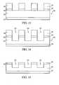
- FIG. 10a diagrammatic cross-sectional view of a semiconductor wafer according to a second embodiment of the present invention at an intermediate stage of processing.
- FIG. 11is a diagrammatic cross-sectional view of a semiconductor wafer according to the present invention subsequent to that shown in FIG. 10 .
- FIG. 12is a diagrammatic cross-sectional view of a semiconductor wafer according to the present invention subsequent to that shown in FIG. 11 .
- FIG. 13is a diagrammatic cross-sectional view of a semiconductor wafer according to the present invention subsequent to that shown in FIG. 12 .
- FIG. 14is a diagrammatic cross-sectional view of a semiconductor wafer according to the present invention subsequent to that shown in FIG. 13 .
- FIG. 15is a diagrammatic cross-sectional view of a semiconductor wafer according to the present invention subsequent to that shown in FIG. 14 .
- waferor “substrate” used in the following description may include any semiconductor-based structure that has an exposed silicon surface. Wafer and structure must be understood to include silicon-on insulator (SOI), silicon-on sapphire (SOS), doped and undoped semiconductors, epitaxial layers of silicon supported by a base semiconductor foundation, and other semiconductor structures.
- SOIsilicon-on insulator
- SOSsilicon-on sapphire
- the semiconductorneed not be silicon-based.
- the semiconductorcould be silicon-germanium, germanium, or gallium arsenide.
- the present inventionrelates to a method for plasma etching a semiconductor substrate which includes adding a low power strike step before the main plasma etching.
- the methodreduces striations formed in the substrate and decreases the CD loss.
- the present inventionis an improved plasma etching process in a high-density-source plasma reactor, i.e., one which uses a remote source to generate a plasma and which also uses a high-frequency bias power on the substrate.
- a high-density-source plasma reactori.e., one which uses a remote source to generate a plasma and which also uses a high-frequency bias power on the substrate.
- the photoresist lateral erosionis slowed while the resist is cured by UV radiation from the low power plasma.
- This additional stephas been shown to decreases the CD loss by about 400 Angstroms and also reduce the striations in the etched semiconductor substrate.
- Plasma etch systemsare mainly vacuum chambers in which a glow discharge produces a plasma consisting of chemically reactive species such as atoms, radicals, and ions from a relatively inert molecular gas. These reactive species interact either kinetically or chemically with the material to be etched.
- the plasma etching gasmay be any gaseous material known for etching. Examples of suitable plasma etching gases are those such as HBr, Cl, fluorocarbon containing gases and the like. It should be understood that the selection of the plasma etching gas will be determined by the substrate to the etched as well as the physical parameters of the etching process such as power, pressure, temperature and the like.
- etching gasexamples include: HBr, Cl 2 carbon tetrafluoride (CF 4 ) trifluoromethane (CHF3) and the like.
- the etching gasmay be used alone or in combination with other etching gases and may also be used in conjunction with an inert gas, such as argon or helium, to dilute the etching gases and to enhance the uniformity of the surface being etched.
- the etching process of the present inventionis carried out in a high density plasma (HDP) reactor such as an enhanced reactive ion etch.
- a reactive ion etchis a combination of chemical plasma etching, in which a plasma etches by chemically reacting with the substrate, and ion beam etching, which is a physical process using high energy ions to bombard the substrate in order to etch it.
- An explanation of plasma etching techniquesmay be found in U.S. Pat. No. 5,662,770 and U.S. Pat. No. 5,843,226 which are herein incorporated by reference.
- FIGS. 3-4A representative substrate etched according to the present invention is illustrated in FIGS. 3-4 .
- These figuresshow a wafer 100 formed of a substrate 116 having an oxide layer 118 which has cylindrical contact holes 110 , 112 , 114 formed therein by the method of the present invention as described in more detail below.
- the contact holes 110 , 112 , 114have a uniform shape and the critical dimension between the contact holes 110 , 112 , 114 is maintained.
- a photoresist layer 120is applied over a substrate 100 .
- a UV mask 122is placed over the photoresist layer 120 .
- the mask 122has areas 124 which allow UV light 128 to pass through and contact the photoresist layer 120 .
- the maskalso includes areas 126 which block the UV light 128 from contacting the photoresist layer 120 .
- the UV light 128contacts the photoresist layer 120 and develops the photoresist layer 120 under regions 124 of the UV mask 122 leaving developed photoresist areas 130 as shown in FIG. 6 .
- the UV lightcauses the exposed photoresist 130 to undergo chemical changes and become more acidic.
- the exposed (acidic) photoresist layer 130is removed with a base solution leaving the structure as shown in FIG. 7 . Since the photoresist layer 120 is substantially resistant to etching, certain portions of the substrate 116 covered by the photoresist patterns 120 are substantially not etched during the etching of the substrate.
- the substrateis then placed in a plasma reactor.
- the substrateis contacted with a low power plasma and the lateral erosion of the photoresist layer 120 is slowed while the photoresist layer 120 is cured by UV radiation from the low power plasma.
- the substrateis contacted with the low power plasma in the plasma reactor for about 3 to about 10 seconds, preferably for about 5 seconds.
- the plasma etching gasmay be any gaseous material known for etching.
- suitable plasma etching gasesare those such as HBr, Cl, fluorocarbon containing gases and the like. It should be understood that the selection of the plasma etching gas will be determined by the substrate to the etched as well as the physical parameters of the etching process such as power, pressure, temperature and the like. Examples of some preferred gases for use with the present invention include: HBr, Cl 2 carbon tetrafluoride (CF 4 ) trifluoromethane (CHF3) and the like.
- the low power plasmais formed at low power, such as, for example, 100 to about 250 watts (RF), preferably about 150 watts.
- the plasma etching processuses a process gas that comprises a mixture of two fluorocarbons, preferably carbon tetrafluoride (CF 4 ) and trifluoromethane (CHF3).
- the etching gas mixtureflows into the reactor at a rate of approximately 50 standard cubic centimeters per minute (sccm) to form a plasma (glow discharge) over the substrate.
- a diluent gassuch as argon also flows into the reactor at approximately 80 sccm.
- the preferred pressure in the etch chamberis about 120 mTorr, and the preferred cathode temperature is about 20 degree(s) C.
- the substrate 116is then etched out by a directional etching process such as reactive ion etching. Etching is continued down to the level of the substrate to form a set of trenches 132 , 134 136 .
- the plasma etchingis carried out under ordinary high power etching conditions.
- the plasma etchmay be formed at a power of from about 800 to about 1100 watts (RF), preferably at from about 950 watts.
- RFwatts
- Any suitable etching gasmay be used in accordance with the present invention.
- the same etching gases used in the low power plasma etching stepare used in the high power plasma etching.
- the plasma etching parameterssuch as gas composition, reactor pressure and the like do not need to be modified.
- the substratecan be contacted with the high power etch for any time sufficient to etch the underlying substrate. It should be understood that these times may vary from about 30 seconds to over 500 seconds, depending upon the substrate, the etching gas and the physical parameters of the plasma etch.
- the additional photoresist 120is then removed from the substrate 116 to arrive at the device shown in FIG. 9 .
- the photoresist layer 120must be robust enough to withstand reactive ion etching. However, due to enhanced ion bombardment near the trench 132 , 134 , 136 corners, the photoresist layer 120 becomes thinner and softer and it looses its resistance to chemical etching when exposed to UV light.
- the present inventioncures the photoresist layer 120 with a low power plasma etch step reducing the lateral erosion of the photoresist layer 120 . This additional low power strike eliminates striation in the trench walls and has been found to reduce CD loss by 400 angstroms.
- the inventionis further explained with reference to the following example. This invention is not intended to be limited by the particular example described below.
- the Exampleis also described with reference to FIGS. 10-15 .
- a combination of the following set of initial etch parameters in the first four steps of the plasma etching processmay be used.
- a wafer 200including a substrate 216 having formed thereon an oxide layer 218 and a bottom antireflective coating (BARC) layer 202 .
- a photoresist layer 220is applied over a substrate 200 .
- a UV mask 222is placed over the photoresist layer 220 .
- the mask 222has areas 224 which allow UV light 228 to pass through and contact the photoresist layer 220 .
- the maskalso includes areas 226 which block the UV light 228 from contacting the photoresist layer 220 .
- the UV light 228contacts the photoresist layer 220 and develops the photoresist layer 220 under regions 224 of the UV mask 222 leaving developed photoresist areas 230 as shown in FIG. 11 .
- the exposed (acidic) photoresist layer 230is removed with a base solution leaving the structure as shown in FIG. 12 .
- the substrate 200is then placed in a plasma reactor and allowed to stabilize at the following conditions for about 10 seconds: Pressure: 120 mTorr RF Power: 0 Watts Magnetic Field: 0 Gauss Cathode Temperature: 20 Celsius Gas flows: CF 4 50 sccm CHF 3 50 sccm Ar 80 sccm
- the substrate 200is then contacted with a low power plasma under the following conditions for about 5 seconds: Pressure: 120 mTorr RF Power: 150 Watts, AUTO Magnetic Field: 0 Gauss Cathode Temperature: 20 Celsius Gas flows: CF 4 50 sccm CHF 3 50 sccm Ar 80 sccm
- BARC layer 202is plasma etched under the following conditions for about 60 seconds: Pressure: 120 mTorr RF Power: 950 Watts, AUTO Magnetic Field: 0 Gauss Cathode Temperature: 20 Celsius Gas flows: CF 4 50 sccm CHF 3 50 sccm Ar 80 sccm
- oxide layer 218is etched in an oxide main etch step to form trenches 232 , 234 and 236 .
- the oxide layer 218is plasma etched under the following conditions for about 280 seconds: Pressure 120 mTorr RF Power: 950 Watts, AUTO Magnetic Field: 0 Gauss Cathode Temperature: 20 Celsius Gas flows: CF 4 15 sccm CHF 3 80 sccm Ar 140 sccm
- the photoresist layer 220is removed with subsequent processing and the resultant substrate 200 is illustrated in FIG. 15 .
- the striations in the substrate 200are significantly reduced, and the CD loss is reduced by about 400 Angstroms compared to a similar process without the low power plasma etch.
Landscapes
- Engineering & Computer Science (AREA)
- Physics & Mathematics (AREA)
- General Physics & Mathematics (AREA)
- Manufacturing & Machinery (AREA)
- Condensed Matter Physics & Semiconductors (AREA)
- Chemical & Material Sciences (AREA)
- Computer Hardware Design (AREA)
- Microelectronics & Electronic Packaging (AREA)
- Power Engineering (AREA)
- Inorganic Chemistry (AREA)
- Organic Chemistry (AREA)
- Chemical Kinetics & Catalysis (AREA)
- General Chemical & Material Sciences (AREA)
- Drying Of Semiconductors (AREA)
Abstract
Description
- The present invention relates to the fabrication of integrated circuit devices and, in particular, to a method for controlling striations and CD loss in the integrated circuit during an etching process.
- Semiconductor integrated circuits are typically fabricated on a wafer or substrate of a semiconductor material such as, for example, silicon or gallium arsenide. During the fabrication, the wafer is subjected to a sequence of steps, which may include photomasking, material deposition, oxidation, nitridization, ion implantation, diffusion, and etching, among others.
- Etching may be achieved by wet etching processes or dry etching processes. Dry etch processes, such as a plasma etch or ion-assisted etch, are known for etching materials for semiconductor fabrication in silicon integrated circuit technology. Plasma etches are largely anisotropic or unidirectional. Plasma etches may be used to create spaces or substantially vertical sidewalls in the integrated circuit layers, to transfer a mask pattern to an underlying layer with little or no undercutting beneath mask segment edges and to create contact paths in insulative layers. Plasma etch processes are especially useful for producing sub-quarter micrometer patterns and geometries.
- Semiconductor integrated circuits with high device density require the patterning of closely spaced submicrometer lines in semiconductors materials to form submicron geometries such as small area emitters for bipolar transistors, short gates for field effect transistors and narrow interconnection lines between devices. The formation of such polysilicon, metal or insulator structures typically requires definition of the locations of such structures in a layer of photoresist on a layer of polysilicon or insulator by exposure of the photoresist with light passing through a reticle or photomask containing the desired pattern. After exposure and treatment of the photoresist, the underlying layer of the substrate is plasma etched using the patterned photoresist as a template. The masking material protects designated areas of the substrate from the etch process. Subsequent processing steps are determined according to the type of device to be fabricated.
- As advances in photolithographic and processing capabilities progressively increase, the lateral dimensions of features in silicon integrated circuits continue to decrease. Fabrication of reduced device geometries in integrated circuits mandates minute contact holes of submicron size on insulation layers and minimum isolation distance requirements measured in terms of critical dimensions (CD). For example, recent generations of complementary metal-oxide silicon integrated circuits (CMOS) have gate regions with dimensions on the order of 0.25 microns, or even 0.18 microns and less in the near future.
- As the integrated circuit manufacture goes to the sub-quarter regime, a challenge to the high aspect ratio is that the deep ultraviolet (DUV) resist needed to pattern the integrated circuit is thinner and more malleable than prior photoresists. Large striations and uncontrolled increases in the size of the contact holes, known as CD losses, are common during the photolithographic process in the sub-quarter micron regime.
- During photolithography, problems arise because high resolution submicrometer images in photoresist require shallow depth of focus during exposure, but thick photoresist patterns are required because of the poor etch rate between the photoresist and the underlying semiconductor layer. Additional problems occur because of the uncontrolled bake during the plasma etch processing. During this process, the substrate is exposed to ion and electron bombardment, UV light, X-rays, and scattered radiations. As a consequence, irregular topographies, distorted images and CD loss occurs during the exposure of the photoresist layer as shown in
FIGS. 1-2 . These figures illustrate a typical plasma etch of asilicon substrate 40 having anoxide layer 42 deposited thereon. Contactholes wafer 10. Thecontact holes upper surface 38 and alower surface 36. Due, in part, to the thin DUV resist and the uncontrolled bake during the etching process,discontinuities contact hole 10. Thediscontinuities contact hole contact holes first surface 32 and asecond surface 34 in thewall 44 of thecontact hole 12. In addition,contact holes oxide layer 42. - When two
discontinuities adjacent contact holes contact holes contact holes - A further problem with the prior plasma etching is that as a result of the
irregular contact holes contact holes - Several attempts have been made to solve this problem. It has been suggested that the distorted images can be alleviated by employing a three-layer photoresist technique such as in U.S. Pat. No. 5,242,532 (Cain) or by employing a silylation layer process such as in U.S. Pat. No. 5,312,717 (Sachdev et al.). These solutions, however, require additional time consuming and costly steps in the etching process.
- Accordingly, there is a need for improved plasma etching that provides a substantially uniform etch without a reduction in the critical dimension and without striations formed in the sidewalls of the etched portion of the substrate. The improved plasma etching technique should provide a substrate having increased uniformity across the substrate surface, a substantially uniform trench, a substantially uniform profile angle and a smooth sidewall.
- The present invention provides a plasma etching process that reduces the striations and the CD loss between two contact holes in a substrate. The present invention provides an etching process in which the substrate of semiconductor material to be etched is formed with a substantially uniform etch without a reduction in the critical dimension and without striations formed in the sidewalls. The method of the present invention includes exposing a substrate to be etched to a first plasma under low-power, preferably at about radio frequency (RF) 150 W and then subsequently contacting the substrate to a conventional high power etch, preferably at about RF 950 W. Additional advantages of the present invention will be apparent from the detailed description and drawings, which illustrate preferred embodiments of the invention.
FIG. 1 is a top view of a semiconductor having three contact holes etched therein according to a method the present invention overcomes.FIG. 2 is a partial cross-sectional view taken along line II-II ofFIG. 1 .FIG. 3 is a top view of a semiconductor having three contact holes etched therein according to the present invention.FIG. 4 is a cross-sectional view taken along the line IV-IV ofFIG. 3 .FIG. 5 a diagrammatic cross-sectional view of a semiconductor wafer according to the present invention at an intermediate stage of processing.FIG. 6 is a diagrammatic cross-sectional view of a semiconductor wafer according to the present invention subsequent to that shown inFIG. 5 .FIG. 7 is a diagrammatic cross-sectional view of a semiconductor wafer according to the present invention subsequent to that shown inFIG. 6 .FIG. 8 is a diagrammatic cross-sectional view of a semiconductor wafer according to the present invention subsequent to that shown inFIG. 7 .FIG. 9 is a diagrammatic cross-sectional view of a semiconductor wafer according to the present invention subsequent to that shown inFIG. 8 .FIG. 10 adiagrammatic cross-sectional view of a semiconductor wafer according to a second embodiment of the present invention at an intermediate stage of processing.FIG. 11 is a diagrammatic cross-sectional view of a semiconductor wafer according to the present invention subsequent to that shown inFIG. 10 .FIG. 12 is a diagrammatic cross-sectional view of a semiconductor wafer according to the present invention subsequent to that shown inFIG. 11 .FIG. 13 is a diagrammatic cross-sectional view of a semiconductor wafer according to the present invention subsequent to that shown inFIG. 12 .FIG. 14 is a diagrammatic cross-sectional view of a semiconductor wafer according to the present invention subsequent to that shown inFIG. 13 .FIG. 15 is a diagrammatic cross-sectional view of a semiconductor wafer according to the present invention subsequent to that shown inFIG. 14 .- In the following detailed description, reference is made to various specific embodiments in which the invention may be practiced. These embodiments are described with sufficient detail to enable those skilled in the art to practice the invention, and it is to be understood that other embodiments may be employed, and that structural, logical, and electrical changes may be made.
- The terms “wafer” or “substrate” used in the following description may include any semiconductor-based structure that has an exposed silicon surface. Wafer and structure must be understood to include silicon-on insulator (SOI), silicon-on sapphire (SOS), doped and undoped semiconductors, epitaxial layers of silicon supported by a base semiconductor foundation, and other semiconductor structures. The semiconductor need not be silicon-based. The semiconductor could be silicon-germanium, germanium, or gallium arsenide. When reference is made to a wafer or substrate in the following description, previous process steps may have been utilized to form regions or junctions in the base semiconductor or foundation. The following detailed description may not be taken, therefore, in a limiting sense, and the scope of the present invention is defined by the appended claims.
- The present invention relates to a method for plasma etching a semiconductor substrate which includes adding a low power strike step before the main plasma etching. The method reduces striations formed in the substrate and decreases the CD loss. As discussed in more detail below, the present invention is an improved plasma etching process in a high-density-source plasma reactor, i.e., one which uses a remote source to generate a plasma and which also uses a high-frequency bias power on the substrate. During the low power strike, it is believed that the photoresist lateral erosion is slowed while the resist is cured by UV radiation from the low power plasma. This additional step has been shown to decreases the CD loss by about 400 Angstroms and also reduce the striations in the etched semiconductor substrate.
- Plasma etch systems are mainly vacuum chambers in which a glow discharge produces a plasma consisting of chemically reactive species such as atoms, radicals, and ions from a relatively inert molecular gas. These reactive species interact either kinetically or chemically with the material to be etched. The plasma etching gas may be any gaseous material known for etching. Examples of suitable plasma etching gases are those such as HBr, Cl, fluorocarbon containing gases and the like. It should be understood that the selection of the plasma etching gas will be determined by the substrate to the etched as well as the physical parameters of the etching process such as power, pressure, temperature and the like. Examples of some preferred gases for use with the present invention include: HBr, Cl2carbon tetrafluoride (CF4) trifluoromethane (CHF3) and the like. The etching gas may be used alone or in combination with other etching gases and may also be used in conjunction with an inert gas, such as argon or helium, to dilute the etching gases and to enhance the uniformity of the surface being etched.
- The etching process of the present invention is carried out in a high density plasma (HDP) reactor such as an enhanced reactive ion etch. A reactive ion etch is a combination of chemical plasma etching, in which a plasma etches by chemically reacting with the substrate, and ion beam etching, which is a physical process using high energy ions to bombard the substrate in order to etch it. An explanation of plasma etching techniques may be found in U.S. Pat. No. 5,662,770 and U.S. Pat. No. 5,843,226 which are herein incorporated by reference.
- Referring now to the drawings, where like elements are designated by like reference numerals. A representative substrate etched according to the present invention is illustrated in
FIGS. 3-4 . These figures show awafer 100 formed of asubstrate 116 having anoxide layer 118 which has cylindrical contact holes110,112,114 formed therein by the method of the present invention as described in more detail below. The contact holes110,112,114 have a uniform shape and the critical dimension between the contact holes110,112,114 is maintained. - Reference is now made to
FIG. 5 . Aphotoresist layer 120 is applied over asubstrate 100. AUV mask 122 is placed over thephotoresist layer 120. Themask 122 hasareas 124 which allowUV light 128 to pass through and contact thephotoresist layer 120. The mask also includesareas 126 which block the UV light128 from contacting thephotoresist layer 120. TheUV light 128 contacts thephotoresist layer 120 and develops thephotoresist layer 120 underregions 124 of theUV mask 122 leaving developedphotoresist areas 130 as shown inFIG. 6 . - The UV light causes the exposed
photoresist 130 to undergo chemical changes and become more acidic. After pattern generation, the exposed (acidic)photoresist layer 130 is removed with a base solution leaving the structure as shown inFIG. 7 . Since thephotoresist layer 120 is substantially resistant to etching, certain portions of thesubstrate 116 covered by thephotoresist patterns 120 are substantially not etched during the etching of the substrate. The substrate is then placed in a plasma reactor. The substrate is contacted with a low power plasma and the lateral erosion of thephotoresist layer 120 is slowed while thephotoresist layer 120 is cured by UV radiation from the low power plasma. The substrate is contacted with the low power plasma in the plasma reactor for about 3 to about 10 seconds, preferably for about 5 seconds. - The plasma etching gas may be any gaseous material known for etching. Examples of suitable plasma etching gases are those such as HBr, Cl, fluorocarbon containing gases and the like. It should be understood that the selection of the plasma etching gas will be determined by the substrate to the etched as well as the physical parameters of the etching process such as power, pressure, temperature and the like. Examples of some preferred gases for use with the present invention include: HBr, Cl2carbon tetrafluoride (CF4) trifluoromethane (CHF3) and the like. The low power plasma is formed at low power, such as, for example, 100 to about 250 watts (RF), preferably about 150 watts.
- According to a preferred embodiment, the plasma etching process uses a process gas that comprises a mixture of two fluorocarbons, preferably carbon tetrafluoride (CF4) and trifluoromethane (CHF3). The etching gas mixture flows into the reactor at a rate of approximately 50 standard cubic centimeters per minute (sccm) to form a plasma (glow discharge) over the substrate. A diluent gas such as argon also flows into the reactor at approximately 80 sccm. The preferred pressure in the etch chamber is about 120 mTorr, and the preferred cathode temperature is about 20 degree(s) C.
- Reference is now made to
FIG. 8 . Thesubstrate 116 is then etched out by a directional etching process such as reactive ion etching. Etching is continued down to the level of the substrate to form a set oftrenches substrate 116 without the need for additional time consuming processing steps. The substrate can be contacted with the high power etch for any time sufficient to etch the underlying substrate. It should be understood that these times may vary from about 30 seconds to over 500 seconds, depending upon the substrate, the etching gas and the physical parameters of the plasma etch. Theadditional photoresist 120 is then removed from thesubstrate 116 to arrive at the device shown inFIG. 9 . - As the etching process goes to the sub-quarter regime, the
photoresist layer 120 must be robust enough to withstand reactive ion etching. However, due to enhanced ion bombardment near thetrench photoresist layer 120 becomes thinner and softer and it looses its resistance to chemical etching when exposed to UV light. The present invention cures thephotoresist layer 120 with a low power plasma etch step reducing the lateral erosion of thephotoresist layer 120. This additional low power strike eliminates striation in the trench walls and has been found to reduce CD loss by 400 angstroms. - The invention is further explained with reference to the following example. This invention is not intended to be limited by the particular example described below. The Example is also described with reference to
FIGS. 10-15 . As a preferred embodiment, a combination of the following set of initial etch parameters in the first four steps of the plasma etching process may be used. - Reference is made to
FIG. 10 . Awafer 200 including asubstrate 216 having formed thereon anoxide layer 218 and a bottom antireflective coating (BARC)layer 202. Aphotoresist layer 220 is applied over asubstrate 200. AUV mask 222 is placed over thephotoresist layer 220. Themask 222 hasareas 224 which allowUV light 228 to pass through and contact thephotoresist layer 220. The mask also includesareas 226 which block the UV light228 from contacting thephotoresist layer 220. TheUV light 228 contacts thephotoresist layer 220 and develops thephotoresist layer 220 underregions 224 of theUV mask 222 leaving developedphotoresist areas 230 as shown inFIG. 11 . After pattern generation, the exposed (acidic)photoresist layer 230 is removed with a base solution leaving the structure as shown inFIG. 12 . - The
substrate 200 is then placed in a plasma reactor and allowed to stabilize at the following conditions for about 10 seconds:Pressure: 120 mTorr RF Power: 0 Watts Magnetic Field: 0 Gauss Cathode Temperature: 20 Celsius Gas flows: CF4 50 sccm CHF3 50 sccm Ar 80 sccm - The
substrate 200 is then contacted with a low power plasma under the following conditions for about 5 seconds:Pressure: 120 mTorr RF Power: 150 Watts, AUTO Magnetic Field: 0 Gauss Cathode Temperature: 20 Celsius Gas flows: CF4 50 sccm CHF3 50 sccm Ar 80 sccm - Reference is now made to
FIG. 13 . After the low power plasma etch,BARC layer 202 is plasma etched under the following conditions for about 60 seconds:Pressure: 120 mTorr RF Power: 950 Watts, AUTO Magnetic Field: 0 Gauss Cathode Temperature: 20 Celsius Gas flows: CF4 50 sccm CHF3 50 sccm Ar 80 sccm - Reference is now made to
FIG. 14 . After the BARC etch,oxide layer 218 is etched in an oxide main etch step to formtrenches oxide layer 218 is plasma etched under the following conditions for about 280 seconds:Pressure 120 mTorr RF Power: 950 Watts, AUTO Magnetic Field: 0 Gauss Cathode Temperature: 20 Celsius Gas flows: CF4 15 sccm CHF3 80 sccm Ar 140 sccm - The
photoresist layer 220 is removed with subsequent processing and theresultant substrate 200 is illustrated inFIG. 15 . By adding a low power strike before the BARC etch, the striations in thesubstrate 200 are significantly reduced, and the CD loss is reduced by about 400 Angstroms compared to a similar process without the low power plasma etch. - The above description illustrates preferred embodiments which achieve the objects, features and advantages of the present invention. It is not intended that the present invention be limited to the illustrated embodiments. Any modification of the present invention that comes within the spirit and scope of the following claims should be considered part of the present invention.
Claims (47)
Priority Applications (3)
| Application Number | Priority Date | Filing Date | Title |
|---|---|---|---|
| US10/969,568US7122480B2 (en) | 1999-04-15 | 2004-10-21 | Method of plasma etching a substrate |
| US11/418,256US7470625B2 (en) | 1999-04-15 | 2006-05-05 | Method of plasma etching a substrate |
| US12/326,834US8093155B2 (en) | 1999-04-15 | 2008-12-02 | Method of controlling striations and CD loss in contact oxide etch |
Applications Claiming Priority (3)
| Application Number | Priority Date | Filing Date | Title |
|---|---|---|---|
| US09/292,393US6335292B1 (en) | 1999-04-15 | 1999-04-15 | Method of controlling striations and CD loss in contact oxide etch |
| US09/902,691US20010050413A1 (en) | 1999-04-15 | 2001-07-12 | Method of controlling striations and CD loss in contact oxide etch |
| US10/969,568US7122480B2 (en) | 1999-04-15 | 2004-10-21 | Method of plasma etching a substrate |
Related Parent Applications (1)
| Application Number | Title | Priority Date | Filing Date |
|---|---|---|---|
| US09/902,691ContinuationUS20010050413A1 (en) | 1999-04-15 | 2001-07-12 | Method of controlling striations and CD loss in contact oxide etch |
Related Child Applications (1)
| Application Number | Title | Priority Date | Filing Date |
|---|---|---|---|
| US11/418,256ContinuationUS7470625B2 (en) | 1999-04-15 | 2006-05-05 | Method of plasma etching a substrate |
Publications (2)
| Publication Number | Publication Date |
|---|---|
| US20050056875A1true US20050056875A1 (en) | 2005-03-17 |
| US7122480B2 US7122480B2 (en) | 2006-10-17 |
Family
ID=23124481
Family Applications (7)
| Application Number | Title | Priority Date | Filing Date |
|---|---|---|---|
| US09/292,393Expired - Fee RelatedUS6335292B1 (en) | 1999-04-15 | 1999-04-15 | Method of controlling striations and CD loss in contact oxide etch |
| US09/902,691AbandonedUS20010050413A1 (en) | 1999-04-15 | 2001-07-12 | Method of controlling striations and CD loss in contact oxide etch |
| US09/939,651Expired - LifetimeUS6753264B2 (en) | 1999-04-15 | 2001-08-28 | Method of controlling striations and CD loss in contact oxide etch |
| US09/991,982Expired - LifetimeUS6716763B2 (en) | 1999-04-15 | 2001-11-26 | Method of controlling striations and CD loss in contact oxide etch |
| US10/969,568Expired - Fee RelatedUS7122480B2 (en) | 1999-04-15 | 2004-10-21 | Method of plasma etching a substrate |
| US11/418,256Expired - Fee RelatedUS7470625B2 (en) | 1999-04-15 | 2006-05-05 | Method of plasma etching a substrate |
| US12/326,834Expired - Fee RelatedUS8093155B2 (en) | 1999-04-15 | 2008-12-02 | Method of controlling striations and CD loss in contact oxide etch |
Family Applications Before (4)
| Application Number | Title | Priority Date | Filing Date |
|---|---|---|---|
| US09/292,393Expired - Fee RelatedUS6335292B1 (en) | 1999-04-15 | 1999-04-15 | Method of controlling striations and CD loss in contact oxide etch |
| US09/902,691AbandonedUS20010050413A1 (en) | 1999-04-15 | 2001-07-12 | Method of controlling striations and CD loss in contact oxide etch |
| US09/939,651Expired - LifetimeUS6753264B2 (en) | 1999-04-15 | 2001-08-28 | Method of controlling striations and CD loss in contact oxide etch |
| US09/991,982Expired - LifetimeUS6716763B2 (en) | 1999-04-15 | 2001-11-26 | Method of controlling striations and CD loss in contact oxide etch |
Family Applications After (2)
| Application Number | Title | Priority Date | Filing Date |
|---|---|---|---|
| US11/418,256Expired - Fee RelatedUS7470625B2 (en) | 1999-04-15 | 2006-05-05 | Method of plasma etching a substrate |
| US12/326,834Expired - Fee RelatedUS8093155B2 (en) | 1999-04-15 | 2008-12-02 | Method of controlling striations and CD loss in contact oxide etch |
Country Status (1)
| Country | Link |
|---|---|
| US (7) | US6335292B1 (en) |
Families Citing this family (35)
| Publication number | Priority date | Publication date | Assignee | Title |
|---|---|---|---|---|
| US6335292B1 (en)* | 1999-04-15 | 2002-01-01 | Micron Technology, Inc. | Method of controlling striations and CD loss in contact oxide etch |
| US6933243B2 (en)* | 2002-02-06 | 2005-08-23 | Applied Materials, Inc. | High selectivity and residue free process for metal on thin dielectric gate etch application |
| ITMI20020931A1 (en)* | 2002-05-02 | 2003-11-03 | St Microelectronics Srl | METHOD FOR MANUFACTURING INTEGRATED ELECTRONIC CIRCUITS ON A SEMICONDUCTIVE SUBSTRATE |
| US6923920B2 (en)* | 2002-08-14 | 2005-08-02 | Lam Research Corporation | Method and compositions for hardening photoresist in etching processes |
| AU2003299368A1 (en)* | 2002-12-20 | 2004-07-22 | S.O.I. Tec Silicon On Insulator Technologies | Method of the production of cavities in a silicon sheet |
| FR2849269B1 (en)* | 2002-12-20 | 2005-07-29 | Soitec Silicon On Insulator | METHOD FOR PRODUCING CAVITIES IN A SILICON PLATE |
| US7060626B2 (en)* | 2003-06-25 | 2006-06-13 | International Business Machines Corporation | Multi-run selective pattern and etch wafer process |
| KR20050070837A (en)* | 2003-12-31 | 2005-07-07 | 동부아남반도체 주식회사 | Etching method for preventing plasma damage in metal oxide semiconductor device |
| US7712434B2 (en)* | 2004-04-30 | 2010-05-11 | Lam Research Corporation | Apparatus including showerhead electrode and heater for plasma processing |
| US8317968B2 (en) | 2004-04-30 | 2012-11-27 | Lam Research Corporation | Apparatus including gas distribution member supplying process gas and radio frequency (RF) power for plasma processing |
| US7615164B2 (en)* | 2004-06-23 | 2009-11-10 | Micron Technology, Inc. | Plasma etching methods and contact opening forming methods |
| FR2875947B1 (en)* | 2004-09-30 | 2007-09-07 | Tracit Technologies | NOVEL STRUCTURE FOR MICROELECTRONICS AND MICROSYSTEMS AND METHOD OF MAKING SAME |
| FR2876220B1 (en)* | 2004-10-06 | 2007-09-28 | Commissariat Energie Atomique | METHOD FOR PRODUCING MIXED STACKED STRUCTURES, VARIOUS INSULATING AREAS AND / OR LOCALIZED VERTICAL ELECTRICAL CONDUCTION ZONES. |
| US20060094237A1 (en)* | 2004-10-29 | 2006-05-04 | Taiwan Semiconductor Manufacturing Co., Ltd. | Methods to completely eliminate or significantly reduce defects in copper metallization in IC manufacturing |
| FR2897982B1 (en) | 2006-02-27 | 2008-07-11 | Tracit Technologies Sa | METHOD FOR MANUFACTURING PARTIALLY-LIKE STRUCTURES, COMPRISING AREAS CONNECTING A SURFACE LAYER AND A SUBSTRATE |
| US7494933B2 (en)* | 2006-06-16 | 2009-02-24 | Synopsys, Inc. | Method for achieving uniform etch depth using ion implantation and a timed etch |
| KR100853789B1 (en)* | 2006-11-27 | 2008-08-25 | 동부일렉트로닉스 주식회사 | Semiconductor device and manufacturing method thereof |
| US7838432B2 (en)* | 2007-04-16 | 2010-11-23 | Applied Materials, Inc. | Etch process with controlled critical dimension shrink |
| US7981812B2 (en)* | 2007-07-08 | 2011-07-19 | Applied Materials, Inc. | Methods for forming ultra thin structures on a substrate |
| US8343305B2 (en) | 2007-09-04 | 2013-01-01 | Lam Research Corporation | Method and apparatus for diagnosing status of parts in real time in plasma processing equipment |
| US20100330805A1 (en)* | 2007-11-02 | 2010-12-30 | Kenny Linh Doan | Methods for forming high aspect ratio features on a substrate |
| US20090174036A1 (en)* | 2008-01-04 | 2009-07-09 | International Business Machines Corporation | Plasma curing of patterning materials for aggressively scaled features |
| US20090191711A1 (en)* | 2008-01-30 | 2009-07-30 | Ying Rui | Hardmask open process with enhanced cd space shrink and reduction |
| US8298958B2 (en)* | 2008-07-17 | 2012-10-30 | Lam Research Corporation | Organic line width roughness with H2 plasma treatment |
| TWI398022B (en)* | 2010-03-17 | 2013-06-01 | Univ Nat Chunghsing | Separation method of epitaxial substrate of photovoltaic element |
| US20120305525A1 (en)* | 2011-05-31 | 2012-12-06 | Hsiu-Chun Lee | Method of reducing striation on a sidewall of a recess |
| US8529776B2 (en) | 2011-07-25 | 2013-09-10 | Applied Materials, Inc. | High lateral to vertical ratio etch process for device manufacturing |
| US8841742B2 (en) | 2011-09-27 | 2014-09-23 | Soitec | Low temperature layer transfer process using donor structure with material in recesses in transfer layer, semiconductor structures fabricated using such methods |
| TWI422422B (en)* | 2011-11-09 | 2014-01-11 | Nat Univ Tsing Hua | Electrocatalytic converter for exhaust emission control |
| CN103377885B (en)* | 2012-04-27 | 2016-03-16 | 南亚科技股份有限公司 | method of opening |
| US9269587B2 (en) | 2013-09-06 | 2016-02-23 | Applied Materials, Inc. | Methods for etching materials using synchronized RF pulses |
| US9419107B2 (en) | 2014-06-19 | 2016-08-16 | Applied Materials, Inc. | Method for fabricating vertically stacked nanowires for semiconductor applications |
| US9640385B2 (en) | 2015-02-16 | 2017-05-02 | Applied Materials, Inc. | Gate electrode material residual removal process |
| US9496148B1 (en) | 2015-09-10 | 2016-11-15 | International Business Machines Corporation | Method of charge controlled patterning during reactive ion etching |
| US11114306B2 (en) | 2018-09-17 | 2021-09-07 | Applied Materials, Inc. | Methods for depositing dielectric material |
Citations (32)
| Publication number | Priority date | Publication date | Assignee | Title |
|---|---|---|---|---|
| US4554048A (en)* | 1984-10-17 | 1985-11-19 | At&T Bell Laboratories | Anistropic etching |
| US4908095A (en)* | 1988-05-02 | 1990-03-13 | Tokyo Electron Limited | Etching device, and etching method |
| US4920070A (en)* | 1987-02-19 | 1990-04-24 | Fujitsu Limited | Method for forming wirings for a semiconductor device by filling very narrow via holes |
| US5008212A (en)* | 1988-12-12 | 1991-04-16 | Chen Teh Yi J | Selective asperity definition technique suitable for use in fabricating floating-gate transistor |
| US5021121A (en)* | 1990-02-16 | 1991-06-04 | Applied Materials, Inc. | Process for RIE etching silicon dioxide |
| US5102815A (en)* | 1990-12-19 | 1992-04-07 | Intel Corporation | Method of fabricating a composite inverse T-gate metal oxide semiconductor device |
| US5242532A (en)* | 1992-03-20 | 1993-09-07 | Vlsi Technology, Inc. | Dual mode plasma etching system and method of plasma endpoint detection |
| US5242536A (en)* | 1990-12-20 | 1993-09-07 | Lsi Logic Corporation | Anisotropic polysilicon etching process |
| US5312717A (en)* | 1992-09-24 | 1994-05-17 | International Business Machines Corporation | Residue free vertical pattern transfer with top surface imaging resists |
| US5441596A (en)* | 1994-07-27 | 1995-08-15 | Cypress Semiconductor Corporation | Method for forming a stable plasma |
| US5451290A (en)* | 1989-08-14 | 1995-09-19 | Applied Materials, Inc. | Gas distribution system |
| US5474648A (en)* | 1994-07-29 | 1995-12-12 | Lsi Logic Corporation | Uniform and repeatable plasma processing |
| US5612514A (en)* | 1993-09-30 | 1997-03-18 | Atmel Corporation | Tab test device for area array interconnected chips |
| US5612574A (en)* | 1995-06-06 | 1997-03-18 | Texas Instruments Incorporated | Semiconductor structures using high-dielectric-constant materials and an adhesion layer |
| US5662770A (en)* | 1993-04-16 | 1997-09-02 | Micron Technology, Inc. | Method and apparatus for improving etch uniformity in remote source plasma reactors with powered wafer chucks |
| US5710067A (en)* | 1995-06-07 | 1998-01-20 | Advanced Micro Devices, Inc. | Silicon oxime film |
| US5726499A (en)* | 1995-07-22 | 1998-03-10 | Ricoh Company, Ltd. | Semiconductor device having a minute contact hole |
| US5843266A (en)* | 1995-05-26 | 1998-12-01 | Owens Corning Fiberglas Technology, Inc. | Formable reinforcing bar and method for making same |
| US5843226A (en)* | 1996-07-16 | 1998-12-01 | Applied Materials, Inc. | Etch process for single crystal silicon |
| US5998302A (en)* | 1997-01-31 | 1999-12-07 | Sony Corporation | Method of manufacturing semiconductor device |
| US5998868A (en)* | 1998-02-04 | 1999-12-07 | International Business Machines Corporation | Very dense chip package |
| US6054377A (en)* | 1997-05-19 | 2000-04-25 | Motorola, Inc. | Method for forming an inlaid via in a semiconductor device |
| US6057227A (en)* | 1997-06-23 | 2000-05-02 | Vlsi Technology, Inc. | Oxide etch stop techniques for uniform damascene trench depth |
| US6074959A (en)* | 1997-09-19 | 2000-06-13 | Applied Materials, Inc. | Method manifesting a wide process window and using hexafluoropropane or other hydrofluoropropanes to selectively etch oxide |
| US6083844A (en)* | 1997-12-22 | 2000-07-04 | Lam Research Corporation | Techniques for etching an oxide layer |
| US6159794A (en)* | 1998-05-12 | 2000-12-12 | Advanced Micro Devices, Inc. | Methods for removing silicide residue in a semiconductor device |
| US6162696A (en)* | 1997-11-10 | 2000-12-19 | Intel Corporation | Method of fabricating a feature in an integrated circuit using a two mask process with a single edge definition layer |
| US6180533B1 (en)* | 1999-08-10 | 2001-01-30 | Applied Materials, Inc. | Method for etching a trench having rounded top corners in a silicon substrate |
| US6335292B1 (en)* | 1999-04-15 | 2002-01-01 | Micron Technology, Inc. | Method of controlling striations and CD loss in contact oxide etch |
| US6355557B2 (en)* | 1998-07-22 | 2002-03-12 | Applied Materials, Inc. | Oxide plasma etching process with a controlled wineglass shape |
| US6426016B1 (en)* | 1999-07-30 | 2002-07-30 | Mosel Vitelic Inc. | Method for etching passivation layers and antireflective layer on a substrate |
| US6489632B1 (en)* | 1993-01-18 | 2002-12-03 | Semiconductor Energy Laboratory Co., Ltd. | Semiconductor device having a gate oxide film |
Family Cites Families (5)
| Publication number | Priority date | Publication date | Assignee | Title |
|---|---|---|---|---|
| US5976986A (en)* | 1996-08-06 | 1999-11-02 | International Business Machines Corp. | Low pressure and low power C12 /HC1 process for sub-micron metal etching |
| JPH1140683A (en) | 1997-07-22 | 1999-02-12 | Hitachi Ltd | Semiconductor memory device and method of manufacturing the same |
| US6020091A (en)* | 1997-09-30 | 2000-02-01 | Siemens Aktiengesellschaft | Hard etch mask |
| TW473817B (en)* | 2000-01-11 | 2002-01-21 | Ibm | Method for eliminating development related defects in photoresist masks |
| US7119025B2 (en)* | 2004-04-08 | 2006-10-10 | Micron Technology, Inc. | Methods of eliminating pattern collapse on photoresist patterns |
- 1999
- 1999-04-15USUS09/292,393patent/US6335292B1/ennot_activeExpired - Fee Related
- 2001
- 2001-07-12USUS09/902,691patent/US20010050413A1/ennot_activeAbandoned
- 2001-08-28USUS09/939,651patent/US6753264B2/ennot_activeExpired - Lifetime
- 2001-11-26USUS09/991,982patent/US6716763B2/ennot_activeExpired - Lifetime
- 2004
- 2004-10-21USUS10/969,568patent/US7122480B2/ennot_activeExpired - Fee Related
- 2006
- 2006-05-05USUS11/418,256patent/US7470625B2/ennot_activeExpired - Fee Related
- 2008
- 2008-12-02USUS12/326,834patent/US8093155B2/ennot_activeExpired - Fee Related
Patent Citations (32)
| Publication number | Priority date | Publication date | Assignee | Title |
|---|---|---|---|---|
| US4554048A (en)* | 1984-10-17 | 1985-11-19 | At&T Bell Laboratories | Anistropic etching |
| US4920070A (en)* | 1987-02-19 | 1990-04-24 | Fujitsu Limited | Method for forming wirings for a semiconductor device by filling very narrow via holes |
| US4908095A (en)* | 1988-05-02 | 1990-03-13 | Tokyo Electron Limited | Etching device, and etching method |
| US5008212A (en)* | 1988-12-12 | 1991-04-16 | Chen Teh Yi J | Selective asperity definition technique suitable for use in fabricating floating-gate transistor |
| US5451290A (en)* | 1989-08-14 | 1995-09-19 | Applied Materials, Inc. | Gas distribution system |
| US5021121A (en)* | 1990-02-16 | 1991-06-04 | Applied Materials, Inc. | Process for RIE etching silicon dioxide |
| US5102815A (en)* | 1990-12-19 | 1992-04-07 | Intel Corporation | Method of fabricating a composite inverse T-gate metal oxide semiconductor device |
| US5242536A (en)* | 1990-12-20 | 1993-09-07 | Lsi Logic Corporation | Anisotropic polysilicon etching process |
| US5242532A (en)* | 1992-03-20 | 1993-09-07 | Vlsi Technology, Inc. | Dual mode plasma etching system and method of plasma endpoint detection |
| US5312717A (en)* | 1992-09-24 | 1994-05-17 | International Business Machines Corporation | Residue free vertical pattern transfer with top surface imaging resists |
| US6489632B1 (en)* | 1993-01-18 | 2002-12-03 | Semiconductor Energy Laboratory Co., Ltd. | Semiconductor device having a gate oxide film |
| US5662770A (en)* | 1993-04-16 | 1997-09-02 | Micron Technology, Inc. | Method and apparatus for improving etch uniformity in remote source plasma reactors with powered wafer chucks |
| US5612514A (en)* | 1993-09-30 | 1997-03-18 | Atmel Corporation | Tab test device for area array interconnected chips |
| US5441596A (en)* | 1994-07-27 | 1995-08-15 | Cypress Semiconductor Corporation | Method for forming a stable plasma |
| US5474648A (en)* | 1994-07-29 | 1995-12-12 | Lsi Logic Corporation | Uniform and repeatable plasma processing |
| US5843266A (en)* | 1995-05-26 | 1998-12-01 | Owens Corning Fiberglas Technology, Inc. | Formable reinforcing bar and method for making same |
| US5612574A (en)* | 1995-06-06 | 1997-03-18 | Texas Instruments Incorporated | Semiconductor structures using high-dielectric-constant materials and an adhesion layer |
| US5710067A (en)* | 1995-06-07 | 1998-01-20 | Advanced Micro Devices, Inc. | Silicon oxime film |
| US5726499A (en)* | 1995-07-22 | 1998-03-10 | Ricoh Company, Ltd. | Semiconductor device having a minute contact hole |
| US5843226A (en)* | 1996-07-16 | 1998-12-01 | Applied Materials, Inc. | Etch process for single crystal silicon |
| US5998302A (en)* | 1997-01-31 | 1999-12-07 | Sony Corporation | Method of manufacturing semiconductor device |
| US6054377A (en)* | 1997-05-19 | 2000-04-25 | Motorola, Inc. | Method for forming an inlaid via in a semiconductor device |
| US6057227A (en)* | 1997-06-23 | 2000-05-02 | Vlsi Technology, Inc. | Oxide etch stop techniques for uniform damascene trench depth |
| US6074959A (en)* | 1997-09-19 | 2000-06-13 | Applied Materials, Inc. | Method manifesting a wide process window and using hexafluoropropane or other hydrofluoropropanes to selectively etch oxide |
| US6162696A (en)* | 1997-11-10 | 2000-12-19 | Intel Corporation | Method of fabricating a feature in an integrated circuit using a two mask process with a single edge definition layer |
| US6083844A (en)* | 1997-12-22 | 2000-07-04 | Lam Research Corporation | Techniques for etching an oxide layer |
| US5998868A (en)* | 1998-02-04 | 1999-12-07 | International Business Machines Corporation | Very dense chip package |
| US6159794A (en)* | 1998-05-12 | 2000-12-12 | Advanced Micro Devices, Inc. | Methods for removing silicide residue in a semiconductor device |
| US6355557B2 (en)* | 1998-07-22 | 2002-03-12 | Applied Materials, Inc. | Oxide plasma etching process with a controlled wineglass shape |
| US6335292B1 (en)* | 1999-04-15 | 2002-01-01 | Micron Technology, Inc. | Method of controlling striations and CD loss in contact oxide etch |
| US6426016B1 (en)* | 1999-07-30 | 2002-07-30 | Mosel Vitelic Inc. | Method for etching passivation layers and antireflective layer on a substrate |
| US6180533B1 (en)* | 1999-08-10 | 2001-01-30 | Applied Materials, Inc. | Method for etching a trench having rounded top corners in a silicon substrate |
Also Published As
| Publication number | Publication date |
|---|---|
| US6753264B2 (en) | 2004-06-22 |
| US7122480B2 (en) | 2006-10-17 |
| US8093155B2 (en) | 2012-01-10 |
| US20060252198A1 (en) | 2006-11-09 |
| US6335292B1 (en) | 2002-01-01 |
| US20020019140A1 (en) | 2002-02-14 |
| US7470625B2 (en) | 2008-12-30 |
| US20010050413A1 (en) | 2001-12-13 |
| US20030096506A1 (en) | 2003-05-22 |
| US6716763B2 (en) | 2004-04-06 |
| US20090081877A1 (en) | 2009-03-26 |
Similar Documents
| Publication | Publication Date | Title |
|---|---|---|
| US8093155B2 (en) | Method of controlling striations and CD loss in contact oxide etch | |
| US6326307B1 (en) | Plasma pretreatment of photoresist in an oxide etch process | |
| US6716570B2 (en) | Low temperature resist trimming process | |
| US6362111B1 (en) | Tunable gate linewidth reduction process | |
| US6426300B2 (en) | Method for fabricating semiconductor device by using etching polymer | |
| US20070077724A1 (en) | Etching methods and apparatus and substrate assemblies produced therewith | |
| JPH08306672A (en) | Method of forming perpendicular sidewall | |
| JP2004031944A (en) | Forming method of very narrow width transistor gate element by photolithography | |
| US20060011579A1 (en) | Gas compositions | |
| US5167762A (en) | Anisotropic etch method | |
| KR100595090B1 (en) | Improved Etching Method Using Photoresist Mask | |
| JPH0945633A (en) | Method for forming fine hole of semiconductor integrated circuit device | |
| US6787455B2 (en) | Bi-layer photoresist method for forming high resolution semiconductor features | |
| KR19990050210A (en) | Oxide Etching Method | |
| JPH1098029A (en) | Processing method to etch organic anti-reflective coating from substrate | |
| US20020142486A1 (en) | Method of fabricating semiconductor device | |
| US6921723B1 (en) | Etching method having high silicon-to-photoresist selectivity | |
| US20020039704A1 (en) | Lithographic and etching process using a hardened photoresist layer | |
| JPH08288256A (en) | Trench etching method | |
| US20060105578A1 (en) | High-selectivity etching process | |
| KR100249012B1 (en) | Method for forming contact hole | |
| JPH09246246A (en) | Dry etching method and semiconductor device manufacturing method | |
| KR20000066421A (en) | Method of forming micro patterns for semiconductor devices | |
| KR20050022169A (en) | Method for forming isolation layer of semiconductor device | |
| KR20000026810A (en) | Method for forming micro pattern of semiconductor element |
Legal Events
| Date | Code | Title | Description |
|---|---|---|---|
| FPAY | Fee payment | Year of fee payment:4 | |
| FPAY | Fee payment | Year of fee payment:8 | |
| AS | Assignment | Owner name:U.S. BANK NATIONAL ASSOCIATION, AS COLLATERAL AGENT, CALIFORNIA Free format text:SECURITY INTEREST;ASSIGNOR:MICRON TECHNOLOGY, INC.;REEL/FRAME:038669/0001 Effective date:20160426 Owner name:U.S. BANK NATIONAL ASSOCIATION, AS COLLATERAL AGEN Free format text:SECURITY INTEREST;ASSIGNOR:MICRON TECHNOLOGY, INC.;REEL/FRAME:038669/0001 Effective date:20160426 | |
| AS | Assignment | Owner name:MORGAN STANLEY SENIOR FUNDING, INC., AS COLLATERAL AGENT, MARYLAND Free format text:PATENT SECURITY AGREEMENT;ASSIGNOR:MICRON TECHNOLOGY, INC.;REEL/FRAME:038954/0001 Effective date:20160426 Owner name:MORGAN STANLEY SENIOR FUNDING, INC., AS COLLATERAL Free format text:PATENT SECURITY AGREEMENT;ASSIGNOR:MICRON TECHNOLOGY, INC.;REEL/FRAME:038954/0001 Effective date:20160426 | |
| AS | Assignment | Owner name:U.S. BANK NATIONAL ASSOCIATION, AS COLLATERAL AGENT, CALIFORNIA Free format text:CORRECTIVE ASSIGNMENT TO CORRECT THE REPLACE ERRONEOUSLY FILED PATENT #7358718 WITH THE CORRECT PATENT #7358178 PREVIOUSLY RECORDED ON REEL 038669 FRAME 0001. ASSIGNOR(S) HEREBY CONFIRMS THE SECURITY INTEREST;ASSIGNOR:MICRON TECHNOLOGY, INC.;REEL/FRAME:043079/0001 Effective date:20160426 Owner name:U.S. BANK NATIONAL ASSOCIATION, AS COLLATERAL AGEN Free format text:CORRECTIVE ASSIGNMENT TO CORRECT THE REPLACE ERRONEOUSLY FILED PATENT #7358718 WITH THE CORRECT PATENT #7358178 PREVIOUSLY RECORDED ON REEL 038669 FRAME 0001. ASSIGNOR(S) HEREBY CONFIRMS THE SECURITY INTEREST;ASSIGNOR:MICRON TECHNOLOGY, INC.;REEL/FRAME:043079/0001 Effective date:20160426 | |
| FEPP | Fee payment procedure | Free format text:MAINTENANCE FEE REMINDER MAILED (ORIGINAL EVENT CODE: REM.) | |
| AS | Assignment | Owner name:MICRON TECHNOLOGY, INC., IDAHO Free format text:RELEASE BY SECURED PARTY;ASSIGNOR:U.S. BANK NATIONAL ASSOCIATION, AS COLLATERAL AGENT;REEL/FRAME:047243/0001 Effective date:20180629 | |
| LAPS | Lapse for failure to pay maintenance fees | Free format text:PATENT EXPIRED FOR FAILURE TO PAY MAINTENANCE FEES (ORIGINAL EVENT CODE: EXP.); ENTITY STATUS OF PATENT OWNER: LARGE ENTITY | |
| STCH | Information on status: patent discontinuation | Free format text:PATENT EXPIRED DUE TO NONPAYMENT OF MAINTENANCE FEES UNDER 37 CFR 1.362 | |
| FP | Lapsed due to failure to pay maintenance fee | Effective date:20181017 | |
| AS | Assignment | Owner name:MICRON TECHNOLOGY, INC., IDAHO Free format text:RELEASE BY SECURED PARTY;ASSIGNOR:MORGAN STANLEY SENIOR FUNDING, INC., AS COLLATERAL AGENT;REEL/FRAME:050937/0001 Effective date:20190731 |