US20050054216A1 - Methods of forming patterned photoresist layers over semiconductor substrates - Google Patents
Methods of forming patterned photoresist layers over semiconductor substratesDownload PDFInfo
- Publication number
- US20050054216A1 US20050054216A1US10/655,997US65599703AUS2005054216A1US 20050054216 A1US20050054216 A1US 20050054216A1US 65599703 AUS65599703 AUS 65599703AUS 2005054216 A1US2005054216 A1US 2005054216A1
- Authority
- US
- United States
- Prior art keywords
- treating
- basic
- treating fluid
- applying
- fluid
- Prior art date
- Legal status (The legal status is an assumption and is not a legal conclusion. Google has not performed a legal analysis and makes no representation as to the accuracy of the status listed.)
- Granted
Links
Images


Classifications
- H—ELECTRICITY
- H01—ELECTRIC ELEMENTS
- H01L—SEMICONDUCTOR DEVICES NOT COVERED BY CLASS H10
- H01L21/00—Processes or apparatus adapted for the manufacture or treatment of semiconductor or solid state devices or of parts thereof
- H01L21/02—Manufacture or treatment of semiconductor devices or of parts thereof
- H01L21/02104—Forming layers
- H01L21/02107—Forming insulating materials on a substrate
- H01L21/02296—Forming insulating materials on a substrate characterised by the treatment performed before or after the formation of the layer
- H01L21/02318—Forming insulating materials on a substrate characterised by the treatment performed before or after the formation of the layer post-treatment
- H01L21/02343—Forming insulating materials on a substrate characterised by the treatment performed before or after the formation of the layer post-treatment treatment by exposure to a liquid
- G—PHYSICS
- G03—PHOTOGRAPHY; CINEMATOGRAPHY; ANALOGOUS TECHNIQUES USING WAVES OTHER THAN OPTICAL WAVES; ELECTROGRAPHY; HOLOGRAPHY
- G03F—PHOTOMECHANICAL PRODUCTION OF TEXTURED OR PATTERNED SURFACES, e.g. FOR PRINTING, FOR PROCESSING OF SEMICONDUCTOR DEVICES; MATERIALS THEREFOR; ORIGINALS THEREFOR; APPARATUS SPECIALLY ADAPTED THEREFOR
- G03F7/00—Photomechanical, e.g. photolithographic, production of textured or patterned surfaces, e.g. printing surfaces; Materials therefor, e.g. comprising photoresists; Apparatus specially adapted therefor
- G03F7/004—Photosensitive materials
- G03F7/09—Photosensitive materials characterised by structural details, e.g. supports, auxiliary layers
- G03F7/091—Photosensitive materials characterised by structural details, e.g. supports, auxiliary layers characterised by antireflection means or light filtering or absorbing means, e.g. anti-halation, contrast enhancement
- H—ELECTRICITY
- H01—ELECTRIC ELEMENTS
- H01L—SEMICONDUCTOR DEVICES NOT COVERED BY CLASS H10
- H01L21/00—Processes or apparatus adapted for the manufacture or treatment of semiconductor or solid state devices or of parts thereof
- H01L21/02—Manufacture or treatment of semiconductor devices or of parts thereof
- H01L21/02104—Forming layers
- H01L21/02107—Forming insulating materials on a substrate
- H01L21/02109—Forming insulating materials on a substrate characterised by the type of layer, e.g. type of material, porous/non-porous, pre-cursors, mixtures or laminates
- H01L21/02112—Forming insulating materials on a substrate characterised by the type of layer, e.g. type of material, porous/non-porous, pre-cursors, mixtures or laminates characterised by the material of the layer
- H01L21/02123—Forming insulating materials on a substrate characterised by the type of layer, e.g. type of material, porous/non-porous, pre-cursors, mixtures or laminates characterised by the material of the layer the material containing silicon
- H01L21/02164—Forming insulating materials on a substrate characterised by the type of layer, e.g. type of material, porous/non-porous, pre-cursors, mixtures or laminates characterised by the material of the layer the material containing silicon the material being a silicon oxide, e.g. SiO2
- H—ELECTRICITY
- H01—ELECTRIC ELEMENTS
- H01L—SEMICONDUCTOR DEVICES NOT COVERED BY CLASS H10
- H01L21/00—Processes or apparatus adapted for the manufacture or treatment of semiconductor or solid state devices or of parts thereof
- H01L21/02—Manufacture or treatment of semiconductor devices or of parts thereof
- H01L21/02104—Forming layers
- H01L21/02107—Forming insulating materials on a substrate
- H01L21/02109—Forming insulating materials on a substrate characterised by the type of layer, e.g. type of material, porous/non-porous, pre-cursors, mixtures or laminates
- H01L21/02112—Forming insulating materials on a substrate characterised by the type of layer, e.g. type of material, porous/non-porous, pre-cursors, mixtures or laminates characterised by the material of the layer
- H01L21/02123—Forming insulating materials on a substrate characterised by the type of layer, e.g. type of material, porous/non-porous, pre-cursors, mixtures or laminates characterised by the material of the layer the material containing silicon
- H01L21/02167—Forming insulating materials on a substrate characterised by the type of layer, e.g. type of material, porous/non-porous, pre-cursors, mixtures or laminates characterised by the material of the layer the material containing silicon the material being a silicon carbide not containing oxygen, e.g. SiC, SiC:H or silicon carbonitrides
- H—ELECTRICITY
- H01—ELECTRIC ELEMENTS
- H01L—SEMICONDUCTOR DEVICES NOT COVERED BY CLASS H10
- H01L21/00—Processes or apparatus adapted for the manufacture or treatment of semiconductor or solid state devices or of parts thereof
- H01L21/02—Manufacture or treatment of semiconductor devices or of parts thereof
- H01L21/02104—Forming layers
- H01L21/02107—Forming insulating materials on a substrate
- H01L21/02109—Forming insulating materials on a substrate characterised by the type of layer, e.g. type of material, porous/non-porous, pre-cursors, mixtures or laminates
- H01L21/02112—Forming insulating materials on a substrate characterised by the type of layer, e.g. type of material, porous/non-porous, pre-cursors, mixtures or laminates characterised by the material of the layer
- H01L21/02123—Forming insulating materials on a substrate characterised by the type of layer, e.g. type of material, porous/non-porous, pre-cursors, mixtures or laminates characterised by the material of the layer the material containing silicon
- H01L21/0217—Forming insulating materials on a substrate characterised by the type of layer, e.g. type of material, porous/non-porous, pre-cursors, mixtures or laminates characterised by the material of the layer the material containing silicon the material being a silicon nitride not containing oxygen, e.g. SixNy or SixByNz
- H—ELECTRICITY
- H01—ELECTRIC ELEMENTS
- H01L—SEMICONDUCTOR DEVICES NOT COVERED BY CLASS H10
- H01L21/00—Processes or apparatus adapted for the manufacture or treatment of semiconductor or solid state devices or of parts thereof
- H01L21/02—Manufacture or treatment of semiconductor devices or of parts thereof
- H01L21/02104—Forming layers
- H01L21/02107—Forming insulating materials on a substrate
- H01L21/02109—Forming insulating materials on a substrate characterised by the type of layer, e.g. type of material, porous/non-porous, pre-cursors, mixtures or laminates
- H01L21/02112—Forming insulating materials on a substrate characterised by the type of layer, e.g. type of material, porous/non-porous, pre-cursors, mixtures or laminates characterised by the material of the layer
- H01L21/02172—Forming insulating materials on a substrate characterised by the type of layer, e.g. type of material, porous/non-porous, pre-cursors, mixtures or laminates characterised by the material of the layer the material containing at least one metal element, e.g. metal oxides, metal nitrides, metal oxynitrides or metal carbides
- H01L21/02175—Forming insulating materials on a substrate characterised by the type of layer, e.g. type of material, porous/non-porous, pre-cursors, mixtures or laminates characterised by the material of the layer the material containing at least one metal element, e.g. metal oxides, metal nitrides, metal oxynitrides or metal carbides characterised by the metal
- H01L21/02186—Forming insulating materials on a substrate characterised by the type of layer, e.g. type of material, porous/non-porous, pre-cursors, mixtures or laminates characterised by the material of the layer the material containing at least one metal element, e.g. metal oxides, metal nitrides, metal oxynitrides or metal carbides characterised by the metal the material containing titanium, e.g. TiO2
- H—ELECTRICITY
- H01—ELECTRIC ELEMENTS
- H01L—SEMICONDUCTOR DEVICES NOT COVERED BY CLASS H10
- H01L21/00—Processes or apparatus adapted for the manufacture or treatment of semiconductor or solid state devices or of parts thereof
- H01L21/02—Manufacture or treatment of semiconductor devices or of parts thereof
- H01L21/02104—Forming layers
- H01L21/02107—Forming insulating materials on a substrate
- H01L21/02296—Forming insulating materials on a substrate characterised by the treatment performed before or after the formation of the layer
- H01L21/02318—Forming insulating materials on a substrate characterised by the treatment performed before or after the formation of the layer post-treatment
- H01L21/02337—Forming insulating materials on a substrate characterised by the treatment performed before or after the formation of the layer post-treatment treatment by exposure to a gas or vapour
- H—ELECTRICITY
- H01—ELECTRIC ELEMENTS
- H01L—SEMICONDUCTOR DEVICES NOT COVERED BY CLASS H10
- H01L21/00—Processes or apparatus adapted for the manufacture or treatment of semiconductor or solid state devices or of parts thereof
- H01L21/02—Manufacture or treatment of semiconductor devices or of parts thereof
- H01L21/027—Making masks on semiconductor bodies for further photolithographic processing not provided for in group H01L21/18 or H01L21/34
- H01L21/0271—Making masks on semiconductor bodies for further photolithographic processing not provided for in group H01L21/18 or H01L21/34 comprising organic layers
- H01L21/0273—Making masks on semiconductor bodies for further photolithographic processing not provided for in group H01L21/18 or H01L21/34 comprising organic layers characterised by the treatment of photoresist layers
- H01L21/0274—Photolithographic processes
- H01L21/0276—Photolithographic processes using an anti-reflective coating
- G—PHYSICS
- G03—PHOTOGRAPHY; CINEMATOGRAPHY; ANALOGOUS TECHNIQUES USING WAVES OTHER THAN OPTICAL WAVES; ELECTROGRAPHY; HOLOGRAPHY
- G03F—PHOTOMECHANICAL PRODUCTION OF TEXTURED OR PATTERNED SURFACES, e.g. FOR PRINTING, FOR PROCESSING OF SEMICONDUCTOR DEVICES; MATERIALS THEREFOR; ORIGINALS THEREFOR; APPARATUS SPECIALLY ADAPTED THEREFOR
- G03F7/00—Photomechanical, e.g. photolithographic, production of textured or patterned surfaces, e.g. printing surfaces; Materials therefor, e.g. comprising photoresists; Apparatus specially adapted therefor
- G03F7/16—Coating processes; Apparatus therefor
- H—ELECTRICITY
- H01—ELECTRIC ELEMENTS
- H01L—SEMICONDUCTOR DEVICES NOT COVERED BY CLASS H10
- H01L21/00—Processes or apparatus adapted for the manufacture or treatment of semiconductor or solid state devices or of parts thereof
- H01L21/02—Manufacture or treatment of semiconductor devices or of parts thereof
- H01L21/02104—Forming layers
- H01L21/02107—Forming insulating materials on a substrate
- H01L21/02109—Forming insulating materials on a substrate characterised by the type of layer, e.g. type of material, porous/non-porous, pre-cursors, mixtures or laminates
- H01L21/02112—Forming insulating materials on a substrate characterised by the type of layer, e.g. type of material, porous/non-porous, pre-cursors, mixtures or laminates characterised by the material of the layer
- H01L21/02123—Forming insulating materials on a substrate characterised by the type of layer, e.g. type of material, porous/non-porous, pre-cursors, mixtures or laminates characterised by the material of the layer the material containing silicon
- H01L21/02126—Forming insulating materials on a substrate characterised by the type of layer, e.g. type of material, porous/non-porous, pre-cursors, mixtures or laminates characterised by the material of the layer the material containing silicon the material containing Si, O, and at least one of H, N, C, F, or other non-metal elements, e.g. SiOC, SiOC:H or SiONC
- Y—GENERAL TAGGING OF NEW TECHNOLOGICAL DEVELOPMENTS; GENERAL TAGGING OF CROSS-SECTIONAL TECHNOLOGIES SPANNING OVER SEVERAL SECTIONS OF THE IPC; TECHNICAL SUBJECTS COVERED BY FORMER USPC CROSS-REFERENCE ART COLLECTIONS [XRACs] AND DIGESTS
- Y10—TECHNICAL SUBJECTS COVERED BY FORMER USPC
- Y10S—TECHNICAL SUBJECTS COVERED BY FORMER USPC CROSS-REFERENCE ART COLLECTIONS [XRACs] AND DIGESTS
- Y10S438/00—Semiconductor device manufacturing: process
- Y10S438/942—Masking
- Y10S438/947—Subphotolithographic processing
Definitions
- This inventionrelates to methods of forming patterned photoresist layers over semiconductor substrates.
- a continuing goal in semiconductor processingis increased miniaturization while maintaining high performance.
- Modern semiconductor processesare still heavily reliant on photolithography when fabricating semiconductor circuitry to achieve this goal.
- Photolithographyis a commonly-used method for patterning features during semiconductor processing.
- a radiation-sensitive materiali.e., photoresist
- the photoresistis subsequently subjected to radiation which modifies the solubility of the impacted versus the unimpacted regions in a suitable developer solution. Accordingly, the radiation is provided in a desired pattern so that some portions of the photoresist are impacted by the radiation while other portions of the photoresist are not impacted by the radiation.
- the photoresistis then subjected to developing conditions which selectively remove either the impacted or the non-impacted portions.
- Photoresistsare typically designed to be either negative or positive. If the photoresist is a positive photoresist, the impacted portions are selectively removed. If the photoresist is a negative photoresist, the non-impacted portions are selectively removed.
- the photoresist remaining after developmentdefines a patterned mask.
- the pattern of such maskcan subsequently be transferred to the underlying material using appropriate etching and/or implanting techniques to form patterned features in material beneath the mask.
- a difficulty which can be encountered during photolithographic processingis that the radiation utilized to pattern the photoresist can be reflected from the underlying layer or layers to cause various constructive and destructive interference patterns to occur. This can adversely affect the pattern ultimately developed in the photoresist.
- One manner of addressing the reflective issuesis to initially form an antireflective coating over the layer or layers to be patterned, and forming a layer of photoresist thereover. Further, multiple antireflective coating materials or layers might be utilized, as well as multiple layers of resist and/or non-radiation sensitive hard masking or other layers.
- Various antireflective coating materialshave been developed. Some are principally organic in nature, while others are principally inorganic in nature. DARC, which stands for Deposited Antireflective Coating, is typically understood within the industry to define inorganic antireflective coatings formed of silicon, oxygen, nitrogen and sometimes hydrogen.
- BARCwhich stands for Bottom Antireflective Coating. BARC materials are principally organic in nature.
- circuitry miniaturizationhas typically resulted in greater reduction in the horizontal dimension as opposed to the vertical dimension.
- thishas resulted in narrower yet correspondingly increasing height in the features being formed, something typically referred to as increasing aspect ratio.
- the photoresist masks utilized to form such featurestypically also have increased aspect ratios. Accordingly, adherence of the photoresist to the underlying antireflective coating or other layers takes on increasing significance towards precluding displacement or toppling of the masking blocks formed in the patterned photoresist. Further and regardless, the photoresist and antireflective coating materials can interact, particularly during a post-exposure bake of the photoresist prior to solvent development.
- material at the outer surface of the antireflective coating materialscan migrate into the photoresist, and/or the photoresist can interact with material on the outer surface of the antireflective coating which can, one or both, adversely affect adherence or desired control in the ultimate pattern produced in the photoresist.
- the photoresist masking blocks which are formedhave substantially vertical sidewalls from top to bottom of the photoresist layer.
- the patterned photoresistcan tend to flare out at the bottom/bases of the individual masking blocks forming what is commonly referred to as footing.
- the degree of footingcan be exacerbated by use of certain antireflective coatings, principally the result of interaction between the photoresist and outer surface of the antireflective coating.
- This inventioncomprises methods of forming patterned photoresist layers over semiconductor substrates.
- a semiconductor substrateis provided.
- An antireflective coatingis formed over the semiconductor substrate.
- the antireflective coatinghas an outer surface.
- the outer surfaceis treated with a basic fluid.
- a positive photoresistis applied onto the outer surface which has been treated with the basic treating fluid.
- the positive photoresistis patterned and developed effective to form a patterned photoresist layer having increased footing at a base region of said layer than would otherwise occur in the absence of said treating the outer surface.
- a method of forming a patterned photoresist layer over a semiconductor substrateincludes providing a semiconductor substrate having an outer surface. The outer surface is treated with a basic fluid. Photoresist is applied onto the outer surface which has been treated with the basic treating fluid. The photoresist is patterned and developed to form a patterned photoresist layer.
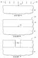
- FIG. 1is a diagrammatic, cross-sectional, fragmentary view of a semiconductor substrate in process in accordance with an aspect of the invention.
- FIG. 2is a view of the FIG. 1 substrate fragment at a processing step subsequent to that shown by FIG. 1 .
- FIG. 3is a view of the FIG. 2 substrate fragment at a processing step subsequent to that shown by FIG. 2 .
- FIG. 4is a diagrammatic, cross-sectional, fragmentary view of a prior art semiconductor substrate processed in contrast to the FIG. 3 substrate fragment.
- FIG. 5is a diagrammatic, cross-sectional, fragmentary view of a semiconductor substrate in process in accordance with an aspect of the invention.
- FIG. 6is a view of the FIG. 5 substrate fragment at a processing step subsequent to that shown by FIG. 5 .
- FIG. 7is a view of the FIG. 6 substrate fragment at a processing step subsequent to that shown by FIG. 6 .
- a wafer fragment 10comprises a semiconductor substrate 12 .
- semiconductor substrateor “semiconductive substrate” is defined to mean any construction comprising semiconductive material, including, but not limited to, bulk semiconductive materials such as a semiconductive wafer (either alone or in assemblies comprising other materials thereon), and semiconductive material layers (either alone or in assemblies comprising other materials).
- substraterefers to any supporting structure, including, but not limited to, the semiconductive substrates described above.
- the term “layer”encompasses the singular and the plural unless otherwise indicated. Accordingly, semiconductor substrate 12 might comprise multiple different materials and/or layers which may include, by way of example only, bulk semiconductor materials and/or semiconductor-on-insulator layers.
- Antireflective coating 14is deposited over semiconductor substrate 12 .
- Antireflective coating 14has an outer surface 16 .
- Outer surface 16could be organic, alternately inorganic, or a combination of organic and inorganic.
- Exemplary inorganic materialsinclude various DARC materials as described above.
- Exemplary organic materialsinclude the above-described BARCs. The invention was reduced to practice utilizing DongJin A20 BARC available from the DongJin Semiconductor Company, Ltd. of Kyungki-do of South Korea. However, of course, any material for outer surface 16 is contemplated, whether existing or yet-to-be developed.
- the basic treating fluidmight be liquid, gaseous, or a combination of liquid and gaseous.
- a basic treating fluidwhich is “liquid” or “gaseous” constitutes at least 95% of such phase.
- the basic treating fluidhas a pH of at least 8.5, and more preferably a pH of at least 10.5.
- exemplary preferred basic treating fluidsinclude tetramethyl ammonium hydroxide, potassium hydroxide, sodium hydroxide, ammonium fluoride, and aqueous alkylamine fluids.
- Specific exemplary alkyl aminesinclude ethylamine, cyclohexylamine, and methylbutylamine.
- various combinations or mixtures of the stated, or other materialsmight also be employed.
- the treatingmight be conducted under room ambient temperature and room ambient pressure conditions with the basic treating fluid thereat, although temperatures and/or pressures above and/or below room ambient conditions are also of course contemplated. Accordingly, any combination of pressure and temperature might be employed. Any time of treating can be employed, with 2 minutes or less being one preferred example, and 1 minute or less being a more preferred example. Such might be dependent upon pH, treatment pressure, treatment temperature, etc. in conjunction with being effective to obtain some desired objective from the treating.
- a positive photoresist 18is applied onto outer surface 16 (meaning in contact therewith) which has been treated with the basic treating fluid.
- An exemplary, and reduction to practice materialwas AR360 available from the Shipley Company of Marlborough, Mass. Any desired suitable thicknesses can be utilized for layers 14 and 18 .
- an exemplary thickness range for layer 14is from 300 Angstroms to 800 Angstroms, with an exemplary thickness range for layer 18 being from 2000 Angstroms to 3350 Angstroms.
- positive photoresist 18has been patterned and developed effective to form a patterned photoresist layer 18 a .
- layer 18 acan be considered as having a base region 20 where the depicted footing commences.
- the, outer surface treating with the basic fluidresults in the patterning and developing of the positive photoresist being effective to form the patterned photoresist layer to have increased footing at the base region of said layer than would otherwise occur in the absence of treating the outer surface with a basic fluid.
- FIG. 4depicts a prior art construction identical with the FIG. 3 construction and processed in accordance therewith identically but for treating of outer surface 16 of antireflective coating 14 with a basic fluid.
- FIG. 3depicts greater degree or increased footing than occurred relative to the FIG. 4 processing.
- outer surface 16is at least partially dried intermediate the basic fluid treating and the application of positive photoresist, and even more preferably completely dried intermediate the treating and photoresist applying. Further preferably in one preferred embodiment, outer surface 16 is not exposed to any liquid intermediate the basic fluid treating and the application of positive photoresist. For example, and preferably, outer surface 16 is allowed to dry under ambient or elevated temperature conditions without any intervening spraying or even rinsing with deionized water over outer surface 16 . Alternately but less preferred in an aspect of the invention, the outer surface might be treated with other fluids (for example which may be aqueous, non-aqueous, pH neutral, pH below 7, gaseous, liquid, etc.) intermediate the basic fluid treating and the application of photoresist.
- other fluidsfor example which may be aqueous, non-aqueous, pH neutral, pH below 7, gaseous, liquid, etc.
- outer surface 16might be treated multiple discrete times with the same or different basic fluids.
- treatment of a surface with a basic fluid prior to photoresist application in accordance with the inventionmight be for any purpose, including for yet to-be-determined purposes, reasons or objectives.
- An existing purposemight be to consume known or unknown reactants present on the surface being treated which might otherwise adversely affect same aspect of the subsequent photoresist processing.
- the inventionwas reduced to practice, for example, in conjunction with inventive processing depicted by FIG. 3 relative to a series of control wafers depicted in FIG. 4 .
- the control and inventive waferswere identically processed, but for treatment with a basic fluid to outer surface 16 prior to application of a photoresist layer thereover.
- the antireflective coating material utilizedwas the DongJin A20 BARC, with the photoresist being AR360 positive Shipley photoresist.
- the basic fluid utilizedwas liquid tetramethyl ammonium hydroxide having a pH of 10.9. Such was puddled atop outer surface 16 , with the basic fluid and substrate being at room ambient temperature and pressure conditions.
- the substrateswere spun to substantially expel the liquid from outer surface 16 . Such outer surface was then allowed to completely dry in an amine scavenging ambient prior to application of the Shipley A360 photoresist.
- the widths of the masking blockswere measured at multiple elevations for determining ratios of a width at the middle illustrated portions of the masking blocks of FIGS. 3 and 4 as compared to the widest portions at the feet of such masking blocks.
- the control wafers as depicted in FIG. 4provided an average ratio of foot width to middle width of 1.504, whereas the substrates processed in accordance with the invention had an average ratio of foot width to middle width of 2.060, thereby demonstrating increased degree of footing.
- Treatment with the basic fluidmight enhance adhesion of the photoresist to an antireflective coating, and/or increased footing can result in a greater area of adhesion to an antireflective coating which might be significant in preventing masking blocks with large aspect ratios from toppling.
- the inventionwas principally developed and directed to the issues and substrate constructions for example as generally described above.
- the inventionis in no way so limited and may have applicability in other aspects and implementations.
- processingmight occur as described above utilizing an antireflective coating with a basic fluid treatment and independent of whether increased footing occurs as compared to non-basic fluid treated antireflective coating surfaces.
- the inventionis applicable to treatment of substrates which do not necessarily have antireflective coatings, and accordingly, might even be highly reflective or transmissive of the incident radiation utilized to pattern the photoresist.
- the treated outer surfacesmight comprise silicon oxide materials, for example, boron and/or phosphorous doped silicon dioxide glasses.
- the treated outer surfacesmight comprise a nitride, such as silicon nitride or titanium nitride.
- the outer surfacemight comprise a material such as silicon carbide which has previously been used as a hard masking material in multilayer resist systems.
- FIGS. 5-7depict an implementation and a method of forming a patterned photoresist layer over a semiconductor substrate in accordance with an aspect of the invention.
- a semiconductor substrate 30has an outer surface 32 .
- Suchmight comprise an antireflective material, a highly reflective material, or a light transmissive material relative to incident radiation ultimately to be utilized in fabricating a photoresist layer.
- semiconductor substrate 30comprises material 34 which may constitute one or more layer or layers of insulative, conductive, and/or semiconductive materials which might be homogenously or non-homogenously distributed.
- outer surface 32is treated with a basic fluid as depicted by downwardly directed arrows 36 .
- the basic fluid treatingis preferably in accordance with any of the attributes described above with respect to the first embodiment, and as claimed herein.
- photoresist 38has been applied onto outer surface 32 which has previously been treated with the basic treating fluid. Attributes are preferably as described above, and as claimed herein. Again, reflective, antireflective, or radiation transmissive materials might be utilized above or below layer 38 , and layer 38 might constitute one or a combination of positive and/or negative photoresists, as well as other layers which might not be radiation sensitive.
- photoresist 38has been patterned and developed to form a patterned photoresist layer 38 a . Etching of material beneath layer 38 a , or ion implanting or other processing whether existing or yet-to-be developed, could then be conducted through openings formed in layer 38 a.
Landscapes
- Engineering & Computer Science (AREA)
- Physics & Mathematics (AREA)
- General Physics & Mathematics (AREA)
- Condensed Matter Physics & Semiconductors (AREA)
- Manufacturing & Machinery (AREA)
- Computer Hardware Design (AREA)
- Microelectronics & Electronic Packaging (AREA)
- Power Engineering (AREA)
- Architecture (AREA)
- Structural Engineering (AREA)
- Exposure Of Semiconductors, Excluding Electron Or Ion Beam Exposure (AREA)
- Photosensitive Polymer And Photoresist Processing (AREA)
Abstract
Description
- This invention relates to methods of forming patterned photoresist layers over semiconductor substrates.
- A continuing goal in semiconductor processing is increased miniaturization while maintaining high performance. Modern semiconductor processes are still heavily reliant on photolithography when fabricating semiconductor circuitry to achieve this goal.
- Photolithography is a commonly-used method for patterning features during semiconductor processing. A radiation-sensitive material (i.e., photoresist) is formed over a substrate which is ultimately to be patterned, for example by etching or ion implanting. The photoresist is subsequently subjected to radiation which modifies the solubility of the impacted versus the unimpacted regions in a suitable developer solution. Accordingly, the radiation is provided in a desired pattern so that some portions of the photoresist are impacted by the radiation while other portions of the photoresist are not impacted by the radiation. The photoresist is then subjected to developing conditions which selectively remove either the impacted or the non-impacted portions. Photoresists are typically designed to be either negative or positive. If the photoresist is a positive photoresist, the impacted portions are selectively removed. If the photoresist is a negative photoresist, the non-impacted portions are selectively removed.
- The photoresist remaining after development defines a patterned mask. The pattern of such mask can subsequently be transferred to the underlying material using appropriate etching and/or implanting techniques to form patterned features in material beneath the mask. A difficulty which can be encountered during photolithographic processing is that the radiation utilized to pattern the photoresist can be reflected from the underlying layer or layers to cause various constructive and destructive interference patterns to occur. This can adversely affect the pattern ultimately developed in the photoresist.
- One manner of addressing the reflective issues is to initially form an antireflective coating over the layer or layers to be patterned, and forming a layer of photoresist thereover. Further, multiple antireflective coating materials or layers might be utilized, as well as multiple layers of resist and/or non-radiation sensitive hard masking or other layers. Various antireflective coating materials have been developed. Some are principally organic in nature, while others are principally inorganic in nature. DARC, which stands for Deposited Antireflective Coating, is typically understood within the industry to define inorganic antireflective coatings formed of silicon, oxygen, nitrogen and sometimes hydrogen. Another commonly used class of antireflective coating is BARC, which stands for Bottom Antireflective Coating. BARC materials are principally organic in nature.
- The continuing goal and effect of circuitry miniaturization has typically resulted in greater reduction in the horizontal dimension as opposed to the vertical dimension. In the etching of features, this has resulted in narrower yet correspondingly increasing height in the features being formed, something typically referred to as increasing aspect ratio. Correspondingly, the photoresist masks utilized to form such features typically also have increased aspect ratios. Accordingly, adherence of the photoresist to the underlying antireflective coating or other layers takes on increasing significance towards precluding displacement or toppling of the masking blocks formed in the patterned photoresist. Further and regardless, the photoresist and antireflective coating materials can interact, particularly during a post-exposure bake of the photoresist prior to solvent development. For example, material at the outer surface of the antireflective coating materials can migrate into the photoresist, and/or the photoresist can interact with material on the outer surface of the antireflective coating which can, one or both, adversely affect adherence or desired control in the ultimate pattern produced in the photoresist.
- In most instances, it is highly desirable that the photoresist masking blocks which are formed have substantially vertical sidewalls from top to bottom of the photoresist layer. However, the patterned photoresist can tend to flare out at the bottom/bases of the individual masking blocks forming what is commonly referred to as footing. The degree of footing can be exacerbated by use of certain antireflective coatings, principally the result of interaction between the photoresist and outer surface of the antireflective coating.
- While the invention was motivated in addressing the above-identified issues, it is in no way so limited. The invention is only limited by the accompanying claims as literally worded, without interpretative or other limiting reference to the specification, and in accordance with the doctrine of equivalents.
- This invention comprises methods of forming patterned photoresist layers over semiconductor substrates. In one implementation, a semiconductor substrate is provided. An antireflective coating is formed over the semiconductor substrate. The antireflective coating has an outer surface. The outer surface is treated with a basic fluid. A positive photoresist is applied onto the outer surface which has been treated with the basic treating fluid. The positive photoresist is patterned and developed effective to form a patterned photoresist layer having increased footing at a base region of said layer than would otherwise occur in the absence of said treating the outer surface.
- In one implementation, a method of forming a patterned photoresist layer over a semiconductor substrate includes providing a semiconductor substrate having an outer surface. The outer surface is treated with a basic fluid. Photoresist is applied onto the outer surface which has been treated with the basic treating fluid. The photoresist is patterned and developed to form a patterned photoresist layer.
- Other aspects and implementations are contemplated.
- Preferred embodiments of the invention are described below with reference to the following accompanying drawings.
FIG. 1 is a diagrammatic, cross-sectional, fragmentary view of a semiconductor substrate in process in accordance with an aspect of the invention.FIG. 2 is a view of theFIG. 1 substrate fragment at a processing step subsequent to that shown byFIG. 1 .FIG. 3 is a view of theFIG. 2 substrate fragment at a processing step subsequent to that shown byFIG. 2 .FIG. 4 is a diagrammatic, cross-sectional, fragmentary view of a prior art semiconductor substrate processed in contrast to theFIG. 3 substrate fragment.FIG. 5 is a diagrammatic, cross-sectional, fragmentary view of a semiconductor substrate in process in accordance with an aspect of the invention.FIG. 6 is a view of theFIG. 5 substrate fragment at a processing step subsequent to that shown byFIG. 5 .FIG. 7 is a view of theFIG. 6 substrate fragment at a processing step subsequent to that shown byFIG. 6 .- This disclosure of the invention is submitted in furtherance of the constitutional purposes of the U.S. Patent Laws “to promote the progress of science and useful arts” (Article 1, Section 8).
- A method of forming a patterned photoresist layer over a semiconductor substrate is described initially with reference to an exemplary embodiment as depicted in
FIGS. 1-3 . Referring initially toFIG. 1 , awafer fragment 10 comprises asemiconductor substrate 12. In the context of this document, the term “semiconductor substrate” or “semiconductive substrate” is defined to mean any construction comprising semiconductive material, including, but not limited to, bulk semiconductive materials such as a semiconductive wafer (either alone or in assemblies comprising other materials thereon), and semiconductive material layers (either alone or in assemblies comprising other materials). The term “substrate” refers to any supporting structure, including, but not limited to, the semiconductive substrates described above. Further, the term “layer” encompasses the singular and the plural unless otherwise indicated. Accordingly,semiconductor substrate 12 might comprise multiple different materials and/or layers which may include, by way of example only, bulk semiconductor materials and/or semiconductor-on-insulator layers. - An,
antireflective coating 14 is deposited oversemiconductor substrate 12.Antireflective coating 14 has anouter surface 16.Outer surface 16 could be organic, alternately inorganic, or a combination of organic and inorganic. Exemplary inorganic materials, and by way of example only, include various DARC materials as described above. Exemplary organic materials include the above-described BARCs. The invention was reduced to practice utilizing DongJin A20 BARC available from the DongJin Semiconductor Company, Ltd. of Kyungki-do of South Korea. However, of course, any material forouter surface 16 is contemplated, whether existing or yet-to-be developed. Outer surface 16 is treated with a basic fluid exemplified by the depicted downwardly directedarrows 18. The basic treating fluid might be liquid, gaseous, or a combination of liquid and gaseous. In the context of this document, a basic treating fluid which is “liquid” or “gaseous” constitutes at least 95% of such phase. Regardless, in one preferred implementation, the basic treating fluid has a pH of at least 8.5, and more preferably a pH of at least 10.5. By way of example only, exemplary preferred basic treating fluids include tetramethyl ammonium hydroxide, potassium hydroxide, sodium hydroxide, ammonium fluoride, and aqueous alkylamine fluids. Specific exemplary alkyl amines include ethylamine, cyclohexylamine, and methylbutylamine. Of course, various combinations or mixtures of the stated, or other materials, might also be employed.- The treating might be conducted under room ambient temperature and room ambient pressure conditions with the basic treating fluid thereat, although temperatures and/or pressures above and/or below room ambient conditions are also of course contemplated. Accordingly, any combination of pressure and temperature might be employed. Any time of treating can be employed, with 2 minutes or less being one preferred example, and 1 minute or less being a more preferred example. Such might be dependent upon pH, treatment pressure, treatment temperature, etc. in conjunction with being effective to obtain some desired objective from the treating.
- Referring to
FIG. 2 , apositive photoresist 18 is applied onto outer surface16 (meaning in contact therewith) which has been treated with the basic treating fluid. An exemplary, and reduction to practice material was AR360 available from the Shipley Company of Marlborough, Mass. Any desired suitable thicknesses can be utilized forlayers layer 14 is from 300 Angstroms to 800 Angstroms, with an exemplary thickness range forlayer 18 being from 2000 Angstroms to 3350 Angstroms. - Referring to
FIG. 3 ,positive photoresist 18 has been patterned and developed effective to form a patternedphotoresist layer 18a. As depicted,layer 18acan be considered as having abase region 20 where the depicted footing commences. In accordance with one aspect of the invention, the, outer surface treating with the basic fluid results in the patterning and developing of the positive photoresist being effective to form the patterned photoresist layer to have increased footing at the base region of said layer than would otherwise occur in the absence of treating the outer surface with a basic fluid. For example,FIG. 4 depicts a prior art construction identical with theFIG. 3 construction and processed in accordance therewith identically but for treating ofouter surface 16 ofantireflective coating 14 with a basic fluid.FIG. 3 depicts greater degree or increased footing than occurred relative to theFIG. 4 processing. - In one preferred implementation,
outer surface 16 is at least partially dried intermediate the basic fluid treating and the application of positive photoresist, and even more preferably completely dried intermediate the treating and photoresist applying. Further preferably in one preferred embodiment,outer surface 16 is not exposed to any liquid intermediate the basic fluid treating and the application of positive photoresist. For example, and preferably,outer surface 16 is allowed to dry under ambient or elevated temperature conditions without any intervening spraying or even rinsing with deionized water overouter surface 16. Alternately but less preferred in an aspect of the invention, the outer surface might be treated with other fluids (for example which may be aqueous, non-aqueous, pH neutral, pH below 7, gaseous, liquid, etc.) intermediate the basic fluid treating and the application of photoresist. Further,outer surface 16 might be treated multiple discrete times with the same or different basic fluids. Regardless, treatment of a surface with a basic fluid prior to photoresist application in accordance with the invention might be for any purpose, including for yet to-be-determined purposes, reasons or objectives. An existing purpose might be to consume known or unknown reactants present on the surface being treated which might otherwise adversely affect same aspect of the subsequent photoresist processing. - The invention was reduced to practice, for example, in conjunction with inventive processing depicted by
FIG. 3 relative to a series of control wafers depicted inFIG. 4 . The control and inventive wafers were identically processed, but for treatment with a basic fluid toouter surface 16 prior to application of a photoresist layer thereover. The antireflective coating material utilized was the DongJin A20 BARC, with the photoresist being AR360 positive Shipley photoresist. The basic fluid utilized was liquid tetramethyl ammonium hydroxide having a pH of 10.9. Such was puddled atopouter surface 16, with the basic fluid and substrate being at room ambient temperature and pressure conditions. After approximately 60 seconds of such treating, the substrates were spun to substantially expel the liquid fromouter surface 16. Such outer surface was then allowed to completely dry in an amine scavenging ambient prior to application of the Shipley A360 photoresist. Upon radiation exposure and develop, the widths of the masking blocks were measured at multiple elevations for determining ratios of a width at the middle illustrated portions of the masking blocks ofFIGS. 3 and 4 as compared to the widest portions at the feet of such masking blocks. The control wafers as depicted inFIG. 4 provided an average ratio of foot width to middle width of 1.504, whereas the substrates processed in accordance with the invention had an average ratio of foot width to middle width of 2.060, thereby demonstrating increased degree of footing. Treatment with the basic fluid might enhance adhesion of the photoresist to an antireflective coating, and/or increased footing can result in a greater area of adhesion to an antireflective coating which might be significant in preventing masking blocks with large aspect ratios from toppling. - The invention was principally developed and directed to the issues and substrate constructions for example as generally described above. However, the invention is in no way so limited and may have applicability in other aspects and implementations. For example, processing might occur as described above utilizing an antireflective coating with a basic fluid treatment and independent of whether increased footing occurs as compared to non-basic fluid treated antireflective coating surfaces. Further by way of example only, the invention is applicable to treatment of substrates which do not necessarily have antireflective coatings, and accordingly, might even be highly reflective or transmissive of the incident radiation utilized to pattern the photoresist. Regardless, by way of example only, the treated outer surfaces might comprise silicon oxide materials, for example, boron and/or phosphorous doped silicon dioxide glasses. Alternately by way of example only, the treated outer surfaces might comprise a nitride, such as silicon nitride or titanium nitride. Further, by way of example only, the outer surface might comprise a material such as silicon carbide which has previously been used as a hard masking material in multilayer resist systems.
- Further and regardless, the invention has applicability to use with negative photoresists in addition to positive photoresists, and regardless of use of an antireflective coating.
FIGS. 5-7 depict an implementation and a method of forming a patterned photoresist layer over a semiconductor substrate in accordance with an aspect of the invention. Referring initially toFIG. 5 , asemiconductor substrate 30 has anouter surface 32. Such might comprise an antireflective material, a highly reflective material, or a light transmissive material relative to incident radiation ultimately to be utilized in fabricating a photoresist layer. Further,semiconductor substrate 30 comprisesmaterial 34 which may constitute one or more layer or layers of insulative, conductive, and/or semiconductive materials which might be homogenously or non-homogenously distributed. Regardless,outer surface 32 is treated with a basic fluid as depicted by downwardly directedarrows 36. The basic fluid treating is preferably in accordance with any of the attributes described above with respect to the first embodiment, and as claimed herein. - Referring to
FIG. 6 ,photoresist 38 has been applied ontoouter surface 32 which has previously been treated with the basic treating fluid. Attributes are preferably as described above, and as claimed herein. Again, reflective, antireflective, or radiation transmissive materials might be utilized above or belowlayer 38, andlayer 38 might constitute one or a combination of positive and/or negative photoresists, as well as other layers which might not be radiation sensitive. - Referring to
FIG. 7 ,photoresist 38 has been patterned and developed to form a patternedphotoresist layer 38a. Etching of material beneathlayer 38a, or ion implanting or other processing whether existing or yet-to-be developed, could then be conducted through openings formed inlayer 38a. - In compliance with the statute, the invention has been described in language more or less specific as to structural and methodical features. It is to be understood, however, that the invention is not limited to the specific features shown and described, since the means wherein disclosed comprise preferred forms of putting the invention into effect. The invention is, therefore, claimed in any of its forms or modifications within the proper scope of the appended claims appropriately interpreted in accordance with the doctrine of equivalents.
Claims (71)
Priority Applications (3)
| Application Number | Priority Date | Filing Date | Title |
|---|---|---|---|
| US10/655,997US7115532B2 (en) | 2003-09-05 | 2003-09-05 | Methods of forming patterned photoresist layers over semiconductor substrates |
| US11/481,493US7985698B2 (en) | 2003-09-05 | 2006-07-05 | Methods of forming patterned photoresist layers over semiconductor substrates |
| US13/163,890US8334221B2 (en) | 2003-09-05 | 2011-06-20 | Methods of forming patterned photoresist layers over semiconductor substrates |
Applications Claiming Priority (1)
| Application Number | Priority Date | Filing Date | Title |
|---|---|---|---|
| US10/655,997US7115532B2 (en) | 2003-09-05 | 2003-09-05 | Methods of forming patterned photoresist layers over semiconductor substrates |
Related Child Applications (1)
| Application Number | Title | Priority Date | Filing Date |
|---|---|---|---|
| US11/481,493ContinuationUS7985698B2 (en) | 2003-09-05 | 2006-07-05 | Methods of forming patterned photoresist layers over semiconductor substrates |
Publications (2)
| Publication Number | Publication Date |
|---|---|
| US20050054216A1true US20050054216A1 (en) | 2005-03-10 |
| US7115532B2 US7115532B2 (en) | 2006-10-03 |
Family
ID=34226255
Family Applications (3)
| Application Number | Title | Priority Date | Filing Date |
|---|---|---|---|
| US10/655,997Expired - Fee RelatedUS7115532B2 (en) | 2003-09-05 | 2003-09-05 | Methods of forming patterned photoresist layers over semiconductor substrates |
| US11/481,493Active2027-01-04US7985698B2 (en) | 2003-09-05 | 2006-07-05 | Methods of forming patterned photoresist layers over semiconductor substrates |
| US13/163,890Expired - Fee RelatedUS8334221B2 (en) | 2003-09-05 | 2011-06-20 | Methods of forming patterned photoresist layers over semiconductor substrates |
Family Applications After (2)
| Application Number | Title | Priority Date | Filing Date |
|---|---|---|---|
| US11/481,493Active2027-01-04US7985698B2 (en) | 2003-09-05 | 2006-07-05 | Methods of forming patterned photoresist layers over semiconductor substrates |
| US13/163,890Expired - Fee RelatedUS8334221B2 (en) | 2003-09-05 | 2011-06-20 | Methods of forming patterned photoresist layers over semiconductor substrates |
Country Status (1)
| Country | Link |
|---|---|
| US (3) | US7115532B2 (en) |
Cited By (9)
| Publication number | Priority date | Publication date | Assignee | Title |
|---|---|---|---|---|
| US20070037089A1 (en)* | 2005-08-09 | 2007-02-15 | Taiwan Semiconductor Manufacturing Company, Ltd. | Structure and method for improving photoresist pattern adhesion |
| US20070298349A1 (en)* | 2006-06-22 | 2007-12-27 | Ruzhi Zhang | Antireflective Coating Compositions Comprising Siloxane Polymer |
| US20080008954A1 (en)* | 2006-06-22 | 2008-01-10 | Abdallah David J | High silicon-content thin film thermosets |
| US20080199789A1 (en)* | 2007-02-20 | 2008-08-21 | David Abdallah | Antireflective Coating Composition Based on Silicon Polymer |
| US20080196626A1 (en)* | 2007-02-20 | 2008-08-21 | Hengpeng Wu | Silicone coating composition |
| US20090162800A1 (en)* | 2007-12-20 | 2009-06-25 | David Abdallah | Process for Imaging a Photoresist Coated over an Antireflective Coating |
| US20090274974A1 (en)* | 2008-04-30 | 2009-11-05 | David Abdallah | Spin-on graded k silicon antireflective coating |
| US20100093969A1 (en)* | 2007-02-26 | 2010-04-15 | Ruzhi Zhang | Process for making siloxane polymers |
| US20140256146A1 (en)* | 2013-03-11 | 2014-09-11 | Taiwan Semiconductor Manufacturing Company, Ltd. | Method and Structure to Improve Process Window for Lithography |
Families Citing this family (7)
| Publication number | Priority date | Publication date | Assignee | Title |
|---|---|---|---|---|
| US7115532B2 (en) | 2003-09-05 | 2006-10-03 | Micron Technolgoy, Inc. | Methods of forming patterned photoresist layers over semiconductor substrates |
| US7119031B2 (en)* | 2004-06-28 | 2006-10-10 | Micron Technology, Inc. | Methods of forming patterned photoresist layers over semiconductor substrates |
| US7241705B2 (en) | 2004-09-01 | 2007-07-10 | Micron Technology, Inc. | Methods of forming conductive contacts to source/drain regions and methods of forming local interconnects |
| EP2121808A1 (en) | 2007-02-27 | 2009-11-25 | AZ Electronic Materials USA Corp. | Silicon-based antifrelective coating compositions |
| US20100291475A1 (en)* | 2009-05-12 | 2010-11-18 | Chenghong Li | Silicone Coating Compositions |
| US8999840B2 (en)* | 2013-07-11 | 2015-04-07 | Samsung Electronics Co., Ltd. | Method of forming fine patterns of semiconductor device |
| US12359313B2 (en)* | 2019-07-31 | 2025-07-15 | Taiwan Semiconductor Manufacturing Company, Ltd. | Deposition apparatus and method of forming metal oxide layer using the same |
Citations (66)
| Publication number | Priority date | Publication date | Assignee | Title |
|---|---|---|---|---|
| US3349474A (en)* | 1963-12-26 | 1967-10-31 | Rca Corp | Semiconductor device |
| US3772101A (en)* | 1972-05-01 | 1973-11-13 | Ibm | Landless plated-through hole photoresist making process |
| US4086074A (en)* | 1976-01-22 | 1978-04-25 | Corning Glass Works | Antireflective layers on phase separated glass |
| US4622735A (en)* | 1980-12-12 | 1986-11-18 | Tokyo Shibaura Denki Kabushiki Kaisha | Method for manufacturing a semiconductor device utilizing self-aligned silicide regions |
| US4683645A (en)* | 1985-06-28 | 1987-08-04 | Northern Telecom Limited | Process of fabricating MOS devices having shallow source and drain junctions |
| US4693910A (en)* | 1984-05-07 | 1987-09-15 | Hoya Corporation | Process for producing porous antireflective coatings |
| US4766090A (en)* | 1986-04-21 | 1988-08-23 | American Telephone And Telegraph Company, At&T Bell Laboratories | Methods for fabricating latchup-preventing CMOS device |
| US5099304A (en)* | 1988-12-08 | 1992-03-24 | Nec Corporation | Semiconductor device with insulating isolation groove |
| US5236865A (en)* | 1991-01-16 | 1993-08-17 | Micron Technology, Inc. | Method for simultaneously forming silicide and effecting dopant activation on a semiconductor wafer |
| US5406123A (en)* | 1992-06-11 | 1995-04-11 | Engineering Research Ctr., North Carolina State Univ. | Single crystal titanium nitride epitaxial on silicon |
| US5444024A (en)* | 1994-06-10 | 1995-08-22 | Advanced Micro Devices, Inc. | Method for low energy implantation of argon to control titanium silicide formation |
| US5470764A (en)* | 1992-05-20 | 1995-11-28 | Mitsubishi Denki Kabushik Kaisha | Method of manufacturing a semiconductor device with hydrogen ion intercepting layer |
| US5470794A (en)* | 1994-02-23 | 1995-11-28 | Advanced Micro Devices | Method for forming a silicide using ion beam mixing |
| US5470784A (en)* | 1977-12-05 | 1995-11-28 | Plasma Physics Corp. | Method of forming semiconducting materials and barriers using a multiple chamber arrangement |
| US5670298A (en)* | 1992-06-17 | 1997-09-23 | Lg Semicon Co., Ltd. | Method of forming a metal pattern in manufacturing a semiconductor device |
| US5677102A (en)* | 1995-03-28 | 1997-10-14 | Tokyo Ohka Kogyo Co., Ltd. | Method for the preparation of photoresist solution |
| US5904517A (en)* | 1998-07-08 | 1999-05-18 | Advanced Micro Devices, Inc. | Ultra thin high K spacer material for use in transistor fabrication |
| US5955244A (en)* | 1996-08-20 | 1999-09-21 | Quantum Corporation | Method for forming photoresist features having reentrant profiles using a basic agent |
| US5998264A (en)* | 1998-03-06 | 1999-12-07 | Wu; Shye-Lin | Method of forming high density flash memories with MIM structure |
| US6013582A (en)* | 1997-12-08 | 2000-01-11 | Applied Materials, Inc. | Method for etching silicon oxynitride and inorganic antireflection coatings |
| US6037239A (en)* | 1997-04-23 | 2000-03-14 | Elantec, Inc. | Method for making a contact structure for a polysilicon filled trench isolation |
| US6096634A (en)* | 1992-01-31 | 2000-08-01 | Stmicroelectronics, Inc. | Method of patterning a submicron semiconductor layer |
| US6130140A (en)* | 1994-07-14 | 2000-10-10 | Micron Technology, Inc. | Method of forming an isolation structure in a semiconductor device |
| US6133116A (en)* | 1998-06-29 | 2000-10-17 | Samsung Electronics Co., Ltd. | Methods of forming trench isolation regions having conductive shields therein |
| US6133105A (en)* | 1999-04-27 | 2000-10-17 | United Microelectronics Corp. | Method of manufacturing borderless contact hole including a silicide layer on source/drain and sidewall of trench isolation structure |
| US6156674A (en)* | 1998-11-25 | 2000-12-05 | Micron Technology, Inc. | Semiconductor processing methods of forming insulative materials |
| US6165834A (en)* | 1998-05-07 | 2000-12-26 | Micron Technology, Inc. | Method of forming capacitors, method of processing dielectric layers, method of forming a DRAM cell |
| US6177235B1 (en)* | 1996-12-27 | 2001-01-23 | France Telecom | Antireflection treatment of reflective surfaces |
| US6180465B1 (en)* | 1998-11-20 | 2001-01-30 | Advanced Micro Devices | Method of making high performance MOSFET with channel scaling mask feature |
| US6188097B1 (en)* | 1997-07-02 | 2001-02-13 | Micron Technology, Inc. | Rough electrode (high surface area) from Ti and TiN |
| US6207485B1 (en)* | 1998-01-05 | 2001-03-27 | Advanced Micro Devices | Integration of high K spacers for dual gate oxide channel fabrication technique |
| US6255035B1 (en)* | 1999-03-17 | 2001-07-03 | Electron Vision Corporation | Method of creating optimal photoresist structures used in the manufacture of metal T-gates for high-speed semiconductor devices |
| US20010006759A1 (en)* | 1998-09-08 | 2001-07-05 | Charles R. Shipley Jr. | Radiation sensitive compositions |
| US6277728B1 (en)* | 1997-06-13 | 2001-08-21 | Micron Technology, Inc. | Multilevel interconnect structure with low-k dielectric and method of fabricating the structure |
| US6277709B1 (en)* | 2000-07-28 | 2001-08-21 | Vanguard International Semiconductor Corp. | Method of forming shallow trench isolation structure |
| US6281100B1 (en)* | 1998-09-03 | 2001-08-28 | Micron Technology, Inc. | Semiconductor processing methods |
| US6291363B1 (en)* | 1999-03-01 | 2001-09-18 | Micron Technology, Inc. | Surface treatment of DARC films to reduce defects in subsequent cap layers |
| US6297527B1 (en)* | 1999-05-12 | 2001-10-02 | Micron Technology, Inc. | Multilayer electrode for ferroelectric and high dielectric constant capacitors |
| US6350560B1 (en)* | 2000-08-07 | 2002-02-26 | Shipley Company, L.L.C. | Rinse composition |
| US6376149B2 (en)* | 1999-05-26 | 2002-04-23 | Yale University | Methods and compositions for imaging acids in chemically amplified photoresists using pH-dependent fluorophores |
| US6380611B1 (en)* | 1998-09-03 | 2002-04-30 | Micron Technology, Inc. | Treatment for film surface to reduce photo footing |
| US6383723B1 (en)* | 1998-08-28 | 2002-05-07 | Micron Technology, Inc. | Method to clean substrate and improve photoresist profile |
| US20020076879A1 (en)* | 2000-11-30 | 2002-06-20 | Jae-Kyu Lee | Integrated circuit devices having trench isolation structures and methods of fabricating the same |
| US6440793B1 (en)* | 2001-01-10 | 2002-08-27 | International Business Machines Corporation | Vertical MOSFET |
| US6465325B2 (en)* | 2001-02-27 | 2002-10-15 | Fairchild Semiconductor Corporation | Process for depositing and planarizing BPSG for dense trench MOSFET application |
| US20020196651A1 (en)* | 2001-06-22 | 2002-12-26 | Rolf Weis | Memory cell layout with double gate vertical array transistor |
| US20030013272A1 (en)* | 2001-07-03 | 2003-01-16 | Hong Soo-Jin | Trench device isolation structure and a method of forming the same |
| US6511896B2 (en)* | 2001-04-06 | 2003-01-28 | Micron Technology, Inc. | Method of etching a substantially amorphous TA2O5 comprising layer |
| US20030045060A1 (en)* | 2001-08-30 | 2003-03-06 | Micron Technology, Inc. | Crystalline or amorphous medium-k gate oxides, Y2O3 and Gd2O3 |
| US20030045078A1 (en)* | 2001-08-30 | 2003-03-06 | Micron Technology, Inc. | Highly reliable amorphous high-K gate oxide ZrO2 |
| US6548854B1 (en)* | 1997-12-22 | 2003-04-15 | Agere Systems Inc. | Compound, high-K, gate and capacitor insulator layer |
| US6582888B1 (en)* | 1997-10-15 | 2003-06-24 | Siemens Aktiengesellschaft | Method for producing organic electroluminescent components |
| US6582861B2 (en)* | 2001-03-16 | 2003-06-24 | Applied Materials, Inc. | Method of reshaping a patterned organic photoresist surface |
| US6613240B2 (en)* | 1999-12-06 | 2003-09-02 | Epion Corporation | Method and apparatus for smoothing thin conductive films by gas cluster ion beam |
| US20030205729A1 (en)* | 2002-03-11 | 2003-11-06 | Cem Basceri | MIM capacitor with metal nitride electrode materials and method of formation |
| US20030213987A1 (en)* | 2002-05-16 | 2003-11-20 | Cem Basceri | MIS capacitor and method of formation |
| US20030219942A1 (en)* | 2002-05-25 | 2003-11-27 | Kyung-In Choi | Methods of forming capacitors and integrated circuit devices including tantalum nitride |
| US20040043228A1 (en)* | 2002-08-29 | 2004-03-04 | Derderian Garo J. | Method and system for binding halide-based contaminants |
| US6720638B2 (en)* | 2002-06-21 | 2004-04-13 | Micron Technology, Inc. | Semiconductor constructions, and methods of forming semiconductor constructions |
| US6780766B2 (en)* | 2001-04-06 | 2004-08-24 | Micron Technology, Inc. | Methods of forming regions of differing composition over a substrate |
| US6817086B2 (en)* | 2001-05-10 | 2004-11-16 | International Business Machines Corporation | Photolithographic process for extreme resolution of track width definition of a read head |
| US20040245560A1 (en)* | 2003-06-03 | 2004-12-09 | Marsela Pontoh | Methods of forming rugged electrically conductive surfaces and layers |
| US6838363B2 (en)* | 2002-09-30 | 2005-01-04 | Advanced Micro Devices, Inc. | Circuit element having a metal silicide region thermally stabilized by a barrier diffusion material |
| US6844131B2 (en)* | 2002-01-09 | 2005-01-18 | Clariant Finance (Bvi) Limited | Positive-working photoimageable bottom antireflective coating |
| US6956980B2 (en)* | 2000-09-18 | 2005-10-18 | Sumitomo Osaka Cement Co., Ltd. | Optical waveguide type optical modulator and production method therefor |
| US20050244571A1 (en)* | 2002-05-21 | 2005-11-03 | Interfloat Corporation | Method and device for the production of an antireflective coating, antireflective coating, and antireflective-coated substrate |
Family Cites Families (11)
| Publication number | Priority date | Publication date | Assignee | Title |
|---|---|---|---|---|
| US5804487A (en)* | 1996-07-10 | 1998-09-08 | Trw Inc. | Method of fabricating high βHBT devices |
| EP0851473A3 (en) | 1996-12-23 | 1998-07-22 | Lucent Technologies Inc. | Method of making a layer with high dielectric K, gate and capacitor insulator layer and device |
| US6096621A (en) | 1997-04-23 | 2000-08-01 | Elantec, Inc. | Polysilicon filled trench isolation structure for soi integrated circuits |
| JP2002323775A (en) | 2001-04-26 | 2002-11-08 | Fujitsu Ltd | Pattern formation method |
| US7384727B2 (en) | 2003-06-26 | 2008-06-10 | Micron Technology, Inc. | Semiconductor processing patterning methods |
| US7115532B2 (en) | 2003-09-05 | 2006-10-03 | Micron Technolgoy, Inc. | Methods of forming patterned photoresist layers over semiconductor substrates |
| US6969677B2 (en)* | 2003-10-20 | 2005-11-29 | Micron Technology, Inc. | Methods of forming conductive metal silicides by reaction of metal with silicon |
| US7026243B2 (en) | 2003-10-20 | 2006-04-11 | Micron Technology, Inc. | Methods of forming conductive material silicides by reaction of metal with silicon |
| US7153769B2 (en) | 2004-04-08 | 2006-12-26 | Micron Technology, Inc. | Methods of forming a reaction product and methods of forming a conductive metal silicide by reaction of metal with silicon |
| US7119031B2 (en) | 2004-06-28 | 2006-10-10 | Micron Technology, Inc. | Methods of forming patterned photoresist layers over semiconductor substrates |
| US7241705B2 (en) | 2004-09-01 | 2007-07-10 | Micron Technology, Inc. | Methods of forming conductive contacts to source/drain regions and methods of forming local interconnects |
- 2003
- 2003-09-05USUS10/655,997patent/US7115532B2/ennot_activeExpired - Fee Related
- 2006
- 2006-07-05USUS11/481,493patent/US7985698B2/enactiveActive
- 2011
- 2011-06-20USUS13/163,890patent/US8334221B2/ennot_activeExpired - Fee Related
Patent Citations (79)
| Publication number | Priority date | Publication date | Assignee | Title |
|---|---|---|---|---|
| US3349474A (en)* | 1963-12-26 | 1967-10-31 | Rca Corp | Semiconductor device |
| US3772101A (en)* | 1972-05-01 | 1973-11-13 | Ibm | Landless plated-through hole photoresist making process |
| US4086074A (en)* | 1976-01-22 | 1978-04-25 | Corning Glass Works | Antireflective layers on phase separated glass |
| US5470784A (en)* | 1977-12-05 | 1995-11-28 | Plasma Physics Corp. | Method of forming semiconducting materials and barriers using a multiple chamber arrangement |
| US4622735A (en)* | 1980-12-12 | 1986-11-18 | Tokyo Shibaura Denki Kabushiki Kaisha | Method for manufacturing a semiconductor device utilizing self-aligned silicide regions |
| US4693910A (en)* | 1984-05-07 | 1987-09-15 | Hoya Corporation | Process for producing porous antireflective coatings |
| US4683645A (en)* | 1985-06-28 | 1987-08-04 | Northern Telecom Limited | Process of fabricating MOS devices having shallow source and drain junctions |
| US4766090A (en)* | 1986-04-21 | 1988-08-23 | American Telephone And Telegraph Company, At&T Bell Laboratories | Methods for fabricating latchup-preventing CMOS device |
| US5099304A (en)* | 1988-12-08 | 1992-03-24 | Nec Corporation | Semiconductor device with insulating isolation groove |
| US5236865A (en)* | 1991-01-16 | 1993-08-17 | Micron Technology, Inc. | Method for simultaneously forming silicide and effecting dopant activation on a semiconductor wafer |
| US6096634A (en)* | 1992-01-31 | 2000-08-01 | Stmicroelectronics, Inc. | Method of patterning a submicron semiconductor layer |
| US5470764A (en)* | 1992-05-20 | 1995-11-28 | Mitsubishi Denki Kabushik Kaisha | Method of manufacturing a semiconductor device with hydrogen ion intercepting layer |
| US5406123A (en)* | 1992-06-11 | 1995-04-11 | Engineering Research Ctr., North Carolina State Univ. | Single crystal titanium nitride epitaxial on silicon |
| US5670298A (en)* | 1992-06-17 | 1997-09-23 | Lg Semicon Co., Ltd. | Method of forming a metal pattern in manufacturing a semiconductor device |
| US5470794A (en)* | 1994-02-23 | 1995-11-28 | Advanced Micro Devices | Method for forming a silicide using ion beam mixing |
| US5444024A (en)* | 1994-06-10 | 1995-08-22 | Advanced Micro Devices, Inc. | Method for low energy implantation of argon to control titanium silicide formation |
| US6130140A (en)* | 1994-07-14 | 2000-10-10 | Micron Technology, Inc. | Method of forming an isolation structure in a semiconductor device |
| US5677102A (en)* | 1995-03-28 | 1997-10-14 | Tokyo Ohka Kogyo Co., Ltd. | Method for the preparation of photoresist solution |
| US5955244A (en)* | 1996-08-20 | 1999-09-21 | Quantum Corporation | Method for forming photoresist features having reentrant profiles using a basic agent |
| US6177235B1 (en)* | 1996-12-27 | 2001-01-23 | France Telecom | Antireflection treatment of reflective surfaces |
| US6037239A (en)* | 1997-04-23 | 2000-03-14 | Elantec, Inc. | Method for making a contact structure for a polysilicon filled trench isolation |
| US6277728B1 (en)* | 1997-06-13 | 2001-08-21 | Micron Technology, Inc. | Multilevel interconnect structure with low-k dielectric and method of fabricating the structure |
| US6238994B1 (en)* | 1997-07-02 | 2001-05-29 | Micron Technology, Inc. | Method of creating a rough electrode (high surface area) from Ti and TiN and resulting article |
| US6608343B2 (en)* | 1997-07-02 | 2003-08-19 | Micron Technology, Inc. | Rough (high surface area) electrode from Ti and TiN, capacitors and semiconductor devices including same |
| US6399982B1 (en)* | 1997-07-02 | 2002-06-04 | Micron Technology, Inc. | Rough (high surface area) electrode from Ti and TiN capacitors and semiconductor devices including same |
| US6188097B1 (en)* | 1997-07-02 | 2001-02-13 | Micron Technology, Inc. | Rough electrode (high surface area) from Ti and TiN |
| US6582888B1 (en)* | 1997-10-15 | 2003-06-24 | Siemens Aktiengesellschaft | Method for producing organic electroluminescent components |
| US6013582A (en)* | 1997-12-08 | 2000-01-11 | Applied Materials, Inc. | Method for etching silicon oxynitride and inorganic antireflection coatings |
| US6548854B1 (en)* | 1997-12-22 | 2003-04-15 | Agere Systems Inc. | Compound, high-K, gate and capacitor insulator layer |
| US6207485B1 (en)* | 1998-01-05 | 2001-03-27 | Advanced Micro Devices | Integration of high K spacers for dual gate oxide channel fabrication technique |
| US5998264A (en)* | 1998-03-06 | 1999-12-07 | Wu; Shye-Lin | Method of forming high density flash memories with MIM structure |
| US6165834A (en)* | 1998-05-07 | 2000-12-26 | Micron Technology, Inc. | Method of forming capacitors, method of processing dielectric layers, method of forming a DRAM cell |
| US6133116A (en)* | 1998-06-29 | 2000-10-17 | Samsung Electronics Co., Ltd. | Methods of forming trench isolation regions having conductive shields therein |
| US5904517A (en)* | 1998-07-08 | 1999-05-18 | Advanced Micro Devices, Inc. | Ultra thin high K spacer material for use in transistor fabrication |
| US6383723B1 (en)* | 1998-08-28 | 2002-05-07 | Micron Technology, Inc. | Method to clean substrate and improve photoresist profile |
| US6281100B1 (en)* | 1998-09-03 | 2001-08-28 | Micron Technology, Inc. | Semiconductor processing methods |
| US6380611B1 (en)* | 1998-09-03 | 2002-04-30 | Micron Technology, Inc. | Treatment for film surface to reduce photo footing |
| US20010006759A1 (en)* | 1998-09-08 | 2001-07-05 | Charles R. Shipley Jr. | Radiation sensitive compositions |
| US6180465B1 (en)* | 1998-11-20 | 2001-01-30 | Advanced Micro Devices | Method of making high performance MOSFET with channel scaling mask feature |
| US6156674A (en)* | 1998-11-25 | 2000-12-05 | Micron Technology, Inc. | Semiconductor processing methods of forming insulative materials |
| US6291363B1 (en)* | 1999-03-01 | 2001-09-18 | Micron Technology, Inc. | Surface treatment of DARC films to reduce defects in subsequent cap layers |
| US6255035B1 (en)* | 1999-03-17 | 2001-07-03 | Electron Vision Corporation | Method of creating optimal photoresist structures used in the manufacture of metal T-gates for high-speed semiconductor devices |
| US6133105A (en)* | 1999-04-27 | 2000-10-17 | United Microelectronics Corp. | Method of manufacturing borderless contact hole including a silicide layer on source/drain and sidewall of trench isolation structure |
| US6297527B1 (en)* | 1999-05-12 | 2001-10-02 | Micron Technology, Inc. | Multilayer electrode for ferroelectric and high dielectric constant capacitors |
| US6744093B2 (en)* | 1999-05-12 | 2004-06-01 | Micron Technology, Inc. | Multilayer electrode for a ferroelectric capacitor |
| US6900497B2 (en)* | 1999-05-12 | 2005-05-31 | Micron Technology, Inc. | Integrated circuit with a capacitor comprising an electrode |
| US6777739B2 (en)* | 1999-05-12 | 2004-08-17 | Micron Technology, Inc. | Multilayer electrode for a ferroelectric capacitor |
| US6746916B2 (en)* | 1999-05-12 | 2004-06-08 | Micron Technology, Inc. | Method for forming a multilayer electrode for a ferroelectric capacitor |
| US6376149B2 (en)* | 1999-05-26 | 2002-04-23 | Yale University | Methods and compositions for imaging acids in chemically amplified photoresists using pH-dependent fluorophores |
| US6613240B2 (en)* | 1999-12-06 | 2003-09-02 | Epion Corporation | Method and apparatus for smoothing thin conductive films by gas cluster ion beam |
| US6277709B1 (en)* | 2000-07-28 | 2001-08-21 | Vanguard International Semiconductor Corp. | Method of forming shallow trench isolation structure |
| US6350560B1 (en)* | 2000-08-07 | 2002-02-26 | Shipley Company, L.L.C. | Rinse composition |
| US6956980B2 (en)* | 2000-09-18 | 2005-10-18 | Sumitomo Osaka Cement Co., Ltd. | Optical waveguide type optical modulator and production method therefor |
| US20020076879A1 (en)* | 2000-11-30 | 2002-06-20 | Jae-Kyu Lee | Integrated circuit devices having trench isolation structures and methods of fabricating the same |
| US6440793B1 (en)* | 2001-01-10 | 2002-08-27 | International Business Machines Corporation | Vertical MOSFET |
| US6465325B2 (en)* | 2001-02-27 | 2002-10-15 | Fairchild Semiconductor Corporation | Process for depositing and planarizing BPSG for dense trench MOSFET application |
| US6582861B2 (en)* | 2001-03-16 | 2003-06-24 | Applied Materials, Inc. | Method of reshaping a patterned organic photoresist surface |
| US6780766B2 (en)* | 2001-04-06 | 2004-08-24 | Micron Technology, Inc. | Methods of forming regions of differing composition over a substrate |
| US6511896B2 (en)* | 2001-04-06 | 2003-01-28 | Micron Technology, Inc. | Method of etching a substantially amorphous TA2O5 comprising layer |
| US6649466B2 (en)* | 2001-04-06 | 2003-11-18 | Micron Technology, Inc. | Method of forming DRAM circuitry |
| US6617250B2 (en)* | 2001-04-06 | 2003-09-09 | Micron Technology, Inc. | Methods of depositing a layer comprising tungsten and methods of forming a transistor gate line |
| US6817086B2 (en)* | 2001-05-10 | 2004-11-16 | International Business Machines Corporation | Photolithographic process for extreme resolution of track width definition of a read head |
| US20020196651A1 (en)* | 2001-06-22 | 2002-12-26 | Rolf Weis | Memory cell layout with double gate vertical array transistor |
| US20030013272A1 (en)* | 2001-07-03 | 2003-01-16 | Hong Soo-Jin | Trench device isolation structure and a method of forming the same |
| US20030045060A1 (en)* | 2001-08-30 | 2003-03-06 | Micron Technology, Inc. | Crystalline or amorphous medium-k gate oxides, Y2O3 and Gd2O3 |
| US20030045078A1 (en)* | 2001-08-30 | 2003-03-06 | Micron Technology, Inc. | Highly reliable amorphous high-K gate oxide ZrO2 |
| US6844131B2 (en)* | 2002-01-09 | 2005-01-18 | Clariant Finance (Bvi) Limited | Positive-working photoimageable bottom antireflective coating |
| US20030205729A1 (en)* | 2002-03-11 | 2003-11-06 | Cem Basceri | MIM capacitor with metal nitride electrode materials and method of formation |
| US6753618B2 (en)* | 2002-03-11 | 2004-06-22 | Micron Technology, Inc. | MIM capacitor with metal nitride electrode materials and method of formation |
| US20040046197A1 (en)* | 2002-05-16 | 2004-03-11 | Cem Basceri | MIS capacitor and method of formation |
| US20030213987A1 (en)* | 2002-05-16 | 2003-11-20 | Cem Basceri | MIS capacitor and method of formation |
| US20050244571A1 (en)* | 2002-05-21 | 2005-11-03 | Interfloat Corporation | Method and device for the production of an antireflective coating, antireflective coating, and antireflective-coated substrate |
| US20030219942A1 (en)* | 2002-05-25 | 2003-11-27 | Kyung-In Choi | Methods of forming capacitors and integrated circuit devices including tantalum nitride |
| US6780728B2 (en)* | 2002-06-21 | 2004-08-24 | Micron Technology, Inc. | Semiconductor constructions, and methods of forming semiconductor constructions |
| US6720638B2 (en)* | 2002-06-21 | 2004-04-13 | Micron Technology, Inc. | Semiconductor constructions, and methods of forming semiconductor constructions |
| US20040043228A1 (en)* | 2002-08-29 | 2004-03-04 | Derderian Garo J. | Method and system for binding halide-based contaminants |
| US6838363B2 (en)* | 2002-09-30 | 2005-01-04 | Advanced Micro Devices, Inc. | Circuit element having a metal silicide region thermally stabilized by a barrier diffusion material |
| US20040245560A1 (en)* | 2003-06-03 | 2004-12-09 | Marsela Pontoh | Methods of forming rugged electrically conductive surfaces and layers |
| US20040245559A1 (en)* | 2003-06-03 | 2004-12-09 | Marsela Pontoh | Capacitor constructions |
Cited By (15)
| Publication number | Priority date | Publication date | Assignee | Title |
|---|---|---|---|---|
| US20070037089A1 (en)* | 2005-08-09 | 2007-02-15 | Taiwan Semiconductor Manufacturing Company, Ltd. | Structure and method for improving photoresist pattern adhesion |
| US8137895B2 (en)* | 2005-08-09 | 2012-03-20 | Taiwan Semiconductor Manufacturing Company, Ltd. | Structure and method for improving photoresist pattern adhesion |
| US7704670B2 (en) | 2006-06-22 | 2010-04-27 | Az Electronic Materials Usa Corp. | High silicon-content thin film thermosets |
| US20070298349A1 (en)* | 2006-06-22 | 2007-12-27 | Ruzhi Zhang | Antireflective Coating Compositions Comprising Siloxane Polymer |
| US20080008954A1 (en)* | 2006-06-22 | 2008-01-10 | Abdallah David J | High silicon-content thin film thermosets |
| US20080199789A1 (en)* | 2007-02-20 | 2008-08-21 | David Abdallah | Antireflective Coating Composition Based on Silicon Polymer |
| US7736837B2 (en) | 2007-02-20 | 2010-06-15 | Az Electronic Materials Usa Corp. | Antireflective coating composition based on silicon polymer |
| US8026040B2 (en) | 2007-02-20 | 2011-09-27 | Az Electronic Materials Usa Corp. | Silicone coating composition |
| US20080196626A1 (en)* | 2007-02-20 | 2008-08-21 | Hengpeng Wu | Silicone coating composition |
| US20100093969A1 (en)* | 2007-02-26 | 2010-04-15 | Ruzhi Zhang | Process for making siloxane polymers |
| WO2009090474A1 (en)* | 2007-12-20 | 2009-07-23 | Az Electronic Materials Usa Corp. | A process for imaging a photoresist coated over an antireflective coating |
| US20090162800A1 (en)* | 2007-12-20 | 2009-06-25 | David Abdallah | Process for Imaging a Photoresist Coated over an Antireflective Coating |
| US20090274974A1 (en)* | 2008-04-30 | 2009-11-05 | David Abdallah | Spin-on graded k silicon antireflective coating |
| US20140256146A1 (en)* | 2013-03-11 | 2014-09-11 | Taiwan Semiconductor Manufacturing Company, Ltd. | Method and Structure to Improve Process Window for Lithography |
| US9159559B2 (en)* | 2013-03-11 | 2015-10-13 | Taiwan Semiconductor Manufacturing Company, Ltd. | Lithography layer with quenchers to prevent pattern collapse |
Also Published As
| Publication number | Publication date |
|---|---|
| US7115532B2 (en) | 2006-10-03 |
| US20110281434A1 (en) | 2011-11-17 |
| US8334221B2 (en) | 2012-12-18 |
| US20060252277A1 (en) | 2006-11-09 |
| US7985698B2 (en) | 2011-07-26 |
Similar Documents
| Publication | Publication Date | Title |
|---|---|---|
| US8334221B2 (en) | Methods of forming patterned photoresist layers over semiconductor substrates | |
| US20060258809A1 (en) | Over-coating agent for forming fine patterns and a method of forming fine patterns using such agent | |
| US6383723B1 (en) | Method to clean substrate and improve photoresist profile | |
| JP2011065136A5 (en) | ||
| US7235345B2 (en) | Agent for forming coating for narrowing patterns and method for forming fine pattern using the same | |
| US20050175926A1 (en) | Coating forming agent for reducing pattern dimension and method of forming fine pattern therewith | |
| US7189499B2 (en) | Method of forming fine patterns | |
| KR20030076242A (en) | Development defect preventing process and material | |
| US6610616B2 (en) | Method for forming micro-pattern of semiconductor device | |
| US20020187438A1 (en) | Development method for manufacturing semiconductors | |
| US7611825B2 (en) | Photolithography method to prevent photoresist pattern collapse | |
| US8409457B2 (en) | Methods of forming a photoresist-comprising pattern on a substrate | |
| KR100694398B1 (en) | Manufacturing Method of Semiconductor Device | |
| US6686129B2 (en) | Partial photoresist etching | |
| US8163468B2 (en) | Method of reducing photoresist defects during fabrication of a semiconductor device | |
| US20040265746A1 (en) | Semiconductor processing patterning methods and constructions | |
| KR100687858B1 (en) | Patterning method of semiconductor device | |
| KR100752172B1 (en) | How to Form Contact Holes | |
| Nakazawa et al. | Fabrication of 0.1 µm Patterns Using an Alternating Phase Shift Mask in ArF Excimer Laser Lithography | |
| KR100905598B1 (en) | Photoresist Pattern Formation Method | |
| KR19990053211A (en) | How to improve the etching selectivity of photoresist | |
| KR20050120412A (en) | Method for forming fine pattern in semiconductor device using immersion lithography process | |
| KR20050064265A (en) | Method of patterning insulating layer for semiconductor device | |
| JP2004078120A (en) | Method for manufacturing semiconductor device | |
| KR19980048093A (en) | Semiconductor device pattern formation method |
Legal Events
| Date | Code | Title | Description |
|---|---|---|---|
| AS | Assignment | Owner name:MICRON TECHNOLOGY, INC., IDAHO Free format text:ASSIGNMENT OF ASSIGNORS INTEREST;ASSIGNOR:DALEY, JON P.;REEL/FRAME:014483/0152 Effective date:20030825 | |
| FEPP | Fee payment procedure | Free format text:PAYOR NUMBER ASSIGNED (ORIGINAL EVENT CODE: ASPN); ENTITY STATUS OF PATENT OWNER: LARGE ENTITY | |
| CC | Certificate of correction | ||
| FPAY | Fee payment | Year of fee payment:4 | |
| FPAY | Fee payment | Year of fee payment:8 | |
| AS | Assignment | Owner name:U.S. BANK NATIONAL ASSOCIATION, AS COLLATERAL AGENT, CALIFORNIA Free format text:SECURITY INTEREST;ASSIGNOR:MICRON TECHNOLOGY, INC.;REEL/FRAME:038669/0001 Effective date:20160426 Owner name:U.S. BANK NATIONAL ASSOCIATION, AS COLLATERAL AGEN Free format text:SECURITY INTEREST;ASSIGNOR:MICRON TECHNOLOGY, INC.;REEL/FRAME:038669/0001 Effective date:20160426 | |
| AS | Assignment | Owner name:MORGAN STANLEY SENIOR FUNDING, INC., AS COLLATERAL AGENT, MARYLAND Free format text:PATENT SECURITY AGREEMENT;ASSIGNOR:MICRON TECHNOLOGY, INC.;REEL/FRAME:038954/0001 Effective date:20160426 Owner name:MORGAN STANLEY SENIOR FUNDING, INC., AS COLLATERAL Free format text:PATENT SECURITY AGREEMENT;ASSIGNOR:MICRON TECHNOLOGY, INC.;REEL/FRAME:038954/0001 Effective date:20160426 | |
| AS | Assignment | Owner name:U.S. BANK NATIONAL ASSOCIATION, AS COLLATERAL AGENT, CALIFORNIA Free format text:CORRECTIVE ASSIGNMENT TO CORRECT THE REPLACE ERRONEOUSLY FILED PATENT #7358718 WITH THE CORRECT PATENT #7358178 PREVIOUSLY RECORDED ON REEL 038669 FRAME 0001. ASSIGNOR(S) HEREBY CONFIRMS THE SECURITY INTEREST;ASSIGNOR:MICRON TECHNOLOGY, INC.;REEL/FRAME:043079/0001 Effective date:20160426 Owner name:U.S. BANK NATIONAL ASSOCIATION, AS COLLATERAL AGEN Free format text:CORRECTIVE ASSIGNMENT TO CORRECT THE REPLACE ERRONEOUSLY FILED PATENT #7358718 WITH THE CORRECT PATENT #7358178 PREVIOUSLY RECORDED ON REEL 038669 FRAME 0001. ASSIGNOR(S) HEREBY CONFIRMS THE SECURITY INTEREST;ASSIGNOR:MICRON TECHNOLOGY, INC.;REEL/FRAME:043079/0001 Effective date:20160426 | |
| FEPP | Fee payment procedure | Free format text:MAINTENANCE FEE REMINDER MAILED (ORIGINAL EVENT CODE: REM.) | |
| AS | Assignment | Owner name:MICRON TECHNOLOGY, INC., IDAHO Free format text:RELEASE BY SECURED PARTY;ASSIGNOR:U.S. BANK NATIONAL ASSOCIATION, AS COLLATERAL AGENT;REEL/FRAME:047243/0001 Effective date:20180629 | |
| LAPS | Lapse for failure to pay maintenance fees | Free format text:PATENT EXPIRED FOR FAILURE TO PAY MAINTENANCE FEES (ORIGINAL EVENT CODE: EXP.); ENTITY STATUS OF PATENT OWNER: LARGE ENTITY | |
| STCH | Information on status: patent discontinuation | Free format text:PATENT EXPIRED DUE TO NONPAYMENT OF MAINTENANCE FEES UNDER 37 CFR 1.362 | |
| FP | Lapsed due to failure to pay maintenance fee | Effective date:20181003 | |
| AS | Assignment | Owner name:MICRON TECHNOLOGY, INC., IDAHO Free format text:RELEASE BY SECURED PARTY;ASSIGNOR:MORGAN STANLEY SENIOR FUNDING, INC., AS COLLATERAL AGENT;REEL/FRAME:050937/0001 Effective date:20190731 |