US20050052745A1 - Optical device and methods of manufacture - Google Patents
Optical device and methods of manufactureDownload PDFInfo
- Publication number
- US20050052745A1 US20050052745A1US10/701,975US70197503AUS2005052745A1US 20050052745 A1US20050052745 A1US 20050052745A1US 70197503 AUS70197503 AUS 70197503AUS 2005052745 A1US2005052745 A1US 2005052745A1
- Authority
- US
- United States
- Prior art keywords
- pixel
- image
- optical device
- optically
- reflective
- Prior art date
- Legal status (The legal status is an assumption and is not a legal conclusion. Google has not performed a legal analysis and makes no representation as to the accuracy of the status listed.)
- Granted
Links
Images


Classifications
- B—PERFORMING OPERATIONS; TRANSPORTING
- B42—BOOKBINDING; ALBUMS; FILES; SPECIAL PRINTED MATTER
- B42D—BOOKS; BOOK COVERS; LOOSE LEAVES; PRINTED MATTER CHARACTERISED BY IDENTIFICATION OR SECURITY FEATURES; PRINTED MATTER OF SPECIAL FORMAT OR STYLE NOT OTHERWISE PROVIDED FOR; DEVICES FOR USE THEREWITH AND NOT OTHERWISE PROVIDED FOR; MOVABLE-STRIP WRITING OR READING APPARATUS
- B42D25/00—Information-bearing cards or sheet-like structures characterised by identification or security features; Manufacture thereof
- B42D25/30—Identification or security features, e.g. for preventing forgery
- B42D25/328—Diffraction gratings; Holograms
- B—PERFORMING OPERATIONS; TRANSPORTING
- B42—BOOKBINDING; ALBUMS; FILES; SPECIAL PRINTED MATTER
- B42D—BOOKS; BOOK COVERS; LOOSE LEAVES; PRINTED MATTER CHARACTERISED BY IDENTIFICATION OR SECURITY FEATURES; PRINTED MATTER OF SPECIAL FORMAT OR STYLE NOT OTHERWISE PROVIDED FOR; DEVICES FOR USE THEREWITH AND NOT OTHERWISE PROVIDED FOR; MOVABLE-STRIP WRITING OR READING APPARATUS
- B42D25/00—Information-bearing cards or sheet-like structures characterised by identification or security features; Manufacture thereof
- B42D25/30—Identification or security features, e.g. for preventing forgery
- B42D25/324—Reliefs
- B—PERFORMING OPERATIONS; TRANSPORTING
- B42—BOOKBINDING; ALBUMS; FILES; SPECIAL PRINTED MATTER
- B42D—BOOKS; BOOK COVERS; LOOSE LEAVES; PRINTED MATTER CHARACTERISED BY IDENTIFICATION OR SECURITY FEATURES; PRINTED MATTER OF SPECIAL FORMAT OR STYLE NOT OTHERWISE PROVIDED FOR; DEVICES FOR USE THEREWITH AND NOT OTHERWISE PROVIDED FOR; MOVABLE-STRIP WRITING OR READING APPARATUS
- B42D25/00—Information-bearing cards or sheet-like structures characterised by identification or security features; Manufacture thereof
- B42D25/30—Identification or security features, e.g. for preventing forgery
- B42D25/36—Identification or security features, e.g. for preventing forgery comprising special materials
- B42D25/373—Metallic materials
- B—PERFORMING OPERATIONS; TRANSPORTING
- B42—BOOKBINDING; ALBUMS; FILES; SPECIAL PRINTED MATTER
- B42D—BOOKS; BOOK COVERS; LOOSE LEAVES; PRINTED MATTER CHARACTERISED BY IDENTIFICATION OR SECURITY FEATURES; PRINTED MATTER OF SPECIAL FORMAT OR STYLE NOT OTHERWISE PROVIDED FOR; DEVICES FOR USE THEREWITH AND NOT OTHERWISE PROVIDED FOR; MOVABLE-STRIP WRITING OR READING APPARATUS
- B42D25/00—Information-bearing cards or sheet-like structures characterised by identification or security features; Manufacture thereof
- B42D25/40—Manufacture
- B42D25/405—Marking
- B42D25/41—Marking using electromagnetic radiation
- B—PERFORMING OPERATIONS; TRANSPORTING
- B42—BOOKBINDING; ALBUMS; FILES; SPECIAL PRINTED MATTER
- B42D—BOOKS; BOOK COVERS; LOOSE LEAVES; PRINTED MATTER CHARACTERISED BY IDENTIFICATION OR SECURITY FEATURES; PRINTED MATTER OF SPECIAL FORMAT OR STYLE NOT OTHERWISE PROVIDED FOR; DEVICES FOR USE THEREWITH AND NOT OTHERWISE PROVIDED FOR; MOVABLE-STRIP WRITING OR READING APPARATUS
- B42D25/00—Information-bearing cards or sheet-like structures characterised by identification or security features; Manufacture thereof
- B42D25/40—Manufacture
- B42D25/405—Marking
- B42D25/425—Marking by deformation, e.g. embossing
- B—PERFORMING OPERATIONS; TRANSPORTING
- B42—BOOKBINDING; ALBUMS; FILES; SPECIAL PRINTED MATTER
- B42D—BOOKS; BOOK COVERS; LOOSE LEAVES; PRINTED MATTER CHARACTERISED BY IDENTIFICATION OR SECURITY FEATURES; PRINTED MATTER OF SPECIAL FORMAT OR STYLE NOT OTHERWISE PROVIDED FOR; DEVICES FOR USE THEREWITH AND NOT OTHERWISE PROVIDED FOR; MOVABLE-STRIP WRITING OR READING APPARATUS
- B42D25/00—Information-bearing cards or sheet-like structures characterised by identification or security features; Manufacture thereof
- B42D25/40—Manufacture
- B42D25/405—Marking
- B42D25/43—Marking by removal of material
- B42D25/44—Marking by removal of material using mechanical means, e.g. engraving
- B—PERFORMING OPERATIONS; TRANSPORTING
- B42—BOOKBINDING; ALBUMS; FILES; SPECIAL PRINTED MATTER
- B42D—BOOKS; BOOK COVERS; LOOSE LEAVES; PRINTED MATTER CHARACTERISED BY IDENTIFICATION OR SECURITY FEATURES; PRINTED MATTER OF SPECIAL FORMAT OR STYLE NOT OTHERWISE PROVIDED FOR; DEVICES FOR USE THEREWITH AND NOT OTHERWISE PROVIDED FOR; MOVABLE-STRIP WRITING OR READING APPARATUS
- B42D25/00—Information-bearing cards or sheet-like structures characterised by identification or security features; Manufacture thereof
- B42D25/40—Manufacture
- B42D25/405—Marking
- B42D25/43—Marking by removal of material
- B42D25/445—Marking by removal of material using chemical means, e.g. etching
- B—PERFORMING OPERATIONS; TRANSPORTING
- B42—BOOKBINDING; ALBUMS; FILES; SPECIAL PRINTED MATTER
- B42D—BOOKS; BOOK COVERS; LOOSE LEAVES; PRINTED MATTER CHARACTERISED BY IDENTIFICATION OR SECURITY FEATURES; PRINTED MATTER OF SPECIAL FORMAT OR STYLE NOT OTHERWISE PROVIDED FOR; DEVICES FOR USE THEREWITH AND NOT OTHERWISE PROVIDED FOR; MOVABLE-STRIP WRITING OR READING APPARATUS
- B42D25/00—Information-bearing cards or sheet-like structures characterised by identification or security features; Manufacture thereof
- B42D25/40—Manufacture
- B42D25/45—Associating two or more layers
- B42D25/465—Associating two or more layers using chemicals or adhesives
- B42D25/47—Associating two or more layers using chemicals or adhesives using adhesives
- B—PERFORMING OPERATIONS; TRANSPORTING
- B44—DECORATIVE ARTS
- B44F—SPECIAL DESIGNS OR PICTURES
- B44F1/00—Designs or pictures characterised by special or unusual light effects
- B44F1/08—Designs or pictures characterised by special or unusual light effects characterised by colour effects
- B44F1/10—Changing, amusing, or secret pictures
- G—PHYSICS
- G02—OPTICS
- G02B—OPTICAL ELEMENTS, SYSTEMS OR APPARATUS
- G02B5/00—Optical elements other than lenses
- G02B5/18—Diffraction gratings
- G02B5/1861—Reflection gratings characterised by their structure, e.g. step profile, contours of substrate or grooves, pitch variations, materials
- G—PHYSICS
- G03—PHOTOGRAPHY; CINEMATOGRAPHY; ANALOGOUS TECHNIQUES USING WAVES OTHER THAN OPTICAL WAVES; ELECTROGRAPHY; HOLOGRAPHY
- G03C—PHOTOSENSITIVE MATERIALS FOR PHOTOGRAPHIC PURPOSES; PHOTOGRAPHIC PROCESSES, e.g. CINE, X-RAY, COLOUR, STEREO-PHOTOGRAPHIC PROCESSES; AUXILIARY PROCESSES IN PHOTOGRAPHY
- G03C8/00—Diffusion transfer processes or agents therefor; Photosensitive materials for such processes
- G03C8/42—Structural details
- G03C8/52—Bases or auxiliary layers; Substances therefor
- G03C8/56—Mordant layers
- B—PERFORMING OPERATIONS; TRANSPORTING
- B41—PRINTING; LINING MACHINES; TYPEWRITERS; STAMPS
- B41M—PRINTING, DUPLICATING, MARKING, OR COPYING PROCESSES; COLOUR PRINTING
- B41M3/00—Printing processes to produce particular kinds of printed work, e.g. patterns
- B41M3/06—Veined printings; Fluorescent printings; Stereoscopic images; Imitated patterns, e.g. tissues, textiles
- B—PERFORMING OPERATIONS; TRANSPORTING
- B41—PRINTING; LINING MACHINES; TYPEWRITERS; STAMPS
- B41M—PRINTING, DUPLICATING, MARKING, OR COPYING PROCESSES; COLOUR PRINTING
- B41M3/00—Printing processes to produce particular kinds of printed work, e.g. patterns
- B41M3/14—Security printing
- B41M3/148—Transitory images, i.e. images only visible from certain viewing angles
- G—PHYSICS
- G03—PHOTOGRAPHY; CINEMATOGRAPHY; ANALOGOUS TECHNIQUES USING WAVES OTHER THAN OPTICAL WAVES; ELECTROGRAPHY; HOLOGRAPHY
- G03H—HOLOGRAPHIC PROCESSES OR APPARATUS
- G03H2224/00—Writing means other than actinic light wave
- G03H2224/02—Mechanical means, e.g. diamond tool
Definitions
- This inventionrelates to an optical device, and in particular to an optical device which, when illuminated by a light source generates one or more images which are observable from particular ranges of viewing angles around the device.
- the devicemay be used in a number of different applications, and it has particular application as an anti-forgery security device on banknotes, credit cards, cheques, share certificates and other valuable documents.
- OTDsoptically variable devices
- EXELGRAMTM deviceused to protect the new series of Hungarian banknotes and American Express US dollar and Euro travellers cheques
- KINEGRAMTM deviceused to protect the current series of German and Swiss banknotes.
- the EXELGRAMTM deviceis described in U.S. Pat. Nos. 5,825,547 and 6,088,161 while the KINEGRAMTM device is described in European patents EP 330,738 and EP 105099.
- the KINEGRAMTM and EXELGRAMTM devicesare examples of foil based diffractive structures that have proven to be highly effective deterrents to the counterfeiting of official documents.
- This class of optically diffractive anti-counterfeiting devicesalso includes the PIXELGRAMTM device that is described in European patent number EP 0 490 923 B1 and U.S. Pat. No. 5,428,479.
- PIXELGRAMTM devicesare manufactured by producing a counterpart diffractive structure wherein the greyness values of each pixel of an optically invariable image are mapped to corresponding small diffractive pixel regions on the PIXELGRAMTM device.
- a more general and useful approach to the design of optically reflecting or diffracting microstructuresis obtained by utilising colour component values (such as the red, green and blue values) of each pixel in the optically invariable image and relating these parameters via a mathematical or computer algorithm to the parameters required to define the geometrical surface shape properties of each small surface region of the three dimensional reflective or diffractive microstructure.
- colour component valuessuch as the red, green and blue values
- a method of manufacturing an optical device which generates an optically variable imagethe image being optically variable in that it varies according to the position of observation, the method including the steps of:
- an optical deviceproviding an optically variable image, corresponding to an optically invariable counterpart image
- the optical deviceincluding a pixellated reflective structure which is an assembly of reflective surface relief pixels and which when illuminated generates the optically variable image, the image being optically variable in that it varies according to the position of observation, wherein each of the reflective surface relief pixels is an individual reflecting surface structure, and wherein the optically variability is produced by differing angular orientations of the individual reflective surface relief pixels.
- an optical deviceproviding an optically variable image, corresponding to an optically invariable counterpart image, including a pixellated reflective or diffractive structure which is an assembly of reflective or diffractive surface relief pixels and which when illuminated generates an optically variable image, the image being optically variable in that it varies when viewed from different observation positions, wherein each of the reflective or diffractive pixels is an individual reflecting or diffracting three-dimensional surface structure which is directly related via a mathematical or computer algorithm to the colour component values of associated pixels of the optically invariable counterpart image.
- a method of printing an optically variable image onto a documentincluding the steps of:
- FIG. 1illustrates an optically invariable image for use in accordance with the present invention.
- FIG. 1Bshows an enlarged detail of FIG. 1 .
- FIG. 2lists the different coloured pixels in the image of FIG. 1 .
- FIG. 3illustrates an example of a micro-surface structure in accordance with an embodiment of the invention.
- FIG. 4illustrates a mask element for generating the structure of FIG. 3 .
- FIG. 5illustrates an optical arrangement for manufacturing optical devices according to an embodiment of the invention.
- FIG. 6illustrates different mask elements for use in accordance with an embodiment of the invention.
- FIG. 7shows examples of microstructure pixel elements according to an embodiment of the invention.
- FIG. 8shows a group of coloured optically invariable pixels matched with microstructure pixel elements according to an embodiment of the invention.
- FIG. 9illustrates artwork being mapped to microstructure pixels in accordance with an embodiment of the invention.
- FIG. 10illustrates artwork being mapped to diffractive microstructure pixels in accordance with another embodiment of the invention.
- FIG. 11shows the palette of diffractive pixels used in FIG. 10 .
- FIG. 12shows an electron or ion beam exposure system for use in an embodiment of the invention.
- FIG. 13shows a mechanical device for use in an embodiment of the invention.
- the present inventionrelates to high security Optically Variable Device (OVD) microstructures and generalised reflecting or diffracting surface structures, particularly for non foil based applications where direct printing into the application substrate or direct reflection or diffraction from the replicated surface structure of the device is a specific requirement.
- OLEDOptically Variable Device
- these new specialised microstructure geometrieshave a particular application related to direct printing onto the document via the use of specialised inks and lacquers.
- the microstructure of the OVDincorporates surface relief variations of relatively large depth dimension (eg 15 to 100 microns).
- ZOROZero Order Reflective Optic
- These multiplexed micro-mirror array devicesuse reflection rather than diffraction as their fundamental OVD mechanism, and a typical OVD microstructure of this type may contain up to one million micro mirror surface regions of dimensions 30 microns ⁇ 30 microns or less with each mirror surface region designed with predetermined angle and curvature properties according to the input picture information.
- the origination of the devicetakes place via a multi-step process using a combination of electron beam lithography, plasma etching or wet chemical etching, photolithography and other specialised processes adopted from the semiconductor industry.
- Particular advantages of such ZORO devicesinclude higher security and lower cost because all steps in the replication process take place within the security printing plant and there is no requirement for an off-line foil production facility.
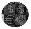
- FIG. 1shows an example of an optically invariable image comprised of multiple picture elements or pixels defined by three colour values denoting the red (R), green (G) and blue (B) components of each pixel.
- RGB colour componentsare used, but it is to be understood that other colour components such as CMYK or HSB are equally usable.
- FIG. 1BAn enlarged detail of FIG. 1 is shown in FIG. 1B .
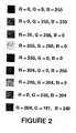
- FIG. 2shows the finite set of independent (R,G,B) values that have been used to construct the image of FIG. 1 .
- This set of (R,G,B) valuesis referred to as the RGB palette of FIG. 1 .
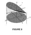
- FIG. 3shows an example of an associated micro-surface structure corresponding to a particular element of a set of (R,G,B) values.
- the micro-surface structurerepresent a micro-reflecting mirror structure and the R, G and B values of each optically invariable pixel determine the surface slope directions and degree of curvature of each of the corresponding micro reflecting mirror structures.
- the micro-surface pixelin this case is 30 microns in diameter.
- FIG. 3shows the micro-surface element itself, and the projection of the element onto the x-y plane.
- FIG. 4shows an example of a colortone mask pixel element that generates the micro-surface relief structure shown in FIG. 3 .
- the edge length of each aperture elementshown by the black squares in FIG.
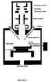
- FIG. 5shows an optical arrangement for manufacturing an optical device according to one aspect of the invention.
- UV lightis allowed to pass through a transparent mask produced by electron beam lithography. After passing through the mask the optical arrangement ensures that the light is then allowed to fall on and expose a surface comprised of photosensitive material, which in this case has a thickness of 30 micron.
- FIG. 6shows an example of a set of transparent pixel elements that can be used as a mask palette to construct a two dimensional mask containing a multiplicity of transparent mask pixels representing the optically invariable image.
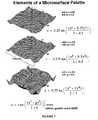
- FIG. 7shows another example of a micro-surface palette function together with computer plots showing three pixel surface elements and their corresponding RGB parameter sets.
- FIG. 8shows a group of seven micro-surface palette elements belonging to the same family shown in FIG. 7 . RGB values and corresponding colour patches are also shown explicitly in FIG. 8 .
- FIG. 9shows the fundamental concept underpinning a key aspect of the invention.
- the same mathematical algorithm used in FIGS. 7 and 8is used here to generate a small section of a surface microstructure corresponding to a small section of input artwork.
- the small section of input artworkcorresponds to a particular arrangement of 36 input artwork pixels corresponding to three elements of the RGB palette.
- FIG. 10shows a small section of a diffractive optical device according to the invention and corresponding to the mapping of a set of optically invariable pixels onto a corresponding set of diffraction grating microstructure elements.
- FIG. 11shows an example of a diffraction grating palette and corresponding RGB values for the optical device shown in FIG. 10 .
- the micro-surface structurerepresent a micro diffraction grating structure and the R, G and B values of each optically invariable pixel determine the micro diffraction grating average groove direction, spatial frequency and the curvature of the grooves within each of the corresponding micro diffraction grating structures.
- FIG. 12shows a schematic representation of an electron beam or ion beam exposure system whereby the distribution of electron or ion intensity on the resist substrate is determined by the distribution of red (R), green (G) and blue (B) colour values in the optically invariable image.
- This method of manufacturing an optical device according to the inventionincludes the steps of:
- FIG. 13shows a mechanical device for producing an optical device according to the invention.
- the construction of this mechanical deviceincludes the steps of:
Landscapes
- Engineering & Computer Science (AREA)
- Manufacturing & Machinery (AREA)
- Physics & Mathematics (AREA)
- Chemical & Material Sciences (AREA)
- General Chemical & Material Sciences (AREA)
- Health & Medical Sciences (AREA)
- General Health & Medical Sciences (AREA)
- Toxicology (AREA)
- Chemical Kinetics & Catalysis (AREA)
- General Physics & Mathematics (AREA)
- Electromagnetism (AREA)
- Optics & Photonics (AREA)
- Mechanical Engineering (AREA)
- Architecture (AREA)
- Structural Engineering (AREA)
- Diffracting Gratings Or Hologram Optical Elements (AREA)
- Encapsulation Of And Coatings For Semiconductor Or Solid State Devices (AREA)
- Glass Compositions (AREA)
- Led Device Packages (AREA)
- Optical Integrated Circuits (AREA)
- Credit Cards Or The Like (AREA)
Abstract
Description
- This invention relates to an optical device, and in particular to an optical device which, when illuminated by a light source generates one or more images which are observable from particular ranges of viewing angles around the device. The device may be used in a number of different applications, and it has particular application as an anti-forgery security device on banknotes, credit cards, cheques, share certificates and other valuable documents.
- The new series of American Express US dollar travellers cheques, first issued in 1997, employs as an anti-counterfeiting feature a diffraction grating foil image of the American Express Centurion logo. When illuminated by a light source and the diffraction grating foil device is observed from different viewing angles the Centurion image appears to switch to an American Express box logo image. This optical variability of the device ensures that it is impossible to copy by normal photocopier or camera techniques.
- Diffraction grating devices which exhibit this variable optical behaviour are referred to as optically variable devices (OVDs) and their use as an anti-counterfeiting measure to protect valuable documents is continuing to grow. Examples of particular proprietary optically variable devices and applications to date include the EXELGRAM™ device used to protect the new series of Hungarian banknotes and American Express US dollar and Euro travellers cheques and the KINEGRAM™ device used to protect the current series of German and Swiss banknotes. The EXELGRAM™ device is described in U.S. Pat. Nos. 5,825,547 and 6,088,161 while the KINEGRAM™ device is described in European patents EP 330,738 and EP 105099.
- The KINEGRAM™ and EXELGRAM™ devices are examples of foil based diffractive structures that have proven to be highly effective deterrents to the counterfeiting of official documents. This class of optically diffractive anti-counterfeiting devices also includes the PIXELGRAM™ device that is described in European
patent number EP 0 490 923 B1 and U.S. Pat. No. 5,428,479. PIXELGRAM™ devices are manufactured by producing a counterpart diffractive structure wherein the greyness values of each pixel of an optically invariable image are mapped to corresponding small diffractive pixel regions on the PIXELGRAM™ device. In the PIXELGRAM™ device the greyness value of a pixel corresponds to the red (R), green (G) and blue (B) colour values of the pixel in the case when all three values are made equal (i.e. R=G-B). - In spite of their industrial effectiveness these foil based diffractive optically variable devices also represent relatively expensive solutions to the counterfeiting problem when compared to the more traditional security printing technologies such as watermarking and intaglio printing. The expensive nature of these technologies is due to the requirement for embossing the diffractive microstructure into a metallized plastic foil prior to the application of this foil onto the valuable document
- Because the embossing of the OVD microstructure takes place in a specialised foil production facility external to the security printing works there is also the added problem and potential security risk if the high security foil supplies are lost or stolen in transit to the security printing plant. For these reasons security printers would prefer to have access to an OVD technology in the form of a specialised printing die that did not need to be applied as a hot stamping foil and could instead be directly printed onto the valuable document using specialised inks or lacquers in line with the normal intaglio printing process,
- International patent application PCT/AU99/00741 describes one approach to the problem of developing a three dimensional microstructure that can be directly embossed or printed onto a valuable document. In this application the method of manufacture of the device involves the contact printing of a transparent electron beam lithography generated greytone mask structure into a thick optical resist layer whereby the height of the exposed resist in a particular region of the image is directly related to the optical transparency of the greytone mask in that region and each pixel region of the greytone mask is mapped to a group of microstructure elements on the exposed resist surface. In the patent application PCT/AU99/00741 the structure of the greytone mask pixels is limited to arrays of transparent square apertures or transparent track elements of variable width and length within each pixel region.
- This approach is able to generate relatively deep optical image microstructures when compared to diffractive devices and is an advance over previous greytone techniques based on single pixel masks such as in the paper by Reimer et al in “Proc. SPIE Vol 3226, Microelectronic structures and MEMS for Optical Processing III, Austin, Tex., 1997”. However the variability of the surface profile of the device, and therefore the consequent optical variability of any image generated by the device, is limited by the requirement of having only one pixel parameter (the greytone value) in the optically invariable image relate to the geometrical characteristics of the three dimensional microstructure. In particular this one parameter limitation means that only the height of the microstructure is able to be controlled within each small region of the microstructure.
- The utility and applicability of the technology described in PCT/AU99/00741 is also further constrained by; (a) the requirement to limit the optical exposure geometry to a contact printing arrangement, (b) the requirement to limit the greytone mask pixel functions to arrays of transparent rectangular apertures or arrays of transparent track-like elements of variable width, (c) the need to have a significant number of high aspect ratio regions on the device and (d) the requirement to relate the transparency of each pixel region of the mask to the depth only of each corresponding pixel region on the device. Therefore both the geometrical surface characteristics and the method of manufacture of the device described in PCT/AU99/00741 are of limited utility in terms of industrial application.
- According to an aspect of the present invention, a more general and useful approach to the design of optically reflecting or diffracting microstructures is obtained by utilising colour component values (such as the red, green and blue values) of each pixel in the optically invariable image and relating these parameters via a mathematical or computer algorithm to the parameters required to define the geometrical surface shape properties of each small surface region of the three dimensional reflective or diffractive microstructure.
- Also more general approaches to the manufacture of such devices for particular applications are envisaged by: (1) considering more flexible optical arrangements that allow for the additional option of projecting only the zero order of the light beam passing through the mask onto the thick resist substrate so that spurious diffraction effects inherent in the contact printing process are removed and exposure into the optical resist is then more directly related to the transparency variation within each small region of the greytone mask, (2) broadening the class of greytone mask structures to include transparent pixellated mask structures that use curvilinear diffraction grating elements within the pixel elements of the mask to provide a wider range of control over the intensity distribution of the forward transmitted beam through each pixel region of the mask, (3) including an alternative and lower cost approach for particular specialised applications based on micro-mechanical embossing of a polycarbonate surface to generate an array of sloping mechanical indentations in the surface that mirror the required surface profile resulting from a mapping of optically invariable picture elements to sloping reflective surfaces at various angles determined by the colour properties of the optically invariable picture elements, (4) extending the greytone mask technique to include X-ray exposure of the substrate in order to obtain reflective or diffractive devices of much greater depth of relief than can be obtained by exposure via radiation of visible or ultra-violet wavelengths and; (5) fabricating the reflective or diffractive surface relief structure directly by the use of shaped electron or ion beam systems in order to obtain finer scale reflective or diffractive devices that can also be used for X-ray imaging applications. The above described surface profiling technique based on the more general colour component value mapping technique and the much broader range of reflective or diffractive surface manufacturing methods have not been disclosed to date and these represent the main objectives of the present invention.
- According to a first aspect of the invention, there is provided a method of manufacturing an optical device which generates an optically variable image, the image being optically variable in that it varies according to the position of observation, the method including the steps of:
- dividing an optically invariable image into multiple pixels;
- determining colour component values for each pixel;
- for each of the pixels of the optically invariable image, determining an associated pixel surface structure which has a three-dimensional surface shape and curvature which is related via a mathematical or computer algorithm to the colour component values of the associated pixel in the optically invariable image, each pixel surface structure being an individual reflective or diffractive surface structure which produces an observable optical effect; and
- producing an assembly of the reflective or diffractive pixel surface structures which when illuminated generates a plurality of observable optical effects which combine to form an optically variable reproduction of the optically invariable image.
- According to a second aspect of the invention, there is provided an optical device providing an optically variable image, corresponding to an optically invariable counterpart image, the optical device including a pixellated reflective structure which is an assembly of reflective surface relief pixels and which when illuminated generates the optically variable image, the image being optically variable in that it varies according to the position of observation, wherein each of the reflective surface relief pixels is an individual reflecting surface structure, and wherein the optically variability is produced by differing angular orientations of the individual reflective surface relief pixels.
- According to a third aspect of the invention, there is provided an optical device providing an optically variable image, corresponding to an optically invariable counterpart image, including a pixellated reflective or diffractive structure which is an assembly of reflective or diffractive surface relief pixels and which when illuminated generates an optically variable image, the image being optically variable in that it varies when viewed from different observation positions, wherein each of the reflective or diffractive pixels is an individual reflecting or diffracting three-dimensional surface structure which is directly related via a mathematical or computer algorithm to the colour component values of associated pixels of the optically invariable counterpart image.
- According to a fourth aspect of the invention, there is provided a method of printing an optically variable image onto a document, including the steps of:
- (a) creating a printing plate which has on its surface an optically variable microstructure which has a depth of 15 microns or greater;
- (b) applying a layer of reflective ink to the document;
- (c) applying the printing plate to the ink on the document, thereby imprinting the microstructure into the surface of the ink; and
- (d) applying a protective lacquer to the surface of the ink.
- The invention will now be described in more detail by reference to the drawings. It is to be understood that the particularity of the drawings does not supersede the generality of the foregoing description of the invention.
FIG. 1 illustrates an optically invariable image for use in accordance with the present invention.FIG. 1B shows an enlarged detail ofFIG. 1 .FIG. 2 lists the different coloured pixels in the image ofFIG. 1 .FIG. 3 illustrates an example of a micro-surface structure in accordance with an embodiment of the invention.FIG. 4 illustrates a mask element for generating the structure ofFIG. 3 .FIG. 5 illustrates an optical arrangement for manufacturing optical devices according to an embodiment of the invention.FIG. 6 illustrates different mask elements for use in accordance with an embodiment of the invention.FIG. 7 shows examples of microstructure pixel elements according to an embodiment of the invention.FIG. 8 shows a group of coloured optically invariable pixels matched with microstructure pixel elements according to an embodiment of the invention.FIG. 9 illustrates artwork being mapped to microstructure pixels in accordance with an embodiment of the invention.FIG. 10 illustrates artwork being mapped to diffractive microstructure pixels in accordance with another embodiment of the invention.FIG. 11 shows the palette of diffractive pixels used inFIG. 10 .FIG. 12 shows an electron or ion beam exposure system for use in an embodiment of the invention.FIG. 13 shows a mechanical device for use in an embodiment of the invention.- The present invention relates to high security Optically Variable Device (OVD) microstructures and generalised reflecting or diffracting surface structures, particularly for non foil based applications where direct printing into the application substrate or direct reflection or diffraction from the replicated surface structure of the device is a specific requirement. Unlike foil based diffractive microstructures which require the microstructure to be embossed into a hot stamping foil prior to application onto the document substrate, these new specialised microstructure geometries have a particular application related to direct printing onto the document via the use of specialised inks and lacquers. In order to avoid problems associated with the thickness variations in the paper surface (e.g. due to paper fibre variations) the microstructure of the OVD incorporates surface relief variations of relatively large depth dimension (eg 15 to 100 microns).
- Specific microstructures of interest include the class of Zero Order Reflective Optic (ZORO) devices. These multiplexed micro-mirror array devices use reflection rather than diffraction as their fundamental OVD mechanism, and a typical OVD microstructure of this type may contain up to one million micro mirror surface regions of
dimensions 30 microns×30 microns or less with each mirror surface region designed with predetermined angle and curvature properties according to the input picture information. In one aspect of the invention the origination of the device takes place via a multi-step process using a combination of electron beam lithography, plasma etching or wet chemical etching, photolithography and other specialised processes adopted from the semiconductor industry. Particular advantages of such ZORO devices include higher security and lower cost because all steps in the replication process take place within the security printing plant and there is no requirement for an off-line foil production facility. FIG. 1 shows an example of an optically invariable image comprised of multiple picture elements or pixels defined by three colour values denoting the red (R), green (G) and blue (B) components of each pixel. In this example and the subsequent examples, RGB colour components are used, but it is to be understood that other colour components such as CMYK or HSB are equally usable. An enlarged detail ofFIG. 1 is shown inFIG. 1B .FIG. 2 shows the finite set of independent (R,G,B) values that have been used to construct the image ofFIG. 1 . This set of (R,G,B) values is referred to as the RGB palette ofFIG. 1 .FIG. 3 shows an example of an associated micro-surface structure corresponding to a particular element of a set of (R,G,B) values. In this case the micro-surface structure represent a micro-reflecting mirror structure and the R, G and B values of each optically invariable pixel determine the surface slope directions and degree of curvature of each of the corresponding micro reflecting mirror structures. The micro-surface pixel in this case is 30 microns in diameter.FIG. 3 shows the micro-surface element itself, and the projection of the element onto the x-y plane. In this example, R=191, G=102 and B=51, and the equation of the reflecting surface element is given by:
Z=(R/255)Y+(G/255)(X2+(B/255)Y2).- The range of X and Y values is given by: −1.3<X<1.3; −1.3<Y<1.3.
FIG. 4 shows an example of a colortone mask pixel element that generates the micro-surface relief structure shown inFIG. 3 . In mathematical units, the maximum X and Y values inFIGS. 3 and 4 are given by Xm=1.3 and Ym=1.3. The edge length of each aperture element (shown by the black squares inFIG. 4 ) is:
where r=R/255, g=G/255, and b=B/255.- Exel co-ordinates (Xe,Ye), which use an address grid of 1024×1024 exels to define the mask pixel area, are related to the X and Y co-ordinates by:
Xe=(Xm+X)(512/Xm) andYe=(Ym−Y)(512/Ym). - In this example, there are 16×16 apertures within each mask pixel element, and the pixel has dimensions of 30 microns by 30 microns.
FIGS. 3 and 4 represent the micro-surface pixel palette element of the optically invariable RGB pixel palette element R=191, G=102 and B=51. FIG. 5 shows an optical arrangement for manufacturing an optical device according to one aspect of the invention. In this optical arrangement UV light is allowed to pass through a transparent mask produced by electron beam lithography. After passing through the mask the optical arrangement ensures that the light is then allowed to fall on and expose a surface comprised of photosensitive material, which in this case has a thickness of 30 micron.FIG. 6 shows an example of a set of transparent pixel elements that can be used as a mask palette to construct a two dimensional mask containing a multiplicity of transparent mask pixels representing the optically invariable image. When the mask is placed in front of the optical arrangement shown inFIG. 5 and light of short wavelengths is allowed to pass through the mask and allowed to expose the thick optical resist substrate (shown also inFIG. 5 ) via the optical arrangement then, upon development of the resist substrate a reflecting surface configuration is obtained corresponding to the required surface relief structure. The four elements inFIG. 6 use the same mathematical algorithm asFIG. 4 although the apertures are shown here in white rather than black as inFIG. 4 . Different RGB values generate different light intensity distributions on the optical resist and therefore different pixel micro-surface geometries are formed after development of the optical resist,FIG. 7 shows another example of a micro-surface palette function together with computer plots showing three pixel surface elements and their corresponding RGB parameter sets.FIG. 8 shows a group of seven micro-surface palette elements belonging to the same family shown inFIG. 7 . RGB values and corresponding colour patches are also shown explicitly inFIG. 8 .FIG. 9 shows the fundamental concept underpinning a key aspect of the invention. InFIG. 9 the same mathematical algorithm used inFIGS. 7 and 8 is used here to generate a small section of a surface microstructure corresponding to a small section of input artwork. In this example the small section of input artwork corresponds to a particular arrangement of 36 input artwork pixels corresponding to three elements of the RGB palette.FIG. 10 shows a small section of a diffractive optical device according to the invention and corresponding to the mapping of a set of optically invariable pixels onto a corresponding set of diffraction grating microstructure elements.FIG. 11 shows an example of a diffraction grating palette and corresponding RGB values for the optical device shown inFIG. 10 . In this case the micro-surface structure represent a micro diffraction grating structure and the R, G and B values of each optically invariable pixel determine the micro diffraction grating average groove direction, spatial frequency and the curvature of the grooves within each of the corresponding micro diffraction grating structures.FIG. 12 shows a schematic representation of an electron beam or ion beam exposure system whereby the distribution of electron or ion intensity on the resist substrate is determined by the distribution of red (R), green (G) and blue (B) colour values in the optically invariable image. This method of manufacturing an optical device according to the invention includes the steps of:- (a) forming a layer of electron or ion beam beam resist of thickness 100 microns or less on a conducting substrate,
- (b) exposing the resist layer to an accelerated electron or ion beam, said beam being of a gaussian or more general shape, in such a manner as to expose individual cellular or pixel regions of size 120 microns×120 microns or less on the resist in a sequential order so that the continuous variation of electron or ion beam intensity within each pixel region is continuously and functionally related via a mathematical or computer algorithm to the red (R), green (G) and blue (B) colour parameters of corresponding pixels within a counterpart optically invariable image that is stored in terms of an appropriate data format within the memory of a computer that is controlling, via appropriately programmed instructions, the exposure and scanning characteristics of said electron or ion beam, and
- (c) developing the resist layer, after exposure of all pixel regions is completed, to remove irradiated material in order to obtain a distribution of pixel surface relief profiles on the developed resist, wherein each pixel surface relief profile exactly matches the reflective or diffractive pixel surface properties required of each pixel region on the reflective or diffractive device.
FIG. 13 shows a mechanical device for producing an optical device according to the invention. The construction of this mechanical device includes the steps of:- (a) constructing a thin metal needle-like element of diameter 500 microns or less wherein the tip of the needle has been sliced at an angle to the needle direction to create a sloping mirror-like surface;
- (b) inserting the needle-like device into a mechanical holder attached to a mechanical arm that can move horizontally in both the x and y directions above a flat surface with the sloping surface of the needle positioned towards the flat surface with the mechanical arrangement having the ability to move vertically downwards under pressure and the mechanical arrangement also having the ability to rotate the needle about its own internal central axis at a predetermined angle of rotation;
- (c) attaching a heating element to the end of the needle that is away from the flat surface and arranging for the heating element to be able to generate a predetermined and controlled temperature at the other end of the needle;
- (d) connecting the mechanical device to a control device driven by a computer to allow the needle of the device to be heated to a predetermined temperature and moved to a sequence of (x,y) positions on the flat surface and then moved downwards under pressure so that the needle is able to be inserted into the surface of a flat polycarbonate sheet to a fixed depth and with a predetermined angle of rotation so that the angle of rotation of the needle and its depth of penetration into the polycarbonate sheet at a particular (x,y) position is a counterpart representation of the pixel RGB values at a corresponding (x,y) position within an optically invariable image stored in the memory of the computer.
- It is to be understood that various alterations, additions and/or modifications may be made to the parts previously described without departing from the ambit of the invention.
Claims (26)
Applications Claiming Priority (3)
| Application Number | Priority Date | Filing Date | Title |
|---|---|---|---|
| AUPR4833AAUPR483301A0 (en) | 2001-05-08 | 2001-05-08 | An optical device and methods of manufacture |
| AUPR4833 | 2001-05-08 | ||
| PCT/AU2002/000551WO2002091041A1 (en) | 2001-05-08 | 2002-05-06 | An optical device and methods of manufacture |
Related Parent Applications (1)
| Application Number | Title | Priority Date | Filing Date |
|---|---|---|---|
| PCT/AU2002/000551ContinuationWO2002091041A1 (en) | 2001-05-08 | 2002-05-06 | An optical device and methods of manufacture |
Publications (2)
| Publication Number | Publication Date |
|---|---|
| US20050052745A1true US20050052745A1 (en) | 2005-03-10 |
| US7281810B2 US7281810B2 (en) | 2007-10-16 |
Family
ID=3828827
Family Applications (1)
| Application Number | Title | Priority Date | Filing Date |
|---|---|---|---|
| US10/701,975Expired - LifetimeUS7281810B2 (en) | 2001-05-08 | 2003-11-05 | Optical device and methods of manufacture |
Country Status (6)
| Country | Link |
|---|---|
| US (1) | US7281810B2 (en) |
| EP (1) | EP1417517B1 (en) |
| AT (1) | ATE492826T1 (en) |
| AU (1) | AUPR483301A0 (en) |
| DE (1) | DE60238686D1 (en) |
| WO (1) | WO2002091041A1 (en) |
Cited By (10)
| Publication number | Priority date | Publication date | Assignee | Title |
|---|---|---|---|---|
| US20030227669A1 (en)* | 2002-06-06 | 2003-12-11 | Codixx Ag | Structured polarizer and method for making the same |
| US20040247874A1 (en)* | 2001-07-17 | 2004-12-09 | Zbynek Ryzi | Optical device and method of manufacture |
| US20050270604A1 (en)* | 2000-07-18 | 2005-12-08 | Optaglio Limited | Diffractive device |
| US20100085642A1 (en)* | 2000-07-18 | 2010-04-08 | Optaglio Limited | Diffractive device |
| WO2011018240A1 (en)* | 2009-08-14 | 2011-02-17 | Fraunhofer-Gesellschaft zur Förderung der angewandten Forschung e.V. | Pixelated, diffractive optical element having two scale factors for producing a phase distribution having an arbitrary phase shift |
| US20140116607A1 (en)* | 2012-10-31 | 2014-05-01 | Compal Electronics, Inc. | Composite light guide plate manufacturing method |
| CN104797430A (en)* | 2012-09-03 | 2015-07-22 | Ovd基尼格拉姆股份公司 | Security element and security document |
| US20210201583A1 (en)* | 2018-06-01 | 2021-07-01 | Siemens Aktiengesellschaft | Augmented reality method for simulating wireless signal, and apparatus |
| US11231602B2 (en)* | 2016-04-26 | 2022-01-25 | Innovega, Inc. | Transparent projection screen |
| CN114354854A (en)* | 2022-01-06 | 2022-04-15 | 武汉祁联生态科技有限公司 | Abnormity detection method for flue gas monitoring data |
Families Citing this family (32)
| Publication number | Priority date | Publication date | Assignee | Title |
|---|---|---|---|---|
| AUPR483301A0 (en) | 2001-05-08 | 2001-05-31 | Commonwealth Scientific And Industrial Research Organisation | An optical device and methods of manufacture |
| AU2003903501A0 (en)* | 2003-07-07 | 2003-07-24 | Commonwealth Scientific And Industrial Research Organisation | A method of forming a reflective authentication device |
| EP1676157B9 (en)* | 2003-10-15 | 2011-09-07 | Giesecke & Devrient GmbH | Method for the creation of a planar or curved grating image |
| DE102004060672A1 (en)* | 2004-12-15 | 2006-06-22 | Giesecke & Devrient Gmbh | Lattice image for displaying true color images and method for its production |
| US7442029B2 (en) | 2005-05-16 | 2008-10-28 | Asml Netherlands B.V. | Imprint lithography |
| GB0524560D0 (en)* | 2005-12-01 | 2006-01-11 | Optaglio Ltd | Optical security device |
| DE102005061749A1 (en)* | 2005-12-21 | 2007-07-05 | Giesecke & Devrient Gmbh | Optically variable security element for making valuable objects safe has an achromatic reflecting micro-structure taking the form of a mosaic made from achromatic reflecting mosaic elements |
| US20100182698A1 (en)* | 2006-01-16 | 2010-07-22 | Securency International Pty. Ltd. | Security Documents with Personalised Images and Methods of Manufacture |
| DE102006032660A1 (en) | 2006-07-13 | 2008-01-17 | Ovd Kinegram Ag | Multi-layer body with micro-optics |
| US7916927B2 (en)* | 2007-01-16 | 2011-03-29 | Asml Netherlands B.V. | Inspection method and apparatus, lithographic apparatus, lithographic processing cell and device manufacturing method |
| US7943273B2 (en)* | 2007-04-20 | 2011-05-17 | Photronics, Inc. | Photomask with detector for optimizing an integrated circuit production process and method of manufacturing an integrated circuit using the same |
| US7790340B2 (en)* | 2007-04-20 | 2010-09-07 | Photronics, Inc. | Photomask with detector for optimizing an integrated circuit production process and method of manufacturing an integrated circuit using the same |
| US7851110B2 (en)* | 2007-04-20 | 2010-12-14 | Photronics, Inc. | Secure photomask with blocking aperture |
| US20090091591A1 (en)* | 2007-10-07 | 2009-04-09 | Yohanan Sivan | Printing Systems And Methods For Generating Relief Images |
| US20100018644A1 (en)* | 2008-07-15 | 2010-01-28 | Sacks Andrew B | Method and assembly for personalized three-dimensional products |
| FR2942811B1 (en) | 2009-03-04 | 2011-05-06 | Oberthur Technologies | SECURITY ELEMENT FOR DOCUMENT-VALUE. |
| DE102009056934A1 (en) | 2009-12-04 | 2011-06-09 | Giesecke & Devrient Gmbh | Security element, value document with such a security element and manufacturing method of a security element |
| DE102010047250A1 (en) | 2009-12-04 | 2011-06-09 | Giesecke & Devrient Gmbh | Security element, value document with such a security element and manufacturing method of a security element |
| WO2011079347A1 (en)* | 2010-01-04 | 2011-07-07 | Securency International Pty Ltd | Optically variable device |
| EP2447744B1 (en)* | 2010-11-01 | 2021-03-31 | CSEM Centre Suisse d'Electronique et de Microtechnique SA - Recherche et Développement | Pixelated optical filter and method for the manufacturing thereof |
| DE102011014114B3 (en) | 2011-03-15 | 2012-05-10 | Ovd Kinegram Ag | Multi-layer body and method for producing a multi-layer body |
| DE102011108242A1 (en) | 2011-07-21 | 2013-01-24 | Giesecke & Devrient Gmbh | Optically variable element, in particular security element |
| AU2011101251B4 (en)* | 2011-09-29 | 2012-01-19 | Innovia Security Pty Ltd | Optically variable device |
| DE102012108170B4 (en)* | 2012-09-03 | 2015-01-22 | Bundesdruckerei Gmbh | Security element and method for producing a security element |
| EP2724864B1 (en)* | 2012-10-24 | 2018-12-26 | Heidelberger Druckmaschinen AG | Method and device for creating and transferring diffractive microstructures on a printable material |
| WO2014186837A1 (en)* | 2013-05-21 | 2014-11-27 | Innovia Security Pty Ltd | Optical device including vertical pixels |
| EP2933115A1 (en)* | 2014-04-15 | 2015-10-21 | Gemalto SA | Data carrier and a method for manufacturing a data carrier |
| WO2015172190A1 (en)* | 2014-05-16 | 2015-11-19 | Innovia Security Pty Ltd | Hybrid security device for security document or token |
| DE102017004586A1 (en)* | 2017-05-12 | 2018-11-15 | Giesecke+Devrient Currency Technology Gmbh | Micromirror device security element for producing an optically variable effect and manufacturing method for the security element |
| DE102018216221B4 (en)* | 2018-09-24 | 2020-07-30 | Fraunhofer-Gesellschaft zur Förderung der angewandten Forschung e.V. | Process for producing a structured surface on an object |
| CN110568540B (en)* | 2019-08-13 | 2020-12-18 | 武汉大学 | A micro-nano wave plate array with dual image display function and its construction method |
| CN214633896U (en)* | 2020-06-16 | 2021-11-09 | 厦门市维尔昇科技有限公司 | Card plate with micro-nano structure |
Citations (7)
| Publication number | Priority date | Publication date | Assignee | Title |
|---|---|---|---|---|
| US4184700A (en)* | 1975-11-17 | 1980-01-22 | Lgz Landis & Gyr Zug Ag | Documents embossed with optical markings representing genuineness information |
| US4568141A (en)* | 1982-10-04 | 1986-02-04 | Lgz Landis & Gyr Zug Ag | Document having an optical-diffraction authenticating element |
| US4984824A (en)* | 1988-03-03 | 1991-01-15 | Lgz Landis & Gyr Zug Ag | Document with an optical diffraction safety element |
| US5032003A (en)* | 1988-12-12 | 1991-07-16 | Landis & Gyr Betriebs Ag | Optially variable surface pattern |
| US5428479A (en)* | 1989-09-04 | 1995-06-27 | Commonwealth Scientific And Industrial Research Organisation | Diffraction grating and method of manufacture |
| US5825547A (en)* | 1993-08-06 | 1998-10-20 | Commonwealth Scientific And Industrial Research Organisation | Diffractive device for generating one or more diffracting images including a surface relief structure at least partly arranged in a series of tracks |
| US6088161A (en)* | 1993-08-06 | 2000-07-11 | The Commonwealth Of Australia Commonwealth Scientific And Industrial Research Organization | Diffractive device having a surface relief structure which generates two or more diffraction images and includes a series of tracks |
Family Cites Families (16)
| Publication number | Priority date | Publication date | Assignee | Title |
|---|---|---|---|---|
| US4012843A (en)* | 1973-04-25 | 1977-03-22 | Hitachi, Ltd. | Concave diffraction grating and a manufacturing method thereof |
| JPS57208514A (en)* | 1981-06-19 | 1982-12-21 | Toshiba Corp | Manufacture of diffraction grating |
| JPS5912403A (en)* | 1982-07-12 | 1984-01-23 | Matsushita Electric Ind Co Ltd | Manufacture of local grating |
| JPS608802A (en)* | 1983-06-29 | 1985-01-17 | Agency Of Ind Science & Technol | Manufacture of blazed grating |
| EP0449893B1 (en)* | 1988-12-19 | 1996-01-17 | Reserve Bank Of Australia | Diffraction grating |
| CA2065309C (en)* | 1989-09-04 | 2001-11-20 | Robert Arthur Lee | Diffraction grating and method of manufacture |
| DE59005737D1 (en)* | 1989-12-01 | 1994-06-23 | Landis & Gyr Business Support | Arrangement to improve the security against forgery of a document of value. |
| WO1993018419A1 (en)* | 1992-03-12 | 1993-09-16 | Commonwealth Scientific And Industrial Research Organisation | Security diffraction grating with special optical effects |
| US5909313A (en)* | 1993-05-25 | 1999-06-01 | Commonwealth Scientific And Industrial Research Organisation | Multiple image diffractive device |
| US5770120A (en)* | 1994-12-09 | 1998-06-23 | Olympus Optical Co., Ltd. | Method of manufacturing die and optical element performed by using the die |
| DE19506880A1 (en)* | 1995-02-17 | 1996-08-22 | Hertz Inst Heinrich | Optical grating structure inscription by electron beam lithography |
| PL177897B1 (en)* | 1995-10-31 | 2000-01-31 | Remigiusz Gajda | Optically variable elements as well as method of and apparatus for recording thereon |
| AUPO384796A0 (en)* | 1996-11-26 | 1996-12-19 | Commonwealth Scientific And Industrial Research Organisation | Colour image diffractive device |
| GB9813205D0 (en)* | 1998-06-18 | 1998-08-19 | Rue De Int Ltd | Methods of providing images on substrates |
| EP1123215A1 (en) | 1998-09-08 | 2001-08-16 | Commonwealth Scientific And Industrial Research Organisation | Three-dimensional microstructure |
| AUPR483301A0 (en) | 2001-05-08 | 2001-05-31 | Commonwealth Scientific And Industrial Research Organisation | An optical device and methods of manufacture |
- 2001
- 2001-05-08AUAUPR4833Apatent/AUPR483301A0/ennot_activeAbandoned
- 2002
- 2002-05-06ATAT02721837Tpatent/ATE492826T1/ennot_activeIP Right Cessation
- 2002-05-06EPEP02721837Apatent/EP1417517B1/ennot_activeRevoked
- 2002-05-06DEDE60238686Tpatent/DE60238686D1/ennot_activeExpired - Lifetime
- 2002-05-06WOPCT/AU2002/000551patent/WO2002091041A1/ennot_activeApplication Discontinuation
- 2003
- 2003-11-05USUS10/701,975patent/US7281810B2/ennot_activeExpired - Lifetime
Patent Citations (7)
| Publication number | Priority date | Publication date | Assignee | Title |
|---|---|---|---|---|
| US4184700A (en)* | 1975-11-17 | 1980-01-22 | Lgz Landis & Gyr Zug Ag | Documents embossed with optical markings representing genuineness information |
| US4568141A (en)* | 1982-10-04 | 1986-02-04 | Lgz Landis & Gyr Zug Ag | Document having an optical-diffraction authenticating element |
| US4984824A (en)* | 1988-03-03 | 1991-01-15 | Lgz Landis & Gyr Zug Ag | Document with an optical diffraction safety element |
| US5032003A (en)* | 1988-12-12 | 1991-07-16 | Landis & Gyr Betriebs Ag | Optially variable surface pattern |
| US5428479A (en)* | 1989-09-04 | 1995-06-27 | Commonwealth Scientific And Industrial Research Organisation | Diffraction grating and method of manufacture |
| US5825547A (en)* | 1993-08-06 | 1998-10-20 | Commonwealth Scientific And Industrial Research Organisation | Diffractive device for generating one or more diffracting images including a surface relief structure at least partly arranged in a series of tracks |
| US6088161A (en)* | 1993-08-06 | 2000-07-11 | The Commonwealth Of Australia Commonwealth Scientific And Industrial Research Organization | Diffractive device having a surface relief structure which generates two or more diffraction images and includes a series of tracks |
Cited By (18)
| Publication number | Priority date | Publication date | Assignee | Title |
|---|---|---|---|---|
| US20050270604A1 (en)* | 2000-07-18 | 2005-12-08 | Optaglio Limited | Diffractive device |
| US20100085642A1 (en)* | 2000-07-18 | 2010-04-08 | Optaglio Limited | Diffractive device |
| US20040247874A1 (en)* | 2001-07-17 | 2004-12-09 | Zbynek Ryzi | Optical device and method of manufacture |
| US20070284546A1 (en)* | 2001-07-17 | 2007-12-13 | Optaglio Ltd. | Optical device and method of manufacture |
| US7358513B2 (en)* | 2001-07-17 | 2008-04-15 | Optaglio Ltd. | Optical device and method of manufacture |
| US7435979B2 (en) | 2001-07-17 | 2008-10-14 | Optaglio Ltd. | Optical device and method of manufacture |
| US20030227669A1 (en)* | 2002-06-06 | 2003-12-11 | Codixx Ag | Structured polarizer and method for making the same |
| US7256937B2 (en)* | 2002-06-06 | 2007-08-14 | Codixx Ag | Structured polarizer and method for making the same |
| WO2011018240A1 (en)* | 2009-08-14 | 2011-02-17 | Fraunhofer-Gesellschaft zur Förderung der angewandten Forschung e.V. | Pixelated, diffractive optical element having two scale factors for producing a phase distribution having an arbitrary phase shift |
| CN104797430A (en)* | 2012-09-03 | 2015-07-22 | Ovd基尼格拉姆股份公司 | Security element and security document |
| US20140116607A1 (en)* | 2012-10-31 | 2014-05-01 | Compal Electronics, Inc. | Composite light guide plate manufacturing method |
| US8911581B2 (en)* | 2012-10-31 | 2014-12-16 | Compal Electronics, Inc. | Composite light guide plate manufacturing method |
| US11231602B2 (en)* | 2016-04-26 | 2022-01-25 | Innovega, Inc. | Transparent projection screen |
| US20220066241A1 (en)* | 2016-04-26 | 2022-03-03 | Innovega Inc. | Transparent projection screen |
| US11561418B2 (en)* | 2016-04-26 | 2023-01-24 | Innovega Inc. | Transparent projection screen |
| US20210201583A1 (en)* | 2018-06-01 | 2021-07-01 | Siemens Aktiengesellschaft | Augmented reality method for simulating wireless signal, and apparatus |
| US11651559B2 (en)* | 2018-06-01 | 2023-05-16 | Siemens Aktiengesellschaft | Augmented reality method for simulating wireless signal, and apparatus |
| CN114354854A (en)* | 2022-01-06 | 2022-04-15 | 武汉祁联生态科技有限公司 | Abnormity detection method for flue gas monitoring data |
Also Published As
| Publication number | Publication date |
|---|---|
| DE60238686D1 (en) | 2011-02-03 |
| EP1417517A4 (en) | 2008-06-04 |
| US7281810B2 (en) | 2007-10-16 |
| EP1417517A1 (en) | 2004-05-12 |
| EP1417517B1 (en) | 2010-12-22 |
| AUPR483301A0 (en) | 2001-05-31 |
| WO2002091041A1 (en) | 2002-11-14 |
| ATE492826T1 (en) | 2011-01-15 |
Similar Documents
| Publication | Publication Date | Title |
|---|---|---|
| US7281810B2 (en) | Optical device and methods of manufacture | |
| US10766293B2 (en) | Methods of manufacturing a security device | |
| AU2016293293B2 (en) | Methods of manufacturing security documents and security devices | |
| CN106457871B (en) | For safety document or the mixed security device of mark | |
| AU2017250018B2 (en) | Micro-optic device with integrated focusing element and image element structure | |
| US11472216B2 (en) | Method for producing security elements, and security elements | |
| WO2011116425A1 (en) | Security document with integrated security device and method of manufacture | |
| US20190105938A1 (en) | Security elements and method of manufacture thereof | |
| EA017886B1 (en) | Holographic security device | |
| JP4940858B2 (en) | display | |
| WO2017187171A1 (en) | Methods of manufacturing lens transfer structures | |
| US12246553B2 (en) | Optical security components, manufacture of such components and secure documents equipped with such components | |
| AU2002252818B2 (en) | An optical device and methods of manufacture | |
| US20240140125A1 (en) | Method for producing a security element comprising micro-imaging elements | |
| AU2002252818A1 (en) | An optical device and methods of manufacture | |
| AU2014100511A4 (en) | Hybrid security device for security document or token |
Legal Events
| Date | Code | Title | Description |
|---|---|---|---|
| AS | Assignment | Owner name:COMMONWEALTH SCIENTIFIC AND INDUSTRIAL RESEARCH OR Free format text:ASSIGNMENT OF ASSIGNORS INTEREST;ASSIGNOR:LEE, ROBERT ARTHUR;REEL/FRAME:014685/0635 Effective date:20031028 | |
| STCF | Information on status: patent grant | Free format text:PATENTED CASE | |
| FPAY | Fee payment | Year of fee payment:4 | |
| AS | Assignment | Owner name:SECURENCY INTERNATIONAL PTY LIMITED, AUSTRALIA Free format text:ASSIGNMENT OF ASSIGNORS INTEREST;ASSIGNOR:COMMONWEALTH SCIENTIFIC AND INDUSTRIAL RESEARCH ORGANISATION;REEL/FRAME:027243/0129 Effective date:20110831 | |
| FPAY | Fee payment | Year of fee payment:8 | |
| AS | Assignment | Owner name:INNOVIA SECURITY PTY LTD, AUSTRALIA Free format text:CHANGE OF NAME;ASSIGNOR:SECURENCY INTERNATIONAL PTY LTD;REEL/FRAME:039857/0735 Effective date:20130228 | |
| AS | Assignment | Owner name:CCL SECURE PTY LTD, AUSTRALIA Free format text:CHANGE OF NAME;ASSIGNOR:INNOVIA SECURITY PTY LTD;REEL/FRAME:042980/0751 Effective date:20170509 | |
| MAFP | Maintenance fee payment | Free format text:PAYMENT OF MAINTENANCE FEE, 12TH YEAR, LARGE ENTITY (ORIGINAL EVENT CODE: M1553); ENTITY STATUS OF PATENT OWNER: LARGE ENTITY Year of fee payment:12 |