US20050051851A1 - Structure and method of making strained channel cmos transistors having lattice-mismatched epitaxial extension and source and drain regions - Google Patents
Structure and method of making strained channel cmos transistors having lattice-mismatched epitaxial extension and source and drain regionsDownload PDFInfo
- Publication number
- US20050051851A1 US20050051851A1US10/605,134US60513403AUS2005051851A1US 20050051851 A1US20050051851 A1US 20050051851A1US 60513403 AUS60513403 AUS 60513403AUS 2005051851 A1US2005051851 A1US 2005051851A1
- Authority
- US
- United States
- Prior art keywords
- semiconductor
- nfet
- pfet
- layer
- channel region
- Prior art date
- Legal status (The legal status is an assumption and is not a legal conclusion. Google has not performed a legal analysis and makes no representation as to the accuracy of the status listed.)
- Granted
Links
- 238000004519manufacturing processMethods0.000titleclaimsdescription12
- 239000004065semiconductorSubstances0.000claimsabstractdescription110
- 239000013078crystalSubstances0.000claimsabstractdescription49
- 238000000034methodMethods0.000claimsabstractdescription37
- 230000005669field effectEffects0.000claimsabstractdescription20
- 125000006850spacer groupChemical group0.000claimsdescription64
- LEVVHYCKPQWKOP-UHFFFAOYSA-N[Si].[Ge]Chemical compound[Si].[Ge]LEVVHYCKPQWKOP-UHFFFAOYSA-N0.000claimsdescription63
- 229910000577Silicon-germaniumInorganic materials0.000claimsdescription55
- 239000000463materialSubstances0.000claimsdescription30
- 239000004020conductorSubstances0.000claimsdescription24
- 239000000758substrateSubstances0.000claimsdescription18
- 229910021420polycrystalline siliconInorganic materials0.000claimsdescription17
- 229920005591polysiliconPolymers0.000claimsdescription17
- 229910021332silicideInorganic materials0.000claimsdescription17
- FVBUAEGBCNSCDD-UHFFFAOYSA-Nsilicide(4-)Chemical compound[Si-4]FVBUAEGBCNSCDD-UHFFFAOYSA-N0.000claimsdescription17
- XUIMIQQOPSSXEZ-UHFFFAOYSA-NSiliconChemical compound[Si]XUIMIQQOPSSXEZ-UHFFFAOYSA-N0.000claimsdescription15
- 239000010703siliconSubstances0.000claimsdescription15
- 229910052710siliconInorganic materials0.000claimsdescription14
- 229910021421monocrystalline siliconInorganic materials0.000claimsdescription12
- 229910052732germaniumInorganic materials0.000claimsdescription6
- GNPVGFCGXDBREM-UHFFFAOYSA-Ngermanium atomChemical compound[Ge]GNPVGFCGXDBREM-UHFFFAOYSA-N0.000claimsdescription6
- 125000001475halogen functional groupChemical group0.000claimsdescription6
- 229910017052cobaltInorganic materials0.000claimsdescription5
- 239000010941cobaltSubstances0.000claimsdescription5
- GUTLYIVDDKVIGB-UHFFFAOYSA-Ncobalt atomChemical compound[Co]GUTLYIVDDKVIGB-UHFFFAOYSA-N0.000claimsdescription5
- 230000000295complement effectEffects0.000claimsdescription5
- 229910044991metal oxideInorganic materials0.000claimsdescription5
- 150000004706metal oxidesChemical class0.000claimsdescription5
- 239000000203mixtureSubstances0.000claimsdescription5
- 229910020750SixGeyInorganic materials0.000claimsdescription3
- HBMJWWWQQXIZIP-UHFFFAOYSA-Nsilicon carbideChemical compound[Si+]#[C-]HBMJWWWQQXIZIP-UHFFFAOYSA-N0.000claimsdescription3
- 229910010271silicon carbideInorganic materials0.000claimsdescription3
- 239000011248coating agentSubstances0.000claims1
- 238000000576coating methodMethods0.000claims1
- 229910052581Si3N4Inorganic materials0.000description12
- 150000004767nitridesChemical class0.000description12
- 229910052751metalInorganic materials0.000description11
- 239000002184metalSubstances0.000description11
- 230000008569processEffects0.000description11
- HQVNEWCFYHHQES-UHFFFAOYSA-Nsilicon nitrideChemical compoundN12[Si]34N5[Si]62N3[Si]51N64HQVNEWCFYHHQES-UHFFFAOYSA-N0.000description11
- 239000007943implantSubstances0.000description9
- 238000006073displacement reactionMethods0.000description8
- 230000007423decreaseEffects0.000description5
- VYPSYNLAJGMNEJ-UHFFFAOYSA-NSilicium dioxideChemical compoundO=[Si]=OVYPSYNLAJGMNEJ-UHFFFAOYSA-N0.000description4
- 150000001875compoundsChemical class0.000description3
- 238000000151depositionMethods0.000description3
- 239000002019doping agentSubstances0.000description3
- 238000005530etchingMethods0.000description3
- 230000000873masking effectEffects0.000description3
- 229920002120photoresistant polymerPolymers0.000description3
- 229910018999CoSi2Inorganic materials0.000description2
- BOTDANWDWHJENH-UHFFFAOYSA-NTetraethyl orthosilicateChemical compoundCCO[Si](OCC)(OCC)OCCBOTDANWDWHJENH-UHFFFAOYSA-N0.000description2
- RTAQQCXQSZGOHL-UHFFFAOYSA-NTitaniumChemical compound[Ti]RTAQQCXQSZGOHL-UHFFFAOYSA-N0.000description2
- 230000008859changeEffects0.000description2
- 230000001939inductive effectEffects0.000description2
- 239000012212insulatorSubstances0.000description2
- 150000002500ionsChemical class0.000description2
- 238000002955isolationMethods0.000description2
- 230000000149penetrating effectEffects0.000description2
- 235000012239silicon dioxideNutrition0.000description2
- 239000000377silicon dioxideSubstances0.000description2
- 239000000126substanceSubstances0.000description2
- 229910052719titaniumInorganic materials0.000description2
- 239000010936titaniumSubstances0.000description2
- WFKWXMTUELFFGS-UHFFFAOYSA-NtungstenChemical compound[W]WFKWXMTUELFFGS-UHFFFAOYSA-N0.000description2
- 229910052721tungstenInorganic materials0.000description2
- 239000010937tungstenSubstances0.000description2
- 229910016420Ala InbInorganic materials0.000description1
- JBRZTFJDHDCESZ-UHFFFAOYSA-NAsGaChemical compound[As]#[Ga]JBRZTFJDHDCESZ-UHFFFAOYSA-N0.000description1
- ZOXJGFHDIHLPTG-UHFFFAOYSA-NBoronChemical compound[B]ZOXJGFHDIHLPTG-UHFFFAOYSA-N0.000description1
- JMASRVWKEDWRBT-UHFFFAOYSA-NGallium nitrideChemical compound[Ga]#NJMASRVWKEDWRBT-UHFFFAOYSA-N0.000description1
- GPXJNWSHGFTCBW-UHFFFAOYSA-NIndium phosphideChemical compound[In]#PGPXJNWSHGFTCBW-UHFFFAOYSA-N0.000description1
- 229910052782aluminiumInorganic materials0.000description1
- 229910052785arsenicInorganic materials0.000description1
- 230000008901benefitEffects0.000description1
- 229910052796boronInorganic materials0.000description1
- 230000007547defectEffects0.000description1
- 230000000694effectsEffects0.000description1
- 229910052733galliumInorganic materials0.000description1
- 229910052738indiumInorganic materials0.000description1
- 238000012986modificationMethods0.000description1
- 230000004048modificationEffects0.000description1
- 229910052757nitrogenInorganic materials0.000description1
- 238000000059patterningMethods0.000description1
- 229910052698phosphorusInorganic materials0.000description1
- 238000005498polishingMethods0.000description1
- 239000002243precursorSubstances0.000description1
- 230000000135prohibitive effectEffects0.000description1
Images


Classifications
- H—ELECTRICITY
- H10—SEMICONDUCTOR DEVICES; ELECTRIC SOLID-STATE DEVICES NOT OTHERWISE PROVIDED FOR
- H10D—INORGANIC ELECTRIC SEMICONDUCTOR DEVICES
- H10D84/00—Integrated devices formed in or on semiconductor substrates that comprise only semiconducting layers, e.g. on Si wafers or on GaAs-on-Si wafers
- H10D84/01—Manufacture or treatment
- H10D84/0123—Integrating together multiple components covered by H10D12/00 or H10D30/00, e.g. integrating multiple IGBTs
- H10D84/0126—Integrating together multiple components covered by H10D12/00 or H10D30/00, e.g. integrating multiple IGBTs the components including insulated gates, e.g. IGFETs
- H10D84/0165—Integrating together multiple components covered by H10D12/00 or H10D30/00, e.g. integrating multiple IGBTs the components including insulated gates, e.g. IGFETs the components including complementary IGFETs, e.g. CMOS devices
- H10D84/017—Manufacturing their source or drain regions, e.g. silicided source or drain regions
- H—ELECTRICITY
- H10—SEMICONDUCTOR DEVICES; ELECTRIC SOLID-STATE DEVICES NOT OTHERWISE PROVIDED FOR
- H10D—INORGANIC ELECTRIC SEMICONDUCTOR DEVICES
- H10D30/00—Field-effect transistors [FET]
- H10D30/01—Manufacture or treatment
- H10D30/021—Manufacture or treatment of FETs having insulated gates [IGFET]
- H10D30/0212—Manufacture or treatment of FETs having insulated gates [IGFET] using self-aligned silicidation
- H—ELECTRICITY
- H10—SEMICONDUCTOR DEVICES; ELECTRIC SOLID-STATE DEVICES NOT OTHERWISE PROVIDED FOR
- H10D—INORGANIC ELECTRIC SEMICONDUCTOR DEVICES
- H10D30/00—Field-effect transistors [FET]
- H10D30/60—Insulated-gate field-effect transistors [IGFET]
- H10D30/601—Insulated-gate field-effect transistors [IGFET] having lightly-doped drain or source extensions, e.g. LDD IGFETs or DDD IGFETs
- H—ELECTRICITY
- H10—SEMICONDUCTOR DEVICES; ELECTRIC SOLID-STATE DEVICES NOT OTHERWISE PROVIDED FOR
- H10D—INORGANIC ELECTRIC SEMICONDUCTOR DEVICES
- H10D30/00—Field-effect transistors [FET]
- H10D30/60—Insulated-gate field-effect transistors [IGFET]
- H10D30/791—Arrangements for exerting mechanical stress on the crystal lattice of the channel regions
- H10D30/797—Arrangements for exerting mechanical stress on the crystal lattice of the channel regions being in source or drain regions, e.g. SiGe source or drain
- H—ELECTRICITY
- H10—SEMICONDUCTOR DEVICES; ELECTRIC SOLID-STATE DEVICES NOT OTHERWISE PROVIDED FOR
- H10D—INORGANIC ELECTRIC SEMICONDUCTOR DEVICES
- H10D64/00—Electrodes of devices having potential barriers
- H10D64/01—Manufacture or treatment
- H10D64/015—Manufacture or treatment removing at least parts of gate spacers, e.g. disposable spacers
- H—ELECTRICITY
- H10—SEMICONDUCTOR DEVICES; ELECTRIC SOLID-STATE DEVICES NOT OTHERWISE PROVIDED FOR
- H10D—INORGANIC ELECTRIC SEMICONDUCTOR DEVICES
- H10D64/00—Electrodes of devices having potential barriers
- H10D64/01—Manufacture or treatment
- H10D64/021—Manufacture or treatment using multiple gate spacer layers, e.g. bilayered sidewall spacers
- H—ELECTRICITY
- H10—SEMICONDUCTOR DEVICES; ELECTRIC SOLID-STATE DEVICES NOT OTHERWISE PROVIDED FOR
- H10D—INORGANIC ELECTRIC SEMICONDUCTOR DEVICES
- H10D84/00—Integrated devices formed in or on semiconductor substrates that comprise only semiconducting layers, e.g. on Si wafers or on GaAs-on-Si wafers
- H10D84/01—Manufacture or treatment
- H10D84/0123—Integrating together multiple components covered by H10D12/00 or H10D30/00, e.g. integrating multiple IGBTs
- H10D84/0126—Integrating together multiple components covered by H10D12/00 or H10D30/00, e.g. integrating multiple IGBTs the components including insulated gates, e.g. IGFETs
- H10D84/0165—Integrating together multiple components covered by H10D12/00 or H10D30/00, e.g. integrating multiple IGBTs the components including insulated gates, e.g. IGFETs the components including complementary IGFETs, e.g. CMOS devices
- H10D84/0167—Manufacturing their channels
- H—ELECTRICITY
- H10—SEMICONDUCTOR DEVICES; ELECTRIC SOLID-STATE DEVICES NOT OTHERWISE PROVIDED FOR
- H10D—INORGANIC ELECTRIC SEMICONDUCTOR DEVICES
- H10D84/00—Integrated devices formed in or on semiconductor substrates that comprise only semiconducting layers, e.g. on Si wafers or on GaAs-on-Si wafers
- H10D84/01—Manufacture or treatment
- H10D84/0123—Integrating together multiple components covered by H10D12/00 or H10D30/00, e.g. integrating multiple IGBTs
- H10D84/0126—Integrating together multiple components covered by H10D12/00 or H10D30/00, e.g. integrating multiple IGBTs the components including insulated gates, e.g. IGFETs
- H10D84/0165—Integrating together multiple components covered by H10D12/00 or H10D30/00, e.g. integrating multiple IGBTs the components including insulated gates, e.g. IGFETs the components including complementary IGFETs, e.g. CMOS devices
- H10D84/0172—Manufacturing their gate conductors
- H10D84/0174—Manufacturing their gate conductors the gate conductors being silicided
- H—ELECTRICITY
- H10—SEMICONDUCTOR DEVICES; ELECTRIC SOLID-STATE DEVICES NOT OTHERWISE PROVIDED FOR
- H10D—INORGANIC ELECTRIC SEMICONDUCTOR DEVICES
- H10D84/00—Integrated devices formed in or on semiconductor substrates that comprise only semiconducting layers, e.g. on Si wafers or on GaAs-on-Si wafers
- H10D84/01—Manufacture or treatment
- H10D84/0123—Integrating together multiple components covered by H10D12/00 or H10D30/00, e.g. integrating multiple IGBTs
- H10D84/0126—Integrating together multiple components covered by H10D12/00 or H10D30/00, e.g. integrating multiple IGBTs the components including insulated gates, e.g. IGFETs
- H10D84/0165—Integrating together multiple components covered by H10D12/00 or H10D30/00, e.g. integrating multiple IGBTs the components including insulated gates, e.g. IGFETs the components including complementary IGFETs, e.g. CMOS devices
- H10D84/0184—Manufacturing their gate sidewall spacers
- H—ELECTRICITY
- H10—SEMICONDUCTOR DEVICES; ELECTRIC SOLID-STATE DEVICES NOT OTHERWISE PROVIDED FOR
- H10D—INORGANIC ELECTRIC SEMICONDUCTOR DEVICES
- H10D84/00—Integrated devices formed in or on semiconductor substrates that comprise only semiconducting layers, e.g. on Si wafers or on GaAs-on-Si wafers
- H10D84/01—Manufacture or treatment
- H10D84/02—Manufacture or treatment characterised by using material-based technologies
- H10D84/03—Manufacture or treatment characterised by using material-based technologies using Group IV technology, e.g. silicon technology or silicon-carbide [SiC] technology
- H10D84/038—Manufacture or treatment characterised by using material-based technologies using Group IV technology, e.g. silicon technology or silicon-carbide [SiC] technology using silicon technology, e.g. SiGe
- H—ELECTRICITY
- H01—ELECTRIC ELEMENTS
- H01L—SEMICONDUCTOR DEVICES NOT COVERED BY CLASS H10
- H01L21/00—Processes or apparatus adapted for the manufacture or treatment of semiconductor or solid state devices or of parts thereof
- H01L21/02—Manufacture or treatment of semiconductor devices or of parts thereof
- H01L21/04—Manufacture or treatment of semiconductor devices or of parts thereof the devices having potential barriers, e.g. a PN junction, depletion layer or carrier concentration layer
- H01L21/18—Manufacture or treatment of semiconductor devices or of parts thereof the devices having potential barriers, e.g. a PN junction, depletion layer or carrier concentration layer the devices having semiconductor bodies comprising elements of Group IV of the Periodic Table or AIIIBV compounds with or without impurities, e.g. doping materials
- H01L21/26—Bombardment with radiation
- H01L21/263—Bombardment with radiation with high-energy radiation
- H01L21/265—Bombardment with radiation with high-energy radiation producing ion implantation
- H01L21/26586—Bombardment with radiation with high-energy radiation producing ion implantation characterised by the angle between the ion beam and the crystal planes or the main crystal surface
Definitions
- the present inventionrelates to the fabrication of semiconductor integrated circuits, and more specifically to an apparatus and method of making strained channel complementary metal oxide semiconductor (CMOS) transistors having epitaxial lattice-mismatched epitaxial extension and source and drain regions.
- CMOScomplementary metal oxide semiconductor
- Strainis a dimensionless quantity defined as the change in a particular dimension of an item: for example, the change in the item's length, versus the initial dimension of that item: for example, its original length, when a force is applied in the direction of that dimension of the item: for example, in the direction of the length of the item's length. Strain can be either tensile or compressive. In p-type field effect transistors, the application of a compressive longitudinal stress, i.e. in the direction of the length of the conduction channel, creates a strain in the conduction channel which is known to increase the drive current of a PFET. However, if that same stress is applied to the conduction channel of an NFET, its drive current decreases.
- Silicon germaniumis a desirable lattice-mismatched semiconductor for use in forming strained silicon transistor channels.
- a strainis created when a second semiconductor is grown onto a single-crystal of a first semiconductor when the two semiconductors are lattice-mismatched to each other.
- Silicon and silicon germaniumare lattice-mismatched to each other such that the growth of one of them onto the other produces a strain in each which can be either tensile or compressive.
- Silicon germaniumgrows epitaxially on silicon having a crystal structure aligned with the silicon crystal structure. However, because silicon germanium normally has a larger crystal structure than silicon, the epitaxially grown silicon germanium becomes internally compressed.
- a substratein other proposals using strained silicon, includes a very thick layer of silicon germanium.
- the bulk substrateconsists of single-crystal silicon germanium.
- the silicon germanium layer or substrateis known as a relaxed layer because the strain is released by dislocations which form within the silicon germanium layer.
- a single-crystal silicon layeris grown epitaxially on a relaxed layer of single-crystal SiGe, a tensile strain is produced in the epitaxially grown silicon crystal layer. This results in improved electron mobility, which improves the performance of an NFET.
- the SiGe filmprefferably thin to enable the SiGe film to apply a desirably high magnitude stress and avoid the SiGe film from becoming a relaxed film.
- an integrated circuit having complementary metal oxide semiconductor (CMOS) transistors including a p-type field effect transistor (PFET) and an n-type field effect transistor (NFET)is provided.
- the NFET and the PFETeach have a channel region disposed in a single-crystal layer of a first semiconductor, wherein a stress is applied at a first magnitude to a channel region of the PFET but not to a channel region of the NFET.
- the stressis applied by a layer of a second semiconductor which is lattice-mismatched to the first semiconductor.
- the layer of second semiconductoris formed in source and drain regions of the PFET a first distance from the channel region of the PFET.
- the layer of second semiconductoris further formed in source and drain regions of the NFET at a second distance from the channel region of the NFET, the second distance being greater than the first distance.
- a methodis provided of fabricating an integrated circuit including a p-type field effect transistor (PFET) and an n-type field effect transistor (NFET).
- the NFET and the PFETeach have a channel region disposed in a single-crystal region of a first semiconductor, a stress being applied to the channel region of said PFET in a first magnitude and not being applied to the channel region of the NFET at that first magnitude.
- a PFET gate stack and an NFET gate stackare formed over a single-crystal region of a first semiconductor, the PFET gate stack and the NFET gate stack each having a gate conductor overlying a gate dielectric formed on a main surface of the single-crystal region of a first semiconductor and first spacers including a first material formed on sidewalls of the gate conductor.
- Second spacersare formed on side-walls of the first spacers of the PFET gate stack and the NFET gate stack, the second spacers including a second material.
- portions of the second materialare removed from the second spacers of the PFET gate stack selective to the first material while protecting the second material from being removed from the second spacers of the NFET gate stack.
- a layer of a second semiconductoris grown on exposed areas of the single-crystal region of the first semiconductor, the second semiconductor being lattice-mismatched to the first semiconductor, such that a stress is applied to the channel region of said PFET at a first magnitude and not applied to the channel region of the NFET at the first magnitude.
- Source and drain regionsare fabricated to complete the PFET and the NFET.
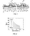
- FIG. 1illustrates a PFET and an NFET according to an embodiment of the invention.
- FIG. 2graphically illustrates magnitudes of compressive stress induced in a single-crystal silicon region of interest by a thin epitaxial layer of silicon germanium.
- FIGS. 3 through 11illustrate stages in fabrication of a PFET and an NFET according to an embodiment of the invention.
- FIGS. 12 through 18illustrates stages in fabrication of a PFET and an NFET according to another embodiment of the invention.
- FIGS. 19 through 21illustrate stages in fabrication of a PFET and an NFET according to yet another embodiment of the invention.
- FIG. 1illustrates a p-type field effect transistor (PFET) and an n-type field effect transistor (NFET) according to an embodiment of the invention.
- the NFET 10 and PFET 20are fabricated in a single-crystal semiconductor region 14 of a substrate 16 .
- the substrate 16may either be a bulk substrate or may preferably be a semiconductor-on-insulator substrate such as a silicon-on-insulator (SOI) substrate in which a relatively thin single-crystal region of a semiconductor is formed over an insulating layer 18 .
- SOIsilicon-on-insulator
- FETsfield effect transistors
- the substratepreferably includes a single-crystal silicon region 14 , and is more preferably an SOI substrate having a single-crystal silicon region 14 above an insulating layer 18 .
- the lattice-mismatched second semiconductoris preferably a different semiconductor such as silicon germanium or silicon carbide, and more preferably silicon germanium (Si x Ge y ) where x and y are percentages where x plus y equals 100 percent.
- Si x Ge ysilicon germanium
- the ranges of variation between x and ycan be rather large, y illustratively varying from 1% to 99%, and in such case, x consequently varying between 99% and 1%.
- the present inventionis not limited to the fabrication of transistors in a pure silicon crystal.
- the second semiconductorbeing lattice-mismatched to the first semiconductor, is formed by epitaxial growth in source and drain regions of the PFET in close proximity to the channel region of the PFET while the lattice-mismatched second semiconductor is simultaneously prevented from being formed in close proximity to the channel region of the NFET.
- FIG. 2is an aid to understanding principles on which the structure and method of the present embodiments of the invention are founded.
- FIG. 2graphically illustrates magnitudes of compressive stress induced in a single-crystal silicon region of interest by a thin epitaxial layer of silicon germanium that is laterally displaced from the region of interest.
- the curves in FIG. 2represent magnitudes of compressive stress, as mapped in relation to lateral displacement from the edge of the region of interest, for different percentage concentrations of germanium in the epitaxial layer.
- a SiGe layer having a Ge percentage of 37.5%applies a stress of 350 MPa to a region of a single-crystal silicon at a lateral displacement of 10 nm.
- the stressdecreases to 150 MPa at a lateral displacement of 30 nm.
- SiGe layers having lower percentagesare also graphed.
- a SiGe layer having a Ge percentage of 6.25%applies a stress of 75 MPa to a region of single-crystal silicon at a lateral displacement of 10 nm.
- the stressdecreases to about 30 MPa when applied at a lateral displacement of 30 nm.
- the other curves in the chartindicate that stress induced in the channel increases as the Ge content increases.
- the embodiments described hereintake advantage of the rapid decrease in stress with lateral displacement to form the PFET having the strain-inducing lattice-mismatched source and drain regions in close proximity to the channel region.
- the NFETis formed having the strain-inducing lattice-mismatched source and drain regions not in close proximity to the channel region.
- the teachings of the present inventionshall be understood to apply to the fabrication of transistors in other types of semiconductors such as in III-V compound semiconductors having a composition Al A In B Ga C As D P E N F , wherein A, B, C, D, E and F represent the respective percentages of each element Al, In, Ga, As, P and N in the semiconductor crystal, the percentages totaling 100.
- Gallium arsenide (GaAs), indium phosphide (InP), gallium nitride (GaN), and InGaAsPbeing common examples of such semiconductors.
- the PFET 20includes a channel region 22 disposed below a gate conductor preferably having a lower layer of heavily doped polysilicon 26 in contact with a gate dielectric 27 .
- the gate dielectric 27is preferably a layer of silicon dioxide thermally grown on the single-crystal semiconductor region 14 .
- halo regions 23 and extension regions 25are preferably disposed adjacent to the source and drain regions 24 in the vicinity of the channel region 22 .
- the polysilicon lower layer 26 of the gate conductoris preferably heavily doped to a concentration of about 10 19 cm ⁇ 3 .
- the polysilicon layer 26 of the PFET 20includes a p-type dopant such as boron for the purpose of matching the work function of the p-type conduction channel that exists when the PFET is turned on in operation.
- the gate conductorpreferably also includes a low-resistance portion 28 disposed above the polysilicon portion 26 .
- the low-resistance portion 28has much less resistance than the polysilicon portion 26 , and preferably includes a metal, a silicide of a metal, or both.
- the low-resistance portion 28includes a silicide formed by a self-aligned process (a “salicide”), being a silicide of any suitable metal including but not limited to tungsten, titanium and cobalt. More preferably, the silicide is a compound of cobalt (CoSi 2 ).
- the gate conductorcan include a metal layer in the place of a polysilicon layer in contact with the gate dielectric 27 , the metal layer preferably having been formed as a replacement gate after high temperature processing of the source and drain regions of the transistor has been completed.
- the source and drain regions 24 of the NFET 10 and PFET 20are formed in the single-crystal silicon region 16 , spaced from the channel regions 122 and 22 of the NFET 10 and the PFET 20 , respectively, by pairs of first spacers, second spacers 32 , and third spacers 34 .
- a pair of raised source-drain regions 36 including an epitaxial layer of silicon germanium 39 and a low-resistance layer 40are disposed over the source and drain regions 24 of the NFET 10 .
- a pair of raised source-drain regions 36 including a layer of silicon germanium 38 and a low-resistance layer 40are disposed over the source and drain regions 24 of the PFET 20 .
- the low-resistance layeris preferably a silicide formed in self-aligned manner, i.e. a “salicide”, from a metal deposited on the layers 38 , 39 of silicon germanium and thereafter reacted with the silicon germanium to form the silicide.
- the silicidecan be a compound of any suitable metal including but not limited to tungsten, titanium and cobalt. More preferably, the silicide is of cobalt, i.e. CoSi 2 .
- the layer of silicon germanium 38laterally extends to a sidewall of a first spacer 30 of the PFET 20 and under second and third spacers 32 and 34 .
- the epitaxial layer 38 of silicon germaniumis located in close proximity to the channel region 22 of the PFET to apply a compressive stress capable of benefiting hole mobility in the channel region 22 .
- the width of the first spacer 30is preferably 10 nm or less in order for the epitaxial layer 38 to apply a stress having a desirable magnitude to the channel region 22 .
- the epitaxial layer 39 in the NFET 10is laterally displaced from the channel region 122 by a distance spanning the width of at least the first and second spacers 30 , 32 . In such manner, the epitaxial layer 39 of silicon germanium is not located sufficiently close to the channel region 122 of the NFET to harmfully affect NFET performance.
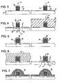
- FIGS. 3 through 12illustrate stages of a CMOS fabrication process according to an embodiment of the invention.
- a p-type field effect transistor (PFET) and an n-type field effect transistor (NFET)are formed.
- PFETp-type field effect transistor
- NFETn-type field effect transistor
- a stressis applied to the channel region in a first magnitude by a lattice-mismatched semiconductor layer.
- a stress in the first magnitudeis not applied since the lattice-mismatched semiconductor layer is not located in close proximity to the NFET channel region. In such manner, an increase in carrier mobility of the PFET is achieved while still maintaining desirable performance in the NFET.
- FIG. 3illustrates a stage in processing to form a PFET and an NFET according to an embodiment of the invention.
- a PFET gate stack 44 and an NFET gate stack 45are formed overlying a single-crystal semiconductor region 14 of a substrate.
- the single-crystal region 14consists essentially of a first semiconductor material as described above.
- the PFET gate stack 44includes a gate dielectric 27 overlying the single-crystal region 14 , a gate conductor layer 26 preferably including polysilicon in contact with the gate dielectric and an insulating cap 50 , preferably consisting essentially of silicon nitride.
- the NFET gate stack 45includes a gate dielectric 27 overlying the single-crystal region 14 , a gate conductor layer 26 preferably including polysilicon in contact with the gate dielectric 27 and an insulating cap 50 , preferably consisting essentially of silicon nitride.
- the gate conductors 26 of the PFET gate stack and the NFET gate stackare already provided at this stage with desired dopant types and concentrations to provide desirable work functions.
- the PFET gate stack 44may be provided with a p+ doped gate conductor layer 26 while the NFET gate stack 45 may be provided with an n+ doped gate conductor layer 26 .
- extension and halo implantsare preferably performed into the active area of the single-crystal region 14 adjacent to the NFET gate stack 45 , using the NFET gate stack 45 as a mask to prevent implants from penetrating too deeply into the channel region 122 below the NFET gate stack 45 .
- the active area adjacent to the PFET gate stack 44is prevented from being implanted, as by a block mask 42 preferably including a photoresist material.
- the spacers 30are preferably formed of a deposited nitride such as silicon nitride and are preferably thin, e.g. ranging from 3 nm to 20 nm in thickness, more preferably between 5 nm and 15 nm in thickness, and most preferably about 10 nm in thickness.
- extension and halo implantsare preferably performed into the active area of the single-crystal region 14 adjacent to the PFET gate stack 44 , using the PFET gate stack 44 as a mask to prevent implants from penetrating too deeply into the channel region 22 below the PFET gate stack 44 .
- the active area adjacent to the NFET gate stack 45is prevented from being implanted, as by a block mask 43 preferably including a photoresist material.
- the block mask 43is removed and a thick conformal material layer 46 is deposited over the PFET gate stack 44 and NFET gate stack 45 .
- the conformal material layer 46should be insulative rather than conductive or semiconductive in nature.
- the conformal material layer 46includes an oxide, preferably being silicon dioxide, and is preferably deposited at a low temperature such as from a tetraethylorthosilicate (TEOS) precursor.
- TEOStetraethylorthosilicate
- This processis preferably performed by depositing a conformal layer of silicon nitride and then vertically etching the structure as by a reactive ion etch (RIE) such that the spacers 48 remain on the sidewalls of the oxide layer 46 but the conformal nitride layer is removed from horizontal surfaces.
- RIEreactive ion etch
- the oxide layer 46is etched, as by RIE selective to nitride, from the top surface of the structures down to the level of the insulating caps 50 on both the PFET gate stack 44 and the NFET gate stack 45 . During such etch the oxide layer 46 is also removed from areas of the single-crystal region 14 that extend beyond the nitride spacers 48 on each of the PFET gate stack 44 and the NFET gate stack 45 .
- the nitride spacers 48protect the sidewalls of the structures from being etched, and the insulating caps 50 protect the gate conductors 26 of the PFET gate stack and the NFET gate stack from damage and/or being etched.
- a block mask 52is again applied over an area including the NFET gate stack 45 while the PFET gate stack 44 remains exposed.
- the block mask 52preferably includes a photoresist material. With the block mask 52 in place, the oxide layer 46 adhering to the PFET gate stack 44 is undercut, as by an isotropic wet chemical etch selective to nitride. This results in the oxide layer 46 having the appearance shown in FIG. 10 . As a result of this etch, the main surface 54 of the single-crystal semiconductor region 14 is exposed.
- the second semiconductoris preferably silicon germanium having a higher percentage of germanium than that of the single-crystal semiconductor region 14 , whether or not that region 14 has any germanium content or not.
- this layer 38is formed under the undercut portion 56 of the oxide layer 46 such that it applies a compressive stress in close proximity to the channel region 22 of the PFET 20 , the layer 38 being laterally spaced from the channel region 22 only by the first nitride spacer 30 .
- the silicon germanium layer 39is not formed in as close proximity to the gate conductor 26 such that it does not apply a compressive stress to the channel region 122 of the NFET in as great a magnitude as the compressive stress applied to the channel region 22 of the PFET because a compressive stress hinders electron mobility in an NFET.
- the lattice-mismatched semiconductor layer that induces the stressis displaced an adequate distance from the channel region 122 of the NFET 10 , then the compressive stress can be tolerated, as described above relative to FIG. 2 .
- parameters of the spacers 30 and oxide layer 46can be tailored to apply a lower magnitude counter stress to improve electron mobility in the NFET. Such counter stress would be applied as a low magnitude tensile stress to counter the effects of the low magnitude compressive stress applied by the silicon germanium layer 39 in the NFET channel region 122 .
- FIG. 1A final processing stage of this embodiment is illustrated in FIG. 1 .
- source and drain regions 24 of the PFET 20are implanted into the single-crystal region 14 using the PFET gate stack 44 structure including the gate conductor 26 , first spacers 30 , second spacers 32 and third spacers 34 as a mask while areas of the NFET 10 are protected from such implanting by a block mask (not shown).
- source and drain regions 24 of the NFET 10are implanted into the single-crystal region 14 using the NFET gate stack 45 including the gate conductor 26 , first spacers 30 , second spacers 32 and third spacers 34 as a mask while the PFET 20 is protected from such implanting by a block mask (not shown). Thereafter, high temperature processing can be performed to anneal the implanted source and drain regions 24 and to drive the implanted dopant to the desired depth and lateral dimensions.
- nitride insulating caps 50are removed from the PFET gate stack 44 and the NFET gate stack 45 .
- a silicide-forming metalis then deposited over the structures shown and then reacted by high temperature processing with the semiconductor material of a polysilicon gate conductor 26 in contact therewith and with the layers 38 and 39 of silicon germanium in contact therewith to form a self-aligned silicide (“salicide”) 40 .
- the nitride insulating caps 50 and the polysilicon gate conductors 26can be removed from between the spacers 30 , 32 as by RIE selective to nitride and oxide and a metal replacement gate be formed in its place.
- the gate dielectric formed prior theretopreferably functions as an etch stop layer, i.e. as a sacrificial layer, for the polysilicon RIE.
- the first formed gate dielectricis removed after the RIE removal of the polysilicon gate 26 due to damage suffered by that layer during RIE. Thereafter, a second gate dielectric 27 is deposited in the place formerly occupied by the removed first gate dielectric.
- the metal gate conductoris then deposited in the openings formed thereby between the spacers 30 , 32 as a conformal layer over the layers 38 , 39 of the single-crystal silicon germanium. In such way, a metal replacement gate is formed after substantially completing processing of the PFET 20 and NFET 10 .
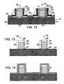
- FIG. 12Another embodiment of a PFET 220 and an NFET 210 formed according to the invention is illustrated in FIG. 12 .
- a lattice-mismatched semiconductor layer 238 of a PFETis formed as a raised layer contacting the single-crystal semiconductor region 214 in close proximity to the channel region 322 of the PFET.
- a lattice-mismatched semiconductor layer 239is formed as a raised layer but not in as close proximity to the channel region 222 of the NFET 210 due to the presence of an additional spacer 231 between the layer 239 and the channel region 222 .
- a compressive stressis applied in different magnitudes to the channel regions 222 , 322 of both the NFET and PFET by the layers 239 , 238 .
- the amount of a strain created in the channel region of the NFET 210can be tailored based on the width 240 of the second spacer 231 . As discussed above, a greater lateral displacement of the layer 239 from the channel region 222 of the NFET 210 creates a lower strain in the channel region 222 of the NFET. Lower strain, in turn, affects electron mobility in the NFET 210 less negatively than a higher strain. In this embodiment, such lower strain can be achieved by the use of an appropriately sized spacer consisting essentially of a material such as silicon nitride.
- the spacer 231has a width 240 determined by a thickness of a deposited conformal silicon nitride material. If still lower strain is needed in the channel region 222 of the NFET 210 , the thickness of the silicon nitride spacer 231 can be made larger by depositing that layer to a greater thickness.
- a PFET gate stack 244 and an NFET gate stack 245each include a polysilicon gate 226 overlying a gate dielectric 227 preferably of a thermally grown oxide on a single-crystal semiconductor region 214 of a substrate such as a single-crystal silicon region. Insulating caps 250 overlie the polysilicon gates 226 . Pairs of first spacers 230 are formed on sidewalls of the polysilicon gates 226 after patterning and etching the gate stack structures 244 , 245 . These first spacers 230 are preferably thin, ranging in width between 3 nm and 20 nm, more preferably between 5 nm and 15 nm, and most preferably about 10 nm in width.
- halo and extension ion implantsare performed into source and drain regions (not shown) of the PFET 220 and the NFET 210 adjacent to the spacers, preferably by block masking NFET regions while implanting the PFET regions and then block masking PFET regions while implanting the NFET regions.
- second pairs of spacers 231are formed on sidewalls of the first pairs of spacers 230 . This is done by a process of depositing a conformal material such as silicon nitride, and thereafter vertically etching the structure, as by RIE, to provide the structure shown in FIG. 15 .
- a block mask 243is applied over the NFET gate stack 245 and adjacent areas.
- the second spacers 231are then removed from the PFET gate stack 244 .
- a layer of silicon germanium 238is selectively grown over the single-crystal region 214 of the substrate. Due to presence of the second spacers 231 on sidewalls of the NFET gate stack 245 , the layer 238 of silicon germanium is laterally displaced from the channel region 222 of the NFET by a greater distance (e.g. by the width 240 of the spacer 231 ) than it is to the channel region 322 of the PFET. In such manner, greater hole mobility is achieved in the PFET without severely affecting electron mobility in the NFET.
- spacers 232 and 234are formed. These spacers 232 and 234 are used to space the final raised silicided source and drain regions 224 ( FIG. 12 ) from the channel regions 222 and 322 of the NFET and the PFET respectively.
- These spacers 232 , 234preferably include nitride and oxide, respectively.
- spacer 232consists essentially of nitride and spacer 234 consists essentially of oxide.
- additional RIE etchesare performed, resulting in the structure shown in FIG. 18 .
- self-aligned silicide layers 224are formed in areas of layer 238 that are not covered by the gate stacks 244 and 245 , as shown in FIG. 12 .
- FIGS. 19-21A further embodiment of the invention is illustrated in FIGS. 19-21 .
- the silicon germanium layer 338does not form a part of the NFET structure 310 , as shown in FIG. 19 . Rather, that layer 338 is disposed only in the PFET structure 320 . In such manner, a compressive stress is applied to the channel region 422 of the PFET 320 but not to the channel region 423 of the NFET 310 .
- FIGS. 20 and 21A process for fabricating the PFET 320 and NFET 310 is illustrated in FIGS. 20 and 21 .
- a PFET gate stack 344 and an NFET gate stack 345are formed, each including a polysilicon gate 326 overlying a gate dielectric 327 preferably consisting of a thermally grown oxide, an insulating cap 350 , preferably including silicon nitride, and a first pair of spacers 330 , preferably including silicon nitride. Halo and extension implants can be performed at this time.
- a conformal material layer 360is deposited and then patterned to cover only the active areas of the single-crystal semiconductor region 314 adjacent to the NFET gate stack 345 .
- Such conformal material layercan illustratively be an oxide, a nitride, or a combination of both.
- the conformal material layer 360includes a nitride such as silicon nitride.
- a lattice-mismatched semiconductor 338such as silicon germanium is epitaxially grown onto the exposed active areas of the single-crystal region 314 adjacent to the PFET gate stack 344 .
- additional insulating layersare deposited over the conformal layer 360 and then the layers are vertically etched, as by RIE to form spacers 331 and additional spacers 332 and 334 in a manner such as that described above with reference to FIG. 18 .
- self-aligned silicide regions 324 and 424are preferably formed in both the PFET 320 and NFET 310 , in a manner such as that described above relative to FIG. 12 .
Landscapes
- Physics & Mathematics (AREA)
- High Energy & Nuclear Physics (AREA)
- Engineering & Computer Science (AREA)
- General Physics & Mathematics (AREA)
- Health & Medical Sciences (AREA)
- Toxicology (AREA)
- Crystallography & Structural Chemistry (AREA)
- Condensed Matter Physics & Semiconductors (AREA)
- Chemical & Material Sciences (AREA)
- Manufacturing & Machinery (AREA)
- Computer Hardware Design (AREA)
- Microelectronics & Electronic Packaging (AREA)
- Power Engineering (AREA)
- Metal-Oxide And Bipolar Metal-Oxide Semiconductor Integrated Circuits (AREA)
- Insulated Gate Type Field-Effect Transistor (AREA)
- Thin Film Transistor (AREA)
Abstract
Description
- The present invention relates to the fabrication of semiconductor integrated circuits, and more specifically to an apparatus and method of making strained channel complementary metal oxide semiconductor (CMOS) transistors having epitaxial lattice-mismatched epitaxial extension and source and drain regions.
- Both theoretical and empirical studies have demonstrated that carrier mobility in a transistor can be greatly increased when a stress of sufficient magnitude is applied to the conduction channel of a transistor to create a strain therein. Stress is defined as force per unit area. Strain is a dimensionless quantity defined as the change in a particular dimension of an item: for example, the change in the item's length, versus the initial dimension of that item: for example, its original length, when a force is applied in the direction of that dimension of the item: for example, in the direction of the length of the item's length. Strain can be either tensile or compressive. In p-type field effect transistors, the application of a compressive longitudinal stress, i.e. in the direction of the length of the conduction channel, creates a strain in the conduction channel which is known to increase the drive current of a PFET. However, if that same stress is applied to the conduction channel of an NFET, its drive current decreases.
- It has been proposed to increase the performance of an NFET and a PFET by applying a tensile longitudinal stress to the conduction channel of an NFET and applying a compressive longitudinal stress to the conduction channel of a PFET. Such proposals have focused on masked processes involving the masking of a PFET portion of the chip and altering the materials used in shallow trench isolation regions near the conduction channel of the PFET to apply a desired stress thereto. Separate steps would then be performed to mask the NFET portion of the chip and alter the materials used in shallow trench isolation regions near the conduction channels of the NFET to apply a desired stress thereto. Other proposals have involved masked processes centered on modulating intrinsic stresses present in spacer features.
- Silicon germanium is a desirable lattice-mismatched semiconductor for use in forming strained silicon transistor channels. A strain is created when a second semiconductor is grown onto a single-crystal of a first semiconductor when the two semiconductors are lattice-mismatched to each other. Silicon and silicon germanium are lattice-mismatched to each other such that the growth of one of them onto the other produces a strain in each which can be either tensile or compressive.
- Silicon germanium grows epitaxially on silicon having a crystal structure aligned with the silicon crystal structure. However, because silicon germanium normally has a larger crystal structure than silicon, the epitaxially grown silicon germanium becomes internally compressed.
- In other proposals using strained silicon, a substrate includes a very thick layer of silicon germanium. Alternatively, the bulk substrate consists of single-crystal silicon germanium. In either case, the silicon germanium layer or substrate is known as a relaxed layer because the strain is released by dislocations which form within the silicon germanium layer. When a single-crystal silicon layer is grown epitaxially on a relaxed layer of single-crystal SiGe, a tensile strain is produced in the epitaxially grown silicon crystal layer. This results in improved electron mobility, which improves the performance of an NFET.
- However, such technique requires the SiGe to be relaxed, which requires that the SiGe layer be very thick, i.e. at least 0.5 to 1.0 μm thick. Improvements in the mobility of holes is difficult to obtain because to do so, the SiGe layer requires a large percentage of germanium, which can result in excessive dislocations in the SiGe crystal, causing yield problems. Further, processing costs can be prohibitive.
- Other techniques such as graded Ge concentration and chemical mechanical polishing methods are used to improve the quality of the films. However, those techniques are plagued by high cost and high defect density.
- Accordingly, it would be desirable to create a strain in the channel region of a PFET without the use of a thick SiGe crystal region. It would be desirable create a desired strain in a channel region of a device using an epitaxially grown SiGe film in source and drain regions of the PFET.
- It would further be desirable for the SiGe film to be formed sufficiently thin to enable the SiGe film to apply a desirably high magnitude stress and avoid the SiGe film from becoming a relaxed film.
- It would further be desirable to create a compressive strain to increase hole mobility in the channel region of a PFET by growing an epitaxial layer of SiGe in the source and drain regions of the PFET.
- It would further be desirable to provide a process of forming raised source and drain regions extending above a level of the gate dielectric which include the lattice-mismatched semiconductor for creating a desirable strain in the channel region of the PFET.
- It would further be desirable to provide a process for creating a desired strain in the channel region of a PFET without creating the same strain in the channel region of the NFET.
- It would further be desirable to provide a structure and method for forming a lattice-mismatched semiconductor layer in source and drain regions of a PFET in close proximity to the channel region of the PFET while preventing the lattice-mismatched semiconductor layer from being formed in close proximity to the channel region of an NFET of the same integrated circuit.
- It would further be desirable to provide a structure and method for forming a lattice-mismatched semiconductor layer in extension regions of a PFET in close proximity to the channel region of the PFET while preventing the lattice-mismatched semiconductor layer from being formed in extension regions in close proximity to the channel region of an NFET of the same integrated circuit.
- According to an aspect of the invention, an integrated circuit having complementary metal oxide semiconductor (CMOS) transistors including a p-type field effect transistor (PFET) and an n-type field effect transistor (NFET) is provided. The NFET and the PFET each have a channel region disposed in a single-crystal layer of a first semiconductor, wherein a stress is applied at a first magnitude to a channel region of the PFET but not to a channel region of the NFET. The stress is applied by a layer of a second semiconductor which is lattice-mismatched to the first semiconductor. The layer of second semiconductor is formed in source and drain regions of the PFET a first distance from the channel region of the PFET. The layer of second semiconductor is further formed in source and drain regions of the NFET at a second distance from the channel region of the NFET, the second distance being greater than the first distance.
- According to another aspect of the invention, a method is provided of fabricating an integrated circuit including a p-type field effect transistor (PFET) and an n-type field effect transistor (NFET). The NFET and the PFET each have a channel region disposed in a single-crystal region of a first semiconductor, a stress being applied to the channel region of said PFET in a first magnitude and not being applied to the channel region of the NFET at that first magnitude.
- According to a preferred aspect of that method, a PFET gate stack and an NFET gate stack are formed over a single-crystal region of a first semiconductor, the PFET gate stack and the NFET gate stack each having a gate conductor overlying a gate dielectric formed on a main surface of the single-crystal region of a first semiconductor and first spacers including a first material formed on sidewalls of the gate conductor. Second spacers are formed on side-walls of the first spacers of the PFET gate stack and the NFET gate stack, the second spacers including a second material. Then, portions of the second material are removed from the second spacers of the PFET gate stack selective to the first material while protecting the second material from being removed from the second spacers of the NFET gate stack. Thereafter, a layer of a second semiconductor is grown on exposed areas of the single-crystal region of the first semiconductor, the second semiconductor being lattice-mismatched to the first semiconductor, such that a stress is applied to the channel region of said PFET at a first magnitude and not applied to the channel region of the NFET at the first magnitude. Source and drain regions are fabricated to complete the PFET and the NFET.
FIG. 1 illustrates a PFET and an NFET according to an embodiment of the invention.FIG. 2 graphically illustrates magnitudes of compressive stress induced in a single-crystal silicon region of interest by a thin epitaxial layer of silicon germanium.FIGS. 3 through 11 illustrate stages in fabrication of a PFET and an NFET according to an embodiment of the invention.FIGS. 12 through 18 illustrates stages in fabrication of a PFET and an NFET according to another embodiment of the invention.FIGS. 19 through 21 illustrate stages in fabrication of a PFET and an NFET according to yet another embodiment of the invention.FIG. 1 illustrates a p-type field effect transistor (PFET) and an n-type field effect transistor (NFET) according to an embodiment of the invention. As illustrated inFIG. 1 , the NFET10 andPFET 20 are fabricated in a single-crystal semiconductor region 14 of asubstrate 16. Thesubstrate 16 may either be a bulk substrate or may preferably be a semiconductor-on-insulator substrate such as a silicon-on-insulator (SOI) substrate in which a relatively thin single-crystal region of a semiconductor is formed over aninsulating layer 18. When field effect transistors (FETs) are formed in such SOI substrates, faster switching operation is often achieved than otherwise, because junction capacitance between the channel region of the transistor and the bulk substrate is eliminated. The substrate preferably includes a single-crystal silicon region 14, and is more preferably an SOI substrate having a single-crystal silicon region 14 above aninsulating layer 18.- As described in this and the embodiments to follow, reference will be made to the fabrication of NFET and PFET transistors having channel regions disposed within a single-crystal region of a substrate preferably consisting essentially of a first semiconductor such as silicon. As the first semiconductor is preferably silicon, the lattice-mismatched second semiconductor is preferably a different semiconductor such as silicon germanium or silicon carbide, and more preferably silicon germanium (SixGey) where x and y are percentages where x plus y equals 100 percent. The ranges of variation between x and y can be rather large, y illustratively varying from 1% to 99%, and in such case, x consequently varying between 99% and 1%.
- However, the present invention is not limited to the fabrication of transistors in a pure silicon crystal. The single crystal region of the
substrate 14 may consist essentially of silicon germanium in proportions according to a first formula Six1Gey1, where x1 and y1 are percentages where x1+y1=100%, and the layer of the second semiconductor consists essentially of silicon germanium in different proportions according to a second formula Six2Gey2where x1 and y1 are percentages where x2+y2=100%, x1 being not equal to x2, and yl being not equal to y2. The second semiconductor, being lattice-mismatched to the first semiconductor, is formed by epitaxial growth in source and drain regions of the PFET in close proximity to the channel region of the PFET while the lattice-mismatched second semiconductor is simultaneously prevented from being formed in close proximity to the channel region of the NFET. FIG. 2 is an aid to understanding principles on which the structure and method of the present embodiments of the invention are founded.FIG. 2 graphically illustrates magnitudes of compressive stress induced in a single-crystal silicon region of interest by a thin epitaxial layer of silicon germanium that is laterally displaced from the region of interest. The curves inFIG. 2 represent magnitudes of compressive stress, as mapped in relation to lateral displacement from the edge of the region of interest, for different percentage concentrations of germanium in the epitaxial layer.- As shown in
FIG. 2 , a SiGe layer having a Ge percentage of 37.5% applies a stress of 350 MPa to a region of a single-crystal silicon at a lateral displacement of 10 nm. However, as the lateral displacement from the SiGe layer is increased, the magnitude of the stress decreases rapidly. For the same Ge percentage of 37.5%, the stress decreases to 150 MPa at a lateral displacement of 30 nm. SiGe layers having lower percentages are also graphed. A SiGe layer having a Ge percentage of 6.25% applies a stress of 75 MPa to a region of single-crystal silicon at a lateral displacement of 10 nm. However, the stress decreases to about 30 MPa when applied at a lateral displacement of 30 nm. The other curves in the chart indicate that stress induced in the channel increases as the Ge content increases. - The embodiments described herein take advantage of the rapid decrease in stress with lateral displacement to form the PFET having the strain-inducing lattice-mismatched source and drain regions in close proximity to the channel region. On the other hand, the NFET is formed having the strain-inducing lattice-mismatched source and drain regions not in close proximity to the channel region.
- The teachings of the present invention shall be understood to apply to the fabrication of transistors in other types of semiconductors such as in III-V compound semiconductors having a composition AlAInBGaCAsDPENF, wherein A, B, C, D, E and F represent the respective percentages of each element Al, In, Ga, As, P and N in the semiconductor crystal, the percentages totaling 100. Gallium arsenide (GaAs), indium phosphide (InP), gallium nitride (GaN), and InGaAsP being common examples of such semiconductors.
- As further shown in
FIG. 1 , thePFET 20 includes achannel region 22 disposed below a gate conductor preferably having a lower layer of heavily dopedpolysilicon 26 in contact with agate dielectric 27. Thegate dielectric 27 is preferably a layer of silicon dioxide thermally grown on the single-crystal semiconductor region 14. Preferably,halo regions 23 andextension regions 25 are preferably disposed adjacent to the source and drainregions 24 in the vicinity of thechannel region 22. - The polysilicon
lower layer 26 of the gate conductor is preferably heavily doped to a concentration of about 1019cm−3. Preferably, thepolysilicon layer 26 of thePFET 20 includes a p-type dopant such as boron for the purpose of matching the work function of the p-type conduction channel that exists when the PFET is turned on in operation. The gate conductor preferably also includes a low-resistance portion 28 disposed above thepolysilicon portion 26. The low-resistance portion 28 has much less resistance than thepolysilicon portion 26, and preferably includes a metal, a silicide of a metal, or both. In a preferred embodiment, the low-resistance portion 28 includes a silicide formed by a self-aligned process (a “salicide”), being a silicide of any suitable metal including but not limited to tungsten, titanium and cobalt. More preferably, the silicide is a compound of cobalt (CoSi2). - Alternatively, the gate conductor can include a metal layer in the place of a polysilicon layer in contact with the
gate dielectric 27, the metal layer preferably having been formed as a replacement gate after high temperature processing of the source and drain regions of the transistor has been completed. - The source and drain
regions 24 of theNFET 10 andPFET 20 are formed in the single-crystal silicon region 16, spaced from thechannel regions NFET 10 and thePFET 20, respectively, by pairs of first spacers,second spacers 32, andthird spacers 34. A pair of raised source-drain regions 36 including an epitaxial layer ofsilicon germanium 39 and a low-resistance layer 40 are disposed over the source and drainregions 24 of theNFET 10. A pair of raised source-drain regions 36 including a layer ofsilicon germanium 38 and a low-resistance layer 40 are disposed over the source and drainregions 24 of thePFET 20. The low-resistance layer is preferably a silicide formed in self-aligned manner, i.e. a “salicide”, from a metal deposited on thelayers - As shown in
FIG. 1 , the layer ofsilicon germanium 38 laterally extends to a sidewall of afirst spacer 30 of thePFET 20 and under second andthird spacers epitaxial layer 38 of silicon germanium is located in close proximity to thechannel region 22 of the PFET to apply a compressive stress capable of benefiting hole mobility in thechannel region 22. The width of thefirst spacer 30 is preferably 10 nm or less in order for theepitaxial layer 38 to apply a stress having a desirable magnitude to thechannel region 22. - In contrast to the
PFET 20, theepitaxial layer 39 in theNFET 10 is laterally displaced from thechannel region 122 by a distance spanning the width of at least the first andsecond spacers epitaxial layer 39 of silicon germanium is not located sufficiently close to thechannel region 122 of the NFET to harmfully affect NFET performance. FIGS. 3 through 12 illustrate stages of a CMOS fabrication process according to an embodiment of the invention. As a result of processing according to the embodiment, a p-type field effect transistor (PFET) and an n-type field effect transistor (NFET) are formed. In the PFET, a stress is applied to the channel region in a first magnitude by a lattice-mismatched semiconductor layer. On the other hand, in the channel region of the NFET, a stress in the first magnitude is not applied since the lattice-mismatched semiconductor layer is not located in close proximity to the NFET channel region. In such manner, an increase in carrier mobility of the PFET is achieved while still maintaining desirable performance in the NFET.FIG. 3 illustrates a stage in processing to form a PFET and an NFET according to an embodiment of the invention. As shown inFIG. 3 , aPFET gate stack 44 and anNFET gate stack 45 are formed overlying a single-crystal semiconductor region 14 of a substrate. The single-crystal region 14 consists essentially of a first semiconductor material as described above. ThePFET gate stack 44 includes agate dielectric 27 overlying the single-crystal region 14, agate conductor layer 26 preferably including polysilicon in contact with the gate dielectric and an insulatingcap 50, preferably consisting essentially of silicon nitride. TheNFET gate stack 45 includes agate dielectric 27 overlying the single-crystal region 14, agate conductor layer 26 preferably including polysilicon in contact with thegate dielectric 27 and an insulatingcap 50, preferably consisting essentially of silicon nitride.- In an embodiment, the
gate conductors 26 of the PFET gate stack and the NFET gate stack are already provided at this stage with desired dopant types and concentrations to provide desirable work functions. For example, thePFET gate stack 44 may be provided with a p+ dopedgate conductor layer 26 while theNFET gate stack 45 may be provided with an n+ dopedgate conductor layer 26. - Next, as shown in
FIG. 4 , extension and halo implants are preferably performed into the active area of the single-crystal region 14 adjacent to theNFET gate stack 45, using theNFET gate stack 45 as a mask to prevent implants from penetrating too deeply into thechannel region 122 below theNFET gate stack 45. During such implants, the active area adjacent to thePFET gate stack 44 is prevented from being implanted, as by ablock mask 42 preferably including a photoresist material. - Next, as shown in
FIG. 5 , theblock mask 42 is removed and pairs offirst spacers 30 are formed on the sidewalls of thePFET gate stack 25 andNFET gate stack 45. Thespacers 30 are preferably formed of a deposited nitride such as silicon nitride and are preferably thin, e.g. ranging from 3 nm to 20 nm in thickness, more preferably between 5 nm and 15 nm in thickness, and most preferably about 10 nm in thickness. - Next, as shown in
FIG. 6 , extension and halo implants are preferably performed into the active area of the single-crystal region 14 adjacent to thePFET gate stack 44, using thePFET gate stack 44 as a mask to prevent implants from penetrating too deeply into thechannel region 22 below thePFET gate stack 44. During such implants, the active area adjacent to theNFET gate stack 45 is prevented from being implanted, as by ablock mask 43 preferably including a photoresist material. - Thereafter, as shown in
FIG. 7 , theblock mask 43 is removed and a thickconformal material layer 46 is deposited over thePFET gate stack 44 andNFET gate stack 45. Theconformal material layer 46 should be insulative rather than conductive or semiconductive in nature. Preferably, theconformal material layer 46 includes an oxide, preferably being silicon dioxide, and is preferably deposited at a low temperature such as from a tetraethylorthosilicate (TEOS) precursor. Hereinafter, the material of thislayer 46 is referred to as “oxide”. - Next, as shown in
FIG. 8 , an additional, i.e. a third, pair of spacers48 preferably including a nitride material, more preferably being silicon nitride, is formed over theoxide layer 46 on both thePFET gate stack 44 and theNFET gate stack 45. This process is preferably performed by depositing a conformal layer of silicon nitride and then vertically etching the structure as by a reactive ion etch (RIE) such that the spacers48 remain on the sidewalls of theoxide layer 46 but the conformal nitride layer is removed from horizontal surfaces. - Next, as shown in
FIG. 9 , after the nitride spacers48 are in place, theoxide layer 46 is etched, as by RIE selective to nitride, from the top surface of the structures down to the level of the insulatingcaps 50 on both thePFET gate stack 44 and theNFET gate stack 45. During such etch theoxide layer 46 is also removed from areas of the single-crystal region 14 that extend beyond the nitride spacers48 on each of thePFET gate stack 44 and theNFET gate stack 45. During such etch, the nitride spacers48 protect the sidewalls of the structures from being etched, and the insulatingcaps 50 protect thegate conductors 26 of the PFET gate stack and the NFET gate stack from damage and/or being etched. - Thereafter, as shown in
FIG. 10 , ablock mask 52 is again applied over an area including theNFET gate stack 45 while thePFET gate stack 44 remains exposed. Theblock mask 52 preferably includes a photoresist material. With theblock mask 52 in place, theoxide layer 46 adhering to thePFET gate stack 44 is undercut, as by an isotropic wet chemical etch selective to nitride. This results in theoxide layer 46 having the appearance shown inFIG. 10 . As a result of this etch, themain surface 54 of the single-crystal semiconductor region 14 is exposed. - Thereafter, as shown in
FIG. 11 , a single-crystal layer of a second semiconductor, lattice-mismatched to the first semiconductor, is epitaxially grown onto the main surface of the single-crystal semiconductor region 14. As described above relative toFIG. 1 , the second semiconductor is preferably silicon germanium having a higher percentage of germanium than that of the single-crystal semiconductor region 14, whether or not thatregion 14 has any germanium content or not. In the PFET region, thislayer 38 is formed under the undercutportion 56 of theoxide layer 46 such that it applies a compressive stress in close proximity to thechannel region 22 of thePFET 20, thelayer 38 being laterally spaced from thechannel region 22 only by thefirst nitride spacer 30. - On the other hand, in the NFET the
silicon germanium layer 39 is not formed in as close proximity to thegate conductor 26 such that it does not apply a compressive stress to thechannel region 122 of the NFET in as great a magnitude as the compressive stress applied to thechannel region 22 of the PFET because a compressive stress hinders electron mobility in an NFET. However, if the lattice-mismatched semiconductor layer that induces the stress is displaced an adequate distance from thechannel region 122 of theNFET 10, then the compressive stress can be tolerated, as described above relative toFIG. 2 . Additionally, parameters of thespacers 30 andoxide layer 46 can be tailored to apply a lower magnitude counter stress to improve electron mobility in the NFET. Such counter stress would be applied as a low magnitude tensile stress to counter the effects of the low magnitude compressive stress applied by thesilicon germanium layer 39 in theNFET channel region 122. - A final processing stage of this embodiment is illustrated in
FIG. 1 . During this stage of processing, source and drainregions 24 of thePFET 20 are implanted into the single-crystal region 14 using thePFET gate stack 44 structure including thegate conductor 26,first spacers 30,second spacers 32 andthird spacers 34 as a mask while areas of theNFET 10 are protected from such implanting by a block mask (not shown). In a preferably separate implant step, source and drainregions 24 of theNFET 10 are implanted into the single-crystal region 14 using theNFET gate stack 45 including thegate conductor 26,first spacers 30,second spacers 32 andthird spacers 34 as a mask while thePFET 20 is protected from such implanting by a block mask (not shown). Thereafter, high temperature processing can be performed to anneal the implanted source and drainregions 24 and to drive the implanted dopant to the desired depth and lateral dimensions. - At this time, the
nitride insulating caps 50 are removed from thePFET gate stack 44 and theNFET gate stack 45. Preferably, a silicide-forming metal is then deposited over the structures shown and then reacted by high temperature processing with the semiconductor material of apolysilicon gate conductor 26 in contact therewith and with thelayers regions 24, thenitride insulating caps 50 and thepolysilicon gate conductors 26 can be removed from between thespacers polysilicon gate 26 due to damage suffered by that layer during RIE. Thereafter, asecond gate dielectric 27 is deposited in the place formerly occupied by the removed first gate dielectric. The metal gate conductor is then deposited in the openings formed thereby between thespacers layers PFET 20 andNFET 10. - Another embodiment of a
PFET 220 and anNFET 210 formed according to the invention is illustrated inFIG. 12 . In this embodiment, as many as four pairs of spacers are utilized in theNFET 210 for displacing raised silicided source and drain regions224 a desirable distance from the channel region of theNFET 210 and for displacing raised silicided source and drain regions224 a desirable distance from the channel region of thePFET 220. As further shown inFIG. 12 , a lattice-mismatchedsemiconductor layer 238 of a PFET is formed as a raised layer contacting the single-crystal semiconductor region 214 in close proximity to thechannel region 322 of the PFET. In theNFET 210, a lattice-mismatched semiconductor layer239 is formed as a raised layer but not in as close proximity to thechannel region 222 of theNFET 210 due to the presence of anadditional spacer 231 between the layer239 and thechannel region 222. In this embodiment, a compressive stress is applied in different magnitudes to thechannel regions layers 239,238. - In this embodiment, the amount of a strain created in the channel region of the
NFET 210 can be tailored based on the width240 of thesecond spacer 231. As discussed above, a greater lateral displacement of the layer239 from thechannel region 222 of theNFET 210 creates a lower strain in thechannel region 222 of the NFET. Lower strain, in turn, affects electron mobility in theNFET 210 less negatively than a higher strain. In this embodiment, such lower strain can be achieved by the use of an appropriately sized spacer consisting essentially of a material such as silicon nitride. - The
spacer 231 has a width240 determined by a thickness of a deposited conformal silicon nitride material. If still lower strain is needed in thechannel region 222 of theNFET 210, the thickness of thesilicon nitride spacer 231 can be made larger by depositing that layer to a greater thickness. - Stages in fabrication of the embodiment will now be described relative to
FIGS. 13 through 18 . As shown inFIG. 13 , aPFET gate stack 244 and anNFET gate stack 245 each include apolysilicon gate 226 overlying agate dielectric 227 preferably of a thermally grown oxide on a single-crystal semiconductor region 214 of a substrate such as a single-crystal silicon region. Insulatingcaps 250 overlie thepolysilicon gates 226. Pairs offirst spacers 230 are formed on sidewalls of thepolysilicon gates 226 after patterning and etching thegate stack structures first spacers 230 are preferably thin, ranging in width between 3 nm and 20 nm, more preferably between 5 nm and 15 nm, and most preferably about 10 nm in width. - After forming the
spacers 230, halo and extension ion implants are performed into source and drain regions (not shown) of thePFET 220 and theNFET 210 adjacent to the spacers, preferably by block masking NFET regions while implanting the PFET regions and then block masking PFET regions while implanting the NFET regions. Thereafter, as shown inFIGS. 14 and 15 , second pairs ofspacers 231 are formed on sidewalls of the first pairs ofspacers 230. This is done by a process of depositing a conformal material such as silicon nitride, and thereafter vertically etching the structure, as by RIE, to provide the structure shown inFIG. 15 . - Thereafter, as shown in
FIG. 16 , a block mask243 is applied over theNFET gate stack 245 and adjacent areas. Thesecond spacers 231 are then removed from thePFET gate stack 244. Next, as shown inFIG. 17 , a layer ofsilicon germanium 238 is selectively grown over the single-crystal region 214 of the substrate. Due to presence of thesecond spacers 231 on sidewalls of theNFET gate stack 245, thelayer 238 of silicon germanium is laterally displaced from thechannel region 222 of the NFET by a greater distance (e.g. by the width240 of the spacer231) than it is to thechannel region 322 of the PFET. In such manner, greater hole mobility is achieved in the PFET without severely affecting electron mobility in the NFET. - Next, as shown in
FIG. 18 ,further spacers spacers FIG. 12 ) from thechannel regions spacers spacer 232 consists essentially of nitride andspacer 234 consists essentially of oxide. During this process, additional RIE etches are performed, resulting in the structure shown inFIG. 18 . Finally, self-aligned silicide layers224 are formed in areas oflayer 238 that are not covered by the gate stacks244 and245, as shown inFIG. 12 . - A further embodiment of the invention is illustrated in
FIGS. 19-21 . In contrast to the embodiment illustrated relative toFIGS. 12-18 , in this embodiment, thesilicon germanium layer 338 does not form a part of theNFET structure 310, as shown inFIG. 19 . Rather, thatlayer 338 is disposed only in thePFET structure 320. In such manner, a compressive stress is applied to thechannel region 422 of thePFET 320 but not to thechannel region 423 of theNFET 310. - A process for fabricating the
PFET 320 andNFET 310 is illustrated inFIGS. 20 and 21 . As shown inFIG. 20 , aPFET gate stack 344 and anNFET gate stack 345 are formed, each including apolysilicon gate 326 overlying agate dielectric 327 preferably consisting of a thermally grown oxide, an insulatingcap 350, preferably including silicon nitride, and a first pair ofspacers 330, preferably including silicon nitride. Halo and extension implants can be performed at this time. - Thereafter, a
conformal material layer 360 is deposited and then patterned to cover only the active areas of the single-crystal semiconductor region 314 adjacent to theNFET gate stack 345. Such conformal material layer can illustratively be an oxide, a nitride, or a combination of both. Preferably, theconformal material layer 360 includes a nitride such as silicon nitride. Thereafter, a lattice-mismatchedsemiconductor 338 such as silicon germanium is epitaxially grown onto the exposed active areas of the single-crystal region 314 adjacent to thePFET gate stack 344. - Thereafter, as illustrated in
FIG. 21 , additional insulating layers are deposited over theconformal layer 360 and then the layers are vertically etched, as by RIE to formspacers 331 andadditional spacers 332 and334 in a manner such as that described above with reference toFIG. 18 . Thereafter, as shown inFIG. 12 , self-alignedsilicide regions PFET 320 andNFET 310, in a manner such as that described above relative toFIG. 12 . - While the invention has been described with reference to certain preferred embodiments thereof, those skilled in the art will understand the many modifications and enhancements which can be made without departing from the true scope and spirit of the invention, which is limited only by the appended claims.
Claims (28)
Priority Applications (8)
| Application Number | Priority Date | Filing Date | Title |
|---|---|---|---|
| US10/605,134US6906360B2 (en) | 2003-09-10 | 2003-09-10 | Structure and method of making strained channel CMOS transistors having lattice-mismatched epitaxial extension and source and drain regions |
| EP04782603AEP1668672A4 (en) | 2003-09-10 | 2004-08-30 | STRUCTURE AND METHOD FOR MANUFACTURING CONCEALED CHANNEL CMOS TRANSISTORS COMPRISING AN EPITAXIAL EXTENSION IN THE ABSENCE OF NETWORK MATCHING AND SOURCE AND DRAIN AREAS |
| CN2004800259557ACN1985375B (en) | 2003-09-10 | 2004-08-30 | Structure of CMOS transistor with strained channel and method of manufacturing the same |
| PCT/US2004/028163WO2005027192A2 (en) | 2003-09-10 | 2004-08-30 | Structure and method of making strained channel cmos transistors having lattice-mismatched epitaxial extension and source and drain regions |
| JP2006526140AJP4808622B2 (en) | 2003-09-10 | 2004-08-30 | Strain channel CMOS transistor structure having lattice-mismatched epitaxial extension region and source and drain regions and method of manufacturing the same |
| KR1020067003154AKR100810012B1 (en) | 2003-09-10 | 2004-08-30 | Structure and method of making strained channel cmos transistors having lattice-mismatched epitaxial extension and source and drain regions |
| TW093126405ATWI318435B (en) | 2003-09-10 | 2004-09-01 | Structure and method of making strained channel cmos transistors having lattice-mismatched epitaxial extension and source and drain regions |
| US11/052,675US7297583B2 (en) | 2003-09-10 | 2005-02-07 | Method of making strained channel CMOS transistors having lattice-mismatched epitaxial |
Applications Claiming Priority (1)
| Application Number | Priority Date | Filing Date | Title |
|---|---|---|---|
| US10/605,134US6906360B2 (en) | 2003-09-10 | 2003-09-10 | Structure and method of making strained channel CMOS transistors having lattice-mismatched epitaxial extension and source and drain regions |
Related Child Applications (1)
| Application Number | Title | Priority Date | Filing Date |
|---|---|---|---|
| US11/052,675DivisionUS7297583B2 (en) | 2003-09-10 | 2005-02-07 | Method of making strained channel CMOS transistors having lattice-mismatched epitaxial |
Publications (2)
| Publication Number | Publication Date |
|---|---|
| US20050051851A1true US20050051851A1 (en) | 2005-03-10 |
| US6906360B2 US6906360B2 (en) | 2005-06-14 |
Family
ID=34225881
Family Applications (2)
| Application Number | Title | Priority Date | Filing Date |
|---|---|---|---|
| US10/605,134Expired - LifetimeUS6906360B2 (en) | 2003-09-10 | 2003-09-10 | Structure and method of making strained channel CMOS transistors having lattice-mismatched epitaxial extension and source and drain regions |
| US11/052,675Expired - LifetimeUS7297583B2 (en) | 2003-09-10 | 2005-02-07 | Method of making strained channel CMOS transistors having lattice-mismatched epitaxial |
Family Applications After (1)
| Application Number | Title | Priority Date | Filing Date |
|---|---|---|---|
| US11/052,675Expired - LifetimeUS7297583B2 (en) | 2003-09-10 | 2005-02-07 | Method of making strained channel CMOS transistors having lattice-mismatched epitaxial |
Country Status (7)
| Country | Link |
|---|---|
| US (2) | US6906360B2 (en) |
| EP (1) | EP1668672A4 (en) |
| JP (1) | JP4808622B2 (en) |
| KR (1) | KR100810012B1 (en) |
| CN (1) | CN1985375B (en) |
| TW (1) | TWI318435B (en) |
| WO (1) | WO2005027192A2 (en) |
Cited By (24)
| Publication number | Priority date | Publication date | Assignee | Title |
|---|---|---|---|---|
| US20040201063A1 (en)* | 2003-04-10 | 2004-10-14 | Koichi Fukuda | Semiconductor device and method of fabricating same |
| US20050082616A1 (en)* | 2003-10-20 | 2005-04-21 | Huajie Chen | High performance stress-enhanced MOSFETs using Si:C and SiGe epitaxial source/drain and method of manufacture |
| US20050127408A1 (en)* | 2003-12-16 | 2005-06-16 | Doris Bruce B. | Ultra-thin Si channel CMOS with improved series resistance |
| US20050263828A1 (en)* | 2003-10-10 | 2005-12-01 | Taiwan Semiconductor Manufacturing Company, Ltd. | High performance semiconductor devices fabricated with strain-induced processes and methods for making same |
| US20050282344A1 (en)* | 2003-01-07 | 2005-12-22 | Samsung Electronics Co., Ltd. | MOSFET and method of fabricating the same |
| US20060081947A1 (en)* | 2004-09-28 | 2006-04-20 | Fujitsu Limited | Field effect transistor and production method thereof |
| US20060145275A1 (en)* | 2003-11-13 | 2006-07-06 | Ng Hung Y | Method and structure to use an etch resistant liner on transistor gate structure to achieve high device performance |
| US20060157797A1 (en)* | 2005-01-06 | 2006-07-20 | Yasushi Tateshita | Insulated gate field-effect transistor and a method of manufacturing the same |
| US20070001233A1 (en)* | 2005-06-30 | 2007-01-04 | Christoph Schwan | Technique for forming contact insulation layers and silicide regions with different characteristics |
| US20070034963A1 (en)* | 2005-08-10 | 2007-02-15 | Toshiba America Electronic Components, Inc. | Semiconductor device with close stress liner film and method of manufacturing the same |
| US20070122955A1 (en)* | 2005-11-29 | 2007-05-31 | International Business Machines Corporation | Method of manufacturing a semiconductor structure |
| US20070290277A1 (en)* | 2004-08-17 | 2007-12-20 | Sun-Jay Chang | Process for Fabricating a Strained Channel MOSFET Device |
| CN100411146C (en)* | 2005-12-06 | 2008-08-13 | 联华电子股份有限公司 | Method for manufacturing strained silicon complementary metal oxide semiconductor transistor |
| US20100109044A1 (en)* | 2008-10-30 | 2010-05-06 | Tekleab Daniel G | Optimized Compressive SiGe Channel PMOS Transistor with Engineered Ge Profile and Optimized Silicon Cap Layer |
| US20100136762A1 (en)* | 2008-11-28 | 2010-06-03 | Sven Beyer | Enhancing integrity of a high-k gate stack by protecting a liner at the gate bottom during gate head exposure |
| US7944023B2 (en)* | 2004-06-03 | 2011-05-17 | Taiwan Semiconductor Manufacturing Company, Ltd. | Strained Si formed by anneal |
| US20110309446A1 (en)* | 2010-06-16 | 2011-12-22 | International Business Machines Corporation | Strained thin body cmos device having vertically raised source/drain stressors with single spacer |
| US20130015525A1 (en)* | 2011-07-11 | 2013-01-17 | International Business Machines Corporation | Cmos with dual raised source and drain for nmos and pmos |
| US9076817B2 (en) | 2011-08-04 | 2015-07-07 | International Business Machines Corporation | Epitaxial extension CMOS transistor |
| US9831341B2 (en) | 2014-06-16 | 2017-11-28 | Taiwan Semiconductor Manufacturing Company, Ltd. | Structure and method for integrated circuit |
| US20190035892A1 (en)* | 2017-07-25 | 2019-01-31 | Semiconductor Manufacturing International (Shanghai) Corporation | Semiconductor structure and fabrication method thereof |
| US20200144365A1 (en)* | 2018-11-05 | 2020-05-07 | Globalfoundries Inc. | Faceted epitaxial source/drain regions |
| US11201219B2 (en) | 2018-09-14 | 2021-12-14 | Toshiba Memory Corporation | Integrated circuit device and method of manufacturing integrated circuit device |
| US12300743B2 (en)* | 2019-01-30 | 2025-05-13 | United Microelectronics Corp. | Semiconductor device and method for fabricating the same |
Families Citing this family (43)
| Publication number | Priority date | Publication date | Assignee | Title |
|---|---|---|---|---|
| CN100461449C (en)* | 2003-10-23 | 2009-02-11 | 富士通微电子株式会社 | Semiconductor device and method for manufacturing semiconductor device |
| DE10351008B4 (en)* | 2003-10-31 | 2008-07-10 | Advanced Micro Devices, Inc., Sunnyvale | A method of fabricating transistors having elevated drain and source regions of different height and a semiconductor device |
| US7244958B2 (en)* | 2004-06-24 | 2007-07-17 | International Business Machines Corporation | Integration of strained Ge into advanced CMOS technology |
| US7161199B2 (en)* | 2004-08-24 | 2007-01-09 | Freescale Semiconductor, Inc. | Transistor structure with stress modification and capacitive reduction feature in a width direction and method thereof |
| US7135724B2 (en) | 2004-09-29 | 2006-11-14 | International Business Machines Corporation | Structure and method for making strained channel field effect transistor using sacrificial spacer |
| US7176481B2 (en)* | 2005-01-12 | 2007-02-13 | International Business Machines Corporation | In situ doped embedded sige extension and source/drain for enhanced PFET performance |
| US7696537B2 (en)* | 2005-04-18 | 2010-04-13 | Toshiba America Electronic Components, Inc. | Step-embedded SiGe structure for PFET mobility enhancement |
| US7446350B2 (en)* | 2005-05-10 | 2008-11-04 | International Business Machine Corporation | Embedded silicon germanium using a double buried oxide silicon-on-insulator wafer |
| EP1744351A3 (en)* | 2005-07-11 | 2008-11-26 | Interuniversitair Microelektronica Centrum ( Imec) | Method for forming a fully silicided gate MOSFET and devices obtained thereof |
| DE102005052054B4 (en)* | 2005-10-31 | 2010-08-19 | Advanced Micro Devices, Inc., Sunnyvale | Semiconductor device with shaped channel region transistors and method of making the same |
| US20070099360A1 (en)* | 2005-11-03 | 2007-05-03 | International Business Machines Corporation | Integrated circuits having strained channel field effect transistors and methods of making |
| US7718500B2 (en) | 2005-12-16 | 2010-05-18 | Chartered Semiconductor Manufacturing, Ltd | Formation of raised source/drain structures in NFET with embedded SiGe in PFET |
| US7279758B1 (en) | 2006-05-24 | 2007-10-09 | International Business Machines Corporation | N-channel MOSFETs comprising dual stressors, and methods for forming the same |
| US8211761B2 (en)* | 2006-08-16 | 2012-07-03 | Globalfoundries Singapore Pte. Ltd. | Semiconductor system using germanium condensation |
| US7632729B2 (en)* | 2006-09-27 | 2009-12-15 | Taiwan Semiconductor Manufacturing Co., Ltd. | Method for semiconductor device performance enhancement |
| US7550351B2 (en)* | 2006-10-05 | 2009-06-23 | International Business Machines Corporation | Structure and method for creation of a transistor |
| JP5040286B2 (en) | 2006-12-13 | 2012-10-03 | 富士通セミコンダクター株式会社 | Semiconductor device and manufacturing method of semiconductor device |
| CN101641792B (en)* | 2007-02-22 | 2012-03-21 | 富士通半导体股份有限公司 | Semiconductor device and process for producing the same |
| WO2008102448A1 (en)* | 2007-02-22 | 2008-08-28 | Fujitsu Microelectronics Limited | Semiconductor device, and semiconductor device manufacturing method |
| JP4994139B2 (en)* | 2007-07-18 | 2012-08-08 | パナソニック株式会社 | Semiconductor device and manufacturing method thereof |
| US7659583B2 (en)* | 2007-08-15 | 2010-02-09 | International Business Machines Corporation | Ultrathin SOI CMOS devices employing differential STI liners |
| US7572689B2 (en)* | 2007-11-09 | 2009-08-11 | International Business Machines Corporation | Method and structure for reducing induced mechanical stresses |
| JP2009170523A (en)* | 2008-01-11 | 2009-07-30 | Rohm Co Ltd | Semiconductor device and manufacturing method thereof |
| US7678634B2 (en)* | 2008-01-28 | 2010-03-16 | International Business Machines Corporation | Local stress engineering for CMOS devices |
| US7892932B2 (en)* | 2008-03-25 | 2011-02-22 | International Business Machines Corporation | Semiconductor devices having tensile and/or compressive strain and methods of manufacturing and design structure |
| KR101561059B1 (en)* | 2008-11-20 | 2015-10-16 | 삼성전자주식회사 | Semiconductor device and method of forming the same |
| KR101606930B1 (en)* | 2008-12-30 | 2016-03-28 | 주식회사 동부하이텍 | Semiconductor and Method for Manufacturing the same |
| US7935593B2 (en)* | 2009-02-05 | 2011-05-03 | Samsung Electronics Co., Ltd. | Stress optimization in dual embedded epitaxially grown semiconductor processing |
| DE102009015715B4 (en)* | 2009-03-31 | 2011-03-17 | Globalfoundries Dresden Module One Llc & Co. Kg | A method of fabricating a transistor device while maintaining the integrity of a high-k gate stack through an offset spacer used to determine a spacing of a strain-inducing semiconductor alloy and transistor device |
| US8436404B2 (en) | 2009-12-30 | 2013-05-07 | Intel Corporation | Self-aligned contacts |
| US8198194B2 (en) | 2010-03-23 | 2012-06-12 | Samsung Electronics Co., Ltd. | Methods of forming p-channel field effect transistors having SiGe source/drain regions |
| US8957462B2 (en)* | 2010-12-09 | 2015-02-17 | Semiconductor Energy Laboratory Co., Ltd. | Semiconductor device comprising an N-type transistor with an N-type semiconductor containing nitrogen as a gate |
| US9001564B2 (en) | 2011-06-29 | 2015-04-07 | Semiconductor Energy Laboratory Co., Ltd. | Semiconductor device and a method for driving the same |
| US8828831B2 (en)* | 2012-01-23 | 2014-09-09 | International Business Machines Corporation | Epitaxial replacement of a raised source/drain |
| US8912608B2 (en)* | 2012-08-17 | 2014-12-16 | Taiwan Semiconductor Manufacturing Company, Ltd. | Semiconductor device and fabrication method thereof |
| US10438856B2 (en)* | 2013-04-03 | 2019-10-08 | Stmicroelectronics, Inc. | Methods and devices for enhancing mobility of charge carriers |
| KR102089682B1 (en) | 2013-07-15 | 2020-03-16 | 삼성전자 주식회사 | Semiconductor device and method for fabricating the same |
| US9614053B2 (en)* | 2013-12-05 | 2017-04-04 | Taiwan Semiconductor Manufacturing Company, Ltd. | Spacers with rectangular profile and methods of forming the same |
| US10026837B2 (en)* | 2015-09-03 | 2018-07-17 | Texas Instruments Incorporated | Embedded SiGe process for multi-threshold PMOS transistors |
| KR102532497B1 (en) | 2016-09-19 | 2023-05-17 | 삼성전자주식회사 | Semiconductor device and method for manufacturing the same |
| DE102020126658A1 (en)* | 2020-08-31 | 2022-03-03 | Taiwan Semiconductor Manufacturing Co., Ltd. | Semiconductor device and its manufacturing method |
| CN113809177A (en)* | 2020-08-31 | 2021-12-17 | 台湾积体电路制造股份有限公司 | Semiconductor device and method of manufacturing the same |
| US11469225B2 (en) | 2020-10-16 | 2022-10-11 | Globalfoundries U.S. Inc. | Device integration schemes leveraging a bulk semiconductor substrate having a <111 > crystal orientation |
Citations (4)
| Publication number | Priority date | Publication date | Assignee | Title |
|---|---|---|---|---|
| US5268324A (en)* | 1992-05-27 | 1993-12-07 | International Business Machines Corporation | Modified silicon CMOS process having selectively deposited Si/SiGe FETS |
| US5583059A (en)* | 1994-06-01 | 1996-12-10 | International Business Machines Corporation | Fabrication of vertical SiGe base HBT with lateral collector contact on thin SOI |
| US6358806B1 (en)* | 2001-06-29 | 2002-03-19 | Lsi Logic Corporation | Silicon carbide CMOS channel |
| US20040175872A1 (en)* | 2003-03-07 | 2004-09-09 | Taiwan Semiconductor Manufacturing Company | Strain balanced structure with a tensile strained silicon channel and a compressive strained silicon-germanium channel for CMOS performance enhancement |
Family Cites Families (18)
| Publication number | Priority date | Publication date | Assignee | Title |
|---|---|---|---|---|
| US5710450A (en)* | 1994-12-23 | 1998-01-20 | Intel Corporation | Transistor with ultra shallow tip and method of fabrication |
| US6159815A (en)* | 1996-09-27 | 2000-12-12 | Siemens Aktiengesellschaft | Method of producing a MOS transistor |
| EP0838858B1 (en)* | 1996-09-27 | 2002-05-15 | Infineon Technologies AG | CMOS integrated circuit and method of manufacturing the same |
| JPH10270685A (en)* | 1997-03-27 | 1998-10-09 | Sony Corp | Field-effect transistor and its manufacturing method, semiconductor device and its manufacturing method, logic circuit including the semiconductor device, and semiconductor substrate |
| US5846857A (en)* | 1997-09-05 | 1998-12-08 | Advanced Micro Devices, Inc. | CMOS processing employing removable sidewall spacers for independently optimized N- and P-channel transistor performance |
| JPH11163343A (en)* | 1997-11-28 | 1999-06-18 | Nec Corp | Semiconductor device and manufacturing method thereof |
| US5989965A (en)* | 1998-02-13 | 1999-11-23 | Sharp Laboratories Of America, Inc. | Nitride overhang structures for the silicidation of transistor electrodes with shallow junction |
| JP2000124327A (en)* | 1998-10-14 | 2000-04-28 | Toshiba Corp | Semiconductor device and manufacturing method thereof |
| JP2000223703A (en)* | 1999-01-29 | 2000-08-11 | Toshiba Corp | Semiconductor device and manufacturing method thereof |
| US7391087B2 (en)* | 1999-12-30 | 2008-06-24 | Intel Corporation | MOS transistor structure and method of fabrication |
| JP2002043567A (en)* | 2000-07-27 | 2002-02-08 | Mitsubishi Electric Corp | Semiconductor device and method of manufacturing the same |
| JP5000057B2 (en)* | 2001-07-17 | 2012-08-15 | ルネサスエレクトロニクス株式会社 | Semiconductor device and manufacturing method thereof |
| US6621131B2 (en)* | 2001-11-01 | 2003-09-16 | Intel Corporation | Semiconductor transistor having a stressed channel |
| JP2003188274A (en)* | 2001-12-19 | 2003-07-04 | Toshiba Corp | Semiconductor device and manufacturing method thereof |
| FR2834575B1 (en)* | 2002-01-09 | 2004-07-09 | St Microelectronics Sa | METHOD FOR MODELING AND PRODUCING AN INTEGRATED CIRCUIT COMPRISING AT LEAST ONE ISOLATED GRID FIELD EFFECT TRANSISTOR, AND CORRESPONDING INTEGRATED CIRCUIT |
| US20030166323A1 (en)* | 2002-03-01 | 2003-09-04 | Infineon Technologies North America Corp. | Raised extension structure for high performance cmos |
| US20040262683A1 (en)* | 2003-06-27 | 2004-12-30 | Bohr Mark T. | PMOS transistor strain optimization with raised junction regions |
| US6891192B2 (en)* | 2003-08-04 | 2005-05-10 | International Business Machines Corporation | Structure and method of making strained semiconductor CMOS transistors having lattice-mismatched semiconductor regions underlying source and drain regions |
- 2003
- 2003-09-10USUS10/605,134patent/US6906360B2/ennot_activeExpired - Lifetime
- 2004
- 2004-08-30EPEP04782603Apatent/EP1668672A4/ennot_activeWithdrawn
- 2004-08-30CNCN2004800259557Apatent/CN1985375B/ennot_activeExpired - Lifetime
- 2004-08-30JPJP2006526140Apatent/JP4808622B2/ennot_activeExpired - Fee Related
- 2004-08-30WOPCT/US2004/028163patent/WO2005027192A2/enactiveApplication Filing
- 2004-08-30KRKR1020067003154Apatent/KR100810012B1/ennot_activeExpired - Lifetime
- 2004-09-01TWTW093126405Apatent/TWI318435B/ennot_activeIP Right Cessation
- 2005
- 2005-02-07USUS11/052,675patent/US7297583B2/ennot_activeExpired - Lifetime
Patent Citations (4)
| Publication number | Priority date | Publication date | Assignee | Title |
|---|---|---|---|---|
| US5268324A (en)* | 1992-05-27 | 1993-12-07 | International Business Machines Corporation | Modified silicon CMOS process having selectively deposited Si/SiGe FETS |
| US5583059A (en)* | 1994-06-01 | 1996-12-10 | International Business Machines Corporation | Fabrication of vertical SiGe base HBT with lateral collector contact on thin SOI |
| US6358806B1 (en)* | 2001-06-29 | 2002-03-19 | Lsi Logic Corporation | Silicon carbide CMOS channel |
| US20040175872A1 (en)* | 2003-03-07 | 2004-09-09 | Taiwan Semiconductor Manufacturing Company | Strain balanced structure with a tensile strained silicon channel and a compressive strained silicon-germanium channel for CMOS performance enhancement |
Cited By (61)
| Publication number | Priority date | Publication date | Assignee | Title |
|---|---|---|---|---|
| US20050282344A1 (en)* | 2003-01-07 | 2005-12-22 | Samsung Electronics Co., Ltd. | MOSFET and method of fabricating the same |
| US7696051B2 (en)* | 2003-01-07 | 2010-04-13 | Samsung Electronics Co., Ltd. | Method of fabricating a MOSFET having doped epitaxially grown source/drain region on recessed substrate |
| US7176527B2 (en)* | 2003-04-10 | 2007-02-13 | Oki Electric Industry Co., Ltd. | Semiconductor device and method of fabricating same |
| US20040201063A1 (en)* | 2003-04-10 | 2004-10-14 | Koichi Fukuda | Semiconductor device and method of fabricating same |
| US7394136B2 (en)* | 2003-10-10 | 2008-07-01 | Taiwan Semiconductor Manufacturing Co., Ltd. | High performance semiconductor devices fabricated with strain-induced processes and methods for making same |
| US20050263828A1 (en)* | 2003-10-10 | 2005-12-01 | Taiwan Semiconductor Manufacturing Company, Ltd. | High performance semiconductor devices fabricated with strain-induced processes and methods for making same |
| US7303949B2 (en)* | 2003-10-20 | 2007-12-04 | International Business Machines Corporation | High performance stress-enhanced MOSFETs using Si:C and SiGe epitaxial source/drain and method of manufacture |
| WO2005043591A3 (en)* | 2003-10-20 | 2007-06-21 | Ibm | HIGH PERFORMANCE STRESS-ENHANCED MOSFETs USING Si:C AND SiGe EPITAXIAL SOURCE/DRAIN AND METHOD OF MANUFACTURE |
| US9023698B2 (en) | 2003-10-20 | 2015-05-05 | Samsung Electronics Co., Ltd. | High performance stress-enhanced MOSFETs using Si:C and SiGe epitaxial source/drain and method of manufacture |
| US8901566B2 (en) | 2003-10-20 | 2014-12-02 | International Business Machines Corporation | High performance stress-enhanced MOSFETs using Si:C and SiGe epitaxial source/drain and method of manufacture |
| US9401424B2 (en) | 2003-10-20 | 2016-07-26 | Samsung Electronics Co., Ltd. | High performance stress-enhanced MOSFETs using Si:C and SiGe epitaxial source/drain and method of manufacture |
| US8168489B2 (en) | 2003-10-20 | 2012-05-01 | International Business Machines Corporation | High performance stress-enhanced MOSFETS using Si:C and SiGe epitaxial source/drain and method of manufacture |
| US20050082616A1 (en)* | 2003-10-20 | 2005-04-21 | Huajie Chen | High performance stress-enhanced MOSFETs using Si:C and SiGe epitaxial source/drain and method of manufacture |
| US20070296038A1 (en)* | 2003-10-20 | 2007-12-27 | International Business Machines Corporation | High performance stress-enhanced mosfets using si:c and sige epitaxial source/drain and method of manufacture |
| US20070264783A1 (en)* | 2003-10-20 | 2007-11-15 | International Business Machines Corporation | High performance stress-enhanced mosfets using si:c and sige epitaxial source/drain and method of manufacture |
| US7307323B2 (en)* | 2003-11-13 | 2007-12-11 | International Business Machines Corporation | Structure to use an etch resistant liner on transistor gate structure to achieve high device performance |
| US20060145275A1 (en)* | 2003-11-13 | 2006-07-06 | Ng Hung Y | Method and structure to use an etch resistant liner on transistor gate structure to achieve high device performance |
| US20080036017A1 (en)* | 2003-11-13 | 2008-02-14 | Ng Hung Y | Method and structure to use an etch resistant liner on transistor gate structure to achieve high device performance |
| US7018891B2 (en)* | 2003-12-16 | 2006-03-28 | International Business Machines Corporation | Ultra-thin Si channel CMOS with improved series resistance |
| US20050127408A1 (en)* | 2003-12-16 | 2005-06-16 | Doris Bruce B. | Ultra-thin Si channel CMOS with improved series resistance |
| US7944023B2 (en)* | 2004-06-03 | 2011-05-17 | Taiwan Semiconductor Manufacturing Company, Ltd. | Strained Si formed by anneal |
| US7898028B2 (en)* | 2004-08-17 | 2011-03-01 | Taiwan Semiconductor Manufacturing Company, Ltd. | Process for fabricating a strained channel MOSFET device |
| US20070290277A1 (en)* | 2004-08-17 | 2007-12-20 | Sun-Jay Chang | Process for Fabricating a Strained Channel MOSFET Device |
| US7564061B2 (en)* | 2004-09-28 | 2009-07-21 | Fujitsu Limited | Field effect transistor and production method thereof |
| US20060081947A1 (en)* | 2004-09-28 | 2006-04-20 | Fujitsu Limited | Field effect transistor and production method thereof |
| US20060157797A1 (en)* | 2005-01-06 | 2006-07-20 | Yasushi Tateshita | Insulated gate field-effect transistor and a method of manufacturing the same |
| US8030708B2 (en)* | 2005-01-06 | 2011-10-04 | Sony Corporation | Insulated gate field-effect transistor |
| TWI417992B (en)* | 2005-06-30 | 2013-12-01 | Advanced Micro Devices Inc | Technique for forming contact insulating layers and germanide regions having different characteristics |
| US20070001233A1 (en)* | 2005-06-30 | 2007-01-04 | Christoph Schwan | Technique for forming contact insulation layers and silicide regions with different characteristics |
| US7838359B2 (en)* | 2005-06-30 | 2010-11-23 | Advanced Micro Devices, Inc. | Technique for forming contact insulation layers and silicide regions with different characteristics |
| US20070034963A1 (en)* | 2005-08-10 | 2007-02-15 | Toshiba America Electronic Components, Inc. | Semiconductor device with close stress liner film and method of manufacturing the same |
| US7569888B2 (en)* | 2005-08-10 | 2009-08-04 | Toshiba America Electronic Components, Inc. | Semiconductor device with close stress liner film and method of manufacturing the same |
| US20070122955A1 (en)* | 2005-11-29 | 2007-05-31 | International Business Machines Corporation | Method of manufacturing a semiconductor structure |
| US7566609B2 (en) | 2005-11-29 | 2009-07-28 | International Business Machines Corporation | Method of manufacturing a semiconductor structure |
| CN100411146C (en)* | 2005-12-06 | 2008-08-13 | 联华电子股份有限公司 | Method for manufacturing strained silicon complementary metal oxide semiconductor transistor |
| WO2010056433A3 (en)* | 2008-10-30 | 2010-07-15 | Freescale Semiconductor Inc. | OPTIMIZED COMPRESSIVE SiGe CHANNEL PMOS TRANSISTOR WITH ENGINEERED Ge PROFILE AND OPTIMIZED SILICON CAP LAYER |
| US20100109044A1 (en)* | 2008-10-30 | 2010-05-06 | Tekleab Daniel G | Optimized Compressive SiGe Channel PMOS Transistor with Engineered Ge Profile and Optimized Silicon Cap Layer |
| US20100136762A1 (en)* | 2008-11-28 | 2010-06-03 | Sven Beyer | Enhancing integrity of a high-k gate stack by protecting a liner at the gate bottom during gate head exposure |
| US8329549B2 (en)* | 2008-11-28 | 2012-12-11 | Advanced Micro Devices Inc. | Enhancing integrity of a high-k gate stack by protecting a liner at the gate bottom during gate head exposure |
| US8860138B2 (en) | 2010-06-16 | 2014-10-14 | International Business Machines Corporation | Strained thin body CMOS device having vertically raised source/drain stressors with single spacer |
| US8853040B2 (en) | 2010-06-16 | 2014-10-07 | International Business Machines Corporation | Strained thin body CMOS device having vertically raised source/drain stressors with single spacer |
| US8546228B2 (en)* | 2010-06-16 | 2013-10-01 | International Business Machines Corporation | Strained thin body CMOS device having vertically raised source/drain stressors with single spacer |
| US20110309446A1 (en)* | 2010-06-16 | 2011-12-22 | International Business Machines Corporation | Strained thin body cmos device having vertically raised source/drain stressors with single spacer |
| US9087921B2 (en) | 2011-07-11 | 2015-07-21 | International Business Machines Corporation | CMOS with dual raised source and drain for NMOS and PMOS |
| US9263466B2 (en) | 2011-07-11 | 2016-02-16 | Globalfoundries Inc. | CMOS with dual raised source and drain for NMOS and PMOS |
| US9263465B2 (en) | 2011-07-11 | 2016-02-16 | Globalfoundries Inc. | CMOS with dual raised source and drain for NMOS and PMOS |
| US9299719B2 (en) | 2011-07-11 | 2016-03-29 | Globalfoundries Inc. | CMOS with dual raised source and drain for NMOS and PMOS |
| US20130015525A1 (en)* | 2011-07-11 | 2013-01-17 | International Business Machines Corporation | Cmos with dual raised source and drain for nmos and pmos |
| US9087741B2 (en)* | 2011-07-11 | 2015-07-21 | International Business Machines Corporation | CMOS with dual raised source and drain for NMOS and PMOS |
| US9076817B2 (en) | 2011-08-04 | 2015-07-07 | International Business Machines Corporation | Epitaxial extension CMOS transistor |
| US9093466B2 (en) | 2011-08-04 | 2015-07-28 | International Business Machines Corporation | Epitaxial extension CMOS transistor |
| US10741688B2 (en) | 2014-06-16 | 2020-08-11 | Taiwan Semiconductor Manufacturing Company, Ltd | Structure and method for integrated circuit |
| US9831341B2 (en) | 2014-06-16 | 2017-11-28 | Taiwan Semiconductor Manufacturing Company, Ltd. | Structure and method for integrated circuit |
| US11804546B2 (en) | 2014-06-16 | 2023-10-31 | Taiwan Semiconductor Manufacturing Company, Ltd. | Structure and method for integrated circuit |
| US11502198B2 (en) | 2014-06-16 | 2022-11-15 | Taiwan Semiconductor Manufacturing Company, Ltd. | Structure and method for integrated circuit |
| US20190035892A1 (en)* | 2017-07-25 | 2019-01-31 | Semiconductor Manufacturing International (Shanghai) Corporation | Semiconductor structure and fabrication method thereof |
| US10453921B2 (en)* | 2017-07-25 | 2019-10-22 | Semiconductor Manufacturing International (Shanghai) Corporation | Semiconductor structure and fabrication method thereof |
| US11201219B2 (en) | 2018-09-14 | 2021-12-14 | Toshiba Memory Corporation | Integrated circuit device and method of manufacturing integrated circuit device |
| US10756184B2 (en)* | 2018-11-05 | 2020-08-25 | Globalfoundries Inc. | Faceted epitaxial source/drain regions |
| US20200144365A1 (en)* | 2018-11-05 | 2020-05-07 | Globalfoundries Inc. | Faceted epitaxial source/drain regions |
| US12300743B2 (en)* | 2019-01-30 | 2025-05-13 | United Microelectronics Corp. | Semiconductor device and method for fabricating the same |
Also Published As
| Publication number | Publication date |
|---|---|
| TW200524087A (en) | 2005-07-16 |
| KR100810012B1 (en) | 2008-03-07 |
| US6906360B2 (en) | 2005-06-14 |
| KR20060060691A (en) | 2006-06-05 |
| WO2005027192A3 (en) | 2006-12-21 |
| JP2007509486A (en) | 2007-04-12 |
| WO2005027192A2 (en) | 2005-03-24 |
| EP1668672A2 (en) | 2006-06-14 |
| JP4808622B2 (en) | 2011-11-02 |
| EP1668672A4 (en) | 2008-06-25 |
| CN1985375B (en) | 2011-01-19 |
| US7297583B2 (en) | 2007-11-20 |
| TWI318435B (en) | 2009-12-11 |
| CN1985375A (en) | 2007-06-20 |
| US20050148133A1 (en) | 2005-07-07 |
Similar Documents
| Publication | Publication Date | Title |
|---|---|---|
| US6906360B2 (en) | Structure and method of making strained channel CMOS transistors having lattice-mismatched epitaxial extension and source and drain regions | |
| US6891192B2 (en) | Structure and method of making strained semiconductor CMOS transistors having lattice-mismatched semiconductor regions underlying source and drain regions | |
| US7442611B2 (en) | Method of applying stresses to PFET and NFET transistor channels for improved performance | |
| US8912567B2 (en) | Strained channel transistor and method of fabrication thereof | |
| US7135724B2 (en) | Structure and method for making strained channel field effect transistor using sacrificial spacer | |
| US7547641B2 (en) | Super hybrid SOI CMOS devices | |
| US9059014B2 (en) | Integrated circuit diode |
Legal Events
| Date | Code | Title | Description |
|---|---|---|---|
| AS | Assignment | Owner name:INTERNATIONAL BUSINESS MACHINES CORPORATION, NEW Y Free format text:ASSIGNMENT OF ASSIGNORS INTEREST;ASSIGNORS:CHEN, HUAJIE;CHIDAMBARRAO, DURESETI;DOKUMACI, OMER O.;AND OTHERS;REEL/FRAME:013955/0915;SIGNING DATES FROM 20030819 TO 20030908 | |
| FEPP | Fee payment procedure | Free format text:PAYOR NUMBER ASSIGNED (ORIGINAL EVENT CODE: ASPN); ENTITY STATUS OF PATENT OWNER: LARGE ENTITY | |
| STCF | Information on status: patent grant | Free format text:PATENTED CASE | |
| FPAY | Fee payment | Year of fee payment:4 | |
| REMI | Maintenance fee reminder mailed | ||
| FPAY | Fee payment | Year of fee payment:8 | |
| SULP | Surcharge for late payment | Year of fee payment:7 | |
| AS | Assignment | Owner name:GLOBALFOUNDRIES U.S. 2 LLC, NEW YORK Free format text:ASSIGNMENT OF ASSIGNORS INTEREST;ASSIGNOR:INTERNATIONAL BUSINESS MACHINES CORPORATION;REEL/FRAME:036550/0001 Effective date:20150629 | |
| AS | Assignment | Owner name:GLOBALFOUNDRIES INC., CAYMAN ISLANDS Free format text:ASSIGNMENT OF ASSIGNORS INTEREST;ASSIGNORS:GLOBALFOUNDRIES U.S. 2 LLC;GLOBALFOUNDRIES U.S. INC.;REEL/FRAME:036779/0001 Effective date:20150910 | |
| FPAY | Fee payment | Year of fee payment:12 | |
| AS | Assignment | Owner name:WILMINGTON TRUST, NATIONAL ASSOCIATION, DELAWARE Free format text:SECURITY AGREEMENT;ASSIGNOR:GLOBALFOUNDRIES INC.;REEL/FRAME:049490/0001 Effective date:20181127 | |
| AS | Assignment | Owner name:GLOBALFOUNDRIES U.S. INC., CALIFORNIA Free format text:ASSIGNMENT OF ASSIGNORS INTEREST;ASSIGNOR:GLOBALFOUNDRIES INC.;REEL/FRAME:054633/0001 Effective date:20201022 | |
| AS | Assignment | Owner name:GLOBALFOUNDRIES INC., CAYMAN ISLANDS Free format text:RELEASE BY SECURED PARTY;ASSIGNOR:WILMINGTON TRUST, NATIONAL ASSOCIATION;REEL/FRAME:054636/0001 Effective date:20201117 | |
| AS | Assignment | Owner name:GLOBALFOUNDRIES U.S. INC., NEW YORK Free format text:RELEASE BY SECURED PARTY;ASSIGNOR:WILMINGTON TRUST, NATIONAL ASSOCIATION;REEL/FRAME:056987/0001 Effective date:20201117 |