US20050051698A1 - Conforming template for patterning liquids disposed on substrates - Google Patents
Conforming template for patterning liquids disposed on substratesDownload PDFInfo
- Publication number
- US20050051698A1 US20050051698A1US10/614,716US61471603AUS2005051698A1US 20050051698 A1US20050051698 A1US 20050051698A1US 61471603 AUS61471603 AUS 61471603AUS 2005051698 A1US2005051698 A1US 2005051698A1
- Authority
- US
- United States
- Prior art keywords
- template
- recited
- patterning
- regions
- silicon
- Prior art date
- Legal status (The legal status is an assumption and is not a legal conclusion. Google has not performed a legal analysis and makes no representation as to the accuracy of the status listed.)
- Granted
Links
Images


Classifications
- B—PERFORMING OPERATIONS; TRANSPORTING
- B29—WORKING OF PLASTICS; WORKING OF SUBSTANCES IN A PLASTIC STATE IN GENERAL
- B29C—SHAPING OR JOINING OF PLASTICS; SHAPING OF MATERIAL IN A PLASTIC STATE, NOT OTHERWISE PROVIDED FOR; AFTER-TREATMENT OF THE SHAPED PRODUCTS, e.g. REPAIRING
- B29C43/00—Compression moulding, i.e. applying external pressure to flow the moulding material; Apparatus therefor
- B29C43/003—Compression moulding, i.e. applying external pressure to flow the moulding material; Apparatus therefor characterised by the choice of material
- B—PERFORMING OPERATIONS; TRANSPORTING
- B82—NANOTECHNOLOGY
- B82Y—SPECIFIC USES OR APPLICATIONS OF NANOSTRUCTURES; MEASUREMENT OR ANALYSIS OF NANOSTRUCTURES; MANUFACTURE OR TREATMENT OF NANOSTRUCTURES
- B82Y10/00—Nanotechnology for information processing, storage or transmission, e.g. quantum computing or single electron logic
- B—PERFORMING OPERATIONS; TRANSPORTING
- B82—NANOTECHNOLOGY
- B82Y—SPECIFIC USES OR APPLICATIONS OF NANOSTRUCTURES; MEASUREMENT OR ANALYSIS OF NANOSTRUCTURES; MANUFACTURE OR TREATMENT OF NANOSTRUCTURES
- B82Y40/00—Manufacture or treatment of nanostructures
- G—PHYSICS
- G03—PHOTOGRAPHY; CINEMATOGRAPHY; ANALOGOUS TECHNIQUES USING WAVES OTHER THAN OPTICAL WAVES; ELECTROGRAPHY; HOLOGRAPHY
- G03F—PHOTOMECHANICAL PRODUCTION OF TEXTURED OR PATTERNED SURFACES, e.g. FOR PRINTING, FOR PROCESSING OF SEMICONDUCTOR DEVICES; MATERIALS THEREFOR; ORIGINALS THEREFOR; APPARATUS SPECIALLY ADAPTED THEREFOR
- G03F7/00—Photomechanical, e.g. photolithographic, production of textured or patterned surfaces, e.g. printing surfaces; Materials therefor, e.g. comprising photoresists; Apparatus specially adapted therefor
- G03F7/0002—Lithographic processes using patterning methods other than those involving the exposure to radiation, e.g. by stamping
- B—PERFORMING OPERATIONS; TRANSPORTING
- B29—WORKING OF PLASTICS; WORKING OF SUBSTANCES IN A PLASTIC STATE IN GENERAL
- B29C—SHAPING OR JOINING OF PLASTICS; SHAPING OF MATERIAL IN A PLASTIC STATE, NOT OTHERWISE PROVIDED FOR; AFTER-TREATMENT OF THE SHAPED PRODUCTS, e.g. REPAIRING
- B29C43/00—Compression moulding, i.e. applying external pressure to flow the moulding material; Apparatus therefor
- B29C43/02—Compression moulding, i.e. applying external pressure to flow the moulding material; Apparatus therefor of articles of definite length, i.e. discrete articles
- B29C43/021—Compression moulding, i.e. applying external pressure to flow the moulding material; Apparatus therefor of articles of definite length, i.e. discrete articles characterised by the shape of the surface
- B29C2043/023—Compression moulding, i.e. applying external pressure to flow the moulding material; Apparatus therefor of articles of definite length, i.e. discrete articles characterised by the shape of the surface having a plurality of grooves
- B29C2043/025—Compression moulding, i.e. applying external pressure to flow the moulding material; Apparatus therefor of articles of definite length, i.e. discrete articles characterised by the shape of the surface having a plurality of grooves forming a microstructure, i.e. fine patterning
- Y—GENERAL TAGGING OF NEW TECHNOLOGICAL DEVELOPMENTS; GENERAL TAGGING OF CROSS-SECTIONAL TECHNOLOGIES SPANNING OVER SEVERAL SECTIONS OF THE IPC; TECHNICAL SUBJECTS COVERED BY FORMER USPC CROSS-REFERENCE ART COLLECTIONS [XRACs] AND DIGESTS
- Y10—TECHNICAL SUBJECTS COVERED BY FORMER USPC
- Y10S—TECHNICAL SUBJECTS COVERED BY FORMER USPC CROSS-REFERENCE ART COLLECTIONS [XRACs] AND DIGESTS
- Y10S977/00—Nanotechnology
- Y10S977/84—Manufacture, treatment, or detection of nanostructure
- Y10S977/887—Nanoimprint lithography, i.e. nanostamp
Definitions
- the field of inventionrelates generally to micro-fabrication of structures. More particularly, the present invention is directed to patterning substrates in furtherance of the formation of structures.
- Micro-fabricationinvolves the fabrication of very small structures, e.g., having features on the order of micro-meters or smaller.
- One area in which micro-fabrication has had a sizeable impactis in the processing of integrated circuits.
- micro-fabricationbecomes increasingly important.
- Micro-fabricationprovides greater process control while allowing increased reduction of the minimum feature dimension of the structures formed.
- Other areas of development in which micro-fabrication has been employedinclude biotechnology, optical technology, mechanical systems and the like.
- An exemplary micro-fabricationincludes forming a relief image in a structure by depositing a polymerizable fluid composition onto a transfer layer.
- the transfer layermay be a a sacrificial layer providing a mask for patterning the substrate or the substrate itself.
- a moldmakes mechanical contact with the polymerizable fluid.
- the moldincludes a relief structure, and the polymerizable fluid composition fills the relief structure.
- the polymerizable fluid compositionis then subjected to conditions to solidify and polymerize the same, forming a solidified polymeric material on a transfer layer that contains a relief structure complimentary to that of the mold.
- the moldis then separated from the solid polymeric material such that a replica of the relief structure in the mold is formed in the solidified polymeric material.
- the solidified polymeric materialis subjected to an environment to selectively etch the transfer layer relative to the solidified polymeric material such that a relief image is formed in the transfer layer.
- patterns with features on the scale of a few nanometersmay be formed.
- substratesdemonstrate extreme topologies when compared to the dimensions of features formed thereon may prevent accurate reproduction of the pattern in the solidified polymeric layer.
- Substrates formed from gallium arsenide (GAs) or indium phosphide (InP)have typically been found to demonstrate extreme topologies.
- Willson et al.disclose a method of forming a relief image in a structure that includes providing a substrate having a planarization layer.
- the planarization layerprovides a substantially planar surface upon which a polymerizable fluid composition is deposited.
- a moldhaving a relief structure, makes mechanical contact with the polymerizable fluid composition.
- the polymerizable fluid compositionfills the relief structure.
- the polymerizable fluid compositionis then subjected to conditions to solidify and polymerize the same, forming a solidified polymeric material on the planarization layer that contains a relief structure complimentary to that of the mold.
- the moldis then separated from the solid polymeric material such that a replica of the relief structure in the mold is formed in the solidified polymeric material.
- the planarization layer and the solidified polymeric materialare subjected to an environment to selectively etch the planarization layer relative to the solidified polymeric material such that the relief image is transferred into the planarization layer.
- the present inventionincludes a conforming template for patterning liquids disposed on substrates.
- the templateincludes a body having opposed first and second surfaces.
- the first surfaceincludes a plurality of recessed regions with a patterning region being disposed between adjacent recessed regions.
- the recessed regionsdefine flexure regions about which each patterning region may move independent of the remaining patterning regions of the template.
- the templateis mounted to a fluid chamber having an inlet and a throughway.
- the templatein connected to the throughway and the inlet is connected to a fluid source to facilitate deformation of the template to conform to a profile of a surface adjacent thereto.
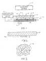
- FIG. 1is a simplified elevation view of a lithographic system in accordance with the present invention
- FIG. 2is a simplified cross-sectional view of a template upon which an imprinting device, shown in FIG. 1 , is formed;
- FIG. 3is a simplified representation of material from which an imprinting layer, shown in FIG. 1 , is comprised before being polymerized and cross-linked;
- FIG. 4is a simplified representation of cross-linked polymer material into which the material shown in FIG. 3 is transformed after being subjected to radiation;
- FIG. 5is a simplified cross-sectional view of a substrate having an imprinted layer formed thereon with the imprint device, shown in FIG. 1 ;
- FIG. 6is a simplified elevation cross-sectional view of the imprint device spaced-apart from the imprint layer, shown in FIG. 1 , after patterning of an imprint layer on a substrate;
- FIG. 7is a detailed view demonstrating the non-planarity of the substrate in accordance with the prior art.
- FIG. 8is a simplified plan view of a template employed to pattern the substrate shown in FIG. 6 in accordance with the present invention.
- FIG. 9is a simplified plan view showing the template, shown in FIG. 8 , imprinting material disposed on the substrate, shown in FIG. 7 ;
- FIG. 10is a simplified plan view showing the various patterns that may be included with the template shown in FIGS. 2 and 8 , in accordance with the present invention.
- FIG. 11is a simplified elevation view of material disposed on a template shown in FIG. 8 , to planarize a substrate in accordance with one embodiment of the present invention
- FIG. 12is a simplified plan view showing the template coupled to a device to apply pressure to one side of the template, in accordance with an alternate embodiment of the present invention
- FIG. 13is a cross-sectional view demonstrating formation of a planarization layer with the template shown in FIG. 8 in accordance with one embodiment of the present invention
- FIG. 14is a cross-sectional view demonstrating formation of a planarization layer with the template shown in FIG. 8 in accordance with an alternate embodiment of the present invention
- FIG. 15is a top down view of the templates shown in FIGS. 2 and 8 in accordance with the present invention.
- FIG. 16is a top down view of the template shown in FIG. 15 in accordance with an alternate embodiment of the present invention.
- a lithographic systemin accordance with an embodiment of the present invention includes a substrate 10 , having a substantially smooth and/or planar region, shown as surface 12 . Disposed opposite substrate 10 is an imprint device 14 having a plurality of features thereon, forming a plurality of spaced-apart recessions 16 and protrusions 18 .
- the recessions 16are a plurality of grooves extending along a direction parallel to protrusions 18 that provide a cross-section of imprint device 14 with a shape of a battlement.
- the recessions 16may correspond to virtually any feature required to create an integrated circuit.
- a translation device 20is connected between imprint device 14 and substrate 10 to vary a distance “d” between imprint device 14 and substrate 10 .
- An exemplary translation deviceis disclosed in U.S. patent application Ser. No. 10/194,414, filed Jul. 11, 2002, entitled “Step and Repeat Imprint Lithography Systems”, assigned to the assignee of the present invention, and which is incorporated by reference herein in its entirety.
- a radiation source 22is located so that imprint device 14 is positioned between radiation source 22 and substrate 10 . Radiation source 22 is configured to impinge radiation on substrate 10 .
- imprint device 14is fabricated from material that allows it to be substantially transparent to the radiation produced by radiation source 22 .
- imprint device 14is a patterning region of a template 15 that typically extends from a surface thereof, forming a mesa of template 15 , shown in FIG. 2 .
- an imprinting layer 24is disposed adjacent to surface 12 , between substrate 10 and imprint device 14 .
- imprinting layer 24may be deposited using any known technique, in the present embodiment, imprinting layer 24 is deposited as a plurality of spaced-apart discrete beads 25 of material 25 a on substrate 10 .
- An exemplary system for depositing materialis disclosed in U.S. patent application Ser. No. 10/191,749, filed Jul. 9, 2002, entitled “System and Method for Dispensing Liquids”, and which is assigned to the assignee of the present invention.
- Imprinting layer 24is formed from a material 25 a that may be selectively polymerized and cross-linked to record a desired pattern. Material 25 a is shown in FIG. 4 as being cross-linked at points 25 b , forming cross-linked polymer material 25 c.
- the pattern recorded by imprinting layer 24is produced, in part, by mechanical contact with imprint device 14 .
- translation mechanism 20reduces the distance “d” to allow imprinting layer 24 to come into mechanical contact with imprint device 14 , spreading beads 25 so as to form imprinting layer 24 with a contiguous formation of material 25 a , shown in FIG. 3 , over surface 12 .
- distance “d”is reduced to allow sub-portions 24 a of imprinting layer 24 to ingress into and fill recessions 16 .
- material 25 ais provided with the requisite viscosity to completely fill recessions 16 in a timely manner, while covering surface with a contiguous formation of material 25 a , on the order of a few milliseconds to a few seconds.
- sub-portions 24 b of imprinting layer 24 in superimposition with protrusions 18remain after the desired, usually minimum distance “d” has been reached, leaving sub-portions 24 a with a thickness t 1 , and sub-portions 24 b with a thickness, t 2 .
- Thicknesses “t 1 ” and “t 2 ”may be any thickness desired, dependent upon the application.
- sub-portions 24 bmay be abrogated entirely whereby the only remaining material from imprinting layer 24 are sub-portions 24 a , after distance, “d” has reached a minimum value. This may occur, for example, when the height of the mesa h m , is substantially greater than the depth, d r , of the recessions 16 .
- radiation source 22produces actinic radiation that polymerizes and cross-links material 25 a , forming cross-linked polymer material 25 c .
- the composition of imprinting layer 24transforms from material 25 a to material 25 c , which is a solid.
- material 25 cis solidified to provide surface 24 c of imprinting layer 24 with a shape conforming to a shape of a surface 14 a of imprint device 14 , shown more clearly in FIG. 6 .
- an exemplary radiation source 22may produce ultraviolet radiation.
- Other radiation sourcesmay be employed, such as thermal, electromagnetic and the like.
- the selection of radiation employed to initiate the polymerization of the material in imprinting layer 24is known to one skilled in the art and typically depends on the specific application which is desired. After imprinting layer 24 is transformed to consist of material 25 c , translation mechanism 20 increases the distance “d” so that imprint device 14 and imprinting layer 24 are spaced-apart.
- additional processingmay be employed to complete the patterning of substrate 10 , for example, etching.
- the material from which imprinting layer 24 is formedmay be varied to define a relative etch rate with respect to substrate 10 , as desired.
- the relative etch rate of imprinting layer 24 to substrate 10may be in a range of about 1.5:1 to about 100:1.
- imprinting layer 24may be provided with an etch differential with respect to photo-resist material (not shown) selectively disposed on surface 24 c .
- the photo-resist material(not shown) may be provided to further pattern imprinting layer 24 , using known techniques.
- Any etch processmay be employed, dependent upon the etch rate desired and the underlying constituents that form substrate 10 and imprinting layer 24 .
- Exemplary etch processesmay include plasma etching, reactive ion etching and the like.
- the aspect ratio of recesses 30 formed from the aforementioned patterning techniquemay be as great as 30:1.
- one embodiment of imprint device 14has recessions 16 defining an aspect ratio in a range of 1:1 to 10:1.
- protrusions 18have a width W 1 in a range of about 10 nm to about 5000 ⁇ m
- recessions 16have a width W 2 in a range of 10 nm to about 5000 ⁇ m.
- imprint device 14may be formed from various conventional materials, such as, but not limited to quartz, fused-silica, silicon, organic polymers, siloxane polymers, borosilicate glass, fluorocarbon polymers, metal, silicon, silicon dioxide, silicon germanium carbon, gallium nitride, silicon germanium, sapphire, gallium arsenide, epitaxial silicon, poly-silicon, gate oxide, indium tin oxide, diamond, and combinations of the above.
- Features of imprint device 14may be formed using any known technique, e.g., machined, wet etch, dry etch and the like.
- a problem addressed by the present inventionconcerns formation of features on substrates having extreme topologies when compared to the dimensions of features formed thereon.
- substrate 110appears to present a non-planar surface 112 .
- Thishas been traditionally found in substrates formed from gallium arsenide (GAs) or indium phosphide (InP).
- Gsgallium arsenide
- InPindium phosphide
- substrates that have historically been considered planarmay present a non-planar surface to features formed thereon.
- substrate 110is shown with variations in surface height.
- the variation in heightfrustrates attempts to control the dimensions of features formed into substrate 110 , because of the resulting differences in distances between surface regions 112 a and 112 b as measured from a backside 112 c of substrate 112 , as h 1 and h 2 , respectively.
- imprint device 14comprises of a conforming template 115 for patterning liquids, such as material 25 a , shown in FIG. 3 , disposed on substrate 110 .
- Template 115includes a body 200 having opposed first 202 and second 204 surfaces.
- First surface 202includes a plurality of recessed regions 206 with a patterning region 208 being disposed between adjacent recessed regions 206 .
- recessed regions 206define flexure regions 210 about which each patterning region 208 may move independent of the remaining patterning regions 208 of template 115 .
- patterning regions 208are areas of surface 204 positioned between adjacent flexure regions 210 .
- template 115compresses material 25 a between surface 204 and surface 112 .
- Recessed regions 206allow flexing of body 200 about the plurality of flexure regions 210 .
- template 115conforms to the profile of surface 112 defined, in part, by the height differential ⁇ h.
- Material 25 amay be disposed on surface 112 and solidified, as described above with respect to FIGS. 1-6 .
- Advantages of conforming template 115is that the same may be employed to create surface 124 c of layer 124 with a substantially smooth profile in the presence of a substrate 110 having an extreme topology.
- patterning regions 208may be provided with recessions 16 and protrusions 18 to define imprint device 14 , shown in FIG. 1 .
- layer 124shown in FIG. 9 may be patterned with recession and protrusions (not shown).
- the pattern provided in patterning regions 208 , shown in FIG. 8 , and imprint device 14 , shown in FIG. 1may be any type of pattern, such as uniform periodic features having common shapes, as well as features having differing shapes.
- recessions 16 and protrusions 18may be arranged on patterning regions 208 , shown in FIG. 8 , to form virtually any desired geometric pattern.
- Exemplary patternsinclude a series of linear grooves/projections 180 , a series of L-Shaped grooves/projections 182 , a series of intersecting grooves/projections defining a matrix 184 , and a series of arcuate grooves/projections 186 , shown in FIG. 10 . Additionally, pillars 188 may project from patterning region 208 and have any cross-sectional shape desired, e.g., circular, polygonal etc.
- template 115may also be employed to form a surface 224 a of layer 224 so as to be smooth and planar.
- the conformality of body 200 to the material 25 a deposited on surface 112is dependent upon many factors, such as the material 25 a from which body 200 is formed and the size of recesses 206 , as well as the volume distribution of material 25 a deposited on surface 112 and the mechanical properties of the same. As a result, for a given body 200 , the conformality of the same is dependent upon the quantity of material 25 a and the mechanical properties of the material 25 a , i.e., viscosity, density and the like.
- the conformality of body 200is dependent upon providing flexure regions 210 with a desired flexing motion. This may be achieved by the selection of material 25 a from which body 200 is formed, as well as the dimensions of recesses 206 in body 200 .
- imprint device 14shown in FIG. 1 , or template 115 may be formed from many differing materials, as discussed above with respect to imprint device 14 .
- a fluid sourcesuch as a pump 250 may be placed in fluid communication with first surface 202 , shown in FIG. 8 , to vary a pressure present.
- a fluid chamber 252includes an inlet 254 and a throughway 256 .
- Template 115is mounted in throughway 256 to substantially restrict fluid flow therethrough.
- template 115 and sides 258 , 260 and 262define a volume 264 .
- Sides 258 , 260 and 262may be more rigid than template 115 .
- template 115may be more sensitive to variations in pressure changes occurring in volume 264 than sides 258 , 260 and 262 .
- pump 250may pressurize or evacuate volume 264 as desired to vary a shape of template 115 to facilitate conformation of template 115 with a surface adjacent to second side 204 .
- the characteristics of material 25 aare important to efficiently pattern substrate 10 in light of the unique deposition process employed.
- material 25 ais deposited on substrate 10 as a plurality of discrete and spaced-apart beads 25 .
- the combined volume of beads 25is such that the material 25 a is distributed appropriately over area of surface 12 where imprinting layer 24 is to be formed.
- imprinting layer 24is spread and patterned concurrently, with the pattern being subsequently set by exposure to radiation, such as ultraviolet radiation.
- material 25 ahave certain characteristics to facilitate rapid and even spreading of material 25 a in beads 25 over surface 12 so that the all thicknesses t 1 are substantially uniform and all thickness t 2 are substantially uniform.
- Exemplary materialsare disclosed in U.S. patent application Ser. No. 10/463,396, filed Jun. 17, 2003, entitled “Method to Reduce Adhesion Between a Conformable Region and a Pattern of a Mold”, and which is incorporated by reference herein in its entirety.
- planarization layer 424provides a smooth and/or planarized surface 424 a upon which to form an additional patterned layer 324 .
- planarization layer 424may be disposed directly upon patterned layer 324 or on a spin-coated layer 324 a that covers patterned layer 324 , shown in FIG. 14 .
- Planarization layer 424may be formed from a number of differing materials, such as, for example, thermoset polymers, thermoplastic polymers, polyepoxies, polyamides, polyurethanes, polycarbonates, polyesters, and combinations thereof. It is desired that planarization layer 424 be formed from material that polymerizes, or cures, in response to the actinic radiation employed to cure imprinting layer 24 , shown in FIG. 1 , and adheres well thereto and other adjacent layers, such as patterned layer 324 shown in FIG. 14 , as well as experience less than 15% shrinkage during curing. It is also desired that planarization layer 424 not substantially penetrate patterned layer 324 .
- planarization layer 424not be swelled by the imprinting layer 24 to the extent where there is more than 5% of imprinting material 25 a , shown in FIG. 3 , penetrating the planarization layer 424 . Additionally, it is desired that the material 25 a have a viscosity of less than 30 cps and more particularly less than 5 cps at 20° C. If spin-on processes are employed to apply planarization layer 424 , the viscosity of the material 25 a from which it is formed may be upwards of 100 cps.
- a class of material that demonstrates desired characteristicsis non-silicon-containing acrylates.
- An exemplary materialis ethylene glycol diacrylate combined with an initiator and stabilizers for long shelf life.
- the initiatormay be any of those discussed above and is responsive to actinic radiation, such as UV light and causes a free radical which facilitates polymerization and cross-linking of the ethylene glycol acrylate.
- the initiatordoes not constitute more than 5% of the mixture.
- An exemplary initiatormay consist of molecules selected from a set consisting of 1-hydroxycyclohexyl phenyl ketone, 2-(2-hydroxypropyl)phenyl ketone, available from Ciba Corporation under the trade name Darocur 1173 and phenylbis(2,4,6-trimethyl benzoyl)phosphine oxide.
- planarization layer 424is fabricated in a manner similar to imprinting layer 24 , shown in FIG. 1 , using a featureless template 115 , shown in FIG. 8 with patterning regions 208 that are smooth and/or planar. In this manner, planarization layer 424 is fabricated to possess a continuous, smooth, relatively defect-free surface that may exhibit excellent adhesion to the patterned layer 324 .
- second surface 204may be treated with a modifying agent.
- a modifying agentis a release layer 34 formed from a fluorocarbon silylating agent.
- Release layer 34 and other surface modifying agentsmay be applied using any known process. For example, processing techniques that may include chemical vapor deposition method, physical vapor deposition, atomic layer deposition or various other techniques, brazing and the like.
- template 15 and 115may have any shape desire, such as the circular shape, shown with respect to substrate 515 , shown in FIG. 15 , or rectangular, shown in FIG. 16 as substrate 616 and may have one patterning region 208 or a plurality of patterning regions 208 arranged as an array, with flexure regions 210 surrounding patterning regions 208 .
- template 15shown in FIG. 2 may have an array of imprinting devices 14 , shown in FIG. 1 , disposed thereon.
- any of the imprinting techniques mentioned abovemay be employed as whole field imprinting process of partial field and may incorporate step and repeat imprinting processes to that end.
- many of the embodiments discussed abovemay be implemented in existing imprint lithography processes that do not employ formation of an imprinting layer by deposition of beads of polymerizable material.
- Exemplary processes in which differing embodiments of the present invention may be employedinclude a hot embossing process disclosed in U.S. Pat. No. 5,772,905, which is incorporated by reference in its entirety herein.
- LADIlaser assisted direct imprinting
Landscapes
- Engineering & Computer Science (AREA)
- Chemical & Material Sciences (AREA)
- Nanotechnology (AREA)
- Physics & Mathematics (AREA)
- General Physics & Mathematics (AREA)
- Crystallography & Structural Chemistry (AREA)
- Manufacturing & Machinery (AREA)
- Condensed Matter Physics & Semiconductors (AREA)
- Mechanical Engineering (AREA)
- Mathematical Physics (AREA)
- Theoretical Computer Science (AREA)
- Shaping Of Tube Ends By Bending Or Straightening (AREA)
- Exposure Of Semiconductors, Excluding Electron Or Ion Beam Exposure (AREA)
Abstract
Description
- The present application claims priority from U.S. provisional patent application No. 60/394,458, filed Jul. 8, 2002, entitled METHOD AND APPARATUS FOR WHOLE WAFER PLANARIZATION USING OPTICAL FLATS AND LIGHT CURABLE LIQUIDS and having Sidlgata V. Sreenivasan, Byung J. Choi and Ronald D. Voisin listed as inventors. The 60/394,458 patent application is incorporated by references in its entirety herein.
- The field of invention relates generally to micro-fabrication of structures. More particularly, the present invention is directed to patterning substrates in furtherance of the formation of structures.
- Micro-fabrication involves the fabrication of very small structures, e.g., having features on the order of micro-meters or smaller. One area in which micro-fabrication has had a sizeable impact is in the processing of integrated circuits. As the semiconductor processing industry continues to strive for larger production yields while increasing the circuits per unit area formed on a substrate, micro-fabrication becomes increasingly important. Micro-fabrication provides greater process control while allowing increased reduction of the minimum feature dimension of the structures formed. Other areas of development in which micro-fabrication has been employed include biotechnology, optical technology, mechanical systems and the like.
- An exemplary micro-fabrication includes forming a relief image in a structure by depositing a polymerizable fluid composition onto a transfer layer. The transfer layer may be a a sacrificial layer providing a mask for patterning the substrate or the substrate itself. A mold makes mechanical contact with the polymerizable fluid. The mold includes a relief structure, and the polymerizable fluid composition fills the relief structure. The polymerizable fluid composition is then subjected to conditions to solidify and polymerize the same, forming a solidified polymeric material on a transfer layer that contains a relief structure complimentary to that of the mold. The mold is then separated from the solid polymeric material such that a replica of the relief structure in the mold is formed in the solidified polymeric material. The solidified polymeric material is subjected to an environment to selectively etch the transfer layer relative to the solidified polymeric material such that a relief image is formed in the transfer layer. With this process, patterns with features on the scale of a few nanometers may be formed. As a result, substrates demonstrate extreme topologies when compared to the dimensions of features formed thereon may prevent accurate reproduction of the pattern in the solidified polymeric layer. Substrates formed from gallium arsenide (GAs) or indium phosphide (InP) have typically been found to demonstrate extreme topologies.
- One manner in which to reduce, if not avoid, the effects of extreme topologies is demonstrated in U.S. Pat. No. 6,334,960 to Willson et al. Willson et al. disclose a method of forming a relief image in a structure that includes providing a substrate having a planarization layer. The planarization layer provides a substantially planar surface upon which a polymerizable fluid composition is deposited. Thereafter, a mold, having a relief structure, makes mechanical contact with the polymerizable fluid composition. The polymerizable fluid composition fills the relief structure. The polymerizable fluid composition is then subjected to conditions to solidify and polymerize the same, forming a solidified polymeric material on the planarization layer that contains a relief structure complimentary to that of the mold. The mold is then separated from the solid polymeric material such that a replica of the relief structure in the mold is formed in the solidified polymeric material. The planarization layer and the solidified polymeric material are subjected to an environment to selectively etch the planarization layer relative to the solidified polymeric material such that the relief image is transferred into the planarization layer.
- It is desired, therefore, to provide improved techniques for pattern substrates having non-planar surfaces employing imprint lithography processes.
- The present invention includes a conforming template for patterning liquids disposed on substrates. The template includes a body having opposed first and second surfaces. The first surface includes a plurality of recessed regions with a patterning region being disposed between adjacent recessed regions. Specifically, the recessed regions define flexure regions about which each patterning region may move independent of the remaining patterning regions of the template. In one embodiment the template is mounted to a fluid chamber having an inlet and a throughway. The template in connected to the throughway and the inlet is connected to a fluid source to facilitate deformation of the template to conform to a profile of a surface adjacent thereto. These and other embodiments are described herein.
FIG. 1 is a simplified elevation view of a lithographic system in accordance with the present invention;FIG. 2 is a simplified cross-sectional view of a template upon which an imprinting device, shown inFIG. 1 , is formed;FIG. 3 is a simplified representation of material from which an imprinting layer, shown inFIG. 1 , is comprised before being polymerized and cross-linked;FIG. 4 is a simplified representation of cross-linked polymer material into which the material shown inFIG. 3 is transformed after being subjected to radiation;FIG. 5 is a simplified cross-sectional view of a substrate having an imprinted layer formed thereon with the imprint device, shown inFIG. 1 ;FIG. 6 is a simplified elevation cross-sectional view of the imprint device spaced-apart from the imprint layer, shown inFIG. 1 , after patterning of an imprint layer on a substrate;FIG. 7 is a detailed view demonstrating the non-planarity of the substrate in accordance with the prior art;FIG. 8 is a simplified plan view of a template employed to pattern the substrate shown inFIG. 6 in accordance with the present invention;FIG. 9 is a simplified plan view showing the template, shown inFIG. 8 , imprinting material disposed on the substrate, shown inFIG. 7 ;FIG. 10 is a simplified plan view showing the various patterns that may be included with the template shown inFIGS. 2 and 8 , in accordance with the present invention;FIG. 11 is a simplified elevation view of material disposed on a template shown inFIG. 8 , to planarize a substrate in accordance with one embodiment of the present invention;FIG. 12 is a simplified plan view showing the template coupled to a device to apply pressure to one side of the template, in accordance with an alternate embodiment of the present invention;FIG. 13 is a cross-sectional view demonstrating formation of a planarization layer with the template shown inFIG. 8 in accordance with one embodiment of the present invention;FIG. 14 is a cross-sectional view demonstrating formation of a planarization layer with the template shown inFIG. 8 in accordance with an alternate embodiment of the present invention;FIG. 15 is a top down view of the templates shown inFIGS. 2 and 8 in accordance with the present invention; andFIG. 16 is a top down view of the template shown inFIG. 15 in accordance with an alternate embodiment of the present invention.- Referring to
FIG. 1 , a lithographic system in accordance with an embodiment of the present invention includes asubstrate 10, having a substantially smooth and/or planar region, shown assurface 12. Disposedopposite substrate 10 is animprint device 14 having a plurality of features thereon, forming a plurality of spaced-apart recessions 16 andprotrusions 18. In the present embodiment, therecessions 16 are a plurality of grooves extending along a direction parallel toprotrusions 18 that provide a cross-section ofimprint device 14 with a shape of a battlement. However, therecessions 16 may correspond to virtually any feature required to create an integrated circuit. Atranslation device 20 is connected betweenimprint device 14 andsubstrate 10 to vary a distance “d” betweenimprint device 14 andsubstrate 10. An exemplary translation device is disclosed in U.S. patent application Ser. No. 10/194,414, filed Jul. 11, 2002, entitled “Step and Repeat Imprint Lithography Systems”, assigned to the assignee of the present invention, and which is incorporated by reference herein in its entirety. Aradiation source 22 is located so thatimprint device 14 is positioned betweenradiation source 22 andsubstrate 10.Radiation source 22 is configured to impinge radiation onsubstrate 10. To realize this,imprint device 14 is fabricated from material that allows it to be substantially transparent to the radiation produced byradiation source 22. Typically,imprint device 14 is a patterning region of atemplate 15 that typically extends from a surface thereof, forming a mesa oftemplate 15, shown inFIG. 2 . - Referring to both
FIGS. 1 and 3 , animprinting layer 24 is disposed adjacent to surface12, betweensubstrate 10 andimprint device 14. Although imprintinglayer 24 may be deposited using any known technique, in the present embodiment,imprinting layer 24 is deposited as a plurality of spaced-apartdiscrete beads 25 ofmaterial 25aonsubstrate 10. An exemplary system for depositing material is disclosed in U.S. patent application Ser. No. 10/191,749, filed Jul. 9, 2002, entitled “System and Method for Dispensing Liquids”, and which is assigned to the assignee of the present invention. Imprintinglayer 24 is formed from a material25athat may be selectively polymerized and cross-linked to record a desired pattern.Material 25ais shown inFIG. 4 as being cross-linked at points25b, formingcross-linked polymer material 25c. - Referring to both
FIGS. 1 and 5 , the pattern recorded by imprintinglayer 24 is produced, in part, by mechanical contact withimprint device 14. To that end,translation mechanism 20 reduces the distance “d” to allowimprinting layer 24 to come into mechanical contact withimprint device 14, spreadingbeads 25 so as to form imprintinglayer 24 with a contiguous formation ofmaterial 25a, shown inFIG. 3 , oversurface 12. In one embodiment, distance “d” is reduced to allow sub-portions24aofimprinting layer 24 to ingress into and fillrecessions 16. - Referring to
FIGS. 1, 3 and5, to facilitate filling ofrecessions 16,material 25ais provided with the requisite viscosity to completely fillrecessions 16 in a timely manner, while covering surface with a contiguous formation ofmaterial 25a, on the order of a few milliseconds to a few seconds. In the present embodiment, sub-portions24bofimprinting layer 24 in superimposition withprotrusions 18 remain after the desired, usually minimum distance “d” has been reached, leaving sub-portions24awith a thickness t1, and sub-portions24bwith a thickness, t2. Thicknesses “t1” and “t2” may be any thickness desired, dependent upon the application. Further, in another embodiment, sub-portions24bmay be abrogated entirely whereby the only remaining material from imprintinglayer 24 are sub-portions24a, after distance, “d” has reached a minimum value. This may occur, for example, when the height of the mesa hm, is substantially greater than the depth, dr, of therecessions 16. - Referring to
FIGS. 1, 3 and4, after a desired distance “d” has been reached,radiation source 22 produces actinic radiation that polymerizes andcross-links material 25a, formingcross-linked polymer material 25c. As a result, the composition ofimprinting layer 24 transforms frommaterial 25atomaterial 25c, which is a solid. Specifically,material 25cis solidified to providesurface 24cofimprinting layer 24 with a shape conforming to a shape of asurface 14aofimprint device 14, shown more clearly inFIG. 6 . - Referring again to
FIGS. 1, 3 and4 anexemplary radiation source 22 may produce ultraviolet radiation. Other radiation sources may be employed, such as thermal, electromagnetic and the like. The selection of radiation employed to initiate the polymerization of the material inimprinting layer 24 is known to one skilled in the art and typically depends on the specific application which is desired. After imprintinglayer 24 is transformed to consist ofmaterial 25c,translation mechanism 20 increases the distance “d” so thatimprint device 14 andimprinting layer 24 are spaced-apart. - Referring to
FIG. 6 , additional processing may be employed to complete the patterning ofsubstrate 10, for example, etching. To facilitate etching, the material from whichimprinting layer 24 is formed may be varied to define a relative etch rate with respect tosubstrate 10, as desired. The relative etch rate ofimprinting layer 24 tosubstrate 10 may be in a range of about 1.5:1 to about 100:1. Alternatively, or in addition to,imprinting layer 24 may be provided with an etch differential with respect to photo-resist material (not shown) selectively disposed onsurface 24c. The photo-resist material (not shown) may be provided to furtherpattern imprinting layer 24, using known techniques. Any etch process may be employed, dependent upon the etch rate desired and the underlying constituents that formsubstrate 10 andimprinting layer 24. Exemplary etch processes may include plasma etching, reactive ion etching and the like. - Referring to
FIGS. 1 and 6 , the aspect ratio ofrecesses 30 formed from the aforementioned patterning technique may be as great as 30:1. To that end, one embodiment ofimprint device 14 hasrecessions 16 defining an aspect ratio in a range of 1:1 to 10:1. Specifically,protrusions 18 have a width W1in a range of about 10 nm to about 5000 μm, andrecessions 16 have a width W2in a range of 10 nm to about 5000 μm. As a result,imprint device 14 may be formed from various conventional materials, such as, but not limited to quartz, fused-silica, silicon, organic polymers, siloxane polymers, borosilicate glass, fluorocarbon polymers, metal, silicon, silicon dioxide, silicon germanium carbon, gallium nitride, silicon germanium, sapphire, gallium arsenide, epitaxial silicon, poly-silicon, gate oxide, indium tin oxide, diamond, and combinations of the above. Features ofimprint device 14 may be formed using any known technique, e.g., machined, wet etch, dry etch and the like. - Referring to
FIG. 7 , a problem addressed by the present invention concerns formation of features on substrates having extreme topologies when compared to the dimensions of features formed thereon. As a result,substrate 110 appears to present anon-planar surface 112. This has been traditionally found in substrates formed from gallium arsenide (GAs) or indium phosphide (InP). However, as the feature dimensions decrease substrates that have historically been considered planar may present a non-planar surface to features formed thereon. For example,substrate 110 is shown with variations in surface height. The variation in height frustrates attempts to control the dimensions of features formed intosubstrate 110, because of the resulting differences in distances between surface regions112aand112bas measured from abackside 112cofsubstrate 112, as h1and h2, respectively. The height differential, Δh, between regions112aand112bis defined as follows:
Δh=|h1−h2| (1)
Height differential, Δh, may be problematic during the imprinting process and/or one or more post imprinting process, e.g., etching. - Referring to
FIGS. 1, 7 and8, to overcome the problems resulting from height differential, Δh,imprint device 14 comprises of a conformingtemplate 115 for patterning liquids, such asmaterial 25a, shown inFIG. 3 , disposed onsubstrate 110.Template 115 includes abody 200 having opposed first202 and second204 surfaces.First surface 202 includes a plurality of recessedregions 206 with apatterning region 208 being disposed between adjacent recessedregions 206. Specifically, recessedregions 206 defineflexure regions 210 about which eachpatterning region 208 may move independent of the remainingpatterning regions 208 oftemplate 115. As shown, patterningregions 208 are areas ofsurface 204 positioned betweenadjacent flexure regions 210. - Referring to both
FIGS. 3, 8 and9, during imprinting ofmaterial 25acontained inlayer 124,template 115 compresses material25abetweensurface 204 andsurface 112. Recessedregions 206 allow flexing ofbody 200 about the plurality offlexure regions 210. In this manner,template 115 conforms to the profile ofsurface 112 defined, in part, by the height differential Δh.Material 25amay be disposed onsurface 112 and solidified, as described above with respect toFIGS. 1-6 . Advantages of conformingtemplate 115 is that the same may be employed to create surface124coflayer 124 with a substantially smooth profile in the presence of asubstrate 110 having an extreme topology. Additionally, one or more ofpatterning regions 208, shown inFIG. 8 , may be provided withrecessions 16 andprotrusions 18 to defineimprint device 14, shown inFIG. 1 . In this manner,layer 124, shown inFIG. 9 may be patterned with recession and protrusions (not shown). It should be noted that the pattern provided inpatterning regions 208, shown inFIG. 8 , andimprint device 14, shown inFIG. 1 , may be any type of pattern, such as uniform periodic features having common shapes, as well as features having differing shapes. Further,recessions 16 andprotrusions 18 may be arranged on patterningregions 208, shown inFIG. 8 , to form virtually any desired geometric pattern. Exemplary patterns include a series of linear grooves/projections 180, a series of L-Shaped grooves/projections 182, a series of intersecting grooves/projections defining amatrix 184, and a series of arcuate grooves/projections 186, shown inFIG. 10 . Additionally,pillars 188 may project from patterningregion 208 and have any cross-sectional shape desired, e.g., circular, polygonal etc. - Referring to
FIGS. 3 and 11 ,template 115 may also be employed to form a surface224aoflayer 224 so as to be smooth and planar. The conformality ofbody 200 to the material25adeposited onsurface 112 is dependent upon many factors, such as the material25afrom whichbody 200 is formed and the size ofrecesses 206, as well as the volume distribution ofmaterial 25adeposited onsurface 112 and the mechanical properties of the same. As a result, for a givenbody 200, the conformality of the same is dependent upon the quantity ofmaterial 25aand the mechanical properties of the material25a, i.e., viscosity, density and the like. For a given volume ofmaterial 25adeposited onsurface 112, the conformality ofbody 200 is dependent upon providingflexure regions 210 with a desired flexing motion. This may be achieved by the selection ofmaterial 25afrom whichbody 200 is formed, as well as the dimensions ofrecesses 206 inbody 200. To that end,imprint device 14, shown inFIG. 1 , ortemplate 115 may be formed from many differing materials, as discussed above with respect toimprint device 14. - Referring to
FIG. 12 , to facilitate conformingtemplate 115 to a surface, a fluid source, such as a pump250 may be placed in fluid communication withfirst surface 202, shown inFIG. 8 , to vary a pressure present. To that end, afluid chamber 252 includes aninlet 254 and athroughway 256.Template 115 is mounted inthroughway 256 to substantially restrict fluid flow therethrough. As aresult template 115 andsides Sides template 115. In this fashion,template 115 may be more sensitive to variations in pressure changes occurring in volume264 thansides template 115 to facilitate conformation oftemplate 115 with a surface adjacent tosecond side 204. - Referring to
FIGS. 1, 3 and6, the characteristics ofmaterial 25aare important to efficientlypattern substrate 10 in light of the unique deposition process employed. As mentioned above,material 25ais deposited onsubstrate 10 as a plurality of discrete and spaced-apartbeads 25. The combined volume ofbeads 25 is such that the material25ais distributed appropriately over area ofsurface 12 whereimprinting layer 24 is to be formed. As a result,imprinting layer 24 is spread and patterned concurrently, with the pattern being subsequently set by exposure to radiation, such as ultraviolet radiation. As a result of the deposition process it is desired thatmaterial 25ahave certain characteristics to facilitate rapid and even spreading ofmaterial 25ainbeads 25 oversurface 12 so that the all thicknesses t1are substantially uniform and all thickness t2are substantially uniform. Exemplary materials are disclosed in U.S. patent application Ser. No. 10/463,396, filed Jun. 17, 2003, entitled “Method to Reduce Adhesion Between a Conformable Region and a Pattern of a Mold”, and which is incorporated by reference herein in its entirety. - Referring to
FIGS. 8 and 13 , employingtemplate 115 for planarization facilitates imprint lithography on patterned layers. For example, assuming a patterned layer324 is present onsubstrate 310,template 115 may be employed to create aplanarization layer 424.Planarization layer 424 provides a smooth and/or planarized surface424aupon which to form an additional patterned layer324. To that end,planarization layer 424 may be disposed directly upon patterned layer324 or on a spin-coated layer324athat covers patterned layer324, shown inFIG. 14 .Planarization layer 424 may be formed from a number of differing materials, such as, for example, thermoset polymers, thermoplastic polymers, polyepoxies, polyamides, polyurethanes, polycarbonates, polyesters, and combinations thereof. It is desired thatplanarization layer 424 be formed from material that polymerizes, or cures, in response to the actinic radiation employed to cureimprinting layer 24, shown inFIG. 1 , and adheres well thereto and other adjacent layers, such as patterned layer324 shown inFIG. 14 , as well as experience less than 15% shrinkage during curing. It is also desired thatplanarization layer 424 not substantially penetrate patterned layer324. Specifically, it is desired thatplanarization layer 424 not be swelled by theimprinting layer 24 to the extent where there is more than 5% of imprintingmaterial 25a, shown inFIG. 3 , penetrating theplanarization layer 424. Additionally, it is desired that the material25ahave a viscosity of less than 30 cps and more particularly less than 5 cps at 20° C. If spin-on processes are employed to applyplanarization layer 424, the viscosity of the material25afrom which it is formed may be upwards of 100 cps. - A class of material that demonstrates desired characteristics is non-silicon-containing acrylates. An exemplary material is ethylene glycol diacrylate combined with an initiator and stabilizers for long shelf life. The initiator, may be any of those discussed above and is responsive to actinic radiation, such as UV light and causes a free radical which facilitates polymerization and cross-linking of the ethylene glycol acrylate. Typically, the initiator does not constitute more than 5% of the mixture. An exemplary initiator may consist of molecules selected from a set consisting of 1-hydroxycyclohexyl phenyl ketone, 2-(2-hydroxypropyl)phenyl ketone, available from Ciba Corporation under the trade name Darocur 1173 and phenylbis(2,4,6-trimethyl benzoyl)phosphine oxide.
- Employing ethylene glycol diacrylate,
planarization layer 424 is fabricated in a manner similar toimprinting layer 24, shown inFIG. 1 , using afeatureless template 115, shown inFIG. 8 withpatterning regions 208 that are smooth and/or planar. In this manner,planarization layer 424 is fabricated to possess a continuous, smooth, relatively defect-free surface that may exhibit excellent adhesion to the patterned layer324. - Referring to
FIGS. 1, 8 and13, to ensure thatplanarization layer 424 does not adhere totemplate 115second surface 204 may be treated with a modifying agent. One such modifying agent is arelease layer 34 formed from a fluorocarbon silylating agent.Release layer 34 and other surface modifying agents may be applied using any known process. For example, processing techniques that may include chemical vapor deposition method, physical vapor deposition, atomic layer deposition or various other techniques, brazing and the like. - Referring to
FIGS. 2 and 8 , it should be understood thattemplate substrate 515, shown inFIG. 15 , or rectangular, shown inFIG. 16 as substrate616 and may have onepatterning region 208 or a plurality ofpatterning regions 208 arranged as an array, withflexure regions 210 surroundingpatterning regions 208. Similarly,template 15, shown inFIG. 2 may have an array ofimprinting devices 14, shown inFIG. 1 , disposed thereon. - The embodiments of the present invention described above are exemplary. Many changes and modifications may be made to the disclosure recited above, while remaining within the scope of the invention. For example, any of the imprinting techniques mentioned above may be employed as whole field imprinting process of partial field and may incorporate step and repeat imprinting processes to that end. Additionally, many of the embodiments discussed above may be implemented in existing imprint lithography processes that do not employ formation of an imprinting layer by deposition of beads of polymerizable material. Exemplary processes in which differing embodiments of the present invention may be employed include a hot embossing process disclosed in U.S. Pat. No. 5,772,905, which is incorporated by reference in its entirety herein. Additionally, many of the embodiments of the present invention may be employed using a laser assisted direct imprinting (LADI) process of the type described by Chou et al. inUltrafast and Direct Imprint of Nanostructures in Silicon, Nature, Col. 417, pp. 835-837, June 2002, as well as traditional spin-on processes. Therefore, the scope of the invention should be determined not with reference to the above description, but instead should be determined with reference to the appended claims along with their full scope of equivalents.
Claims (20)
Priority Applications (4)
| Application Number | Priority Date | Filing Date | Title |
|---|---|---|---|
| US10/614,716US7179079B2 (en) | 2002-07-08 | 2003-07-07 | Conforming template for patterning liquids disposed on substrates |
| US11/669,569US7699598B2 (en) | 2002-07-08 | 2007-01-31 | Conforming template for patterning liquids disposed on substrates |
| US12/717,664US8123514B2 (en) | 2002-07-08 | 2010-03-04 | Conforming template for patterning liquids disposed on substrates |
| US13/073,533US8556616B2 (en) | 2002-07-08 | 2011-03-28 | Template having a varying thickness to facilitate expelling a gas positioned between a substrate and the template |
Applications Claiming Priority (2)
| Application Number | Priority Date | Filing Date | Title |
|---|---|---|---|
| US39445802P | 2002-07-08 | 2002-07-08 | |
| US10/614,716US7179079B2 (en) | 2002-07-08 | 2003-07-07 | Conforming template for patterning liquids disposed on substrates |
Related Child Applications (1)
| Application Number | Title | Priority Date | Filing Date |
|---|---|---|---|
| US11/669,569ContinuationUS7699598B2 (en) | 2002-07-08 | 2007-01-31 | Conforming template for patterning liquids disposed on substrates |
Publications (2)
| Publication Number | Publication Date |
|---|---|
| US20050051698A1true US20050051698A1 (en) | 2005-03-10 |
| US7179079B2 US7179079B2 (en) | 2007-02-20 |
Family
ID=34228281
Family Applications (3)
| Application Number | Title | Priority Date | Filing Date |
|---|---|---|---|
| US10/614,716Expired - Fee RelatedUS7179079B2 (en) | 2002-07-08 | 2003-07-07 | Conforming template for patterning liquids disposed on substrates |
| US11/669,569Expired - LifetimeUS7699598B2 (en) | 2002-07-08 | 2007-01-31 | Conforming template for patterning liquids disposed on substrates |
| US12/717,664ActiveUS8123514B2 (en) | 2002-07-08 | 2010-03-04 | Conforming template for patterning liquids disposed on substrates |
Family Applications After (2)
| Application Number | Title | Priority Date | Filing Date |
|---|---|---|---|
| US11/669,569Expired - LifetimeUS7699598B2 (en) | 2002-07-08 | 2007-01-31 | Conforming template for patterning liquids disposed on substrates |
| US12/717,664ActiveUS8123514B2 (en) | 2002-07-08 | 2010-03-04 | Conforming template for patterning liquids disposed on substrates |
Country Status (1)
| Country | Link |
|---|---|
| US (3) | US7179079B2 (en) |
Cited By (30)
| Publication number | Priority date | Publication date | Assignee | Title |
|---|---|---|---|---|
| US20030205657A1 (en)* | 2002-05-01 | 2003-11-06 | Voisin Ronald D. | Methods of manufacturing a lithography template |
| US20040112862A1 (en)* | 2002-12-12 | 2004-06-17 | Molecular Imprints, Inc. | Planarization composition and method of patterning a substrate using the same |
| US20040163563A1 (en)* | 2000-07-16 | 2004-08-26 | The Board Of Regents, The University Of Texas System | Imprint lithography template having a mold to compensate for material changes of an underlying liquid |
| US20040168613A1 (en)* | 2003-02-27 | 2004-09-02 | Molecular Imprints, Inc. | Composition and method to form a release layer |
| US20040256764A1 (en)* | 2003-06-17 | 2004-12-23 | University Of Texas System Board Of Regents | Method to reduce adhesion between a conformable region and a pattern of a mold |
| US20050064344A1 (en)* | 2003-09-18 | 2005-03-24 | University Of Texas System Board Of Regents | Imprint lithography templates having alignment marks |
| US20050084804A1 (en)* | 2003-10-16 | 2005-04-21 | Molecular Imprints, Inc. | Low surface energy templates |
| US20050098534A1 (en)* | 2003-11-12 | 2005-05-12 | Molecular Imprints, Inc. | Formation of conductive templates employing indium tin oxide |
| US20050160934A1 (en)* | 2004-01-23 | 2005-07-28 | Molecular Imprints, Inc. | Materials and methods for imprint lithography |
| US20050187339A1 (en)* | 2004-02-23 | 2005-08-25 | Molecular Imprints, Inc. | Materials for imprint lithography |
| US20050230882A1 (en)* | 2004-04-19 | 2005-10-20 | Molecular Imprints, Inc. | Method of forming a deep-featured template employed in imprint lithography |
| US20050236360A1 (en)* | 2004-04-27 | 2005-10-27 | Molecular Imprints, Inc. | Compliant hard template for UV imprinting |
| US20050282388A1 (en)* | 2004-06-16 | 2005-12-22 | Yong Chen | Imprinting lithography using the liquid/solid transition of metals and their alloys |
| US20060032437A1 (en)* | 2004-08-13 | 2006-02-16 | Molecular Imprints, Inc. | Moat system for an imprint lithography template |
| US20060062922A1 (en)* | 2004-09-23 | 2006-03-23 | Molecular Imprints, Inc. | Polymerization technique to attenuate oxygen inhibition of solidification of liquids and composition therefor |
| US20060081557A1 (en)* | 2004-10-18 | 2006-04-20 | Molecular Imprints, Inc. | Low-k dielectric functional imprinting materials |
| US20060111454A1 (en)* | 2004-11-24 | 2006-05-25 | Molecular Imprints, Inc. | Composition to reduce adhesion between a conformable region and a mold |
| US20060177535A1 (en)* | 2005-02-04 | 2006-08-10 | Molecular Imprints, Inc. | Imprint lithography template to facilitate control of liquid movement |
| US7136150B2 (en) | 2003-09-25 | 2006-11-14 | Molecular Imprints, Inc. | Imprint lithography template having opaque alignment marks |
| US20060266916A1 (en)* | 2005-05-25 | 2006-11-30 | Molecular Imprints, Inc. | Imprint lithography template having a coating to reflect and/or absorb actinic energy |
| US20070021520A1 (en)* | 2005-07-22 | 2007-01-25 | Molecular Imprints, Inc. | Composition for adhering materials together |
| US20070077763A1 (en)* | 2005-09-30 | 2007-04-05 | Molecular Imprints, Inc. | Deposition technique to planarize a multi-layer structure |
| WO2007126702A1 (en)* | 2006-04-03 | 2007-11-08 | Molecular Imprints, Inc. | System to vary the dimensions of a thin template |
| US20080160129A1 (en)* | 2006-05-11 | 2008-07-03 | Molecular Imprints, Inc. | Template Having a Varying Thickness to Facilitate Expelling a Gas Positioned Between a Substrate and the Template |
| US7785526B2 (en) | 2004-07-20 | 2010-08-31 | Molecular Imprints, Inc. | Imprint alignment method, system, and template |
| US20140367881A1 (en)* | 2011-09-06 | 2014-12-18 | Iq Structures S.R.O. | Method of making a product with a functional relief surface with high resolution |
| US20140367887A1 (en)* | 2011-09-23 | 2014-12-18 | 1366 Technologies, Inc. | Methods and apparati for handling, heating and cooling a substrate upon which a pattern is made by a tool in heat flowable material coating, including substrate transport, tool laydown, tool tensioning and tool retraction |
| CN109923658A (en)* | 2016-11-03 | 2019-06-21 | 分子印记公司 | Substrate loading system |
| US11372328B2 (en)* | 2019-08-19 | 2022-06-28 | Canon Kabushiki Kaisha | Mold, imprinting apparatus, and method for manufacturing article |
| US11402749B2 (en)* | 2019-06-19 | 2022-08-02 | Canon Kabushiki Kaisha | Drop pattern correction for nano-fabrication |
Families Citing this family (37)
| Publication number | Priority date | Publication date | Assignee | Title |
|---|---|---|---|---|
| CN1262883C (en)* | 2000-07-17 | 2006-07-05 | 得克萨斯州大学系统董事会 | Method and system of automatic fluid dispensing for imprint lithography processes |
| US20060005657A1 (en)* | 2004-06-01 | 2006-01-12 | Molecular Imprints, Inc. | Method and system to control movement of a body for nano-scale manufacturing |
| US7179079B2 (en)* | 2002-07-08 | 2007-02-20 | Molecular Imprints, Inc. | Conforming template for patterning liquids disposed on substrates |
| US7641840B2 (en)* | 2002-11-13 | 2010-01-05 | Molecular Imprints, Inc. | Method for expelling gas positioned between a substrate and a mold |
| GB0227902D0 (en)* | 2002-11-29 | 2003-01-08 | Ingenia Holdings Ltd | Template |
| US20070027532A1 (en)* | 2003-12-22 | 2007-02-01 | Xingwu Wang | Medical device |
| US8334967B2 (en)* | 2004-05-28 | 2012-12-18 | Board Of Regents, The University Of Texas System | Substrate support system having a plurality of contact lands |
| US7636999B2 (en) | 2005-01-31 | 2009-12-29 | Molecular Imprints, Inc. | Method of retaining a substrate to a wafer chuck |
| US7635263B2 (en)* | 2005-01-31 | 2009-12-22 | Molecular Imprints, Inc. | Chucking system comprising an array of fluid chambers |
| WO2006133365A2 (en)* | 2005-06-08 | 2006-12-14 | Nanoset, Llc | Medical device |
| US7491049B2 (en)* | 2005-09-30 | 2009-02-17 | Hon Hai Precision Industry Co., Ltd. | Apparatus for hot embossing lithography |
| MY144847A (en)* | 2005-12-08 | 2011-11-30 | Molecular Imprints Inc | Method and system for double-sided patterning of substrates |
| US7670530B2 (en) | 2006-01-20 | 2010-03-02 | Molecular Imprints, Inc. | Patterning substrates employing multiple chucks |
| US8142850B2 (en) | 2006-04-03 | 2012-03-27 | Molecular Imprints, Inc. | Patterning a plurality of fields on a substrate to compensate for differing evaporation times |
| US8215946B2 (en) | 2006-05-18 | 2012-07-10 | Molecular Imprints, Inc. | Imprint lithography system and method |
| JP2010503993A (en) | 2006-09-19 | 2010-02-04 | モレキュラー・インプリンツ・インコーポレーテッド | Improved etching techniques for lift-off patterning |
| US20100215794A1 (en)* | 2007-09-06 | 2010-08-26 | Entire Technology Co., Ltd. | Diffusion film molding tool & manufacturing process thereof |
| US7906274B2 (en)* | 2007-11-21 | 2011-03-15 | Molecular Imprints, Inc. | Method of creating a template employing a lift-off process |
| US8012394B2 (en)* | 2007-12-28 | 2011-09-06 | Molecular Imprints, Inc. | Template pattern density doubling |
| US20090212012A1 (en)* | 2008-02-27 | 2009-08-27 | Molecular Imprints, Inc. | Critical dimension control during template formation |
| US20100015270A1 (en)* | 2008-07-15 | 2010-01-21 | Molecular Imprints, Inc. | Inner cavity system for nano-imprint lithography |
| TW201022017A (en)* | 2008-09-30 | 2010-06-16 | Molecular Imprints Inc | Particle mitigation for imprint lithography |
| US20100095862A1 (en)* | 2008-10-22 | 2010-04-22 | Molecular Imprints, Inc. | Double Sidewall Angle Nano-Imprint Template |
| US8652393B2 (en) | 2008-10-24 | 2014-02-18 | Molecular Imprints, Inc. | Strain and kinetics control during separation phase of imprint process |
| US8877073B2 (en)* | 2008-10-27 | 2014-11-04 | Canon Nanotechnologies, Inc. | Imprint lithography template |
| US8309008B2 (en)* | 2008-10-30 | 2012-11-13 | Molecular Imprints, Inc. | Separation in an imprint lithography process |
| US9122148B2 (en)* | 2008-11-03 | 2015-09-01 | Canon Nanotechnologies, Inc. | Master template replication |
| US8529778B2 (en)* | 2008-11-13 | 2013-09-10 | Molecular Imprints, Inc. | Large area patterning of nano-sized shapes |
| WO2010111307A1 (en)* | 2009-03-23 | 2010-09-30 | Intevac, Inc. | A process for optimization of island to trench ratio in patterned media |
| SG172492A1 (en)* | 2009-12-16 | 2011-07-28 | Choong Whye Kwok | Method and apparatus for making polymeric resin-based optical components via ultra-violet radiation |
| US8366431B2 (en) | 2010-04-13 | 2013-02-05 | Sematech, Inc. | Partial die process for uniform etch loading of imprint wafers |
| KR102046933B1 (en) | 2010-11-05 | 2019-11-20 | 캐논 나노테크놀로지즈 인코퍼레이티드 | Patterning of non-convex shaped nanostructures |
| US9149958B2 (en)* | 2011-11-14 | 2015-10-06 | Massachusetts Institute Of Technology | Stamp for microcontact printing |
| US9946159B2 (en) | 2016-03-29 | 2018-04-17 | The United States Of America As Represented By The Secretary Of The Army | Lithographic fragmentation technology |
| CN109382952B (en)* | 2018-10-25 | 2020-06-05 | 遂宁市金虹机械厂 | A fully automatic energy-saving dripping method |
| US11656546B2 (en) | 2020-02-27 | 2023-05-23 | Canon Kabushiki Kaisha | Exposure apparatus for uniform light intensity and methods of using the same |
| US11443940B2 (en)* | 2020-06-24 | 2022-09-13 | Canon Kabushiki Kaisha | Apparatus for uniform light intensity and methods of using the same |
Citations (94)
| Publication number | Priority date | Publication date | Assignee | Title |
|---|---|---|---|---|
| US2975476A (en)* | 1959-03-02 | 1961-03-21 | John E Burke | Press |
| US3945790A (en)* | 1972-12-08 | 1976-03-23 | Thomson-Csf | Pressing device for manufacturing of storage substrates |
| US4201800A (en)* | 1978-04-28 | 1980-05-06 | International Business Machines Corp. | Hardened photoresist master image mask process |
| US4512848A (en)* | 1984-02-06 | 1985-04-23 | Exxon Research And Engineering Co. | Procedure for fabrication of microstructures over large areas using physical replication |
| US4722878A (en)* | 1984-11-09 | 1988-02-02 | Mitsubishi Denki Kabushiki Kaisha | Photomask material |
| US4723903A (en)* | 1984-06-18 | 1988-02-09 | Hitachi, Ltd. | Stamper for replicating high-density data recording disks |
| US4724222A (en)* | 1986-04-28 | 1988-02-09 | American Telephone And Telegraph Company, At&T Bell Laboratories | Wafer chuck comprising a curved reference surface |
| US4731155A (en)* | 1987-04-15 | 1988-03-15 | General Electric Company | Process for forming a lithographic mask |
| US4959252A (en)* | 1986-09-29 | 1990-09-25 | Rhone-Poulenc Chimie | Highly oriented thermotropic optical disc member |
| US5028366A (en)* | 1988-01-12 | 1991-07-02 | Air Products And Chemicals, Inc. | Water based mold release compositions for making molded polyurethane foam |
| US5110514A (en)* | 1989-05-01 | 1992-05-05 | Soane Technologies, Inc. | Controlled casting of a shrinkable material |
| US5206983A (en)* | 1991-06-24 | 1993-05-04 | Wisconsin Alumni Research Foundation | Method of manufacturing micromechanical devices |
| US5240550A (en)* | 1990-09-21 | 1993-08-31 | U.S. Philips Corp. | Method of forming at least one groove in a substrate layer |
| US5348616A (en)* | 1993-05-03 | 1994-09-20 | Motorola, Inc. | Method for patterning a mold |
| US5425848A (en)* | 1993-03-16 | 1995-06-20 | U.S. Philips Corporation | Method of providing a patterned relief of cured photoresist on a flat substrate surface and device for carrying out such a method |
| US5480047A (en)* | 1993-06-04 | 1996-01-02 | Sharp Kabushiki Kaisha | Method for forming a fine resist pattern |
| US5508527A (en)* | 1992-01-31 | 1996-04-16 | Canon Kabushiki Kaisha | Method of detecting positional displacement between mask and wafer, and exposure apparatus adopting the method |
| US5512131A (en)* | 1993-10-04 | 1996-04-30 | President And Fellows Of Harvard College | Formation of microstamped patterns on surfaces and derivative articles |
| US5545367A (en)* | 1992-04-15 | 1996-08-13 | Soane Technologies, Inc. | Rapid prototype three dimensional stereolithography |
| US5601641A (en)* | 1992-07-21 | 1997-02-11 | Tse Industries, Inc. | Mold release composition with polybutadiene and method of coating a mold core |
| US5669303A (en)* | 1996-03-04 | 1997-09-23 | Motorola | Apparatus and method for stamping a surface |
| US5726548A (en)* | 1992-12-18 | 1998-03-10 | Canon Kabushiki Kaisha | Moving stage apparatus and system using the same |
| US5772905A (en)* | 1995-11-15 | 1998-06-30 | Regents Of The University Of Minnesota | Nanoimprint lithography |
| US5776748A (en)* | 1993-10-04 | 1998-07-07 | President And Fellows Of Harvard College | Method of formation of microstamped patterns on plates for adhesion of cells and other biological materials, devices and uses therefor |
| US5785918A (en)* | 1984-08-08 | 1998-07-28 | Seagate Technology, Inc. | Method and apparatus for production of three-dimensional objects by stereolithography |
| US5804017A (en)* | 1995-07-27 | 1998-09-08 | Imation Corp. | Method and apparatus for making an optical information record |
| US5876550A (en)* | 1988-10-05 | 1999-03-02 | Helisys, Inc. | Laminated object manufacturing apparatus and method |
| US5888650A (en)* | 1996-06-03 | 1999-03-30 | Minnesota Mining And Manufacturing Company | Temperature-responsive adhesive article |
| US5900160A (en)* | 1993-10-04 | 1999-05-04 | President And Fellows Of Harvard College | Methods of etching articles via microcontact printing |
| US5937758A (en)* | 1997-11-26 | 1999-08-17 | Motorola, Inc. | Micro-contact printing stamp |
| US5948470A (en)* | 1997-04-28 | 1999-09-07 | Harrison; Christopher | Method of nanoscale patterning and products made thereby |
| US5952127A (en)* | 1991-08-22 | 1999-09-14 | Nec Corporation | Method of fabricating a phase shifting reticle |
| US5956216A (en)* | 1995-05-24 | 1999-09-21 | Regents Of The University Of Minnesota | Magnetic storage having discrete elements with quantized magnetic moments |
| US6039897A (en)* | 1996-08-28 | 2000-03-21 | University Of Washington | Multiple patterned structures on a single substrate fabricated by elastomeric micro-molding techniques |
| US6046056A (en)* | 1996-06-28 | 2000-04-04 | Caliper Technologies Corporation | High throughput screening assay systems in microscale fluidic devices |
| US6051345A (en)* | 1998-04-27 | 2000-04-18 | United Microelectronics Corp. | Method of producing phase shifting mask |
| US6074827A (en)* | 1996-07-30 | 2000-06-13 | Aclara Biosciences, Inc. | Microfluidic method for nucleic acid purification and processing |
| US6117708A (en)* | 1998-02-05 | 2000-09-12 | Micron Technology, Inc. | Use of residual organic compounds to facilitate gate break on a carrier substrate for a semiconductor device |
| US6190929B1 (en)* | 1999-07-23 | 2001-02-20 | Micron Technology, Inc. | Methods of forming semiconductor devices and methods of forming field emission displays |
| US6218316B1 (en)* | 1998-10-22 | 2001-04-17 | Micron Technology, Inc. | Planarization of non-planar surfaces in device fabrication |
| US6251207B1 (en)* | 1998-12-31 | 2001-06-26 | Kimberly-Clark Worldwide, Inc. | Embossing and laminating irregular bonding patterns |
| US6261469B1 (en)* | 1998-10-13 | 2001-07-17 | Honeywell International Inc. | Three dimensionally periodic structural assemblies on nanometer and longer scales |
| US6274294B1 (en)* | 1999-02-03 | 2001-08-14 | Electroformed Stents, Inc. | Cylindrical photolithography exposure process and apparatus |
| US6334960B1 (en)* | 1999-03-11 | 2002-01-01 | Board Of Regents, The University Of Texas System | Step and flash imprint lithography |
| US6355198B1 (en)* | 1996-03-15 | 2002-03-12 | President And Fellows Of Harvard College | Method of forming articles including waveguides via capillary micromolding and microtransfer molding |
| US20020042027A1 (en)* | 1998-10-09 | 2002-04-11 | Chou Stephen Y. | Microscale patterning and articles formed thereby |
| US6377178B1 (en)* | 2000-06-20 | 2002-04-23 | William DeToro | Therapeutic ankle & foot apparatus having a contact sensor mechanism |
| US6387787B1 (en)* | 2001-03-02 | 2002-05-14 | Motorola, Inc. | Lithographic template and method of formation and use |
| US6391217B2 (en)* | 1999-12-23 | 2002-05-21 | University Of Massachusetts | Methods and apparatus for forming submicron patterns on films |
| US6399406B2 (en)* | 2000-06-19 | 2002-06-04 | International Business Machines Corporation | Encapsulated MEMS band-pass filter for integrated circuits and method of fabrication thereof |
| US20020069525A1 (en)* | 2000-09-18 | 2002-06-13 | Junichi Hada | Apparatus and method for mounting components on substrate |
| US6517977B2 (en)* | 2001-03-28 | 2003-02-11 | Motorola, Inc. | Lithographic template and method of formation and use |
| US6518168B1 (en)* | 1995-08-18 | 2003-02-11 | President And Fellows Of Harvard College | Self-assembled monolayer directed patterning of surfaces |
| US6518189B1 (en)* | 1995-11-15 | 2003-02-11 | Regents Of The University Of Minnesota | Method and apparatus for high density nanostructures |
| US6517995B1 (en)* | 1999-09-14 | 2003-02-11 | Massachusetts Institute Of Technology | Fabrication of finely featured devices by liquid embossing |
| US20030034329A1 (en)* | 1998-06-30 | 2003-02-20 | Chou Stephen Y. | Lithographic method for molding pattern with nanoscale depth |
| US20030062334A1 (en)* | 2001-09-25 | 2003-04-03 | Lee Hong Hie | Method for forming a micro-pattern on a substrate by using capillary force |
| US20030080472A1 (en)* | 2001-10-29 | 2003-05-01 | Chou Stephen Y. | Lithographic method with bonded release layer for molding small patterns |
| US20030099736A1 (en)* | 2001-10-25 | 2003-05-29 | Yumiko Anzai | Recording medium and manufacturing method for the same |
| US20030113638A1 (en)* | 2001-12-18 | 2003-06-19 | Mancini David P. | Lithographic template and method of formation and use |
| US6605849B1 (en)* | 2002-02-14 | 2003-08-12 | Symmetricom, Inc. | MEMS analog frequency divider |
| US6607173B2 (en)* | 1998-09-03 | 2003-08-19 | Micron Technology, Inc. | Film on a surface of a mold used during semiconductor device fabrication |
| US20040022888A1 (en)* | 2002-08-01 | 2004-02-05 | Sreenivasan Sidlgata V. | Alignment systems for imprint lithography |
| US20040021866A1 (en)* | 2002-08-01 | 2004-02-05 | Watts Michael P.C. | Scatterometry alignment for imprint lithography |
| US6696220B2 (en)* | 2000-10-12 | 2004-02-24 | Board Of Regents, The University Of Texas System | Template for room temperature, low pressure micro-and nano-imprint lithography |
| US20040036201A1 (en)* | 2000-07-18 | 2004-02-26 | Princeton University | Methods and apparatus of field-induced pressure imprint lithography |
| US20040046288A1 (en)* | 2000-07-18 | 2004-03-11 | Chou Stephen Y. | Laset assisted direct imprint lithography |
| US6716754B2 (en)* | 2002-03-12 | 2004-04-06 | Micron Technology, Inc. | Methods of forming patterns and molds for semiconductor constructions |
| US6743368B2 (en)* | 2002-01-31 | 2004-06-01 | Hewlett-Packard Development Company, L.P. | Nano-size imprinting stamp using spacer technique |
| US20040110856A1 (en)* | 2002-12-04 | 2004-06-10 | Young Jung Gun | Polymer solution for nanoimprint lithography to reduce imprint temperature and pressure |
| US6753131B1 (en)* | 1996-07-22 | 2004-06-22 | President And Fellows Of Harvard College | Transparent elastomeric, contact-mode photolithography mask, sensor, and wavefront engineering element |
| US20040124566A1 (en)* | 2002-07-11 | 2004-07-01 | Sreenivasan Sidlgata V. | Step and repeat imprint lithography processes |
| US20040131718A1 (en)* | 2000-07-18 | 2004-07-08 | Princeton University | Lithographic apparatus for fluid pressure imprint lithography |
| US20040137734A1 (en)* | 1995-11-15 | 2004-07-15 | Princeton University | Compositions and processes for nanoimprinting |
| US20040150129A1 (en)* | 2002-04-22 | 2004-08-05 | International Business Machines Corporation | Process of fabricating a precision microcontact printing stamp |
| US20040156108A1 (en)* | 2001-10-29 | 2004-08-12 | Chou Stephen Y. | Articles comprising nanoscale patterns with reduced edge roughness and methods of making same |
| US6776094B1 (en)* | 1993-10-04 | 2004-08-17 | President & Fellows Of Harvard College | Kit For Microcontact Printing |
| US20040163563A1 (en)* | 2000-07-16 | 2004-08-26 | The Board Of Regents, The University Of Texas System | Imprint lithography template having a mold to compensate for material changes of an underlying liquid |
| US6849558B2 (en)* | 2002-05-22 | 2005-02-01 | The Board Of Trustees Of The Leland Stanford Junior University | Replication and transfer of microstructures and nanostructures |
| US20050037143A1 (en)* | 2000-07-18 | 2005-02-17 | Chou Stephen Y. | Imprint lithography with improved monitoring and control and apparatus therefor |
| US20050051742A1 (en)* | 1995-02-01 | 2005-03-10 | Nikon Corporation | Method of detecting position of mark on substrate, position detection apparatus using this method, and exposure apparatus using this position detection apparatus |
| US20050064344A1 (en)* | 2003-09-18 | 2005-03-24 | University Of Texas System Board Of Regents | Imprint lithography templates having alignment marks |
| US20050067379A1 (en)* | 2003-09-25 | 2005-03-31 | Molecular Imprints, Inc. | Imprint lithography template having opaque alignment marks |
| US20050084804A1 (en)* | 2003-10-16 | 2005-04-21 | Molecular Imprints, Inc. | Low surface energy templates |
| US20050100830A1 (en)* | 2003-10-27 | 2005-05-12 | Molecular Imprints, Inc. | Methods for fabricating patterned features utilizing imprint lithography |
| US20050098534A1 (en)* | 2003-11-12 | 2005-05-12 | Molecular Imprints, Inc. | Formation of conductive templates employing indium tin oxide |
| US6900881B2 (en)* | 2002-07-11 | 2005-05-31 | Molecular Imprints, Inc. | Step and repeat imprint lithography systems |
| US6908861B2 (en)* | 2002-07-11 | 2005-06-21 | Molecular Imprints, Inc. | Method for imprint lithography using an electric field |
| US6916684B2 (en)* | 2003-03-18 | 2005-07-12 | Delphi Technologies, Inc. | Wafer-applied underfill process |
| US20050158637A1 (en)* | 2004-01-15 | 2005-07-21 | Samsung Electronics Co., Ltd. | Template, method of forming the template and method of forming a pattern on a semiconductor device using the template |
| US6932934B2 (en)* | 2002-07-11 | 2005-08-23 | Molecular Imprints, Inc. | Formation of discontinuous films during an imprint lithography process |
| US20060019183A1 (en)* | 2004-07-20 | 2006-01-26 | Molecular Imprints, Inc. | Imprint alignment method, system, and template |
| US7037639B2 (en)* | 2002-05-01 | 2006-05-02 | Molecular Imprints, Inc. | Methods of manufacturing a lithography template |
| US20060096949A1 (en)* | 2004-04-27 | 2006-05-11 | Molecular Imprints, Inc. | Method of forming a compliant template for UV imprinting |
Family Cites Families (91)
| Publication number | Priority date | Publication date | Assignee | Title |
|---|---|---|---|---|
| GB494877A (en) | 1938-03-01 | 1938-11-02 | Johnson Bros Hanley Ltd | Improvements in or relating to pottery ware and the manufacture thereof |
| US3130412A (en)* | 1959-07-31 | 1964-04-21 | Scott Paper Co | Process of and apparatus for treating sheet materials and product |
| GB1139808A (en) | 1965-05-11 | 1969-01-15 | Hayes Engineers Leeds Ltd | Improvements in or relating to tracer valve control units |
| GB1146618A (en) | 1965-10-11 | 1969-03-26 | Harry Frank Gipe | Method for preparing photo-lithographic plates |
| US3577593A (en) | 1968-10-29 | 1971-05-04 | Bird & Son | Apparatus for heat and vacuum-pressure machine molding |
| US3946367A (en)* | 1972-12-20 | 1976-03-23 | Videonics Of Hawaii, Inc. | Three dimensional electro-optical retrieval system |
| FR2339741A1 (en)* | 1976-01-30 | 1977-08-26 | Snecma | ABRADABLE STATOR GASKET FOR AXIAL TURBOMACHINE AND ITS EXECUTION PROCESS |
| DE2800476A1 (en) | 1977-01-07 | 1978-07-13 | Instruments Sa | Mass prodn. method for grids, graticules etc. - using revolving drum, belt carrying resin and UV light source for polymerisation process |
| NL177721B (en)* | 1977-03-14 | 1985-06-03 | Philips Nv | METHOD FOR MANUFACTURING A PLASTIC INFORMATION CARRIER WITH LAYERED STRUCTURE AND AN APPARATUS FOR CARRYING OUT THE METHOD |
| NL7906117A (en)* | 1979-08-10 | 1981-02-12 | Philips Nv | METHOD AND APPARATUS FOR MANUFACTURING A PLASTIC INFORMATION CARRIER |
| JPS5820046U (en) | 1981-07-31 | 1983-02-07 | 東陶機器株式会社 | Mounting device between ceiling wall and side wall in sanitary equipment room |
| JPS5884808A (en) | 1981-11-13 | 1983-05-21 | Nippon Synthetic Chem Ind Co Ltd:The | Preparation of resinous material |
| US4601861A (en)* | 1982-09-30 | 1986-07-22 | Amerace Corporation | Methods and apparatus for embossing a precision optical pattern in a resinous sheet or laminate |
| US4514249A (en)* | 1984-07-19 | 1985-04-30 | Brown & Williamson Tobacco Corporation | Device for making grooves in cigarette filters |
| EP0245461A1 (en) | 1985-11-18 | 1987-11-19 | EASTMAN KODAK COMPANY (a New Jersey corporation) | Process for making optical recording media |
| DE3719200A1 (en)* | 1987-06-09 | 1988-12-29 | Ibm Deutschland | OPTICAL DISK AND METHOD FOR THEIR PRODUCTION |
| JPH01196749A (en) | 1988-01-30 | 1989-08-08 | Hoya Corp | Manufacture of substrate for optical information recording medium |
| JPH0292603A (en) | 1988-09-30 | 1990-04-03 | Hoya Corp | Manufacture of data recording board with guide groove |
| US5171490A (en) | 1988-11-29 | 1992-12-15 | Fudim Efrem V | Method and apparatus for production of three-dimensional objects by irradiation of photopolymers |
| JPH02192045A (en) | 1989-01-20 | 1990-07-27 | Fujitsu Ltd | Production of optical disk substrate |
| JPH0781024B2 (en) | 1989-03-22 | 1995-08-30 | 旭硝子株式会社 | Water repellency. Antifouling transparent base material and structure equipped with the same |
| JPH0390345U (en) | 1989-12-28 | 1991-09-13 | ||
| US5016691A (en) | 1990-06-19 | 1991-05-21 | Lucien Bernier | Apparatus for centering template guide on router |
| JPH0580530A (en) | 1991-09-24 | 1993-04-02 | Hitachi Ltd | Production of thin film pattern |
| US6153886A (en) | 1993-02-19 | 2000-11-28 | Nikon Corporation | Alignment apparatus in projection exposure apparatus |
| US5464711A (en) | 1994-08-01 | 1995-11-07 | Motorola Inc. | Process for fabricating an X-ray absorbing mask |
| US5477058A (en) | 1994-11-09 | 1995-12-19 | Kabushiki Kaisha Toshiba | Attenuated phase-shifting mask with opaque reticle alignment marks |
| KR960025390A (en)* | 1994-12-03 | 1996-07-20 | 안시환 | Manufacturing method of optical disk stamper |
| US5708652A (en)* | 1995-02-28 | 1998-01-13 | Sony Corporation | Multi-layer recording medium and method for producing same |
| US5849209A (en) | 1995-03-31 | 1998-12-15 | Johnson & Johnson Vision Products, Inc. | Mold material made with additives |
| GB9509487D0 (en) | 1995-05-10 | 1995-07-05 | Ici Plc | Micro relief element & preparation thereof |
| JP3298607B2 (en)* | 1995-09-29 | 2002-07-02 | ソニー株式会社 | Liquid crystal element and manufacturing method thereof |
| US5849222A (en) | 1995-09-29 | 1998-12-15 | Johnson & Johnson Vision Products, Inc. | Method for reducing lens hole defects in production of contact lens blanks |
| US6482742B1 (en) | 2000-07-18 | 2002-11-19 | Stephen Y. Chou | Fluid pressure imprint lithography |
| US5817376A (en) | 1996-03-26 | 1998-10-06 | Minnesota Mining And Manufacturing Company | Free-radically polymerizable compositions capable of being coated by electrostatic assistance |
| JPH09278490A (en) | 1996-04-11 | 1997-10-28 | Matsushita Electric Ind Co Ltd | Water repellent glass coat and method for producing the same |
| US5853446A (en) | 1996-04-16 | 1998-12-29 | Corning Incorporated | Method for forming glass rib structures |
| US6368752B1 (en) | 1996-10-29 | 2002-04-09 | Motorola, Inc. | Low stress hard mask formation method during refractory radiation mask fabrication |
| US5885514A (en) | 1996-12-09 | 1999-03-23 | Dana Corporation | Ambient UVL-curable elastomer mold apparatus |
| AU3818997A (en) | 1997-07-25 | 1999-02-16 | Regents Of The University Of Minnesota | Single-electron floating-gate mos memory |
| IT1294942B1 (en)* | 1997-08-01 | 1999-04-23 | Sacmi | PROCESS OF PRESSING CERAMIC POWDERS AND EQUIPMENT FOR IMPLEMENTING THE SAME. |
| JP3780700B2 (en) | 1998-05-26 | 2006-05-31 | セイコーエプソン株式会社 | Pattern forming method, pattern forming apparatus, pattern forming plate, pattern forming plate manufacturing method, color filter manufacturing method, conductive film manufacturing method, and liquid crystal panel manufacturing method |
| DE19832414C2 (en) | 1998-07-18 | 2000-07-20 | Rob Borgmann | Screen printing method for printing flat objects, in particular glass panes, with a decor and device for carrying out the method |
| WO2000021689A1 (en) | 1998-10-09 | 2000-04-20 | The Trustees Of Princeton University | Microscale patterning and articles formed thereby |
| US6248486B1 (en) | 1998-11-23 | 2001-06-19 | U.S. Philips Corporation | Method of detecting aberrations of an optical imaging system |
| US6780001B2 (en) | 1999-07-30 | 2004-08-24 | Formfactor, Inc. | Forming tool for forming a contoured microelectronic spring mold |
| US6165911A (en) | 1999-12-29 | 2000-12-26 | Calveley; Peter Braden | Method of patterning a metal layer |
| SE515962C2 (en) | 2000-03-15 | 2001-11-05 | Obducat Ab | Device for transferring patterns to objects |
| SE0001367L (en) | 2000-04-13 | 2001-10-14 | Obducat Ab | Apparatus and method for electrochemical processing of substrates |
| SE516414C2 (en) | 2000-05-24 | 2002-01-15 | Obducat Ab | Method of producing a template, as well as the template made from it |
| US20020159918A1 (en) | 2000-06-25 | 2002-10-31 | Fan-Gang Tseng | Micro-fabricated stamp array for depositing biologic diagnostic testing samples on bio-bindable surface |
| US6326627B1 (en) | 2000-08-02 | 2001-12-04 | Archimedes Technology Group, Inc. | Mass filtering sputtered ion source |
| WO2002022916A1 (en) | 2000-09-18 | 2002-03-21 | Obducat Aktiebolag | Method of etching, as well as frame element, mask and prefabricated substrate element for use in such etching |
| US6783719B2 (en) | 2001-01-19 | 2004-08-31 | Korry Electronics, Co. | Mold with metal oxide surface compatible with ionic release agents |
| JP2002299226A (en) | 2001-04-03 | 2002-10-11 | Nikon Corp | Stencil mask for electron beam exposure and method of manufacturing the same |
| US6664026B2 (en) | 2001-03-22 | 2003-12-16 | International Business Machines Corporation | Method of manufacturing high aspect ratio photolithographic features |
| US6963947B2 (en)* | 2001-05-08 | 2005-11-08 | Tao Logic Systems Llc | Driver supporting bridge method and apparatus |
| JP2002353102A (en) | 2001-05-23 | 2002-12-06 | Hitachi Ltd | Method for manufacturing semiconductor device |
| SG169225A1 (en) | 2001-07-25 | 2011-03-30 | Univ Princeton | Nanochannel arrays and their preparation and use for high throughput macromolecular analysis |
| DE10307518B4 (en) | 2002-02-22 | 2011-04-14 | Hoya Corp. | Halftone phase shift mask blank, halftone phase shift mask and method of making the same |
| TW594431B (en) | 2002-03-01 | 2004-06-21 | Asml Netherlands Bv | Calibration methods, calibration substrates, lithographic apparatus and device manufacturing methods |
| AU2003230676A1 (en) | 2002-03-15 | 2003-09-29 | Princeton University | Laser assisted direct imprint lithography |
| CA2380114C (en)* | 2002-04-04 | 2010-01-19 | Obducat Aktiebolag | Imprint method and device |
| CN1678443B (en) | 2002-05-24 | 2012-12-19 | 斯蒂文·Y·周 | Method and apparatus for field pressure-sensitive imprint lithography |
| US6852454B2 (en) | 2002-06-18 | 2005-02-08 | Freescale Semiconductor, Inc. | Multi-tiered lithographic template and method of formation and use |
| US7179079B2 (en) | 2002-07-08 | 2007-02-20 | Molecular Imprints, Inc. | Conforming template for patterning liquids disposed on substrates |
| MY164487A (en) | 2002-07-11 | 2017-12-29 | Molecular Imprints Inc | Step and repeat imprint lithography processes |
| US6916584B2 (en) | 2002-08-01 | 2005-07-12 | Molecular Imprints, Inc. | Alignment methods for imprint lithography |
| WO2004013693A2 (en) | 2002-08-01 | 2004-02-12 | Molecular Imprints, Inc. | Scatterometry alignment for imprint lithography |
| US8349241B2 (en)* | 2002-10-04 | 2013-01-08 | Molecular Imprints, Inc. | Method to arrange features on a substrate to replicate features having minimal dimensional variability |
| EP1460738A3 (en) | 2003-03-21 | 2004-09-29 | Avalon Photonics AG | Wafer-scale replication-technique for opto-mechanical structures on opto-electronic devices |
| US6943117B2 (en) | 2003-03-27 | 2005-09-13 | Korea Institute Of Machinery & Materials | UV nanoimprint lithography process using elementwise embossed stamp and selectively additive pressurization |
| US20040202865A1 (en) | 2003-04-08 | 2004-10-14 | Andrew Homola | Release coating for stamper |
| US6808646B1 (en) | 2003-04-29 | 2004-10-26 | Hewlett-Packard Development Company, L.P. | Method of replicating a high resolution three-dimensional imprint pattern on a compliant media of arbitrary size |
| US7070406B2 (en) | 2003-04-29 | 2006-07-04 | Hewlett-Packard Development Company, L.P. | Apparatus for embossing a flexible substrate with a pattern carried by an optically transparent compliant media |
| TW570290U (en)* | 2003-05-02 | 2004-01-01 | Ind Tech Res Inst | Uniform pressing device for nanometer transfer-print |
| WO2004114016A2 (en) | 2003-06-09 | 2004-12-29 | Princeton University Office Of Technology Licensing And Intellectual Property | Imprint lithography with improved monitoring and control and apparatus therefor |
| TWI228638B (en) | 2003-06-10 | 2005-03-01 | Ind Tech Res Inst | Method for and apparatus for bonding patterned imprint to a substrate by adhering means |
| KR100558754B1 (en) | 2004-02-24 | 2006-03-10 | 한국기계연구원 | UV nanoimprint lithography process and apparatus performing the process |
| US20050189676A1 (en)* | 2004-02-27 | 2005-09-01 | Molecular Imprints, Inc. | Full-wafer or large area imprinting with multiple separated sub-fields for high throughput lithography |
| US20050230882A1 (en)* | 2004-04-19 | 2005-10-20 | Molecular Imprints, Inc. | Method of forming a deep-featured template employed in imprint lithography |
| US20050276919A1 (en)* | 2004-06-01 | 2005-12-15 | Molecular Imprints, Inc. | Method for dispensing a fluid on a substrate |
| US7309225B2 (en) | 2004-08-13 | 2007-12-18 | Molecular Imprints, Inc. | Moat system for an imprint lithography template |
| WO2006060757A2 (en)* | 2004-12-01 | 2006-06-08 | Molecular Imprints, Inc. | Eliminating printability of sub-resolution defects in imprint lithography |
| US7798801B2 (en) | 2005-01-31 | 2010-09-21 | Molecular Imprints, Inc. | Chucking system for nano-manufacturing |
| US20060177535A1 (en) | 2005-02-04 | 2006-08-10 | Molecular Imprints, Inc. | Imprint lithography template to facilitate control of liquid movement |
| US20060266916A1 (en) | 2005-05-25 | 2006-11-30 | Molecular Imprints, Inc. | Imprint lithography template having a coating to reflect and/or absorb actinic energy |
| US8001924B2 (en)* | 2006-03-31 | 2011-08-23 | Asml Netherlands B.V. | Imprint lithography |
| TW200801794A (en)* | 2006-04-03 | 2008-01-01 | Molecular Imprints Inc | Method of concurrently patterning a substrate having a plurality of fields and a plurality of alignment marks |
| US8142850B2 (en)* | 2006-04-03 | 2012-03-27 | Molecular Imprints, Inc. | Patterning a plurality of fields on a substrate to compensate for differing evaporation times |
| JP4819577B2 (en)* | 2006-05-31 | 2011-11-24 | キヤノン株式会社 | Pattern transfer method and pattern transfer apparatus |
- 2003
- 2003-07-07USUS10/614,716patent/US7179079B2/ennot_activeExpired - Fee Related
- 2007
- 2007-01-31USUS11/669,569patent/US7699598B2/ennot_activeExpired - Lifetime
- 2010
- 2010-03-04USUS12/717,664patent/US8123514B2/enactiveActive
Patent Citations (99)
| Publication number | Priority date | Publication date | Assignee | Title |
|---|---|---|---|---|
| US2975476A (en)* | 1959-03-02 | 1961-03-21 | John E Burke | Press |
| US3945790A (en)* | 1972-12-08 | 1976-03-23 | Thomson-Csf | Pressing device for manufacturing of storage substrates |
| US4201800A (en)* | 1978-04-28 | 1980-05-06 | International Business Machines Corp. | Hardened photoresist master image mask process |
| US4512848A (en)* | 1984-02-06 | 1985-04-23 | Exxon Research And Engineering Co. | Procedure for fabrication of microstructures over large areas using physical replication |
| US4723903A (en)* | 1984-06-18 | 1988-02-09 | Hitachi, Ltd. | Stamper for replicating high-density data recording disks |
| US5785918A (en)* | 1984-08-08 | 1998-07-28 | Seagate Technology, Inc. | Method and apparatus for production of three-dimensional objects by stereolithography |
| US4722878A (en)* | 1984-11-09 | 1988-02-02 | Mitsubishi Denki Kabushiki Kaisha | Photomask material |
| US4724222A (en)* | 1986-04-28 | 1988-02-09 | American Telephone And Telegraph Company, At&T Bell Laboratories | Wafer chuck comprising a curved reference surface |
| US4959252A (en)* | 1986-09-29 | 1990-09-25 | Rhone-Poulenc Chimie | Highly oriented thermotropic optical disc member |
| US4731155A (en)* | 1987-04-15 | 1988-03-15 | General Electric Company | Process for forming a lithographic mask |
| US5028366A (en)* | 1988-01-12 | 1991-07-02 | Air Products And Chemicals, Inc. | Water based mold release compositions for making molded polyurethane foam |
| US5876550A (en)* | 1988-10-05 | 1999-03-02 | Helisys, Inc. | Laminated object manufacturing apparatus and method |
| US5110514A (en)* | 1989-05-01 | 1992-05-05 | Soane Technologies, Inc. | Controlled casting of a shrinkable material |
| US5240550A (en)* | 1990-09-21 | 1993-08-31 | U.S. Philips Corp. | Method of forming at least one groove in a substrate layer |
| US5206983A (en)* | 1991-06-24 | 1993-05-04 | Wisconsin Alumni Research Foundation | Method of manufacturing micromechanical devices |
| US5952127A (en)* | 1991-08-22 | 1999-09-14 | Nec Corporation | Method of fabricating a phase shifting reticle |
| US5508527A (en)* | 1992-01-31 | 1996-04-16 | Canon Kabushiki Kaisha | Method of detecting positional displacement between mask and wafer, and exposure apparatus adopting the method |
| US5545367A (en)* | 1992-04-15 | 1996-08-13 | Soane Technologies, Inc. | Rapid prototype three dimensional stereolithography |
| US5601641A (en)* | 1992-07-21 | 1997-02-11 | Tse Industries, Inc. | Mold release composition with polybutadiene and method of coating a mold core |
| US5726548A (en)* | 1992-12-18 | 1998-03-10 | Canon Kabushiki Kaisha | Moving stage apparatus and system using the same |
| US5425848A (en)* | 1993-03-16 | 1995-06-20 | U.S. Philips Corporation | Method of providing a patterned relief of cured photoresist on a flat substrate surface and device for carrying out such a method |
| US5348616A (en)* | 1993-05-03 | 1994-09-20 | Motorola, Inc. | Method for patterning a mold |
| US5480047A (en)* | 1993-06-04 | 1996-01-02 | Sharp Kabushiki Kaisha | Method for forming a fine resist pattern |
| US6776094B1 (en)* | 1993-10-04 | 2004-08-17 | President & Fellows Of Harvard College | Kit For Microcontact Printing |
| US5776748A (en)* | 1993-10-04 | 1998-07-07 | President And Fellows Of Harvard College | Method of formation of microstamped patterns on plates for adhesion of cells and other biological materials, devices and uses therefor |
| US5512131A (en)* | 1993-10-04 | 1996-04-30 | President And Fellows Of Harvard College | Formation of microstamped patterns on surfaces and derivative articles |
| US5900160A (en)* | 1993-10-04 | 1999-05-04 | President And Fellows Of Harvard College | Methods of etching articles via microcontact printing |
| US20050051742A1 (en)* | 1995-02-01 | 2005-03-10 | Nikon Corporation | Method of detecting position of mark on substrate, position detection apparatus using this method, and exposure apparatus using this position detection apparatus |
| US5956216A (en)* | 1995-05-24 | 1999-09-21 | Regents Of The University Of Minnesota | Magnetic storage having discrete elements with quantized magnetic moments |
| US5804017A (en)* | 1995-07-27 | 1998-09-08 | Imation Corp. | Method and apparatus for making an optical information record |
| US6518168B1 (en)* | 1995-08-18 | 2003-02-11 | President And Fellows Of Harvard College | Self-assembled monolayer directed patterning of surfaces |
| US5772905A (en)* | 1995-11-15 | 1998-06-30 | Regents Of The University Of Minnesota | Nanoimprint lithography |
| US20040137734A1 (en)* | 1995-11-15 | 2004-07-15 | Princeton University | Compositions and processes for nanoimprinting |
| US6518189B1 (en)* | 1995-11-15 | 2003-02-11 | Regents Of The University Of Minnesota | Method and apparatus for high density nanostructures |
| US5669303A (en)* | 1996-03-04 | 1997-09-23 | Motorola | Apparatus and method for stamping a surface |
| US6355198B1 (en)* | 1996-03-15 | 2002-03-12 | President And Fellows Of Harvard College | Method of forming articles including waveguides via capillary micromolding and microtransfer molding |
| US5888650A (en)* | 1996-06-03 | 1999-03-30 | Minnesota Mining And Manufacturing Company | Temperature-responsive adhesive article |
| US6046056A (en)* | 1996-06-28 | 2000-04-04 | Caliper Technologies Corporation | High throughput screening assay systems in microscale fluidic devices |
| US6753131B1 (en)* | 1996-07-22 | 2004-06-22 | President And Fellows Of Harvard College | Transparent elastomeric, contact-mode photolithography mask, sensor, and wavefront engineering element |
| US6074827A (en)* | 1996-07-30 | 2000-06-13 | Aclara Biosciences, Inc. | Microfluidic method for nucleic acid purification and processing |
| US6039897A (en)* | 1996-08-28 | 2000-03-21 | University Of Washington | Multiple patterned structures on a single substrate fabricated by elastomeric micro-molding techniques |
| US5948470A (en)* | 1997-04-28 | 1999-09-07 | Harrison; Christopher | Method of nanoscale patterning and products made thereby |
| US5937758A (en)* | 1997-11-26 | 1999-08-17 | Motorola, Inc. | Micro-contact printing stamp |
| US6117708A (en)* | 1998-02-05 | 2000-09-12 | Micron Technology, Inc. | Use of residual organic compounds to facilitate gate break on a carrier substrate for a semiconductor device |
| US6051345A (en)* | 1998-04-27 | 2000-04-18 | United Microelectronics Corp. | Method of producing phase shifting mask |
| US20030034329A1 (en)* | 1998-06-30 | 2003-02-20 | Chou Stephen Y. | Lithographic method for molding pattern with nanoscale depth |
| US6607173B2 (en)* | 1998-09-03 | 2003-08-19 | Micron Technology, Inc. | Film on a surface of a mold used during semiconductor device fabrication |
| US6713238B1 (en)* | 1998-10-09 | 2004-03-30 | Stephen Y. Chou | Microscale patterning and articles formed thereby |
| US20040118809A1 (en)* | 1998-10-09 | 2004-06-24 | Chou Stephen Y. | Microscale patterning and articles formed thereby |
| US20020042027A1 (en)* | 1998-10-09 | 2002-04-11 | Chou Stephen Y. | Microscale patterning and articles formed thereby |
| US6261469B1 (en)* | 1998-10-13 | 2001-07-17 | Honeywell International Inc. | Three dimensionally periodic structural assemblies on nanometer and longer scales |
| US6218316B1 (en)* | 1998-10-22 | 2001-04-17 | Micron Technology, Inc. | Planarization of non-planar surfaces in device fabrication |
| US6251207B1 (en)* | 1998-12-31 | 2001-06-26 | Kimberly-Clark Worldwide, Inc. | Embossing and laminating irregular bonding patterns |
| US6274294B1 (en)* | 1999-02-03 | 2001-08-14 | Electroformed Stents, Inc. | Cylindrical photolithography exposure process and apparatus |
| US6334960B1 (en)* | 1999-03-11 | 2002-01-01 | Board Of Regents, The University Of Texas System | Step and flash imprint lithography |
| US6190929B1 (en)* | 1999-07-23 | 2001-02-20 | Micron Technology, Inc. | Methods of forming semiconductor devices and methods of forming field emission displays |
| US6517995B1 (en)* | 1999-09-14 | 2003-02-11 | Massachusetts Institute Of Technology | Fabrication of finely featured devices by liquid embossing |
| US6391217B2 (en)* | 1999-12-23 | 2002-05-21 | University Of Massachusetts | Methods and apparatus for forming submicron patterns on films |
| US6399406B2 (en)* | 2000-06-19 | 2002-06-04 | International Business Machines Corporation | Encapsulated MEMS band-pass filter for integrated circuits and method of fabrication thereof |
| US6377178B1 (en)* | 2000-06-20 | 2002-04-23 | William DeToro | Therapeutic ankle & foot apparatus having a contact sensor mechanism |
| US20040163563A1 (en)* | 2000-07-16 | 2004-08-26 | The Board Of Regents, The University Of Texas System | Imprint lithography template having a mold to compensate for material changes of an underlying liquid |
| US20040046288A1 (en)* | 2000-07-18 | 2004-03-11 | Chou Stephen Y. | Laset assisted direct imprint lithography |
| US20050037143A1 (en)* | 2000-07-18 | 2005-02-17 | Chou Stephen Y. | Imprint lithography with improved monitoring and control and apparatus therefor |
| US20040036201A1 (en)* | 2000-07-18 | 2004-02-26 | Princeton University | Methods and apparatus of field-induced pressure imprint lithography |
| US20040131718A1 (en)* | 2000-07-18 | 2004-07-08 | Princeton University | Lithographic apparatus for fluid pressure imprint lithography |
| US20020069525A1 (en)* | 2000-09-18 | 2002-06-13 | Junichi Hada | Apparatus and method for mounting components on substrate |
| US6696220B2 (en)* | 2000-10-12 | 2004-02-24 | Board Of Regents, The University Of Texas System | Template for room temperature, low pressure micro-and nano-imprint lithography |
| US6580172B2 (en)* | 2001-03-02 | 2003-06-17 | Motorola, Inc. | Lithographic template and method of formation and use |
| US6387787B1 (en)* | 2001-03-02 | 2002-05-14 | Motorola, Inc. | Lithographic template and method of formation and use |
| US6517977B2 (en)* | 2001-03-28 | 2003-02-11 | Motorola, Inc. | Lithographic template and method of formation and use |
| US20030062334A1 (en)* | 2001-09-25 | 2003-04-03 | Lee Hong Hie | Method for forming a micro-pattern on a substrate by using capillary force |
| US20030099736A1 (en)* | 2001-10-25 | 2003-05-29 | Yumiko Anzai | Recording medium and manufacturing method for the same |
| US20040156108A1 (en)* | 2001-10-29 | 2004-08-12 | Chou Stephen Y. | Articles comprising nanoscale patterns with reduced edge roughness and methods of making same |
| US20030080471A1 (en)* | 2001-10-29 | 2003-05-01 | Chou Stephen Y. | Lithographic method for molding pattern with nanoscale features |
| US20030080472A1 (en)* | 2001-10-29 | 2003-05-01 | Chou Stephen Y. | Lithographic method with bonded release layer for molding small patterns |
| US20030113638A1 (en)* | 2001-12-18 | 2003-06-19 | Mancini David P. | Lithographic template and method of formation and use |
| US6890688B2 (en)* | 2001-12-18 | 2005-05-10 | Freescale Semiconductor, Inc. | Lithographic template and method of formation and use |
| US6743368B2 (en)* | 2002-01-31 | 2004-06-01 | Hewlett-Packard Development Company, L.P. | Nano-size imprinting stamp using spacer technique |
| US6605849B1 (en)* | 2002-02-14 | 2003-08-12 | Symmetricom, Inc. | MEMS analog frequency divider |
| US6716754B2 (en)* | 2002-03-12 | 2004-04-06 | Micron Technology, Inc. | Methods of forming patterns and molds for semiconductor constructions |
| US20040150129A1 (en)* | 2002-04-22 | 2004-08-05 | International Business Machines Corporation | Process of fabricating a precision microcontact printing stamp |
| US7037639B2 (en)* | 2002-05-01 | 2006-05-02 | Molecular Imprints, Inc. | Methods of manufacturing a lithography template |
| US6849558B2 (en)* | 2002-05-22 | 2005-02-01 | The Board Of Trustees Of The Leland Stanford Junior University | Replication and transfer of microstructures and nanostructures |
| US6932934B2 (en)* | 2002-07-11 | 2005-08-23 | Molecular Imprints, Inc. | Formation of discontinuous films during an imprint lithography process |
| US20040124566A1 (en)* | 2002-07-11 | 2004-07-01 | Sreenivasan Sidlgata V. | Step and repeat imprint lithography processes |
| US6908861B2 (en)* | 2002-07-11 | 2005-06-21 | Molecular Imprints, Inc. | Method for imprint lithography using an electric field |
| US6900881B2 (en)* | 2002-07-11 | 2005-05-31 | Molecular Imprints, Inc. | Step and repeat imprint lithography systems |
| US20040021866A1 (en)* | 2002-08-01 | 2004-02-05 | Watts Michael P.C. | Scatterometry alignment for imprint lithography |
| US20040022888A1 (en)* | 2002-08-01 | 2004-02-05 | Sreenivasan Sidlgata V. | Alignment systems for imprint lithography |
| US20040110856A1 (en)* | 2002-12-04 | 2004-06-10 | Young Jung Gun | Polymer solution for nanoimprint lithography to reduce imprint temperature and pressure |
| US6916684B2 (en)* | 2003-03-18 | 2005-07-12 | Delphi Technologies, Inc. | Wafer-applied underfill process |
| US20050064344A1 (en)* | 2003-09-18 | 2005-03-24 | University Of Texas System Board Of Regents | Imprint lithography templates having alignment marks |
| US20050067379A1 (en)* | 2003-09-25 | 2005-03-31 | Molecular Imprints, Inc. | Imprint lithography template having opaque alignment marks |
| US20050084804A1 (en)* | 2003-10-16 | 2005-04-21 | Molecular Imprints, Inc. | Low surface energy templates |
| US20050100830A1 (en)* | 2003-10-27 | 2005-05-12 | Molecular Imprints, Inc. | Methods for fabricating patterned features utilizing imprint lithography |
| US20050098534A1 (en)* | 2003-11-12 | 2005-05-12 | Molecular Imprints, Inc. | Formation of conductive templates employing indium tin oxide |
| US20050158637A1 (en)* | 2004-01-15 | 2005-07-21 | Samsung Electronics Co., Ltd. | Template, method of forming the template and method of forming a pattern on a semiconductor device using the template |
| US20060096949A1 (en)* | 2004-04-27 | 2006-05-11 | Molecular Imprints, Inc. | Method of forming a compliant template for UV imprinting |
| US20060019183A1 (en)* | 2004-07-20 | 2006-01-26 | Molecular Imprints, Inc. | Imprint alignment method, system, and template |
Cited By (45)
| Publication number | Priority date | Publication date | Assignee | Title |
|---|---|---|---|---|
| US20040163563A1 (en)* | 2000-07-16 | 2004-08-26 | The Board Of Regents, The University Of Texas System | Imprint lithography template having a mold to compensate for material changes of an underlying liquid |
| US20030205657A1 (en)* | 2002-05-01 | 2003-11-06 | Voisin Ronald D. | Methods of manufacturing a lithography template |
| US20050156357A1 (en)* | 2002-12-12 | 2005-07-21 | Board Of Regents, The University Of Texas System | Planarization method of patterning a substrate |
| US20040112862A1 (en)* | 2002-12-12 | 2004-06-17 | Molecular Imprints, Inc. | Planarization composition and method of patterning a substrate using the same |
| US20070034600A1 (en)* | 2002-12-12 | 2007-02-15 | Board Of Regents, The University Of Texas System | Planarization Method of Patterning a Substratte |
| US20040168613A1 (en)* | 2003-02-27 | 2004-09-02 | Molecular Imprints, Inc. | Composition and method to form a release layer |
| US20040256764A1 (en)* | 2003-06-17 | 2004-12-23 | University Of Texas System Board Of Regents | Method to reduce adhesion between a conformable region and a pattern of a mold |
| US7157036B2 (en) | 2003-06-17 | 2007-01-02 | Molecular Imprints, Inc | Method to reduce adhesion between a conformable region and a pattern of a mold |
| US20050064344A1 (en)* | 2003-09-18 | 2005-03-24 | University Of Texas System Board Of Regents | Imprint lithography templates having alignment marks |
| US7136150B2 (en) | 2003-09-25 | 2006-11-14 | Molecular Imprints, Inc. | Imprint lithography template having opaque alignment marks |
| US20050084804A1 (en)* | 2003-10-16 | 2005-04-21 | Molecular Imprints, Inc. | Low surface energy templates |
| US20050098534A1 (en)* | 2003-11-12 | 2005-05-12 | Molecular Imprints, Inc. | Formation of conductive templates employing indium tin oxide |
| US20050160934A1 (en)* | 2004-01-23 | 2005-07-28 | Molecular Imprints, Inc. | Materials and methods for imprint lithography |
| US20050187339A1 (en)* | 2004-02-23 | 2005-08-25 | Molecular Imprints, Inc. | Materials for imprint lithography |
| US8076386B2 (en) | 2004-02-23 | 2011-12-13 | Molecular Imprints, Inc. | Materials for imprint lithography |
| US20050230882A1 (en)* | 2004-04-19 | 2005-10-20 | Molecular Imprints, Inc. | Method of forming a deep-featured template employed in imprint lithography |
| US20050236360A1 (en)* | 2004-04-27 | 2005-10-27 | Molecular Imprints, Inc. | Compliant hard template for UV imprinting |
| US7140861B2 (en) | 2004-04-27 | 2006-11-28 | Molecular Imprints, Inc. | Compliant hard template for UV imprinting |
| US7141275B2 (en)* | 2004-06-16 | 2006-11-28 | Hewlett-Packard Development Company, L.P. | Imprinting lithography using the liquid/solid transition of metals and their alloys |
| US20050282388A1 (en)* | 2004-06-16 | 2005-12-22 | Yong Chen | Imprinting lithography using the liquid/solid transition of metals and their alloys |
| US20050280147A1 (en)* | 2004-06-16 | 2005-12-22 | Yong Chen | Imprinting lithography using the liquid/solid transition of metals and their alloys |
| US8366434B2 (en)* | 2004-07-20 | 2013-02-05 | Molecular Imprints, Inc. | Imprint alignment method, system and template |
| US20100278955A1 (en)* | 2004-07-20 | 2010-11-04 | Molecular Imprints, Inc. | Imprint Alignment Method, System and Template |
| US7785526B2 (en) | 2004-07-20 | 2010-08-31 | Molecular Imprints, Inc. | Imprint alignment method, system, and template |
| US20060032437A1 (en)* | 2004-08-13 | 2006-02-16 | Molecular Imprints, Inc. | Moat system for an imprint lithography template |
| US7309225B2 (en)* | 2004-08-13 | 2007-12-18 | Molecular Imprints, Inc. | Moat system for an imprint lithography template |
| US20060062922A1 (en)* | 2004-09-23 | 2006-03-23 | Molecular Imprints, Inc. | Polymerization technique to attenuate oxygen inhibition of solidification of liquids and composition therefor |
| US20060081557A1 (en)* | 2004-10-18 | 2006-04-20 | Molecular Imprints, Inc. | Low-k dielectric functional imprinting materials |
| US20060111454A1 (en)* | 2004-11-24 | 2006-05-25 | Molecular Imprints, Inc. | Composition to reduce adhesion between a conformable region and a mold |
| US7307118B2 (en) | 2004-11-24 | 2007-12-11 | Molecular Imprints, Inc. | Composition to reduce adhesion between a conformable region and a mold |
| US20060177535A1 (en)* | 2005-02-04 | 2006-08-10 | Molecular Imprints, Inc. | Imprint lithography template to facilitate control of liquid movement |
| US20060266916A1 (en)* | 2005-05-25 | 2006-11-30 | Molecular Imprints, Inc. | Imprint lithography template having a coating to reflect and/or absorb actinic energy |
| US7759407B2 (en) | 2005-07-22 | 2010-07-20 | Molecular Imprints, Inc. | Composition for adhering materials together |
| US20070021520A1 (en)* | 2005-07-22 | 2007-01-25 | Molecular Imprints, Inc. | Composition for adhering materials together |
| US20070077763A1 (en)* | 2005-09-30 | 2007-04-05 | Molecular Imprints, Inc. | Deposition technique to planarize a multi-layer structure |
| WO2007126702A1 (en)* | 2006-04-03 | 2007-11-08 | Molecular Imprints, Inc. | System to vary the dimensions of a thin template |
| US20080160129A1 (en)* | 2006-05-11 | 2008-07-03 | Molecular Imprints, Inc. | Template Having a Varying Thickness to Facilitate Expelling a Gas Positioned Between a Substrate and the Template |
| USRE47483E1 (en) | 2006-05-11 | 2019-07-02 | Molecular Imprints, Inc. | Template having a varying thickness to facilitate expelling a gas positioned between a substrate and the template |
| US20140367881A1 (en)* | 2011-09-06 | 2014-12-18 | Iq Structures S.R.O. | Method of making a product with a functional relief surface with high resolution |
| US9855685B2 (en)* | 2011-09-06 | 2018-01-02 | Iq Structures, S.R.O. | Method of making a product with a functional relief surface with high resolution |
| US20140367887A1 (en)* | 2011-09-23 | 2014-12-18 | 1366 Technologies, Inc. | Methods and apparati for handling, heating and cooling a substrate upon which a pattern is made by a tool in heat flowable material coating, including substrate transport, tool laydown, tool tensioning and tool retraction |
| US10549476B2 (en)* | 2011-09-23 | 2020-02-04 | 1366 Technologies, Inc. | Methods and apparati for handling, heating and cooling a substrate upon which a pattern is made by a tool in heat flowable material coating, including substrate transport, tool laydown, tool tensioning and tool retraction |
| CN109923658A (en)* | 2016-11-03 | 2019-06-21 | 分子印记公司 | Substrate loading system |
| US11402749B2 (en)* | 2019-06-19 | 2022-08-02 | Canon Kabushiki Kaisha | Drop pattern correction for nano-fabrication |
| US11372328B2 (en)* | 2019-08-19 | 2022-06-28 | Canon Kabushiki Kaisha | Mold, imprinting apparatus, and method for manufacturing article |
Also Published As
| Publication number | Publication date |
|---|---|
| US20100173034A1 (en) | 2010-07-08 |
| US8123514B2 (en) | 2012-02-28 |
| US7699598B2 (en) | 2010-04-20 |
| US7179079B2 (en) | 2007-02-20 |
| US20070122942A1 (en) | 2007-05-31 |
Similar Documents
| Publication | Publication Date | Title |
|---|---|---|
| US7179079B2 (en) | Conforming template for patterning liquids disposed on substrates | |
| US8066930B2 (en) | Forming a layer on a substrate | |
| US7910042B2 (en) | Capillary imprinting technique | |
| US8349241B2 (en) | Method to arrange features on a substrate to replicate features having minimal dimensional variability | |
| US7927541B2 (en) | Full-wafer or large area imprinting with multiple separated sub-fields for high throughput lithography | |
| US7365103B2 (en) | Compositions for dark-field polymerization and method of using the same for imprint lithography processes | |
| EP1633545B1 (en) | Method to reduce adhesion between a conformable region and a pattern of a mold | |
| US7858528B2 (en) | Positive tone bi-layer method | |
| US20070034600A1 (en) | Planarization Method of Patterning a Substratte | |
| US20060062922A1 (en) | Polymerization technique to attenuate oxygen inhibition of solidification of liquids and composition therefor | |
| US20040188381A1 (en) | Positive tone bi-layer imprint lithography method | |
| US20030235787A1 (en) | Low viscosity high resolution patterning material | |
| US20060036051A1 (en) | Composition to provide a layer with uniform etch characteristics | |
| US7261830B2 (en) | Applying imprinting material to substrates employing electromagnetic fields | |
| Stacey et al. | Compositions for dark-field polymerization and method of using the same for imprint lithography processes |
Legal Events
| Date | Code | Title | Description |
|---|---|---|---|
| AS | Assignment | Owner name:MOLECULAR IMPRINTS, INC., TEXAS Free format text:ASSIGNMENT OF ASSIGNORS INTEREST;ASSIGNORS:SREENIVASAN, SIDGLATA V.;CHOI, BYUNG J.;VOISIN, RONALD D.;REEL/FRAME:014561/0527 Effective date:20030707 | |
| AS | Assignment | Owner name:VENTURE LENDING & LEASING IV, INC., CALIFORNIA Free format text:SECURITY INTEREST;ASSIGNOR:MOLECULAR IMPRINTS, INC.;REEL/FRAME:016133/0369 Effective date:20040928 Owner name:VENTURE LENDING & LEASING IV, INC.,CALIFORNIA Free format text:SECURITY INTEREST;ASSIGNOR:MOLECULAR IMPRINTS, INC.;REEL/FRAME:016133/0369 Effective date:20040928 | |
| AS | Assignment | Owner name:MOLECULAR IMPRINTS, INC.,TEXAS Free format text:RELEASE BY SECURED PARTY;ASSIGNOR:VENTURE LENDING & LEASING IV, INC.;REEL/FRAME:019072/0882 Effective date:20070326 Owner name:MOLECULAR IMPRINTS, INC., TEXAS Free format text:RELEASE BY SECURED PARTY;ASSIGNOR:VENTURE LENDING & LEASING IV, INC.;REEL/FRAME:019072/0882 Effective date:20070326 | |
| FPAY | Fee payment | Year of fee payment:4 | |
| AS | Assignment | Owner name:CANON INC., JAPAN Free format text:ASSIGNMENT OF ASSIGNORS INTEREST;ASSIGNOR:MOLECULAR IMPRINTS, INC.;REEL/FRAME:026842/0929 Effective date:20110901 | |
| AS | Assignment | Owner name:CANON INC., JAPAN Free format text:CORRECTIVE ASSIGNMENT TO CORRECT THE NATURE OF CONVEYANCE FROM AN "ASSIGNMENT" TO "SECURITY AGREEMENT" PREVIOUSLY RECORDED ON REEL 026842 FRAME 0929. ASSIGNOR(S) HEREBY CONFIRMS THE THE ORIGINAL DOCUMENT SUBMITTED WAS A "SECURITY AGREEMENT";ASSIGNOR:MOLECULAR IMPRINTS, INC.;REEL/FRAME:031003/0031 Effective date:20110901 | |
| AS | Assignment | Owner name:CANON INC., JAPAN Free format text:RELEASE OF SECURITY INTEREST;ASSIGNOR:MOLECULAR IMPRINTS, INC.;REEL/FRAME:033161/0705 Effective date:20140613 | |
| AS | Assignment | Owner name:MOLECULAR IMPRINTS, INC., TEXAS Free format text:CORRECTIVE ASSIGNMENT TO CORRECT THE ASSIGNOR AND ASSIGNEE PREVIOUSLY RECORDED ON REEL 033161 FRAME 0705. ASSIGNOR(S) HEREBY CONFIRMS THE ASSIGNMENT;ASSIGNOR:CANON INC.;REEL/FRAME:033227/0398 Effective date:20140613 | |
| AS | Assignment | Owner name:MII NEWCO, INC., TEXAS Free format text:ASSIGNMENT OF JOINT OWNERSHIP;ASSIGNOR:MOLECULAR IMPRINTS, INC.;REEL/FRAME:033329/0280 Effective date:20140710 | |
| AS | Assignment | Owner name:CANON NANOTECHNOLOGIES, INC., TEXAS Free format text:CHANGE OF NAME;ASSIGNOR:MOLECULAR IMPRINTS, INC.;REEL/FRAME:033400/0184 Effective date:20140417 | |
| AS | Assignment | Owner name:MOLECULAR IMPRINTS, INC., TEXAS Free format text:CHANGE OF NAME;ASSIGNOR:MII NEWCO, INC.;REEL/FRAME:033449/0684 Effective date:20140423 | |
| FPAY | Fee payment | Year of fee payment:8 | |
| AS | Assignment | Owner name:CANON NANOTECHNOLOGIES, INC., TEXAS Free format text:ASSIGNMENT OF ASSIGNORS INTEREST;ASSIGNOR:MOLECULAR IMPRINTS, INC.;REEL/FRAME:033733/0771 Effective date:20140912 | |
| AS | Assignment | Owner name:MOLECULAR IMPRINTS, INC., TEXAS Free format text:CONFIRMATORY ASSIGNMENT OF JOINT PATENT OWNERSHIP;ASSIGNOR:CANON NANOTECHNOLOGIES, INC.;REEL/FRAME:035507/0559 Effective date:20150427 | |
| FEPP | Fee payment procedure | Free format text:MAINTENANCE FEE REMINDER MAILED (ORIGINAL EVENT CODE: REM.); ENTITY STATUS OF PATENT OWNER: LARGE ENTITY | |
| LAPS | Lapse for failure to pay maintenance fees | Free format text:PATENT EXPIRED FOR FAILURE TO PAY MAINTENANCE FEES (ORIGINAL EVENT CODE: EXP.); ENTITY STATUS OF PATENT OWNER: LARGE ENTITY | |
| STCH | Information on status: patent discontinuation | Free format text:PATENT EXPIRED DUE TO NONPAYMENT OF MAINTENANCE FEES UNDER 37 CFR 1.362 | |
| FP | Lapsed due to failure to pay maintenance fee | Effective date:20190220 | |
| AS | Assignment | Owner name:JP MORGAN CHASE BANK, N.A., NEW YORK Free format text:PATENT SECURITY AGREEMENT;ASSIGNORS:MAGIC LEAP, INC.;MOLECULAR IMPRINTS, INC.;MENTOR ACQUISITION ONE, LLC;REEL/FRAME:050138/0287 Effective date:20190820 | |
| AS | Assignment | Owner name:CITIBANK, N.A., NEW YORK Free format text:ASSIGNMENT OF SECURITY INTEREST IN PATENTS;ASSIGNOR:JPMORGAN CHASE BANK, N.A.;REEL/FRAME:050967/0138 Effective date:20191106 |