US20050045276A1 - Method for making a micromechanical device by removing a sacrificial layer with multiple sequential etchants - Google Patents
Method for making a micromechanical device by removing a sacrificial layer with multiple sequential etchantsDownload PDFInfo
- Publication number
- US20050045276A1 US20050045276A1US10/922,565US92256504AUS2005045276A1US 20050045276 A1US20050045276 A1US 20050045276A1US 92256504 AUS92256504 AUS 92256504AUS 2005045276 A1US2005045276 A1US 2005045276A1
- Authority
- US
- United States
- Prior art keywords
- etchant
- source
- chamber
- etching
- etch
- Prior art date
- Legal status (The legal status is an assumption and is not a legal conclusion. Google has not performed a legal analysis and makes no representation as to the accuracy of the status listed.)
- Abandoned
Links
Images


Classifications
- B—PERFORMING OPERATIONS; TRANSPORTING
- B81—MICROSTRUCTURAL TECHNOLOGY
- B81C—PROCESSES OR APPARATUS SPECIALLY ADAPTED FOR THE MANUFACTURE OR TREATMENT OF MICROSTRUCTURAL DEVICES OR SYSTEMS
- B81C1/00—Manufacture or treatment of devices or systems in or on a substrate
- B81C1/00436—Shaping materials, i.e. techniques for structuring the substrate or the layers on the substrate
- B81C1/00444—Surface micromachining, i.e. structuring layers on the substrate
- B81C1/00468—Releasing structures
- B81C1/00476—Releasing structures removing a sacrificial layer
- B—PERFORMING OPERATIONS; TRANSPORTING
- B81—MICROSTRUCTURAL TECHNOLOGY
- B81C—PROCESSES OR APPARATUS SPECIALLY ADAPTED FOR THE MANUFACTURE OR TREATMENT OF MICROSTRUCTURAL DEVICES OR SYSTEMS
- B81C1/00—Manufacture or treatment of devices or systems in or on a substrate
- B81C1/00436—Shaping materials, i.e. techniques for structuring the substrate or the layers on the substrate
- B81C1/00523—Etching material
- B81C1/00547—Etching processes not provided for in groups B81C1/00531 - B81C1/00539
- B—PERFORMING OPERATIONS; TRANSPORTING
- B82—NANOTECHNOLOGY
- B82Y—SPECIFIC USES OR APPLICATIONS OF NANOSTRUCTURES; MEASUREMENT OR ANALYSIS OF NANOSTRUCTURES; MANUFACTURE OR TREATMENT OF NANOSTRUCTURES
- B82Y30/00—Nanotechnology for materials or surface science, e.g. nanocomposites
- B—PERFORMING OPERATIONS; TRANSPORTING
- B81—MICROSTRUCTURAL TECHNOLOGY
- B81C—PROCESSES OR APPARATUS SPECIALLY ADAPTED FOR THE MANUFACTURE OR TREATMENT OF MICROSTRUCTURAL DEVICES OR SYSTEMS
- B81C2201/00—Manufacture or treatment of microstructural devices or systems
- B81C2201/01—Manufacture or treatment of microstructural devices or systems in or on a substrate
- B81C2201/0101—Shaping material; Structuring the bulk substrate or layers on the substrate; Film patterning
- B81C2201/0102—Surface micromachining
- B81C2201/0105—Sacrificial layer
- B81C2201/0109—Sacrificial layers not provided for in B81C2201/0107 - B81C2201/0108
- B—PERFORMING OPERATIONS; TRANSPORTING
- B81—MICROSTRUCTURAL TECHNOLOGY
- B81C—PROCESSES OR APPARATUS SPECIALLY ADAPTED FOR THE MANUFACTURE OR TREATMENT OF MICROSTRUCTURAL DEVICES OR SYSTEMS
- B81C2201/00—Manufacture or treatment of microstructural devices or systems
- B81C2201/01—Manufacture or treatment of microstructural devices or systems in or on a substrate
- B81C2201/0101—Shaping material; Structuring the bulk substrate or layers on the substrate; Film patterning
- B81C2201/0128—Processes for removing material
- B81C2201/013—Etching
- B81C2201/0132—Dry etching, i.e. plasma etching, barrel etching, reactive ion etching [RIE], sputter etching or ion milling
- B—PERFORMING OPERATIONS; TRANSPORTING
- B81—MICROSTRUCTURAL TECHNOLOGY
- B81C—PROCESSES OR APPARATUS SPECIALLY ADAPTED FOR THE MANUFACTURE OR TREATMENT OF MICROSTRUCTURAL DEVICES OR SYSTEMS
- B81C2201/00—Manufacture or treatment of microstructural devices or systems
- B81C2201/01—Manufacture or treatment of microstructural devices or systems in or on a substrate
- B81C2201/0101—Shaping material; Structuring the bulk substrate or layers on the substrate; Film patterning
- B81C2201/0128—Processes for removing material
- B81C2201/013—Etching
- B81C2201/0133—Wet etching
- B—PERFORMING OPERATIONS; TRANSPORTING
- B81—MICROSTRUCTURAL TECHNOLOGY
- B81C—PROCESSES OR APPARATUS SPECIALLY ADAPTED FOR THE MANUFACTURE OR TREATMENT OF MICROSTRUCTURAL DEVICES OR SYSTEMS
- B81C2201/00—Manufacture or treatment of microstructural devices or systems
- B81C2201/11—Treatments for avoiding stiction of elastic or moving parts of MEMS
- B81C2201/112—Depositing an anti-stiction or passivation coating, e.g. on the elastic or moving parts
Definitions
- MEMSmicro-electromechanical devices
- accelerometersDC relay and RF switches
- optical cross connects and optical switchesmicrolenses, reflectors and beam splitters
- filtersoscillators and antenna system components
- variable capacitors and inductorsvariable capacitors and inductors
- switched banks of filtersresonant comb-drives and resonant beams
- micromirror arraysfor direct view and projection displays.
- MEMS devicesthere are a wide variety of methods for forming MEMS devices, including a) forming micromechanical structures monolithically on the same substrate as actuation or detection circuitry, b) forming the micromechanical structures on a separate substrate and transferring the formed structures to a circuit substrate, c) forming circuitry on one substrate and forming micromechanical elements on another substrate and bonding the substrates side by side or in a flip-chip type arrangement, or d) forming micromechanical structures without any circuitry.
- a sacrificial layeris generally removed in order to release the micromechanical structure.
- the released structureis then able to be actively actuated or moved, such as pivoting or rotation of a micromirror for a projection display or optical switch, or movement during sensing, such as an accelerometer in an automobile airbag system.
- the inventionis directed to etching a material where a first etch removes a portion of the material and fully or partially physically removes the material, and where a subsequent etch removes additional material and removes the material chemically but not physically.
- the materialcan be a semiconductor material such as silicon, and the areas removed can be of any dimensions such as an elongated trench, a well or other area limited in size, or even an entire area across a substrate.
- the result of the first and second etchescan also result in an undercut such as for microfluidic channels or for a thermal sensor, or for simply removing material in an IC process.
- the inventionis directed to releasing a micromechanical structure, comprising: providing a substrate; providing a sacrificial layer directly or indirectly on the substrate; providing one or more micromechanical structural layers on the sacrificial layer; performing a first etch to remove a portion of the sacrificial layer, the first etch comprising providing an etchant and energizing the etchant so as to allow the etchant to physically, or chemically and physically, remove the portion of the sacrificial layer; and performing a second etch to remove additional sacrificial material in the sacrificial layer, the second etch comprising providing a second ethant that chemically but not physically etches the additional sacrificial material.
- Another embodiment of the methodis for etching a material on or within a substrate, comprising: performing a first etch to remove a portion of the material, the first etch comprising providing an etchant and energizing the etchant so as to allow the etchant to physically, or chemically and physically, remove the portion of the material; and performing a second etch to remove additional silicon, the second etch comprising providing an etchant that chemically but not physically etches the additional material.
- an apparatusthat comprises an etching chamber; connected to the etching chamber, a first source of etchant capable of etching a target material at least partially physically; and connected to the etching chamber, a second source of etchant different from the first source of etchant and capable of etching the target material chemically but not physically.
- FIGS. 1A to 1 Eillustrate one method for forming micromirrors
- FIG. 2is a top view of a micromirror showing line 1 - 1 for taking the cross section for FIGS. 1A to 1 E;
- FIGS. 3A to 3 Eillustrate the same method as in FIGS. 1A to 1 D but taken along a different cross section;
- FIG. 4is a top view of a mirror showing line 3 - 3 for taking the cross section for FIGS. 3A to 3 E;
- FIG. 5is an illustration of a second embodiment of a micromirror in the present invention.
- FIGS. 6A to 6 Care cross sectional views of a method of making the micromirrors of FIG. 5 , taken along line 6 - 6 in FIG. 5 ;
- FIGS. 7A to 7 Care cross sectional views of the method illustrated in FIGS. 6A to 6 C, taken along line 7 - 7 in FIG. 5 ;
- FIG. 8is an illustration of the I/O pads and Si backplane for the embodiment of the invention using separate substrates
- FIGS. 9A to 9 Dare cross sectional views illustrating the dual etching steps in the method of the present invention.
- FIG. 10is an isometric view of a released microstructure
- FIG. 11is a cross sectional view of a second etch performed without the first etch
- FIG. 12is a view of one embodiment of an apparatus for performing etching in the present invention.
- FIG. 13is a view of another embodiment of the apparatus of the present invention.
- FIG. 14is an illustration of further details of the etching chamber for one embodiment of the invention.
- MEMS movable elementse.g. mirrors
- a wafer substratee.g. a light transmissive substrate or a substrate comprising CMOS or other circuitry
- light transmissiveit is meant that the material will be transmissive to light at least in operation of the device (The material could temporarily have a light blocking layer on it to improve the ability to handle the substrate during manufacture, or a partial light blocking layer for decreasing light scatter during use. Regardless, a portion of the substrate, for visible light applications, is preferably transmissive to visible light during use so that light can pass into the device, be reflected by the mirrors, and pass back out of the device. Of course, not all embodiments will use a light transmissive substrate).
- waferit is meant any substrate on which multiple microstructures or microstructure arrays are to be formed and which allows for being divided into dies, each die having one or more microstructures thereon.
- each dieis one device or product to be packaged and sold separately.
- Forming multiple “products” or dies on a larger substrate or waferallows for lower and faster manufacturing costs as compared to forming each die separately.
- the waferscan be any size or shape, though it is preferred that the wafers be the conventional round or substantially round wafers (e.g. 4′′, 6′′, 8′′ or 12′′ in diameter) so as to allow for manufacture in a standard foundry.
- FIGS. 1A to 1 Dshow a manufacturing process for a micromechanical mirror structure.
- a substratesuch as glass (e.g. Corning 1737F), quartz, PyrexTM, sapphire, (or silicon alone or with circuitry thereon) etc.
- the cross section of FIGS. 1 A-Dis taken along line 1 - 1 of FIG. 2 .
- An optional block layer on the glass surfacecan be provided to block light (incident through the light transmissive substrate during use) from reflecting off of the hinge and potentially causing diffraction and lowering the contrast ratio (if the substrate is transparent).
- a sacrificial layer 14such as amorphous silicon is deposited.
- the thickness of the sacrificial layercan be wide ranging depending upon the movable element/mirror size and desired tilt angle, though a thickness of from 500 ⁇ to 50,000 ⁇ , preferably around 5000 ⁇ is preferred.
- the sacrificial layercould be polysilicon, silicon nitride, silicon dioxide, polyimide or other organic material, etc. depending upon the materials selected for the structural layers.
- a lithography step followed by a sacrificial layer etchforms holes 16 a,b in the sacrificial silicon, which can be any suitable size, though preferably having a diameter of from 0.1 to 1.5 um, more preferably around 0.7 ⁇ 0.25 um.
- the etchingis performed down to the glass/quartz substrate or down to the block layer if present. Preferably if the glass/quartz layer is etched, it is in an amount less than 2000 ⁇ .
- a first layer 18is deposited by chemical vapor deposition.
- the materialis silicon nitride or silicon oxide deposited by any suitable method such as sputtering, LPCVD or PECVD, however other materials such as polysilicon, silicon carbide or an organic compound could be deposited at this point (of course the sacrificial layer and at least the etchant of the second etch—to be described below—should be adapted to the material used).
- the thickness of this first layercan vary depending upon the movable element size and desired amount of stiffness of the element, however in one embodiment the layer has a thickness of from 100 to 3200 ⁇ , more preferably around 1100 ⁇ .
- the first layerundergoes lithography and etching so as to form holes (0.5 to 1 um in diameter) for posts for holding the MEMS structure on the substrate.
- a second layer 20(the “hinge” layer) is deposited as can be seen in FIG. 1D .
- “hinge layer”it is meant the layer that defines that portion of the device that flexes to allow movement of the device.
- the hinge layercan be disposed only for defining the hinge, or for defining the hinge and other areas such as the mirror. In any case, it is preferred that the first layer is removed in hinge areas prior to depositing the hinge material (second layer).
- the material for the second (hinge) layercan be the same (e.g. silicon nitride) as the first layer or different (silicon oxide, silicon carbide, polysilicon, etc.) and can be deposited by any suitable method such as sputtering or chemical vapor deposition as for the first layer.
- the thickness of the second/hinge layercan be greater or less than the first, depending upon the stiffness of the movable element, the flexibility of the hinge desired, the material used, etc.
- the second layerhas a thickness of from 50 ⁇ to 2100 ⁇ , and preferably around 500 ⁇ .
- the first layeris deposited by PECVD and the second layer by LPCVD.
- a reflective and conductive layer 22is deposited.
- the reflective/conductive materialcan be gold, aluminum or other metal, or an alloy of more than one metal though it is preferably aluminum deposited by PVD.
- the thickness of the metal layercan be from 50 to 2000 ⁇ , preferably around 500 ⁇ . It is also possible to deposit separate reflective and conductive layers.
- An optional metal passivation layer(not shown) can be added, e.g. a 10 to 1100 ⁇ TiN or TiON layer deposited by PECVD.
- photoresist patterning on the metal layeris followed by etching through the metal layer with a suitable metal etchant.
- a chlorine (or bromine) chemistrycan be used (e.g. a plasma/RIE etch with Cl 2 and/or BCl 3 (or Cl2, CCl4, Br2, CBr 4 , etc.) with an optional preferably inert diluent such as Ar and/or He).
- both the first and second layersare deposited in the area defining the movable element, whereas the second layer, in the absence of the first layer, is deposited in the area of the hinge. It is also possible to use more than two layers to produce a laminate movable element, which can be desirable particularly when the size of the movable element is increased such as for switching light beams in an optical switch.
- a plurality of layerscould be provided in place of single layer 18 in FIG. 1C , and a plurality of layers could be provided in place of layer 20 and in place of layer 22 .
- layers 20 and 22could be a single layer, e.g.
- the first/reinforcing layer(s)is provided and patterned (at least in the hinge area) prior to depositing and patterning the hinge material and metal.
- the reinforcing layeris removed in the area of the hinge, followed by depositing the hinge layer and patterning both reinforcing and hinge layer together. This joint patterning of the reinforcing layer and hinge layer can be done with the same etchant (e.g. if the two layers are of the same material) or consecutively with different etchants.
- the reinforcing and hinge layerscan be etched with a chlorine chemistry or a fluorine chemistry where the etchant is a perfluorocarbon or hydrofluorocarbon (or SF6) that is energized so as to selectively etch the reinforcing and/or hinge layers both chemically and physically (e.g. a plasma/RIE etch with CF 4 , CHF 3 , C 3 F 8 , CH 2 F 2 , C 2 F 6 , SF 6 , etc.
- the reinforcing layer and the hinge layercan be deposited before the first (reinforcing) and/or second (hinge) layer. Whether deposited prior to the hinge material or prior to both the hinge material and the reinforcing material, it is preferable that the metal be patterned (e.g. removed in the hinge area) prior to depositing and patterning the hinge material.
- FIGS. 3A to 3 Dillustrate the same process taken along a different cross section (cross section 3 - 3 in FIG. 4 ) and show the sacrificial layer 14 deposited on the light transmissive substrate 10 , followed by layers 18 , 20 and the metal layer 22 .
- the cross sections in FIGS. 1A to 1 D and 3 A to 3 Dare taken along substantially square mirrors in FIGS. 2 and 4 respectively.
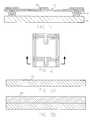
- FIGS. 1E and 3Eshow the microstructures in their released state. As can be seen in FIG. 1E , posts 2 hold the released microstructure on substrate 10 .
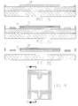
- FIGS. 5 to 7An alternate embodiment to that illustrated in FIG. 1-4 , is illustrated in FIGS. 5 to 7 .
- the mirror formedis not square.
- the micromirrors of the present inventionneed not be square but can have other shapes that may decrease diffraction and increase the contrast ratio, depending upon the position of the light source.
- Such mirrorsare disclosed in U.S. provisional patent application 60/229,246 to Ilkov et al. filed Aug. 30, 2000, and U.S. patent application Ser. No. 09/732,445 to Ilkov et al. filed Dec. 7, 2000, the subject matter of each being incorporated herein by reference.
- the mirror hingescan be flexure hinges as illustrated in the above-mentioned applications and as shown in FIG. 5 of the present application.
- FIGS. 6A to 6 Care cross sections taken along line 6 - 6 of FIG. 5 .
- a substrate 1is provided.
- a sacrificial layer 2is deposited thereon and patterned so as to form holes 6 A, 6 B.
- the sacrificial materialcan be any suitable sacrificial material known in the art, such as amorphous silicon, silicon nitride, silicon oxynitride, silicon dioxide, PSG, amorphous silicon, etc.
- a micromechanical structural layer 7FIG. 6B
- a material different than that of the sacrificial layere.g.
- sacrificial layeris silicon dioxide, silicon nitride if the sacrificial layer is amorphous silicon or polyimide, etc.
- an additional structural layer 8is deposited (after removing part of layer 7 in the hinge areas—not evident in this cross section), followed by depositing a reflective layer 9 (e.g. a metal such as Al, Ag, Au etc.).
- a reflective layer 9e.g. a metal such as Al, Ag, Au etc.
- Layers 2 , 7 , 8 and 9can be deposited by any known methods depending upon the material (spin-on for an organic material such as polyimide, chemical vapor deposition or sputtering for silicon or silicon compounds, sputtering for metal, etc.) and/or as disclosed herein with respect to the other figures.
- layers 7 to 9are patterned by depositing and patterning photoresist followed by etching with a suitable etchant selected for the material(s) being etched (e.g. chlorine chemistry for a metal layer, hydrocarbon or fluorocarbon (or SF6) plasma for silicon or silicon compound layers, etc.). Not shown is the final removal of the sacrificial layer 2 , discussed further herein below.
- a suitable etchantselected for the material(s) being etched (e.g. chlorine chemistry for a metal layer, hydrocarbon or fluorocarbon (or SF6) plasma for silicon or silicon compound layers, etc.
- FIGS. 7A to 7 Cillustrate the same process as in FIGS. 6A to 6 C, but are cross sectional views taken along line 7 - 7 of FIG. 5 .
- the sacrificial layer 2is deposited on substrate 1 , followed by, in FIG. 7B , depositing layer 7 .
- portionsare removed (see gaps in layer 7 in FIG. 7B ). This can be performed with a chlorine , chlorine compound, hydrocarbon, fluorocarbon or other known plasma etch selected based on the composition of layer 7 .
- a chlorine , chlorine compound, hydrocarbon, fluorocarbon or other known plasma etchselected based on the composition of layer 7 .
- layers 8 and 9are deposited over all areas (not shown) followed by patterning to form hinges in the gaps in layer 7 and a corresponding reflective movable mirror element.
- the hingestherefore, are made of layers 8 and 9 (e.g. a silicon or silicon compound layer and a metal layer) and the mirror area is formed of layers 7 to 9 .
- layers 8 and 9e.g. a silicon or silicon compound layer and a metal layer
- the mirror areais formed of layers 7 to 9 .
- the circuitrycan be formed together on the same substrate as the microstructures, such as in U.S. Pat. Nos. 5,061,049, 5,527,744, and 5,872,046. If the microstructures are not formed monolithically on the same wafer as the circuitry, then a second substrate can be provided having circuitry thereon (or, circuitry could be provided on both the first wafer and the replacement substrate if desired). If the microstructures are micromirrors, then it may be preferable to form circuitry and electrodes on a second wafer substrate with at least one electrode electrostatically controlling one pixel (one micromirror on the first wafer portion of the die) of the microdisplay.
- each electrode on the surface of the backplanedetermines whether its corresponding microdisplay pixel is optically ‘on’ or ‘off,’ forming a visible image on the microdisplay.
- the display pixels themselvesare binary, always either fully ‘on’ or fully ‘off,’ and so the backplane design is purely digital. Though the micromirrors could be operated in analog mode, no analog capability is necessary.
- the backplane's I/O and control logicpreferably run at a voltage compatible with standard logic levels, e.g. 5V or 3.3V. To maximize the voltage available to drive the pixels, the backplane's array circuitry may run from a separate supply, preferably at a higher voltage.
- One embodiment of the backplanecan be fabricated in a foundry 5V logic process.
- the mirror electrodescan run at 0-5V or as high above 5V as reliability allows.
- the backplanecould also be fabricated in a higher-voltage process such as a foundry Flash memory process using that process's high-voltage devices.
- the backplanecould also be constructed in a high-voltage process with larger-geometry transistors capable of operating at 12V or more.
- a higher voltage backplanecan produce an electrode voltage swing significantly higher than the 5-7V that the lower voltage backplane provides, and thus actuate the pixels more robustly.
- each electrodeIn digital mode, it is possible to set each electrode to either state (on/off), and have that state persist until the state of the electrode is written again.
- a RAM-like structurewith one bit per pixel is one architecture that accomplishes this.
- One exampleis an SRAM-based pixel cell.
- Alternate well-known storage elementssuch as latches or DRAM (pass transistor plus capacitor) are also possible. If a dynamic storage element (e.g. a DRAM-like cell) is used, it is desirable that it be shielded from incident light that might otherwise cause leakage.
- the perception of a grayscale or full-color imagewill be produced by modulating pixels rapidly on and off, for example according to the method in the above-mentioned U.S. patent application Ser. No. 09/564,069 to Richards.
- the backplaneallows the array to be written in random-access fashion, though finer granularity than a row-at-a-time is generally not necessary.
- the diecan be illuminated with a 200 W or more arc lamp.
- the thermal and photo-carrier effects of thismay result in special layout efforts to make the metal layers as ‘opaque’ as possible over the active circuitry to reflect incident optical energy and minimize photocarrier and thermal effects.
- An on-chip PN diodecould be included for measuring the temperature of the die.
- the resolutionis XGA, 1024 ⁇ 768 pixels, though other resolutions are possible.
- a pixel pitch of from 5 to 24 umis preferred (e.g. 14 um).
- the size of the electrode array itselfis determined by the pixel pitch and resolution.
- a 14 um XGA device's pixel arraywill therefore be 14.336 ⁇ 10.752 mm.
- the I/O pads ( 88 )can be placed along the right edge of the die, as the die is viewed with pixel (0,0) ( 89 in FIG. 5 ) at the top left corner. Putting the pads on the ‘short’ (left/right) edge ( 87 ) of the die is preferable due to the slightly reduced die size.
- the choice of whether the I/O should go on the left vs. right edge of the dieis of little importance since the display controller ASIC may support mirroring the displayed image in the horizontal axis, the vertical axis, or both. If it is desired to orient the display with the I/O on the left edge, the image may simply be rotated 180 degrees by the external display controller.
- the electrode voltage during operationis, in the low state 0V and in the high state preferably from 5 to 7 V (or 12V or higher in the higher voltage design). Of course other voltages are possible, though lower actuation voltages are preferred.
- the electrodesare metal squares, though other geometries are possible. Standard CMOS passivation stackup over the electrodes can be provided.
- the substrate itself, or a deposited sacrificial materialis removed in order to release the micromechanical structures. Removal of substrate of deposited material can also be simply for undercutting (e.g. for a thermal sensor) or for forming wells or trenches (e.g in an integrated circuit process). In any case, the removal/etching of material is preferably performed immediately prior to bonding the just-etched substrate to another substrate (e.g.
- any known substrate or specifically wafer bonding processcould be used, including epoxy bonding (disclosed further below), anodic bonding, fusion bonding, metal thermocompression bonding, etc.).
- the substrate with (preferably released) micromechanical structures, or undercut structuresis bonded to the second substrate with the application of epoxy.
- an optional anti-stiction treatment or other passivation treatment, or treatment for improving epoxy bond strengthcan be applied.
- the treatmentis a self assembled monolayer or lubricant.
- the anti-stiction layeris preferably formed by placing the device in a liquid or gas silane, preferably an alkyl silane, e.g. a chlorosilane known in the art.
- silanes and other materialsare known in the art for their ability to reduce surface contact forces and provide anti-stiction for MEMS structures.
- the release of the micromechanical structures in the present inventionis a multi-step process.
- a first etchis performed that has relatively low selectivity (e.g. less than 200:1, preferably less than 100:1 and more preferably less than 35:1 or even 10:1).
- a second etchfollows has higher selectivity (e.g. greater than 100:1, preferably greater than 200:1 and more preferably greater than 500:1 or even 1000:1).
- the first etchis preferably a gas etch where the etchant is preferably a fluoride etchant, more preferably an energized fluoride gas.
- the energized fluoride gasis energized with, for example, light (e.g.
- UV lightan electric field, or other fields or energy to energize the gas beyond its normal energy as a gas at a particular temperature, such as into a plasma state.
- This energizing of the gas of the inventiongives it a physical component to its etching behavior, in addition to a chemical component.
- Specific examples for energizing the etchant of the first etchinclude using a pair of parallel plate electrodes disposed in a chamber with a gas, and applying electric power of high frequency to the electrodes so that gas discharging takes place to generate gas plasma.
- reactive ion etching and plasma etchingthere are EDR dry etching methods, ion beam etching methods and photo excited etching methods.
- the first etchantcould also be a noble gas which is energized so as to cause a purely physical etch in the first etch (e.g. an Ar or Xe sputter etch).
- These methods for the first etch in the inventionpreferably accomplish the initial etch by causing an interaction physically (Ar sputter) or chemically and physically (plasma fluoride compound) between the energized gas and the material to be removed in making the MEMS device.
- the first etchtherefore, is preferably the result of at least energetic bombardment of the sacrificial material (e.g. by charged species such as positive ions, electrons or negative ions), and possibly additionally a chemical reaction between the etchant gas or gases (e.g. by radicals) and the sacrificial material.
- the first etchutilizes a halogen containing etchant gas that removes the silicon containing sacrificial material both chemically and physically and is preferably a fluorocarbon compound which has carbon and fluorine components (a perfluorocarbon), or carbon, fluorine and hydrogen components (a hydrocarbon).
- a fluorocarbon compoundwhich has carbon and fluorine components (a perfluorocarbon), or carbon, fluorine and hydrogen components (a hydrocarbon).
- Chlorofluorocarbons and bromofluorocarbonse.g. C2F2Cl2, C3F4Cl2, CFCl, C3F2Cl2Br2, CF3Cl, C2F2Br2, CFBr and CF2ClBr
- C2F2Cl2, C3F4Cl2, CFCl, C3F2Cl2Br2, CF3Cl, C2F2Br2, CFBr and CF2ClBrare also possibilities, though they are banned
- the etchant gasis of the formula CxFy, it can be C5F12, C3F6, C2F6, C3F8, C4F8, CF4, C2F4, CF2, C2F6, C4F10, C6F14 or other etchant consisting of carbon and fluorine as is known in the art.
- the etchant gasis a hydrocarbon of the formula CxFyHz, it can be C3HF6, C3H2F6, C3H3F5, CH2F2, C3HF7 or other etchant consisting of carbon, fluorine and hydrogen as is known in the art.
- the etchant of the first etchcould be an oxygenated perfluorocarbon, such as CF3OCHFCF3 or CF3CF2OCF2CHF2.
- the first etchcan alternatively utilize sulfur hexafluoride, or an energized interhalogen or a noble gas halide that etches the sacrificial material both chemically and physically (e.g. RIE/plasma XeF2, IF 5 , BrCl3, BrF3, IF7, ClF3, ClF5, IC1, IBr, etc.).
- the first etch gasis excited with multiple or single wavelengths in the ultraviolet region, preferably in the UV-C region, such as with synchrotron radiation, or preferably with a xenon flash lamp (200 nm and above), a photoionization lamp such as a Cathodeon photoionization lamp (112 nm to 250 nm), a vacuum ultra violet lamp such as a Cathodeon (Deuterium arc source) vacuum ultra violet lamp (112 nm up to 900 nm), or a McPherson Deuterium VUV (emissions continuous between 165 nm and 370 nm).
- a photoionization lampsuch as a Cathodeon photoionization lamp (112 nm to 250 nm
- a vacuum ultra violet lampsuch as a Cathodeon (Deuterium arc source) vacuum ultra violet lamp (112 nm up to 900 nm
- McPherson Deuterium VUVemissions continuous between 165 nm and 370
- a single wavelength excimer lasercould also be used, that has a wavelength that corresponds to an absorption wavelength of the etchant gas.
- an excimer laser emitting a wavelength of 157 nmcould be used to photoionize the XeF2 gas.
- a fluorine lasere.g. a VUV 157 nm GAM laser, Lambda-Physik Novaline F1030—1000 Hz 157 nm fluorine laser, or a Cymer ELX-6500 1000 Hz 157 nm fluorine laser
- a fluorine lasere.g. a VUV 157 nm GAM laser, Lambda-Physik Novaline F1030—1000 Hz 157 nm fluorine laser, or a Cymer ELX-6500 1000 Hz 157 nm fluorine laser
- a plasma etching systeme.g. from MRC, Drytek or Applied Materials, could be used to energize the first etch gas.
- One or more additional gasescan be mixed with the aforementioned etchants for the first etch, including one or more of O2, an inert gas such as Xe or Ar, N2, F2, H2, CO, NxFy (e.g. NF 3), SixFy (e.g. SiF4) or an additional fluorocarbon (with or without a hydrogen component) as above.
- the exact mixture of gases for the first etchcan be optimized for the sacrificial material as known in the art, though it is not necessary that the selectivity be optimized (rather that the primary fluoride containing gas and any additional gases be capable of etching silicon and/or silicon compounds when energized).
- the first etchnot proceed all the way through the thickness of the sacrificial layer. In most cases, the first etch should proceed through 1 ⁇ 4 or less, or preferably ⁇ fraction (1/10) ⁇ or less of the total thickness of the sacrificial layer. Also, it is preferred that the etch proceed for less than 20 minutes, and more preferably less than 10 minutes. The preferred etching depth is 500 angstroms or less and preferably less than 250 angstroms. Such limits on the first etch should result in substantially no undercutting (of etch material from under the micromechanical structural material).
- the second etchutilizes an etchant gas capable of spontaneous chemical etching of the sacrificial material, preferably isotropic etching that chemically (and not physically) removes the sacrificial material.
- an etchant gascapable of spontaneous chemical etching of the sacrificial material, preferably isotropic etching that chemically (and not physically) removes the sacrificial material.
- Such chemical etching and apparatus for performing such chemical etchingare disclosed in U.S. patent application Ser. No. 09/427,841 to Pate et al. filed Oct. 26, 1999, and in U.S. patent application Ser. No. 09/649,569 to Patel at al. filed Aug. 28, 2000, the subject matter of each being incorporated herein by reference.
- Preferred etchants for the second etchare gas phase fluoride etchants that, except for the optional application of temperature, are not energized.
- the second etchmay comprise additional gas components such as N2 or an inert gas (Ar, Xe, He, etc.). Though such gases can be used in the first etch, the difference is that in the first etch they are energized (e.g to a plasma state) to physically and chemically etch the sacrificial material, whereas in the second etch, except for optional heating, the gas is not energized and chemically etches the sacrificial material isotropically. In this way, the remaining sacrificial material is removed and the micromechanical structure is released.
- additional gas componentssuch as N2 or an inert gas (Ar, Xe, He, etc.). Though such gases can be used in the first etch, the difference is that in the first etch they are energized (e.g to a plasma state) to physically and chemically etch the sacrificial material, whereas in the second etch, except for optional heating, the gas is not energized and chemically etches the sacrificial
- BrF3 or XeF2are provided in a plasma-etching chamber with diluent (e.g. N2 and He).
- diluente.g. N2 and He.
- the first etchremoves sacrificial material exposed between micromechanical elements to be released that are from 1 ⁇ 4 to 5 um, preferably from 1 ⁇ 2 to 1 um spaced apart from each other, thus removing “strips” of sacrificial material having an effective width of e.g. from 1 ⁇ 2 to 1 um.
- the depth of sacrificial material removed in the first etchis from 10 to 100 angstroms and is less than ⁇ fraction (1/10) ⁇ th, preferably less than ⁇ fraction (1/20) ⁇ th of the total depth of sacrificial material to be removed by both the first and second etchants.
- each microstructure and substratehas a length and width of from 10 to 1000 um (preferably from 25 to 100 um) and a depth of from 0.25 to 50 um (preferably from 1 to 10 um)—with in most cases the etching undercuts and releases structural layers having a surface area of from 100 to 2500 um 2 .
- a metal layere.g. aluminum in this embodiment is provided prior to performing the first and second etches.
- the first and second etcheswould minimally harm any metal (e.g. Al) provided as part of the microstructures or metallic interconnects, while at the same time being preferably relatively non-selective so as to remove residues such as photoresist, photoresist developer or remover/cleaner, as well as oxides of silicon, silicon, etc.
- An industry standard HF (gas or liquid) washwould not meet these preferred characteristics (higher Al damage, low Si etching, etc.).
- a glass wafersuch as a Coming 1737F, Eagle 2000, quartz or sapphie wafer
- an opaque coatingsuch as a Cr, Ti, Al, TaN, polysilicon or TiN or other opaque coating at a thickness of 2000 angstroms (or more depending upon the material) on the backside of the wafer, in order to make the transparent substrate temporarily opaque for handling.
- an optional adhesion layeris deposited (e.g.
- a plasma enhanced chemical vapor deposition systemsuch as an Applied Materials P5000.
- the sacrificial materialcould be deposited by LPCVD at 560 C, along the lines set forth in U.S. Pat. No. 5,835,256 to Huibers et al., incorporated herein by reference.
- the sacrificial materialcould be deposited by sputtering, or could be a non-silicon containing material such as an organic material (to be later removed by, e.g. plasma oxygen ash).
- the a-Siis patterned (photoresist and etched by a chlorine chemistry, e.g. Cl2, BCl3 and N2), so as to form holes for attachment of the mirror to the glass substrate.
- PECVDRF
- the materialcould be an aluminum alloy (Al—Si (1%), Al—Cu (0.5%) or AlSiCu or AlTi, as well as an implanted or target doped aluminum.
- the backside TiNis etched in a BCl3/Cl2/CF4 chemistry in plasma (or other metal etchant from CRC Handbook of Metal Etchants)—or polished or ground off using CMP, or removed with acid vapor such as HF—followed by a second ACT clean (acetone+DI wafer solution) and a second spin dry.
- the etchis performed by providing the die in a chamber of N2 at around 400 mTorr.
- a second area/chamberhas therein 3.5 mTorr XeF2 and 38.5 mTorr He.
- a barrier between the two areas/chambersis removed, resulting in the combined XeF2, He and N2 etching mixture.
- the transparent wafere.g. Corning 1737F
- TiNtitanium-nitride
- the a-Siis patterned (photoresist and etched by a chlorine chemistry, e.g. C12, BCl3 and N2 ⁇ 50 W), so as to form holes for attachment of the mirror to the glass substrate.
- a second layer of silicon nitrideis deposited by PECVD (same conditions as first layer) at a thickness of 900 Angstroms.
- Alis sputtered (150 C) onto the second silicon nitride layer at a thickness of 500 Angstroms.
- the aluminumis patterned in the P5000 with a chlorine chemistry (BCl3, Cl2, Ar).
- the SiN layersare etched (CHF3, CF4), followed by ashing in a Hitachi barrel asher (O2, CH3OH at 250 C).
- the remaining structuresare cleaned with EKC Technology's EKS265 photoresist residue remover.
- the backside TiNis etched in a SF6/Ar plasma, followed by a second clean and a second spin dry.
- the waferis singulated and each die then is placed in a Drytek parallel plate RF plasma reactor.
- 100 sccm of CF4 and 30 sccm of O2flow to the plasma chamber, which is operated at about 200 mtorr for 80 seconds.
- the dieis etched for 300 seconds at 143 mTorr etch pressure (combined XeF2, He and N2).
- the etchis performed by providing the die in a chamber of N2 at around 400 mTorr.
- a second area/chamberhas therein 5.5 mTorr XeF2 and 20 mTorr He.
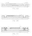
- a substrate 10(silicon or glass) has a sacrificial silicon or silicon compound layer 20 disposed thereon.
- One or more structural layers 30are provided (and patterned) on the sacrificial layer 20 .
- Residue 22 a and 22 b from prior processing steps for forming the micromechanical structures prior to releaseare disposed on sacrificial layer 20 .
- FIG. 9Bafter a first fully physical or physical/chemical etch, a first portion of the sacrificial layer 20 (along with residue 22 a and 22 b ) is removed. Then, as can be seen in FIG.
- FIG. 12 to 14The apparatus for performing the etching of the present invention can be seen in FIG. 12 to 14 .
- an apparatusis provided that includes a source chamber 51 (containing, for example, xenon difluoride crystals for the second etch—the crystals maintained at a temperature of 28.5° C.
- an expansion chamber 52having a volumetric capacity of 29 cubic inches (0.46 liter) to receive xenon difluoride gas from the source chamber 51 , with a shutoff valve 53 joining these two chambers, an etch chamber 54 having a volumetric capacity of 12 cubic inches (0.18 liter) to contain the sample microstructure to be etched, the etch chamber 54 fed by the expansion chamber 52 through a further shutoff valve 55 .
- first gas source 56communicating with the expansion chamber 52 through a further shutoff valve 57
- second gas source 58communicating with the expansion chamber through a separate shutoff valve 59
- a vacuum pump 61 and associated shutoff valves 62 , 63to control the evacuation of the chambers
- a third gas source 64serving as a pump ballast with an associated shutoff valve 65 to prevent backstreaming from the pump 61
- manually operated needle valves 66 , 67 , 68to set the gas flow rates through the various lines and to permit fine adjustments to the pressures in the chambers.
- the expansion chamber 52 and the etch chamber 54were both maintained at a temperature of 35.0° C., while different gases were placed in the first and second gas sources for the various etches.
- the apparatusmay be varied to improve the sample uniformity and reduce the total etch time (by actively moving reaction products away from etch sites and replenishing the etch site with reactant) by placing an agitator in the etch chamber 54 , by including a circulation line between the etch and expansion chambers with a pump in the line to circulate the gas mixture through the etch chamber 54 and the expansion chamber 52 , or by using both of these methods.
- the connecting valve 55 between the expansion chamber 52 and the etch chamber 54was opened, and the shutoff valve 57 at the outlet of the first gas source 56 was opened briefly to allow the gas from the first gas source to enter the expansion and etch chambers to a pressure of about 630 mbar (470 torr).
- the shutoff valve 57was then closed.
- the connecting valve 55was then closed, and the expansion chamber 52 was evacuated and isolated.
- the supply valve 53 from the xenon difluoride source chamber 51was then opened to allow xenon difluoride gas to enter the expansion chamber to a pressure above 8 mbar (6 torr) (due to the higher temperature of the expansion chamber).
- the supply valve 53was then closed, outlet valve 63 was opened, and the needle valve 67 was opened slightly to lower the xenon difluoride pressure in the expansion chamber to 6.7 mbar (5 torr). Both the outlet valve 63 and the needle valve 67 were then closed.
- the shutoff valve 59 at the second gas source 58was then opened and with the assistance of the needle valve 66 , gas from the second gas source was bled into the expansion chamber to a pressure of about 27 mbar (20 torr).
- the expansion chamber 52contained xenon difluoride at 7 mbar (5 torr) plus gas from the second gas source 18 at 20 mbar (15 torr), while the etch chamber 54 contained gas from the first gas source at 630 mbar (470 torr).
- the connecting valve 55 between the expansion chamber 52 and the etch chamber 54was then opened to allow the gas mixture from the expansion chamber to enter the etch chamber as the gases from the two chambers became mixed and distributed between the chambers, thereby beginning the etch process.
- the etch chamberthus contained xenon difluoride at a partial pressure of 4.7 mbar (3.5 torr) gas from the first gas source at a partial pressure of 180 mbar (140 torr) and gas from the second gas source at a partial pressure of 14 mbar (11 torr), thereby resulting in a (second gas):(first gas):(xenon difluoride) volume ratio of 3:39:1.
- the etch processwas continued for as long as needed to remove all of the sacrificial layer, as determined visually, then discontinued.
- FIG. 13represents a different apparatus than that illustrated in FIG. 12 .
- the etchant gas for the second etchoriginates in a source chamber 71 .
- xenon difluorideis used, effective results can be achieved by maintaining the crystals under 40 degrees C. (e.g. at a temperature of 28.5° C.).
- Xenon difluorideis only one of several etchant gases that can be used. Examples of other gases are mentioned elsewhere herein.
- the sublimation pressure of xenon difluoride crystals at 28.5° C.is 5-11 mbar (4-8 torr).
- An expansion chamber 72receives xenon difluoride gas from the crystals in the source chamber(s) 71 , and a shutoff valve 73 is positioned between the source and expansion chambers.
- the sample to be etched 74is placed in an etch chamber 75 , which can contain a baffle 76 and a perforated plate 77 .
- a reciprocating pumpis positioned between the expansion chamber 72 and the etch chamber 75 .
- shutoff valves 91 , 92 , 116 and 119are also shown.
- a third gas source 99serving as a pump ballast with an associated shutoff valve 100 to prevent backstreaming from the pump 123
- manually operated needle valves 101 , 102 , 103 , 104 , 105 , 111 , 115 and 118to set the gas flow rates through the various lines and to permit fine adjustments to the pressures in the chambers.
- the expansion chamber 72 and the etch chamber 75are typically maintained at around room temperature (e.g. 25.0° C.). However, the expansion chamber and etch chamber could also be heated (e.g. to between 25 and 40 degrees C.), though this would likely be performed in conjunction with directly cooling the sample being processed.
- a recirculation line 106permits gas to flow continuously through the etch chamber 75 in a circulation loop that communicates (via valves 96 , 97 , and 104 , 105 ) with the expansion chamber 72 and reenters the etch chamber 75 by way of the reciprocating pump 78 .
- Valve 112permits gas transfer between expansion chamber 72 and etch chamber 75 via a portion of the recirculation line 106 without traversing recirculation pump 78 .
- Valve 113 in path 110permits introduction of etchant gas into the expansion chamber 72 to replenish the etchant mixture during the etching process.
- the valvesare preferably corrosive gas resistant bellows-sealed valves, preferably of aluminum or stainless steel with corrosive resistant O-rings for all seals (e.g. KalrezTM or ChemrazTM).
- the needle valvesare also preferably corrosion resistant, and preferably all stainless steel.
- a filter 109can be placed in the recirculation line 106 to remove etch byproducts from the recirculation flow, thereby reducing the degree of dilution of the etchant gas in the flow.
- the filtercan also serve to reduce the volume of effluents from the process.
- the etch chamber 75can be of any shape or dimensions, but the most favorable results will be achieved when the internal dimensions and shape of the chamber are those that will promote even and steady flow with no vortices or dead volumes in the chamber interior.
- a preferred configuration for the etch chamberis a circular or shallow cylindrical chamber, with a process gas inlet port at the center of the top of the chamber, plus a support in the center of the chamber near the bottom for the sample, and an exit port in the bottom wall or in a side wall below the sample support.
- the baffle 76is placed directly below the entry port.
- the perforated plate 77is wider than the baffle 76 and preferably transmits all gas flow towards the sample.
- the etching chamber of both FIGS. 12 and 13can be provided so as to be capable of energizing one or more gases for the first etch.
- the etching chambercan be provided with a system for creating a plasma in the etching chamber.
- top and bottom electrodesare separated by a grounded diffuser plate 42 that allows gas to be transported between the upper and lower areas.
- the systemcan operate like a conventional RIE, whereas when the upper electrode is powered, the plasma is confined to region 41 between the upper electrode and ground grid 42 .
- remote plasma modethe substrate or wafer 43 is shielded from ion bombardment but free radicals and neutral species can be readily transported to the substrate surface.
- the first etch in the present inventioncan involve one or more of sputter etching, chemical etching, and accelerated ion-assisted etching (each capable of being caused by the plasma system of FIG. 14 , though other ways of causing these types of etching are known).
- accelerated ion-assisted etchinglike the sputtering process, ions are accelerated by the sheath potential. But, unlike sputter etching, the purpose of the accelerated ions are not to sputter away the surface, but rather to damage the surface only, leaving dangling bonds and dislocations in the surface. This is to modify the surface into a more reactive form so that the damaged surface will react with the neutral etchants more easily.
- Sputter etchingis a purely physical process whereby surface materials are being ejected by impinging ions.
- the ionsare propelled by the sheath potentials. Thus, they acquire energy and momentum to knock off the surface materials when they hit on the surface.
- the pressurehas to be low in order for the surface materials to move across the reactor onto opposing surfaces. This is also to prevent ejected materials from colliding with the gas molecules and thus back-scattering onto the surface.
- Chemical etching(during a plasma etch), on the other hand, is a spontaneous reaction between plasma-generated neutral species and substrate material to form volatile gaseous reaction products.
- the apparatus for providing the physical or physical/chemical etchingcan be within the same chamber as for the second etch, as noted above, as part of a second apparatus separate from the apparatus for the second etch, or within a separate chamber but as part of the same apparatus as that used for the second etch. Being provided as part of the same apparatus, whether in the same chamber or not, allows for the first and second etches to take place without exposing the substrate being etched to ambient. In a preferred embodiment, the substrate being etched is not exposed to gases other than gases used in the first or second etch process.
- a load lock(not shown) can also be provided with the appropriate valves for evacuating the load lock chamber.
- one or more sources of additional gasessuch as O2, SF6, a source of the first etchant (e.g. a hydrocarbon or fluorocarbon), N2, Ar, He, or other diluent gas sources or other sources for providing chemical or physical etching, as well as a source of stiction-reducing agent (e.g. an alkyl chlorosilane) could be connected to the etching chamber(s).
- a source of the first etchante.g. a hydrocarbon or fluorocarbon
- N2 ArAr
- Hediluent gas sources or other sources for providing chemical or physical etching
- a source of stiction-reducing agente.g. an alkyl chlorosilane
- the first wafer with such structures thereoncan be packaged (e.g. if circuitry is provided on the first wafer), or the first wafer can be bonded to another wafer having circuitry thereon, in a “flip-chip” type of assembly.
- the bonding of the circuitry wafer to the first wafer holding the microstructurescan be by anodic bonding, metal eutectic bonding, fusion bonding, epoxy bonding, or other wafer bonding processes known in the art.
- a preferred bonding methodis bonding with an IR or UV epoxy such as disclosed in U.S. Pat. No.
- spacerscan be mixed into the epoxy.
- the spacerscan be in the form of spheres or rods and can be dispensed and dispersed between the first wafer and sealing wafer in order to keep the sealing wafer spaced away from the first wafer (so as to avoid damage to the microstructures on the first wafer).
- Spacerscan be dispensed in the gasket area of the display and therefore mixed into the gasket seal material prior to seal dispensing. This is achieved through normal agitated mixing processes.
- the final target for the gap between the first wafer and sealing wafercan be from 1 to 100 um. This of course depends upon the type of MEMS structure being encapsulated and whether it was surface or bulk micromachined (bulk micromachined structures may not need any spacers between the two wafers).
- the spheres or rodscan be made of glass or plastic, preferably an elastically deforming material.
- spacer pillarscan be microfabricated on at least one of the wafer substrates. In one embodiment, pillars/spacers are provided only at the edge of the array. In another embodiment, pillars/spacers can be fabricated in the array itself.
- the spacersare micro-fabricated spacers, they can be formed on the lower wafer, followed by the dispensing of an epoxy, polymer, or other adhesive (e.g. a multi-part epoxy, or a heat or UV-cured adhesive) adjacent to the micro-fabricated spacers.
- the adhesive and spacersneed not be co-located, but could be deposited in different areas on the lower substrate wafer.
- a compression bond materialcould be used that would allow for adhesion of the upper and lower wafers.
- the two wafersare aligned.
- alignment of the opposing electrodes or active viewing areasmay involve registration of substrate fiducials on opposite substrates.
- This taskaccomplished with the aid of video cameras with lens magnification.
- the machinesrange in complexity from manual to fully automated with pattern recognition capability. Whatever the level of sophistication, they accomplish the following process: 1. Dispense a very small amount of a UV curable adhesive at locations near the perimeter and off of all functional devices in the array; 2. Align the fiducials of the opposing substrates within the equipment capability; and 3. Press substrates and UV tack for fixing the wafer to wafer alignment through the remaining bonding process (e.g., curing of the internal epoxy).
- the final cell gapcan be set by pressing the previously tacked laminates in a UV or thermal press.
- a UV pressa common procedure would have the substrates loaded into a press where at least one or both of the press platens are quartz, in order to allow UV radiation from a UV lamp to pass unabated to the gasket seal epoxy.
- Exposure time and flux ratesare process parameters determined by the equipment and adhesive materials.
- Thermally cured epoxiesmay require that the top and bottom platens of a thermal press be heated. The force that can be generated between the press platens is typically many pounds. With thermally cured epoxies, after the initial press the arrays are typically transferred to a stacked press fixture where they can continue to be pressed and post-cured.
- the epoxy between the first wafer and sealing waferis only partially cured so as to allow easier removal of the sealing wafer. After the sealing wafer is removed, this epoxy can be optionally cured.
- An epoxycan be selected that adheres less well (depending upon the wafer materials) than other epoxies, so as to allow for easier removal of the sealing wafer after singulation.
- UV epoxy and IR epoxycan be used at the same time, with the UV epoxy being cured prior to IR cure.
- the assemblycan be separated into individual dies. Scribes are placed on the respective substrates in an offset relationship at least along one direction. The units are then separated, resulting in each unit having a ledge on each end of the die. Such a ledge can also allow for electrical testing of each die, as electrical contacts can be exposed on the ledge (e.g., if circuitry has been formed together with the microstructures on the first wafer). The parts can then be separated from the array by venting the scribes on both substrates. Automatic breaking can be done by commercially available guillotine or fulcrum breaking machines. The parts can also be separated by hand.
- Separationmay also by done by glass scribing and partial sawing of one or both substrates.
- Sawingis preferably done in the presence of a high-pressure jet of water. Moisture must not be allowed to contact the microstructures. Therefore, at gasket dispense, an additional gasket bead must be dispensed around the perimeter of the wafer, or each gasket bead around each die must fully enclose the die area so that water can not enter and touch the microstructures.
- the end of each scribe/saw lanemust be initially left open, to let air vent during the align and press processes. After the array has been pressed and the gasket material fully or partially cured, the vents are then closed using either the gasket or end-seal material. The glass is then scribed and sawed.
- both the first wafer and sealing wafer substratesmay be partially sawed prior to part separation.
- saw lanesare aligned to fiducials on the sealing substrate.
- the glassis sawed to a depth between 25% and 95% of its thickness.
- the first wafer substrateis sawed and the parts separated as described above.
- the first waferupon which the micromechanical structures are formed and released, can be any suitable substrate for the particular MEMS microstructure (and optionally circuitry) formed thereon, such as a light transmissive substrate such as glass, borosilicate, tempered glass, quartz or sapphire, or any other suitable light transmissive material.
- the first wafercould be a metal, ceramic or preferably a semiconductor wafer (e.g. silicon or GaAs).
- An anti-reflective coatingcan be applied to the glass either before processing begins on the glass, or preferably at the time of packaging.
- the second etchinstead of using the previously-mentioned gas phase fluoride non-plasma etchants, could instead use a gas phase acid, such as (non-plasma) HF, HBr, HI, Cl2, combinations thereof (and any such acid(s) with or without H2), non-energized except for being at a high temperature (e.g. 900 C or above).
- a gas phase acidsuch as (non-plasma) HF, HBr, HI, Cl2, combinations thereof (and any such acid(s) with or without H2), non-energized except for being at a high temperature (e.g. 900 C or above).
- the first or second etchcould include BI3, BBr3, BCl3 or AICl3 (plasma etch for the first etch or non-plasma chemical etch for the second).
- the etchcan be performed in pulse or continuous mode.
- the inventionis applicable to forming micromirrors such as for a projection display or optical switch, or any other MEMS device that would benefit from protection of the microstructures during wafer singulation.
- an optical switchis the microstructure being protected, mirrors with multiple hinges can be provided on the first wafer so as to allow for multi-axis movement of the mirror.
- Such multi-axis movement, mirrors for achieving such movement, and methods for making such mirrorsare disclosed in U.S. patent application Ser. No. 09/617,149 to Huibers et al. filed Jul. 17, 2000, the subject matter of which is incorporated herein by reference.
- the microstructureneed not be a movable mirror (for a projection display, for optical switching, or even for data storage), but could be one or more accelerometers, DC relay or RF switches, microlenses, beam splitters, filters, oscillators and antenna system components, variable capacitors and inductors, switched banks of filters, resonant comb-drives and resonant beams, etc.
- Any MEMS structure, particularly a released or movable structure,could benefit from the release method described herein.
Landscapes
- Engineering & Computer Science (AREA)
- Chemical & Material Sciences (AREA)
- Nanotechnology (AREA)
- Microelectronics & Electronic Packaging (AREA)
- Manufacturing & Machinery (AREA)
- Composite Materials (AREA)
- Materials Engineering (AREA)
- Crystallography & Structural Chemistry (AREA)
- General Physics & Mathematics (AREA)
- Condensed Matter Physics & Semiconductors (AREA)
- Physics & Mathematics (AREA)
- Micromachines (AREA)
- Mechanical Light Control Or Optical Switches (AREA)
- Drying Of Semiconductors (AREA)
Abstract
Description
- This application is a divisional of Ser. No. 10/154,150 to Patel, et al filed May 22, 2002, the subject matter being incorporated herein by reference.
- A wide variety of micro-electromechanical devices (MEMS) are known, including accelerometers, DC relay and RF switches, optical cross connects and optical switches, microlenses, reflectors and beam splitters, filters, oscillators and antenna system components, variable capacitors and inductors, switched banks of filters, resonant comb-drives and resonant beams, and micromirror arrays for direct view and projection displays. There are a wide variety of methods for forming MEMS devices, including a) forming micromechanical structures monolithically on the same substrate as actuation or detection circuitry, b) forming the micromechanical structures on a separate substrate and transferring the formed structures to a circuit substrate, c) forming circuitry on one substrate and forming micromechanical elements on another substrate and bonding the substrates side by side or in a flip-chip type arrangement, or d) forming micromechanical structures without any circuitry. Regardless of the actual method used, at some point in the manufacturing process for making MEMS devices, a sacrificial layer is generally removed in order to release the micromechanical structure. The released structure is then able to be actively actuated or moved, such as pivoting or rotation of a micromirror for a projection display or optical switch, or movement during sensing, such as an accelerometer in an automobile airbag system.
- In its most simple form, the invention is directed to etching a material where a first etch removes a portion of the material and fully or partially physically removes the material, and where a subsequent etch removes additional material and removes the material chemically but not physically. The material can be a semiconductor material such as silicon, and the areas removed can be of any dimensions such as an elongated trench, a well or other area limited in size, or even an entire area across a substrate. The result of the first and second etches can also result in an undercut such as for microfluidic channels or for a thermal sensor, or for simply removing material in an IC process.
- In another embodiment, the invention is directed to releasing a micromechanical structure, comprising: providing a substrate; providing a sacrificial layer directly or indirectly on the substrate; providing one or more micromechanical structural layers on the sacrificial layer; performing a first etch to remove a portion of the sacrificial layer, the first etch comprising providing an etchant and energizing the etchant so as to allow the etchant to physically, or chemically and physically, remove the portion of the sacrificial layer; and performing a second etch to remove additional sacrificial material in the sacrificial layer, the second etch comprising providing a second ethant that chemically but not physically etches the additional sacrificial material.
- Another embodiment of the method is for etching a material on or within a substrate, comprising: performing a first etch to remove a portion of the material, the first etch comprising providing an etchant and energizing the etchant so as to allow the etchant to physically, or chemically and physically, remove the portion of the material; and performing a second etch to remove additional silicon, the second etch comprising providing an etchant that chemically but not physically etches the additional material.
- Also disclosed is an apparatus that comprises an etching chamber; connected to the etching chamber, a first source of etchant capable of etching a target material at least partially physically; and connected to the etching chamber, a second source of etchant different from the first source of etchant and capable of etching the target material chemically but not physically.
FIGS. 1A to1E illustrate one method for forming micromirrors;FIG. 2 is a top view of a micromirror showing line1-1 for taking the cross section forFIGS. 1A to1E;FIGS. 3A to3E illustrate the same method as inFIGS. 1A to1D but taken along a different cross section;FIG. 4 is a top view of a mirror showing line3-3 for taking the cross section forFIGS. 3A to3E;FIG. 5 is an illustration of a second embodiment of a micromirror in the present invention;FIGS. 6A to6C are cross sectional views of a method of making the micromirrors ofFIG. 5 , taken along line6-6 inFIG. 5 ;FIGS. 7A to7C are cross sectional views of the method illustrated inFIGS. 6A to6C, taken along line7-7 inFIG. 5 ;FIG. 8 is an illustration of the I/O pads and Si backplane for the embodiment of the invention using separate substrates;FIGS. 9A to9D are cross sectional views illustrating the dual etching steps in the method of the present invention;FIG. 10 is an isometric view of a released microstructure;FIG. 11 is a cross sectional view of a second etch performed without the first etch;FIG. 12 is a view of one embodiment of an apparatus for performing etching in the present invention;FIG. 13 is a view of another embodiment of the apparatus of the present invention; andFIG. 14 is an illustration of further details of the etching chamber for one embodiment of the invention.- Micromechanical Structure Fabrication:
- Processes for microfabricating a MEMS device such as a movable micromirror and mirror array are disclosed in U.S. Pat. Nos. 5,835,256 and 6,046,840 both to Huibers, the subject matter of each being incorporated herein by reference. A similar process for forming MEMS movable elements (e.g. mirrors) on a wafer substrate (e.g. a light transmissive substrate or a substrate comprising CMOS or other circuitry) is illustrated in FIGS.1 to4. By “light transmissive”, it is meant that the material will be transmissive to light at least in operation of the device (The material could temporarily have a light blocking layer on it to improve the ability to handle the substrate during manufacture, or a partial light blocking layer for decreasing light scatter during use. Regardless, a portion of the substrate, for visible light applications, is preferably transmissive to visible light during use so that light can pass into the device, be reflected by the mirrors, and pass back out of the device. Of course, not all embodiments will use a light transmissive substrate). By “wafer” it is meant any substrate on which multiple microstructures or microstructure arrays are to be formed and which allows for being divided into dies, each die having one or more microstructures thereon. Though not in every situation, often each die is one device or product to be packaged and sold separately. Forming multiple “products” or dies on a larger substrate or wafer allows for lower and faster manufacturing costs as compared to forming each die separately. Of course the wafers can be any size or shape, though it is preferred that the wafers be the conventional round or substantially round wafers (e.g. 4″, 6″, 8″ or 12″ in diameter) so as to allow for manufacture in a standard foundry.
FIGS. 1A to1D show a manufacturing process for a micromechanical mirror structure. As can be seen inFIG. 1A , a substrate such as glass (e.g. Corning 1737F), quartz, Pyrex™, sapphire, (or silicon alone or with circuitry thereon) etc. is provided. The cross section of FIGS.1A-D is taken along line1-1 ofFIG. 2 . An optional block layer on the glass surface (not shown) can be provided to block light (incident through the light transmissive substrate during use) from reflecting off of the hinge and potentially causing diffraction and lowering the contrast ratio (if the substrate is transparent).- As can be seen in
FIG. 1B , asacrificial layer 14, such as amorphous silicon, is deposited. The thickness of the sacrificial layer can be wide ranging depending upon the movable element/mirror size and desired tilt angle, though a thickness of from 500 Å to 50,000 Å, preferably around 5000 Å is preferred. Alternatively the sacrificial layer could be polysilicon, silicon nitride, silicon dioxide, polyimide or other organic material, etc. depending upon the materials selected for the structural layers. A lithography step followed by a sacrificial layer etch forms holes16a,bin the sacrificial silicon, which can be any suitable size, though preferably having a diameter of from 0.1 to 1.5 um, more preferably around 0.7±0.25 um. The etching is performed down to the glass/quartz substrate or down to the block layer if present. Preferably if the glass/quartz layer is etched, it is in an amount less than 2000Å. - At this point, as can be seen in
FIG. 1C , afirst layer 18 is deposited by chemical vapor deposition. Preferably the material is silicon nitride or silicon oxide deposited by any suitable method such as sputtering, LPCVD or PECVD, however other materials such as polysilicon, silicon carbide or an organic compound could be deposited at this point (of course the sacrificial layer and at least the etchant of the second etch—to be described below—should be adapted to the material used). The thickness of this first layer can vary depending upon the movable element size and desired amount of stiffness of the element, however in one embodiment the layer has a thickness of from 100 to 3200 Å, more preferably around 1100 Å. The first layer undergoes lithography and etching so as to form holes (0.5 to 1 um in diameter) for posts for holding the MEMS structure on the substrate. - A second layer20 (the “hinge” layer) is deposited as can be seen in
FIG. 1D . By “hinge layer” it is meant the layer that defines that portion of the device that flexes to allow movement of the device. The hinge layer can be disposed only for defining the hinge, or for defining the hinge and other areas such as the mirror. In any case, it is preferred that the first layer is removed in hinge areas prior to depositing the hinge material (second layer). The material for the second (hinge) layer can be the same (e.g. silicon nitride) as the first layer or different (silicon oxide, silicon carbide, polysilicon, etc.) and can be deposited by any suitable method such as sputtering or chemical vapor deposition as for the first layer. The thickness of the second/hinge layer can be greater or less than the first, depending upon the stiffness of the movable element, the flexibility of the hinge desired, the material used, etc. In one embodiment the second layer has a thickness of from 50 Å to 2100 Å, and preferably around 500 Å. In another embodiment, the first layer is deposited by PECVD and the second layer by LPCVD. - As also seen in
FIG. 1D , a reflective andconductive layer 22 is deposited. The reflective/conductive material can be gold, aluminum or other metal, or an alloy of more than one metal though it is preferably aluminum deposited by PVD. The thickness of the metal layer can be from 50 to 2000 Å, preferably around 500 Å. It is also possible to deposit separate reflective and conductive layers. An optional metal passivation layer (not shown) can be added, e.g. a 10 to 1100 Å TiN or TiON layer deposited by PECVD. Then, photoresist patterning on the metal layer is followed by etching through the metal layer with a suitable metal etchant. In the case of an aluminum layer, a chlorine (or bromine) chemistry can be used (e.g. a plasma/RIE etch with Cl2and/or BCl3(or Cl2, CCl4, Br2, CBr4, etc.) with an optional preferably inert diluent such as Ar and/or He). - In the embodiment illustrated in
FIGS. 1A to1D, both the first and second layers are deposited in the area defining the movable element, whereas the second layer, in the absence of the first layer, is deposited in the area of the hinge. It is also possible to use more than two layers to produce a laminate movable element, which can be desirable particularly when the size of the movable element is increased such as for switching light beams in an optical switch. A plurality of layers could be provided in place ofsingle layer 18 inFIG. 1C , and a plurality of layers could be provided in place oflayer 20 and in place oflayer 22. Or, layers20 and22 could be a single layer, e.g. a pure metal layer or a metal alloy layer or a layer that is a mixture of e.g. a dielectric or semiconductor and a metal. Some materials for such layer or layers that could comprise alloys of metals and dielectrics or compounds of metals and nitrogen, oxygen or carbon (particularly the transition metals) are disclosed in U.S. provisional patent application 60/228,007, the subject matter of which is incorporated herein by reference. - Whatever the specific combination, it is desirable that the first/reinforcing layer(s) is provided and patterned (at least in the hinge area) prior to depositing and patterning the hinge material and metal. In one embodiment, the reinforcing layer is removed in the area of the hinge, followed by depositing the hinge layer and patterning both reinforcing and hinge layer together. This joint patterning of the reinforcing layer and hinge layer can be done with the same etchant (e.g. if the two layers are of the same material) or consecutively with different etchants. The reinforcing and hinge layers can be etched with a chlorine chemistry or a fluorine chemistry where the etchant is a perfluorocarbon or hydrofluorocarbon (or SF6) that is energized so as to selectively etch the reinforcing and/or hinge layers both chemically and physically (e.g. a plasma/RIE etch with CF4, CHF3, C3F8, CH2F2, C2F6, SF6, etc. or more likely combinations of the above or with additional gases, such as CF4/H2, SF6/Cl2, or gases using more than one etching species such as CF2Cl2, all possibly with one or more optional inert diluents). Of course, if different materials are used for the reinforcing layer and the hinge layer, then a different etchant can be employed for etching each layer. Alternatively, the reflective layer can be deposited before the first (reinforcing) and/or second (hinge) layer. Whether deposited prior to the hinge material or prior to both the hinge material and the reinforcing material, it is preferable that the metal be patterned (e.g. removed in the hinge area) prior to depositing and patterning the hinge material.
FIGS. 3A to3D illustrate the same process taken along a different cross section (cross section3-3 inFIG. 4 ) and show thesacrificial layer 14 deposited on thelight transmissive substrate 10, followed bylayers metal layer 22. The cross sections inFIGS. 1A to1D and3A to3D are taken along substantially square mirrors inFIGS. 2 and 4 respectively.- It should also be noted that materials and method mentioned above are examples only, as many other method and materials could be used. For example, the Sandia SUMMiT process (using polysilicon for structural layers) or the Cronos MUMPS process (also polysilicon for structural layers) could be used in the present invention. Also, a MOSIS process (AMI ABN-1.5 um CMOS process) could be adapted for the present invention, as could a MUSiC process (using polycrystalline SiC for the structural layers) as disclosed, for example, in Mehregany et al., Thin Solid Films, v. 355-356, pp. 518-524, 1999. Also, though PVD and CVD are referred to above, other thin film deposition methods could be used for depositing the layers, including spin-on, anodization, oxidation, electroplating and evaporation.
- After forming the microstructures as in FIGS.1 to4 on the first wafer, it is preferable to remove the sacrificial layer so as to release the microstructures (in this case micromirrors). The release is described in more detail hereinbelow. This release can be performed at the die level, though it is preferred to perform the release at the wafer level.
FIGS. 1E and 3E show the microstructures in their released state. As can be seen inFIG. 1E , posts2 hold the released microstructure onsubstrate 10. - An alternate embodiment to that illustrated in
FIG. 1-4 , is illustrated in FIGS.5 to7. As can be seen inFIG. 5 , the mirror formed is not square. The micromirrors of the present invention need not be square but can have other shapes that may decrease diffraction and increase the contrast ratio, depending upon the position of the light source. Such mirrors are disclosed in U.S. provisional patent application 60/229,246 to Ilkov et al. filed Aug. 30, 2000, and U.S. patent application Ser. No. 09/732,445 to Ilkov et al. filed Dec. 7, 2000, the subject matter of each being incorporated herein by reference. Also, the mirror hinges can be flexure hinges as illustrated in the above-mentioned applications and as shown inFIG. 5 of the present application. FIGS. 6A to6C are cross sections taken along line6-6 ofFIG. 5 . As can be seen inFIG. 6A , asubstrate 1 is provided. Asacrificial layer 2 is deposited thereon and patterned so as to formholes layer 2 is deposited a micromechanical structural layer7 (FIG. 6B ) of a material different than that of the sacrificial layer (e.g. polysilicon if the sacrificial layer is silicon dioxide, silicon nitride if the sacrificial layer is amorphous silicon or polyimide, etc.). As can be seen inFIG. 6C , an additionalstructural layer 8 is deposited (after removing part oflayer 7 in the hinge areas—not evident in this cross section), followed by depositing a reflective layer9 (e.g. a metal such as Al, Ag, Au etc.).Layers FIG. 6C , layers7 to9 are patterned by depositing and patterning photoresist followed by etching with a suitable etchant selected for the material(s) being etched (e.g. chlorine chemistry for a metal layer, hydrocarbon or fluorocarbon (or SF6) plasma for silicon or silicon compound layers, etc.). Not shown is the final removal of thesacrificial layer 2, discussed further herein below.FIGS. 7A to7C illustrate the same process as inFIGS. 6A to6C, but are cross sectional views taken along line7-7 ofFIG. 5 . As can be seen inFIG. 7A , thesacrificial layer 2 is deposited onsubstrate 1, followed by, inFIG. 7B , depositinglayer 7. After deposition oflayer 7, portions are removed (see gaps inlayer 7 inFIG. 7B ). This can be performed with a chlorine , chlorine compound, hydrocarbon, fluorocarbon or other known plasma etch selected based on the composition oflayer 7. Then, as can be seen inFIG. 7C , layers8 and9 are deposited over all areas (not shown) followed by patterning to form hinges in the gaps inlayer 7 and a corresponding reflective movable mirror element. The hinges, therefore, are made oflayers 8 and9 (e.g. a silicon or silicon compound layer and a metal layer) and the mirror area is formed oflayers 7 to9. Of course there are many variations to the above, such as putting the metal layer down first, forming the hinges or the entire device from a silicon compound-metal alloy (such as in application 60/228,007 mentioned above), or using a single silicon or silicon compound layer and a single metal layer.- Circuitry:
- In the present invention, the circuitry can be formed together on the same substrate as the microstructures, such as in U.S. Pat. Nos. 5,061,049, 5,527,744, and 5,872,046. If the microstructures are not formed monolithically on the same wafer as the circuitry, then a second substrate can be provided having circuitry thereon (or, circuitry could be provided on both the first wafer and the replacement substrate if desired). If the microstructures are micromirrors, then it may be preferable to form circuitry and electrodes on a second wafer substrate with at least one electrode electrostatically controlling one pixel (one micromirror on the first wafer portion of the die) of the microdisplay. The voltage on each electrode on the surface of the backplane determines whether its corresponding microdisplay pixel is optically ‘on’ or ‘off,’ forming a visible image on the microdisplay. Details of the backplane and methods for producing a pulse-width-modulated grayscale or color image are disclosed in U.S. patent application Ser. No. 09/564,069 to Richards, the subject matter of which is incorporated herein by reference.
- The display pixels themselves, in a preferred embodiment, are binary, always either fully ‘on’ or fully ‘off,’ and so the backplane design is purely digital. Though the micromirrors could be operated in analog mode, no analog capability is necessary. For ease of system design, the backplane's I/O and control logic preferably run at a voltage compatible with standard logic levels, e.g. 5V or 3.3V. To maximize the voltage available to drive the pixels, the backplane's array circuitry may run from a separate supply, preferably at a higher voltage.
- One embodiment of the backplane can be fabricated in a foundry 5V logic process. The mirror electrodes can run at 0-5V or as high above 5V as reliability allows. The backplane could also be fabricated in a higher-voltage process such as a foundry Flash memory process using that process's high-voltage devices. The backplane could also be constructed in a high-voltage process with larger-geometry transistors capable of operating at 12V or more. A higher voltage backplane can produce an electrode voltage swing significantly higher than the 5-7V that the lower voltage backplane provides, and thus actuate the pixels more robustly.
- In digital mode, it is possible to set each electrode to either state (on/off), and have that state persist until the state of the electrode is written again. A RAM-like structure, with one bit per pixel is one architecture that accomplishes this. One example is an SRAM-based pixel cell. Alternate well-known storage elements such as latches or DRAM (pass transistor plus capacitor) are also possible. If a dynamic storage element (e.g. a DRAM-like cell) is used, it is desirable that it be shielded from incident light that might otherwise cause leakage.
- The perception of a grayscale or full-color image will be produced by modulating pixels rapidly on and off, for example according to the method in the above-mentioned U.S. patent application Ser. No. 09/564,069 to Richards. In order to support this, it is preferable that the backplane allows the array to be written in random-access fashion, though finer granularity than a row-at-a-time is generally not necessary.
- It is desirable to minimize power consumption, primarily for thermal reasons. Decreasing electrical power dissipation will increase the optical/thermal power budget, allowing the microdisplay to tolerate the heat of more powerful lamps. Also, depending upon the way the microdisplay is assembled (wafer-to-wafer join+offset saw), it may be preferable for all I/O pads to be on one side of the die. To minimize the cost of the finished device it is desirable to minimize pin count. For example, multiplexing row address or other infrequently-used control signals onto the data bus can eliminate separate pins for these functions with a negligible throughput penalty (a few percent, e.g. one clock cycle for address information per row of data is acceptable). A data bus, a clock, and a small number of control signals (5 or less) are preferred.
- In use, the die can be illuminated with a 200 W or more arc lamp. The thermal and photo-carrier effects of this may result in special layout efforts to make the metal layers as ‘opaque’ as possible over the active circuitry to reflect incident optical energy and minimize photocarrier and thermal effects. An on-chip PN diode could be included for measuring the temperature of the die.
- In one embodiment the resolution is XGA, 1024×768 pixels, though other resolutions are possible. A pixel pitch of from 5 to 24 um is preferred (e.g. 14 um). The size of the electrode array itself is determined by the pixel pitch and resolution. A 14 um XGA device's pixel array will therefore be 14.336×10.752 mm.
- As can be seen in
FIG. 8 , the I/O pads (88) can be placed along the right edge of the die, as the die is viewed with pixel (0,0) (89 inFIG. 5 ) at the top left corner. Putting the pads on the ‘short’ (left/right) edge (87) of the die is preferable due to the slightly reduced die size. The choice of whether the I/O should go on the left vs. right edge of the die is of little importance since the display controller ASIC may support mirroring the displayed image in the horizontal axis, the vertical axis, or both. If it is desired to orient the display with the I/O on the left edge, the image may simply be rotated180 degrees by the external display controller. The electrode voltage during operation is, in the low state 0V and in the high state preferably from 5 to 7 V (or 12V or higher in the higher voltage design). Of course other voltages are possible, though lower actuation voltages are preferred. In one embodiment the electrodes are metal squares, though other geometries are possible. Standard CMOS passivation stackup over the electrodes can be provided. - Assembly:
- After depositing and patterning the various micromechanical layers, the substrate itself, or a deposited sacrificial material, is removed in order to release the micromechanical structures. Removal of substrate of deposited material can also be simply for undercutting (e.g. for a thermal sensor) or for forming wells or trenches (e.g in an integrated circuit process). In any case, the removal/etching of material is preferably performed immediately prior to bonding the just-etched substrate to another substrate (e.g. a) a circuit substrate as disclosed hereinabove, b) a permanent silicon, glass or other substrate such as when the micromechanical structures are formed monolithically on the same substrate as actuation, detection or other circuitry, or c) a removable “sacrificial” substrate such as disclosed in U.S. patent application 60/276,222 to Patel et al. filed Mar. 15, 2001. Regardless of the type and purpose of the second substrate to be attached, any known substrate or specifically wafer bonding process could be used, including epoxy bonding (disclosed further below), anodic bonding, fusion bonding, metal thermocompression bonding, etc.). In one embodiment of the invention, the substrate with (preferably released) micromechanical structures, or undercut structures, is bonded to the second substrate with the application of epoxy. Before or after such substrate bonding, an optional anti-stiction treatment or other passivation treatment, or treatment for improving epoxy bond strength, can be applied. If an anti-stiction treatment is performed, in a preferred embodiment the treatment is a self assembled monolayer or lubricant. The anti-stiction layer is preferably formed by placing the device in a liquid or gas silane, preferably an alkyl silane, e.g. a chlorosilane known in the art. Of course, many different silanes and other materials are known in the art for their ability to reduce surface contact forces and provide anti-stiction for MEMS structures.
- The release of the micromechanical structures in the present invention (e.g. micromirrors)—or simple etching—is a multi-step process. A first etch is performed that has relatively low selectivity (e.g. less than 200:1, preferably less than 100:1 and more preferably less than 35:1 or even 10:1). A second etch follows has higher selectivity (e.g. greater than 100:1, preferably greater than 200:1 and more preferably greater than 500:1 or even 1000:1). The first etch is preferably a gas etch where the etchant is preferably a fluoride etchant, more preferably an energized fluoride gas. The energized fluoride gas is energized with, for example, light (e.g. UV light), an electric field, or other fields or energy to energize the gas beyond its normal energy as a gas at a particular temperature, such as into a plasma state. This energizing of the gas of the invention gives it a physical component to its etching behavior, in addition to a chemical component. Specific examples for energizing the etchant of the first etch include using a pair of parallel plate electrodes disposed in a chamber with a gas, and applying electric power of high frequency to the electrodes so that gas discharging takes place to generate gas plasma. Besides reactive ion etching and plasma etching, there are EDR dry etching methods, ion beam etching methods and photo excited etching methods. The first etchant could also be a noble gas which is energized so as to cause a purely physical etch in the first etch (e.g. an Ar or Xe sputter etch). These methods for the first etch in the invention preferably accomplish the initial etch by causing an interaction physically (Ar sputter) or chemically and physically (plasma fluoride compound) between the energized gas and the material to be removed in making the MEMS device. The first etch, therefore, is preferably the result of at least energetic bombardment of the sacrificial material (e.g. by charged species such as positive ions, electrons or negative ions), and possibly additionally a chemical reaction between the etchant gas or gases (e.g. by radicals) and the sacrificial material.
- The first etch utilizes a halogen containing etchant gas that removes the silicon containing sacrificial material both chemically and physically and is preferably a fluorocarbon compound which has carbon and fluorine components (a perfluorocarbon), or carbon, fluorine and hydrogen components (a hydrocarbon). Chlorofluorocarbons and bromofluorocarbons (e.g. C2F2Cl2, C3F4Cl2, CFCl, C3F2Cl2Br2, CF3Cl, C2F2Br2, CFBr and CF2ClBr) are also possibilities, though they are banned in most countries of the world. If the etchant gas is of the formula CxFy, it can be C5F12, C3F6, C2F6, C3F8, C4F8, CF4, C2F4, CF2, C2F6, C4F10, C6F14 or other etchant consisting of carbon and fluorine as is known in the art. If the etchant gas is a hydrocarbon of the formula CxFyHz, it can be C3HF6, C3H2F6, C3H3F5, CH2F2, C3HF7 or other etchant consisting of carbon, fluorine and hydrogen as is known in the art. Or, the etchant of the first etch could be an oxygenated perfluorocarbon, such as CF3OCHFCF3 or CF3CF2OCF2CHF2. The first etch can alternatively utilize sulfur hexafluoride, or an energized interhalogen or a noble gas halide that etches the sacrificial material both chemically and physically (e.g. RIE/plasma XeF2, IF5, BrCl3, BrF3, IF7, ClF3, ClF5, IC1, IBr, etc.).
- In one embodiment, the first etch gas is excited with multiple or single wavelengths in the ultraviolet region, preferably in the UV-C region, such as with synchrotron radiation, or preferably with a xenon flash lamp (200 nm and above), a photoionization lamp such as a Cathodeon photoionization lamp (112 nm to 250 nm), a vacuum ultra violet lamp such as a Cathodeon (Deuterium arc source) vacuum ultra violet lamp (112 nm up to 900 nm), or a McPherson Deuterium VUV (emissions continuous between 165 nm and 370 nm). Of course the spectrum or specific wavelength can be tailored to the etchant gas being used. For example, a single wavelength excimer laser could also be used, that has a wavelength that corresponds to an absorption wavelength of the etchant gas. For example, if the first etch uses XeF2, then an excimer laser emitting a wavelength of 157 nm could be used to photoionize the XeF2 gas. For example, a fluorine laser (e.g. a VUV 157 nm GAM laser, Lambda-Physik Novaline F1030—1000 Hz 157 nm fluorine laser, or a Cymer ELX-6500 1000 Hz 157 nm fluorine laser) that is scanned over the substrate surface or exposes the entire substrate or portions thereof (e.g. die portions) at the same time due to magnification with CaF2 optics (e.g. a catadioptric lens system)—with or without a mask to protect micromechanical structures—can be utilized. In the alternative, a plasma etching system, e.g. from MRC, Drytek or Applied Materials, could be used to energize the first etch gas.
- One or more additional gases can be mixed with the aforementioned etchants for the first etch, including one or more of O2, an inert gas such as Xe or Ar, N2, F2, H2, CO, NxFy (e.g. NF3),SixFy (e.g. SiF4) or an additional fluorocarbon (with or without a hydrogen component) as above. The exact mixture of gases for the first etch can be optimized for the sacrificial material as known in the art, though it is not necessary that the selectivity be optimized (rather that the primary fluoride containing gas and any additional gases be capable of etching silicon and/or silicon compounds when energized). Regardless of which gas or gases are used in the first energized etch, it is preferred that the first etch not proceed all the way through the thickness of the sacrificial layer. In most cases, the first etch should proceed through ¼ or less, or preferably {fraction (1/10)} or less of the total thickness of the sacrificial layer. Also, it is preferred that the etch proceed for less than 20 minutes, and more preferably less than 10 minutes. The preferred etching depth is 500 angstroms or less and preferably less than 250 angstroms. Such limits on the first etch should result in substantially no undercutting (of etch material from under the micromechanical structural material).
- The second etch utilizes an etchant gas capable of spontaneous chemical etching of the sacrificial material, preferably isotropic etching that chemically (and not physically) removes the sacrificial material. Such chemical etching and apparatus for performing such chemical etching are disclosed in U.S. patent application Ser. No. 09/427,841 to Pate et al. filed Oct. 26, 1999, and in U.S. patent application Ser. No. 09/649,569 to Patel at al. filed Aug. 28, 2000, the subject matter of each being incorporated herein by reference. Preferred etchants for the second etch are gas phase fluoride etchants that, except for the optional application of temperature, are not energized. Examples include HF gas, noble gas halides such as xenon difluoride, and interhalogens such as IF5, BrCl3, BrF3, IF7 and ClF3. The second etch may comprise additional gas components such as N2 or an inert gas (Ar, Xe, He, etc.). Though such gases can be used in the first etch, the difference is that in the first etch they are energized (e.g to a plasma state) to physically and chemically etch the sacrificial material, whereas in the second etch, except for optional heating, the gas is not energized and chemically etches the sacrificial material isotropically. In this way, the remaining sacrificial material is removed and the micromechanical structure is released. In one aspect of such an embodiment, BrF3 or XeF2 are provided in a plasma-etching chamber with diluent (e.g. N2 and He). A plasma etch for 1 to 90 minutes, depending upon the concentration of etchant used, is followed by a non-plasma chemical etch using the same interhalogen or noble gas halide.
- In one embodiment, the first etch removes sacrificial material exposed between micromechanical elements to be released that are from ¼ to 5 um, preferably from ½ to 1 um spaced apart from each other, thus removing “strips” of sacrificial material having an effective width of e.g. from ½ to 1 um. The depth of sacrificial material removed in the first etch is from 10 to 100 angstroms and is less than {fraction (1/10)}th, preferably less than {fraction (1/20)}th of the total depth of sacrificial material to be removed by both the first and second etchants. The material removed between each microstructure and substrate has a length and width of from 10 to 1000 um (preferably from 25 to 100 um) and a depth of from 0.25 to 50 um (preferably from 1 to 10 um)—with in most cases the etching undercuts and releases structural layers having a surface area of from 100 to 2500 um2.
- Referring again to
FIGS. 1-4 , it can be seen that a metal layer (e.g. aluminum) in this embodiment is provided prior to performing the first and second etches. As such, in a preferred embodiment of the invention the first and second etches would minimally harm any metal (e.g. Al) provided as part of the microstructures or metallic interconnects, while at the same time being preferably relatively non-selective so as to remove residues such as photoresist, photoresist developer or remover/cleaner, as well as oxides of silicon, silicon, etc. An industry standard HF (gas or liquid) wash would not meet these preferred characteristics (higher Al damage, low Si etching, etc.). - The methods discussed generally above, can be implemented in a number of ways. For example, a glass wafer (such as a Coming 1737F, Eagle 2000, quartz or sapphie wafer) can be provided and coated with an opaque coating, such as a Cr, Ti, Al, TaN, polysilicon or TiN or other opaque coating at a thickness of 2000 angstroms (or more depending upon the material) on the backside of the wafer, in order to make the transparent substrate temporarily opaque for handling. Then, in accordance with
FIGS. 1-4 , after an optional adhesion layer is deposited (e.g. a material with dangling silicon bond such as SiNx—or SiOx, or a conductive material such as vitreous carbon or indium tin oxide) then a sacrificial material of hydrogenated amorphous silicon is deposited (gas=SiH4 (200 sccm), 1500 sccm of Ar, power=100 W, pressure=3.5 T, temp=380 C, electrode spacing=350 mil; or gas=150 sccm of SiHy, 100 sccm of Ar, power=55 W, pressure=3 Torr, temp=380 C, electrode spacing=350 mil; or gas=200 sccm SiH4, 1500 sccm Ar, power=100 W, temp=300 C, pressure=3.5 T; or other process points in between these settings) on the transparent wafer at a thickness of 5000 Angstroms in a plasma enhanced chemical vapor deposition system such as an Applied Materials P5000. Or, the sacrificial material could be deposited by LPCVD at 560 C, along the lines set forth in U.S. Pat. No. 5,835,256 to Huibers et al., incorporated herein by reference. Or, the sacrificial material could be deposited by sputtering, or could be a non-silicon containing material such as an organic material (to be later removed by, e.g. plasma oxygen ash). The a-Si is patterned (photoresist and etched by a chlorine chemistry, e.g. Cl2, BCl3 and N2), so as to form holes for attachment of the mirror to the glass substrate. A first layer of silicon nitride, for creating stiffness in the mirror and for connecting the mirror to the glass, is deposited by PECVD (RF power=150 W, pressure=3 Torr, temp=360 C, electrode spacing=570 mils, gas=N2/SiH4/NH3 (1500/25/10); or RF power=127 W, pressure=2.5 T, temp=380 C, gas=N2/SiH4/NH3 (1500/25/10 sccm), electrode spacing=550 mil, or other process parameters could be used, such as power at 175 W and pressure at 3.5 Torr) at a thickness of 900 Angstroms and is patterned (pressure=800 mT, RF power=100 to 200 W, electrode spacing=0.8 to 1.1 mm, gas=CF4/CHF3/Ar (60 or 70/40 to 70/600 to 800 sccm, He=0 to 200 sccm), so as to remove the silicon nitride in areas in which the mirror hinges will be formed. Next, a second layer of silicon nitride is deposited by PECVD (RF power=127 W, pressure=2.5 T, temp=380 C, gas=N2/SiH4/NH3 (1500/25/10 sccm), electrode spacing=550 mil) at a thickness of 900 Angstroms. Then, Al is sputtered onto the second silicon nitride layer at a thickness of 500 Angstroms at a temp of from 140 to 180 C, power=2000 W, Ar=135 sccm. Or, instead of Al, the material could be an aluminum alloy (Al—Si (1%), Al—Cu (0.5%) or AlSiCu or AlTi, as well as an implanted or target doped aluminum. The aluminum is patterned in the P5000 with a chlorine chemistry (pressure=40 mT, power=550 W, gas=BCl3/Cl2/N2=50/15/30 sccm). Then, the SiN layers are etched (pressure=100 mT, power=460 W, gas=CF4/N2 ({fraction (9/20)} sccm), followed by ashing in a H2O+O2+N2 chemistry in plasma. Next, the remaining structures are ACT cleaned (acetone+DI wafer solution) and spun dry. (this clean can also be done with EKC Technology's EKS265 photoresist residue remover or other solvent based cleaner) After resist coating the frontside of the wafer having the microstructures thereon, the backside TiN is etched in a BCl3/Cl2/CF4 chemistry in plasma (or other metal etchant from CRC Handbook of Metal Etchants)—or polished or ground off using CMP, or removed with acid vapor such as HF—followed by a second ACT clean (acetone+DI wafer solution) and a second spin dry. The wafer is singulated into individual die and each die is exposed to 300 W CF4 plasma (pressure=150 Torr, 85 sccm for 60 seconds, followed by 300 sec etch in a mixture of He, XeF2 and N2 (etch pressure 158 mTorr). The etch is performed by providing the die in a chamber of N2 at around 400 mTorr. A second area/chamber has therein 3.5 mTorr XeF2 and 38.5 mTorr He. A barrier between the two areas/chambers is removed, resulting in the combined XeF2, He and N2 etching mixture. - Or, the transparent wafer (e.g. Corning 1737F) is coated with TiN at a thickness of 2000 angstroms on the backside of the glass wafer. Then, in accordance with
FIGS. 1-4 , without an adhesion layer, a sacrificial material of hydrogenated amorphous silicon is deposited (power=100 W, pressure=3.5 T, temp=300 C, SiH4=200 sccm, Ar=1500 sccm, or pressure=2.5 Torr, power=50 W, temp=360 C, electrode spacing=350 mils, SiH4 flow=200 sccm, Ar flow=2000 sccm) on a glass wafer at a thickness of 5300 Angstroms in an Applied Materials P5000. The a-Si is patterned (photoresist and etched by a chlorine chemistry, e.g. C12, BCl3 and N2 −50 W), so as to form holes for attachment of the mirror to the glass substrate. A first layer of silicon nitride, for creating stifffiess in the mirror and for connecting the mirror to the glass, is deposited by PECVD (pressure=3 Torr, 125 W, 360 C, gap=570, SiH 4=25 sccm, NH3=10 sccm, N2=1500 sccm) at a thickness of 900 Angstroms and is patterned (CF4/CHF3), so as to remove the silicon nitride in areas in which the mirror hinges will be formed. Next, a second layer of silicon nitride is deposited by PECVD (same conditions as first layer) at a thickness of 900 Angstroms. Then, Al is sputtered (150 C) onto the second silicon nitride layer at a thickness of 500 Angstroms. The aluminum is patterned in the P5000 with a chlorine chemistry (BCl3, Cl2, Ar). Then, the SiN layers are etched (CHF3, CF4), followed by ashing in a Hitachi barrel asher (O2, CH3OH at 250 C). Next, the remaining structures are cleaned with EKC Technology's EKS265 photoresist residue remover. After resist coating the frontside of the wafer having the microstructures thereon, the backside TiN is etched in a SF6/Ar plasma, followed by a second clean and a second spin dry. - After depositing the sacrificial and structural layers on a wafer substrate, the wafer is singulated and each die then is placed in a Drytek parallel plate RF plasma reactor. 100 sccm of CF4 and 30 sccm of O2 flow to the plasma chamber, which is operated at about 200 mtorr for 80 seconds. Then, the die is etched for 300 seconds at 143 mTorr etch pressure (combined XeF2, He and N2). The etch is performed by providing the die in a chamber of N2 at around 400 mTorr. A second area/chamber has therein 5.5 mTorr XeF2 and 20 mTorr He. A barrier between the two areas/chambers is removed, resulting in the combined XeF2, He and N2 etching mixture. The above could also be accomplished in a parallel plate plasma etcher with power at 300 W CF4 (150 Torr, 85 sccm) for 120 seconds. Additional features of the second (chemical, non-plasma) etch are disclosed in U.S. patent application Ser. No. 09/427,841 to Patel et al. filed Oct. 26, 1999, and U.S. patent application Ser. No. 09/649,569 to Patel et al. filed Aug. 28, 2000, the subject matter of each being incorporated herein by reference.
- As can further be seen in
FIGS. 9A to D, a substrate10 (silicon or glass) has a sacrificial silicon orsilicon compound layer 20 disposed thereon. One or morestructural layers 30 are provided (and patterned) on thesacrificial layer 20. Residue22aand22bfrom prior processing steps for forming the micromechanical structures prior to release are disposed onsacrificial layer 20. As can be seen inFIG. 9B , after a first fully physical or physical/chemical etch, a first portion of the sacrificial layer20 (along with residue22aand22b) is removed. Then, as can be seen inFIG. 9C , the remainder ofsacrificial layer 20 is in the process of being removed by a purely chemical etch, which ultimately results in releasing themicromechanical structure 30 as can be seen inFIG. 9D andFIG. 10 . As can be seen inFIG. 11 , if the first etch is not performed prior to the second etch, then uneven etching results as illustrated by lines32aand32b. - The apparatus for performing the etching of the present invention can be seen in
FIG. 12 to14. As can be seen inFIG. 12 , an apparatus is provided that includes a source chamber51 (containing, for example, xenon difluoride crystals for the second etch—the crystals maintained at a temperature of 28.5° C. at which temperature the sublimation pressure of the crystals is 5-11 mbar (4-8 torr)), anexpansion chamber 52 having a volumetric capacity of 29 cubic inches (0.46 liter) to receive xenon difluoride gas from thesource chamber 51, with ashutoff valve 53 joining these two chambers, anetch chamber 54 having a volumetric capacity of 12 cubic inches (0.18 liter) to contain the sample microstructure to be etched, theetch chamber 54 fed by theexpansion chamber 52 through afurther shutoff valve 55. Also included in the apparatus is afirst gas source 56 communicating with theexpansion chamber 52 through afurther shutoff valve 57, asecond gas source 58 communicating with the expansion chamber through aseparate shutoff valve 59, avacuum pump 61 and associatedshutoff valves third gas source 64 serving as a pump ballast with an associatedshutoff valve 65 to prevent backstreaming from thepump 61, and manually operatedneedle valves expansion chamber 52 and theetch chamber 54 were both maintained at a temperature of 35.0° C., while different gases were placed in the first and second gas sources for the various etches. - Although not shown in the drawing, the apparatus may be varied to improve the sample uniformity and reduce the total etch time (by actively moving reaction products away from etch sites and replenishing the etch site with reactant) by placing an agitator in the
etch chamber 54, by including a circulation line between the etch and expansion chambers with a pump in the line to circulate the gas mixture through theetch chamber 54 and theexpansion chamber 52, or by using both of these methods. - The general procedure followed in these experiments began with the evacuation of both the
expansion chamber 52 and theetch chamber 54, followed by venting both chambers to atmospheric pressure with gas from thefirst gas source 56 by opening the twoshutoff valves shutoff valves expansion chamber 52 and theetch chamber 54 were evacuated. All valves were then closed. - The connecting
valve 55 between theexpansion chamber 52 and theetch chamber 54 was opened, and theshutoff valve 57 at the outlet of thefirst gas source 56 was opened briefly to allow the gas from the first gas source to enter the expansion and etch chambers to a pressure of about 630 mbar (470 torr). Theshutoff valve 57 was then closed. The connectingvalve 55 was then closed, and theexpansion chamber 52 was evacuated and isolated. Thesupply valve 53 from the xenondifluoride source chamber 51 was then opened to allow xenon difluoride gas to enter the expansion chamber to a pressure above 8 mbar (6 torr) (due to the higher temperature of the expansion chamber). Thesupply valve 53 was then closed,outlet valve 63 was opened, and theneedle valve 67 was opened slightly to lower the xenon difluoride pressure in the expansion chamber to 6.7 mbar (5 torr). Both theoutlet valve 63 and theneedle valve 67 were then closed. Theshutoff valve 59 at thesecond gas source 58 was then opened and with the assistance of theneedle valve 66, gas from the second gas source was bled into the expansion chamber to a pressure of about 27 mbar (20 torr). At this point theexpansion chamber 52 contained xenon difluoride at 7 mbar (5 torr) plus gas from thesecond gas source 18 at 20 mbar (15 torr), while theetch chamber 54 contained gas from the first gas source at 630 mbar (470 torr). - The connecting
valve 55 between theexpansion chamber 52 and theetch chamber 54 was then opened to allow the gas mixture from the expansion chamber to enter the etch chamber as the gases from the two chambers became mixed and distributed between the chambers, thereby beginning the etch process. The etch chamber thus contained xenon difluoride at a partial pressure of 4.7 mbar (3.5 torr) gas from the first gas source at a partial pressure of 180 mbar (140 torr) and gas from the second gas source at a partial pressure of 14 mbar (11 torr), thereby resulting in a (second gas):(first gas):(xenon difluoride) volume ratio of 3:39:1. The etch process was continued for as long as needed to remove all of the sacrificial layer, as determined visually, then discontinued. FIG. 13 represents a different apparatus than that illustrated inFIG. 12 . InFIG. 13 , the etchant gas for the second etch originates in a source chamber71. If xenon difluoride is used, effective results can be achieved by maintaining the crystals under 40 degrees C. (e.g. at a temperature of 28.5° C.). (Xenon difluoride is only one of several etchant gases that can be used. Examples of other gases are mentioned elsewhere herein.) The sublimation pressure of xenon difluoride crystals at 28.5° C. is 5-11 mbar (4-8 torr). Anexpansion chamber 72 receives xenon difluoride gas from the crystals in the source chamber(s)71, and ashutoff valve 73 is positioned between the source and expansion chambers. The sample to be etched74 is placed in anetch chamber 75, which can contain abaffle 76 and aperforated plate 77. A reciprocating pump is positioned between theexpansion chamber 72 and theetch chamber 75.- Also shown are four
individual gas sources expansion chamber 72 throughshutoff valves shutoff valves third gas source 99 serving as a pump ballast with an associatedshutoff valve 100 to prevent backstreaming from the pump123, and manually operatedneedle valves expansion chamber 72 and theetch chamber 75 are typically maintained at around room temperature (e.g. 25.0° C.). However, the expansion chamber and etch chamber could also be heated (e.g. to between 25 and 40 degrees C.), though this would likely be performed in conjunction with directly cooling the sample being processed. Arecirculation line 106 permits gas to flow continuously through theetch chamber 75 in a circulation loop that communicates (viavalves expansion chamber 72 and reenters theetch chamber 75 by way of thereciprocating pump 78.Valve 112 permits gas transfer betweenexpansion chamber 72 andetch chamber 75 via a portion of therecirculation line 106 without traversingrecirculation pump 78.Valve 113 inpath 110 permits introduction of etchant gas into theexpansion chamber 72 to replenish the etchant mixture during the etching process. - The valves are preferably corrosive gas resistant bellows-sealed valves, preferably of aluminum or stainless steel with corrosive resistant O-rings for all seals (e.g. Kalrez™ or Chemraz™). The needle valves are also preferably corrosion resistant, and preferably all stainless steel. As an optional feature, a filter109 can be placed in the
recirculation line 106 to remove etch byproducts from the recirculation flow, thereby reducing the degree of dilution of the etchant gas in the flow. The filter can also serve to reduce the volume of effluents from the process. Theetch chamber 75 can be of any shape or dimensions, but the most favorable results will be achieved when the internal dimensions and shape of the chamber are those that will promote even and steady flow with no vortices or dead volumes in the chamber interior. A preferred configuration for the etch chamber is a circular or shallow cylindrical chamber, with a process gas inlet port at the center of the top of the chamber, plus a support in the center of the chamber near the bottom for the sample, and an exit port in the bottom wall or in a side wall below the sample support. Thebaffle 76 is placed directly below the entry port. Theperforated plate 77 is wider than thebaffle 76 and preferably transmits all gas flow towards the sample. - The etching chamber of both
FIGS. 12 and 13 can be provided so as to be capable of energizing one or more gases for the first etch. For example, the etching chamber can be provided with a system for creating a plasma in the etching chamber. As can be seen inFIG. 14 , top and bottom electrodes are separated by a groundeddiffuser plate 42 that allows gas to be transported between the upper and lower areas. When the lower electrode is powered, the system can operate like a conventional RIE, whereas when the upper electrode is powered, the plasma is confined toregion 41 between the upper electrode andground grid 42. In this mode (“remote plasma mode”) the substrate orwafer 43 is shielded from ion bombardment but free radicals and neutral species can be readily transported to the substrate surface. - The first etch in the present invention can involve one or more of sputter etching, chemical etching, and accelerated ion-assisted etching (each capable of being caused by the plasma system of
FIG. 14 , though other ways of causing these types of etching are known). In accelerated ion-assisted etching, like the sputtering process, ions are accelerated by the sheath potential. But, unlike sputter etching, the purpose of the accelerated ions are not to sputter away the surface, but rather to damage the surface only, leaving dangling bonds and dislocations in the surface. This is to modify the surface into a more reactive form so that the damaged surface will react with the neutral etchants more easily. Sputter etching is a purely physical process whereby surface materials are being ejected by impinging ions. The ions are propelled by the sheath potentials. Thus, they acquire energy and momentum to knock off the surface materials when they hit on the surface. The pressure has to be low in order for the surface materials to move across the reactor onto opposing surfaces. This is also to prevent ejected materials from colliding with the gas molecules and thus back-scattering onto the surface. Chemical etching (during a plasma etch), on the other hand, is a spontaneous reaction between plasma-generated neutral species and substrate material to form volatile gaseous reaction products. - The apparatus for providing the physical or physical/chemical etching can be within the same chamber as for the second etch, as noted above, as part of a second apparatus separate from the apparatus for the second etch, or within a separate chamber but as part of the same apparatus as that used for the second etch. Being provided as part of the same apparatus, whether in the same chamber or not, allows for the first and second etches to take place without exposing the substrate being etched to ambient. In a preferred embodiment, the substrate being etched is not exposed to gases other than gases used in the first or second etch process. A load lock (not shown) can also be provided with the appropriate valves for evacuating the load lock chamber.
- In addition to the etchant for the second etch, illustrated as chamber71 in
FIG. 13 , one or more sources of additional gases, such as O2, SF6, a source of the first etchant (e.g. a hydrocarbon or fluorocarbon), N2, Ar, He, or other diluent gas sources or other sources for providing chemical or physical etching, as well as a source of stiction-reducing agent (e.g. an alkyl chlorosilane) could be connected to the etching chamber(s). These additional gas sources (potentially in liquid or solid form under pressure) are illustrated assources FIG. 13 . Of course additional sources of gases for introduction to the etching apparatus could be provided, and could be provided to separate chambers, depending upon whether a single or multiple chamber apparatus is used. - After releasing the micromechanical structure(s), the first wafer with such structures thereon can be packaged (e.g. if circuitry is provided on the first wafer), or the first wafer can be bonded to another wafer having circuitry thereon, in a “flip-chip” type of assembly. The bonding of the circuitry wafer to the first wafer holding the microstructures can be by anodic bonding, metal eutectic bonding, fusion bonding, epoxy bonding, or other wafer bonding processes known in the art. A preferred bonding method is bonding with an IR or UV epoxy such as disclosed in U.S. Pat. No. 5,963,289 to Stefanov et al, “Asymmetrical Scribe and Separation Method of Manufacturing Liquid Crystal Devices on Silicon Wafers”, which is hereby incorporated by reference. In order to maintain separation between the bonded wafers, spacers can be mixed into the epoxy. The spacers can be in the form of spheres or rods and can be dispensed and dispersed between the first wafer and sealing wafer in order to keep the sealing wafer spaced away from the first wafer (so as to avoid damage to the microstructures on the first wafer). Spacers can be dispensed in the gasket area of the display and therefore mixed into the gasket seal material prior to seal dispensing. This is achieved through normal agitated mixing processes. The final target for the gap between the first wafer and sealing wafer can be from 1 to 100 um. This of course depends upon the type of MEMS structure being encapsulated and whether it was surface or bulk micromachined (bulk micromachined structures may not need any spacers between the two wafers). The spheres or rods can be made of glass or plastic, preferably an elastically deforming material. Alternatively, spacer pillars can be microfabricated on at least one of the wafer substrates. In one embodiment, pillars/spacers are provided only at the edge of the array. In another embodiment, pillars/spacers can be fabricated in the array itself. If the spacers are micro-fabricated spacers, they can be formed on the lower wafer, followed by the dispensing of an epoxy, polymer, or other adhesive (e.g. a multi-part epoxy, or a heat or UV-cured adhesive) adjacent to the micro-fabricated spacers. The adhesive and spacers need not be co-located, but could be deposited in different areas on the lower substrate wafer. Alternative to glue, a compression bond material could be used that would allow for adhesion of the upper and lower wafers. Spacers micro-fabricated on the lower wafer (or the upper wafer) and could be made of polyimide, SU-8 photo-resist.
- Then, the two wafers are aligned. If precision alignment is desired, alignment of the opposing electrodes or active viewing areas may involve registration of substrate fiducials on opposite substrates. This task accomplished with the aid of video cameras with lens magnification. The machines range in complexity from manual to fully automated with pattern recognition capability. Whatever the level of sophistication, they accomplish the following process: 1. Dispense a very small amount of a UV curable adhesive at locations near the perimeter and off of all functional devices in the array; 2. Align the fiducials of the opposing substrates within the equipment capability; and 3. Press substrates and UV tack for fixing the wafer to wafer alignment through the remaining bonding process (e.g., curing of the internal epoxy).
- The final cell gap can be set by pressing the previously tacked laminates in a UV or thermal press. In a UV press, a common procedure would have the substrates loaded into a press where at least one or both of the press platens are quartz, in order to allow UV radiation from a UV lamp to pass unabated to the gasket seal epoxy. Exposure time and flux rates are process parameters determined by the equipment and adhesive materials. Thermally cured epoxies may require that the top and bottom platens of a thermal press be heated. The force that can be generated between the press platens is typically many pounds. With thermally cured epoxies, after the initial press the arrays are typically transferred to a stacked press fixture where they can continue to be pressed and post-cured. In one embodiment, the epoxy between the first wafer and sealing wafer is only partially cured so as to allow easier removal of the sealing wafer. After the sealing wafer is removed, this epoxy can be optionally cured. An epoxy can be selected that adheres less well (depending upon the wafer materials) than other epoxies, so as to allow for easier removal of the sealing wafer after singulation. Also, UV epoxy and IR epoxy can be used at the same time, with the UV epoxy being cured prior to IR cure.
- Once the wafers have been bonded together to form a wafer assembly, the assembly can be separated into individual dies. Scribes are placed on the respective substrates in an offset relationship at least along one direction. The units are then separated, resulting in each unit having a ledge on each end of the die. Such a ledge can also allow for electrical testing of each die, as electrical contacts can be exposed on the ledge (e.g., if circuitry has been formed together with the microstructures on the first wafer). The parts can then be separated from the array by venting the scribes on both substrates. Automatic breaking can be done by commercially available guillotine or fulcrum breaking machines. The parts can also be separated by hand.
- Separation may also by done by glass scribing and partial sawing of one or both substrates. Sawing is preferably done in the presence of a high-pressure jet of water. Moisture must not be allowed to contact the microstructures. Therefore, at gasket dispense, an additional gasket bead must be dispensed around the perimeter of the wafer, or each gasket bead around each die must fully enclose the die area so that water can not enter and touch the microstructures. Preferably, however, the end of each scribe/saw lane must be initially left open, to let air vent during the align and press processes. After the array has been pressed and the gasket material fully or partially cured, the vents are then closed using either the gasket or end-seal material. The glass is then scribed and sawed.
- Alternatively, both the first wafer and sealing wafer substrates may be partially sawed prior to part separation. With the same gasket seal configuration, vent and seal processes as described above, saw lanes are aligned to fiducials on the sealing substrate. The glass is sawed to a depth between 25% and 95% of its thickness. The first wafer substrate is sawed and the parts separated as described above.
- The first wafer, upon which the micromechanical structures are formed and released, can be any suitable substrate for the particular MEMS microstructure (and optionally circuitry) formed thereon, such as a light transmissive substrate such as glass, borosilicate, tempered glass, quartz or sapphire, or any other suitable light transmissive material. Or, the first wafer could be a metal, ceramic or preferably a semiconductor wafer (e.g. silicon or GaAs). An anti-reflective coating can be applied to the glass either before processing begins on the glass, or preferably at the time of packaging.
- There are many variations possible to the preferred embodiments disclosed above. For example, the second etch, instead of using the previously-mentioned gas phase fluoride non-plasma etchants, could instead use a gas phase acid, such as (non-plasma) HF, HBr, HI, Cl2, combinations thereof (and any such acid(s) with or without H2), non-energized except for being at a high temperature (e.g. 900 C or above). Or, either the first or second etch could include BI3, BBr3, BCl3 or AICl3 (plasma etch for the first etch or non-plasma chemical etch for the second). As with any of the etchants, the etch can be performed in pulse or continuous mode.
- It should be noted that the invention is applicable to forming micromirrors such as for a projection display or optical switch, or any other MEMS device that would benefit from protection of the microstructures during wafer singulation. If an optical switch is the microstructure being protected, mirrors with multiple hinges can be provided on the first wafer so as to allow for multi-axis movement of the mirror. Such multi-axis movement, mirrors for achieving such movement, and methods for making such mirrors are disclosed in U.S. patent application Ser. No. 09/617,149 to Huibers et al. filed Jul. 17, 2000, the subject matter of which is incorporated herein by reference.
- Of course, the microstructure need not be a movable mirror (for a projection display, for optical switching, or even for data storage), but could be one or more accelerometers, DC relay or RF switches, microlenses, beam splitters, filters, oscillators and antenna system components, variable capacitors and inductors, switched banks of filters, resonant comb-drives and resonant beams, etc. Any MEMS structure, particularly a released or movable structure, could benefit from the release method described herein.
- The invention has been described in terms of specific embodiments. Nevertheless, persons familiar with the field will appreciate that many variations exist in light of the embodiments described herein.
Claims (43)
Priority Applications (2)
| Application Number | Priority Date | Filing Date | Title |
|---|---|---|---|
| US10/922,565US20050045276A1 (en) | 2001-05-22 | 2004-08-19 | Method for making a micromechanical device by removing a sacrificial layer with multiple sequential etchants |
| US11/303,063US20060096705A1 (en) | 2002-05-22 | 2005-12-14 | Removal of sacrificial materials in MEMS fabrications |
Applications Claiming Priority (3)
| Application Number | Priority Date | Filing Date | Title |
|---|---|---|---|
| US29309201P | 2001-05-22 | 2001-05-22 | |
| US10/154,150US6800210B2 (en) | 2001-05-22 | 2002-05-22 | Method for making a micromechanical device by removing a sacrificial layer with multiple sequential etchants |
| US10/922,565US20050045276A1 (en) | 2001-05-22 | 2004-08-19 | Method for making a micromechanical device by removing a sacrificial layer with multiple sequential etchants |
Related Parent Applications (1)
| Application Number | Title | Priority Date | Filing Date |
|---|---|---|---|
| US10/154,150DivisionUS6800210B2 (en) | 2001-05-22 | 2002-05-22 | Method for making a micromechanical device by removing a sacrificial layer with multiple sequential etchants |
Related Child Applications (1)
| Application Number | Title | Priority Date | Filing Date |
|---|---|---|---|
| US11/303,063Continuation-In-PartUS20060096705A1 (en) | 2002-05-22 | 2005-12-14 | Removal of sacrificial materials in MEMS fabrications |
Publications (1)
| Publication Number | Publication Date |
|---|---|
| US20050045276A1true US20050045276A1 (en) | 2005-03-03 |
Family
ID=23127633
Family Applications (2)
| Application Number | Title | Priority Date | Filing Date |
|---|---|---|---|
| US10/154,150Expired - LifetimeUS6800210B2 (en) | 2001-05-22 | 2002-05-22 | Method for making a micromechanical device by removing a sacrificial layer with multiple sequential etchants |
| US10/922,565AbandonedUS20050045276A1 (en) | 2001-05-22 | 2004-08-19 | Method for making a micromechanical device by removing a sacrificial layer with multiple sequential etchants |
Family Applications Before (1)
| Application Number | Title | Priority Date | Filing Date |
|---|---|---|---|
| US10/154,150Expired - LifetimeUS6800210B2 (en) | 2001-05-22 | 2002-05-22 | Method for making a micromechanical device by removing a sacrificial layer with multiple sequential etchants |
Country Status (3)
| Country | Link |
|---|---|
| US (2) | US6800210B2 (en) |
| AU (1) | AU2002303842A1 (en) |
| WO (1) | WO2002095800A2 (en) |
Cited By (40)
| Publication number | Priority date | Publication date | Assignee | Title |
|---|---|---|---|---|
| US20070105388A1 (en)* | 2005-11-10 | 2007-05-10 | Hynix Semiconductor Inc. | Method for fabricating semiconductor device with recess gate |
| US20070155051A1 (en)* | 2005-12-29 | 2007-07-05 | Chun-Ming Wang | Method of creating MEMS device cavities by a non-etching process |
| US20070284699A1 (en)* | 2006-04-21 | 2007-12-13 | Bioscale, Inc. | Microfabricated Devices and Method for Fabricating Microfabricated Devices |
| US20080029481A1 (en)* | 2006-08-02 | 2008-02-07 | Manish Kothari | Methods for reducing surface charges during the manufacture of microelectromechanical systems devices |
| US20080066860A1 (en)* | 2005-02-24 | 2008-03-20 | International Business Machines Corporation | Ta-TaN SELECTIVE REMOVAL PROCESS FOR INTEGRATED DEVICE FABRICATION |
| EP1902456A1 (en)* | 2005-07-06 | 2008-03-26 | Robert Bosch Gmbh | Reactor for carrying out an etching method for a stack of masked wafers and an etching method |
| US20080094687A1 (en)* | 2006-06-01 | 2008-04-24 | Qualcomm Incorporated | Process and structure for fabrication of mems device having isolated edge posts |
| US20080121611A1 (en)* | 2006-11-27 | 2008-05-29 | Bioscale, Inc. | Micro-fabricated devices having a suspended membrane or plate structure |
| US20080121042A1 (en)* | 2006-11-27 | 2008-05-29 | Bioscale, Inc. | Fluid paths in etchable materials |
| US20080160458A1 (en)* | 2006-12-12 | 2008-07-03 | Asml Netherlands B.V. | Lithographic device manufacturing method, lithographic cell, and computer program product |
| US20080200029A1 (en)* | 2007-02-05 | 2008-08-21 | Sungkyunkwan University | Method of fabricating microstructures |
| US20080213082A1 (en)* | 2007-02-05 | 2008-09-04 | Tokyo Electron Limited | Substrate processing apparatus inspection method and method for reducing quantity of particles on substrate |
| US20080226929A1 (en)* | 2006-01-18 | 2008-09-18 | Qualcomm Mems Technologies, Inc. | Silicon-rich silicon nitrides as etch stop in mems manufacture |
| US20080230519A1 (en)* | 2007-03-23 | 2008-09-25 | Tokyo Electron Limited | Method and system for dry etching a metal nitride |
| US20090022884A1 (en)* | 2004-07-29 | 2009-01-22 | Idc,Llc | System and method for micro-electromechanical operation of an interferometric modulator |
| US20090071932A1 (en)* | 2007-09-14 | 2009-03-19 | Qualcomm Mems Technologies, Inc. | Etching processes used in mems production |
| US20090121158A1 (en)* | 2005-05-27 | 2009-05-14 | Hitachi High-Technologies Corporation | Apparatus and method for specimen fabrication |
| US7534640B2 (en) | 2005-07-22 | 2009-05-19 | Qualcomm Mems Technologies, Inc. | Support structure for MEMS device and methods therefor |
| US7547568B2 (en) | 2006-02-22 | 2009-06-16 | Qualcomm Mems Technologies, Inc. | Electrical conditioning of MEMS device and insulating layer thereof |
| US20090176375A1 (en)* | 2008-01-04 | 2009-07-09 | Benson Russell A | Method of Etching a High Aspect Ratio Contact |
| US7569488B2 (en) | 2007-06-22 | 2009-08-04 | Qualcomm Mems Technologies, Inc. | Methods of making a MEMS device by monitoring a process parameter |
| US7623287B2 (en) | 2006-04-19 | 2009-11-24 | Qualcomm Mems Technologies, Inc. | Non-planar surface structures and process for microelectromechanical systems |
| US20090323168A1 (en)* | 2002-09-20 | 2009-12-31 | Idc, Llc | Electromechanical devices and methods of fabricating same |
| US7719752B2 (en) | 2007-05-11 | 2010-05-18 | Qualcomm Mems Technologies, Inc. | MEMS structures, methods of fabricating MEMS components on separate substrates and assembly of same |
| US7733552B2 (en) | 2007-03-21 | 2010-06-08 | Qualcomm Mems Technologies, Inc | MEMS cavity-coating layers and methods |
| US20100147790A1 (en)* | 2005-07-22 | 2010-06-17 | Qualcomm Mems Technologies, Inc. | Support structure for mems device and methods therefor |
| US20100165442A1 (en)* | 2006-03-02 | 2010-07-01 | Qualcomm Mems Technologies, Inc. | Mems devices with multi-component sacrificial layers |
| US20100183456A1 (en)* | 2006-08-09 | 2010-07-22 | Koninklijke Philips Electronics N.V. | Micro-fluidic system |
| US20100202039A1 (en)* | 2005-08-19 | 2010-08-12 | Qualcomm Mems Technologies, Inc. | Mems devices having support structures with substantially vertical sidewalls and methods for fabricating the same |
| US20100245977A1 (en)* | 2009-03-27 | 2010-09-30 | Qualcomm Mems Technologies, Inc. | Post-release adjustment of interferometric modulator reflectivity |
| US20110256686A1 (en)* | 2007-05-30 | 2011-10-20 | Renesas Electronics Corporation | Semiconductor device and method of manufacturing the same |
| US8278726B2 (en) | 2002-09-20 | 2012-10-02 | Qualcomm Mems Technologies, Inc. | Controlling electromechanical behavior of structures within a microelectromechanical systems device |
| US8358458B2 (en) | 2008-06-05 | 2013-01-22 | Qualcomm Mems Technologies, Inc. | Low temperature amorphous silicon sacrificial layer for controlled adhesion in MEMS devices |
| US20130171573A1 (en)* | 2011-12-30 | 2013-07-04 | Silterra Malaysia Sdn. Bhd. | Method for manufacturing a planarised reflective layer for micromirror devices |
| US20130312835A1 (en)* | 2012-05-25 | 2013-11-28 | Novellus Systems, Inc. | Method and apparatus for rapid pump-down of a high-vacuum loadlock |
| WO2015099761A1 (en) | 2013-12-27 | 2015-07-02 | Intel Corporation | Selective etching for gate all around architectures |
| CN105405806A (en)* | 2014-09-09 | 2016-03-16 | 恩智浦有限公司 | Plasma Etching And Stealth Dicing Laser Process |
| US9728422B2 (en) | 2015-01-23 | 2017-08-08 | Central Glass Company, Limited | Dry etching method |
| TWI621179B (en)* | 2015-01-23 | 2018-04-11 | Central Glass Co Ltd | Dry etching method |
| US20180201496A1 (en)* | 2017-01-16 | 2018-07-19 | Sensortek Technology Corp. | Manufacturing Method of Micro-Electro-Mechanical System Device |
Families Citing this family (116)
| Publication number | Priority date | Publication date | Assignee | Title |
|---|---|---|---|---|
| US6674562B1 (en)* | 1994-05-05 | 2004-01-06 | Iridigm Display Corporation | Interferometric modulation of radiation |
| US7297471B1 (en) | 2003-04-15 | 2007-11-20 | Idc, Llc | Method for manufacturing an array of interferometric modulators |
| US6535318B1 (en)* | 1999-11-12 | 2003-03-18 | Jds Uniphase Corporation | Integrated optoelectronic devices having pop-up mirrors therein and methods of forming and operating same |
| KR100874813B1 (en)* | 2000-11-08 | 2008-12-19 | 다이킨 고교 가부시키가이샤 | Dry etching gas and dry etching method |
| US6992375B2 (en)* | 2000-11-30 | 2006-01-31 | Texas Instruments Incorporated | Anchor for device package |
| EP1220010A3 (en)* | 2000-12-29 | 2004-10-27 | Texas Instruments Incorporated | Micromechanical device recoat methods |
| US7280014B2 (en) | 2001-03-13 | 2007-10-09 | Rochester Institute Of Technology | Micro-electro-mechanical switch and a method of using and making thereof |
| US20030078827A1 (en)* | 2001-03-23 | 2003-04-24 | Hoffman George Harry | System, method and computer program product for strategic supply chain data collection |
| KR100565032B1 (en)* | 2001-03-29 | 2006-03-30 | 가부시키가이샤 도요다 쥬오 겐큐쇼 | Manufacturing apparatus and manufacturing method of silicon structure |
| US6800210B2 (en)* | 2001-05-22 | 2004-10-05 | Reflectivity, Inc. | Method for making a micromechanical device by removing a sacrificial layer with multiple sequential etchants |
| WO2002097865A2 (en)* | 2001-05-31 | 2002-12-05 | Rochester Institute Of Technology | Fluidic valves, agitators, and pumps and methods thereof |
| JP4133810B2 (en)* | 2001-07-10 | 2008-08-13 | 東京エレクトロン株式会社 | Dry etching method |
| EP1282159B1 (en)* | 2001-07-23 | 2004-09-29 | Infineon Technologies AG | Method of forming an isolation layer and method of manufacturing a trench capacitor |
| US7378775B2 (en) | 2001-10-26 | 2008-05-27 | Nth Tech Corporation | Motion based, electrostatic power source and methods thereof |
| US7211923B2 (en) | 2001-10-26 | 2007-05-01 | Nth Tech Corporation | Rotational motion based, electrostatic power source and methods thereof |
| US7106491B2 (en)* | 2001-12-28 | 2006-09-12 | Texas Instruments Incorporated | Split beam micromirror |
| US20070066076A1 (en)* | 2005-09-19 | 2007-03-22 | Bailey Joel B | Substrate processing method and apparatus using a combustion flame |
| WO2003098662A2 (en)* | 2002-05-14 | 2003-11-27 | Tokyo Electron Limited | PLASMA ETCHING OF Cu-CONTAINING LAYERS |
| US20060096705A1 (en)* | 2002-05-22 | 2006-05-11 | Hongqin Shi | Removal of sacrificial materials in MEMS fabrications |
| US6620462B1 (en)* | 2002-05-23 | 2003-09-16 | Taiwan Semiconductor Manufacturing Company | Method to prevent backside TiN cross contamination for reflective product |
| US20040063237A1 (en)* | 2002-09-27 | 2004-04-01 | Chang-Han Yun | Fabricating complex micro-electromechanical systems using a dummy handling substrate |
| US6964882B2 (en)* | 2002-09-27 | 2005-11-15 | Analog Devices, Inc. | Fabricating complex micro-electromechanical systems using a flip bonding technique |
| US6933163B2 (en)* | 2002-09-27 | 2005-08-23 | Analog Devices, Inc. | Fabricating integrated micro-electromechanical systems using an intermediate electrode layer |
| DE10246101B4 (en)* | 2002-10-02 | 2005-12-01 | Infineon Technologies Ag | Method for producing a housing for a chip with a micromechanical structure |
| US6972881B1 (en) | 2002-11-21 | 2005-12-06 | Nuelight Corp. | Micro-electro-mechanical switch (MEMS) display panel with on-glass column multiplexers using MEMS as mux elements |
| TWI220066B (en)* | 2003-03-24 | 2004-08-01 | United Microelectronics Corp | Method of manufacturing a microdisplay |
| US7147713B2 (en)* | 2003-04-30 | 2006-12-12 | Cree, Inc. | Phase controlled sublimation |
| US7247513B2 (en)* | 2003-05-08 | 2007-07-24 | Caracal, Inc. | Dissociation of silicon clusters in a gas phase during chemical vapor deposition homo-epitaxial growth of silicon carbide |
| US7203394B2 (en)* | 2003-07-15 | 2007-04-10 | Rosemount Aerospace Inc. | Micro mirror arrays and microstructures with solderable connection sites |
| JP4427989B2 (en)* | 2003-07-22 | 2010-03-10 | 富士ゼロックス株式会社 | Manufacturing method of microstructure |
| US7287328B2 (en) | 2003-08-29 | 2007-10-30 | Rochester Institute Of Technology | Methods for distributed electrode injection |
| US7217582B2 (en) | 2003-08-29 | 2007-05-15 | Rochester Institute Of Technology | Method for non-damaging charge injection and a system thereof |
| US8529724B2 (en)* | 2003-10-01 | 2013-09-10 | The Charles Stark Draper Laboratory, Inc. | Anodic bonding of silicon carbide to glass |
| US8581308B2 (en) | 2004-02-19 | 2013-11-12 | Rochester Institute Of Technology | High temperature embedded charge devices and methods thereof |
| US7056759B2 (en)* | 2004-04-27 | 2006-06-06 | Hewlett-Packard Development Company, L.P. | Method for making a microelectromechanical system using a flexure protection layer |
| US7541219B2 (en)* | 2004-07-02 | 2009-06-02 | Seagate Technology Llc | Integrated metallic contact probe storage device |
| US20060016783A1 (en)* | 2004-07-22 | 2006-01-26 | Dingjun Wu | Process for titanium nitride removal |
| US7630119B2 (en) | 2004-09-27 | 2009-12-08 | Qualcomm Mems Technologies, Inc. | Apparatus and method for reducing slippage between structures in an interferometric modulator |
| US7527995B2 (en)* | 2004-09-27 | 2009-05-05 | Qualcomm Mems Technologies, Inc. | Method of making prestructure for MEMS systems |
| US7372613B2 (en) | 2004-09-27 | 2008-05-13 | Idc, Llc | Method and device for multistate interferometric light modulation |
| US7289259B2 (en) | 2004-09-27 | 2007-10-30 | Idc, Llc | Conductive bus structure for interferometric modulator array |
| US8008736B2 (en) | 2004-09-27 | 2011-08-30 | Qualcomm Mems Technologies, Inc. | Analog interferometric modulator device |
| US7564612B2 (en) | 2004-09-27 | 2009-07-21 | Idc, Llc | Photonic MEMS and structures |
| US7944599B2 (en) | 2004-09-27 | 2011-05-17 | Qualcomm Mems Technologies, Inc. | Electromechanical device with optical function separated from mechanical and electrical function |
| US7936497B2 (en) | 2004-09-27 | 2011-05-03 | Qualcomm Mems Technologies, Inc. | MEMS device having deformable membrane characterized by mechanical persistence |
| US7583429B2 (en) | 2004-09-27 | 2009-09-01 | Idc, Llc | Ornamental display device |
| US7420725B2 (en) | 2004-09-27 | 2008-09-02 | Idc, Llc | Device having a conductive light absorbing mask and method for fabricating same |
| US20060110688A1 (en)* | 2004-11-19 | 2006-05-25 | Chung-Ju Lee | Etching process compatible with DUV lithography |
| DE102005002967B4 (en)* | 2005-01-21 | 2011-03-31 | Fraunhofer-Gesellschaft zur Förderung der angewandten Forschung e.V. | Method for producing a component with a movable section |
| US7294279B2 (en)* | 2005-03-17 | 2007-11-13 | Taiwan Semiconductor Manufacturing Co., Ltd. | Method for releasing a micromechanical structure |
| US20060245028A1 (en)* | 2005-04-15 | 2006-11-02 | Sriram Ramamoorthi | Light modulator device |
| US7139111B1 (en)* | 2005-04-28 | 2006-11-21 | Taiwan Semiconductor Manufacturing Co., Ltd. | Micromirrors for micro-electro-mechanical systems and methods of fabricating the same |
| US7884989B2 (en) | 2005-05-27 | 2011-02-08 | Qualcomm Mems Technologies, Inc. | White interferometric modulators and methods for forming the same |
| US20070015304A1 (en)* | 2005-07-15 | 2007-01-18 | Jonathan Doan | Low compressive TiNx, materials and methods of making the same |
| US20070123050A1 (en)* | 2005-11-14 | 2007-05-31 | Micron Technology, Inc. | Etch process used during the manufacture of a semiconductor device and systems including the semiconductor device |
| GB0523715D0 (en)* | 2005-11-22 | 2005-12-28 | Cavendish Kinetics Ltd | Method of minimising contact area |
| US7916980B2 (en) | 2006-01-13 | 2011-03-29 | Qualcomm Mems Technologies, Inc. | Interconnect structure for MEMS device |
| US20070197040A1 (en)* | 2006-02-23 | 2007-08-23 | Tokyo Electron Limited | Plasma etching method, plasma etching apparatus, control program and computer-readable storage medium |
| US7883631B2 (en)* | 2006-03-07 | 2011-02-08 | Tokyo Electron Limited | Plasma etching method, plasma etching apparatus, control program and computer-readable storage medium |
| DE102006030323A1 (en)* | 2006-04-21 | 2007-10-25 | Fraunhofer-Gesellschaft zur Förderung der angewandten Forschung e.V. | Process for the surface treatment of a metallic substrate surface |
| US7649671B2 (en) | 2006-06-01 | 2010-01-19 | Qualcomm Mems Technologies, Inc. | Analog interferometric modulator device with electrostatic actuation and release |
| US7527998B2 (en)* | 2006-06-30 | 2009-05-05 | Qualcomm Mems Technologies, Inc. | Method of manufacturing MEMS devices providing air gap control |
| US20080124937A1 (en)* | 2006-08-16 | 2008-05-29 | Songlin Xu | Selective etching method and apparatus |
| US20080072929A1 (en)* | 2006-09-22 | 2008-03-27 | White John M | Dilution gas recirculation |
| US20080072822A1 (en)* | 2006-09-22 | 2008-03-27 | White John M | System and method including a particle trap/filter for recirculating a dilution gas |
| US8115987B2 (en) | 2007-02-01 | 2012-02-14 | Qualcomm Mems Technologies, Inc. | Modulating the intensity of light from an interferometric reflector |
| GB0702837D0 (en)* | 2007-02-14 | 2007-03-28 | Boc Group Plc | Method of treating a gas stream |
| KR20090125087A (en)* | 2007-02-20 | 2009-12-03 | 퀄컴 엠이엠스 테크놀로지스, 인크. | Etching Apparatus and Etching Method of Microelectromechanical System MEMS |
| US7643202B2 (en) | 2007-05-09 | 2010-01-05 | Qualcomm Mems Technologies, Inc. | Microelectromechanical system having a dielectric movable membrane and a mirror |
| JP4925314B2 (en)* | 2007-05-30 | 2012-04-25 | カシオ計算機株式会社 | Silicon nitride film dry etching method and thin film transistor manufacturing method |
| US7630121B2 (en)* | 2007-07-02 | 2009-12-08 | Qualcomm Mems Technologies, Inc. | Electromechanical device with optical function separated from mechanical and electrical function |
| EP2183623A1 (en) | 2007-07-31 | 2010-05-12 | Qualcomm Mems Technologies, Inc. | Devices for enhancing colour shift of interferometric modulators |
| US7847999B2 (en) | 2007-09-14 | 2010-12-07 | Qualcomm Mems Technologies, Inc. | Interferometric modulator display devices |
| US20120057216A1 (en)* | 2007-09-28 | 2012-03-08 | Qualcomm Mems Technologies, Inc. | Multicomponent sacrificial structure |
| CN101828145B (en) | 2007-10-19 | 2012-03-21 | 高通Mems科技公司 | Displays with integrated photovoltaic elements |
| US8058549B2 (en) | 2007-10-19 | 2011-11-15 | Qualcomm Mems Technologies, Inc. | Photovoltaic devices with integrated color interferometric film stacks |
| EP2203765A1 (en) | 2007-10-23 | 2010-07-07 | Qualcomm Mems Technologies, Inc. | Adjustably transmissive mems-based devices |
| US8941631B2 (en) | 2007-11-16 | 2015-01-27 | Qualcomm Mems Technologies, Inc. | Simultaneous light collection and illumination on an active display |
| US8164821B2 (en) | 2008-02-22 | 2012-04-24 | Qualcomm Mems Technologies, Inc. | Microelectromechanical device with thermal expansion balancing layer or stiffening layer |
| US7944604B2 (en) | 2008-03-07 | 2011-05-17 | Qualcomm Mems Technologies, Inc. | Interferometric modulator in transmission mode |
| US7612933B2 (en) | 2008-03-27 | 2009-11-03 | Qualcomm Mems Technologies, Inc. | Microelectromechanical device with spacing layer |
| US7898723B2 (en) | 2008-04-02 | 2011-03-01 | Qualcomm Mems Technologies, Inc. | Microelectromechanical systems display element with photovoltaic structure |
| US7969638B2 (en) | 2008-04-10 | 2011-06-28 | Qualcomm Mems Technologies, Inc. | Device having thin black mask and method of fabricating the same |
| US8163584B2 (en)* | 2008-04-11 | 2012-04-24 | International Business Machines Corporation | Method of minimizing beam bending of MEMS device by reducing the interfacial bonding strength between sacrificial layer and MEMS structure |
| US8023167B2 (en) | 2008-06-25 | 2011-09-20 | Qualcomm Mems Technologies, Inc. | Backlight displays |
| US8358266B2 (en) | 2008-09-02 | 2013-01-22 | Qualcomm Mems Technologies, Inc. | Light turning device with prismatic light turning features |
| DE102008042450A1 (en)* | 2008-09-29 | 2010-04-01 | Robert Bosch Gmbh | Process for structuring silicon carbide using fluorine-containing compounds |
| US9620410B1 (en)* | 2009-01-20 | 2017-04-11 | Lam Research Corporation | Methods for preventing precipitation of etch byproducts during an etch process and/or subsequent rinse process |
| US8270056B2 (en) | 2009-03-23 | 2012-09-18 | Qualcomm Mems Technologies, Inc. | Display device with openings between sub-pixels and method of making same |
| CN102449512A (en) | 2009-05-29 | 2012-05-09 | 高通Mems科技公司 | Illumination devices and methods of fabrication thereof |
| US8270062B2 (en) | 2009-09-17 | 2012-09-18 | Qualcomm Mems Technologies, Inc. | Display device with at least one movable stop element |
| US8488228B2 (en) | 2009-09-28 | 2013-07-16 | Qualcomm Mems Technologies, Inc. | Interferometric display with interferometric reflector |
| KR20130100232A (en) | 2010-04-09 | 2013-09-10 | 퀄컴 엠이엠에스 테크놀로지스, 인크. | Mechanical layer of an electromechanical device and methods of forming the same |
| CN103109315A (en) | 2010-08-17 | 2013-05-15 | 高通Mems科技公司 | Actuation and calibration of a charge neutral electrode in an interferometric display device |
| US9057872B2 (en) | 2010-08-31 | 2015-06-16 | Qualcomm Mems Technologies, Inc. | Dielectric enhanced mirror for IMOD display |
| US8405169B2 (en)* | 2010-10-15 | 2013-03-26 | Taiwan Semiconductor Manufacturing Company, Ltd. | Handling layer for transparent substrate |
| US20120168412A1 (en)* | 2011-01-05 | 2012-07-05 | Electro Scientific Industries, Inc | Apparatus and method for forming an aperture in a substrate |
| US8963159B2 (en) | 2011-04-04 | 2015-02-24 | Qualcomm Mems Technologies, Inc. | Pixel via and methods of forming the same |
| US9134527B2 (en) | 2011-04-04 | 2015-09-15 | Qualcomm Mems Technologies, Inc. | Pixel via and methods of forming the same |
| US8659816B2 (en) | 2011-04-25 | 2014-02-25 | Qualcomm Mems Technologies, Inc. | Mechanical layer and methods of making the same |
| JP6056136B2 (en)* | 2011-09-07 | 2017-01-11 | セントラル硝子株式会社 | Dry etching method |
| JP5932599B2 (en)* | 2011-10-31 | 2016-06-08 | 株式会社日立ハイテクノロジーズ | Plasma etching method |
| TWI497586B (en)* | 2011-10-31 | 2015-08-21 | Hitachi High Tech Corp | Plasma etching method |
| US8736939B2 (en) | 2011-11-04 | 2014-05-27 | Qualcomm Mems Technologies, Inc. | Matching layer thin-films for an electromechanical systems reflective display device |
| US9452926B1 (en)* | 2012-07-30 | 2016-09-27 | The United States Of America As Represented By The Administrator Of National Aeronautics And Space Administration | Dopant selective reactive ion etching of silicon carbide |
| WO2015103003A1 (en)* | 2013-12-30 | 2015-07-09 | E. I. Du Pont De Nemours And Company | Chamber cleaning and semiconductor etching gases |
| US9446947B2 (en)* | 2014-08-25 | 2016-09-20 | Texas Instruments Incorporated | Use of metal native oxide to control stress gradient and bending moment of a released MEMS structure |
| US9975765B1 (en)* | 2015-12-18 | 2018-05-22 | The United States Of America As Represented By The Administrator Of National Aeronautics And Space Administration | Fabricating ultra-thin silicon carbide diaphragms |
| DE102016200506B4 (en) | 2016-01-17 | 2024-05-02 | Robert Bosch Gmbh | Etching device and etching process |
| FR3056824B1 (en)* | 2016-09-26 | 2018-10-26 | Commissariat A L'energie Atomique Et Aux Energies Alternatives | METHOD FOR MANUFACTURING AN INTEGRATED CIRCUIT WITH SEVERAL ACTIVE LAYERS AND INTEGRATED CIRCUIT CORRESPONDING |
| CN108711555B (en)* | 2018-05-22 | 2020-11-13 | 盛吉盛(宁波)半导体科技有限公司 | Silicon wafer etching device for semiconductor integrated circuit |
| US20230006127A1 (en)* | 2019-11-25 | 2023-01-05 | Aita Bio Inc. | Micropump and method of fabricating the same |
| TWI759754B (en)* | 2020-06-03 | 2022-04-01 | 台灣奈米碳素股份有限公司 | Dry etching process for making trench structure of semiconductor device |
| CN114389558B (en)* | 2022-01-13 | 2023-03-10 | 苏州科阳半导体有限公司 | Packaging structure and method of wafer-level FBAR product |
| CN115159440A (en)* | 2022-06-29 | 2022-10-11 | 无锡韦感半导体有限公司 | A kind of sealing structure of micromechanical structure release window and preparation method thereof |
| WO2025019740A1 (en) | 2023-07-20 | 2025-01-23 | The Chemours Company Fc, Llc | Compositions comprising 1,1,1,4,4,4-hexafluoro-2-butyne |
Citations (64)
| Publication number | Priority date | Publication date | Assignee | Title |
|---|---|---|---|---|
| US3511727A (en)* | 1967-05-08 | 1970-05-12 | Motorola Inc | Vapor phase etching and polishing of semiconductors |
| US4190488A (en)* | 1978-08-21 | 1980-02-26 | International Business Machines Corporation | Etching method using noble gas halides |
| US4310380A (en)* | 1980-04-07 | 1982-01-12 | Bell Telephone Laboratories, Incorporated | Plasma etching of silicon |
| US4354897A (en)* | 1980-02-14 | 1982-10-19 | Fujitsu Limited | Process for forming contact through holes |
| US4498953A (en)* | 1983-07-27 | 1985-02-12 | At&T Bell Laboratories | Etching techniques |
| US4528065A (en)* | 1982-11-24 | 1985-07-09 | Semiconductor Energy Laboratory Co., Ltd. | Photoelectric conversion device and its manufacturing method |
| US4529829A (en)* | 1982-11-24 | 1985-07-16 | Semiconductor Energy Laboratory Co., Ltd. | Photoelectric conversion device |
| US4529476A (en)* | 1983-06-01 | 1985-07-16 | Showa Denko K.K. | Gas for selectively etching silicon nitride and process for selectively etching silicon nitride with the gas |
| US4971653A (en)* | 1990-03-14 | 1990-11-20 | Matrix Integrated Systems | Temperature controlled chuck for elevated temperature etch processing |
| US5217501A (en)* | 1989-07-25 | 1993-06-08 | Tokyo Electron Limited | Vertical wafer heat treatment apparatus having dual load lock chambers |
| US5248371A (en)* | 1992-08-13 | 1993-09-28 | General Signal Corporation | Hollow-anode glow discharge apparatus |
| US5298112A (en)* | 1987-08-28 | 1994-03-29 | Kabushiki Kaisha Toshiba | Method for removing composite attached to material by dry etching |
| US5350480A (en)* | 1993-07-23 | 1994-09-27 | Aspect International, Inc. | Surface cleaning and conditioning using hot neutral gas beam array |
| US5409802A (en)* | 1991-03-20 | 1995-04-25 | Canon Kabushiki Kaisha | Method and apparatus for fine processing |
| US5413664A (en)* | 1990-05-09 | 1995-05-09 | Canon Kabushiki Kaisha | Apparatus for preparing a semiconductor device, photo treatment apparatus, pattern forming apparatus and fabrication apparatus |
| US5439553A (en)* | 1994-03-30 | 1995-08-08 | Penn State Research Foundation | Controlled etching of oxides via gas phase reactions |
| US5453305A (en)* | 1991-12-13 | 1995-09-26 | International Business Machines Corporation | Plasma reactor for processing substrates |
| US5534107A (en)* | 1994-06-14 | 1996-07-09 | Fsi International | UV-enhanced dry stripping of silicon nitride films |
| US5629223A (en)* | 1993-12-10 | 1997-05-13 | Micron Technology, Inc. | Method to prepare hemi-spherical grain (HSG) silicon using a fluorine based gas mixture and high vacuum anneal |
| US5683591A (en)* | 1993-05-25 | 1997-11-04 | Robert Bosch Gmbh | Process for producing surface micromechanical structures |
| US5716495A (en)* | 1994-06-14 | 1998-02-10 | Fsi International | Cleaning method |
| US5726480A (en)* | 1995-01-27 | 1998-03-10 | The Regents Of The University Of California | Etchants for use in micromachining of CMOS Microaccelerometers and microelectromechanical devices and method of making the same |
| US5835256A (en)* | 1995-06-19 | 1998-11-10 | Reflectivity, Inc. | Reflective spatial light modulator with encapsulated micro-mechanical elements |
| US5902696A (en)* | 1997-06-02 | 1999-05-11 | Wilson Greatbatch Ltd. | Separator for nonaqueous electrochemical cells |
| US6020272A (en)* | 1998-10-08 | 2000-02-01 | Sandia Corporation | Method for forming suspended micromechanical structures |
| US6046840A (en)* | 1995-06-19 | 2000-04-04 | Reflectivity, Inc. | Double substrate reflective spatial light modulator with self-limiting micro-mechanical elements |
| US6051503A (en)* | 1996-08-01 | 2000-04-18 | Surface Technology Systems Limited | Method of surface treatment of semiconductor substrates |
| US6087615A (en)* | 1996-01-23 | 2000-07-11 | Fraunhofer-Gesellschaft Zur Forderung | Ion source for an ion beam arrangement |
| US6112697A (en)* | 1998-02-19 | 2000-09-05 | Micron Technology, Inc. | RF powered plasma enhanced chemical vapor deposition reactor and methods |
| US6115172A (en)* | 1997-06-30 | 2000-09-05 | Daewoo Electronics Co., Ltd. | Thin film actuated mirror array |
| US6124211A (en)* | 1994-06-14 | 2000-09-26 | Fsi International, Inc. | Cleaning method |
| US6136210A (en)* | 1998-11-02 | 2000-10-24 | Xerox Corporation | Photoetching of acoustic lenses for acoustic ink printing |
| US6143191A (en)* | 1997-11-10 | 2000-11-07 | Advanced Technology Materials, Inc. | Method for etch fabrication of iridium-based electrode structures |
| US6162323A (en)* | 1997-08-12 | 2000-12-19 | Tokyo Electron Yamanashi Limited | Plasma processing apparatus |
| US6162367A (en)* | 1997-01-22 | 2000-12-19 | California Institute Of Technology | Gas-phase silicon etching with bromine trifluoride |
| US6197610B1 (en)* | 2000-01-14 | 2001-03-06 | Ball Semiconductor, Inc. | Method of making small gaps for small electrical/mechanical devices |
| US6204080B1 (en)* | 1997-10-31 | 2001-03-20 | Daewoo Electronics Co., Ltd. | Method for manufacturing thin film actuated mirror array in an optical projection system |
| US6221784B1 (en)* | 1999-11-29 | 2001-04-24 | Applied Materials Inc. | Method and apparatus for sequentially etching a wafer using anisotropic and isotropic etching |
| US6238581B1 (en)* | 1998-12-18 | 2001-05-29 | Eastman Kodak Company | Process for manufacturing an electro-mechanical grating device |
| US6284661B1 (en)* | 1996-04-04 | 2001-09-04 | Daido Hoxan Inc. | Method and apparatus for producing a wafer |
| US6290864B1 (en)* | 1999-10-26 | 2001-09-18 | Reflectivity, Inc. | Fluoride gas etching of silicon with improved selectivity |
| US6290884B1 (en)* | 1998-08-03 | 2001-09-18 | Sumitomo Chemical Company, Limited | Process for producing uncrosslinked polypropylene-based resin foam sheets and uncrosslinked polypropylene-based resin foam sheets |
| US6355181B1 (en)* | 1998-03-20 | 2002-03-12 | Surface Technology Systems Plc | Method and apparatus for manufacturing a micromechanical device |
| US20020033229A1 (en)* | 2000-09-19 | 2002-03-21 | Lebouitz Kyle S. | Apparatus for etching semiconductor samples and a source for providing a gas by sublimination thereto |
| US6372655B2 (en)* | 2000-02-25 | 2002-04-16 | Applied Materials, Inc. | Two etchant etch method |
| US20020047172A1 (en)* | 2000-08-23 | 2002-04-25 | Reid Jason S. | Transition metal dielectric alloy materials for MEMS |
| US6396619B1 (en)* | 2000-01-28 | 2002-05-28 | Reflectivity, Inc. | Deflectable spatial light modulator having stopping mechanisms |
| US6409876B1 (en)* | 1997-05-13 | 2002-06-25 | Surface Technology Systems, Plc | Apparatus for etching a workpiece |
| US20020121502A1 (en)* | 1999-10-26 | 2002-09-05 | Patel Satyadev R. | Method for achieving improved selectivity in an etching process |
| US20020163051A1 (en)* | 2001-05-07 | 2002-11-07 | Applied Materials, Inc. | Microstructure devices, methods of forming a microstructure device and a method of forming a MEMS device |
| US20020164879A1 (en)* | 2001-05-07 | 2002-11-07 | Applied Materials, Inc. | Methods of forming microstructure devices |
| US6483111B1 (en)* | 1998-09-14 | 2002-11-19 | Mitsubishi Denki Kabushiki Kaisha | Thermal infrared-detector array and method of fabrication thereof |
| US20020185699A1 (en)* | 2000-08-23 | 2002-12-12 | Reflectivity, Inc., A Delaware Corporation | MEMS with flexible portions made of novel materials |
| US20020196524A1 (en)* | 2000-08-11 | 2002-12-26 | Reflectivity, Inc. | Deflectable micromirrors with stopping mechanisms |
| US6500356B2 (en)* | 2000-03-27 | 2002-12-31 | Applied Materials, Inc. | Selectively etching silicon using fluorine without plasma |
| US20030054588A1 (en)* | 2000-12-07 | 2003-03-20 | Reflectivity, Inc., A California Corporation | Methods for depositing, releasing and packaging micro-electromechanical devices on wafer substrates |
| US20030071015A1 (en)* | 2001-10-17 | 2003-04-17 | Applied Materials, Inc. | Etch process for etching microstructures |
| US20030077878A1 (en)* | 2001-10-19 | 2003-04-24 | Applied Materials, Inc. | Method for dicing a semiconductor wafer |
| US20030124848A1 (en)* | 2001-10-17 | 2003-07-03 | Applied Materials, Inc. | Method for measuring etch rates during a release process |
| US6646223B2 (en)* | 1999-12-28 | 2003-11-11 | Texas Instruments Incorporated | Method for improving ash rate uniformity in photoresist ashing process equipment |
| US20030219986A1 (en)* | 2002-05-22 | 2003-11-27 | Applied Materials, Inc. | Substrate carrier for processing substrates |
| US6800210B2 (en)* | 2001-05-22 | 2004-10-05 | Reflectivity, Inc. | Method for making a micromechanical device by removing a sacrificial layer with multiple sequential etchants |
| US20050026436A1 (en)* | 2000-12-21 | 2005-02-03 | Hogan Timothy J. | Method for improving ash rate uniformity in photoresist ashing process equipment |
| US6926798B2 (en)* | 1999-11-02 | 2005-08-09 | Tokyo Electron Limited | Apparatus for supercritical processing of a workpiece |
- 2002
- 2002-05-22USUS10/154,150patent/US6800210B2/ennot_activeExpired - Lifetime
- 2002-05-22WOPCT/US2002/016224patent/WO2002095800A2/ennot_activeApplication Discontinuation
- 2002-05-22AUAU2002303842Apatent/AU2002303842A1/ennot_activeAbandoned
- 2004
- 2004-08-19USUS10/922,565patent/US20050045276A1/ennot_activeAbandoned
Patent Citations (70)
| Publication number | Priority date | Publication date | Assignee | Title |
|---|---|---|---|---|
| US3511727A (en)* | 1967-05-08 | 1970-05-12 | Motorola Inc | Vapor phase etching and polishing of semiconductors |
| US4190488A (en)* | 1978-08-21 | 1980-02-26 | International Business Machines Corporation | Etching method using noble gas halides |
| US4354897A (en)* | 1980-02-14 | 1982-10-19 | Fujitsu Limited | Process for forming contact through holes |
| US4310380A (en)* | 1980-04-07 | 1982-01-12 | Bell Telephone Laboratories, Incorporated | Plasma etching of silicon |
| US4710397A (en)* | 1982-11-24 | 1987-12-01 | Semiconductor Energy Laboratory Co., Ltd. | Photoelectric conversion device and its manufacturing method |
| US4528065A (en)* | 1982-11-24 | 1985-07-09 | Semiconductor Energy Laboratory Co., Ltd. | Photoelectric conversion device and its manufacturing method |
| US4529829A (en)* | 1982-11-24 | 1985-07-16 | Semiconductor Energy Laboratory Co., Ltd. | Photoelectric conversion device |
| US4529476A (en)* | 1983-06-01 | 1985-07-16 | Showa Denko K.K. | Gas for selectively etching silicon nitride and process for selectively etching silicon nitride with the gas |
| US4498953A (en)* | 1983-07-27 | 1985-02-12 | At&T Bell Laboratories | Etching techniques |
| US5298112A (en)* | 1987-08-28 | 1994-03-29 | Kabushiki Kaisha Toshiba | Method for removing composite attached to material by dry etching |
| US5217501A (en)* | 1989-07-25 | 1993-06-08 | Tokyo Electron Limited | Vertical wafer heat treatment apparatus having dual load lock chambers |
| US4971653A (en)* | 1990-03-14 | 1990-11-20 | Matrix Integrated Systems | Temperature controlled chuck for elevated temperature etch processing |
| US5413664A (en)* | 1990-05-09 | 1995-05-09 | Canon Kabushiki Kaisha | Apparatus for preparing a semiconductor device, photo treatment apparatus, pattern forming apparatus and fabrication apparatus |
| US5409802A (en)* | 1991-03-20 | 1995-04-25 | Canon Kabushiki Kaisha | Method and apparatus for fine processing |
| US5453305A (en)* | 1991-12-13 | 1995-09-26 | International Business Machines Corporation | Plasma reactor for processing substrates |
| US5248371A (en)* | 1992-08-13 | 1993-09-28 | General Signal Corporation | Hollow-anode glow discharge apparatus |
| US5683591A (en)* | 1993-05-25 | 1997-11-04 | Robert Bosch Gmbh | Process for producing surface micromechanical structures |
| US5350480A (en)* | 1993-07-23 | 1994-09-27 | Aspect International, Inc. | Surface cleaning and conditioning using hot neutral gas beam array |
| US5629223A (en)* | 1993-12-10 | 1997-05-13 | Micron Technology, Inc. | Method to prepare hemi-spherical grain (HSG) silicon using a fluorine based gas mixture and high vacuum anneal |
| US5439553A (en)* | 1994-03-30 | 1995-08-08 | Penn State Research Foundation | Controlled etching of oxides via gas phase reactions |
| US5534107A (en)* | 1994-06-14 | 1996-07-09 | Fsi International | UV-enhanced dry stripping of silicon nitride films |
| US5716495A (en)* | 1994-06-14 | 1998-02-10 | Fsi International | Cleaning method |
| US6124211A (en)* | 1994-06-14 | 2000-09-26 | Fsi International, Inc. | Cleaning method |
| US5726480A (en)* | 1995-01-27 | 1998-03-10 | The Regents Of The University Of California | Etchants for use in micromachining of CMOS Microaccelerometers and microelectromechanical devices and method of making the same |
| US6046840A (en)* | 1995-06-19 | 2000-04-04 | Reflectivity, Inc. | Double substrate reflective spatial light modulator with self-limiting micro-mechanical elements |
| US5835256A (en)* | 1995-06-19 | 1998-11-10 | Reflectivity, Inc. | Reflective spatial light modulator with encapsulated micro-mechanical elements |
| US6087615A (en)* | 1996-01-23 | 2000-07-11 | Fraunhofer-Gesellschaft Zur Forderung | Ion source for an ion beam arrangement |
| US6284661B1 (en)* | 1996-04-04 | 2001-09-04 | Daido Hoxan Inc. | Method and apparatus for producing a wafer |
| US6051503A (en)* | 1996-08-01 | 2000-04-18 | Surface Technology Systems Limited | Method of surface treatment of semiconductor substrates |
| US6436229B2 (en)* | 1997-01-22 | 2002-08-20 | California Institute Of Technology | Gas phase silicon etching with bromine trifluoride |
| US20010002663A1 (en)* | 1997-01-22 | 2001-06-07 | California Institute Of Technology, A Corporation | Gas phase silicon etching with bromine trifluoride |
| US6162367A (en)* | 1997-01-22 | 2000-12-19 | California Institute Of Technology | Gas-phase silicon etching with bromine trifluoride |
| US6409876B1 (en)* | 1997-05-13 | 2002-06-25 | Surface Technology Systems, Plc | Apparatus for etching a workpiece |
| US5902696A (en)* | 1997-06-02 | 1999-05-11 | Wilson Greatbatch Ltd. | Separator for nonaqueous electrochemical cells |
| US6115172A (en)* | 1997-06-30 | 2000-09-05 | Daewoo Electronics Co., Ltd. | Thin film actuated mirror array |
| US6162323A (en)* | 1997-08-12 | 2000-12-19 | Tokyo Electron Yamanashi Limited | Plasma processing apparatus |
| US6204080B1 (en)* | 1997-10-31 | 2001-03-20 | Daewoo Electronics Co., Ltd. | Method for manufacturing thin film actuated mirror array in an optical projection system |
| US6143191A (en)* | 1997-11-10 | 2000-11-07 | Advanced Technology Materials, Inc. | Method for etch fabrication of iridium-based electrode structures |
| US6112697A (en)* | 1998-02-19 | 2000-09-05 | Micron Technology, Inc. | RF powered plasma enhanced chemical vapor deposition reactor and methods |
| US6355181B1 (en)* | 1998-03-20 | 2002-03-12 | Surface Technology Systems Plc | Method and apparatus for manufacturing a micromechanical device |
| US6290884B1 (en)* | 1998-08-03 | 2001-09-18 | Sumitomo Chemical Company, Limited | Process for producing uncrosslinked polypropylene-based resin foam sheets and uncrosslinked polypropylene-based resin foam sheets |
| US6483111B1 (en)* | 1998-09-14 | 2002-11-19 | Mitsubishi Denki Kabushiki Kaisha | Thermal infrared-detector array and method of fabrication thereof |
| US6020272A (en)* | 1998-10-08 | 2000-02-01 | Sandia Corporation | Method for forming suspended micromechanical structures |
| US6136210A (en)* | 1998-11-02 | 2000-10-24 | Xerox Corporation | Photoetching of acoustic lenses for acoustic ink printing |
| US6238581B1 (en)* | 1998-12-18 | 2001-05-29 | Eastman Kodak Company | Process for manufacturing an electro-mechanical grating device |
| US6290864B1 (en)* | 1999-10-26 | 2001-09-18 | Reflectivity, Inc. | Fluoride gas etching of silicon with improved selectivity |
| US20020121502A1 (en)* | 1999-10-26 | 2002-09-05 | Patel Satyadev R. | Method for achieving improved selectivity in an etching process |
| US6926798B2 (en)* | 1999-11-02 | 2005-08-09 | Tokyo Electron Limited | Apparatus for supercritical processing of a workpiece |
| US6221784B1 (en)* | 1999-11-29 | 2001-04-24 | Applied Materials Inc. | Method and apparatus for sequentially etching a wafer using anisotropic and isotropic etching |
| US6646223B2 (en)* | 1999-12-28 | 2003-11-11 | Texas Instruments Incorporated | Method for improving ash rate uniformity in photoresist ashing process equipment |
| US6197610B1 (en)* | 2000-01-14 | 2001-03-06 | Ball Semiconductor, Inc. | Method of making small gaps for small electrical/mechanical devices |
| US6396619B1 (en)* | 2000-01-28 | 2002-05-28 | Reflectivity, Inc. | Deflectable spatial light modulator having stopping mechanisms |
| US6372655B2 (en)* | 2000-02-25 | 2002-04-16 | Applied Materials, Inc. | Two etchant etch method |
| US6500356B2 (en)* | 2000-03-27 | 2002-12-31 | Applied Materials, Inc. | Selectively etching silicon using fluorine without plasma |
| US20020196524A1 (en)* | 2000-08-11 | 2002-12-26 | Reflectivity, Inc. | Deflectable micromirrors with stopping mechanisms |
| US20020185699A1 (en)* | 2000-08-23 | 2002-12-12 | Reflectivity, Inc., A Delaware Corporation | MEMS with flexible portions made of novel materials |
| US20020047172A1 (en)* | 2000-08-23 | 2002-04-25 | Reid Jason S. | Transition metal dielectric alloy materials for MEMS |
| US20020033229A1 (en)* | 2000-09-19 | 2002-03-21 | Lebouitz Kyle S. | Apparatus for etching semiconductor samples and a source for providing a gas by sublimination thereto |
| US20050191790A1 (en)* | 2000-12-07 | 2005-09-01 | Patel Satyadev R. | Methods for depositing, releasing and packaging micro-electromechanical devices on wafer substrates |
| US20030054588A1 (en)* | 2000-12-07 | 2003-03-20 | Reflectivity, Inc., A California Corporation | Methods for depositing, releasing and packaging micro-electromechanical devices on wafer substrates |
| US20050026436A1 (en)* | 2000-12-21 | 2005-02-03 | Hogan Timothy J. | Method for improving ash rate uniformity in photoresist ashing process equipment |
| US20020163051A1 (en)* | 2001-05-07 | 2002-11-07 | Applied Materials, Inc. | Microstructure devices, methods of forming a microstructure device and a method of forming a MEMS device |
| US20030166342A1 (en)* | 2001-05-07 | 2003-09-04 | Applied Materials, Inc. | Integrated method for release and passivation of MEMS structures |
| US6576489B2 (en)* | 2001-05-07 | 2003-06-10 | Applied Materials, Inc. | Methods of forming microstructure devices |
| US20020164879A1 (en)* | 2001-05-07 | 2002-11-07 | Applied Materials, Inc. | Methods of forming microstructure devices |
| US6800210B2 (en)* | 2001-05-22 | 2004-10-05 | Reflectivity, Inc. | Method for making a micromechanical device by removing a sacrificial layer with multiple sequential etchants |
| US20030124848A1 (en)* | 2001-10-17 | 2003-07-03 | Applied Materials, Inc. | Method for measuring etch rates during a release process |
| US20030071015A1 (en)* | 2001-10-17 | 2003-04-17 | Applied Materials, Inc. | Etch process for etching microstructures |
| US20030077878A1 (en)* | 2001-10-19 | 2003-04-24 | Applied Materials, Inc. | Method for dicing a semiconductor wafer |
| US20030219986A1 (en)* | 2002-05-22 | 2003-11-27 | Applied Materials, Inc. | Substrate carrier for processing substrates |
Cited By (83)
| Publication number | Priority date | Publication date | Assignee | Title |
|---|---|---|---|---|
| US20090323168A1 (en)* | 2002-09-20 | 2009-12-31 | Idc, Llc | Electromechanical devices and methods of fabricating same |
| US8278726B2 (en) | 2002-09-20 | 2012-10-02 | Qualcomm Mems Technologies, Inc. | Controlling electromechanical behavior of structures within a microelectromechanical systems device |
| US8368124B2 (en) | 2002-09-20 | 2013-02-05 | Qualcomm Mems Technologies, Inc. | Electromechanical devices having etch barrier layers |
| US8115988B2 (en) | 2004-07-29 | 2012-02-14 | Qualcomm Mems Technologies, Inc. | System and method for micro-electromechanical operation of an interferometric modulator |
| US20090022884A1 (en)* | 2004-07-29 | 2009-01-22 | Idc,Llc | System and method for micro-electromechanical operation of an interferometric modulator |
| US8865597B2 (en) | 2005-02-24 | 2014-10-21 | International Business Machines Corporation | Ta—TaN selective removal process for integrated device fabrication |
| US20080066860A1 (en)* | 2005-02-24 | 2008-03-20 | International Business Machines Corporation | Ta-TaN SELECTIVE REMOVAL PROCESS FOR INTEGRATED DEVICE FABRICATION |
| US20090121158A1 (en)* | 2005-05-27 | 2009-05-14 | Hitachi High-Technologies Corporation | Apparatus and method for specimen fabrication |
| US7989782B2 (en)* | 2005-05-27 | 2011-08-02 | Hitachi High-Technologies Corporation | Apparatus and method for specimen fabrication |
| EP1902456A1 (en)* | 2005-07-06 | 2008-03-26 | Robert Bosch Gmbh | Reactor for carrying out an etching method for a stack of masked wafers and an etching method |
| US20100006427A1 (en)* | 2005-07-06 | 2010-01-14 | Joachim Rudhard | Reactor for carrying out an etching method for a stack of masked wafers and an etching method |
| US20100147790A1 (en)* | 2005-07-22 | 2010-06-17 | Qualcomm Mems Technologies, Inc. | Support structure for mems device and methods therefor |
| US8218229B2 (en) | 2005-07-22 | 2012-07-10 | Qualcomm Mems Technologies, Inc. | Support structure for MEMS device and methods therefor |
| US20100149627A1 (en)* | 2005-07-22 | 2010-06-17 | Qualcomm Mems Technologies, Inc. | Support structure for mems device and methods therefor |
| US7534640B2 (en) | 2005-07-22 | 2009-05-19 | Qualcomm Mems Technologies, Inc. | Support structure for MEMS device and methods therefor |
| US8149497B2 (en) | 2005-07-22 | 2012-04-03 | Qualcomm Mems Technologies, Inc. | Support structure for MEMS device and methods therefor |
| US20100200938A1 (en)* | 2005-08-19 | 2010-08-12 | Qualcomm Mems Technologies, Inc. | Methods for forming layers within a mems device using liftoff processes |
| US20100202039A1 (en)* | 2005-08-19 | 2010-08-12 | Qualcomm Mems Technologies, Inc. | Mems devices having support structures with substantially vertical sidewalls and methods for fabricating the same |
| US8298847B2 (en) | 2005-08-19 | 2012-10-30 | Qualcomm Mems Technologies, Inc. | MEMS devices having support structures with substantially vertical sidewalls and methods for fabricating the same |
| US7835093B2 (en) | 2005-08-19 | 2010-11-16 | Qualcomm Mems Technologies, Inc. | Methods for forming layers within a MEMS device using liftoff processes |
| US7678535B2 (en)* | 2005-11-10 | 2010-03-16 | Hynix Semiconductor, Inc. | Method for fabricating semiconductor device with recess gate |
| US20070105388A1 (en)* | 2005-11-10 | 2007-05-10 | Hynix Semiconductor Inc. | Method for fabricating semiconductor device with recess gate |
| US8394656B2 (en) | 2005-12-29 | 2013-03-12 | Qualcomm Mems Technologies, Inc. | Method of creating MEMS device cavities by a non-etching process |
| US20070155051A1 (en)* | 2005-12-29 | 2007-07-05 | Chun-Ming Wang | Method of creating MEMS device cavities by a non-etching process |
| US7795061B2 (en) | 2005-12-29 | 2010-09-14 | Qualcomm Mems Technologies, Inc. | Method of creating MEMS device cavities by a non-etching process |
| US8064124B2 (en) | 2006-01-18 | 2011-11-22 | Qualcomm Mems Technologies, Inc. | Silicon-rich silicon nitrides as etch stops in MEMS manufacture |
| US20080226929A1 (en)* | 2006-01-18 | 2008-09-18 | Qualcomm Mems Technologies, Inc. | Silicon-rich silicon nitrides as etch stop in mems manufacture |
| US7547568B2 (en) | 2006-02-22 | 2009-06-16 | Qualcomm Mems Technologies, Inc. | Electrical conditioning of MEMS device and insulating layer thereof |
| US20100165442A1 (en)* | 2006-03-02 | 2010-07-01 | Qualcomm Mems Technologies, Inc. | Mems devices with multi-component sacrificial layers |
| US7952789B2 (en) | 2006-03-02 | 2011-05-31 | Qualcomm Mems Technologies, Inc. | MEMS devices with multi-component sacrificial layers |
| US7623287B2 (en) | 2006-04-19 | 2009-11-24 | Qualcomm Mems Technologies, Inc. | Non-planar surface structures and process for microelectromechanical systems |
| US20070284699A1 (en)* | 2006-04-21 | 2007-12-13 | Bioscale, Inc. | Microfabricated Devices and Method for Fabricating Microfabricated Devices |
| US8004021B2 (en) | 2006-04-21 | 2011-08-23 | Bioscale, Inc. | Microfabricated devices and method for fabricating microfabricated devices |
| US7561321B2 (en) | 2006-06-01 | 2009-07-14 | Qualcomm Mems Technologies, Inc. | Process and structure for fabrication of MEMS device having isolated edge posts |
| US20080094687A1 (en)* | 2006-06-01 | 2008-04-24 | Qualcomm Incorporated | Process and structure for fabrication of mems device having isolated edge posts |
| US7763546B2 (en)* | 2006-08-02 | 2010-07-27 | Qualcomm Mems Technologies, Inc. | Methods for reducing surface charges during the manufacture of microelectromechanical systems devices |
| US20080029481A1 (en)* | 2006-08-02 | 2008-02-07 | Manish Kothari | Methods for reducing surface charges during the manufacture of microelectromechanical systems devices |
| US20100183456A1 (en)* | 2006-08-09 | 2010-07-22 | Koninklijke Philips Electronics N.V. | Micro-fluidic system |
| US7999440B2 (en) | 2006-11-27 | 2011-08-16 | Bioscale, Inc. | Micro-fabricated devices having a suspended membrane or plate structure |
| US20080121042A1 (en)* | 2006-11-27 | 2008-05-29 | Bioscale, Inc. | Fluid paths in etchable materials |
| US20080121611A1 (en)* | 2006-11-27 | 2008-05-29 | Bioscale, Inc. | Micro-fabricated devices having a suspended membrane or plate structure |
| US20080160458A1 (en)* | 2006-12-12 | 2008-07-03 | Asml Netherlands B.V. | Lithographic device manufacturing method, lithographic cell, and computer program product |
| US7871471B2 (en)* | 2007-02-05 | 2011-01-18 | Tokyo Electron Limited | Substrate processing apparatus inspection method and method for reducing quantity of particles on substrate |
| US20080200029A1 (en)* | 2007-02-05 | 2008-08-21 | Sungkyunkwan University | Method of fabricating microstructures |
| US20080213082A1 (en)* | 2007-02-05 | 2008-09-04 | Tokyo Electron Limited | Substrate processing apparatus inspection method and method for reducing quantity of particles on substrate |
| US20100245979A1 (en)* | 2007-03-21 | 2010-09-30 | Qualcomm Mems Technologies, Inc. | Mems cavity-coating layers and methods |
| US7733552B2 (en) | 2007-03-21 | 2010-06-08 | Qualcomm Mems Technologies, Inc | MEMS cavity-coating layers and methods |
| US8164815B2 (en) | 2007-03-21 | 2012-04-24 | Qualcomm Mems Technologies, Inc. | MEMS cavity-coating layers and methods |
| US7815814B2 (en)* | 2007-03-23 | 2010-10-19 | Tokyo Electron Limited | Method and system for dry etching a metal nitride |
| US20080230519A1 (en)* | 2007-03-23 | 2008-09-25 | Tokyo Electron Limited | Method and system for dry etching a metal nitride |
| US8284475B2 (en) | 2007-05-11 | 2012-10-09 | Qualcomm Mems Technologies, Inc. | Methods of fabricating MEMS with spacers between plates and devices formed by same |
| US20100182675A1 (en)* | 2007-05-11 | 2010-07-22 | Qualcomm Mems Technologies, Inc. | Methods of fabricating mems with spacers between plates and devices formed by same |
| US7719752B2 (en) | 2007-05-11 | 2010-05-18 | Qualcomm Mems Technologies, Inc. | MEMS structures, methods of fabricating MEMS components on separate substrates and assembly of same |
| US8830557B2 (en) | 2007-05-11 | 2014-09-09 | Qualcomm Mems Technologies, Inc. | Methods of fabricating MEMS with spacers between plates and devices formed by same |
| US8748282B2 (en)* | 2007-05-30 | 2014-06-10 | Renesas Electronics Corporation | Semiconductor device and method of manufacturing the same |
| US20110256686A1 (en)* | 2007-05-30 | 2011-10-20 | Renesas Electronics Corporation | Semiconductor device and method of manufacturing the same |
| US7569488B2 (en) | 2007-06-22 | 2009-08-04 | Qualcomm Mems Technologies, Inc. | Methods of making a MEMS device by monitoring a process parameter |
| US20090101623A1 (en)* | 2007-09-14 | 2009-04-23 | Qualcomm Mems Technologies, Inc. | Etching processes used in mems production |
| US20090071933A1 (en)* | 2007-09-14 | 2009-03-19 | Qualcomm Mems Technologies, Inc. | Etching processes used in mems production |
| US8308962B2 (en) | 2007-09-14 | 2012-11-13 | Qualcomm Mems Technologies, Inc. | Etching processes used in MEMS production |
| US8323516B2 (en)* | 2007-09-14 | 2012-12-04 | Qualcomm Mems Technologies, Inc. | Etching processes used in MEMS production |
| US20090074646A1 (en)* | 2007-09-14 | 2009-03-19 | Qualcomm Mems Technologies, Inc. | Etching processes used in mems production |
| US20090071932A1 (en)* | 2007-09-14 | 2009-03-19 | Qualcomm Mems Technologies, Inc. | Etching processes used in mems production |
| TWI402908B (en)* | 2008-01-04 | 2013-07-21 | Micron Technology Inc | Method of etching a high aspect ratio contact |
| US20090176375A1 (en)* | 2008-01-04 | 2009-07-09 | Benson Russell A | Method of Etching a High Aspect Ratio Contact |
| US8614151B2 (en)* | 2008-01-04 | 2013-12-24 | Micron Technology, Inc. | Method of etching a high aspect ratio contact |
| US8358458B2 (en) | 2008-06-05 | 2013-01-22 | Qualcomm Mems Technologies, Inc. | Low temperature amorphous silicon sacrificial layer for controlled adhesion in MEMS devices |
| US7864403B2 (en) | 2009-03-27 | 2011-01-04 | Qualcomm Mems Technologies, Inc. | Post-release adjustment of interferometric modulator reflectivity |
| US20100245977A1 (en)* | 2009-03-27 | 2010-09-30 | Qualcomm Mems Technologies, Inc. | Post-release adjustment of interferometric modulator reflectivity |
| US20130171573A1 (en)* | 2011-12-30 | 2013-07-04 | Silterra Malaysia Sdn. Bhd. | Method for manufacturing a planarised reflective layer for micromirror devices |
| US9091928B2 (en)* | 2011-12-30 | 2015-07-28 | Silterra Malaysia Sdn. Bhd. | Method for manufacturing a planarised reflective layer for micromirror devices |
| US10115608B2 (en)* | 2012-05-25 | 2018-10-30 | Novellus Systems, Inc. | Method and apparatus for rapid pump-down of a high-vacuum loadlock |
| US20130312835A1 (en)* | 2012-05-25 | 2013-11-28 | Novellus Systems, Inc. | Method and apparatus for rapid pump-down of a high-vacuum loadlock |
| EP3087588A4 (en)* | 2013-12-27 | 2017-08-09 | Intel Corporation | Selective etching for gate all around architectures |
| WO2015099761A1 (en) | 2013-12-27 | 2015-07-02 | Intel Corporation | Selective etching for gate all around architectures |
| CN105993064A (en)* | 2013-12-27 | 2016-10-05 | 英特尔公司 | Selective etching for gate all around architectures |
| TWI556301B (en)* | 2013-12-27 | 2016-11-01 | 英特爾股份有限公司 | Selective etching of the entire perimeter gate structure |
| US9601437B2 (en)* | 2014-09-09 | 2017-03-21 | Nxp B.V. | Plasma etching and stealth dicing laser process |
| CN105405806A (en)* | 2014-09-09 | 2016-03-16 | 恩智浦有限公司 | Plasma Etching And Stealth Dicing Laser Process |
| US9728422B2 (en) | 2015-01-23 | 2017-08-08 | Central Glass Company, Limited | Dry etching method |
| TWI621179B (en)* | 2015-01-23 | 2018-04-11 | Central Glass Co Ltd | Dry etching method |
| US20180201496A1 (en)* | 2017-01-16 | 2018-07-19 | Sensortek Technology Corp. | Manufacturing Method of Micro-Electro-Mechanical System Device |
| US10183856B2 (en)* | 2017-01-16 | 2019-01-22 | Sensortek Technology Corp. | Manufacturing method of micro-electro-mechanical systems device |
Also Published As
| Publication number | Publication date |
|---|---|
| US6800210B2 (en) | 2004-10-05 |
| WO2002095800A2 (en) | 2002-11-28 |
| AU2002303842A1 (en) | 2002-12-03 |
| WO2002095800A3 (en) | 2003-02-13 |
| US20020197761A1 (en) | 2002-12-26 |
Similar Documents
| Publication | Publication Date | Title |
|---|---|---|
| US6800210B2 (en) | Method for making a micromechanical device by removing a sacrificial layer with multiple sequential etchants | |
| US7307775B2 (en) | Methods for depositing, releasing and packaging micro-electromechanical devices on wafer substrates | |
| US7006275B2 (en) | Packaged micromirror array for a projection display | |
| US7023606B2 (en) | Micromirror array for projection TV | |
| US7586668B2 (en) | Methods for depositing, releasing and packaging micro-electromechanical devices on wafer substrates | |
| US6906847B2 (en) | Spatial light modulators with light blocking/absorbing areas | |
| US6958846B2 (en) | Spatial light modulators with light absorbing areas | |
| US7405860B2 (en) | Spatial light modulators with light blocking/absorbing areas | |
| US6952301B2 (en) | Spatial light modulators with light blocking and absorbing areas | |
| US20010040675A1 (en) | Method for forming a micromechanical device | |
| US20040100680A1 (en) | Spatial light modulators with light absorbing areas | |
| US20050048688A1 (en) | Methods for depositing, releasing and packaging micro-electromechanical devices on wafer substrates | |
| EP1553437B1 (en) | Singulated wafer die having micromirrors |
Legal Events
| Date | Code | Title | Description |
|---|---|---|---|
| AS | Assignment | Owner name:REFLECTIVITY, INC., CALIFORNIA Free format text:ASSIGNMENT OF ASSIGNORS INTEREST;ASSIGNORS:PATEL, SATYADEV R.;HUIBERS, ANDREW G.;SCHAADT, GREGORY P.;AND OTHERS;REEL/FRAME:015504/0684 Effective date:20041215 | |
| AS | Assignment | Owner name:REFLECTIVITY, INC., CALIFORNIA Free format text:ASSIGNMENT OF ASSIGNORS INTEREST;ASSIGNORS:PATEL, SATYADEV R.;HUIBERS, ANDREW G.;SCHAADT, GREGORY P.;AND OTHERS;REEL/FRAME:015876/0365;SIGNING DATES FROM 20020712 TO 20020822 | |
| AS | Assignment | Owner name:VENTURE LENDING & LEASING IV, INC.,CALIFORNIA Free format text:ASSIGNMENT OF ASSIGNORS INTEREST;ASSIGNOR:REFLECTIVITY, INC.;REEL/FRAME:016800/0574 Effective date:20050616 Owner name:VENTURE LENDING & LEASING IV, INC., CALIFORNIA Free format text:ASSIGNMENT OF ASSIGNORS INTEREST;ASSIGNOR:REFLECTIVITY, INC.;REEL/FRAME:016800/0574 Effective date:20050616 | |
| AS | Assignment | Owner name:TEXAS INSTRUMENTS INCORPORATED,TEXAS Free format text:ASSIGNMENT OF ASSIGNORS INTEREST;ASSIGNOR:REFLECTIVITY, INC.;REEL/FRAME:017897/0553 Effective date:20060629 Owner name:TEXAS INSTRUMENTS INCORPORATED, TEXAS Free format text:ASSIGNMENT OF ASSIGNORS INTEREST;ASSIGNOR:REFLECTIVITY, INC.;REEL/FRAME:017897/0553 Effective date:20060629 | |
| AS | Assignment | Owner name:REFLECTIVITY, INC.,CALIFORNIA Free format text:RELEASE BY SECURED PARTY;ASSIGNOR:VENTURE LENDING & LEASING IV, INC.;REEL/FRAME:017906/0887 Effective date:20060629 Owner name:REFLECTIVITY, INC., CALIFORNIA Free format text:RELEASE BY SECURED PARTY;ASSIGNOR:VENTURE LENDING & LEASING IV, INC.;REEL/FRAME:017906/0887 Effective date:20060629 | |
| STCB | Information on status: application discontinuation | Free format text:ABANDONED -- FAILURE TO RESPOND TO AN OFFICE ACTION |