US20050042867A1 - Semiconductor device having electrical contact from opposite sides - Google Patents
Semiconductor device having electrical contact from opposite sidesDownload PDFInfo
- Publication number
- US20050042867A1 US20050042867A1US10/946,758US94675804AUS2005042867A1US 20050042867 A1US20050042867 A1US 20050042867A1US 94675804 AUS94675804 AUS 94675804AUS 2005042867 A1US2005042867 A1US 2005042867A1
- Authority
- US
- United States
- Prior art keywords
- metal structure
- semiconductor device
- layer
- transistor
- semiconductor
- Prior art date
- Legal status (The legal status is an assumption and is not a legal conclusion. Google has not performed a legal analysis and makes no representation as to the accuracy of the status listed.)
- Granted
Links
Images


Classifications
- H—ELECTRICITY
- H10—SEMICONDUCTOR DEVICES; ELECTRIC SOLID-STATE DEVICES NOT OTHERWISE PROVIDED FOR
- H10D—INORGANIC ELECTRIC SEMICONDUCTOR DEVICES
- H10D88/00—Three-dimensional [3D] integrated devices
- H—ELECTRICITY
- H01—ELECTRIC ELEMENTS
- H01L—SEMICONDUCTOR DEVICES NOT COVERED BY CLASS H10
- H01L21/00—Processes or apparatus adapted for the manufacture or treatment of semiconductor or solid state devices or of parts thereof
- H01L21/70—Manufacture or treatment of devices consisting of a plurality of solid state components formed in or on a common substrate or of parts thereof; Manufacture of integrated circuit devices or of parts thereof
- H01L21/71—Manufacture of specific parts of devices defined in group H01L21/70
- H01L21/768—Applying interconnections to be used for carrying current between separate components within a device comprising conductors and dielectrics
- H01L21/76838—Applying interconnections to be used for carrying current between separate components within a device comprising conductors and dielectrics characterised by the formation and the after-treatment of the conductors
- H—ELECTRICITY
- H01—ELECTRIC ELEMENTS
- H01L—SEMICONDUCTOR DEVICES NOT COVERED BY CLASS H10
- H01L21/00—Processes or apparatus adapted for the manufacture or treatment of semiconductor or solid state devices or of parts thereof
- H01L21/70—Manufacture or treatment of devices consisting of a plurality of solid state components formed in or on a common substrate or of parts thereof; Manufacture of integrated circuit devices or of parts thereof
- H01L21/71—Manufacture of specific parts of devices defined in group H01L21/70
- H01L21/768—Applying interconnections to be used for carrying current between separate components within a device comprising conductors and dielectrics
- H01L21/76898—Applying interconnections to be used for carrying current between separate components within a device comprising conductors and dielectrics formed through a semiconductor substrate
- H—ELECTRICITY
- H01—ELECTRIC ELEMENTS
- H01L—SEMICONDUCTOR DEVICES NOT COVERED BY CLASS H10
- H01L23/00—Details of semiconductor or other solid state devices
- H01L23/48—Arrangements for conducting electric current to or from the solid state body in operation, e.g. leads, terminal arrangements ; Selection of materials therefor
- H01L23/481—Internal lead connections, e.g. via connections, feedthrough structures
- H—ELECTRICITY
- H01—ELECTRIC ELEMENTS
- H01L—SEMICONDUCTOR DEVICES NOT COVERED BY CLASS H10
- H01L23/00—Details of semiconductor or other solid state devices
- H01L23/52—Arrangements for conducting electric current within the device in operation from one component to another, i.e. interconnections, e.g. wires, lead frames
- H01L23/522—Arrangements for conducting electric current within the device in operation from one component to another, i.e. interconnections, e.g. wires, lead frames including external interconnections consisting of a multilayer structure of conductive and insulating layers inseparably formed on the semiconductor body
- H01L23/5222—Capacitive arrangements or effects of, or between wiring layers
- H01L23/5223—Capacitor integral with wiring layers
- H—ELECTRICITY
- H10—SEMICONDUCTOR DEVICES; ELECTRIC SOLID-STATE DEVICES NOT OTHERWISE PROVIDED FOR
- H10D—INORGANIC ELECTRIC SEMICONDUCTOR DEVICES
- H10D86/00—Integrated devices formed in or on insulating or conducting substrates, e.g. formed in silicon-on-insulator [SOI] substrates or on stainless steel or glass substrates
- H10D86/01—Manufacture or treatment
- H—ELECTRICITY
- H10—SEMICONDUCTOR DEVICES; ELECTRIC SOLID-STATE DEVICES NOT OTHERWISE PROVIDED FOR
- H10D—INORGANIC ELECTRIC SEMICONDUCTOR DEVICES
- H10D86/00—Integrated devices formed in or on insulating or conducting substrates, e.g. formed in silicon-on-insulator [SOI] substrates or on stainless steel or glass substrates
- H10D86/201—Integrated devices formed in or on insulating or conducting substrates, e.g. formed in silicon-on-insulator [SOI] substrates or on stainless steel or glass substrates the substrates comprising an insulating layer on a semiconductor body, e.g. SOI
- H—ELECTRICITY
- H01—ELECTRIC ELEMENTS
- H01L—SEMICONDUCTOR DEVICES NOT COVERED BY CLASS H10
- H01L2924/00—Indexing scheme for arrangements or methods for connecting or disconnecting semiconductor or solid-state bodies as covered by H01L24/00
- H01L2924/0001—Technical content checked by a classifier
- H01L2924/0002—Not covered by any one of groups H01L24/00, H01L24/00 and H01L2224/00
- H—ELECTRICITY
- H10—SEMICONDUCTOR DEVICES; ELECTRIC SOLID-STATE DEVICES NOT OTHERWISE PROVIDED FOR
- H10D—INORGANIC ELECTRIC SEMICONDUCTOR DEVICES
- H10D1/00—Resistors, capacitors or inductors
- H10D1/60—Capacitors
- H10D1/68—Capacitors having no potential barriers
- H—ELECTRICITY
- H10—SEMICONDUCTOR DEVICES; ELECTRIC SOLID-STATE DEVICES NOT OTHERWISE PROVIDED FOR
- H10D—INORGANIC ELECTRIC SEMICONDUCTOR DEVICES
- H10D84/00—Integrated devices formed in or on semiconductor substrates that comprise only semiconducting layers, e.g. on Si wafers or on GaAs-on-Si wafers
- H10D84/80—Integrated devices formed in or on semiconductor substrates that comprise only semiconducting layers, e.g. on Si wafers or on GaAs-on-Si wafers characterised by the integration of at least one component covered by groups H10D12/00 or H10D30/00, e.g. integration of IGFETs
- H10D84/811—Combinations of field-effect devices and one or more diodes, capacitors or resistors
Definitions
- This inventionrelates generally to integrated circuits, and more specifically, to making electrical contact to semiconductor circuit elements.
- FIGS. 1-3illustrate in cross-sectional form front side patterning and wafer bonding and thinning of a semiconductor in accordance with an embodiment of the invention.
- FIGS. 4-19illustrate in cross-sectional form back side patterning and decoupling capacitor formation with distributed power planes in accordance with an embodiment of the present invention.
- FIG. 1Illustrated in FIG. 1 is a semiconductor device 10 in accordance with the present invention.
- the terms “over”, “overlying” and “above”are defined herein for layers and structures formed with respect to the specific orientation of each figure discussed herein.
- the term “over”is used with reference to anything vertically above the illustrated substrate 12 .
- the illustrations of FIGS. 3-18provide an inverse orientation of FIGS. 1, 2 and 19 .
- the term “over”will continue to be used in the discussion even though such structures are actually below substrate 12 with respect to the original orientation of FIGS. 1 and 2 .
- semiconductor device 10 and all embodiments thereofis operational not only in the illustrated orientations but also at any orientation, whether 90, 180 degrees or any other orientation. Also, multiple implementations of semiconductor device 10 may be made wherein the orientation of the various devices will vary.
- An active layer 16is bonded onto insulating layer 14 and resides over substrate 12 .
- active layer 16is a semiconductor layer formed of bonded silicon, GaAs or SiGe or other semiconductive materials.
- Substrate 12may be implemented with any material that provides suitable mechanical support for the elements of semiconductor device 10 and its formation.
- Active devices and contacts to be described hereinare patterned using conventional processing techniques and will not be discussed in specific detail. These include polysilicon gate 18 , sidewall spacer 20 , backside source region 22 , drain region 23 , gate contact 26 , oxide 28 , insulating etch stop layer 30 , oxide 31 and backside contacts 32 .
- the gateis a control electrode and the source and drain are current electrodes of a transistor.
- Source region 22 and drain region 23are each a diffusion region and respectively function as a first current electrode and a second current electrode of a transistor with gate contact 26 functioning as a control electrode of the transistor.
- a drain contact 33makes electrical connection to the drain region 23 .
- Oxide 28is an oxide layer of any conventional oxide material used in semiconductors.
- Backside contacts 32extend through active layer 16 and buried insulating layer 14 . It should be noted that in other embodiments, the backside contacts 32 may not extend beyond a bottom surface of the oxide 31 making the backside contacts 32 have approximately a same depth as drain contact 33 .
- etch stop layer 34is deposited over oxide 28 , drain contact 33 and backside contacts 32 .
- backside contacts 32represent conventional metallization and include the necessary layers for successful deposition, metal confinement and reliability.
- Backside contacts 32 and drain contact 33function as a via or interconnect structure.
- the insulating layer 14in one form, may be implemented with SiO 2 and functions as an etch stop for the subsequent removal of substrate 12 .
- This structureforms a silicon-on-insulator (SOI) structure.
- SOIsilicon-on-insulator
- the structures provided hereinmay be implemented with a bulk substrate that does not contain insulating layer 14 or active layer 16 .
- backside contacts 32extend at least to a plane of the lower or first surface of active layer 16 if not all the way to substrate 12 .
- semiconductor device 10wherein a carrier substrate 38 is connected to etch stop layer 34 via bonding layer 36 .
- Bonding layer 36may include materials such as oxide or polymer based bonding such as BCB or polyimide.
- Carrier substrate 38functions as a mechanical support to allow subsequent removal of substrate 12 and handling of the semiconductor device 10 . It should be apparent that the carrier substrate 38 may also have active circuitry and does not necessarily need to function as a sacrificial layer to be subsequently removed.
- metal to metal type bondingmay be used wherein the etch stop layer 34 is not required and there is a direct connection between the carrier substrate 38 and backside contacts 32 , gate contact 26 and drain contact 33 .
- semiconductor device 10Illustrated in FIG. 3 is semiconductor device 10 wherein the original substrate 12 has been removed.
- This removal processmay include conventional techniques such as grinding, chemical mechanical polish (CMP), wet or dry etching selective to the insulating layer 14 .
- this removal processmay include non-contact removal techniques such as laser lift-off, decomposition of the adhesive material, decomposition of bonds, etc.
- carrier substrate 38provides mechanical support
- carrier substrate 38now becomes a bottom surface for device handling.
- the orientation of semiconductor devicehas been reversed one hundred eighty degrees in order to facilitate backside processing. Therefore, semiconductor device 10 is inverted in FIG. 3 as compared with FIG. 2 .
- Contact to the source region 22is not illustrated but may be made from the topside by conventional methods or from the backside as taught herein.
- FIG. 4Illustrated in FIG. 4 is semiconductor device 10 wherein photoresist layer 42 defines openings that align with backside contacts 32 and backside source region 22 . Alternatively, these contacts could connect to other device features such as the drain region 23 from the backside, the polysilicon gate 18 or to any element of an active device such as a diode (not shown) or a passive device such as a resistor (not shown), etc.
- Layer 40 as illustrated in FIG. 4is an antireflective coating (ARC) or a hard mask to assist in accurate patterning. This layer 40 is optional depending upon feature sizes and processing accuracy. Layer 40 may be either conductive or insulative, but if layer 40 is conductive the layer 40 must be removed from the final structure of semiconductor device 10 .
- ARCantireflective coating
- FIG. 5Illustrated in FIG. 5 is semiconductor device 10 wherein the pattern defined in photoresist layer 42 has been transferred into layers 40 , 14 and 16 using either dry or wet etch processing or a combination thereof.
- the photoresist layer 42is then removed and opening 44 and openings 48 are created pursuant to the pattern. Opening 44 defines a contact region to backside source region 22 .
- the etch process that is performed in order to transfer the patternis controlled to stop on the backside source region 22 without consuming a significant portion of the backside source region 22 .
- the controlled etch through opening 44extends through a portion or all of the backside source region 22 as illustrated in FIG. 5 by non-continuous lines for the side boundaries.
- a two-step etch processis used.
- the first stepis an oxide-based etch and the second step is a silicon-based etch.
- the silicon-based etchmay be implemented as a timed etch.
- Openings 48define a contact region adjacent to backside contacts 32 .
- opening 44 and openings 48could be defined in separate patterning and etching steps.
- the need for openings 48may be avoided by over-etching layer 14 in FIG. 3 such that the backside contacts 32 protrude and are coplanar with a plane at the top of opening 44 .
- the need for openings 48may also be avoided by not using the optional layer 40 .
- the photoresist layer 42is then removed.
- two vertically abutted contacts(not shown), one above backside source region 22 and one below backside source region, may be electrically joined within the backside source region 22 in order to make a contact having the same height as backside contacts 32 .
- conductive layer 50makes electrical contact to backside contacts 32 and backside source region 22 .
- This conductive layer 50may include copper, tungsten, silver, gold, aluminum or other conductors, in addition to appropriate barrier materials.
- semiconductor device 10wherein conductive layer 50 is planarized using CMP or electro-polish or other conventional techniques.
- the planarizationforms a via or conductive region 52 and conductive regions 54 that have differing heights.
- Active layer 16has a first surface and an opposite second surface where backside source region 22 is formed in the first surface.
- Source region 22has a top surface and a bottom surface.
- Conductive region 52is formed in active layer 16 and has a first end that is formed at the second surface of active layer 16 .
- Conductive region 52has a second end that is formed in the bottom surface of source region 22 . It should again be noted that if openings 48 are avoided as mentioned above, then conductive regions 54 are not formed.
- the heightsdo not have to differ as backside contacts 32 may be etched to an amount where the heights are substantially the same.
- conductive regions 54are defined, one of conductive regions 54 and one of backside contacts 32 forms via 56 and via 57 , respectively.
- the opening for conductive region 52may, in an alternate embodiment, be etched through backside source region 22 as noted by the dashed lines in FIG. 7 .
- the backside source region 22completely surrounds the conductive region 52 and conductive region 52 extends through the backside source region 22 to the first surface of active layer 16 . It should be observed that at this point in the processing there has been provided a semiconductor device 10 a semiconductor layer having a first surface and a second surface.
- a diffusion region in the form of backside source region 22is formed at the first surface of the semiconductor layer.
- the diffusion regionhas a top surface at the first surface of the semiconductor layer and a bottom surface.
- a via as represented by the conductive region 52is formed in the semiconductor layer. A portion of the via has a first end formed at or above (i.e. extending into layer 40 ) the second surface and a second end formed at or below the bottom surface of the diffusion region (i.e. extending into backside source region 22 ).
- the layer 58is a dielectric and acts as an etch stop layer.
- Layer 60functions as a low k dielectric where “low k” is generally 4.0 or less.
- Layer 62acts as an antireflective coating (ARC) material or as a hard mask material and may be either insulating or conducting. It should be understood that layer 62 is an optional layer.
- the layers 58 , 60 and 62may be formed, in one form, by conventional deposition techniques.
- a patterned photoresist layer 64overlies layer 62 for defining the position of an electrode that is closest to a device layer as well as defining conductive routing for the backside. In one form, the conductive routing is for defining power and ground conductors or other circuit routing.
- semiconductor device 10Illustrated in FIG. 9 is semiconductor device 10 wherein the pattern defined by photoresist layer 64 is transferred into layers 62 , 60 and 58 to form openings 66 .
- the pattern transferin one form, may be implemented with either conventional dry or wet etching techniques.
- semiconductor device 10Illustrated in FIG. 10 is semiconductor device 10 wherein openings 66 are filled with a conductive material 68 that functions as a first metal structure by using conventional deposition techniques.
- the conductive material 68is a metal and forms a metal structure.
- conductive material 68may be implemented with copper, silver, tungsten, nickel, gold, aluminum and alloys thereof, as well as other metals. It should be apparent that conductive region 52 , conductive regions 54 and conductive material 68 may be formed using conventional dual in-laid patterning, etch and fill techniques.
- semiconductor device 10Illustrated in FIG. 11 is semiconductor device 10 wherein conductive material 68 is planarized to form isolated portions of conductive material 68 .
- Conventional planarization techniquessuch as CMP, may be used to implement this process step.
- the planarization processmay remove enough of conductive material 68 that layer 62 is also removed. It should be observed that at this point in the processing there has been provided a metal structure in the form of conductive material 68 for providing a back bias for a transistor that will be formed around gate electrode 18 . In this form, conductive region 52 is not required. It is desired for this embodiment that the thicknesses of layers 14 and 40 be minimized.
- barrier layer 72overlies conductive material 68 and layer 62 .
- barrier layer 72is implemented with a dielectric.
- barrier layer 72could be implemented with a conductive material deposited only on the metallic regions of conductive material 68 (i.e. electroless barriers).
- An oxide layer 73overlies barrier layer 72 .
- a first plate electrode formed of conductive material 75 of a decoupling capacitoroverlies the oxide layer 73 .
- the first plate electrode conductive material 75is conductive and is typically a metal such as tantalum nitride, aluminum, tantalum, titanium nitride and others.
- An insulating layer 77overlies the first plate electrode conductive material 75 and is preferably a high k dielectric material having a dielectric constant in the range of 4.0 or greater.
- a second plate electrode formed by conductive material 79overlies the insulating layer 77 .
- the second plate electrode conductive material 79is also a conductor.
- a photoresist 81overlies the semiconductor device 10 and forms a pattern to define a second plate electrode from the first plate electrode conductive material 75 .
- semiconductor device 10Illustrated in FIG. 13 is semiconductor device 10 wherein the second plate electrode conductive material 79 is formed as a result of a conventional etch process.
- semiconductor device 10Illustrated in FIG. 14 is semiconductor device 10 wherein a nitride layer 83 is formed overlying the top of the second plate electrode conductive material 79 as an etch stop layer. Photoresist 85 defines the first electrode layer pattern.
- the pattern of photoresist 85is transferred into the layers 73 , 77 and 83 and conductive material 75 .
- the patternmay be transferred using a conventional dry etch or wet etch or a combination thereof and is selective to the etch stop or barrier layer 72 .
- Photoresist 81is removed from the semiconductor device 10 .
- a subsequent oxide film 87 that functions as an insulating layeris deposited and planarized (in one form, a polish) to form a planar upper surface.
- a hard mask layer 89is formed overlying the oxide film 87 .
- a photoresist 91defines via openings for the semiconductor device 10 for contact to the first and second capacitor plates in addition to conductive material 68 .
- the capacitor formed by the metal structure or conductive material 75 , the insulating layer 77 , and the metal structure or conductive material 79has at least a portion of which is located on a line that is orthogonal to the surface of active layer 16 and through the active device (transistor formed by gate 18 , source region 22 and drain region 23 ). It should be understood that source region 22 and drain region 23 may be implemented as either a source/drain region or a drain/source region depending upon conductivity doping.
- the via openingsare etched in the form of a through contact via 113 , a topside electrode via 93 , a bottom side electrode via 95 and a via 96 .
- Photoresist 97defines metal openings.
- Layer 89acts as an antireflective coating (ARC) material or as a hard mask material similar to layer 62 .
- the pattern defined by photoresist 97is transferred into layer 89 and oxide film 87 .
- the pattern transferin one form, may be implemented with either conventional dry or wet etching techniques. Openings are filled with a conductive material 99 that functions as a second metal structure by using conventional deposition techniques.
- the conductive material 99is a metal and forms a metal structure.
- conductive material 99may be implemented with copper, silver, tungsten, nickel, gold, aluminum and alloys thereof, as well as other metals. It should be apparent that conductive material 99 in the regions illustrated may be formed using conventional dual in-laid patterning, etch, fill and planarization techniques similar to FIG. 11 .
- a passivation layer 90is deposited on conductive material 99 and layer 89 .
- the passivation layer 90may be a carbide, nitride, oxide material or other dielectric materials.
- an active device in the form of a transistoris formed by polysilicon gate 18 and the associated gate oxide (not shown), backside source region 22 and drain region 23 .
- novel structuressuch as FinFETs or vertical transistors may be used in lieu of a conventional MOSFET.
- a passive device in the form of a capacitive elementthat functions in one application as a decoupling capacitor.
- a portion of the decoupling capacitoris positioned along a line that runs through any portion of the transistor wherein the line is orthogonal to a surface of active layer 16 .
- semiconductor device 10Illustrated in FIG. 18 is semiconductor device 10 wherein a final substrate 94 is joined to a passivation layer 101 through a bonding layer 92 .
- multiple conductive layersmay separate the conductive material 88 and the passivation layer 101 .
- bonding layer 92 and final substrate 94may be eliminated and replaced by multiple conductive layers (not shown) to form a conductive bump structure.
- the carrier substrate 38is the final substrate.
- semiconductor device 10Illustrated in FIG. 19 is semiconductor device 10 wherein the carrier substrate 38 and the bonding layer 36 is removed.
- This removal processmay include conventional techniques such as grinding, chemical mechanical polish (CMP), wet or dry etching selective to the etch stop layer 34 .
- this removal processmay include non-contact removal techniques such as laser lift-off, decomposition of the adhesive material, decomposition of bonds, etc.
- Final substrate 94therefore becomes a final substrate for semiconductor device 10 . Further processing for metal layer formation and C4 attachment may be implemented pursuant to conventional processing techniques.
- the passive deviceis implemented as a capacitor formed by conductive material 75 and conductive material 79 as first and second plate electrodes, respectively, and layer 73 as the intervening dielectric.
- Conductive material 79 of the capacitoris contacted to the front side by the interconnect formed by conductive material 99 and 68 and conductive regions 54 and one of backside contacts 32 .
- Conductive material 75 of the capacitoris also connected to the transistor (i.e. the active device) by conductive material 99 , 68 and conductive region 52 to the backside source region 22 .
- conductive material 68may be implemented as an efficient power plane across a semiconductor die to distribute a power supply voltage across the semiconductor device 10 .
- the power planewould provide direct power to the transistor without having a lateral power plane that would consume circuit layout area.
- the power plane of conductive material 68may be used to provide a back bias for the overlying transistor and change the transistor characteristics by applying a predetermined bias to the power plane.
- conductive region 52is not connected to the power plane being used to provide this bias. This bias modifies the depletion region of the transistor. Control of the biasing may be implemented so that sections of transistors within an integrated circuit may be biased by such a power plane for a predetermined type of circuit operation or during certain periods of operation, such as for example a period dependent upon the amount of power being consumed.
- any type of active device other than a transistormay be implemented such as diodes, photodetectors, MEM (micro electro mechanical) devices and optical sources.
- Various transistor structures that have a diffusion regionmay be implemented.
- Any type of passive device other than a capacitormay be implemented, such as resistors, inductors, waveguides, cavities, optical interconnects, optical components, couplers, heat dissipation elements and heat sinks.
- Any type of packaging interconnectsmay be incorporated with semiconductor device 10 both at the front-side and the back-side.
Landscapes
- Engineering & Computer Science (AREA)
- Power Engineering (AREA)
- Microelectronics & Electronic Packaging (AREA)
- Condensed Matter Physics & Semiconductors (AREA)
- General Physics & Mathematics (AREA)
- Computer Hardware Design (AREA)
- Physics & Mathematics (AREA)
- Manufacturing & Machinery (AREA)
- Semiconductor Integrated Circuits (AREA)
- Internal Circuitry In Semiconductor Integrated Circuit Devices (AREA)
- Design And Manufacture Of Integrated Circuits (AREA)
- Thin Film Transistor (AREA)
- Electrodes Of Semiconductors (AREA)
Abstract
Description
- This invention relates generally to integrated circuits, and more specifically, to making electrical contact to semiconductor circuit elements.
- Present day semiconductors utilize decoupling capacitors built using transistor gates. Decoupling capacitors are needed to prevent voltage drops in the internal supplies of an integrated circuit when large amounts of switching activity occur. However, the advances in technologies are requiring the use of thin gate oxides that result in a non-ideal gate capacitor current leakage. In addition, these capacitors consume valuable circuit layout area and thus the utilization of such capacitors is limited. Gate capacitor current leakage also results in wasted power consumption that is critical in low-power applications. The leakage may be mitigated, but at the expense of total decoupling capacitance and process complexity. Because of a large distance between the decoupling capacitor and active circuitry, the high frequency response of the decoupling capacitor is limited. The distance must be large because placement of the decoupling capacitor is limited and typical placement of the decoupling capacitor is further removed from active circuitry than desired. Existing decoupling capacitor structures therefore either suffer from power consumption issues, size issues and/or electrical efficiency.
- The present invention is illustrated by way of example and not limitation in the accompanying figures, in which like references indicate similar elements.
FIGS. 1-3 illustrate in cross-sectional form front side patterning and wafer bonding and thinning of a semiconductor in accordance with an embodiment of the invention; andFIGS. 4-19 illustrate in cross-sectional form back side patterning and decoupling capacitor formation with distributed power planes in accordance with an embodiment of the present invention.- Skilled artisans appreciate that elements in the figures are illustrated for simplicity and clarity and have not necessarily been drawn to scale. For example, the dimensions of some of the elements in the figures may be exaggerated relative to other elements to help improve the understanding of the embodiments of the present invention.
- Illustrated in
FIG. 1 is asemiconductor device 10 in accordance with the present invention. It should be understood that the terms “over”, “overlying” and “above” are defined herein for layers and structures formed with respect to the specific orientation of each figure discussed herein. For example, inFIGS. 1, 2 and19, the term “over” is used with reference to anything vertically above the illustratedsubstrate 12. However, the illustrations ofFIGS. 3-18 provide an inverse orientation ofFIGS. 1, 2 and19. The term “over” will continue to be used in the discussion even though such structures are actually belowsubstrate 12 with respect to the original orientation ofFIGS. 1 and 2 . It should also be apparent thatsemiconductor device 10 and all embodiments thereof is operational not only in the illustrated orientations but also at any orientation, whether 90, 180 degrees or any other orientation. Also, multiple implementations ofsemiconductor device 10 may be made wherein the orientation of the various devices will vary. Anactive layer 16 is bonded ontoinsulating layer 14 and resides oversubstrate 12. In one form,active layer 16 is a semiconductor layer formed of bonded silicon, GaAs or SiGe or other semiconductive materials.Substrate 12 may be implemented with any material that provides suitable mechanical support for the elements ofsemiconductor device 10 and its formation. - Active devices and contacts to be described herein are patterned using conventional processing techniques and will not be discussed in specific detail. These include
polysilicon gate 18,sidewall spacer 20,backside source region 22,drain region 23,gate contact 26,oxide 28, insulatingetch stop layer 30,oxide 31 andbackside contacts 32. The gate is a control electrode and the source and drain are current electrodes of a transistor.Source region 22 anddrain region 23 are each a diffusion region and respectively function as a first current electrode and a second current electrode of a transistor withgate contact 26 functioning as a control electrode of the transistor. Adrain contact 33 makes electrical connection to thedrain region 23.Oxide 28 is an oxide layer of any conventional oxide material used in semiconductors. It should be understood that a thin gate oxide (not shown) is underneathpolysilicon gate 18.Backside contacts 32 extend throughactive layer 16 and buriedinsulating layer 14. It should be noted that in other embodiments, thebackside contacts 32 may not extend beyond a bottom surface of theoxide 31 making thebackside contacts 32 have approximately a same depth asdrain contact 33. - An
etch stop layer 34 is deposited overoxide 28, draincontact 33 andbackside contacts 32. As illustrated,backside contacts 32 represent conventional metallization and include the necessary layers for successful deposition, metal confinement and reliability.Backside contacts 32 and draincontact 33 function as a via or interconnect structure. - The
insulating layer 14, in one form, may be implemented with SiO2and functions as an etch stop for the subsequent removal ofsubstrate 12. This structure forms a silicon-on-insulator (SOI) structure. However, it should be appreciated that the structures provided herein may be implemented with a bulk substrate that does not containinsulating layer 14 oractive layer 16. It should be noted thatbackside contacts 32 extend at least to a plane of the lower or first surface ofactive layer 16 if not all the way to substrate12. - Illustrated in
FIG. 2 issemiconductor device 10 wherein acarrier substrate 38 is connected toetch stop layer 34 viabonding layer 36.Bonding layer 36 may include materials such as oxide or polymer based bonding such as BCB or polyimide.Carrier substrate 38 functions as a mechanical support to allow subsequent removal ofsubstrate 12 and handling of thesemiconductor device 10. It should be apparent that thecarrier substrate 38 may also have active circuitry and does not necessarily need to function as a sacrificial layer to be subsequently removed. In addition, metal to metal type bonding may be used wherein theetch stop layer 34 is not required and there is a direct connection between thecarrier substrate 38 andbackside contacts 32,gate contact 26 and draincontact 33. - Illustrated in
FIG. 3 issemiconductor device 10 wherein theoriginal substrate 12 has been removed. This removal process may include conventional techniques such as grinding, chemical mechanical polish (CMP), wet or dry etching selective to theinsulating layer 14. In addition, this removal process may include non-contact removal techniques such as laser lift-off, decomposition of the adhesive material, decomposition of bonds, etc. Given that thecarrier substrate 38 provides mechanical support,carrier substrate 38 now becomes a bottom surface for device handling. In the bonding and substrate removal process, the orientation of semiconductor device has been reversed one hundred eighty degrees in order to facilitate backside processing. Therefore,semiconductor device 10 is inverted inFIG. 3 as compared withFIG. 2 . Contact to thesource region 22 is not illustrated but may be made from the topside by conventional methods or from the backside as taught herein. - Illustrated in
FIG. 4 issemiconductor device 10 whereinphotoresist layer 42 defines openings that align withbackside contacts 32 andbackside source region 22. Alternatively, these contacts could connect to other device features such as thedrain region 23 from the backside, thepolysilicon gate 18 or to any element of an active device such as a diode (not shown) or a passive device such as a resistor (not shown), etc.Layer 40 as illustrated inFIG. 4 is an antireflective coating (ARC) or a hard mask to assist in accurate patterning. Thislayer 40 is optional depending upon feature sizes and processing accuracy.Layer 40 may be either conductive or insulative, but iflayer 40 is conductive thelayer 40 must be removed from the final structure ofsemiconductor device 10. - Illustrated in
FIG. 5 issemiconductor device 10 wherein the pattern defined inphotoresist layer 42 has been transferred intolayers photoresist layer 42 is then removed and opening44 andopenings 48 are created pursuant to the pattern.Opening 44 defines a contact region tobackside source region 22. It should be noted that the etch process that is performed in order to transfer the pattern is controlled to stop on thebackside source region 22 without consuming a significant portion of thebackside source region 22. However, in another embodiment the controlled etch throughopening 44 extends through a portion or all of thebackside source region 22 as illustrated inFIG. 5 by non-continuous lines for the side boundaries. In the first embodiment, a two-step etch process is used. The first step is an oxide-based etch and the second step is a silicon-based etch. The silicon-based etch may be implemented as a timed etch.Openings 48 define a contact region adjacent tobackside contacts 32. Alternatively, opening44 andopenings 48 could be defined in separate patterning and etching steps. Additionally, the need foropenings 48 may be avoided byover-etching layer 14 inFIG. 3 such that thebackside contacts 32 protrude and are coplanar with a plane at the top of opening44. The need foropenings 48 may also be avoided by not using theoptional layer 40. Also, in the illustrated form ofFIG. 5 , thephotoresist layer 42 is then removed. In yet another embodiment, two vertically abutted contacts (not shown), one abovebackside source region 22 and one below backside source region, may be electrically joined within thebackside source region 22 in order to make a contact having the same height asbackside contacts 32. - Illustrated in
FIG. 6 issemiconductor device 10 whereinconductive layer 50 makes electrical contact tobackside contacts 32 andbackside source region 22. Thisconductive layer 50 may include copper, tungsten, silver, gold, aluminum or other conductors, in addition to appropriate barrier materials. - Illustrated in
FIG. 7 issemiconductor device 10 whereinconductive layer 50 is planarized using CMP or electro-polish or other conventional techniques. The planarization forms a via orconductive region 52 andconductive regions 54 that have differing heights.Active layer 16 has a first surface and an opposite second surface wherebackside source region 22 is formed in the first surface.Source region 22 has a top surface and a bottom surface.Conductive region 52 is formed inactive layer 16 and has a first end that is formed at the second surface ofactive layer 16.Conductive region 52 has a second end that is formed in the bottom surface ofsource region 22. It should again be noted that ifopenings 48 are avoided as mentioned above, thenconductive regions 54 are not formed. It should be noted that the heights do not have to differ asbackside contacts 32 may be etched to an amount where the heights are substantially the same. In the event thatconductive regions 54 are defined, one ofconductive regions 54 and one ofbackside contacts 32 forms via56 and via57, respectively. It should be understood that the opening forconductive region 52 may, in an alternate embodiment, be etched throughbackside source region 22 as noted by the dashed lines inFIG. 7 . In such an embodiment, thebackside source region 22 completely surrounds theconductive region 52 andconductive region 52 extends through thebackside source region 22 to the first surface ofactive layer 16. It should be observed that at this point in the processing there has been provided a semiconductor device10 a semiconductor layer having a first surface and a second surface. The second surface is opposite the first surface. A diffusion region in the form ofbackside source region 22 is formed at the first surface of the semiconductor layer. The diffusion region has a top surface at the first surface of the semiconductor layer and a bottom surface. A via as represented by theconductive region 52 is formed in the semiconductor layer. A portion of the via has a first end formed at or above (i.e. extending into layer40) the second surface and a second end formed at or below the bottom surface of the diffusion region (i.e. extending into backside source region22). - Illustrated in
FIG. 8 issemiconductor device 10 whereinlayers overlying layer 40. In one form, thelayer 58 is a dielectric and acts as an etch stop layer.Layer 60 functions as a low k dielectric where “low k” is generally 4.0 or less.Layer 62 acts as an antireflective coating (ARC) material or as a hard mask material and may be either insulating or conducting. It should be understood thatlayer 62 is an optional layer. Thelayers photoresist layer 64 overlieslayer 62 for defining the position of an electrode that is closest to a device layer as well as defining conductive routing for the backside. In one form, the conductive routing is for defining power and ground conductors or other circuit routing. - Illustrated in
FIG. 9 issemiconductor device 10 wherein the pattern defined byphotoresist layer 64 is transferred intolayers openings 66. The pattern transfer, in one form, may be implemented with either conventional dry or wet etching techniques. - Illustrated in
FIG. 10 issemiconductor device 10 whereinopenings 66 are filled with aconductive material 68 that functions as a first metal structure by using conventional deposition techniques. In one form, theconductive material 68 is a metal and forms a metal structure. In one form,conductive material 68 may be implemented with copper, silver, tungsten, nickel, gold, aluminum and alloys thereof, as well as other metals. It should be apparent thatconductive region 52,conductive regions 54 andconductive material 68 may be formed using conventional dual in-laid patterning, etch and fill techniques. - Illustrated in
FIG. 11 issemiconductor device 10 whereinconductive material 68 is planarized to form isolated portions ofconductive material 68. Conventional planarization techniques, such as CMP, may be used to implement this process step. In an alternate form, the planarization process may remove enough ofconductive material 68 thatlayer 62 is also removed. It should be observed that at this point in the processing there has been provided a metal structure in the form ofconductive material 68 for providing a back bias for a transistor that will be formed aroundgate electrode 18. In this form,conductive region 52 is not required. It is desired for this embodiment that the thicknesses oflayers - Illustrated in
FIG. 12 issemiconductor device 10 wherein abarrier layer 72 overliesconductive material 68 andlayer 62. In one form,barrier layer 72 is implemented with a dielectric. In other forms,barrier layer 72 could be implemented with a conductive material deposited only on the metallic regions of conductive material68 (i.e. electroless barriers). Anoxide layer 73 overliesbarrier layer 72. A first plate electrode formed ofconductive material 75 of a decoupling capacitor overlies theoxide layer 73. The first plate electrodeconductive material 75 is conductive and is typically a metal such as tantalum nitride, aluminum, tantalum, titanium nitride and others. An insulatinglayer 77 overlies the first plate electrodeconductive material 75 and is preferably a high k dielectric material having a dielectric constant in the range of 4.0 or greater. A second plate electrode formed byconductive material 79 overlies the insulatinglayer 77. The second plate electrodeconductive material 79 is also a conductor. Aphotoresist 81 overlies thesemiconductor device 10 and forms a pattern to define a second plate electrode from the first plate electrodeconductive material 75. - Illustrated in
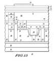
FIG. 13 issemiconductor device 10 wherein the second plate electrodeconductive material 79 is formed as a result of a conventional etch process. - Illustrated in
FIG. 14 issemiconductor device 10 wherein anitride layer 83 is formed overlying the top of the second plate electrodeconductive material 79 as an etch stop layer.Photoresist 85 defines the first electrode layer pattern. - As illustrated in
FIG. 15 , the pattern ofphotoresist 85 is transferred into thelayers conductive material 75. The pattern may be transferred using a conventional dry etch or wet etch or a combination thereof and is selective to the etch stop orbarrier layer 72.Photoresist 81 is removed from thesemiconductor device 10. Asubsequent oxide film 87 that functions as an insulating layer is deposited and planarized (in one form, a polish) to form a planar upper surface. Ahard mask layer 89 is formed overlying theoxide film 87. Aphotoresist 91 defines via openings for thesemiconductor device 10 for contact to the first and second capacitor plates in addition toconductive material 68. It should be noted that the capacitor formed by the metal structure orconductive material 75, the insulatinglayer 77, and the metal structure orconductive material 79 has at least a portion of which is located on a line that is orthogonal to the surface ofactive layer 16 and through the active device (transistor formed bygate 18,source region 22 and drain region23). It should be understood thatsource region 22 and drainregion 23 may be implemented as either a source/drain region or a drain/source region depending upon conductivity doping. - As illustrated in
FIG. 16 , the via openings are etched in the form of a through contact via113, a topside electrode via93, a bottom side electrode via95 and a via96.Photoresist 97 defines metal openings.Layer 89 acts as an antireflective coating (ARC) material or as a hard mask material similar tolayer 62. - As illustrated in
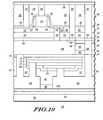
FIG. 17 , the pattern defined byphotoresist 97 is transferred intolayer 89 andoxide film 87. The pattern transfer, in one form, may be implemented with either conventional dry or wet etching techniques. Openings are filled with aconductive material 99 that functions as a second metal structure by using conventional deposition techniques. In one form, theconductive material 99 is a metal and forms a metal structure. In one form,conductive material 99 may be implemented with copper, silver, tungsten, nickel, gold, aluminum and alloys thereof, as well as other metals. It should be apparent thatconductive material 99 in the regions illustrated may be formed using conventional dual in-laid patterning, etch, fill and planarization techniques similar toFIG. 11 . InFIG. 17 a passivation layer90 is deposited onconductive material 99 andlayer 89. In one form, the passivation layer90 may be a carbide, nitride, oxide material or other dielectric materials. - In this embodiment, an active device in the form of a transistor is formed by
polysilicon gate 18 and the associated gate oxide (not shown),backside source region 22 and drainregion 23. Assume that in addition to the transistor illustrated, novel structures such as FinFETs or vertical transistors may be used in lieu of a conventional MOSFET. Directly underneath the active device (i.e. the illustrated transistor) is formed a passive device in the form of a capacitive element that functions in one application as a decoupling capacitor. A portion of the decoupling capacitor is positioned along a line that runs through any portion of the transistor wherein the line is orthogonal to a surface ofactive layer 16. - Illustrated in
FIG. 18 issemiconductor device 10 wherein afinal substrate 94 is joined to apassivation layer 101 through abonding layer 92. It should be understood that multiple conductive layers (not shown) may separate the conductive material88 and thepassivation layer 101. In addition,bonding layer 92 andfinal substrate 94 may be eliminated and replaced by multiple conductive layers (not shown) to form a conductive bump structure. In such an embodiment, thecarrier substrate 38 is the final substrate. - Illustrated in
FIG. 19 issemiconductor device 10 wherein thecarrier substrate 38 and thebonding layer 36 is removed. This removal process may include conventional techniques such as grinding, chemical mechanical polish (CMP), wet or dry etching selective to theetch stop layer 34. In addition, this removal process may include non-contact removal techniques such as laser lift-off, decomposition of the adhesive material, decomposition of bonds, etc.Final substrate 94 therefore becomes a final substrate forsemiconductor device 10. Further processing for metal layer formation and C4 attachment may be implemented pursuant to conventional processing techniques. - By now it should be appreciated that there has been provided a method for forming a semiconductor device wherein a passive device is formed directly beneath an active device. In the illustrated form, the passive device is implemented as a capacitor formed by
conductive material 75 andconductive material 79 as first and second plate electrodes, respectively, andlayer 73 as the intervening dielectric.Conductive material 79 of the capacitor is contacted to the front side by the interconnect formed byconductive material conductive regions 54 and one ofbackside contacts 32.Conductive material 75 of the capacitor is also connected to the transistor (i.e. the active device) byconductive material conductive region 52 to thebackside source region 22. Additionally,conductive material 68 may be implemented as an efficient power plane across a semiconductor die to distribute a power supply voltage across thesemiconductor device 10. The power plane would provide direct power to the transistor without having a lateral power plane that would consume circuit layout area. Additionally, the power plane ofconductive material 68 may be used to provide a back bias for the overlying transistor and change the transistor characteristics by applying a predetermined bias to the power plane. In such an implementation,conductive region 52 is not connected to the power plane being used to provide this bias. This bias modifies the depletion region of the transistor. Control of the biasing may be implemented so that sections of transistors within an integrated circuit may be biased by such a power plane for a predetermined type of circuit operation or during certain periods of operation, such as for example a period dependent upon the amount of power being consumed. - In the foregoing specification, the invention has been described with reference to specific embodiments. However, one of ordinary skill in the art appreciates that various modifications and changes can be made without departing from the scope of the present invention as set forth in the claims below. For example, any type of active device other than a transistor may be implemented such as diodes, photodetectors, MEM (micro electro mechanical) devices and optical sources. Various transistor structures that have a diffusion region may be implemented. Any type of passive device other than a capacitor may be implemented, such as resistors, inductors, waveguides, cavities, optical interconnects, optical components, couplers, heat dissipation elements and heat sinks. Any type of packaging interconnects may be incorporated with
semiconductor device 10 both at the front-side and the back-side. Various materials other than the specific examples described herein may be used for the conductors and insulators described herein. Accordingly, the specification and figures are to be regarded in an illustrative rather than a restrictive sense, and all such modifications are intended to be included within the scope of the present invention. - Benefits, other advantages, and solutions to problems have been described above with regard to specific embodiments. However, the benefits, advantages, solutions to problems, and any element(s) that may cause any benefit, advantage, or solution to occur or become more pronounced are not to be construed as a critical, required, or essential feature or element of any or all the claims. As used herein, the terms “comprises,” “comprising,” or any other variation thereof, are intended to cover a non-exclusive inclusion, such that a process, method, article, or apparatus that comprises a list of elements does not include only those elements but may include other elements not expressly listed or inherent to such process, method, article, or apparatus.
Claims (20)
Priority Applications (2)
| Application Number | Priority Date | Filing Date | Title |
|---|---|---|---|
| US10/946,758US6921961B2 (en) | 2003-08-15 | 2004-09-22 | Semiconductor device having electrical contact from opposite sides including a via with an end formed at a bottom surface of the diffusion region |
| US11/098,070US7122421B2 (en) | 2003-08-15 | 2005-04-04 | Semiconductor device including a transistor and a capacitor having an aligned transistor and capacitive element |
Applications Claiming Priority (2)
| Application Number | Priority Date | Filing Date | Title |
|---|---|---|---|
| US10/641,544US6838332B1 (en) | 2003-08-15 | 2003-08-15 | Method for forming a semiconductor device having electrical contact from opposite sides |
| US10/946,758US6921961B2 (en) | 2003-08-15 | 2004-09-22 | Semiconductor device having electrical contact from opposite sides including a via with an end formed at a bottom surface of the diffusion region |
Related Parent Applications (1)
| Application Number | Title | Priority Date | Filing Date |
|---|---|---|---|
| US10/641,544DivisionUS6838332B1 (en) | 2003-08-15 | 2003-08-15 | Method for forming a semiconductor device having electrical contact from opposite sides |
Related Child Applications (1)
| Application Number | Title | Priority Date | Filing Date |
|---|---|---|---|
| US11/098,070DivisionUS7122421B2 (en) | 2003-08-15 | 2005-04-04 | Semiconductor device including a transistor and a capacitor having an aligned transistor and capacitive element |
Publications (2)
| Publication Number | Publication Date |
|---|---|
| US20050042867A1true US20050042867A1 (en) | 2005-02-24 |
| US6921961B2 US6921961B2 (en) | 2005-07-26 |
Family
ID=33541573
Family Applications (3)
| Application Number | Title | Priority Date | Filing Date |
|---|---|---|---|
| US10/641,544Expired - LifetimeUS6838332B1 (en) | 2003-08-15 | 2003-08-15 | Method for forming a semiconductor device having electrical contact from opposite sides |
| US10/946,758Expired - LifetimeUS6921961B2 (en) | 2003-08-15 | 2004-09-22 | Semiconductor device having electrical contact from opposite sides including a via with an end formed at a bottom surface of the diffusion region |
| US11/098,070Expired - Fee RelatedUS7122421B2 (en) | 2003-08-15 | 2005-04-04 | Semiconductor device including a transistor and a capacitor having an aligned transistor and capacitive element |
Family Applications Before (1)
| Application Number | Title | Priority Date | Filing Date |
|---|---|---|---|
| US10/641,544Expired - LifetimeUS6838332B1 (en) | 2003-08-15 | 2003-08-15 | Method for forming a semiconductor device having electrical contact from opposite sides |
Family Applications After (1)
| Application Number | Title | Priority Date | Filing Date |
|---|---|---|---|
| US11/098,070Expired - Fee RelatedUS7122421B2 (en) | 2003-08-15 | 2005-04-04 | Semiconductor device including a transistor and a capacitor having an aligned transistor and capacitive element |
Country Status (6)
| Country | Link |
|---|---|
| US (3) | US6838332B1 (en) |
| EP (1) | EP1656698A4 (en) |
| JP (1) | JP2007521659A (en) |
| CN (1) | CN100362650C (en) |
| TW (1) | TWI344191B (en) |
| WO (1) | WO2005020279A2 (en) |
Cited By (15)
| Publication number | Priority date | Publication date | Assignee | Title |
|---|---|---|---|---|
| US20070122975A1 (en)* | 2005-11-28 | 2007-05-31 | Stmicroelectronics Crolles 2 Sas | MOS transistor manufacturing |
| US20080128812A1 (en)* | 2006-05-16 | 2008-06-05 | Kerry Bernstein | Dual wired integrated circuit chips |
| US20080217705A1 (en)* | 2007-03-08 | 2008-09-11 | Hall Mark D | Trench formation in a semiconductor material |
| US20090001598A1 (en)* | 2007-06-27 | 2009-01-01 | Wen-Chih Chiou | Formation of Through Via before Contact Processing |
| US20090121287A1 (en)* | 2007-11-14 | 2009-05-14 | Kerry Bernstein | Dual wired integrated circuit chips |
| US20090224371A1 (en)* | 2008-03-05 | 2009-09-10 | Chen-Hua Yu | Protection for Bonding Pads and Methods of Formation |
| US20090286346A1 (en)* | 2008-05-14 | 2009-11-19 | International Business Machines Corporation | Methods For Forming Anti-Reflection Structures For CMOS Image Sensors |
| US20090283871A1 (en)* | 2008-05-14 | 2009-11-19 | Hung-Pin Chang | System, Structure, and Method of Manufacturing a Semiconductor Substrate Stack |
| US20100267217A1 (en)* | 2009-04-20 | 2010-10-21 | Taiwan Semiconductor Manufacturing Company, Ltd. | Backside Process for a Substrate |
| US20100264473A1 (en)* | 2008-05-14 | 2010-10-21 | International Business Machines Corporation | Anti-reflection structures for cmos image sensors |
| US20110169082A1 (en)* | 2010-01-14 | 2011-07-14 | International Business Machines Corporation | Method for forming retrograded well for mosfet |
| DE102011013228A1 (en)* | 2011-03-07 | 2012-09-13 | Austriamicrosystems Ag | Method for manufacturing semiconductor component that is three-dimensionally integrated in semiconductor chip stack, involves selectively removing upper stop layer with respect to lower stop layer |
| US20180083134A1 (en)* | 2016-04-06 | 2018-03-22 | International Business Machines Corporation | Bulk to silicon on insulator device |
| US11264493B2 (en)* | 2015-09-25 | 2022-03-01 | Intel Corporation | Wrap-around source/drain method of making contacts for backside metals |
| US20230420366A1 (en)* | 2022-06-22 | 2023-12-28 | International Business Machines Corporation | Power planes and pass-through vias |
Families Citing this family (48)
| Publication number | Priority date | Publication date | Assignee | Title |
|---|---|---|---|---|
| JP4152352B2 (en)* | 2004-06-17 | 2008-09-17 | 松下電器産業株式会社 | Optical semiconductor device and manufacturing method thereof |
| US7064043B1 (en)* | 2004-12-09 | 2006-06-20 | Texas Instruments Incorporated | Wafer bonded MOS decoupling capacitor |
| US7253083B2 (en)* | 2005-06-17 | 2007-08-07 | Northrop Grumman Corporation | Method of thinning a semiconductor structure |
| US7345344B2 (en)* | 2006-02-16 | 2008-03-18 | Freescale Semiconductor, Inc. | Embedded substrate interconnect for underside contact to source and drain regions |
| US7402477B2 (en)* | 2006-03-30 | 2008-07-22 | Freescale Semiconductor, Inc. | Method of making a multiple crystal orientation semiconductor device |
| US7473979B2 (en)* | 2006-05-30 | 2009-01-06 | International Business Machines Corporation | Semiconductor integrated circuit devices having high-Q wafer back-side capacitors |
| US7772701B2 (en)* | 2006-06-07 | 2010-08-10 | Taiwan Semiconductor Manufacturing Co., Ltd. | Integrated circuit having improved interconnect structure |
| US7402866B2 (en)* | 2006-06-27 | 2008-07-22 | Taiwan Semiconductor Manufacturing Company, Ltd. | Backside contacts for MOS devices |
| JP4956128B2 (en)* | 2006-10-02 | 2012-06-20 | ルネサスエレクトロニクス株式会社 | Manufacturing method of electronic device |
| US7485508B2 (en)* | 2007-01-26 | 2009-02-03 | International Business Machines Corporation | Two-sided semiconductor-on-insulator structures and methods of manufacturing the same |
| FR2910704A1 (en)* | 2007-04-05 | 2008-06-27 | Commissariat Energie Atomique | Interconnected integrated circuit device e.g. dynamic D flip-flop, forming method for electronic component, involves forming set of interconnection layers connected to semiconductor device and another set of layers, on active layer surface |
| US8299583B2 (en)* | 2009-03-05 | 2012-10-30 | International Business Machines Corporation | Two-sided semiconductor structure |
| US8604590B2 (en)* | 2009-04-30 | 2013-12-10 | Sony Corporation | Transistor with enhanced capacitance at electrodes and transistor with light emitting capacitive element |
| US8674468B2 (en)* | 2009-05-29 | 2014-03-18 | Carestream Health, Inc. | Imaging array with dual height semiconductor and method of making same |
| US7948017B2 (en)* | 2009-06-19 | 2011-05-24 | Carestream Health, Inc. | Digital radiography imager with buried interconnect layer in silicon-on-glass and method of fabricating same |
| US8105887B2 (en) | 2009-07-09 | 2012-01-31 | International Business Machines Corporation | Inducing stress in CMOS device |
| US7968358B2 (en)* | 2009-07-29 | 2011-06-28 | Carestream Health, Inc. | Digital radiographic flat-panel imaging array with dual height semiconductor and method of making same |
| IT1398204B1 (en) | 2010-02-16 | 2013-02-14 | St Microelectronics Srl | SYSTEM AND METHOD TO PERFORM THE ELECTRIC TEST OF THROUGH THE SILICON (TSV - THROUGH SILICON VIAS). |
| US8525342B2 (en) | 2010-04-12 | 2013-09-03 | Qualcomm Incorporated | Dual-side interconnected CMOS for stacked integrated circuits |
| US20110254092A1 (en)* | 2010-04-14 | 2011-10-20 | Globalfoundries Inc. | Etsoi cmos architecture with dual backside stressors |
| US8405036B2 (en) | 2010-08-24 | 2013-03-26 | Carestream Health, Inc. | Digital radiography imager with buried interconnect layer in silicon-on-glass and method of fabricating same |
| US9947688B2 (en)* | 2011-06-22 | 2018-04-17 | Psemi Corporation | Integrated circuits with components on both sides of a selected substrate and methods of fabrication |
| US8648438B2 (en) | 2011-10-03 | 2014-02-11 | International Business Machines Corporation | Structure and method to form passive devices in ETSOI process flow |
| TWI529939B (en)* | 2012-02-08 | 2016-04-11 | Sony Corp | High frequency semiconductor device and its manufacturing method |
| JP5661707B2 (en)* | 2012-09-18 | 2015-01-28 | ウィン セミコンダクターズ コーポレーション | Compound semiconductor integrated circuit |
| JP6292049B2 (en)* | 2013-09-02 | 2018-03-14 | ソニー株式会社 | Semiconductor device and manufacturing method thereof |
| CN104795354A (en)* | 2014-01-17 | 2015-07-22 | 中芯国际集成电路制造(上海)有限公司 | Chip integration method |
| US9343369B2 (en)* | 2014-05-19 | 2016-05-17 | Qualcomm Incorporated | Three dimensional (3D) integrated circuits (ICs) (3DICs) and related systems |
| CN105097770B (en)* | 2015-06-12 | 2019-02-15 | 武汉新芯集成电路制造有限公司 | Device architecture of three dimensional integrated circuits and preparation method thereof |
| CN105097769B (en)* | 2015-06-12 | 2018-03-02 | 武汉新芯集成电路制造有限公司 | A kind of device of three dimensional integrated circuits and preparation method thereof |
| US11296197B2 (en)* | 2015-09-25 | 2022-04-05 | Intel Corporation | Power gate with metal on both sides |
| US10473853B2 (en)* | 2016-12-22 | 2019-11-12 | Sifotonics Technologies Co., Ltd. | Fully integrated avalanche photodiode receiver |
| US9966318B1 (en)* | 2017-01-31 | 2018-05-08 | Stmicroelectronics S.R.L. | System for electrical testing of through silicon vias (TSVs) |
| CN107644839B (en)* | 2017-08-31 | 2018-10-02 | 长江存储科技有限责任公司 | Wafer three-dimensional integration lead technique and its structure for three-dimensional storage |
| US10679941B2 (en) | 2017-08-31 | 2020-06-09 | Yangtze Memory Technologies Co., Ltd. | Method for forming three-dimensional integrated wiring structure and semiconductor structure thereof |
| EP3667733A1 (en) | 2018-12-13 | 2020-06-17 | IMEC vzw | Silicided fin junction for back-side connection |
| CN111696961B (en) | 2019-03-11 | 2022-04-12 | 联华电子股份有限公司 | Semiconductor structure and manufacturing method thereof |
| KR102801648B1 (en) | 2019-05-21 | 2025-05-02 | 삼성전자주식회사 | Semiconductor device |
| DE102020123277A1 (en)* | 2019-12-29 | 2021-07-01 | Taiwan Semiconductor Manufacturing Co., Ltd. | STRUCTURE AND PROCEDURE FOR TRANSISTORS THAT HAVE REAR BUSBARS |
| US11532556B2 (en)* | 2019-12-29 | 2022-12-20 | Taiwan Semiconductor Manufacturing Co., Ltd. | Structure and method for transistors having backside power rails |
| KR102524729B1 (en)* | 2019-12-29 | 2023-04-21 | 타이완 세미콘덕터 매뉴팩쳐링 컴퍼니 리미티드 | Structure and method for transistors having backside power rails |
| US11081559B1 (en)* | 2020-01-31 | 2021-08-03 | Qualcomm Incorporated | Backside contact of a semiconductor device |
| US11239325B2 (en)* | 2020-04-28 | 2022-02-01 | Taiwan Semiconductor Manufacturing Co., Ltd. | Semiconductor device having backside via and method of fabricating thereof |
| US11417767B2 (en)* | 2020-05-27 | 2022-08-16 | Taiwan Semiconductor Manufacturing Co., Ltd. | Semiconductor devices including backside vias and methods of forming the same |
| DE102020122828B4 (en)* | 2020-05-27 | 2022-08-11 | Taiwan Semiconductor Manufacturing Co., Ltd. | SEMICONDUCTOR DEVICES HAVING BACK VIA THRU-PHONES AND METHOD OF FORMING SAME |
| US11799002B2 (en)* | 2020-05-29 | 2023-10-24 | Taiwan Semiconductor Manufacturing Co., Ltd. | Semiconductor devices and methods of forming the same |
| US12165973B2 (en)* | 2020-09-30 | 2024-12-10 | Taiwan Semiconductor Manufacturing Company, Ltd. | Semiconductor device with backside power rail and method for forming the same |
| US12412836B2 (en)* | 2022-05-11 | 2025-09-09 | International Business Machines Corporation | Backside power plane |
Citations (9)
| Publication number | Priority date | Publication date | Assignee | Title |
|---|---|---|---|---|
| US5378914A (en)* | 1990-05-31 | 1995-01-03 | Canon Kabushiki Kaisha | Semiconductor device with a particular source/drain and gate structure |
| US5426072A (en)* | 1993-01-21 | 1995-06-20 | Hughes Aircraft Company | Process of manufacturing a three dimensional integrated circuit from stacked SOI wafers using a temporary silicon substrate |
| US5473181A (en)* | 1993-11-05 | 1995-12-05 | Siemens Aktiengesellschaft | Integrated circuit arrangement having at least one power component and low-voltage components |
| US5614743A (en)* | 1994-07-26 | 1997-03-25 | Kabushiki Kaisha Toshiba | Microwave integrated circuit (MIC) having a reactance element formed on a groove |
| US5949140A (en)* | 1996-05-30 | 1999-09-07 | Oki Electric Industry Co., Ltd. | Microwave semiconductor device with via holes and associated structure |
| US6355501B1 (en)* | 2000-09-21 | 2002-03-12 | International Business Machines Corporation | Three-dimensional chip stacking assembly |
| US6358828B1 (en)* | 1997-06-20 | 2002-03-19 | Advanced Micro Devices, Inc. | Ultra high density series-connected transistors formed on separate elevational levels |
| US6500724B1 (en)* | 2000-08-21 | 2002-12-31 | Motorola, Inc. | Method of making semiconductor device having passive elements including forming capacitor electrode and resistor from same layer of material |
| US6525300B1 (en)* | 1999-07-30 | 2003-02-25 | Schott Glas | Cooking surface for cooking food having a glass ceramic surface with a glass coating thereon |
Family Cites Families (6)
| Publication number | Priority date | Publication date | Assignee | Title |
|---|---|---|---|---|
| TW214603B (en)* | 1992-05-13 | 1993-10-11 | Seiko Electron Co Ltd | Semiconductor device |
| US5843820A (en)* | 1997-09-29 | 1998-12-01 | Vanguard International Semiconductor Corporation | Method of fabricating a new dynamic random access memory (DRAM) cell having a buried horizontal trench capacitor |
| US6037822A (en)* | 1997-09-30 | 2000-03-14 | Intel Corporation | Method and apparatus for distributing a clock on the silicon backside of an integrated circuit |
| TW442873B (en) | 1999-01-14 | 2001-06-23 | United Microelectronics Corp | Three-dimension stack-type chip structure and its manufacturing method |
| KR100335778B1 (en)* | 1999-04-08 | 2002-05-09 | 박종섭 | Semiconductor device and a method of manufacturing thereof |
| JP3462166B2 (en)* | 2000-09-08 | 2003-11-05 | 富士通カンタムデバイス株式会社 | Compound semiconductor device |
- 2003
- 2003-08-15USUS10/641,544patent/US6838332B1/ennot_activeExpired - Lifetime
- 2004
- 2004-07-13CNCNB2004800204840Apatent/CN100362650C/ennot_activeExpired - Fee Related
- 2004-07-13EPEP04778110Apatent/EP1656698A4/ennot_activeWithdrawn
- 2004-07-13WOPCT/US2004/022437patent/WO2005020279A2/ennot_activeApplication Discontinuation
- 2004-07-13JPJP2006523196Apatent/JP2007521659A/enactivePending
- 2004-08-02TWTW093123127Apatent/TWI344191B/ennot_activeIP Right Cessation
- 2004-09-22USUS10/946,758patent/US6921961B2/ennot_activeExpired - Lifetime
- 2005
- 2005-04-04USUS11/098,070patent/US7122421B2/ennot_activeExpired - Fee Related
Patent Citations (9)
| Publication number | Priority date | Publication date | Assignee | Title |
|---|---|---|---|---|
| US5378914A (en)* | 1990-05-31 | 1995-01-03 | Canon Kabushiki Kaisha | Semiconductor device with a particular source/drain and gate structure |
| US5426072A (en)* | 1993-01-21 | 1995-06-20 | Hughes Aircraft Company | Process of manufacturing a three dimensional integrated circuit from stacked SOI wafers using a temporary silicon substrate |
| US5473181A (en)* | 1993-11-05 | 1995-12-05 | Siemens Aktiengesellschaft | Integrated circuit arrangement having at least one power component and low-voltage components |
| US5614743A (en)* | 1994-07-26 | 1997-03-25 | Kabushiki Kaisha Toshiba | Microwave integrated circuit (MIC) having a reactance element formed on a groove |
| US5949140A (en)* | 1996-05-30 | 1999-09-07 | Oki Electric Industry Co., Ltd. | Microwave semiconductor device with via holes and associated structure |
| US6358828B1 (en)* | 1997-06-20 | 2002-03-19 | Advanced Micro Devices, Inc. | Ultra high density series-connected transistors formed on separate elevational levels |
| US6525300B1 (en)* | 1999-07-30 | 2003-02-25 | Schott Glas | Cooking surface for cooking food having a glass ceramic surface with a glass coating thereon |
| US6500724B1 (en)* | 2000-08-21 | 2002-12-31 | Motorola, Inc. | Method of making semiconductor device having passive elements including forming capacitor electrode and resistor from same layer of material |
| US6355501B1 (en)* | 2000-09-21 | 2002-03-12 | International Business Machines Corporation | Three-dimensional chip stacking assembly |
Cited By (46)
| Publication number | Priority date | Publication date | Assignee | Title |
|---|---|---|---|---|
| US20070122975A1 (en)* | 2005-11-28 | 2007-05-31 | Stmicroelectronics Crolles 2 Sas | MOS transistor manufacturing |
| US7556995B2 (en) | 2005-11-28 | 2009-07-07 | Stmicroelectronics Crolles 2 Sas | MOS transistor manufacturing |
| US20090224295A1 (en)* | 2005-11-28 | 2009-09-10 | Stmicroelectronics (Crolles) 2 Sas | Mos transistor manufacturing |
| US7915110B2 (en) | 2005-11-28 | 2011-03-29 | Stmicroelectronics (Crolles 2) Sas | MOS transistor manufacturing |
| US20080128812A1 (en)* | 2006-05-16 | 2008-06-05 | Kerry Bernstein | Dual wired integrated circuit chips |
| US20080213948A1 (en)* | 2006-05-16 | 2008-09-04 | Kerry Bernstein | Dual wired integrated circuit chips |
| US7960245B2 (en) | 2006-05-16 | 2011-06-14 | International Business Machines Corporation | Dual wired integrated circuit chips |
| US7939914B2 (en)* | 2006-05-16 | 2011-05-10 | International Business Machines Corporation | Dual wired integrated circuit chips |
| KR101055711B1 (en) | 2006-05-16 | 2011-08-11 | 인터내셔널 비지네스 머신즈 코포레이션 | Dual-wired integrated circuit chips |
| US20080217705A1 (en)* | 2007-03-08 | 2008-09-11 | Hall Mark D | Trench formation in a semiconductor material |
| US7879663B2 (en)* | 2007-03-08 | 2011-02-01 | Freescale Semiconductor, Inc. | Trench formation in a semiconductor material |
| US20090001598A1 (en)* | 2007-06-27 | 2009-01-01 | Wen-Chih Chiou | Formation of Through Via before Contact Processing |
| US9209157B2 (en) | 2007-06-27 | 2015-12-08 | Taiwan Semiconductor Manufacturing Company, Ltd. | Formation of through via before contact processing |
| US9793192B2 (en) | 2007-06-27 | 2017-10-17 | Taiwan Semiconductor Manufacturing Company, Ltd. | Formation of through via before contact processing |
| US7939941B2 (en)* | 2007-06-27 | 2011-05-10 | Taiwan Semiconductor Manufacturing Company, Ltd. | Formation of through via before contact processing |
| US20110177655A1 (en)* | 2007-06-27 | 2011-07-21 | Taiwan Semiconductor Manufacturing Company, Ltd. | Formation of Through Via before Contact Processing |
| US20090121287A1 (en)* | 2007-11-14 | 2009-05-14 | Kerry Bernstein | Dual wired integrated circuit chips |
| US7872357B2 (en) | 2008-03-05 | 2011-01-18 | Taiwan Semiconductor Manufacturing Company, Ltd. | Protection for bonding pads and methods of formation |
| US20090224371A1 (en)* | 2008-03-05 | 2009-09-10 | Chen-Hua Yu | Protection for Bonding Pads and Methods of Formation |
| US8003425B2 (en)* | 2008-05-14 | 2011-08-23 | International Business Machines Corporation | Methods for forming anti-reflection structures for CMOS image sensors |
| US8853830B2 (en) | 2008-05-14 | 2014-10-07 | Taiwan Semiconductor Manufacturing Company, Ltd. | System, structure, and method of manufacturing a semiconductor substrate stack |
| US20100264473A1 (en)* | 2008-05-14 | 2010-10-21 | International Business Machines Corporation | Anti-reflection structures for cmos image sensors |
| US11004832B2 (en) | 2008-05-14 | 2021-05-11 | Taiwan Semiconductor Manufacturing Company, Ltd. | System, structure, and method of manufacturing a semiconductor substrate stack |
| US8138534B2 (en) | 2008-05-14 | 2012-03-20 | International Business Machines Corporation | Anti-reflection structures for CMOS image sensors |
| US10515933B2 (en) | 2008-05-14 | 2019-12-24 | Taiwan Semiconductor Manufacturing Company, Ltd. | System, structure, and method of manufacturing a semiconductor substrate stack |
| US20090286346A1 (en)* | 2008-05-14 | 2009-11-19 | International Business Machines Corporation | Methods For Forming Anti-Reflection Structures For CMOS Image Sensors |
| US8409904B2 (en) | 2008-05-14 | 2013-04-02 | International Business Machines Corporation | Methods for forming anti-reflection structures for CMOS image sensors |
| US9728457B2 (en) | 2008-05-14 | 2017-08-08 | Taiwan Semiconductor Manufacturing Company, Ltd. | System, structure, and method of manufacturing a semiconductor substrate stack |
| US20090283871A1 (en)* | 2008-05-14 | 2009-11-19 | Hung-Pin Chang | System, Structure, and Method of Manufacturing a Semiconductor Substrate Stack |
| US8716771B2 (en) | 2008-05-14 | 2014-05-06 | International Business Machines Corporation | Anti-reflection structures for CMOS image sensors |
| US8742560B2 (en) | 2008-05-14 | 2014-06-03 | International Business Machines Corporation | Anti-reflection structures for CMOS image sensors |
| US20100267217A1 (en)* | 2009-04-20 | 2010-10-21 | Taiwan Semiconductor Manufacturing Company, Ltd. | Backside Process for a Substrate |
| US8691664B2 (en) | 2009-04-20 | 2014-04-08 | Taiwan Semiconductor Manufacturing Company, Ltd. | Backside process for a substrate |
| US20110169082A1 (en)* | 2010-01-14 | 2011-07-14 | International Business Machines Corporation | Method for forming retrograded well for mosfet |
| US8492842B2 (en) | 2010-01-14 | 2013-07-23 | International Business Machines Corporation | Method for forming retrograded well for MOSFET |
| US8343818B2 (en)* | 2010-01-14 | 2013-01-01 | International Business Machines Corporation | Method for forming retrograded well for MOSFET |
| DE102011013228B4 (en)* | 2011-03-07 | 2014-05-28 | Austriamicrosystems Ag | Method of manufacturing a semiconductor device for 3D integration |
| DE102011013228A1 (en)* | 2011-03-07 | 2012-09-13 | Austriamicrosystems Ag | Method for manufacturing semiconductor component that is three-dimensionally integrated in semiconductor chip stack, involves selectively removing upper stop layer with respect to lower stop layer |
| US12100762B2 (en) | 2015-09-25 | 2024-09-24 | Intel Corporation | Wrap-around source/drain method of making contacts for backside metals |
| US12100761B2 (en) | 2015-09-25 | 2024-09-24 | Intel Corporation | Wrap-around source/drain method of making contacts for backside metals |
| US11264493B2 (en)* | 2015-09-25 | 2022-03-01 | Intel Corporation | Wrap-around source/drain method of making contacts for backside metals |
| US9991339B2 (en)* | 2016-04-06 | 2018-06-05 | International Business Machines Corporation | Bulk to silicon on insulator device |
| US10608080B2 (en)* | 2016-04-06 | 2020-03-31 | International Business Machines Corporation | Bulk to silicon on insulator device |
| US10332959B2 (en)* | 2016-04-06 | 2019-06-25 | International Business Machines Corporation | Bulk to silicon on insulator device |
| US20180083134A1 (en)* | 2016-04-06 | 2018-03-22 | International Business Machines Corporation | Bulk to silicon on insulator device |
| US20230420366A1 (en)* | 2022-06-22 | 2023-12-28 | International Business Machines Corporation | Power planes and pass-through vias |
Also Published As
| Publication number | Publication date |
|---|---|
| JP2007521659A (en) | 2007-08-02 |
| TWI344191B (en) | 2011-06-21 |
| US6838332B1 (en) | 2005-01-04 |
| WO2005020279A2 (en) | 2005-03-03 |
| US7122421B2 (en) | 2006-10-17 |
| CN1823413A (en) | 2006-08-23 |
| TW200511500A (en) | 2005-03-16 |
| WO2005020279A3 (en) | 2005-07-21 |
| EP1656698A4 (en) | 2007-07-04 |
| US6921961B2 (en) | 2005-07-26 |
| US20050167782A1 (en) | 2005-08-04 |
| CN100362650C (en) | 2008-01-16 |
| EP1656698A2 (en) | 2006-05-17 |
Similar Documents
| Publication | Publication Date | Title |
|---|---|---|
| US6921961B2 (en) | Semiconductor device having electrical contact from opposite sides including a via with an end formed at a bottom surface of the diffusion region | |
| US7704811B2 (en) | Sub-lithographics opening for back contact or back gate | |
| KR100562241B1 (en) | Thermal conductivity enhanced semiconductor structures and fabrication processes | |
| KR100243658B1 (en) | Inductor device using substrate biasing technigue and method for fabricating the same | |
| EP3203507B1 (en) | Semiconductor structure and fabrication method thereof | |
| US7326642B2 (en) | Method of fabricating semiconductor device using low dielectric constant material film | |
| US9466536B2 (en) | Semiconductor-on-insulator integrated circuit with back side gate | |
| US5753529A (en) | Surface mount and flip chip technology for total integrated circuit isolation | |
| JP5048230B2 (en) | Semiconductor device and manufacturing method thereof | |
| KR100323488B1 (en) | Contact structure for vertical chip connection | |
| US20080142923A1 (en) | Semiconductor structure and method of manufacture | |
| TW201606995A (en) | Columnar resistor structure for integrated circuit | |
| JP2004111634A (en) | Semiconductor device and method of manufacturing semiconductor device | |
| CN222532107U (en) | Semiconductor components and semiconductor chips | |
| US7189602B2 (en) | Method and apparatus for reducing substrate bias voltage drop | |
| US9620643B2 (en) | Reducing parasitic capacitance and resistance in finFET | |
| US20250072113A1 (en) | Stacked FET With Local Contact | |
| WO2006070309A1 (en) | Semiconductor device having strip- shaped channel and method for manufacturing such a device | |
| CN115863261A (en) | Semiconductor structures and methods of forming them | |
| JPH1027912A (en) | Structure of electrode buried within layer and formation thereof | |
| KR20000053544A (en) | An integrated circuit device having an internal top to bottom conductive path |
Legal Events
| Date | Code | Title | Description |
|---|---|---|---|
| STCF | Information on status: patent grant | Free format text:PATENTED CASE | |
| AS | Assignment | Owner name:CITIBANK, N.A. AS COLLATERAL AGENT, NEW YORK Free format text:SECURITY AGREEMENT;ASSIGNORS:FREESCALE SEMICONDUCTOR, INC.;FREESCALE ACQUISITION CORPORATION;FREESCALE ACQUISITION HOLDINGS CORP.;AND OTHERS;REEL/FRAME:018855/0129 Effective date:20061201 Owner name:CITIBANK, N.A. AS COLLATERAL AGENT,NEW YORK Free format text:SECURITY AGREEMENT;ASSIGNORS:FREESCALE SEMICONDUCTOR, INC.;FREESCALE ACQUISITION CORPORATION;FREESCALE ACQUISITION HOLDINGS CORP.;AND OTHERS;REEL/FRAME:018855/0129 Effective date:20061201 | |
| FPAY | Fee payment | Year of fee payment:4 | |
| AS | Assignment | Owner name:CITIBANK, N.A., AS COLLATERAL AGENT,NEW YORK Free format text:SECURITY AGREEMENT;ASSIGNOR:FREESCALE SEMICONDUCTOR, INC.;REEL/FRAME:024397/0001 Effective date:20100413 Owner name:CITIBANK, N.A., AS COLLATERAL AGENT, NEW YORK Free format text:SECURITY AGREEMENT;ASSIGNOR:FREESCALE SEMICONDUCTOR, INC.;REEL/FRAME:024397/0001 Effective date:20100413 | |
| FPAY | Fee payment | Year of fee payment:8 | |
| AS | Assignment | Owner name:CITIBANK, N.A., AS NOTES COLLATERAL AGENT, NEW YORK Free format text:SECURITY AGREEMENT;ASSIGNOR:FREESCALE SEMICONDUCTOR, INC.;REEL/FRAME:030633/0424 Effective date:20130521 Owner name:CITIBANK, N.A., AS NOTES COLLATERAL AGENT, NEW YOR Free format text:SECURITY AGREEMENT;ASSIGNOR:FREESCALE SEMICONDUCTOR, INC.;REEL/FRAME:030633/0424 Effective date:20130521 | |
| AS | Assignment | Owner name:CITIBANK, N.A., AS NOTES COLLATERAL AGENT, NEW YORK Free format text:SECURITY AGREEMENT;ASSIGNOR:FREESCALE SEMICONDUCTOR, INC.;REEL/FRAME:031591/0266 Effective date:20131101 Owner name:CITIBANK, N.A., AS NOTES COLLATERAL AGENT, NEW YOR Free format text:SECURITY AGREEMENT;ASSIGNOR:FREESCALE SEMICONDUCTOR, INC.;REEL/FRAME:031591/0266 Effective date:20131101 | |
| AS | Assignment | Owner name:FREESCALE SEMICONDUCTOR, INC., TEXAS Free format text:PATENT RELEASE;ASSIGNOR:CITIBANK, N.A., AS COLLATERAL AGENT;REEL/FRAME:037356/0143 Effective date:20151207 Owner name:FREESCALE SEMICONDUCTOR, INC., TEXAS Free format text:PATENT RELEASE;ASSIGNOR:CITIBANK, N.A., AS COLLATERAL AGENT;REEL/FRAME:037356/0553 Effective date:20151207 Owner name:FREESCALE SEMICONDUCTOR, INC., TEXAS Free format text:PATENT RELEASE;ASSIGNOR:CITIBANK, N.A., AS COLLATERAL AGENT;REEL/FRAME:037354/0225 Effective date:20151207 | |
| AS | Assignment | Owner name:MORGAN STANLEY SENIOR FUNDING, INC., MARYLAND Free format text:ASSIGNMENT AND ASSUMPTION OF SECURITY INTEREST IN PATENTS;ASSIGNOR:CITIBANK, N.A.;REEL/FRAME:037486/0517 Effective date:20151207 | |
| AS | Assignment | Owner name:MORGAN STANLEY SENIOR FUNDING, INC., MARYLAND Free format text:ASSIGNMENT AND ASSUMPTION OF SECURITY INTEREST IN PATENTS;ASSIGNOR:CITIBANK, N.A.;REEL/FRAME:037518/0292 Effective date:20151207 | |
| AS | Assignment | Owner name:NORTH STAR INNOVATIONS INC., CALIFORNIA Free format text:ASSIGNMENT OF ASSIGNORS INTEREST;ASSIGNOR:FREESCALE SEMICONDUCTOR, INC.;REEL/FRAME:037694/0264 Effective date:20151002 | |
| AS | Assignment | Owner name:NXP, B.V., F/K/A FREESCALE SEMICONDUCTOR, INC., NETHERLANDS Free format text:RELEASE BY SECURED PARTY;ASSIGNOR:MORGAN STANLEY SENIOR FUNDING, INC.;REEL/FRAME:040925/0001 Effective date:20160912 Owner name:NXP, B.V., F/K/A FREESCALE SEMICONDUCTOR, INC., NE Free format text:RELEASE BY SECURED PARTY;ASSIGNOR:MORGAN STANLEY SENIOR FUNDING, INC.;REEL/FRAME:040925/0001 Effective date:20160912 | |
| AS | Assignment | Owner name:NXP B.V., NETHERLANDS Free format text:RELEASE BY SECURED PARTY;ASSIGNOR:MORGAN STANLEY SENIOR FUNDING, INC.;REEL/FRAME:040928/0001 Effective date:20160622 | |
| FPAY | Fee payment | Year of fee payment:12 | |
| AS | Assignment | Owner name:MORGAN STANLEY SENIOR FUNDING, INC., MARYLAND Free format text:CORRECTIVE ASSIGNMENT TO CORRECT THE REMOVE PATENTS 8108266 AND 8062324 AND REPLACE THEM WITH 6108266 AND 8060324 PREVIOUSLY RECORDED ON REEL 037518 FRAME 0292. ASSIGNOR(S) HEREBY CONFIRMS THE ASSIGNMENT AND ASSUMPTION OF SECURITY INTEREST IN PATENTS;ASSIGNOR:CITIBANK, N.A.;REEL/FRAME:041703/0536 Effective date:20151207 | |
| AS | Assignment | Owner name:SHENZHEN XINGUODU TECHNOLOGY CO., LTD., CHINA Free format text:CORRECTIVE ASSIGNMENT TO CORRECT THE TO CORRECT THE APPLICATION NO. FROM 13,883,290 TO 13,833,290 PREVIOUSLY RECORDED ON REEL 041703 FRAME 0536. ASSIGNOR(S) HEREBY CONFIRMS THE THE ASSIGNMENT AND ASSUMPTION OF SECURITYINTEREST IN PATENTS.;ASSIGNOR:MORGAN STANLEY SENIOR FUNDING, INC.;REEL/FRAME:048734/0001 Effective date:20190217 | |
| AS | Assignment | Owner name:MORGAN STANLEY SENIOR FUNDING, INC., MARYLAND Free format text:CORRECTIVE ASSIGNMENT TO CORRECT THE REMOVE APPLICATION11759915 AND REPLACE IT WITH APPLICATION 11759935 PREVIOUSLY RECORDED ON REEL 037486 FRAME 0517. ASSIGNOR(S) HEREBY CONFIRMS THE ASSIGNMENT AND ASSUMPTION OF SECURITYINTEREST IN PATENTS;ASSIGNOR:CITIBANK, N.A.;REEL/FRAME:053547/0421 Effective date:20151207 | |
| AS | Assignment | Owner name:NXP B.V., NETHERLANDS Free format text:CORRECTIVE ASSIGNMENT TO CORRECT THE REMOVEAPPLICATION 11759915 AND REPLACE IT WITH APPLICATION11759935 PREVIOUSLY RECORDED ON REEL 040928 FRAME 0001. ASSIGNOR(S) HEREBY CONFIRMS THE RELEASE OF SECURITYINTEREST;ASSIGNOR:MORGAN STANLEY SENIOR FUNDING, INC.;REEL/FRAME:052915/0001 Effective date:20160622 | |
| AS | Assignment | Owner name:NXP, B.V. F/K/A FREESCALE SEMICONDUCTOR, INC., NETHERLANDS Free format text:CORRECTIVE ASSIGNMENT TO CORRECT THE REMOVEAPPLICATION 11759915 AND REPLACE IT WITH APPLICATION11759935 PREVIOUSLY RECORDED ON REEL 040925 FRAME 0001. ASSIGNOR(S) HEREBY CONFIRMS THE RELEASE OF SECURITYINTEREST;ASSIGNOR:MORGAN STANLEY SENIOR FUNDING, INC.;REEL/FRAME:052917/0001 Effective date:20160912 |