US20050042849A1 - Reacted conductive gate electrodes - Google Patents
Reacted conductive gate electrodesDownload PDFInfo
- Publication number
- US20050042849A1 US20050042849A1US10/944,618US94461804AUS2005042849A1US 20050042849 A1US20050042849 A1US 20050042849A1US 94461804 AUS94461804 AUS 94461804AUS 2005042849 A1US2005042849 A1US 2005042849A1
- Authority
- US
- United States
- Prior art keywords
- semiconductor device
- layer
- semiconductor
- silicon
- sige
- Prior art date
- Legal status (The legal status is an assumption and is not a legal conclusion. Google has not performed a legal analysis and makes no representation as to the accuracy of the status listed.)
- Granted
Links
- 239000004065semiconductorSubstances0.000claimsabstractdescription105
- 229910052710siliconInorganic materials0.000claimsabstractdescription63
- 239000010703siliconSubstances0.000claimsabstractdescription63
- 239000000463materialSubstances0.000claimsabstractdescription49
- 229910052732germaniumInorganic materials0.000claimsabstractdescription29
- GNPVGFCGXDBREM-UHFFFAOYSA-Ngermanium atomChemical compound[Ge]GNPVGFCGXDBREM-UHFFFAOYSA-N0.000claimsabstractdescription27
- 229910000577Silicon-germaniumInorganic materials0.000claimsdescription93
- 239000000758substrateSubstances0.000claimsdescription81
- XUIMIQQOPSSXEZ-UHFFFAOYSA-NSiliconChemical compound[Si]XUIMIQQOPSSXEZ-UHFFFAOYSA-N0.000claimsdescription56
- FVBUAEGBCNSCDD-UHFFFAOYSA-Nsilicide(4-)Chemical compound[Si-4]FVBUAEGBCNSCDD-UHFFFAOYSA-N0.000claimsdescription38
- 229910021332silicideInorganic materials0.000claimsdescription36
- 239000000203mixtureSubstances0.000claimsdescription30
- 239000007769metal materialSubstances0.000claimsdescription17
- 229910021420polycrystalline siliconInorganic materials0.000claimsdescription14
- 238000002955isolationMethods0.000claimsdescription13
- VYPSYNLAJGMNEJ-UHFFFAOYSA-NSilicium dioxideChemical compoundO=[Si]=OVYPSYNLAJGMNEJ-UHFFFAOYSA-N0.000claimsdescription11
- PXHVJJICTQNCMI-UHFFFAOYSA-NNickelChemical compound[Ni]PXHVJJICTQNCMI-UHFFFAOYSA-N0.000claimsdescription7
- 239000010936titaniumSubstances0.000claimsdescription7
- RTAQQCXQSZGOHL-UHFFFAOYSA-NTitaniumChemical compound[Ti]RTAQQCXQSZGOHL-UHFFFAOYSA-N0.000claimsdescription5
- 239000010941cobaltSubstances0.000claimsdescription5
- 229910017052cobaltInorganic materials0.000claimsdescription5
- GUTLYIVDDKVIGB-UHFFFAOYSA-Ncobalt atomChemical compound[Co]GUTLYIVDDKVIGB-UHFFFAOYSA-N0.000claimsdescription5
- BASFCYQUMIYNBI-UHFFFAOYSA-NplatinumChemical compound[Pt]BASFCYQUMIYNBI-UHFFFAOYSA-N0.000claimsdescription5
- 239000000377silicon dioxideSubstances0.000claimsdescription5
- 229910052719titaniumInorganic materials0.000claimsdescription5
- 235000012239silicon dioxideNutrition0.000claimsdescription4
- 229910052581Si3N4Inorganic materials0.000claimsdescription3
- 229910052759nickelInorganic materials0.000claimsdescription3
- HQVNEWCFYHHQES-UHFFFAOYSA-Nsilicon nitrideChemical compoundN12[Si]34N5[Si]62N3[Si]51N64HQVNEWCFYHHQES-UHFFFAOYSA-N0.000claimsdescription3
- QCWXUUIWCKQGHC-UHFFFAOYSA-NZirconiumChemical compound[Zr]QCWXUUIWCKQGHC-UHFFFAOYSA-N0.000claimsdescription2
- 229910052697platinumInorganic materials0.000claimsdescription2
- 229910052726zirconiumInorganic materials0.000claimsdescription2
- 230000001939inductive effectEffects0.000claims7
- 229910052751metalInorganic materials0.000abstractdescription37
- 239000002184metalSubstances0.000abstractdescription37
- 238000000034methodMethods0.000abstractdescription28
- 239000010410layerSubstances0.000description178
- 230000015572biosynthetic processEffects0.000description24
- 238000004519manufacturing processMethods0.000description19
- 238000006243chemical reactionMethods0.000description14
- 235000012431wafersNutrition0.000description14
- 238000012545processingMethods0.000description11
- 230000008569processEffects0.000description9
- 238000000137annealingMethods0.000description8
- 125000006850spacer groupChemical group0.000description8
- 229920005591polysiliconPolymers0.000description7
- 229910045601alloyInorganic materials0.000description6
- 239000000956alloySubstances0.000description6
- 238000000151depositionMethods0.000description6
- 239000002019doping agentSubstances0.000description5
- 230000008901benefitEffects0.000description4
- 230000008021depositionEffects0.000description4
- 229910006990Si1-xGexInorganic materials0.000description3
- 229910007020Si1−xGexInorganic materials0.000description3
- 239000003989dielectric materialSubstances0.000description3
- 238000002513implantationMethods0.000description3
- 239000002344surface layerSubstances0.000description3
- LEVVHYCKPQWKOP-UHFFFAOYSA-N[Si].[Ge]Chemical compound[Si].[Ge]LEVVHYCKPQWKOP-UHFFFAOYSA-N0.000description2
- 238000005054agglomerationMethods0.000description2
- 230000002776aggregationEffects0.000description2
- 239000007795chemical reaction productSubstances0.000description2
- 150000001875compoundsChemical class0.000description2
- 238000013461designMethods0.000description2
- 238000011161developmentMethods0.000description2
- 238000009792diffusion processMethods0.000description2
- -1for exampleSubstances0.000description2
- 230000006872improvementEffects0.000description2
- 150000002739metalsChemical class0.000description2
- 230000003647oxidationEffects0.000description2
- 238000007254oxidation reactionMethods0.000description2
- 229920000642polymerPolymers0.000description2
- 238000000926separation methodMethods0.000description2
- 229910021341titanium silicideInorganic materials0.000description2
- RYGMFSIKBFXOCR-UHFFFAOYSA-NCopperChemical compound[Cu]RYGMFSIKBFXOCR-UHFFFAOYSA-N0.000description1
- ZOKXTWBITQBERF-UHFFFAOYSA-NMolybdenumChemical compound[Mo]ZOKXTWBITQBERF-UHFFFAOYSA-N0.000description1
- 229910052782aluminiumInorganic materials0.000description1
- XAGFODPZIPBFFR-UHFFFAOYSA-NaluminiumChemical compound[Al]XAGFODPZIPBFFR-UHFFFAOYSA-N0.000description1
- 238000005229chemical vapour depositionMethods0.000description1
- 229910052681coesiteInorganic materials0.000description1
- 229910052802copperInorganic materials0.000description1
- 239000010949copperSubstances0.000description1
- 229910052906cristobaliteInorganic materials0.000description1
- 230000007547defectEffects0.000description1
- 238000010586diagramMethods0.000description1
- 238000009826distributionMethods0.000description1
- 230000005669field effectEffects0.000description1
- 239000011521glassSubstances0.000description1
- 239000012212insulatorSubstances0.000description1
- 230000010354integrationEffects0.000description1
- 238000005468ion implantationMethods0.000description1
- 150000002500ionsChemical class0.000description1
- 238000001459lithographyMethods0.000description1
- 238000004377microelectronicMethods0.000description1
- 238000012986modificationMethods0.000description1
- 230000004048modificationEffects0.000description1
- 239000011733molybdenumSubstances0.000description1
- 229910052750molybdenumInorganic materials0.000description1
- 150000004767nitridesChemical class0.000description1
- 229920003986novolacPolymers0.000description1
- 238000000059patterningMethods0.000description1
- 238000000206photolithographyMethods0.000description1
- 229920002120photoresistant polymerPolymers0.000description1
- 238000005498polishingMethods0.000description1
- 238000003672processing methodMethods0.000description1
- 230000035484reaction timeEffects0.000description1
- 229910052814silicon oxideInorganic materials0.000description1
- 238000000992sputter etchingMethods0.000description1
- 229910052682stishoviteInorganic materials0.000description1
- 229910052905tridymiteInorganic materials0.000description1
- WFKWXMTUELFFGS-UHFFFAOYSA-NtungstenChemical compound[W]WFKWXMTUELFFGS-UHFFFAOYSA-N0.000description1
- 229910052721tungstenInorganic materials0.000description1
- 239000010937tungstenSubstances0.000description1
Images


Classifications
- H—ELECTRICITY
- H10—SEMICONDUCTOR DEVICES; ELECTRIC SOLID-STATE DEVICES NOT OTHERWISE PROVIDED FOR
- H10D—INORGANIC ELECTRIC SEMICONDUCTOR DEVICES
- H10D30/00—Field-effect transistors [FET]
- H10D30/60—Insulated-gate field-effect transistors [IGFET]
- H10D30/791—Arrangements for exerting mechanical stress on the crystal lattice of the channel regions
- H10D30/797—Arrangements for exerting mechanical stress on the crystal lattice of the channel regions being in source or drain regions, e.g. SiGe source or drain
- H—ELECTRICITY
- H01—ELECTRIC ELEMENTS
- H01L—SEMICONDUCTOR DEVICES NOT COVERED BY CLASS H10
- H01L21/00—Processes or apparatus adapted for the manufacture or treatment of semiconductor or solid state devices or of parts thereof
- H01L21/02—Manufacture or treatment of semiconductor devices or of parts thereof
- H01L21/04—Manufacture or treatment of semiconductor devices or of parts thereof the devices having potential barriers, e.g. a PN junction, depletion layer or carrier concentration layer
- H01L21/18—Manufacture or treatment of semiconductor devices or of parts thereof the devices having potential barriers, e.g. a PN junction, depletion layer or carrier concentration layer the devices having semiconductor bodies comprising elements of Group IV of the Periodic Table or AIIIBV compounds with or without impurities, e.g. doping materials
- H01L21/28—Manufacture of electrodes on semiconductor bodies using processes or apparatus not provided for in groups H01L21/20 - H01L21/268
- H01L21/28008—Making conductor-insulator-semiconductor electrodes
- H01L21/28017—Making conductor-insulator-semiconductor electrodes the insulator being formed after the semiconductor body, the semiconductor being silicon
- H01L21/28026—Making conductor-insulator-semiconductor electrodes the insulator being formed after the semiconductor body, the semiconductor being silicon characterised by the conductor
- H01L21/28035—Making conductor-insulator-semiconductor electrodes the insulator being formed after the semiconductor body, the semiconductor being silicon characterised by the conductor the final conductor layer next to the insulator being silicon, e.g. polysilicon, with or without impurities
- H01L21/28044—Making conductor-insulator-semiconductor electrodes the insulator being formed after the semiconductor body, the semiconductor being silicon characterised by the conductor the final conductor layer next to the insulator being silicon, e.g. polysilicon, with or without impurities the conductor comprising at least another non-silicon conductive layer
- H01L21/28052—Making conductor-insulator-semiconductor electrodes the insulator being formed after the semiconductor body, the semiconductor being silicon characterised by the conductor the final conductor layer next to the insulator being silicon, e.g. polysilicon, with or without impurities the conductor comprising at least another non-silicon conductive layer the conductor comprising a silicide layer formed by the silicidation reaction of silicon with a metal layer
- H—ELECTRICITY
- H01—ELECTRIC ELEMENTS
- H01L—SEMICONDUCTOR DEVICES NOT COVERED BY CLASS H10
- H01L21/00—Processes or apparatus adapted for the manufacture or treatment of semiconductor or solid state devices or of parts thereof
- H01L21/02—Manufacture or treatment of semiconductor devices or of parts thereof
- H01L21/04—Manufacture or treatment of semiconductor devices or of parts thereof the devices having potential barriers, e.g. a PN junction, depletion layer or carrier concentration layer
- H01L21/18—Manufacture or treatment of semiconductor devices or of parts thereof the devices having potential barriers, e.g. a PN junction, depletion layer or carrier concentration layer the devices having semiconductor bodies comprising elements of Group IV of the Periodic Table or AIIIBV compounds with or without impurities, e.g. doping materials
- H01L21/28—Manufacture of electrodes on semiconductor bodies using processes or apparatus not provided for in groups H01L21/20 - H01L21/268
- H01L21/28008—Making conductor-insulator-semiconductor electrodes
- H01L21/28017—Making conductor-insulator-semiconductor electrodes the insulator being formed after the semiconductor body, the semiconductor being silicon
- H01L21/28026—Making conductor-insulator-semiconductor electrodes the insulator being formed after the semiconductor body, the semiconductor being silicon characterised by the conductor
- H01L21/2807—Making conductor-insulator-semiconductor electrodes the insulator being formed after the semiconductor body, the semiconductor being silicon characterised by the conductor the final conductor layer next to the insulator being Si or Ge or C and their alloys except Si
- H—ELECTRICITY
- H01—ELECTRIC ELEMENTS
- H01L—SEMICONDUCTOR DEVICES NOT COVERED BY CLASS H10
- H01L21/00—Processes or apparatus adapted for the manufacture or treatment of semiconductor or solid state devices or of parts thereof
- H01L21/02—Manufacture or treatment of semiconductor devices or of parts thereof
- H01L21/04—Manufacture or treatment of semiconductor devices or of parts thereof the devices having potential barriers, e.g. a PN junction, depletion layer or carrier concentration layer
- H01L21/18—Manufacture or treatment of semiconductor devices or of parts thereof the devices having potential barriers, e.g. a PN junction, depletion layer or carrier concentration layer the devices having semiconductor bodies comprising elements of Group IV of the Periodic Table or AIIIBV compounds with or without impurities, e.g. doping materials
- H01L21/28—Manufacture of electrodes on semiconductor bodies using processes or apparatus not provided for in groups H01L21/20 - H01L21/268
- H01L21/28008—Making conductor-insulator-semiconductor electrodes
- H01L21/28255—Making conductor-insulator-semiconductor electrodes the insulator being formed after the semiconductor body, the semiconductor belonging to Group IV and not being elemental silicon, e.g. Ge, SiGe, SiGeC
- H—ELECTRICITY
- H01—ELECTRIC ELEMENTS
- H01L—SEMICONDUCTOR DEVICES NOT COVERED BY CLASS H10
- H01L21/00—Processes or apparatus adapted for the manufacture or treatment of semiconductor or solid state devices or of parts thereof
- H01L21/02—Manufacture or treatment of semiconductor devices or of parts thereof
- H01L21/04—Manufacture or treatment of semiconductor devices or of parts thereof the devices having potential barriers, e.g. a PN junction, depletion layer or carrier concentration layer
- H01L21/18—Manufacture or treatment of semiconductor devices or of parts thereof the devices having potential barriers, e.g. a PN junction, depletion layer or carrier concentration layer the devices having semiconductor bodies comprising elements of Group IV of the Periodic Table or AIIIBV compounds with or without impurities, e.g. doping materials
- H01L21/28—Manufacture of electrodes on semiconductor bodies using processes or apparatus not provided for in groups H01L21/20 - H01L21/268
- H01L21/283—Deposition of conductive or insulating materials for electrodes conducting electric current
- H01L21/285—Deposition of conductive or insulating materials for electrodes conducting electric current from a gas or vapour, e.g. condensation
- H01L21/28506—Deposition of conductive or insulating materials for electrodes conducting electric current from a gas or vapour, e.g. condensation of conductive layers
- H01L21/28512—Deposition of conductive or insulating materials for electrodes conducting electric current from a gas or vapour, e.g. condensation of conductive layers on semiconductor bodies comprising elements of Group IV of the Periodic Table
- H01L21/28518—Deposition of conductive or insulating materials for electrodes conducting electric current from a gas or vapour, e.g. condensation of conductive layers on semiconductor bodies comprising elements of Group IV of the Periodic Table the conductive layers comprising silicides
- H—ELECTRICITY
- H01—ELECTRIC ELEMENTS
- H01L—SEMICONDUCTOR DEVICES NOT COVERED BY CLASS H10
- H01L21/00—Processes or apparatus adapted for the manufacture or treatment of semiconductor or solid state devices or of parts thereof
- H01L21/02—Manufacture or treatment of semiconductor devices or of parts thereof
- H01L21/04—Manufacture or treatment of semiconductor devices or of parts thereof the devices having potential barriers, e.g. a PN junction, depletion layer or carrier concentration layer
- H01L21/18—Manufacture or treatment of semiconductor devices or of parts thereof the devices having potential barriers, e.g. a PN junction, depletion layer or carrier concentration layer the devices having semiconductor bodies comprising elements of Group IV of the Periodic Table or AIIIBV compounds with or without impurities, e.g. doping materials
- H01L21/30—Treatment of semiconductor bodies using processes or apparatus not provided for in groups H01L21/20 - H01L21/26
- H01L21/324—Thermal treatment for modifying the properties of semiconductor bodies, e.g. annealing, sintering
- H—ELECTRICITY
- H10—SEMICONDUCTOR DEVICES; ELECTRIC SOLID-STATE DEVICES NOT OTHERWISE PROVIDED FOR
- H10D—INORGANIC ELECTRIC SEMICONDUCTOR DEVICES
- H10D30/00—Field-effect transistors [FET]
- H10D30/01—Manufacture or treatment
- H10D30/021—Manufacture or treatment of FETs having insulated gates [IGFET]
- H10D30/0212—Manufacture or treatment of FETs having insulated gates [IGFET] using self-aligned silicidation
- H—ELECTRICITY
- H10—SEMICONDUCTOR DEVICES; ELECTRIC SOLID-STATE DEVICES NOT OTHERWISE PROVIDED FOR
- H10D—INORGANIC ELECTRIC SEMICONDUCTOR DEVICES
- H10D30/00—Field-effect transistors [FET]
- H10D30/60—Insulated-gate field-effect transistors [IGFET]
- H10D30/751—Insulated-gate field-effect transistors [IGFET] having composition variations in the channel regions
- H—ELECTRICITY
- H10—SEMICONDUCTOR DEVICES; ELECTRIC SOLID-STATE DEVICES NOT OTHERWISE PROVIDED FOR
- H10D—INORGANIC ELECTRIC SEMICONDUCTOR DEVICES
- H10D30/00—Field-effect transistors [FET]
- H10D30/60—Insulated-gate field-effect transistors [IGFET]
- H10D30/791—Arrangements for exerting mechanical stress on the crystal lattice of the channel regions
- H—ELECTRICITY
- H10—SEMICONDUCTOR DEVICES; ELECTRIC SOLID-STATE DEVICES NOT OTHERWISE PROVIDED FOR
- H10D—INORGANIC ELECTRIC SEMICONDUCTOR DEVICES
- H10D62/00—Semiconductor bodies, or regions thereof, of devices having potential barriers
- H10D62/10—Shapes, relative sizes or dispositions of the regions of the semiconductor bodies; Shapes of the semiconductor bodies
- H10D62/13—Semiconductor regions connected to electrodes carrying current to be rectified, amplified or switched, e.g. source or drain regions
- H10D62/149—Source or drain regions of field-effect devices
- H10D62/151—Source or drain regions of field-effect devices of IGFETs
- H—ELECTRICITY
- H10—SEMICONDUCTOR DEVICES; ELECTRIC SOLID-STATE DEVICES NOT OTHERWISE PROVIDED FOR
- H10D—INORGANIC ELECTRIC SEMICONDUCTOR DEVICES
- H10D62/00—Semiconductor bodies, or regions thereof, of devices having potential barriers
- H10D62/80—Semiconductor bodies, or regions thereof, of devices having potential barriers characterised by the materials
- H10D62/82—Heterojunctions
- H10D62/822—Heterojunctions comprising only Group IV materials heterojunctions, e.g. Si/Ge heterojunctions
- H—ELECTRICITY
- H10—SEMICONDUCTOR DEVICES; ELECTRIC SOLID-STATE DEVICES NOT OTHERWISE PROVIDED FOR
- H10D—INORGANIC ELECTRIC SEMICONDUCTOR DEVICES
- H10D62/00—Semiconductor bodies, or regions thereof, of devices having potential barriers
- H10D62/80—Semiconductor bodies, or regions thereof, of devices having potential barriers characterised by the materials
- H10D62/83—Semiconductor bodies, or regions thereof, of devices having potential barriers characterised by the materials being Group IV materials, e.g. B-doped Si or undoped Ge
- H10D62/832—Semiconductor bodies, or regions thereof, of devices having potential barriers characterised by the materials being Group IV materials, e.g. B-doped Si or undoped Ge being Group IV materials comprising two or more elements, e.g. SiGe
- H—ELECTRICITY
- H10—SEMICONDUCTOR DEVICES; ELECTRIC SOLID-STATE DEVICES NOT OTHERWISE PROVIDED FOR
- H10D—INORGANIC ELECTRIC SEMICONDUCTOR DEVICES
- H10D64/00—Electrodes of devices having potential barriers
- H10D64/60—Electrodes characterised by their materials
- H10D64/62—Electrodes ohmically coupled to a semiconductor
- H—ELECTRICITY
- H10—SEMICONDUCTOR DEVICES; ELECTRIC SOLID-STATE DEVICES NOT OTHERWISE PROVIDED FOR
- H10D—INORGANIC ELECTRIC SEMICONDUCTOR DEVICES
- H10D64/00—Electrodes of devices having potential barriers
- H10D64/60—Electrodes characterised by their materials
- H10D64/66—Electrodes having a conductor capacitively coupled to a semiconductor by an insulator, e.g. MIS electrodes
- H—ELECTRICITY
- H10—SEMICONDUCTOR DEVICES; ELECTRIC SOLID-STATE DEVICES NOT OTHERWISE PROVIDED FOR
- H10D—INORGANIC ELECTRIC SEMICONDUCTOR DEVICES
- H10D30/00—Field-effect transistors [FET]
- H10D30/01—Manufacture or treatment
- H10D30/021—Manufacture or treatment of FETs having insulated gates [IGFET]
- H10D30/0223—Manufacture or treatment of FETs having insulated gates [IGFET] having source and drain regions or source and drain extensions self-aligned to sides of the gate
- H10D30/0227—Manufacture or treatment of FETs having insulated gates [IGFET] having source and drain regions or source and drain extensions self-aligned to sides of the gate having both lightly-doped source and drain extensions and source and drain regions self-aligned to the sides of the gate, e.g. lightly-doped drain [LDD] MOSFET or double-diffused drain [DDD] MOSFET
Definitions
- the inventiongenerally relates to semiconductor devices, and, more particularly, to the fabrication and structure of contacts in transistors.
- conductive contacts and interconnectsMaterials and processes for forming conductive contacts and interconnects must accommodate, for example, dimensional requirements, processing temperatures, reliability needs and materials compatibility.
- Traditional aluminum-based interconnectshave gradually given way to copper interconnects for fine dimensions; cobalt silicide and other metallic materials are gradually supplanting titanium silicide source and drain contacts and titanium silicide caps on doped polycrystalline silicon gate contacts.
- SiGesilicon-germanium
- Mobility enhancements obtained from strained silicon, in combination with source-drain and gate silicidation techniques,provide the opportunity to increase speed, reduce power consumption, and provide the basis of other advances in microelectronics, such as analog and digital device integration.
- substrates that include a SiGe layercan increase fabrication complexity relative to that for conventional silicon wafer-based devices.
- formation of source and drain contacts through reaction of a metal layer, such as titanium or cobalt, with SiGe in the substratehas preferred process conditions that are different from silicide formation with relatively pure silicon.
- the inventioninvolves structures and fabrication methods for semiconductor devices that preferably have semiconductor layers including two materials in both a substrate and in a gate contact.
- the inventionprovides simplified processing for semiconductor devices, as well as improved semiconductor device structures that include compound and/or alloyed semiconductors in both contacts and substrates.
- the inventionprovides for simultaneous reaction of a metal layer to form reacted material contacts in the substrate and a reacted material upper portion of a gate contact.
- the metal layerexhibits a similar reaction behavior with the semiconductor layers in both the substrate and in the upper portion of the gate contact due to a similar composition ratio of the two materials in both semiconductor layers.
- Preferred embodiments of the inventionfeature substrates and contacts that include one or more semiconductor alloy layers of silicon and germanium.
- Preferred embodimentsinclude SiGe layers of similar composition in both a substrate and a contact; conductive portions are formed by simultaneously reacting the SiGe layers in the substrate and the contact with a metal layer.
- source and drain contacts in a substratecan be formed simultaneously with formation of a conductive upper (distal) portion of a gate contact having a portion that includes the semiconductor alloy. In this way, some processing steps are rendered unnecessary during basic device fabrication.
- Simplified processingcan be achieved in part because reaction of a metal layer with the substrate and with a semiconductor layer in a gate contact need not be decoupled to accommodate, for example, SiGe in the substrate and polycrystalline silicon in the gate.
- Proper material selectionprovides substrates and gate contacts that have similar or identical silicide formation steps. Other benefits can arise, such as lower temperature processing for silicide formation.
- the inventionfeatures transistors that include a gate electrode including SiGe in at least an upper portion of a gate contact (i.e., electrode) and a strained-silicon channel layer on a relaxed SiGe layer in a substrate.
- a gate electrode including SiGein at least an upper portion of a gate contact (i.e., electrode) and a strained-silicon channel layer on a relaxed SiGe layer in a substrate.
- the inventionfeatures a method for fabricating a semiconductor device.
- the methodincludes provision of a semiconductor layer that includes a first material and a second material.
- the semiconductor layercan be an alloy of two or more materials.
- the first and second materialscan be silicon and germanium.
- the semiconductor layercan be or include a relaxed layer.
- the relaxed layercan be part of a substrate having a portion, adjacent to the relaxed layer, with a lattice spacing mismatched to that of the relaxed layer.
- the relaxed layercan be grown on intermediate layers that accommodate mismatch to a silicon wafer.
- the relaxed layercan reside on an oxide layer.
- the methodalso includes the formation of a contact that has a portion proximal to the relaxed semiconductor layer and a portion distal to the relaxed semiconductor layer.
- the distal portionincludes the first material and the second material.
- a metal layeris formed adjacent to the relaxed semiconductor layer and adjacent to the distal portion of the contact. The metal layer is simultaneously reacted with the relaxed semiconductor layer and with the distal portion of the contact.
- the silicon and germanium of the distal portion of the contactcan have an atomic density ratio that is substantially the same as an atomic density ratio of the silicon and germanium of the relaxed semiconductor layer.
- the proximal portion of the contactcan consist essentially of silicon or essentially of germanium.
- the proximal portioncan include silicon and germanium; the atomic density ratio of the silicon and germanium of the proximal portion can differ from the atomic density ratio of the silicon and germanium of the distal portion.
- the inventionfeatures a semiconductor device.
- the deviceincludes a substrate that has a reacted conductive layer that comprises silicon, germanium and a metallic material.
- the metallic materialcan be, e.g., titanium, nickel or cobalt.
- the devicealso includes a contact that has a portion proximal to the substrate and a reacted conductive portion distal to the substrate.
- the reacted conductive distal portion of the contactincludes silicon, germanium and the same metallic material as in the substrate reacted conductive layer.
- the substratecan further include a strained semiconductor layer, for example, of silicon, adjacent to the contact.
- the inventionfeatures a semiconductor device that includes a substrate that has a reacted conductive layer comprising a first material, a second material and a metallic material.
- the deviceincludes a contact having a portion proximal to the substrate and a reacted conductive portion distal to the substrate, the distal portion comprising the first material, the second material and the metallic material.
- FIG. 1is a cross-sectional view of a conventional silicon-based MOSFET.
- FIG. 2is a cross-sectional view of an embodiment of a MOSFET that includes a strained-silicon channel layer on a SiGe layer.
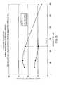
- FIG. 3is a graph of sheet resistance versus anneal time.
- FIG. 4is a graph of sheet resistance versus anneal temperature.
- FIG. 5is a flowchart of an embodiment of a method of fabricating a semiconductor device.
- FIG. 6is a cross-sectional view of an embodiment of a substrate used for fabrication of an embodiment of a MOSFET.
- FIGS. 7A and 7Bare cross-sectional views of structures at intermediate steps during fabrication of an embodiment of a MOSFET, utilizing the substrate of FIG. 6 .
- FIGS. 8A and 8Bare cross-sectional views of structures at fabrication steps that follow the steps illustrated in FIGS. 7A and 7B .
- MOSmetal-oxide-semiconductor
- the inventionprovides means to avoid separation of metal layer reaction with the substrate and metal layer reaction with a polycrystalline silicon portion of a gate contact.
- the inventionfurther provides improved gate design in conjunction with the advantages of a substrate that includes a SiGe layer, among other advantages.
- MOSis here used to refer generally to semiconductor devices that include a conductive gate spaced at least by an insulting layer from a semiconducting channel layer.
- SiGeand “Si 1-x Ge x ” are here used interchangeably to refer to silicon-germanium alloys.
- siicideis here used to refer to a reaction product of a metal, silicon, and optionally other components, such as germanium.
- siicideis also used, less formally, to refer to the reaction product of a metal with an elemental semiconductor, a compound semiconductor or an alloy semiconductor.
- FIG. 1is cross-sectional view of a conventional silicon-based MOS field-effect transistor (MOSFET) 100 .
- the transistor 100includes a gate contact 120 , a pair of spacers 150 , a source 135 , a source silicide contact 130 , a gate oxide 126 , a drain 145 , a drain silicide contact 140 and a silicon substrate 110 .
- the transistor 100is electrically isolated from neighboring transistors by a shallow trench isolation (STI) portion 170 .
- STIshallow trench isolation
- the gate contact 120includes a doped, conductive polycrystalline silicon (“polysilicon”) portion 124 proximal to the gate oxide 126 and a distal gate silicide portion 122 .
- the source 135 and drain 145include doped regions formed by implantation of dopant species into the substrate 110 and annealing, with the spacers 150 controlling the distribution of dopant beneath the gate oxide 126 .
- the silicide contacts 130 , 140 and gate silicide portion 122provide good ohmic interfaces respectively to the source 135 and drain 145 and to the gate polysilicon portion 124 .
- the MOSFET 100has a surface channel, which may be defined in physical or electrical terms. Physically, the surface channel is the p-type or n-type silicon that is adjacent to (i.e., below) the gate oxide 126 and which joins the source 135 and drain 145 . Electrically, the channel is an inversion layer, which provides current flow between the source 135 and drain 145 . Thus, from the electrical point of view, the presence and condition of the channel are variable.
- FIG. 2is a cross-sectional view of an embodiment of a MOSFET 200 , which is distinguished from the MOSFET 100 of FIG. 1 by the inclusion of a strained-silicon channel layer on a SiGe layer.
- the following description of the structure of the MOSFET 200is limited to features that are substantially different from features of the conventional MOSFET 100 .
- the MOSFET 200includes a strained-silicon layer 220 , a source 245 , a drain 255 , a source contact 240 , a drain contact 250 and a substrate 210 that includes a relaxed SiGe layer (other embodiments include a strained-SiGe layer).
- the silicon layer 220can be epitaxially grown on the substrate 210 , and provides a surface channel for the MOSFET 200 .
- the source and drain contacts 240 , 250can be formed by reacting a metal layer with portions of the substrate 210 and the silicon layer 220 .
- the source 245 and the drain 255can be formed by diffusing a dopant into the substrate 210 silicon layer 220 .
- the source and drain contacts 240 , 250can be formed by depositing a metal layer and reacting the metal layer with a portion of the substrate 210 , including, at least, portions of the silicon layer 220 and the relaxed SiGe layer.
- FIGS. 3 and 4silicidation of silicon and SiGe are compared.
- Conventional processing methodswould typically decouple the formation of the source and drain contacts 240 , 250 and the formation of the distal (upper) gate silicide portion 122 due to the differing silicidation behavior of SiGe in the substrate 210 and the polysilicon in the gate contact with a metal layer.
- the silicide formation rate of siliconcan be very different from the silicide formation rate of SiGe.
- FIGS. 3 and 4demonstrate differences in silicidation behavior between Si and SiGe after a single annealing step, it should be noted that silicidation processes can utilize multiple annealing steps, oftentimes with unreacted metal being stripped between anneals.
- FIG. 3is a graph showing two curves of the sheet resistance vs. anneal time for samples having a titanium metal layer on Si and on Si 0.7 Ge 0.3 during reaction at 675° C.
- Point Aindicates a typically desired interval of anneal time, between 100-150 seconds.
- the sheet resistance of the Si sampleis more twice that of the Si 0.7 Ge 0.3 sample.
- the sheet resistance of the Si sampleeventually drops below that of the Si 0.7 Ge 0.3 sample after more than 4 minutes of annealing.
- This time variable annealing behaviorarises from the differing reaction rates for silicide formation for Ti with Si and with SiGe.
- FIG. 4shows a graph of the sheet resistance vs. anneal temperature for samples of the same material combinations as those in FIG. 3 .
- the graphshows data taken at various time intervals, from 30 seconds to 5 minutes. Curves are shown for the sheet resistance vs. temperature after 2 minutes of reaction time.
- Point Bindicates a desirable anneal temperature of 675° C.
- the sheet resistance of the reacted Si sampleis more twice that of the reacted Si 0.7 Ge 0.3 sample for anneal times of approximately 2 minutes or less, again demonstrating the difference in the silicidation rates of Si and SiGe for desirable combinations of annealing time and temperature.
- One method for overcoming the differences in silicidation rates of gate and source-drain regionsis to decouple the gate silicide formation from the source-drain silicidation, as described in U.S. Pat. No. 4,755,478.
- the decoupled process for siliciding the source-drain regions and gate electrode regions of a SiGe substratetypically requires more processing steps due to separation of silicidation of polysilicon in a gate contact and silicidation of the source-drain contacts, each set of steps having different optimized conditions. Decoupling tends to increase the costs of the overall silicidation process.
- the silicidation of Sican occur at a much higher temperature than silicidation of SiGe. Therefore, an optimized silicidation process involving a polysilicon gate can make the SiGe substrate layer vulnerable to, for example, interdiffusion, dislocation redistribution and silicide agglomeration.
- Features of the inventioncan remove a need for decoupling, and provide gate contacts and source/drain contacts with similar, optimized processing conditions. The invention can further provide processing at lower temperatures.
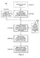
- FIG. 5is a flow diagram of an embodiment of a method 500 for fabricating a semiconductor device, according to principles of the invention. Fabrication can begin with provision of a silicon wafer (Step 510 ). A relaxed layer is provided (Step 520 ), and includes first and second materials, for example, silicon and germanium. For example, a substrate that includes a relaxed layer of SiGe, intermediate layers of SiGe and a silicon wafer can be provided; see, e.g., commonly assigned U.S. Pat. No. 6,107,653 to Fitzgerald.
- a channel layerfor example, of silicon, can be provided adjacent to the relaxed layer (Step 530 ).
- a surface channel silicon layercan be epitaxially grown on a SiGe relaxed layer.
- a buried channel layeris provided adjacent to the relaxed layer.
- Some of these embodimentsinclude one or more buried channel layers and a surface channel layer.
- the channel layerscan include, for example Si, Ge or SiGe.
- the composition of a channel layercan be chosen in cooperation with the composition of a relaxed layer to provide a desired level of strain in the channel layer, as is conventional in the art.
- the method 500further includes formation of a contact adjacent to the relaxed layer (Step 550 ).
- the contactincludes a portion that is proximal to the relaxed semiconductor layer and a portion that is distal to the relaxed semiconductor layer, i.e., lower and upper portions.
- the distal portionincludes the first material and the second material, and preferably has substantially the same composition as the relaxed semiconductor layer.
- Similar compositions, for example, of SiGe, in the relaxed layer and in the upper portion of the contactenable similar optimized processing conditions for reaction of a metal layer with the relaxed layer and with the upper portion of the contact. Thus, reaction of a metal layer can proceed simultaneously for the substrate and for the contact.
- Formation of the contactcan commence with formation of a lower portion that includes Si, Ge or SiGe (Step 540 ).
- the distal portioncan then be formed from SiGe having a different composition than the semiconductor of the proximal portion.
- the compositioncan vary abruptly or smoothly with position in the contact through the proximal and the distal portions.
- the composition of the proximal portioncan be chosen, for example, for its electrical performance or compatibility with an adjacent gate dielectric, as described in below.
- the composition of the distal portionin contrast, can be chosen to provide compatibility with the composition of the relaxed layer.
- the method 500further includes formation of a metal layer adjacent to the relaxed semiconductor layer and the distal portion of the contact (Step 560 ).
- the metalcan include, for example, titanium, cobalt, nickel, platinum, molybdenum, tungsten and/or zirconium.
- the metal layeris simultaneously reacted with the substrate and with the distal portion of the contact (Step 570 ).
- most of the metal layer that reacts with the substratewill react with the relaxed semiconductor layer, in part because any surface layers will be relatively thin. Thus, in these embodiments, the relaxed layer will dominate over other portions of the substrate in the reaction with the metal layer.
- the above-described methodpermits the formation of source and drain silicide contacts in a substrate at the same time as formation of a distal germanium silicide portion of a gate contact.
- Both gate silicide and source and drain silicidecan be formed under preferred time and temperature annealing conditions.
- the inventionfacilitates simultaneous processing.
- a substratethat includes a SiGe layer.
- the SiGe layercan be grown on a silicon wafer, and can include more than one layer of alloys of varying composition, thickness and growth conditions.
- the substratecan include a SiGe layer or multiple SiGe layers and/or SiGe layers having graded composition.
- the SiGe layerincludes a relaxed SiGe layer grown on intermediate SiGe layers that accommodate the lattice mismatch with a silicon wafer.
- the substratecan include, for example, a silicon wafer, with the SiGe layers grown on the silicon wafer.
- an oxide layercan be present between the silicon wafer and the SiGe layer.
- Other types of waferscan be used as a base for a substrate, e.g., silicon-on-insulator (SOI) wafers, germanium wafers, glass substrates and laminated substrates.
- SOIsilicon-on-insulator
- a channel layercan be a surface or a buried layer, and can be formed, for example, from silicon, germanium or a combination of silicon and germanium.
- a buried channel layercan be a strained silicon layer epitaxially grown on a relaxed SiGe layer.
- the buried layercan be germanium or can be SiGe having a composition that is different from the SiGe of the relaxed layer.
- the buried channel layercan have a composition of Si 1-x Ge x while the relaxed layer has a composition of Si 1-y Ge y .
- the buried SiGe layeris under compressive stress, and thus exhibits a compressive strain.
- material combinationscan be chosen to provide a p-channel MOSFET, preferably by providing a compressively strained SiGe buried layer, or an n-channel MOSFET, preferable by providing a tensilely strained silicon layer.
- Some preferred embodiments of the inventionuse relaxed SiGe layers grown on silicon substrates. Silicon, germanium and SiGe layers can be grown via known epitaxial growth techniques. Growth of a buried layer of silicon, germanium or SiGe on a SiGe relaxed layer, or SiGe on silicon, enables production of buried layers of controlled stress and dislocation density.
- Examples of SiGe substrates, in which the Ge content can be up to 100%,include: a relaxed, uniform composition SiGe layer on a graded composition SiGe layer atop a Si substrate; a relaxed, uniform composition SiGe layer directly adjacent to a Si substrate; and a relaxed, uniform composition SiGe layer on an insulating layer like SiO 2 , adjacent a Si substrate.
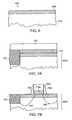
- FIGS. 6-8are chronologically arranged cross-sectional views of MOSFET-related structures at various stages of an embodiment of a MOSFET fabrication process.
- the completed embodiment of a MOSFET 900is shown in FIG. 8B .
- FIG. 6illustrates an embodiment of a substrate 600 used as a base for fabrication of the embodiment of the MOSFET 900 .
- the substrate 600includes a relaxed SiGe layer 610 and a strained Si surface layer 640 .
- the substrate 600can provide a base for the fabrication of semiconductor devices, such as transistors.
- the substrate 600can be manufactured via epitaxial growth and polishing techniques, as described in commonly assigned U.S. Pat. No. 6,107,653 to Fitzgerald.
- the relaxed SiGe substrate layer 610can form the base substrate of many types of MOSFET devices.
- the thin strained Si layer 640can alternatively be a SiGe layer, a sequence of Si and SiGe layers, or other combination of thin epitaxial layers, as described above.
- FIGS. 7 A-Billustrate some fabrication steps of a gate contact for the MOSFET 900 .
- FIG. 7Ashows a cross-sectional view of a device at a stage of fabrication, chronologically following the stage of FIG. 6 .
- regions of isolation portions 730have been formed in the substrate 600 to provide a modified substrate 600 a .
- a dielectric layer 710 and a polycrystalline semiconductor layer 720have been formed on the substrate 600 a .
- the polycrystalline semiconductor layer 720can include silicon and germanium.
- the isolation portion 730preferably is deep enough to cross all channel layers of semiconductor material in the substrate 600 a , ending at least in the SiGe relaxed layer of the substrate 600 a .
- the isolation portions 730are absent or replaced by other isolation means.
- one embodimentincludes semi-recessed oxide isolation (S-ROX) portions.
- S-ROXsemi-recessed oxide isolation
- a relatively high degree of planarityis preferably maintained between the upper surface of the substrate 600 a and the upper surface of the isolation portions 730 .
- the dielectric layer 710which provides a gate dielectric, is formed on the exposed surface of the substrate 600 , possibly consuming a portion of the surface of the strained-silicon layer 640 .
- the dielectric layer 710can be formed by various methods conventional in the art, e.g., via thermal oxidation of the surface of the substrate 600 or via a deposition technique.
- the dielectric layer 710can be, for example, a 15-100 ⁇ (1.5-10.0 nm) thick layer of silicon dioxide.
- Other embodimentsinclude other suitable dielectric materials, e.g., silicon oxynitride, silicon nitride, a plurality of silicon nitride and silicon oxide layers, or a high-k dielectric.
- a polycrystalline semiconductor layer 720is then deposited on the dielectric layer 710 , e.g., via chemical-vapor deposition.
- the polycrystalline semiconductor layer 720can be, for example, 1000 ⁇ (100 nm) thick.
- the polycrystalline semiconductor layer 720preferably has an upper portion including SiGe with a Ge content substantially identical to the Ge content of the relaxed SiGe layer 610 .
- a proximal (lower) portion of the layer 720has a different composition from that of the distal (upper) portion of the layer 720 .
- the composition of the distal portioncan be matched to the substrate layer 610 , while the portion in contact with the dielectric layer 710 can have a composition chosen, for example, for its compatibility with the dielectric material.
- polycrystalline siliconis highly compatible with silicon dioxide dielectric, the interface between these two materials has a relatively very low electrical defect density.
- FIG. 7Billustrates another stage in the production of the MOSFET 900 , related to some steps in the formation of a gate contact.
- the dielectric layer 710 and the polycrystalline semiconductor layer 720have been patterned to respectively form a gate dielectric 710 a and a gate contact semiconductor portion 720 a .
- the patterningcan be performed via methods conventional in the art, e.g., via photolithography and sputter etching.
- Contact sidewall spacers 740have been formed prior to formation of a source region 750 , and a drain region 760 .
- the sidewall spacers 740can provide isolation between the gate contact and source/drain regions 750 , 760 , and facilitate fabrication of self-aligned structures.
- the spacers 740can be formed via methods conventional in the art, e.g., via oxide deposition, thermal oxidation of polysilicon and/or nitride deposition.
- the source region 750 and the drain region 760include dopant, which extends across the interface between the silicon surface layer 640 and the SiGe relaxed layer in the further modified substrate 600 b.
- the structures illustrated in FIG. 7Bare fabricated as follows.
- a layer of photosensitive polymere.g., a Novolak-based photoresist, as known to one having ordinary skill in the semiconductor lithography arts
- the polymeris exposed and developed to define a photo-mask having substantially vertical sidewalls.
- the exposed portions of SiGe semiconductor layer 720are sequentially etched in a directional mode to define the gate contact semiconductor portion 720 a .
- the photo-maskis removed, e.g., via an O 2 plasma etch.
- the sidewall spacers 740are formed on the exposed sides of the gate contact semiconductor portion 720 a .
- the sidewall spacers 740can be formed using one of several known methods.
- a preferred methodis to deposit a layer of chemically vapor-deposited (CVD) oxide over the entire structure, and directionally etch the deposited layer so that it is removed from the horizontal surfaces of the substrate. During this removal step, exposed portions of the underlying dielectric layer 710 are also removed to define the gate dielectric 710 a.
- CVDchemically vapor-deposited
- the source region 750 and the drain region 760are defined, for example, through ion implantation and drive-in anneal.
- the diffusion regionscan be formed using one of several techniques. For example, implantation of dopant ions to define the diffusion regions can use the gate contact and isolation regions 730 as an implantation mask.
- FIG. 8A -Billustrate aspects of silicide formation for the MOSFET 900 .
- FIG. 8Aillustrates deposition of a metal layer 820 on the structures illustrated in FIG. 7B .
- the metal layer 820is formed during a single deposition step, and is adjacent to portions of both the substrate 600 b and the gate contact semiconductor portion 720 a .
- the metal layer 820preferably is approximately 8-20 nanometers (nm) in thickness.
- FIG. 8Bis a cross-sectional view of the completed embodiment of the MOSFET 900 .
- the MOSFET 900includes a gate contact silicide 920 , source contact silicide 950 and a drain contact silicide 960 .
- the gate contact silicide 920forms from reaction of a portion of the metal layer 820 with SiGe in the gate contact semiconductor portion 720 a .
- the source and drain contacts 950 , 960form from reaction of a portion of the metal layer 820 with Si and SiGe in the substrate 600 b , thus leaving a further modified substrate 600 c .
- the metal layer 820reacts with SiGe having similar or identical compositions in both the gate contact and in the substrate 600 b , providing common silicidation behavior and silicide formation in a single step.
- an unreacted gate semiconductor portion 720 bcan remain in the contact.
- the gate contact semiconductor portion 720 aincludes SiGe with a graded composition.
- a distal portion of the gate contact semiconductor portion 720 ahas a composition that matches the relaxed SiGe layer 610 , and a proximal portion, adjacent to the gate dielectric 710 a , that has a greater Ge content.
- the greater Ge contentcan be substantially pure Ge.
- a proximal portion of the gate contact semiconductor portion 720 ais substantially pure silicon.
- This embodimentprovides single-step silicidation of source, drain and gate, as well as a high quality gate contact/gate oxide interface, for example when the gate oxide 710 a is a silicon dioxide. It can also provide, for example, a gate contact work function that is similar/identical to conventional MOSFETS.
Landscapes
- Engineering & Computer Science (AREA)
- Microelectronics & Electronic Packaging (AREA)
- Condensed Matter Physics & Semiconductors (AREA)
- General Physics & Mathematics (AREA)
- Manufacturing & Machinery (AREA)
- Computer Hardware Design (AREA)
- Physics & Mathematics (AREA)
- Power Engineering (AREA)
- Chemical & Material Sciences (AREA)
- Chemical Kinetics & Catalysis (AREA)
- Insulated Gate Type Field-Effect Transistor (AREA)
- Crystallography & Structural Chemistry (AREA)
- Electrodes Of Semiconductors (AREA)
Abstract
Description
- The invention generally relates to semiconductor devices, and, more particularly, to the fabrication and structure of contacts in transistors.
- Continuous improvements in the fabrication and design of semiconductor transistors used in integrated circuit devices have permitted ever greater area densities of transistors. Development of materials and processing for interconnects and contacts plays a large role in transistor development.
- Materials and processes for forming conductive contacts and interconnects must accommodate, for example, dimensional requirements, processing temperatures, reliability needs and materials compatibility. Traditional aluminum-based interconnects have gradually given way to copper interconnects for fine dimensions; cobalt silicide and other metallic materials are gradually supplanting titanium silicide source and drain contacts and titanium silicide caps on doped polycrystalline silicon gate contacts.
- Another avenue for improvement in device performance involves the use of newer types of substrates as replacements for traditional silicon wafers. For example, wafers that have a silicon-germanium (SiGe) layer can provide improved channel layer performance in a strained-silicon layer grown on the SiGe layer.
- Mobility enhancements obtained from strained silicon, in combination with source-drain and gate silicidation techniques, provide the opportunity to increase speed, reduce power consumption, and provide the basis of other advances in microelectronics, such as analog and digital device integration.
- The use of substrates that include a SiGe layer, however, can increase fabrication complexity relative to that for conventional silicon wafer-based devices. For example, formation of source and drain contacts through reaction of a metal layer, such as titanium or cobalt, with SiGe in the substrate has preferred process conditions that are different from silicide formation with relatively pure silicon.
- The invention involves structures and fabrication methods for semiconductor devices that preferably have semiconductor layers including two materials in both a substrate and in a gate contact. The invention provides simplified processing for semiconductor devices, as well as improved semiconductor device structures that include compound and/or alloyed semiconductors in both contacts and substrates. The invention provides for simultaneous reaction of a metal layer to form reacted material contacts in the substrate and a reacted material upper portion of a gate contact. The metal layer exhibits a similar reaction behavior with the semiconductor layers in both the substrate and in the upper portion of the gate contact due to a similar composition ratio of the two materials in both semiconductor layers.
- Preferred embodiments of the invention feature substrates and contacts that include one or more semiconductor alloy layers of silicon and germanium. Preferred embodiments include SiGe layers of similar composition in both a substrate and a contact; conductive portions are formed by simultaneously reacting the SiGe layers in the substrate and the contact with a metal layer. Thus, for example, source and drain contacts in a substrate can be formed simultaneously with formation of a conductive upper (distal) portion of a gate contact having a portion that includes the semiconductor alloy. In this way, some processing steps are rendered unnecessary during basic device fabrication.
- Simplified processing can be achieved in part because reaction of a metal layer with the substrate and with a semiconductor layer in a gate contact need not be decoupled to accommodate, for example, SiGe in the substrate and polycrystalline silicon in the gate. Proper material selection provides substrates and gate contacts that have similar or identical silicide formation steps. Other benefits can arise, such as lower temperature processing for silicide formation.
- In preferred embodiments, the invention features transistors that include a gate electrode including SiGe in at least an upper portion of a gate contact (i.e., electrode) and a strained-silicon channel layer on a relaxed SiGe layer in a substrate. By having SiGe in an upper portion of a gate electrode, the silicidation of gate and source-drain regions can be performed in a single process. A lower portion of the gate contact can have a different material composition, chosen to provide, for example, a desired electrical property and/or compatibility with a gate dielectric material.
- Thus, in a first aspect, the invention features a method for fabricating a semiconductor device. The method includes provision of a semiconductor layer that includes a first material and a second material. The semiconductor layer can be an alloy of two or more materials. The first and second materials can be silicon and germanium.
- The semiconductor layer can be or include a relaxed layer. The relaxed layer can be part of a substrate having a portion, adjacent to the relaxed layer, with a lattice spacing mismatched to that of the relaxed layer. For example, the relaxed layer can be grown on intermediate layers that accommodate mismatch to a silicon wafer. As another example, the relaxed layer can reside on an oxide layer.
- The method also includes the formation of a contact that has a portion proximal to the relaxed semiconductor layer and a portion distal to the relaxed semiconductor layer. The distal portion includes the first material and the second material. A metal layer is formed adjacent to the relaxed semiconductor layer and adjacent to the distal portion of the contact. The metal layer is simultaneously reacted with the relaxed semiconductor layer and with the distal portion of the contact.
- The silicon and germanium of the distal portion of the contact can have an atomic density ratio that is substantially the same as an atomic density ratio of the silicon and germanium of the relaxed semiconductor layer. The proximal portion of the contact can consist essentially of silicon or essentially of germanium. Alternatively the proximal portion can include silicon and germanium; the atomic density ratio of the silicon and germanium of the proximal portion can differ from the atomic density ratio of the silicon and germanium of the distal portion.
- In a second aspect, the invention features a semiconductor device. The device includes a substrate that has a reacted conductive layer that comprises silicon, germanium and a metallic material. The metallic material can be, e.g., titanium, nickel or cobalt. The device also includes a contact that has a portion proximal to the substrate and a reacted conductive portion distal to the substrate. The reacted conductive distal portion of the contact includes silicon, germanium and the same metallic material as in the substrate reacted conductive layer. The substrate can further include a strained semiconductor layer, for example, of silicon, adjacent to the contact.
- In a third aspect, the invention features a semiconductor device that includes a substrate that has a reacted conductive layer comprising a first material, a second material and a metallic material. The device includes a contact having a portion proximal to the substrate and a reacted conductive portion distal to the substrate, the distal portion comprising the first material, the second material and the metallic material.
- In the drawings, like reference characters generally refer to the same parts throughout the different views. Also, the drawings are not necessarily to scale, emphasis instead generally being placed upon illustrating the principles of the invention.
FIG. 1 is a cross-sectional view of a conventional silicon-based MOSFET.FIG. 2 is a cross-sectional view of an embodiment of a MOSFET that includes a strained-silicon channel layer on a SiGe layer.FIG. 3 is a graph of sheet resistance versus anneal time.FIG. 4 is a graph of sheet resistance versus anneal temperature.FIG. 5 is a flowchart of an embodiment of a method of fabricating a semiconductor device.FIG. 6 is a cross-sectional view of an embodiment of a substrate used for fabrication of an embodiment of a MOSFET.FIGS. 7A and 7B are cross-sectional views of structures at intermediate steps during fabrication of an embodiment of a MOSFET, utilizing the substrate ofFIG. 6 .FIGS. 8A and 8B are cross-sectional views of structures at fabrication steps that follow the steps illustrated inFIGS. 7A and 7B .- Various features of the invention are well suited to application in metal-oxide-semiconductor (MOS) transistors having Si, Si1-xGexand/or Ge layers in and or on a substrate. The invention provides means to avoid separation of metal layer reaction with the substrate and metal layer reaction with a polycrystalline silicon portion of a gate contact. The invention further provides improved gate design in conjunction with the advantages of a substrate that includes a SiGe layer, among other advantages.
- The term “MOS” is here used to refer generally to semiconductor devices that include a conductive gate spaced at least by an insulting layer from a semiconducting channel layer. The terms “SiGe” and “Si1-xGex” are here used interchangeably to refer to silicon-germanium alloys. The term “silicide” is here used to refer to a reaction product of a metal, silicon, and optionally other components, such as germanium. The term “silicide” is also used, less formally, to refer to the reaction product of a metal with an elemental semiconductor, a compound semiconductor or an alloy semiconductor.
- First, with reference to
FIG. 1 , to provide a context for description of features of the invention, the structure and operation of a conventional MOSFET are described.FIG. 1 is cross-sectional view of a conventional silicon-based MOS field-effect transistor (MOSFET)100. Thetransistor 100 includes agate contact 120, a pair ofspacers 150, asource 135, asource silicide contact 130, agate oxide 126, adrain 145, adrain silicide contact 140 and asilicon substrate 110. Thetransistor 100 is electrically isolated from neighboring transistors by a shallow trench isolation (STI)portion 170. - The
gate contact 120 includes a doped, conductive polycrystalline silicon (“polysilicon”)portion 124 proximal to thegate oxide 126 and a distalgate silicide portion 122. Thesource 135 and drain145 include doped regions formed by implantation of dopant species into thesubstrate 110 and annealing, with thespacers 150 controlling the distribution of dopant beneath thegate oxide 126. Thesilicide contacts gate silicide portion 122 provide good ohmic interfaces respectively to thesource 135 and drain145 and to thegate polysilicon portion 124. - The
MOSFET 100 has a surface channel, which may be defined in physical or electrical terms. Physically, the surface channel is the p-type or n-type silicon that is adjacent to (i.e., below) thegate oxide 126 and which joins thesource 135 and drain145. Electrically, the channel is an inversion layer, which provides current flow between thesource 135 and drain145. Thus, from the electrical point of view, the presence and condition of the channel are variable. FIG. 2 is a cross-sectional view of an embodiment of aMOSFET 200, which is distinguished from theMOSFET 100 ofFIG. 1 by the inclusion of a strained-silicon channel layer on a SiGe layer. The following description of the structure of theMOSFET 200 is limited to features that are substantially different from features of theconventional MOSFET 100.- The
MOSFET 200 includes a strained-silicon layer 220, asource 245, adrain 255, asource contact 240, adrain contact 250 and asubstrate 210 that includes a relaxed SiGe layer (other embodiments include a strained-SiGe layer). Thesilicon layer 220 can be epitaxially grown on thesubstrate 210, and provides a surface channel for theMOSFET 200. The source anddrain contacts substrate 210 and thesilicon layer 220. Thesource 245 and thedrain 255 can be formed by diffusing a dopant into thesubstrate 210silicon layer 220. The source anddrain contacts substrate 210, including, at least, portions of thesilicon layer 220 and the relaxed SiGe layer. - Referring now to
FIGS. 3 and 4 , silicidation of silicon and SiGe are compared. Conventional processing methods would typically decouple the formation of the source anddrain contacts gate silicide portion 122 due to the differing silicidation behavior of SiGe in thesubstrate 210 and the polysilicon in the gate contact with a metal layer. As described below, with reference toFIGS. 3 and 4 , the silicide formation rate of silicon can be very different from the silicide formation rate of SiGe. WhileFIGS. 3 and 4 demonstrate differences in silicidation behavior between Si and SiGe after a single annealing step, it should be noted that silicidation processes can utilize multiple annealing steps, oftentimes with unreacted metal being stripped between anneals. FIG. 3 is a graph showing two curves of the sheet resistance vs. anneal time for samples having a titanium metal layer on Si and on Si0.7Ge0.3during reaction at 675° C. Point A indicates a typically desired interval of anneal time, between 100-150 seconds. At this time, the sheet resistance of the Si sample is more twice that of the Si0.7Ge0.3sample. The sheet resistance of the Si sample eventually drops below that of the Si0.7Ge0.3sample after more than 4 minutes of annealing. This time variable annealing behavior arises from the differing reaction rates for silicide formation for Ti with Si and with SiGe.FIG. 4 shows a graph of the sheet resistance vs. anneal temperature for samples of the same material combinations as those inFIG. 3 . The graph shows data taken at various time intervals, from 30 seconds to 5 minutes. Curves are shown for the sheet resistance vs. temperature after 2 minutes of reaction time.- Point B indicates a desirable anneal temperature of 675° C. The sheet resistance of the reacted Si sample is more twice that of the reacted Si0.7Ge0.3sample for anneal times of approximately 2 minutes or less, again demonstrating the difference in the silicidation rates of Si and SiGe for desirable combinations of annealing time and temperature.
- One method for overcoming the differences in silicidation rates of gate and source-drain regions is to decouple the gate silicide formation from the source-drain silicidation, as described in U.S. Pat. No. 4,755,478. The decoupled process for siliciding the source-drain regions and gate electrode regions of a SiGe substrate typically requires more processing steps due to separation of silicidation of polysilicon in a gate contact and silicidation of the source-drain contacts, each set of steps having different optimized conditions. Decoupling tends to increase the costs of the overall silicidation process.
- The silicidation of Si can occur at a much higher temperature than silicidation of SiGe. Therefore, an optimized silicidation process involving a polysilicon gate can make the SiGe substrate layer vulnerable to, for example, interdiffusion, dislocation redistribution and silicide agglomeration. Features of the invention can remove a need for decoupling, and provide gate contacts and source/drain contacts with similar, optimized processing conditions. The invention can further provide processing at lower temperatures.
FIG. 5 is a flow diagram of an embodiment of amethod 500 for fabricating a semiconductor device, according to principles of the invention. Fabrication can begin with provision of a silicon wafer (Step510). A relaxed layer is provided (Step520), and includes first and second materials, for example, silicon and germanium. For example, a substrate that includes a relaxed layer of SiGe, intermediate layers of SiGe and a silicon wafer can be provided; see, e.g., commonly assigned U.S. Pat. No. 6,107,653 to Fitzgerald.- A channel layer, for example, of silicon, can be provided adjacent to the relaxed layer (Step530). For example, a surface channel silicon layer can be epitaxially grown on a SiGe relaxed layer. In some embodiments, a buried channel layer is provided adjacent to the relaxed layer. Some of these embodiments include one or more buried channel layers and a surface channel layer. The channel layers can include, for example Si, Ge or SiGe. The composition of a channel layer can be chosen in cooperation with the composition of a relaxed layer to provide a desired level of strain in the channel layer, as is conventional in the art.
- The
method 500 further includes formation of a contact adjacent to the relaxed layer (Step550). The contact includes a portion that is proximal to the relaxed semiconductor layer and a portion that is distal to the relaxed semiconductor layer, i.e., lower and upper portions. The distal portion includes the first material and the second material, and preferably has substantially the same composition as the relaxed semiconductor layer. Similar compositions, for example, of SiGe, in the relaxed layer and in the upper portion of the contact enable similar optimized processing conditions for reaction of a metal layer with the relaxed layer and with the upper portion of the contact. Thus, reaction of a metal layer can proceed simultaneously for the substrate and for the contact. - Formation of the contact can commence with formation of a lower portion that includes Si, Ge or SiGe (Step540). The distal portion can then be formed from SiGe having a different composition than the semiconductor of the proximal portion. The composition can vary abruptly or smoothly with position in the contact through the proximal and the distal portions. Thus, the composition of the proximal portion can be chosen, for example, for its electrical performance or compatibility with an adjacent gate dielectric, as described in below. The composition of the distal portion, in contrast, can be chosen to provide compatibility with the composition of the relaxed layer.
- The
method 500 further includes formation of a metal layer adjacent to the relaxed semiconductor layer and the distal portion of the contact (Step560). The metal can include, for example, titanium, cobalt, nickel, platinum, molybdenum, tungsten and/or zirconium. The metal layer is simultaneously reacted with the substrate and with the distal portion of the contact (Step570). In preferred embodiments, most of the metal layer that reacts with the substrate will react with the relaxed semiconductor layer, in part because any surface layers will be relatively thin. Thus, in these embodiments, the relaxed layer will dominate over other portions of the substrate in the reaction with the metal layer. - In the case of a substrate that includes a SiGe relaxed semiconductor layer, the above-described method permits the formation of source and drain silicide contacts in a substrate at the same time as formation of a distal germanium silicide portion of a gate contact. Both gate silicide and source and drain silicide can be formed under preferred time and temperature annealing conditions. Thus, rather than decoupling the formation of a conductive cap for the gate contact and formation of source and drain contacts, the invention facilitates simultaneous processing.
- Various preferred embodiments of the invention utilize a substrate that includes a SiGe layer. The SiGe layer can be grown on a silicon wafer, and can include more than one layer of alloys of varying composition, thickness and growth conditions. Thus, the substrate can include a SiGe layer or multiple SiGe layers and/or SiGe layers having graded composition. In some embodiments, the SiGe layer includes a relaxed SiGe layer grown on intermediate SiGe layers that accommodate the lattice mismatch with a silicon wafer.
- The substrate can include, for example, a silicon wafer, with the SiGe layers grown on the silicon wafer. In this case, an oxide layer can be present between the silicon wafer and the SiGe layer. Other types of wafers can be used as a base for a substrate, e.g., silicon-on-insulator (SOI) wafers, germanium wafers, glass substrates and laminated substrates.
- A channel layer can be a surface or a buried layer, and can be formed, for example, from silicon, germanium or a combination of silicon and germanium. For example, a buried channel layer can be a strained silicon layer epitaxially grown on a relaxed SiGe layer. Alternatively, the buried layer, can be germanium or can be SiGe having a composition that is different from the SiGe of the relaxed layer.
- For example, the buried channel layer can have a composition of Si1-xGexwhile the relaxed layer has a composition of Si1-yGey. For x>y, the buried SiGe layer is under compressive stress, and thus exhibits a compressive strain. Thus, material combinations can be chosen to provide a p-channel MOSFET, preferably by providing a compressively strained SiGe buried layer, or an n-channel MOSFET, preferable by providing a tensilely strained silicon layer.
- Some preferred embodiments of the invention use relaxed SiGe layers grown on silicon substrates. Silicon, germanium and SiGe layers can be grown via known epitaxial growth techniques. Growth of a buried layer of silicon, germanium or SiGe on a SiGe relaxed layer, or SiGe on silicon, enables production of buried layers of controlled stress and dislocation density. Examples of SiGe substrates, in which the Ge content can be up to 100%, include: a relaxed, uniform composition SiGe layer on a graded composition SiGe layer atop a Si substrate; a relaxed, uniform composition SiGe layer directly adjacent to a Si substrate; and a relaxed, uniform composition SiGe layer on an insulating layer like SiO2, adjacent a Si substrate.
- Referring now to
FIGS. 6-8 , steps in an embodiment of a MOSFET fabrication process, and some preferred device structures, are described.FIGS. 6-8 are chronologically arranged cross-sectional views of MOSFET-related structures at various stages of an embodiment of a MOSFET fabrication process. The completed embodiment of aMOSFET 900 is shown inFIG. 8B . FIG. 6 illustrates an embodiment of asubstrate 600 used as a base for fabrication of the embodiment of theMOSFET 900. Thesubstrate 600 includes arelaxed SiGe layer 610 and a strainedSi surface layer 640. Thesubstrate 600 can provide a base for the fabrication of semiconductor devices, such as transistors. Thesubstrate 600 can be manufactured via epitaxial growth and polishing techniques, as described in commonly assigned U.S. Pat. No. 6,107,653 to Fitzgerald.- It will be appreciated by those skilled in the art that the relaxed
SiGe substrate layer 610 can form the base substrate of many types of MOSFET devices. The thinstrained Si layer 640 can alternatively be a SiGe layer, a sequence of Si and SiGe layers, or other combination of thin epitaxial layers, as described above. - FIGS.7A-B illustrate some fabrication steps of a gate contact for the
MOSFET 900.FIG. 7A shows a cross-sectional view of a device at a stage of fabrication, chronologically following the stage ofFIG. 6 . At this stage, regions ofisolation portions 730 have been formed in thesubstrate 600 to provide a modifiedsubstrate 600a. Adielectric layer 710 and apolycrystalline semiconductor layer 720 have been formed on thesubstrate 600a. Thepolycrystalline semiconductor layer 720 can include silicon and germanium. - The
isolation portion 730 preferably is deep enough to cross all channel layers of semiconductor material in thesubstrate 600a, ending at least in the SiGe relaxed layer of thesubstrate 600a. In other embodiments, theisolation portions 730 are absent or replaced by other isolation means. For example, one embodiment includes semi-recessed oxide isolation (S-ROX) portions. Generally, a relatively high degree of planarity is preferably maintained between the upper surface of thesubstrate 600aand the upper surface of theisolation portions 730. - The
dielectric layer 710, which provides a gate dielectric, is formed on the exposed surface of thesubstrate 600, possibly consuming a portion of the surface of the strained-silicon layer 640. Thedielectric layer 710 can be formed by various methods conventional in the art, e.g., via thermal oxidation of the surface of thesubstrate 600 or via a deposition technique. - The
dielectric layer 710 can be, for example, a 15-100 Å (1.5-10.0 nm) thick layer of silicon dioxide. Other embodiments include other suitable dielectric materials, e.g., silicon oxynitride, silicon nitride, a plurality of silicon nitride and silicon oxide layers, or a high-k dielectric. - A
polycrystalline semiconductor layer 720 is then deposited on thedielectric layer 710, e.g., via chemical-vapor deposition. Thepolycrystalline semiconductor layer 720 can be, for example, 1000 Å (100 nm) thick. - The
polycrystalline semiconductor layer 720 preferably has an upper portion including SiGe with a Ge content substantially identical to the Ge content of therelaxed SiGe layer 610. In some embodiments, a proximal (lower) portion of thelayer 720 has a different composition from that of the distal (upper) portion of thelayer 720. Thus, the composition of the distal portion can be matched to thesubstrate layer 610, while the portion in contact with thedielectric layer 710 can have a composition chosen, for example, for its compatibility with the dielectric material. For example, polycrystalline silicon is highly compatible with silicon dioxide dielectric, the interface between these two materials has a relatively very low electrical defect density. FIG. 7B illustrates another stage in the production of theMOSFET 900, related to some steps in the formation of a gate contact. Thedielectric layer 710 and thepolycrystalline semiconductor layer 720 have been patterned to respectively form a gate dielectric710aand a gatecontact semiconductor portion 720a. The patterning can be performed via methods conventional in the art, e.g., via photolithography and sputter etching.- Contact
sidewall spacers 740 have been formed prior to formation of asource region 750, and adrain region 760. The sidewall spacers740 can provide isolation between the gate contact and source/drain regions spacers 740 can be formed via methods conventional in the art, e.g., via oxide deposition, thermal oxidation of polysilicon and/or nitride deposition. - The
source region 750 and thedrain region 760 include dopant, which extends across the interface between thesilicon surface layer 640 and the SiGe relaxed layer in the further modifiedsubstrate 600b. - For one embodiment of the
MOSFET 900, the structures illustrated inFIG. 7B are fabricated as follows. A layer of photosensitive polymer (e.g., a Novolak-based photoresist, as known to one having ordinary skill in the semiconductor lithography arts) is coated on a polycrystalline-SiGe semiconductor layer 720. The polymer is exposed and developed to define a photo-mask having substantially vertical sidewalls. The exposed portions ofSiGe semiconductor layer 720 are sequentially etched in a directional mode to define the gatecontact semiconductor portion 720a. The photo-mask is removed, e.g., via an O2plasma etch. - The sidewall spacers740 are formed on the exposed sides of the gate
contact semiconductor portion 720a. The sidewall spacers740 can be formed using one of several known methods. A preferred method is to deposit a layer of chemically vapor-deposited (CVD) oxide over the entire structure, and directionally etch the deposited layer so that it is removed from the horizontal surfaces of the substrate. During this removal step, exposed portions of theunderlying dielectric layer 710 are also removed to define the gate dielectric710a. - After the
sidewall spacers 740 are formed, thesource region 750 and thedrain region 760 are defined, for example, through ion implantation and drive-in anneal. The diffusion regions can be formed using one of several techniques. For example, implantation of dopant ions to define the diffusion regions can use the gate contact andisolation regions 730 as an implantation mask. FIG. 8A -B illustrate aspects of silicide formation for theMOSFET 900.FIG. 8A illustrates deposition of ametal layer 820 on the structures illustrated inFIG. 7B . Themetal layer 820 is formed during a single deposition step, and is adjacent to portions of both thesubstrate 600band the gatecontact semiconductor portion 720a. Themetal layer 820 preferably is approximately 8-20 nanometers (nm) in thickness.FIG. 8B is a cross-sectional view of the completed embodiment of theMOSFET 900. Upon annealing of the structures shown inFIG. 8A , and removal of residual portions of themetal layer 820, self-aligned gate and source-drain silicide contacts are formed, as described below; theMOSFET 900 includes agate contact silicide 920,source contact silicide 950 and adrain contact silicide 960.- The
gate contact silicide 920, forms from reaction of a portion of themetal layer 820 with SiGe in the gatecontact semiconductor portion 720a. The source anddrain contacts metal layer 820 with Si and SiGe in thesubstrate 600b, thus leaving a further modifiedsubstrate 600c. Themetal layer 820 reacts with SiGe having similar or identical compositions in both the gate contact and in thesubstrate 600b, providing common silicidation behavior and silicide formation in a single step. - After reaction of the
metal layer 820 with neighboring material, an unreactedgate semiconductor portion 720bcan remain in the contact. Some metals that can be used in themetal layer 820 are described in the following: - Titanium—can provide a good silicide on SiGe, but generally not well suited to short gate length polysilicon gates.
- Cobalt—generally preferable relative to Ti for sub-quarter micrometer linewidths, but can lead to agglomeration problems in conjunction with SiGe having a Ge atomic fraction of greater than approximately 15%.
- Nickel—generally works well with SiGe, at least for Ge atomic compositions of up to 45-50% or more, and consumes less silicon during silicidation than some other metals.
- Platinum—generally works well with SiGe, at least for Ge atomic compositions of up to 45-50% or more.
- Zirconium—can be used with SiGe.
- Multilayered metals—stacked metal layers (e.g., Pt/Ni) can be used.
- Alloys—can be used (e.g., NiPt).
- In one embodiment of the
MOSFET 900, the gatecontact semiconductor portion 720aincludes SiGe with a graded composition. In this embodiment, a distal portion of the gatecontact semiconductor portion 720ahas a composition that matches therelaxed SiGe layer 610, and a proximal portion, adjacent to the gate dielectric710a, that has a greater Ge content. The greater Ge content can be substantially pure Ge. This embodiment provides single-step silicidation of source, drain and gate with the further advantage of an improved work function due to the elevated Ge content at the interface with the gate dielectric710a. - In another embodiment, a proximal portion of the gate
contact semiconductor portion 720ais substantially pure silicon. This embodiment provides single-step silicidation of source, drain and gate, as well as a high quality gate contact/gate oxide interface, for example when thegate oxide 710ais a silicon dioxide. It can also provide, for example, a gate contact work function that is similar/identical to conventional MOSFETS. - Variations, modifications, and other implementations of what is described herein will occur to those of ordinary skill in the art without departing from the spirit and the scope of the invention as claimed. Accordingly, the invention is to be defined not by the preceding illustrative description but instead by the spirit and scope of the following claims.
Claims (33)
Priority Applications (6)
| Application Number | Priority Date | Filing Date | Title |
|---|---|---|---|
| US10/944,618US8129821B2 (en) | 2002-06-25 | 2004-09-17 | Reacted conductive gate electrodes |
| US13/342,589US8785315B2 (en) | 2002-06-25 | 2012-01-03 | Reacted conductive gate electrodes and methods of making the same |
| US14/320,065US9048167B2 (en) | 2002-06-25 | 2014-06-30 | Reacted conductive gate electrodes and methods of making the same |
| US14/697,337US9343539B2 (en) | 2002-06-25 | 2015-04-27 | Reacted conductive gate electrodes and methods of making the same |
| US15/137,517US9812572B2 (en) | 2002-06-25 | 2016-04-25 | Reacted conductive gate electrodes and methods of making the same |
| US15/784,925US10629735B2 (en) | 2002-06-25 | 2017-10-16 | Reacted conductive gate electrodes and methods of making the same |
Applications Claiming Priority (2)
| Application Number | Priority Date | Filing Date | Title |
|---|---|---|---|
| US10/179,079US6982474B2 (en) | 2002-06-25 | 2002-06-25 | Reacted conductive gate electrodes |
| US10/944,618US8129821B2 (en) | 2002-06-25 | 2004-09-17 | Reacted conductive gate electrodes |
Related Parent Applications (1)
| Application Number | Title | Priority Date | Filing Date |
|---|---|---|---|
| US10/179,079ContinuationUS6982474B2 (en) | 2002-06-25 | 2002-06-25 | Reacted conductive gate electrodes |
Related Child Applications (1)
| Application Number | Title | Priority Date | Filing Date |
|---|---|---|---|
| US13/342,589ContinuationUS8785315B2 (en) | 2002-06-25 | 2012-01-03 | Reacted conductive gate electrodes and methods of making the same |
Publications (2)
| Publication Number | Publication Date |
|---|---|
| US20050042849A1true US20050042849A1 (en) | 2005-02-24 |
| US8129821B2 US8129821B2 (en) | 2012-03-06 |
Family
ID=29734849
Family Applications (8)
| Application Number | Title | Priority Date | Filing Date |
|---|---|---|---|
| US10/179,079Expired - LifetimeUS6982474B2 (en) | 2002-06-25 | 2002-06-25 | Reacted conductive gate electrodes |
| US10/944,618Expired - Fee RelatedUS8129821B2 (en) | 2002-06-25 | 2004-09-17 | Reacted conductive gate electrodes |
| US11/073,976Expired - LifetimeUS7217603B2 (en) | 2002-06-25 | 2005-03-07 | Methods of forming reacted conductive gate electrodes |
| US13/342,589Expired - LifetimeUS8785315B2 (en) | 2002-06-25 | 2012-01-03 | Reacted conductive gate electrodes and methods of making the same |
| US14/320,065Expired - Fee RelatedUS9048167B2 (en) | 2002-06-25 | 2014-06-30 | Reacted conductive gate electrodes and methods of making the same |
| US14/697,337Expired - LifetimeUS9343539B2 (en) | 2002-06-25 | 2015-04-27 | Reacted conductive gate electrodes and methods of making the same |
| US15/137,517Expired - LifetimeUS9812572B2 (en) | 2002-06-25 | 2016-04-25 | Reacted conductive gate electrodes and methods of making the same |
| US15/784,925Expired - Fee RelatedUS10629735B2 (en) | 2002-06-25 | 2017-10-16 | Reacted conductive gate electrodes and methods of making the same |
Family Applications Before (1)
| Application Number | Title | Priority Date | Filing Date |
|---|---|---|---|
| US10/179,079Expired - LifetimeUS6982474B2 (en) | 2002-06-25 | 2002-06-25 | Reacted conductive gate electrodes |
Family Applications After (6)
| Application Number | Title | Priority Date | Filing Date |
|---|---|---|---|
| US11/073,976Expired - LifetimeUS7217603B2 (en) | 2002-06-25 | 2005-03-07 | Methods of forming reacted conductive gate electrodes |
| US13/342,589Expired - LifetimeUS8785315B2 (en) | 2002-06-25 | 2012-01-03 | Reacted conductive gate electrodes and methods of making the same |
| US14/320,065Expired - Fee RelatedUS9048167B2 (en) | 2002-06-25 | 2014-06-30 | Reacted conductive gate electrodes and methods of making the same |
| US14/697,337Expired - LifetimeUS9343539B2 (en) | 2002-06-25 | 2015-04-27 | Reacted conductive gate electrodes and methods of making the same |
| US15/137,517Expired - LifetimeUS9812572B2 (en) | 2002-06-25 | 2016-04-25 | Reacted conductive gate electrodes and methods of making the same |
| US15/784,925Expired - Fee RelatedUS10629735B2 (en) | 2002-06-25 | 2017-10-16 | Reacted conductive gate electrodes and methods of making the same |
Country Status (3)
| Country | Link |
|---|---|
| US (8) | US6982474B2 (en) |
| AU (1) | AU2003278428A1 (en) |
| WO (1) | WO2004001825A1 (en) |
Cited By (12)
| Publication number | Priority date | Publication date | Assignee | Title |
|---|---|---|---|---|
| US20040161947A1 (en)* | 2001-03-02 | 2004-08-19 | Amberware Systems Corporation | Relaxed SiGe platform for high speed CMOS electronics and high speed analog circuits |
| US20040219726A1 (en)* | 2001-03-02 | 2004-11-04 | Amberwave Systems Corporation | Methods of fabricating contact regions for FET incorporating SiGe |
| US20050040473A1 (en)* | 2003-06-12 | 2005-02-24 | Tomohiro Saito | Semiconductor device and method of manufacturing the same |
| US20050106850A1 (en)* | 2000-12-04 | 2005-05-19 | Amberwave Systems Corporation | Method of fabricating CMOS inverter and integrated circuits utilizing strained surface channel MOSFETs |
| US20050205859A1 (en)* | 2003-03-07 | 2005-09-22 | Amberwave Systems Corporation | Shallow trench isolation process |
| US20050218453A1 (en)* | 2002-06-07 | 2005-10-06 | Amberwave Systems Corporation | Strained-semiconductor-on-insulator device structures with elevated source/drain regions |
| US20060258125A1 (en)* | 2002-06-10 | 2006-11-16 | Amberwave Systems Corporation | Methods of fabricating semiconductor structures having epitaxially grown source and drain elements |
| US7217603B2 (en) | 2002-06-25 | 2007-05-15 | Amberwave Systems Corporation | Methods of forming reacted conductive gate electrodes |
| US20070210363A1 (en)* | 2006-03-07 | 2007-09-13 | International Business Machines Corporation | Vertical SOI transistor memory cell and method of forming the same |
| US20080135873A1 (en)* | 2006-12-08 | 2008-06-12 | Amberwave Systems Corporation | Inducement of Strain in a Semiconductor Layer |
| US20080211000A1 (en)* | 2007-03-01 | 2008-09-04 | Nec Electronics Corporation | Semiconductor device having transistors each having gate electrode of different metal ratio and production process thereof |
| CN103489777A (en)* | 2012-06-11 | 2014-01-01 | 中芯国际集成电路制造(上海)有限公司 | Stress memory technology method |
Families Citing this family (38)
| Publication number | Priority date | Publication date | Assignee | Title |
|---|---|---|---|---|
| JP3597831B2 (en)* | 2002-07-01 | 2004-12-08 | 株式会社東芝 | Field effect transistor and method of manufacturing the same |
| US6756276B1 (en)* | 2002-09-30 | 2004-06-29 | Advanced Micro Devices, Inc. | Strained silicon MOSFET having improved source/drain extension dopant diffusion resistance and method for its fabrication |
| US20050045949A1 (en)* | 2003-08-28 | 2005-03-03 | Chun-Chieh Lin | Ultra-thin body transistor with recessed silicide contacts |
| US7256465B2 (en)* | 2004-01-21 | 2007-08-14 | Sharp Laboratories Of America, Inc. | Ultra-shallow metal oxide surface channel MOS transistor |
| US7351994B2 (en)* | 2004-01-21 | 2008-04-01 | Taiwan Semiconductor Manufacturing Company | Noble high-k device |
| US7449782B2 (en)* | 2004-05-04 | 2008-11-11 | International Business Machines Corporation | Self-aligned metal to form contacts to Ge containing substrates and structure formed thereby |
| US7150516B2 (en) | 2004-09-28 | 2006-12-19 | Hewlett-Packard Development Company, L.P. | Integrated circuit and method for manufacturing |
| JP4426988B2 (en)* | 2005-03-09 | 2010-03-03 | 富士通マイクロエレクトロニクス株式会社 | Method for manufacturing p-channel MOS transistor |
| US7892905B2 (en)* | 2005-08-02 | 2011-02-22 | Globalfoundries Singapore Pte. Ltd. | Formation of strained Si channel and Si1-xGex source/drain structures using laser annealing |
| US7265004B2 (en)* | 2005-11-14 | 2007-09-04 | Freescale Semiconductor, Inc. | Electronic devices including a semiconductor layer and a process for forming the same |
| TW200725707A (en)* | 2005-12-30 | 2007-07-01 | Ind Tech Res Inst | Method for forming titanium silicide upon a semiconductor device with lower source/drain sheet resistance |
| US7544584B2 (en)* | 2006-02-16 | 2009-06-09 | Micron Technology, Inc. | Localized compressive strained semiconductor |
| US7618891B2 (en)* | 2006-05-01 | 2009-11-17 | International Business Machines Corporation | Method for forming self-aligned metal silicide contacts |
| US7595233B2 (en)* | 2006-06-01 | 2009-09-29 | International Business Machines Corporation | Gate stress engineering for MOSFET |
| US7629220B2 (en)* | 2006-06-30 | 2009-12-08 | Freescale Semiconductor, Inc. | Method for forming a semiconductor device and structure thereof |
| US7485544B2 (en)* | 2006-08-02 | 2009-02-03 | Micron Technology, Inc. | Strained semiconductor, devices and systems and methods of formation |
| US8962447B2 (en)* | 2006-08-03 | 2015-02-24 | Micron Technology, Inc. | Bonded strained semiconductor with a desired surface orientation and conductance direction |
| US7968960B2 (en) | 2006-08-18 | 2011-06-28 | Micron Technology, Inc. | Methods of forming strained semiconductor channels |
| US7800182B2 (en)* | 2006-11-20 | 2010-09-21 | Infineon Technologies Ag | Semiconductor devices having pFET with SiGe gate electrode and embedded SiGe source/drain regions and methods of making the same |
| US7528045B2 (en)* | 2007-01-31 | 2009-05-05 | United Microelectronics Corp. | MOS transistor and manufacturing methods thereof |
| US7786535B2 (en)* | 2008-01-11 | 2010-08-31 | International Business Machines Corporation | Design structures for high-voltage integrated circuits |
| US7790524B2 (en)* | 2008-01-11 | 2010-09-07 | International Business Machines Corporation | Device and design structures for memory cells in a non-volatile random access memory and methods of fabricating such device structures |
| US7772651B2 (en)* | 2008-01-11 | 2010-08-10 | International Business Machines Corporation | Semiconductor-on-insulator high-voltage device structures, methods of fabricating such device structures, and design structures for high-voltage circuits |
| US7790543B2 (en)* | 2008-01-11 | 2010-09-07 | International Business Machines Corporation | Device structures for a metal-oxide-semiconductor field effect transistor and methods of fabricating such device structures |
| US8293631B2 (en) | 2008-03-13 | 2012-10-23 | International Business Machines Corporation | Semiconductor devices having tensile and/or compressive stress and methods of manufacturing |
| US9379011B2 (en)* | 2008-12-19 | 2016-06-28 | Asm International N.V. | Methods for depositing nickel films and for making nickel silicide and nickel germanide |
| US20100181626A1 (en) | 2009-01-21 | 2010-07-22 | Jing-Cheng Lin | Methods for Forming NMOS and PMOS Devices on Germanium-Based Substrates |
| KR101096980B1 (en)* | 2009-02-04 | 2011-12-20 | 주식회사 하이닉스반도체 | Manufacturing Method of Semiconductor Device |
| CN102468164B (en) | 2010-10-29 | 2014-10-08 | 中国科学院微电子研究所 | Transistor and method of manufacturing the same |
| US20120119302A1 (en) | 2010-11-11 | 2012-05-17 | International Business Machines Corporation | Trench Silicide Contact With Low Interface Resistance |
| US8288758B2 (en) | 2010-12-02 | 2012-10-16 | International Business Machines Corporation | SOI SiGe-base lateral bipolar junction transistor |
| FR2989517B1 (en)* | 2012-04-12 | 2015-01-16 | Commissariat Energie Atomique | RESUME OF CONTACT ON HETEROGENE SEMICONDUCTOR SUBSTRATE |
| US9978868B2 (en)* | 2015-11-16 | 2018-05-22 | Taiwan Semiconductor Manufacturing Co., Ltd. | Negative capacitance field effect transistor with charged dielectric material |
| US10978548B2 (en)* | 2016-11-10 | 2021-04-13 | Texas Instruments Incorporated | Integrated capacitor with sidewall having reduced roughness |
| US10438999B2 (en)* | 2017-12-29 | 2019-10-08 | Spin Memory, Inc. | Annular vertical Si etched channel MOS devices |
| US10985076B2 (en) | 2018-08-24 | 2021-04-20 | International Business Machines Corporation | Single metallization scheme for gate, source, and drain contact integration |
| US11502106B2 (en)* | 2020-02-11 | 2022-11-15 | Globalfoundries U.S. Inc. | Multi-layered substrates of semiconductor devices |
| CN116632062A (en)* | 2022-02-14 | 2023-08-22 | 联华电子股份有限公司 | Medium voltage transistor and manufacturing method thereof |
Citations (91)
| Publication number | Priority date | Publication date | Assignee | Title |
|---|---|---|---|---|
| US4010045A (en)* | 1973-12-13 | 1977-03-01 | Ruehrwein Robert A | Process for production of III-V compound crystals |
| US4649859A (en)* | 1985-02-19 | 1987-03-17 | The United States Of America As Represented By The United States Department Of Energy | Reactor design for uniform chemical vapor deposition-grown films without substrate rotation |
| US4987462A (en)* | 1987-01-06 | 1991-01-22 | Texas Instruments Incorporated | Power MISFET |
| US4990979A (en)* | 1988-05-13 | 1991-02-05 | Eurosil Electronic Gmbh | Non-volatile memory cell |
| US4997776A (en)* | 1989-03-06 | 1991-03-05 | International Business Machines Corp. | Complementary bipolar transistor structure and method for manufacture |
| US5091767A (en)* | 1991-03-18 | 1992-02-25 | At&T Bell Laboratories | Article comprising a lattice-mismatched semiconductor heterostructure |
| US5108946A (en)* | 1989-05-19 | 1992-04-28 | Motorola, Inc. | Method of forming planar isolation regions |
| US5177583A (en)* | 1990-02-20 | 1993-01-05 | Kabushiki Kaisha Toshiba | Heterojunction bipolar transistor |
| US5202284A (en)* | 1989-12-01 | 1993-04-13 | Hewlett-Packard Company | Selective and non-selective deposition of Si1-x Gex on a Si subsrate that is partially masked with SiO2 |
| US5285086A (en)* | 1990-08-02 | 1994-02-08 | At&T Bell Laboratories | Semiconductor devices with low dislocation defects |
| US5291439A (en)* | 1991-09-12 | 1994-03-01 | International Business Machines Corporation | Semiconductor memory cell and memory array with inversion layer |
| US5294564A (en)* | 1989-03-31 | 1994-03-15 | Thomson-Csf | Method for the directed modulation of the composition or doping of semiconductors, notably for the making of planar type monolithic electronic components, use of the method and corresponding products |
| US5298452A (en)* | 1986-09-12 | 1994-03-29 | International Business Machines Corporation | Method and apparatus for low temperature, low pressure chemical vapor deposition of epitaxial silicon layers |
| US5304834A (en)* | 1991-05-23 | 1994-04-19 | At&T Bell Laboratories | Selective epitaxy of silicon in silicon dioxide apertures with suppression of unwanted formation of facets |
| US5399522A (en)* | 1993-02-16 | 1995-03-21 | Fujitsu Limited | Method of growing compound semiconductor |
| US5484664A (en)* | 1988-04-27 | 1996-01-16 | Fujitsu Limited | Hetero-epitaxially grown compound semiconductor substrate |
| US5596527A (en)* | 1992-12-07 | 1997-01-21 | Nippon Steel Corporation | Electrically alterable n-bit per cell non-volatile memory with reference cells |
| US5617351A (en)* | 1992-03-12 | 1997-04-01 | International Business Machines Corporation | Three-dimensional direct-write EEPROM arrays and fabrication methods |
| US5710450A (en)* | 1994-12-23 | 1998-01-20 | Intel Corporation | Transistor with ultra shallow tip and method of fabrication |
| US5714413A (en)* | 1995-12-11 | 1998-02-03 | Intel Corporation | Method of making a transistor having a deposited dual-layer spacer structure |
| US5728623A (en)* | 1994-03-16 | 1998-03-17 | Nec Corporation | Method of bonding a III-V group compound semiconductor layer on a silicon substrate |
| US5739567A (en)* | 1992-11-02 | 1998-04-14 | Wong; Chun Chiu D. | Highly compact memory device with nonvolatile vertical transistor memory cell |
| US5877070A (en)* | 1997-05-31 | 1999-03-02 | Max-Planck Society | Method for the transfer of thin layers of monocrystalline material to a desirable substrate |
| US5876796A (en)* | 1995-12-22 | 1999-03-02 | France Telecom | Process for selectively depositing a refractory metal silicide on silicon, and silicon wafer metallized using this process |
| US6013134A (en)* | 1998-02-18 | 2000-01-11 | International Business Machines Corporation | Advance integrated chemical vapor deposition (AICVD) for semiconductor devices |
| US6030887A (en)* | 1998-02-26 | 2000-02-29 | Memc Electronic Materials, Inc. | Flattening process for epitaxial semiconductor wafers |
| US6030889A (en)* | 1994-09-11 | 2000-02-29 | International Business Machines Corporation | Substrate-holding fixture of non-wettable material |
| US6033995A (en)* | 1997-09-16 | 2000-03-07 | Trw Inc. | Inverted layer epitaxial liftoff process |
| US6033974A (en)* | 1997-05-12 | 2000-03-07 | Silicon Genesis Corporation | Method for controlled cleaving process |
| US6184111B1 (en)* | 1998-06-23 | 2001-02-06 | Silicon Genesis Corporation | Pre-semiconductor process implant and post-process film separation |
| US6191432B1 (en)* | 1996-09-02 | 2001-02-20 | Kabushiki Kaisha Toshiba | Semiconductor device and memory device |
| US6191007B1 (en)* | 1997-04-28 | 2001-02-20 | Denso Corporation | Method for manufacturing a semiconductor substrate |
| US6194722B1 (en)* | 1997-03-28 | 2001-02-27 | Interuniversitair Micro-Elektronica Centrum, Imec, Vzw | Method of fabrication of an infrared radiation detector and infrared detector device |
| US6204529B1 (en)* | 1999-08-27 | 2001-03-20 | Hsing Lan Lung | 8 bit per cell non-volatile semiconductor memory structure utilizing trench technology and dielectric floating gate |
| US6207977B1 (en)* | 1995-06-16 | 2001-03-27 | Interuniversitaire Microelektronica | Vertical MISFET devices |
| US6210988B1 (en)* | 1999-01-15 | 2001-04-03 | The Regents Of The University Of California | Polycrystalline silicon germanium films for forming micro-electromechanical systems |
| US6218677B1 (en)* | 1994-08-15 | 2001-04-17 | Texas Instruments Incorporated | III-V nitride resonant tunneling |
| US6335546B1 (en)* | 1998-07-31 | 2002-01-01 | Sharp Kabushiki Kaisha | Nitride semiconductor structure, method for producing a nitride semiconductor structure, and light emitting device |
| US6339232B1 (en)* | 1999-09-20 | 2002-01-15 | Kabushika Kaisha Toshiba | Semiconductor device |
| US6342421B1 (en)* | 1994-09-13 | 2002-01-29 | Kabushiki Kaisha Toshiba | Semiconductor device and manufacturing method thereof |
| US6344375B1 (en)* | 1998-07-28 | 2002-02-05 | Matsushita Electric Industrial Co., Ltd | Substrate containing compound semiconductor, method for manufacturing the same and semiconductor device using the same |
| US6350993B1 (en)* | 1999-03-12 | 2002-02-26 | International Business Machines Corporation | High speed composite p-channel Si/SiGe heterostructure for field effect devices |
| US6350311B1 (en)* | 1999-06-17 | 2002-02-26 | Taiwan Semiconductor Manufacturing Co., Ltd. | Method for forming an epitaxial silicon-germanium layer |
| US20020024395A1 (en)* | 2000-08-29 | 2002-02-28 | Terumoto Akatsuka | Voltage controlled oscillator with power amplifier |
| US6352909B1 (en)* | 2000-01-06 | 2002-03-05 | Silicon Wafer Technologies, Inc. | Process for lift-off of a layer from a substrate |
| US6368733B1 (en)* | 1998-08-06 | 2002-04-09 | Showa Denko K.K. | ELO semiconductor substrate |
| US6369438B1 (en)* | 1998-12-24 | 2002-04-09 | Kabushiki Kaisha Toshiba | Semiconductor device and method for manufacturing the same |
| US6368927B1 (en)* | 1999-06-29 | 2002-04-09 | Hyunadi Electronics Industries, Ltd. | Method of manufacturing transistor having elevated source and drain regions |
| US6372356B1 (en)* | 1998-06-04 | 2002-04-16 | Xerox Corporation | Compliant substrates for growing lattice mismatched films |
| US6372593B1 (en)* | 1999-07-19 | 2002-04-16 | Mitsubishi Denki Kabushika Kaisha | Method of manufacturing SOI substrate and semiconductor device |
| US20020043660A1 (en)* | 2000-06-27 | 2002-04-18 | Shunpei Yamazaki | Semiconductor device and fabrication method therefor |
| US6376318B1 (en)* | 1999-06-30 | 2002-04-23 | Hyundai Electronics Industries Co., Ltd. | Method of manufacturing a semiconductor device |
| US20030003679A1 (en)* | 2001-06-29 | 2003-01-02 | Doyle Brian S. | Creation of high mobility channels in thin-body SOI devices |
| US20030013323A1 (en)* | 2001-06-14 | 2003-01-16 | Richard Hammond | Method of selective removal of SiGe alloys |
| US6509587B2 (en)* | 2000-09-29 | 2003-01-21 | Kabushiki Kaisha Toshiba | Semiconductor device |
| US20030025131A1 (en)* | 2001-08-06 | 2003-02-06 | Massachusetts Institute Of Technology | Formation of planar strained layers |
| US6521508B1 (en)* | 1999-12-31 | 2003-02-18 | Hyundai Electronics Industries Co., Ltd. | Method of manufacturing a contact plug in a semiconductor device using selective epitaxial growth of silicon process |
| US6521041B2 (en)* | 1998-04-10 | 2003-02-18 | Massachusetts Institute Of Technology | Etch stop layer system |
| US6524935B1 (en)* | 2000-09-29 | 2003-02-25 | International Business Machines Corporation | Preparation of strained Si/SiGe on insulator by hydrogen induced layer transfer technique |
| US20030057439A1 (en)* | 2001-08-09 | 2003-03-27 | Fitzgerald Eugene A. | Dual layer CMOS devices |
| US6545356B2 (en)* | 1998-08-21 | 2003-04-08 | Micron Technology, Inc. | Graded layer for use in semiconductor circuits and method for making same |
| US6555839B2 (en)* | 2000-05-26 | 2003-04-29 | Amberwave Systems Corporation | Buried channel strained silicon FET using a supply layer created through ion implantation |
| US6674150B2 (en)* | 1999-06-22 | 2004-01-06 | Matsushita Electric Industrial Co., Ltd. | Heterojunction bipolar transistor and method for fabricating the same |
| US20040005740A1 (en)* | 2002-06-07 | 2004-01-08 | Amberwave Systems Corporation | Strained-semiconductor-on-insulator device structures |
| US6677192B1 (en)* | 2001-03-02 | 2004-01-13 | Amberwave Systems Corporation | Method of fabricating a relaxed silicon germanium platform having planarizing for high speed CMOS electronics and high speed analog circuits |
| US20040007724A1 (en)* | 2002-07-12 | 2004-01-15 | Anand Murthy | Process for ultra-thin body SOI devices that incorporate EPI silicon tips and article made thereby |
| US6682963B2 (en)* | 2000-09-14 | 2004-01-27 | Semiconductor Energy Laboratory Co., Ltd. | Semiconductor device and manufacturing method thereof |
| US6690043B1 (en)* | 1999-11-26 | 2004-02-10 | Kabushiki Kaisha Toshiba | Semiconductor device and method of manufacturing the same |
| US20040031979A1 (en)* | 2002-06-07 | 2004-02-19 | Amberwave Systems Corporation | Strained-semiconductor-on-insulator device structures |
| US20040041210A1 (en)* | 2002-04-05 | 2004-03-04 | Chandra Mouli | Semiconductor-on-insulator constructions |
| US6703688B1 (en)* | 2001-03-02 | 2004-03-09 | Amberwave Systems Corporation | Relaxed silicon germanium platform for high speed CMOS electronics and high speed analog circuits |
| US6703144B2 (en)* | 2000-01-20 | 2004-03-09 | Amberwave Systems Corporation | Heterointegration of materials using deposition and bonding |
| US6703271B2 (en)* | 2001-11-30 | 2004-03-09 | Taiwan Semiconductor Manufacturing Company | Complementary metal oxide semiconductor transistor technology using selective epitaxy of a strained silicon germanium layer |
| US6709903B2 (en)* | 2001-06-12 | 2004-03-23 | International Business Machines Corporation | Relaxed SiGe layers on Si or silicon-on-insulator substrates by ion implantation and thermal annealing |
| US6709929B2 (en)* | 2001-06-25 | 2004-03-23 | North Carolina State University | Methods of forming nano-scale electronic and optoelectronic devices using non-photolithographically defined nano-channel templates |
| US6713326B2 (en)* | 2000-08-16 | 2004-03-30 | Masachusetts Institute Of Technology | Process for producing semiconductor article using graded epitaxial growth |
| US20040061191A1 (en)* | 2002-09-30 | 2004-04-01 | Advanced Micro Devices, Inc. | Mosfets incorporating nickel germanosilicided gate and methods for their formation |
| US6723661B2 (en)* | 2001-03-02 | 2004-04-20 | Amberwave Systems Corporation | Relaxed silicon germanium platform for high speed CMOS electronics and high speed analog circuits |
| US6724008B2 (en)* | 2001-03-02 | 2004-04-20 | Amberwave Systems Corporation | Relaxed silicon germanium platform for high speed CMOS electronics and high speed analog circuits |
| US20040075149A1 (en)* | 2000-12-04 | 2004-04-22 | Amberwave Systems Corporation | CMOS inverter and integrated circuits utilizing strained silicon surface channel MOSFETs |
| US20040075148A1 (en)* | 2000-12-08 | 2004-04-22 | Yukihiro Kumagai | Semiconductor device |
| US6855649B2 (en)* | 2001-06-12 | 2005-02-15 | International Business Machines Corporation | Relaxed SiGe layers on Si or silicon-on-insulator substrates by ion implantation and thermal annealing |
| US6855990B2 (en)* | 2002-11-26 | 2005-02-15 | Taiwan Semiconductor Manufacturing Co., Ltd | Strained-channel multiple-gate transistor |
| US6861318B2 (en)* | 2001-11-01 | 2005-03-01 | Intel Corporation | Semiconductor transistor having a stressed channel |
| US6876053B1 (en)* | 1999-08-13 | 2005-04-05 | Intel Corporation | Isolation structure configurations for modifying stresses in semiconductor devices |
| US6881630B2 (en)* | 1999-10-07 | 2005-04-19 | Samsung Electronics Co., Ltd. | Methods for fabricating field effect transistors having elevated source/drain regions |
| US6881360B2 (en)* | 2001-03-22 | 2005-04-19 | Heraeus Kulzer Gmbh & Co. Kg | Process for producing a prosthesis and a prosthesis material |
| US6982474B2 (en)* | 2002-06-25 | 2006-01-03 | Amberwave Systems Corporation | Reacted conductive gate electrodes |
| US6982433B2 (en)* | 2003-06-12 | 2006-01-03 | Intel Corporation | Gate-induced strain for MOS performance improvement |
| US20060009001A1 (en)* | 2004-06-10 | 2006-01-12 | Taiwan Semiconductor Manufacturing Company, Ltd. | A Recessed Polysilicon Gate Structure for a Strained Silicon MOSFET Device |
| US20060057825A1 (en)* | 2002-12-18 | 2006-03-16 | Agere Systems Inc. | Semiconductor devices with reduced active region defects and unique contacting schemes |
Family Cites Families (243)
| Publication number | Priority date | Publication date | Assignee | Title |
|---|---|---|---|---|
| US52084A (en)* | 1866-01-16 | Improved hay and cotton press | ||
| JPH0656887B2 (en) | 1982-02-03 | 1994-07-27 | 株式会社日立製作所 | Semiconductor device and manufacturing method thereof |
| US4522662A (en) | 1983-08-12 | 1985-06-11 | Hewlett-Packard Company | CVD lateral epitaxial growth of silicon over insulators |
| JPS6050124A (en) | 1983-08-26 | 1985-03-19 | Nippon Kokan Kk <Nkk> | Steel strip roll cooling method |
| JPS61141116U (en) | 1985-02-22 | 1986-09-01 | ||
| US4803539A (en) | 1985-03-29 | 1989-02-07 | International Business Machines Corporation | Dopant control of metal silicide formation |
| JPS6292361A (en) | 1985-10-17 | 1987-04-27 | Toshiba Corp | Complementary semiconductor device |
| DE3542482A1 (en) | 1985-11-30 | 1987-06-04 | Licentia Gmbh | MODULATION-Doped FIELD EFFECT TRANSISTOR |
| US4717681A (en) | 1986-05-19 | 1988-01-05 | Texas Instruments Incorporated | Method of making a heterojunction bipolar transistor with SIPOS |
| US4749441A (en) | 1986-12-11 | 1988-06-07 | General Motors Corporation | Semiconductor mushroom structure fabrication |
| US6391798B1 (en) | 1987-02-27 | 2002-05-21 | Agere Systems Guardian Corp. | Process for planarization a semiconductor substrate |
| US4755478A (en) | 1987-08-13 | 1988-07-05 | International Business Machines Corporation | Method of forming metal-strapped polysilicon gate electrode for FET device |
| US4786615A (en) | 1987-08-31 | 1988-11-22 | Motorola Inc. | Method for improved surface planarity in selective epitaxial silicon |
| JPH0794420B2 (en) | 1988-08-30 | 1995-10-11 | 宇部興産株式会社 | Process for producing substituted phenoxyacetaldehyde oximes |
| US5198689A (en) | 1988-11-30 | 1993-03-30 | Fujitsu Limited | Heterojunction bipolar transistor |
| US5250445A (en) | 1988-12-20 | 1993-10-05 | Texas Instruments Incorporated | Discretionary gettering of semiconductor circuits |
| US5241197A (en) | 1989-01-25 | 1993-08-31 | Hitachi, Ltd. | Transistor provided with strained germanium layer |
| JPH02210816A (en) | 1989-02-10 | 1990-08-22 | Fujitsu Ltd | Compound semiconductor lamination body |
| US5217923A (en) | 1989-02-13 | 1993-06-08 | Kabushiki Kaisha Toshiba | Method of fabricating a semiconductor device having silicided source/drain regions |
| US4963506A (en) | 1989-04-24 | 1990-10-16 | Motorola Inc. | Selective deposition of amorphous and polycrystalline silicon |
| US5013681A (en) | 1989-09-29 | 1991-05-07 | The United States Of America As Represented By The Secretary Of The Navy | Method of producing a thin silicon-on-insulator layer |
| US5089872A (en) | 1990-04-27 | 1992-02-18 | North Carolina State University | Selective germanium deposition on silicon and resulting structures |
| US5316958A (en) | 1990-05-31 | 1994-05-31 | International Business Machines Corporation | Method of dopant enhancement in an epitaxial silicon layer by using germanium |
| JPH0444328A (en) | 1990-06-11 | 1992-02-14 | Mitsubishi Electric Corp | Semiconductor device and manufacture thereof |
| US5155571A (en) | 1990-08-06 | 1992-10-13 | The Regents Of The University Of California | Complementary field effect transistors having strained superlattice structure |
| US5034348A (en) | 1990-08-16 | 1991-07-23 | International Business Machines Corp. | Process for forming refractory metal silicide layers of different thicknesses in an integrated circuit |
| JPH0691249B2 (en) | 1991-01-10 | 1994-11-14 | インターナショナル・ビジネス・マシーンズ・コーポレイション | Modulation-doped MISFET and manufacturing method thereof |
| DE4101167A1 (en) | 1991-01-17 | 1992-07-23 | Daimler Benz Ag | ARRANGEMENT AND METHOD FOR PRODUCING COMPLEMENTARY FIELD EFFECT TRANSISTORS |
| US5240876A (en) | 1991-02-22 | 1993-08-31 | Harris Corporation | Method of fabricating SOI wafer with SiGe as an etchback film in a BESOI process |
| US5243207A (en) | 1991-03-15 | 1993-09-07 | Texas Instruments Incorporated | Method to integrate HBTs and FETs |
| JPH04307974A (en) | 1991-04-05 | 1992-10-30 | Sharp Corp | Electrically erasable nonvolatile semiconductor memory device |
| US5442205A (en) | 1991-04-24 | 1995-08-15 | At&T Corp. | Semiconductor heterostructure devices with strained semiconductor layers |
| US5221413A (en) | 1991-04-24 | 1993-06-22 | At&T Bell Laboratories | Method for making low defect density semiconductor heterostructure and devices made thereby |
| JPH07106446B2 (en) | 1991-05-31 | 1995-11-15 | 株式会社タムラ製作所 | Atmosphere control method for inert gas reflow equipment |
| CA2062134C (en) | 1991-05-31 | 1997-03-25 | Ibm | Heteroepitaxial layers with low defect density and arbitrary network parameter |
| JPH07187892A (en) | 1991-06-28 | 1995-07-25 | Internatl Business Mach Corp <Ibm> | Silicon and its formation |
| US5166084A (en) | 1991-09-03 | 1992-11-24 | Motorola, Inc. | Process for fabricating a silicon on insulator field effect transistor |
| FR2681472B1 (en) | 1991-09-18 | 1993-10-29 | Commissariat Energie Atomique | PROCESS FOR PRODUCING THIN FILMS OF SEMICONDUCTOR MATERIAL. |
| US5208182A (en) | 1991-11-12 | 1993-05-04 | Kopin Corporation | Dislocation density reduction in gallium arsenide on silicon heterostructures |
| JPH05166724A (en) | 1991-12-19 | 1993-07-02 | Fujitsu Ltd | Silicon substrate compound semiconductor device and its manufacture |
| US5207864A (en) | 1991-12-30 | 1993-05-04 | Bell Communications Research | Low-temperature fusion of dissimilar semiconductors |
| JP3191972B2 (en) | 1992-01-31 | 2001-07-23 | キヤノン株式会社 | Method for manufacturing semiconductor substrate and semiconductor substrate |
| US5426069A (en) | 1992-04-09 | 1995-06-20 | Dalsa Inc. | Method for making silicon-germanium devices using germanium implantation |
| US5334861A (en) | 1992-05-19 | 1994-08-02 | Motorola Inc. | Semiconductor memory cell |
| US5212110A (en) | 1992-05-26 | 1993-05-18 | Motorola, Inc. | Method for forming isolation regions in a semiconductor device |
| JP3270945B2 (en) | 1992-06-04 | 2002-04-02 | 富士通株式会社 | Heteroepitaxial growth method |
| US5242847A (en) | 1992-07-27 | 1993-09-07 | North Carolina State University At Raleigh | Selective deposition of doped silion-germanium alloy on semiconductor substrate |
| US5461250A (en) | 1992-08-10 | 1995-10-24 | International Business Machines Corporation | SiGe thin film or SOI MOSFET and method for making the same |
| JP3286921B2 (en) | 1992-10-09 | 2002-05-27 | 富士通株式会社 | Silicon substrate compound semiconductor device |
| JPH06140624A (en) | 1992-10-22 | 1994-05-20 | Furukawa Electric Co Ltd:The | Schottky junction element |
| US5523243A (en) | 1992-12-21 | 1996-06-04 | International Business Machines Corporation | Method of fabricating a triple heterojunction bipolar transistor |
| US5444302A (en)* | 1992-12-25 | 1995-08-22 | Hitachi, Ltd. | Semiconductor device including multi-layer conductive thin film of polycrystalline material |
| US5523592A (en) | 1993-02-03 | 1996-06-04 | Hitachi, Ltd. | Semiconductor optical device, manufacturing method for the same, and opto-electronic integrated circuit using the same |
| US5346848A (en) | 1993-06-01 | 1994-09-13 | Motorola, Inc. | Method of bonding silicon and III-V semiconductor materials |
| JP3036717B2 (en) | 1993-06-17 | 2000-04-24 | シャープ株式会社 | Converter circuit |
| US5413679A (en) | 1993-06-30 | 1995-05-09 | The United States Of America As Represented By The Secretary Of The Navy | Method of producing a silicon membrane using a silicon alloy etch stop layer |
| US5310451A (en) | 1993-08-19 | 1994-05-10 | International Business Machines Corporation | Method of forming an ultra-uniform silicon-on-insulator layer |
| US5792679A (en) | 1993-08-30 | 1998-08-11 | Sharp Microelectronics Technology, Inc. | Method for forming silicon-germanium/Si/silicon dioxide heterostructure using germanium implant |
| JPH0794420A (en) | 1993-09-20 | 1995-04-07 | Fujitsu Ltd | Method for manufacturing compound semiconductor crystal substrate |
| US5461243A (en) | 1993-10-29 | 1995-10-24 | International Business Machines Corporation | Substrate for tensilely strained semiconductor |
| JP2980497B2 (en) | 1993-11-15 | 1999-11-22 | 株式会社東芝 | Method of manufacturing dielectric-isolated bipolar transistor |
| JP3514500B2 (en) | 1994-01-28 | 2004-03-31 | 株式会社ルネサステクノロジ | Semiconductor device and manufacturing method thereof |
| JP3902246B2 (en) | 1994-03-01 | 2007-04-04 | 昭和電工株式会社 | Epitaxial wafer manufacturing method |
| US5571373A (en) | 1994-05-18 | 1996-11-05 | Memc Electronic Materials, Inc. | Method of rough polishing semiconductor wafers to reduce surface roughness |
| US5496771A (en) | 1994-05-19 | 1996-03-05 | International Business Machines Corporation | Method of making overpass mask/insulator for local interconnects |
| US5534713A (en) | 1994-05-20 | 1996-07-09 | International Business Machines Corporation | Complementary metal-oxide semiconductor transistor logic using strained SI/SIGE heterostructure layers |
| US5479033A (en) | 1994-05-27 | 1995-12-26 | Sandia Corporation | Complementary junction heterostructure field-effect transistor |
| JP3361922B2 (en) | 1994-09-13 | 2003-01-07 | 株式会社東芝 | Semiconductor device |
| US5496750A (en) | 1994-09-19 | 1996-03-05 | Texas Instruments Incorporated | Elevated source/drain junction metal oxide semiconductor field-effect transistor using blanket silicon deposition |
| US5561302A (en) | 1994-09-26 | 1996-10-01 | Motorola, Inc. | Enhanced mobility MOSFET device and method |
| US5633202A (en) | 1994-09-30 | 1997-05-27 | Intel Corporation | High tensile nitride layer |
| EP0799495A4 (en) | 1994-11-10 | 1999-11-03 | Lawrence Semiconductor Researc | SILICON-GERMANIUM-CARBON COMPOSITIONS AND RELATED PROCESSES |
| US5539214A (en) | 1995-02-06 | 1996-07-23 | Regents Of The University Of California | Quantum bridges fabricated by selective etching of superlattice structures |
| US5777347A (en) | 1995-03-07 | 1998-07-07 | Hewlett-Packard Company | Vertical CMOS digital multi-valued restoring logic device |
| US5976939A (en) | 1995-07-03 | 1999-11-02 | Intel Corporation | Low damage doping technique for self-aligned source and drain regions |
| JP3403877B2 (en) | 1995-10-25 | 2003-05-06 | 三菱電機株式会社 | Semiconductor memory device and manufacturing method thereof |
| EP0809865B1 (en) | 1995-12-15 | 2000-07-12 | Koninklijke Philips Electronics N.V. | SEMICONDUCTOR FIELD EFFECT DEVICE COMPRISING A SiGe LAYER |
| JPH09205152A (en) | 1996-01-25 | 1997-08-05 | Sony Corp | CMOS semiconductor device having two-layer gate electrode structure and manufacturing method thereof |
| JP3734559B2 (en) | 1996-03-15 | 2006-01-11 | 富士通株式会社 | Manufacturing method of semiconductor device |
| US6403975B1 (en) | 1996-04-09 | 2002-06-11 | Max-Planck Gesellschaft Zur Forderung Der Wissenschafteneev | Semiconductor components, in particular photodetectors, light emitting diodes, optical modulators and waveguides with multilayer structures grown on silicon substrates |
| US5943560A (en) | 1996-04-19 | 1999-08-24 | National Science Council | Method to fabricate the thin film transistor |
| JP3217015B2 (en) | 1996-07-18 | 2001-10-09 | インターナショナル・ビジネス・マシーンズ・コーポレーション | Method for forming field effect transistor |
| JPH1041400A (en) | 1996-07-26 | 1998-02-13 | Sony Corp | Semiconductor device and manufacturing method thereof |
| TW335558B (en) | 1996-09-03 | 1998-07-01 | Ibm | High temperature superconductivity in strained SiSiGe |
| US5847419A (en)* | 1996-09-17 | 1998-12-08 | Kabushiki Kaisha Toshiba | Si-SiGe semiconductor device and method of fabricating the same |
| US6399970B2 (en) | 1996-09-17 | 2002-06-04 | Matsushita Electric Industrial Co., Ltd. | FET having a Si/SiGeC heterojunction channel |
| EP0838858B1 (en) | 1996-09-27 | 2002-05-15 | Infineon Technologies AG | CMOS integrated circuit and method of manufacturing the same |
| JP3461274B2 (en) | 1996-10-16 | 2003-10-27 | 株式会社東芝 | Semiconductor device |
| US6140687A (en) | 1996-11-28 | 2000-10-31 | Matsushita Electric Industrial Co., Ltd. | High frequency ring gate MOSFET |
| US5808344A (en) | 1996-12-13 | 1998-09-15 | International Business Machines Corporation | Single-transistor logic and CMOS inverters |
| JPH10242081A (en) | 1996-12-26 | 1998-09-11 | Sony Corp | Manufacture of semiconductor device |
| JPH10209293A (en) | 1997-01-22 | 1998-08-07 | Sony Corp | Method for manufacturing semiconductor device |
| US20020019127A1 (en) | 1997-02-14 | 2002-02-14 | Micron Technology, Inc. | Interconnect structure and method of making |
| US5714777A (en) | 1997-02-19 | 1998-02-03 | International Business Machines Corporation | Si/SiGe vertical junction field effect transistor |
| JPH10270685A (en) | 1997-03-27 | 1998-10-09 | Sony Corp | Field-effect transistor and its manufacturing method, semiconductor device and its manufacturing method, logic circuit including the semiconductor device, and semiconductor substrate |
| US5891769A (en) | 1997-04-07 | 1999-04-06 | Motorola, Inc. | Method for forming a semiconductor device having a heteroepitaxial layer |
| US5786614A (en) | 1997-04-08 | 1998-07-28 | Taiwan Semiconductor Manufacturing Co., Ltd. | Separated floating gate for EEPROM application |
| US5906951A (en) | 1997-04-30 | 1999-05-25 | International Business Machines Corporation | Strained Si/SiGe layers on insulator |
| DE19720008A1 (en) | 1997-05-13 | 1998-11-19 | Siemens Ag | Integrated CMOS circuit arrangement and method for its production |
| US6373088B2 (en) | 1997-06-16 | 2002-04-16 | Texas Instruments Incorporated | Edge stress reduction by noncoincident layers |
| JP3535527B2 (en) | 1997-06-24 | 2004-06-07 | マサチューセッツ インスティテュート オブ テクノロジー | Controlling threading dislocations in germanium-on-silicon using graded GeSi layer and planarization |
| FR2765395B1 (en) | 1997-06-30 | 1999-09-03 | Sgs Thomson Microelectronics | METHOD FOR PRODUCING A GRID OF MOS TRANSISTORS WITH A HIGH GERMANIUM CONTENT |
| US5936274A (en) | 1997-07-08 | 1999-08-10 | Micron Technology, Inc. | High density flash memory |
| US5933741A (en) | 1997-08-18 | 1999-08-03 | Vanguard International Semiconductor Corporation | Method of making titanium silicide source/drains and tungsten silicide gate electrodes for field effect transistors |
| US5869359A (en) | 1997-08-20 | 1999-02-09 | Prabhakar; Venkatraman | Process for forming silicon on insulator devices having elevated source and drain regions |
| US6160303A (en) | 1997-08-29 | 2000-12-12 | Texas Instruments Incorporated | Monolithic inductor with guard rings |
| US6242327B1 (en) | 1997-09-19 | 2001-06-05 | Fujitsu Limited | Compound semiconductor device having a reduced source resistance |
| US5966622A (en) | 1997-10-08 | 1999-10-12 | Lucent Technologies Inc. | Process for bonding crystalline substrates with different crystal lattices |
| US6316357B1 (en) | 1997-10-08 | 2001-11-13 | Industrial Technology Research Institute | Method for forming metal silicide by laser irradiation |
| US5963817A (en) | 1997-10-16 | 1999-10-05 | International Business Machines Corporation | Bulk and strained silicon on insulator using local selective oxidation |
| US6232138B1 (en) | 1997-12-01 | 2001-05-15 | Massachusetts Institute Of Technology | Relaxed InxGa(1-x)as buffers |
| US6154475A (en) | 1997-12-04 | 2000-11-28 | The United States Of America As Represented By The Secretary Of The Air Force | Silicon-based strain-symmetrized GE-SI quantum lasers |
| JP3447939B2 (en) | 1997-12-10 | 2003-09-16 | 株式会社東芝 | Nonvolatile semiconductor memory and data reading method |
| JP3059145B2 (en) | 1997-12-12 | 2000-07-04 | 松下電子工業株式会社 | Nonvolatile semiconductor memory device and driving method thereof |
| EP0926739A1 (en)* | 1997-12-24 | 1999-06-30 | Texas Instruments Incorporated | A structure of and method for forming a mis field effect transistor |
| FR2773177B1 (en) | 1997-12-29 | 2000-03-17 | France Telecom | PROCESS FOR OBTAINING A SINGLE-CRYSTAL GERMANIUM OR SILICON LAYER ON A SILICON OR SINGLE-CRYSTAL GERMANIUM SUBSTRATE, RESPECTIVELY, AND MULTILAYER PRODUCTS OBTAINED |
| US6121100A (en) | 1997-12-31 | 2000-09-19 | Intel Corporation | Method of fabricating a MOS transistor with a raised source/drain extension |
| US6159852A (en) | 1998-02-13 | 2000-12-12 | Micron Technology, Inc. | Method of depositing polysilicon, method of fabricating a field effect transistor, method of forming a contact to a substrate, method of forming a capacitor |
| US6153495A (en) | 1998-03-09 | 2000-11-28 | Intersil Corporation | Advanced methods for making semiconductor devices by low temperature direct bonding |
| JP3219051B2 (en) | 1998-05-08 | 2001-10-15 | 日本電気株式会社 | Method for manufacturing semiconductor device |
| JP4258034B2 (en) | 1998-05-27 | 2009-04-30 | ソニー株式会社 | Semiconductor device and manufacturing method of semiconductor device |
| JP3403076B2 (en) | 1998-06-30 | 2003-05-06 | 株式会社東芝 | Semiconductor device and manufacturing method thereof |
| JP2000031491A (en) | 1998-07-14 | 2000-01-28 | Hitachi Ltd | Semiconductor device, method of manufacturing semiconductor device, semiconductor substrate, and method of manufacturing semiconductor substrate |
| US6326281B1 (en) | 1998-09-23 | 2001-12-04 | Texas Instruments Incorporated | Integrated circuit isolation |
| JP2000124325A (en) | 1998-10-16 | 2000-04-28 | Nec Corp | Semiconductor device and method of manufacturing the same |
| US6887762B1 (en) | 1998-11-12 | 2005-05-03 | Intel Corporation | Method of fabricating a field effect transistor structure with abrupt source/drain junctions |
| US6329063B2 (en) | 1998-12-11 | 2001-12-11 | Nova Crystals, Inc. | Method for producing high quality heteroepitaxial growth using stress engineering and innovative substrates |
| DE19859429A1 (en) | 1998-12-22 | 2000-06-29 | Daimler Chrysler Ag | Process for the production of epitaxial silicon germanium layers |
| US6607948B1 (en) | 1998-12-24 | 2003-08-19 | Kabushiki Kaisha Toshiba | Method of manufacturing a substrate using an SiGe layer |
| US6130453A (en) | 1999-01-04 | 2000-10-10 | International Business Machines Corporation | Flash memory structure with floating gate in vertical trench |
| DE60042666D1 (en) | 1999-01-14 | 2009-09-17 | Panasonic Corp | Semiconductor component and method for its production |
| US6162688A (en) | 1999-01-14 | 2000-12-19 | Advanced Micro Devices, Inc. | Method of fabricating a transistor with a dielectric underlayer and device incorporating same |
| US6074919A (en) | 1999-01-20 | 2000-06-13 | Advanced Micro Devices, Inc. | Method of forming an ultrathin gate dielectric |
| US6235568B1 (en) | 1999-01-22 | 2001-05-22 | Intel Corporation | Semiconductor device having deposited silicon regions and a method of fabrication |
| US6133124A (en) | 1999-02-05 | 2000-10-17 | Advanced Micro Devices, Inc. | Device improvement by source to drain resistance lowering through undersilicidation |
| US20010042503A1 (en) | 1999-02-10 | 2001-11-22 | Lo Yu-Hwa | Method for design of epitaxial layer and substrate structures for high-quality epitaxial growth on lattice-mismatched substrates |
| US6133799A (en) | 1999-02-25 | 2000-10-17 | International Business Machines Corporation | Voltage controlled oscillator utilizing threshold voltage control of silicon on insulator MOSFETS |
| US6315384B1 (en) | 1999-03-08 | 2001-11-13 | Hewlett-Packard Company | Thermal inkjet printhead and high-efficiency polycrystalline silicon resistor system for use therein |
| KR100441469B1 (en) | 1999-03-12 | 2004-07-23 | 인터내셔널 비지네스 머신즈 코포레이션 | High speed ge channel heterostructures for field effect devices |
| US6187657B1 (en) | 1999-03-24 | 2001-02-13 | Advanced Micro Devices, Inc. | Dual material gate MOSFET technique |
| US6103559A (en) | 1999-03-30 | 2000-08-15 | Amd, Inc. (Advanced Micro Devices) | Method of making disposable channel masking for both source/drain and LDD implant and subsequent gate fabrication |
| JP4521542B2 (en) | 1999-03-30 | 2010-08-11 | ルネサスエレクトロニクス株式会社 | Semiconductor device and semiconductor substrate |
| US6429124B1 (en) | 1999-04-14 | 2002-08-06 | Micron Technology, Inc. | Local interconnect structures for integrated circuits and methods for making the same |
| US6251755B1 (en) | 1999-04-22 | 2001-06-26 | International Business Machines Corporation | High resolution dopant/impurity incorporation in semiconductors via a scanned atomic force probe |
| KR100396692B1 (en) | 1999-06-16 | 2003-09-02 | 주식회사 하이닉스반도체 | Method for Manufacturing of Semiconductor device |
| US6228694B1 (en) | 1999-06-28 | 2001-05-08 | Intel Corporation | Method of increasing the mobility of MOS transistors by use of localized stress regions |
| US6281532B1 (en) | 1999-06-28 | 2001-08-28 | Intel Corporation | Technique to obtain increased channel mobilities in NMOS transistors by gate electrode engineering |
| KR100332108B1 (en) | 1999-06-29 | 2002-04-10 | 박종섭 | Transistor in a semiconductor device and method of manufacuring the same |
| US6151248A (en) | 1999-06-30 | 2000-11-21 | Sandisk Corporation | Dual floating gate EEPROM cell array with steering gates shared by adjacent cells |
| US6323108B1 (en) | 1999-07-27 | 2001-11-27 | The United States Of America As Represented By The Secretary Of The Navy | Fabrication ultra-thin bonded semiconductor layers |
| US6242324B1 (en) | 1999-08-10 | 2001-06-05 | The United States Of America As Represented By The Secretary Of The Navy | Method for fabricating singe crystal materials over CMOS devices |
| US6235567B1 (en) | 1999-08-31 | 2001-05-22 | International Business Machines Corporation | Silicon-germanium bicmos on soi |
| EP1214735A1 (en) | 1999-09-20 | 2002-06-19 | Amberwave Systems Corporation | Method of producing relaxed silicon germanium layers |
| US6249022B1 (en) | 1999-10-22 | 2001-06-19 | United Microelectronics Corp. | Trench flash memory with nitride spacers for electron trapping |
| US6096647A (en) | 1999-10-25 | 2000-08-01 | Chartered Semiconductor Manufacturing Ltd. | Method to form CoSi2 on shallow junction by Si implantation |
| US6287913B1 (en) | 1999-10-26 | 2001-09-11 | International Business Machines Corporation | Double polysilicon process for providing single chip high performance logic and compact embedded memory structure |
| US6591321B1 (en) | 1999-11-09 | 2003-07-08 | International Business Machines Corporation | Multiprocessor system bus protocol with group addresses, responses, and priorities |
| US7391087B2 (en) | 1999-12-30 | 2008-06-24 | Intel Corporation | MOS transistor structure and method of fabrication |
| US6214679B1 (en) | 1999-12-30 | 2001-04-10 | Intel Corporation | Cobalt salicidation method on a silicon germanium film |
| US6271726B1 (en) | 2000-01-10 | 2001-08-07 | Conexant Systems, Inc. | Wideband, variable gain amplifier |
| US6294448B1 (en) | 2000-01-18 | 2001-09-25 | Taiwan Semiconductor Manufacturing Company | Method to improve TiSix salicide formation |
| US6750130B1 (en) | 2000-01-20 | 2004-06-15 | Amberwave Systems Corporation | Heterointegration of materials using deposition and bonding |
| JP2003520452A (en) | 2000-01-20 | 2003-07-02 | アンバーウェーブ システムズ コーポレイション | Strained silicon metal oxide semiconductor field effect transistor |
| US6261929B1 (en) | 2000-02-24 | 2001-07-17 | North Carolina State University | Methods of forming a plurality of semiconductor layers using spaced trench arrays |
| US6316301B1 (en) | 2000-03-08 | 2001-11-13 | Sun Microsystems, Inc. | Method for sizing PMOS pull-up devices |
| JP4698793B2 (en) | 2000-04-03 | 2011-06-08 | ルネサスエレクトロニクス株式会社 | Semiconductor device |
| US6362071B1 (en) | 2000-04-05 | 2002-03-26 | Motorola, Inc. | Method for forming a semiconductor device with an opening in a dielectric layer |
| US6306698B1 (en) | 2000-04-25 | 2001-10-23 | Advanced Micro Devices, Inc. | Semiconductor device having metal silicide regions of differing thicknesses above the gate electrode and the source/drain regions, and method of making same |
| US6268257B1 (en) | 2000-04-25 | 2001-07-31 | Advanced Micro Devices, Inc. | Method of forming a transistor having a low-resistance gate electrode |
| US6319799B1 (en) | 2000-05-09 | 2001-11-20 | Board Of Regents, The University Of Texas System | High mobility heterojunction transistor and method |
| JP3603747B2 (en) | 2000-05-11 | 2004-12-22 | 三菱住友シリコン株式会社 | Method for forming SiGe film, method for manufacturing heterojunction transistor, and heterojunction bipolar transistor |
| DE10025264A1 (en)* | 2000-05-22 | 2001-11-29 | Max Planck Gesellschaft | Field effect transistor based on embedded cluster structures and method for its production |
| JP2001338988A (en) | 2000-05-25 | 2001-12-07 | Hitachi Ltd | Semiconductor device and manufacturing method thereof |
| US6573160B2 (en) | 2000-05-26 | 2003-06-03 | Motorola, Inc. | Method of recrystallizing an amorphous region of a semiconductor |
| US6313486B1 (en) | 2000-06-15 | 2001-11-06 | Board Of Regents, The University Of Texas System | Floating gate transistor having buried strained silicon germanium channel layer |
| AU2001268577A1 (en) | 2000-06-22 | 2002-01-02 | Massachusetts Institute Of Technology | Etch stop layer system |
| DK1295280T3 (en) | 2000-06-23 | 2006-08-07 | Submedia Llc | Viewing still images that appear animated to a moving viewer |
| US6406986B1 (en) | 2000-06-26 | 2002-06-18 | Advanced Micro Devices, Inc. | Fabrication of a wide metal silicide on a narrow polysilicon gate structure |
| KR100407684B1 (en) | 2000-06-28 | 2003-12-01 | 주식회사 하이닉스반도체 | Method of manufacturing a semiconductor device |
| US6429061B1 (en) | 2000-07-26 | 2002-08-06 | International Business Machines Corporation | Method to fabricate a strained Si CMOS structure using selective epitaxial deposition of Si after device isolation formation |
| JP2004519090A (en) | 2000-08-07 | 2004-06-24 | アンバーウェーブ システムズ コーポレイション | Gate technology for strained surface channel and strained buried channel MOSFET devices |
| JP2002076334A (en) | 2000-08-30 | 2002-03-15 | Hitachi Ltd | Semiconductor device and manufacturing method thereof |
| US6503833B1 (en) | 2000-11-15 | 2003-01-07 | International Business Machines Corporation | Self-aligned silicide (salicide) process for strained silicon MOSFET ON SiGe and structure formed thereby |
| DE10056871B4 (en) | 2000-11-16 | 2007-07-12 | Advanced Micro Devices, Inc., Sunnyvale | Improved gate contact field effect transistor and method of making the same |
| JP2002164520A (en) | 2000-11-27 | 2002-06-07 | Shin Etsu Handotai Co Ltd | Manufacturing method of semiconductor wafer |
| US7312485B2 (en) | 2000-11-29 | 2007-12-25 | Intel Corporation | CMOS fabrication process utilizing special transistor orientation |
| JP2004523103A (en) | 2000-12-04 | 2004-07-29 | アンバーウェーブ システムズ コーポレイション | CMOS inverter circuit using strained silicon surface channel MOSFET |
| US6649480B2 (en) | 2000-12-04 | 2003-11-18 | Amberwave Systems Corporation | Method of fabricating CMOS inverter and integrated circuits utilizing strained silicon surface channel MOSFETs |
| US6563152B2 (en) | 2000-12-29 | 2003-05-13 | Intel Corporation | Technique to obtain high mobility channels in MOS transistors by forming a strain layer on an underside of a channel |
| US6674102B2 (en) | 2001-01-25 | 2004-01-06 | International Business Machines Corporation | Sti pull-down to control SiGe facet growth |
| US6774010B2 (en) | 2001-01-25 | 2004-08-10 | International Business Machines Corporation | Transferable device-containing layer for silicon-on-insulator applications |
| US6410371B1 (en)* | 2001-02-26 | 2002-06-25 | Advanced Micro Devices, Inc. | Method of fabrication of semiconductor-on-insulator (SOI) wafer having a Si/SiGe/Si active layer |
| US20020123180A1 (en) | 2001-03-01 | 2002-09-05 | Peter Rabkin | Transistor and memory cell with ultra-short gate feature and method of fabricating the same |
| JP2004531054A (en) | 2001-03-02 | 2004-10-07 | アンバーウェーブ システムズ コーポレイション | Relaxed silicon germanium platform for high speed CMOS electronics and high speed analog circuits |
| WO2002071491A1 (en) | 2001-03-02 | 2002-09-12 | Amberwave Systems Corporation | Relaxed silicon germanium platform for high speed cmos electronics and high speed analog circuits |
| WO2002071488A1 (en) | 2001-03-02 | 2002-09-12 | Amberwave Systems Corporation | Relaxed silicon germanium platform for high speed cmos electronics and high speed analog circuits |
| US6646322B2 (en) | 2001-03-02 | 2003-11-11 | Amberwave Systems Corporation | Relaxed silicon germanium platform for high speed CMOS electronics and high speed analog circuits |
| US6900103B2 (en) | 2001-03-02 | 2005-05-31 | Amberwave Systems Corporation | Relaxed silicon germanium platform for high speed CMOS electronics and high speed analog circuits |
| US6830976B2 (en) | 2001-03-02 | 2004-12-14 | Amberwave Systems Corproation | Relaxed silicon germanium platform for high speed CMOS electronics and high speed analog circuits |
| US6593641B1 (en)* | 2001-03-02 | 2003-07-15 | Amberwave Systems Corporation | Relaxed silicon germanium platform for high speed CMOS electronics and high speed analog circuits |
| JP2002289533A (en) | 2001-03-26 | 2002-10-04 | Kentaro Sawano | Method for polishing surface of semiconductor, method for fabricating semiconductor device and semiconductor device |
| US6603156B2 (en) | 2001-03-31 | 2003-08-05 | International Business Machines Corporation | Strained silicon on insulator structures |
| WO2002082514A1 (en) | 2001-04-04 | 2002-10-17 | Massachusetts Institute Of Technology | A method for semiconductor device fabrication |
| JP4211236B2 (en) | 2001-04-25 | 2009-01-21 | 株式会社Sumco | Iron silicide film forming method, semiconductor wafer, and optical semiconductor device |
| US6555880B2 (en) | 2001-06-07 | 2003-04-29 | International Business Machines Corporation | Self-aligned silicide process utilizing ion implants for reduced silicon consumption and control of the silicide formation temperature and structure formed thereby |
| US6933518B2 (en) | 2001-09-24 | 2005-08-23 | Amberwave Systems Corporation | RF circuits including transistors having strained material layers |
| KR100455725B1 (en) | 2001-10-08 | 2004-11-12 | 주식회사 하이닉스반도체 | Method for forming plug in semiconductor device |
| JP3952735B2 (en) | 2001-10-25 | 2007-08-01 | ソニー株式会社 | Manufacturing method of semiconductor device |
| US6492216B1 (en) | 2002-02-07 | 2002-12-10 | Taiwan Semiconductor Manufacturing Company | Method of forming a transistor with a strained channel |
| US6649492B2 (en) | 2002-02-11 | 2003-11-18 | International Business Machines Corporation | Strained Si based layer made by UHV-CVD, and devices therein |
| US6562703B1 (en) | 2002-03-13 | 2003-05-13 | Sharp Laboratories Of America, Inc. | Molecular hydrogen implantation method for forming a relaxed silicon germanium layer with high germanium content |
| WO2003079415A2 (en) | 2002-03-14 | 2003-09-25 | Amberwave Systems Corporation | Methods for fabricating strained layers on semiconductor substrates |
| US6605498B1 (en) | 2002-03-29 | 2003-08-12 | Intel Corporation | Semiconductor transistor having a backfilled channel material |
| US6743651B2 (en) | 2002-04-23 | 2004-06-01 | International Business Machines Corporation | Method of forming a SiGe-on-insulator substrate using separation by implantation of oxygen |
| US20030227057A1 (en) | 2002-06-07 | 2003-12-11 | Lochtefeld Anthony J. | Strained-semiconductor-on-insulator device structures |
| US7615829B2 (en) | 2002-06-07 | 2009-11-10 | Amberwave Systems Corporation | Elevated source and drain elements for strained-channel heterojuntion field-effect transistors |
| US6946371B2 (en) | 2002-06-10 | 2005-09-20 | Amberwave Systems Corporation | Methods of fabricating semiconductor structures having epitaxially grown source and drain elements |
| US6887773B2 (en) | 2002-06-19 | 2005-05-03 | Luxtera, Inc. | Methods of incorporating germanium within CMOS process |
| FR2842349B1 (en) | 2002-07-09 | 2005-02-18 | TRANSFERRING A THIN LAYER FROM A PLATE COMPRISING A BUFFER LAYER | |
| US6812086B2 (en) | 2002-07-16 | 2004-11-02 | Intel Corporation | Method of making a semiconductor transistor |
| US6828632B2 (en) | 2002-07-18 | 2004-12-07 | Micron Technology, Inc. | Stable PD-SOI devices and methods |
| US6699765B1 (en) | 2002-08-29 | 2004-03-02 | Micrel, Inc. | Method of fabricating a bipolar transistor using selective epitaxially grown SiGe base layer |
| US6743684B2 (en) | 2002-10-11 | 2004-06-01 | Texas Instruments Incorporated | Method to produce localized halo for MOS transistor |
| US6703648B1 (en) | 2002-10-29 | 2004-03-09 | Advanced Micro Devices, Inc. | Strained silicon PMOS having silicon germanium source/drain extensions and method for its fabrication |
| US6657223B1 (en) | 2002-10-29 | 2003-12-02 | Advanced Micro Devices, Inc. | Strained silicon MOSFET having silicon source/drain regions and method for its fabrication |
| US6818938B1 (en) | 2002-12-10 | 2004-11-16 | National Semiconductor Corporation | MOS transistor and method of forming the transistor with a channel region in a layer of composite material |
| US20040119101A1 (en) | 2002-12-23 | 2004-06-24 | Gerhard Schrom | Contact layout for MOSFETs under tensile strain |
| US7122395B2 (en) | 2002-12-23 | 2006-10-17 | Motorola, Inc. | Method of forming semiconductor devices through epitaxy |
| US7001837B2 (en) | 2003-01-17 | 2006-02-21 | Advanced Micro Devices, Inc. | Semiconductor with tensile strained substrate and method of making the same |
| US6921913B2 (en) | 2003-03-04 | 2005-07-26 | Taiwan Semiconductor Manufacturing Co., Ltd. | Strained-channel transistor structure with lattice-mismatched zone |
| US20040175893A1 (en) | 2003-03-07 | 2004-09-09 | Applied Materials, Inc. | Apparatuses and methods for forming a substantially facet-free epitaxial film |
| US6909186B2 (en) | 2003-05-01 | 2005-06-21 | International Business Machines Corporation | High performance FET devices and methods therefor |
| US6974733B2 (en) | 2003-06-16 | 2005-12-13 | Intel Corporation | Double-gate transistor with enhanced carrier mobility |
| JP2005011915A (en) | 2003-06-18 | 2005-01-13 | Hitachi Ltd | Semiconductor device, semiconductor circuit module and manufacturing method thereof |
| US20040262683A1 (en) | 2003-06-27 | 2004-12-30 | Bohr Mark T. | PMOS transistor strain optimization with raised junction regions |
| US20050112048A1 (en) | 2003-11-25 | 2005-05-26 | Loucas Tsakalakos | Elongated nano-structures and related devices |
| US6949482B2 (en) | 2003-12-08 | 2005-09-27 | Intel Corporation | Method for improving transistor performance through reducing the salicide interface resistance |
| KR20070006852A (en) | 2004-04-23 | 2007-01-11 | 에이에스엠 아메리카, 인코포레이티드 | In-situ doped epitaxial film |
| US7396743B2 (en) | 2004-06-10 | 2008-07-08 | Singh Kaushal K | Low temperature epitaxial growth of silicon-containing films using UV radiation |
| US7495266B2 (en) | 2004-06-16 | 2009-02-24 | Massachusetts Institute Of Technology | Strained silicon-on-silicon by wafer bonding and layer transfer |
| KR100642747B1 (en) | 2004-06-22 | 2006-11-10 | 삼성전자주식회사 | Method for manufacturing CMOS transistor and CMOS transistor manufactured by |
| US20090050972A1 (en)* | 2007-08-20 | 2009-02-26 | Richard Lindsay | Strained Semiconductor Device and Method of Making Same |
| FR2979480B1 (en)* | 2011-08-25 | 2013-09-27 | Commissariat Energie Atomique | METHOD FOR PRODUCING A CONSTRAINED TRANSISTOR DEVICE BY SILICIURING THE SOURCE AND DRAIN AREAS |
- 2002
- 2002-06-25USUS10/179,079patent/US6982474B2/ennot_activeExpired - Lifetime
- 2003
- 2003-06-20WOPCT/US2003/019528patent/WO2004001825A1/ennot_activeApplication Discontinuation
- 2003-06-20AUAU2003278428Apatent/AU2003278428A1/ennot_activeAbandoned
- 2004
- 2004-09-17USUS10/944,618patent/US8129821B2/ennot_activeExpired - Fee Related
- 2005
- 2005-03-07USUS11/073,976patent/US7217603B2/ennot_activeExpired - Lifetime
- 2012
- 2012-01-03USUS13/342,589patent/US8785315B2/ennot_activeExpired - Lifetime
- 2014
- 2014-06-30USUS14/320,065patent/US9048167B2/ennot_activeExpired - Fee Related
- 2015
- 2015-04-27USUS14/697,337patent/US9343539B2/ennot_activeExpired - Lifetime
- 2016
- 2016-04-25USUS15/137,517patent/US9812572B2/ennot_activeExpired - Lifetime
- 2017
- 2017-10-16USUS15/784,925patent/US10629735B2/ennot_activeExpired - Fee Related
Patent Citations (97)
| Publication number | Priority date | Publication date | Assignee | Title |
|---|---|---|---|---|
| US4010045A (en)* | 1973-12-13 | 1977-03-01 | Ruehrwein Robert A | Process for production of III-V compound crystals |
| US4649859A (en)* | 1985-02-19 | 1987-03-17 | The United States Of America As Represented By The United States Department Of Energy | Reactor design for uniform chemical vapor deposition-grown films without substrate rotation |
| US5298452A (en)* | 1986-09-12 | 1994-03-29 | International Business Machines Corporation | Method and apparatus for low temperature, low pressure chemical vapor deposition of epitaxial silicon layers |
| US4987462A (en)* | 1987-01-06 | 1991-01-22 | Texas Instruments Incorporated | Power MISFET |
| US5484664A (en)* | 1988-04-27 | 1996-01-16 | Fujitsu Limited | Hetero-epitaxially grown compound semiconductor substrate |
| US4990979A (en)* | 1988-05-13 | 1991-02-05 | Eurosil Electronic Gmbh | Non-volatile memory cell |
| US4997776A (en)* | 1989-03-06 | 1991-03-05 | International Business Machines Corp. | Complementary bipolar transistor structure and method for manufacture |
| US5294564A (en)* | 1989-03-31 | 1994-03-15 | Thomson-Csf | Method for the directed modulation of the composition or doping of semiconductors, notably for the making of planar type monolithic electronic components, use of the method and corresponding products |
| US5108946A (en)* | 1989-05-19 | 1992-04-28 | Motorola, Inc. | Method of forming planar isolation regions |
| US5202284A (en)* | 1989-12-01 | 1993-04-13 | Hewlett-Packard Company | Selective and non-selective deposition of Si1-x Gex on a Si subsrate that is partially masked with SiO2 |
| US5177583A (en)* | 1990-02-20 | 1993-01-05 | Kabushiki Kaisha Toshiba | Heterojunction bipolar transistor |
| US5285086A (en)* | 1990-08-02 | 1994-02-08 | At&T Bell Laboratories | Semiconductor devices with low dislocation defects |
| US5091767A (en)* | 1991-03-18 | 1992-02-25 | At&T Bell Laboratories | Article comprising a lattice-mismatched semiconductor heterostructure |
| US5304834A (en)* | 1991-05-23 | 1994-04-19 | At&T Bell Laboratories | Selective epitaxy of silicon in silicon dioxide apertures with suppression of unwanted formation of facets |
| US5291439A (en)* | 1991-09-12 | 1994-03-01 | International Business Machines Corporation | Semiconductor memory cell and memory array with inversion layer |
| US5617351A (en)* | 1992-03-12 | 1997-04-01 | International Business Machines Corporation | Three-dimensional direct-write EEPROM arrays and fabrication methods |
| US5739567A (en)* | 1992-11-02 | 1998-04-14 | Wong; Chun Chiu D. | Highly compact memory device with nonvolatile vertical transistor memory cell |
| US5596527A (en)* | 1992-12-07 | 1997-01-21 | Nippon Steel Corporation | Electrically alterable n-bit per cell non-volatile memory with reference cells |
| US5399522A (en)* | 1993-02-16 | 1995-03-21 | Fujitsu Limited | Method of growing compound semiconductor |
| US5728623A (en)* | 1994-03-16 | 1998-03-17 | Nec Corporation | Method of bonding a III-V group compound semiconductor layer on a silicon substrate |
| US6218677B1 (en)* | 1994-08-15 | 2001-04-17 | Texas Instruments Incorporated | III-V nitride resonant tunneling |
| US6030889A (en)* | 1994-09-11 | 2000-02-29 | International Business Machines Corporation | Substrate-holding fixture of non-wettable material |
| US6342421B1 (en)* | 1994-09-13 | 2002-01-29 | Kabushiki Kaisha Toshiba | Semiconductor device and manufacturing method thereof |
| US5710450A (en)* | 1994-12-23 | 1998-01-20 | Intel Corporation | Transistor with ultra shallow tip and method of fabrication |
| US6207977B1 (en)* | 1995-06-16 | 2001-03-27 | Interuniversitaire Microelektronica | Vertical MISFET devices |
| US5714413A (en)* | 1995-12-11 | 1998-02-03 | Intel Corporation | Method of making a transistor having a deposited dual-layer spacer structure |
| US5876796A (en)* | 1995-12-22 | 1999-03-02 | France Telecom | Process for selectively depositing a refractory metal silicide on silicon, and silicon wafer metallized using this process |
| US6191432B1 (en)* | 1996-09-02 | 2001-02-20 | Kabushiki Kaisha Toshiba | Semiconductor device and memory device |
| US6194722B1 (en)* | 1997-03-28 | 2001-02-27 | Interuniversitair Micro-Elektronica Centrum, Imec, Vzw | Method of fabrication of an infrared radiation detector and infrared detector device |
| US6191007B1 (en)* | 1997-04-28 | 2001-02-20 | Denso Corporation | Method for manufacturing a semiconductor substrate |
| US6033974A (en)* | 1997-05-12 | 2000-03-07 | Silicon Genesis Corporation | Method for controlled cleaving process |
| US5877070A (en)* | 1997-05-31 | 1999-03-02 | Max-Planck Society | Method for the transfer of thin layers of monocrystalline material to a desirable substrate |
| US6033995A (en)* | 1997-09-16 | 2000-03-07 | Trw Inc. | Inverted layer epitaxial liftoff process |
| US6013134A (en)* | 1998-02-18 | 2000-01-11 | International Business Machines Corporation | Advance integrated chemical vapor deposition (AICVD) for semiconductor devices |
| US6030887A (en)* | 1998-02-26 | 2000-02-29 | Memc Electronic Materials, Inc. | Flattening process for epitaxial semiconductor wafers |
| US6521041B2 (en)* | 1998-04-10 | 2003-02-18 | Massachusetts Institute Of Technology | Etch stop layer system |
| US6372356B1 (en)* | 1998-06-04 | 2002-04-16 | Xerox Corporation | Compliant substrates for growing lattice mismatched films |
| US6184111B1 (en)* | 1998-06-23 | 2001-02-06 | Silicon Genesis Corporation | Pre-semiconductor process implant and post-process film separation |
| US6344375B1 (en)* | 1998-07-28 | 2002-02-05 | Matsushita Electric Industrial Co., Ltd | Substrate containing compound semiconductor, method for manufacturing the same and semiconductor device using the same |
| US6335546B1 (en)* | 1998-07-31 | 2002-01-01 | Sharp Kabushiki Kaisha | Nitride semiconductor structure, method for producing a nitride semiconductor structure, and light emitting device |
| US6368733B1 (en)* | 1998-08-06 | 2002-04-09 | Showa Denko K.K. | ELO semiconductor substrate |
| US6545356B2 (en)* | 1998-08-21 | 2003-04-08 | Micron Technology, Inc. | Graded layer for use in semiconductor circuits and method for making same |
| US6369438B1 (en)* | 1998-12-24 | 2002-04-09 | Kabushiki Kaisha Toshiba | Semiconductor device and method for manufacturing the same |
| US6210988B1 (en)* | 1999-01-15 | 2001-04-03 | The Regents Of The University Of California | Polycrystalline silicon germanium films for forming micro-electromechanical systems |
| US6350993B1 (en)* | 1999-03-12 | 2002-02-26 | International Business Machines Corporation | High speed composite p-channel Si/SiGe heterostructure for field effect devices |
| US6350311B1 (en)* | 1999-06-17 | 2002-02-26 | Taiwan Semiconductor Manufacturing Co., Ltd. | Method for forming an epitaxial silicon-germanium layer |
| US6674150B2 (en)* | 1999-06-22 | 2004-01-06 | Matsushita Electric Industrial Co., Ltd. | Heterojunction bipolar transistor and method for fabricating the same |
| US6368927B1 (en)* | 1999-06-29 | 2002-04-09 | Hyunadi Electronics Industries, Ltd. | Method of manufacturing transistor having elevated source and drain regions |
| US6376318B1 (en)* | 1999-06-30 | 2002-04-23 | Hyundai Electronics Industries Co., Ltd. | Method of manufacturing a semiconductor device |
| US6372593B1 (en)* | 1999-07-19 | 2002-04-16 | Mitsubishi Denki Kabushika Kaisha | Method of manufacturing SOI substrate and semiconductor device |
| US6876053B1 (en)* | 1999-08-13 | 2005-04-05 | Intel Corporation | Isolation structure configurations for modifying stresses in semiconductor devices |
| US6204529B1 (en)* | 1999-08-27 | 2001-03-20 | Hsing Lan Lung | 8 bit per cell non-volatile semiconductor memory structure utilizing trench technology and dielectric floating gate |
| US6339232B1 (en)* | 1999-09-20 | 2002-01-15 | Kabushika Kaisha Toshiba | Semiconductor device |
| US6881630B2 (en)* | 1999-10-07 | 2005-04-19 | Samsung Electronics Co., Ltd. | Methods for fabricating field effect transistors having elevated source/drain regions |
| US6690043B1 (en)* | 1999-11-26 | 2004-02-10 | Kabushiki Kaisha Toshiba | Semiconductor device and method of manufacturing the same |
| US6521508B1 (en)* | 1999-12-31 | 2003-02-18 | Hyundai Electronics Industries Co., Ltd. | Method of manufacturing a contact plug in a semiconductor device using selective epitaxial growth of silicon process |
| US6352909B1 (en)* | 2000-01-06 | 2002-03-05 | Silicon Wafer Technologies, Inc. | Process for lift-off of a layer from a substrate |
| US6703144B2 (en)* | 2000-01-20 | 2004-03-09 | Amberwave Systems Corporation | Heterointegration of materials using deposition and bonding |
| US6555839B2 (en)* | 2000-05-26 | 2003-04-29 | Amberwave Systems Corporation | Buried channel strained silicon FET using a supply layer created through ion implantation |
| US20020043660A1 (en)* | 2000-06-27 | 2002-04-18 | Shunpei Yamazaki | Semiconductor device and fabrication method therefor |
| US6713326B2 (en)* | 2000-08-16 | 2004-03-30 | Masachusetts Institute Of Technology | Process for producing semiconductor article using graded epitaxial growth |
| US20020024395A1 (en)* | 2000-08-29 | 2002-02-28 | Terumoto Akatsuka | Voltage controlled oscillator with power amplifier |
| US6682963B2 (en)* | 2000-09-14 | 2004-01-27 | Semiconductor Energy Laboratory Co., Ltd. | Semiconductor device and manufacturing method thereof |
| US6524935B1 (en)* | 2000-09-29 | 2003-02-25 | International Business Machines Corporation | Preparation of strained Si/SiGe on insulator by hydrogen induced layer transfer technique |
| US6509587B2 (en)* | 2000-09-29 | 2003-01-21 | Kabushiki Kaisha Toshiba | Semiconductor device |
| US20040075149A1 (en)* | 2000-12-04 | 2004-04-22 | Amberwave Systems Corporation | CMOS inverter and integrated circuits utilizing strained silicon surface channel MOSFETs |
| US20040075148A1 (en)* | 2000-12-08 | 2004-04-22 | Yukihiro Kumagai | Semiconductor device |
| US6723661B2 (en)* | 2001-03-02 | 2004-04-20 | Amberwave Systems Corporation | Relaxed silicon germanium platform for high speed CMOS electronics and high speed analog circuits |
| US20050077511A1 (en)* | 2001-03-02 | 2005-04-14 | Amberwave Systems Corporation | Relaxed SiGe platform for high speed CMOS electronics and high speed analog circuits |
| US6724008B2 (en)* | 2001-03-02 | 2004-04-20 | Amberwave Systems Corporation | Relaxed silicon germanium platform for high speed CMOS electronics and high speed analog circuits |
| US6703688B1 (en)* | 2001-03-02 | 2004-03-09 | Amberwave Systems Corporation | Relaxed silicon germanium platform for high speed CMOS electronics and high speed analog circuits |
| US6677192B1 (en)* | 2001-03-02 | 2004-01-13 | Amberwave Systems Corporation | Method of fabricating a relaxed silicon germanium platform having planarizing for high speed CMOS electronics and high speed analog circuits |
| US6881360B2 (en)* | 2001-03-22 | 2005-04-19 | Heraeus Kulzer Gmbh & Co. Kg | Process for producing a prosthesis and a prosthesis material |
| US6709903B2 (en)* | 2001-06-12 | 2004-03-23 | International Business Machines Corporation | Relaxed SiGe layers on Si or silicon-on-insulator substrates by ion implantation and thermal annealing |
| US6855649B2 (en)* | 2001-06-12 | 2005-02-15 | International Business Machines Corporation | Relaxed SiGe layers on Si or silicon-on-insulator substrates by ion implantation and thermal annealing |
| US20030013323A1 (en)* | 2001-06-14 | 2003-01-16 | Richard Hammond | Method of selective removal of SiGe alloys |
| US6709929B2 (en)* | 2001-06-25 | 2004-03-23 | North Carolina State University | Methods of forming nano-scale electronic and optoelectronic devices using non-photolithographically defined nano-channel templates |
| US20030003679A1 (en)* | 2001-06-29 | 2003-01-02 | Doyle Brian S. | Creation of high mobility channels in thin-body SOI devices |
| US20030025131A1 (en)* | 2001-08-06 | 2003-02-06 | Massachusetts Institute Of Technology | Formation of planar strained layers |
| US20030057439A1 (en)* | 2001-08-09 | 2003-03-27 | Fitzgerald Eugene A. | Dual layer CMOS devices |
| US6861318B2 (en)* | 2001-11-01 | 2005-03-01 | Intel Corporation | Semiconductor transistor having a stressed channel |
| US6885084B2 (en)* | 2001-11-01 | 2005-04-26 | Intel Corporation | Semiconductor transistor having a stressed channel |
| US20050009263A1 (en)* | 2001-11-30 | 2005-01-13 | Taiwan Semiconductor Manufacturing Company | Complementary metal oxide semiconductor transistor technology using selective epitaxy of a strained silicon germanium layer |
| US20060008958A1 (en)* | 2001-11-30 | 2006-01-12 | Taiwan Semiconductor Manufacturing Company, Ltd. | Complementary metal oxide semiconductor transistor technology using selective epitaxy of a strained silicon germanium layer |
| US6703271B2 (en)* | 2001-11-30 | 2004-03-09 | Taiwan Semiconductor Manufacturing Company | Complementary metal oxide semiconductor transistor technology using selective epitaxy of a strained silicon germanium layer |
| US20040041210A1 (en)* | 2002-04-05 | 2004-03-04 | Chandra Mouli | Semiconductor-on-insulator constructions |
| US6992355B2 (en)* | 2002-04-05 | 2006-01-31 | Micron Technology, Inc. | Semiconductor-on-insulator constructions |
| US20040031979A1 (en)* | 2002-06-07 | 2004-02-19 | Amberwave Systems Corporation | Strained-semiconductor-on-insulator device structures |
| US20040005740A1 (en)* | 2002-06-07 | 2004-01-08 | Amberwave Systems Corporation | Strained-semiconductor-on-insulator device structures |
| US6995430B2 (en)* | 2002-06-07 | 2006-02-07 | Amberwave Systems Corporation | Strained-semiconductor-on-insulator device structures |
| US6982474B2 (en)* | 2002-06-25 | 2006-01-03 | Amberwave Systems Corporation | Reacted conductive gate electrodes |
| US20040007724A1 (en)* | 2002-07-12 | 2004-01-15 | Anand Murthy | Process for ultra-thin body SOI devices that incorporate EPI silicon tips and article made thereby |
| US20040061191A1 (en)* | 2002-09-30 | 2004-04-01 | Advanced Micro Devices, Inc. | Mosfets incorporating nickel germanosilicided gate and methods for their formation |
| US6855990B2 (en)* | 2002-11-26 | 2005-02-15 | Taiwan Semiconductor Manufacturing Co., Ltd | Strained-channel multiple-gate transistor |
| US20060057825A1 (en)* | 2002-12-18 | 2006-03-16 | Agere Systems Inc. | Semiconductor devices with reduced active region defects and unique contacting schemes |
| US6982433B2 (en)* | 2003-06-12 | 2006-01-03 | Intel Corporation | Gate-induced strain for MOS performance improvement |
| US20060009001A1 (en)* | 2004-06-10 | 2006-01-12 | Taiwan Semiconductor Manufacturing Company, Ltd. | A Recessed Polysilicon Gate Structure for a Strained Silicon MOSFET Device |
Cited By (27)
| Publication number | Priority date | Publication date | Assignee | Title |
|---|---|---|---|---|
| US20060275972A1 (en)* | 2000-12-04 | 2006-12-07 | Amberwave Systems Corporation | Method of fabricating CMOS inverters and integrated circuits utilizing strained surface channel MOSFETs |
| US20050106850A1 (en)* | 2000-12-04 | 2005-05-19 | Amberwave Systems Corporation | Method of fabricating CMOS inverter and integrated circuits utilizing strained surface channel MOSFETs |
| US7256142B2 (en) | 2001-03-02 | 2007-08-14 | Amberwave Systems Corporation | Relaxed SiGe platform for high speed CMOS electronics and high speed analog circuits |
| US20040161947A1 (en)* | 2001-03-02 | 2004-08-19 | Amberware Systems Corporation | Relaxed SiGe platform for high speed CMOS electronics and high speed analog circuits |
| US20050077511A1 (en)* | 2001-03-02 | 2005-04-14 | Amberwave Systems Corporation | Relaxed SiGe platform for high speed CMOS electronics and high speed analog circuits |
| US8822282B2 (en)* | 2001-03-02 | 2014-09-02 | Taiwan Semiconductor Manufacturing Company, Ltd. | Methods of fabricating contact regions for FET incorporating SiGe |
| US20040219726A1 (en)* | 2001-03-02 | 2004-11-04 | Amberwave Systems Corporation | Methods of fabricating contact regions for FET incorporating SiGe |
| US7501351B2 (en) | 2001-03-02 | 2009-03-10 | Amberwave Systems Corporation | Relaxed SiGe platform for high speed CMOS electronics and high speed analog circuits |
| US20050218453A1 (en)* | 2002-06-07 | 2005-10-06 | Amberwave Systems Corporation | Strained-semiconductor-on-insulator device structures with elevated source/drain regions |
| US20060258125A1 (en)* | 2002-06-10 | 2006-11-16 | Amberwave Systems Corporation | Methods of fabricating semiconductor structures having epitaxially grown source and drain elements |
| US7439164B2 (en) | 2002-06-10 | 2008-10-21 | Amberwave Systems Corporation | Methods of fabricating semiconductor structures having epitaxially grown source and drain elements |
| US7217603B2 (en) | 2002-06-25 | 2007-05-15 | Amberwave Systems Corporation | Methods of forming reacted conductive gate electrodes |
| US8129821B2 (en) | 2002-06-25 | 2012-03-06 | Taiwan Semiconductor Manufacturing Co., Ltd. | Reacted conductive gate electrodes |
| US20050205859A1 (en)* | 2003-03-07 | 2005-09-22 | Amberwave Systems Corporation | Shallow trench isolation process |
| US7504704B2 (en) | 2003-03-07 | 2009-03-17 | Amberwave Systems Corporation | Shallow trench isolation process |
| US20050040473A1 (en)* | 2003-06-12 | 2005-02-24 | Tomohiro Saito | Semiconductor device and method of manufacturing the same |
| US20080064162A1 (en)* | 2006-03-07 | 2008-03-13 | International Business Machines Corporation | Vertical soi transistor memory cell and method of forming the same |
| US7759191B2 (en) | 2006-03-07 | 2010-07-20 | International Business Machines Corporation | Vertical SOI transistor memory cell and method of forming the same |
| US7795661B2 (en)* | 2006-03-07 | 2010-09-14 | International Business Machines Corporation | Vertical SOI transistor memory cell |
| US20070210363A1 (en)* | 2006-03-07 | 2007-09-13 | International Business Machines Corporation | Vertical SOI transistor memory cell and method of forming the same |
| US7897493B2 (en) | 2006-12-08 | 2011-03-01 | Taiwan Semiconductor Manufacturing Company, Ltd. | Inducement of strain in a semiconductor layer |
| US20080135873A1 (en)* | 2006-12-08 | 2008-06-12 | Amberwave Systems Corporation | Inducement of Strain in a Semiconductor Layer |
| US20080211000A1 (en)* | 2007-03-01 | 2008-09-04 | Nec Electronics Corporation | Semiconductor device having transistors each having gate electrode of different metal ratio and production process thereof |
| US7816213B2 (en)* | 2007-03-01 | 2010-10-19 | Nec Electronics Corporation | Semiconductor device having transistors each having gate electrode of different metal ratio and production process thereof |
| US20110031553A1 (en)* | 2007-03-01 | 2011-02-10 | Nec Electronics Corporation | Semiconductor device having transistors each having gate electrode of different metal ratio and production process thereof |
| US8299536B2 (en) | 2007-03-01 | 2012-10-30 | Renesas Electronics Corporation | Semiconductor device having transistors each having gate electrode of different metal ratio and production process thereof |
| CN103489777A (en)* | 2012-06-11 | 2014-01-01 | 中芯国际集成电路制造(上海)有限公司 | Stress memory technology method |
Also Published As
| Publication number | Publication date |
|---|---|
| US20140312389A1 (en) | 2014-10-23 |
| US20150243752A1 (en) | 2015-08-27 |
| US8785315B2 (en) | 2014-07-22 |
| US10629735B2 (en) | 2020-04-21 |
| AU2003278428A1 (en) | 2004-01-06 |
| US9048167B2 (en) | 2015-06-02 |
| WO2004001825A1 (en) | 2003-12-31 |
| US20160240676A1 (en) | 2016-08-18 |
| US9343539B2 (en) | 2016-05-17 |
| US8129821B2 (en) | 2012-03-06 |
| US20180053852A1 (en) | 2018-02-22 |
| US20120098054A1 (en) | 2012-04-26 |
| US20050156210A1 (en) | 2005-07-21 |
| US20030234439A1 (en) | 2003-12-25 |
| US6982474B2 (en) | 2006-01-03 |
| US7217603B2 (en) | 2007-05-15 |
| US9812572B2 (en) | 2017-11-07 |
Similar Documents
| Publication | Publication Date | Title |
|---|---|---|
| US10629735B2 (en) | Reacted conductive gate electrodes and methods of making the same | |
| US9793373B2 (en) | Field effect transistor structure with abrupt source/drain junctions | |
| JP5305907B2 (en) | High performance MOSFET including stressed gate metal silicide layer and method of manufacturing the same | |
| US7397091B2 (en) | SiGe nickel barrier structure employed in a CMOS device to prevent excess diffusion of nickel used in the silicide material | |
| US7545006B2 (en) | CMOS devices with graded silicide regions | |
| US7871869B2 (en) | Extremely-thin silicon-on-insulator transistor with raised source/drain | |
| US7372099B2 (en) | Semiconductor device and its manufacturing method | |
| US20090096036A1 (en) | Semiconductor device and method of manufacturing the same | |
| US20060163670A1 (en) | Dual silicide process to improve device performance | |
| US20040173815A1 (en) | Strained-channel transistor structure with lattice-mismatched zone | |
| US20090227079A1 (en) | Semiconductor device and manufacturing method thereof | |
| CN101233611A (en) | Metal-gate MOSFETs transitioned through an all-semiconducting metal alloy | |
| KR20090073183A (en) | Stress type field effect transistor and its manufacturing method | |
| US10770586B2 (en) | Stressing structure with low hydrogen content layer over NiSi salicide | |
| US20070045610A1 (en) | Transistor device with strained germanium (Ge) layer by selectively growth and fabricating method thereof | |
| US7531854B2 (en) | Semiconductor device having strain-inducing substrate and fabrication methods thereof | |
| JP2008108875A (en) | Semiconductor device and manufacturing method thereof |
Legal Events
| Date | Code | Title | Description |
|---|---|---|---|
| AS | Assignment | Owner name:AMBERWAVE SYSTEMS CORPORATION, NEW HAMPSHIRE Free format text:ASSIGNMENT OF ASSIGNORS INTEREST;ASSIGNORS:CURRIE, MATTHEW T.;HAMMOND, RICHARD;REEL/FRAME:016965/0890 Effective date:20021021 | |
| AS | Assignment | Owner name:TAIWAN SEMICONDUCTOR MANUFACTURING COMPANY, LTD., Free format text:ASSIGNMENT OF ASSIGNORS INTEREST;ASSIGNOR:AMBERWAVE SYSTEMS CORPORATION;REEL/FRAME:023775/0111 Effective date:20091122 Owner name:TAIWAN SEMICONDUCTOR MANUFACTURING COMPANY, LTD.,T Free format text:ASSIGNMENT OF ASSIGNORS INTEREST;ASSIGNOR:AMBERWAVE SYSTEMS CORPORATION;REEL/FRAME:023775/0111 Effective date:20091122 | |
| ZAAA | Notice of allowance and fees due | Free format text:ORIGINAL CODE: NOA | |
| ZAAB | Notice of allowance mailed | Free format text:ORIGINAL CODE: MN/=. | |
| STCF | Information on status: patent grant | Free format text:PATENTED CASE | |
| FPAY | Fee payment | Year of fee payment:4 | |
| MAFP | Maintenance fee payment | Free format text:PAYMENT OF MAINTENANCE FEE, 8TH YEAR, LARGE ENTITY (ORIGINAL EVENT CODE: M1552); ENTITY STATUS OF PATENT OWNER: LARGE ENTITY Year of fee payment:8 | |
| FEPP | Fee payment procedure | Free format text:MAINTENANCE FEE REMINDER MAILED (ORIGINAL EVENT CODE: REM.); ENTITY STATUS OF PATENT OWNER: LARGE ENTITY | |
| LAPS | Lapse for failure to pay maintenance fees | Free format text:PATENT EXPIRED FOR FAILURE TO PAY MAINTENANCE FEES (ORIGINAL EVENT CODE: EXP.); ENTITY STATUS OF PATENT OWNER: LARGE ENTITY | |
| STCH | Information on status: patent discontinuation | Free format text:PATENT EXPIRED DUE TO NONPAYMENT OF MAINTENANCE FEES UNDER 37 CFR 1.362 | |
| FP | Lapsed due to failure to pay maintenance fee | Effective date:20240306 |