US20050041404A1 - Integrated circuit stacking system and method - Google Patents
Integrated circuit stacking system and methodDownload PDFInfo
- Publication number
- US20050041404A1 US20050041404A1US10/958,934US95893404AUS2005041404A1US 20050041404 A1US20050041404 A1US 20050041404A1US 95893404 AUS95893404 AUS 95893404AUS 2005041404 A1US2005041404 A1US 2005041404A1
- Authority
- US
- United States
- Prior art keywords
- flex
- contacts
- csp
- conductive layer
- selected ones
- Prior art date
- Legal status (The legal status is an assumption and is not a legal conclusion. Google has not performed a legal analysis and makes no representation as to the accuracy of the status listed.)
- Granted
Links
Images


Classifications
- H—ELECTRICITY
- H01—ELECTRIC ELEMENTS
- H01L—SEMICONDUCTOR DEVICES NOT COVERED BY CLASS H10
- H01L23/00—Details of semiconductor or other solid state devices
- H01L23/48—Arrangements for conducting electric current to or from the solid state body in operation, e.g. leads, terminal arrangements ; Selection of materials therefor
- H01L23/488—Arrangements for conducting electric current to or from the solid state body in operation, e.g. leads, terminal arrangements ; Selection of materials therefor consisting of soldered or bonded constructions
- H01L23/498—Leads, i.e. metallisations or lead-frames on insulating substrates, e.g. chip carriers
- H01L23/49811—Additional leads joined to the metallisation on the insulating substrate, e.g. pins, bumps, wires, flat leads
- H01L23/49816—Spherical bumps on the substrate for external connection, e.g. ball grid arrays [BGA]
- H—ELECTRICITY
- H01—ELECTRIC ELEMENTS
- H01L—SEMICONDUCTOR DEVICES NOT COVERED BY CLASS H10
- H01L23/00—Details of semiconductor or other solid state devices
- H01L23/28—Encapsulations, e.g. encapsulating layers, coatings, e.g. for protection
- H01L23/31—Encapsulations, e.g. encapsulating layers, coatings, e.g. for protection characterised by the arrangement or shape
- H01L23/3107—Encapsulations, e.g. encapsulating layers, coatings, e.g. for protection characterised by the arrangement or shape the device being completely enclosed
- H01L23/3114—Encapsulations, e.g. encapsulating layers, coatings, e.g. for protection characterised by the arrangement or shape the device being completely enclosed the device being a chip scale package, e.g. CSP
- H—ELECTRICITY
- H01—ELECTRIC ELEMENTS
- H01L—SEMICONDUCTOR DEVICES NOT COVERED BY CLASS H10
- H01L23/00—Details of semiconductor or other solid state devices
- H01L23/48—Arrangements for conducting electric current to or from the solid state body in operation, e.g. leads, terminal arrangements ; Selection of materials therefor
- H01L23/488—Arrangements for conducting electric current to or from the solid state body in operation, e.g. leads, terminal arrangements ; Selection of materials therefor consisting of soldered or bonded constructions
- H01L23/498—Leads, i.e. metallisations or lead-frames on insulating substrates, e.g. chip carriers
- H01L23/49827—Via connections through the substrates, e.g. pins going through the substrate, coaxial cables
- H—ELECTRICITY
- H01—ELECTRIC ELEMENTS
- H01L—SEMICONDUCTOR DEVICES NOT COVERED BY CLASS H10
- H01L23/00—Details of semiconductor or other solid state devices
- H01L23/48—Arrangements for conducting electric current to or from the solid state body in operation, e.g. leads, terminal arrangements ; Selection of materials therefor
- H01L23/488—Arrangements for conducting electric current to or from the solid state body in operation, e.g. leads, terminal arrangements ; Selection of materials therefor consisting of soldered or bonded constructions
- H01L23/498—Leads, i.e. metallisations or lead-frames on insulating substrates, e.g. chip carriers
- H01L23/4985—Flexible insulating substrates
- H—ELECTRICITY
- H01—ELECTRIC ELEMENTS
- H01L—SEMICONDUCTOR DEVICES NOT COVERED BY CLASS H10
- H01L23/00—Details of semiconductor or other solid state devices
- H01L23/52—Arrangements for conducting electric current within the device in operation from one component to another, i.e. interconnections, e.g. wires, lead frames
- H01L23/538—Arrangements for conducting electric current within the device in operation from one component to another, i.e. interconnections, e.g. wires, lead frames the interconnection structure between a plurality of semiconductor chips being formed on, or in, insulating substrates
- H01L23/5387—Flexible insulating substrates
- H—ELECTRICITY
- H01—ELECTRIC ELEMENTS
- H01L—SEMICONDUCTOR DEVICES NOT COVERED BY CLASS H10
- H01L25/00—Assemblies consisting of a plurality of semiconductor or other solid state devices
- H01L25/03—Assemblies consisting of a plurality of semiconductor or other solid state devices all the devices being of a type provided for in a single subclass of subclasses H10B, H10D, H10F, H10H, H10K or H10N, e.g. assemblies of rectifier diodes
- H01L25/04—Assemblies consisting of a plurality of semiconductor or other solid state devices all the devices being of a type provided for in a single subclass of subclasses H10B, H10D, H10F, H10H, H10K or H10N, e.g. assemblies of rectifier diodes the devices not having separate containers
- H01L25/065—Assemblies consisting of a plurality of semiconductor or other solid state devices all the devices being of a type provided for in a single subclass of subclasses H10B, H10D, H10F, H10H, H10K or H10N, e.g. assemblies of rectifier diodes the devices not having separate containers the devices being of a type provided for in group H10D89/00
- H01L25/0657—Stacked arrangements of devices
- H—ELECTRICITY
- H01—ELECTRIC ELEMENTS
- H01L—SEMICONDUCTOR DEVICES NOT COVERED BY CLASS H10
- H01L25/00—Assemblies consisting of a plurality of semiconductor or other solid state devices
- H01L25/03—Assemblies consisting of a plurality of semiconductor or other solid state devices all the devices being of a type provided for in a single subclass of subclasses H10B, H10D, H10F, H10H, H10K or H10N, e.g. assemblies of rectifier diodes
- H01L25/10—Assemblies consisting of a plurality of semiconductor or other solid state devices all the devices being of a type provided for in a single subclass of subclasses H10B, H10D, H10F, H10H, H10K or H10N, e.g. assemblies of rectifier diodes the devices having separate containers
- H01L25/105—Assemblies consisting of a plurality of semiconductor or other solid state devices all the devices being of a type provided for in a single subclass of subclasses H10B, H10D, H10F, H10H, H10K or H10N, e.g. assemblies of rectifier diodes the devices having separate containers the devices being integrated devices of class H10
- H—ELECTRICITY
- H05—ELECTRIC TECHNIQUES NOT OTHERWISE PROVIDED FOR
- H05K—PRINTED CIRCUITS; CASINGS OR CONSTRUCTIONAL DETAILS OF ELECTRIC APPARATUS; MANUFACTURE OF ASSEMBLAGES OF ELECTRICAL COMPONENTS
- H05K1/00—Printed circuits
- H05K1/02—Details
- H05K1/14—Structural association of two or more printed circuits
- H05K1/141—One or more single auxiliary printed circuits mounted on a main printed circuit, e.g. modules, adapters
- H—ELECTRICITY
- H05—ELECTRIC TECHNIQUES NOT OTHERWISE PROVIDED FOR
- H05K—PRINTED CIRCUITS; CASINGS OR CONSTRUCTIONAL DETAILS OF ELECTRIC APPARATUS; MANUFACTURE OF ASSEMBLAGES OF ELECTRICAL COMPONENTS
- H05K1/00—Printed circuits
- H05K1/02—Details
- H05K1/14—Structural association of two or more printed circuits
- H05K1/147—Structural association of two or more printed circuits at least one of the printed circuits being bent or folded, e.g. by using a flexible printed circuit
- H—ELECTRICITY
- H01—ELECTRIC ELEMENTS
- H01L—SEMICONDUCTOR DEVICES NOT COVERED BY CLASS H10
- H01L2224/00—Indexing scheme for arrangements for connecting or disconnecting semiconductor or solid-state bodies and methods related thereto as covered by H01L24/00
- H01L2224/01—Means for bonding being attached to, or being formed on, the surface to be connected, e.g. chip-to-package, die-attach, "first-level" interconnects; Manufacturing methods related thereto
- H01L2224/10—Bump connectors; Manufacturing methods related thereto
- H01L2224/15—Structure, shape, material or disposition of the bump connectors after the connecting process
- H01L2224/16—Structure, shape, material or disposition of the bump connectors after the connecting process of an individual bump connector
- H01L2224/161—Disposition
- H01L2224/16151—Disposition the bump connector connecting between a semiconductor or solid-state body and an item not being a semiconductor or solid-state body, e.g. chip-to-substrate, chip-to-passive
- H01L2224/16221—Disposition the bump connector connecting between a semiconductor or solid-state body and an item not being a semiconductor or solid-state body, e.g. chip-to-substrate, chip-to-passive the body and the item being stacked
- H01L2224/16225—Disposition the bump connector connecting between a semiconductor or solid-state body and an item not being a semiconductor or solid-state body, e.g. chip-to-substrate, chip-to-passive the body and the item being stacked the item being non-metallic, e.g. insulating substrate with or without metallisation
- H01L2224/16237—Disposition the bump connector connecting between a semiconductor or solid-state body and an item not being a semiconductor or solid-state body, e.g. chip-to-substrate, chip-to-passive the body and the item being stacked the item being non-metallic, e.g. insulating substrate with or without metallisation the bump connector connecting to a bonding area disposed in a recess of the surface of the item
- H—ELECTRICITY
- H01—ELECTRIC ELEMENTS
- H01L—SEMICONDUCTOR DEVICES NOT COVERED BY CLASS H10
- H01L2224/00—Indexing scheme for arrangements for connecting or disconnecting semiconductor or solid-state bodies and methods related thereto as covered by H01L24/00
- H01L2224/01—Means for bonding being attached to, or being formed on, the surface to be connected, e.g. chip-to-package, die-attach, "first-level" interconnects; Manufacturing methods related thereto
- H01L2224/26—Layer connectors, e.g. plate connectors, solder or adhesive layers; Manufacturing methods related thereto
- H01L2224/31—Structure, shape, material or disposition of the layer connectors after the connecting process
- H01L2224/32—Structure, shape, material or disposition of the layer connectors after the connecting process of an individual layer connector
- H01L2224/321—Disposition
- H01L2224/32135—Disposition the layer connector connecting between different semiconductor or solid-state bodies, i.e. chip-to-chip
- H01L2224/32145—Disposition the layer connector connecting between different semiconductor or solid-state bodies, i.e. chip-to-chip the bodies being stacked
- H—ELECTRICITY
- H01—ELECTRIC ELEMENTS
- H01L—SEMICONDUCTOR DEVICES NOT COVERED BY CLASS H10
- H01L2224/00—Indexing scheme for arrangements for connecting or disconnecting semiconductor or solid-state bodies and methods related thereto as covered by H01L24/00
- H01L2224/01—Means for bonding being attached to, or being formed on, the surface to be connected, e.g. chip-to-package, die-attach, "first-level" interconnects; Manufacturing methods related thereto
- H01L2224/26—Layer connectors, e.g. plate connectors, solder or adhesive layers; Manufacturing methods related thereto
- H01L2224/31—Structure, shape, material or disposition of the layer connectors after the connecting process
- H01L2224/32—Structure, shape, material or disposition of the layer connectors after the connecting process of an individual layer connector
- H01L2224/321—Disposition
- H01L2224/32151—Disposition the layer connector connecting between a semiconductor or solid-state body and an item not being a semiconductor or solid-state body, e.g. chip-to-substrate, chip-to-passive
- H01L2224/32221—Disposition the layer connector connecting between a semiconductor or solid-state body and an item not being a semiconductor or solid-state body, e.g. chip-to-substrate, chip-to-passive the body and the item being stacked
- H01L2224/32225—Disposition the layer connector connecting between a semiconductor or solid-state body and an item not being a semiconductor or solid-state body, e.g. chip-to-substrate, chip-to-passive the body and the item being stacked the item being non-metallic, e.g. insulating substrate with or without metallisation
- H—ELECTRICITY
- H01—ELECTRIC ELEMENTS
- H01L—SEMICONDUCTOR DEVICES NOT COVERED BY CLASS H10
- H01L2224/00—Indexing scheme for arrangements for connecting or disconnecting semiconductor or solid-state bodies and methods related thereto as covered by H01L24/00
- H01L2224/01—Means for bonding being attached to, or being formed on, the surface to be connected, e.g. chip-to-package, die-attach, "first-level" interconnects; Manufacturing methods related thereto
- H01L2224/26—Layer connectors, e.g. plate connectors, solder or adhesive layers; Manufacturing methods related thereto
- H01L2224/31—Structure, shape, material or disposition of the layer connectors after the connecting process
- H01L2224/32—Structure, shape, material or disposition of the layer connectors after the connecting process of an individual layer connector
- H01L2224/321—Disposition
- H01L2224/32151—Disposition the layer connector connecting between a semiconductor or solid-state body and an item not being a semiconductor or solid-state body, e.g. chip-to-substrate, chip-to-passive
- H01L2224/32221—Disposition the layer connector connecting between a semiconductor or solid-state body and an item not being a semiconductor or solid-state body, e.g. chip-to-substrate, chip-to-passive the body and the item being stacked
- H01L2224/32245—Disposition the layer connector connecting between a semiconductor or solid-state body and an item not being a semiconductor or solid-state body, e.g. chip-to-substrate, chip-to-passive the body and the item being stacked the item being metallic
- H—ELECTRICITY
- H01—ELECTRIC ELEMENTS
- H01L—SEMICONDUCTOR DEVICES NOT COVERED BY CLASS H10
- H01L2224/00—Indexing scheme for arrangements for connecting or disconnecting semiconductor or solid-state bodies and methods related thereto as covered by H01L24/00
- H01L2224/73—Means for bonding being of different types provided for in two or more of groups H01L2224/10, H01L2224/18, H01L2224/26, H01L2224/34, H01L2224/42, H01L2224/50, H01L2224/63, H01L2224/71
- H01L2224/732—Location after the connecting process
- H01L2224/73201—Location after the connecting process on the same surface
- H01L2224/73203—Bump and layer connectors
- H01L2224/73204—Bump and layer connectors the bump connector being embedded into the layer connector
- H—ELECTRICITY
- H01—ELECTRIC ELEMENTS
- H01L—SEMICONDUCTOR DEVICES NOT COVERED BY CLASS H10
- H01L2224/00—Indexing scheme for arrangements for connecting or disconnecting semiconductor or solid-state bodies and methods related thereto as covered by H01L24/00
- H01L2224/73—Means for bonding being of different types provided for in two or more of groups H01L2224/10, H01L2224/18, H01L2224/26, H01L2224/34, H01L2224/42, H01L2224/50, H01L2224/63, H01L2224/71
- H01L2224/732—Location after the connecting process
- H01L2224/73251—Location after the connecting process on different surfaces
- H01L2224/73253—Bump and layer connectors
- H—ELECTRICITY
- H01—ELECTRIC ELEMENTS
- H01L—SEMICONDUCTOR DEVICES NOT COVERED BY CLASS H10
- H01L2225/00—Details relating to assemblies covered by the group H01L25/00 but not provided for in its subgroups
- H01L2225/03—All the devices being of a type provided for in the same main group of the same subclass of class H10, e.g. assemblies of rectifier diodes
- H01L2225/04—All the devices being of a type provided for in the same main group of the same subclass of class H10, e.g. assemblies of rectifier diodes the devices not having separate containers
- H01L2225/065—All the devices being of a type provided for in the same main group of the same subclass of class H10
- H01L2225/06503—Stacked arrangements of devices
- H01L2225/06517—Bump or bump-like direct electrical connections from device to substrate
- H—ELECTRICITY
- H01—ELECTRIC ELEMENTS
- H01L—SEMICONDUCTOR DEVICES NOT COVERED BY CLASS H10
- H01L2225/00—Details relating to assemblies covered by the group H01L25/00 but not provided for in its subgroups
- H01L2225/03—All the devices being of a type provided for in the same main group of the same subclass of class H10, e.g. assemblies of rectifier diodes
- H01L2225/04—All the devices being of a type provided for in the same main group of the same subclass of class H10, e.g. assemblies of rectifier diodes the devices not having separate containers
- H01L2225/065—All the devices being of a type provided for in the same main group of the same subclass of class H10
- H01L2225/06503—Stacked arrangements of devices
- H01L2225/06541—Conductive via connections through the device, e.g. vertical interconnects, through silicon via [TSV]
- H—ELECTRICITY
- H01—ELECTRIC ELEMENTS
- H01L—SEMICONDUCTOR DEVICES NOT COVERED BY CLASS H10
- H01L2225/00—Details relating to assemblies covered by the group H01L25/00 but not provided for in its subgroups
- H01L2225/03—All the devices being of a type provided for in the same main group of the same subclass of class H10, e.g. assemblies of rectifier diodes
- H01L2225/04—All the devices being of a type provided for in the same main group of the same subclass of class H10, e.g. assemblies of rectifier diodes the devices not having separate containers
- H01L2225/065—All the devices being of a type provided for in the same main group of the same subclass of class H10
- H01L2225/06503—Stacked arrangements of devices
- H01L2225/06579—TAB carriers; beam leads
- H—ELECTRICITY
- H01—ELECTRIC ELEMENTS
- H01L—SEMICONDUCTOR DEVICES NOT COVERED BY CLASS H10
- H01L2225/00—Details relating to assemblies covered by the group H01L25/00 but not provided for in its subgroups
- H01L2225/03—All the devices being of a type provided for in the same main group of the same subclass of class H10, e.g. assemblies of rectifier diodes
- H01L2225/04—All the devices being of a type provided for in the same main group of the same subclass of class H10, e.g. assemblies of rectifier diodes the devices not having separate containers
- H01L2225/065—All the devices being of a type provided for in the same main group of the same subclass of class H10
- H01L2225/06503—Stacked arrangements of devices
- H01L2225/06582—Housing for the assembly, e.g. chip scale package [CSP]
- H01L2225/06586—Housing with external bump or bump-like connectors
- H—ELECTRICITY
- H01—ELECTRIC ELEMENTS
- H01L—SEMICONDUCTOR DEVICES NOT COVERED BY CLASS H10
- H01L2225/00—Details relating to assemblies covered by the group H01L25/00 but not provided for in its subgroups
- H01L2225/03—All the devices being of a type provided for in the same main group of the same subclass of class H10, e.g. assemblies of rectifier diodes
- H01L2225/10—All the devices being of a type provided for in the same main group of the same subclass of class H10, e.g. assemblies of rectifier diodes the devices having separate containers
- H01L2225/1005—All the devices being of a type provided for in the same main group of the same subclass of class H10, e.g. assemblies of rectifier diodes the devices having separate containers the devices being integrated devices of class H10
- H01L2225/1011—All the devices being of a type provided for in the same main group of the same subclass of class H10, e.g. assemblies of rectifier diodes the devices having separate containers the devices being integrated devices of class H10 the containers being in a stacked arrangement
- H01L2225/1047—Details of electrical connections between containers
- H01L2225/107—Indirect electrical connections, e.g. via an interposer, a flexible substrate, using TAB
- H—ELECTRICITY
- H01—ELECTRIC ELEMENTS
- H01L—SEMICONDUCTOR DEVICES NOT COVERED BY CLASS H10
- H01L2225/00—Details relating to assemblies covered by the group H01L25/00 but not provided for in its subgroups
- H01L2225/03—All the devices being of a type provided for in the same main group of the same subclass of class H10, e.g. assemblies of rectifier diodes
- H01L2225/10—All the devices being of a type provided for in the same main group of the same subclass of class H10, e.g. assemblies of rectifier diodes the devices having separate containers
- H01L2225/1005—All the devices being of a type provided for in the same main group of the same subclass of class H10, e.g. assemblies of rectifier diodes the devices having separate containers the devices being integrated devices of class H10
- H01L2225/1011—All the devices being of a type provided for in the same main group of the same subclass of class H10, e.g. assemblies of rectifier diodes the devices having separate containers the devices being integrated devices of class H10 the containers being in a stacked arrangement
- H01L2225/1094—Thermal management, e.g. cooling
- H—ELECTRICITY
- H01—ELECTRIC ELEMENTS
- H01L—SEMICONDUCTOR DEVICES NOT COVERED BY CLASS H10
- H01L2924/00—Indexing scheme for arrangements or methods for connecting or disconnecting semiconductor or solid-state bodies as covered by H01L24/00
- H01L2924/19—Details of hybrid assemblies other than the semiconductor or other solid state devices to be connected
- H01L2924/1901—Structure
- H01L2924/1904—Component type
- H01L2924/19041—Component type being a capacitor
- H—ELECTRICITY
- H01—ELECTRIC ELEMENTS
- H01L—SEMICONDUCTOR DEVICES NOT COVERED BY CLASS H10
- H01L2924/00—Indexing scheme for arrangements or methods for connecting or disconnecting semiconductor or solid-state bodies as covered by H01L24/00
- H01L2924/30—Technical effects
- H01L2924/301—Electrical effects
- H01L2924/3011—Impedance
- H—ELECTRICITY
- H05—ELECTRIC TECHNIQUES NOT OTHERWISE PROVIDED FOR
- H05K—PRINTED CIRCUITS; CASINGS OR CONSTRUCTIONAL DETAILS OF ELECTRIC APPARATUS; MANUFACTURE OF ASSEMBLAGES OF ELECTRICAL COMPONENTS
- H05K1/00—Printed circuits
- H05K1/18—Printed circuits structurally associated with non-printed electric components
- H05K1/189—Printed circuits structurally associated with non-printed electric components characterised by the use of a flexible or folded printed circuit
- H—ELECTRICITY
- H05—ELECTRIC TECHNIQUES NOT OTHERWISE PROVIDED FOR
- H05K—PRINTED CIRCUITS; CASINGS OR CONSTRUCTIONAL DETAILS OF ELECTRIC APPARATUS; MANUFACTURE OF ASSEMBLAGES OF ELECTRICAL COMPONENTS
- H05K2201/00—Indexing scheme relating to printed circuits covered by H05K1/00
- H05K2201/05—Flexible printed circuits [FPCs]
- H05K2201/056—Folded around rigid support or component
- H—ELECTRICITY
- H05—ELECTRIC TECHNIQUES NOT OTHERWISE PROVIDED FOR
- H05K—PRINTED CIRCUITS; CASINGS OR CONSTRUCTIONAL DETAILS OF ELECTRIC APPARATUS; MANUFACTURE OF ASSEMBLAGES OF ELECTRICAL COMPONENTS
- H05K2201/00—Indexing scheme relating to printed circuits covered by H05K1/00
- H05K2201/10—Details of components or other objects attached to or integrated in a printed circuit board
- H05K2201/10613—Details of electrical connections of non-printed components, e.g. special leads
- H05K2201/10621—Components characterised by their electrical contacts
- H05K2201/10689—Leaded Integrated Circuit [IC] package, e.g. dual-in-line [DIL]
- H—ELECTRICITY
- H05—ELECTRIC TECHNIQUES NOT OTHERWISE PROVIDED FOR
- H05K—PRINTED CIRCUITS; CASINGS OR CONSTRUCTIONAL DETAILS OF ELECTRIC APPARATUS; MANUFACTURE OF ASSEMBLAGES OF ELECTRICAL COMPONENTS
- H05K2201/00—Indexing scheme relating to printed circuits covered by H05K1/00
- H05K2201/10—Details of components or other objects attached to or integrated in a printed circuit board
- H05K2201/10613—Details of electrical connections of non-printed components, e.g. special leads
- H05K2201/10621—Components characterised by their electrical contacts
- H05K2201/10734—Ball grid array [BGA]; Bump grid array
- H—ELECTRICITY
- H05—ELECTRIC TECHNIQUES NOT OTHERWISE PROVIDED FOR
- H05K—PRINTED CIRCUITS; CASINGS OR CONSTRUCTIONAL DETAILS OF ELECTRIC APPARATUS; MANUFACTURE OF ASSEMBLAGES OF ELECTRICAL COMPONENTS
- H05K3/00—Apparatus or processes for manufacturing printed circuits
- H05K3/36—Assembling printed circuits with other printed circuits
- H05K3/361—Assembling flexible printed circuits with other printed circuits
- H05K3/363—Assembling flexible printed circuits with other printed circuits by soldering
Definitions
- the present inventionrelates to aggregating integrated circuits and, in particular, to stacking dissimilar integrated circuits.
- a variety of techniquesare used to stack packaged integrated circuits. Some methods require special packages, while other techniques stack conventional packages. In some stacks, the leads of the packaged integrated circuits are used to create a stack, while in other systems, added structures such as rails provide all or part of the interconnection between packages. In still other techniques, flexible conductors with certain characteristics are used to selectively interconnect packaged integrated circuits.
- ICintegrated circuit
- plastic surroundtypically having a rectangular configuration.
- the enveloped integrated circuitis connected to the application environment through leads emergent from the edge periphery of the plastic encapsulation.
- Such “leaded packages”have been the constituent elements most commonly employed by techniques for stacking packaged integrated circuits.
- Leaded packagesplay an important role in electronics, but efforts to miniaturize electronic components and assemblies have driven development of technologies that preserve circuit board surface area. Because leaded packages have leads emergent from peripheral sides of the package, leaded packages occupy more than a minimal amount of circuit board surface area. Consequently, alternatives to leaded packages have recently gained market share.
- CSPchip scale packaging
- CSPCSP contacts do not typically extend beyond the outline perimeter of the package.
- the absence of “leads” on package sidesrenders most stacking techniques devised for leaded packages inapplicable for CSP stacking.
- CSPhas enabled reductions in size and weight parameters for many applications.
- CSPis a broad category that can include a variety of packages from larger than chip scale to die-sized packages such as the die-sized ball grid array (DSBGA) described in proposed JEDEC standard 95-1 for DSBGA.
- DSBGAdie-sized ball grid array
- CSP technologiesthat aggregate integrated circuits in CSP technology have recently been developed. For example, Sharp, Hitachi, Mitsubishi and Intel recently undertook support of what are called the S-CSP specifications for flash and SRAM applications. Those S-CSP specifications describe, however, stacking multiple die within a single chip scale package and do not provide a technology for stacking chip scale packages. Stacking integrated circuits within a single package requires specialized technology that includes reformulation of package internals and significant expense with possible supply chain vulnerabilities.
- the assignee of the present inventionhas developed previous systems for aggregating FBGA packages in space saving topologies.
- the assignee of the present inventionhas systems for stacking BGA packages on a DIMM in a RAMBUS environment.
- U.S. Pat. No. 6,262,895 Bi to Forthun(the “Forthun patent”) purports to disclose a technique for stacking chip scale packaged ICs.
- the Forthun patentdiscloses a “package” that exhibits a flex circuit wrapped partially about a CSP.
- the flex circuitis said to have pad arrays on upper and lower surfaces of the flex.
- the flex circuit of the Forthun “package”has a pad array on its upper surface and a pad array centrally located upon its lower surface. On the lower surface of the flex there are third and fourth arrays on opposite sides from the central lower surface pad array.
- a CSPcontacts the pad array located on the upper surface of the flex circuit. As described in the Forthun patent, the contacts on the lower surface of the CSP are pushed through “slits” in the upper surface pads and advanced through the flex to protrude from the pads of the lower surface array and, therefore, the bottom surface of the package. Thus, the contacts of the CSP serve as the contacts for the package.
- the sides of the flexare partially wrapped about the CSP to adjacently place the third and fourth pad arrays above the upper major surface of the CSP to create from the combination of the third and fourth pad arrays, a fifth pad array for connection to another such package.
- a stacked module of CSPs created with the described packageswill exhibit a flex circuit wrapped about each CSP in the module.
- the present inventionstacks packaged integrated circuits into modules that conserve PWB or other board surface area.
- the inventionprovides techniques and structures for aggregating chip scale-packaged integrated circuits (CSPs) or leaded packages with other CSPs or with monolithic or stacked leaded packages into modules that conserve PWB or other board surface area.
- CSPschip scale-packaged integrated circuits
- the present inventioncan be used to advantage with CSP or leaded packages of a variety of sizes and configurations ranging from larger packaged base elements having many dozens of contacts to smaller packages such as, for example, die-sized packages such as DSBGA.
- the present inventionis applied most frequently to packages that contain one die, it may be employed with packages that include more than one integrated circuit die.
- a base element IC and a support element ICare aggregated through a flex circuit having two conductive layers that are patterned to selectively connect the two IC elements.
- Simpler embodimentsmay use a one conductive layer flex.
- a portion of the flex circuit connected to the support elementis folded over the base element to dispose the support element above the base element while reducing the overall footprint occupied by the two ICs.
- the flex circuitconnects the ICs and provides a thermal and electrical connection path between the module and an application environment such as a printed wiring board (PWB).
- PWBprinted wiring board
- the present inventionmay be employed to advantage in numerous configurations and combinations in modules provided for high-density memories, high capacity computing, or particular applications where small size is valued.
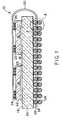
- FIG. 1is an elevation view of module 10 devised in accordance with a preferred embodiment of the present invention.
- FIG. 2is an elevation view of module 10 devised in accordance with an alternative preferred embodiment of the present invention.
- FIG. 3is an elevation view of module 10 devised in accordance with an alternative preferred embodiment of the present invention.
- FIG. 4is an elevation view of module 10 devised in accordance with an alternative preferred embodiment of the present invention.
- FIG. 5is an elevation view of module 10 devised in accordance with an alternative preferred embodiment of the present invention.
- FIG. 6is an elevation view of module 10 devised in accordance with an alternative preferred embodiment of the present invention.
- FIG. 7is still another view of an alternative embodiment devised in accordance with the invention.
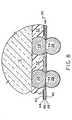
- FIG. 8depicts, in enlarged view, the area marked “A” in FIG. 1 .
- FIG. 9is an enlarged detail of an exemplar connection in a preferred embodiment of the present invention.
- FIG. 10is an elevation view of a preferred embodiment devised in accordance with the present invention.
- FIG. 11is an enlarged depiction of a part of the view of FIG. 10 .
- FIG. 12depicts, in enlarged view, the area marked “B” in FIG. 11 .
- FIG. 13depicts in enlarged view, an alternative connection strategy between constituent elements of the module and a flex in a preferred embodiment in accordance with the present invention.
- FIG. 14is an enlarged depiction of an exemplar area around a base flex contact in a preferred embodiment of the present invention.
- FIG. 15depicts an exemplar first conductive layer of a flex employed in a preferred embodiment of the invention.
- FIG. 16depicts an exemplar second conductive layer of a flex employed in a preferred embodiment of the invention.
- FIG. 1is an elevation view of module 10 devised in accordance with a preferred embodiment of the present invention.
- FIG. 1depicts a three-element preferred embodiment of the invention. The invention may, however, be employed with greater or fewer than three IC elements.
- Module 10is comprised of a base element 12 and support elements 14 and 16 .
- base element 12 and support elements 14 and 16are shown as CSP devices, but the invention is not limited to arrangements of CSPs and may be employed to aggregate a variety of package types.
- Base element 12 and support elements 14 and 16each have, in the depicted embodiment, upper surfaces 18 and lower surfaces 20 and peripheral or lateral sides 22 .
- Lateral sides 22may be in the character of sides or may, if the CSP is especially thin, be in the character of an edge.
- the present inventionmay be employed with packaged ICs that do not exhibit what would be considered a lateral side 22 such as, for example, die that are packaged to have edge-wise protective layers or coatings and a connective structure across the bottom surface of the die while leaving uncovered the upper surface of the die.
- Such packagesare employed in DRAM circuitry and may be aggregated using the present invention.
- CSPschip scale packaged integrated circuits
- FIG. 1the elevation view of FIG. 1 is depicted with CSPs of a particular profile, but it should be understood that the figures are exemplary only.
- the inventionmay be employed to advantage with many of the wide range of CSP and leaded package configurations available in the art.
- One preferred embodiment of the inventionemploys a CSP microprocessor as base element 12 and memory circuits packaged in a variety of configurations as support elements 14 and 16 , but those of skill in the art will recognize that the invention may be employed to advantage with logic and computing circuits where reduction of PWB or other board surface area consumption is desired.
- CSPssuch as, for example, ball-grid-array (“BGA”), micro-ball-grid array, and fine-pitch ball grid array (“FBGA”) packages have an array of connective contacts embodied, for example, as bumps, solder balls, or balls that extend from lower surface 20 of a plastic casing in any of several patterns and pitches. An external portion of the connective contacts is often finished with a ball of solder. Shown in FIG. 1 are CSP contacts 26 along lower surfaces 20 of elements 12 , 14 , and 16 . Contact with the integrated circuit within the respective packages is provided by CSP contacts 26 .
- BGAball-grid-array
- FBGAfine-pitch ball grid array
- FIG. 1depicts base element 12 and support elements 14 and 16 in a stacked disposition with upper major surfaces of the constituent elements being proximally located in this back to back configuration. Between upper sides 18 of support elements 14 and 16 and upper side 18 of base element 12 is shown adhesive layer 25 shown in exaggerated scale for clarity of depiction. CSP contacts 26 are emergent from lower side 20 of base element 12 and support elements 14 and 16 . Module contacts 28 are shown depicted along the bottom of module 10 and provide connection for the module to a PWB or PCB or other mounting site.
- flex circuit(“flex”, “flex circuit”, “flexible circuit structure”) 30 is shown partially wrapped about base element 12 and support elements 14 and 16 .
- Any flexible or conformable substrate with a multiple internal layer connectivity capabilitymay be used as a flex circuit in the invention.
- Some embodimentsmay employ more than one flex.
- the entire flex circuitmay be flexible or, as those of skill in the art will recognize, a PCB structure made flexible in certain areas to allow conformability in some areas and rigid in other areas for planarity along contact surfaces may be employed as an alternative flex circuit in the present invention.
- structures known as rigid-flexmay be employed.
- Support elements 14 and 16are preferably fixed to upper surface 18 of base element 12 by adhesive 25 which is shown as a tape adhesive, but may be a liquid adhesive or may be placed in discrete locations across the package.
- adhesive 25is thermally conductive.
- Adhesives that include a fluxmay be used to advantage in assembly of module 10 .
- Layer 25may also be a thermally conductive medium to encourage heat flow between the elements of module 10 .
- a mechanical clamp or clampsmay be used to hold the base and support elements together. Differing embodiments of the invention will place one or more support elements in a stacked disposition relative to a base element.
- the contacts for the module itselfmay be closer to either the base element or the support element(s) of the module although more typically and preferably, the module contacts will be closer to the base element.
- the support elementsmay also extend over the edges of the base element or may be disposed within the perimeter of the base element.
- Flex circuit 30is, in a preferred embodiment, a multi-layer flexible circuit structure that has at least two conductive layers. Other embodiments may employ, if the circuit is simple enough, a flex with one conductive layer. Preferably, the conductive layers are copper. The use of plural conductive layers provides connection advantages that simplify the interconnection schemes used to interconnect elements 12 , 14 and 16 . Multiple conductive layers also provide the opportunity, when there is sufficient routing area available, to manage capacitance and inductance issues better than a single conductive layer.
- FIG. 2shows a module 10 devised in accordance with an alternative preferred embodiment of the invention.
- FIG. 2illustrates the aggregation of a leaded package device having leads 31 (i.e., as support element 16 in this embodiment) with base element 12 and support element 14 .
- FIG. 2further depicts the placement of flex 30 attached to the upper side of base element 12 with the placement of support elements 14 and 16 in a position relatively above flex 30 rather than below as earlier shown in FIG. 1 .
- Flex 30is preferably attached to upper side 18 of base element 12 with a thermally conductive adhesive depicted by reference 25 in FIG. 2 .
- a conformal media 32is indicated in FIG. 2 as being placed between CSP contacts 26 to assist in creating conformality of structural areas of module 10 .
- conformal media 32is thermally conductive and is placed along the lower surface 20 of base element 12 although to preserve clarity of the view, its placement between only a few CSP contacts 26 of base element 12 is shown in the FIG. 2 .
- FIG. 3depicts another alternative embodiment of the present invention. Shown are base element 12 and support element 14 . In the place of previously shown single package support element 16 is leaded stack 17 , consisting of upper IC 19 and lower IC 21 . In this embodiment, stack 17 is configured in conformity with a product of the assignee of the present invention but is intended to be an exemplar and not a limiting configuration.
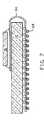
- FIG. 4illustrates an alternative preferred embodiment of the present invention in which a base element 12 is aggregated with a leaded support element 16 .
- FIG. 5depicts an alternative preferred embodiment of the present invention. Shown in FIG. 5 is a back-to-back embodiment with base element 12 having mounted upon its upper side 18 , a support element 16 configured in CSP.
- FIG. 6depicts a preferred embodiment of the present invention that employs a CSP base element 12 and CSP support elements 14 and 16 interconnected with flex 30 .
- Heat sink 34is disposed between base element 12 and support elements 14 and 16 . As shown in FIG. 6 , heat sink 34 is in contact with a portion of casing 36 of an application in which module 10 is employed.
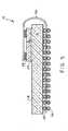
- FIG. 7illustrates an alternative preferred embodiment of the invention employed to aggregate leaded packages.
- Depicted base element 12is a leaded device while support element 16 is also a leaded device.
- FIG. 8depicts in enlarged view, the area marked “A” in FIG. 1 .
- FIG. 8illustrates the connection between example CSP contacts 26 and module contacts 28 through flex 30 .
- a depicted preferred construction for flex 30is shown in FIG. 8 to be comprised of multiple layers.
- Flex 30has a first outer surface 40 and a second outer surface 42 .
- Flex circuit 30has at least two conductive layers interior to first and second outer surfaces 40 and 42 . There may be more than two conductive layers in flex 30 . Further, two flex circuits may supplant flex 30 with each wrapping about an opposite side of the assembly.
- first conductive layer 44is at the first conductive layer level of flex 30 while second conductive layer 48 is at the second conductive layer level of flex 30 .
- both conductive layersare interior to first and second outer surfaces 40 and 42 .
- Intermediate layer 46lies between first conductive layer 44 and second conductive layer 48 .
- base flex contact 54is preferably comprised from metal at the level of second conductive layer 48 interior to second outer surface 42 .
- Base flex contact 54is solid metal in a preferred embodiment and is preferably comprised of copper and suitable barrier metals or coatings as required. This results in a solid metal pathway from element 12 to an application board thereby providing a significant thermal pathway for dissipation of heat generated in module 10 .
- This depiction of base flex contact 54illustrates the solid metal path from element 12 to module contact 28 and, therefore, to an application PWB to which module 10 is connectable. As those of skill in the art will understand, heat transference from module 10 is thereby encouraged.
- CSP contact 26 and module contact 28together offset module 10 from an application platform such as a PWB.
- the combined heights of CSP contact 26 and module contact 28provide a moment arm longer than the height of a single CSP contact 26 alone. This provides a longer moment arm through which temperature-gradient-over-time stresses (such as typified by temp cycle), can be distributed and can be helpful particularly where element 12 contacts such as CSP contacts 26 become diminutive as a result of high density contact arrays resulting in small diameter CSP contacts.
- FIG. 9is an enlarged detail of an exemplar connection between example CSP contact 26 and example module contact 28 through base flex contact 54 to illustrate the solid metal path from element 12 to module contact 28 and, therefore, to an application PWB to which module 10 is connectable.
- base flex contact 54is at the level of second conductive layer 48 and is interior to first and second outer surface layers 40 and 42 respectively, of flex circuit 30 .
- Base flex contacts 54need not be at the level of second conductive layer 48 and may be configured from first conductive layer 44 depending upon the routing demands of the interconnections specified between elements 12 and 14 or 12 and 14 and 16 .
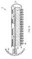
- FIG. 10is an alternative preferred embodiment of the present invention. Depicted in FIG. 10 are base element 12 and support elements 14 and 16 with all of the depicted ICs being packaged in CSP with support elements 14 and 16 extending beyond the physical boundaries of base element 12 . Also shown is extensive and preferred use of conformal underfill 32 .
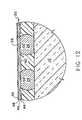
- FIG. 11is an enlarged section of the preferred embodiment depicted in FIG. 10 and identifies an area “B” that will be further described in FIG. 12 .
- FIG. 12illustrates in enlarged perspective, detail of the area marked “B” in FIG. 11 and illustrates an exemplar connection between example CSP contacts 26 of a support element and support flex contacts 56 of flex 30 .
- support flex contacts 56are shown as being at the level of first conductive layer 44 of flex 30 .
- FIG. 12illustrates a via 58 between the support flex contact 56 in contact with the right-most depicted CSP contact 26 and second conductive layer 48 .
- the use of vias between conductive layer levelsallows flexibility in strategies employed to connect base element 12 with support elements and allows, for example, the connection of a contact from support elements 14 or 16 to a selected module contact 28 .
- support elements 14 and/or 16will have signals that are not directly connected to base element 12 , but which have functionality relevant to the operation of entire module 10 .
- a module contact 28provides that signal connection to support element 14 or 16 without a corresponding direct connection to base element 12 .
- Such a connection strategyis shown in FIG. 13 .
- FIG. 14is an enlarged depiction of an exemplar area around a base flex contact 54 in a preferred embodiment.
- the depicted base contact 54is shown being delineated at the level of second conductive layer 48 , but the many base element contacts 54 employed to provide connection to base element 12 may be located at the level of second conductive layer 48 or first conductive layer 44 . Although it is not preferable, different base element contacts 54 for the same base element 12 may be located at different conductive layers.
- connection strategiesmay specify that some of the CSP contacts 26 of base element 12 should be connected to flex 30 through base element contacts 54 located at the level of second conductive layer 48 , while at the same time, other CSP contacts 26 of base element 12 should be connected to flex 30 through base element contacts 54 located at the level of first conductive layer 44 . It is preferable, however, to have all the contacts of base element 12 contact flex 30 at the same conductive layer level of the flex. In the FIG. 14 depiction of an example base contact 54 , however, windows 60 and 62 are opened in first and second outer surface layers 40 and 42 respectively, to provide access to a particular exemplar base flex contact 54 residing at the level of second conductive layer 48 in the flex.
- Base flex contact 54 as is shown in FIG. 14may be connected to or isolated from the conductive plane of second conductive layer 48 . Demarking a lower flex contact 54 from second conductive layer 48 is represented in FIG. 14 by demarcation gap 63 shown at second conductive layer 48 . Where a base flex contact 54 or support flex contact 56 is not completely isolated from its conductive layer, demarcation gaps do not extend completely around the flex contact.
- CSP contacts 26 of base element 12pass through a window 60 opened through first outer surface layer 40 , first conductive layer 44 , and intermediate layer 46 , to contact depicted base flex contact 54 .
- Window 62is opened through second outer surface layer 42 through which module contacts 28 pass to contact base flex contact 54 .
- window 62passes through second outer surface layer 42 as well as second conductive layer 48 and intermediate layer 46 to reach the level of first conductive layer 44 where the appropriate base flex contact is located while window 60 would pass only through first outer surface layer 40 .
- module contacts 28pass through windows 62 opened in second outer layer 42 to contact base flex contacts 54 .
- module 10can express a wider interface for address, data, and control signals than that expressed by the constituent elements 12 , 14 and 16 .
- a module contact 28may also be employed to convey separate enable signals through conductive layer levels to support elements 14 or 16 and thereby provide locations through which support elements 14 or 16 may be selectably enabled.
- impedance controlling planescan be used or return paths (power or ground) can be routed next to such traces as a coplanar waveguide.
- FIG. 15depicts an abstraction of a typical routing employed in first conductive plane 44 by the assignee of the present invention in implementing a preferred embodiment of the present invention.
- FIG. 15illustrates an abstraction of the plot employed for the conductive areas of at the level of first conductive plane 44 for the preferred embodiment depicted in FIG. 10 .
- the connective fields identified with references 64provide connections for support element 14 while connective fields identified with references 66 provide connections for support element 16 .
- Connective field 68provides connections for base element 12 .
- the connective fields 64 and 66provide support flex contacts 56 as well as traces that, combined with vias 58 , provide part of the connective facility for interconnecting support elements 14 and 16 to base element 12 .
- the viewis abstracted with many of the actual routing lines removed to assist in the clarity of the view.
- FIG. 16depicts an abstraction of a typical routing employed for conductive areas at the level of second conductive plane 48 by the assignee of the present invention in implementing a preferred embodiment of the present invention.
- FIG. 16illustrates an abstraction of the plot employed for the preferred embodiment depicted in FIG. 10 .
- FIGS. 15 and 16employed to connect base element 12 , there is illustrated an example of using vias 58 to more fully employ the two conductive layers of the preferred embodiments.
- Connective fields 65 and 67indicate vias 58 as well as traces (that are not shown in the depiction for clarity of view) that provide part of the connective facility for interconnecting support elements 14 and 16 to base element 12 .
- base element 12has a CSP contact 26 that passes through window 60 and therefore, first conductive layer 44 shown in FIG. 15 , to contact the base flex contact 54 at the level of the second conductive layer as shown in FIG. 16 .
- thisis a heuristic explanation and meant to be merely an example illustrating a feature found in some preferred embodiments of the invention.
- Base flex contact 54 at the level of second conductive layer 48is connected to a via 58 by a trace 70 .
- Via 58passes in a relatively upward direction toward the body of base element 12 .
- via 58passes upwardly through flex 30 , it contacts a conductive area at the level of first conductive layer 44 as shown in FIG. 15 by the identification of via 58 .
- Via 58is then connected to trace 72 that provides a connection network to a variety of other contacts in the depicted embodiment.
- trace 72branches to connect to another via 58 identified in the lower part of FIG. 15 .
- Vias that route through intermediate layer 46 to interconnect traces or flex contacts or conductive areas at different conductive layersmay be “on-pad” or coincident with the support or base flex contact to which they are connected. Such vias may also be “off-pad” and located near windows associated with the flex contacts from which signals are to be conveyed to another conductive layer. This provides added flexibility to connection schemes and layout routing. Another explication of the use of on-pad and off-pad vias that is suitable for use in the present invention is provided in incorporated and pending U.S. application Ser. No. 10/005,581, filed Oct. 26, 2001. Therein there is also found strategies for interconnection of elements using a multi-layer flex circuit that dedicates conductive layers to particular functions. Such a strategy may be used with the present invention where the simplicity of the interconnection allows.
- connection between conductive layers provided by viasmay be provided by any of several well-known techniques such as plated holes or solid lines or wires and need not literally be vias.
Landscapes
- Engineering & Computer Science (AREA)
- Microelectronics & Electronic Packaging (AREA)
- Power Engineering (AREA)
- Physics & Mathematics (AREA)
- Condensed Matter Physics & Semiconductors (AREA)
- General Physics & Mathematics (AREA)
- Computer Hardware Design (AREA)
- Structure Of Printed Boards (AREA)
Abstract
Description
- This application is a continuation of U.S. App. No. 10/136,890, filed May 2, 2002, pending; which application is a continuation-in-part of U.S. App. No. 10/005,581, filed Oct. 26, 2001, now U.S. Pat. No. 6,576,992 B1, issued Jun. 10, 2003. U.S. Pat. No. 6,576,992 B1 is hereby incorporated by reference for all purposes.
- The present invention relates to aggregating integrated circuits and, in particular, to stacking dissimilar integrated circuits.
- A variety of techniques are used to stack packaged integrated circuits. Some methods require special packages, while other techniques stack conventional packages. In some stacks, the leads of the packaged integrated circuits are used to create a stack, while in other systems, added structures such as rails provide all or part of the interconnection between packages. In still other techniques, flexible conductors with certain characteristics are used to selectively interconnect packaged integrated circuits.
- One major package configuration employed during the past decade has encapsulated an integrated circuit (IC) in a plastic surround typically having a rectangular configuration. The enveloped integrated circuit is connected to the application environment through leads emergent from the edge periphery of the plastic encapsulation. Such “leaded packages” have been the constituent elements most commonly employed by techniques for stacking packaged integrated circuits.
- Leaded packages play an important role in electronics, but efforts to miniaturize electronic components and assemblies have driven development of technologies that preserve circuit board surface area. Because leaded packages have leads emergent from peripheral sides of the package, leaded packages occupy more than a minimal amount of circuit board surface area. Consequently, alternatives to leaded packages have recently gained market share.
- One family of alternative packages is identified generally by the term “chip scale packaging” or CSP. These differ from leaded packages in that the CSP packages provide connection to an integrated circuit through a set of contacts (often embodied as “bumps,” “spheres,” or “balls”) arrayed across a major surface of the package. Instead of leads emergent from a peripheral side of the package, contacts are placed on a major surface and typically emerge from the planar bottom surface of the package.
- The goal of CSP is to occupy as little area as possible and, preferably, approximately the area of the encapsulated IC. Therefore, CSP contacts do not typically extend beyond the outline perimeter of the package. The absence of “leads” on package sides renders most stacking techniques devised for leaded packages inapplicable for CSP stacking.
- CSP has enabled reductions in size and weight parameters for many applications. CSP is a broad category that can include a variety of packages from larger than chip scale to die-sized packages such as the die-sized ball grid array (DSBGA) described in proposed JEDEC standard 95-1 for DSBGA.
- To meet the continuing demands for cost and form factor reduction with increasing memory capacities, CSP technologies that aggregate integrated circuits in CSP technology have recently been developed. For example, Sharp, Hitachi, Mitsubishi and Intel recently undertook support of what are called the S-CSP specifications for flash and SRAM applications. Those S-CSP specifications describe, however, stacking multiple die within a single chip scale package and do not provide a technology for stacking chip scale packages. Stacking integrated circuits within a single package requires specialized technology that includes reformulation of package internals and significant expense with possible supply chain vulnerabilities.
- There are several known techniques for stacking packages articulated in chip scale technology. The assignee of the present invention has developed previous systems for aggregating FBGA packages in space saving topologies. The assignee of the present invention has systems for stacking BGA packages on a DIMM in a RAMBUS environment.
- In U.S. Pat. No. 6,205,654 B1, owned by the assignee of the present invention, a system for stacking ball grid array packages that employs lead carriers to extend connectable points out from the packages is described. Other known techniques add structures to a stack of BGA-packaged ICs. Still others aggregate CSPs on a DIMM with angular placement of the packages. Such techniques provide alternatives, but require topologies of added cost and complexity.
- U.S. Pat. No. 6,262,895 Bi to Forthun (the “Forthun patent”) purports to disclose a technique for stacking chip scale packaged ICs. The Forthun patent discloses a “package” that exhibits a flex circuit wrapped partially about a CSP. The flex circuit is said to have pad arrays on upper and lower surfaces of the flex.
- The flex circuit of the Forthun “package” has a pad array on its upper surface and a pad array centrally located upon its lower surface. On the lower surface of the flex there are third and fourth arrays on opposite sides from the central lower surface pad array. To create the package of Forthun, a CSP contacts the pad array located on the upper surface of the flex circuit. As described in the Forthun patent, the contacts on the lower surface of the CSP are pushed through “slits” in the upper surface pads and advanced through the flex to protrude from the pads of the lower surface array and, therefore, the bottom surface of the package. Thus, the contacts of the CSP serve as the contacts for the package. The sides of the flex are partially wrapped about the CSP to adjacently place the third and fourth pad arrays above the upper major surface of the CSP to create from the combination of the third and fourth pad arrays, a fifth pad array for connection to another such package. Thus, as described in the Forthun disclosure, a stacked module of CSPs created with the described packages will exhibit a flex circuit wrapped about each CSP in the module.
- Most previous known methods for stacking aggregate similarly packaged integrated circuits. What is needed are methods and structures for stacking dissimilar packages and circuits in thermally efficient, reliable structures.
- The present invention stacks packaged integrated circuits into modules that conserve PWB or other board surface area. The invention provides techniques and structures for aggregating chip scale-packaged integrated circuits (CSPs) or leaded packages with other CSPs or with monolithic or stacked leaded packages into modules that conserve PWB or other board surface area. The present invention can be used to advantage with CSP or leaded packages of a variety of sizes and configurations ranging from larger packaged base elements having many dozens of contacts to smaller packages such as, for example, die-sized packages such as DSBGA. Although the present invention is applied most frequently to packages that contain one die, it may be employed with packages that include more than one integrated circuit die.
- In a preferred embodiment devised in accordance with the present invention, a base element IC and a support element IC are aggregated through a flex circuit having two conductive layers that are patterned to selectively connect the two IC elements. Simpler embodiments may use a one conductive layer flex. A portion of the flex circuit connected to the support element is folded over the base element to dispose the support element above the base element while reducing the overall footprint occupied by the two ICs. The flex circuit connects the ICs and provides a thermal and electrical connection path between the module and an application environment such as a printed wiring board (PWB).
- The present invention may be employed to advantage in numerous configurations and combinations in modules provided for high-density memories, high capacity computing, or particular applications where small size is valued.
FIG. 1 is an elevation view ofmodule 10 devised in accordance with a preferred embodiment of the present invention.FIG. 2 is an elevation view ofmodule 10 devised in accordance with an alternative preferred embodiment of the present invention.FIG. 3 is an elevation view ofmodule 10 devised in accordance with an alternative preferred embodiment of the present invention.FIG. 4 is an elevation view ofmodule 10 devised in accordance with an alternative preferred embodiment of the present invention.FIG. 5 is an elevation view ofmodule 10 devised in accordance with an alternative preferred embodiment of the present invention.FIG. 6 is an elevation view ofmodule 10 devised in accordance with an alternative preferred embodiment of the present invention.FIG. 7 is still another view of an alternative embodiment devised in accordance with the invention.FIG. 8 depicts, in enlarged view, the area marked “A” inFIG. 1 .FIG. 9 is an enlarged detail of an exemplar connection in a preferred embodiment of the present invention.FIG. 10 is an elevation view of a preferred embodiment devised in accordance with the present invention.FIG. 11 is an enlarged depiction of a part of the view ofFIG. 10 .FIG. 12 depicts, in enlarged view, the area marked “B” inFIG. 11 .FIG. 13 depicts in enlarged view, an alternative connection strategy between constituent elements of the module and a flex in a preferred embodiment in accordance with the present invention.FIG. 14 is an enlarged depiction of an exemplar area around a base flex contact in a preferred embodiment of the present invention.FIG. 15 depicts an exemplar first conductive layer of a flex employed in a preferred embodiment of the invention.FIG. 16 depicts an exemplar second conductive layer of a flex employed in a preferred embodiment of the invention.FIG. 1 is an elevation view ofmodule 10 devised in accordance with a preferred embodiment of the present invention.FIG. 1 depicts a three-element preferred embodiment of the invention. The invention may, however, be employed with greater or fewer than three IC elements.Module 10 is comprised of abase element 12 andsupport elements base element 12 andsupport elements Base element 12 andsupport elements upper surfaces 18 andlower surfaces 20 and peripheral or lateral sides22.Lateral sides 22 may be in the character of sides or may, if the CSP is especially thin, be in the character of an edge. For example, in addition to the well known leaded and CSP packages, the present invention may be employed with packaged ICs that do not exhibit what would be considered alateral side 22 such as, for example, die that are packaged to have edge-wise protective layers or coatings and a connective structure across the bottom surface of the die while leaving uncovered the upper surface of the die. Such packages are employed in DRAM circuitry and may be aggregated using the present invention.- The invention is employed to advantage with a variety of combinations of packages including leaded and CSP and other configurations of packaged ICs. CSPs of a variety of types and configurations such as, for example, those that are larger than die-sized, as well those that are at or near die size as well as the variety of ball grid array packages known in the art may be employed to advantage by the invention. Collectively, these will be known herein as chip scale packaged integrated circuits (CSPs) and some preferred embodiments will be described in terms of CSPs, but the particular configurations used in the explanatory figures are not, however, to be construed as limiting. For example, the elevation view of
FIG. 1 is depicted with CSPs of a particular profile, but it should be understood that the figures are exemplary only. Later figures show embodiments of the invention that employ CSPs of other configurations aggregated with leaded packages as an example of some of the many alternative IC package configurations and combinations with which the invention may be employed. The system of the invention may also be employed with leaded packages while the module itself presents an array of bumps or balls to the application environment. - The invention may be employed to advantage with many of the wide range of CSP and leaded package configurations available in the art. One preferred embodiment of the invention employs a CSP microprocessor as
base element 12 and memory circuits packaged in a variety of configurations assupport elements - Typical CSPs, such as, for example, ball-grid-array (“BGA”), micro-ball-grid array, and fine-pitch ball grid array (“FBGA”) packages have an array of connective contacts embodied, for example, as bumps, solder balls, or balls that extend from
lower surface 20 of a plastic casing in any of several patterns and pitches. An external portion of the connective contacts is often finished with a ball of solder. Shown inFIG. 1 areCSP contacts 26 alonglower surfaces 20 ofelements CSP contacts 26. FIG. 1 depictsbase element 12 andsupport elements upper sides 18 ofsupport elements upper side 18 ofbase element 12 is shownadhesive layer 25 shown in exaggerated scale for clarity of depiction.CSP contacts 26 are emergent fromlower side 20 ofbase element 12 andsupport elements Module contacts 28 are shown depicted along the bottom ofmodule 10 and provide connection for the module to a PWB or PCB or other mounting site.- In
FIG. 1 , flex circuit (“flex”, “flex circuit”, “flexible circuit structure”)30 is shown partially wrapped aboutbase element 12 andsupport elements Support elements upper surface 18 ofbase element 12 by adhesive25 which is shown as a tape adhesive, but may be a liquid adhesive or may be placed in discrete locations across the package. Preferably, adhesive25 is thermally conductive. Adhesives that include a flux may be used to advantage in assembly ofmodule 10.Layer 25 may also be a thermally conductive medium to encourage heat flow between the elements ofmodule 10. Alternatively, a mechanical clamp or clamps may be used to hold the base and support elements together. Differing embodiments of the invention will place one or more support elements in a stacked disposition relative to a base element. The contacts for the module itself may be closer to either the base element or the support element(s) of the module although more typically and preferably, the module contacts will be closer to the base element. The support elements may also extend over the edges of the base element or may be disposed within the perimeter of the base element.Flex circuit 30 is, in a preferred embodiment, a multi-layer flexible circuit structure that has at least two conductive layers. Other embodiments may employ, if the circuit is simple enough, a flex with one conductive layer. Preferably, the conductive layers are copper. The use of plural conductive layers provides connection advantages that simplify the interconnection schemes used to interconnectelements FIG. 2 shows amodule 10 devised in accordance with an alternative preferred embodiment of the invention.FIG. 2 illustrates the aggregation of a leaded package device having leads31 (i.e., assupport element 16 in this embodiment) withbase element 12 andsupport element 14.FIG. 2 further depicts the placement offlex 30 attached to the upper side ofbase element 12 with the placement ofsupport elements flex 30 rather than below as earlier shown inFIG. 1 .Flex 30 is preferably attached toupper side 18 ofbase element 12 with a thermally conductive adhesive depicted byreference 25 inFIG. 2 . Aconformal media 32 is indicated inFIG. 2 as being placed betweenCSP contacts 26 to assist in creating conformality of structural areas ofmodule 10. Preferably,conformal media 32 is thermally conductive and is placed along thelower surface 20 ofbase element 12 although to preserve clarity of the view, its placement between only afew CSP contacts 26 ofbase element 12 is shown in theFIG. 2 .FIG. 3 depicts another alternative embodiment of the present invention. Shown arebase element 12 andsupport element 14. In the place of previously shown singlepackage support element 16 isleaded stack 17, consisting of upper IC19 andlower IC 21. In this embodiment, stack17 is configured in conformity with a product of the assignee of the present invention but is intended to be an exemplar and not a limiting configuration.FIG. 4 illustrates an alternative preferred embodiment of the present invention in which abase element 12 is aggregated with aleaded support element 16.FIG. 5 depicts an alternative preferred embodiment of the present invention. Shown inFIG. 5 is a back-to-back embodiment withbase element 12 having mounted upon itsupper side 18, asupport element 16 configured in CSP.FIG. 6 depicts a preferred embodiment of the present invention that employs aCSP base element 12 andCSP support elements flex 30.Heat sink 34 is disposed betweenbase element 12 andsupport elements FIG. 6 ,heat sink 34 is in contact with a portion of casing36 of an application in whichmodule 10 is employed.FIG. 7 illustrates an alternative preferred embodiment of the invention employed to aggregate leaded packages. Depictedbase element 12 is a leaded device whilesupport element 16 is also a leaded device.FIG. 8 depicts in enlarged view, the area marked “A” inFIG. 1 .FIG. 8 illustrates the connection betweenexample CSP contacts 26 andmodule contacts 28 throughflex 30. A depicted preferred construction forflex 30 is shown inFIG. 8 to be comprised of multiple layers.Flex 30 has a firstouter surface 40 and a secondouter surface 42.Flex circuit 30 has at least two conductive layers interior to first and secondouter surfaces flex 30. Further, two flex circuits may supplantflex 30 with each wrapping about an opposite side of the assembly. In the depicted preferred embodiment, firstconductive layer 44 is at the first conductive layer level offlex 30 while secondconductive layer 48 is at the second conductive layer level offlex 30. Typically, both conductive layers are interior to first and secondouter surfaces Intermediate layer 46 lies between firstconductive layer 44 and secondconductive layer 48. There may be more than one intermediate layer, but an intermediate layer of polyimide is preferred. Similar dielectric materials may be used.- As depicted in
FIG. 8 and seen in more detail in later figures,base flex contact 54 is preferably comprised from metal at the level of secondconductive layer 48 interior to secondouter surface 42.Base flex contact 54 is solid metal in a preferred embodiment and is preferably comprised of copper and suitable barrier metals or coatings as required. This results in a solid metal pathway fromelement 12 to an application board thereby providing a significant thermal pathway for dissipation of heat generated inmodule 10. This depiction ofbase flex contact 54 illustrates the solid metal path fromelement 12 tomodule contact 28 and, therefore, to an application PWB to whichmodule 10 is connectable. As those of skill in the art will understand, heat transference frommodule 10 is thereby encouraged. - With continuing reference to
FIG. 8 ,CSP contact 26 andmodule contact 28 together offsetmodule 10 from an application platform such as a PWB. The combined heights ofCSP contact 26 andmodule contact 28 provide a moment arm longer than the height of asingle CSP contact 26 alone. This provides a longer moment arm through which temperature-gradient-over-time stresses (such as typified by temp cycle), can be distributed and can be helpful particularly whereelement 12 contacts such asCSP contacts 26 become diminutive as a result of high density contact arrays resulting in small diameter CSP contacts. FIG. 9 is an enlarged detail of an exemplar connection betweenexample CSP contact 26 andexample module contact 28 throughbase flex contact 54 to illustrate the solid metal path fromelement 12 tomodule contact 28 and, therefore, to an application PWB to whichmodule 10 is connectable. As shown inFIG. 9 ,base flex contact 54 is at the level of secondconductive layer 48 and is interior to first and second outer surface layers40 and42 respectively, offlex circuit 30.Base flex contacts 54 need not be at the level of secondconductive layer 48 and may be configured from firstconductive layer 44 depending upon the routing demands of the interconnections specified betweenelements FIG. 10 is an alternative preferred embodiment of the present invention. Depicted inFIG. 10 arebase element 12 andsupport elements support elements base element 12. Also shown is extensive and preferred use ofconformal underfill 32.FIG. 11 is an enlarged section of the preferred embodiment depicted inFIG. 10 and identifies an area “B” that will be further described inFIG. 12 .FIG. 12 illustrates in enlarged perspective, detail of the area marked “B” inFIG. 11 and illustrates an exemplar connection betweenexample CSP contacts 26 of a support element andsupport flex contacts 56 offlex 30. In this depiction,support flex contacts 56 are shown as being at the level of firstconductive layer 44 offlex 30.FIG. 12 illustrates a via58 between thesupport flex contact 56 in contact with the right-most depictedCSP contact 26 and secondconductive layer 48. The use of vias between conductive layer levels allows flexibility in strategies employed to connectbase element 12 with support elements and allows, for example, the connection of a contact fromsupport elements module contact 28. Often,support elements 14 and/or16 will have signals that are not directly connected tobase element 12, but which have functionality relevant to the operation ofentire module 10. In such cases, amodule contact 28 provides that signal connection to supportelement base element 12. Such a connection strategy is shown inFIG. 13 .FIG. 14 is an enlarged depiction of an exemplar area around abase flex contact 54 in a preferred embodiment. The depictedbase contact 54 is shown being delineated at the level of secondconductive layer 48, but the manybase element contacts 54 employed to provide connection tobase element 12 may be located at the level of secondconductive layer 48 or firstconductive layer 44. Although it is not preferable, differentbase element contacts 54 for thesame base element 12 may be located at different conductive layers. That is, some connection strategies may specify that some of theCSP contacts 26 ofbase element 12 should be connected to flex30 throughbase element contacts 54 located at the level of secondconductive layer 48, while at the same time,other CSP contacts 26 ofbase element 12 should be connected to flex30 throughbase element contacts 54 located at the level of firstconductive layer 44. It is preferable, however, to have all the contacts ofbase element 12contact flex 30 at the same conductive layer level of the flex. In theFIG. 14 depiction of anexample base contact 54, however,windows base flex contact 54 residing at the level of secondconductive layer 48 in the flex.Base flex contact 54 as is shown inFIG. 14 may be connected to or isolated from the conductive plane of secondconductive layer 48. Demarking alower flex contact 54 from secondconductive layer 48 is represented inFIG. 14 bydemarcation gap 63 shown at secondconductive layer 48. Where abase flex contact 54 orsupport flex contact 56 is not completely isolated from its conductive layer, demarcation gaps do not extend completely around the flex contact.- As shown by example in
FIG. 14 ,CSP contacts 26 ofbase element 12 pass through awindow 60 opened through firstouter surface layer 40, firstconductive layer 44, andintermediate layer 46, to contact depictedbase flex contact 54.Window 62 is opened through secondouter surface layer 42 through whichmodule contacts 28 pass to contactbase flex contact 54. Where thebase flex contact 54 to be contacted is at the level of firstconductive layer 44,window 62 passes through secondouter surface layer 42 as well as secondconductive layer 48 andintermediate layer 46 to reach the level of firstconductive layer 44 where the appropriate base flex contact is located whilewindow 60 would pass only through firstouter surface layer 40. As earlier shown inFIG. 13 , there need not be awindow 60 for everywindow 62 where amodule contact 28 provides connection only to a support element. Similarly, there need not be awindow 62 for everywindow 60 when there is nomodule contact 28 in physical proximity to aparticular base element 12 CSP contact. Wherebase element 12 is a leaded package, pads connected by vias to appropriate conductive layers are employed withflex 30. - With continuing reference to
FIGS. 13 and 14 ,module contacts 28 pass throughwindows 62 opened in secondouter layer 42 to contactbase flex contacts 54. In those embodiments such as that shown inFIG. 13 that showmodule 10 exhibiting an array ofmodule contacts 28 having a greater number ofmodule contacts 28 than thebase element 12 exhibits in CSP orother contacts 26,module 10 can express a wider interface for address, data, and control signals than that expressed by theconstituent elements module contact 28 may also be employed to convey separate enable signals through conductive layer levels to supportelements elements - Depending upon the frequencies employed by the elements of
module 10, the dedication of one of the conductive layers offlex 30 to a particular functionality such as ground or power is typically not required for lower frequency applications. In other applications where higher speeds are encountered or where longer trace lengths beyond the critical length are employed, impedance controlling planes can be used or return paths (power or ground) can be routed next to such traces as a coplanar waveguide. FIG. 15 depicts an abstraction of a typical routing employed in firstconductive plane 44 by the assignee of the present invention in implementing a preferred embodiment of the present invention.FIG. 15 illustrates an abstraction of the plot employed for the conductive areas of at the level of firstconductive plane 44 for the preferred embodiment depicted inFIG. 10 . As those of skill will notice, in the plot shown inFIG. 15 , the connective fields identified withreferences 64 provide connections forsupport element 14 while connective fields identified withreferences 66 provide connections forsupport element 16.Connective field 68 provides connections forbase element 12. Theconnective fields support flex contacts 56 as well as traces that, combined withvias 58, provide part of the connective facility for interconnectingsupport elements base element 12. The view is abstracted with many of the actual routing lines removed to assist in the clarity of the view.FIG. 16 depicts an abstraction of a typical routing employed for conductive areas at the level of secondconductive plane 48 by the assignee of the present invention in implementing a preferred embodiment of the present invention.FIG. 16 illustrates an abstraction of the plot employed for the preferred embodiment depicted inFIG. 10 .- In the area of
FIGS. 15 and 16 employed to connectbase element 12, there is illustrated an example of usingvias 58 to more fully employ the two conductive layers of the preferred embodiments.Connective fields vias 58 as well as traces (that are not shown in the depiction for clarity of view) that provide part of the connective facility for interconnectingsupport elements base element 12. - On the depiction of
FIG. 16 , there is found the identification of abase flex contact 54. With reference to earlierFIGS. 13 and 14 ,base element 12 has aCSP contact 26 that passes throughwindow 60 and therefore, firstconductive layer 44 shown inFIG. 15 , to contact thebase flex contact 54 at the level of the second conductive layer as shown inFIG. 16 . It should be understood that this is a heuristic explanation and meant to be merely an example illustrating a feature found in some preferred embodiments of the invention. Base flex contact 54 at the level of secondconductive layer 48 is connected to a via58 by atrace 70. Via58 passes in a relatively upward direction toward the body ofbase element 12. As via58 passes upwardly throughflex 30, it contacts a conductive area at the level of firstconductive layer 44 as shown inFIG. 15 by the identification of via58. Via58 is then connected to trace72 that provides a connection network to a variety of other contacts in the depicted embodiment. For example, trace72 branches to connect to another via58 identified in the lower part ofFIG. 15 . Thus, the use of two conductive layers is given an added flexibility by the illustrated use of vias through an intermediate layer.- Vias that route through
intermediate layer 46 to interconnect traces or flex contacts or conductive areas at different conductive layers may be “on-pad” or coincident with the support or base flex contact to which they are connected. Such vias may also be “off-pad” and located near windows associated with the flex contacts from which signals are to be conveyed to another conductive layer. This provides added flexibility to connection schemes and layout routing. Another explication of the use of on-pad and off-pad vias that is suitable for use in the present invention is provided in incorporated and pending U.S. application Ser. No. 10/005,581, filed Oct. 26, 2001. Therein there is also found strategies for interconnection of elements using a multi-layer flex circuit that dedicates conductive layers to particular functions. Such a strategy may be used with the present invention where the simplicity of the interconnection allows. - As those of skill will recognize, the connection between conductive layers provided by vias (on or off pad) may be provided by any of several well-known techniques such as plated holes or solid lines or wires and need not literally be vias.
- Although the present invention has been described in detail, it will be apparent to those skilled in the art that the invention may be embodied in a variety of specific forms and that various changes, substitutions and alterations can be made without departing from the spirit and scope of the invention. The described embodiments are only illustrative and not restrictive and the scope of the invention is, therefore, indicated by the following claims.
Claims (30)
Priority Applications (1)
| Application Number | Priority Date | Filing Date | Title |
|---|---|---|---|
| US10/958,934US7335975B2 (en) | 2001-10-26 | 2004-10-05 | Integrated circuit stacking system and method |
Applications Claiming Priority (3)
| Application Number | Priority Date | Filing Date | Title |
|---|---|---|---|
| US10/005,581US6576992B1 (en) | 2001-10-26 | 2001-10-26 | Chip scale stacking system and method |
| US10/136,890US6940729B2 (en) | 2001-10-26 | 2002-05-02 | Integrated circuit stacking system and method |
| US10/958,934US7335975B2 (en) | 2001-10-26 | 2004-10-05 | Integrated circuit stacking system and method |
Related Parent Applications (1)
| Application Number | Title | Priority Date | Filing Date |
|---|---|---|---|
| US10/136,890ContinuationUS6940729B2 (en) | 2001-10-26 | 2002-05-02 | Integrated circuit stacking system and method |
Publications (2)
| Publication Number | Publication Date |
|---|---|
| US20050041404A1true US20050041404A1 (en) | 2005-02-24 |
| US7335975B2 US7335975B2 (en) | 2008-02-26 |
Family
ID=34197351
Family Applications (4)
| Application Number | Title | Priority Date | Filing Date |
|---|---|---|---|
| US10/136,890Expired - LifetimeUS6940729B2 (en) | 2001-10-26 | 2002-05-02 | Integrated circuit stacking system and method |
| US10/958,934Expired - LifetimeUS7335975B2 (en) | 2001-10-26 | 2004-10-05 | Integrated circuit stacking system and method |
| US10/958,924Expired - LifetimeUS7586758B2 (en) | 2001-10-26 | 2004-10-05 | Integrated circuit stacking system |
| US10/958,584Expired - LifetimeUS7606048B2 (en) | 2001-10-26 | 2004-10-05 | Integrated circuit stacking system |
Family Applications Before (1)
| Application Number | Title | Priority Date | Filing Date |
|---|---|---|---|
| US10/136,890Expired - LifetimeUS6940729B2 (en) | 2001-10-26 | 2002-05-02 | Integrated circuit stacking system and method |
Family Applications After (2)
| Application Number | Title | Priority Date | Filing Date |
|---|---|---|---|
| US10/958,924Expired - LifetimeUS7586758B2 (en) | 2001-10-26 | 2004-10-05 | Integrated circuit stacking system |
| US10/958,584Expired - LifetimeUS7606048B2 (en) | 2001-10-26 | 2004-10-05 | Integrated circuit stacking system |
Country Status (1)
| Country | Link |
|---|---|
| US (4) | US6940729B2 (en) |
Cited By (4)
| Publication number | Priority date | Publication date | Assignee | Title |
|---|---|---|---|---|
| US20050233496A1 (en)* | 2003-05-30 | 2005-10-20 | Tessera, Inc. | Method of making assemblies having stacked semiconductor chips |
| CN102238324A (en)* | 2010-05-06 | 2011-11-09 | 佳能株式会社 | Electronic device |
| CN102256435A (en)* | 2010-05-21 | 2011-11-23 | 富士通株式会社 | Multilayer printed circuit board using flexible interconnect structure, and method of making same |
| US20130201620A1 (en)* | 2012-02-06 | 2013-08-08 | Alexander D. Schlaupitz | Flexible Circuit Connectors with Reduced Profiles |
Families Citing this family (96)
| Publication number | Priority date | Publication date | Assignee | Title |
|---|---|---|---|---|
| US6323060B1 (en) | 1999-05-05 | 2001-11-27 | Dense-Pac Microsystems, Inc. | Stackable flex circuit IC package and method of making same |
| US6262895B1 (en) | 2000-01-13 | 2001-07-17 | John A. Forthun | Stackable chip package with flex carrier |
| JP2001237280A (en)* | 2000-02-22 | 2001-08-31 | Nec Corp | Tape carrier type semiconductor device and flexible film connection board |
| US6914324B2 (en)* | 2001-10-26 | 2005-07-05 | Staktek Group L.P. | Memory expansion and chip scale stacking system and method |
| US20030234443A1 (en) | 2001-10-26 | 2003-12-25 | Staktek Group, L.P. | Low profile stacking system and method |
| US7371609B2 (en) | 2001-10-26 | 2008-05-13 | Staktek Group L.P. | Stacked module systems and methods |
| US20060255446A1 (en) | 2001-10-26 | 2006-11-16 | Staktek Group, L.P. | Stacked modules and method |
| US7026708B2 (en)* | 2001-10-26 | 2006-04-11 | Staktek Group L.P. | Low profile chip scale stacking system and method |
| US7053478B2 (en) | 2001-10-26 | 2006-05-30 | Staktek Group L.P. | Pitch change and chip scale stacking system |
| US7310458B2 (en) | 2001-10-26 | 2007-12-18 | Staktek Group L.P. | Stacked module systems and methods |
| US6940729B2 (en) | 2001-10-26 | 2005-09-06 | Staktek Group L.P. | Integrated circuit stacking system and method |
| US20050056921A1 (en)* | 2003-09-15 | 2005-03-17 | Staktek Group L.P. | Stacked module systems and methods |
| US7202555B2 (en) | 2001-10-26 | 2007-04-10 | Staktek Group L.P. | Pitch change and chip scale stacking system and method |
| US6956284B2 (en) | 2001-10-26 | 2005-10-18 | Staktek Group L.P. | Integrated circuit stacking system and method |
| US7656678B2 (en) | 2001-10-26 | 2010-02-02 | Entorian Technologies, Lp | Stacked module systems |
| US7485951B2 (en) | 2001-10-26 | 2009-02-03 | Entorian Technologies, Lp | Modularized die stacking system and method |
| US7081373B2 (en)* | 2001-12-14 | 2006-07-25 | Staktek Group, L.P. | CSP chip stack with flex circuit |
| AU2003298595A1 (en)* | 2002-10-08 | 2004-05-04 | Chippac, Inc. | Semiconductor stacked multi-package module having inverted second package |
| JP3908671B2 (en)* | 2003-01-29 | 2007-04-25 | 松下電器産業株式会社 | Semiconductor device and display device using the same |
| US20040245615A1 (en)* | 2003-06-03 | 2004-12-09 | Staktek Group, L.P. | Point to point memory expansion system and method |
| US6995465B2 (en)* | 2003-06-04 | 2006-02-07 | Intel Corporation | Silicon building block architecture with flex tape |
| US7542304B2 (en)* | 2003-09-15 | 2009-06-02 | Entorian Technologies, Lp | Memory expansion and integrated circuit stacking system and method |
| FR2861895B1 (en)* | 2003-11-03 | 2006-02-24 | Commissariat Energie Atomique | METHOD AND DEVICE FOR CONNECTING CHIPS |
| WO2005059995A2 (en)* | 2003-12-18 | 2005-06-30 | Rf Module And Optical Design Limited | Semiconductor package with integrated heatsink and electromagnetic shield |
| WO2005067044A1 (en)* | 2004-01-12 | 2005-07-21 | Infineon Technologies Ag | A method for connecting a die assembly to a substrate in an integrated circuit and a semiconductor device comprising a die assembly |
| US7126829B1 (en) | 2004-02-09 | 2006-10-24 | Pericom Semiconductor Corp. | Adapter board for stacking Ball-Grid-Array (BGA) chips |
| US7423885B2 (en) | 2004-09-03 | 2008-09-09 | Entorian Technologies, Lp | Die module system |
| US7289327B2 (en) | 2006-02-27 | 2007-10-30 | Stakick Group L.P. | Active cooling methods and apparatus for modules |
| US7522421B2 (en) | 2004-09-03 | 2009-04-21 | Entorian Technologies, Lp | Split core circuit module |
| US7760513B2 (en) | 2004-09-03 | 2010-07-20 | Entorian Technologies Lp | Modified core for circuit module system and method |
| US7606050B2 (en) | 2004-09-03 | 2009-10-20 | Entorian Technologies, Lp | Compact module system and method |
| US7511968B2 (en) | 2004-09-03 | 2009-03-31 | Entorian Technologies, Lp | Buffered thin module system and method |
| US7606049B2 (en) | 2004-09-03 | 2009-10-20 | Entorian Technologies, Lp | Module thermal management system and method |
| US7616452B2 (en) | 2004-09-03 | 2009-11-10 | Entorian Technologies, Lp | Flex circuit constructions for high capacity circuit module systems and methods |
| US7606040B2 (en) | 2004-09-03 | 2009-10-20 | Entorian Technologies, Lp | Memory module system and method |
| US7579687B2 (en) | 2004-09-03 | 2009-08-25 | Entorian Technologies, Lp | Circuit module turbulence enhancement systems and methods |
| US7542297B2 (en) | 2004-09-03 | 2009-06-02 | Entorian Technologies, Lp | Optimized mounting area circuit module system and method |
| US7324352B2 (en) | 2004-09-03 | 2008-01-29 | Staktek Group L.P. | High capacity thin module system and method |
| US7443023B2 (en) | 2004-09-03 | 2008-10-28 | Entorian Technologies, Lp | High capacity thin module system |
| US20060050492A1 (en) | 2004-09-03 | 2006-03-09 | Staktek Group, L.P. | Thin module system and method |
| US7446410B2 (en) | 2004-09-03 | 2008-11-04 | Entorian Technologies, Lp | Circuit module with thermal casing systems |
| US7468893B2 (en) | 2004-09-03 | 2008-12-23 | Entorian Technologies, Lp | Thin module system and method |
| US8072058B2 (en)* | 2004-10-25 | 2011-12-06 | Amkor Technology, Inc. | Semiconductor package having a plurality input/output members |
| US7309914B2 (en)* | 2005-01-20 | 2007-12-18 | Staktek Group L.P. | Inverted CSP stacking system and method |
| US7709943B2 (en)* | 2005-02-14 | 2010-05-04 | Daniel Michaels | Stacked ball grid array package module utilizing one or more interposer layers |
| US20080203552A1 (en)* | 2005-02-15 | 2008-08-28 | Unisemicon Co., Ltd. | Stacked Package and Method of Fabricating the Same |
| US20060250780A1 (en)* | 2005-05-06 | 2006-11-09 | Staktek Group L.P. | System component interposer |
| US7033861B1 (en) | 2005-05-18 | 2006-04-25 | Staktek Group L.P. | Stacked module systems and method |
| JP4750492B2 (en)* | 2005-07-20 | 2011-08-17 | 富士通株式会社 | IC chip mounting method |
| US20070096333A1 (en)* | 2005-10-31 | 2007-05-03 | Amir Motamedi | Optimal stacked die organization |
| US7576995B2 (en) | 2005-11-04 | 2009-08-18 | Entorian Technologies, Lp | Flex circuit apparatus and method for adding capacitance while conserving circuit board surface area |
| US7508069B2 (en) | 2006-01-11 | 2009-03-24 | Entorian Technologies, Lp | Managed memory component |
| US7508058B2 (en) | 2006-01-11 | 2009-03-24 | Entorian Technologies, Lp | Stacked integrated circuit module |
| US7304382B2 (en) | 2006-01-11 | 2007-12-04 | Staktek Group L.P. | Managed memory component |
| US7608920B2 (en) | 2006-01-11 | 2009-10-27 | Entorian Technologies, Lp | Memory card and method for devising |
| US7605454B2 (en) | 2006-01-11 | 2009-10-20 | Entorian Technologies, Lp | Memory card and method for devising |
| US8411450B2 (en)* | 2006-01-25 | 2013-04-02 | Nec Corporation | Electronic device package, module, and electronic device |
| US7511969B2 (en) | 2006-02-02 | 2009-03-31 | Entorian Technologies, Lp | Composite core circuit module system and method |
| US7888185B2 (en) | 2006-08-17 | 2011-02-15 | Micron Technology, Inc. | Semiconductor device assemblies and systems including at least one conductive pathway extending around a side of at least one semiconductor device |
| US7425758B2 (en)* | 2006-08-28 | 2008-09-16 | Micron Technology, Inc. | Metal core foldover package structures |
| JP2008066655A (en)* | 2006-09-11 | 2008-03-21 | Matsushita Electric Ind Co Ltd | SEMICONDUCTOR DEVICE, SEMICONDUCTOR DEVICE MANUFACTURING METHOD, AND ELECTRIC DEVICE SYSTEM |
| US7468553B2 (en) | 2006-10-20 | 2008-12-23 | Entorian Technologies, Lp | Stackable micropackages and stacked modules |
| US7417310B2 (en) | 2006-11-02 | 2008-08-26 | Entorian Technologies, Lp | Circuit module having force resistant construction |
| US8018042B2 (en)* | 2007-03-23 | 2011-09-13 | Microsemi Corporation | Integrated circuit with flexible planar leads |
| US8058719B2 (en)* | 2007-03-23 | 2011-11-15 | Microsemi Corporation | Integrated circuit with flexible planer leads |
| US8050047B2 (en)* | 2007-07-12 | 2011-11-01 | Stats Chippac Ltd. | Integrated circuit package system with flexible substrate and recessed package |
| US8031475B2 (en)* | 2007-07-12 | 2011-10-04 | Stats Chippac, Ltd. | Integrated circuit package system with flexible substrate and mounded package |
| US20090079097A1 (en)* | 2007-09-25 | 2009-03-26 | Silverbrook Research Pty Ltd | Electronic component with wire bonds in low modulus fill encapsulant |
| US7944050B2 (en)* | 2008-02-06 | 2011-05-17 | Infineon Technologies Ag | Integrated circuit device and a method of making the integrated circuit device |
| US8030746B2 (en)* | 2008-02-08 | 2011-10-04 | Infineon Technologies Ag | Integrated circuit package |
| US8278141B2 (en)* | 2008-06-11 | 2012-10-02 | Stats Chippac Ltd. | Integrated circuit package system with internal stacking module |
| US8539408B1 (en) | 2008-07-29 | 2013-09-17 | Clarkson University | Method for thermal simulation |
| US7697281B2 (en) | 2008-09-05 | 2010-04-13 | Apple Inc. | Handheld computing device |
| US7869206B2 (en) | 2008-09-05 | 2011-01-11 | Apple Inc. | Handheld computing device |
| JP2010225943A (en)* | 2009-03-24 | 2010-10-07 | Toshiba Corp | Semiconductor device |
| US8451620B2 (en) | 2009-11-30 | 2013-05-28 | Micron Technology, Inc. | Package including an underfill material in a portion of an area between the package and a substrate or another package |
| US8217507B1 (en)* | 2010-01-22 | 2012-07-10 | Amkor Technology, Inc. | Edge mount semiconductor package |
| TWI406376B (en)* | 2010-06-15 | 2013-08-21 | Powertech Technology Inc | Semiconductor chip package |
| US8634204B2 (en) | 2010-08-19 | 2014-01-21 | Apple Inc. | Compact folded configuration for integrated circuit packaging |
| US8391010B2 (en) | 2010-08-19 | 2013-03-05 | Apple Inc. | Internal frame optimized for stiffness and heat transfer |
| US9602914B2 (en) | 2010-08-27 | 2017-03-21 | Apple Inc. | Porting audio using a connector in a small form factor electronic device |
| US8515113B2 (en) | 2010-08-19 | 2013-08-20 | Apple Inc. | Composite microphone boot to optimize sealing and mechanical properties |
| US8427379B2 (en) | 2010-08-19 | 2013-04-23 | Apple Inc. | Modular material antenna assembly |
| US8477492B2 (en) | 2010-08-19 | 2013-07-02 | Apple Inc. | Formed PCB |
| CN103221896B (en) | 2010-08-19 | 2017-06-09 | 苹果公司 | Portable electric appts |
| JP5642473B2 (en)* | 2010-09-22 | 2014-12-17 | セイコーインスツル株式会社 | BGA semiconductor package and manufacturing method thereof |
| US20120194990A1 (en)* | 2011-01-31 | 2012-08-02 | Martin Kuster | Semiconductor Arrangements |
| US8697457B1 (en) | 2011-06-22 | 2014-04-15 | Bae Systems Information And Electronic Systems Integration Inc. | Devices and methods for stacking individually tested devices to form multi-chip electronic modules |
| US9287627B2 (en) | 2011-08-31 | 2016-03-15 | Apple Inc. | Customizable antenna feed structure |
| US9406999B2 (en) | 2011-09-23 | 2016-08-02 | Apple Inc. | Methods for manufacturing customized antenna structures |
| US10297572B2 (en)* | 2014-10-06 | 2019-05-21 | Mc10, Inc. | Discrete flexible interconnects for modules of integrated circuits |
| US9633950B1 (en) | 2016-02-10 | 2017-04-25 | Qualcomm Incorporated | Integrated device comprising flexible connector between integrated circuit (IC) packages |
| US9633977B1 (en)* | 2016-02-10 | 2017-04-25 | Qualcomm Incorporated | Integrated device comprising flexible connector between integrated circuit (IC) packages |
| US11206499B2 (en) | 2016-08-18 | 2021-12-21 | Qualcomm Incorporated | Hearable device comprising integrated device and wireless functionality |
| US11621237B2 (en)* | 2019-01-14 | 2023-04-04 | Intel Corporation | Interposer and electronic package |
| US10733136B1 (en)* | 2019-03-01 | 2020-08-04 | Western Digital Technologies, Inc. | Vertical surface mount type C USB connector |
Citations (90)
| Publication number | Priority date | Publication date | Assignee | Title |
|---|---|---|---|---|
| US667670A (en)* | 1900-09-20 | 1901-02-12 | Samuel A King | Dish-washer. |
| US3436604A (en)* | 1966-04-25 | 1969-04-01 | Texas Instruments Inc | Complex integrated circuit array and method for fabricating same |
| US3654394A (en)* | 1969-07-08 | 1972-04-04 | Gordon Eng Co | Field effect transistor switch, particularly for multiplexing |
| US3727064A (en)* | 1971-03-17 | 1973-04-10 | Monsanto Co | Opto-isolator devices and method for the fabrication thereof |
| US3746934A (en)* | 1971-05-06 | 1973-07-17 | Siemens Ag | Stack arrangement of semiconductor chips |
| US4103318A (en)* | 1977-05-06 | 1978-07-25 | Ford Motor Company | Electronic multichip module |
| US4398235A (en)* | 1980-09-11 | 1983-08-09 | General Motors Corporation | Vertical integrated circuit package integration |
| US4437235A (en)* | 1980-12-29 | 1984-03-20 | Honeywell Information Systems Inc. | Integrated circuit package |
| US4513368A (en)* | 1981-05-22 | 1985-04-23 | Data General Corporation | Digital data processing system having object-based logical memory addressing and self-structuring modular memory |
| US4645944A (en)* | 1983-09-05 | 1987-02-24 | Matsushita Electric Industrial Co., Ltd. | MOS register for selecting among various data inputs |
| US4733461A (en)* | 1984-12-28 | 1988-03-29 | Micro Co., Ltd. | Method of stacking printed circuit boards |
| US4763188A (en)* | 1986-08-08 | 1988-08-09 | Thomas Johnson | Packaging system for multiple semiconductor devices |
| US4821007A (en)* | 1987-02-06 | 1989-04-11 | Tektronix, Inc. | Strip line circuit component and method of manufacture |
| US4823234A (en)* | 1985-08-16 | 1989-04-18 | Dai-Ichi Seiko Co., Ltd. | Semiconductor device and its manufacture |
| US4833568A (en)* | 1988-01-29 | 1989-05-23 | Berhold G Mark | Three-dimensional circuit component assembly and method corresponding thereto |
| US4862249A (en)* | 1987-04-17 | 1989-08-29 | Xoc Devices, Inc. | Packaging system for stacking integrated circuits |
| US4891789A (en)* | 1988-03-03 | 1990-01-02 | Bull Hn Information Systems, Inc. | Surface mounted multilayer memory printed circuit board |
| US4911643A (en)* | 1988-10-11 | 1990-03-27 | Beta Phase, Inc. | High density and high signal integrity connector |
| US4953060A (en)* | 1989-05-05 | 1990-08-28 | Ncr Corporation | Stackable integrated circuit chip package with improved heat removal |
| US4983533A (en)* | 1987-10-28 | 1991-01-08 | Irvine Sensors Corporation | High-density electronic modules - process and product |
| US4985703A (en)* | 1988-02-03 | 1991-01-15 | Nec Corporation | Analog multiplexer |
| US5012323A (en)* | 1989-11-20 | 1991-04-30 | Micron Technology, Inc. | Double-die semiconductor package having a back-bonded die and a face-bonded die interconnected on a single leadframe |
| US5016138A (en)* | 1987-10-27 | 1991-05-14 | Woodman John K | Three dimensional integrated circuit package |
| US5034350A (en)* | 1987-09-23 | 1991-07-23 | Sgs Thomson Microelectronics S.R.L. | Semiconductor device package with dies mounted on both sides of the central pad of a metal frame |
| US5041015A (en)* | 1990-03-30 | 1991-08-20 | Cal Flex, Inc. | Electrical jumper assembly |
| US5099393A (en)* | 1991-03-25 | 1992-03-24 | International Business Machines Corporation | Electronic package for high density applications |
| US5104820A (en)* | 1989-07-07 | 1992-04-14 | Irvine Sensors Corporation | Method of fabricating electronic circuitry unit containing stacked IC layers having lead rerouting |
| US5117282A (en)* | 1990-10-29 | 1992-05-26 | Harris Corporation | Stacked configuration for integrated circuit devices |
| US5138430A (en)* | 1991-06-06 | 1992-08-11 | International Business Machines Corporation | High performance versatile thermally enhanced IC chip mounting |
| US5198888A (en)* | 1987-12-28 | 1993-03-30 | Hitachi, Ltd. | Semiconductor stacked device |
| US5222014A (en)* | 1992-03-02 | 1993-06-22 | Motorola, Inc. | Three-dimensional multi-chip pad array carrier |
| US5224023A (en)* | 1992-02-10 | 1993-06-29 | Smith Gary W | Foldable electronic assembly module |
| US5239198A (en)* | 1989-09-06 | 1993-08-24 | Motorola, Inc. | Overmolded semiconductor device having solder ball and edge lead connective structure |
| US5241454A (en)* | 1992-01-22 | 1993-08-31 | International Business Machines Corporation | Mutlilayered flexible circuit package |
| US5279029A (en)* | 1990-08-01 | 1994-01-18 | Staktek Corporation | Ultra high density integrated circuit packages method |
| US5281852A (en)* | 1991-12-10 | 1994-01-25 | Normington Peter J C | Semiconductor device including stacked die |
| US5289062A (en)* | 1991-03-18 | 1994-02-22 | Quality Semiconductor, Inc. | Fast transmission gate switch |
| US5311401A (en)* | 1991-07-09 | 1994-05-10 | Hughes Aircraft Company | Stacked chip assembly and manufacturing method therefor |
| US5313097A (en)* | 1992-11-16 | 1994-05-17 | International Business Machines, Corp. | High density memory module |
| US5343075A (en)* | 1991-06-29 | 1994-08-30 | Sony Corporation | Composite stacked semiconductor device with contact plates |
| US5394010A (en)* | 1991-03-13 | 1995-02-28 | Kabushiki Kaisha Toshiba | Semiconductor assembly having laminated semiconductor devices |
| US5402006A (en)* | 1992-11-10 | 1995-03-28 | Texas Instruments Incorporated | Semiconductor device with enhanced adhesion between heat spreader and leads and plastic mold compound |
| US5428190A (en)* | 1993-07-02 | 1995-06-27 | Sheldahl, Inc. | Rigid-flex board with anisotropic interconnect and method of manufacture |
| US5446620A (en)* | 1990-08-01 | 1995-08-29 | Staktek Corporation | Ultra high density integrated circuit packages |
| US5484959A (en)* | 1992-12-11 | 1996-01-16 | Staktek Corporation | High density lead-on-package fabrication method and apparatus |
| US5493476A (en)* | 1994-03-07 | 1996-02-20 | Staktek Corporation | Bus communication system for stacked high density integrated circuit packages with bifurcated distal lead ends |
| US5499160A (en)* | 1990-08-01 | 1996-03-12 | Staktek Corporation | High density integrated circuit module with snap-on rail assemblies |
| US5514907A (en)* | 1995-03-21 | 1996-05-07 | Simple Technology Incorporated | Apparatus for stacking semiconductor chips |
| US5523619A (en)* | 1993-11-03 | 1996-06-04 | International Business Machines Corporation | High density memory structure |
| US5541812A (en)* | 1995-05-22 | 1996-07-30 | Burns; Carmen D. | Bus communication system for stacked high density integrated circuit packages having an intermediate lead frame |
| US5592364A (en)* | 1995-01-24 | 1997-01-07 | Staktek Corporation | High density integrated circuit module with complex electrical interconnect rails |
| US5612570A (en)* | 1995-04-13 | 1997-03-18 | Dense-Pac Microsystems, Inc. | Chip stack and method of making same |
| US5642055A (en)* | 1990-02-14 | 1997-06-24 | Particle Interconnect, Inc. | Electrical interconnect using particle enhanced joining of metal surfaces |
| US5644161A (en)* | 1993-03-29 | 1997-07-01 | Staktek Corporation | Ultra-high density warp-resistant memory module |
| US5646446A (en)* | 1995-12-22 | 1997-07-08 | Fairchild Space And Defense Corporation | Three-dimensional flexible assembly of integrated circuits |
| US5654877A (en)* | 1991-08-15 | 1997-08-05 | Staktek Corporation | Lead-on-chip integrated circuit apparatus |
| US5717556A (en)* | 1995-04-26 | 1998-02-10 | Nec Corporation | Printed-wiring board having plural parallel-connected interconnections |
| US5778552A (en)* | 1995-05-08 | 1998-07-14 | Renishaw Plc | Touch sensor |
| US5869353A (en)* | 1997-11-17 | 1999-02-09 | Dense-Pac Microsystems, Inc. | Modular panel stacking process |
| US5917709A (en)* | 1997-06-16 | 1999-06-29 | Eastman Kodak Company | Multiple circuit board assembly having an interconnect mechanism that includes a flex connector |
| US5926369A (en)* | 1998-01-22 | 1999-07-20 | International Business Machines Corporation | Vertically integrated multi-chip circuit package with heat-sink support |
| US6014316A (en)* | 1997-06-13 | 2000-01-11 | Irvine Sensors Corporation | IC stack utilizing BGA contacts |
| US6025642A (en)* | 1995-08-17 | 2000-02-15 | Staktek Corporation | Ultra high density integrated circuit packages |
| US6028365A (en)* | 1998-03-30 | 2000-02-22 | Micron Technology, Inc. | Integrated circuit package and method of fabrication |
| US6028352A (en)* | 1997-06-13 | 2000-02-22 | Irvine Sensors Corporation | IC stack utilizing secondary leadframes |
| US6072233A (en)* | 1998-05-04 | 2000-06-06 | Micron Technology, Inc. | Stackable ball grid array package |
| US6097087A (en)* | 1997-10-31 | 2000-08-01 | Micron Technology, Inc. | Semiconductor package including flex circuit, interconnects and dense array external contacts |
| US6172874B1 (en)* | 1998-04-06 | 2001-01-09 | Silicon Graphics, Inc. | System for stacking of integrated circuit packages |
| US6208521B1 (en)* | 1997-05-19 | 2001-03-27 | Nitto Denko Corporation | Film carrier and laminate type mounting structure using same |
| US6205654B1 (en)* | 1992-12-11 | 2001-03-27 | Staktek Group L.P. | Method of manufacturing a surface mount package |
| US6222737B1 (en)* | 1999-04-23 | 2001-04-24 | Dense-Pac Microsystems, Inc. | Universal package and method of forming the same |
| US6225688B1 (en)* | 1997-12-11 | 2001-05-01 | Tessera, Inc. | Stacked microelectronic assembly and method therefor |
| US6233650B1 (en)* | 1998-04-01 | 2001-05-15 | Intel Corporation | Using FET switches for large memory arrays |
| US6262476B1 (en)* | 1998-07-27 | 2001-07-17 | Siemens Aktiengesellschaft | Composite member composed of at least two integrated circuits and method for the manufacture of a composite member composed of at least two integrated circuits |
| US6262895B1 (en)* | 2000-01-13 | 2001-07-17 | John A. Forthun | Stackable chip package with flex carrier |
| US6266252B1 (en)* | 1997-12-01 | 2001-07-24 | Chris Karabatsos | Apparatus and method for terminating a computer memory bus |
| US6265660B1 (en)* | 1997-07-09 | 2001-07-24 | Micron Technology, Inc. | Package stack via bottom leaded plastic (BLP) packaging |
| US20020006032A1 (en)* | 2000-05-23 | 2002-01-17 | Chris Karabatsos | Low-profile registered DIMM |
| US6351029B1 (en)* | 1999-05-05 | 2002-02-26 | Harlan R. Isaak | Stackable flex circuit chip package and method of making same |
| US6376769B1 (en)* | 1999-05-18 | 2002-04-23 | Amerasia International Technology, Inc. | High-density electronic package, and method for making same |
| US6392162B1 (en)* | 2000-11-10 | 2002-05-21 | Chris Karabatsos | Double-sided flexible jumper assembly and method of manufacture |
| US6410857B1 (en)* | 2001-03-01 | 2002-06-25 | Lockheed Martin Corporation | Signal cross-over interconnect for a double-sided circuit card assembly |
| US6426549B1 (en)* | 1999-05-05 | 2002-07-30 | Harlan R. Isaak | Stackable flex circuit IC package and method of making same |
| US6552910B1 (en)* | 2000-06-28 | 2003-04-22 | Micron Technology, Inc. | Stacked-die assemblies with a plurality of microelectronic devices and methods of manufacture |
| US6560117B2 (en)* | 2000-06-28 | 2003-05-06 | Micron Technology, Inc. | Packaged microelectronic die assemblies and methods of manufacture |
| US6572387B2 (en)* | 1999-09-24 | 2003-06-03 | Staktek Group, L.P. | Flexible circuit connector for stacked chip module |
| US6590282B1 (en)* | 2002-04-12 | 2003-07-08 | Industrial Technology Research Institute | Stacked semiconductor package formed on a substrate and method for fabrication |
| US6600222B1 (en)* | 2002-07-17 | 2003-07-29 | Intel Corporation | Stacked microelectronic packages |
| US20040021211A1 (en)* | 2002-08-05 | 2004-02-05 | Tessera, Inc. | Microelectronic adaptors, assemblies and methods |
| US7180167B2 (en)* | 2001-10-26 | 2007-02-20 | Staktek Group L. P. | Low profile stacking system and method |
Family Cites Families (288)
| Publication number | Priority date | Publication date | Assignee | Title |
|---|---|---|---|---|
| US599705A (en)* | 1898-03-01 | hansel | ||
| US150107A (en)* | 1874-04-21 | Improvement in machines for twisting auger-bits | ||
| US76919A (en)* | 1868-04-21 | Improvement in feames foe steetohing pants | ||
| US99938A (en)* | 1870-02-15 | Improvement in hedge-trimmers | ||
| US31972A (en)* | 1861-04-09 | Lubricator for spinning machinery | ||
| US708A (en)* | 1838-04-24 | Horizontal straw-cutter | ||
| US75991A (en)* | 1868-03-24 | Improved atomizina-appaeatus toe surgical use | ||
| US6252A (en)* | 1849-04-03 | Henry ritchie | ||
| US238931A (en)* | 1881-03-15 | William a | ||
| US16710A (en)* | 1857-03-03 | Improvement in sewing-machines | ||
| US203190A (en)* | 1878-04-30 | Improvement in beverage-holders portable use | ||
| US3411122A (en) | 1966-01-13 | 1968-11-12 | Ibm | Electrical resistance element and method of fabricating |
| US3772776A (en) | 1969-12-03 | 1973-11-20 | Thomas & Betts Corp | Method of interconnecting memory plane boards |
| US3766439A (en) | 1972-01-12 | 1973-10-16 | Gen Electric | Electronic module using flexible printed circuit board with heat sink means |
| CH591418A5 (en) | 1973-02-20 | 1977-09-15 | Sandoz Ag | |
| US3806767A (en) | 1973-03-15 | 1974-04-23 | Tek Wave Inc | Interboard connector |
| US3983547A (en) | 1974-06-27 | 1976-09-28 | International Business Machines - Ibm | Three-dimensional bubble device |
| US4079511A (en)* | 1976-07-30 | 1978-03-21 | Amp Incorporated | Method for packaging hermetically sealed integrated circuit chips on lead frames |
| US4288841A (en) | 1979-09-20 | 1981-09-08 | Bell Telephone Laboratories, Incorporated | Double cavity semiconductor chip carrier |
| US4381421A (en) | 1980-07-01 | 1983-04-26 | Tektronix, Inc. | Electromagnetic shield for electronic equipment |
| JPS5731166A (en) | 1980-07-31 | 1982-02-19 | Fujitsu Ltd | Semiconductor device |
| JPS57181146A (en) | 1981-04-30 | 1982-11-08 | Hitachi Ltd | Resin-sealed semiconductor device |
| US4406508A (en) | 1981-07-02 | 1983-09-27 | Thomas & Betts Corporation | Dual-in-line package assembly |
| US4420794A (en) | 1981-09-10 | 1983-12-13 | Research, Incorporated | Integrated circuit switch |
| JPS5896756A (en) | 1981-12-04 | 1983-06-08 | Toshiba Corp | multi-chip package |
| JPS58112348A (en) | 1981-12-25 | 1983-07-04 | Fujitsu Ltd | semiconductor equipment |
| US4712129A (en) | 1983-12-12 | 1987-12-08 | Texas Instruments Incorporated | Integrated circuit device with textured bar cover |
| KR890004820B1 (en) | 1984-03-28 | 1989-11-27 | 인터내셔널 비지네스 머신즈 코포레이션 | Memory module and board with double storage density and method of forming the same |
| US4587596A (en) | 1984-04-09 | 1986-05-06 | Amp Incorporated | High density mother/daughter circuit board connector |
| JPS60254762A (en) | 1984-05-31 | 1985-12-16 | Fujitsu Ltd | Semiconductor device package |
| US4696525A (en) | 1985-12-13 | 1987-09-29 | Amp Incorporated | Socket for stacking integrated circuit packages |
| US4722691A (en) | 1986-02-03 | 1988-02-02 | General Motors Corporation | Header assembly for a printed circuit board |
| JPS62230027A (en) | 1986-03-31 | 1987-10-08 | Matsushita Electric Ind Co Ltd | Manufacture of semiconductor device |
| JPS62162891U (en)* | 1986-04-03 | 1987-10-16 | ||
| JPS63153849A (en) | 1986-12-17 | 1988-06-27 | Nec Corp | Semiconductor device |
| US4839717A (en) | 1986-12-19 | 1989-06-13 | Fairchild Semiconductor Corporation | Ceramic package for high frequency semiconductor devices |
| US5159535A (en) | 1987-03-11 | 1992-10-27 | International Business Machines Corporation | Method and apparatus for mounting a flexible film semiconductor chip carrier on a circuitized substrate |
| US5138434A (en) | 1991-01-22 | 1992-08-11 | Micron Technology, Inc. | Packaging for semiconductor logic devices |
| US4956694A (en) | 1988-11-04 | 1990-09-11 | Dense-Pac Microsystems, Inc. | Integrated circuit chip stacking |
| WO1990006609A1 (en) | 1988-11-16 | 1990-06-14 | Motorola, Inc. | Flexible substrate electronic assembly |
| EP0382203B1 (en)* | 1989-02-10 | 1995-04-26 | Fujitsu Limited | Ceramic package type semiconductor device and method of assembling the same |
| DE69006609T2 (en) | 1989-03-15 | 1994-06-30 | Ngk Insulators Ltd | Ceramic lid for closing a semiconductor element and method for closing a semiconductor element in a ceramic package. |
| JP2647194B2 (en) | 1989-04-17 | 1997-08-27 | 住友電気工業株式会社 | Semiconductor package sealing method |
| US5057903A (en) | 1989-07-17 | 1991-10-15 | Microelectronics And Computer Technology Corporation | Thermal heat sink encapsulated integrated circuit |
| US5068708A (en) | 1989-10-02 | 1991-11-26 | Advanced Micro Devices, Inc. | Ground plane for plastic encapsulated integrated circuit die packages |
| US4967950A (en) | 1989-10-31 | 1990-11-06 | International Business Machines Corporation | Soldering method |
| US5229641A (en) | 1989-11-25 | 1993-07-20 | Hitachi Maxell, Ltd. | Semiconductor card and manufacturing method therefor |
| US5041902A (en) | 1989-12-14 | 1991-08-20 | Motorola, Inc. | Molded electronic package with compression structures |
| JPH03227541A (en) | 1990-02-01 | 1991-10-08 | Hitachi Ltd | Semiconductor device |
| US5345205A (en) | 1990-04-05 | 1994-09-06 | General Electric Company | Compact high density interconnected microwave system |
| US5261068A (en) | 1990-05-25 | 1993-11-09 | Dell Usa L.P. | Dual path memory retrieval system for an interleaved dynamic RAM memory unit |
| US5050039A (en) | 1990-06-26 | 1991-09-17 | Digital Equipment Corporation | Multiple circuit chip mounting and cooling arrangement |
| US5475920A (en) | 1990-08-01 | 1995-12-19 | Burns; Carmen D. | Method of assembling ultra high density integrated circuit packages |
| US5377077A (en) | 1990-08-01 | 1994-12-27 | Staktek Corporation | Ultra high density integrated circuit packages method and apparatus |
| US5148265A (en) | 1990-09-24 | 1992-09-15 | Ist Associates, Inc. | Semiconductor chip assemblies with fan-in leads |
| US5852326A (en) | 1990-09-24 | 1998-12-22 | Tessera, Inc. | Face-up semiconductor chip assembly |
| JP3242101B2 (en) | 1990-10-05 | 2001-12-25 | 三菱電機株式会社 | Semiconductor integrated circuit |
| JPH04162556A (en) | 1990-10-25 | 1992-06-08 | Mitsubishi Electric Corp | Lead frame and its manufacturing method |
| JPH04209562A (en) | 1990-12-06 | 1992-07-30 | Fujitsu Ltd | Module structure of semiconductor package |
| US5289346A (en)* | 1991-02-26 | 1994-02-22 | Microelectronics And Computer Technology Corporation | Peripheral to area adapter with protective bumper for an integrated circuit chip |
| US5219794A (en) | 1991-03-14 | 1993-06-15 | Hitachi, Ltd. | Semiconductor integrated circuit device and method of fabricating same |
| US5158912A (en) | 1991-04-09 | 1992-10-27 | Digital Equipment Corporation | Integral heatsink semiconductor package |
| US5214307A (en) | 1991-07-08 | 1993-05-25 | Micron Technology, Inc. | Lead frame for semiconductor devices having improved adhesive bond line control |
| JP3014176B2 (en) | 1991-07-10 | 2000-02-28 | 新光電気工業株式会社 | Lead frame and semiconductor device |
| US5252857A (en) | 1991-08-05 | 1993-10-12 | International Business Machines Corporation | Stacked DCA memory chips |
| JP2967621B2 (en) | 1991-08-27 | 1999-10-25 | 日本電気株式会社 | Method of manufacturing package for semiconductor device |
| US5168926A (en) | 1991-09-25 | 1992-12-08 | Intel Corporation | Heat sink design integrating interface material |
| IT1252136B (en) | 1991-11-29 | 1995-06-05 | St Microelectronics Srl | SEMICONDUCTOR DEVICE STRUCTURE WITH METALLIC DISSIPATOR AND PLASTIC BODY, WITH MEANS FOR AN ELECTRICAL CONNECTION TO THE HIGH RELIABILITY DISSIPATOR |
| US5397916A (en)* | 1991-12-10 | 1995-03-14 | Normington; Peter J. C. | Semiconductor device including stacked die |
| US5198965A (en)* | 1991-12-18 | 1993-03-30 | International Business Machines Corporation | Free form packaging of specific functions within a computer system |
| US5919231A (en) | 1992-01-10 | 1999-07-06 | Hansa Medical Products, Inc. | Delivery system for voice prosthesis |
| US5262927A (en) | 1992-02-07 | 1993-11-16 | Lsi Logic Corporation | Partially-molded, PCB chip carrier package |
| US5243133A (en) | 1992-02-18 | 1993-09-07 | International Business Machines, Inc. | Ceramic chip carrier with lead frame or edge clip |
| US5229916A (en) | 1992-03-04 | 1993-07-20 | International Business Machines Corporation | Chip edge interconnect overlay element |
| US5259770A (en) | 1992-03-19 | 1993-11-09 | Amp Incorporated | Impedance controlled elastomeric connector |
| US5438224A (en) | 1992-04-23 | 1995-08-01 | Motorola, Inc. | Integrated circuit package having a face-to-face IC chip arrangement |
| US5361228A (en) | 1992-04-30 | 1994-11-01 | Fuji Photo Film Co., Ltd. | IC memory card system having a common data and address bus |
| MY109101A (en) | 1992-05-25 | 1996-12-31 | Hitachi Ltd | Thin type semiconductor device, module structure using the device and method of mounting the device on board |
| US5247423A (en) | 1992-05-26 | 1993-09-21 | Motorola, Inc. | Stacking three dimensional leadless multi-chip module and method for making the same |
| EP0597087B1 (en) | 1992-06-02 | 1999-07-28 | Hewlett-Packard Company | Computer-aided design method for multilevel interconnect technologies |
| US5343366A (en) | 1992-06-24 | 1994-08-30 | International Business Machines Corporation | Packages for stacked integrated circuit chip cubes |
| US5804870A (en) | 1992-06-26 | 1998-09-08 | Staktek Corporation | Hermetically sealed integrated circuit lead-on package configuration |
| US5702985A (en) | 1992-06-26 | 1997-12-30 | Staktek Corporation | Hermetically sealed ceramic integrated circuit heat dissipating package fabrication method |
| US5729894A (en)* | 1992-07-21 | 1998-03-24 | Lsi Logic Corporation | Method of assembling ball bump grid array semiconductor packages |
| US5854534A (en) | 1992-08-05 | 1998-12-29 | Fujitsu Limited | Controlled impedence interposer substrate |
| JP3105089B2 (en) | 1992-09-11 | 2000-10-30 | 株式会社東芝 | Semiconductor device |
| US5432630A (en) | 1992-09-11 | 1995-07-11 | Motorola, Inc. | Optical bus with optical transceiver modules and method of manufacture |
| US5731633A (en) | 1992-09-16 | 1998-03-24 | Gary W. Hamilton | Thin multichip module |
| US5375041A (en) | 1992-12-02 | 1994-12-20 | Intel Corporation | Ra-tab array bump tab tape based I.C. package |
| US5347428A (en) | 1992-12-03 | 1994-09-13 | Irvine Sensors Corporation | Module comprising IC memory stack dedicated to and structurally combined with an IC microprocessor chip |
| US5801437A (en) | 1993-03-29 | 1998-09-01 | Staktek Corporation | Three-dimensional warp-resistant integrated circuit module method and apparatus |
| US5384690A (en) | 1993-07-27 | 1995-01-24 | International Business Machines Corporation | Flex laminate package for a parallel processor |
| US5396573A (en) | 1993-08-03 | 1995-03-07 | International Business Machines Corporation | Pluggable connectors for connecting large numbers of electrical and/or optical cables to a module through a seal |
| US5337388A (en) | 1993-08-03 | 1994-08-09 | International Business Machines Corporation | Matrix of pluggable connectors for connecting large numbers of clustered electrical and/or opticcal cables to a module |
| US5386341A (en)* | 1993-11-01 | 1995-01-31 | Motorola, Inc. | Flexible substrate folded in a U-shape with a rigidizer plate located in the notch of the U-shape |
| KR970000214B1 (en) | 1993-11-18 | 1997-01-06 | 삼성전자 주식회사 | Semiconductor device and method of producing the same |
| US5477082A (en) | 1994-01-11 | 1995-12-19 | Exponential Technology, Inc. | Bi-planar multi-chip module |
| US5502333A (en) | 1994-03-30 | 1996-03-26 | International Business Machines Corporation | Semiconductor stack structures and fabrication/sparing methods utilizing programmable spare circuit |
| JPH088389A (en) | 1994-04-20 | 1996-01-12 | Fujitsu Ltd | Semiconductor device and semiconductor device unit |
| JPH07312469A (en) | 1994-05-16 | 1995-11-28 | Nippon Mektron Ltd | Structure of bent part of multilayer flexible circuit board |
| US5448511A (en) | 1994-06-01 | 1995-09-05 | Storage Technology Corporation | Memory stack with an integrated interconnect and mounting structure |
| US5509197A (en) | 1994-06-10 | 1996-04-23 | Xetel Corporation | Method of making substrate edge connector |
| US5644839A (en) | 1994-06-10 | 1997-07-08 | Xetel Corporation | Surface mountable substrate edge terminal |
| US5523695A (en) | 1994-08-26 | 1996-06-04 | Vlsi Technology, Inc. | Universal test socket for exposing the active surface of an integrated circuit in a die-down package |
| KR970005644B1 (en) | 1994-09-03 | 1997-04-18 | 삼성전자 주식회사 | Multi-block erase and verify device and method of non-volatile semiconductor memory device |
| JP2570628B2 (en) | 1994-09-21 | 1997-01-08 | 日本電気株式会社 | Semiconductor package and manufacturing method thereof |
| KR0147259B1 (en) | 1994-10-27 | 1998-08-01 | 김광호 | Stack type semiconductor package and method for manufacturing the same |
| US5588205A (en) | 1995-01-24 | 1996-12-31 | Staktek Corporation | Method of manufacturing a high density integrated circuit module having complex electrical interconnect rails |
| US5657537A (en) | 1995-05-30 | 1997-08-19 | General Electric Company | Method for fabricating a stack of two dimensional circuit modules |
| US5922061A (en) | 1995-10-20 | 1999-07-13 | Iq Systems | Methods and apparatus for implementing high speed data communications |
| US6002167A (en) | 1995-09-22 | 1999-12-14 | Hitachi Cable, Ltd. | Semiconductor device having lead on chip structure |
| SG45122A1 (en) | 1995-10-28 | 1998-01-16 | Inst Of Microelectronics | Low cost and highly reliable chip-sized package |
| JPH09139559A (en) | 1995-11-13 | 1997-05-27 | Minolta Co Ltd | Connection structure of circuit board |
| US6013948A (en) | 1995-11-27 | 2000-01-11 | Micron Technology, Inc. | Stackable chip scale semiconductor package with mating contacts on opposed surfaces |
| KR0184076B1 (en)* | 1995-11-28 | 1999-03-20 | 김광호 | Three-dimensional stacked package |
| US5719440A (en) | 1995-12-19 | 1998-02-17 | Micron Technology, Inc. | Flip chip adaptor package for bare die |
| JPH09260568A (en) | 1996-03-27 | 1997-10-03 | Mitsubishi Electric Corp | Semiconductor device and manufacturing method thereof |
| US5789815A (en) | 1996-04-23 | 1998-08-04 | Motorola, Inc. | Three dimensional semiconductor package having flexible appendages |
| JP2810647B2 (en) | 1996-04-30 | 1998-10-15 | 山一電機株式会社 | IC package |
| US5778522A (en) | 1996-05-20 | 1998-07-14 | Staktek Corporation | Method of manufacturing a high density integrated circuit module with complex electrical interconnect rails having electrical interconnect strain relief |
| AU5866596A (en) | 1996-05-20 | 1997-12-09 | Morris Anschel | High-density, integrated circuit chip package |
| DE19626126C2 (en) | 1996-06-28 | 1998-04-16 | Fraunhofer Ges Forschung | Method for forming a spatial chip arrangement and spatial chip arrangement |
| US5822856A (en) | 1996-06-28 | 1998-10-20 | International Business Machines Corporation | Manufacturing circuit board assemblies having filled vias |
| US6247228B1 (en) | 1996-08-12 | 2001-06-19 | Tessera, Inc. | Electrical connection with inwardly deformable contacts |
| US5729896A (en) | 1996-10-31 | 1998-03-24 | International Business Machines Corporation | Method for attaching a flip chip on flexible circuit carrier using chip with metallic cap on solder |
| US6336262B1 (en) | 1996-10-31 | 2002-01-08 | International Business Machines Corporation | Process of forming a capacitor with multi-level interconnection technology |
| JP3695893B2 (en) | 1996-12-03 | 2005-09-14 | 沖電気工業株式会社 | Semiconductor device, manufacturing method and mounting method thereof |
| US6121676A (en) | 1996-12-13 | 2000-09-19 | Tessera, Inc. | Stacked microelectronic assembly and method therefor |
| US7149095B2 (en) | 1996-12-13 | 2006-12-12 | Tessera, Inc. | Stacked microelectronic assemblies |
| JP3455040B2 (en) | 1996-12-16 | 2003-10-06 | 株式会社日立製作所 | Source clock synchronous memory system and memory unit |
| US5959839A (en) | 1997-01-02 | 1999-09-28 | At&T Corp | Apparatus for heat removal using a flexible backplane |
| US5933712A (en) | 1997-03-19 | 1999-08-03 | The Regents Of The University Of California | Attachment method for stacked integrated circuit (IC) chips |
| US6084778A (en) | 1997-04-29 | 2000-07-04 | Texas Instruments Incorporated | Three dimensional assembly using flexible wiring board |
| JP3011233B2 (en) | 1997-05-02 | 2000-02-21 | 日本電気株式会社 | Semiconductor package and its semiconductor mounting structure |
| US6114763A (en) | 1997-05-30 | 2000-09-05 | Tessera, Inc. | Semiconductor package with translator for connection to an external substrate |
| US6234820B1 (en) | 1997-07-21 | 2001-05-22 | Rambus Inc. | Method and apparatus for joining printed circuit boards |
| US6002589A (en) | 1997-07-21 | 1999-12-14 | Rambus Inc. | Integrated circuit package for coupling to a printed circuit board |
| JPH1197619A (en) | 1997-07-25 | 1999-04-09 | Oki Electric Ind Co Ltd | Semiconductor device, manufacture thereof and mounting thereof |
| JP3294785B2 (en) | 1997-09-01 | 2002-06-24 | シャープ株式会社 | Heat dissipation structure of circuit element |
| US6040624A (en)* | 1997-10-02 | 2000-03-21 | Motorola, Inc. | Semiconductor device package and method |
| US6313402B1 (en) | 1997-10-29 | 2001-11-06 | Packard Hughes Interconnect Company | Stress relief bend useful in an integrated circuit redistribution patch |
| US5899705A (en) | 1997-11-20 | 1999-05-04 | Akram; Salman | Stacked leads-over chip multi-chip module |
| US5949657A (en) | 1997-12-01 | 1999-09-07 | Karabatsos; Chris | Bottom or top jumpered foldable electronic assembly |
| US5953215A (en) | 1997-12-01 | 1999-09-14 | Karabatsos; Chris | Apparatus and method for improving computer memory speed and capacity |
| DE19754874A1 (en)* | 1997-12-10 | 1999-06-24 | Siemens Ag | Converting substrate with edge contacts into ball grid array |
| US5963427A (en) | 1997-12-11 | 1999-10-05 | Sun Microsystems, Inc. | Multi-chip module with flexible circuit board |
| US6186106B1 (en)* | 1997-12-29 | 2001-02-13 | Visteon Global Technologies, Inc. | Apparatus for routing electrical signals in an engine |
| DE19758197C2 (en) | 1997-12-30 | 2002-11-07 | Infineon Technologies Ag | Stack arrangement for two semiconductor memory chips and printed circuit board, which is equipped with a plurality of such stack arrangements |
| JP3097644B2 (en) | 1998-01-06 | 2000-10-10 | 日本電気株式会社 | Semiconductor device connection structure and connection method |
| US5956234A (en)* | 1998-01-20 | 1999-09-21 | Integrated Device Technology, Inc. | Method and structure for a surface mountable rigid-flex printed circuit board |
| US6226862B1 (en) | 1998-04-30 | 2001-05-08 | Sheldahl, Inc. | Method for manufacturing printed circuit board assembly |
| JP3055619B2 (en) | 1998-04-30 | 2000-06-26 | 日本電気株式会社 | Semiconductor device and manufacturing method thereof |
| US6329709B1 (en)* | 1998-05-11 | 2001-12-11 | Micron Technology, Inc. | Interconnections for a semiconductor device |
| KR100285664B1 (en) | 1998-05-15 | 2001-06-01 | 박종섭 | Stack Package and Manufacturing Method |
| US6329705B1 (en) | 1998-05-20 | 2001-12-11 | Micron Technology, Inc. | Leadframes including offsets extending from a major plane thereof, packaged semiconductor devices including same, and method of designing and fabricating such leadframes |
| US6300679B1 (en) | 1998-06-01 | 2001-10-09 | Semiconductor Components Industries, Llc | Flexible substrate for packaging a semiconductor component |
| US6300687B1 (en) | 1998-06-26 | 2001-10-09 | International Business Machines Corporation | Micro-flex technology in semiconductor packages |
| JP3842444B2 (en) | 1998-07-24 | 2006-11-08 | 富士通株式会社 | Manufacturing method of semiconductor device |
| US6272741B1 (en) | 1998-07-24 | 2001-08-14 | Autosplice, Inc. | Hybrid solder ball and pin grid array circuit board interconnect system and method |
| JP2000068444A (en) | 1998-08-26 | 2000-03-03 | Mitsubishi Electric Corp | Semiconductor device |
| JP2000088921A (en) | 1998-09-08 | 2000-03-31 | Sony Corp | Semiconductor device |
| WO2000014802A1 (en) | 1998-09-09 | 2000-03-16 | Seiko Epson Corporation | Semiconductor device, method of manufacture thereof, circuit board, and electronic device |
| US6187652B1 (en) | 1998-09-14 | 2001-02-13 | Fujitsu Limited | Method of fabrication of multiple-layer high density substrate |
| US6239485B1 (en) | 1998-11-13 | 2001-05-29 | Fujitsu Limited | Reduced cross-talk noise high density signal interposer with power and ground wrap |
| US6310392B1 (en) | 1998-12-28 | 2001-10-30 | Staktek Group, L.P. | Stacked micro ball grid array packages |
| GB9900396D0 (en) | 1999-01-08 | 1999-02-24 | Danionics As | Arrangements of electrochemical cells |
| US6360935B1 (en)* | 1999-01-26 | 2002-03-26 | Board Of Regents Of The University Of Texas System | Apparatus and method for assessing solderability |
| US6965166B2 (en) | 1999-02-24 | 2005-11-15 | Rohm Co., Ltd. | Semiconductor device of chip-on-chip structure |
| US6130477A (en) | 1999-03-17 | 2000-10-10 | Chen; Tsung-Chieh | Thin enhanced TAB BGA package having improved heat dissipation |
| US6313998B1 (en) | 1999-04-02 | 2001-11-06 | Legacy Electronics, Inc. | Circuit board assembly having a three dimensional array of integrated circuit packages |
| JP3602000B2 (en) | 1999-04-26 | 2004-12-15 | 沖電気工業株式会社 | Semiconductor device and semiconductor module |
| JP2000353767A (en) | 1999-05-14 | 2000-12-19 | Universal Instr Corp | Board for mounting electronic component, package, mounting method, and method for housing integrated circuit chip in package |
| US6446158B1 (en) | 1999-05-17 | 2002-09-03 | Chris Karabatsos | Memory system using FET switches to select memory banks |
| DE19923523B4 (en) | 1999-05-21 | 2004-09-30 | Infineon Technologies Ag | Semiconductor module with semiconductor chips arranged one above the other and connected to one another |
| TW409377B (en) | 1999-05-21 | 2000-10-21 | Siliconware Precision Industries Co Ltd | Small scale ball grid array package |
| JP3526788B2 (en) | 1999-07-01 | 2004-05-17 | 沖電気工業株式会社 | Method for manufacturing semiconductor device |
| DE19933265A1 (en) | 1999-07-15 | 2001-02-01 | Siemens Ag | TSOP memory chip package assembly |
| JP2001053243A (en) | 1999-08-06 | 2001-02-23 | Hitachi Ltd | Semiconductor storage device and memory module |
| US6675469B1 (en) | 1999-08-11 | 2004-01-13 | Tessera, Inc. | Vapor phase connection techniques |
| US6670700B1 (en)* | 1999-08-19 | 2003-12-30 | Seiko Epson Corporation | Interconnect substrate and semiconductor device electronic instrument |
| US6111761A (en) | 1999-08-23 | 2000-08-29 | Motorola, Inc. | Electronic assembly |
| US6303981B1 (en) | 1999-09-01 | 2001-10-16 | Micron Technology, Inc. | Semiconductor package having stacked dice and leadframes and method of fabrication |
| JP2001077294A (en) | 1999-09-02 | 2001-03-23 | Nec Corp | Semiconductor device |
| JP2001085592A (en) | 1999-09-17 | 2001-03-30 | Seiko Epson Corp | Semiconductor device and its manufacturing method, circuit board, and electronic equipment |
| US6285560B1 (en) | 1999-09-20 | 2001-09-04 | Texas Instruments Incorporated | Method for increasing device reliability by selectively depopulating solder balls from a foot print of a ball grid array (BGA) package, and device so modified |
| US6689634B1 (en) | 1999-09-22 | 2004-02-10 | Texas Instruments Incorporated | Modeling technique for selectively depopulating electrical contacts from a foot print of a grid array (BGA or LGA) package to increase device reliability |
| KR100344927B1 (en)* | 1999-09-27 | 2002-07-19 | 삼성전자 주식회사 | Stack package and method for manufacturing the same |
| JP3633559B2 (en) | 1999-10-01 | 2005-03-30 | セイコーエプソン株式会社 | Semiconductor device and manufacturing method thereof, circuit board, and electronic apparatus |
| KR100530911B1 (en) | 1999-10-01 | 2005-11-23 | 세이코 엡슨 가부시키가이샤 | Wiring board, semiconductor device and method of producing, testing and packaging the same, and circuit board and electronic equipment |
| US6441476B1 (en) | 2000-10-18 | 2002-08-27 | Seiko Epson Corporation | Flexible tape carrier with external terminals formed on interposers |
| DE19954888C2 (en) | 1999-11-15 | 2002-01-10 | Infineon Technologies Ag | Packaging for a semiconductor chip |
| JP2001177051A (en) | 1999-12-20 | 2001-06-29 | Toshiba Corp | Semiconductor device and system device |
| TW434664B (en) | 1999-12-29 | 2001-05-16 | Advanced Semiconductor Eng | Lead-bond type chip package and method for making the same |
| JP2001203319A (en) | 2000-01-18 | 2001-07-27 | Sony Corp | Laminated semiconductor device |
| US6489178B2 (en)* | 2000-01-26 | 2002-12-03 | Texas Instruments Incorporated | Method of fabricating a molded package for micromechanical devices |
| US6528870B2 (en) | 2000-01-28 | 2003-03-04 | Kabushiki Kaisha Toshiba | Semiconductor device having a plurality of stacked wiring boards |
| JP2001217388A (en) | 2000-02-01 | 2001-08-10 | Sony Corp | Electronic device and method for manufacturing the same |
| US6444921B1 (en)* | 2000-02-03 | 2002-09-03 | Fujitsu Limited | Reduced stress and zero stress interposers for integrated-circuit chips, multichip substrates, and the like |
| US6487078B2 (en) | 2000-03-13 | 2002-11-26 | Legacy Electronics, Inc. | Electronic module having a three dimensional array of carrier-mounted integrated circuit packages |
| US6437990B1 (en) | 2000-03-20 | 2002-08-20 | Agere Systems Guardian Corp. | Multi-chip ball grid array IC packages |
| US6320137B1 (en) | 2000-04-11 | 2001-11-20 | 3M Innovative Properties Company | Flexible circuit with coverplate layer and overlapping protective layer |
| JP3855594B2 (en)* | 2000-04-25 | 2006-12-13 | セイコーエプソン株式会社 | Semiconductor device |
| US6833984B1 (en) | 2000-05-03 | 2004-12-21 | Rambus, Inc. | Semiconductor module with serial bus connection to multiple dies |
| US6449159B1 (en) | 2000-05-03 | 2002-09-10 | Rambus Inc. | Semiconductor module with imbedded heat spreader |
| US6624507B1 (en) | 2000-05-09 | 2003-09-23 | National Semiconductor Corporation | Miniature semiconductor package for opto-electronic devices |
| US6522018B1 (en)* | 2000-05-16 | 2003-02-18 | Micron Technology, Inc. | Ball grid array chip packages having improved testing and stacking characteristics |
| JP2001332683A (en) | 2000-05-19 | 2001-11-30 | Nec Corp | Laminated semiconductor device and manufacturing method thereof |
| US6683377B1 (en)* | 2000-05-30 | 2004-01-27 | Amkor Technology, Inc. | Multi-stacked memory package |
| US6778404B1 (en) | 2000-06-02 | 2004-08-17 | Micron Technology Inc | Stackable ball grid array |
| US6660561B2 (en) | 2000-06-15 | 2003-12-09 | Dpac Technologies Corp. | Method of assembling a stackable integrated circuit chip |
| US6236565B1 (en) | 2000-06-15 | 2001-05-22 | Mark G. Gordon | Chip stack with active cooling system |
| US7104804B2 (en) | 2000-07-03 | 2006-09-12 | Advanced Interconnect Solutions | Method and apparatus for memory module circuit interconnection |
| JP3390412B2 (en) | 2000-08-07 | 2003-03-24 | 株式会社キャットアイ | head lamp |
| JP4397109B2 (en)* | 2000-08-14 | 2010-01-13 | 富士通株式会社 | Information processing apparatus and crossbar board unit / back panel assembly manufacturing method |
| US6717241B1 (en) | 2000-08-31 | 2004-04-06 | Micron Technology, Inc. | Magnetic shielding for integrated circuits |
| US6462423B1 (en) | 2000-08-31 | 2002-10-08 | Micron Technology, Inc. | Flip-chip with matched lines and ground plane |
| US6608763B1 (en) | 2000-09-15 | 2003-08-19 | Staktek Group L.P. | Stacking system and method |
| KR100340285B1 (en) | 2000-10-24 | 2002-06-15 | 윤종용 | Memory module having series-connected printed circuit boards |
| KR100402391B1 (en) | 2000-10-26 | 2003-10-22 | 삼성전자주식회사 | Memory card system |
| KR100400765B1 (en) | 2000-11-13 | 2003-10-08 | 엘지.필립스 엘시디 주식회사 | Method for forming thin-film and liquid crystal display device fabricated by the same method |
| US6414384B1 (en) | 2000-12-22 | 2002-07-02 | Silicon Precision Industries Co., Ltd. | Package structure stacking chips on front surface and back surface of substrate |
| EP1306900A3 (en) | 2000-12-28 | 2005-07-06 | Texas Instruments Incorporated | Chip-scale packages stacked on folded interconnector for vertical assembly on substrates |
| KR100355032B1 (en) | 2001-01-08 | 2002-10-05 | 삼성전자 주식회사 | High density package memory device, memory module using this device, and control method of this module |
| US6737891B2 (en) | 2001-02-01 | 2004-05-18 | Chris Karabatsos | Tri-directional, high-speed bus switch |
| WO2002069374A2 (en) | 2001-02-27 | 2002-09-06 | Chippac, Inc. | Tape ball grid array semiconductor package structure and assembly process |
| US20020126951A1 (en) | 2001-03-12 | 2002-09-12 | Sutherland Robert A. | Optical converter flex assemblies |
| US6884653B2 (en) | 2001-03-21 | 2005-04-26 | Micron Technology, Inc. | Folded interposer |
| US6462408B1 (en) | 2001-03-27 | 2002-10-08 | Staktek Group, L.P. | Contact member stacking system and method |
| US6910268B2 (en) | 2001-03-27 | 2005-06-28 | Formfactor, Inc. | Method for fabricating an IC interconnect system including an in-street integrated circuit wafer via |
| SG108245A1 (en) | 2001-03-30 | 2005-01-28 | Micron Technology Inc | Ball grid array interposer, packages and methods |
| US6707684B1 (en)* | 2001-04-02 | 2004-03-16 | Advanced Micro Devices, Inc. | Method and apparatus for direct connection between two integrated circuits via a connector |
| US6588095B2 (en) | 2001-04-27 | 2003-07-08 | Hewlett-Packard Development Company, Lp. | Method of processing a device by electrophoresis coating |
| US7115986B2 (en) | 2001-05-02 | 2006-10-03 | Micron Technology, Inc. | Flexible ball grid array chip scale packages |
| US6532162B2 (en)* | 2001-05-26 | 2003-03-11 | Intel Corporation | Reference plane of integrated circuit packages |
| KR100415279B1 (en) | 2001-06-26 | 2004-01-16 | 삼성전자주식회사 | Chip stack package and manufacturing method thereof |
| JP2003031885A (en) | 2001-07-19 | 2003-01-31 | Toshiba Corp | Semiconductor laser device |
| US6627984B2 (en) | 2001-07-24 | 2003-09-30 | Dense-Pac Microsystems, Inc. | Chip stack with differing chip package types |
| US6451626B1 (en) | 2001-07-27 | 2002-09-17 | Charles W.C. Lin | Three-dimensional stacked semiconductor package |
| US7605479B2 (en) | 2001-08-22 | 2009-10-20 | Tessera, Inc. | Stacked chip assembly with encapsulant layer |
| US6927471B2 (en) | 2001-09-07 | 2005-08-09 | Peter C. Salmon | Electronic system modules and method of fabrication |
| KR100429878B1 (en) | 2001-09-10 | 2004-05-03 | 삼성전자주식회사 | Memory module and printed circuit board for the same |
| JP2003086760A (en) | 2001-09-12 | 2003-03-20 | Hitachi Ltd | Semiconductor device and method of manufacturing the same |
| JP3892259B2 (en) | 2001-09-14 | 2007-03-14 | カシオ計算機株式会社 | Manufacturing method of semiconductor device |
| WO2003032370A2 (en) | 2001-10-09 | 2003-04-17 | Tessera, Inc. | Stacked packages |
| US6977440B2 (en) | 2001-10-09 | 2005-12-20 | Tessera, Inc. | Stacked packages |
| KR20030029743A (en)* | 2001-10-10 | 2003-04-16 | 삼성전자주식회사 | Stack package using flexible double wiring substrate |
| US6620651B2 (en) | 2001-10-23 | 2003-09-16 | National Starch And Chemical Investment Holding Corporation | Adhesive wafers for die attach application |
| US6576992B1 (en) | 2001-10-26 | 2003-06-10 | Staktek Group L.P. | Chip scale stacking system and method |
| US6914324B2 (en) | 2001-10-26 | 2005-07-05 | Staktek Group L.P. | Memory expansion and chip scale stacking system and method |
| US6940729B2 (en) | 2001-10-26 | 2005-09-06 | Staktek Group L.P. | Integrated circuit stacking system and method |
| US6657134B2 (en)* | 2001-11-30 | 2003-12-02 | Honeywell International Inc. | Stacked ball grid array |
| US7081373B2 (en) | 2001-12-14 | 2006-07-25 | Staktek Group, L.P. | CSP chip stack with flex circuit |
| US20030113998A1 (en) | 2001-12-17 | 2003-06-19 | Ross Andrew C. | Flex tab for use in stacking packaged integrated circuit chips |
| US6891276B1 (en) | 2002-01-09 | 2005-05-10 | Bridge Semiconductor Corporation | Semiconductor package device |
| US6762769B2 (en) | 2002-01-23 | 2004-07-13 | Microsoft Corporation | System and method for real-time texture synthesis using patch-based sampling |
| SG121707A1 (en) | 2002-03-04 | 2006-05-26 | Micron Technology Inc | Method and apparatus for flip-chip packaging providing testing capability |
| US6707148B1 (en)* | 2002-05-21 | 2004-03-16 | National Semiconductor Corporation | Bumped integrated circuits for optical applications |
| JP2003037246A (en) | 2002-05-29 | 2003-02-07 | Hitachi Ltd | Electronic components and electronic component modules |
| JP2003347503A (en) | 2002-05-30 | 2003-12-05 | Hitachi Ltd | Semiconductor device and method of manufacturing the same, and semiconductor mounting structure |
| US6873039B2 (en) | 2002-06-27 | 2005-03-29 | Tessera, Inc. | Methods of making microelectronic packages including electrically and/or thermally conductive element |
| TW565918B (en)* | 2002-07-03 | 2003-12-11 | United Test Ct Inc | Semiconductor package with heat sink |
| WO2004017399A1 (en) | 2002-08-16 | 2004-02-26 | Tessera, Inc. | Microelectronic packages with self-aligning features |
| JP4085788B2 (en)* | 2002-08-30 | 2008-05-14 | 日本電気株式会社 | SEMICONDUCTOR DEVICE AND ITS MANUFACTURING METHOD, CIRCUIT BOARD, ELECTRONIC DEVICE |
| US7246431B2 (en) | 2002-09-06 | 2007-07-24 | Tessera, Inc. | Methods of making microelectronic packages including folded substrates |
| US6821029B1 (en) | 2002-09-10 | 2004-11-23 | Xilinx, Inc. | High speed serial I/O technology using an optical link |
| US6737742B2 (en) | 2002-09-11 | 2004-05-18 | International Business Machines Corporation | Stacked package for integrated circuits |
| US7071547B2 (en) | 2002-09-11 | 2006-07-04 | Tessera, Inc. | Assemblies having stacked semiconductor chips and methods of making same |
| US6838761B2 (en) | 2002-09-17 | 2005-01-04 | Chippac, Inc. | Semiconductor multi-package module having wire bond interconnect between stacked packages and having electrical shield |
| KR100616435B1 (en) | 2002-11-28 | 2006-08-29 | 삼성전자주식회사 | Semiconductor Package and Laminated Package |
| US6869825B2 (en) | 2002-12-31 | 2005-03-22 | Intel Corporation | Folded BGA package design with shortened communication paths and more electrical routing flexibility |
| TWI236077B (en) | 2002-12-31 | 2005-07-11 | Unisemicon Co Ltd | Stack package and fabricating method thereof |
| US6762495B1 (en) | 2003-01-30 | 2004-07-13 | Qualcomm Incorporated | Area array package with non-electrically connected solder balls |
| US6879047B1 (en) | 2003-02-19 | 2005-04-12 | Amkor Technology, Inc. | Stacking structure for semiconductor devices using a folded over flexible substrate and method therefor |
| US20040217471A1 (en) | 2003-02-27 | 2004-11-04 | Tessera, Inc. | Component and assemblies with ends offset downwardly |
| JP3802000B2 (en) | 2003-03-18 | 2006-07-26 | 株式会社東芝 | Recording medium with cap, light shielding cap, hologram recording apparatus, and method of attaching light shielding cap to recording medium |
| US6841855B2 (en)* | 2003-04-28 | 2005-01-11 | Intel Corporation | Electronic package having a flexible substrate with ends connected to one another |
| DE10319984B4 (en) | 2003-05-05 | 2009-09-03 | Qimonda Ag | Device for cooling memory modules |
| US20040245617A1 (en) | 2003-05-06 | 2004-12-09 | Tessera, Inc. | Dense multichip module |
| JP3836811B2 (en) | 2003-05-12 | 2006-10-25 | 沖電気工業株式会社 | Semiconductor module |
| JP3893363B2 (en) | 2003-05-12 | 2007-03-14 | 沖電気工業株式会社 | Semiconductor module |
| JP3859618B2 (en) | 2003-05-12 | 2006-12-20 | 沖電気工業株式会社 | Semiconductor device |
| US6940158B2 (en) | 2003-05-30 | 2005-09-06 | Tessera, Inc. | Assemblies having stacked semiconductor chips and methods of making same |
| US7269481B2 (en) | 2003-06-25 | 2007-09-11 | Intel Corporation | Method and apparatus for memory bandwidth thermal budgetting |
| KR100592786B1 (en) | 2003-08-22 | 2006-06-26 | 삼성전자주식회사 | Laminated package and its manufacturing method using surface-mount semiconductor package |
| US7078793B2 (en)* | 2003-08-29 | 2006-07-18 | Infineon Technologies Ag | Semiconductor memory module |
| KR100535181B1 (en) | 2003-11-18 | 2005-12-09 | 삼성전자주식회사 | Semiconductor chip package having decoupling capacitor and manufacturing method thereof |
| KR100575590B1 (en) | 2003-12-17 | 2006-05-03 | 삼성전자주식회사 | Heat-Resistant Stacking Packages and Modules with They |
| US20050018495A1 (en) | 2004-01-29 | 2005-01-27 | Netlist, Inc. | Arrangement of integrated circuits in a memory module |
- 2002
- 2002-05-02USUS10/136,890patent/US6940729B2/ennot_activeExpired - Lifetime
- 2004
- 2004-10-05USUS10/958,934patent/US7335975B2/ennot_activeExpired - Lifetime
- 2004-10-05USUS10/958,924patent/US7586758B2/ennot_activeExpired - Lifetime
- 2004-10-05USUS10/958,584patent/US7606048B2/ennot_activeExpired - Lifetime
Patent Citations (99)
| Publication number | Priority date | Publication date | Assignee | Title |
|---|---|---|---|---|
| US667670A (en)* | 1900-09-20 | 1901-02-12 | Samuel A King | Dish-washer. |
| US3436604A (en)* | 1966-04-25 | 1969-04-01 | Texas Instruments Inc | Complex integrated circuit array and method for fabricating same |
| US3654394A (en)* | 1969-07-08 | 1972-04-04 | Gordon Eng Co | Field effect transistor switch, particularly for multiplexing |
| US3727064A (en)* | 1971-03-17 | 1973-04-10 | Monsanto Co | Opto-isolator devices and method for the fabrication thereof |
| US3746934A (en)* | 1971-05-06 | 1973-07-17 | Siemens Ag | Stack arrangement of semiconductor chips |
| US4103318A (en)* | 1977-05-06 | 1978-07-25 | Ford Motor Company | Electronic multichip module |
| US4398235A (en)* | 1980-09-11 | 1983-08-09 | General Motors Corporation | Vertical integrated circuit package integration |
| US4437235A (en)* | 1980-12-29 | 1984-03-20 | Honeywell Information Systems Inc. | Integrated circuit package |
| US4513368A (en)* | 1981-05-22 | 1985-04-23 | Data General Corporation | Digital data processing system having object-based logical memory addressing and self-structuring modular memory |
| US4645944A (en)* | 1983-09-05 | 1987-02-24 | Matsushita Electric Industrial Co., Ltd. | MOS register for selecting among various data inputs |
| US4733461A (en)* | 1984-12-28 | 1988-03-29 | Micro Co., Ltd. | Method of stacking printed circuit boards |
| US4823234A (en)* | 1985-08-16 | 1989-04-18 | Dai-Ichi Seiko Co., Ltd. | Semiconductor device and its manufacture |
| US4763188A (en)* | 1986-08-08 | 1988-08-09 | Thomas Johnson | Packaging system for multiple semiconductor devices |
| US4821007A (en)* | 1987-02-06 | 1989-04-11 | Tektronix, Inc. | Strip line circuit component and method of manufacture |
| US4862249A (en)* | 1987-04-17 | 1989-08-29 | Xoc Devices, Inc. | Packaging system for stacking integrated circuits |
| US5034350A (en)* | 1987-09-23 | 1991-07-23 | Sgs Thomson Microelectronics S.R.L. | Semiconductor device package with dies mounted on both sides of the central pad of a metal frame |
| US5016138A (en)* | 1987-10-27 | 1991-05-14 | Woodman John K | Three dimensional integrated circuit package |
| US4983533A (en)* | 1987-10-28 | 1991-01-08 | Irvine Sensors Corporation | High-density electronic modules - process and product |
| US5198888A (en)* | 1987-12-28 | 1993-03-30 | Hitachi, Ltd. | Semiconductor stacked device |
| US4833568A (en)* | 1988-01-29 | 1989-05-23 | Berhold G Mark | Three-dimensional circuit component assembly and method corresponding thereto |
| US4985703A (en)* | 1988-02-03 | 1991-01-15 | Nec Corporation | Analog multiplexer |
| US4891789A (en)* | 1988-03-03 | 1990-01-02 | Bull Hn Information Systems, Inc. | Surface mounted multilayer memory printed circuit board |
| US4911643A (en)* | 1988-10-11 | 1990-03-27 | Beta Phase, Inc. | High density and high signal integrity connector |
| US4953060A (en)* | 1989-05-05 | 1990-08-28 | Ncr Corporation | Stackable integrated circuit chip package with improved heat removal |
| US5104820A (en)* | 1989-07-07 | 1992-04-14 | Irvine Sensors Corporation | Method of fabricating electronic circuitry unit containing stacked IC layers having lead rerouting |
| US5239198A (en)* | 1989-09-06 | 1993-08-24 | Motorola, Inc. | Overmolded semiconductor device having solder ball and edge lead connective structure |
| US5012323A (en)* | 1989-11-20 | 1991-04-30 | Micron Technology, Inc. | Double-die semiconductor package having a back-bonded die and a face-bonded die interconnected on a single leadframe |
| US5642055A (en)* | 1990-02-14 | 1997-06-24 | Particle Interconnect, Inc. | Electrical interconnect using particle enhanced joining of metal surfaces |
| US5041015A (en)* | 1990-03-30 | 1991-08-20 | Cal Flex, Inc. | Electrical jumper assembly |
| US5543664A (en)* | 1990-08-01 | 1996-08-06 | Staktek Corporation | Ultra high density integrated circuit package |
| US5279029A (en)* | 1990-08-01 | 1994-01-18 | Staktek Corporation | Ultra high density integrated circuit packages method |
| US5499160A (en)* | 1990-08-01 | 1996-03-12 | Staktek Corporation | High density integrated circuit module with snap-on rail assemblies |
| US5446620A (en)* | 1990-08-01 | 1995-08-29 | Staktek Corporation | Ultra high density integrated circuit packages |
| US5420751A (en)* | 1990-08-01 | 1995-05-30 | Staktek Corporation | Ultra high density modular integrated circuit package |
| US5117282A (en)* | 1990-10-29 | 1992-05-26 | Harris Corporation | Stacked configuration for integrated circuit devices |
| US5394010A (en)* | 1991-03-13 | 1995-02-28 | Kabushiki Kaisha Toshiba | Semiconductor assembly having laminated semiconductor devices |
| US5289062A (en)* | 1991-03-18 | 1994-02-22 | Quality Semiconductor, Inc. | Fast transmission gate switch |
| US5099393A (en)* | 1991-03-25 | 1992-03-24 | International Business Machines Corporation | Electronic package for high density applications |
| US5138430A (en)* | 1991-06-06 | 1992-08-11 | International Business Machines Corporation | High performance versatile thermally enhanced IC chip mounting |
| US5343075A (en)* | 1991-06-29 | 1994-08-30 | Sony Corporation | Composite stacked semiconductor device with contact plates |
| US5311401A (en)* | 1991-07-09 | 1994-05-10 | Hughes Aircraft Company | Stacked chip assembly and manufacturing method therefor |
| US5654877A (en)* | 1991-08-15 | 1997-08-05 | Staktek Corporation | Lead-on-chip integrated circuit apparatus |
| US5281852A (en)* | 1991-12-10 | 1994-01-25 | Normington Peter J C | Semiconductor device including stacked die |
| US5241454A (en)* | 1992-01-22 | 1993-08-31 | International Business Machines Corporation | Mutlilayered flexible circuit package |
| US5224023A (en)* | 1992-02-10 | 1993-06-29 | Smith Gary W | Foldable electronic assembly module |
| US5222014A (en)* | 1992-03-02 | 1993-06-22 | Motorola, Inc. | Three-dimensional multi-chip pad array carrier |
| US5402006A (en)* | 1992-11-10 | 1995-03-28 | Texas Instruments Incorporated | Semiconductor device with enhanced adhesion between heat spreader and leads and plastic mold compound |
| US5313097A (en)* | 1992-11-16 | 1994-05-17 | International Business Machines, Corp. | High density memory module |
| US6205654B1 (en)* | 1992-12-11 | 2001-03-27 | Staktek Group L.P. | Method of manufacturing a surface mount package |
| US5484959A (en)* | 1992-12-11 | 1996-01-16 | Staktek Corporation | High density lead-on-package fabrication method and apparatus |
| US5631193A (en)* | 1992-12-11 | 1997-05-20 | Staktek Corporation | High density lead-on-package fabrication method |
| US5644161A (en)* | 1993-03-29 | 1997-07-01 | Staktek Corporation | Ultra-high density warp-resistant memory module |
| US5428190A (en)* | 1993-07-02 | 1995-06-27 | Sheldahl, Inc. | Rigid-flex board with anisotropic interconnect and method of manufacture |
| US5523619A (en)* | 1993-11-03 | 1996-06-04 | International Business Machines Corporation | High density memory structure |
| US5493476A (en)* | 1994-03-07 | 1996-02-20 | Staktek Corporation | Bus communication system for stacked high density integrated circuit packages with bifurcated distal lead ends |
| US5592364A (en)* | 1995-01-24 | 1997-01-07 | Staktek Corporation | High density integrated circuit module with complex electrical interconnect rails |
| US5514907A (en)* | 1995-03-21 | 1996-05-07 | Simple Technology Incorporated | Apparatus for stacking semiconductor chips |
| US5612570A (en)* | 1995-04-13 | 1997-03-18 | Dense-Pac Microsystems, Inc. | Chip stack and method of making same |
| US5717556A (en)* | 1995-04-26 | 1998-02-10 | Nec Corporation | Printed-wiring board having plural parallel-connected interconnections |
| US5778552A (en)* | 1995-05-08 | 1998-07-14 | Renishaw Plc | Touch sensor |
| US5541812A (en)* | 1995-05-22 | 1996-07-30 | Burns; Carmen D. | Bus communication system for stacked high density integrated circuit packages having an intermediate lead frame |
| US6025642A (en)* | 1995-08-17 | 2000-02-15 | Staktek Corporation | Ultra high density integrated circuit packages |
| US5776797A (en)* | 1995-12-22 | 1998-07-07 | Fairchild Space And Defense Corporation | Three-dimensional flexible assembly of integrated circuits |
| US5646446A (en)* | 1995-12-22 | 1997-07-08 | Fairchild Space And Defense Corporation | Three-dimensional flexible assembly of integrated circuits |
| US6208521B1 (en)* | 1997-05-19 | 2001-03-27 | Nitto Denko Corporation | Film carrier and laminate type mounting structure using same |
| US6014316A (en)* | 1997-06-13 | 2000-01-11 | Irvine Sensors Corporation | IC stack utilizing BGA contacts |
| US6028352A (en)* | 1997-06-13 | 2000-02-22 | Irvine Sensors Corporation | IC stack utilizing secondary leadframes |
| US5917709A (en)* | 1997-06-16 | 1999-06-29 | Eastman Kodak Company | Multiple circuit board assembly having an interconnect mechanism that includes a flex connector |
| US6265660B1 (en)* | 1997-07-09 | 2001-07-24 | Micron Technology, Inc. | Package stack via bottom leaded plastic (BLP) packaging |
| US6368896B2 (en)* | 1997-10-31 | 2002-04-09 | Micron Technology, Inc. | Method of wafer level chip scale packaging |
| US6097087A (en)* | 1997-10-31 | 2000-08-01 | Micron Technology, Inc. | Semiconductor package including flex circuit, interconnects and dense array external contacts |
| US5869353A (en)* | 1997-11-17 | 1999-02-09 | Dense-Pac Microsystems, Inc. | Modular panel stacking process |
| US6266252B1 (en)* | 1997-12-01 | 2001-07-24 | Chris Karabatsos | Apparatus and method for terminating a computer memory bus |
| US6225688B1 (en)* | 1997-12-11 | 2001-05-01 | Tessera, Inc. | Stacked microelectronic assembly and method therefor |
| US5926369A (en)* | 1998-01-22 | 1999-07-20 | International Business Machines Corporation | Vertically integrated multi-chip circuit package with heat-sink support |
| US6028365A (en)* | 1998-03-30 | 2000-02-22 | Micron Technology, Inc. | Integrated circuit package and method of fabrication |
| US6233650B1 (en)* | 1998-04-01 | 2001-05-15 | Intel Corporation | Using FET switches for large memory arrays |
| US6172874B1 (en)* | 1998-04-06 | 2001-01-09 | Silicon Graphics, Inc. | System for stacking of integrated circuit packages |
| US6072233A (en)* | 1998-05-04 | 2000-06-06 | Micron Technology, Inc. | Stackable ball grid array package |
| US6262476B1 (en)* | 1998-07-27 | 2001-07-17 | Siemens Aktiengesellschaft | Composite member composed of at least two integrated circuits and method for the manufacture of a composite member composed of at least two integrated circuits |
| US6360433B1 (en)* | 1999-04-23 | 2002-03-26 | Andrew C. Ross | Universal package and method of forming the same |
| US6222737B1 (en)* | 1999-04-23 | 2001-04-24 | Dense-Pac Microsystems, Inc. | Universal package and method of forming the same |
| US6351029B1 (en)* | 1999-05-05 | 2002-02-26 | Harlan R. Isaak | Stackable flex circuit chip package and method of making same |
| US6514793B2 (en)* | 1999-05-05 | 2003-02-04 | Dpac Technologies Corp. | Stackable flex circuit IC package and method of making same |
| US6426240B2 (en)* | 1999-05-05 | 2002-07-30 | Harlan R. Isaak | Stackable flex circuit chip package and method of making same |
| US6426549B1 (en)* | 1999-05-05 | 2002-07-30 | Harlan R. Isaak | Stackable flex circuit IC package and method of making same |
| US6376769B1 (en)* | 1999-05-18 | 2002-04-23 | Amerasia International Technology, Inc. | High-density electronic package, and method for making same |
| US6572387B2 (en)* | 1999-09-24 | 2003-06-03 | Staktek Group, L.P. | Flexible circuit connector for stacked chip module |
| US6262895B1 (en)* | 2000-01-13 | 2001-07-17 | John A. Forthun | Stackable chip package with flex carrier |
| US20020006032A1 (en)* | 2000-05-23 | 2002-01-17 | Chris Karabatsos | Low-profile registered DIMM |
| US6560117B2 (en)* | 2000-06-28 | 2003-05-06 | Micron Technology, Inc. | Packaged microelectronic die assemblies and methods of manufacture |
| US6552910B1 (en)* | 2000-06-28 | 2003-04-22 | Micron Technology, Inc. | Stacked-die assemblies with a plurality of microelectronic devices and methods of manufacture |
| US6392162B1 (en)* | 2000-11-10 | 2002-05-21 | Chris Karabatsos | Double-sided flexible jumper assembly and method of manufacture |
| US6410857B1 (en)* | 2001-03-01 | 2002-06-25 | Lockheed Martin Corporation | Signal cross-over interconnect for a double-sided circuit card assembly |
| US7180167B2 (en)* | 2001-10-26 | 2007-02-20 | Staktek Group L. P. | Low profile stacking system and method |
| US6590282B1 (en)* | 2002-04-12 | 2003-07-08 | Industrial Technology Research Institute | Stacked semiconductor package formed on a substrate and method for fabrication |
| US6600222B1 (en)* | 2002-07-17 | 2003-07-29 | Intel Corporation | Stacked microelectronic packages |
| US20040021211A1 (en)* | 2002-08-05 | 2004-02-05 | Tessera, Inc. | Microelectronic adaptors, assemblies and methods |
| US6765288B2 (en)* | 2002-08-05 | 2004-07-20 | Tessera, Inc. | Microelectronic adaptors, assemblies and methods |
Cited By (9)
| Publication number | Priority date | Publication date | Assignee | Title |
|---|---|---|---|---|
| US20050233496A1 (en)* | 2003-05-30 | 2005-10-20 | Tessera, Inc. | Method of making assemblies having stacked semiconductor chips |
| US7288433B2 (en)* | 2003-05-30 | 2007-10-30 | Tessera, Inc. | Method of making assemblies having stacked semiconductor chips |
| CN102238324A (en)* | 2010-05-06 | 2011-11-09 | 佳能株式会社 | Electronic device |
| US20110273859A1 (en)* | 2010-05-06 | 2011-11-10 | Canon Kabushiki Kaisha | Electrical apparatus |
| US8638569B2 (en)* | 2010-05-06 | 2014-01-28 | Canon Kabushiki Kaisha | Electrical apparatus |
| CN102256435A (en)* | 2010-05-21 | 2011-11-23 | 富士通株式会社 | Multilayer printed circuit board using flexible interconnect structure, and method of making same |
| US20110286188A1 (en)* | 2010-05-21 | 2011-11-24 | Fujitsu Limited | Multilayer printed circuit board using flexible interconnect structure, and method of making same |
| US20130201620A1 (en)* | 2012-02-06 | 2013-08-08 | Alexander D. Schlaupitz | Flexible Circuit Connectors with Reduced Profiles |
| US8923003B2 (en)* | 2012-02-06 | 2014-12-30 | Apple Inc. | Flexible circuit connectors with reduced profiles |
Also Published As
| Publication number | Publication date |
|---|---|
| US20050041403A1 (en) | 2005-02-24 |
| US7606048B2 (en) | 2009-10-20 |
| US20050041402A1 (en) | 2005-02-24 |
| US7586758B2 (en) | 2009-09-08 |
| US20030081392A1 (en) | 2003-05-01 |
| US7335975B2 (en) | 2008-02-26 |
| US6940729B2 (en) | 2005-09-06 |
Similar Documents
| Publication | Publication Date | Title |
|---|---|---|
| US7335975B2 (en) | Integrated circuit stacking system and method | |
| US6576992B1 (en) | Chip scale stacking system and method | |
| US7595550B2 (en) | Flex-based circuit module | |
| US7495334B2 (en) | Stacking system and method | |
| US5191404A (en) | High density memory array packaging | |
| US20080067662A1 (en) | Modularized Die Stacking System and Method | |
| US20080079132A1 (en) | Inverted CSP Stacking System and Method | |
| US8299594B2 (en) | Stacked ball grid array package module utilizing one or more interposer layers | |
| US20080088032A1 (en) | Stacked Modules and Method | |
| US7542304B2 (en) | Memory expansion and integrated circuit stacking system and method | |
| EP0434543A2 (en) | High-density memory array packaging | |
| HK1077460B (en) | A high-density circuit module |
Legal Events
| Date | Code | Title | Description |
|---|---|---|---|
| FEPP | Fee payment procedure | Free format text:PAYOR NUMBER ASSIGNED (ORIGINAL EVENT CODE: ASPN); ENTITY STATUS OF PATENT OWNER: LARGE ENTITY | |
| AS | Assignment | Owner name:STAKTEK GROUP L.P., TEXAS Free format text:ASSIGNMENT OF ASSIGNORS INTEREST;ASSIGNORS:CADY, JAMES W.;WILDER, JAMES;ROPER, DAVID L.;AND OTHERS;REEL/FRAME:020002/0775 Effective date:20030520 | |
| STCF | Information on status: patent grant | Free format text:PATENTED CASE | |
| FEPP | Fee payment procedure | Free format text:PAYER NUMBER DE-ASSIGNED (ORIGINAL EVENT CODE: RMPN); ENTITY STATUS OF PATENT OWNER: LARGE ENTITY Free format text:PAYOR NUMBER ASSIGNED (ORIGINAL EVENT CODE: ASPN); ENTITY STATUS OF PATENT OWNER: LARGE ENTITY | |
| AS | Assignment | Owner name:ENTORIAN TECHNOLOGIES L.P., TEXAS Free format text:CHANGE OF NAME;ASSIGNOR:STAKTEK GROUP, L.P.;REEL/FRAME:023848/0062 Effective date:20080229 | |
| FPAY | Fee payment | Year of fee payment:4 | |
| AS | Assignment | Owner name:ENTORIAN GP LLC, TEXAS Free format text:MERGER;ASSIGNOR:ENTORIAN TECHNOLOGIES L.P.;REEL/FRAME:029195/0048 Effective date:20100714 Owner name:ENTORIAN TECHNOLOGIES INC., TEXAS Free format text:MERGER;ASSIGNOR:ENTORIAN GP LLC;REEL/FRAME:029195/0114 Effective date:20100714 | |
| FEPP | Fee payment procedure | Free format text:PAYER NUMBER DE-ASSIGNED (ORIGINAL EVENT CODE: RMPN); ENTITY STATUS OF PATENT OWNER: LARGE ENTITY Free format text:PAYOR NUMBER ASSIGNED (ORIGINAL EVENT CODE: ASPN); ENTITY STATUS OF PATENT OWNER: LARGE ENTITY | |
| AS | Assignment | Owner name:OVID DATA CO. LLC, DELAWARE Free format text:ASSIGNMENT OF ASSIGNORS INTEREST;ASSIGNOR:ENTORIAN TECHNOLOGIES INC.;REEL/FRAME:029389/0672 Effective date:20121031 | |
| FPAY | Fee payment | Year of fee payment:8 | |
| AS | Assignment | Owner name:TAMIRAS PER PTE. LTD., LLC, DELAWARE Free format text:MERGER;ASSIGNOR:OVID DATA CO. LLC;REEL/FRAME:037373/0481 Effective date:20150903 | |
| MAFP | Maintenance fee payment | Free format text:PAYMENT OF MAINTENANCE FEE, 12TH YEAR, LARGE ENTITY (ORIGINAL EVENT CODE: M1553); ENTITY STATUS OF PATENT OWNER: LARGE ENTITY Year of fee payment:12 |