US20050041191A1 - Chip-on-glass array substrate of liquid crystal display device and method of fabricating the same - Google Patents
Chip-on-glass array substrate of liquid crystal display device and method of fabricating the sameDownload PDFInfo
- Publication number
- US20050041191A1 US20050041191A1US10/872,417US87241704AUS2005041191A1US 20050041191 A1US20050041191 A1US 20050041191A1US 87241704 AUS87241704 AUS 87241704AUS 2005041191 A1US2005041191 A1US 2005041191A1
- Authority
- US
- United States
- Prior art keywords
- gate
- insulating layer
- data
- pad
- thin film
- Prior art date
- Legal status (The legal status is an assumption and is not a legal conclusion. Google has not performed a legal analysis and makes no representation as to the accuracy of the status listed.)
- Granted
Links
Images


Classifications
- G—PHYSICS
- G02—OPTICS
- G02F—OPTICAL DEVICES OR ARRANGEMENTS FOR THE CONTROL OF LIGHT BY MODIFICATION OF THE OPTICAL PROPERTIES OF THE MEDIA OF THE ELEMENTS INVOLVED THEREIN; NON-LINEAR OPTICS; FREQUENCY-CHANGING OF LIGHT; OPTICAL LOGIC ELEMENTS; OPTICAL ANALOGUE/DIGITAL CONVERTERS
- G02F1/00—Devices or arrangements for the control of the intensity, colour, phase, polarisation or direction of light arriving from an independent light source, e.g. switching, gating or modulating; Non-linear optics
- G02F1/01—Devices or arrangements for the control of the intensity, colour, phase, polarisation or direction of light arriving from an independent light source, e.g. switching, gating or modulating; Non-linear optics for the control of the intensity, phase, polarisation or colour
- G02F1/13—Devices or arrangements for the control of the intensity, colour, phase, polarisation or direction of light arriving from an independent light source, e.g. switching, gating or modulating; Non-linear optics for the control of the intensity, phase, polarisation or colour based on liquid crystals, e.g. single liquid crystal display cells
- G02F1/133—Constructional arrangements; Operation of liquid crystal cells; Circuit arrangements
- G02F1/1333—Constructional arrangements; Manufacturing methods
- G02F1/1345—Conductors connecting electrodes to cell terminals
- G—PHYSICS
- G02—OPTICS
- G02F—OPTICAL DEVICES OR ARRANGEMENTS FOR THE CONTROL OF LIGHT BY MODIFICATION OF THE OPTICAL PROPERTIES OF THE MEDIA OF THE ELEMENTS INVOLVED THEREIN; NON-LINEAR OPTICS; FREQUENCY-CHANGING OF LIGHT; OPTICAL LOGIC ELEMENTS; OPTICAL ANALOGUE/DIGITAL CONVERTERS
- G02F1/00—Devices or arrangements for the control of the intensity, colour, phase, polarisation or direction of light arriving from an independent light source, e.g. switching, gating or modulating; Non-linear optics
- G02F1/01—Devices or arrangements for the control of the intensity, colour, phase, polarisation or direction of light arriving from an independent light source, e.g. switching, gating or modulating; Non-linear optics for the control of the intensity, phase, polarisation or colour
- G02F1/13—Devices or arrangements for the control of the intensity, colour, phase, polarisation or direction of light arriving from an independent light source, e.g. switching, gating or modulating; Non-linear optics for the control of the intensity, phase, polarisation or colour based on liquid crystals, e.g. single liquid crystal display cells
- G02F1/133—Constructional arrangements; Operation of liquid crystal cells; Circuit arrangements
- G02F1/136—Liquid crystal cells structurally associated with a semi-conducting layer or substrate, e.g. cells forming part of an integrated circuit
- G02F1/1362—Active matrix addressed cells
- G02F1/136227—Through-hole connection of the pixel electrode to the active element through an insulation layer
- G—PHYSICS
- G02—OPTICS
- G02F—OPTICAL DEVICES OR ARRANGEMENTS FOR THE CONTROL OF LIGHT BY MODIFICATION OF THE OPTICAL PROPERTIES OF THE MEDIA OF THE ELEMENTS INVOLVED THEREIN; NON-LINEAR OPTICS; FREQUENCY-CHANGING OF LIGHT; OPTICAL LOGIC ELEMENTS; OPTICAL ANALOGUE/DIGITAL CONVERTERS
- G02F1/00—Devices or arrangements for the control of the intensity, colour, phase, polarisation or direction of light arriving from an independent light source, e.g. switching, gating or modulating; Non-linear optics
- G02F1/01—Devices or arrangements for the control of the intensity, colour, phase, polarisation or direction of light arriving from an independent light source, e.g. switching, gating or modulating; Non-linear optics for the control of the intensity, phase, polarisation or colour
- G02F1/13—Devices or arrangements for the control of the intensity, colour, phase, polarisation or direction of light arriving from an independent light source, e.g. switching, gating or modulating; Non-linear optics for the control of the intensity, phase, polarisation or colour based on liquid crystals, e.g. single liquid crystal display cells
- G02F1/133—Constructional arrangements; Operation of liquid crystal cells; Circuit arrangements
- G02F1/1333—Constructional arrangements; Manufacturing methods
- G02F1/1345—Conductors connecting electrodes to cell terminals
- G02F1/13458—Terminal pads
Definitions
- an LCD devicein general, includes a liquid crystal panel having upper and lower substrates and a liquid crystal layer disposed between the upper and lower substrates, wherein peripheral portions of the upper and lower substrates are sealed together by a sealant to prevent leakage of the liquid crystal layer.
- the upper substratewhich is commonly referred to as a color filter substrate, includes a common electrode and color filters.
- the lower substratewhich is commonly referred to as an array substrate, includes gate lines arranged along a transverse direction and data lines arranged along a longitudinal direction perpendicular to the gate lines.
- a pixel electrodeis formed within a pixel region of the lower substrate defined by crossing regions of the gate and data lines, and a thin film transistor (TFT) is formed to function as a switching element at the crossing regions of the gate and data lines in a matrix.
- the TFTincludes a gate electrode, a source electrode, and a drain electrode, wherein the drain electrode contacts the pixel electrode via a drain contact hole.
- the gate linestransmit scanning signals to the gate electrode
- the data linestransmit data signals to the source electrode.
- the data signalschange alignment of liquid crystal molecules of the liquid crystal layer according to the scanning signals in order to display images having various gray levels by the LCD device.
- Each of the upper and lower substrateshave electrodes that are spaced apart and face into each other. Accordingly, when the electric field is induced to the liquid crystal material through the electrodes of each substrate, alignment directions of the liquid crystal molecules are changed in accordance with the applied voltage to display images. By controlling the induced voltage, the LCD device provides various light transmittances to display images.
- AM-LCDactive matrix LCD
- TFTsand pixel electrodes arranged in a matrix configuration
- driver integrated circuitsapply signals to each electrode through a plurality of conductive lines disposed on the lower substrate, and may be mounted using various methods, such as chip on board (COB), tape carrier package (TCP), and chip on glass (COG) methods.
- COBchip on board
- TCPtape carrier package
- COGchip on glass
- the COB methodis commonly adopted for segment-type LCD devices, or for LCD panels having low resolution. Since the segment-type LCD devices or the low resolution LCD panels use small numbers of leads, the driver ICs thereof also have small numbers of leads. Accordingly, the driver ICs thereof are first installed on a printed circuit board (PCB) having a plurality of leads, and the leads of the PCB are connected with the LCD panel via one of the various methods described above.
- PCBprinted circuit board
- an increased number of leadsare required for the driver ICs.
- the driver ICsare installed onto a polymer film.
- the TCP methodis commonly used for LCD devices that require small, thin, light weight packages, such as mobile phones.
- the driver ICsare directly installed onto the LCD panel without the use of an interposing PCB.
- electrical connections between the driver ICs and the LCD panelis miniaturized, wherein a pitch between adjacent leads of the driver ICs is relatively small.
- the COG methodemploys a multi-layered flexible printed circuit board (FPCB) instead of the PCB, wherein the multi-layered FPCB contacts the LCD panel via an anisotropic conductive film (ACF) and transmits input signals to the driver ICs.
- FPCBflexible printed circuit board
- ACFanisotropic conductive film
- the COG methodhas advantages, such as low cost and high stability, since a pad of the LCD panel requires an additional area to install the driver ICs, the LCD panel must be enlarged. In addition, by using the COG method, it is difficult to remove and repair defective ones of the driver ICs or to repair terminal lines of the LCD panel.
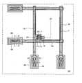
- FIG. 1is a schematic plan view of an LCD panel having a COG-type IC according to the related art
- FIG. 2is a cross sectional view along II-II of FIG. 1 according to the related art.
- a first substrate 10is attached and aligned with a second substrate 50 such that the attached first and second substrates 10 and 50 constitute an LCD panel L.P.
- the first substrate 10includes a plurality of gate and data pads (no shown) and IC chips 60 and 62 in electrical communication with the gate and data pads.
- the IC chips 60 and 62are disposed along peripheries of the first substrate 10 that are not overlapped by the second substrate 50 .
- the first substrate 10includes a plurality of gate and data lines that perpendicularly cross one another to define a plurality of pixel regions, wherein the gate pad is disposed at each end of the gate lines, and the data pad is placed at each one end of the data lines.
- the gate padsare located along the periphery where the gate driving IC chip 60 is placed such that the gate diving IC chip 60 is connected to the gate pads.
- the data padsare located along the periphery where the data driving IC chip 60 is placed such that the data driving IC chip 62 is connected to the data pads.
- a multi-layered flexible printed circuit board (FPCB) 70is connected to the first substrate 10 through an anisotropic conductive film 80 to supply the driving signals to the driving IC ships 60 and 62 .
- FIG. 3is a partially enlarged plan view of an array substrate according to the related art.
- an array substrate 10includes a plurality of gate lines 14 disposed along a transverse direction and a plurality of data lines 28 disposed along a longitudinal direction, wherein the plurality of gate lines 14 and the plurality of data lines 28 cross one another to define pixel regions P.
- Each of the gate lines 14 and each of the data lines 28include a gate pad 16 and a data pad 30 , respectively, disposed at ends of each of the gate lines 14 and at ends of each of the data lines 28 .
- a gate pad terminal 46is disposed over the gate pad 16
- a data pad terminal 48is disposed over the data pad 30 .
- a TFT Tis formed at each of the crossing portions of the gate lines 14 and the data lines 28 , and may include a gate electrode 12 , an active layer 20 , a source electrode 24 , and a drain electrode 26 .
- a pixel electrode 44may be disposed within the pixel region P defined by the gate and data lines 14 and 28 , wherein the pixel electrode 44 and the gate and data pads terminals 46 and 48 are formed of a transparent conductive material.
- FIG. 4is a cross sectional view along IV-IV of FIG. 3 according to the related art
- FIG. 5is a cross sectional view along V-V of FIG. 3 according to the related art
- FIG. 6is a cross sectional view along VI-VI of FIG. 3 according to the related art.
- a switching region S, a pixel region P, a gate pad region G, and a data pad region Dare defined on a substrate 10 , wherein the gate electrode 12 is formed on the substrate 10 within the switching region S.
- the gate line 14is also disposed on the substrate 10 , and the gate electrode 12 extends from the gate line 14 .
- the gate pad 16is formed on the substrate 10 within the gate pad region G, and is connected to the end of the gate line 14 (in FIG. 3 ).
- a gate insulating layer 18which is formed of an inorganic material, is formed on the substrate 10 covering the gate electrode 12 , the gate line 14 , and the gate pad 16 .
- an active later 20is formed on the gate insulating layer 18
- an ohmic contact layer 22is disposed on the active layer 20 .
- the active and ohmic contact layers 20 and 22are disposed over the gate electrode 12
- the source and drain electrodes 24 and 26are disposed over the active layer 20 and are in contact with the ohmic contact layer 22 , respectively.
- the data line 28is disposed on the gate insulating layer 18
- the data pad 30is also disposed on the gate insulating layer 18 within the data pad region D.
- the data pad 30is connected to the end of the data line 28 .
- the TFT T including the gate electrode 12 , the active layer 20 , the ohmic contact layer 22 , the source electrode 24 , and the drain electrode 26is formed over the substrate 10 within the switching region S, and the gate and data pads 16 and 30 are formed within the gate and data pad regions G and D, respectively.
- a first passivation layer 32 of an inorganic materialis formed along an entire surface of the substrate 10 to cover the TFT T and the gate and data pads 16 and 30 .
- a second passivation layer 34is disposed along an entire surface of the first passivation layer 32
- a third passivation layer 36is disposed along an entire surface of the second passivation layer 34 .
- the second passivation layer 34is an organic material
- the first and third passivation layers 32 and 36are an inorganic material.
- the organic material for the second passivation layer 34may be, for example, benzocyclobutene (BCB) or acrylic resin
- the inorganic material for the first and third passivation layers 32 and 36may be, for example, silicon nitride (SiN x ) or silicon oxide (SiO 2 ).
- the first passivation layer 32 of inorganic materialfunctions as a buffer layer to protect the active layer 20 from the passivation layer 34 formed of organic material. If the organic second passivation layer 36 contacts the active layer 20 , a trap potential that interrupts carrier movement within a channel region of the TFT T may occur along an interface between the active layer 20 and the second passivation layer, thereby deteriorating operational characteristics of the TFT T. Therefore, the inorganic first passivation layer 32 is interposed between the TFT T and the organic second passivation layer 34 .
- the organic material for the second passivation layer 34usually has a dielectric constant of less than 3, cross talk is prevented between the pixel electrode 44 and the lines 14 and 28 .
- the second passivation layer 34increases aperture ratio.
- the aperture ratiois raised according to an extension of the pixel electrode 44 . Accordingly, the third passivation layer 36 functions to interrupt light incident to the active layer 20 .
- the first, second, and third passivation layers 32 , 34 , and 36are simultaneously patterned to form first, second, and third contact holes H 1 , H 2 , and H 3 .
- the first contact hole H 1exposes a portion of the drain electrode 26
- the second contact hole H 2exposes a portion of the gate pad 16
- the third contact hole H 3exposes a portion of the data pad 30 .
- the second contact hole H 2penetrates the first, second, and third passivation layers 32 , 34 , and 36 and the gate insulating layer 18 , whereas the first and second contact holes H 1 and H 3 penetrate only the first, second, and third passivation layers 32 , 34 , and 36 .
- the pixel electrode 44is formed on the third passivation layer 36 to correspond to the pixel region P. Furthermore, when forming the pixel electrode 44 , the gate and data pad terminals 46 and 48 are formed within the gate and data pad regions G and D, respectively. Accordingly, the pixel electrode 44 contacts the drain electrode 26 through the first contact hole H 1 , the gate pad terminal 46 contacts the gate pad 16 through the second contact hole H 2 , and the data pad terminal 48 contacts the data pad 30 through the third contact hole H 3 .
- the organic passivation layeris necessary in order to obtain the high aperture ratio.
- the structurecauses some disadvantages within the gate and data pad regions G and D when installing the IC chips on the array substrate.
- FIG. 7is a cross sectional view along V-V of FIG. 3 of a gate pad region during application of an IC chip according to the related art.
- the first, second, and third passivation layers 32 , 34 and 36are simultaneously etched to form the second contact hole H 2 that exposes the portion of the gate pad 16 .
- abnormal etchingoccurs due to the inorganic first and third passivation layers 32 and 36 and the organic second passivation layer 34 having different etching selectivities.
- one of the organic and inorganic layersis over-etched during the patterning process such that the second hole H 2 may have uneven surfaces along sidewalls of the second hole H 2 . Accordingly, the gate pad terminal 46 may be damaged, thereby creating an electrical open circuit condition. In addition, the electrical open circuit condition will be created within the data pad region D.
- the IC chip 60when the IC chip 60 , having a bump 60 a , is attached to the gate pad terminal 46 during the COG process, the IC chip 60 is electrically isolated from the gate pad 16 .
- the bump 60 a of the IC chip 60is larger than the second contact hole H 2 , the bump 60 a is disposed on and in contact with the gate pad terminal 46 .
- the gate pad terminal 46since the gate pad terminal 46 is damaged within the second contact hole H 2 , the gate pad terminal 46 does not electrically connect the gate pad 16 to the bump 60 a of the IC chip 60 , and the IC chip 60 is placed into an electrically floating state with respect to the gate pad 16 .
- the IC chip 60can not supply the signals to the gate pad 16 .
- FIG. 8is a cross sectional view along V-V of FIG. 3 of another gate pad region during application of an IC chip according to the related art.
- the bump 60 a of the IC chip 60since the bump 60 a of the IC chip 60 has a relatively small size to fit within the second contact hole H 2 , the bump 60 a impacts the gate pad terminal 46 . Accordingly, the gate pad terminal 46 becomes detached from organic second passivation layer 34 and is damaged. Thus, the IC chip 60 is not electrically connected with the gate pad 16 .
- the IC chip 60 or the flexible printed circuit board (FPCB) 70(in FIG. 2 ) is removed from the array substrate and a re-work process for re-attaching the IC chip 60 to the gate pad terminal 46 is performed.
- the gate pad terminal 46may be damaged such that a subsequent re-work process may not be performed since the gate pad terminal 46 is damaged beyond repair.
- the present inventionis directed to a chip-on-glass (COG) array substrate of an LCD device and a method of fabricating a chip-on-glass (COG) array substrate of an LCD device that substantially obviates one or more of the problems due to limitations and disadvantages of the related art.
- An object of the present inventionis to provide an array substrate having pad structures that prevent damage.
- Another object of the present inventionis to provide a method of fabricating an array substrate having pad structures that prevent damage.
- Another object of the present inventionis to provide an array substrate having pad structures to afford stable attachment of IC chips.
- Another object of the present inventionis to provide a method of fabricating an array substrate having pad structures to afford stable attachment of IC chips.
- an array substrate device for a liquid crystal display deviceincludes a gate line disposed along a first direction on a substrate, a gate pad on the substrate and connected to a first end of the gate line, a gate insulating layer on the substrate covering the gate line and the gate pad, a data line disposed along a second direction over the gate insulating layer and crossing the gate line to define a pixel region, a data pad connected to a first end of the data line, a thin film transistor disposed at a crossing region of the gate and data lines, a first inorganic insulating layer formed on the substrate covering the thin film transistor, the data line, and the data pad, a first organic insulating layer along an entire surface of the first inorganic insulation layer except at portions corresponding to the gate and data pads, a transparent pixel electrode disposed over the first organic insulating layer and connected to the thin film transistor, and a transparent gate pad terminal and a data pad terminal
- a method of fabricating an array substrate device for a liquid crystal display deviceincludes forming a gate line and a gate pad on a substrate, the gate line disposed along a first direction and the gate pad is connected to a first end of the gate line, forming a gate insulating layer over the substrate to cover the gate line and the gate pad, forming a data line and a data pad over the gate insulating layer, the data line disposed along a second direction to cross the gate line to define a pixel region, and the data pad is connected to a first end of the data line, forming a thin film transistor at a crossing region of the gate and data lines, sequentially forming a first inorganic insulating layer and a first organic insulating layer over the substrate to cover the thin film transistor, the data line, and the data pad, patterning the first organic insulating layer to expose portions of the first inorganic insulating layer corresponding to the gate and data pads, forming a second inorganic insulating layer over the patterned first organic insul
- FIG. 1is a schematic plan view of an LCD panel having a COG-type IC according to the related art
- FIG. 2is a cross sectional view along II-II of FIG. 1 according to the related art
- FIG. 3is a partially enlarged plan view of an array substrate according to the related art
- FIG. 4is a cross sectional view along IV-IV of FIG. 3 according to the related art
- FIG. 5is a cross sectional view along V-V of FIG. 3 according to the related art
- FIG. 6is a cross sectional view along VI-VI of FIG. 3 according to the related art.
- FIG. 8is a cross sectional view along V-V of FIG. 3 of another gate pad region during application of an IC chip according to the related art
- FIG. 9is an enlarged plan view of an exemplary array substrate for an LCD device according to the present invention.
- FIGS. 10A-10Gare cross sectional views along IV-IV of FIG. 9 of an exemplary method of fabricating an array substrate according to the present invention.
- FIGS. 11A-11Gare cross sectional views along V-V of FIG. 9 of another exemplary method of fabricating an array substrate according to the present invention.
- FIGS. 12A-12Gare cross sectional views along V-V of FIG. 9 of another exemplary method of fabricating an array substrate according to the present invention.
- a first metal layermay be deposited onto a surface of a substrate 100 , and patterned to form a gate line 104 (in FIG. 9 ), a gate electrode 102 , and a gate pad 106 on the substrate 100 .
- the gate pad 106may be disposed at an end portion of the gate line 104 (In FIG. 9 ), and the gate electrode 102 may extend from the gate line.
- the first metal layermay be one of aluminum-based material(s), such as aluminum (Al) or an aluminum-alloy such as aluminum neodymium (AlNd), having low electrical resistance in order to prevent signal delay.
- the aluminum-based materialaluminum (Al), aluminum-alloy, or aluminum neodymium (AlNd)
- Alaluminum
- AlNdaluminum neodymium
- the gate line 104In FIG. 9
- a gate insulating layer 108may be formed on the substrate 100 to cover the gate line 104 (In FIG. 9 ), the gate electrode 102 , and the gate pad 106 .
- the gate insulating layer 108may fully cover the gate electrode 102 , the gate line 104 (in FIG. 9 ), and the gate pad 106 , and may include inorganic material(s), such as silicon nitride (SiN x ) and silicon oxide (SiO 2 ).
- an intrinsic amorphous silicon layersuch as a—Si:H
- a doped amorphous silicon layersuch as n + a—Si:H
- an active layer 110 and an ohmic contact layer 112may be sequentially deposited along an entire surface of the gate insulating layer 108 , and may be simultaneously patterned using a mask process to form an active layer 110 and an ohmic contact layer 112 .
- the ohmic contact layer 112may be located on the active layer 110 over the gate electrode 102 .
- a second metal layermay be formed on the gate insulating layer 108 to cover both the active layer 110 and the ohmic contact layer 112 .
- the second metal layermay include molybdenum (Mo), titanium (Ti), copper (Cu), tungsten (W), and/or chromium (Cr).
- Momolybdenum
- Tititanium
- Cucopper
- Wtungsten
- Crchromium
- the second metal layermay be patterned to form a source electrode 114 , a drain electrode 116 , a data line 118 , and a data pad 120 over the substrate 100 .
- the source electrode 114may extend from the data line 118 and may contact a first portion of the ohmic contact layer 112 .
- the drain electrode 116may be spaced apart from the source electrode 114 across the gate electrode 102 and may contact a second portion of the ohmic contact layer 112 .
- the data pad 120may be provided at an end portion of the data line 118 .
- portions of the second passivation layer 124may be removed by an etching process.
- the portions corresponding to the gate and data pads 106 and 120may be completely removed to expose the underlying first passivation layer 122 .
- the portion of the second passivation layer 124 within the pixel regionmay not be removed, the portions within the gate and data regions may be completely removed, as shown in FIGS. 11E and 12E .
- a third passivation layer 126may be formed along an entire surface of the substrate 100 to cover the patterned second passivation layer 124 .
- the third passivation layer 126may be, for example, silicon nitride (SiN x ) or silicon oxide (SiO 2 ), and may protect the channel region of the active layer 110 from light incident. Accordingly, if the incident light irradiates the channel region between the source and drain electrodes 114 and 116 , a photocurrent is generated within the active layer 110 and causes a leakage current in the TFT T.
- the first, second, and third passivation layers 122 , 124 , and 126may be simultaneously patterned to form a drain contact hole 128 , a gate pad contact hole 130 , and a data pad contact hole 132 . Accordingly, a portion of the gate insulating layer 108 underneath the gate pad contact hole 130 may also be removed to expose the gate pad 106 .
- the drain contact hole 128may penetrate through the first, second, and third passivation layers 122 , 124 , and 126 , and may expose a portion of the drain electrode 116 .
- the gate pad contact hole 130may penetrate through the gate insulating layer 108 and the first and third passivation layers 122 and 126 , thereby exposing a portion of the gate pad 106 .
- the data pad contact hole 132may penetrate through the first and third passivation layers 122 and 126 , thereby exposing a portion of the data pad 120 .
- a transparent conductive materialmay be deposited over the patterned third passivation layer 126 including the drain contact hole 128 , the gate pad contact hole 130 , and the data pad contact hole 132 . Then, the transparent conductive material may be patterned to form a pixel electrode 134 , a gate pad terminal 136 , and a data pad terminal 138 .
- the transparent conductive materialmay include one of indium tin oxide (ITO) and indium zinc oxide (IZO).
- the pixel electrode 134may contact the drain electrode 116 through the drain contact hole 128 , the gate pad terminal 136 may contact the gate pad 106 through the gate pad contact hole 130 , and the data pad terminal 138 may contact the data pad 120 through the data pad contact hole 132 .
- FIG. 13is a cross sectional view along V-V of FIG. 9 of an exemplary gate pad region during application of an IC chip according to the present invention.
- a gate pad regionmay not include an organic second passivation layer 134 , wherein layers formed on a gate pad 106 may only comprise inorganic material(s), such as silicon nitride (SiN x ) or silicon oxide (SiO 2 ).
- a gate insulating layer 108 and first and third passivation layers 122 and 126may be formed over a gate pad 106 , and may not have an etch selectivity difference since these layers are formed of the same material.
- a gate pad terminal 136may be stably and firmly attached to the gate pad 106 without creating any cracks or causing any damage to the gate pad 106 . Furthermore, when an IC chip 220 having a bump 220 a is applied to the gate pad 106 , the IC chip 220 may be in electrical communication with the gate pad 106 through the gate pad terminal 136 and the bump 220 a . Accordingly, since re-work processing is not required, manufacturing yield increases. Furthermore, an LCD device including the array substrate described above can display images having improved quality.
Landscapes
- Physics & Mathematics (AREA)
- Nonlinear Science (AREA)
- Mathematical Physics (AREA)
- Chemical & Material Sciences (AREA)
- Crystallography & Structural Chemistry (AREA)
- General Physics & Mathematics (AREA)
- Optics & Photonics (AREA)
- Engineering & Computer Science (AREA)
- Microelectronics & Electronic Packaging (AREA)
- Liquid Crystal (AREA)
- Devices For Indicating Variable Information By Combining Individual Elements (AREA)
Abstract
Description
- The present invention claims the benefit of Korean Patent Application No. P2003-0057793, filed in Korea on Aug. 21, 2003, which is hereby incorporated by reference.
- 1. Field of the Invention
- The present invention relates to a liquid crystal display (LCD) device, and more particularly, to an array substrate chip-on-glass (COG) type array substrate of an LCD device.
- 2. Discussion of the Related Art
- In general, an LCD device includes a liquid crystal panel having upper and lower substrates and a liquid crystal layer disposed between the upper and lower substrates, wherein peripheral portions of the upper and lower substrates are sealed together by a sealant to prevent leakage of the liquid crystal layer. The upper substrate, which is commonly referred to as a color filter substrate, includes a common electrode and color filters. The lower substrate, which is commonly referred to as an array substrate, includes gate lines arranged along a transverse direction and data lines arranged along a longitudinal direction perpendicular to the gate lines. In addition, a pixel electrode is formed within a pixel region of the lower substrate defined by crossing regions of the gate and data lines, and a thin film transistor (TFT) is formed to function as a switching element at the crossing regions of the gate and data lines in a matrix. The TFT includes a gate electrode, a source electrode, and a drain electrode, wherein the drain electrode contacts the pixel electrode via a drain contact hole. Accordingly, the gate lines transmit scanning signals to the gate electrode, and the data lines transmit data signals to the source electrode. Thus, the data signals change alignment of liquid crystal molecules of the liquid crystal layer according to the scanning signals in order to display images having various gray levels by the LCD device.
- Operation of the LCD device makes use of optical anisotropy and polarization properties of the liquid crystal molecules in order to generate desired images. For example, the liquid crystal molecules have specific alignments due to their specific characteristics that can be modified by an induced electric field. Accordingly, since the electric fields induced to the liquid crystal molecules can change the specific alignments of the liquid crystal molecules, incident light is refracted according to the specific alignments of the liquid crystal molecules due to the optical anisotropy of the liquid crystal molecules.
- Each of the upper and lower substrates have electrodes that are spaced apart and face into each other. Accordingly, when the electric field is induced to the liquid crystal material through the electrodes of each substrate, alignment directions of the liquid crystal molecules are changed in accordance with the applied voltage to display images. By controlling the induced voltage, the LCD device provides various light transmittances to display images.
- Among the different types of LCD devices, active matrix LCD (AM-LCD) devices having TFTs and pixel electrodes arranged in a matrix configuration produce high resolution images, and produce superior moving images. In the AM-LCD devices, driver integrated circuits (IC) apply signals to each electrode through a plurality of conductive lines disposed on the lower substrate, and may be mounted using various methods, such as chip on board (COB), tape carrier package (TCP), and chip on glass (COG) methods.
- The COB method is commonly adopted for segment-type LCD devices, or for LCD panels having low resolution. Since the segment-type LCD devices or the low resolution LCD panels use small numbers of leads, the driver ICs thereof also have small numbers of leads. Accordingly, the driver ICs thereof are first installed on a printed circuit board (PCB) having a plurality of leads, and the leads of the PCB are connected with the LCD panel via one of the various methods described above. However, as resolution of LCD devices has increased, an increased number of leads are required for the driver ICs. Thus, when the number of leads increases, it is difficult to install the driver ICs on the PCB.
- According to the TCP method, the driver ICs are installed onto a polymer film. Thus, the TCP method is commonly used for LCD devices that require small, thin, light weight packages, such as mobile phones.
- According to the COG method, the driver ICs are directly installed onto the LCD panel without the use of an interposing PCB. Thus, electrical connections between the driver ICs and the LCD panel is miniaturized, wherein a pitch between adjacent leads of the driver ICs is relatively small. The COG method employs a multi-layered flexible printed circuit board (FPCB) instead of the PCB, wherein the multi-layered FPCB contacts the LCD panel via an anisotropic conductive film (ACF) and transmits input signals to the driver ICs.
- Although the COG method has advantages, such as low cost and high stability, since a pad of the LCD panel requires an additional area to install the driver ICs, the LCD panel must be enlarged. In addition, by using the COG method, it is difficult to remove and repair defective ones of the driver ICs or to repair terminal lines of the LCD panel.
FIG. 1 is a schematic plan view of an LCD panel having a COG-type IC according to the related art, andFIG. 2 is a cross sectional view along II-II ofFIG. 1 according to the related art. InFIGS. 1 and 2 , afirst substrate 10 is attached and aligned with asecond substrate 50 such that the attached first andsecond substrates first substrate 10 includes a plurality of gate and data pads (no shown) andIC chips IC chips first substrate 10 that are not overlapped by thesecond substrate 50. Although not shown, thefirst substrate 10 includes a plurality of gate and data lines that perpendicularly cross one another to define a plurality of pixel regions, wherein the gate pad is disposed at each end of the gate lines, and the data pad is placed at each one end of the data lines. Specifically, the gate pads are located along the periphery where the gate drivingIC chip 60 is placed such that the gatediving IC chip 60 is connected to the gate pads. Accordingly, the data pads are located along the periphery where the data drivingIC chip 60 is placed such that the data drivingIC chip 62 is connected to the data pads. InFIG. 2 , a multi-layered flexible printed circuit board (FPCB)70 is connected to thefirst substrate 10 through an anisotropicconductive film 80 to supply the driving signals to the drivingIC ships FIG. 3 is a partially enlarged plan view of an array substrate according to the related art. InFIG. 3 , anarray substrate 10 includes a plurality ofgate lines 14 disposed along a transverse direction and a plurality ofdata lines 28 disposed along a longitudinal direction, wherein the plurality ofgate lines 14 and the plurality ofdata lines 28 cross one another to define pixel regions P. Each of thegate lines 14 and each of thedata lines 28 include agate pad 16 and adata pad 30, respectively, disposed at ends of each of thegate lines 14 and at ends of each of thedata lines 28. In addition, agate pad terminal 46 is disposed over thegate pad 16, and adata pad terminal 48 is disposed over thedata pad 30. A TFT T is formed at each of the crossing portions of thegate lines 14 and thedata lines 28, and may include agate electrode 12, anactive layer 20, asource electrode 24, and adrain electrode 26. Apixel electrode 44 may be disposed within the pixel region P defined by the gate anddata lines pixel electrode 44 and the gate anddata pads terminals FIGS. 4-6 .FIG. 4 is a cross sectional view along IV-IV ofFIG. 3 according to the related art,FIG. 5 is a cross sectional view along V-V ofFIG. 3 according to the related art, andFIG. 6 is a cross sectional view along VI-VI ofFIG. 3 according to the related art. InFIGS. 4-6 , a switching region S, a pixel region P, a gate pad region G, and a data pad region D are defined on asubstrate 10, wherein thegate electrode 12 is formed on thesubstrate 10 within the switching region S. As shown inFIG. 3 , thegate line 14 is also disposed on thesubstrate 10, and thegate electrode 12 extends from thegate line 14. InFIG. 5 , thegate pad 16 is formed on thesubstrate 10 within the gate pad region G, and is connected to the end of the gate line14 (inFIG. 3 ). Then, agate insulating layer 18, which is formed of an inorganic material, is formed on thesubstrate 10 covering thegate electrode 12, thegate line 14, and thegate pad 16. Next, an active later20 is formed on thegate insulating layer 18, and anohmic contact layer 22 is disposed on theactive layer 20. Specifically, the active andohmic contact layers gate electrode 12, the source anddrain electrodes active layer 20 and are in contact with theohmic contact layer 22, respectively. Thedata line 28 is disposed on thegate insulating layer 18, and thedata pad 30 is also disposed on thegate insulating layer 18 within the data pad region D.- In
FIG. 3 , thedata pad 30 is connected to the end of thedata line 28. Accordingly, the TFT T including thegate electrode 12, theactive layer 20, theohmic contact layer 22, thesource electrode 24, and thedrain electrode 26 is formed over thesubstrate 10 within the switching region S, and the gate anddata pads - Then, a
first passivation layer 32 of an inorganic material is formed along an entire surface of thesubstrate 10 to cover the TFT T and the gate anddata pads second passivation layer 34 is disposed along an entire surface of thefirst passivation layer 32, and athird passivation layer 36 is disposed along an entire surface of thesecond passivation layer 34. Thesecond passivation layer 34 is an organic material, while the first andthird passivation layers second passivation layer 34 may be, for example, benzocyclobutene (BCB) or acrylic resin, and the inorganic material for the first andthird passivation layers - The
first passivation layer 32 of inorganic material functions as a buffer layer to protect theactive layer 20 from thepassivation layer 34 formed of organic material. If the organicsecond passivation layer 36 contacts theactive layer 20, a trap potential that interrupts carrier movement within a channel region of the TFT T may occur along an interface between theactive layer 20 and the second passivation layer, thereby deteriorating operational characteristics of the TFT T. Therefore, the inorganicfirst passivation layer 32 is interposed between the TFT T and the organicsecond passivation layer 34. - Since the organic material for the
second passivation layer 34 usually has a dielectric constant of less than 3, cross talk is prevented between thepixel electrode 44 and thelines pixel electrode 44 extends over the gate anddata lines second passivation layer 34 increases aperture ratio. When the organic material is utilized for the passivation layer, the aperture ratio is raised according to an extension of thepixel electrode 44. Accordingly, thethird passivation layer 36 functions to interrupt light incident to theactive layer 20. - After forming the
third passivation layer 36 and before forming thepixel electrode 44, the first, second, and third passivation layers32,34, and36 are simultaneously patterned to form first, second, and third contact holes H1, H2, and H3. The first contact hole H1 exposes a portion of thedrain electrode 26, the second contact hole H2 exposes a portion of thegate pad 16, and the third contact hole H3 exposes a portion of thedata pad 30. The second contact hole H2 penetrates the first, second, and third passivation layers32,34, and36 and thegate insulating layer 18, whereas the first and second contact holes H1 and H3 penetrate only the first, second, and third passivation layers32,34, and36. - After patterning the first, second, and third passivation layers32,34, and36, the
pixel electrode 44 is formed on thethird passivation layer 36 to correspond to the pixel region P. Furthermore, when forming thepixel electrode 44, the gate anddata pad terminals pixel electrode 44 contacts thedrain electrode 26 through the first contact hole H1, thegate pad terminal 46 contacts thegate pad 16 through the second contact hole H2, and thedata pad terminal 48 contacts thedata pad 30 through the third contact hole H3. - In
FIGS. 3-6 , the organic passivation layer is necessary in order to obtain the high aperture ratio. However, the structure causes some disadvantages within the gate and data pad regions G and D when installing the IC chips on the array substrate. FIG. 7 is a cross sectional view along V-V ofFIG. 3 of a gate pad region during application of an IC chip according to the related art. InFIG. 7 , the first, second, and third passivation layers32,34 and36 are simultaneously etched to form the second contact hole H2 that exposes the portion of thegate pad 16. However, during simultaneous etching of the first, second, and third passivation layers32,34, and36, abnormal etching occurs due to the inorganic first and third passivation layers32 and36 and the organicsecond passivation layer 34 having different etching selectivities. For example, one of the organic and inorganic layers is over-etched during the patterning process such that the second hole H2 may have uneven surfaces along sidewalls of the second hole H2. Accordingly, thegate pad terminal 46 may be damaged, thereby creating an electrical open circuit condition. In addition, the electrical open circuit condition will be created within the data pad region D.- As a result, when the
IC chip 60, having abump 60a, is attached to thegate pad terminal 46 during the COG process, theIC chip 60 is electrically isolated from thegate pad 16. When thebump 60aof theIC chip 60 is larger than the second contact hole H2, thebump 60ais disposed on and in contact with thegate pad terminal 46. However, since thegate pad terminal 46 is damaged within the second contact hole H2, thegate pad terminal 46 does not electrically connect thegate pad 16 to thebump 60aof theIC chip 60, and theIC chip 60 is placed into an electrically floating state with respect to thegate pad 16. Thus, theIC chip 60 can not supply the signals to thegate pad 16. FIG. 8 is a cross sectional view along V-V ofFIG. 3 of another gate pad region during application of an IC chip according to the related art. InFIG. 8 , since thebump 60aof theIC chip 60 has a relatively small size to fit within the second contact hole H2, thebump 60aimpacts thegate pad terminal 46. Accordingly, thegate pad terminal 46 becomes detached from organicsecond passivation layer 34 and is damaged. Thus, theIC chip 60 is not electrically connected with thegate pad 16.- When the damage is created to the
gate pad terminal 46, theIC chip 60 or the flexible printed circuit board (FPCB)70 (inFIG. 2 ) is removed from the array substrate and a re-work process for re-attaching theIC chip 60 to thegate pad terminal 46 is performed. However, when removing theIC chip 60 or the FPCB70 (inFIG. 2 ), thegate pad terminal 46 may be damaged such that a subsequent re-work process may not be performed since thegate pad terminal 46 is damaged beyond repair. - Accordingly, the present invention is directed to a chip-on-glass (COG) array substrate of an LCD device and a method of fabricating a chip-on-glass (COG) array substrate of an LCD device that substantially obviates one or more of the problems due to limitations and disadvantages of the related art.
- An object of the present invention is to provide an array substrate having pad structures that prevent damage.
- Another object of the present invention is to provide a method of fabricating an array substrate having pad structures that prevent damage.
- Another object of the present invention is to provide an array substrate having pad structures to afford stable attachment of IC chips.
- Another object of the present invention is to provide a method of fabricating an array substrate having pad structures to afford stable attachment of IC chips.
- Additional features and advantages of the invention will be set forth in the description which follows, and in part will be apparent from the description, or may be learned by practice of the invention. The objectives and other advantages of the invention will be realized and attained by the structure particularly pointed out in the written description and claims hereof as well as the appended drawings.
- To achieve these and other advantages and in accordance with the purpose of the present invention, as embodied and broadly described, an array substrate device for a liquid crystal display device includes a gate line disposed along a first direction on a substrate, a gate pad on the substrate and connected to a first end of the gate line, a gate insulating layer on the substrate covering the gate line and the gate pad, a data line disposed along a second direction over the gate insulating layer and crossing the gate line to define a pixel region, a data pad connected to a first end of the data line, a thin film transistor disposed at a crossing region of the gate and data lines, a first inorganic insulating layer formed on the substrate covering the thin film transistor, the data line, and the data pad, a first organic insulating layer along an entire surface of the first inorganic insulation layer except at portions corresponding to the gate and data pads, a transparent pixel electrode disposed over the first organic insulating layer and connected to the thin film transistor, and a transparent gate pad terminal and a data pad terminal disposed over the first organic insulating layer and connected to the gate and data pads, respectively.
- In another aspect, A method of fabricating an array substrate device for a liquid crystal display device includes forming a gate line and a gate pad on a substrate, the gate line disposed along a first direction and the gate pad is connected to a first end of the gate line, forming a gate insulating layer over the substrate to cover the gate line and the gate pad, forming a data line and a data pad over the gate insulating layer, the data line disposed along a second direction to cross the gate line to define a pixel region, and the data pad is connected to a first end of the data line, forming a thin film transistor at a crossing region of the gate and data lines, sequentially forming a first inorganic insulating layer and a first organic insulating layer over the substrate to cover the thin film transistor, the data line, and the data pad, patterning the first organic insulating layer to expose portions of the first inorganic insulating layer corresponding to the gate and data pads, forming a second inorganic insulating layer over the patterned first organic insulating layer and over the exposed portions of the first organic insulating layer, simultaneously patterning the second inorganic insulating layer, the first organic insulating layer, and the first inorganic insulating layer to form first, second, and third contact holes, and forming a transparent pixel electrode, and a transparent gate pad terminal, and a data pad terminal over the second inorganic insulating layer, wherein the pixel electrode contacts a portion of the thin film transistor through the first contact hole, and the gate pad terminal and data pad terminal contact the gate and data pads through the second and third contact holes, respectively.
- It is to be understood that both the foregoing general description and the following detailed description are exemplary and explanatory and are intended to provide further explanation of the invention as claimed.
- The accompanying drawings, which are included to provide a further understanding of the invention and are incorporated in and constitute a part of this specification, illustrate embodiments of the invention and together with the description serve to explain the principles of the invention. In the drawings:
FIG. 1 is a schematic plan view of an LCD panel having a COG-type IC according to the related art;FIG. 2 is a cross sectional view along II-II ofFIG. 1 according to the related art;FIG. 3 is a partially enlarged plan view of an array substrate according to the related art;FIG. 4 is a cross sectional view along IV-IV ofFIG. 3 according to the related art;FIG. 5 is a cross sectional view along V-V ofFIG. 3 according to the related art;FIG. 6 is a cross sectional view along VI-VI ofFIG. 3 according to the related art;FIG. 7 is a cross sectional view along V-V ofFIG. 3 of a gate pad region during application of an IC chip according to the related art;FIG. 8 is a cross sectional view along V-V ofFIG. 3 of another gate pad region during application of an IC chip according to the related art;FIG. 9 is an enlarged plan view of an exemplary array substrate for an LCD device according to the present invention;FIGS. 10A-10G are cross sectional views along IV-IV ofFIG. 9 of an exemplary method of fabricating an array substrate according to the present invention;FIGS. 11A-11G are cross sectional views along V-V ofFIG. 9 of another exemplary method of fabricating an array substrate according to the present invention;FIGS. 12A-12G are cross sectional views along V-V ofFIG. 9 of another exemplary method of fabricating an array substrate according to the present invention; andFIG. 13 is a cross sectional view along V-V ofFIG. 9 of an exemplary gate pad region during application of an IC chip according to the present invention.- Reference will now be made in detail to preferred embodiments, examples of which are illustrated in the accompanying drawings.
FIG. 9 is an enlarged plan view of an exemplary array substrate for an LCD device according to the present invention,FIGS. 10A-10G are cross sectional views along IV-IV ofFIG. 9 of an exemplary method of fabricating an array substrate according to the present invention,FIGS. 11A-11G are cross sectional views along V-V ofFIG. 9 of another exemplary method of an array substrate according to the present invention,FIGS. 12A-12G are cross sectional views along V-V ofFIG. 9 of another exemplary method of fabricating an array substrate according to the present invention, andFIG. 13 is a cross sectional view along V-V ofFIG. 9 of an exemplary gate pad region during application of an IC chip according to the present invention.- In
FIGS. 10A, 11A , and12A, a first metal layer may be deposited onto a surface of asubstrate 100, and patterned to form a gate line104 (inFIG. 9 ), agate electrode 102, and agate pad 106 on thesubstrate 100. Thegate pad 106 may be disposed at an end portion of the gate line104 (InFIG. 9 ), and thegate electrode 102 may extend from the gate line. The first metal layer may be one of aluminum-based material(s), such as aluminum (Al) or an aluminum-alloy such as aluminum neodymium (AlNd), having low electrical resistance in order to prevent signal delay. Although the aluminum-based material, aluminum (Al), aluminum-alloy, or aluminum neodymium (AlNd), may have low electrical resistance, they are chemically weak against developer and etchant materials used to fabricating the array substrate. For example, although aluminum in the gate line reduces an RC delay due to its low resistance, aluminum is sensitive to acidity and susceptible to developing hillocks during high temperature fabrication processes or patterning processes, thereby creating line defects. Accordingly, chromium (Cr) or molybdenum (Mo) may be additionally formed on the first metal layer to protect the aluminum-based first metal layer from the developer and etchant materials. Thus, the gate line104 (InFIG. 9 ), thegate electrode 102, and thegate pad 106 may have a double-layered structure to include at least one of chromium (Cr) or molybdenum (Mo). - Then, a
gate insulating layer 108 may be formed on thesubstrate 100 to cover the gate line104 (InFIG. 9 ), thegate electrode 102, and thegate pad 106. Thegate insulating layer 108 may fully cover thegate electrode 102, the gate line104 (inFIG. 9 ), and thegate pad 106, and may include inorganic material(s), such as silicon nitride (SiNx) and silicon oxide (SiO2). - In
FIGS. 10B, 11B , and12B, an intrinsic amorphous silicon layer, such as a—Si:H, and a doped amorphous silicon layer, such as n+a—Si:H, may be sequentially deposited along an entire surface of thegate insulating layer 108, and may be simultaneously patterned using a mask process to form anactive layer 110 and anohmic contact layer 112. For example, theohmic contact layer 112 may be located on theactive layer 110 over thegate electrode 102. - In
FIGS. 10C, 11C , and12C, a second metal layer may be formed on thegate insulating layer 108 to cover both theactive layer 110 and theohmic contact layer 112. For example, the second metal layer may include molybdenum (Mo), titanium (Ti), copper (Cu), tungsten (W), and/or chromium (Cr). Then, the second metal layer may be patterned to form asource electrode 114, adrain electrode 116, adata line 118, and adata pad 120 over thesubstrate 100. Thesource electrode 114 may extend from thedata line 118 and may contact a first portion of theohmic contact layer 112. Thedrain electrode 116 may be spaced apart from thesource electrode 114 across thegate electrode 102 and may contact a second portion of theohmic contact layer 112. In addition, thedata pad 120 may be provided at an end portion of thedata line 118. After forming the source and drainelectrodes ohmic contact layer 112 located between the source and drainelectrodes active layer 110. Accordingly, formation of the channel region may include using the source and drainelectrodes - In
FIGS. 10D, 11D , and12D, first and second passivation layers122 and114 may be sequentially formed along an entire surface of thesubstrate 100 to cover the source and drainelectrodes data line 118, and thedata pad 120. For example, thefirst passivation layer 122 may be an inorganic material, such as silicon nitride (SiNx) or silicon oxide (SiO2), and thesecond passivation layer 124 may be an organic material, such as benzocyclobutene (BCB) or an acrylic resin. Since thefirst passivation layer 122 of inorganic material may be interposed between the exposed portion of theactive layer 110 and the organicsecond passivation layer 124, a trap potential for trapping carriers within the channel region may be minimized. - In
FIGS. 10E, 11E , and12E, portions of thesecond passivation layer 124 may be removed by an etching process. For example, the portions corresponding to the gate anddata pads first passivation layer 122. In addition, although the portion of thesecond passivation layer 124 within the pixel region may not be removed, the portions within the gate and data regions may be completely removed, as shown inFIGS. 11E and 12E . - In
FIGS. 10F, 11F , and12F, athird passivation layer 126 may be formed along an entire surface of thesubstrate 100 to cover the patternedsecond passivation layer 124. Thethird passivation layer 126 may be, for example, silicon nitride (SiNx) or silicon oxide (SiO2), and may protect the channel region of theactive layer 110 from light incident. Accordingly, if the incident light irradiates the channel region between the source and drainelectrodes active layer 110 and causes a leakage current in the TFT T. - Next, the first, second, and third passivation layers122,124, and126 may be simultaneously patterned to form a
drain contact hole 128, a gatepad contact hole 130, and a datapad contact hole 132. Accordingly, a portion of thegate insulating layer 108 underneath the gatepad contact hole 130 may also be removed to expose thegate pad 106. Thedrain contact hole 128 may penetrate through the first, second, and third passivation layers122,124, and126, and may expose a portion of thedrain electrode 116. The gatepad contact hole 130 may penetrate through thegate insulating layer 108 and the first and third passivation layers122 and126, thereby exposing a portion of thegate pad 106. The datapad contact hole 132 may penetrate through the first and third passivation layers122 and126, thereby exposing a portion of thedata pad 120. - In
FIGS. 10G, 11G , and12G, a transparent conductive material may be deposited over the patternedthird passivation layer 126 including thedrain contact hole 128, the gatepad contact hole 130, and the datapad contact hole 132. Then, the transparent conductive material may be patterned to form apixel electrode 134, agate pad terminal 136, and adata pad terminal 138. The transparent conductive material may include one of indium tin oxide (ITO) and indium zinc oxide (IZO). Thepixel electrode 134 may contact thedrain electrode 116 through thedrain contact hole 128, thegate pad terminal 136 may contact thegate pad 106 through the gatepad contact hole 130, and thedata pad terminal 138 may contact thedata pad 120 through the datapad contact hole 132. FIG. 13 is a cross sectional view along V-V ofFIG. 9 of an exemplary gate pad region during application of an IC chip according to the present invention. InFIG. 13 , a gate pad region may not include an organicsecond passivation layer 134, wherein layers formed on agate pad 106 may only comprise inorganic material(s), such as silicon nitride (SiNx) or silicon oxide (SiO2). For example, agate insulating layer 108 and first and third passivation layers122 and126 may be formed over agate pad 106, and may not have an etch selectivity difference since these layers are formed of the same material. Accordingly, agate pad terminal 136 may be stably and firmly attached to thegate pad 106 without creating any cracks or causing any damage to thegate pad 106. Furthermore, when anIC chip 220 having abump 220ais applied to thegate pad 106, theIC chip 220 may be in electrical communication with thegate pad 106 through thegate pad terminal 136 and thebump 220a. Accordingly, since re-work processing is not required, manufacturing yield increases. Furthermore, an LCD device including the array substrate described above can display images having improved quality.- It will be apparent to those skilled in the art that various modifications and variations can be made in the chip-on-glass (COG) array substrate of an LCD device and a method of fabricating a chip-on-glass (COG) array substrate of an LCD device of the present invention without departing from the spirit or scope of the invention. Thus, it is intended that the present invention cover the modifications and variations of this invention provided they come within the scope of the appended claims and their equivalents.
Claims (14)
Priority Applications (1)
| Application Number | Priority Date | Filing Date | Title |
|---|---|---|---|
| US11/349,210US7522225B2 (en) | 2003-08-21 | 2006-02-08 | Chip-on-glass array substrate of liquid crystal display device and method of fabricating the same |
Applications Claiming Priority (2)
| Application Number | Priority Date | Filing Date | Title |
|---|---|---|---|
| KR1020030057793AKR101034181B1 (en) | 2003-08-21 | 2003-08-21 | Manufacturing method of array substrate for liquid crystal display device |
| KR2003-0057793 | 2003-08-21 |
Related Child Applications (1)
| Application Number | Title | Priority Date | Filing Date |
|---|---|---|---|
| US11/349,210DivisionUS7522225B2 (en) | 2003-08-21 | 2006-02-08 | Chip-on-glass array substrate of liquid crystal display device and method of fabricating the same |
Publications (2)
| Publication Number | Publication Date |
|---|---|
| US20050041191A1true US20050041191A1 (en) | 2005-02-24 |
| US7053972B2 US7053972B2 (en) | 2006-05-30 |
Family
ID=36583357
Family Applications (2)
| Application Number | Title | Priority Date | Filing Date |
|---|---|---|---|
| US10/872,417Expired - LifetimeUS7053972B2 (en) | 2003-08-21 | 2004-06-22 | Chip-on-glass array substrate of liquid crystal display device and method of fabricating the same |
| US11/349,210Expired - LifetimeUS7522225B2 (en) | 2003-08-21 | 2006-02-08 | Chip-on-glass array substrate of liquid crystal display device and method of fabricating the same |
Family Applications After (1)
| Application Number | Title | Priority Date | Filing Date |
|---|---|---|---|
| US11/349,210Expired - LifetimeUS7522225B2 (en) | 2003-08-21 | 2006-02-08 | Chip-on-glass array substrate of liquid crystal display device and method of fabricating the same |
Country Status (2)
| Country | Link |
|---|---|
| US (2) | US7053972B2 (en) |
| KR (1) | KR101034181B1 (en) |
Cited By (13)
| Publication number | Priority date | Publication date | Assignee | Title |
|---|---|---|---|---|
| US20040263770A1 (en)* | 2003-06-24 | 2004-12-30 | Park Sung Il | Liquid crystal display device |
| US20070268442A1 (en)* | 2006-05-19 | 2007-11-22 | Samsung Electronics Co., Ltd. | Display substrate and method of manufacturing the same and liquid crystal display apparatus having the same |
| US20080049171A1 (en)* | 2006-07-14 | 2008-02-28 | Hiroyuki Takahashi | Display Device |
| US20080246133A1 (en)* | 2007-04-05 | 2008-10-09 | Micron Technology, Inc. | Flip-chip image sensor packages and methods of fabricating the same |
| US20090135103A1 (en)* | 2007-11-27 | 2009-05-28 | Changnam Kim | Organic light emitting device |
| US20090230395A1 (en)* | 2008-03-17 | 2009-09-17 | Jin-Suk Lee | Thin film transistor substrate and method for manufacturing the same |
| US20100149141A1 (en)* | 2008-12-17 | 2010-06-17 | Samsung Electronics Co., Ltd | Wiring of a display |
| US20140204300A1 (en)* | 2013-01-23 | 2014-07-24 | Samsung Display Co., Ltd. | Display device and manufacturing method thereof |
| US20160103378A1 (en)* | 2014-10-09 | 2016-04-14 | Mitsubishi Electric Corporation | Array substrate and liquid crystal display panel including the same |
| KR20160094582A (en)* | 2015-01-30 | 2016-08-10 | 엘지디스플레이 주식회사 | Liquid crystal display device and method for manufacturing the same |
| JP2018032034A (en)* | 2012-07-20 | 2018-03-01 | 株式会社半導体エネルギー研究所 | Display device |
| WO2022217599A1 (en)* | 2021-04-16 | 2022-10-20 | 京东方科技集团股份有限公司 | Array substrate, manufacturing method for array substrate, and display device |
| US11764229B2 (en) | 2020-11-20 | 2023-09-19 | Au Optronics Corporation | Pixel array substrate |
Families Citing this family (9)
| Publication number | Priority date | Publication date | Assignee | Title |
|---|---|---|---|---|
| KR100686345B1 (en)* | 2004-10-27 | 2007-02-22 | 삼성에스디아이 주식회사 | Flat panel display device and manufacturing method |
| KR101119196B1 (en)* | 2005-02-16 | 2012-03-22 | 삼성전자주식회사 | Display apparatus and method of fabricating the same |
| KR101623224B1 (en)* | 2008-09-12 | 2016-05-20 | 가부시키가이샤 한도오따이 에네루기 켄큐쇼 | Semiconductor device and method for manufacturing the same |
| KR100959284B1 (en)* | 2009-05-08 | 2010-05-26 | 삼성전자주식회사 | Display apparatus having display driving unit on the lower part |
| KR102246127B1 (en) | 2009-10-08 | 2021-04-29 | 가부시키가이샤 한도오따이 에네루기 켄큐쇼 | Semiconductor device |
| CN102709241A (en)* | 2012-05-11 | 2012-10-03 | 北京京东方光电科技有限公司 | Thin film transistor array substrate and preparation method and display device |
| CN102751240B (en)* | 2012-05-18 | 2015-03-11 | 京东方科技集团股份有限公司 | Thin film transistor array substrate, manufacturing method thereof, display panel and display device |
| JP6072522B2 (en)* | 2012-11-29 | 2017-02-01 | 三菱電機株式会社 | Liquid crystal display panel and manufacturing method thereof |
| KR102855117B1 (en) | 2021-06-03 | 2025-09-05 | 삼성디스플레이 주식회사 | Display device and method of manufacturing the same |
Citations (10)
| Publication number | Priority date | Publication date | Assignee | Title |
|---|---|---|---|---|
| US6055034A (en)* | 1996-06-25 | 2000-04-25 | Semiconductor Energy Laboratory Co., Ltd. | Liquid crystal display panel |
| US6115097A (en)* | 1996-05-16 | 2000-09-05 | Semiconductor Energy Laboratory Co., Ltd | Liquid crystal device with light blocking sealing member and light blocking electrode over two interlayer insulating films |
| US6288764B1 (en)* | 1996-06-25 | 2001-09-11 | Semiconductor Energy Laboratory Co., Ltd. | Display device or electronic device having liquid crystal display panel |
| US20010046016A1 (en)* | 1998-12-31 | 2001-11-29 | Woon-Yong Park | Thin film transistor array panels for a liquid crystal display and a method for manufacturing the same |
| US6373546B1 (en)* | 1997-03-03 | 2002-04-16 | Lg Philips Lcd Co., Ltd. | Structure of a liquid crystal display and the method of manufacturing the same |
| US20030038901A1 (en)* | 1998-10-21 | 2003-02-27 | Bum-Kee Baek | Method for manufacturing a thin film transistor array panel |
| US20040125293A1 (en)* | 2002-10-14 | 2004-07-01 | Jia-Shyong Cheng | Integrated color filter and fabricating method thereof |
| US20050179829A1 (en)* | 2002-04-15 | 2005-08-18 | Samsung Sdi Co., Ltd. | Flat panel display with black matrix and method of fabricating thereof |
| US6943859B2 (en)* | 2000-02-19 | 2005-09-13 | Lg.Philips Lcd Co., Ltd. | Liquid crystal display device and its fabricating method |
| US6952251B2 (en)* | 2001-08-30 | 2005-10-04 | Lg. Philips Lcd Co., Ltd. | Method for forming data lines of a liquid crystal display device |
Family Cites Families (1)
| Publication number | Priority date | Publication date | Assignee | Title |
|---|---|---|---|---|
| KR100255592B1 (en)* | 1997-03-19 | 2000-05-01 | 구본준 | Liquid crystal display device and its manufacturing method |
- 2003
- 2003-08-21KRKR1020030057793Apatent/KR101034181B1/ennot_activeExpired - Lifetime
- 2004
- 2004-06-22USUS10/872,417patent/US7053972B2/ennot_activeExpired - Lifetime
- 2006
- 2006-02-08USUS11/349,210patent/US7522225B2/ennot_activeExpired - Lifetime
Patent Citations (13)
| Publication number | Priority date | Publication date | Assignee | Title |
|---|---|---|---|---|
| US6115097A (en)* | 1996-05-16 | 2000-09-05 | Semiconductor Energy Laboratory Co., Ltd | Liquid crystal device with light blocking sealing member and light blocking electrode over two interlayer insulating films |
| US6577372B2 (en)* | 1996-06-25 | 2003-06-10 | Semiconductor Energy Laboratory Co., Ltd. | Electronic device having liquid crystal display device |
| US6288764B1 (en)* | 1996-06-25 | 2001-09-11 | Semiconductor Energy Laboratory Co., Ltd. | Display device or electronic device having liquid crystal display panel |
| US20040141140A1 (en)* | 1996-06-25 | 2004-07-22 | Semiconductor Energy Laboratory Co., Ltd., A Japan Corporation | Electronic device having liquid crystal display device |
| US6404479B2 (en)* | 1996-06-25 | 2002-06-11 | Semiconductor Energy Laboratory Co., Ltd. | Active matrix lcd comprising a sealing layer with a region overlapping an insulating film formed over another insulating film, and a region where said insulating film is not formed over said another insulating film |
| US6055034A (en)* | 1996-06-25 | 2000-04-25 | Semiconductor Energy Laboratory Co., Ltd. | Liquid crystal display panel |
| US6373546B1 (en)* | 1997-03-03 | 2002-04-16 | Lg Philips Lcd Co., Ltd. | Structure of a liquid crystal display and the method of manufacturing the same |
| US20030038901A1 (en)* | 1998-10-21 | 2003-02-27 | Bum-Kee Baek | Method for manufacturing a thin film transistor array panel |
| US20010046016A1 (en)* | 1998-12-31 | 2001-11-29 | Woon-Yong Park | Thin film transistor array panels for a liquid crystal display and a method for manufacturing the same |
| US6943859B2 (en)* | 2000-02-19 | 2005-09-13 | Lg.Philips Lcd Co., Ltd. | Liquid crystal display device and its fabricating method |
| US6952251B2 (en)* | 2001-08-30 | 2005-10-04 | Lg. Philips Lcd Co., Ltd. | Method for forming data lines of a liquid crystal display device |
| US20050179829A1 (en)* | 2002-04-15 | 2005-08-18 | Samsung Sdi Co., Ltd. | Flat panel display with black matrix and method of fabricating thereof |
| US20040125293A1 (en)* | 2002-10-14 | 2004-07-01 | Jia-Shyong Cheng | Integrated color filter and fabricating method thereof |
Cited By (36)
| Publication number | Priority date | Publication date | Assignee | Title |
|---|---|---|---|---|
| US20040263770A1 (en)* | 2003-06-24 | 2004-12-30 | Park Sung Il | Liquid crystal display device |
| US7256861B2 (en)* | 2003-06-24 | 2007-08-14 | Lg.Philips Lcd Co., Ltd. | Liquid crystal display device |
| US20070268442A1 (en)* | 2006-05-19 | 2007-11-22 | Samsung Electronics Co., Ltd. | Display substrate and method of manufacturing the same and liquid crystal display apparatus having the same |
| US20080049171A1 (en)* | 2006-07-14 | 2008-02-28 | Hiroyuki Takahashi | Display Device |
| US7965368B2 (en)* | 2006-07-14 | 2011-06-21 | Hitachi Displays, Ltd. | Display device comprising a semiconductor chip including a first terminal which overlaps a first and second line, the first terminal connected to the first line and overlapping and insulated from the second line |
| US20080246133A1 (en)* | 2007-04-05 | 2008-10-09 | Micron Technology, Inc. | Flip-chip image sensor packages and methods of fabricating the same |
| US7675131B2 (en) | 2007-04-05 | 2010-03-09 | Micron Technology, Inc. | Flip-chip image sensor packages and methods of fabricating the same |
| US20100167451A1 (en)* | 2007-04-05 | 2010-07-01 | Micron Technology, Inc. | Methods of manufacturing imaging device packages |
| US8012776B2 (en) | 2007-04-05 | 2011-09-06 | Micron Technology, Inc. | Methods of manufacturing imaging device packages |
| US20090135103A1 (en)* | 2007-11-27 | 2009-05-28 | Changnam Kim | Organic light emitting device |
| US20090230395A1 (en)* | 2008-03-17 | 2009-09-17 | Jin-Suk Lee | Thin film transistor substrate and method for manufacturing the same |
| US20100149141A1 (en)* | 2008-12-17 | 2010-06-17 | Samsung Electronics Co., Ltd | Wiring of a display |
| JP2023002566A (en)* | 2012-07-20 | 2023-01-10 | 株式会社半導体エネルギー研究所 | Display device |
| US11531243B2 (en) | 2012-07-20 | 2022-12-20 | Semiconductor Energy Laboratory Co., Ltd. | Display device and electronic device including the display device |
| US11899328B2 (en) | 2012-07-20 | 2024-02-13 | Semiconductor Energy Laboratory Co., Ltd. | Display device and electronic device including the display device |
| JP7378560B2 (en) | 2012-07-20 | 2023-11-13 | 株式会社半導体エネルギー研究所 | display device |
| JP7661589B2 (en) | 2012-07-20 | 2025-04-14 | 株式会社半導体エネルギー研究所 | Semiconductor Device |
| JP7527457B2 (en) | 2012-07-20 | 2024-08-02 | 株式会社半導体エネルギー研究所 | Display device |
| JP2024156731A (en)* | 2012-07-20 | 2024-11-06 | 株式会社半導体エネルギー研究所 | Display device |
| JP2018032034A (en)* | 2012-07-20 | 2018-03-01 | 株式会社半導体エネルギー研究所 | Display device |
| US10514579B2 (en) | 2012-07-20 | 2019-12-24 | Semiconductor Energy Laboratory Co., Ltd. | Display device and electronic device including the display device |
| US10514580B2 (en) | 2012-07-20 | 2019-12-24 | Semiconductor Energy Laboratory Co., Ltd. | Display device and electronic device including the display device |
| US11209710B2 (en) | 2012-07-20 | 2021-12-28 | Semiconductor Energy Laboratory Co., Ltd. | Display device and electronic device including the display device |
| JP2024020262A (en)* | 2012-07-20 | 2024-02-14 | 株式会社半導体エネルギー研究所 | display device |
| US12210257B2 (en) | 2012-07-20 | 2025-01-28 | Semiconductor Energy Laboratory Co., Ltd. | Display device and electronic device including the display device |
| US9235074B2 (en)* | 2013-01-23 | 2016-01-12 | Samsung Display Co., Ltd. | Display device and manufacturing method thereof |
| US20140204300A1 (en)* | 2013-01-23 | 2014-07-24 | Samsung Display Co., Ltd. | Display device and manufacturing method thereof |
| US9482917B2 (en) | 2013-01-23 | 2016-11-01 | Samsung Display Co., Ltd. | Display device and manufacturing method thereof |
| US9869915B2 (en)* | 2014-10-09 | 2018-01-16 | Mitsubishi Electric Corporation | Array substrate and liquid crystal display panel including the same |
| JP2016075865A (en)* | 2014-10-09 | 2016-05-12 | 三菱電機株式会社 | Array substrate and liquid crystal display panel having the same |
| US20160103378A1 (en)* | 2014-10-09 | 2016-04-14 | Mitsubishi Electric Corporation | Array substrate and liquid crystal display panel including the same |
| KR102387576B1 (en) | 2015-01-30 | 2022-04-18 | 엘지디스플레이 주식회사 | Liquid crystal display device and method for manufacturing the same |
| KR20160094582A (en)* | 2015-01-30 | 2016-08-10 | 엘지디스플레이 주식회사 | Liquid crystal display device and method for manufacturing the same |
| US11764229B2 (en) | 2020-11-20 | 2023-09-19 | Au Optronics Corporation | Pixel array substrate |
| CN115516637A (en)* | 2021-04-16 | 2022-12-23 | 京东方科技集团股份有限公司 | Array substrate, manufacturing method of array substrate and display device |
| WO2022217599A1 (en)* | 2021-04-16 | 2022-10-20 | 京东方科技集团股份有限公司 | Array substrate, manufacturing method for array substrate, and display device |
Also Published As
| Publication number | Publication date |
|---|---|
| US7522225B2 (en) | 2009-04-21 |
| KR20050020115A (en) | 2005-03-04 |
| US20060125996A1 (en) | 2006-06-15 |
| US7053972B2 (en) | 2006-05-30 |
| KR101034181B1 (en) | 2011-05-12 |
Similar Documents
| Publication | Publication Date | Title |
|---|---|---|
| US7522225B2 (en) | Chip-on-glass array substrate of liquid crystal display device and method of fabricating the same | |
| KR100456151B1 (en) | Thin film transistor array substrate and method of manufacturing the same | |
| US8432503B2 (en) | Method of manufacturing an array substrate for LCD device having doubled-layered metal structure | |
| KR100443831B1 (en) | Method Of Fabricating Liquid Crystal Display Device | |
| US7553708B2 (en) | Fabricating method for a liquid crystal display of horizontal electric field applying type | |
| US7839460B2 (en) | Thin film transistor array panel for liquid crystal display and method of manufacturing the same | |
| US8035766B2 (en) | Method of forming array substrate for LCD | |
| US7439089B2 (en) | Method of fabricating array substrate having color filter on thin film transistor structure | |
| US6731369B2 (en) | Liquid crystal display device having improved adhesion of a seal pattern | |
| US7649586B2 (en) | Display device with floating transistor elements on alternating data lines | |
| US20080204618A1 (en) | Display substrate, method for manufacturing the same, and display apparatus having the same | |
| US20040196228A1 (en) | Liquid crystal display having a horizontal electric field and method of fabricating the same | |
| US20010030718A1 (en) | Liquid crystal display device and its fabricating method | |
| US7485907B2 (en) | Array substrate for liquid crystal display device and the seal pattern in the periphery of the display | |
| US20050264741A1 (en) | Liquid crystal display device and fabricating method thereof | |
| JP4237679B2 (en) | Display device and manufacturing method thereof | |
| KR100558716B1 (en) | LCD panel and manufacturing method thereof | |
| KR100816335B1 (en) | Thin film transistor substrate and method for attaching driving integrated circuit using same | |
| US7557887B2 (en) | Liquid crystal display and fabricating method thereof | |
| KR100812137B1 (en) | Array substrate for liquid crystal display device and manufacturing method thereof | |
| KR20050104800A (en) | Liquid crystal display panel and method for fabricating the same | |
| KR20000026959A (en) | Method for manufacturing pixel electrode of lcd | |
| KR100724744B1 (en) | Liquid crystal display device and manufacturing method thereof | |
| KR20080059943A (en) | LCD panel and manufacturing method |
Legal Events
| Date | Code | Title | Description |
|---|---|---|---|
| AS | Assignment | Owner name:LG.PHILIPS LCD CO., LTD., KOREA, REPUBLIC OF Free format text:ASSIGNMENT OF ASSIGNORS INTEREST;ASSIGNOR:LIM, JOO-SOO;REEL/FRAME:015505/0371 Effective date:20040621 | |
| STCF | Information on status: patent grant | Free format text:PATENTED CASE | |
| FEPP | Fee payment procedure | Free format text:PAYOR NUMBER ASSIGNED (ORIGINAL EVENT CODE: ASPN); ENTITY STATUS OF PATENT OWNER: LARGE ENTITY | |
| AS | Assignment | Owner name:LG DISPLAY CO., LTD., KOREA, REPUBLIC OF Free format text:CHANGE OF NAME;ASSIGNOR:LG.PHILIPS LCD CO., LTD.;REEL/FRAME:021147/0009 Effective date:20080319 Owner name:LG DISPLAY CO., LTD.,KOREA, REPUBLIC OF Free format text:CHANGE OF NAME;ASSIGNOR:LG.PHILIPS LCD CO., LTD.;REEL/FRAME:021147/0009 Effective date:20080319 | |
| FPAY | Fee payment | Year of fee payment:4 | |
| FEPP | Fee payment procedure | Free format text:PAYER NUMBER DE-ASSIGNED (ORIGINAL EVENT CODE: RMPN); ENTITY STATUS OF PATENT OWNER: LARGE ENTITY Free format text:PAYOR NUMBER ASSIGNED (ORIGINAL EVENT CODE: ASPN); ENTITY STATUS OF PATENT OWNER: LARGE ENTITY | |
| FPAY | Fee payment | Year of fee payment:8 | |
| MAFP | Maintenance fee payment | Free format text:PAYMENT OF MAINTENANCE FEE, 12TH YEAR, LARGE ENTITY (ORIGINAL EVENT CODE: M1553) Year of fee payment:12 |