US20050039680A1 - Methods and apparatus for processing microfeature workpieces; methods for conditioning ALD reaction chambers - Google Patents
Methods and apparatus for processing microfeature workpieces; methods for conditioning ALD reaction chambersDownload PDFInfo
- Publication number
- US20050039680A1 US20050039680A1US10/646,673US64667303AUS2005039680A1US 20050039680 A1US20050039680 A1US 20050039680A1US 64667303 AUS64667303 AUS 64667303AUS 2005039680 A1US2005039680 A1US 2005039680A1
- Authority
- US
- United States
- Prior art keywords
- precursor
- pretreatment
- process chamber
- deposition
- depositing
- Prior art date
- Legal status (The legal status is an assumption and is not a legal conclusion. Google has not performed a legal analysis and makes no representation as to the accuracy of the status listed.)
- Granted
Links
- 238000000034methodMethods0.000titleclaimsabstractdescription221
- 230000003750conditioning effectEffects0.000title1
- 239000002243precursorSubstances0.000claimsabstractdescription157
- 238000000151depositionMethods0.000claimsabstractdescription82
- 239000000463materialSubstances0.000claimsabstractdescription59
- 230000008021depositionEffects0.000claimsabstractdescription48
- 229910003074TiCl4Inorganic materials0.000claimsabstractdescription8
- XJDNKRIXUMDJCW-UHFFFAOYSA-Jtitanium tetrachlorideChemical compoundCl[Ti](Cl)(Cl)ClXJDNKRIXUMDJCW-UHFFFAOYSA-J0.000claimsabstractdescription8
- 239000007789gasSubstances0.000claimsdescription92
- 239000010410layerSubstances0.000claimsdescription33
- 239000007795chemical reaction productSubstances0.000claimsdescription22
- IJGRMHOSHXDMSA-UHFFFAOYSA-NAtomic nitrogenChemical compoundN#NIJGRMHOSHXDMSA-UHFFFAOYSA-N0.000claimsdescription19
- 239000002356single layerSubstances0.000claimsdescription14
- 238000004140cleaningMethods0.000claimsdescription13
- 229910021420polycrystalline siliconInorganic materials0.000claimsdescription12
- RTAQQCXQSZGOHL-UHFFFAOYSA-NTitaniumChemical compound[Ti]RTAQQCXQSZGOHL-UHFFFAOYSA-N0.000claimsdescription11
- 239000011248coating agentSubstances0.000claimsdescription11
- 238000000576coating methodMethods0.000claimsdescription11
- 229920005591polysiliconPolymers0.000claimsdescription11
- 239000010936titaniumSubstances0.000claimsdescription11
- 229910052719titaniumInorganic materials0.000claimsdescription11
- ZAMOUSCENKQFHK-UHFFFAOYSA-NChlorine atomChemical compound[Cl]ZAMOUSCENKQFHK-UHFFFAOYSA-N0.000claimsdescription9
- 239000000460chlorineSubstances0.000claimsdescription9
- 229910052801chlorineInorganic materials0.000claimsdescription9
- 229910052757nitrogenInorganic materials0.000claimsdescription9
- 238000005137deposition processMethods0.000claimsdescription8
- 239000002052molecular layerSubstances0.000claimsdescription8
- 239000000047productSubstances0.000claimsdescription8
- NRTOMJZYCJJWKI-UHFFFAOYSA-NTitanium nitrideChemical compound[Ti]#NNRTOMJZYCJJWKI-UHFFFAOYSA-N0.000claimsdescription5
- 239000001257hydrogenSubstances0.000claimsdescription3
- 229910052739hydrogenInorganic materials0.000claimsdescription3
- 229910052710siliconInorganic materials0.000claimsdescription3
- 239000010703siliconSubstances0.000claimsdescription3
- 125000004435hydrogen atomChemical class[H]*0.000claims1
- ATJFFYVFTNAWJD-UHFFFAOYSA-NTinChemical compound[Sn]ATJFFYVFTNAWJD-UHFFFAOYSA-N0.000abstractdescription17
- 235000012431wafersNutrition0.000abstractdescription12
- 239000004065semiconductorSubstances0.000abstractdescription4
- 238000010923batch productionMethods0.000abstractdescription3
- 238000000231atomic layer depositionMethods0.000description39
- 238000010926purgeMethods0.000description33
- 238000005229chemical vapour depositionMethods0.000description21
- QGZKDVFQNNGYKY-UHFFFAOYSA-NAmmoniaChemical compoundNQGZKDVFQNNGYKY-UHFFFAOYSA-N0.000description12
- 238000004519manufacturing processMethods0.000description9
- 239000002245particleSubstances0.000description7
- 239000010408filmSubstances0.000description6
- 229910000069nitrogen hydrideInorganic materials0.000description6
- 238000004377microelectronicMethods0.000description5
- QKCGXXHCELUCKW-UHFFFAOYSA-Nn-[4-[4-(dinaphthalen-2-ylamino)phenyl]phenyl]-n-naphthalen-2-ylnaphthalen-2-amineChemical compoundC1=CC=CC2=CC(N(C=3C=CC(=CC=3)C=3C=CC(=CC=3)N(C=3C=C4C=CC=CC4=CC=3)C=3C=C4C=CC=CC4=CC=3)C3=CC4=CC=CC=C4C=C3)=CC=C21QKCGXXHCELUCKW-UHFFFAOYSA-N0.000description5
- BLRPTPMANUNPDV-UHFFFAOYSA-NSilaneChemical compound[SiH4]BLRPTPMANUNPDV-UHFFFAOYSA-N0.000description4
- 239000000758substrateSubstances0.000description4
- 238000007736thin film deposition techniqueMethods0.000description4
- 229910021529ammoniaInorganic materials0.000description3
- 239000012159carrier gasSubstances0.000description3
- 239000013626chemical specieSubstances0.000description3
- 238000010438heat treatmentMethods0.000description3
- 239000012071phaseSubstances0.000description3
- 229920006395saturated elastomerPolymers0.000description3
- MNWRORMXBIWXCI-UHFFFAOYSA-Ntetrakis(dimethylamido)titaniumChemical compoundCN(C)[Ti](N(C)C)(N(C)C)N(C)CMNWRORMXBIWXCI-UHFFFAOYSA-N0.000description3
- 230000008646thermal stressEffects0.000description3
- 239000010409thin filmSubstances0.000description3
- XKRFYHLGVUSROY-UHFFFAOYSA-NArgonChemical compound[Ar]XKRFYHLGVUSROY-UHFFFAOYSA-N0.000description2
- UFHFLCQGNIYNRP-UHFFFAOYSA-NHydrogenChemical compound[H][H]UFHFLCQGNIYNRP-UHFFFAOYSA-N0.000description2
- XUIMIQQOPSSXEZ-UHFFFAOYSA-NSiliconChemical compound[Si]XUIMIQQOPSSXEZ-UHFFFAOYSA-N0.000description2
- 230000002411adverseEffects0.000description2
- 230000003466anti-cipated effectEffects0.000description2
- 230000008901benefitEffects0.000description2
- 239000003990capacitorSubstances0.000description2
- 229910000077silaneInorganic materials0.000description2
- 239000007787solidSubstances0.000description2
- 238000012876topographyMethods0.000description2
- JBRZTFJDHDCESZ-UHFFFAOYSA-NAsGaChemical compound[As]#[Ga]JBRZTFJDHDCESZ-UHFFFAOYSA-N0.000description1
- OKTJSMMVPCPJKN-UHFFFAOYSA-NCarbonChemical compound[C]OKTJSMMVPCPJKN-UHFFFAOYSA-N0.000description1
- PXGOKWXKJXAPGV-UHFFFAOYSA-NFluorineChemical compoundFFPXGOKWXKJXAPGV-UHFFFAOYSA-N0.000description1
- 229910001218Gallium arsenideInorganic materials0.000description1
- 230000001668ameliorated effectEffects0.000description1
- 229910052786argonInorganic materials0.000description1
- 230000015572biosynthetic processEffects0.000description1
- 229910052799carbonInorganic materials0.000description1
- 230000006835compressionEffects0.000description1
- 238000007906compressionMethods0.000description1
- 230000001143conditioned effectEffects0.000description1
- 239000000356contaminantSubstances0.000description1
- 238000011109contaminationMethods0.000description1
- 239000012050conventional carrierSubstances0.000description1
- 238000013500data storageMethods0.000description1
- 230000003247decreasing effectEffects0.000description1
- 229910001873dinitrogenInorganic materials0.000description1
- -1e.g.Substances0.000description1
- 230000001747exhibiting effectEffects0.000description1
- 229910052731fluorineInorganic materials0.000description1
- 239000011737fluorineSubstances0.000description1
- 239000007792gaseous phaseSubstances0.000description1
- 239000011521glassSubstances0.000description1
- 229910052736halogenInorganic materials0.000description1
- 239000001307heliumSubstances0.000description1
- 229910052734heliumInorganic materials0.000description1
- SWQJXJOGLNCZEY-UHFFFAOYSA-Nhelium atomChemical compound[He]SWQJXJOGLNCZEY-UHFFFAOYSA-N0.000description1
- 230000000977initiatory effectEffects0.000description1
- 229910052743kryptonInorganic materials0.000description1
- DNNSSWSSYDEUBZ-UHFFFAOYSA-Nkrypton atomChemical compound[Kr]DNNSSWSSYDEUBZ-UHFFFAOYSA-N0.000description1
- 239000007788liquidSubstances0.000description1
- 239000000203mixtureSubstances0.000description1
- 238000012986modificationMethods0.000description1
- 230000004048modificationEffects0.000description1
- 229910052754neonInorganic materials0.000description1
- GKAOGPIIYCISHV-UHFFFAOYSA-Nneon atomChemical compound[Ne]GKAOGPIIYCISHV-UHFFFAOYSA-N0.000description1
- 238000003908quality control methodMethods0.000description1
- 230000000717retained effectEffects0.000description1
- 239000011343solid materialSubstances0.000description1
- 238000001179sorption measurementMethods0.000description1
- 229910052724xenonInorganic materials0.000description1
- FHNFHKCVQCLJFQ-UHFFFAOYSA-Nxenon atomChemical compound[Xe]FHNFHKCVQCLJFQ-UHFFFAOYSA-N0.000description1
Images


Classifications
- C—CHEMISTRY; METALLURGY
- C23—COATING METALLIC MATERIAL; COATING MATERIAL WITH METALLIC MATERIAL; CHEMICAL SURFACE TREATMENT; DIFFUSION TREATMENT OF METALLIC MATERIAL; COATING BY VACUUM EVAPORATION, BY SPUTTERING, BY ION IMPLANTATION OR BY CHEMICAL VAPOUR DEPOSITION, IN GENERAL; INHIBITING CORROSION OF METALLIC MATERIAL OR INCRUSTATION IN GENERAL
- C23C—COATING METALLIC MATERIAL; COATING MATERIAL WITH METALLIC MATERIAL; SURFACE TREATMENT OF METALLIC MATERIAL BY DIFFUSION INTO THE SURFACE, BY CHEMICAL CONVERSION OR SUBSTITUTION; COATING BY VACUUM EVAPORATION, BY SPUTTERING, BY ION IMPLANTATION OR BY CHEMICAL VAPOUR DEPOSITION, IN GENERAL
- C23C16/00—Chemical coating by decomposition of gaseous compounds, without leaving reaction products of surface material in the coating, i.e. chemical vapour deposition [CVD] processes
- C23C16/44—Chemical coating by decomposition of gaseous compounds, without leaving reaction products of surface material in the coating, i.e. chemical vapour deposition [CVD] processes characterised by the method of coating
- C23C16/455—Chemical coating by decomposition of gaseous compounds, without leaving reaction products of surface material in the coating, i.e. chemical vapour deposition [CVD] processes characterised by the method of coating characterised by the method used for introducing gases into reaction chamber or for modifying gas flows in reaction chamber
- C23C16/45523—Pulsed gas flow or change of composition over time
- C23C16/45525—Atomic layer deposition [ALD]
- C23C16/45544—Atomic layer deposition [ALD] characterized by the apparatus
- C23C16/45546—Atomic layer deposition [ALD] characterized by the apparatus specially adapted for a substrate stack in the ALD reactor
- C—CHEMISTRY; METALLURGY
- C23—COATING METALLIC MATERIAL; COATING MATERIAL WITH METALLIC MATERIAL; CHEMICAL SURFACE TREATMENT; DIFFUSION TREATMENT OF METALLIC MATERIAL; COATING BY VACUUM EVAPORATION, BY SPUTTERING, BY ION IMPLANTATION OR BY CHEMICAL VAPOUR DEPOSITION, IN GENERAL; INHIBITING CORROSION OF METALLIC MATERIAL OR INCRUSTATION IN GENERAL
- C23C—COATING METALLIC MATERIAL; COATING MATERIAL WITH METALLIC MATERIAL; SURFACE TREATMENT OF METALLIC MATERIAL BY DIFFUSION INTO THE SURFACE, BY CHEMICAL CONVERSION OR SUBSTITUTION; COATING BY VACUUM EVAPORATION, BY SPUTTERING, BY ION IMPLANTATION OR BY CHEMICAL VAPOUR DEPOSITION, IN GENERAL
- C23C16/00—Chemical coating by decomposition of gaseous compounds, without leaving reaction products of surface material in the coating, i.e. chemical vapour deposition [CVD] processes
- C23C16/44—Chemical coating by decomposition of gaseous compounds, without leaving reaction products of surface material in the coating, i.e. chemical vapour deposition [CVD] processes characterised by the method of coating
- C23C16/4401—Means for minimising impurities, e.g. dust, moisture or residual gas, in the reaction chamber
- C23C16/4404—Coatings or surface treatment on the inside of the reaction chamber or on parts thereof
Definitions
- the present inventionis related to equipment and methods for processing microfeature workpieces, e.g., semiconductor wafers. Aspects of the invention have particular utility in connection with deposition of materials on microfeature workpieces by atomic layer deposition.
- Thin film deposition techniquesare widely used in the manufacturing of microfeatures to form a coating on a workpiece that closely conforms to the surface topography.
- the size of the individual components in the devices on a waferis constantly decreasing, and the number of layers in the devices is increasing.
- the density of components and the aspect ratios of depressionse.g., the ratio of the depth to the size of the opening
- Thin film deposition techniquesaccordingly strive to produce highly uniform conformal layers that cover the sidewalls, bottoms, and corners in deep depressions that have very small openings.
- CVDchemical vapor deposition
- one or more precursors that are capable of reacting to form a solid thin filmare mixed in a gas or vapor state, and then the precursor mixture is presented to the surface of the workpiece.
- the surface of the workpiececatalyzes the reaction between the precursors to form a solid thin film at the workpiece surface.
- a common way to catalyze the reaction at the surface of the workpieceis to heat the workpiece to a temperature that causes the reaction.
- Such CVD processesare routinely employed in many stages of microelectronic component manufacture, for example.
- Thin layers of titanium nitridehave utility in a number of applications.
- the electrical conductivity of TiNmakes it a useful component of microelectronic capacitors used in DRAM cells.
- the waferis heated to the requisite reaction temperature by a heating plate in contact with the wafer.
- a secondary deposit of the reaction productmay accumulate on the walls of the process chamber as well.
- This reaction productwill build up over time as successive microfeature workpieces are treated.
- This build-upcan be uneven and can be subject to thermal stresses caused by the variations in temperature encountered when heating successive wafers to the requisite deposition temperature. Over time, the coating can degrade and begin to spall or shed particles that may render the finished workpieces commercially unsalable.
- the walls of the reactorare cooler than the wafer and less of the reaction product may be deposited on the walls.
- Cold-wall reactorsalso reduce the thermal stresses on the secondary deposit by reducing the amplitude of the temperature cycle encountered in treating successive workpieces. Yet, even cold-wall reactors start to deposit particles on the workpieces after a time.
- a plasma of an etchant gase.g., NF 3
- NF 3an etchant gas
- plasma cleaning processes or thermal cleaning processescan lead to other particle problems, though.
- fluorine from NF 3 etchant gascan remain on the walls of the reactor and promote shedding of the secondary deposits on the chamber walls.
- the walls of these reactorsare commonly conditioned after cleaning by applying a layer of the material to be deposited on the workpieces on the chamber wall before any workpieces are deposited.
- CVD reactorsmay be adapted to process a plurality of wafers (e.g., 20-250) simultaneously in a batch process.
- Such batch CVD reactorshave proven very cost-effective for many materials.
- batch CVD processesare not commercially viable.
- attempts to develop batch CVD processes to deposit TiN on microfeature workpieces in commercial productionhave had little success.
- One of the problems encountered in batch TiN deposition via CVDis excessive particle generation. Even with a regular cleaning regimen, batch CVD reactors used to deposit TiN shed particles to the extent that product losses and quality control problems often outweigh the commercial advantages otherwise achievable in a batch process. Consequently, applying TiN films using batch CVD has met with very limited commercial acceptance.
- Atomic layer depositionis a thin film deposition technique gaining prominence in deposition of TiN and other materials on microfeature workpieces.
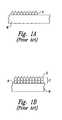
- FIGS. 1A and 1Bschematically illustrate the basic operation of ALD processes.
- a layer of gas molecules Acoats the surface of a workpiece W.
- the layer of A moleculesis formed by exposing the workpiece W to a precursor gas containing A molecules, and then purging the chamber with a purge gas to remove excess A molecules.
- This processcan form a monolayer of A molecules on the surface of the workpiece W because the A molecules at the surface are held in place during the purge cycle by physical adsorption forces at moderate temperatures or chemisorption forces at higher temperatures.
- the layer of A moleculesis then exposed to another precursor gas containing B molecules.
- the A moleculesreact with the B molecules to form an extremely thin layer of solid material C on the workpiece W.
- Such thin layersare typically less than 1 nm (and usually less than 2 ⁇ ) thick and are referred to herein as nanolayers.
- each cyclemay form a layer having a thickness of approximately 0.5-1.0 ⁇ .
- the chamberis then purged again with a purge gas to remove excess B molecules.
- ALDatomic layer deposition
- FIGS. 1A and 1Bare schematic cross-sectional views of stages in ALD processing in accordance with the prior art.
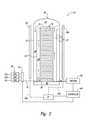
- FIG. 2is a schematic cross-sectional view of a microfeature workpiece processing system in accordance with an embodiment of the invention.
- FIG. 3is a flow chart schematically outlining aspects of a method in accordance with an embodiment of the invention.
- FIG. 4is a schematic illustration of one exemplary process for pretreating an inner surface of an ALD process chamber.
- FIG. 5is a schematic illustration of one exemplary process for depositing material on a surface of a microfeature workpiece.
- FIG. 6is a schematic illustration of an alternative process for depositing material on a surface of a microfeature workpiece.
- microfeature workpiece processing systems and methodsfor depositing materials onto microfeature workpieces. Many specific details of the invention are described below with reference to exemplary systems for depositing materials onto microfeature workpieces.
- microfeature workpieceis used throughout to include substrates upon which and/or in which microelectronic devices, micromechanical devices, data storage elements, read/write components, and other features are fabricated.
- microfeature workpiecescan be semiconductor wafers such as silicon or gallium arsenide wafers, glass substrates, insulative substrates, and many other types of materials.
- the microfeature workpiecestypically have submicron features with dimensions of 0.05 microns or greater.
- gasis used throughout to include any form of matter that has no fixed shape and will conform in volume to the space available, which specifically includes vapors (i.e., a gas having a temperature less than the critical temperature so that it may be liquefied or solidified by compression at a constant temperature).
- vaporsi.e., a gas having a temperature less than the critical temperature so that it may be liquefied or solidified by compression at a constant temperature.
- the first sectiondiscusses aspects of processing systems that may be used in accordance with selected embodiments of the invention.
- the second sectionoutlines methods in accordance with other aspects of the invention.
- FIG. 2schematically illustrates a reactor 10 in accordance with one embodiment of the invention.
- This reactor 10includes a processing enclosure 20 coupled to a gas supply 30 and a vacuum 40 .
- the processing enclosure 20generally includes an outer wall 22 and an annular liner 24 .
- a platform 60seals against the outer wall or some other part of the enclosure 20 to define a deposition chamber 25 .
- the liner 24functionally divides the deposition chamber 25 into a main chamber 28 and an annular exhaust 26 .
- the deposition chamber 25also includes inner surfaces 23 .
- the inner surfaces 23may comprise an inner surface of the outer wall 22 (including the dome at the top of the enclosure 20 ), the surfaces of at least a portion of the liner 24 , and the surfaces of the workpiece holder.
- microfeature workpieces We.g., semiconductor wafers
- a plurality of microfeature workpieces Wis held in the processing enclosure in a workpiece holder 70 .
- FIG. 3is merely schematic in nature and any number (e.g., 20-250) of workpieces W may be held in the workpiece holder 70 for simultaneous batch processing.
- the reactor 10also includes at least one heat source to heat the workpieces W and maintain them at the desired temperature.
- the heat source in FIG. 2is typified as a radiant heater 50 comprising a series of radiant heat panels 50 a and 50 b arranged about a circumference of the enclosure 20 to evenly heat the workpieces W.
- these heat panels 50 a - bcomprise quartz-halogen lamps or other types of radiative heat sources.
- other types of heat sourcesmay be employed.
- the heater 50may also include a power supply 52 that is coupled to the first heat panel 50 a by a first power line 54 a and to the second heat panel 50 b by a second power line 54 b.
- Gasis introduced from the gas supply 30 to the deposition chamber 25 by a gas line 32 and an inlet 36 .
- the inlet 36directs a flow of gas into the main chamber 28 of the deposition chamber 25 .
- gas introduced via the gas inlet 36will flow through the main chamber 28 , outwardly into the annular exhaust 26 , and out of the deposition chamber 25 .
- a valve assembly 34 in the gas line 32may be operated by a controller 90 to deliver gases to the deposition chamber 25 during the deposition phase.
- the controller 90comprises a computer having a programmable processor programmed to control operation of the reactor 10 to deposit material on the workpieces W in accordance with one or more of the methods outlined below.
- the controller 90may be coupled to the vacuum 40 to control its operation.
- the controller 90may also be operatively connected to the heater 50 , e.g., via the power supply 52 , to control the temperature of the workpieces W.
- the reactor 10is adapted to carry out an ALD process employing multiple precursors.
- the gas supply 30 in such embodimentscan include a plurality of separate gas sources 31 a - c and the valve assembly 34 may have a plurality of valves.
- the gas supply 30may include one or more precursors capable of reacting to deposit titanium nitride.
- the first gas source 31 ais adapted to deliver TiCl 4
- the second gas source 31 bis adapted to deliver NH 3
- the third gas source 31 cis adapted to deliver a flow of a purge gas, e.g., nitrogen.
- the first gas source 31 ais adapted to deliver an organotitanate, e.g., tetrakis(dimethylamido)titanium (TDMAT), and the second gas source 31 b is adapted to deliver a nitrogen carrier gas.
- the third gas source 31 cmay be omitted in the latter implementation, or the third gas supply 31 c may include a supply of SiH 4 or other material comprising silicon for purposes of depositing a layer of polysilicon in accordance with other aspects of the invention.
- embodiments of the inventionprovide methods for processing microfeature workpieces.
- FIG. 3schematically illustrates a manufacturing process 100 in accordance with one particular embodiment of the invention.
- aspects of the inventionpretreat the interior surface 23 of an ALD reactor 10 using chemical vapor deposition (CVD) and deposit materials on surfaces of microfeature workpieces via atomic layer deposition (ALD).
- CVDchemical vapor deposition
- ALDatomic layer deposition
- precursorsOne of the differences between a CVD process employing two or more precursors and an ALD process employing two or more precursors is the relative timing of the delivery of the precursors to the process chamber 25 .
- CVD processesboth of the precursors are simultaneously present in and react in a space adjacent a surface; in conventional ALD processes, the precursors are introduced separately and primarily react directly on the surface of the workpiece W.
- the manufacturing process 100 of FIG. 3starts at operation 102 with cleaning the interior surface 23 of the process chamber 25 . If the enclosure 20 of the reactor 10 is new, this operation 102 can be skipped. After the reactor 10 has been used for some time, though, material will build up on the inner surface 23 , which can adversely affect the quality of microfeature workpieces W treated in the process chamber 25 . Some or all of this material build-up can be removed in operation 102 in any suitable fashion. In one embodiment, the material build-up can be removed by exposing the interior of the process chamber 25 to a thermal etch or a plasma etch, e.g., a plasma of nitrogen trifluoride (NF 3 ). In some other circumstances, it may be advantageous to actually dip the outer wall 22 and/or the liner 24 of the enclosure 20 in an enchant liquid. Such cleaning procedures are well known in the art.
- FIG. 3schematically illustrates aspects of a chamber pretreatment process 110 in accordance with one embodiment of the invention.
- the chamber pretreatment process 110comprises depositing a coating, which may comprise at least one CVD-deposited layer of a pretreatment material.
- the chamber pretreatment process 110is carried out without a microfeature workpiece W in the process chamber 25 . This allows the pretreatment material to be deposited on the inner surface 23 of the process chamber 25 at an optimized rate without having to meet the stringent quality requirements for layer(s) of material deposited on microfeature workpieces W.
- the chamber pretreatment process 110may initially comprise depositing a layer of polycrystalline silicon (commonly referred to as “polysilicon” or just “poly”) on the inner surface 23 of the process chamber 25 (process 115 in FIG. 3 ). This may accomplished, for example, by heating the outer wall 22 and/or the inner wall 24 to a suitable temperature (e.g., about 550° C.) and delivering a silane gas (e.g., SiH 4 ) to the process chamber 25 .
- a suitable temperaturee.g., about 550° C.
- silane gase.g., SiH 4
- This polysilicon layerwill define a first layer of a coating formed on the inner surface 23 of the process chamber 25 and the pretreatment material formed in processes 120 - 125 may form the balance of the coating. It is anticipated that depositing a polysilicon layer before the pretreatment material will promote adhesion of the pretreatment material to the inner surface 23 .
- a first pretreatment precursor and a second pretreatment precursormay be introduced to the process chamber 25 contemporaneously, i.e., during an overlapping period of time.
- the first and second pretreatment precursorsmay be selected to deposit a desired pretreatment material on the inner surface 23 of the reaction chamber 25 via CVD.
- process conditions in the process chamber 25may be maintained to promote reaction of the precursors to deposit the pretreatment material on the inner surface 23 of the process chamber 25 .
- the first pretreatment precursorcomprises titanium and chlorine (e.g., TiCl 4 ) and the second pretreatment precursor comprises nitrogen (e.g., NH 3 ). Suitable temperatures, pressures, and flow rates of such gases to deposit TiN are well known and may be optimized readily by those skilled in the art.
- the flow of at least one of the precursors into the process chamber 25may be terminated.
- the thickness of this pretreatment materialmay be optimized for the particular process conditions employed to process workpieces in the ensuing steps of the manufacturing process 100 .
- the thickness of the pretreatment materialmay vary from one location on the inner surface 23 of the process chamber 25 to another.
- an average thickness of the TiN on an inner surface of the liner 24is less than 1000 ⁇ , e.g., about 500 ⁇ or less, with a thickness of about 100-200 ⁇ expected to work well for many applications.
- FIG. 4schematically illustrates one exemplary gas flow pattern for processes 120 and 125 of FIG. 3 .
- FIG. 4plots the flow rate of several gases over time.
- a gaseous first pretreatment precursor flow 121 and a gaseous second pretreatment precursor flow 122are contemporaneously delivered to the process chamber 25 of the reactor 10 .
- Thismay be accomplished by controlling the valve assembly 34 to deliver the first precursor, e.g., TiCl 4 , from the first gas source 31 a and the second precursor, e.g., NH 3 , from the second gas source 31 b.
- Both of these gasesare delivered to the main chamber 28 of the process chamber 25 via the gas inlet 36 and allowed to contact the inner surface 23 of the process chamber 25 .
- the first precursore.g., TiCl 4
- the second precursore.g., NH 3
- the first gas flow 121 and the second gas flow 122are shown as starting and ending at substantially the same time.
- the first gas flow 121may start before or after the second gas flow 122 is initiated and the first gas flow 121 may be terminated before or after the second gas flow 122 is terminated.
- the first gas flow 121 and the second gas flow 122may be said to be contemporaneous if they occur simultaneously over a material period of time, i.e., they need not start and/or stop at the same time.
- FIG. 4also schematically illustrates delivery of a purge/carrier gas flow 123 .
- the purge gasmay be delivered to the process chamber 25 before initiating the first and second gas flows 121 and 122 and again delivered after the first and second gas flows 121 and 122 are terminated.
- Such a purge gas flow 123may be used in conjunction with the vacuum 40 to purge any residual etchant (e.g., NF 3 ) from the process chamber 25 .
- the purge/carrier gasmay be delivered at the same time as the first and second gaseous precursors, in which case it serves as a more conventional carrier gas to provide adequate gas flow and to control the concentration of the precursors in the gas flow.
- the third gas flow 123may be delivered by selectively controlling the valve assembly 34 to deliver the purge gas from the third gas source 31 c to the gas inlet 36 .
- the chamber pretreatment process 110may also include introducing a reducing gas to the process chamber 25 in process 130 after the flow of at least one of the pretreatment precursors has been terminated in process 125 .
- the reducing gascan improve the quality of the pretreatment material deposited on the inner surface 23 of the reaction chamber 25 by serving as a “getter” of contaminants.
- the first and second pretreatment precursorscomprise TiCl 4 and NH 3
- some residual amount of chlorinemay be retained in the pretreatment material.
- Contacting this pretreatment material with a reducing gas at an appropriate temperaturecan remove at least some of the excess chlorine from the pretreatment material.
- the pretreatment materialis instead formed using an organotitanate (e.g., TDMAT) as the first precursor and nitrogen gas as the second precursor; delivering a reducing gas to the process chamber 25 in process 130 may help scavenge any carbon (e.g., in the form of TiC) included in the deposited TiN.
- organotitanatee.g., TDMAT
- nitrogen gasas the second precursor
- delivering a reducing gas to the process chamber 25 in process 130may help scavenge any carbon (e.g., in the form of TiC) included in the deposited TiN.
- the reducing gas employed in the optional treatment of process 130may comprise one or more of a variety of hydrogen-containing gases; hydrogen and ammonia are expected to be suitable reducing gases for many applications.
- ammoniaas the reducing gas can be particularly convenient in circumstances where ammonia is used as one of the pretreatment precursors in processes 120 - 125 .
- the pretreatment materialcomprises TiN deposited using TiCl 4 and NH 3 , for example, the reducing gas may be introduced in process 130 by terminating the flow of the TiCl 4 precursor and allowing the NH 3 flow to continue for an additional period of time.
- the process chamber 25may be cleaned intermittently. As discussed below, this cleaning process may be conducted after a fixed number (n max in process 190 ) of cycles for processing individual workpieces W (e.g., for single-workpiece systems) or batches of workpieces W (e.g., for the batch system shown in FIG. 2 ).
- a workpiece cycle counter nmay be reinitialized at zero in process 135 to reflect that no workpiece process cycles have been conducted in the reactor 10 since the cleaning 102 and pretreatment 110 of the processing chamber 25 .
- one or more microfeature workpiecesmay be positioned in the cleaned and pretreated process chamber 25 .
- embodiments of the inventionhave particular utility in batch ALD applications.
- a number of microfeature workpieces Wmay be positioned in a workpiece holder 70 and the workpiece holder 70 may be loaded in the process chamber 25 .
- a deposition productmay be deposited on the surface(s) of the microfeature workpiece(s) W in the process chamber 25 using an ALD process 150 .
- This ALD process 150may generally include introducing a quantity of the first deposition precursor (process 155 ), optionally purging the process chamber 25 (process 160 ), introducing a quantity of a second deposition precursor (process 165 ), and optionally purging the process chamber 25 again.
- This ALD deposition process 150may be carried out at processing conditions (e.g., temperature and flow rate) appropriate for the precursors selected.
- the ALD-deposited materialmay comprise a primary species that is the same as a primary species of the pretreatment material deposited in processes 120 - 130 of the chamber pretreatment process 110 .
- both the pretreatment material and the deposition product deposited on the microfeature workpieces in the ALD process 150may comprise TiN. If the primary species is the same for both of these deposited materials, the first and second pretreatment precursors introduced in process 120 may comprise the same precursors employed in the ALD process 150 .
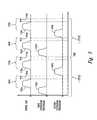
- FIG. 5is a schematic plot of gas flow rates as a function of time in accordance with one embodiment of the ALD process 150 of FIG. 3 .
- this ALD process 150discrete quantities of the first deposition precursor are delivered in first precursor pulses 155 a and 155 b.
- Discrete quantities of the second deposition precursorare delivered to the process chamber 25 in second precursor pulses 165 a and 165 b.
- the first pulses 155 and second pulses 165are delivered at different times in an alternating fashion.
- one pulse 155 a of the first precursormay be delivered to the process chamber 25 to contact the surfaces of the microfeature workpieces W.
- the precursormay be at least chemisorbed on the workpiece W. Theoretically, such chemisorbtion will form a monolayer that is uniformly one molecule thick on the entire surface of the workpiece W.
- Such a monolayermay be referred to as a saturated monolayer.
- some minor portions of the workpiece surfacemay not chemisorb a molecule of the precursor. Nevertheless, such imperfect monolayers are still referred to herein as monolayers.
- a substantially saturated monolayermay be suitable.
- a substantially saturated monolayeris a monolayer that will yield a deposited layer exhibiting the requisite quality and/or electrical properties.
- An excess of the first precursoris typically delivered to the process chamber 25 .
- This excess first precursorcan be purged from the vicinity of the workpiece surfaces in process 160 .
- Purgingmay involve a variety of techniques, including any combination of contacting the substrate and/or monolayer with a purge gas and/or lowering pressure in the process chamber 25 to below the pressure needed to deposit the precursor on the workpiece surface.
- suitable purge gasesinclude nitrogen, argon, helium, neon, krypton, and xenon.
- a first pulse 162 a of the purge gasis delivered to the process chamber 25 and a majority or all of this purge gas pulse 162 a may take place after the first precursor pulse 155 a is completed.
- the purge process shown in FIG. 5also includes a pump-down process 164 a wherein the vacuum 40 will withdraw gas from the process chamber 25 without introducing any additional gas from the gas supply 30 .
- the parameters of the purge pulse 162 a and pump-down 164 amay be determined experimentally, as known in the art.
- the pump-down time and/or the quantity of purge gas in the pulse 162 amay be successively reduced until the film growth rate increases. Such an increase in film growth rate may be deemed an indication that excess quantities of the first precursor remain in the process chamber 25 , which may be used to establish a minimum purge gas quantity and/or purge time.
- a pulse 165 a of the second gaseous precursormay be delivered to the process chamber 25 .
- This second precursormay chemisorb on the first monolayer of the first precursor and/or react with the monolayer to form a reaction product.
- This reaction productis typically one or no more than a few molecules thick, yielding a very thin, highly conformal nanolayer reaction product.
- the second precursor pulse 165 amay be terminated and the process chamber 25 may be purged again with a pulse 172 a of purge gas and/or a pump-down process 174 a.
- the pair of precursor pulses 155 a and 165 a, together with the associated pulses 162 a and 172 b of purge gas and/or pump-down processes 164 a and 174 b,may be considered one cycle.
- This cyclewill form a nanolayer that is usually thinner than the desired total thickness, with typical thicknesses of just 1 or 2 molecules (e.g., less than 1 nm, often less than 2 ⁇ ).
- the cycleis often repeated numerous times to yield a layer with an appropriate thickness.
- the manufacturing process 100 of FIG. 3may include determining in process 175 whether the material deposited on the microfeature workpieces W is thick enough.
- this determinationwill comprise determining whether a fixed number of ALD cycles, which has been empirically determined to deposit an adequate thickness, has been performed. If a sufficient thickness has not been deposited, the ALD process 150 may be repeated by returning to process 155 in FIG. 3 . This is illustrated in FIG. 5 as a second cycle that involves delivering a further pulse 155 b of the first precursor, purging the process chamber 25 with a further purge gas pulse 162 b and pump-down 164 b, subsequently delivering another second precursor pulse 165 b, and again purging the process chamber 25 with another purge gas pulse 172 b and pump-down 174 b. This ALD process 150 can be repeated as many times as necessary to yield a layer of the desired thickness.
- FIG. 6schematically illustrates a gas flow profile analogous to FIG. 5 , but illustrating an ALD process 151 in accordance with another embodiment of the invention.
- pulses 155 a - d of the first gaseous precursorare alternated with pulses 165 a - d of the second gaseous precursor.
- Thisis similar in some respects to the pulses 155 and 165 illustrated in FIG. 5 .
- the first pulse 165 a of the second gaseous precursormay immediately follow completion of the first pulse 155 a of the first gaseous precursor.
- next pulse 155 b of the first precursormay immediately follow termination of the first pulse 165 a of the second precursor.
- a monolayer of the first precursormay be deposited on the surface of the microfeature workpiece W prior to delivery of the pulse of the second precursor.
- some of the first precursormay remain in the vicinity of the workpiece W when the next pulse of the second gaseous precursor is initiated. This may result in a gaseous phase reaction between the precursors in a gaseous, unbound phase, leading to direct deposition of the reaction product on the surface of the workpiece W, and an increase in the rate of film formation.
- this CVD-like secondary depositionmay be held in check and may not significantly adversely affect the quality of the ALD-deposited material.
- the process chamber 25may be purged between some, but not all, precursor pulses.
- one pulse (e.g., 155 a ) of the first precursor and one pulse (e.g., 165 a ) of the second precursormay form one cycle of material deposition.
- a purge processwhich may comprise delivery of a purge gas and/or a pump-down of the process chamber 25 , may be performed between cycles to better promote deposition of a monolayer of the first precursor on the layer of material deposited in the previous cycle.
- the process 151 shown in FIG. 6may not technically conform to conventional definitions of atomic layer deposition because remnants of one precursor are present when the subsequent precursor is introduced. Nonetheless, it is anticipated that such a “pseudo-ALD” process may be useful in depositing some materials, e.g. layers of TiN.
- ALDis used herein to refer to both conventional ALD, (e.g., deposition via the process 150 illustrated in FIG. 5 ) and “pseudo-ALD” (e.g., deposition via the process 151 shown in FIG. 6 ).
- the ALD process 150may be repeated. If the deposited reaction product has a thickness at least as great as a target thickness (e.g., if the ALD process 150 has been repeated a fixed number of times), though, the microfeature workpiece W will be removed from the process chamber 25 in process 180 .
- the workpiece cycle counter nwhich was initialized at 0 in process 135 , may be incremented by one in process 185 to indicate that another workpiece cycle has been completed. In process 190 , the workpiece cycle counter n is compared to a fixed number n max of permissible cycles.
- the number n max of permissible cyclesmay be determined empirically to strike a balance between increasing throughput by reducing cleaning frequency and cleaning often enough to maintain an acceptable quality level of the processed microfeature workpieces W. If the number of batches of microfeature workpieces W treated is less than the maximum permissible number n max , another batch of microfeature workpieces W may be positioned in the process chamber 25 for processing (process 140 ). If the permissible number n max of workpiece batches has been processed, the process chamber 25 may be cleaned again in process 102 , starting the manufacturing process 100 again.
Landscapes
- Chemical & Material Sciences (AREA)
- General Chemical & Material Sciences (AREA)
- Chemical Kinetics & Catalysis (AREA)
- Engineering & Computer Science (AREA)
- Materials Engineering (AREA)
- Mechanical Engineering (AREA)
- Metallurgy (AREA)
- Organic Chemistry (AREA)
- Chemical Vapour Deposition (AREA)
Abstract
Description
- The present invention is related to equipment and methods for processing microfeature workpieces, e.g., semiconductor wafers. Aspects of the invention have particular utility in connection with deposition of materials on microfeature workpieces by atomic layer deposition.
- Thin film deposition techniques are widely used in the manufacturing of microfeatures to form a coating on a workpiece that closely conforms to the surface topography. In the context of microelectronic components, for example, the size of the individual components in the devices on a wafer is constantly decreasing, and the number of layers in the devices is increasing. As a result, the density of components and the aspect ratios of depressions (e.g., the ratio of the depth to the size of the opening) are increasing. Thin film deposition techniques accordingly strive to produce highly uniform conformal layers that cover the sidewalls, bottoms, and corners in deep depressions that have very small openings.
- One widely used thin film deposition technique is chemical vapor deposition (CVD). In a CVD system, one or more precursors that are capable of reacting to form a solid thin film are mixed in a gas or vapor state, and then the precursor mixture is presented to the surface of the workpiece. The surface of the workpiece catalyzes the reaction between the precursors to form a solid thin film at the workpiece surface. A common way to catalyze the reaction at the surface of the workpiece is to heat the workpiece to a temperature that causes the reaction. Such CVD processes are routinely employed in many stages of microelectronic component manufacture, for example.
- Thin layers of titanium nitride have utility in a number of applications. For example, the electrical conductivity of TiN makes it a useful component of microelectronic capacitors used in DRAM cells. (See, e.g., U.S. Pat. No. 6,211,033, the entirety of which is incorporated herein by reference, which suggests depositing titanium nitride or titanium carbonitride as part of a microelectronic capacitor electrode.) When processing individual wafers in single-wafer CVD reactors, the wafer is heated to the requisite reaction temperature by a heating plate in contact with the wafer.
- When the precursors are introduced to the chamber, a secondary deposit of the reaction product may accumulate on the walls of the process chamber as well. This reaction product will build up over time as successive microfeature workpieces are treated. This build-up can be uneven and can be subject to thermal stresses caused by the variations in temperature encountered when heating successive wafers to the requisite deposition temperature. Over time, the coating can degrade and begin to spall or shed particles that may render the finished workpieces commercially unsalable. In so-called “cold-wall” reactors, the walls of the reactor are cooler than the wafer and less of the reaction product may be deposited on the walls. Cold-wall reactors also reduce the thermal stresses on the secondary deposit by reducing the amplitude of the temperature cycle encountered in treating successive workpieces. Yet, even cold-wall reactors start to deposit particles on the workpieces after a time.
- To reduce the risk of particle contamination, the interior of the reaction chamber must be cleaned from time to time. For example, a plasma of an etchant gas (e.g., NF3) can be introduced to the chamber to remove the build-up from the chamber walls. Such plasma cleaning processes or thermal cleaning processes (also known in the art) can lead to other particle problems, though. For example, fluorine from NF3etchant gas can remain on the walls of the reactor and promote shedding of the secondary deposits on the chamber walls. As a result, the walls of these reactors are commonly conditioned after cleaning by applying a layer of the material to be deposited on the workpieces on the chamber wall before any workpieces are deposited.
- Single-wafer reactors have limited throughput. To increase throughput, CVD reactors may be adapted to process a plurality of wafers (e.g., 20-250) simultaneously in a batch process. Such batch CVD reactors have proven very cost-effective for many materials. For some other materials, though, batch CVD processes are not commercially viable. For example, attempts to develop batch CVD processes to deposit TiN on microfeature workpieces in commercial production have had little success. One of the problems encountered in batch TiN deposition via CVD is excessive particle generation. Even with a regular cleaning regimen, batch CVD reactors used to deposit TiN shed particles to the extent that product losses and quality control problems often outweigh the commercial advantages otherwise achievable in a batch process. Consequently, applying TiN films using batch CVD has met with very limited commercial acceptance.
- Atomic layer deposition (ALD) is a thin film deposition technique gaining prominence in deposition of TiN and other materials on microfeature workpieces.
FIGS. 1A and 1B schematically illustrate the basic operation of ALD processes. Referring toFIG. 1A , a layer of gas molecules A coats the surface of a workpiece W. The layer of A molecules is formed by exposing the workpiece W to a precursor gas containing A molecules, and then purging the chamber with a purge gas to remove excess A molecules. This process can form a monolayer of A molecules on the surface of the workpiece W because the A molecules at the surface are held in place during the purge cycle by physical adsorption forces at moderate temperatures or chemisorption forces at higher temperatures. The layer of A molecules is then exposed to another precursor gas containing B molecules. The A molecules react with the B molecules to form an extremely thin layer of solid material C on the workpiece W. Such thin layers are typically less than 1 nm (and usually less than 2 Å) thick and are referred to herein as nanolayers. For example, each cycle may form a layer having a thickness of approximately 0.5-1.0 Å. The chamber is then purged again with a purge gas to remove excess B molecules. - Films deposited via ALD tend to have higher purity and better conformality to microfeature topography than analogous films deposited via CVD. In addition, ALD is often carried out a lower temperature than CVD processes to deposit analogous materials, reducing thermal stresses on material built up on the inner surfaces of the process chamber. As a consequence, some of the difficulties encountered when depositing TiN in a batch CVD process can be ameliorated and batch ALD processing is garnering attention as a commercially viable process for depositing thin films of TiN on microfeature workpieces. Increasing throughput of batch ALD systems would further enhance the commercial benefit of such systems.
FIGS. 1A and 1B are schematic cross-sectional views of stages in ALD processing in accordance with the prior art.FIG. 2 is a schematic cross-sectional view of a microfeature workpiece processing system in accordance with an embodiment of the invention.FIG. 3 is a flow chart schematically outlining aspects of a method in accordance with an embodiment of the invention.FIG. 4 is a schematic illustration of one exemplary process for pretreating an inner surface of an ALD process chamber.FIG. 5 is a schematic illustration of one exemplary process for depositing material on a surface of a microfeature workpiece.FIG. 6 is a schematic illustration of an alternative process for depositing material on a surface of a microfeature workpiece.- A. Overview
- Various embodiments of the present invention provide microfeature workpiece processing systems and methods for depositing materials onto microfeature workpieces. Many specific details of the invention are described below with reference to exemplary systems for depositing materials onto microfeature workpieces. The term “microfeature workpiece” is used throughout to include substrates upon which and/or in which microelectronic devices, micromechanical devices, data storage elements, read/write components, and other features are fabricated. For example, microfeature workpieces can be semiconductor wafers such as silicon or gallium arsenide wafers, glass substrates, insulative substrates, and many other types of materials. The microfeature workpieces typically have submicron features with dimensions of 0.05 microns or greater. Furthermore, the term “gas” is used throughout to include any form of matter that has no fixed shape and will conform in volume to the space available, which specifically includes vapors (i.e., a gas having a temperature less than the critical temperature so that it may be liquefied or solidified by compression at a constant temperature). Several embodiments in accordance with the invention are set forth in
FIGS. 2-6 and the following text to provide a thorough understanding of particular embodiments of the invention. A person skilled in the art will understand, however, that the invention may have additional embodiments, or that the invention may be practiced without several of the details of the embodiments shown inFIGS. 2-6 . - For ease of understanding, the following discussion is subdivided into two areas of emphasis. The first section discusses aspects of processing systems that may be used in accordance with selected embodiments of the invention. The second section outlines methods in accordance with other aspects of the invention.
- B. Microfeature Workpiece Processing System
FIG. 2 schematically illustrates areactor 10 in accordance with one embodiment of the invention. Thisreactor 10 includes aprocessing enclosure 20 coupled to agas supply 30 and avacuum 40. Theprocessing enclosure 20 generally includes anouter wall 22 and anannular liner 24. Aplatform 60 seals against the outer wall or some other part of theenclosure 20 to define adeposition chamber 25. Theliner 24 functionally divides thedeposition chamber 25 into amain chamber 28 and anannular exhaust 26. Thedeposition chamber 25 also includesinner surfaces 23. Theinner surfaces 23 may comprise an inner surface of the outer wall22 (including the dome at the top of the enclosure20), the surfaces of at least a portion of theliner 24, and the surfaces of the workpiece holder.- One or more microfeature workpieces W, e.g., semiconductor wafers, may be positioned in the
deposition chamber 25 for processing. In the illustrated embodiment, a plurality of microfeature workpieces W is held in the processing enclosure in aworkpiece holder 70. It should be understood thatFIG. 3 is merely schematic in nature and any number (e.g., 20-250) of workpieces W may be held in theworkpiece holder 70 for simultaneous batch processing. - The
reactor 10 also includes at least one heat source to heat the workpieces W and maintain them at the desired temperature. The heat source inFIG. 2 is typified as aradiant heater 50 comprising a series ofradiant heat panels 50aand50barranged about a circumference of theenclosure 20 to evenly heat the workpieces W. In one embodiment, theseheat panels 50a-bcomprise quartz-halogen lamps or other types of radiative heat sources. In other embodiments, other types of heat sources may be employed. Theheater 50 may also include apower supply 52 that is coupled to the first heat panel50aby afirst power line 54aand to thesecond heat panel 50bby asecond power line 54b. - Gas is introduced from the
gas supply 30 to thedeposition chamber 25 by agas line 32 and aninlet 36. Theinlet 36 directs a flow of gas into themain chamber 28 of thedeposition chamber 25. Under influence of thevacuum 40, gas introduced via thegas inlet 36 will flow through themain chamber 28, outwardly into theannular exhaust 26, and out of thedeposition chamber 25. Avalve assembly 34 in thegas line 32 may be operated by acontroller 90 to deliver gases to thedeposition chamber 25 during the deposition phase. In one embodiment, thecontroller 90 comprises a computer having a programmable processor programmed to control operation of thereactor 10 to deposit material on the workpieces W in accordance with one or more of the methods outlined below. Thecontroller 90 may be coupled to thevacuum 40 to control its operation. Thecontroller 90 may also be operatively connected to theheater 50, e.g., via thepower supply 52, to control the temperature of the workpieces W. - Some aspects of the
gas supply 30 will depend on the nature of the deposition process to be carried out in thereactor 10. In one embodiment, thereactor 10 is adapted to carry out an ALD process employing multiple precursors. Thegas supply 30 in such embodiments can include a plurality of separate gas sources31a-cand thevalve assembly 34 may have a plurality of valves. For example, thegas supply 30 may include one or more precursors capable of reacting to deposit titanium nitride. In one such implementation, thefirst gas source 31ais adapted to deliver TiCl4, thesecond gas source 31bis adapted to deliver NH3, and thethird gas source 31cis adapted to deliver a flow of a purge gas, e.g., nitrogen. In another implementation, thefirst gas source 31ais adapted to deliver an organotitanate, e.g., tetrakis(dimethylamido)titanium (TDMAT), and thesecond gas source 31bis adapted to deliver a nitrogen carrier gas. Thethird gas source 31cmay be omitted in the latter implementation, or thethird gas supply 31cmay include a supply of SiH4or other material comprising silicon for purposes of depositing a layer of polysilicon in accordance with other aspects of the invention. - C. Methods for Processing Microfeature Workpieces
- As noted above, embodiments of the invention provide methods for processing microfeature workpieces. In the following discussion, reference is made to the
reactor 10 shown schematically inFIG. 2 . It should be understood, though, that reference to thisparticular reactor 10 is solely for purposes of illustration and that the methods outlined below are not limited to any particular processing system. FIG. 3 schematically illustrates amanufacturing process 100 in accordance with one particular embodiment of the invention. As discussed below, aspects of the invention pretreat theinterior surface 23 of anALD reactor 10 using chemical vapor deposition (CVD) and deposit materials on surfaces of microfeature workpieces via atomic layer deposition (ALD). Both CVD and ALD, as used herein, involve the use of at least one chemical species that can decompose or can react with another chemical species to form a desired material. Such chemical species are referred to herein as “precursors.” One of the differences between a CVD process employing two or more precursors and an ALD process employing two or more precursors is the relative timing of the delivery of the precursors to theprocess chamber 25. In CVD processes, both of the precursors are simultaneously present in and react in a space adjacent a surface; in conventional ALD processes, the precursors are introduced separately and primarily react directly on the surface of the workpiece W.- The
manufacturing process 100 ofFIG. 3 starts atoperation 102 with cleaning theinterior surface 23 of theprocess chamber 25. If theenclosure 20 of thereactor 10 is new, thisoperation 102 can be skipped. After thereactor 10 has been used for some time, though, material will build up on theinner surface 23, which can adversely affect the quality of microfeature workpieces W treated in theprocess chamber 25. Some or all of this material build-up can be removed inoperation 102 in any suitable fashion. In one embodiment, the material build-up can be removed by exposing the interior of theprocess chamber 25 to a thermal etch or a plasma etch, e.g., a plasma of nitrogen trifluoride (NF3). In some other circumstances, it may be advantageous to actually dip theouter wall 22 and/or theliner 24 of theenclosure 20 in an enchant liquid. Such cleaning procedures are well known in the art. - After the
inner surface 23 of theprocess chamber 25 has been suitably cleaned, theinner surface 23 can be pretreated, e.g., to reduce particle problems in subsequent ALD processing in thereactor 10.FIG. 3 schematically illustrates aspects of achamber pretreatment process 110 in accordance with one embodiment of the invention. Generally, thechamber pretreatment process 110 comprises depositing a coating, which may comprise at least one CVD-deposited layer of a pretreatment material. In some embodiments, thechamber pretreatment process 110 is carried out without a microfeature workpiece W in theprocess chamber 25. This allows the pretreatment material to be deposited on theinner surface 23 of theprocess chamber 25 at an optimized rate without having to meet the stringent quality requirements for layer(s) of material deposited on microfeature workpieces W. - In one embodiment, the
chamber pretreatment process 110 may initially comprise depositing a layer of polycrystalline silicon (commonly referred to as “polysilicon” or just “poly”) on theinner surface 23 of the process chamber25 (process 115 inFIG. 3 ). This may accomplished, for example, by heating theouter wall 22 and/or theinner wall 24 to a suitable temperature (e.g., about 550° C.) and delivering a silane gas (e.g., SiH4) to theprocess chamber 25. Techniques for depositing relatively high-quality layers of polysilicon using silane precursors is well known in the art. This polysilicon layer will define a first layer of a coating formed on theinner surface 23 of theprocess chamber 25 and the pretreatment material formed in processes120-125 may form the balance of the coating. It is anticipated that depositing a polysilicon layer before the pretreatment material will promote adhesion of the pretreatment material to theinner surface 23. - In
process 120, a first pretreatment precursor and a second pretreatment precursor may be introduced to theprocess chamber 25 contemporaneously, i.e., during an overlapping period of time. The first and second pretreatment precursors may be selected to deposit a desired pretreatment material on theinner surface 23 of thereaction chamber 25 via CVD. During introduction of the first and second pretreatment precursors inprocess 120, process conditions in theprocess chamber 25 may be maintained to promote reaction of the precursors to deposit the pretreatment material on theinner surface 23 of theprocess chamber 25. In one particular embodiment, the first pretreatment precursor comprises titanium and chlorine (e.g., TiCl4) and the second pretreatment precursor comprises nitrogen (e.g., NH3). Suitable temperatures, pressures, and flow rates of such gases to deposit TiN are well known and may be optimized readily by those skilled in the art. - After a suitable thickness of the pretreatment material is deposited on the
inner surface 23 of theprocess chamber 25, the flow of at least one of the precursors into theprocess chamber 25 may be terminated. The thickness of this pretreatment material may be optimized for the particular process conditions employed to process workpieces in the ensuing steps of themanufacturing process 100. The thickness of the pretreatment material may vary from one location on theinner surface 23 of theprocess chamber 25 to another. In some embodiments of the invention wherein the pretreatment material comprises TiN, though, an average thickness of the TiN on an inner surface of theliner 24 is less than 1000 Å, e.g., about 500 Å or less, with a thickness of about 100-200 Å expected to work well for many applications. FIG. 4 schematically illustrates one exemplary gas flow pattern forprocesses FIG. 3 . In particular,FIG. 4 plots the flow rate of several gases over time. In thisgas introduction process 120, a gaseous firstpretreatment precursor flow 121 and a gaseous secondpretreatment precursor flow 122 are contemporaneously delivered to theprocess chamber 25 of thereactor 10. This may be accomplished by controlling thevalve assembly 34 to deliver the first precursor, e.g., TiCl4, from thefirst gas source 31aand the second precursor, e.g., NH3, from thesecond gas source 31b.Both of these gases are delivered to themain chamber 28 of theprocess chamber 25 via thegas inlet 36 and allowed to contact theinner surface 23 of theprocess chamber 25. InFIG. 4 , thefirst gas flow 121 and thesecond gas flow 122 are shown as starting and ending at substantially the same time. In other embodiments, thefirst gas flow 121 may start before or after thesecond gas flow 122 is initiated and thefirst gas flow 121 may be terminated before or after thesecond gas flow 122 is terminated. In each of these cases, thefirst gas flow 121 and thesecond gas flow 122 may be said to be contemporaneous if they occur simultaneously over a material period of time, i.e., they need not start and/or stop at the same time.FIG. 4 also schematically illustrates delivery of a purge/carrier gas flow 123. In this embodiment, the purge gas may be delivered to theprocess chamber 25 before initiating the first and second gas flows121 and122 and again delivered after the first and second gas flows121 and122 are terminated. Such apurge gas flow 123 may be used in conjunction with thevacuum 40 to purge any residual etchant (e.g., NF3) from theprocess chamber 25. In other embodiments, the purge/carrier gas may be delivered at the same time as the first and second gaseous precursors, in which case it serves as a more conventional carrier gas to provide adequate gas flow and to control the concentration of the precursors in the gas flow. In the context ofFIG. 4 , thethird gas flow 123 may be delivered by selectively controlling thevalve assembly 34 to deliver the purge gas from thethird gas source 31cto thegas inlet 36.- As illustrated in
FIG. 3 , thechamber pretreatment process 110 may also include introducing a reducing gas to theprocess chamber 25 inprocess 130 after the flow of at least one of the pretreatment precursors has been terminated inprocess 125. The reducing gas can improve the quality of the pretreatment material deposited on theinner surface 23 of thereaction chamber 25 by serving as a “getter” of contaminants. For example, if the first and second pretreatment precursors comprise TiCl4and NH3, some residual amount of chlorine may be retained in the pretreatment material. Contacting this pretreatment material with a reducing gas at an appropriate temperature can remove at least some of the excess chlorine from the pretreatment material. In another embodiment, the pretreatment material is instead formed using an organotitanate (e.g., TDMAT) as the first precursor and nitrogen gas as the second precursor; delivering a reducing gas to theprocess chamber 25 inprocess 130 may help scavenge any carbon (e.g., in the form of TiC) included in the deposited TiN. (See, e.g., U.S. Pat. No. 5,956,613, the entirety of which is incorporated herein by reference.) The reducing gas employed in the optional treatment ofprocess 130 may comprise one or more of a variety of hydrogen-containing gases; hydrogen and ammonia are expected to be suitable reducing gases for many applications. Using ammonia as the reducing gas can be particularly convenient in circumstances where ammonia is used as one of the pretreatment precursors in processes120-125. If the pretreatment material comprises TiN deposited using TiCl4and NH3, for example, the reducing gas may be introduced inprocess 130 by terminating the flow of the TiCl4precursor and allowing the NH3flow to continue for an additional period of time. - In the
manufacturing process 100, theprocess chamber 25 may be cleaned intermittently. As discussed below, this cleaning process may be conducted after a fixed number (nmaxin process190) of cycles for processing individual workpieces W (e.g., for single-workpiece systems) or batches of workpieces W (e.g., for the batch system shown inFIG. 2 ). A workpiece cycle counter n may be reinitialized at zero inprocess 135 to reflect that no workpiece process cycles have been conducted in thereactor 10 since the cleaning102 andpretreatment 110 of theprocessing chamber 25. - In
process 140, one or more microfeature workpieces may be positioned in the cleaned and pretreatedprocess chamber 25. As noted above, embodiments of the invention have particular utility in batch ALD applications. In such embodiments, a number of microfeature workpieces W may be positioned in aworkpiece holder 70 and theworkpiece holder 70 may be loaded in theprocess chamber 25. - A deposition product may be deposited on the surface(s) of the microfeature workpiece(s) W in the
process chamber 25 using an ALD process150. This ALD process150 may generally include introducing a quantity of the first deposition precursor (process155), optionally purging the process chamber25 (process160), introducing a quantity of a second deposition precursor (process165), and optionally purging theprocess chamber 25 again. This ALD deposition process150 may be carried out at processing conditions (e.g., temperature and flow rate) appropriate for the precursors selected. In one embodiment, the ALD-deposited material may comprise a primary species that is the same as a primary species of the pretreatment material deposited in processes120-130 of thechamber pretreatment process 110. For example, both the pretreatment material and the deposition product deposited on the microfeature workpieces in the ALD process150 may comprise TiN. If the primary species is the same for both of these deposited materials, the first and second pretreatment precursors introduced inprocess 120 may comprise the same precursors employed in the ALD process150. FIG. 5 is a schematic plot of gas flow rates as a function of time in accordance with one embodiment of the ALD process150 ofFIG. 3 . In this ALD process150, discrete quantities of the first deposition precursor are delivered infirst precursor pulses process chamber 25 insecond precursor pulses first pulses 155 andsecond pulses 165 are delivered at different times in an alternating fashion.- Moving down the timeline of
FIG. 5 , onepulse 155aof the first precursor may be delivered to theprocess chamber 25 to contact the surfaces of the microfeature workpieces W. The precursor may be at least chemisorbed on the workpiece W. Theoretically, such chemisorbtion will form a monolayer that is uniformly one molecule thick on the entire surface of the workpiece W. Such a monolayer may be referred to as a saturated monolayer. As a practical matter, in some circumstances some minor portions of the workpiece surface may not chemisorb a molecule of the precursor. Nevertheless, such imperfect monolayers are still referred to herein as monolayers. In many applications, a substantially saturated monolayer may be suitable. A substantially saturated monolayer is a monolayer that will yield a deposited layer exhibiting the requisite quality and/or electrical properties. - An excess of the first precursor is typically delivered to the
process chamber 25. This excess first precursor can be purged from the vicinity of the workpiece surfaces inprocess 160. Purging may involve a variety of techniques, including any combination of contacting the substrate and/or monolayer with a purge gas and/or lowering pressure in theprocess chamber 25 to below the pressure needed to deposit the precursor on the workpiece surface. Examples of suitable purge gases include nitrogen, argon, helium, neon, krypton, and xenon. In the particular embodiment shown inFIG. 5 , afirst pulse 162aof the purge gas is delivered to theprocess chamber 25 and a majority or all of thispurge gas pulse 162amay take place after thefirst precursor pulse 155ais completed. The purge process shown inFIG. 5 also includes a pump-downprocess 164awherein thevacuum 40 will withdraw gas from theprocess chamber 25 without introducing any additional gas from thegas supply 30. The parameters of thepurge pulse 162aand pump-down164amay be determined experimentally, as known in the art. The pump-down time and/or the quantity of purge gas in thepulse 162amay be successively reduced until the film growth rate increases. Such an increase in film growth rate may be deemed an indication that excess quantities of the first precursor remain in theprocess chamber 25, which may be used to establish a minimum purge gas quantity and/or purge time. - Once the
process chamber 25 has been suitably purged, apulse 165aof the second gaseous precursor may be delivered to theprocess chamber 25. This second precursor may chemisorb on the first monolayer of the first precursor and/or react with the monolayer to form a reaction product. This reaction product is typically one or no more than a few molecules thick, yielding a very thin, highly conformal nanolayer reaction product. After a suitable exposure to the second gaseous precursor, thesecond precursor pulse 165amay be terminated and theprocess chamber 25 may be purged again with apulse 172aof purge gas and/or a pump-downprocess 174a. - As suggested in
FIG. 5 , the pair ofprecursor pulses pulses processes manufacturing process 100 ofFIG. 3 may include determining inprocess 175 whether the material deposited on the microfeature workpieces W is thick enough. In many circumstances, this determination will comprise determining whether a fixed number of ALD cycles, which has been empirically determined to deposit an adequate thickness, has been performed. If a sufficient thickness has not been deposited, the ALD process150 may be repeated by returning to process155 inFIG. 3 . This is illustrated inFIG. 5 as a second cycle that involves delivering afurther pulse 155bof the first precursor, purging theprocess chamber 25 with a furtherpurge gas pulse 162band pump-down164b,subsequently delivering anothersecond precursor pulse 165b,and again purging theprocess chamber 25 with anotherpurge gas pulse 172band pump-down174b.This ALD process150 can be repeated as many times as necessary to yield a layer of the desired thickness. FIG. 6 schematically illustrates a gas flow profile analogous toFIG. 5 , but illustrating an ALD process151 in accordance with another embodiment of the invention. In this ALD process151,pulses 155a-dof the first gaseous precursor are alternated withpulses 165a-dof the second gaseous precursor. This is similar in some respects to thepulses FIG. 5 . However, there is no purge process (160 or170 inFIG. 5 ) between delivery of successive quantities of the first and second precursors. Hence, inFIG. 6 , thefirst pulse 165aof the second gaseous precursor may immediately follow completion of thefirst pulse 155aof the first gaseous precursor. Likewise, thenext pulse 155bof the first precursor may immediately follow termination of thefirst pulse 165aof the second precursor. In this process, a monolayer of the first precursor may be deposited on the surface of the microfeature workpiece W prior to delivery of the pulse of the second precursor. Without the purge phase, though, some of the first precursor may remain in the vicinity of the workpiece W when the next pulse of the second gaseous precursor is initiated. This may result in a gaseous phase reaction between the precursors in a gaseous, unbound phase, leading to direct deposition of the reaction product on the surface of the workpiece W, and an increase in the rate of film formation. By appropriately selecting the process conditions and the timing of thepulses - In other embodiments, the
process chamber 25 may be purged between some, but not all, precursor pulses. For example, one pulse (e.g.,155a) of the first precursor and one pulse (e.g.,165a) of the second precursor may form one cycle of material deposition. A purge process, which may comprise delivery of a purge gas and/or a pump-down of theprocess chamber 25, may be performed between cycles to better promote deposition of a monolayer of the first precursor on the layer of material deposited in the previous cycle. - The process151 shown in
FIG. 6 may not technically conform to conventional definitions of atomic layer deposition because remnants of one precursor are present when the subsequent precursor is introduced. Nonetheless, it is anticipated that such a “pseudo-ALD” process may be useful in depositing some materials, e.g. layers of TiN. As a consequence, the term “ALD” is used herein to refer to both conventional ALD, (e.g., deposition via the process150 illustrated inFIG. 5 ) and “pseudo-ALD” (e.g., deposition via the process151 shown inFIG. 6 ). - As noted above, if the thickness of the material deposited via the ALD process150 is determined insufficient in
process 175, the ALD process150 may be repeated. If the deposited reaction product has a thickness at least as great as a target thickness (e.g., if the ALD process150 has been repeated a fixed number of times), though, the microfeature workpiece W will be removed from theprocess chamber 25 inprocess 180. The workpiece cycle counter n, which was initialized at 0 inprocess 135, may be incremented by one inprocess 185 to indicate that another workpiece cycle has been completed. Inprocess 190, the workpiece cycle counter n is compared to a fixed number nmaxof permissible cycles. The number nmaxof permissible cycles may be determined empirically to strike a balance between increasing throughput by reducing cleaning frequency and cleaning often enough to maintain an acceptable quality level of the processed microfeature workpieces W. If the number of batches of microfeature workpieces W treated is less than the maximum permissible number nmax, another batch of microfeature workpieces W may be positioned in theprocess chamber 25 for processing (process140). If the permissible number nmaxof workpiece batches has been processed, theprocess chamber 25 may be cleaned again inprocess 102, starting themanufacturing process 100 again. - The above-detailed embodiments of the invention are not intended to be exhaustive or to limit the invention to the precise form disclosed above. Specific embodiments of, and examples for, the invention are described above for illustrative purposes, but those skilled in the relevant art will recognize that various equivalent modifications are possible within the scope of the invention. For example, whereas steps are presented in a given order, alternative embodiments may perform steps in a different order. The various embodiments described herein can be combined to provide further embodiments.
- Unless the context clearly requires otherwise, throughout the description and the claims, the words “comprise,” “comprising,” and the like are to be construed in an inclusive sense as opposed to an exclusive or exhaustive sense, i.e., in a sense of “including, but not limited to.” Use of the word “or” in the claims in reference to a list of items is intended to cover a) any of the items in the list, b) all of the items in the list, and c) any combination of the items in the list.
- In general, the terms used in the following claims should not be construed to limit the invention to the specific embodiments disclosed in the specification unless the above-detailed description explicitly defines such terms. While certain aspects of the invention are presented below in certain claim forms, the inventors contemplate various aspects of the invention in any number of claim forms. Accordingly, the inventors reserve the right to add additional claims after filing the application to pursue such additional claim forms for other aspects of the invention.
Claims (27)
Priority Applications (1)
| Application Number | Priority Date | Filing Date | Title |
|---|---|---|---|
| US10/646,673US7344755B2 (en) | 2003-08-21 | 2003-08-21 | Methods and apparatus for processing microfeature workpieces; methods for conditioning ALD reaction chambers |
Applications Claiming Priority (1)
| Application Number | Priority Date | Filing Date | Title |
|---|---|---|---|
| US10/646,673US7344755B2 (en) | 2003-08-21 | 2003-08-21 | Methods and apparatus for processing microfeature workpieces; methods for conditioning ALD reaction chambers |
Publications (2)
| Publication Number | Publication Date |
|---|---|
| US20050039680A1true US20050039680A1 (en) | 2005-02-24 |
| US7344755B2 US7344755B2 (en) | 2008-03-18 |
Family
ID=34194588
Family Applications (1)
| Application Number | Title | Priority Date | Filing Date |
|---|---|---|---|
| US10/646,673Expired - LifetimeUS7344755B2 (en) | 2003-08-21 | 2003-08-21 | Methods and apparatus for processing microfeature workpieces; methods for conditioning ALD reaction chambers |
Country Status (1)
| Country | Link |
|---|---|
| US (1) | US7344755B2 (en) |
Cited By (32)
| Publication number | Priority date | Publication date | Assignee | Title |
|---|---|---|---|---|
| US20040049908A1 (en)* | 2002-01-15 | 2004-03-18 | Quallion Llc | Electric storage battery construction and method of manufacture |
| US20040226507A1 (en)* | 2003-04-24 | 2004-11-18 | Carpenter Craig M. | Methods for controlling mass flow rates and pressures in passageways coupled to reaction chambers and systems for depositing material onto microfeature workpieces in reaction chambers |
| US20050016984A1 (en)* | 2002-08-15 | 2005-01-27 | Dando Ross S. | Reactors with isolated gas connectors and methods for depositing materials onto micro-device workpieces |
| US20050022739A1 (en)* | 2002-07-08 | 2005-02-03 | Carpenter Craig M. | Apparatus and method for depositing materials onto microelectronic workpieces |
| US20050081786A1 (en)* | 2003-10-15 | 2005-04-21 | Kubista David J. | Systems for depositing material onto workpieces in reaction chambers and methods for removing byproducts from reaction chambers |
| US20050087302A1 (en)* | 2003-10-10 | 2005-04-28 | Mardian Allen P. | Apparatus and methods for manufacturing microfeatures on workpieces using plasma vapor processes |
| US20050087130A1 (en)* | 2003-10-09 | 2005-04-28 | Derderian Garo J. | Apparatus and methods for plasma vapor deposition processes |
| US20050126489A1 (en)* | 2003-12-10 | 2005-06-16 | Beaman Kevin L. | Methods and systems for controlling temperature during microfeature workpiece processing, e.g., CVD deposition |
| US20050164466A1 (en)* | 2004-01-28 | 2005-07-28 | Zheng Lingyi A. | Methods for forming small-scale capacitor structures |
| US20050249873A1 (en)* | 2004-05-05 | 2005-11-10 | Demetrius Sarigiannis | Apparatuses and methods for producing chemically reactive vapors used in manufacturing microelectronic devices |
| US20050249887A1 (en)* | 2004-05-06 | 2005-11-10 | Dando Ross S | Methods for depositing material onto microfeature workpieces in reaction chambers and systems for depositing materials onto microfeature workpieces |
| US20050268856A1 (en)* | 2004-06-02 | 2005-12-08 | Miller Matthew W | Reactors, systems and methods for depositing thin films onto microfeature workpieces |
| US20050287806A1 (en)* | 2004-06-24 | 2005-12-29 | Hiroyuki Matsuura | Vertical CVD apparatus and CVD method using the same |
| US20060060137A1 (en)* | 2004-09-22 | 2006-03-23 | Albert Hasper | Deposition of TiN films in a batch reactor |
| US20060115957A1 (en)* | 2003-09-17 | 2006-06-01 | Cem Basceri | Microfeature workpiece processing apparatus and methods for controlling deposition of materials on microfeature workpieces |
| US20060165873A1 (en)* | 2005-01-25 | 2006-07-27 | Micron Technology, Inc. | Plasma detection and associated systems and methods for controlling microfeature workpiece deposition processes |
| US20060196418A1 (en)* | 2005-03-04 | 2006-09-07 | Picosun Oy | Apparatuses and methods for deposition of material on surfaces |
| US20060205187A1 (en)* | 2003-08-28 | 2006-09-14 | Micron Technology, Inc. | Methods and apparatus for processing microfeature workpieces, e.g., for depositing materials on microfeature workpieces |
| US20060216947A1 (en)* | 2005-03-23 | 2006-09-28 | Samsung Electronics Co., Ltd. | Methods and batch type atomic layer deposition apparatus for forming dielectric films and methods of manufacturing metal-insulator-metal capacitors including the dielectric films |
| US20060237138A1 (en)* | 2005-04-26 | 2006-10-26 | Micron Technology, Inc. | Apparatuses and methods for supporting microelectronic devices during plasma-based fabrication processes |
| US7235138B2 (en) | 2003-08-21 | 2007-06-26 | Micron Technology, Inc. | Microfeature workpiece processing apparatus and methods for batch deposition of materials on microfeature workpieces |
| US7282239B2 (en) | 2003-09-18 | 2007-10-16 | Micron Technology, Inc. | Systems and methods for depositing material onto microfeature workpieces in reaction chambers |
| US7344755B2 (en) | 2003-08-21 | 2008-03-18 | Micron Technology, Inc. | Methods and apparatus for processing microfeature workpieces; methods for conditioning ALD reaction chambers |
| US20080286981A1 (en)* | 2007-05-14 | 2008-11-20 | Asm International N.V. | In situ silicon and titanium nitride deposition |
| US7481887B2 (en) | 2002-05-24 | 2009-01-27 | Micron Technology, Inc. | Apparatus for controlling gas pulsing in processes for depositing materials onto micro-device workpieces |
| US7584942B2 (en) | 2004-03-31 | 2009-09-08 | Micron Technology, Inc. | Ampoules for producing a reaction gas and systems for depositing materials onto microfeature workpieces in reaction chambers |
| US20090223448A1 (en)* | 2008-01-31 | 2009-09-10 | Hitachi Kokusai Electric Inc. | Substrate processing apparatus and method for manufacturing semiconductor device |
| US7691757B2 (en) | 2006-06-22 | 2010-04-06 | Asm International N.V. | Deposition of complex nitride films |
| US7833906B2 (en) | 2008-12-11 | 2010-11-16 | Asm International N.V. | Titanium silicon nitride deposition |
| WO2015144848A1 (en)* | 2014-03-27 | 2015-10-01 | Christof-Herbert Diener | Low-pressure plasma system with sequential control process |
| US20210242023A1 (en)* | 2020-01-31 | 2021-08-05 | Kokusai Electric Corporation | Method of manufacturing semiconductor device, non-transitory computer-readable recording medium and substrate processing apparatus |
| US20240191349A1 (en)* | 2022-12-12 | 2024-06-13 | Tokyo Electron Limited | Precoat method for substrate processing apparatus and substrate processing apparatus |
Families Citing this family (7)
| Publication number | Priority date | Publication date | Assignee | Title |
|---|---|---|---|---|
| JP3985899B2 (en)* | 2002-03-28 | 2007-10-03 | 株式会社日立国際電気 | Substrate processing equipment |
| PL2368811T3 (en) | 2010-03-23 | 2012-11-30 | Biscuit Gle | Resealable packaging for food products and method of manufacturing |
| US8597429B2 (en)* | 2011-01-18 | 2013-12-03 | Nuflare Technology, Inc. | Manufacturing apparatus and method for semiconductor device |
| JP6017396B2 (en)* | 2012-12-18 | 2016-11-02 | 東京エレクトロン株式会社 | Thin film forming method and thin film forming apparatus |
| US9873940B2 (en) | 2013-12-31 | 2018-01-23 | Lam Research Corporation | Coating system and method for coating interior fluid wetted surfaces of a component of a semiconductor substrate processing apparatus |
| US10100407B2 (en)* | 2014-12-19 | 2018-10-16 | Lam Research Corporation | Hardware and process for film uniformity improvement |
| US11804467B2 (en)* | 2020-06-25 | 2023-10-31 | Micron Technology, Inc. | Radiative heat collective bonder and gangbonder |
Citations (96)
| Publication number | Priority date | Publication date | Assignee | Title |
|---|---|---|---|---|
| US3634212A (en)* | 1970-05-06 | 1972-01-11 | M & T Chemicals Inc | Electrodeposition of bright acid tin and electrolytes therefor |
| US4313783A (en)* | 1980-05-19 | 1982-02-02 | Branson International Plasma Corporation | Computer controlled system for processing semiconductor wafers |
| US4436674A (en)* | 1981-07-30 | 1984-03-13 | J.C. Schumacher Co. | Vapor mass flow control system |
| US4438724A (en)* | 1982-08-13 | 1984-03-27 | Energy Conversion Devices, Inc. | Grooved gas gate |
| US4894132A (en)* | 1987-10-21 | 1990-01-16 | Mitsubishi Denki Kabushiki Kaisha | Sputtering method and apparatus |
| US4911638A (en)* | 1989-05-18 | 1990-03-27 | Direction Incorporated | Controlled diffusion environment capsule and system |
| US5091207A (en)* | 1989-07-20 | 1992-02-25 | Fujitsu Limited | Process and apparatus for chemical vapor deposition |
| US5090985A (en)* | 1989-10-17 | 1992-02-25 | Libbey-Owens-Ford Co. | Method for preparing vaporized reactants for chemical vapor deposition |
| US5286296A (en)* | 1991-01-10 | 1994-02-15 | Sony Corporation | Multi-chamber wafer process equipment having plural, physically communicating transfer means |
| US5377429A (en)* | 1993-04-19 | 1995-01-03 | Micron Semiconductor, Inc. | Method and appartus for subliming precursors |
| US5380396A (en)* | 1991-05-30 | 1995-01-10 | Hitachi, Ltd. | Valve and semiconductor fabricating equipment using the same |
| US5480818A (en)* | 1992-02-10 | 1996-01-02 | Fujitsu Limited | Method for forming a film and method for manufacturing a thin film transistor |
| US5496410A (en)* | 1992-03-10 | 1996-03-05 | Hitachi, Ltd. | Plasma processing apparatus and method of processing substrates by using same apparatus |
| US5498292A (en)* | 1994-06-16 | 1996-03-12 | Kishimoto Sangyo Co., Ltd. | Heating device used for a gas phase growing mechanism or heat treatment mechanism |
| US5500256A (en)* | 1994-08-16 | 1996-03-19 | Fujitsu Limited | Dry process apparatus using plural kinds of gas |
| US5592581A (en)* | 1993-07-19 | 1997-01-07 | Tokyo Electron Kabushiki Kaisha | Heat treatment apparatus |
| US5595606A (en)* | 1995-04-20 | 1997-01-21 | Tokyo Electron Limited | Shower head and film forming apparatus using the same |
| US5599513A (en)* | 1989-11-13 | 1997-02-04 | Showa Denko K.K. | Gas distribution plate for use with fluidized-bed gas-phase polymerizer |
| US5716796A (en)* | 1990-01-23 | 1998-02-10 | Medical Devices Corporation | Optical blood hemostatic analysis apparatus and method |
| US5729896A (en)* | 1996-10-31 | 1998-03-24 | International Business Machines Corporation | Method for attaching a flip chip on flexible circuit carrier using chip with metallic cap on solder |
| US5865417A (en)* | 1996-09-27 | 1999-02-02 | Redwood Microsystems, Inc. | Integrated electrically operable normally closed valve |
| US5866986A (en)* | 1996-08-05 | 1999-02-02 | Integrated Electronic Innovations, Inc. | Microwave gas phase plasma source |
| US5868159A (en)* | 1996-07-12 | 1999-02-09 | Mks Instruments, Inc. | Pressure-based mass flow controller |
| US5879459A (en)* | 1997-08-29 | 1999-03-09 | Genus, Inc. | Vertically-stacked process reactor and cluster tool system for atomic layer deposition |
| US5885425A (en)* | 1995-06-06 | 1999-03-23 | International Business Machines Corporation | Method for selective material deposition on one side of raised or recessed features |
| US6022483A (en)* | 1998-03-10 | 2000-02-08 | Intergrated Systems, Inc. | System and method for controlling pressure |
| US6032923A (en)* | 1998-01-08 | 2000-03-07 | Xerox Corporation | Fluid valves having cantilevered blocking films |
| US6039557A (en)* | 1989-12-22 | 2000-03-21 | Imarx Pharmaceutical Corp. | Apparatus for making gas-filled vesicles of optimal size |
| US6042652A (en)* | 1999-05-01 | 2000-03-28 | P.K. Ltd | Atomic layer deposition apparatus for depositing atomic layer on multiple substrates |
| US6174366B1 (en)* | 1993-12-23 | 2001-01-16 | Heikki Ihantola | Apparatus and method for processing of semiconductors, such as silicon chips |
| US6174809B1 (en)* | 1997-12-31 | 2001-01-16 | Samsung Electronics, Co., Ltd. | Method for forming metal layer using atomic layer deposition |
| US6174377B1 (en)* | 1997-03-03 | 2001-01-16 | Genus, Inc. | Processing chamber for atomic layer deposition processes |
| US6173673B1 (en)* | 1999-03-31 | 2001-01-16 | Tokyo Electron Limited | Method and apparatus for insulating a high power RF electrode through which plasma discharge gases are injected into a processing chamber |
| US6178660B1 (en)* | 1999-08-03 | 2001-01-30 | International Business Machines Corporation | Pass-through semiconductor wafer processing tool and process for gas treating a moving semiconductor wafer |
| US6183563B1 (en)* | 1998-05-18 | 2001-02-06 | Ips Ltd. | Apparatus for depositing thin films on semiconductor wafers |
| US6182603B1 (en)* | 1998-07-13 | 2001-02-06 | Applied Komatsu Technology, Inc. | Surface-treated shower head for use in a substrate processing chamber |
| US6190459B1 (en)* | 1998-01-07 | 2001-02-20 | Tokyo Electron Limited | Gas treatment apparatus |
| US6194628B1 (en)* | 1995-09-25 | 2001-02-27 | Applied Materials, Inc. | Method and apparatus for cleaning a vacuum line in a CVD system |
| US6193802B1 (en)* | 1995-09-25 | 2001-02-27 | Applied Materials, Inc. | Parallel plate apparatus for in-situ vacuum line cleaning for substrate processing equipment |
| US6192827B1 (en)* | 1998-07-03 | 2001-02-27 | Applied Materials, Inc. | Double slit-valve doors for plasma processing |
| US6197119B1 (en)* | 1999-02-18 | 2001-03-06 | Mks Instruments, Inc. | Method and apparatus for controlling polymerized teos build-up in vacuum pump lines |
| US6200415B1 (en)* | 1999-06-30 | 2001-03-13 | Lam Research Corporation | Load controlled rapid assembly clamp ring |
| US6203613B1 (en)* | 1999-10-19 | 2001-03-20 | International Business Machines Corporation | Atomic layer deposition with nitrate containing precursors |
| US6206972B1 (en)* | 1999-07-08 | 2001-03-27 | Genus, Inc. | Method and apparatus for providing uniform gas delivery to substrates in CVD and PECVD processes |
| US6206967B1 (en)* | 1997-12-02 | 2001-03-27 | Applied Materials, Inc. | Low resistivity W using B2H6 nucleation step |
| US6207937B1 (en)* | 1998-05-11 | 2001-03-27 | Semitool, Inc. | Temperature control system for a thermal reactor |
| US6334928B1 (en)* | 1998-01-30 | 2002-01-01 | Kabushiki Kaisha Toshiba | Semiconductor processing system and method of using the same |
| US20020000202A1 (en)* | 2000-06-29 | 2002-01-03 | Katsuhisa Yuda | Remote plasma apparatus for processing sustrate with two types of gases |
| US20020007790A1 (en)* | 2000-07-22 | 2002-01-24 | Park Young-Hoon | Atomic layer deposition (ALD) thin film deposition equipment having cleaning apparatus and cleaning method |
| US6342277B1 (en)* | 1996-08-16 | 2002-01-29 | Licensee For Microelectronics: Asm America, Inc. | Sequential chemical vapor deposition |
| US6346477B1 (en)* | 2001-01-09 | 2002-02-12 | Research Foundation Of Suny - New York | Method of interlayer mediated epitaxy of cobalt silicide from low temperature chemical vapor deposition of cobalt |
| US6347602B2 (en)* | 1998-06-04 | 2002-02-19 | Tokyo Electron Limited | Plasma processing apparatus |
| US6347918B1 (en)* | 1999-01-27 | 2002-02-19 | Applied Materials, Inc. | Inflatable slit/gate valve |
| US20020020353A1 (en)* | 1996-10-30 | 2002-02-21 | Redemann Eric J. | Gas panel |
| US6355561B1 (en)* | 2000-11-21 | 2002-03-12 | Micron Technology, Inc. | ALD method to improve surface coverage |
| US6358323B1 (en)* | 1998-07-21 | 2002-03-19 | Applied Materials, Inc. | Method and apparatus for improved control of process and purge material in a substrate processing system |
| US20030003697A1 (en)* | 2000-06-08 | 2003-01-02 | Micron Techology, Inc. | Methods for forming and integrated circuit structures containing ruthenium and tungsten containing layers |
| US20030003730A1 (en)* | 2001-02-13 | 2003-01-02 | Micron Technology, Inc. | Sequential pulse deposition |
| US6503330B1 (en)* | 1999-12-22 | 2003-01-07 | Genus, Inc. | Apparatus and method to achieve continuous interface and ultrathin film during atomic layer deposition |
| US6506254B1 (en)* | 2000-06-30 | 2003-01-14 | Lam Research Corporation | Semiconductor processing equipment having improved particle performance |
| US20030013320A1 (en)* | 2001-05-31 | 2003-01-16 | Samsung Electronics Co., Ltd. | Method of forming a thin film using atomic layer deposition |
| US6508268B1 (en)* | 1998-11-13 | 2003-01-21 | Ckd Corporation | Vacuum pressure control apparatus |
| US6509280B2 (en)* | 2001-02-22 | 2003-01-21 | Samsung Electronics Co., Ltd. | Method for forming a dielectric layer of a semiconductor device |
| US20030023338A1 (en)* | 2001-07-27 | 2003-01-30 | Applied Materials, Inc. | Atomic layer deposition apparatus |
| US20030024477A1 (en)* | 2001-08-02 | 2003-02-06 | Hitachi Kokusai Electric Inc. | Substrate processing apparatus |
| US20030027428A1 (en)* | 2001-07-18 | 2003-02-06 | Applied Materials, Inc. | Bypass set up for integration of remote optical endpoint for CVD chamber |
| US20030031794A1 (en)* | 1997-12-24 | 2003-02-13 | Kunihiro Tada | Method of forming titanium film by CVD |
| US20030037730A1 (en)* | 1999-03-11 | 2003-02-27 | Tokyo Electron Limited | Processing system, evacuating system for processing system, low-pressure CVD system, and evacuating system and trapping device for low-pressure CVD system |
| US20030037729A1 (en)* | 2001-07-13 | 2003-02-27 | Dedontney Jay Brian | Modular injector and exhaust assembly |
| US20030049372A1 (en)* | 1997-08-11 | 2003-03-13 | Cook Robert C. | High rate deposition at low pressures in a small batch reactor |
| US6534007B1 (en)* | 1997-08-01 | 2003-03-18 | Applied Komatsu Technology, Inc. | Method and apparatus for detecting the endpoint of a chamber cleaning |
| US6534395B2 (en)* | 2000-03-07 | 2003-03-18 | Asm Microchemistry Oy | Method of forming graded thin films using alternating pulses of vapor phase reactants |
| US20030060030A1 (en)* | 2001-09-25 | 2003-03-27 | Kwang-Myung Lee | Method for processing a wafer and apparatus for performing the same |
| US20040000270A1 (en)* | 2002-06-26 | 2004-01-01 | Carpenter Craig M. | Methods and apparatus for vapor processing of micro-device workpieces |
| US6673196B1 (en)* | 1999-09-02 | 2004-01-06 | Tokyo Electron Limited | Plasma processing apparatus |
| US20040003777A1 (en)* | 2002-07-08 | 2004-01-08 | Carpenter Craig M. | Apparatus and method for depositing materials onto microelectronic workpieces |
| US20040007188A1 (en)* | 2000-08-22 | 2004-01-15 | Novellus Systems, Inc. | Gas-purged vacuum valve |
| US6689220B1 (en)* | 2000-11-22 | 2004-02-10 | Simplus Systems Corporation | Plasma enhanced pulsed layer deposition |
| US20040025786A1 (en)* | 2002-04-05 | 2004-02-12 | Tadashi Kontani | Substrate processing apparatus and reaction container |
| US20040035358A1 (en)* | 2002-08-23 | 2004-02-26 | Cem Basceri | Reactors having gas distributors and methods for depositing materials onto micro-device workpieces |
| US20040040503A1 (en)* | 2002-08-29 | 2004-03-04 | Micron Technology, Inc. | Micromachines for delivering precursors and gases for film deposition |
| US20040040502A1 (en)* | 2002-08-29 | 2004-03-04 | Micron Technology, Inc. | Micromachines for delivering precursors and gases for film deposition |
| US6704913B2 (en)* | 2001-01-26 | 2004-03-09 | Applied Materials Inc. | In situ wafer heat for reduced backside contamination |
| US6705345B1 (en)* | 1999-11-08 | 2004-03-16 | The Trustees Of Boston University | Micro valve arrays for fluid flow control |
| US6706334B1 (en)* | 1997-06-04 | 2004-03-16 | Tokyo Electron Limited | Processing method and apparatus for removing oxide film |
| US6838114B2 (en)* | 2002-05-24 | 2005-01-04 | Micron Technology, Inc. | Methods for controlling gas pulsing in processes for depositing materials onto micro-device workpieces |
| US6845734B2 (en)* | 2002-04-11 | 2005-01-25 | Micron Technology, Inc. | Deposition apparatuses configured for utilizing phased microwave radiation |
| US20050016956A1 (en)* | 2003-03-14 | 2005-01-27 | Xinye Liu | Methods and apparatus for cycle time improvements for atomic layer deposition |
| US20050016984A1 (en)* | 2002-08-15 | 2005-01-27 | Dando Ross S. | Reactors with isolated gas connectors and methods for depositing materials onto micro-device workpieces |
| US6849131B2 (en)* | 2002-10-05 | 2005-02-01 | Taiwan Semiconductor Manufacturing Co., Ltd | Truncated dummy plate for process furnace |
| US20050028734A1 (en)* | 2003-02-11 | 2005-02-10 | Carpenter Craig M. | Reactors with isolated gas connectors and methods for depositing materials onto micro-device workpieces |
| US20050039686A1 (en)* | 2003-08-21 | 2005-02-24 | Zheng Lingyi A. | Microfeature workpiece processing apparatus and methods for batch deposition of materials on microfeature workpieces |
| US20050045100A1 (en)* | 2003-03-03 | 2005-03-03 | Derderian Garo J. | Reactors, systems with reaction chambers, and methods for depositing materials onto micro-device workpieces |
| US20050045102A1 (en)* | 2003-08-28 | 2005-03-03 | Zheng Lingyi A. | Methods and apparatus for processing microfeature workpieces, e.g., for depositing materials on microfeature workpieces |
| US20050048742A1 (en)* | 2003-08-26 | 2005-03-03 | Tokyo Electron Limited | Multiple grow-etch cyclic surface treatment for substrate preparation |
| US6991684B2 (en)* | 2000-09-29 | 2006-01-31 | Tokyo Electron Limited | Heat-treating apparatus and heat-treating method |
Family Cites Families (274)
| Publication number | Priority date | Publication date | Assignee | Title |
|---|---|---|---|---|
| FR1500185A (en) | 1966-08-08 | 1967-11-03 | Ct De Rech S Du Fer Blanc | Electrolytic tinning process of a steel strip |
| GB1260300A (en) | 1968-04-24 | 1972-01-12 | Plessey Co Ltd | IMPROVEMENTS IN OR RELATING TO THE PRODUCTION OF VAPOUR-DEPOSITED Nb3Sn CONDUCTOR MATERIAL |
| US3618919A (en) | 1969-11-03 | 1971-11-09 | Btu Eng Corp | Adjustable heat and gas barrier |
| US3630881A (en) | 1970-01-22 | 1971-12-28 | Ibm | Cathode-target assembly for rf sputtering apparatus |
| SU598630A1 (en) | 1974-08-15 | 1978-02-21 | Предприятие П/Я Р-6707 | Device for introducing into reaction chamber |
| US4018949A (en) | 1976-01-12 | 1977-04-19 | Ford Motor Company | Selective tin deposition onto aluminum piston skirt areas |
| US4289061A (en) | 1977-10-03 | 1981-09-15 | Hooker Chemicals & Plastics Corp. | Device and assembly for mounting parts |
| US4242182A (en) | 1978-07-21 | 1980-12-30 | Francine Popescu | Bright tin electroplating bath |
| NL184695C (en) | 1978-12-04 | 1989-10-02 | Philips Nv | BATH FOR THE STREAMLESS DEPOSIT OF TIN ON SUBSTRATES. |
| JPS55158623A (en) | 1979-05-29 | 1980-12-10 | Hitachi Ltd | Method of controlling semiconductor vapor phase growth |
| JPS5747706A (en) | 1980-09-04 | 1982-03-18 | Toshio Hirai | Lump of silicon nitride containing ti and its manufacture |
| US4545136A (en) | 1981-03-16 | 1985-10-08 | Sovonics Solar Systems | Isolation valve |
| DD206687A3 (en) | 1981-07-28 | 1984-02-01 | Mikroelektronik Zt Forsch Tech | METHOD AND DEVICE FOR FUELING LP CVD PROCESSES IN A PIPE REACTOR |
| US4826579A (en) | 1982-06-25 | 1989-05-02 | Cel Systems Corporation | Electrolytic preparation of tin and other metals |
| US4397753A (en) | 1982-09-20 | 1983-08-09 | Circuit Chemistry Corporation | Solder stripping solution |
| US4593644A (en) | 1983-10-26 | 1986-06-10 | Rca Corporation | Continuous in-line deposition system |
| GB2162207B (en) | 1984-07-26 | 1989-05-10 | Japan Res Dev Corp | Semiconductor crystal growth apparatus |
| US4590042A (en) | 1984-12-24 | 1986-05-20 | Tegal Corporation | Plasma reactor having slotted manifold |
| US5769950A (en) | 1985-07-23 | 1998-06-23 | Canon Kabushiki Kaisha | Device for forming deposited film |
| DE3709066A1 (en) | 1986-03-31 | 1987-10-01 | Toshiba Kawasaki Kk | METHOD FOR PRODUCING A THIN METAL FILM BY CHEMICAL EVAPORATION |
| JPH0616491B2 (en) | 1986-04-07 | 1994-03-02 | 日本電気株式会社 | Vapor phase epitaxial growth system |
| US4681777A (en) | 1986-05-05 | 1987-07-21 | Engelken Robert D | Method for electroless and vapor deposition of thin films of three tin sulfide phases on conductive and nonconductive substrates |
| JPS62263629A (en) | 1986-05-12 | 1987-11-16 | Hitachi Ltd | Vapor phase growth equipment |
| JPS6320490A (en) | 1986-07-14 | 1988-01-28 | Toshiba Corp | Cleaning method for film forming equipment |
| US4966646A (en) | 1986-09-24 | 1990-10-30 | Board Of Trustees Of Leland Stanford University | Method of making an integrated, microminiature electric-to-fluidic valve |
| JPS63111177A (en) | 1986-10-29 | 1988-05-16 | Hitachi Ltd | Microwave plasma thin film forming equipment |
| JPS63234198A (en) | 1987-03-24 | 1988-09-29 | 株式会社東芝 | Flange image leakage detection device |
| JPS63256460A (en) | 1987-04-14 | 1988-10-24 | Oki Electric Ind Co Ltd | Substrate for thermal head and production thereof |
| JPH0777211B2 (en) | 1987-08-19 | 1995-08-16 | 富士通株式会社 | Ashing method |
| JPH0626188B2 (en) | 1987-09-24 | 1994-04-06 | 日本電気株式会社 | Vapor phase growth equipment |
| JPH0668962B2 (en) | 1987-12-21 | 1994-08-31 | 株式会社東芝 | Vacuum device and method of performing process using the same |
| JP2792030B2 (en) | 1988-04-26 | 1998-08-27 | 石川島播磨重工業株式会社 | Furnace sealing equipment |
| DE3830249A1 (en) | 1988-09-06 | 1990-03-15 | Schott Glaswerke | PLASMA PROCESS FOR COATING LEVEL SUBSTRATES |
| US4949669A (en) | 1988-12-20 | 1990-08-21 | Texas Instruments Incorporated | Gas flow systems in CCVD reactors |
| US5076205A (en) | 1989-01-06 | 1991-12-31 | General Signal Corporation | Modular vapor processor system |
| US5015330A (en) | 1989-02-28 | 1991-05-14 | Kabushiki Kaisha Toshiba | Film forming method and film forming device |
| US5020476A (en) | 1990-04-17 | 1991-06-04 | Ds Research, Inc. | Distributed source assembly |
| US4977106A (en) | 1990-05-01 | 1990-12-11 | Texas Instruments Incorporated | Tin chemical vapor deposition using TiCl4 and SiH4 |
| US5212116A (en) | 1990-06-18 | 1993-05-18 | At&T Bell Laboratories | Method for forming planarized films by preferential etching of the center of a wafer |
| US5136975A (en) | 1990-06-21 | 1992-08-11 | Watkins-Johnson Company | Injector and method for delivering gaseous chemicals to a surface |
| US5131752A (en) | 1990-06-28 | 1992-07-21 | Tamarack Scientific Co., Inc. | Method for film thickness endpoint control |
| US5223113A (en) | 1990-07-20 | 1993-06-29 | Tokyo Electron Limited | Apparatus for forming reduced pressure and for processing object |
| JPH04100533A (en) | 1990-08-18 | 1992-04-02 | Mitsubishi Electric Corp | vacuum container |
| US5325020A (en) | 1990-09-28 | 1994-06-28 | Abtox, Inc. | Circular waveguide plasma microwave sterilizer apparatus |
| JPH04213818A (en) | 1990-12-07 | 1992-08-04 | Sony Corp | Cvd device |
| JP2972422B2 (en) | 1990-12-28 | 1999-11-08 | 北海製罐株式会社 | Welding can body |
| US5062446A (en) | 1991-01-07 | 1991-11-05 | Sematech, Inc. | Intelligent mass flow controller |
| JP2787142B2 (en) | 1991-03-01 | 1998-08-13 | 上村工業 株式会社 | Electroless tin, lead or their alloy plating method |
| US5232749A (en) | 1991-04-30 | 1993-08-03 | Micron Technology, Inc. | Formation of self-limiting films by photoemission induced vapor deposition |
| JPH081923B2 (en) | 1991-06-24 | 1996-01-10 | ティーディーケイ株式会社 | Clean transfer method and device |
| JP3238432B2 (en) | 1991-08-27 | 2001-12-17 | 東芝機械株式会社 | Multi-chamber type single wafer processing equipment |
| US5200023A (en) | 1991-08-30 | 1993-04-06 | International Business Machines Corp. | Infrared thermographic method and apparatus for etch process monitoring and control |
| US5172849A (en) | 1991-09-25 | 1992-12-22 | General Motors Corporation | Method and apparatus for convection brazing of aluminum heat exchangers |
| JP2989063B2 (en) | 1991-12-12 | 1999-12-13 | キヤノン株式会社 | Thin film forming apparatus and thin film forming method |
| JP3371230B2 (en) | 1992-11-09 | 2003-01-27 | 東京エレクトロン株式会社 | Transport processing equipment |
| JPH06295862A (en) | 1992-11-20 | 1994-10-21 | Mitsubishi Electric Corp | Compound semiconductor fabrication system and organic metal material vessel |
| US5453124A (en) | 1992-12-30 | 1995-09-26 | Texas Instruments Incorporated | Programmable multizone gas injector for single-wafer semiconductor processing equipment |
| JPH06201539A (en) | 1993-01-04 | 1994-07-19 | Yasuo Kitsuta | Centrifugal evaporator |
| US5932286A (en) | 1993-03-16 | 1999-08-03 | Applied Materials, Inc. | Deposition of silicon nitride thin films |
| JP3013652B2 (en) | 1993-06-01 | 2000-02-28 | 富士通株式会社 | Exhaust device and its cleaning method |
| JP3288490B2 (en) | 1993-07-09 | 2002-06-04 | 富士通株式会社 | Semiconductor device manufacturing method and semiconductor device manufacturing apparatus |
| US5626936A (en) | 1993-09-09 | 1997-05-06 | Energy Pillow, Inc. | Phase change insulation system |
| US5427666A (en) | 1993-09-09 | 1995-06-27 | Applied Materials, Inc. | Method for in-situ cleaning a Ti target in a Ti + TiN coating process |
| JP3394293B2 (en) | 1993-09-20 | 2003-04-07 | 株式会社日立製作所 | Method for transporting sample and method for manufacturing semiconductor device |
| US5433835B1 (en) | 1993-11-24 | 1997-05-20 | Applied Materials Inc | Sputtering device and target with cover to hold cooling fluid |
| KR950020993A (en) | 1993-12-22 | 1995-07-26 | 김광호 | Semiconductor manufacturing device |
| EP0665577A1 (en) | 1994-01-28 | 1995-08-02 | Applied Materials, Inc. | Method and apparatus for monitoring the deposition rate of films during physical vapour deposition |
| US5589002A (en) | 1994-03-24 | 1996-12-31 | Applied Materials, Inc. | Gas distribution plate for semiconductor wafer processing apparatus with means for inhibiting arcing |
| US5900103A (en) | 1994-04-20 | 1999-05-04 | Tokyo Electron Limited | Plasma treatment method and apparatus |
| US5522934A (en) | 1994-04-26 | 1996-06-04 | Tokyo Electron Limited | Plasma processing apparatus using vertical gas inlets one on top of another |
| KR960002534A (en) | 1994-06-07 | 1996-01-26 | 이노우에 아키라 | Pressure reducing and atmospheric pressure treatment device |
| US5418180A (en) | 1994-06-14 | 1995-05-23 | Micron Semiconductor, Inc. | Process for fabricating storage capacitor structures using CVD tin on hemispherical grain silicon |
| ES2163559T3 (en) | 1994-06-24 | 2002-02-01 | Nisshin Steel Co Ltd | JOINT ASSEMBLY FOR THERMAL TREATMENT OVENS USING AN ATMOSPHERIC GAS CONTAINING GASEOUS HYDROGEN. |
| US5643394A (en) | 1994-09-16 | 1997-07-01 | Applied Materials, Inc. | Gas injection slit nozzle for a plasma process reactor |
| JP3473715B2 (en) | 1994-09-30 | 2003-12-08 | 信越半導体株式会社 | Quartz glass wafer boat |
| JP3417751B2 (en) | 1995-02-13 | 2003-06-16 | 株式会社東芝 | Method for manufacturing semiconductor device |
| JP3246708B2 (en) | 1995-05-02 | 2002-01-15 | 東京エレクトロン株式会社 | Trap device and unreacted process gas exhaust mechanism using the same |
| US5654589A (en) | 1995-06-06 | 1997-08-05 | Advanced Micro Devices, Incorporated | Landing pad technology doubled up as local interconnect and borderless contact for deep sub-half micrometer IC application |
| US5640751A (en) | 1995-07-17 | 1997-06-24 | Thermionics Laboratories, Inc. | Vacuum flange |
| JPH0945624A (en) | 1995-07-27 | 1997-02-14 | Tokyo Electron Ltd | Leaf-type heat treating system |
| JP3507220B2 (en) | 1995-09-14 | 2004-03-15 | 株式会社日立国際電気 | Semiconductor manufacturing equipment |
| US5997588A (en) | 1995-10-13 | 1999-12-07 | Advanced Semiconductor Materials America, Inc. | Semiconductor processing system with gas curtain |
| TW356554B (en) | 1995-10-23 | 1999-04-21 | Watkins Johnson Co | Gas injection system for semiconductor processing |
| US5801104A (en) | 1995-10-24 | 1998-09-01 | Micron Technology, Inc. | Uniform dielectric film deposition on textured surfaces |
| US5536317A (en) | 1995-10-27 | 1996-07-16 | Specialty Coating Systems, Inc. | Parylene deposition apparatus including a quartz crystal thickness/rate controller |
| US5792269A (en) | 1995-10-31 | 1998-08-11 | Applied Materials, Inc. | Gas distribution for CVD systems |
| JP3768575B2 (en) | 1995-11-28 | 2006-04-19 | アプライド マテリアルズ インコーポレイテッド | CVD apparatus and chamber cleaning method |
| US5956613A (en) | 1995-12-27 | 1999-09-21 | Lsi Logic Corporation | Method for improvement of TiN CVD film quality |
| US6663713B1 (en) | 1996-01-08 | 2003-12-16 | Applied Materials Inc. | Method and apparatus for forming a thin polymer layer on an integrated circuit structure |
| US5754390A (en) | 1996-01-23 | 1998-05-19 | Micron Technology, Inc. | Integrated capacitor bottom electrode for use with conformal dielectric |
| US5820641A (en) | 1996-02-09 | 1998-10-13 | Mks Instruments, Inc. | Fluid cooled trap |
| US5908947A (en) | 1996-02-09 | 1999-06-01 | Micron Technology, Inc. | Difunctional amino precursors for the deposition of films comprising metals |
| US6030902A (en) | 1996-02-16 | 2000-02-29 | Micron Technology Inc | Apparatus and method for improving uniformity in batch processing of semiconductor wafers |
| US5895530A (en) | 1996-02-26 | 1999-04-20 | Applied Materials, Inc. | Method and apparatus for directing fluid through a semiconductor processing chamber |
| US6142163A (en) | 1996-03-29 | 2000-11-07 | Lam Research Corporation | Method and apparatus for pressure control in vacuum processors |
| JP3386651B2 (en) | 1996-04-03 | 2003-03-17 | 株式会社東芝 | Semiconductor device manufacturing method and semiconductor manufacturing apparatus |
| US6159297A (en) | 1996-04-25 | 2000-12-12 | Applied Materials, Inc. | Semiconductor process chamber and processing method |
| US6070551A (en) | 1996-05-13 | 2000-06-06 | Applied Materials, Inc. | Deposition chamber and method for depositing low dielectric constant films |
| US5792700A (en) | 1996-05-31 | 1998-08-11 | Micron Technology, Inc. | Semiconductor processing method for providing large grain polysilicon films |
| US5746434A (en) | 1996-07-09 | 1998-05-05 | Lam Research Corporation | Chamber interfacing O-rings and method for implementing same |
| JP3310171B2 (en) | 1996-07-17 | 2002-07-29 | 松下電器産業株式会社 | Plasma processing equipment |
| US6090210A (en) | 1996-07-24 | 2000-07-18 | Applied Materials, Inc. | Multi-zone gas flow control in a process chamber |
| JP3901252B2 (en) | 1996-08-13 | 2007-04-04 | キヤノンアネルバ株式会社 | Chemical vapor deposition equipment |
| US5788778A (en) | 1996-09-16 | 1998-08-04 | Applied Komatsu Technology, Inc. | Deposition chamber cleaning technique using a high power remote excitation source |
| US5911238A (en) | 1996-10-04 | 1999-06-15 | Emerson Electric Co. | Thermal mass flowmeter and mass flow controller, flowmetering system and method |
| US5968587A (en) | 1996-11-13 | 1999-10-19 | Applied Materials, Inc. | Systems and methods for controlling the temperature of a vapor deposition apparatus |
| JP3589823B2 (en) | 1996-12-06 | 2004-11-17 | 大日本スクリーン製造株式会社 | Substrate transfer device, substrate processing device, and substrate transfer method |
| EP0854210B1 (en) | 1996-12-19 | 2002-03-27 | Toshiba Ceramics Co., Ltd. | Vapor deposition apparatus for forming thin film |
| US5846275A (en) | 1996-12-31 | 1998-12-08 | Atmi Ecosys Corporation | Clog-resistant entry structure for introducing a particulate solids-containing and/or solids-forming gas stream to a gas processing system |
| US5833888A (en) | 1996-12-31 | 1998-11-10 | Atmi Ecosys Corporation | Weeping weir gas/liquid interface structure |
| US5827370A (en) | 1997-01-13 | 1998-10-27 | Mks Instruments, Inc. | Method and apparatus for reducing build-up of material on inner surface of tube downstream from a reaction furnace |
| US6062256A (en) | 1997-02-11 | 2000-05-16 | Engineering Measurements Company | Micro mass flow control apparatus and method |
| US6328803B2 (en) | 1997-02-21 | 2001-12-11 | Micron Technology, Inc. | Method and apparatus for controlling rate of pressure change in a vacuum process chamber |
| US6419462B1 (en) | 1997-02-24 | 2002-07-16 | Ebara Corporation | Positive displacement type liquid-delivery apparatus |
| US6110289A (en) | 1997-02-25 | 2000-08-29 | Moore Epitaxial, Inc. | Rapid thermal processing barrel reactor for processing substrates |
| US5994181A (en) | 1997-05-19 | 1999-11-30 | United Microelectronics Corp. | Method for forming a DRAM cell electrode |
| EP0981710A4 (en) | 1997-05-21 | 2003-08-13 | Redwood Microsystems Inc | Low-power thermopneumatic microvalve |
| US5851849A (en) | 1997-05-22 | 1998-12-22 | Lucent Technologies Inc. | Process for passivating semiconductor laser structures with severe steps in surface topography |
| US6109206A (en) | 1997-05-29 | 2000-08-29 | Applied Materials, Inc. | Remote plasma source for chamber cleaning |
| US5846330A (en) | 1997-06-26 | 1998-12-08 | Celestech, Inc. | Gas injection disc assembly for CVD applications |
| US6162715A (en) | 1997-06-30 | 2000-12-19 | Applied Materials, Inc. | Method of forming gate electrode connection structure by in situ chemical vapor deposition of tungsten and tungsten nitride |
| US6079426A (en) | 1997-07-02 | 2000-06-27 | Applied Materials, Inc. | Method and apparatus for determining the endpoint in a plasma cleaning process |
| US6113698A (en) | 1997-07-10 | 2000-09-05 | Applied Materials, Inc. | Degassing method and apparatus |
| US6089543A (en) | 1997-07-11 | 2000-07-18 | Applied Materials, Inc. | Two-piece slit valve door with molded-in-place seal for a vacuum processing system |
| US6045620A (en) | 1997-07-11 | 2000-04-04 | Applied Materials, Inc. | Two-piece slit valve insert for vacuum processing system |
| US6287965B1 (en) | 1997-07-28 | 2001-09-11 | Samsung Electronics Co, Ltd. | Method of forming metal layer using atomic layer deposition and semiconductor device having the metal layer as barrier metal layer or upper or lower electrode of capacitor |
| KR100269306B1 (en) | 1997-07-31 | 2000-10-16 | 윤종용 | Integrate circuit device having buffer layer containing metal oxide stabilized by low temperature treatment and fabricating method thereof |
| US6321680B2 (en) | 1997-08-11 | 2001-11-27 | Torrex Equipment Corporation | Vertical plasma enhanced process apparatus and method |
| US6211078B1 (en) | 1997-08-18 | 2001-04-03 | Micron Technology, Inc. | Method of improving resist adhesion for use in patterning conductive layers |
| US6048763A (en) | 1997-08-21 | 2000-04-11 | Micron Technology, Inc. | Integrated capacitor bottom electrode with etch stop layer |
| US6080446A (en) | 1997-08-21 | 2000-06-27 | Anelva Corporation | Method of depositing titanium nitride thin film and CVD deposition apparatus |
| US20010050267A1 (en) | 1997-08-26 | 2001-12-13 | Hwang Jeng H. | Method for allowing a stable power transmission into a plasma processing chamber |
| US6197683B1 (en) | 1997-09-29 | 2001-03-06 | Samsung Electronics Co., Ltd. | Method of forming metal nitride film by chemical vapor deposition and method of forming metal contact of semiconductor device using the same |
| US6161500A (en) | 1997-09-30 | 2000-12-19 | Tokyo Electron Limited | Apparatus and method for preventing the premature mixture of reactant gases in CVD and PECVD reactions |
| KR100274603B1 (en) | 1997-10-01 | 2001-01-15 | 윤종용 | Method for manufacturing semiconductor device and apparatus for manufacturing same |
| US6861356B2 (en) | 1997-11-05 | 2005-03-01 | Tokyo Electron Limited | Method of forming a barrier film and method of forming wiring structure and electrodes of semiconductor device having a barrier film |
| KR100252049B1 (en) | 1997-11-18 | 2000-04-15 | 윤종용 | The atomic layer deposition method for fabricating aluminum layer |
| US5972430A (en) | 1997-11-26 | 1999-10-26 | Advanced Technology Materials, Inc. | Digital chemical vapor deposition (CVD) method for forming a multi-component oxide layer |
| US6006694A (en) | 1997-12-05 | 1999-12-28 | Tegal Corporation | Plasma reactor with a deposition shield |
| US6099649A (en) | 1997-12-23 | 2000-08-08 | Applied Materials, Inc. | Chemical vapor deposition hot-trap for unreacted precursor conversion and effluent removal |
| JP3567070B2 (en) | 1997-12-27 | 2004-09-15 | 東京エレクトロン株式会社 | Heat treatment apparatus and heat treatment method |
| US6291337B1 (en) | 1998-02-20 | 2001-09-18 | Stmicroelectronics, Inc. | Elimination of cracks generated after a rapid thermal process step of a semiconductor wafer |
| US6086677A (en) | 1998-06-16 | 2000-07-11 | Applied Materials, Inc. | Dual gas faceplate for a showerhead in a semiconductor wafer processing system |
| US6302964B1 (en) | 1998-06-16 | 2001-10-16 | Applied Materials, Inc. | One-piece dual gas faceplate for a showerhead in a semiconductor wafer processing system |
| US5998932A (en) | 1998-06-26 | 1999-12-07 | Lam Research Corporation | Focus ring arrangement for substantially eliminating unconfined plasma in a plasma processing chamber |
| US6280584B1 (en) | 1998-07-29 | 2001-08-28 | Applied Materials, Inc. | Compliant bond structure for joining ceramic to metal |
| KR100275738B1 (en) | 1998-08-07 | 2000-12-15 | 윤종용 | Method for producing thin film using atomatic layer deposition |
| JP3830670B2 (en) | 1998-09-03 | 2006-10-04 | 三菱電機株式会社 | Semiconductor manufacturing equipment |
| US6160243A (en) | 1998-09-25 | 2000-12-12 | Redwood Microsystems, Inc. | Apparatus and method for controlling fluid in a micromachined boiler |
| DE19851824C2 (en) | 1998-11-10 | 2002-04-04 | Infineon Technologies Ag | CVD reactor |
| US6143078A (en) | 1998-11-13 | 2000-11-07 | Applied Materials, Inc. | Gas distribution system for a CVD processing chamber |
| US6383300B1 (en) | 1998-11-27 | 2002-05-07 | Tokyo Electron Ltd. | Heat treatment apparatus and cleaning method of the same |
| TW364054B (en) | 1998-12-31 | 1999-07-11 | United Microelectronics Corp | Measurement tool for distance between shower head and heater platform |
| KR100331544B1 (en) | 1999-01-18 | 2002-04-06 | 윤종용 | Method for introducing gases into a reactor chamber and a shower head used therein |
| US6263829B1 (en) | 1999-01-22 | 2001-07-24 | Applied Materials, Inc. | Process chamber having improved gas distributor and method of manufacture |
| US6374831B1 (en) | 1999-02-04 | 2002-04-23 | Applied Materials, Inc. | Accelerated plasma clean |
| US6237394B1 (en) | 1999-02-25 | 2001-05-29 | Redwood Microsystems, Inc. | Apparatus and method for correcting drift in a sensor |
| US6432256B1 (en) | 1999-02-25 | 2002-08-13 | Applied Materials, Inc. | Implanatation process for improving ceramic resistance to corrosion |
| US6305314B1 (en) | 1999-03-11 | 2001-10-23 | Genvs, Inc. | Apparatus and concept for minimizing parasitic chemical vapor deposition during atomic layer deposition |
| US6540838B2 (en) | 2000-11-29 | 2003-04-01 | Genus, Inc. | Apparatus and concept for minimizing parasitic chemical vapor deposition during atomic layer deposition |
| JP4328468B2 (en) | 1999-04-15 | 2009-09-09 | インテグレイティッド マテリアルズ インク | Method for manufacturing silicon fixture for wafer processing |
| JP2000306884A (en) | 1999-04-22 | 2000-11-02 | Mitsubishi Electric Corp | Plasma processing apparatus and plasma processing method |
| TW466593B (en) | 1999-04-27 | 2001-12-01 | Tokyo Electron Ltd | CVD TiN plug formation from titanium halide precursors |
| FI118342B (en) | 1999-05-10 | 2007-10-15 | Asm Int | Apparatus for making thin films |
| EP1115147A4 (en) | 1999-05-26 | 2007-05-02 | Tadahiro Ohmi | PLASMA TREATMENT DEVICE |
| GB2371250A (en) | 1999-06-11 | 2002-07-24 | Larami Ltd | Bladder water gun with shaped stream discharge orifices |
| JP2003502878A (en) | 1999-06-24 | 2003-01-21 | ナーハ ガジル、プラサード | Atomic layer chemical vapor deposition system |
| US6214714B1 (en) | 1999-06-25 | 2001-04-10 | Applied Materials, Inc. | Method of titanium/titanium nitride integration |
| US6415736B1 (en) | 1999-06-30 | 2002-07-09 | Lam Research Corporation | Gas distribution apparatus for semiconductor processing |
| US6245192B1 (en) | 1999-06-30 | 2001-06-12 | Lam Research Corporation | Gas distribution apparatus for semiconductor processing |
| US6294394B1 (en) | 1999-07-01 | 2001-09-25 | Voyan Technology | Ramp rate limiter to control stress during ramping |
| US6123107A (en) | 1999-07-09 | 2000-09-26 | Redwood Microsystems, Inc. | Apparatus and method for mounting micromechanical fluid control components |
| US6297539B1 (en) | 1999-07-19 | 2001-10-02 | Sharp Laboratories Of America, Inc. | Doped zirconia, or zirconia-like, dielectric film transistor structure and deposition method for same |
| US6255222B1 (en) | 1999-08-24 | 2001-07-03 | Applied Materials, Inc. | Method for removing residue from substrate processing chamber exhaust line for silicon-oxygen-carbon deposition process |
| JP4487338B2 (en) | 1999-08-31 | 2010-06-23 | 東京エレクトロン株式会社 | Film forming apparatus and film forming method |
| JP2001082682A (en) | 1999-09-10 | 2001-03-30 | Matsushita Refrig Co Ltd | Heat insulating material and heat insulating structure |
| RU2158324C1 (en) | 1999-11-02 | 2000-10-27 | Закрытое акционерное общество "Панджшер-Холдинг" | Method for manufacturing polycrystalline silicone in the form of large-area plates and chamber for silicone deposition |
| US6309161B1 (en) | 1999-11-04 | 2001-10-30 | Brooks Automation, Inc. | Load lock with vertically movable support |
| JP2001148378A (en) | 1999-11-22 | 2001-05-29 | Tokyo Electron Ltd | Plasma processing apparatus, cluster tool and plasma control method |
| US6780704B1 (en) | 1999-12-03 | 2004-08-24 | Asm International Nv | Conformal thin films over textured capacitor electrodes |
| US6432259B1 (en) | 1999-12-14 | 2002-08-13 | Applied Materials, Inc. | Plasma reactor cooled ceiling with an array of thermally isolated plasma heated mini-gas distribution plates |
| US6277763B1 (en) | 1999-12-16 | 2001-08-21 | Applied Materials, Inc. | Plasma processing of tungsten using a gas mixture comprising a fluorinated gas and oxygen |
| US6998152B2 (en) | 1999-12-20 | 2006-02-14 | Micron Technology, Inc. | Chemical vapor deposition methods utilizing ionic liquids |
| US6350697B1 (en) | 1999-12-22 | 2002-02-26 | Lam Research Corporation | Method of cleaning and conditioning plasma reaction chamber |
| JP4817210B2 (en) | 2000-01-06 | 2011-11-16 | 東京エレクトロン株式会社 | Film forming apparatus and film forming method |
| US6596085B1 (en) | 2000-02-01 | 2003-07-22 | Applied Materials, Inc. | Methods and apparatus for improved vaporization of deposition material in a substrate processing system |
| US6191399B1 (en) | 2000-02-01 | 2001-02-20 | Asm America, Inc. | System of controlling the temperature of a processing chamber |
| US6237529B1 (en) | 2000-03-03 | 2001-05-29 | Eastman Kodak Company | Source for thermal physical vapor deposition of organic electroluminescent layers |
| US6444039B1 (en) | 2000-03-07 | 2002-09-03 | Simplus Systems Corporation | Three-dimensional showerhead apparatus |
| JP2001261375A (en) | 2000-03-14 | 2001-09-26 | Toshiba Ceramics Co Ltd | Ceramic coated quartz glass body |
| KR100360401B1 (en) | 2000-03-17 | 2002-11-13 | 삼성전자 주식회사 | Process tube having a slit type process gas injection portion and a waste gas exhaust portion of multi hole type and apparatus for semiconductor fabricating |
| JP2001274107A (en) | 2000-03-28 | 2001-10-05 | Nec Kyushu Ltd | Diffusion furnace |
| US6329297B1 (en) | 2000-04-21 | 2001-12-11 | Applied Materials, Inc. | Dilute remote plasma clean |
| US6387207B1 (en) | 2000-04-28 | 2002-05-14 | Applied Materials, Inc. | Integration of remote plasma generator with semiconductor processing chamber |
| US20020195056A1 (en) | 2000-05-12 | 2002-12-26 | Gurtej Sandhu | Versatile atomic layer deposition apparatus |
| JP3595756B2 (en) | 2000-06-01 | 2004-12-02 | キヤノン株式会社 | Exposure apparatus, lithography apparatus, load lock apparatus, device manufacturing method, and lithography method |
| US6420742B1 (en) | 2000-06-16 | 2002-07-16 | Micron Technology, Inc. | Ferroelectric memory transistor with high-k gate insulator and method of fabrication |
| KR100332313B1 (en) | 2000-06-24 | 2002-04-12 | 서성기 | Apparatus and method for depositing thin film on wafer |
| US6551929B1 (en) | 2000-06-28 | 2003-04-22 | Applied Materials, Inc. | Bifurcated deposition process for depositing refractory metal layers employing atomic layer deposition and chemical vapor deposition techniques |
| US6290491B1 (en) | 2000-06-29 | 2001-09-18 | Motorola, Inc. | Method for heating a semiconductor wafer in a process chamber by a shower head, and process chamber |
| US6562141B2 (en) | 2000-07-03 | 2003-05-13 | Andrew Peter Clarke | Dual degas/cool loadlock cluster tool |
| US6585823B1 (en) | 2000-07-07 | 2003-07-01 | Asm International, N.V. | Atomic layer deposition |
| US6458416B1 (en) | 2000-07-19 | 2002-10-01 | Micron Technology, Inc. | Deposition methods |
| JP4357715B2 (en) | 2000-07-24 | 2009-11-04 | 東京エレクトロン株式会社 | Temperature calibration method for heat treatment equipment |
| US6450117B1 (en) | 2000-08-07 | 2002-09-17 | Applied Materials, Inc. | Directing a flow of gas in a substrate processing chamber |
| KR100458982B1 (en) | 2000-08-09 | 2004-12-03 | 주성엔지니어링(주) | Semiconductor device fabrication apparatus having rotatable gas injector and thin film deposition method using the same |
| US6302965B1 (en) | 2000-08-15 | 2001-10-16 | Applied Materials, Inc. | Dispersion plate for flowing vaporizes compounds used in chemical vapor deposition of films onto semiconductor surfaces |
| US6461931B1 (en) | 2000-08-29 | 2002-10-08 | Micron Technology, Inc. | Thin dielectric films for DRAM storage capacitors |
| US6541353B1 (en) | 2000-08-31 | 2003-04-01 | Micron Technology, Inc. | Atomic layer doping apparatus and method |
| US6420230B1 (en) | 2000-08-31 | 2002-07-16 | Micron Technology, Inc. | Capacitor fabrication methods and capacitor constructions |
| US6333272B1 (en) | 2000-10-06 | 2001-12-25 | Lam Research Corporation | Gas distribution apparatus for semiconductor processing |
| JP2002164336A (en) | 2000-11-27 | 2002-06-07 | Sony Corp | Gas injector and film-forming apparatus |
| WO2002070142A1 (en) | 2000-12-06 | 2002-09-12 | Angstron Systems, Inc. | Method and apparatus for improved temperature control in atomic layer deposition |
| US20020197402A1 (en) | 2000-12-06 | 2002-12-26 | Chiang Tony P. | System for depositing a film by modulated ion-induced atomic layer deposition (MII-ALD) |
| US20020104481A1 (en) | 2000-12-06 | 2002-08-08 | Chiang Tony P. | System and method for modulated ion-induced atomic layer deposition (MII-ALD) |
| US6428859B1 (en) | 2000-12-06 | 2002-08-06 | Angstron Systems, Inc. | Sequential method for depositing a film by modulated ion-induced atomic layer deposition (MII-ALD) |
| US6770145B2 (en) | 2000-12-11 | 2004-08-03 | Tanaka Kikinzoku Kogyo K.K. | Low-pressure CVD apparatus and method of manufacturing a thin film |
| AU2002221122A1 (en) | 2000-12-12 | 2002-06-24 | Tokyo Electron Limited | Thin film forming method and thin film forming device |
| US20020073924A1 (en) | 2000-12-15 | 2002-06-20 | Chiang Tony P. | Gas introduction system for a reactor |
| US6630201B2 (en) | 2001-04-05 | 2003-10-07 | Angstron Systems, Inc. | Adsorption process for atomic layer deposition |
| US6800173B2 (en) | 2000-12-15 | 2004-10-05 | Novellus Systems, Inc. | Variable gas conductance control for a process chamber |
| US20020076507A1 (en) | 2000-12-15 | 2002-06-20 | Chiang Tony P. | Process sequence for atomic layer deposition |
| US6641673B2 (en) | 2000-12-20 | 2003-11-04 | General Electric Company | Fluid injector for and method of prolonged delivery and distribution of reagents into plasma |
| US6905547B1 (en) | 2000-12-21 | 2005-06-14 | Genus, Inc. | Method and apparatus for flexible atomic layer deposition |
| TW556004B (en) | 2001-01-31 | 2003-10-01 | Planar Systems Inc | Methods and apparatus for the production of optical filters |
| US6566147B2 (en) | 2001-02-02 | 2003-05-20 | Micron Technology, Inc. | Method for controlling deposition of dielectric films |
| US6589868B2 (en) | 2001-02-08 | 2003-07-08 | Applied Materials, Inc. | Si seasoning to reduce particles, extend clean frequency, block mobile ions and increase chamber throughput |
| US6734020B2 (en) | 2001-03-07 | 2004-05-11 | Applied Materials, Inc. | Valve control system for atomic layer deposition chamber |
| AU2002242327A1 (en) | 2001-03-08 | 2002-09-24 | Asml Us, Inc. | System and method to control radial delta temperature |
| US7378127B2 (en) | 2001-03-13 | 2008-05-27 | Micron Technology, Inc. | Chemical vapor deposition methods |
| US20020129768A1 (en) | 2001-03-15 | 2002-09-19 | Carpenter Craig M. | Chemical vapor deposition apparatuses and deposition methods |
| JP3924483B2 (en) | 2001-03-19 | 2007-06-06 | アイピーエス リミテッド | Chemical vapor deposition equipment |
| EP1436443A1 (en) | 2001-04-05 | 2004-07-14 | Angstron Systems, Inc. | Atomic layer deposition system and method |
| US20020144655A1 (en) | 2001-04-05 | 2002-10-10 | Chiang Tony P. | Gas valve system for a reactor |
| US6564824B2 (en) | 2001-04-13 | 2003-05-20 | Flowmatrix, Inc. | Mass flow meter systems and methods |
| US20020170487A1 (en) | 2001-05-18 | 2002-11-21 | Raanan Zehavi | Pre-coated silicon fixtures used in a high temperature process |
| US6635965B1 (en) | 2001-05-22 | 2003-10-21 | Novellus Systems, Inc. | Method for producing ultra-thin tungsten layers with improved step coverage |
| US20020185067A1 (en) | 2001-06-07 | 2002-12-12 | International Business Machines Corporation | Apparatus and method for in-situ cleaning of a throttle valve in a CVD system |
| US20020195201A1 (en) | 2001-06-25 | 2002-12-26 | Emanuel Beer | Apparatus and method for thermally isolating a heat chamber |
| US6435865B1 (en) | 2001-07-30 | 2002-08-20 | Taiwan Semiconductor Manufacturing Co., Ltd. | Apparatus and method for positioning gas injectors in a vertical furnace |
| US6820570B2 (en) | 2001-08-15 | 2004-11-23 | Nobel Biocare Services Ag | Atomic layer deposition reactor |
| US20030059535A1 (en) | 2001-09-25 | 2003-03-27 | Lee Luo | Cycling deposition of low temperature films in a cold wall single wafer process chamber |
| KR100434493B1 (en) | 2001-10-05 | 2004-06-05 | 삼성전자주식회사 | Apparatus for atomic layer deposition and method for operating the same |
| US6656282B2 (en) | 2001-10-11 | 2003-12-02 | Moohan Co., Ltd. | Atomic layer deposition apparatus and process using remote plasma |
| US6461436B1 (en) | 2001-10-15 | 2002-10-08 | Micron Technology, Inc. | Apparatus and process of improving atomic layer deposition chamber performance |
| EP1444379B1 (en) | 2001-10-15 | 2005-05-04 | Micron Technology, Inc. | Atomic layer deposition apparatus and process |
| US6666982B2 (en) | 2001-10-22 | 2003-12-23 | Tokyo Electron Limited | Protection of dielectric window in inductively coupled plasma generation |
| US7780785B2 (en) | 2001-10-26 | 2010-08-24 | Applied Materials, Inc. | Gas delivery apparatus for atomic layer deposition |
| JP4615859B2 (en) | 2001-10-26 | 2011-01-19 | アプライド マテリアルズ インコーポレイテッド | Gas delivery device for atomic layer deposition |
| US6916398B2 (en) | 2001-10-26 | 2005-07-12 | Applied Materials, Inc. | Gas delivery apparatus and method for atomic layer deposition |
| US6686594B2 (en) | 2001-10-29 | 2004-02-03 | Air Products And Chemicals, Inc. | On-line UV-Visible light halogen gas analyzer for semiconductor processing effluent monitoring |
| US6590344B2 (en) | 2001-11-20 | 2003-07-08 | Taiwan Semiconductor Manufacturing Co., Ltd. | Selectively controllable gas feed zones for a plasma reactor |
| KR100450068B1 (en) | 2001-11-23 | 2004-09-24 | 주성엔지니어링(주) | Multi-sectored flat board type showerhead used in CVD apparatus |
| US6773507B2 (en) | 2001-12-06 | 2004-08-10 | Applied Materials, Inc. | Apparatus and method for fast-cycle atomic layer deposition |
| US6638879B2 (en) | 2001-12-06 | 2003-10-28 | Macronix International Co., Ltd. | Method for forming nitride spacer by using atomic layer deposition |
| JP3969081B2 (en) | 2001-12-14 | 2007-08-29 | 東京エレクトロン株式会社 | Plasma processing equipment |
| US6800172B2 (en) | 2002-02-22 | 2004-10-05 | Micron Technology, Inc. | Interfacial structure for semiconductor substrate processing chambers and substrate transfer chambers and for semiconductor substrate processing chambers and accessory attachments, and semiconductor substrate processor |
| US6787185B2 (en) | 2002-02-25 | 2004-09-07 | Micron Technology, Inc. | Deposition methods for improved delivery of metastable species |
| KR100863782B1 (en) | 2002-03-08 | 2008-10-16 | 도쿄엘렉트론가부시키가이샤 | Substrate Processing Apparatus and Substrate Processing Method |
| KR20030081144A (en) | 2002-04-11 | 2003-10-17 | 가부시키가이샤 히다치 고쿠사이 덴키 | Vertical semiconductor manufacturing apparatus |
| US6743736B2 (en) | 2002-04-11 | 2004-06-01 | Micron Technology, Inc. | Reactive gaseous deposition precursor feed apparatus |
| US20030192645A1 (en) | 2002-04-16 | 2003-10-16 | Applied Materials, Inc. | Method and apparatus for creating circumferential process gas flow in a semiconductor wafer plasma reactor chamber |
| US6814813B2 (en) | 2002-04-24 | 2004-11-09 | Micron Technology, Inc. | Chemical vapor deposition apparatus |
| US6858264B2 (en) | 2002-04-24 | 2005-02-22 | Micron Technology, Inc. | Chemical vapor deposition methods |
| US6861094B2 (en) | 2002-04-25 | 2005-03-01 | Micron Technology, Inc. | Methods for forming thin layers of materials on micro-device workpieces |
| US6887521B2 (en) | 2002-08-15 | 2005-05-03 | Micron Technology, Inc. | Gas delivery system for pulsed-type deposition processes used in the manufacturing of micro-devices |
| US6936086B2 (en) | 2002-09-11 | 2005-08-30 | Planar Systems, Inc. | High conductivity particle filter |
| US7494560B2 (en) | 2002-11-27 | 2009-02-24 | International Business Machines Corporation | Non-plasma reaction apparatus and method |
| US7335396B2 (en) | 2003-04-24 | 2008-02-26 | Micron Technology, Inc. | Methods for controlling mass flow rates and pressures in passageways coupled to reaction chambers and systems for depositing material onto microfeature workpieces in reaction chambers |
| US20040226516A1 (en) | 2003-05-13 | 2004-11-18 | Daniel Timothy J. | Wafer pedestal cover |
| US8580076B2 (en) | 2003-05-22 | 2013-11-12 | Lam Research Corporation | Plasma apparatus, gas distribution assembly for a plasma apparatus and processes therewith |
| US7344755B2 (en) | 2003-08-21 | 2008-03-18 | Micron Technology, Inc. | Methods and apparatus for processing microfeature workpieces; methods for conditioning ALD reaction chambers |
| US7056806B2 (en) | 2003-09-17 | 2006-06-06 | Micron Technology, Inc. | Microfeature workpiece processing apparatus and methods for controlling deposition of materials on microfeature workpieces |
| US7258892B2 (en) | 2003-12-10 | 2007-08-21 | Micron Technology, Inc. | Methods and systems for controlling temperature during microfeature workpiece processing, e.g., CVD deposition |
- 2003
- 2003-08-21USUS10/646,673patent/US7344755B2/ennot_activeExpired - Lifetime
Patent Citations (98)
| Publication number | Priority date | Publication date | Assignee | Title |
|---|---|---|---|---|
| US3634212A (en)* | 1970-05-06 | 1972-01-11 | M & T Chemicals Inc | Electrodeposition of bright acid tin and electrolytes therefor |
| US4313783A (en)* | 1980-05-19 | 1982-02-02 | Branson International Plasma Corporation | Computer controlled system for processing semiconductor wafers |
| US4436674A (en)* | 1981-07-30 | 1984-03-13 | J.C. Schumacher Co. | Vapor mass flow control system |
| US4438724A (en)* | 1982-08-13 | 1984-03-27 | Energy Conversion Devices, Inc. | Grooved gas gate |
| US4894132A (en)* | 1987-10-21 | 1990-01-16 | Mitsubishi Denki Kabushiki Kaisha | Sputtering method and apparatus |
| US4911638A (en)* | 1989-05-18 | 1990-03-27 | Direction Incorporated | Controlled diffusion environment capsule and system |
| US5091207A (en)* | 1989-07-20 | 1992-02-25 | Fujitsu Limited | Process and apparatus for chemical vapor deposition |
| US5090985A (en)* | 1989-10-17 | 1992-02-25 | Libbey-Owens-Ford Co. | Method for preparing vaporized reactants for chemical vapor deposition |
| US5599513A (en)* | 1989-11-13 | 1997-02-04 | Showa Denko K.K. | Gas distribution plate for use with fluidized-bed gas-phase polymerizer |
| US6039557A (en)* | 1989-12-22 | 2000-03-21 | Imarx Pharmaceutical Corp. | Apparatus for making gas-filled vesicles of optimal size |
| US5716796A (en)* | 1990-01-23 | 1998-02-10 | Medical Devices Corporation | Optical blood hemostatic analysis apparatus and method |
| US5286296A (en)* | 1991-01-10 | 1994-02-15 | Sony Corporation | Multi-chamber wafer process equipment having plural, physically communicating transfer means |
| US5380396A (en)* | 1991-05-30 | 1995-01-10 | Hitachi, Ltd. | Valve and semiconductor fabricating equipment using the same |
| US5480818A (en)* | 1992-02-10 | 1996-01-02 | Fujitsu Limited | Method for forming a film and method for manufacturing a thin film transistor |
| US5496410A (en)* | 1992-03-10 | 1996-03-05 | Hitachi, Ltd. | Plasma processing apparatus and method of processing substrates by using same apparatus |
| US5377429A (en)* | 1993-04-19 | 1995-01-03 | Micron Semiconductor, Inc. | Method and appartus for subliming precursors |
| US5592581A (en)* | 1993-07-19 | 1997-01-07 | Tokyo Electron Kabushiki Kaisha | Heat treatment apparatus |
| US6174366B1 (en)* | 1993-12-23 | 2001-01-16 | Heikki Ihantola | Apparatus and method for processing of semiconductors, such as silicon chips |
| US5498292A (en)* | 1994-06-16 | 1996-03-12 | Kishimoto Sangyo Co., Ltd. | Heating device used for a gas phase growing mechanism or heat treatment mechanism |
| US5500256A (en)* | 1994-08-16 | 1996-03-19 | Fujitsu Limited | Dry process apparatus using plural kinds of gas |
| US5595606A (en)* | 1995-04-20 | 1997-01-21 | Tokyo Electron Limited | Shower head and film forming apparatus using the same |
| US5885425A (en)* | 1995-06-06 | 1999-03-23 | International Business Machines Corporation | Method for selective material deposition on one side of raised or recessed features |
| US6193802B1 (en)* | 1995-09-25 | 2001-02-27 | Applied Materials, Inc. | Parallel plate apparatus for in-situ vacuum line cleaning for substrate processing equipment |
| US6194628B1 (en)* | 1995-09-25 | 2001-02-27 | Applied Materials, Inc. | Method and apparatus for cleaning a vacuum line in a CVD system |
| US5868159A (en)* | 1996-07-12 | 1999-02-09 | Mks Instruments, Inc. | Pressure-based mass flow controller |
| US5866986A (en)* | 1996-08-05 | 1999-02-02 | Integrated Electronic Innovations, Inc. | Microwave gas phase plasma source |
| US6342277B1 (en)* | 1996-08-16 | 2002-01-29 | Licensee For Microelectronics: Asm America, Inc. | Sequential chemical vapor deposition |
| US5865417A (en)* | 1996-09-27 | 1999-02-02 | Redwood Microsystems, Inc. | Integrated electrically operable normally closed valve |
| US20020020353A1 (en)* | 1996-10-30 | 2002-02-21 | Redemann Eric J. | Gas panel |
| US5729896A (en)* | 1996-10-31 | 1998-03-24 | International Business Machines Corporation | Method for attaching a flip chip on flexible circuit carrier using chip with metallic cap on solder |
| US6174377B1 (en)* | 1997-03-03 | 2001-01-16 | Genus, Inc. | Processing chamber for atomic layer deposition processes |
| US6706334B1 (en)* | 1997-06-04 | 2004-03-16 | Tokyo Electron Limited | Processing method and apparatus for removing oxide film |
| US6534007B1 (en)* | 1997-08-01 | 2003-03-18 | Applied Komatsu Technology, Inc. | Method and apparatus for detecting the endpoint of a chamber cleaning |
| US20030049372A1 (en)* | 1997-08-11 | 2003-03-13 | Cook Robert C. | High rate deposition at low pressures in a small batch reactor |
| US5879459A (en)* | 1997-08-29 | 1999-03-09 | Genus, Inc. | Vertically-stacked process reactor and cluster tool system for atomic layer deposition |
| US6206967B1 (en)* | 1997-12-02 | 2001-03-27 | Applied Materials, Inc. | Low resistivity W using B2H6 nucleation step |
| US20030031794A1 (en)* | 1997-12-24 | 2003-02-13 | Kunihiro Tada | Method of forming titanium film by CVD |
| US6174809B1 (en)* | 1997-12-31 | 2001-01-16 | Samsung Electronics, Co., Ltd. | Method for forming metal layer using atomic layer deposition |
| US6190459B1 (en)* | 1998-01-07 | 2001-02-20 | Tokyo Electron Limited | Gas treatment apparatus |
| US6032923A (en)* | 1998-01-08 | 2000-03-07 | Xerox Corporation | Fluid valves having cantilevered blocking films |
| US6334928B1 (en)* | 1998-01-30 | 2002-01-01 | Kabushiki Kaisha Toshiba | Semiconductor processing system and method of using the same |
| US6022483A (en)* | 1998-03-10 | 2000-02-08 | Intergrated Systems, Inc. | System and method for controlling pressure |
| US6207937B1 (en)* | 1998-05-11 | 2001-03-27 | Semitool, Inc. | Temperature control system for a thermal reactor |
| US6183563B1 (en)* | 1998-05-18 | 2001-02-06 | Ips Ltd. | Apparatus for depositing thin films on semiconductor wafers |
| US6347602B2 (en)* | 1998-06-04 | 2002-02-19 | Tokyo Electron Limited | Plasma processing apparatus |
| US6192827B1 (en)* | 1998-07-03 | 2001-02-27 | Applied Materials, Inc. | Double slit-valve doors for plasma processing |
| US6182603B1 (en)* | 1998-07-13 | 2001-02-06 | Applied Komatsu Technology, Inc. | Surface-treated shower head for use in a substrate processing chamber |
| US6358323B1 (en)* | 1998-07-21 | 2002-03-19 | Applied Materials, Inc. | Method and apparatus for improved control of process and purge material in a substrate processing system |
| US6508268B1 (en)* | 1998-11-13 | 2003-01-21 | Ckd Corporation | Vacuum pressure control apparatus |
| US6347918B1 (en)* | 1999-01-27 | 2002-02-19 | Applied Materials, Inc. | Inflatable slit/gate valve |
| US6197119B1 (en)* | 1999-02-18 | 2001-03-06 | Mks Instruments, Inc. | Method and apparatus for controlling polymerized teos build-up in vacuum pump lines |
| US20030037730A1 (en)* | 1999-03-11 | 2003-02-27 | Tokyo Electron Limited | Processing system, evacuating system for processing system, low-pressure CVD system, and evacuating system and trapping device for low-pressure CVD system |
| US6173673B1 (en)* | 1999-03-31 | 2001-01-16 | Tokyo Electron Limited | Method and apparatus for insulating a high power RF electrode through which plasma discharge gases are injected into a processing chamber |
| US6042652A (en)* | 1999-05-01 | 2000-03-28 | P.K. Ltd | Atomic layer deposition apparatus for depositing atomic layer on multiple substrates |
| US6200415B1 (en)* | 1999-06-30 | 2001-03-13 | Lam Research Corporation | Load controlled rapid assembly clamp ring |
| US6206972B1 (en)* | 1999-07-08 | 2001-03-27 | Genus, Inc. | Method and apparatus for providing uniform gas delivery to substrates in CVD and PECVD processes |
| US6178660B1 (en)* | 1999-08-03 | 2001-01-30 | International Business Machines Corporation | Pass-through semiconductor wafer processing tool and process for gas treating a moving semiconductor wafer |
| US6673196B1 (en)* | 1999-09-02 | 2004-01-06 | Tokyo Electron Limited | Plasma processing apparatus |
| US6203613B1 (en)* | 1999-10-19 | 2001-03-20 | International Business Machines Corporation | Atomic layer deposition with nitrate containing precursors |
| US6705345B1 (en)* | 1999-11-08 | 2004-03-16 | The Trustees Of Boston University | Micro valve arrays for fluid flow control |
| US20030027431A1 (en)* | 1999-12-22 | 2003-02-06 | Ofer Sneh | Apparatus and method to achieve continuous interface and ultrathin film during atomic layer deposition |
| US6503330B1 (en)* | 1999-12-22 | 2003-01-07 | Genus, Inc. | Apparatus and method to achieve continuous interface and ultrathin film during atomic layer deposition |
| US6534395B2 (en)* | 2000-03-07 | 2003-03-18 | Asm Microchemistry Oy | Method of forming graded thin films using alternating pulses of vapor phase reactants |
| US20030003697A1 (en)* | 2000-06-08 | 2003-01-02 | Micron Techology, Inc. | Methods for forming and integrated circuit structures containing ruthenium and tungsten containing layers |
| US20020000202A1 (en)* | 2000-06-29 | 2002-01-03 | Katsuhisa Yuda | Remote plasma apparatus for processing sustrate with two types of gases |
| US6506254B1 (en)* | 2000-06-30 | 2003-01-14 | Lam Research Corporation | Semiconductor processing equipment having improved particle performance |
| US20020007790A1 (en)* | 2000-07-22 | 2002-01-24 | Park Young-Hoon | Atomic layer deposition (ALD) thin film deposition equipment having cleaning apparatus and cleaning method |
| US20040007188A1 (en)* | 2000-08-22 | 2004-01-15 | Novellus Systems, Inc. | Gas-purged vacuum valve |
| US6991684B2 (en)* | 2000-09-29 | 2006-01-31 | Tokyo Electron Limited | Heat-treating apparatus and heat-treating method |
| US6355561B1 (en)* | 2000-11-21 | 2002-03-12 | Micron Technology, Inc. | ALD method to improve surface coverage |
| US6689220B1 (en)* | 2000-11-22 | 2004-02-10 | Simplus Systems Corporation | Plasma enhanced pulsed layer deposition |
| US6346477B1 (en)* | 2001-01-09 | 2002-02-12 | Research Foundation Of Suny - New York | Method of interlayer mediated epitaxy of cobalt silicide from low temperature chemical vapor deposition of cobalt |
| US6704913B2 (en)* | 2001-01-26 | 2004-03-09 | Applied Materials Inc. | In situ wafer heat for reduced backside contamination |
| US20030003730A1 (en)* | 2001-02-13 | 2003-01-02 | Micron Technology, Inc. | Sequential pulse deposition |
| US6509280B2 (en)* | 2001-02-22 | 2003-01-21 | Samsung Electronics Co., Ltd. | Method for forming a dielectric layer of a semiconductor device |
| US20030013320A1 (en)* | 2001-05-31 | 2003-01-16 | Samsung Electronics Co., Ltd. | Method of forming a thin film using atomic layer deposition |
| US20030037729A1 (en)* | 2001-07-13 | 2003-02-27 | Dedontney Jay Brian | Modular injector and exhaust assembly |
| US20030027428A1 (en)* | 2001-07-18 | 2003-02-06 | Applied Materials, Inc. | Bypass set up for integration of remote optical endpoint for CVD chamber |
| US20030023338A1 (en)* | 2001-07-27 | 2003-01-30 | Applied Materials, Inc. | Atomic layer deposition apparatus |
| US20030024477A1 (en)* | 2001-08-02 | 2003-02-06 | Hitachi Kokusai Electric Inc. | Substrate processing apparatus |
| US20030060030A1 (en)* | 2001-09-25 | 2003-03-27 | Kwang-Myung Lee | Method for processing a wafer and apparatus for performing the same |
| US20040025786A1 (en)* | 2002-04-05 | 2004-02-12 | Tadashi Kontani | Substrate processing apparatus and reaction container |
| US6845734B2 (en)* | 2002-04-11 | 2005-01-25 | Micron Technology, Inc. | Deposition apparatuses configured for utilizing phased microwave radiation |
| US6838114B2 (en)* | 2002-05-24 | 2005-01-04 | Micron Technology, Inc. | Methods for controlling gas pulsing in processes for depositing materials onto micro-device workpieces |
| US20040000270A1 (en)* | 2002-06-26 | 2004-01-01 | Carpenter Craig M. | Methods and apparatus for vapor processing of micro-device workpieces |
| US20050022739A1 (en)* | 2002-07-08 | 2005-02-03 | Carpenter Craig M. | Apparatus and method for depositing materials onto microelectronic workpieces |
| US20040003777A1 (en)* | 2002-07-08 | 2004-01-08 | Carpenter Craig M. | Apparatus and method for depositing materials onto microelectronic workpieces |
| US20050016984A1 (en)* | 2002-08-15 | 2005-01-27 | Dando Ross S. | Reactors with isolated gas connectors and methods for depositing materials onto micro-device workpieces |
| US20040035358A1 (en)* | 2002-08-23 | 2004-02-26 | Cem Basceri | Reactors having gas distributors and methods for depositing materials onto micro-device workpieces |
| US20040040503A1 (en)* | 2002-08-29 | 2004-03-04 | Micron Technology, Inc. | Micromachines for delivering precursors and gases for film deposition |
| US20040040502A1 (en)* | 2002-08-29 | 2004-03-04 | Micron Technology, Inc. | Micromachines for delivering precursors and gases for film deposition |
| US6849131B2 (en)* | 2002-10-05 | 2005-02-01 | Taiwan Semiconductor Manufacturing Co., Ltd | Truncated dummy plate for process furnace |
| US20050028734A1 (en)* | 2003-02-11 | 2005-02-10 | Carpenter Craig M. | Reactors with isolated gas connectors and methods for depositing materials onto micro-device workpieces |
| US20050045100A1 (en)* | 2003-03-03 | 2005-03-03 | Derderian Garo J. | Reactors, systems with reaction chambers, and methods for depositing materials onto micro-device workpieces |
| US20050016956A1 (en)* | 2003-03-14 | 2005-01-27 | Xinye Liu | Methods and apparatus for cycle time improvements for atomic layer deposition |
| US20050039686A1 (en)* | 2003-08-21 | 2005-02-24 | Zheng Lingyi A. | Microfeature workpiece processing apparatus and methods for batch deposition of materials on microfeature workpieces |
| US20050048742A1 (en)* | 2003-08-26 | 2005-03-03 | Tokyo Electron Limited | Multiple grow-etch cyclic surface treatment for substrate preparation |
| US20050045102A1 (en)* | 2003-08-28 | 2005-03-03 | Zheng Lingyi A. | Methods and apparatus for processing microfeature workpieces, e.g., for depositing materials on microfeature workpieces |
Cited By (66)
| Publication number | Priority date | Publication date | Assignee | Title |
|---|---|---|---|---|
| US20040049908A1 (en)* | 2002-01-15 | 2004-03-18 | Quallion Llc | Electric storage battery construction and method of manufacture |
| US7481887B2 (en) | 2002-05-24 | 2009-01-27 | Micron Technology, Inc. | Apparatus for controlling gas pulsing in processes for depositing materials onto micro-device workpieces |
| US20050022739A1 (en)* | 2002-07-08 | 2005-02-03 | Carpenter Craig M. | Apparatus and method for depositing materials onto microelectronic workpieces |
| US7387685B2 (en) | 2002-07-08 | 2008-06-17 | Micron Technology, Inc. | Apparatus and method for depositing materials onto microelectronic workpieces |
| US7588804B2 (en) | 2002-08-15 | 2009-09-15 | Micron Technology, Inc. | Reactors with isolated gas connectors and methods for depositing materials onto micro-device workpieces |
| US20050016984A1 (en)* | 2002-08-15 | 2005-01-27 | Dando Ross S. | Reactors with isolated gas connectors and methods for depositing materials onto micro-device workpieces |
| US20040226507A1 (en)* | 2003-04-24 | 2004-11-18 | Carpenter Craig M. | Methods for controlling mass flow rates and pressures in passageways coupled to reaction chambers and systems for depositing material onto microfeature workpieces in reaction chambers |
| US7335396B2 (en) | 2003-04-24 | 2008-02-26 | Micron Technology, Inc. | Methods for controlling mass flow rates and pressures in passageways coupled to reaction chambers and systems for depositing material onto microfeature workpieces in reaction chambers |
| US7344755B2 (en) | 2003-08-21 | 2008-03-18 | Micron Technology, Inc. | Methods and apparatus for processing microfeature workpieces; methods for conditioning ALD reaction chambers |
| US7235138B2 (en) | 2003-08-21 | 2007-06-26 | Micron Technology, Inc. | Microfeature workpiece processing apparatus and methods for batch deposition of materials on microfeature workpieces |
| US7422635B2 (en) | 2003-08-28 | 2008-09-09 | Micron Technology, Inc. | Methods and apparatus for processing microfeature workpieces, e.g., for depositing materials on microfeature workpieces |
| US20060205187A1 (en)* | 2003-08-28 | 2006-09-14 | Micron Technology, Inc. | Methods and apparatus for processing microfeature workpieces, e.g., for depositing materials on microfeature workpieces |
| US7279398B2 (en) | 2003-09-17 | 2007-10-09 | Micron Technology, Inc. | Microfeature workpiece processing apparatus and methods for controlling deposition of materials on microfeature workpieces |
| US20060115957A1 (en)* | 2003-09-17 | 2006-06-01 | Cem Basceri | Microfeature workpiece processing apparatus and methods for controlling deposition of materials on microfeature workpieces |
| US7056806B2 (en) | 2003-09-17 | 2006-06-06 | Micron Technology, Inc. | Microfeature workpiece processing apparatus and methods for controlling deposition of materials on microfeature workpieces |
| US7282239B2 (en) | 2003-09-18 | 2007-10-16 | Micron Technology, Inc. | Systems and methods for depositing material onto microfeature workpieces in reaction chambers |
| US20050087130A1 (en)* | 2003-10-09 | 2005-04-28 | Derderian Garo J. | Apparatus and methods for plasma vapor deposition processes |
| US7323231B2 (en) | 2003-10-09 | 2008-01-29 | Micron Technology, Inc. | Apparatus and methods for plasma vapor deposition processes |
| US20050087302A1 (en)* | 2003-10-10 | 2005-04-28 | Mardian Allen P. | Apparatus and methods for manufacturing microfeatures on workpieces using plasma vapor processes |
| US7581511B2 (en) | 2003-10-10 | 2009-09-01 | Micron Technology, Inc. | Apparatus and methods for manufacturing microfeatures on workpieces using plasma vapor processes |
| US7647886B2 (en) | 2003-10-15 | 2010-01-19 | Micron Technology, Inc. | Systems for depositing material onto workpieces in reaction chambers and methods for removing byproducts from reaction chambers |
| US20050081786A1 (en)* | 2003-10-15 | 2005-04-21 | Kubista David J. | Systems for depositing material onto workpieces in reaction chambers and methods for removing byproducts from reaction chambers |
| US20060204649A1 (en)* | 2003-12-10 | 2006-09-14 | Micron Technology, Inc. | Methods and systems for controlling temperature during microfeature workpiece processing, E.G. CVD deposition |
| US7258892B2 (en) | 2003-12-10 | 2007-08-21 | Micron Technology, Inc. | Methods and systems for controlling temperature during microfeature workpiece processing, e.g., CVD deposition |
| US7771537B2 (en) | 2003-12-10 | 2010-08-10 | Micron Technology, Inc. | Methods and systems for controlling temperature during microfeature workpiece processing, E.G. CVD deposition |
| US20050126489A1 (en)* | 2003-12-10 | 2005-06-16 | Beaman Kevin L. | Methods and systems for controlling temperature during microfeature workpiece processing, e.g., CVD deposition |
| US8518184B2 (en) | 2003-12-10 | 2013-08-27 | Micron Technology, Inc. | Methods and systems for controlling temperature during microfeature workpiece processing, E.G., CVD deposition |
| US7906393B2 (en) | 2004-01-28 | 2011-03-15 | Micron Technology, Inc. | Methods for forming small-scale capacitor structures |
| US8384192B2 (en) | 2004-01-28 | 2013-02-26 | Micron Technology, Inc. | Methods for forming small-scale capacitor structures |
| US20050164466A1 (en)* | 2004-01-28 | 2005-07-28 | Zheng Lingyi A. | Methods for forming small-scale capacitor structures |
| US7584942B2 (en) | 2004-03-31 | 2009-09-08 | Micron Technology, Inc. | Ampoules for producing a reaction gas and systems for depositing materials onto microfeature workpieces in reaction chambers |
| US20050249873A1 (en)* | 2004-05-05 | 2005-11-10 | Demetrius Sarigiannis | Apparatuses and methods for producing chemically reactive vapors used in manufacturing microelectronic devices |
| US8133554B2 (en) | 2004-05-06 | 2012-03-13 | Micron Technology, Inc. | Methods for depositing material onto microfeature workpieces in reaction chambers and systems for depositing materials onto microfeature workpieces |
| US20050249887A1 (en)* | 2004-05-06 | 2005-11-10 | Dando Ross S | Methods for depositing material onto microfeature workpieces in reaction chambers and systems for depositing materials onto microfeature workpieces |
| US9023436B2 (en) | 2004-05-06 | 2015-05-05 | Micron Technology, Inc. | Methods for depositing material onto microfeature workpieces in reaction chambers and systems for depositing materials onto microfeature workpieces |
| US20050268856A1 (en)* | 2004-06-02 | 2005-12-08 | Miller Matthew W | Reactors, systems and methods for depositing thin films onto microfeature workpieces |
| US7699932B2 (en) | 2004-06-02 | 2010-04-20 | Micron Technology, Inc. | Reactors, systems and methods for depositing thin films onto microfeature workpieces |
| US7927662B2 (en) | 2004-06-24 | 2011-04-19 | Tokyo Electron Limited | CVD method in vertical CVD apparatus using different reactive gases |
| US20080213478A1 (en)* | 2004-06-24 | 2008-09-04 | Tokyo Electron Limited | Vertical cvd apparatus and cvd method using the same |
| US20050287806A1 (en)* | 2004-06-24 | 2005-12-29 | Hiroyuki Matsuura | Vertical CVD apparatus and CVD method using the same |
| US20070077775A1 (en)* | 2004-09-22 | 2007-04-05 | Albert Hasper | Deposition of TiN films in a batch reactor |
| US20060060137A1 (en)* | 2004-09-22 | 2006-03-23 | Albert Hasper | Deposition of TiN films in a batch reactor |
| US7966969B2 (en)* | 2004-09-22 | 2011-06-28 | Asm International N.V. | Deposition of TiN films in a batch reactor |
| US7732350B2 (en) | 2004-09-22 | 2010-06-08 | Asm International N.V. | Chemical vapor deposition of TiN films in a batch reactor |
| KR100805781B1 (en) | 2004-09-22 | 2008-02-21 | 에이에스엠 인터내셔널 엔.붸. | DEPOSITION OF TiN FILMS IN A BATCH REACTOR |
| US20060165873A1 (en)* | 2005-01-25 | 2006-07-27 | Micron Technology, Inc. | Plasma detection and associated systems and methods for controlling microfeature workpiece deposition processes |
| US20060196418A1 (en)* | 2005-03-04 | 2006-09-07 | Picosun Oy | Apparatuses and methods for deposition of material on surfaces |
| US8211235B2 (en)* | 2005-03-04 | 2012-07-03 | Picosun Oy | Apparatuses and methods for deposition of material on surfaces |
| US20060216947A1 (en)* | 2005-03-23 | 2006-09-28 | Samsung Electronics Co., Ltd. | Methods and batch type atomic layer deposition apparatus for forming dielectric films and methods of manufacturing metal-insulator-metal capacitors including the dielectric films |
| US7442604B2 (en)* | 2005-03-23 | 2008-10-28 | Samsung Electronics Co., Ltd. | Methods and batch type atomic layer deposition apparatus for forming dielectric films and methods of manufacturing metal-insulator-metal capacitors including the dielectric films |
| US20060237138A1 (en)* | 2005-04-26 | 2006-10-26 | Micron Technology, Inc. | Apparatuses and methods for supporting microelectronic devices during plasma-based fabrication processes |
| US7691757B2 (en) | 2006-06-22 | 2010-04-06 | Asm International N.V. | Deposition of complex nitride films |
| US7629256B2 (en) | 2007-05-14 | 2009-12-08 | Asm International N.V. | In situ silicon and titanium nitride deposition |
| US20080286981A1 (en)* | 2007-05-14 | 2008-11-20 | Asm International N.V. | In situ silicon and titanium nitride deposition |
| US20120122318A1 (en)* | 2008-01-31 | 2012-05-17 | Hitachi Kokusai Electric Inc. | Substrate processing apparatus and method for manufacturing semiconductor device |
| US8461062B2 (en)* | 2008-01-31 | 2013-06-11 | Hitachi Kokusai Electric Inc. | Substrate processing apparatus and method for manufacturing semiconductor device |
| US8828141B2 (en)* | 2008-01-31 | 2014-09-09 | Hitachi Kokusai Electric Inc. | Substrate processing apparatus and method for manufacturing semiconductor device |
| US20090223448A1 (en)* | 2008-01-31 | 2009-09-10 | Hitachi Kokusai Electric Inc. | Substrate processing apparatus and method for manufacturing semiconductor device |
| US7833906B2 (en) | 2008-12-11 | 2010-11-16 | Asm International N.V. | Titanium silicon nitride deposition |
| WO2015144848A1 (en)* | 2014-03-27 | 2015-10-01 | Christof-Herbert Diener | Low-pressure plasma system with sequential control process |
| US9741547B2 (en) | 2014-03-27 | 2017-08-22 | Christof-Herbert Diener | Low-pressure plasma system with sequential control process |
| US20210242023A1 (en)* | 2020-01-31 | 2021-08-05 | Kokusai Electric Corporation | Method of manufacturing semiconductor device, non-transitory computer-readable recording medium and substrate processing apparatus |
| JP2021121009A (en)* | 2020-01-31 | 2021-08-19 | 株式会社Kokusai Electric | Semiconductor device manufacturing methods, programs and substrate processing devices |
| JP7101204B2 (en) | 2020-01-31 | 2022-07-14 | 株式会社Kokusai Electric | Semiconductor device manufacturing method, program, substrate processing device and substrate processing method |
| US12080555B2 (en)* | 2020-01-31 | 2024-09-03 | Kokusai Electric Corporation | Method of manufacturing semiconductor device, non-transitory computer-readable recording medium and substrate processing apparatus |
| US20240191349A1 (en)* | 2022-12-12 | 2024-06-13 | Tokyo Electron Limited | Precoat method for substrate processing apparatus and substrate processing apparatus |
Also Published As
| Publication number | Publication date |
|---|---|
| US7344755B2 (en) | 2008-03-18 |
Similar Documents
| Publication | Publication Date | Title |
|---|---|---|
| US7344755B2 (en) | Methods and apparatus for processing microfeature workpieces; methods for conditioning ALD reaction chambers | |
| US7279398B2 (en) | Microfeature workpiece processing apparatus and methods for controlling deposition of materials on microfeature workpieces | |
| US7569500B2 (en) | ALD metal oxide deposition process using direct oxidation | |
| US7488386B2 (en) | Atomic layer deposition methods and chemical vapor deposition methods | |
| US7422635B2 (en) | Methods and apparatus for processing microfeature workpieces, e.g., for depositing materials on microfeature workpieces | |
| US7378354B2 (en) | Atomic layer deposition methods | |
| Crowell | Chemical methods of thin film deposition: Chemical vapor deposition, atomic layer deposition, and related technologies | |
| US7439192B2 (en) | Method of forming a layer on a semiconductor substrate | |
| JP4546060B2 (en) | A passivation method that improves the uniformity and reproducibility of atomic layer deposition and chemical vapor deposition. | |
| JP3730865B2 (en) | Method for passivating a CVD chamber | |
| US6828218B2 (en) | Method of forming a thin film using atomic layer deposition | |
| US20040025787A1 (en) | System for depositing a film onto a substrate using a low pressure gas precursor | |
| US20030153181A1 (en) | Deposition of tungsten films | |
| US20040152254A1 (en) | Method of forming a Ta2O5 comprising layer | |
| KR100606398B1 (en) | Film deposition method for semiconductor processing | |
| US7771535B2 (en) | Semiconductor manufacturing apparatus | |
| KR20090026186A (en) | Deposition Method, Cleaning Method and Deposition Device | |
| KR20070028858A (en) | In-situ nitride thin film deposition method | |
| KR20090025053A (en) | Seasoning method of chemical vapor deposition chamber | |
| US20200149164A1 (en) | Thermal metal chemical vapor deposition apparatus and process | |
| US10662522B1 (en) | Thermal metal chemical vapor deposition process | |
| KR20010036268A (en) | Method for forming a metallic oxide layer by an atomic layer deposition |
Legal Events
| Date | Code | Title | Description |
|---|---|---|---|
| AS | Assignment | Owner name:MICRON TECHNOLOGY, INC., IDAHO Free format text:ASSIGNMENT OF ASSIGNORS INTEREST;ASSIGNOR:DOAN, TRUNG T.;REEL/FRAME:014430/0529 Effective date:20030725 Owner name:MICRON TECHNOLOGY, INC., IDAHO Free format text:ASSIGNMENT OF ASSIGNORS INTEREST;ASSIGNORS:BEAMAN, KEVIN L.;WEIMER, RONALD A.;BREINER, LYLE D.;AND OTHERS;REEL/FRAME:014430/0489;SIGNING DATES FROM 20030611 TO 20030624 | |
| STCF | Information on status: patent grant | Free format text:PATENTED CASE | |
| CC | Certificate of correction | ||
| FPAY | Fee payment | Year of fee payment:4 | |
| FPAY | Fee payment | Year of fee payment:8 | |
| AS | Assignment | Owner name:U.S. BANK NATIONAL ASSOCIATION, AS COLLATERAL AGENT, CALIFORNIA Free format text:SECURITY INTEREST;ASSIGNOR:MICRON TECHNOLOGY, INC.;REEL/FRAME:038669/0001 Effective date:20160426 Owner name:U.S. BANK NATIONAL ASSOCIATION, AS COLLATERAL AGEN Free format text:SECURITY INTEREST;ASSIGNOR:MICRON TECHNOLOGY, INC.;REEL/FRAME:038669/0001 Effective date:20160426 | |
| AS | Assignment | Owner name:MORGAN STANLEY SENIOR FUNDING, INC., AS COLLATERAL AGENT, MARYLAND Free format text:PATENT SECURITY AGREEMENT;ASSIGNOR:MICRON TECHNOLOGY, INC.;REEL/FRAME:038954/0001 Effective date:20160426 Owner name:MORGAN STANLEY SENIOR FUNDING, INC., AS COLLATERAL Free format text:PATENT SECURITY AGREEMENT;ASSIGNOR:MICRON TECHNOLOGY, INC.;REEL/FRAME:038954/0001 Effective date:20160426 | |
| AS | Assignment | Owner name:U.S. BANK NATIONAL ASSOCIATION, AS COLLATERAL AGENT, CALIFORNIA Free format text:CORRECTIVE ASSIGNMENT TO CORRECT THE REPLACE ERRONEOUSLY FILED PATENT #7358718 WITH THE CORRECT PATENT #7358178 PREVIOUSLY RECORDED ON REEL 038669 FRAME 0001. ASSIGNOR(S) HEREBY CONFIRMS THE SECURITY INTEREST;ASSIGNOR:MICRON TECHNOLOGY, INC.;REEL/FRAME:043079/0001 Effective date:20160426 Owner name:U.S. BANK NATIONAL ASSOCIATION, AS COLLATERAL AGEN Free format text:CORRECTIVE ASSIGNMENT TO CORRECT THE REPLACE ERRONEOUSLY FILED PATENT #7358718 WITH THE CORRECT PATENT #7358178 PREVIOUSLY RECORDED ON REEL 038669 FRAME 0001. ASSIGNOR(S) HEREBY CONFIRMS THE SECURITY INTEREST;ASSIGNOR:MICRON TECHNOLOGY, INC.;REEL/FRAME:043079/0001 Effective date:20160426 | |
| AS | Assignment | Owner name:JPMORGAN CHASE BANK, N.A., AS COLLATERAL AGENT, ILLINOIS Free format text:SECURITY INTEREST;ASSIGNORS:MICRON TECHNOLOGY, INC.;MICRON SEMICONDUCTOR PRODUCTS, INC.;REEL/FRAME:047540/0001 Effective date:20180703 Owner name:JPMORGAN CHASE BANK, N.A., AS COLLATERAL AGENT, IL Free format text:SECURITY INTEREST;ASSIGNORS:MICRON TECHNOLOGY, INC.;MICRON SEMICONDUCTOR PRODUCTS, INC.;REEL/FRAME:047540/0001 Effective date:20180703 | |
| AS | Assignment | Owner name:MICRON TECHNOLOGY, INC., IDAHO Free format text:RELEASE BY SECURED PARTY;ASSIGNOR:U.S. BANK NATIONAL ASSOCIATION, AS COLLATERAL AGENT;REEL/FRAME:047243/0001 Effective date:20180629 | |
| MAFP | Maintenance fee payment | Free format text:PAYMENT OF MAINTENANCE FEE, 12TH YEAR, LARGE ENTITY (ORIGINAL EVENT CODE: M1553); ENTITY STATUS OF PATENT OWNER: LARGE ENTITY Year of fee payment:12 | |
| AS | Assignment | Owner name:MICRON TECHNOLOGY, INC., IDAHO Free format text:RELEASE BY SECURED PARTY;ASSIGNOR:MORGAN STANLEY SENIOR FUNDING, INC., AS COLLATERAL AGENT;REEL/FRAME:050937/0001 Effective date:20190731 | |
| AS | Assignment | Owner name:MICRON TECHNOLOGY, INC., IDAHO Free format text:RELEASE BY SECURED PARTY;ASSIGNOR:JPMORGAN CHASE BANK, N.A., AS COLLATERAL AGENT;REEL/FRAME:051028/0001 Effective date:20190731 Owner name:MICRON SEMICONDUCTOR PRODUCTS, INC., IDAHO Free format text:RELEASE BY SECURED PARTY;ASSIGNOR:JPMORGAN CHASE BANK, N.A., AS COLLATERAL AGENT;REEL/FRAME:051028/0001 Effective date:20190731 |