US20050035783A1 - Field programmable gate array - Google Patents
Field programmable gate arrayDownload PDFInfo
- Publication number
- US20050035783A1 US20050035783A1US10/642,370US64237003AUS2005035783A1US 20050035783 A1US20050035783 A1US 20050035783A1US 64237003 AUS64237003 AUS 64237003AUS 2005035783 A1US2005035783 A1US 2005035783A1
- Authority
- US
- United States
- Prior art keywords
- logic
- input
- head
- logic block
- fpga
- Prior art date
- Legal status (The legal status is an assumption and is not a legal conclusion. Google has not performed a legal analysis and makes no representation as to the accuracy of the status listed.)
- Granted
Links
Images


Classifications
- H—ELECTRICITY
- H03—ELECTRONIC CIRCUITRY
- H03K—PULSE TECHNIQUE
- H03K19/00—Logic circuits, i.e. having at least two inputs acting on one output; Inverting circuits
- H03K19/02—Logic circuits, i.e. having at least two inputs acting on one output; Inverting circuits using specified components
- H03K19/173—Logic circuits, i.e. having at least two inputs acting on one output; Inverting circuits using specified components using elementary logic circuits as components
- H03K19/177—Logic circuits, i.e. having at least two inputs acting on one output; Inverting circuits using specified components using elementary logic circuits as components arranged in matrix form
- H03K19/17736—Structural details of routing resources
- H—ELECTRICITY
- H03—ELECTRONIC CIRCUITRY
- H03K—PULSE TECHNIQUE
- H03K19/00—Logic circuits, i.e. having at least two inputs acting on one output; Inverting circuits
- H03K19/02—Logic circuits, i.e. having at least two inputs acting on one output; Inverting circuits using specified components
- H03K19/173—Logic circuits, i.e. having at least two inputs acting on one output; Inverting circuits using specified components using elementary logic circuits as components
- H03K19/1733—Controllable logic circuits
- H03K19/1735—Controllable logic circuits by wiring, e.g. uncommitted logic arrays
- H03K19/1736—Controllable logic circuits by wiring, e.g. uncommitted logic arrays in which the wiring can be modified
- H—ELECTRICITY
- H03—ELECTRONIC CIRCUITRY
- H03K—PULSE TECHNIQUE
- H03K19/00—Logic circuits, i.e. having at least two inputs acting on one output; Inverting circuits
- H03K19/02—Logic circuits, i.e. having at least two inputs acting on one output; Inverting circuits using specified components
- H03K19/173—Logic circuits, i.e. having at least two inputs acting on one output; Inverting circuits using specified components using elementary logic circuits as components
- H03K19/177—Logic circuits, i.e. having at least two inputs acting on one output; Inverting circuits using specified components using elementary logic circuits as components arranged in matrix form
- H03K19/17724—Structural details of logic blocks
- H03K19/17728—Reconfigurable logic blocks, e.g. lookup tables
Definitions
- the present inventionrelates to field programmable gate arrays (FPGA), and more particularly, to a FPGA that has logic heads with configurable logic blocks in a cascading structure.
- FPGAfield programmable gate arrays
- FPGAField programmable gate arrays
- FPGAsare commonly used in many applications that require complex logic functions.
- FPGAsare comprised of logic heads (also referred to as cells) arranged in a repeating manner and interconnect structures that route signals between the various cells.
- logic headsalso referred to as cells
- interconnect structuresthat route signals between the various cells.
- FPGA architecturesthat are commercially available from vendors such as Xilinx, Altera, Actel, Lattice Semiconductor, QuickLogic, and others.
- any FPGA architecturethere are design tradeoffs between some basic considerations. For example, the complexity of the cell and the placement and routing of the interconnect structures between the cells are important.
- a highly complex logic cellfor example, a look-up table based coarse grain, may be able to perform a large number of sophisticated operations.
- a relatively simple operationsuch as that of a NAND gate is required by the FPGA user, much of the functionality and occupied space of the logic cell is wasted.
- FIG. 1is a schematic illustration of an FPGA architecture showing a level one interconnect structure formed in accordance with the present invention.
- FIG. 2is a schematic illustration of a crossover switch used in the interconnect structure of the FPGA of FIG. 1 .
- FIG. 3is a detailed schematic of a logic head cell used in the FPGA architecture of the present invention.
- FIG. 4is a schematic illustration of a logic block used within the logic head cells of FIG. 3 .
- FIG. 5shows a logic head output structure used by the logic head cells of FIG. 3 .
- FIG. 6shows an FPGA architecture with a level zero interconnect structure.
- FIG. 7shows a logic head input circuit used by the logic head cells of FIG. 3 .
- FIG. 8shows an FPGA architecture with a level two interconnect structure.
- FIG. 9shows a switch table illustrating how a logic block of FIG. 4 can be configured to perform various logical functions.
- FIG. 10is a schematic illustration of an FPGA architecture showing connections between a logic head and level two interconnect structure formed in accordance with the present invention.
- FIG. 1shows in schematic form an FPGA formed in accordance with the present invention.
- the FPGA 101comprises a plurality of logic heads 103 arranged in a two-dimensional array. Providing inputs to logic heads 103 and routing outputs between logic heads 103 is a level one interconnect 105 .
- the level one interconnect 105is just one level of a three-level hierarchical interconnect structure that will be described in more detail below.
- the hierarchical interconnect structurecomprises a series of hierarchical routing lines that can be configured using programmable switches. Each switch may be formed, for example, by an NMOS pass transistor and a nonvolatile memory cell.
- the logic heads 103are designed to perform logic functions according to the setting of programmable switches within the logic head 103 .
- a logic head 103consists of four configurable two input, one output logic blocks 301 , twelve switches S 1 -S 12 , a two-input AND gate 303 , five inverters, three double-edged D-type flip-flops, and three two-input multiplexers.
- the logic head 103has six inputs, four for regular data input, one dedicated carry-in input, and one shared between regular data input and carry-in.
- the logic head 103has three outputs selectable between registered and nonregistered.
- the logic head 103has an input section 305 and an output section 307 .
- the input section 305receives the six inputs designated IP 1 -IP 5 /C in and C in .
- the input signals IP 1 -IP 5 /C inare routed through switches S 1 -S 10 and can provide, through the use of inverters, either the inputs IP 1 -IP 5 /C in or an inverted version thereof.
- the input section 305is conventional with the prior art, except that the number of inputs may vary with the different FPGA architectures.
- the carry-in signal C inis also conventional with the prior art and is often used for arithmetic functions.
- the output section 305is also conventional with the prior art architectures that use a flip-flop and a registered or nonregistered output scheme. This is also referred to as a sequential or combinational output. Because the input section 305 and the output section 307 of the logic head 103 are substantially similar to those used in the prior art, discussion of those sections has been brief in order to not obscure aspects of the present invention.
- the logic head 103is novel due to the arrangement and use of the logic blocks 301 in a cascaded fashion.
- the logic head 103includes the first logic block CLB 1 having as its inputs IP 1 and IP 2 .
- the inputsmay be inverted by the use of the inverters in the input section 305 .
- the operation of the logic blocks 301is to provide comprehensive combinatorial logic generation based upon two inputs.
- logic block CLB 1is configurable to receive the inputs IP 1 and IP 2 and provide a combinatorial logic output based upon those inputs.
- a similar situation exists with respect to logic block CLB 2which receives as its input IP 3 and IP 4 .
- logic block CLB 1is then provided as an output signal OP 1 through the output section 307 . Additionally, the output from logic block CLB 1 is also provided as an input to logic block CLB 3 .
- the output of logic block CLB 2is provided to the AND gate 303 .
- the second input to the AND gate 303is the carry-in signal C in .
- the output of the AND gate 303is then provided as the second input to the logic block CLB 3 .
- the output of the logic block CLB 3can then be provided as output OP 2 through the output section 307 .
- switches S 11 and S 12may also be programmed to route the signal output by logic block CLB 2 as one input to logic block CLB 4 . This can be accomplished by closing the switch S 11 while leaving open the switch S 12 . Alternatively, the switch S 11 can be left open and the switch S 12 can be closed resulting in the output of logic block CLB 3 to be provided as an input to logic block CLB 4 . The output of logic block CLB 4 is then provided as output OP 3 through the output section 307 . The second input to logic block CLB 4 is provided by input IP 5 /C in through the input section 305 .
- logic blocks CLB 1 -CLB 4are cascaded.
- the output of logic blocks CLB 1 and CLB 2can be selectively routed to logic block CLB 3 and/or logic block CLB 4 . This allows for significantly complex logic functions to be implemented, yet still maintaining a relatively small logic head size.
- logic blocksWhile in one specific embodiment four logic blocks are shown, additional or fewer logic blocks may be cascaded or chained together to accommodate larger numbers of inputs.
- logic head 103Another important aspect of the logic head 103 is that the logic head can be functionally fractured into two separate combinatorial logic paths.
- logic blocks CLB 1 and CLB 3can form a first two-input combinatorial logic circuit and logic blocks CLB 2 and CLB 4 can form a three-input (IP 3 -IP 5 /C in ) combinatorial logic circuit.
- IP 3 -IP 5 /C inthree-input combinatorial logic circuit.
- both of these two logic pathscan operate independently and provide independent outputs.
- the logic block 103 of the present inventionhas great flexibility insofar as it is able to function as separate logic circuits, yet combine itself into more complex combinatorial circuitry.
- Another aspect of the logic head 103is the existence of a carry-chain from Cin to Cout.
- the carry-chainpasses through the AND gate 303 and can be routed to the logic block CLB 3 . This combination plays an essential role when a logic head is configured as a full-adder.
- the logic block 103can be configured to implement hundreds of logic functions, such as a 1-bit full adder, 5-bit all-one or all-zero detector, 4-bit equality or inequality comparator, even-bit or odd-bit parity generator, 1-2 demultiplexer, and many other functions.
- logic functionssuch as a 1-bit full adder, 5-bit all-one or all-zero detector, 4-bit equality or inequality comparator, even-bit or odd-bit parity generator, 1-2 demultiplexer, and many other functions.
- the logic blocks 301are shown in greater detail in FIG. 4 .
- the logic blocks 301consist of two transmission gates 401 , seven switches S 1 -S 7 , and three inverters 403 .
- the logic block 301can be configured as any two-input combinatorial logic gate, for example, an AND2, OR2, NOR2, XNOR2, XOR2, or NAND2, as well as an inverter or a passgate.
- Regular data inputs coming from IP 1 and IP 2are routed through switches S 3 -S 7 in a selective manner.
- the transmission gates 401can be formed, in one embodiment, as opposing complimentary MOSFETs (seen in the detail of FIG. 4 ).
- the transmission gates 401will allow a signal to pass through when both its PMOS and NMOS are turned on, i.e., when a low signal is present on the gate of the PMOS and a high signal is present on the gate of the NMOS.
- transmission gate oneis provided (1) from ground (or low logic signal) if switch S 1 is closed (programmed), (2) from V dd (or high logic signal) if switch S 2 is closed (programmed), or (3) from IP 1 if switch S 3 is closed (programmed).
- the input of transmission gate twois provided as either IP 1 or an inverted version of IP 2 , depending upon which of switch S 4 or S 5 is programmed to be closed. Finally, the input IP 2 is used to control which of the transmission gates 401 will allow a signal to pass through. Again, the input IP 2 can be inverted using an inverter 403 depending upon the programming of switches S 6 and S 7 .
- FIG. 9shows a configuration switch table for implementing various logical functions by programming switches S 1 -S 7 .
- FIG. 5the outputs of a logic head 103 is routed to the interconnect structure by means of pass switches S 1 -S 6 and buffers 501 .
- FIG. 5shows only one of the three outputs (OP 1 -OP 3 ) of the logic head 103 .
- the pass switches S 1 -S 6 and buffers 501are used to control which line or lines a particular output of a logic head should be driven on.
- an output signalis presented to five buffers 501 , in this particular embodiment, which can drive the output signal onto one of five output lines that form a portion of the interconnect structure 105 .
- the output linesare designated as a “L” followed by two numbers.
- the first numberindicates the “level of interconnect” and the second number indicates the line number for that level of interconnect.
- line L 21is line number one of the level two interconnect. In this example, only one line for the level two interconnect is shown, three lines of the level one interconnect is shown, and one line of the level zero interconnect is shown. It can be appreciated that each level of interconnect may have greater or fewer lines.
- switches S 1 -S 6Precisely which lines the output is driven on is controlled by switches S 1 -S 6 . More than one switch may be on at the same time in the case where the output of the logic head is required to be driven on multiple output lines.
- FIG. 5shows an output circuit that can selectively increase the amount of driving capability by an arbitrary amount, depending upon how the configurable switches S 1 -S 6 can route various buffers to a single line.
- FIG. 5can be expanded such that three or more buffers 501 drive a signal onto a single line. In this manner, flexibility is further gained by using the logic head output circuitry of FIG. 5 .
- an input to a logic head(one from the group of IP 1 -IP 5 /C in and C in ) originates from either one of its most adjacent neighboring logic heads or itself through one of three dedicated level zero lines (L 01 , L 02 and L 03 ) or from one of the level one lines (L 11 , L 12 , L 13 , . . . , L 1 n ) or from one of level two lines (L 21 , . . . , L 2 m ).
- FIG. 7only shows three level one lines and one level two line. However, in other embodiments, fewer or greater lines for each level of interconnect is possible.
- Pass switches S 1 -S 7are used to control to origination of an input to a logic head. To avoid signal contention or collision, only one switch S 1 -S 9 is allowed to be programmed to the on position. When an input pin is unused, it is tied to either Vdd or Gnd using switches S 8 or S 9 .
- FIG. 6illustrates a logic head 103 that can be selectively connected through programmable switches to four immediately adjacent logic heads by means of a level zero interconnect 601 .
- the logic head designated LH 0is at the center.
- the outputs of LH 0 (OP 1 -OP 3 ) and the inputs to LH 0 (IP 1 -IP 5 /C in and C in )can connect to its most adjacent neighbors to the east, to the north, to the south, and to the west, respectively.
- Those dedicated connectionsare implemented with three rings (one for each output signal OP 1 -OP 3 ) surrounding each logic head.
- Each logic head's outputhas its own dedicated ring. Each ring is then connected to various inputs in the neighboring logic heads.
- FIG. 1illustrates an array of logic heads 103 that can be selectively connected through programmable switches to other logic heads by means of a level one interconnect 105 .
- the level one interconnect networkis generally used when a connection is needed that is beyond the most immediate neighbors.
- the level one interconnect networkis generally used when switch time delay is between 3 and 5 units inclusive.
- a connection point and a conventional routing switchcauses one switch time unit delay each.
- a crossover switch(seen in FIG. 2 ) generates two switch time unit delays.
- FIG. 8illustrates logic heads 103 that can be selectively connected through programmable switches to distant logic heads by means of a level two interconnect 801 .
- the level two interconnect 801is for transmitting signals between logic heads that are relatively far apart.
- the level two interconnect 801minimizes the amount of time delay, since switches are farther apart and fewer switches are traversed relative to the amount of distance traveled.
- FIG. 10shows in greater detail the connections of a logic head to the level two interconnect 801 . Note that the inputs to the logic head can come from all directions, and not just from one direction.
- FIG. 2illustrates a crossover switch 201 that can be used in the interconnect structures.
- the crossover switch of the present inventionmay be used in the level one interconnect of FIG. 1 and are shown by reference numerals 201 .
- the crossover switch 201consists of eight pass transistors S 1 -S 8 .
- the crossover switchis shown operating on three vertical lines VT 1 -VT 3 intersecting with three horizontal lines HT 1 -HT 3 .
- the crossover switchcan be adapted to work with a greater or lesser number of intersecting signal lines.
- switches S 3 and S 8 or S 3 and S 4are programmed to be on.
- switches S 3 and S 2 or S 3 and S 6are programmed to be on.
- switches S 3 and S 1are programmed to be on.
- switches S 3 and S 5are programmed to be on.
- any signal traveling on any linecan be routed onto another line by selectively programming the switches S 1 -S 8 . Since a crossover switch 201 is physically symmetrical in all directions, no matter where an incoming signal originates, it can be switched to any other line. Every connection costs two switch time unit delays.
- each line VT 1 -VT 3 and HT 1 -HT 3can be switched into and out of a central “island node” 203 .
- VT 1is connected to the island node 203 by switch S 8
- VT 3is connected to the island node through switch S 4
- HT 1is connected to the island node 203 by switch S 2
- HT 3is connected to the island node through switch S 6
- VT 2is connected to the island node 203 by switches S 3 and S 7
- HT 2is connected to the island node 203 by switches S 1 and S 5 .
- the general conceptis that each line should be able to access the island node 203 .
- the crossover switch 201can be modified to have more or less lines.
- programmable switches discussed abovecan be implemented as conventional transistor switches, or in the alternative, use switches and programmable nonvolatile memory formed in accordance with pending U.S. patent application Ser. No. 09/955,641 filed Sep. 18, 2001 entitled “SEMICONDUCTOR MEMORY CELL AND MEMORY ARRAY USING A BREAKDOWN PHENOMENA IN AN ULTRA-THIN DIELECTRIC”, U.S. patent application Ser. No. 10/024,327 filed Dec. 17, 2001 entitled “SEMICONDUCTOR MEMORY CELL AND MEMORY ARRAY USING A BREAKDOWN PHENOMENA IN AN ULTRA-THIN DIELECTRIC”, and U.S. patent application Ser. No.
Landscapes
- Physics & Mathematics (AREA)
- Mathematical Physics (AREA)
- Engineering & Computer Science (AREA)
- Computer Hardware Design (AREA)
- Computing Systems (AREA)
- General Engineering & Computer Science (AREA)
- Computer Networks & Wireless Communication (AREA)
- Logic Circuits (AREA)
- Design And Manufacture Of Integrated Circuits (AREA)
Abstract
Description
- The present invention relates to field programmable gate arrays (FPGA), and more particularly, to a FPGA that has logic heads with configurable logic blocks in a cascading structure.
- Field programmable gate arrays (FPGA) are commonly used in many applications that require complex logic functions. In general, FPGAs are comprised of logic heads (also referred to as cells) arranged in a repeating manner and interconnect structures that route signals between the various cells. There are many different types of FPGA architectures that are commercially available from vendors such as Xilinx, Altera, Actel, Lattice Semiconductor, QuickLogic, and others.
- In any FPGA architecture, there are design tradeoffs between some basic considerations. For example, the complexity of the cell and the placement and routing of the interconnect structures between the cells are important. A highly complex logic cell, for example, a look-up table based coarse grain, may be able to perform a large number of sophisticated operations. However, if a relatively simple operation, such as that of a NAND gate is required by the FPGA user, much of the functionality and occupied space of the logic cell is wasted.
- On the other hand, a logic cell that consists of simple multiplexers and basic logic gates would require the use of a relatively high amount of valuable wiring resources (and silicon real estate) to achieve complex functionality. Thus, in any FPGA architecture, balance must be reached between functionality and flexibility. Furthermore, the ease of use of the routing of the interconnect resources, operating speed, and power dissipation of the configured FPGA are other considerations.
FIG. 1 is a schematic illustration of an FPGA architecture showing a level one interconnect structure formed in accordance with the present invention.FIG. 2 is a schematic illustration of a crossover switch used in the interconnect structure of the FPGA ofFIG. 1 .FIG. 3 is a detailed schematic of a logic head cell used in the FPGA architecture of the present invention.FIG. 4 is a schematic illustration of a logic block used within the logic head cells ofFIG. 3 .FIG. 5 shows a logic head output structure used by the logic head cells ofFIG. 3 .FIG. 6 shows an FPGA architecture with a level zero interconnect structure.FIG. 7 shows a logic head input circuit used by the logic head cells ofFIG. 3 .FIG. 8 shows an FPGA architecture with a level two interconnect structure.FIG. 9 shows a switch table illustrating how a logic block ofFIG. 4 can be configured to perform various logical functions.FIG. 10 is a schematic illustration of an FPGA architecture showing connections between a logic head and level two interconnect structure formed in accordance with the present invention.- In the detailed description provided below, three different embodiments of a memory cell are disclosed. The programming methods and circuits disclosed herein are applicable to all three. Further, numerous specific details are provided to provide a thorough understanding of embodiments of the invention. One skilled in the relevant art will recognize, however, that the invention can be practiced without one or more of the specific details, or with other methods, components, materials, etc. In other instances, well-known structures, materials, or operations are not shown or described in detail to avoid obscuring aspects of the invention.
- Reference throughout this specification to “one embodiment” or “an embodiment” means that a particular feature, structure, or characteristic described in connection with the embodiment is included in at least one embodiment of the present invention. Thus, the appearances of the phrases “in one embodiment” or “in an embodiment” in various places throughout this specification are not necessarily all referring to the same embodiment. Furthermore, the particular features, structures, or characteristics may be combined in any suitable manner in one or more embodiments.
FIG. 1 shows in schematic form an FPGA formed in accordance with the present invention. TheFPGA 101 comprises a plurality oflogic heads 103 arranged in a two-dimensional array. Providing inputs tologic heads 103 and routing outputs betweenlogic heads 103 is a level one interconnect105. In the present invention, the level one interconnect105 is just one level of a three-level hierarchical interconnect structure that will be described in more detail below. In generally, however, the hierarchical interconnect structure comprises a series of hierarchical routing lines that can be configured using programmable switches. Each switch may be formed, for example, by an NMOS pass transistor and a nonvolatile memory cell.- The
logic heads 103 are designed to perform logic functions according to the setting of programmable switches within thelogic head 103. As shown inFIG. 3 , alogic head 103 consists of four configurable two input, oneoutput logic blocks 301, twelve switches S1-S12, a two-input ANDgate 303, five inverters, three double-edged D-type flip-flops, and three two-input multiplexers. Note that thelogic head 103 has six inputs, four for regular data input, one dedicated carry-in input, and one shared between regular data input and carry-in. - The
logic head 103 has three outputs selectable between registered and nonregistered. Thelogic head 103 has aninput section 305 and anoutput section 307. Theinput section 305 receives the six inputs designated IP1-IP5/Cinand Cin. The input signals IP1-IP5/Cinare routed through switches S1-S10 and can provide, through the use of inverters, either the inputs IP1-IP5/Cinor an inverted version thereof. Theinput section 305 is conventional with the prior art, except that the number of inputs may vary with the different FPGA architectures. In addition, the carry-in signal Cinis also conventional with the prior art and is often used for arithmetic functions. - The
output section 305 is also conventional with the prior art architectures that use a flip-flop and a registered or nonregistered output scheme. This is also referred to as a sequential or combinational output. Because theinput section 305 and theoutput section 307 of thelogic head 103 are substantially similar to those used in the prior art, discussion of those sections has been brief in order to not obscure aspects of the present invention. - Instead, the
logic head 103 is novel due to the arrangement and use of thelogic blocks 301 in a cascaded fashion. As seen inFIG. 3 , thelogic head 103 includes the first logic block CLB1 having as its inputs IP1 and IP2. As noted above, the inputs may be inverted by the use of the inverters in theinput section 305. The operation of thelogic blocks 301, as will be seen in greater detail below, is to provide comprehensive combinatorial logic generation based upon two inputs. In this case, logic block CLB1 is configurable to receive the inputs IP1 and IP2 and provide a combinatorial logic output based upon those inputs. A similar situation exists with respect to logic block CLB2 which receives as its input IP3 and IP4. - The output of logic block CLB1 is then provided as an output signal OP1 through the
output section 307. Additionally, the output from logic block CLB1 is also provided as an input to logic block CLB3. The output of logic block CLB2 is provided to theAND gate 303. The second input to theAND gate 303 is the carry-in signal Cin. The output of theAND gate 303 is then provided as the second input to the logic block CLB3. The output of the logic block CLB3 can then be provided as output OP2 through theoutput section 307. - Note that switches S11 and S12 may also be programmed to route the signal output by logic block CLB2 as one input to logic block CLB4. This can be accomplished by closing the switch S11 while leaving open the switch S12. Alternatively, the switch S11 can be left open and the switch S12 can be closed resulting in the output of logic block CLB3 to be provided as an input to logic block CLB4. The output of logic block CLB4 is then provided as output OP3 through the
output section 307. The second input to logic block CLB4 is provided by input IP5/Cinthrough theinput section 305. - Note that the four logic blocks CLB1-CLB4 are cascaded. In other words, the output of logic blocks CLB1 and CLB2 can be selectively routed to logic block CLB3 and/or logic block CLB4. This allows for significantly complex logic functions to be implemented, yet still maintaining a relatively small logic head size.
- Further, while in one specific embodiment four logic blocks are shown, additional or fewer logic blocks may be cascaded or chained together to accommodate larger numbers of inputs.
- Another important aspect of the
logic head 103 is that the logic head can be functionally fractured into two separate combinatorial logic paths. For example, logic blocks CLB1 and CLB3 can form a first two-input combinatorial logic circuit and logic blocks CLB2 and CLB4 can form a three-input (IP3-IP5/Cin) combinatorial logic circuit. When thelogic head 103 is configured correctly, both of these two logic paths can operate independently and provide independent outputs. Thus, in an important sense, thelogic block 103 of the present invention has great flexibility insofar as it is able to function as separate logic circuits, yet combine itself into more complex combinatorial circuitry. - Furthermore, another aspect of the
logic head 103 is the existence of a carry-chain from Cin to Cout. The carry-chain passes through the ANDgate 303 and can be routed to the logic block CLB3. This combination plays an essential role when a logic head is configured as a full-adder. - The
logic block 103 can be configured to implement hundreds of logic functions, such as a 1-bit full adder, 5-bit all-one or all-zero detector, 4-bit equality or inequality comparator, even-bit or odd-bit parity generator, 1-2 demultiplexer, and many other functions. - The logic blocks301 are shown in greater detail in
FIG. 4 . The logic blocks301 consist of twotransmission gates 401, seven switches S1-S7, and threeinverters 403. By the use of the switches S1-S7, thelogic block 301 can be configured as any two-input combinatorial logic gate, for example, an AND2, OR2, NOR2, XNOR2, XOR2, or NAND2, as well as an inverter or a passgate. Regular data inputs coming from IP1 and IP2 are routed through switches S3-S7 in a selective manner. Note that thetransmission gates 401 can be formed, in one embodiment, as opposing complimentary MOSFETs (seen in the detail ofFIG. 4 ). Thetransmission gates 401 will allow a signal to pass through when both its PMOS and NMOS are turned on, i.e., when a low signal is present on the gate of the PMOS and a high signal is present on the gate of the NMOS. - Further, the input of transmission gate one is provided (1) from ground (or low logic signal) if switch S1 is closed (programmed), (2) from Vdd(or high logic signal) if switch S2 is closed (programmed), or (3) from IP1 if switch S3 is closed (programmed).
- The input of transmission gate two is provided as either IP1 or an inverted version of IP2, depending upon which of switch S4 or S5 is programmed to be closed. Finally, the input IP2 is used to control which of the
transmission gates 401 will allow a signal to pass through. Again, the input IP2 can be inverted using aninverter 403 depending upon the programming of switches S6 and S7. - The configuration of the
logic block 301 is completely controlled by whether or not the switches S1-S7 are closed or open. This is one programming aspect of the FPGA. For example,FIG. 9 shows a configuration switch table for implementing various logical functions by programming switches S1-S7. - Turning to
FIG. 5 , the outputs of alogic head 103 is routed to the interconnect structure by means of pass switches S1-S6 and buffers501. For simplicity,FIG. 5 shows only one of the three outputs (OP1-OP3) of thelogic head 103. The pass switches S1-S6 and buffers501 are used to control which line or lines a particular output of a logic head should be driven on. For example, inFIG. 5 , an output signal is presented to fivebuffers 501, in this particular embodiment, which can drive the output signal onto one of five output lines that form a portion of the interconnect structure105. As will be seen in greater detail below, the output lines are designated as a “L” followed by two numbers. The first number indicates the “level of interconnect” and the second number indicates the line number for that level of interconnect. Thus, line L21 is line number one of the level two interconnect. In this example, only one line for the level two interconnect is shown, three lines of the level one interconnect is shown, and one line of the level zero interconnect is shown. It can be appreciated that each level of interconnect may have greater or fewer lines. - Precisely which lines the output is driven on is controlled by switches S1-S6. More than one switch may be on at the same time in the case where the output of the logic head is required to be driven on multiple output lines.
- For example, when line L21 is driven, one or both switches S1 and S2 are switched on. If only one of the switches S1 and S2 is on, then only one buffer drives the output onto the line L21. However, if both switches S1 and S2 are turned on (i.e. closed), then two drivers drive the output signal onto line L21. This doubles the driving capability, which may be important if line L21 is a long line. Thus, in this situation, if we assume that line L21 is a “long line” wherein the output signal is to be driven to a receiver that is relatively distant from the output signal, then the output signal is driven by two output buffers so that the driving signal would be increased to compensate for the long distance of line L21. Thus,
FIG. 5 shows an output circuit that can selectively increase the amount of driving capability by an arbitrary amount, depending upon how the configurable switches S1-S6 can route various buffers to a single line. - The concept of
FIG. 5 can be expanded such that three ormore buffers 501 drive a signal onto a single line. In this manner, flexibility is further gained by using the logic head output circuitry ofFIG. 5 . - Turning to
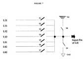
FIG. 7 , the inputs to the logic heads acquire the input signal through programmable switches S1-S7. In this example ofFIG. 7 , an input to a logic head (one from the group of IP1-IP5/Cinand Cin) originates from either one of its most adjacent neighboring logic heads or itself through one of three dedicated level zero lines (L01, L02 and L03) or from one of the level one lines (L11, L12, L13, . . . , L1n) or from one of level two lines (L21, . . . , L2m). For simplicity,FIG. 7 only shows three level one lines and one level two line. However, in other embodiments, fewer or greater lines for each level of interconnect is possible. - Pass switches S1-S7 are used to control to origination of an input to a logic head. To avoid signal contention or collision, only one switch S1-S9 is allowed to be programmed to the on position. When an input pin is unused, it is tied to either Vdd or Gnd using switches S8 or S9.
FIG. 6 illustrates alogic head 103 that can be selectively connected through programmable switches to four immediately adjacent logic heads by means of a level zerointerconnect 601. The logic head designated LH0 is at the center. Through dedicated lines, the outputs of LH0 (OP1-OP3) and the inputs to LH0 (IP1-IP5/Cinand Cin) can connect to its most adjacent neighbors to the east, to the north, to the south, and to the west, respectively. Those dedicated connections are implemented with three rings (one for each output signal OP1-OP3) surrounding each logic head. Each logic head's output has its own dedicated ring. Each ring is then connected to various inputs in the neighboring logic heads.- As noted above,
FIG. 1 illustrates an array of logic heads103 that can be selectively connected through programmable switches to other logic heads by means of a level one interconnect105. The level one interconnect network is generally used when a connection is needed that is beyond the most immediate neighbors. In one embodiment, the level one interconnect network is generally used when switch time delay is between 3 and 5 units inclusive. A connection point and a conventional routing switch causes one switch time unit delay each. However, a crossover switch (seen inFIG. 2 ) generates two switch time unit delays. FIG. 8 illustrates logic heads103 that can be selectively connected through programmable switches to distant logic heads by means of a level twointerconnect 801. In general, the level twointerconnect 801 is for transmitting signals between logic heads that are relatively far apart. The level twointerconnect 801 minimizes the amount of time delay, since switches are farther apart and fewer switches are traversed relative to the amount of distance traveled.FIG. 10 shows in greater detail the connections of a logic head to the level twointerconnect 801. Note that the inputs to the logic head can come from all directions, and not just from one direction.FIG. 2 illustrates acrossover switch 201 that can be used in the interconnect structures. For example the crossover switch of the present invention may be used in the level one interconnect ofFIG. 1 and are shown byreference numerals 201. Thecrossover switch 201 consists of eight pass transistors S1-S8. In addition, the crossover switch is shown operating on three vertical lines VT1-VT3 intersecting with three horizontal lines HT1-HT3. The crossover switch can be adapted to work with a greater or lesser number of intersecting signal lines.- When a downward signal on VT2 needs to cross over to a parallel track, i.e., VT1 or VT3, switches S3 and S8 or S3 and S4 are programmed to be on. Alternatively, when it is desired to route the signal to HT1 or HT3, switches S3 and S2 or S3 and S6 are programmed to be on. Further, when it is desired to route the signal onto HT2 going left, switches S3 and S1 are programmed to be on. Finally, when it is desired to route the signal onto HT2 right, switches S3 and S5 are programmed to be on. Thus, as can be seen, using the cross over switch of
FIG. 2 , any signal traveling on any line can be routed onto another line by selectively programming the switches S1-S8. Since acrossover switch 201 is physically symmetrical in all directions, no matter where an incoming signal originates, it can be switched to any other line. Every connection costs two switch time unit delays. - Examining the crossover switch of
FIG. 2 in greater detail, it can be seen that each line VT1-VT3 and HT1-HT3 can be switched into and out of a central “island node”203. For example, VT1 is connected to theisland node 203 by switch S8, VT3 is connected to the island node through switch S4, HT1 is connected to theisland node 203 by switch S2, HT3 is connected to the island node through switch S6, VT2 is connected to theisland node 203 by switches S3 and S7, and HT2 is connected to theisland node 203 by switches S1 and S5. The general concept is that each line should be able to access theisland node 203. Thus, although three vertical and three horizontal lines are shown inFIG. 2 , thecrossover switch 201 can be modified to have more or less lines. - It should be noted that the programmable switches discussed above can be implemented as conventional transistor switches, or in the alternative, use switches and programmable nonvolatile memory formed in accordance with pending U.S. patent application Ser. No. 09/955,641 filed Sep. 18, 2001 entitled “SEMICONDUCTOR MEMORY CELL AND MEMORY ARRAY USING A BREAKDOWN PHENOMENA IN AN ULTRA-THIN DIELECTRIC”, U.S. patent application Ser. No. 10/024,327 filed Dec. 17, 2001 entitled “SEMICONDUCTOR MEMORY CELL AND MEMORY ARRAY USING A BREAKDOWN PHENOMENA IN AN ULTRA-THIN DIELECTRIC”, and U.S. patent application Ser. No. 10/133,704 filed Apr. 26, 2002 entitled “HIGH DENSITY SEMICONDUCTOR MEMORY CELL AND MEMORY ARRAY USING A SINGLE TRANSISTOR”, assigned to the assignee of the present invention and which are herein incorporated by reference in their entirety.
- From the foregoing, it will be appreciated that specific embodiments of the invention have been described herein for purposes of illustration, but that various modifications may be made without deviating from the spirit and scope of the invention. Accordingly, the invention is not limited except as by the appended claims.
Claims (20)
Priority Applications (7)
| Application Number | Priority Date | Filing Date | Title |
|---|---|---|---|
| US10/642,370US6924664B2 (en) | 2003-08-15 | 2003-08-15 | Field programmable gate array |
| TW093124199ATWI326531B (en) | 2003-08-15 | 2004-08-12 | Field programmable gate array |
| JP2004234997AJP4565067B2 (en) | 2003-08-15 | 2004-08-12 | Field programmable gate array |
| EP04254857AEP1521368A3 (en) | 2003-08-15 | 2004-08-12 | Field programmable gate array |
| CNB2004100577566ACN100474776C (en) | 2003-08-15 | 2004-08-16 | Field programmable gate array |
| US11/109,966US6977521B2 (en) | 2003-08-15 | 2005-04-19 | Field programmable gate array |
| US11/252,126US7061275B2 (en) | 2003-08-15 | 2005-10-17 | Field programmable gate array |
Applications Claiming Priority (1)
| Application Number | Priority Date | Filing Date | Title |
|---|---|---|---|
| US10/642,370US6924664B2 (en) | 2003-08-15 | 2003-08-15 | Field programmable gate array |
Related Child Applications (1)
| Application Number | Title | Priority Date | Filing Date |
|---|---|---|---|
| US11/109,966DivisionUS6977521B2 (en) | 2003-08-15 | 2005-04-19 | Field programmable gate array |
Publications (2)
| Publication Number | Publication Date |
|---|---|
| US20050035783A1true US20050035783A1 (en) | 2005-02-17 |
| US6924664B2 US6924664B2 (en) | 2005-08-02 |
Family
ID=34136546
Family Applications (3)
| Application Number | Title | Priority Date | Filing Date |
|---|---|---|---|
| US10/642,370Expired - LifetimeUS6924664B2 (en) | 2003-08-15 | 2003-08-15 | Field programmable gate array |
| US11/109,966Expired - LifetimeUS6977521B2 (en) | 2003-08-15 | 2005-04-19 | Field programmable gate array |
| US11/252,126Expired - LifetimeUS7061275B2 (en) | 2003-08-15 | 2005-10-17 | Field programmable gate array |
Family Applications After (2)
| Application Number | Title | Priority Date | Filing Date |
|---|---|---|---|
| US11/109,966Expired - LifetimeUS6977521B2 (en) | 2003-08-15 | 2005-04-19 | Field programmable gate array |
| US11/252,126Expired - LifetimeUS7061275B2 (en) | 2003-08-15 | 2005-10-17 | Field programmable gate array |
Country Status (5)
| Country | Link |
|---|---|
| US (3) | US6924664B2 (en) |
| EP (1) | EP1521368A3 (en) |
| JP (1) | JP4565067B2 (en) |
| CN (1) | CN100474776C (en) |
| TW (1) | TWI326531B (en) |
Cited By (8)
| Publication number | Priority date | Publication date | Assignee | Title |
|---|---|---|---|---|
| US20030174723A1 (en)* | 2002-02-01 | 2003-09-18 | California Institute Of Technology | Fast router and hardware-assisted fast routing method |
| US20050063373A1 (en)* | 2003-07-24 | 2005-03-24 | Dehon Andre | Method and apparatus for network with multilayer metalization |
| US20070176644A1 (en)* | 2006-01-27 | 2007-08-02 | Klp International Ltd. | Programmable logic function generator using non-volatile programmable memory switches |
| US20070214445A1 (en)* | 2002-08-21 | 2007-09-13 | California Institute Of Technology | Element placement method and apparatus |
| WO2013181664A1 (en)* | 2012-06-01 | 2013-12-05 | The Regents Of The University Of California | Programmable logic circuit architecture using resistive memory elements |
| US20170331480A1 (en)* | 2015-01-21 | 2017-11-16 | Nec Corporation | Reconfigurable circuit |
| US9966121B2 (en) | 2016-06-14 | 2018-05-08 | SK Hynix Inc. | Comparison circuits and semiconductor devices employing the same |
| US20230119051A1 (en)* | 2020-09-14 | 2023-04-20 | SHENZHEN PANGO MICROSYSTEMS Co.,Ltd. | Method and apparatus for constructing fpga chip top-level schematic and storage medium |
Families Citing this family (13)
| Publication number | Priority date | Publication date | Assignee | Title |
|---|---|---|---|---|
| JP4368722B2 (en)* | 2004-03-31 | 2009-11-18 | Necエレクトロニクス株式会社 | Semiconductor device with general-purpose logic cell |
| US8114719B2 (en)* | 2004-06-03 | 2012-02-14 | Semiconductor Energy Laboratory Co., Ltd. | Memory device and manufacturing method of the same |
| JP4471776B2 (en)* | 2004-08-16 | 2010-06-02 | Necエレクトロニクス株式会社 | Semiconductor device and method for manufacturing semiconductor device |
| CN100433697C (en)* | 2006-06-01 | 2008-11-12 | 东南大学 | Multi-channel high-speed data processor and processing method |
| US8384155B2 (en)* | 2006-07-18 | 2013-02-26 | Ememory Technology Inc. | Semiconductor capacitor |
| US20080017917A1 (en)* | 2006-07-18 | 2008-01-24 | Ememory Technology Inc. | Non-volatile memory and fabricating method thereof |
| CN100449481C (en)* | 2007-06-29 | 2009-01-07 | 东南大学 | Storage control circuit with multiple-passage instruction pre-fetching function |
| US8692310B2 (en) | 2009-02-09 | 2014-04-08 | Spansion Llc | Gate fringing effect based channel formation for semiconductor device |
| US8208312B1 (en) | 2009-09-22 | 2012-06-26 | Novocell Semiconductor, Inc. | Non-volatile memory element integratable with standard CMOS circuitry |
| US8134859B1 (en) | 2009-09-25 | 2012-03-13 | Novocell Semiconductor, Inc. | Method of sensing a programmable non-volatile memory element |
| US8199590B1 (en) | 2009-09-25 | 2012-06-12 | Novocell Semiconductor, Inc. | Multiple time programmable non-volatile memory element |
| FR2979739A1 (en)* | 2011-09-07 | 2013-03-08 | Commissariat Energie Atomique | Switching device for programmable logic circuit i.e. field programmable gate array circuit, has switching units arranged between conductive elements and floating terminal and connecting or disconnecting elements to floating terminal |
| US9793897B1 (en)* | 2016-08-30 | 2017-10-17 | Instituto Potosino de Investigación Científica y Tecnológica A.C. | Method and circuit for integrating a programmable matrix in the field of reconfigurable logic gates employing a non-lineal system and an efficient programmable rewiring |
Citations (65)
| Publication number | Priority date | Publication date | Assignee | Title |
|---|---|---|---|---|
| US3634929A (en)* | 1968-11-02 | 1972-01-18 | Tokyo Shibaura Electric Co | Method of manufacturing semiconductor integrated circuits |
| US4322822A (en)* | 1979-01-02 | 1982-03-30 | Mcpherson Roger K | High density VMOS electrically programmable ROM |
| US4488262A (en)* | 1981-06-25 | 1984-12-11 | International Business Machines Corporation | Electronically programmable read only memory |
| US4490900A (en)* | 1982-01-29 | 1985-01-01 | Seeq Technology, Inc. | Method of fabricating an MOS memory array having electrically-programmable and electrically-erasable storage devices incorporated therein |
| US4502208A (en)* | 1979-01-02 | 1985-03-05 | Texas Instruments Incorporated | Method of making high density VMOS electrically-programmable ROM |
| US4507757A (en)* | 1982-03-23 | 1985-03-26 | Texas Instruments Incorporated | Avalanche fuse element in programmable memory |
| US4543594A (en)* | 1982-09-07 | 1985-09-24 | Intel Corporation | Fusible link employing capacitor structure |
| US4546273A (en)* | 1983-01-11 | 1985-10-08 | Burroughs Corporation | Dynamic re-programmable PLA |
| US4599705A (en)* | 1979-12-13 | 1986-07-08 | Energy Conversion Devices, Inc. | Programmable cell for use in programmable electronic arrays |
| US4613886A (en)* | 1981-07-09 | 1986-09-23 | Intel Corporation | CMOS static memory cell |
| US4677742A (en)* | 1983-01-18 | 1987-07-07 | Energy Conversion Devices, Inc. | Electronic matrix arrays and method for making the same |
| US4758986A (en)* | 1987-02-20 | 1988-07-19 | Motorola, Inc. | Single transistor cell for electrically-erasable programmable read-only memory and array thereof |
| US4794562A (en)* | 1986-09-29 | 1988-12-27 | Kabushiki Kaisha Toshiba | Electrically-erasable/programmable nonvolatile semiconductor memory device |
| US4823181A (en)* | 1986-05-09 | 1989-04-18 | Actel Corporation | Programmable low impedance anti-fuse element |
| US4876220A (en)* | 1986-05-16 | 1989-10-24 | Actel Corporation | Method of making programmable low impedance interconnect diode element |
| US4899205A (en)* | 1986-05-09 | 1990-02-06 | Actel Corporation | Electrically-programmable low-impedance anti-fuse element |
| US4943538A (en)* | 1986-05-09 | 1990-07-24 | Actel Corporation | Programmable low impedance anti-fuse element |
| US4962342A (en)* | 1989-05-04 | 1990-10-09 | Synaptics, Inc. | Dynamic synapse for neural network |
| US5138410A (en)* | 1989-12-11 | 1992-08-11 | Kabushiki Kaisha Toshiba | Nonvolatile semiconductor memory device having tunnel insulating film structure |
| US5150179A (en)* | 1990-07-05 | 1992-09-22 | Texas Instruments Incorporated | Diffusionless source/drain conductor electrically-erasable, electrically-programmable read-only memory and method for making and using the same |
| US5303185A (en)* | 1988-02-05 | 1994-04-12 | Emanuel Hazani | EEPROM cell structure and architecture with increased capacitance and with programming and erase terminals shared between several cells |
| US5304871A (en)* | 1992-07-24 | 1994-04-19 | Actel Corporation | Programmable interconnect architecture employing leaky programmable elements |
| US5323342A (en)* | 1991-10-31 | 1994-06-21 | Nippon Steel Corporation | MOS memory device |
| US5412244A (en)* | 1986-05-09 | 1995-05-02 | Actel Corporation | Electrically-programmable low-impedance anti-fuse element |
| US5455525A (en)* | 1993-12-06 | 1995-10-03 | Intelligent Logic Systems, Inc. | Hierarchically-structured programmable logic array and system for interconnecting logic elements in the logic array |
| US5477499A (en)* | 1993-10-13 | 1995-12-19 | Advanced Micro Devices, Inc. | Memory architecture for a three volt flash EEPROM |
| US5496756A (en)* | 1994-04-29 | 1996-03-05 | Motorola Inc. | Method for forming a nonvolatile memory device |
| US5576568A (en)* | 1995-01-18 | 1996-11-19 | Actel Corporation | Single-transistor electrically-alterable switch employing fowler nordheim tunneling for program and erase |
| US5578848A (en)* | 1994-05-04 | 1996-11-26 | Regents Of The University Of Texas System | Ultra thin dielectric for electronic devices and method of making same |
| US5586270A (en)* | 1993-09-30 | 1996-12-17 | Intel Corporation | Method and apparatus for upgrading a central processing unit and existing memory structure in a computer system |
| US5587603A (en)* | 1995-01-06 | 1996-12-24 | Actel Corporation | Two-transistor zero-power electrically-alterable non-volatile latch |
| US5600265A (en)* | 1986-09-19 | 1997-02-04 | Actel Corporation | Programmable interconnect architecture |
| US5675541A (en)* | 1992-03-25 | 1997-10-07 | U.S. Philips Corporation | Device comprising means for validating data written in a memory |
| US5675547A (en)* | 1995-06-01 | 1997-10-07 | Sony Corporation | One time programmable read only memory programmed by destruction of insulating layer |
| US5745417A (en)* | 1992-04-07 | 1998-04-28 | Mitsubishi Denki Kabushiki Kaisha | Electrically programmable and erasable nonvolatile semiconductor memory device and operating method therefor |
| US5781032A (en)* | 1996-09-09 | 1998-07-14 | International Business Machines Corporation | Programmable inverter circuit used in a programmable logic cell |
| US5825201A (en)* | 1996-06-21 | 1998-10-20 | Quicklogic Corporation | Programming architecture for a programmable integrated circuit employing antifuses |
| US5880512A (en)* | 1991-04-26 | 1999-03-09 | Quicklogic Corporation | Programmable interconnect structures and programmable integrated circuits |
| US5889411A (en)* | 1997-02-26 | 1999-03-30 | Xilinx, Inc. | FPGA having logic element carry chains capable of generating wide XOR functions |
| US5909049A (en)* | 1997-02-11 | 1999-06-01 | Actel Corporation | Antifuse programmed PROM cell |
| US5986931A (en)* | 1997-01-02 | 1999-11-16 | Caywood; John M. | Low voltage single CMOS electrically erasable read-only memory |
| US5986939A (en)* | 1997-12-24 | 1999-11-16 | Sanyo Electric Co., Ltd. | Non-volatile semiconductor memory device |
| US6016268A (en)* | 1997-02-18 | 2000-01-18 | Richard Mann | Three transistor multi-state dynamic memory cell for embedded CMOS logic applications |
| US6034893A (en)* | 1999-06-15 | 2000-03-07 | Vantis Corporation | Non-volatile memory cell having dual avalanche injection elements |
| US6040968A (en)* | 1997-06-30 | 2000-03-21 | Texas Instruments Incorporated | EOS/ESD protection for high density integrated circuits |
| US6064595A (en)* | 1998-12-23 | 2000-05-16 | Vantis Corporation | Floating gate memory apparatus and method for selected programming thereof |
| US6064225A (en)* | 1998-03-20 | 2000-05-16 | Lucent Technologies Inc. | Global signal distribution with reduced routing tracks in an FPGA |
| US6157568A (en)* | 1998-12-23 | 2000-12-05 | Vantis Corporation | Avalanche programmed floating gate memory cell structure with program element in first polysilicon layer |
| US6166954A (en)* | 1999-07-14 | 2000-12-26 | Programmable Microelectronics Corporation | Single poly non-volatile memory having a PMOS write path and an NMOS read path |
| US6214666B1 (en)* | 1998-12-18 | 2001-04-10 | Vantis Corporation | Method of forming a non-volatile memory device |
| US6215140B1 (en)* | 1998-09-18 | 2001-04-10 | Siemens Aktiengesellschaft | Electrically programmable non-volatile memory cell configuration |
| US6218274B1 (en)* | 1997-10-28 | 2001-04-17 | Sony Corporation | Semiconductor device and manufacturing method thereof |
| US6232631B1 (en)* | 1998-12-21 | 2001-05-15 | Vantis Corporation | Floating gate memory cell structure with programming mechanism outside the read path |
| US20010003374A1 (en)* | 1999-12-09 | 2001-06-14 | U.S. Philips Corporation | Semiconductor device comprising a security coating and smartcard provided with such a device |
| US6249809B1 (en)* | 1993-08-30 | 2001-06-19 | William L. Bro | Automated and interactive telecommunications system |
| US6282123B1 (en)* | 1998-12-21 | 2001-08-28 | Lattice Semiconductor Corporation | Method of fabricating, programming, and erasing a dual pocket two sided program/erase non-volatile memory cell |
| US6294809B1 (en)* | 1998-12-28 | 2001-09-25 | Vantis Corporation | Avalanche programmed floating gate memory cell structure with program element in polysilicon |
| US6297103B1 (en)* | 2000-02-28 | 2001-10-02 | Micron Technology, Inc. | Structure and method for dual gate oxide thicknesses |
| US6304666B1 (en)* | 1998-10-07 | 2001-10-16 | The United States Of America As Represented By The United States Department Of Energy | Apparatus for sensing patterns of electrical field variations across a surface |
| US6351428B2 (en)* | 2000-02-29 | 2002-02-26 | Micron Technology, Inc. | Programmable low voltage decode circuits with ultra-thin tunnel oxides |
| US6421293B1 (en)* | 1998-12-23 | 2002-07-16 | Stmicroelectronics S.A. | One-time programmable memory cell in CMOS technology |
| US6431456B2 (en)* | 1999-12-03 | 2002-08-13 | Hitachi, Ltd. | IC card |
| US6456535B2 (en)* | 2000-02-28 | 2002-09-24 | Micron Technology, Inc. | Dynamic flash memory cells with ultra thin tunnel oxides |
| US6515509B1 (en)* | 2000-07-13 | 2003-02-04 | Xilinx, Inc. | Programmable logic device structures in standard cell devices |
| US6556481B1 (en)* | 2001-02-21 | 2003-04-29 | Aplus Flash Technology, Inc. | 3-step write operation nonvolatile semiconductor one-transistor, nor-type flash EEPROM memory cell |
Family Cites Families (46)
| Publication number | Priority date | Publication date | Assignee | Title |
|---|---|---|---|---|
| US4870302A (en) | 1984-03-12 | 1989-09-26 | Xilinx, Inc. | Configurable electrical circuit having configurable logic elements and configurable interconnects |
| US4670749A (en)* | 1984-04-13 | 1987-06-02 | Zilog, Inc. | Integrated circuit programmable cross-point connection technique |
| JPS61292295A (en) | 1985-06-19 | 1986-12-23 | Fujitsu Ltd | Programmable read-only memory and its writing method |
| US4758745B1 (en) | 1986-09-19 | 1994-11-15 | Actel Corp | User programmable integrated circuit interconnect architecture and test method |
| DE3635687A1 (en)* | 1986-10-21 | 1988-05-05 | Messerschmitt Boelkow Blohm | IMAGE SENSOR |
| JP2688492B2 (en) | 1987-06-19 | 1997-12-10 | アドバンスト・マイクロ・デバイシズ・インコーポレイテッド | Electrically erasable programmable read-only memory |
| US5268319A (en) | 1988-06-08 | 1993-12-07 | Eliyahou Harari | Highly compact EPROM and flash EEPROM devices |
| US5311080A (en)* | 1993-03-26 | 1994-05-10 | At&T Bell Laboratories | Field programmable gate array with direct input/output connection |
| US5444404A (en)* | 1994-03-03 | 1995-08-22 | Vlsi Technology, Inc. | Scan flip-flop with power saving feature |
| US5650336A (en) | 1994-09-19 | 1997-07-22 | Matsushita Electric Industrial Co., Ltd. | Method of presuming life time of semiconductor device |
| US5600264A (en)* | 1995-10-16 | 1997-02-04 | Xilinx, Inc. | Programmable single buffered six pass transistor configuration |
| JPH09307428A (en)* | 1996-05-14 | 1997-11-28 | Hitachi Ltd | Variable logic integrated circuit |
| US5784636A (en) | 1996-05-28 | 1998-07-21 | National Semiconductor Corporation | Reconfigurable computer architecture for use in signal processing applications |
| US5892962A (en) | 1996-11-12 | 1999-04-06 | Lucent Technologies Inc. | FPGA-based processor |
| US5889413A (en)* | 1996-11-22 | 1999-03-30 | Xilinx, Inc. | Lookup tables which double as shift registers |
| TW417256B (en) | 1997-01-31 | 2001-01-01 | Seiko Epson Corp | Semiconductor MOS device and its manufacturing method |
| US5949712A (en)* | 1997-03-27 | 1999-09-07 | Xilinx, Inc. | Non-volatile memory array using gate breakdown structure |
| US6077719A (en) | 1997-07-24 | 2000-06-20 | Matsushita Electronics Corporation | Semiconductor device evaluation method, method of controlling the semiconductor device production processes and recording medium |
| JPH11135512A (en) | 1997-10-31 | 1999-05-21 | Mitsubishi Electric Corp | Power semiconductor device and method of manufacturing the same |
| US6047243A (en) | 1997-12-11 | 2000-04-04 | Advanced Micro Devices, Inc. | Method for quantifying ultra-thin dielectric reliability: time dependent dielectric wear-out |
| IT1298816B1 (en) | 1998-03-27 | 2000-02-02 | Sgs Thomson Microelectronics | SWITCHING CIRCUIT WITH VARIABLE OUTPUT VOLTAGE BETWEEN A REFERENCE VOLTAGE AND A NEGATIVE VOLTAGE |
| JP3611714B2 (en)* | 1998-04-08 | 2005-01-19 | 株式会社ルネサステクノロジ | Processor |
| US6198652B1 (en) | 1998-04-13 | 2001-03-06 | Kabushiki Kaisha Toshiba | Non-volatile semiconductor integrated memory device |
| JP3123977B2 (en)* | 1998-06-04 | 2001-01-15 | 日本電気株式会社 | Programmable function block |
| US6177830B1 (en)* | 1999-03-05 | 2001-01-23 | Xilinx, Inc | High voltage charge pump using standard sub 0.35 micron CMOS process |
| US6055205A (en)* | 1999-03-05 | 2000-04-25 | Xilinx, Inc. | Decoder for a non-volatile memory array using gate breakdown structure in standard sub 0.35 micron CMOS process |
| US6044012A (en)* | 1999-03-05 | 2000-03-28 | Xilinx, Inc. | Non-volatile memory array using gate breakdown structure in standard sub 0.35 micron CMOS process |
| US6236229B1 (en) | 1999-05-13 | 2001-05-22 | Easic Corporation | Integrated circuits which employ look up tables to provide highly efficient logic cells and logic functionalities |
| US6153463A (en) | 1999-07-09 | 2000-11-28 | Macronix International Co., Ltd. | Triple plate capacitor and method for manufacturing |
| US6678646B1 (en) | 1999-12-14 | 2004-01-13 | Atmel Corporation | Method for implementing a physical design for a dynamically reconfigurable logic circuit |
| US6272047B1 (en) | 1999-12-17 | 2001-08-07 | Micron Technology, Inc. | Flash memory cell |
| US6459634B1 (en) | 2000-01-31 | 2002-10-01 | Micron Technology, Inc. | Circuits and methods for testing memory cells along a periphery of a memory array |
| US6910069B1 (en)* | 2000-07-31 | 2005-06-21 | The Boeing Company | Joining a broadcast channel |
| US6476636B1 (en) | 2000-09-02 | 2002-11-05 | Actel Corporation | Tileable field-programmable gate array architecture |
| JP2002217709A (en)* | 2001-01-22 | 2002-08-02 | Sharp Corp | Programmable logic circuit |
| KR100421040B1 (en) | 2001-05-07 | 2004-03-03 | 삼성전자주식회사 | A semiconductor memory cell for reducing power consumption and data output time using controllable virtual ground |
| JP3613396B2 (en)* | 2001-06-25 | 2005-01-26 | 日本電気株式会社 | Function block |
| US6602729B2 (en) | 2001-07-13 | 2003-08-05 | Infineon Technologies Ag | Pulse voltage breakdown (VBD) technique for inline gate oxide reliability monitoring |
| US6633182B2 (en) | 2001-09-05 | 2003-10-14 | Carnegie Mellon University | Programmable gate array based on configurable metal interconnect vias |
| US6700151B2 (en) | 2001-10-17 | 2004-03-02 | Kilopass Technologies, Inc. | Reprogrammable non-volatile memory using a breakdown phenomena in an ultra-thin dielectric |
| US6754881B2 (en) | 2001-12-10 | 2004-06-22 | International Business Machines Corporation | Field programmable network processor and method for customizing a network processor |
| JP2003257178A (en) | 2002-03-06 | 2003-09-12 | Matsushita Electric Ind Co Ltd | Semiconductor memory device |
| US6777757B2 (en) | 2002-04-26 | 2004-08-17 | Kilopass Technologies, Inc. | High density semiconductor memory cell and memory array using a single transistor |
| US6753590B2 (en) | 2002-07-08 | 2004-06-22 | International Business Machines Corporation | High impedance antifuse |
| US6650143B1 (en) | 2002-07-08 | 2003-11-18 | Kilopass Technologies, Inc. | Field programmable gate array based upon transistor gate oxide breakdown |
| US6753390B2 (en)* | 2002-09-04 | 2004-06-22 | Univation Technologies, Llc | Gas phase polymerization process |
- 2003
- 2003-08-15USUS10/642,370patent/US6924664B2/ennot_activeExpired - Lifetime
- 2004
- 2004-08-12JPJP2004234997Apatent/JP4565067B2/ennot_activeExpired - Lifetime
- 2004-08-12EPEP04254857Apatent/EP1521368A3/ennot_activeWithdrawn
- 2004-08-12TWTW093124199Apatent/TWI326531B/ennot_activeIP Right Cessation
- 2004-08-16CNCNB2004100577566Apatent/CN100474776C/ennot_activeExpired - Lifetime
- 2005
- 2005-04-19USUS11/109,966patent/US6977521B2/ennot_activeExpired - Lifetime
- 2005-10-17USUS11/252,126patent/US7061275B2/ennot_activeExpired - Lifetime
Patent Citations (69)
| Publication number | Priority date | Publication date | Assignee | Title |
|---|---|---|---|---|
| US3634929A (en)* | 1968-11-02 | 1972-01-18 | Tokyo Shibaura Electric Co | Method of manufacturing semiconductor integrated circuits |
| US4322822A (en)* | 1979-01-02 | 1982-03-30 | Mcpherson Roger K | High density VMOS electrically programmable ROM |
| US4502208A (en)* | 1979-01-02 | 1985-03-05 | Texas Instruments Incorporated | Method of making high density VMOS electrically-programmable ROM |
| US4599705A (en)* | 1979-12-13 | 1986-07-08 | Energy Conversion Devices, Inc. | Programmable cell for use in programmable electronic arrays |
| US4488262A (en)* | 1981-06-25 | 1984-12-11 | International Business Machines Corporation | Electronically programmable read only memory |
| US4613886A (en)* | 1981-07-09 | 1986-09-23 | Intel Corporation | CMOS static memory cell |
| US4490900A (en)* | 1982-01-29 | 1985-01-01 | Seeq Technology, Inc. | Method of fabricating an MOS memory array having electrically-programmable and electrically-erasable storage devices incorporated therein |
| US4507757A (en)* | 1982-03-23 | 1985-03-26 | Texas Instruments Incorporated | Avalanche fuse element in programmable memory |
| US4543594A (en)* | 1982-09-07 | 1985-09-24 | Intel Corporation | Fusible link employing capacitor structure |
| US4546273A (en)* | 1983-01-11 | 1985-10-08 | Burroughs Corporation | Dynamic re-programmable PLA |
| US4677742A (en)* | 1983-01-18 | 1987-07-07 | Energy Conversion Devices, Inc. | Electronic matrix arrays and method for making the same |
| US4899205A (en)* | 1986-05-09 | 1990-02-06 | Actel Corporation | Electrically-programmable low-impedance anti-fuse element |
| US5412244A (en)* | 1986-05-09 | 1995-05-02 | Actel Corporation | Electrically-programmable low-impedance anti-fuse element |
| US4823181A (en)* | 1986-05-09 | 1989-04-18 | Actel Corporation | Programmable low impedance anti-fuse element |
| US4943538A (en)* | 1986-05-09 | 1990-07-24 | Actel Corporation | Programmable low impedance anti-fuse element |
| US4876220A (en)* | 1986-05-16 | 1989-10-24 | Actel Corporation | Method of making programmable low impedance interconnect diode element |
| US5600265A (en)* | 1986-09-19 | 1997-02-04 | Actel Corporation | Programmable interconnect architecture |
| US4794562A (en)* | 1986-09-29 | 1988-12-27 | Kabushiki Kaisha Toshiba | Electrically-erasable/programmable nonvolatile semiconductor memory device |
| US4758986A (en)* | 1987-02-20 | 1988-07-19 | Motorola, Inc. | Single transistor cell for electrically-erasable programmable read-only memory and array thereof |
| US5303185A (en)* | 1988-02-05 | 1994-04-12 | Emanuel Hazani | EEPROM cell structure and architecture with increased capacitance and with programming and erase terminals shared between several cells |
| US4962342A (en)* | 1989-05-04 | 1990-10-09 | Synaptics, Inc. | Dynamic synapse for neural network |
| US4962342B1 (en)* | 1989-05-04 | 1992-09-15 | Synaptics Inc | |
| US5138410A (en)* | 1989-12-11 | 1992-08-11 | Kabushiki Kaisha Toshiba | Nonvolatile semiconductor memory device having tunnel insulating film structure |
| US5150179A (en)* | 1990-07-05 | 1992-09-22 | Texas Instruments Incorporated | Diffusionless source/drain conductor electrically-erasable, electrically-programmable read-only memory and method for making and using the same |
| US6097077A (en)* | 1991-04-26 | 2000-08-01 | Quicklogic Corporation | Programmable interconnect structures and programmable integrated circuits |
| US5880512A (en)* | 1991-04-26 | 1999-03-09 | Quicklogic Corporation | Programmable interconnect structures and programmable integrated circuits |
| US5323342A (en)* | 1991-10-31 | 1994-06-21 | Nippon Steel Corporation | MOS memory device |
| US5675541A (en)* | 1992-03-25 | 1997-10-07 | U.S. Philips Corporation | Device comprising means for validating data written in a memory |
| US5745417A (en)* | 1992-04-07 | 1998-04-28 | Mitsubishi Denki Kabushiki Kaisha | Electrically programmable and erasable nonvolatile semiconductor memory device and operating method therefor |
| US5304871A (en)* | 1992-07-24 | 1994-04-19 | Actel Corporation | Programmable interconnect architecture employing leaky programmable elements |
| US6249809B1 (en)* | 1993-08-30 | 2001-06-19 | William L. Bro | Automated and interactive telecommunications system |
| US5586270A (en)* | 1993-09-30 | 1996-12-17 | Intel Corporation | Method and apparatus for upgrading a central processing unit and existing memory structure in a computer system |
| US5477499A (en)* | 1993-10-13 | 1995-12-19 | Advanced Micro Devices, Inc. | Memory architecture for a three volt flash EEPROM |
| US5455525A (en)* | 1993-12-06 | 1995-10-03 | Intelligent Logic Systems, Inc. | Hierarchically-structured programmable logic array and system for interconnecting logic elements in the logic array |
| US5496756A (en)* | 1994-04-29 | 1996-03-05 | Motorola Inc. | Method for forming a nonvolatile memory device |
| US5578848A (en)* | 1994-05-04 | 1996-11-26 | Regents Of The University Of Texas System | Ultra thin dielectric for electronic devices and method of making same |
| US5587603A (en)* | 1995-01-06 | 1996-12-24 | Actel Corporation | Two-transistor zero-power electrically-alterable non-volatile latch |
| US5576568A (en)* | 1995-01-18 | 1996-11-19 | Actel Corporation | Single-transistor electrically-alterable switch employing fowler nordheim tunneling for program and erase |
| US5675547A (en)* | 1995-06-01 | 1997-10-07 | Sony Corporation | One time programmable read only memory programmed by destruction of insulating layer |
| US6084428A (en)* | 1996-06-21 | 2000-07-04 | Quicklogic Corporation | Programmable integrated circuit having shared programming conductors between columns of logic modules |
| US5825200A (en)* | 1996-06-21 | 1998-10-20 | Quicklogic Corporation | Programming architecture for a programmable integrated circuit employing antifuses |
| US5825201A (en)* | 1996-06-21 | 1998-10-20 | Quicklogic Corporation | Programming architecture for a programmable integrated circuit employing antifuses |
| US5781032A (en)* | 1996-09-09 | 1998-07-14 | International Business Machines Corporation | Programmable inverter circuit used in a programmable logic cell |
| US5986931A (en)* | 1997-01-02 | 1999-11-16 | Caywood; John M. | Low voltage single CMOS electrically erasable read-only memory |
| US5909049A (en)* | 1997-02-11 | 1999-06-01 | Actel Corporation | Antifuse programmed PROM cell |
| US6016268A (en)* | 1997-02-18 | 2000-01-18 | Richard Mann | Three transistor multi-state dynamic memory cell for embedded CMOS logic applications |
| US5889411A (en)* | 1997-02-26 | 1999-03-30 | Xilinx, Inc. | FPGA having logic element carry chains capable of generating wide XOR functions |
| US6040968A (en)* | 1997-06-30 | 2000-03-21 | Texas Instruments Incorporated | EOS/ESD protection for high density integrated circuits |
| US6218274B1 (en)* | 1997-10-28 | 2001-04-17 | Sony Corporation | Semiconductor device and manufacturing method thereof |
| US5986939A (en)* | 1997-12-24 | 1999-11-16 | Sanyo Electric Co., Ltd. | Non-volatile semiconductor memory device |
| US6064225A (en)* | 1998-03-20 | 2000-05-16 | Lucent Technologies Inc. | Global signal distribution with reduced routing tracks in an FPGA |
| US6215140B1 (en)* | 1998-09-18 | 2001-04-10 | Siemens Aktiengesellschaft | Electrically programmable non-volatile memory cell configuration |
| US6304666B1 (en)* | 1998-10-07 | 2001-10-16 | The United States Of America As Represented By The United States Department Of Energy | Apparatus for sensing patterns of electrical field variations across a surface |
| US6214666B1 (en)* | 1998-12-18 | 2001-04-10 | Vantis Corporation | Method of forming a non-volatile memory device |
| US6232631B1 (en)* | 1998-12-21 | 2001-05-15 | Vantis Corporation | Floating gate memory cell structure with programming mechanism outside the read path |
| US6282123B1 (en)* | 1998-12-21 | 2001-08-28 | Lattice Semiconductor Corporation | Method of fabricating, programming, and erasing a dual pocket two sided program/erase non-volatile memory cell |
| US6064595A (en)* | 1998-12-23 | 2000-05-16 | Vantis Corporation | Floating gate memory apparatus and method for selected programming thereof |
| US6157568A (en)* | 1998-12-23 | 2000-12-05 | Vantis Corporation | Avalanche programmed floating gate memory cell structure with program element in first polysilicon layer |
| US6421293B1 (en)* | 1998-12-23 | 2002-07-16 | Stmicroelectronics S.A. | One-time programmable memory cell in CMOS technology |
| US6294809B1 (en)* | 1998-12-28 | 2001-09-25 | Vantis Corporation | Avalanche programmed floating gate memory cell structure with program element in polysilicon |
| US6034893A (en)* | 1999-06-15 | 2000-03-07 | Vantis Corporation | Non-volatile memory cell having dual avalanche injection elements |
| US6166954A (en)* | 1999-07-14 | 2000-12-26 | Programmable Microelectronics Corporation | Single poly non-volatile memory having a PMOS write path and an NMOS read path |
| US6431456B2 (en)* | 1999-12-03 | 2002-08-13 | Hitachi, Ltd. | IC card |
| US20010003374A1 (en)* | 1999-12-09 | 2001-06-14 | U.S. Philips Corporation | Semiconductor device comprising a security coating and smartcard provided with such a device |
| US6297103B1 (en)* | 2000-02-28 | 2001-10-02 | Micron Technology, Inc. | Structure and method for dual gate oxide thicknesses |
| US6456535B2 (en)* | 2000-02-28 | 2002-09-24 | Micron Technology, Inc. | Dynamic flash memory cells with ultra thin tunnel oxides |
| US6351428B2 (en)* | 2000-02-29 | 2002-02-26 | Micron Technology, Inc. | Programmable low voltage decode circuits with ultra-thin tunnel oxides |
| US6515509B1 (en)* | 2000-07-13 | 2003-02-04 | Xilinx, Inc. | Programmable logic device structures in standard cell devices |
| US6556481B1 (en)* | 2001-02-21 | 2003-04-29 | Aplus Flash Technology, Inc. | 3-step write operation nonvolatile semiconductor one-transistor, nor-type flash EEPROM memory cell |
Cited By (13)
| Publication number | Priority date | Publication date | Assignee | Title |
|---|---|---|---|---|
| US7342414B2 (en) | 2002-02-01 | 2008-03-11 | California Institute Of Technology | Fast router and hardware-assisted fast routing method |
| US20030174723A1 (en)* | 2002-02-01 | 2003-09-18 | California Institute Of Technology | Fast router and hardware-assisted fast routing method |
| US20070214445A1 (en)* | 2002-08-21 | 2007-09-13 | California Institute Of Technology | Element placement method and apparatus |
| US20050063373A1 (en)* | 2003-07-24 | 2005-03-24 | Dehon Andre | Method and apparatus for network with multilayer metalization |
| US7285487B2 (en)* | 2003-07-24 | 2007-10-23 | California Institute Of Technology | Method and apparatus for network with multilayer metalization |
| US7411424B2 (en)* | 2006-01-27 | 2008-08-12 | Klp International, Ltd. | Programmable logic function generator using non-volatile programmable memory switches |
| US20070176644A1 (en)* | 2006-01-27 | 2007-08-02 | Klp International Ltd. | Programmable logic function generator using non-volatile programmable memory switches |
| WO2013181664A1 (en)* | 2012-06-01 | 2013-12-05 | The Regents Of The University Of California | Programmable logic circuit architecture using resistive memory elements |
| US9461649B2 (en) | 2012-06-01 | 2016-10-04 | The Regents Of The University Of California | Programmable logic circuit architecture using resistive memory elements |
| US20170331480A1 (en)* | 2015-01-21 | 2017-11-16 | Nec Corporation | Reconfigurable circuit |
| US10027326B2 (en)* | 2015-01-21 | 2018-07-17 | Nec Corporation | Reconfigurable circuit |
| US9966121B2 (en) | 2016-06-14 | 2018-05-08 | SK Hynix Inc. | Comparison circuits and semiconductor devices employing the same |
| US20230119051A1 (en)* | 2020-09-14 | 2023-04-20 | SHENZHEN PANGO MICROSYSTEMS Co.,Ltd. | Method and apparatus for constructing fpga chip top-level schematic and storage medium |
Also Published As
| Publication number | Publication date |
|---|---|
| US20060033528A1 (en) | 2006-02-16 |
| US20050184754A1 (en) | 2005-08-25 |
| US6977521B2 (en) | 2005-12-20 |
| EP1521368A2 (en) | 2005-04-06 |
| EP1521368A3 (en) | 2005-04-13 |
| CN100474776C (en) | 2009-04-01 |
| US6924664B2 (en) | 2005-08-02 |
| TWI326531B (en) | 2010-06-21 |
| JP4565067B2 (en) | 2010-10-20 |
| US7061275B2 (en) | 2006-06-13 |
| TW200518460A (en) | 2005-06-01 |
| CN1637671A (en) | 2005-07-13 |
| JP2005124151A (en) | 2005-05-12 |
Similar Documents
| Publication | Publication Date | Title |
|---|---|---|
| US6924664B2 (en) | Field programmable gate array | |
| US5280202A (en) | Programmable application specific integrated circuit and logic cell therefor | |
| US5430390A (en) | Programmable application specific integrated circuit and logic cell therefor | |
| US5450021A (en) | EPLD chip with hybrid architecture optimized for both speed and flexibility | |
| US6480025B1 (en) | Driver circuitry for programmable logic devices with hierarchical interconnection resources | |
| US6903573B1 (en) | Programmable logic device with enhanced wide input product term cascading | |
| US6392438B1 (en) | Programmable logic array integrated circuit devices | |
| US6359469B1 (en) | Logic element for a programmable logic integrated circuit | |
| US5760604A (en) | Interconnect architecture for field programmable gate array | |
| EP0712548B1 (en) | Architecture and interconnect scheme for programmable logic circuits | |
| US6501296B2 (en) | Logic/memory circuit having a plurality of operating modes | |
| US5416367A (en) | Programmable application specific integrated circuit and logic cell therefor | |
| US6268743B1 (en) | Block symmetrization in a field programmable gate array | |
| US5463328A (en) | Expanded programmable logic architecture | |
| US5714890A (en) | Programmable logic device with fixed and programmable memory | |
| US7557612B2 (en) | Block symmetrization in a field programmable gate array | |
| US6879184B1 (en) | Programmable logic device architecture based on arrays of LUT-based Boolean terms | |
| US6429681B1 (en) | Programmable logic device routing architecture to facilitate register re-timing | |
| US7425842B2 (en) | Logic basic cell | |
| US6861871B1 (en) | Cascaded logic block architecture for complex programmable logic devices | |
| US6922078B1 (en) | Programmable logic device with enhanced wide and deep logic capability |
Legal Events
| Date | Code | Title | Description |
|---|---|---|---|
| AS | Assignment | Owner name:KILOPASS TECHNOLOGIES, INC., CALIFORNIA Free format text:ASSIGNMENT OF ASSIGNORS INTEREST;ASSIGNOR:WANG, MAN;REEL/FRAME:014410/0023 Effective date:20030814 | |
| STCF | Information on status: patent grant | Free format text:PATENTED CASE | |
| CC | Certificate of correction | ||
| AS | Assignment | Owner name:KILOPASS TECHNOLOGY, INC., CALIFORNIA Free format text:ASSIGNMENT OF ASSIGNORS INTEREST;ASSIGNOR:WANG, MAN;REEL/FRAME:017937/0628 Effective date:20030814 | |
| AS | Assignment | Owner name:KLP INTERNATIONAL LTD., CALIFORNIA Free format text:ASSIGNMENT OF ASSIGNORS INTEREST;ASSIGNOR:KILOPASS TECHNOLOGY, INC.;REEL/FRAME:017945/0678 Effective date:20060713 | |
| FPAY | Fee payment | Year of fee payment:4 | |
| FEPP | Fee payment procedure | Free format text:PAYOR NUMBER ASSIGNED (ORIGINAL EVENT CODE: ASPN); ENTITY STATUS OF PATENT OWNER: LARGE ENTITY | |
| FEPP | Fee payment procedure | Free format text:PAT HOLDER NO LONGER CLAIMS SMALL ENTITY STATUS, ENTITY STATUS SET TO UNDISCOUNTED (ORIGINAL EVENT CODE: STOL); ENTITY STATUS OF PATENT OWNER: LARGE ENTITY | |
| AS | Assignment | Owner name:SILICONBLUE TECHNOLOGIES LTD., CAYMAN ISLANDS Free format text:CHANGE OF NAME;ASSIGNOR:KLP INTERNATIONAL LTD.;REEL/FRAME:027877/0708 Effective date:20071211 | |
| AS | Assignment | Owner name:LATTICE SEMICONDUCTOR LIMITED, BERMUDA Free format text:MERGER;ASSIGNOR:SILCONBLUE TECHNOLOGIES LTD.;REEL/FRAME:028011/0951 Effective date:20120402 | |
| FPAY | Fee payment | Year of fee payment:8 | |
| AS | Assignment | Owner name:LATTICE SEMICONDUCTOR CORPORATION, OREGON Free format text:ASSIGNMENT OF ASSIGNORS INTEREST;ASSIGNOR:LATTICE SEMICONDUCTOR LIMITED;REEL/FRAME:035101/0559 Effective date:20150306 | |
| AS | Assignment | Owner name:JEFFERIES FINANCE LLC, NEW YORK Free format text:SECURITY INTEREST;ASSIGNORS:LATTICE SEMICONDUCTOR CORPORATION;SIBEAM, INC.;SILICON IMAGE, INC.;AND OTHERS;REEL/FRAME:035222/0866 Effective date:20150310 | |
| FPAY | Fee payment | Year of fee payment:12 | |
| AS | Assignment | Owner name:SYNOPSYS, INC., CALIFORNIA Free format text:ASSIGNMENT OF ASSIGNORS INTEREST;ASSIGNOR:KILOPASS TECHNOLOGY, INC.;REEL/FRAME:046099/0269 Effective date:20180501 | |
| AS | Assignment | Owner name:LATTICE SEMICONDUCTOR CORPORATION, OREGON Free format text:RELEASE BY SECURED PARTY;ASSIGNOR:JEFFERIES FINANCE LLC;REEL/FRAME:049827/0326 Effective date:20190517 Owner name:SILICON IMAGE, INC., OREGON Free format text:RELEASE BY SECURED PARTY;ASSIGNOR:JEFFERIES FINANCE LLC;REEL/FRAME:049827/0326 Effective date:20190517 Owner name:DVDO, INC., OREGON Free format text:RELEASE BY SECURED PARTY;ASSIGNOR:JEFFERIES FINANCE LLC;REEL/FRAME:049827/0326 Effective date:20190517 Owner name:SIBEAM, INC., OREGON Free format text:RELEASE BY SECURED PARTY;ASSIGNOR:JEFFERIES FINANCE LLC;REEL/FRAME:049827/0326 Effective date:20190517 Owner name:WELLS FARGO BANK, NATIONAL ASSOCIATION, AS ADMINIS Free format text:SECURITY INTEREST;ASSIGNOR:LATTICE SEMICONDUCTOR CORPORATION;REEL/FRAME:049980/0786 Effective date:20190517 Owner name:WELLS FARGO BANK, NATIONAL ASSOCIATION, AS ADMINISTRATIVE AGENT, COLORADO Free format text:SECURITY INTEREST;ASSIGNOR:LATTICE SEMICONDUCTOR CORPORATION;REEL/FRAME:049980/0786 Effective date:20190517 |