US20050035410A1 - Semiconductor diode with reduced leakage - Google Patents
Semiconductor diode with reduced leakageDownload PDFInfo
- Publication number
- US20050035410A1 US20050035410A1US10/641,813US64181303AUS2005035410A1US 20050035410 A1US20050035410 A1US 20050035410A1US 64181303 AUS64181303 AUS 64181303AUS 2005035410 A1US2005035410 A1US 2005035410A1
- Authority
- US
- United States
- Prior art keywords
- gate electrode
- oxide
- diode
- dielectric
- silicide
- Prior art date
- Legal status (The legal status is an assumption and is not a legal conclusion. Google has not performed a legal analysis and makes no representation as to the accuracy of the status listed.)
- Abandoned
Links
- 239000004065semiconductorSubstances0.000titleclaimsdescription22
- XUIMIQQOPSSXEZ-UHFFFAOYSA-NSiliconChemical compound[Si]XUIMIQQOPSSXEZ-UHFFFAOYSA-N0.000claimsabstractdescription39
- 229910052710siliconInorganic materials0.000claimsabstractdescription39
- 239000010703siliconSubstances0.000claimsabstractdescription39
- 239000000758substrateSubstances0.000claimsabstractdescription37
- 239000012212insulatorSubstances0.000claimsabstractdescription28
- 210000000746body regionAnatomy0.000claimsabstractdescription18
- 238000000034methodMethods0.000claimsdescription53
- 229910021332silicideInorganic materials0.000claimsdescription34
- FVBUAEGBCNSCDD-UHFFFAOYSA-Nsilicide(4-)Chemical compound[Si-4]FVBUAEGBCNSCDD-UHFFFAOYSA-N0.000claimsdescription32
- 239000000463materialSubstances0.000claimsdescription29
- 239000002019doping agentSubstances0.000claimsdescription20
- 238000002955isolationMethods0.000claimsdescription19
- 229910052751metalInorganic materials0.000claimsdescription19
- 239000002184metalSubstances0.000claimsdescription19
- 229910052735hafniumInorganic materials0.000claimsdescription18
- VBJZVLUMGGDVMO-UHFFFAOYSA-Nhafnium atomChemical compound[Hf]VBJZVLUMGGDVMO-UHFFFAOYSA-N0.000claimsdescription18
- 125000006850spacer groupChemical group0.000claimsdescription15
- VYPSYNLAJGMNEJ-UHFFFAOYSA-NSilicium dioxideChemical groupO=[Si]=OVYPSYNLAJGMNEJ-UHFFFAOYSA-N0.000claimsdescription14
- 229910052814silicon oxideInorganic materials0.000claimsdescription14
- BASFCYQUMIYNBI-UHFFFAOYSA-NplatinumChemical compound[Pt]BASFCYQUMIYNBI-UHFFFAOYSA-N0.000claimsdescription12
- 229910052715tantalumInorganic materials0.000claimsdescription12
- GUVRBAGPIYLISA-UHFFFAOYSA-Ntantalum atomChemical compound[Ta]GUVRBAGPIYLISA-UHFFFAOYSA-N0.000claimsdescription12
- 229910052721tungstenInorganic materials0.000claimsdescription12
- 239000010937tungstenSubstances0.000claimsdescription12
- MRELNEQAGSRDBK-UHFFFAOYSA-Nlanthanum(3+);oxygen(2-)Chemical compound[O-2].[O-2].[O-2].[La+3].[La+3]MRELNEQAGSRDBK-UHFFFAOYSA-N0.000claimsdescription11
- 229910021420polycrystalline siliconInorganic materials0.000claimsdescription11
- 239000007943implantSubstances0.000claimsdescription10
- 150000004767nitridesChemical class0.000claimsdescription10
- 229910044991metal oxideInorganic materials0.000claimsdescription8
- 229910000420cerium oxideInorganic materials0.000claimsdescription7
- TWNQGVIAIRXVLR-UHFFFAOYSA-Noxo(oxoalumanyloxy)alumaneChemical compoundO=[Al]O[Al]=OTWNQGVIAIRXVLR-UHFFFAOYSA-N0.000claimsdescription7
- BMMGVYCKOGBVEV-UHFFFAOYSA-Noxo(oxoceriooxy)ceriumChemical compound[Ce]=O.O=[Ce]=OBMMGVYCKOGBVEV-UHFFFAOYSA-N0.000claimsdescription7
- SIWVEOZUMHYXCS-UHFFFAOYSA-Noxo(oxoyttriooxy)yttriumChemical compoundO=[Y]O[Y]=OSIWVEOZUMHYXCS-UHFFFAOYSA-N0.000claimsdescription7
- RVTZCBVAJQQJTK-UHFFFAOYSA-Noxygen(2-);zirconium(4+)Chemical compound[O-2].[O-2].[Zr+4]RVTZCBVAJQQJTK-UHFFFAOYSA-N0.000claimsdescription7
- 229910001928zirconium oxideInorganic materials0.000claimsdescription7
- ZXEYZECDXFPJRJ-UHFFFAOYSA-N$l^{3}-silane;platinumChemical compound[SiH3].[Pt]ZXEYZECDXFPJRJ-UHFFFAOYSA-N0.000claimsdescription6
- 229910052691ErbiumInorganic materials0.000claimsdescription6
- ZOKXTWBITQBERF-UHFFFAOYSA-NMolybdenumChemical compound[Mo]ZOKXTWBITQBERF-UHFFFAOYSA-N0.000claimsdescription6
- BPQQTUXANYXVAA-UHFFFAOYSA-NOrthosilicateChemical compound[O-][Si]([O-])([O-])[O-]BPQQTUXANYXVAA-UHFFFAOYSA-N0.000claimsdescription6
- 229910052581Si3N4Inorganic materials0.000claimsdescription6
- GWEVSGVZZGPLCZ-UHFFFAOYSA-NTitan oxideChemical compoundO=[Ti]=OGWEVSGVZZGPLCZ-UHFFFAOYSA-N0.000claimsdescription6
- RTAQQCXQSZGOHL-UHFFFAOYSA-NTitaniumChemical compound[Ti]RTAQQCXQSZGOHL-UHFFFAOYSA-N0.000claimsdescription6
- NRTOMJZYCJJWKI-UHFFFAOYSA-NTitanium nitrideChemical compound[Ti]#NNRTOMJZYCJJWKI-UHFFFAOYSA-N0.000claimsdescription6
- QCWXUUIWCKQGHC-UHFFFAOYSA-NZirconiumChemical compound[Zr]QCWXUUIWCKQGHC-UHFFFAOYSA-N0.000claimsdescription6
- GPBUGPUPKAGMDK-UHFFFAOYSA-NazanylidynemolybdenumChemical compound[Mo]#NGPBUGPUPKAGMDK-UHFFFAOYSA-N0.000claimsdescription6
- 229910017052cobaltInorganic materials0.000claimsdescription6
- 239000010941cobaltSubstances0.000claimsdescription6
- GUTLYIVDDKVIGB-UHFFFAOYSA-Ncobalt atomChemical compound[Co]GUTLYIVDDKVIGB-UHFFFAOYSA-N0.000claimsdescription6
- UYAHIZSMUZPPFV-UHFFFAOYSA-NerbiumChemical compound[Er]UYAHIZSMUZPPFV-UHFFFAOYSA-N0.000claimsdescription6
- 229910000449hafnium oxideInorganic materials0.000claimsdescription6
- WIHZLLGSGQNAGK-UHFFFAOYSA-Nhafnium(4+);oxygen(2-)Chemical compound[O-2].[O-2].[Hf+4]WIHZLLGSGQNAGK-UHFFFAOYSA-N0.000claimsdescription6
- AMGQUBHHOARCQH-UHFFFAOYSA-Nindium;oxotinChemical compound[In].[Sn]=OAMGQUBHHOARCQH-UHFFFAOYSA-N0.000claimsdescription6
- 230000000873masking effectEffects0.000claimsdescription6
- 229910052750molybdenumInorganic materials0.000claimsdescription6
- 239000011733molybdenumSubstances0.000claimsdescription6
- RUFLMLWJRZAWLJ-UHFFFAOYSA-Nnickel silicideChemical compound[Ni]=[Si]=[Ni]RUFLMLWJRZAWLJ-UHFFFAOYSA-N0.000claimsdescription6
- 229910021334nickel silicideInorganic materials0.000claimsdescription6
- BPUBBGLMJRNUCC-UHFFFAOYSA-Noxygen(2-);tantalum(5+)Chemical compound[O-2].[O-2].[O-2].[O-2].[O-2].[Ta+5].[Ta+5]BPUBBGLMJRNUCC-UHFFFAOYSA-N0.000claimsdescription6
- 229910052697platinumInorganic materials0.000claimsdescription6
- 229910021339platinum silicideInorganic materials0.000claimsdescription6
- 229910001925ruthenium oxideInorganic materials0.000claimsdescription6
- WOCIAKWEIIZHES-UHFFFAOYSA-Nruthenium(iv) oxideChemical compoundO=[Ru]=OWOCIAKWEIIZHES-UHFFFAOYSA-N0.000claimsdescription6
- HQVNEWCFYHHQES-UHFFFAOYSA-Nsilicon nitrideChemical compoundN12[Si]34N5[Si]62N3[Si]51N64HQVNEWCFYHHQES-UHFFFAOYSA-N0.000claimsdescription6
- MZLGASXMSKOWSE-UHFFFAOYSA-Ntantalum nitrideChemical compound[Ta]#NMZLGASXMSKOWSE-UHFFFAOYSA-N0.000claimsdescription6
- 229910052719titaniumInorganic materials0.000claimsdescription6
- 239000010936titaniumSubstances0.000claimsdescription6
- 229910021341titanium silicideInorganic materials0.000claimsdescription6
- WFKWXMTUELFFGS-UHFFFAOYSA-NtungstenChemical compound[W]WFKWXMTUELFFGS-UHFFFAOYSA-N0.000claimsdescription6
- WQJQOUPTWCFRMM-UHFFFAOYSA-Ntungsten disilicideChemical compound[Si]#[W]#[Si]WQJQOUPTWCFRMM-UHFFFAOYSA-N0.000claimsdescription6
- -1tungsten nitrideChemical class0.000claimsdescription6
- 229910021342tungsten silicideInorganic materials0.000claimsdescription6
- 229910052726zirconiumInorganic materials0.000claimsdescription6
- GFQYVLUOOAAOGM-UHFFFAOYSA-Nzirconium(iv) silicateChemical compound[Zr+4].[O-][Si]([O-])([O-])[O-]GFQYVLUOOAAOGM-UHFFFAOYSA-N0.000claimsdescription6
- 229910001936tantalum oxideInorganic materials0.000claimsdescription5
- OGIDPMRJRNCKJF-UHFFFAOYSA-Ntitanium oxideInorganic materials[Ti]=OOGIDPMRJRNCKJF-UHFFFAOYSA-N0.000claimsdescription5
- 238000005229chemical vapour depositionMethods0.000claimsdescription2
- 238000000151depositionMethods0.000claimsdescription2
- 230000008021depositionEffects0.000claimsdescription2
- 238000005530etchingMethods0.000claimsdescription2
- 229910052732germaniumInorganic materials0.000claimsdescription2
- GNPVGFCGXDBREM-UHFFFAOYSA-Ngermanium atomChemical compound[Ge]GNPVGFCGXDBREM-UHFFFAOYSA-N0.000claimsdescription2
- 238000004544sputter depositionMethods0.000claimsdescription2
- 230000002441reversible effectEffects0.000description9
- 239000004020conductorSubstances0.000description6
- 229910000577Silicon-germaniumInorganic materials0.000description5
- 239000003989dielectric materialSubstances0.000description4
- 238000004519manufacturing processMethods0.000description4
- LEVVHYCKPQWKOP-UHFFFAOYSA-N[Si].[Ge]Chemical compound[Si].[Ge]LEVVHYCKPQWKOP-UHFFFAOYSA-N0.000description3
- 230000015572biosynthetic processEffects0.000description3
- 238000010586diagramMethods0.000description3
- 238000005516engineering processMethods0.000description3
- 238000009825accumulationMethods0.000description2
- 239000007772electrode materialSubstances0.000description2
- 238000005468ion implantationMethods0.000description2
- 150000002739metalsChemical class0.000description2
- 230000005641tunnelingEffects0.000description2
- JBRZTFJDHDCESZ-UHFFFAOYSA-NAsGaChemical compound[As]#[Ga]JBRZTFJDHDCESZ-UHFFFAOYSA-N0.000description1
- 229910001218Gallium arsenideInorganic materials0.000description1
- 230000004075alterationEffects0.000description1
- 238000012993chemical processingMethods0.000description1
- 230000000295complement effectEffects0.000description1
- 239000002131composite materialSubstances0.000description1
- 238000010276constructionMethods0.000description1
- 230000000593degrading effectEffects0.000description1
- 238000009792diffusion processMethods0.000description1
- 239000011521glassSubstances0.000description1
- CJNBYAVZURUTKZ-UHFFFAOYSA-Nhafnium(iv) oxideChemical compoundO=[Hf]=OCJNBYAVZURUTKZ-UHFFFAOYSA-N0.000description1
- 229910000167hafnonInorganic materials0.000description1
- 238000007654immersionMethods0.000description1
- 150000004706metal oxidesChemical class0.000description1
- 238000001465metallisationMethods0.000description1
- 229920002120photoresistant polymerPolymers0.000description1
- 238000012545processingMethods0.000description1
- 230000000750progressive effectEffects0.000description1
- 230000035945sensitivityEffects0.000description1
- 238000005549size reductionMethods0.000description1
- 230000003068static effectEffects0.000description1
- 238000006467substitution reactionMethods0.000description1
- 229910052845zirconInorganic materials0.000description1
Images


Classifications
- H—ELECTRICITY
- H10—SEMICONDUCTOR DEVICES; ELECTRIC SOLID-STATE DEVICES NOT OTHERWISE PROVIDED FOR
- H10D—INORGANIC ELECTRIC SEMICONDUCTOR DEVICES
- H10D64/00—Electrodes of devices having potential barriers
- H10D64/60—Electrodes characterised by their materials
- H10D64/66—Electrodes having a conductor capacitively coupled to a semiconductor by an insulator, e.g. MIS electrodes
- H10D64/671—Electrodes having a conductor capacitively coupled to a semiconductor by an insulator, e.g. MIS electrodes the conductor having lateral variation in doping or structure
- H—ELECTRICITY
- H10—SEMICONDUCTOR DEVICES; ELECTRIC SOLID-STATE DEVICES NOT OTHERWISE PROVIDED FOR
- H10D—INORGANIC ELECTRIC SEMICONDUCTOR DEVICES
- H10D12/00—Bipolar devices controlled by the field effect, e.g. insulated-gate bipolar transistors [IGBT]
- H10D12/211—Gated diodes
- H10D12/212—Gated diodes having PN junction gates, e.g. field controlled diodes
- H—ELECTRICITY
- H10—SEMICONDUCTOR DEVICES; ELECTRIC SOLID-STATE DEVICES NOT OTHERWISE PROVIDED FOR
- H10D—INORGANIC ELECTRIC SEMICONDUCTOR DEVICES
- H10D84/00—Integrated devices formed in or on semiconductor substrates that comprise only semiconducting layers, e.g. on Si wafers or on GaAs-on-Si wafers
- H10D84/201—Integrated devices formed in or on semiconductor substrates that comprise only semiconducting layers, e.g. on Si wafers or on GaAs-on-Si wafers characterised by the integration of only components covered by H10D1/00 or H10D8/00, e.g. RLC circuits
- H10D84/204—Integrated devices formed in or on semiconductor substrates that comprise only semiconducting layers, e.g. on Si wafers or on GaAs-on-Si wafers characterised by the integration of only components covered by H10D1/00 or H10D8/00, e.g. RLC circuits of combinations of diodes or capacitors or resistors
- H10D84/221—Integrated devices formed in or on semiconductor substrates that comprise only semiconducting layers, e.g. on Si wafers or on GaAs-on-Si wafers characterised by the integration of only components covered by H10D1/00 or H10D8/00, e.g. RLC circuits of combinations of diodes or capacitors or resistors of only diodes
- H—ELECTRICITY
- H10—SEMICONDUCTOR DEVICES; ELECTRIC SOLID-STATE DEVICES NOT OTHERWISE PROVIDED FOR
- H10D—INORGANIC ELECTRIC SEMICONDUCTOR DEVICES
- H10D84/00—Integrated devices formed in or on semiconductor substrates that comprise only semiconducting layers, e.g. on Si wafers or on GaAs-on-Si wafers
- H10D84/80—Integrated devices formed in or on semiconductor substrates that comprise only semiconducting layers, e.g. on Si wafers or on GaAs-on-Si wafers characterised by the integration of at least one component covered by groups H10D12/00 or H10D30/00, e.g. integration of IGFETs
- H10D84/811—Combinations of field-effect devices and one or more diodes, capacitors or resistors
- H—ELECTRICITY
- H10—SEMICONDUCTOR DEVICES; ELECTRIC SOLID-STATE DEVICES NOT OTHERWISE PROVIDED FOR
- H10D—INORGANIC ELECTRIC SEMICONDUCTOR DEVICES
- H10D86/00—Integrated devices formed in or on insulating or conducting substrates, e.g. formed in silicon-on-insulator [SOI] substrates or on stainless steel or glass substrates
- H10D86/01—Manufacture or treatment
- H—ELECTRICITY
- H10—SEMICONDUCTOR DEVICES; ELECTRIC SOLID-STATE DEVICES NOT OTHERWISE PROVIDED FOR
- H10D—INORGANIC ELECTRIC SEMICONDUCTOR DEVICES
- H10D86/00—Integrated devices formed in or on insulating or conducting substrates, e.g. formed in silicon-on-insulator [SOI] substrates or on stainless steel or glass substrates
- H10D86/201—Integrated devices formed in or on insulating or conducting substrates, e.g. formed in silicon-on-insulator [SOI] substrates or on stainless steel or glass substrates the substrates comprising an insulating layer on a semiconductor body, e.g. SOI
Definitions
- the present inventionrelates to the field of semiconductor devices, and more specifically, to a semiconductor diode device for electrostatic discharge protection in advanced complementary metal-oxide-semiconductor (CMOS) technologies.
- CMOScomplementary metal-oxide-semiconductor
- Transistor size reductionhas resulted in the thinning of insulator layers such as the gate dielectric. These thinner dielectric layers fail at lower voltages. Consequently, device scaling increases circuit sensitivity to voltage stress, electrical overstress (EOS), and electrostatic discharge (ESD). These types of failures are a major concern in advanced semiconductor technology. This is especially true for integrated circuit (IC) chips that interface with other chips or signals with voltages above that of the IC chip itself.
- EOSelectrical overstress
- ESDelectrostatic discharge
- Silicon based ICsare particularly susceptible to electrostatic discharge damage, for example in the situation where a user of a device containing an integrated circuit develops a static charge on their body and subsequently comes in contact with the device containing the integrated circuit.
- the electrostatic discharge induced in a human bodymay produce a voltage in excess of 5000 volts. Such a high instantaneous voltage may catastrophically damage the integrated circuit.
- IC chipsusually include protection devices or diodes in interface circuits to provide the IC chip with added ESD protection.
- U.S. Pat. No. 5,629,544, entitled “Semiconductor diode with silicide films and trench isolation,” issued to Voldman et al.teaches the use of diode structures bound by poly-silicon for the protection of bulk silicon and silicon-on-insulator (SOI) circuits.
- SOIsilicon-on-insulator
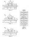
- FIG. 1 ashows the cross-sectional view of a prior art diode 10 structure fabricated on bulk silicon substrate 12 .
- FIG. 1 bshows the cross-sectional view of a prior art diode structure 14 fabricated on a silicon-on-insulator (SOI) wafer that includes substrate 16 and buried oxide 18 .
- SOIsilicon-on-insulator
- This deviceis commonly known as the lateral unidirectional bipolar insulated gate type transistor or lubistor.
- the structures of FIGS. 1 a and 1 bare also known as gated diodes, since a gate stack 20 overlies the body region of the diode.
- the n+ region 22 and p+ region 24are formed on opposite sides of the poly-silicon (poly-Si) gate stack 20 , which is separated from the substrate by a dielectric 26 , typically silicon oxide.
- the n+ and p+ regions 22 and 24 in the substrate in FIG. 1 a and in the active layer in FIG. 1 bare used as the two terminals of the diode.
- the poly-Si gate stack 20 in the structures of FIGS. 1 a and 1 bmay be connected to the cathode (e.g., n+ region 22 ), for example.
- the present inventionprovides a semiconductor diode for electrostatic discharge protection that is compatible with the fabrication processes of advanced transistors and has reduced reverse leakage current.
- a semiconductor diodethat has a substrate with a body region formed in part of the substrate.
- a high permittivity gate dielectriclies between the body region and a gate electrode. P-doped and n-doped regions are adjacent opposite sides of the body region.
- the substratemay be bulk semiconductor, bulk silicon, SiGe, or silicon-on-insulator.
- the high permittivity dielectricmay be aluminum oxide, hafnium oxide, hafnium oxynitride, hafnium silicate, zirconium oxide, zirconium oxynitride, zirconium silicate, yttrium oxide, lanthanum oxide, cerium oxide, titanium oxide, tantalum oxide, or combinations thereof.
- the gate electrodemay be poly-crystalline silicon, poly-crystalline silicon-germanium, a metal, a metallic nitride, a metallic silicide, a metallic oxide, or combinations thereof.
- the gate electrodemay have p-doped and n-doped regions.
- a diode for electrostatic discharge protectionthat has a body region formed in the silicon layer of a silicon-on-insulator substrate.
- a gate electrodeis separated from the body region by a high permittivity gate dielectric. Regions located oppositely adjacent to the body region are doped, respectively, with p-type and n-type dopants.
- Steps of the methodinclude providing a silicon-on-insulator substrate and creating an active region in the silicon layer of the substrate.
- a high permittivity gate dielectricis formed on the active region and a gate electrode is deposited on the gate dielectric. P-doped and n-doped regions are created in the active regions.
- the p-doped and n-doped regionsmay be created by the steps of forming an implant mask and doping a first portion of the active region, then forming another implant mask and doping a second portion of the active region.
- Other aspects of the inventionmay be found in the inclusion of the further step of forming isolation regions surrounding the active region.
- FIGS. 1 a and 1 bare cross section views of diodes according to the prior art
- FIGS. 2 a and 2 bare schematic views of applications of diode devices for electrostatic discharge protection
- FIG. 3is a cross section view of a gated diode indicating leakage current paths
- FIG. 4is a cross section view of an embodiment of the present invention.
- FIG. 5is an energy band diagram
- FIG. 6is a cross section view of another embodiment of the invention.
- FIG. 7is a cross section view of an alternate embodiment of the present invention.
- FIG. 8is a cross section view of a device embodying the invention.
- FIG. 9is a flowchart of steps in the process of fabricating a device according to the present invention.
- FIGS. 10 a through 10 fare cross section views of the results of steps in the process of fabricating a device according to the present invention.
- the present inventionwill be described with respect to preferred embodiments in a specific context, namely a gated diode for use in protecting semiconductor devices from electrostatic discharge damage.
- the inventionmay also be applied, however, to other semiconductor components for which reduced leakage current is a desirable design goal.
- FIGS. 2 a and 2 billustrate how these diodes can be used in for electrostatic discharge (ESD) protection.
- FIG. 3shows examples of leakage paths.
- FIGS. 4-8show various embodiment diodes and FIGS. 9 and 10 a - 10 f are used to discuss one embodiment fabrication process.
- FIGS. 2 a and 2 bshow examples of how the diodes are deployed for protection of integrated circuits.
- a first diode 32is coupled between a supply voltage source V DD and an I/O pad 38 .
- diode 32can include a p-doped region coupled to I/O pad 38 and an n-doped region coupled to V DD .
- a second diode 32 ′is coupled between the I/O pad 38 and a reference voltage V SS or ground. In this case, the p-doped region is coupled to ground and the n-doped region is coupled to the pad.
- the I/O pad 38is provided to indicate any node that might be subject to a high voltage. The most typical of these nodes are the inputs and outputs between the chip and the outside world (e.g., external circuitry when connected to a system or handling devices when the system is being assembled).
- the pad 38is indicated as being an I/O pad, which stands for input/output. It is noted, however, that in this patent the term I/O is meant to include pads for input only, output only or both input and output (or any other node that might be subject to a high voltage).
- FIG. 2 bshows an alternate embodiment where a diode string 28 is used in place of the single diodes 32 and 32 ′ of FIG. 2 b .
- each of the diodes 32 in the diode string 28comprises a diode of the present invention, as will be discussed below.
- only one or more (but not all) of the diodes 32are diodes of the present invention and the remainder are not.
- Semiconductor diodes 32 used for ESD protectionshould have low series resistance, low sub-threshold leakage, and low reverse leakage.
- the series resistanceis an important factor for achieving good ESD performance. ESD protection levels improve with a reduction in diode series resistance.
- the series resistance characteristicis especially important in a mixed voltage environment where diode strings 28 are used and where the series resistance of each diode adds degrading ESD performance.
- Diode resistanceis largely determined by the size of the diode, the resistivity of the material constituting the diode body, the distance of the current path, and the resistance of silicide films or other contacts to n+ and p+ diffusions.
- reverse leakageis another important factor.
- Reverse diode leakage current 30is indicated in FIG. 2 a . A high reverse leakage results in high standby power consumption. In certain advanced IC chip applications, low power consumption is especially important.
- FIG. 3shows a cross-sectional view of a gated diode 100 .
- the diode 100is formed in a bulk semiconductor substrate 102 .
- the substrate 102preferably is a silicon substrate but could include other semiconductors such as germanium, gallium arsenide, or silicon germanium, as examples.
- Shallow trench isolation (STI) regions 104are provided to electrically isolate the diode 100 from other devices (e.g., other diodes and transistors) on the chip. Other types of isolation, such as field isolation, could alternatively be used.
- STIshallow trench isolation
- the gated diode 100includes an n+ doped region 106 and a p+ doped region 108 that are separated by a body region 110 .
- a gate 112overlies the body region 110 and is separated therefrom by a dielectric 114 .
- the gateincludes an n-doped portion 120 adjacent a p-doped portion 122 .
- other conductorscan be used to form the gate 112 .
- the first leakage path 116is a reverse p-n junction leakage current which scales with the area of the p-n junction. A smaller p-n junction area results in a lower leakage.
- the second leakage path 118is a leakage that flows through the gate dielectric or insulator 114 . The first and the second leakage paths both contribute to the reverse diode leakage current 30 indicated in FIG. 2 a . As the gate dielectric becomes thinner with progressive device scaling, the second leakage component will become larger.
- the preferred embodiment of this inventionteaches a device structure that suppresses the second leakage component, and a method for forming the device.
- the current flowing on the second leakage current pathcan be significantly reduced by using gate dielectric that comprises a high permittivity (high-k) material or dielectric with a relative permittivity ⁇ r .
- gate dielectricthat comprises a high permittivity (high-k) material or dielectric with a relative permittivity ⁇ r .
- dielectric layer 114comprises a high-k dielectric.
- the high-k dielectric 114preferably has a permittivity higher than about 5, and more preferably has a permittivity higher than about 10, and even more preferably has a permittivity higher than about 20.
- the high permittivity dielectric 114may be aluminum oxide (Al 2 O 3 ), hafnium oxide (HfO 2 ), hafnium oxynitride (HfON), hafnium silicate (HfSiO 4 ), zirconium oxide (ZrO 2 ), zirconium oxynitride (ZrON), zirconium silicate (ZrSiO 4 ), yttrium oxide (Y 2 O 3 ), lanthanum oxide (La 2 O 3 ), cerium oxide (CeO 2 ), titanium oxide (TiO 2 ), tantalum oxide (Ta 2 O 5 ), or a combination of two or more of these materials.
- the high-k dielectric 114is hafnium oxide.
- the gate dielectric 114may additionally comprise another dielectric material such as silicon oxide, silicon oxynitride, or silicon nitride in addition to the high-k dielectric.
- the gate dielectric 114may be a stack dielectric comprising the high-k dielectric.
- the silicon oxide equivalent thickness (EOT) of the gate dielectricis preferably greater than about 5 angstroms, more preferably greater than about 10 angstroms, and even more preferably greater than about 20 angstroms.
- the physical thickness of the dielectric 114may be greater than about 5 angstroms, more preferably greater than about 20 angstroms, and even more preferably greater than about 40 angstroms. In other embodiments, the physical thickness of the dielectric 114 may be smaller than about 100 angstroms, more preferably smaller than about 50 angstroms, and even more preferably smaller than about 10 angstroms.
- the second leakage path 122passes through an overlap region 124 between the gate electrode 112 and one of the doped regions 108 .
- the anode or p-doped region 108is electrically connected to a grounded I/O pad (see e.g., FIG. 2 a ) and where the cathode or n-doped region 106 is electrically connected to the supply voltage (again see e.g., FIG. 2 a )
- the energy band diagram along the line A-A′ in FIG. 4is depicted in FIG. 5 .
- the energy band diagram of FIG. 5shows the grounded p-doped region 108 and the p-doped gate electrode region 122 biased at the supply voltage.
- a depletion region 126exists in the p-doped region 108 and an accumulation region 128 exists in the p-doped portion 122 of gate electrode 112 .
- the accumulation regionis comprised of holes. Quantum mechanical tunneling of the holes from the gate electrode 122 through the dielectric 114 to the p-doped region 108 results in a leakage current.
- the gate dielectriccan be made thicker for the same capacitance, and the thicker gate dielectric effectively suppresses the tunneling leakage current.
- a conductive material 130may be formed to strap the n-doped and p-doped regions 120 and 122 in the gate electrode 112 , as well as at 134 to strap the n-doped region 106 and at 132 to strap the p-doped region 108 of the substrate.
- the conductive material 130(and 132 and 134 ) can be a metal, a metallic nitride, a metallic silicide, or a metallic oxide, or combinations thereof. Metals such as molybdenum, tungsten, titanium, tantalum, platinum, and hafnium may be used.
- Metallic nitridesmay be used, including but not restricted to, molybdenum nitride, tungsten nitride, titanium nitride, and tantalum nitride.
- Metallic silicidesmay be used, including but not restricted to, nickel silicide, cobalt silicide, tungsten silicide, titanium silicide, tantalum silicide, platinum silicide, and erbium silicide.
- Metallic oxidesmay also be used, including but not restricted to, ruthenium oxide, and indium tin oxide.
- the isolation region 104 in FIG. 4comprises a dielectric filling material, preferably silicon oxide. However, it is understood that any other dielectric material or combinations of dielectric materials may be used to form the isolation region.
- the spacers 136are formed on the sides of the gate electrode 112 and may comprise a dielectric material such as silicon nitride or silicon oxide.
- the spacersmay be simple spacers as shown in FIG. 4 , or the spacers may be composite spacers known and used in the art.
- FIG. 6shows another embodiment of the present invention where the gated diode 100 is formed on a semiconductor-on-insulator substrate.
- Trench isolationin this case shallow trench isolation 104 , is used in this example.
- the semiconductor-on-insulator substratepreferably has a silicon layer (that includes p-doped region 108 , body region 110 , and n-doped region 106 ) overlying a silicon oxide insulator layer 142 , on top of a substrate 140 .
- the thickness (t Si ) of silicon layer 106 / 108 / 110is preferably in the range of about 20 angstroms to about 1000 angstroms, and more preferably in the range of about 20 angstroms to about 300 angstroms.
- the use of a thin silicon layerresults in a small junction area and therefore a low reverse leakage.
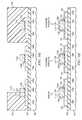
- FIG. 7shows yet another embodiment of the invention where the gated diode 100 is formed on a semiconductor-on-insulator substrate and mesa isolation is used.
- mesa isolationBy using mesa isolation, the surfaces 144 of the insulator layer 142 not covered by the semiconductor layer are exposed during the formation of the device, and the exposed insulator layer 144 may be potentially etched or recessed during chemical processing. Forming a layer of nitride to protect surfaces 144 may prevent this etching of insulator layer 142 .
- Conductive materialsuch as a metal silicide (not shown) may be formed on the gate electrode 112 and the doped regions 106 and 108 .
- FIG. 8shows an alternative embodiment of the invention where the gate electrode 112 comprises a metal, such as metal silicide, metal nitride, or combinations thereof. While illustrated for the example of an SOI device with mesa isolation, it is understood that any of the embodiments described herein can include a metal gate.
- the gate electrode 112 in this embodimentdoes not contain poly-silicon or poly-silicon-germanium. Examples of metals include molybdenum, tungsten, titanium, tantalum, platinum, and hafnium may be used.
- Metallic nitridesmay be used, including but not restricted to, molybdenum nitride, tungsten nitride, titanium nitride, and tantalum nitride.
- Metallic silicidesmay be used, including but not restricted to, nickel silicide, cobalt silicide, tungsten silicide, titanium silicide, tantalum silicide, platinum silicide, and erbium silicide.
- Metallic oxidesmay also be used, including but not restricted to, ruthenium oxide, and indium tin oxide.
- FIG. 9is a flowchart of process steps for forming a diode structure according to the present invention.
- FIGS. 10 a - 10 fshow cross-sectional views of formation of the diode as well as an n-channel and a p-channel CMOS transistor.
- an SOI substrateincludes a substrate 140 with an overlying insulating layer 142 and a semiconductor layer 144 .
- a semiconductor-on-insulator substrate or a bulk semiconductor substratemay also be used.
- Active regionsare formed in a silicon layer of the silicon-on-insulator substrate.
- Three active regions 146 a , 146 b and 146 care shown in FIG. 10 b .
- a diode (or lubistor)will be formed in active region 146 a
- an n-channel transistorwill be formed in active region 146 b
- a p-channel transistorwill be formed in active region 146 c .
- Other active areas(not shown) will include one or more of these or other devices.
- Active regions 146are isolated in this embodiment by isolation regions, a technique known as mesa isolation. With mesa isolation, an air gap is formed between the mesa regions 146 to isolate these regions during device fabrication. Before metallization, these trench regions will be filled with a dielectric such as silicon oxide, doped glass or such. In another embodiment, shallow trench isolation is used. In this embodiment, the trenches between active areas are filled with an insulator, such as silicon oxide.
- a dielectric 114is next deposited over active regions 146 .
- dielectric 114also covers the buried insulator 142 between the active areas 146 . This result is optional.
- dielectric 114is preferably a high permittivity material.
- the gate dielectric 114can be formed by a chemical vapor deposition step or a sputtering deposition step. In the preferred embodiment, the gate dielectric 114 is formed by first forming an interfacial oxide layer and then forming a high permittivity dielectric layer.
- Gate electrode material 112is next deposited on dielectric 114 and etched to form gate electrodes 112 a , 112 b and 112 c , as shown in FIG. 10 c .
- the gate electrode materialis preferably poly-crystalline silicon, but silicon-germanium, a metal, a metal silicide, a metal nitride, a metal oxide, or combinations thereof may also be used.
- the gate dielectric 114 not covered by the gate electrode 112may be removed, as shown, or may be left covering the active region 146 .
- implant mask 148is used to mask the active region 146 b and a portion of the active region 146 a adjacent a first edge of the gate electrode 112 a .
- Dopants of a first typeare introduced to dope regions 108 of the unmasked active regions 146 , and implant mask 148 is removed.
- dopants of the first typeare p-type dopants.
- the dopantsmay also dope regions 122 a of gate electrodes 112 .
- the doping stepsimultaneously forms the source and drain regions 108 c of the p-channel transistor in active area 146 c and the p-doped region 108 a of the diode in active region 146 a (as well as other p-doped regions on the chip).
- implant mask 150is formed so that dopants of a second type can be introduced into regions 106 of the active regions 146 a and 146 b and region 120 of the gate electrode 112 a .
- the dopants of the second typeare n-type dopants.
- Implant mask 150is removed after the introduction of dopants of the second type.
- the doping stepsimultaneously forms the source and drain regions 106 b of the n-channel transistor in active area 146 b and the n-doped region 106 a of the diode in active region 146 a (as well as other n-doped regions on the chip).
- Regions 106 and 108are typically doped to a concentration in the range of about 10 16 cm ⁇ 3 to about 10 20 cm ⁇ 3 , but preferably to a concentration greater than about 10 19 cm ⁇ 3 .
- Implant masks 148 and 150are preferably photoresist, but may also be silicon oxide, silicon nitride, or other masking materials.
- Spacers 136may be formed on the sides of the gate electrodes 112 as shown in FIG. 10 f . Additional dopants may be introduced into the active regions 146 and/or the gate electrode 112 after the formation of the spacers. These steps are included to maintain compatibility with CMOS processing used to form the n-channel and p-channel transistors on the chip. For example, the sidewall spacers 136 are formed on the transistor sidewalls and the additional dopants can be introduced during the source/drain implants of the transistors. While not shown (see e.g., FIGS. 10 d and 10 ), masking steps are preferably used in forming the more heavily doped regions.
- a conductive material 130such as a metal silicide, may be formed on the gate electrodes 112 and on the doped regions 106 and 108 to improve their conductivity.
- a conductive material(see elements 130 , 132 and 134 in FIG. 4 for example) can be simultaneously formed on the source, drain and gates of transistors and the doped regions and gate of the diodes that are on the same chip.
Landscapes
- Semiconductor Integrated Circuits (AREA)
- Metal-Oxide And Bipolar Metal-Oxide Semiconductor Integrated Circuits (AREA)
- Insulated Gate Type Field-Effect Transistor (AREA)
Abstract
Description
- The present invention relates to the field of semiconductor devices, and more specifically, to a semiconductor diode device for electrostatic discharge protection in advanced complementary metal-oxide-semiconductor (CMOS) technologies.
- Transistor size reduction has resulted in the thinning of insulator layers such as the gate dielectric. These thinner dielectric layers fail at lower voltages. Consequently, device scaling increases circuit sensitivity to voltage stress, electrical overstress (EOS), and electrostatic discharge (ESD). These types of failures are a major concern in advanced semiconductor technology. This is especially true for integrated circuit (IC) chips that interface with other chips or signals with voltages above that of the IC chip itself.
- Silicon based ICs are particularly susceptible to electrostatic discharge damage, for example in the situation where a user of a device containing an integrated circuit develops a static charge on their body and subsequently comes in contact with the device containing the integrated circuit. The electrostatic discharge induced in a human body may produce a voltage in excess of 5000 volts. Such a high instantaneous voltage may catastrophically damage the integrated circuit.
- Therefore, IC chips usually include protection devices or diodes in interface circuits to provide the IC chip with added ESD protection. U.S. Pat. No. 5,629,544, entitled “Semiconductor diode with silicide films and trench isolation,” issued to Voldman et al. teaches the use of diode structures bound by poly-silicon for the protection of bulk silicon and silicon-on-insulator (SOI) circuits. U.S. Pat. No. 6,015,993 and U.S. Pat. No. 6,232,163, both issued to Voldman et al., discuss a high voltage tolerant diode structure for mixed-voltage and mixed signal and analog/digital applications. These prior arts are applicable to bulk and SOI transistor technologies.
FIG. 1 ashows the cross-sectional view of aprior art diode 10 structure fabricated onbulk silicon substrate 12.FIG. 1 bshows the cross-sectional view of a priorart diode structure 14 fabricated on a silicon-on-insulator (SOI) wafer that includessubstrate 16 and buriedoxide 18. This device is commonly known as the lateral unidirectional bipolar insulated gate type transistor or lubistor. The structures ofFIGS. 1 aand1bare also known as gated diodes, since agate stack 20 overlies the body region of the diode.- In both these structures, the
n+ region 22 andp+ region 24 are formed on opposite sides of the poly-silicon (poly-Si)gate stack 20, which is separated from the substrate by a dielectric26, typically silicon oxide. The n+ andp+ regions FIG. 1 aand in the active layer inFIG. 1 bare used as the two terminals of the diode. The poly-Si gate stack20 in the structures ofFIGS. 1 aand1bmay be connected to the cathode (e.g., n+ region22), for example. - The present invention provides a semiconductor diode for electrostatic discharge protection that is compatible with the fabrication processes of advanced transistors and has reduced reverse leakage current.
- Aspects of the invention can be found in a semiconductor diode that has a substrate with a body region formed in part of the substrate. A high permittivity gate dielectric lies between the body region and a gate electrode. P-doped and n-doped regions are adjacent opposite sides of the body region. The substrate may be bulk semiconductor, bulk silicon, SiGe, or silicon-on-insulator. The high permittivity dielectric may be aluminum oxide, hafnium oxide, hafnium oxynitride, hafnium silicate, zirconium oxide, zirconium oxynitride, zirconium silicate, yttrium oxide, lanthanum oxide, cerium oxide, titanium oxide, tantalum oxide, or combinations thereof. The gate electrode may be poly-crystalline silicon, poly-crystalline silicon-germanium, a metal, a metallic nitride, a metallic silicide, a metallic oxide, or combinations thereof. The gate electrode may have p-doped and n-doped regions.
- Further aspects of the invention may be found in a diode for electrostatic discharge protection that has a body region formed in the silicon layer of a silicon-on-insulator substrate. A gate electrode is separated from the body region by a high permittivity gate dielectric. Regions located oppositely adjacent to the body region are doped, respectively, with p-type and n-type dopants.
- Still further aspects of the invention can be found in a method of making a diode. Steps of the method include providing a silicon-on-insulator substrate and creating an active region in the silicon layer of the substrate. A high permittivity gate dielectric is formed on the active region and a gate electrode is deposited on the gate dielectric. P-doped and n-doped regions are created in the active regions.
- Aspects of the invention may be found where the p-doped and n-doped regions may be created by the steps of forming an implant mask and doping a first portion of the active region, then forming another implant mask and doping a second portion of the active region. Other aspects of the invention may be found in the inclusion of the further step of forming isolation regions surrounding the active region.
- The foregoing has outlined rather broadly the features and technical advantages of the present invention in order that the detailed description of the invention that follows may be better understood. Additional features and advantages of the invention will be described hereinafter which form the subject of the claims of the invention. It should be appreciated by those skilled in the art that the conception and specific embodiment disclosed may be readily utilized as a basis for modifying or designing other structures or processes for carrying out the same purposes of the present invention. It should also be realized by those skilled in the art that such equivalent constructions do not depart from the spirit and scope of the invention as set forth in the appended claims.
- For a more complete understanding of the present invention, and the advantages thereof, reference is now made to the following descriptions taken in conjunction with the accompanying drawing, in which:
FIGS. 1 aand1bare cross section views of diodes according to the prior art;FIGS. 2 aand2bare schematic views of applications of diode devices for electrostatic discharge protection;FIG. 3 is a cross section view of a gated diode indicating leakage current paths;FIG. 4 is a cross section view of an embodiment of the present invention;FIG. 5 is an energy band diagram;FIG. 6 is a cross section view of another embodiment of the invention;FIG. 7 is a cross section view of an alternate embodiment of the present invention;FIG. 8 is a cross section view of a device embodying the invention;FIG. 9 is a flowchart of steps in the process of fabricating a device according to the present invention; andFIGS. 10 athrough10fare cross section views of the results of steps in the process of fabricating a device according to the present invention.- The making and using of the presently preferred embodiments are discussed in detail below. It should be appreciated, however, that the present invention provides many applicable inventive concepts that can be embodied in a wide variety of specific contexts. The specific embodiments discussed are merely illustrative of specific ways to make and use the invention, and do not limit the scope of the invention.
- The present invention will be described with respect to preferred embodiments in a specific context, namely a gated diode for use in protecting semiconductor devices from electrostatic discharge damage. The invention may also be applied, however, to other semiconductor components for which reduced leakage current is a desirable design goal.
- As will be discussed in greater detail below, the preferred embodiment of the present invention relates to a diode that has reduced leakage.
FIGS. 2 aand2billustrate how these diodes can be used in for electrostatic discharge (ESD) protection.FIG. 3 shows examples of leakage paths.FIGS. 4-8 show various embodiment diodes andFIGS. 9 and 10 a-10fare used to discuss one embodiment fabrication process. FIGS. 2 aand2bshow examples of how the diodes are deployed for protection of integrated circuits. Referring first toFIG. 2 a, afirst diode 32 is coupled between a supply voltage source VDDand an I/O pad 38. For example,diode 32 can include a p-doped region coupled to I/O pad 38 and an n-doped region coupled to VDD. Asecond diode 32′ is coupled between the I/O pad 38 and a reference voltage VSSor ground. In this case, the p-doped region is coupled to ground and the n-doped region is coupled to the pad.- The I/
O pad 38 is provided to indicate any node that might be subject to a high voltage. The most typical of these nodes are the inputs and outputs between the chip and the outside world (e.g., external circuitry when connected to a system or handling devices when the system is being assembled). Thepad 38 is indicated as being an I/O pad, which stands for input/output. It is noted, however, that in this patent the term I/O is meant to include pads for input only, output only or both input and output (or any other node that might be subject to a high voltage). FIG. 2 bshows an alternate embodiment where adiode string 28 is used in place of thesingle diodes FIG. 2 b. In the preferred embodiment, each of thediodes 32 in thediode string 28 comprises a diode of the present invention, as will be discussed below. In an alternate embodiment, only one or more (but not all) of thediodes 32 are diodes of the present invention and the remainder are not.Semiconductor diodes 32 used for ESD protection should have low series resistance, low sub-threshold leakage, and low reverse leakage. The series resistance is an important factor for achieving good ESD performance. ESD protection levels improve with a reduction in diode series resistance. The series resistance characteristic is especially important in a mixed voltage environment where diode strings28 are used and where the series resistance of each diode adds degrading ESD performance.- Diode resistance is largely determined by the size of the diode, the resistivity of the material constituting the diode body, the distance of the current path, and the resistance of silicide films or other contacts to n+ and p+ diffusions. In addition, reverse leakage is another important factor. Reverse diode leakage current30 is indicated in
FIG. 2 a. A high reverse leakage results in high standby power consumption. In certain advanced IC chip applications, low power consumption is especially important. FIG. 3 shows a cross-sectional view of agated diode 100. In this example, thediode 100 is formed in abulk semiconductor substrate 102. Thesubstrate 102 preferably is a silicon substrate but could include other semiconductors such as germanium, gallium arsenide, or silicon germanium, as examples. Shallow trench isolation (STI)regions 104 are provided to electrically isolate thediode 100 from other devices (e.g., other diodes and transistors) on the chip. Other types of isolation, such as field isolation, could alternatively be used.- The
gated diode 100 includes an n+ dopedregion 106 and a p+ dopedregion 108 that are separated by abody region 110. Agate 112 overlies thebody region 110 and is separated therefrom by a dielectric114. In the illustrated embodiment, the gate includes an n-dopedportion 120 adjacent a p-dopedportion 122. In other embodiments, other conductors can be used to form thegate 112. - Two of the reverse leakage paths in a semiconductor gated
diode 100 are illustrated inFIG. 3 . Thefirst leakage path 116 is a reverse p-n junction leakage current which scales with the area of the p-n junction. A smaller p-n junction area results in a lower leakage. Thesecond leakage path 118 is a leakage that flows through the gate dielectric orinsulator 114. The first and the second leakage paths both contribute to the reverse diode leakage current30 indicated inFIG. 2 a. As the gate dielectric becomes thinner with progressive device scaling, the second leakage component will become larger. The preferred embodiment of this invention teaches a device structure that suppresses the second leakage component, and a method for forming the device. - With the techniques of the preferred embodiment, the current flowing on the second leakage current path can be significantly reduced by using gate dielectric that comprises a high permittivity (high-k) material or dielectric with a relative permittivity εr. A detailed cross-sectional view of a diode structure embodying the invention is shown in
FIG. 4 . - Referring now to
FIG. 4 ,dielectric layer 114 comprises a high-k dielectric. The high-k dielectric 114 preferably has a permittivity higher than about 5, and more preferably has a permittivity higher than about 10, and even more preferably has a permittivity higher than about 20. Thehigh permittivity dielectric 114 may be aluminum oxide (Al2O3), hafnium oxide (HfO2), hafnium oxynitride (HfON), hafnium silicate (HfSiO4), zirconium oxide (ZrO2), zirconium oxynitride (ZrON), zirconium silicate (ZrSiO4), yttrium oxide (Y2O3), lanthanum oxide (La2O3), cerium oxide (CeO2), titanium oxide (TiO2), tantalum oxide (Ta2O5), or a combination of two or more of these materials. - In the preferred embodiment, the high-
k dielectric 114 is hafnium oxide. Thegate dielectric 114 may additionally comprise another dielectric material such as silicon oxide, silicon oxynitride, or silicon nitride in addition to the high-k dielectric. In other words, thegate dielectric 114 may be a stack dielectric comprising the high-k dielectric. - The silicon oxide equivalent thickness (EOT) of the gate dielectric is preferably greater than about 5 angstroms, more preferably greater than about 10 angstroms, and even more preferably greater than about 20 angstroms. The physical thickness of the dielectric114 may be greater than about 5 angstroms, more preferably greater than about 20 angstroms, and even more preferably greater than about 40 angstroms. In other embodiments, the physical thickness of the dielectric114 may be smaller than about 100 angstroms, more preferably smaller than about 50 angstroms, and even more preferably smaller than about 10 angstroms.
- The
second leakage path 122 passes through anoverlap region 124 between thegate electrode 112 and one of the dopedregions 108. In the example where the anode or p-dopedregion 108 is electrically connected to a grounded I/O pad (see e.g.,FIG. 2 a) and where the cathode or n-dopedregion 106 is electrically connected to the supply voltage (again see e.g.,FIG. 2 a), the energy band diagram along the line A-A′ inFIG. 4 is depicted inFIG. 5 . - The energy band diagram of
FIG. 5 shows the grounded p-dopedregion 108 and the p-dopedgate electrode region 122 biased at the supply voltage. As a result of such a bias configuration, adepletion region 126 exists in the p-dopedregion 108 and anaccumulation region 128 exists in the p-dopedportion 122 ofgate electrode 112. The accumulation region is comprised of holes. Quantum mechanical tunneling of the holes from thegate electrode 122 through the dielectric114 to the p-dopedregion 108 results in a leakage current. By using a high-k material forgate dielectric 114, the gate dielectric can be made thicker for the same capacitance, and the thicker gate dielectric effectively suppresses the tunneling leakage current. - Returning to
FIG. 4 , aconductive material 130 may be formed to strap the n-doped and p-dopedregions gate electrode 112, as well as at134 to strap the n-dopedregion 106 and at132 to strap the p-dopedregion 108 of the substrate. The conductive material130 (and132 and134) can be a metal, a metallic nitride, a metallic silicide, or a metallic oxide, or combinations thereof. Metals such as molybdenum, tungsten, titanium, tantalum, platinum, and hafnium may be used. Metallic nitrides may be used, including but not restricted to, molybdenum nitride, tungsten nitride, titanium nitride, and tantalum nitride. Metallic silicides may be used, including but not restricted to, nickel silicide, cobalt silicide, tungsten silicide, titanium silicide, tantalum silicide, platinum silicide, and erbium silicide. Metallic oxides may also be used, including but not restricted to, ruthenium oxide, and indium tin oxide. - The
isolation region 104 inFIG. 4 comprises a dielectric filling material, preferably silicon oxide. However, it is understood that any other dielectric material or combinations of dielectric materials may be used to form the isolation region. - The
spacers 136 are formed on the sides of thegate electrode 112 and may comprise a dielectric material such as silicon nitride or silicon oxide. The spacers may be simple spacers as shown inFIG. 4 , or the spacers may be composite spacers known and used in the art. FIG. 6 shows another embodiment of the present invention where thegated diode 100 is formed on a semiconductor-on-insulator substrate. Trench isolation, in this caseshallow trench isolation 104, is used in this example. InFIG. 6 , the semiconductor-on-insulator substrate preferably has a silicon layer (that includes p-dopedregion 108,body region 110, and n-doped region106) overlying a siliconoxide insulator layer 142, on top of asubstrate 140. The thickness (tSi) ofsilicon layer 106/108/110 is preferably in the range of about 20 angstroms to about 1000 angstroms, and more preferably in the range of about 20 angstroms to about 300 angstroms. The use of a thin silicon layer results in a small junction area and therefore a low reverse leakage.FIG. 7 shows yet another embodiment of the invention where thegated diode 100 is formed on a semiconductor-on-insulator substrate and mesa isolation is used. By using mesa isolation, thesurfaces 144 of theinsulator layer 142 not covered by the semiconductor layer are exposed during the formation of the device, and the exposedinsulator layer 144 may be potentially etched or recessed during chemical processing. Forming a layer of nitride to protectsurfaces 144 may prevent this etching ofinsulator layer 142. Conductive material such as a metal silicide (not shown) may be formed on thegate electrode 112 and the dopedregions FIG. 8 shows an alternative embodiment of the invention where thegate electrode 112 comprises a metal, such as metal silicide, metal nitride, or combinations thereof. While illustrated for the example of an SOI device with mesa isolation, it is understood that any of the embodiments described herein can include a metal gate. Thegate electrode 112 in this embodiment does not contain poly-silicon or poly-silicon-germanium. Examples of metals include molybdenum, tungsten, titanium, tantalum, platinum, and hafnium may be used. Metallic nitrides may be used, including but not restricted to, molybdenum nitride, tungsten nitride, titanium nitride, and tantalum nitride. Metallic silicides may be used, including but not restricted to, nickel silicide, cobalt silicide, tungsten silicide, titanium silicide, tantalum silicide, platinum silicide, and erbium silicide. Metallic oxides may also be used, including but not restricted to, ruthenium oxide, and indium tin oxide.- Next, a method of forming the diode structure is described.
FIG. 9 is a flowchart of process steps for forming a diode structure according to the present invention.FIGS. 10 a-10fshow cross-sectional views of formation of the diode as well as an n-channel and a p-channel CMOS transistor. - Referring first to
FIG. 10 a, an SOI substrate includes asubstrate 140 with an overlying insulatinglayer 142 and asemiconductor layer 144. However, it will be understood that a semiconductor-on-insulator substrate or a bulk semiconductor substrate may also be used. Active regions are formed in a silicon layer of the silicon-on-insulator substrate. Threeactive regions FIG. 10 b. In this example, a diode (or lubistor) will be formed inactive region 146a, an n-channel transistor will be formed inactive region 146b, and a p-channel transistor will be formed inactive region 146c. Other active areas (not shown) will include one or more of these or other devices. - Active regions146 are isolated in this embodiment by isolation regions, a technique known as mesa isolation. With mesa isolation, an air gap is formed between the mesa regions146 to isolate these regions during device fabrication. Before metallization, these trench regions will be filled with a dielectric such as silicon oxide, doped glass or such. In another embodiment, shallow trench isolation is used. In this embodiment, the trenches between active areas are filled with an insulator, such as silicon oxide.
- A dielectric114 is next deposited over active regions146. In the illustrated embodiment, dielectric114 also covers the buried
insulator 142 between the active areas146. This result is optional. As described previously, dielectric114 is preferably a high permittivity material. Thegate dielectric 114 can be formed by a chemical vapor deposition step or a sputtering deposition step. In the preferred embodiment, thegate dielectric 114 is formed by first forming an interfacial oxide layer and then forming a high permittivity dielectric layer. Gate electrode material 112 is next deposited ondielectric 114 and etched to formgate electrodes FIG. 10 c. The gate electrode material is preferably poly-crystalline silicon, but silicon-germanium, a metal, a metal silicide, a metal nitride, a metal oxide, or combinations thereof may also be used. Thegate dielectric 114 not covered by thegate electrode 112 may be removed, as shown, or may be left covering the active region146.- Turning now to
FIG. 10 d,implant mask 148 is used to mask theactive region 146band a portion of theactive region 146aadjacent a first edge of thegate electrode 112a. Dopants of a first type are introduced todope regions 108 of the unmasked active regions146, andimplant mask 148 is removed. In this embodiment of the invention, dopants of the first type are p-type dopants. The dopants may alsodope regions 122aofgate electrodes 112. As shown, the doping step simultaneously forms the source and drainregions 108cof the p-channel transistor inactive area 146cand the p-dopedregion 108aof the diode inactive region 146a(as well as other p-doped regions on the chip). - Next, as shown in
FIG. 10 e,implant mask 150 is formed so that dopants of a second type can be introduced intoregions 106 of theactive regions region 120 of thegate electrode 112a. In this embodiment of the invention, the dopants of the second type are n-type dopants.Implant mask 150 is removed after the introduction of dopants of the second type. As shown, the doping step simultaneously forms the source and drainregions 106bof the n-channel transistor inactive area 146band the n-dopedregion 106aof the diode inactive region 146a(as well as other n-doped regions on the chip). - Both types of dopants may be introduced by conventional ion implantation, by plasma immersion ion implantation, or other known techniques of introducing dopants.
Regions Spacers 136 may be formed on the sides of thegate electrodes 112 as shown inFIG. 10 f. Additional dopants may be introduced into the active regions146 and/or thegate electrode 112 after the formation of the spacers. These steps are included to maintain compatibility with CMOS processing used to form the n-channel and p-channel transistors on the chip. For example, thesidewall spacers 136 are formed on the transistor sidewalls and the additional dopants can be introduced during the source/drain implants of the transistors. While not shown (see e.g.,FIGS. 10 dand10), masking steps are preferably used in forming the more heavily doped regions.- As shown in
FIG. 10 f, aconductive material 130, such as a metal silicide, may be formed on thegate electrodes 112 and on the dopedregions elements FIG. 4 for example) can be simultaneously formed on the source, drain and gates of transistors and the doped regions and gate of the diodes that are on the same chip. - Although the present invention and its advantages have been described in detail, it should be understood that various changes, substitutions and alterations can be made herein without departing from the spirit and scope of the invention as defined by the appended claims.
Claims (89)
1. A semiconductor diode comprising:
a substrate;
a body region formed in a portion of the substrate;
a gate dielectric overlying the body region, said gate dielectric comprising a high permittivity dielectric;
a gate electrode overlying the gate dielectric; and
a p-doped region and an n-doped region formed in the substrate oppositely adjacent to the body region.
2. The diode ofclaim 1 wherein the substrate is a bulk semiconductor substrate.
3. The diode ofclaim 2 wherein the substrate is a bulk silicon substrate.
4. The diode ofclaim 1 wherein the substrate comprises silicon and germanium.
5. The diode ofclaim 1 wherein the substrate is a silicon-on-insulator substrate comprising a silicon layer overlying an insulator layer wherein the body region, the p-doped region and the n-doped region are formed in the silicon layer.
6. The diode ofclaim 5 wherein the insulator layer is silicon oxide.
7. The diode ofclaim 5 wherein the silicon layer has a thickness in the range of about 20 angstroms to about 1000 angstroms.
8. The diode ofclaim 5 wherein the silicon layer has a thickness in the range of about 20 angstroms to about 300 angstroms.
9. The diode ofclaim 1 wherein the gate electrode comprises poly-crystalline silicon.
10. The diode ofclaim 9 further comprising metal silicide formed on the gate electrode, the p-doped region, and the n-doped region.
11. The diode ofclaim 9 wherein a first portion of the gate electrode is doped p-type and a second portion of the gate electrode is doped n-type.
12. The diode ofclaim 1 wherein the gate electrode is formed from a material selected from the group consisting of a metal, a metallic nitride, a metallic silicide, a metallic oxide, and combinations thereof.
13. The diode ofclaim 1 wherein the gate electrode is formed from a material selected from the group consisting of molybdenum, tungsten, titanium, tantalum, platinum, and hafnium.
14. The diode ofclaim 1 wherein the gate electrode is formed from a material selected from the group consisting of molybdenum nitride, tungsten nitride, titanium nitride, tantalum nitride, and combinations thereof.
15. The diode ofclaim 1 wherein the gate electrode is formed from a material selected from the group consisting of nickel silicide, cobalt silicide, tungsten silicide, titanium silicide, tantalum silicide, platinum silicide, erbium silicide, and combinations thereof.
16. The diode ofclaim 1 wherein the gate electrode is formed from a material selected from the group consisting of ruthenium oxide, indium tin oxide, and combinations thereof.
17. The diode ofclaim 1 wherein the high permittivity dielectric is selected from the group consisting of aluminum oxide, hafnium oxide, hafnium oxynitride, hafnium silicate, zirconium oxide, zirconium oxynitride, zirconium silicate, yttrium oxide, lanthanum oxide, cerium oxide, titanium oxide, tantalum oxide, and combinations thereof.
18. The diode ofclaim 1 wherein the high permittivity dielectric has a relative permittivity larger than about 5.
19. The diode ofclaim 1 wherein the high permittivity dielectric has a relative permittivity larger than about 10.
20. The diode ofclaim 1 wherein the high permittivity dielectric has a relative permittivity larger than about 20.
21. The diode ofclaim 1 wherein the gate dielectric has a physical thickness less than about 100 angstroms.
22. The diode ofclaim 1 wherein the gate dielectric has a physical thickness less than about 50 angstroms.
23. The diode ofclaim 1 wherein the gate dielectric has a physical thickness less than about 10 angstroms.
24. The diode ofclaim 1 wherein at least one doped region has a doping concentration of greater than about 1019cm−3.
25. The diode ofclaim 1 and further comprising spacers on the sides of the gate electrode.
26. The diode ofclaim 25 wherein the material of the spacers is selected from the group consisting of silicon oxide, silicon oxynitride, silicon nitride, and combinations thereof.
27. A semiconductor device including electrostatic discharge protection, the device comprising:
a silicon-on-insulator substrate, comprising a silicon layer overlying an insulator layer;
a first doped region formed in the silicon layer and being doped with dopants of a first conductivity type;
a second doped region formed in the silicon layer and being doped with dopants of a second conductivity type, the second conductivity type being opposite the first conductivity type;
a body region formed in the silicon layer between the first doped region and the second doped region;
a high permittivity gate dielectric overlying the body region;
a gate electrode overlying the gate dielectric;
an input/output pad electrically coupled to the first doped region; and
a reference voltage node coupled to the second doped region.
28. The device ofclaim 27 where the insulator layer comprises silicon oxide.
29. The device ofclaim 27 wherein the silicon layer has a thickness in the range of about 20 angstroms to about 1000 angstroms.
30. The device ofclaim 27 wherein the silicon layer has a thickness in the range of about 20 angstroms to about 300 angstroms.
31. The device ofclaim 27 wherein the gate electrode comprises poly-crystalline silicon.
32. The device ofclaim 31 further comprising metal silicide formed on the gate electrode, the first doped region, and the second doped region.
33. The device ofclaim 31 wherein a first portion of the gate electrode is doped p-type and a second portion of the gate electrode is doped n-type.
34. The device ofclaim 27 wherein the gate electrode is formed from a material selected from the group consisting of a metal, a metallic nitride, a metallic silicide, a metallic oxide, and combinations thereof.
35. The device ofclaim 27 wherein the gate electrode is formed from a material selected from the group consisting of molybdenum, tungsten, titanium, tantalum, platinum, and hafnium.
36. The device ofclaim 27 wherein the gate electrode is formed from a material selected from the group consisting of molybdenum nitride, tungsten nitride, titanium nitride, tantalum nitride, and combinations thereof.
37. The device ofclaim 27 wherein the gate electrode is formed from a material selected from the group consisting of nickel silicide, cobalt silicide, tungsten silicide, titanium silicide, tantalum silicide, platinum silicide, erbium silicide, and combinations thereof.
38. The device ofclaim 27 wherein the gate electrode is formed from a material selected from the group consisting of ruthenium oxide, indium tin oxide, and combinations thereof.
39. The device ofclaim 27 wherein the high permittivity dielectric is selected from the group consisting of aluminum oxide, hafnium oxide, hafnium oxynitride, hafnium silicate, zirconium oxide, zirconium oxynitride, zirconium silicate, yttrium oxide, lanthanum oxide, cerium oxide, titanium oxide, tantalum oxide, and combinations thereof.
40. The device ofclaim 27 wherein the high permittivity dielectric has a relative permittivity larger than about 5.
41. The device ofclaim 27 wherein the high permittivity dielectric has a relative permittivity larger than about 10.
42. The device ofclaim 27 wherein the high permittivity dielectric has a relative permittivity larger than about 20.
43. The device ofclaim 27 wherein the gate dielectric has a physical thickness less than about 100 angstroms.
44. The device ofclaim 27 wherein the gate dielectric has a physical thickness less than about 50 angstroms.
45. The device ofclaim 27 wherein the gate dielectric has a physical thickness less than about 10 angstroms.
46. The device ofclaim 27 wherein at least one doped region has a doping concentration of greater than 1019cm−3.
47. The device ofclaim 27 further comprising spacers on the sides of the gate electrode.
48. The device ofclaim 47 wherein the spacers comprise a material selected from the group consisting of silicon oxide, silicon oxynitride, silicon nitride, and combinations thereof.
49. The device ofclaim 27 wherein the first doped region comprises a p-type region that is electrically coupled to the input/output pad and the second doped region comprises an n-type region that is electrically coupled to a VDDpower supply.
50. The device ofclaim 27 wherein the second doped region comprises a p-type region that is electrically coupled to a ground line and the second doped region comprises an n-type region that is electrically coupled to the input/output pad.
51. A method of forming a diode, the method comprising:
providing a silicon-on-insulator substrate including a silicon layer overlying an insulator layer;
creating an active region in the silicon layer;
forming a gate dielectric on the active region, the gate dielectric comprising a high permittivity dielectric;
forming a gate electrode on the gate dielectric;
forming a p-doped region in the active region adjacent a first edge of the gate electrode; and
forming an n-doped region in the active region adjacent a second edge of the gate electrode, the first edge being opposed to the second edge.
52. The method ofclaim 51 wherein the steps of forming a p-doped region and forming an n-doped region comprise:
forming a first implant mask exposing a first portion of the active region;
doping the first portion of the silicon layer;
forming a second implant mask exposing a second portion of the active region; and
doping the second portion of the silicon layer.
53. The method ofclaim 51 further comprising:
forming isolation regions surrounding the active region; and
doping the active region.
54. The method ofclaim 51 wherein the p-doped region and the n-doped region are doped to a dopant concentration greater than about 1019cm−3.
55. The method ofclaim 51 wherein forming the gate dielectric comprises a chemical vapor deposition step or a sputtering deposition step.
56. The method ofclaim 51 wherein forming the gate dielectric comprises:
forming an interfacial oxide layer; and
forming a high permittivity dielectric layer.
57. The method ofclaim 51 further comprising the step of creating spacers on sides of the gate electrode.
58. The method ofclaim 57 wherein the material of the spacers is selected from the group composed of silicon oxide, silicon oxynitride, silicon nitride, and combinations thereof.
59. The method ofclaim 51 wherein the silicon layer has a thickness in the range of about 20 angstroms to about 1000 angstroms.
60. The method ofclaim 51 wherein the silicon layer has a thickness in the range of about 20 angstroms to about 300 angstroms.
61. The method ofclaim 51 wherein the gate electrode comprises poly-crystalline silicon.
62. The method ofclaim 61 further comprising the step of forming a metal silicide on the gate electrode, the p-doped region, and the n-doped region.
63. The method ofclaim 51 wherein the gate electrode comprises a material selected from the group consisting of a metal, a metallic nitride, a metallic silicide, a metallic oxide, and combinations thereof.
64. The method ofclaim 51 wherein the gate electrode comprises a material selected from the group consisting of molybdenum, tungsten, titanium, tantalum, platinum, and hafnium.
65. The method ofclaim 51 wherein the gate electrode comprises a material selected from the group consisting of molybdenum nitride, tungsten nitride, titanium nitride, tantalum nitride, and combinations thereof.
66. The method ofclaim 51 wherein the gate electrode comprises a material selected from the group consisting of nickel silicide, cobalt silicide, tungsten silicide, titanium silicide, tantalum silicide, platinum silicide, erbium silicide, and combinations thereof.
67. The method ofclaim 51 wherein the gate electrode comprises a material selected from the group consisting of ruthenium oxide, indium tin oxide, and combinations thereof.
68. The method ofclaim 51 wherein the high permittivity dielectric is selected from the group consisting of aluminum oxide, hafnium oxide, hafnium oxynitride, hafnium silicate, zirconium oxide, zirconium oxynitride, zirconium silicate, yttrium oxide, lanthanum oxide, cerium oxide, titanium oxide, tantalum oxide, and combinations thereof.
69. The method ofclaim 51 wherein the high permittivity dielectric has a relative permittivity larger than about 5.
70. The method ofclaim 69 wherein the high permittivity dielectric has a relative permittivity larger than about 10.
71. The method ofclaim 70 wherein the high permittivity dielectric has a relative permittivity larger than about 20.
72. The method ofclaim 51 wherein the gate dielectric has a physical thickness of less than about 100 angstroms.
73. The method ofclaim 72 wherein the gate dielectric has a physical thickness less than about 50 angstroms.
74. The method ofclaim 73 wherein the gate dielectric has a physical thickness less than about 10 angstroms.
75. A method of simultaneously forming a diode and a plurality of CMOS transistors, the method comprising:
providing a silicon layer including a plurality of isolation regions, the isolation regions creating first, second and third active regions;
forming a gate dielectric on each of the first, second and third active regions, the gate dielectric comprising a high permittivity dielectric;
forming a gate electrode layer over the gate dielectric;
etching the gate electrode layer to form a first gate electrode over the first active region, a second gate electrode over the second active region, and a third gate electrode over the third active region;
masking the first active region and a portion of the second active region adjacent a first edge of the second gate electrode;
implanting p-type dopants into the third active region and an unmasked portion of the second active region;
masking the third active region and a portion of the second active region adjacent a second edge of the second gate electrode; and
implanting n-type dopants into the first active region and an unmasked portion of the second active region adjacent the first edge of the second gate electrode.
76. The method ofclaim 75 wherein the silicon layer comprises a top portion of a bulk semiconductor substrate.
77. The method ofclaim 75 wherein the silicon layer comprises a silicon layer that overlies an insulating layer.
78. The method ofclaim 75 wherein forming the gate dielectric comprises:
forming an interfacial oxide layer; and
forming a high permittivity dielectric layer.
79. The method ofclaim 75 further comprising:
forming spacers on sides of each gate electrode;
masking the first active region and the portion of the second active region adjacent the first edge of the second gate electrode;
implanting p-type dopants into the third active region and the portion of the second active region adjacent the second edge of the second gate electrode;
masking the third active region and the portion of the second active region adjacent a second edge of the second gate electrode; and
implanting n-type dopants into the first active region and the portion of the second active region adjacent the first edge of the second gate electrode.
80. The method ofclaim 75 wherein the gate electrode comprises poly-crystalline silicon.
81. The method ofclaim 75 wherein the gate electrode comprises a material selected from the group consisting of molybdenum, tungsten, titanium, tantalum, platinum, and hafnium.
82. The method ofclaim 75 wherein the gate electrode comprises a material selected from the group consisting of molybdenum nitride, tungsten nitride, titanium nitride, tantalum nitride, and combinations thereof.
83. The method ofclaim 75 wherein the gate electrode comprises a material selected from the group consisting of nickel silicide, cobalt silicide, tungsten silicide, titanium silicide, tantalum silicide, platinum silicide, erbium silicide, and combinations thereof.
84. The method ofclaim 75 wherein the gate electrode comprises a material selected from the group consisting of ruthenium oxide, indium tin oxide, and combinations thereof.
85. The method ofclaim 75 wherein the high permittivity dielectric comprises hafnium oxide.
86. The method ofclaim 75 wherein the high permittivity dielectric is selected from the group consisting of aluminum oxide, hafnium oxynitride, hafnium silicate, zirconium oxide, zirconium oxynitride, zirconium silicate, yttrium oxide, lanthanum oxide, cerium oxide, titanium oxide, tantalum oxide, and combinations thereof.
87. The method ofclaim 75 wherein the high permittivity dielectric has a relative permittivity larger than about 10.
88. The method ofclaim 87 wherein the high permittivity dielectric has a relative permittivity larger than about 20.
89. The method ofclaim 75 wherein the gate dielectric has a physical thickness less than about 10 angstroms.
Priority Applications (4)
| Application Number | Priority Date | Filing Date | Title |
|---|---|---|---|
| US10/641,813US20050035410A1 (en) | 2003-08-15 | 2003-08-15 | Semiconductor diode with reduced leakage |
| SG200307643ASG120136A1 (en) | 2003-08-15 | 2003-12-19 | Semiconductor diode with reduced leakage |
| TW093100835ATWI247428B (en) | 2003-08-15 | 2004-01-13 | Semiconductor diode with reduced leakage |
| CNB2004100392432ACN1331239C (en) | 2003-08-15 | 2004-02-09 | Semiconductor Diodes for Reduced Leakage |
Applications Claiming Priority (1)
| Application Number | Priority Date | Filing Date | Title |
|---|---|---|---|
| US10/641,813US20050035410A1 (en) | 2003-08-15 | 2003-08-15 | Semiconductor diode with reduced leakage |
Publications (1)
| Publication Number | Publication Date |
|---|---|
| US20050035410A1true US20050035410A1 (en) | 2005-02-17 |
Family
ID=34136447
Family Applications (1)
| Application Number | Title | Priority Date | Filing Date |
|---|---|---|---|
| US10/641,813AbandonedUS20050035410A1 (en) | 2003-08-15 | 2003-08-15 | Semiconductor diode with reduced leakage |
Country Status (4)
| Country | Link |
|---|---|
| US (1) | US20050035410A1 (en) |
| CN (1) | CN1331239C (en) |
| SG (1) | SG120136A1 (en) |
| TW (1) | TWI247428B (en) |
Cited By (60)
| Publication number | Priority date | Publication date | Assignee | Title |
|---|---|---|---|---|
| US20050093069A1 (en)* | 2003-10-31 | 2005-05-05 | Lattice Semiconductor Corporation | Lateral high-voltage junction device |
| US6967363B1 (en)* | 2003-10-01 | 2005-11-22 | Advanced Micro Devices, Inc. | Lateral diode with multiple spacers |
| US20050285225A1 (en)* | 2004-06-29 | 2005-12-29 | Ahn Kie Y | Semiconductor constructions comprising cerium oxide and titanium oxide |
| US20060151842A1 (en)* | 2005-01-12 | 2006-07-13 | Kapoor Ashok K | Apparatus and method for reducing gate leakage in deep sub-micron MOS transistors using semi-rectifying contacts |
| DE102005007822A1 (en)* | 2005-02-21 | 2006-08-31 | Infineon Technologies Ag | Integrated circuit arrangement with field effect transistor, in particular with tunnel field effect transistor |
| US20060273372A1 (en)* | 2002-12-03 | 2006-12-07 | International Business Machines Corporation | Lateral lubistor structure and method |
| US20070229145A1 (en)* | 2005-01-04 | 2007-10-04 | Kapoor Ashok K | Method and Apparatus for Dynamic Threshold Voltage Control of MOS Transistors in Dynamic Logic Circuits |
| US20070247213A1 (en)* | 2004-07-07 | 2007-10-25 | Kapoor Ashok K | Apparatus and Method for Improving Drive-Strength and Leakage of Deep Submicron MOS Transistors |
| US7307319B1 (en) | 2004-04-30 | 2007-12-11 | Lattice Semiconductor Corporation | High-voltage protection device and process |
| US20080093622A1 (en)* | 2006-10-19 | 2008-04-24 | Amberwave Systems Corporation | Light-Emitter-Based Devices with Lattice-Mismatched Semiconductor Structures |
| US20080169484A1 (en)* | 2007-01-16 | 2008-07-17 | Harry Chuang | Strained Transistor with Optimized Drive Current and Method of Forming |
| US20080232157A1 (en)* | 2004-07-07 | 2008-09-25 | Ashok Kumar Kapoor | Random access memories with an increased stability of the mos memory cell |
| US20080257409A1 (en)* | 2007-04-09 | 2008-10-23 | Amberwave Systems Corporation | Photovoltaics on silicon |
| US20090032889A1 (en)* | 2007-07-30 | 2009-02-05 | International Business Machines Corporation | Field effect transistor having an asymmetric gate electrode |
| US20090065047A1 (en)* | 2007-09-07 | 2009-03-12 | Amberwave Systems Corporation | Multi-Junction Solar Cells |
| US20090174464A1 (en)* | 2004-07-07 | 2009-07-09 | Ashok Kumar Kapoor | Apparatus and method for improved leakage current of silicon on insulator transistors using a forward biased diode |
| US20090206380A1 (en)* | 2006-09-19 | 2009-08-20 | Robert Strain | Apparatus and method for using a well current source to effect a dynamic threshold voltage of a mos transistor |
| US20090230439A1 (en)* | 2008-03-13 | 2009-09-17 | Yen-Sen Wang | Strain Bars in Stressed Layers of MOS Devices |
| US7612410B1 (en)* | 2005-08-08 | 2009-11-03 | Altera Corporation | Trigger device for ESD protection circuit |
| US20100034303A1 (en)* | 2008-08-11 | 2010-02-11 | Qualcomm Incorporated | Downlink grants in a multicarrier wireless communication system |
| US7683433B2 (en) | 2004-07-07 | 2010-03-23 | Semi Solution, Llc | Apparatus and method for improving drive-strength and leakage of deep submicron MOS transistors |
| US20100072515A1 (en)* | 2008-09-19 | 2010-03-25 | Amberwave Systems Corporation | Fabrication and structures of crystalline material |
| US20100078680A1 (en)* | 2008-09-24 | 2010-04-01 | Amberwave Systems Corporation | Semiconductor sensor structures with reduced dislocation defect densities and related methods for the same |
| US20100078725A1 (en)* | 2008-09-29 | 2010-04-01 | Yung-Chin Hou | Standard Cell without OD Space Effect in Y-Direction |
| US20100102391A1 (en)* | 2008-10-27 | 2010-04-29 | National Semiconductor Corporation | Split-gate ESD diodes with elevated voltage tolerance |
| US20100176371A1 (en)* | 2009-01-09 | 2010-07-15 | Taiwan Semiconductor Manufacturing Company, Ltd. | Semiconductor Diodes Fabricated by Aspect Ratio Trapping with Coalesced Films |
| US20100176375A1 (en)* | 2009-01-09 | 2010-07-15 | Taiwan Semiconductor Manufacturing Company, Ltd. | Diode-Based Devices and Methods for Making the Same |
| US20100232077A1 (en)* | 2009-03-13 | 2010-09-16 | Qualcomm Incorporated | Gated diode having at least one lightly-doped drain (ldd) implant blocked and circuits and methods employing same |
| WO2010114956A1 (en)* | 2009-04-02 | 2010-10-07 | Taiwan Semiconductor Manufacturing Company, Ltd. | Devices formed from a non-polar plane of a crystalline material and method of making the same |
| US7858469B1 (en)* | 2009-09-24 | 2010-12-28 | Altera Corporation | Method for forming a trigger device for ESD protection circuit |
| US20110011438A1 (en)* | 2007-04-09 | 2011-01-20 | Taiwan Semiconductor Manufacturing Company, Ltd. | Nitride-Based Multi-Junction Solar Cell Modules and Methods for Making the Same |
| US20110086498A1 (en)* | 2006-09-27 | 2011-04-14 | Taiwan Semiconductor Manufacturing Company, Ltd. | Quantum Tunneling Devices and Circuits with Lattice-Mismatched Semiconductor Structures |
| WO2011106176A1 (en)* | 2010-02-12 | 2011-09-01 | Advanced Micro Devices, Inc. | Systems and methods for a continuous-well decoupling capacitor |
| US20110227161A1 (en)* | 2010-03-16 | 2011-09-22 | Taiwan Semiconductor Menufacturing Company, Ltd. | Method of fabricating hybrid impact-ionization semiconductor device |
| US20120161321A1 (en)* | 2010-12-23 | 2012-06-28 | Haverty Michael G | Semiconductor device contacts |
| US8274097B2 (en) | 2008-07-01 | 2012-09-25 | Taiwan Semiconductor Manufacturing Company, Ltd. | Reduction of edge effects from aspect ratio trapping |
| CN102769029A (en)* | 2011-05-05 | 2012-11-07 | 台湾积体电路制造股份有限公司 | Devices with Gate Stacks |
| US8324660B2 (en) | 2005-05-17 | 2012-12-04 | Taiwan Semiconductor Manufacturing Company, Ltd. | Lattice-mismatched semiconductor structures with reduced dislocation defect densities and related methods for device fabrication |
| US8329541B2 (en) | 2007-06-15 | 2012-12-11 | Taiwan Semiconductor Manufacturing Company, Ltd. | InP-based transistor fabrication |
| US8384196B2 (en) | 2008-09-19 | 2013-02-26 | Taiwan Semiconductor Manufacturing Company, Ltd. | Formation of devices by epitaxial layer overgrowth |
| US20130134476A1 (en)* | 2011-07-19 | 2013-05-30 | Elmos Semiconductor Ag | Solid-state diode |
| US8665570B2 (en) | 2009-03-13 | 2014-03-04 | Qualcomm Incorporated | Diode having a pocket implant blocked and circuits and methods employing same |
| US8822248B2 (en) | 2008-06-03 | 2014-09-02 | Taiwan Semiconductor Manufacturing Company, Ltd. | Epitaxial growth of crystalline material |
| US8847279B2 (en) | 2006-09-07 | 2014-09-30 | Taiwan Semiconductor Manufacturing Company, Ltd. | Defect reduction using aspect ratio trapping |
| US8878243B2 (en) | 2006-03-24 | 2014-11-04 | Taiwan Semiconductor Manufacturing Company, Ltd. | Lattice-mismatched semiconductor structures and related methods for device fabrication |
| US8981427B2 (en) | 2008-07-15 | 2015-03-17 | Taiwan Semiconductor Manufacturing Company, Ltd. | Polishing of small composite semiconductor materials |
| US9859381B2 (en) | 2005-05-17 | 2018-01-02 | Taiwan Semiconductor Manufacturing Company, Ltd. | Lattice-mismatched semiconductor structures with reduced dislocation defect densities and related methods for device fabrication |
| US20180040605A1 (en)* | 2016-08-02 | 2018-02-08 | Semiconductor Manufacturing International (Beijing) Corporation | Electrostatic discharge protection device and method |
| TWI623142B (en)* | 2012-07-07 | 2018-05-01 | 西凱渥資訊處理科技公司 | Circuit, device, method and combination thereof related to upper insulator based on RF switch |
| US10299288B2 (en) | 2008-08-12 | 2019-05-21 | Qualcomm Incorporated | Multi-carrier grant design |
| WO2020040819A1 (en)* | 2018-08-24 | 2020-02-27 | Micron Technology, Inc. | Integrated assemblies having metal-containing regions coupled with semiconductor regions |
| US10886395B2 (en)* | 2017-08-03 | 2021-01-05 | United Microelectronics Corp. | Method for fabricating tunneling field effect transistor having interfacial layer containing nitrogen |
| US10892362B1 (en) | 2019-11-06 | 2021-01-12 | Silicet, LLC | Devices for LDMOS and other MOS transistors with hybrid contact |
| US10937872B1 (en)* | 2019-08-07 | 2021-03-02 | Vanguard International Semiconductor Corporation | Semiconductor structures |
| US11228174B1 (en) | 2019-05-30 | 2022-01-18 | Silicet, LLC | Source and drain enabled conduction triggers and immunity tolerance for integrated circuits |
| US11522053B2 (en) | 2020-12-04 | 2022-12-06 | Amplexia, Llc | LDMOS with self-aligned body and hybrid source |
| US11736005B2 (en) | 2021-05-27 | 2023-08-22 | Nxp B.V. | Switched capacitor converter |
| US20230402447A1 (en)* | 2022-06-14 | 2023-12-14 | Globalfoundries U.S. Inc. | Diode on high resistance portion of bulk semiconductor substrate and method |
| US20240063212A1 (en)* | 2022-08-18 | 2024-02-22 | Globalfoundries U.S. Inc. | Integrated circuit structure with diode over lateral bipolar transistor |
| US12369335B2 (en) | 2021-06-30 | 2025-07-22 | Nxp B.V. | MIS capacitor and method of making a MIS capacitor |
Families Citing this family (6)
| Publication number | Priority date | Publication date | Assignee | Title |
|---|---|---|---|---|
| US7737500B2 (en)* | 2006-04-26 | 2010-06-15 | International Business Machines Corporation | CMOS diodes with dual gate conductors, and methods for forming the same |
| US8804398B2 (en)* | 2010-08-20 | 2014-08-12 | Shine C. Chung | Reversible resistive memory using diodes formed in CMOS processes as program selectors |
| US8264214B1 (en)* | 2011-03-18 | 2012-09-11 | Altera Corporation | Very low voltage reference circuit |
| CN103996679A (en)* | 2014-06-12 | 2014-08-20 | 上海华力微电子有限公司 | SOI NMOS ESD device and preparing method thereof |
| CN106206565B (en)* | 2015-05-08 | 2019-04-23 | 创意电子股份有限公司 | Diodes and Diode String Circuits |
| CN115188766B (en)* | 2021-04-02 | 2024-07-26 | 长鑫存储技术有限公司 | AND gate structure and manufacturing method of AND gate structure |
Citations (75)
| Publication number | Priority date | Publication date | Assignee | Title |
|---|---|---|---|---|
| US80388A (en)* | 1868-07-28 | Peters | ||
| US4069094A (en)* | 1976-12-30 | 1978-01-17 | Rca Corporation | Method of manufacturing apertured aluminum oxide substrates |
| US4497683A (en)* | 1982-05-03 | 1985-02-05 | At&T Bell Laboratories | Process for producing dielectrically isolated silicon devices |
| US4892614A (en)* | 1986-07-07 | 1990-01-09 | Texas Instruments Incorporated | Integrated circuit isolation process |
| US4952993A (en)* | 1987-07-16 | 1990-08-28 | Kabushiki Kaisha Toshiba | Semiconductor device and manufacturing method thereof |
| US5130773A (en)* | 1989-06-30 | 1992-07-14 | Hitachi, Ltd. | Semiconductor device with photosensitivity |
| US5155571A (en)* | 1990-08-06 | 1992-10-13 | The Regents Of The University Of California | Complementary field effect transistors having strained superlattice structure |
| US5273915A (en)* | 1992-10-05 | 1993-12-28 | Motorola, Inc. | Method for fabricating bipolar junction and MOS transistors on SOI |
| US5338960A (en)* | 1992-08-05 | 1994-08-16 | Harris Corporation | Formation of dual polarity source/drain extensions in lateral complementary channel MOS architectures |
| US5378919A (en)* | 1991-01-21 | 1995-01-03 | Sony Corporation | Semiconductor integrated circuit device with plural gates and plural passive devices |
| US5479033A (en)* | 1994-05-27 | 1995-12-26 | Sandia Corporation | Complementary junction heterostructure field-effect transistor |
| US5525828A (en)* | 1991-10-31 | 1996-06-11 | International Business Machines Corporation | High speed silicon-based lateral junction photodetectors having recessed electrodes and thick oxide to reduce fringing fields |
| US5596529A (en)* | 1993-11-30 | 1997-01-21 | Kabushiki Kaisha Toshiba | Nonvolatile semiconductor memory device |
| US5629544A (en)* | 1995-04-25 | 1997-05-13 | International Business Machines Corporation | Semiconductor diode with silicide films and trench isolation |
| US5656524A (en)* | 1994-05-06 | 1997-08-12 | Texas Instruments Incorporated | Method of forming a polysilicon resistor using an oxide, nitride stack |
| US5708288A (en)* | 1995-11-02 | 1998-01-13 | Motorola, Inc. | Thin film silicon on insulator semiconductor integrated circuit with electrostatic damage protection and method |
| US5789807A (en)* | 1996-10-15 | 1998-08-04 | International Business Machines Corporation | On-chip power distribution for improved decoupling |
| US5811857A (en)* | 1996-10-22 | 1998-09-22 | International Business Machines Corporation | Silicon-on-insulator body-coupled gated diode for electrostatic discharge (ESD) and analog applications |
| US5955766A (en)* | 1995-06-12 | 1999-09-21 | Kabushiki Kaisha Toshiba | Diode with controlled breakdown |
| US5965917A (en)* | 1999-01-04 | 1999-10-12 | Advanced Micro Devices, Inc. | Structure and method of formation of body contacts in SOI MOSFETS to elimate floating body effects |
| US6008095A (en)* | 1998-08-07 | 1999-12-28 | Advanced Micro Devices, Inc. | Process for formation of isolation trenches with high-K gate dielectrics |
| US6015990A (en)* | 1997-02-27 | 2000-01-18 | Kabushiki Kaisha Toshiba | Semiconductor memory device and method of manufacturing the same |
| US6015993A (en)* | 1998-08-31 | 2000-01-18 | International Business Machines Corporation | Semiconductor diode with depleted polysilicon gate structure and method |
| US6027988A (en)* | 1997-05-28 | 2000-02-22 | The Regents Of The University Of California | Method of separating films from bulk substrates by plasma immersion ion implantation |
| US6100153A (en)* | 1998-01-20 | 2000-08-08 | International Business Machines Corporation | Reliable diffusion resistor and diffusion capacitor |
| US6103599A (en)* | 1997-07-25 | 2000-08-15 | Silicon Genesis Corporation | Planarizing technique for multilayered substrates |
| US6107125A (en)* | 1997-06-18 | 2000-08-22 | International Business Machines Corporation | SOI/bulk hybrid substrate and method of forming the same |
| US6111267A (en)* | 1997-05-13 | 2000-08-29 | Siemens Aktiengesellschaft | CMOS integrated circuit including forming doped wells, a layer of intrinsic silicon, a stressed silicon germanium layer where germanium is between 25 and 50%, and another intrinsic silicon layer |
| US6256239B1 (en)* | 1998-10-27 | 2001-07-03 | Fujitsu Limited | Redundant decision circuit for semiconductor memory device |
| US6281059B1 (en)* | 2000-05-11 | 2001-08-28 | Worldwide Semiconductor Manufacturing Corp. | Method of doing ESD protective device ion implant without additional photo mask |
| US20010028089A1 (en)* | 2000-04-04 | 2001-10-11 | Adan Alberto O. | Semiconductor device of SOI structure |
| US6303479B1 (en)* | 1999-12-16 | 2001-10-16 | Spinnaker Semiconductor, Inc. | Method of manufacturing a short-channel FET with Schottky-barrier source and drain contacts |
| US6339232B1 (en)* | 1999-09-20 | 2002-01-15 | Kabushika Kaisha Toshiba | Semiconductor device |
| US20020031890A1 (en)* | 2000-08-28 | 2002-03-14 | Takayuki Watanabe | Semiconductor device of STI structure and method of fabricating MOS transistors having consistent threshold voltages |
| US6407406B1 (en)* | 1998-06-30 | 2002-06-18 | Kabushiki Kaisha Toshiba | Semiconductor device and method of manufacturing the same |
| US20020074598A1 (en)* | 1999-06-28 | 2002-06-20 | Doyle Brian S. | Methodology for control of short channel effects in MOS transistors |
| US6433382B1 (en)* | 1995-04-06 | 2002-08-13 | Motorola, Inc. | Split-gate vertically oriented EEPROM device and process |
| US6448613B1 (en)* | 2000-01-07 | 2002-09-10 | Advanced Micro Devices, Inc. | Fabrication of a field effect transistor with minimized parasitic Miller capacitance |
| US20020125471A1 (en)* | 2000-12-04 | 2002-09-12 | Fitzgerald Eugene A. | CMOS inverter circuits utilizing strained silicon surface channel MOSFETS |
| US6475869B1 (en)* | 2001-02-26 | 2002-11-05 | Advanced Micro Devices, Inc. | Method of forming a double gate transistor having an epitaxial silicon/germanium channel region |
| US6498359B2 (en)* | 2000-05-22 | 2002-12-24 | Max-Planck-Gesellschaft Zur Foerderung Der Wissenschaften E.V. | Field-effect transistor based on embedded cluster structures and process for its production |
| US6518610B2 (en)* | 2001-02-20 | 2003-02-11 | Micron Technology, Inc. | Rhodium-rich oxygen barriers |
| US6521952B1 (en)* | 2001-10-22 | 2003-02-18 | United Microelectronics Corp. | Method of forming a silicon controlled rectifier devices in SOI CMOS process for on-chip ESD protection |
| US6525403B2 (en)* | 2000-09-28 | 2003-02-25 | Kabushiki Kaisha Toshiba | Semiconductor device having MIS field effect transistors or three-dimensional structure |
| US6573172B1 (en)* | 2002-09-16 | 2003-06-03 | Advanced Micro Devices, Inc. | Methods for improving carrier mobility of PMOS and NMOS devices |
| US6576526B2 (en)* | 2001-07-09 | 2003-06-10 | Chartered Semiconductor Manufacturing Ltd. | Darc layer for MIM process integration |
| US6586311B2 (en)* | 2001-04-25 | 2003-07-01 | Advanced Micro Devices, Inc. | Salicide block for silicon-on-insulator (SOI) applications |
| US6600170B1 (en)* | 2001-12-17 | 2003-07-29 | Advanced Micro Devices, Inc. | CMOS with strained silicon channel NMOS and silicon germanium channel PMOS |
| US6617643B1 (en)* | 2002-06-28 | 2003-09-09 | Mcnc | Low power tunneling metal-oxide-semiconductor (MOS) device |
| US6633070B2 (en)* | 2001-05-01 | 2003-10-14 | Mitsubishi Denki Kabushiki Kaisha | Semiconductor device |
| US6657276B1 (en)* | 2001-12-10 | 2003-12-02 | Advanced Micro Devices, Inc. | Shallow trench isolation (STI) region with high-K liner and method of formation |
| US6674100B2 (en)* | 1996-09-17 | 2004-01-06 | Matsushita Electric Industrial Co., Ltd. | SiGeC-based CMOSFET with separate heterojunctions |
| US6686247B1 (en)* | 2002-08-22 | 2004-02-03 | Intel Corporation | Self-aligned contacts to gates |
| US20040026765A1 (en)* | 2002-06-07 | 2004-02-12 | Amberwave Systems Corporation | Semiconductor devices having strained dual channel layers |
| US6720619B1 (en)* | 2002-12-13 | 2004-04-13 | Taiwan Semiconductor Manufacturing Company, Ltd. | Semiconductor-on-insulator chip incorporating partially-depleted, fully-depleted, and multiple-gate devices |
| US6724019B2 (en)* | 2000-05-25 | 2004-04-20 | Renesas Technology Corporation | Multi-layered, single crystal field effect transistor |
| US20040087098A1 (en)* | 2002-11-01 | 2004-05-06 | Chartered Semiconductor Manufacturing Ltd. | Mim and metal resistor formation at cu beol using only one extra mask |
| US6759717B2 (en)* | 1997-06-30 | 2004-07-06 | Stmicroelectronics, Inc. | CMOS integrated circuit device with LDD n-channel transistor and non-LDD p-channel transistor |
| US6762448B1 (en)* | 2003-04-03 | 2004-07-13 | Advanced Micro Devices, Inc. | FinFET device with multiple fin structures |
| US6784101B1 (en)* | 2002-05-16 | 2004-08-31 | Advanced Micro Devices Inc | Formation of high-k gate dielectric layers for MOS devices fabricated on strained lattice semiconductor substrates with minimized stress relaxation |
| US20040173815A1 (en)* | 2003-03-04 | 2004-09-09 | Yee-Chia Yeo | Strained-channel transistor structure with lattice-mismatched zone |
| US6794764B1 (en)* | 2003-03-05 | 2004-09-21 | Advanced Micro Devices, Inc. | Charge-trapping memory arrays resistant to damage from contact hole information |
| US6797556B2 (en)* | 1999-12-30 | 2004-09-28 | Intel Corporation | MOS transistor structure and method of fabrication |
| US6803641B2 (en)* | 2002-12-31 | 2004-10-12 | Texas Instruments Incorporated | MIM capacitors and methods for fabricating same |
| US6812103B2 (en)* | 2002-06-20 | 2004-11-02 | Micron Technology, Inc. | Methods of fabricating a dielectric plug in MOSFETS to suppress short-channel effects |
| US20040217448A1 (en)* | 2002-08-26 | 2004-11-04 | Yukihiro Kumagai | Semiconductor device |
| US20040262683A1 (en)* | 2003-06-27 | 2004-12-30 | Bohr Mark T. | PMOS transistor strain optimization with raised junction regions |
| US20040265116A1 (en)* | 2001-09-10 | 2004-12-30 | Fumiro Kaneda | Three-bladed vertical wind mill equipment |
| US20040266116A1 (en)* | 2003-06-26 | 2004-12-30 | Rj Mears, Llc | Methods of fabricating semiconductor structures having improved conductivity effective mass |
| US20050029601A1 (en)* | 2003-08-04 | 2005-02-10 | International Business Machines Corporation | Structure and method of making strained semiconductor cmos transistors having lattice-mismatched source and drain regions |
| US6867101B1 (en)* | 2001-04-04 | 2005-03-15 | Advanced Micro Devices, Inc. | Method of fabricating a semiconductor device having a nitride/high-k/nitride gate dielectric stack by atomic layer deposition (ALD) and a device thereby formed |
| US6872610B1 (en)* | 2003-11-18 | 2005-03-29 | Texas Instruments Incorporated | Method for preventing polysilicon mushrooming during selective epitaxial processing |
| US6885084B2 (en)* | 2001-11-01 | 2005-04-26 | Intel Corporation | Semiconductor transistor having a stressed channel |
| US20050121727A1 (en)* | 2001-11-26 | 2005-06-09 | Norio Ishitsuka | Semiconductor device and manufacturing method |
| US6969618B2 (en)* | 2002-08-23 | 2005-11-29 | Micron Technology, Inc. | SOI device having increased reliability and reduced free floating body effects |
Family Cites Families (4)
| Publication number | Priority date | Publication date | Assignee | Title |
|---|---|---|---|---|
| US5293052A (en)* | 1992-03-23 | 1994-03-08 | Harris Corporation | SOT CMOS device having differentially doped body extension for providing improved backside leakage channel stop |
| US5965919A (en)* | 1995-10-19 | 1999-10-12 | Samsung Electronics Co., Ltd. | Semiconductor device and a method of fabricating the same |
| JP3061004B2 (en)* | 1997-06-18 | 2000-07-10 | 日本電気株式会社 | Semiconductor device |
| JP3111947B2 (en)* | 1997-10-28 | 2000-11-27 | 日本電気株式会社 | Semiconductor device and manufacturing method thereof |
- 2003
- 2003-08-15USUS10/641,813patent/US20050035410A1/ennot_activeAbandoned
- 2003-12-19SGSG200307643Apatent/SG120136A1/enunknown
- 2004
- 2004-01-13TWTW093100835Apatent/TWI247428B/ennot_activeIP Right Cessation
- 2004-02-09CNCNB2004100392432Apatent/CN1331239C/ennot_activeExpired - Lifetime
Patent Citations (77)
| Publication number | Priority date | Publication date | Assignee | Title |
|---|---|---|---|---|
| US80388A (en)* | 1868-07-28 | Peters | ||
| US4069094A (en)* | 1976-12-30 | 1978-01-17 | Rca Corporation | Method of manufacturing apertured aluminum oxide substrates |
| US4497683A (en)* | 1982-05-03 | 1985-02-05 | At&T Bell Laboratories | Process for producing dielectrically isolated silicon devices |
| US4892614A (en)* | 1986-07-07 | 1990-01-09 | Texas Instruments Incorporated | Integrated circuit isolation process |
| US4952993A (en)* | 1987-07-16 | 1990-08-28 | Kabushiki Kaisha Toshiba | Semiconductor device and manufacturing method thereof |
| US5130773A (en)* | 1989-06-30 | 1992-07-14 | Hitachi, Ltd. | Semiconductor device with photosensitivity |
| US5155571A (en)* | 1990-08-06 | 1992-10-13 | The Regents Of The University Of California | Complementary field effect transistors having strained superlattice structure |
| US5378919A (en)* | 1991-01-21 | 1995-01-03 | Sony Corporation | Semiconductor integrated circuit device with plural gates and plural passive devices |
| US5525828A (en)* | 1991-10-31 | 1996-06-11 | International Business Machines Corporation | High speed silicon-based lateral junction photodetectors having recessed electrodes and thick oxide to reduce fringing fields |
| US5338960A (en)* | 1992-08-05 | 1994-08-16 | Harris Corporation | Formation of dual polarity source/drain extensions in lateral complementary channel MOS architectures |
| US5273915A (en)* | 1992-10-05 | 1993-12-28 | Motorola, Inc. | Method for fabricating bipolar junction and MOS transistors on SOI |
| US5596529A (en)* | 1993-11-30 | 1997-01-21 | Kabushiki Kaisha Toshiba | Nonvolatile semiconductor memory device |
| US5656524A (en)* | 1994-05-06 | 1997-08-12 | Texas Instruments Incorporated | Method of forming a polysilicon resistor using an oxide, nitride stack |
| US5479033A (en)* | 1994-05-27 | 1995-12-26 | Sandia Corporation | Complementary junction heterostructure field-effect transistor |
| US6433382B1 (en)* | 1995-04-06 | 2002-08-13 | Motorola, Inc. | Split-gate vertically oriented EEPROM device and process |
| US5629544A (en)* | 1995-04-25 | 1997-05-13 | International Business Machines Corporation | Semiconductor diode with silicide films and trench isolation |
| US5955766A (en)* | 1995-06-12 | 1999-09-21 | Kabushiki Kaisha Toshiba | Diode with controlled breakdown |
| US5708288A (en)* | 1995-11-02 | 1998-01-13 | Motorola, Inc. | Thin film silicon on insulator semiconductor integrated circuit with electrostatic damage protection and method |
| US6674100B2 (en)* | 1996-09-17 | 2004-01-06 | Matsushita Electric Industrial Co., Ltd. | SiGeC-based CMOSFET with separate heterojunctions |
| US5789807A (en)* | 1996-10-15 | 1998-08-04 | International Business Machines Corporation | On-chip power distribution for improved decoupling |
| US5811857A (en)* | 1996-10-22 | 1998-09-22 | International Business Machines Corporation | Silicon-on-insulator body-coupled gated diode for electrostatic discharge (ESD) and analog applications |
| US6015990A (en)* | 1997-02-27 | 2000-01-18 | Kabushiki Kaisha Toshiba | Semiconductor memory device and method of manufacturing the same |
| US6111267A (en)* | 1997-05-13 | 2000-08-29 | Siemens Aktiengesellschaft | CMOS integrated circuit including forming doped wells, a layer of intrinsic silicon, a stressed silicon germanium layer where germanium is between 25 and 50%, and another intrinsic silicon layer |
| US6027988A (en)* | 1997-05-28 | 2000-02-22 | The Regents Of The University Of California | Method of separating films from bulk substrates by plasma immersion ion implantation |
| US6107125A (en)* | 1997-06-18 | 2000-08-22 | International Business Machines Corporation | SOI/bulk hybrid substrate and method of forming the same |
| US6759717B2 (en)* | 1997-06-30 | 2004-07-06 | Stmicroelectronics, Inc. | CMOS integrated circuit device with LDD n-channel transistor and non-LDD p-channel transistor |
| US6103599A (en)* | 1997-07-25 | 2000-08-15 | Silicon Genesis Corporation | Planarizing technique for multilayered substrates |
| US6100153A (en)* | 1998-01-20 | 2000-08-08 | International Business Machines Corporation | Reliable diffusion resistor and diffusion capacitor |
| US6407406B1 (en)* | 1998-06-30 | 2002-06-18 | Kabushiki Kaisha Toshiba | Semiconductor device and method of manufacturing the same |
| US6008095A (en)* | 1998-08-07 | 1999-12-28 | Advanced Micro Devices, Inc. | Process for formation of isolation trenches with high-K gate dielectrics |
| US6015993A (en)* | 1998-08-31 | 2000-01-18 | International Business Machines Corporation | Semiconductor diode with depleted polysilicon gate structure and method |
| US6232163B1 (en)* | 1998-08-31 | 2001-05-15 | International Business Machines Corporation | Method of forming a semiconductor diode with depleted polysilicon gate structure |
| US6256239B1 (en)* | 1998-10-27 | 2001-07-03 | Fujitsu Limited | Redundant decision circuit for semiconductor memory device |
| US5965917A (en)* | 1999-01-04 | 1999-10-12 | Advanced Micro Devices, Inc. | Structure and method of formation of body contacts in SOI MOSFETS to elimate floating body effects |
| US20020074598A1 (en)* | 1999-06-28 | 2002-06-20 | Doyle Brian S. | Methodology for control of short channel effects in MOS transistors |
| US6339232B1 (en)* | 1999-09-20 | 2002-01-15 | Kabushika Kaisha Toshiba | Semiconductor device |
| US6303479B1 (en)* | 1999-12-16 | 2001-10-16 | Spinnaker Semiconductor, Inc. | Method of manufacturing a short-channel FET with Schottky-barrier source and drain contacts |
| US6797556B2 (en)* | 1999-12-30 | 2004-09-28 | Intel Corporation | MOS transistor structure and method of fabrication |
| US6448613B1 (en)* | 2000-01-07 | 2002-09-10 | Advanced Micro Devices, Inc. | Fabrication of a field effect transistor with minimized parasitic Miller capacitance |
| US20010028089A1 (en)* | 2000-04-04 | 2001-10-11 | Adan Alberto O. | Semiconductor device of SOI structure |
| US6281059B1 (en)* | 2000-05-11 | 2001-08-28 | Worldwide Semiconductor Manufacturing Corp. | Method of doing ESD protective device ion implant without additional photo mask |
| US6498359B2 (en)* | 2000-05-22 | 2002-12-24 | Max-Planck-Gesellschaft Zur Foerderung Der Wissenschaften E.V. | Field-effect transistor based on embedded cluster structures and process for its production |
| US6724019B2 (en)* | 2000-05-25 | 2004-04-20 | Renesas Technology Corporation | Multi-layered, single crystal field effect transistor |
| US20020031890A1 (en)* | 2000-08-28 | 2002-03-14 | Takayuki Watanabe | Semiconductor device of STI structure and method of fabricating MOS transistors having consistent threshold voltages |
| US6525403B2 (en)* | 2000-09-28 | 2003-02-25 | Kabushiki Kaisha Toshiba | Semiconductor device having MIS field effect transistors or three-dimensional structure |
| US20020125471A1 (en)* | 2000-12-04 | 2002-09-12 | Fitzgerald Eugene A. | CMOS inverter circuits utilizing strained silicon surface channel MOSFETS |
| US6518610B2 (en)* | 2001-02-20 | 2003-02-11 | Micron Technology, Inc. | Rhodium-rich oxygen barriers |
| US6475869B1 (en)* | 2001-02-26 | 2002-11-05 | Advanced Micro Devices, Inc. | Method of forming a double gate transistor having an epitaxial silicon/germanium channel region |
| US6867101B1 (en)* | 2001-04-04 | 2005-03-15 | Advanced Micro Devices, Inc. | Method of fabricating a semiconductor device having a nitride/high-k/nitride gate dielectric stack by atomic layer deposition (ALD) and a device thereby formed |
| US6586311B2 (en)* | 2001-04-25 | 2003-07-01 | Advanced Micro Devices, Inc. | Salicide block for silicon-on-insulator (SOI) applications |
| US6633070B2 (en)* | 2001-05-01 | 2003-10-14 | Mitsubishi Denki Kabushiki Kaisha | Semiconductor device |
| US6576526B2 (en)* | 2001-07-09 | 2003-06-10 | Chartered Semiconductor Manufacturing Ltd. | Darc layer for MIM process integration |
| US20040265116A1 (en)* | 2001-09-10 | 2004-12-30 | Fumiro Kaneda | Three-bladed vertical wind mill equipment |
| US6521952B1 (en)* | 2001-10-22 | 2003-02-18 | United Microelectronics Corp. | Method of forming a silicon controlled rectifier devices in SOI CMOS process for on-chip ESD protection |
| US6885084B2 (en)* | 2001-11-01 | 2005-04-26 | Intel Corporation | Semiconductor transistor having a stressed channel |
| US20050121727A1 (en)* | 2001-11-26 | 2005-06-09 | Norio Ishitsuka | Semiconductor device and manufacturing method |
| US6657276B1 (en)* | 2001-12-10 | 2003-12-02 | Advanced Micro Devices, Inc. | Shallow trench isolation (STI) region with high-K liner and method of formation |
| US6600170B1 (en)* | 2001-12-17 | 2003-07-29 | Advanced Micro Devices, Inc. | CMOS with strained silicon channel NMOS and silicon germanium channel PMOS |
| US6784101B1 (en)* | 2002-05-16 | 2004-08-31 | Advanced Micro Devices Inc | Formation of high-k gate dielectric layers for MOS devices fabricated on strained lattice semiconductor substrates with minimized stress relaxation |
| US20040026765A1 (en)* | 2002-06-07 | 2004-02-12 | Amberwave Systems Corporation | Semiconductor devices having strained dual channel layers |
| US6812103B2 (en)* | 2002-06-20 | 2004-11-02 | Micron Technology, Inc. | Methods of fabricating a dielectric plug in MOSFETS to suppress short-channel effects |
| US6617643B1 (en)* | 2002-06-28 | 2003-09-09 | Mcnc | Low power tunneling metal-oxide-semiconductor (MOS) device |
| US6686247B1 (en)* | 2002-08-22 | 2004-02-03 | Intel Corporation | Self-aligned contacts to gates |
| US6969618B2 (en)* | 2002-08-23 | 2005-11-29 | Micron Technology, Inc. | SOI device having increased reliability and reduced free floating body effects |
| US20040217448A1 (en)* | 2002-08-26 | 2004-11-04 | Yukihiro Kumagai | Semiconductor device |
| US6573172B1 (en)* | 2002-09-16 | 2003-06-03 | Advanced Micro Devices, Inc. | Methods for improving carrier mobility of PMOS and NMOS devices |
| US20040087098A1 (en)* | 2002-11-01 | 2004-05-06 | Chartered Semiconductor Manufacturing Ltd. | Mim and metal resistor formation at cu beol using only one extra mask |
| US6720619B1 (en)* | 2002-12-13 | 2004-04-13 | Taiwan Semiconductor Manufacturing Company, Ltd. | Semiconductor-on-insulator chip incorporating partially-depleted, fully-depleted, and multiple-gate devices |
| US6803641B2 (en)* | 2002-12-31 | 2004-10-12 | Texas Instruments Incorporated | MIM capacitors and methods for fabricating same |
| US20040173815A1 (en)* | 2003-03-04 | 2004-09-09 | Yee-Chia Yeo | Strained-channel transistor structure with lattice-mismatched zone |
| US6794764B1 (en)* | 2003-03-05 | 2004-09-21 | Advanced Micro Devices, Inc. | Charge-trapping memory arrays resistant to damage from contact hole information |
| US6762448B1 (en)* | 2003-04-03 | 2004-07-13 | Advanced Micro Devices, Inc. | FinFET device with multiple fin structures |
| US20040266116A1 (en)* | 2003-06-26 | 2004-12-30 | Rj Mears, Llc | Methods of fabricating semiconductor structures having improved conductivity effective mass |
| US20040262683A1 (en)* | 2003-06-27 | 2004-12-30 | Bohr Mark T. | PMOS transistor strain optimization with raised junction regions |
| US20050029601A1 (en)* | 2003-08-04 | 2005-02-10 | International Business Machines Corporation | Structure and method of making strained semiconductor cmos transistors having lattice-mismatched source and drain regions |
| US6891192B2 (en)* | 2003-08-04 | 2005-05-10 | International Business Machines Corporation | Structure and method of making strained semiconductor CMOS transistors having lattice-mismatched semiconductor regions underlying source and drain regions |
| US6872610B1 (en)* | 2003-11-18 | 2005-03-29 | Texas Instruments Incorporated | Method for preventing polysilicon mushrooming during selective epitaxial processing |
Cited By (155)
| Publication number | Priority date | Publication date | Assignee | Title |
|---|---|---|---|---|
| US20060273372A1 (en)* | 2002-12-03 | 2006-12-07 | International Business Machines Corporation | Lateral lubistor structure and method |
| US7173310B2 (en)* | 2002-12-03 | 2007-02-06 | International Business Machines Corporation | Lateral lubistor structure and method |
| US6967363B1 (en)* | 2003-10-01 | 2005-11-22 | Advanced Micro Devices, Inc. | Lateral diode with multiple spacers |
| US20050093069A1 (en)* | 2003-10-31 | 2005-05-05 | Lattice Semiconductor Corporation | Lateral high-voltage junction device |
| US7067883B2 (en)* | 2003-10-31 | 2006-06-27 | Lattice Semiconductor Corporation | Lateral high-voltage junction device |
| US7307319B1 (en) | 2004-04-30 | 2007-12-11 | Lattice Semiconductor Corporation | High-voltage protection device and process |
| US7323424B2 (en)* | 2004-06-29 | 2008-01-29 | Micron Technology, Inc. | Semiconductor constructions comprising cerium oxide and titanium oxide |
| US20050285225A1 (en)* | 2004-06-29 | 2005-12-29 | Ahn Kie Y | Semiconductor constructions comprising cerium oxide and titanium oxide |
| US7268035B2 (en) | 2004-06-29 | 2007-09-11 | Micron Technology, Inc. | Methods of forming semiconductor constructions comprising cerium oxide and titanium oxide |
| US7691702B2 (en) | 2004-07-07 | 2010-04-06 | Semi Solutions, Llc | Method of manufacture of an apparatus for increasing stability of MOS memory cells |
| US20100134182A1 (en)* | 2004-07-07 | 2010-06-03 | Ashok Kumar Kapoor | Apparatus and Method for Improving Drive-Strength and Leakage of Deep Submicron MOS Transistors |
| US20100046312A1 (en)* | 2004-07-07 | 2010-02-25 | Ashok Kumar Kapoor | Dynamic and Non-Volatile Random Access Memories with an Increased Stability of the MOS Memory Cells |
| US8048732B2 (en) | 2004-07-07 | 2011-11-01 | Semi Solutions, Llc | Method for reducing leakage current and increasing drive current in a metal-oxide semiconductor (MOS) transistor |
| US9147459B2 (en) | 2004-07-07 | 2015-09-29 | SemiSolutions, LLC | Dynamic random access memories with an increased stability of the MOS memory cells |
| US8247840B2 (en) | 2004-07-07 | 2012-08-21 | Semi Solutions, Llc | Apparatus and method for improved leakage current of silicon on insulator transistors using a forward biased diode |
| US20080232157A1 (en)* | 2004-07-07 | 2008-09-25 | Ashok Kumar Kapoor | Random access memories with an increased stability of the mos memory cell |
| US20080233685A1 (en)* | 2004-07-07 | 2008-09-25 | Ashok Kumar Kapoor | Method of manufacture of an apparatus for increasing stability of mos memory cells |
| US7586155B2 (en) | 2004-07-07 | 2009-09-08 | Semi Solutions Llc. | Apparatus and method for improving drive-strength and leakage of deep submicron MOS transistors |
| US20070247213A1 (en)* | 2004-07-07 | 2007-10-25 | Kapoor Ashok K | Apparatus and Method for Improving Drive-Strength and Leakage of Deep Submicron MOS Transistors |
| US9135977B2 (en) | 2004-07-07 | 2015-09-15 | SemiSolutions, LLC | Random access memories with an increased stability of the MOS memory cell |
| US7683433B2 (en) | 2004-07-07 | 2010-03-23 | Semi Solution, Llc | Apparatus and method for improving drive-strength and leakage of deep submicron MOS transistors |
| US20090174464A1 (en)* | 2004-07-07 | 2009-07-09 | Ashok Kumar Kapoor | Apparatus and method for improved leakage current of silicon on insulator transistors using a forward biased diode |
| US20070229145A1 (en)* | 2005-01-04 | 2007-10-04 | Kapoor Ashok K | Method and Apparatus for Dynamic Threshold Voltage Control of MOS Transistors in Dynamic Logic Circuits |
| US7898297B2 (en) | 2005-01-04 | 2011-03-01 | Semi Solution, Llc | Method and apparatus for dynamic threshold voltage control of MOS transistors in dynamic logic circuits |
| US7651905B2 (en)* | 2005-01-12 | 2010-01-26 | Semi Solutions, Llc | Apparatus and method for reducing gate leakage in deep sub-micron MOS transistors using semi-rectifying contacts |
| US20060151842A1 (en)* | 2005-01-12 | 2006-07-13 | Kapoor Ashok K | Apparatus and method for reducing gate leakage in deep sub-micron MOS transistors using semi-rectifying contacts |
| US20090101975A1 (en)* | 2005-02-21 | 2009-04-23 | Infineon Technologies Ag | Integrated Circuit Arrangement Comprising a Field Effect Transistor, Especially a Tunnel Field Effect Transistor |
| US8629500B2 (en) | 2005-02-21 | 2014-01-14 | Infineon Technologies Ag | Integrated circuit arrangement comprising a field effect transistor, especially a tunnel field effect transistor |
| DE102005007822A1 (en)* | 2005-02-21 | 2006-08-31 | Infineon Technologies Ag | Integrated circuit arrangement with field effect transistor, in particular with tunnel field effect transistor |
| US9219063B2 (en) | 2005-02-21 | 2015-12-22 | Infineon Technologies Ag | Integrated circuit arrangement comprising a field effect transistor, especially a tunnel field effect transistor |
| DE102005007822B4 (en)* | 2005-02-21 | 2014-05-22 | Infineon Technologies Ag | Integrated circuit arrangement with tunnel field effect transistor |
| US8796734B2 (en) | 2005-05-17 | 2014-08-05 | Taiwan Semiconductor Manufacturing Company, Ltd. | Lattice-mismatched semiconductor structures with reduced dislocation defect densities and related methods for device fabrication |
| US8987028B2 (en) | 2005-05-17 | 2015-03-24 | Taiwan Semiconductor Manufacturing Company, Ltd. | Lattice-mismatched semiconductor structures with reduced dislocation defect densities and related methods for device fabrication |
| US9859381B2 (en) | 2005-05-17 | 2018-01-02 | Taiwan Semiconductor Manufacturing Company, Ltd. | Lattice-mismatched semiconductor structures with reduced dislocation defect densities and related methods for device fabrication |
| US9431243B2 (en) | 2005-05-17 | 2016-08-30 | Taiwan Semiconductor Manufacturing Company, Ltd. | Lattice-mismatched semiconductor structures with reduced dislocation defect densities and related methods for device fabrication |
| US10522629B2 (en) | 2005-05-17 | 2019-12-31 | Taiwan Semiconductor Manufacturing Company, Ltd. | Lattice-mismatched semiconductor structures with reduced dislocation defect densities and related methods for device fabrication |
| US11251272B2 (en) | 2005-05-17 | 2022-02-15 | Taiwan Semiconductor Manufacturing Company, Ltd. | Lattice-mismatched semiconductor structures with reduced dislocation defect densities and related methods for device fabrication |
| US9219112B2 (en) | 2005-05-17 | 2015-12-22 | Taiwan Semiconductor Manufacturing Company, Ltd. | Lattice-mismatched semiconductor structures with reduced dislocation defect densities and related methods for device fabrication |
| US8629477B2 (en) | 2005-05-17 | 2014-01-14 | Taiwan Semiconductor Manufacturing Company, Ltd. | Lattice-mismatched semiconductor structures with reduced dislocation defect densities and related methods for device fabrication |
| US8519436B2 (en) | 2005-05-17 | 2013-08-27 | Taiwan Semiconductor Manufacturing Company, Ltd. | Lattice-mismatched semiconductor structures with reduced dislocation defect densities and related methods for device fabrication |
| US8324660B2 (en) | 2005-05-17 | 2012-12-04 | Taiwan Semiconductor Manufacturing Company, Ltd. | Lattice-mismatched semiconductor structures with reduced dislocation defect densities and related methods for device fabrication |
| US7612410B1 (en)* | 2005-08-08 | 2009-11-03 | Altera Corporation | Trigger device for ESD protection circuit |
| US8878243B2 (en) | 2006-03-24 | 2014-11-04 | Taiwan Semiconductor Manufacturing Company, Ltd. | Lattice-mismatched semiconductor structures and related methods for device fabrication |
| US10074536B2 (en) | 2006-03-24 | 2018-09-11 | Taiwan Semiconductor Manufacturing Company, Ltd. | Lattice-mismatched semiconductor structures and related methods for device fabrication |
| US9818819B2 (en) | 2006-09-07 | 2017-11-14 | Taiwan Semiconductor Manufacturing Company, Ltd. | Defect reduction using aspect ratio trapping |
| US9318325B2 (en) | 2006-09-07 | 2016-04-19 | Taiwan Semiconductor Manufacturing Company, Ltd. | Defect reduction using aspect ratio trapping |
| US8847279B2 (en) | 2006-09-07 | 2014-09-30 | Taiwan Semiconductor Manufacturing Company, Ltd. | Defect reduction using aspect ratio trapping |
| US20090206380A1 (en)* | 2006-09-19 | 2009-08-20 | Robert Strain | Apparatus and method for using a well current source to effect a dynamic threshold voltage of a mos transistor |
| US7863689B2 (en) | 2006-09-19 | 2011-01-04 | Semi Solutions, Llc. | Apparatus for using a well current source to effect a dynamic threshold voltage of a MOS transistor |
| US8860160B2 (en) | 2006-09-27 | 2014-10-14 | Taiwan Semiconductor Manufacturing Company, Ltd. | Quantum tunneling devices and circuits with lattice-mismatched semiconductor structures |
| US9559712B2 (en) | 2006-09-27 | 2017-01-31 | Taiwan Semiconductor Manufacturing Company, Ltd. | Quantum tunneling devices and circuits with lattice-mismatched semiconductor structures |
| US20110086498A1 (en)* | 2006-09-27 | 2011-04-14 | Taiwan Semiconductor Manufacturing Company, Ltd. | Quantum Tunneling Devices and Circuits with Lattice-Mismatched Semiconductor Structures |
| US9105522B2 (en) | 2006-09-27 | 2015-08-11 | Taiwan Semiconductor Manufacturing Company, Ltd. | Quantum tunneling devices and circuits with lattice-mismatched semiconductor structures |
| US8629047B2 (en) | 2006-09-27 | 2014-01-14 | Taiwan Semiconductor Manufacturing Company, Ltd. | Quantum tunneling devices and circuits with lattice-mismatched semiconductor structures |
| US8216951B2 (en) | 2006-09-27 | 2012-07-10 | Taiwan Semiconductor Manufacturing Company, Ltd. | Quantum tunneling devices and circuits with lattice-mismatched semiconductor structures |
| US10468551B2 (en) | 2006-10-19 | 2019-11-05 | Taiwan Semiconductor Manufacturing Company, Ltd. | Light-emitter-based devices with lattice-mismatched semiconductor structures |
| US20080093622A1 (en)* | 2006-10-19 | 2008-04-24 | Amberwave Systems Corporation | Light-Emitter-Based Devices with Lattice-Mismatched Semiconductor Structures |
| US8502263B2 (en) | 2006-10-19 | 2013-08-06 | Taiwan Semiconductor Manufacturing Company, Ltd. | Light-emitter-based devices with lattice-mismatched semiconductor structures |
| US8558278B2 (en) | 2007-01-16 | 2013-10-15 | Taiwan Semiconductor Manufacturing Company, Ltd. | Strained transistor with optimized drive current and method of forming |
| US20080169484A1 (en)* | 2007-01-16 | 2008-07-17 | Harry Chuang | Strained Transistor with Optimized Drive Current and Method of Forming |
| US9543472B2 (en) | 2007-04-09 | 2017-01-10 | Taiwan Semiconductor Manufacturing Company, Ltd. | Diode-based devices and methods for making the same |
| US9853118B2 (en) | 2007-04-09 | 2017-12-26 | Taiwan Semiconductor Manufacturing Company, Ltd. | Diode-based devices and methods for making the same |
| US20080257409A1 (en)* | 2007-04-09 | 2008-10-23 | Amberwave Systems Corporation | Photovoltaics on silicon |
| US9449868B2 (en) | 2007-04-09 | 2016-09-20 | Taiwan Semiconductor Manufacutring Company, Ltd. | Methods of forming semiconductor diodes by aspect ratio trapping with coalesced films |
| US20110011438A1 (en)* | 2007-04-09 | 2011-01-20 | Taiwan Semiconductor Manufacturing Company, Ltd. | Nitride-Based Multi-Junction Solar Cell Modules and Methods for Making the Same |
| US9508890B2 (en) | 2007-04-09 | 2016-11-29 | Taiwan Semiconductor Manufacturing Company, Ltd. | Photovoltaics on silicon |
| US9853176B2 (en) | 2007-04-09 | 2017-12-26 | Taiwan Semiconductor Manufacturing Company, Ltd. | Nitride-based multi-junction solar cell modules and methods for making the same |
| US9231073B2 (en) | 2007-04-09 | 2016-01-05 | Taiwan Semiconductor Manufacturing Company, Ltd. | Diode-based devices and methods for making the same |
| US8624103B2 (en) | 2007-04-09 | 2014-01-07 | Taiwan Semiconductor Manufacturing Company, Ltd. | Nitride-based multi-junction solar cell modules and methods for making the same |
| US10680126B2 (en) | 2007-04-09 | 2020-06-09 | Taiwan Semiconductor Manufacturing Company, Ltd. | Photovoltaics on silicon |
| US9040331B2 (en) | 2007-04-09 | 2015-05-26 | Taiwan Semiconductor Manufacturing Company, Ltd. | Diode-based devices and methods for making the same |
| US9780190B2 (en) | 2007-06-15 | 2017-10-03 | Taiwan Semiconductor Manufacturing Company, Ltd. | InP-based transistor fabrication |
| US8329541B2 (en) | 2007-06-15 | 2012-12-11 | Taiwan Semiconductor Manufacturing Company, Ltd. | InP-based transistor fabrication |
| US8110465B2 (en)* | 2007-07-30 | 2012-02-07 | International Business Machines Corporation | Field effect transistor having an asymmetric gate electrode |
| US20090032889A1 (en)* | 2007-07-30 | 2009-02-05 | International Business Machines Corporation | Field effect transistor having an asymmetric gate electrode |
| US8624315B2 (en) | 2007-07-30 | 2014-01-07 | International Business Machines Corporation | Field effect transistor having an asymmetric gate electrode |
| US9093374B2 (en) | 2007-07-30 | 2015-07-28 | International Business Machines Corporation | Field effect transistor having an asymmetric gate electrode |
| US10002981B2 (en) | 2007-09-07 | 2018-06-19 | Taiwan Semiconductor Manufacturing Company, Ltd. | Multi-junction solar cells |
| US8344242B2 (en) | 2007-09-07 | 2013-01-01 | Taiwan Semiconductor Manufacturing Company, Ltd. | Multi-junction solar cells |
| US20090065047A1 (en)* | 2007-09-07 | 2009-03-12 | Amberwave Systems Corporation | Multi-Junction Solar Cells |
| US20090230439A1 (en)* | 2008-03-13 | 2009-09-17 | Yen-Sen Wang | Strain Bars in Stressed Layers of MOS Devices |
| US8389316B2 (en) | 2008-03-13 | 2013-03-05 | Taiwan Semiconductor Manufacturing Company, Ltd. | Strain bars in stressed layers of MOS devices |
| US7943961B2 (en) | 2008-03-13 | 2011-05-17 | Taiwan Semiconductor Manufacturing Company, Ltd. | Strain bars in stressed layers of MOS devices |
| US20110195554A1 (en)* | 2008-03-13 | 2011-08-11 | Taiwan Semiconductor Manufacturing Company, Ltd. | Strain Bars in Stressed Layers of MOS Devices |
| US8822248B2 (en) | 2008-06-03 | 2014-09-02 | Taiwan Semiconductor Manufacturing Company, Ltd. | Epitaxial growth of crystalline material |
| US9365949B2 (en) | 2008-06-03 | 2016-06-14 | Taiwan Semiconductor Manufacturing Company, Ltd. | Epitaxial growth of crystalline material |
| US10961639B2 (en) | 2008-06-03 | 2021-03-30 | Taiwan Semiconductor Manufacturing Company, Ltd. | Epitaxial growth of crystalline material |
| US9640395B2 (en) | 2008-07-01 | 2017-05-02 | Taiwan Semiconductor Manufacturing Company, Ltd. | Reduction of edge effects from aspect ratio trapping |
| US9356103B2 (en) | 2008-07-01 | 2016-05-31 | Taiwan Semiconductor Manufacturing Company, Ltd. | Reduction of edge effects from aspect ratio trapping |
| US8629045B2 (en) | 2008-07-01 | 2014-01-14 | Taiwan Semiconductor Manufacturing Company, Ltd. | Reduction of edge effects from aspect ratio trapping |
| US8994070B2 (en) | 2008-07-01 | 2015-03-31 | Taiwan Semiconductor Manufacturing Company, Ltd. | Reduction of edge effects from aspect ratio trapping |
| US8274097B2 (en) | 2008-07-01 | 2012-09-25 | Taiwan Semiconductor Manufacturing Company, Ltd. | Reduction of edge effects from aspect ratio trapping |
| US8981427B2 (en) | 2008-07-15 | 2015-03-17 | Taiwan Semiconductor Manufacturing Company, Ltd. | Polishing of small composite semiconductor materials |
| US9287128B2 (en) | 2008-07-15 | 2016-03-15 | Taiwan Semiconductor Manufacturing Company, Ltd. | Polishing of small composite semiconductor materials |
| US9607846B2 (en) | 2008-07-15 | 2017-03-28 | Taiwan Semiconductor Manufacturing Company, Ltd. | Polishing of small composite semiconductor materials |
| US20100034303A1 (en)* | 2008-08-11 | 2010-02-11 | Qualcomm Incorporated | Downlink grants in a multicarrier wireless communication system |
| US9225481B2 (en) | 2008-08-11 | 2015-12-29 | Qualcomm Incorporated | Downlink grants in a multicarrier wireless communication system |
| US10299288B2 (en) | 2008-08-12 | 2019-05-21 | Qualcomm Incorporated | Multi-carrier grant design |
| US20100072515A1 (en)* | 2008-09-19 | 2010-03-25 | Amberwave Systems Corporation | Fabrication and structures of crystalline material |
| US9934967B2 (en) | 2008-09-19 | 2018-04-03 | Taiwan Semiconductor Manufacturing Co., Ltd. | Formation of devices by epitaxial layer overgrowth |
| US9984872B2 (en) | 2008-09-19 | 2018-05-29 | Taiwan Semiconductor Manufacturing Company, Ltd. | Fabrication and structures of crystalline material |
| US8384196B2 (en) | 2008-09-19 | 2013-02-26 | Taiwan Semiconductor Manufacturing Company, Ltd. | Formation of devices by epitaxial layer overgrowth |
| US9455299B2 (en) | 2008-09-24 | 2016-09-27 | Taiwan Semiconductor Manufacturing Company, Ltd. | Methods for semiconductor sensor structures with reduced dislocation defect densities |
| US8809106B2 (en) | 2008-09-24 | 2014-08-19 | Taiwan Semiconductor Manufacturing Company, Ltd. | Method for semiconductor sensor structures with reduced dislocation defect densities |
| US20100078680A1 (en)* | 2008-09-24 | 2010-04-01 | Amberwave Systems Corporation | Semiconductor sensor structures with reduced dislocation defect densities and related methods for the same |
| US9105549B2 (en) | 2008-09-24 | 2015-08-11 | Taiwan Semiconductor Manufacturing Company, Ltd. | Semiconductor sensor structures with reduced dislocation defect densities |
| US8253211B2 (en) | 2008-09-24 | 2012-08-28 | Taiwan Semiconductor Manufacturing Company, Ltd. | Semiconductor sensor structures with reduced dislocation defect densities |
| US20100078725A1 (en)* | 2008-09-29 | 2010-04-01 | Yung-Chin Hou | Standard Cell without OD Space Effect in Y-Direction |
| US7808051B2 (en) | 2008-09-29 | 2010-10-05 | Taiwan Semiconductor Manufacturing Company, Ltd. | Standard cell without OD space effect in Y-direction |
| US8405123B2 (en)* | 2008-10-27 | 2013-03-26 | National Semiconductor Corporation | Split-gate ESD diodes with elevated voltage tolerance |
| US20100102391A1 (en)* | 2008-10-27 | 2010-04-29 | National Semiconductor Corporation | Split-gate ESD diodes with elevated voltage tolerance |
| US8765510B2 (en) | 2009-01-09 | 2014-07-01 | Taiwan Semiconductor Manufacturing Company, Ltd. | Semiconductor diodes fabricated by aspect ratio trapping with coalesced films |
| US9029908B2 (en) | 2009-01-09 | 2015-05-12 | Taiwan Semiconductor Manufacturing Company, Ltd. | Semiconductor diodes fabricated by aspect ratio trapping with coalesced films |
| US20100176371A1 (en)* | 2009-01-09 | 2010-07-15 | Taiwan Semiconductor Manufacturing Company, Ltd. | Semiconductor Diodes Fabricated by Aspect Ratio Trapping with Coalesced Films |
| US20100176375A1 (en)* | 2009-01-09 | 2010-07-15 | Taiwan Semiconductor Manufacturing Company, Ltd. | Diode-Based Devices and Methods for Making the Same |
| US8304805B2 (en) | 2009-01-09 | 2012-11-06 | Taiwan Semiconductor Manufacturing Company, Ltd. | Semiconductor diodes fabricated by aspect ratio trapping with coalesced films |
| US8237151B2 (en) | 2009-01-09 | 2012-08-07 | Taiwan Semiconductor Manufacturing Company, Ltd. | Diode-based devices and methods for making the same |
| US8665570B2 (en) | 2009-03-13 | 2014-03-04 | Qualcomm Incorporated | Diode having a pocket implant blocked and circuits and methods employing same |
| US20100232077A1 (en)* | 2009-03-13 | 2010-09-16 | Qualcomm Incorporated | Gated diode having at least one lightly-doped drain (ldd) implant blocked and circuits and methods employing same |
| US8531805B2 (en)* | 2009-03-13 | 2013-09-10 | Qualcomm Incorporated | Gated diode having at least one lightly-doped drain (LDD) implant blocked and circuits and methods employing same |
| WO2010114956A1 (en)* | 2009-04-02 | 2010-10-07 | Taiwan Semiconductor Manufacturing Company, Ltd. | Devices formed from a non-polar plane of a crystalline material and method of making the same |
| US20100252861A1 (en)* | 2009-04-02 | 2010-10-07 | Taiwan Semiconductor Manufacturing Company, Ltd. | Devices Formed from a Non-Polar Plane of a Crystalline Material and Method of Making the Same |
| US8629446B2 (en) | 2009-04-02 | 2014-01-14 | Taiwan Semiconductor Manufacturing Company, Ltd. | Devices formed from a non-polar plane of a crystalline material and method of making the same |
| US9576951B2 (en) | 2009-04-02 | 2017-02-21 | Taiwan Semiconductor Manufacturing Company, Ltd. | Devices formed from a non-polar plane of a crystalline material and method of making the same |
| US9299562B2 (en) | 2009-04-02 | 2016-03-29 | Taiwan Semiconductor Manufacturing Company, Ltd. | Devices formed from a non-polar plane of a crystalline material and method of making the same |
| US7858469B1 (en)* | 2009-09-24 | 2010-12-28 | Altera Corporation | Method for forming a trigger device for ESD protection circuit |
| WO2011106176A1 (en)* | 2010-02-12 | 2011-09-01 | Advanced Micro Devices, Inc. | Systems and methods for a continuous-well decoupling capacitor |
| US8227846B2 (en) | 2010-02-12 | 2012-07-24 | Advanced Micro Devices, Inc. | Systems and methods for a continuous-well decoupling capacitor |
| US20110227161A1 (en)* | 2010-03-16 | 2011-09-22 | Taiwan Semiconductor Menufacturing Company, Ltd. | Method of fabricating hybrid impact-ionization semiconductor device |
| US9525040B2 (en) | 2010-03-16 | 2016-12-20 | Taiwan Semiconductor Manufacturing Company, Ltd. | Method of fabricating hybrid impact-ionization semiconductor device |
| US8680619B2 (en)* | 2010-03-16 | 2014-03-25 | Taiwan Semiconductor Manufacturing Compnay, Ltd. | Method of fabricating hybrid impact-ionization semiconductor device |
| US20120161321A1 (en)* | 2010-12-23 | 2012-06-28 | Haverty Michael G | Semiconductor device contacts |
| US9577057B2 (en) | 2010-12-23 | 2017-02-21 | Intel Corporation | Semiconductor device contacts |
| US9166004B2 (en)* | 2010-12-23 | 2015-10-20 | Intel Corporation | Semiconductor device contacts |
| CN102769029A (en)* | 2011-05-05 | 2012-11-07 | 台湾积体电路制造股份有限公司 | Devices with Gate Stacks |
| US20130134476A1 (en)* | 2011-07-19 | 2013-05-30 | Elmos Semiconductor Ag | Solid-state diode |
| TWI623142B (en)* | 2012-07-07 | 2018-05-01 | 西凱渥資訊處理科技公司 | Circuit, device, method and combination thereof related to upper insulator based on RF switch |
| US20180040605A1 (en)* | 2016-08-02 | 2018-02-08 | Semiconductor Manufacturing International (Beijing) Corporation | Electrostatic discharge protection device and method |
| US10797044B2 (en)* | 2016-08-02 | 2020-10-06 | Semiconductor Manufacturing International (Beijing) Corporation | Electrostatic discharge protection device and method |
| US10886395B2 (en)* | 2017-08-03 | 2021-01-05 | United Microelectronics Corp. | Method for fabricating tunneling field effect transistor having interfacial layer containing nitrogen |
| US11101218B2 (en) | 2018-08-24 | 2021-08-24 | Micron Technology, Inc. | Integrated assemblies having metal-containing regions coupled with semiconductor regions |
| WO2020040819A1 (en)* | 2018-08-24 | 2020-02-27 | Micron Technology, Inc. | Integrated assemblies having metal-containing regions coupled with semiconductor regions |
| US11658481B1 (en) | 2019-05-30 | 2023-05-23 | Amplexia, Llc | Source and drain enabled conduction triggers and immunity tolerance for integrated circuits |
| US11228174B1 (en) | 2019-05-30 | 2022-01-18 | Silicet, LLC | Source and drain enabled conduction triggers and immunity tolerance for integrated circuits |
| US10937872B1 (en)* | 2019-08-07 | 2021-03-02 | Vanguard International Semiconductor Corporation | Semiconductor structures |
| US11646371B2 (en) | 2019-11-06 | 2023-05-09 | Amplexia, Llc | MOSFET transistors with hybrid contact |
| US11322611B2 (en) | 2019-11-06 | 2022-05-03 | Silicet, LLC | Methods for LDMOS and other MOS transistors with hybrid contact |
| US10892362B1 (en) | 2019-11-06 | 2021-01-12 | Silicet, LLC | Devices for LDMOS and other MOS transistors with hybrid contact |
| US11522053B2 (en) | 2020-12-04 | 2022-12-06 | Amplexia, Llc | LDMOS with self-aligned body and hybrid source |
| US12113106B2 (en) | 2020-12-04 | 2024-10-08 | Amplexia, Llc | LDMOS with self-aligned body and hybrid source |
| US11736005B2 (en) | 2021-05-27 | 2023-08-22 | Nxp B.V. | Switched capacitor converter |
| US12369335B2 (en) | 2021-06-30 | 2025-07-22 | Nxp B.V. | MIS capacitor and method of making a MIS capacitor |
| US20230402447A1 (en)* | 2022-06-14 | 2023-12-14 | Globalfoundries U.S. Inc. | Diode on high resistance portion of bulk semiconductor substrate and method |
| US20240063212A1 (en)* | 2022-08-18 | 2024-02-22 | Globalfoundries U.S. Inc. | Integrated circuit structure with diode over lateral bipolar transistor |
| US12205943B2 (en)* | 2022-08-18 | 2025-01-21 | Globalfoundries U.S. Inc. | Integrated circuit structure with diode over lateral bipolar transistor |
Also Published As
| Publication number | Publication date |
|---|---|
| TW200507267A (en) | 2005-02-16 |
| TWI247428B (en) | 2006-01-11 |
| CN1581505A (en) | 2005-02-16 |
| SG120136A1 (en) | 2006-03-28 |
| CN1331239C (en) | 2007-08-08 |
Similar Documents
| Publication | Publication Date | Title |
|---|---|---|
| US20050035410A1 (en) | Semiconductor diode with reduced leakage | |
| KR100436475B1 (en) | Semiconductor diode with depleted polysilicon gate structure and method | |
| US20060226487A1 (en) | Resistor with reduced leakage | |
| US6936881B2 (en) | Capacitor that includes high permittivity capacitor dielectric | |
| US7354843B2 (en) | Method of forming a capacitor that includes forming a bottom electrode in a strained silicon layer | |
| US20070040222A1 (en) | Method and apparatus for improved ESD performance | |
| US8891213B2 (en) | Integrated electrostatic discharge (ESD) device | |
| KR100517770B1 (en) | Electrostatic Discharge Protection Element | |
| KR20010045580A (en) | Silicon on insulator having source-body-substrate contact and method for fabricating the same | |
| US7166876B2 (en) | MOSFET with electrostatic discharge protection structure and method of fabrication | |
| CN101720505A (en) | Electrostatic discharge protection devices and methods for fabricating semiconductor devices including the same | |
| US9219057B2 (en) | Electrostatic discharge protection device and method for manufacturing the same | |
| US8080851B2 (en) | Deep trench electrostatic discharge (ESD) protect diode for silicon-on-insulator (SOI) devices | |
| US20060022274A1 (en) | Semiconductor integrated circuit device | |
| US10741544B2 (en) | Integration of electrostatic discharge protection into vertical fin technology | |
| US7176529B2 (en) | Semiconductor device and method of manufacturing the same | |
| US9058995B2 (en) | Self-protected drain-extended metal-oxide-semiconductor transistor | |
| US20050227418A1 (en) | Method for creating a self-aligned soi diode by removing a polysilicon gate during processing | |
| US6781168B1 (en) | Semiconductor device | |
| JP2002509642A (en) | Method for reducing electric field strength of gate oxide film in off state in CMOS | |
| US10741542B2 (en) | Transistors patterned with electrostatic discharge protection and methods of fabrication | |
| US20250212448A1 (en) | Electrostatic discharge protection device | |
| US20240371879A1 (en) | Ic structure for connected capacitances and method of forming same | |
| US20040105202A1 (en) | Electrostatic discharge protection device and method using depletion switch | |
| KR100289838B1 (en) | Semiconductor device including electrostatic discharge circuit and manufacturing method thereof |
Legal Events
| Date | Code | Title | Description |
|---|---|---|---|
| AS | Assignment | Owner name:TAIWAN SEMICONDUCTOR MANUFACTURING COMPANY, LTD., Free format text:ASSIGNMENT OF ASSIGNORS INTEREST;ASSIGNORS:YEO, YEE-CHIA;YANG, FU-LIANG;HU, CHENMING;REEL/FRAME:014129/0739;SIGNING DATES FROM 20030715 TO 20030722 | |
| STCB | Information on status: application discontinuation | Free format text:ABANDONED -- FAILURE TO RESPOND TO AN OFFICE ACTION |