US20050034811A1 - Sensor array for measuring plasma characteristics in plasma processing enviroments - Google Patents
Sensor array for measuring plasma characteristics in plasma processing enviromentsDownload PDFInfo
- Publication number
- US20050034811A1 US20050034811A1US10/640,892US64089203AUS2005034811A1US 20050034811 A1US20050034811 A1US 20050034811A1US 64089203 AUS64089203 AUS 64089203AUS 2005034811 A1US2005034811 A1US 2005034811A1
- Authority
- US
- United States
- Prior art keywords
- plasma
- sensors
- sensor
- dfp
- chamber
- Prior art date
- Legal status (The legal status is an assumption and is not a legal conclusion. Google has not performed a legal analysis and makes no representation as to the accuracy of the status listed.)
- Granted
Links
- 238000012545processingMethods0.000titleclaimsabstractdescription76
- 238000000034methodMethods0.000claimsabstractdescription87
- 239000000523sampleSubstances0.000claimsabstractdescription83
- 230000008569processEffects0.000claimsabstractdescription57
- 238000007667floatingMethods0.000claimsabstractdescription25
- 230000009977dual effectEffects0.000claimsabstractdescription9
- 230000004936stimulating effectEffects0.000claimsabstractdescription6
- 230000001360synchronised effectEffects0.000claimsdescription12
- 238000002955isolationMethods0.000claimsdescription8
- 238000005259measurementMethods0.000abstractdescription25
- 239000002245particleSubstances0.000abstractdescription14
- 238000012544monitoring processMethods0.000abstractdescription11
- 238000012625in-situ measurementMethods0.000abstractdescription3
- 210000002381plasmaAnatomy0.000description180
- 239000007789gasSubstances0.000description33
- 238000000576coating methodMethods0.000description18
- 235000012431wafersNutrition0.000description18
- 238000005070samplingMethods0.000description16
- 238000000151depositionMethods0.000description13
- 238000003491arrayMethods0.000description11
- 230000005284excitationEffects0.000description11
- 239000011159matrix materialSubstances0.000description11
- 239000011248coating agentSubstances0.000description10
- 230000008021depositionEffects0.000description9
- 230000004907fluxEffects0.000description8
- 239000000126substanceSubstances0.000description8
- 230000003197catalytic effectEffects0.000description7
- 238000001914filtrationMethods0.000description7
- 230000003287optical effectEffects0.000description7
- 239000004065semiconductorSubstances0.000description7
- 239000000758substrateSubstances0.000description7
- 238000005530etchingMethods0.000description6
- 239000000463materialSubstances0.000description6
- 230000001953sensory effectEffects0.000description6
- 230000002123temporal effectEffects0.000description6
- 238000004891communicationMethods0.000description5
- 238000001755magnetron sputter depositionMethods0.000description5
- 238000004458analytical methodMethods0.000description4
- 238000000429assemblyMethods0.000description4
- 230000000712assemblyEffects0.000description4
- 238000005513bias potentialMethods0.000description4
- 238000005137deposition processMethods0.000description4
- 230000006870functionEffects0.000description4
- 230000004044responseEffects0.000description4
- 238000004544sputter depositionMethods0.000description4
- 239000003990capacitorSubstances0.000description3
- 238000004140cleaningMethods0.000description3
- 238000011109contaminationMethods0.000description3
- 230000001419dependent effectEffects0.000description3
- 238000011065in-situ storageMethods0.000description3
- 239000010410layerSubstances0.000description3
- 238000004519manufacturing processMethods0.000description3
- 238000004949mass spectrometryMethods0.000description3
- 230000000737periodic effectEffects0.000description3
- 238000005086pumpingMethods0.000description3
- 238000005546reactive sputteringMethods0.000description3
- 238000010897surface acoustic wave methodMethods0.000description3
- 230000010748PhotoabsorptionEffects0.000description2
- 238000004847absorption spectroscopyMethods0.000description2
- 230000009471actionEffects0.000description2
- 238000000149argon plasma sinteringMethods0.000description2
- 238000001636atomic emission spectroscopyMethods0.000description2
- 239000006227byproductSubstances0.000description2
- 238000012512characterization methodMethods0.000description2
- 230000001143conditioned effectEffects0.000description2
- 238000000354decomposition reactionMethods0.000description2
- 230000007547defectEffects0.000description2
- 238000009826distributionMethods0.000description2
- 230000000694effectsEffects0.000description2
- 238000010438heat treatmentMethods0.000description2
- 230000010365information processingEffects0.000description2
- 239000012212insulatorSubstances0.000description2
- 238000012423maintenanceMethods0.000description2
- 238000007726management methodMethods0.000description2
- 238000000623plasma-assisted chemical vapour depositionMethods0.000description2
- 238000004886process controlMethods0.000description2
- 239000000047productSubstances0.000description2
- 230000000638stimulationEffects0.000description2
- 239000013077target materialSubstances0.000description2
- 230000001052transient effectEffects0.000description2
- 238000012384transportation and deliveryMethods0.000description2
- BSYNRYMUTXBXSQ-UHFFFAOYSA-NAspirinChemical compoundCC(=O)OC1=CC=CC=C1C(O)=OBSYNRYMUTXBXSQ-UHFFFAOYSA-N0.000description1
- 238000012935AveragingMethods0.000description1
- OKTJSMMVPCPJKN-UHFFFAOYSA-NCarbonChemical group[C]OKTJSMMVPCPJKN-UHFFFAOYSA-N0.000description1
- YCKRFDGAMUMZLT-UHFFFAOYSA-NFluorine atomChemical compound[F]YCKRFDGAMUMZLT-UHFFFAOYSA-N0.000description1
- YZCKVEUIGOORGS-UHFFFAOYSA-NHydrogen atomChemical compound[H]YZCKVEUIGOORGS-UHFFFAOYSA-N0.000description1
- 229910004014SiF4Inorganic materials0.000description1
- 238000010521absorption reactionMethods0.000description1
- 230000006978adaptationEffects0.000description1
- 238000002048anodisation reactionMethods0.000description1
- 238000013459approachMethods0.000description1
- QVGXLLKOCUKJST-UHFFFAOYSA-Natomic oxygenChemical compound[O]QVGXLLKOCUKJST-UHFFFAOYSA-N0.000description1
- 230000015572biosynthetic processEffects0.000description1
- 238000009529body temperature measurementMethods0.000description1
- 229910052799carbonInorganic materials0.000description1
- 238000006243chemical reactionMethods0.000description1
- 239000002131composite materialSubstances0.000description1
- 230000003750conditioning effectEffects0.000description1
- 239000002826coolantSubstances0.000description1
- 230000023077detection of light stimulusEffects0.000description1
- 238000002405diagnostic procedureMethods0.000description1
- 238000012631diagnostic techniqueMethods0.000description1
- 238000005516engineering processMethods0.000description1
- 230000005281excited stateEffects0.000description1
- 239000012530fluidSubstances0.000description1
- 229910052731fluorineInorganic materials0.000description1
- 239000011737fluorineSubstances0.000description1
- 239000011521glassSubstances0.000description1
- 239000001307heliumSubstances0.000description1
- 229910052734heliumInorganic materials0.000description1
- SWQJXJOGLNCZEY-UHFFFAOYSA-Nhelium atomChemical compound[He]SWQJXJOGLNCZEY-UHFFFAOYSA-N0.000description1
- 238000009616inductively coupled plasmaMethods0.000description1
- 238000002347injectionMethods0.000description1
- 239000007924injectionSubstances0.000description1
- 238000010849ion bombardmentMethods0.000description1
- 238000010884ion-beam techniqueMethods0.000description1
- -1lifting pin assemblySubstances0.000description1
- 238000011068loading methodMethods0.000description1
- 230000000873masking effectEffects0.000description1
- 238000003913materials processingMethods0.000description1
- 238000000691measurement methodMethods0.000description1
- 239000002184metalSubstances0.000description1
- 238000004377microelectronicMethods0.000description1
- 238000012986modificationMethods0.000description1
- 230000004048modificationEffects0.000description1
- 230000007935neutral effectEffects0.000description1
- 230000009972noncorrosive effectEffects0.000description1
- NJPPVKZQTLUDBO-UHFFFAOYSA-NnovaluronChemical compoundC1=C(Cl)C(OC(F)(F)C(OC(F)(F)F)F)=CC=C1NC(=O)NC(=O)C1=C(F)C=CC=C1FNJPPVKZQTLUDBO-UHFFFAOYSA-N0.000description1
- 238000005457optimizationMethods0.000description1
- 230000010355oscillationEffects0.000description1
- 230000003071parasitic effectEffects0.000description1
- 230000036961partial effectEffects0.000description1
- 238000003672processing methodMethods0.000description1
- 239000011241protective layerSubstances0.000description1
- 230000009257reactivityEffects0.000description1
- 238000005215recombinationMethods0.000description1
- 230000006798recombinationEffects0.000description1
- 230000002829reductive effectEffects0.000description1
- 230000000979retarding effectEffects0.000description1
- 230000002441reversible effectEffects0.000description1
- 238000009738saturatingMethods0.000description1
- 230000035945sensitivityEffects0.000description1
- 230000035939shockEffects0.000description1
- 229910052710siliconInorganic materials0.000description1
- 239000010703siliconSubstances0.000description1
- ABTOQLMXBSRXSM-UHFFFAOYSA-Nsilicon tetrafluorideChemical compoundF[Si](F)(F)FABTOQLMXBSRXSM-UHFFFAOYSA-N0.000description1
- 230000003595spectral effectEffects0.000description1
- 238000001228spectrumMethods0.000description1
- 238000006557surface reactionMethods0.000description1
- 238000004381surface treatmentMethods0.000description1
- 238000012546transferMethods0.000description1
- 238000013024troubleshootingMethods0.000description1
- 238000001771vacuum depositionMethods0.000description1
- 239000013598vectorSubstances0.000description1
- 229910000859α-FeInorganic materials0.000description1
Images


Classifications
- H—ELECTRICITY
- H01—ELECTRIC ELEMENTS
- H01L—SEMICONDUCTOR DEVICES NOT COVERED BY CLASS H10
- H01L21/00—Processes or apparatus adapted for the manufacture or treatment of semiconductor or solid state devices or of parts thereof
- H01L21/02—Manufacture or treatment of semiconductor devices or of parts thereof
- H01L21/04—Manufacture or treatment of semiconductor devices or of parts thereof the devices having potential barriers, e.g. a PN junction, depletion layer or carrier concentration layer
- H01L21/18—Manufacture or treatment of semiconductor devices or of parts thereof the devices having potential barriers, e.g. a PN junction, depletion layer or carrier concentration layer the devices having semiconductor bodies comprising elements of Group IV of the Periodic Table or AIIIBV compounds with or without impurities, e.g. doping materials
- H01L21/30—Treatment of semiconductor bodies using processes or apparatus not provided for in groups H01L21/20 - H01L21/26
- H01L21/302—Treatment of semiconductor bodies using processes or apparatus not provided for in groups H01L21/20 - H01L21/26 to change their surface-physical characteristics or shape, e.g. etching, polishing, cutting
- H01L21/306—Chemical or electrical treatment, e.g. electrolytic etching
- H01L21/3065—Plasma etching; Reactive-ion etching
- H—ELECTRICITY
- H01—ELECTRIC ELEMENTS
- H01J—ELECTRIC DISCHARGE TUBES OR DISCHARGE LAMPS
- H01J37/00—Discharge tubes with provision for introducing objects or material to be exposed to the discharge, e.g. for the purpose of examination or processing thereof
- H01J37/32—Gas-filled discharge tubes
- H01J37/32917—Plasma diagnostics
- H01J37/32935—Monitoring and controlling tubes by information coming from the object and/or discharge
- H01J37/32954—Electron temperature measurement
- H—ELECTRICITY
- H01—ELECTRIC ELEMENTS
- H01L—SEMICONDUCTOR DEVICES NOT COVERED BY CLASS H10
- H01L21/00—Processes or apparatus adapted for the manufacture or treatment of semiconductor or solid state devices or of parts thereof
- H01L21/02—Manufacture or treatment of semiconductor devices or of parts thereof
Definitions
- This inventionrelates generally to plasma processing systems, and more particularly to apparatus and methods for making in-situ measurements of plasma properties in plasma processing systems.
- Single-ended Langmuir probes and other diagnostic probe methodshave been widely used in industry to characterize plasmas, and more specifically plasmas used in low pressure vacuum processing systems. Measurement techniques have been described in reference books including Swift and Schwar, Electric Probes for Plasma Diagnostics , (American Elsevier, New York, 1969) and by Hershkowitz in Plasma Diagnostic, Vol. 1, Discharge Parameters and Chemistry , ed. Aucciello and Flamm (Academic, New York, 1989), pp. 113-183.
- the use of single-ended Langmuir probe diagnostic methods for monitoring plasma processing environmentsis also known, along with methods for operating the probes as generally needed for plasma characterization. For example, in U.S. Pat. No.
- 5,471,115describe a method for measuring plasma properties using a high frequency plasma oscillation probe that measures absolute electron density in the plasma, with the intent to feed such information back to a main control system that can adjust RF power, gas flows or operating pressure.
- Booth et al. in U.S. Pat. No. 5,936,413describe using a capacitively isolated, single-ended planar probe that is excited with an RF voltage waveform to obtain plasma characteristics while avoiding deposition and probe surface contamination and disruption of the processing plasma.
- the diagnostic apparatusprovides apparatus and methods for making in-situ measurements of plasma properties in plasma processing systems.
- the diagnostic apparatusis virtually non-invasive, and can be configured to serve a broad range of needs for monitoring the properties of processing plasmas and to provide data on those properties in a manner required for process control.
- the apparatusgenerally comprises a physical sensor array disposed within a plasma processing chamber, an electrical circuit for stimulating the sensors, and means for recording and communicating sensor measurements for monitoring or control of the plasma process.
- an array of dual floating Langmuir probe (DFP) sensorsis disposed within a plasma processing system.
- the DFP sensorsmeasure incident charged particle currents and electron temperatures in proximity to the plasma boundary or boundaries within the processing system.
- the DFP sensorsare electrostatically floated with respect to the plasma potential so as to cause minimal perturbation of the plasma medium.
- the measurement apparatusis non-invasive to the plasma process.
- Sensor arrays of the inventionmay also comprise, for example, optical sensors for measuring plasma optical emission spectroscopy and particle light scattering; photo sensors for absorption spectroscopy; thermal sensors for wall temperature and surface temperature chemical catalytic sensing; surface acoustic wave sensors for measuring pressure, film thickness and deposition rates; and micro-electromechanical systems for tactile chemical sensing, mass spectrometry, ion energy and vibration measurements.
- the diagnostic sensorsare disposed along a portion of the chamber liner of a vacuum processing system.
- the sensor arraymay be disposed about the dielectric isolation ring (or “focus ring”) of the chamber, a gas injection ring, or upon a portion of a substrate holder or “chuck.”
- the sensorsmay also be disposed within the wall of the chamber.
- the sensor devicesmay be made removable and separable from driving electronics and electrical feed-throughs for servicing or replacement.
- the inventionprovides an ability to obtain diagnostic data, such as ion current flux and effective electron temperature, from multiple locations about the boundary of the plasma body.
- diagnostic datasuch as ion current flux and effective electron temperature
- the inventionalso provides an ability to monitor boundary properties of a processing plasma about multiple boundaries of the plasma body. In this way, the invention provides for acquiring data that may be used to deduce the global or spatial properties of the plasma, and variations in those properties, in order to monitor and control the process.
- the diagnostic sensors of the inventionare suitable for use in plasma processing systems where either a protective layer is required within the chamber to inhibit corrosive chemical attack, as would typically be the case in an etching process, or where optically opaque or electrically insulating films or coatings are formed, as in a deposition process. Even with the presence of a dielectric layer atop the sensors, in the form of a coating or deposited film, the sensors remain capacitively coupled to the electrical environment of the plasma when taking measurements of the plasma properties.
- the inventionmay thus be adapted for use in a variety of plasma processing systems, including systems used for etching, plasma-enhanced chemical vapor deposition, reactive sputter deposition and conductive sputter deposition.
- a multi-channel (multiplexed) circuitprovides electrical stimuli to the sensors of the array.
- the sensorsmay be driven by various alternating excitation waveforms, such as a sinusoid signal, a bipolar pulsed-signal, or a small amplitude saw-tooth signal.
- the sensorsmay be stimulated directly or through a capacitive or transformer-isolated electrical connection.
- Embodiments of the inventionalso include means of controlling the multiplexing of the sensors, and of filtering out unwanted RF signals that originate from the plasma which might otherwise distort the diagnostic measurements.
- the inventionalso provides an ability to obtain diagnostic data in plasma processing systems that use pulsed RF or pulsed DC power.
- stimulation of and acquisition of data from the sensorsis linked or gated to the periodic pulsing of an RF power supply powering the plasma. Measurements of plasma properties may be acquired during both the on-time and off-time of the RF pulses. In this manner, for example, time constants of the plasma source system, such as charged particle density rise and decay times, may be deduced.
- the stimulation and reading of the sensorsis linked or gated to the periodic pulsing of a DC power supply powering the plasma.
- the measurementsmay be acquired during the “ ⁇ DC on-time” or the “+DC reverse-time” commonly associated with DC-pulsed plasma operation.
- the dynamics of charged particle density, apparent electron energy and various plasma system time constantsmay be sensed.
- the sensor arrays and other apparatus of the inventionare useful for making measurements of sufficient speed and sensitivity to monitor the state of the process plasma in real-time, and to enable sensory feedback for control of the plasma processing system and its subsystems.
- signals from a sensor arrayare recorded and stored as a matrix, with each element of the matrix representing information associated with particular sensor pairs of the array.
- the matrix of termsmay then be evaluated to determine spatial properties of the plasma as may be required to provide real-time monitoring of the plasma process, or for real-time feedback through the action of an external control system.
- the present inventionmay have application in any type of low-pressure plasma-based processing system. Examples include any IC wafer processing system, a single or multiple memory disk coating system, an optical electronic processing system, a stationary or moving glass cleaning, etching or coating system, a web coating or surface treatment system, or any plasma processing system in which working gases or workpieces are treated by a plasma. Moreover, the present invention applies to processing systems whose function is to excite gases via a plasma that are disposed into the system or even for the purpose of producing radiative photonic emissions such as UV light.
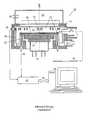
- FIG. 1illustrates a simplified cross-sectional view of a plasma-based manufacturing process chamber comprising sensor apparatus in accordance with one embodiment of the invention.
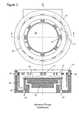
- FIG. 2depicts sensor apparatus in accordance with an embodiment of the invention that includes an array of dual floating Langmuir probes disposed about various components of the plasma chamber.
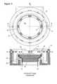
- FIG. 3depicts sensor apparatus in accordance with an embodiment of the invention that includes an array of dual floating Langrnuir probes disposed about the plasma chamber and upon a wafer holder that is capable of being electrically biased.
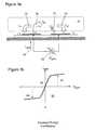
- FIG. 4illustrates a dual floating probe (DFP) structure, with a typical current-voltage response curve when exposed to a plasma and voltage bias signal.
- DFPdual floating probe
- FIG. 5is a schematic representation of a circuit for obtaining plasma currents from DFP sensors in accordance with some embodiments of the invention, and a typical current response of the sensors.
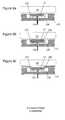
- FIG. 6 ais a cross section of a DFP device fabricated from a conductive electrode.
- FIG. 6 bis a cross section of a DFP device fabricated from an electrode and having an insulating surface or a deposited electrically insulating coating or film.
- FIG. 6 cis a cross section of a DFP device fabricated from an electrode and masked to control the line-of-sight deposition of sputtered or ion-beam deposited coatings or films.
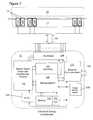
- FIG. 7illustrates a schematic electrical architecture of an embodiment of the invention in which the DFP sensors are multiplexed to a central pulse circuit, a data acquisition circuit, microprocessor, memory, power supply system and external communications.
- FIG. 8illustrates a matrix of current measurements made with near-zone DFP pairs and far-zone DFP pairs as sampled about the sensor array.
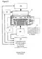
- FIG. 9illustrates a wafer plasma processing system in accordance with an embodiment of the invention wherein conditioned DFP sensor signals are used to monitor or control the plasma state.
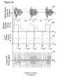
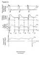
- FIG. 10illustrates typical waveforms from a pulsed RF plasma processing system in accordance with an embodiment of the invention showing dynamics of plasma properties that can be measured by synchronous sampling of DFP sensors within the pulse period.
- FIG. 11illustrates typical waveforms from a pulsed DC plasma processing system in accordance with an embodiment of the invention showing plasma properties that can be measured by synchronous sampling of DFP sensors.
- FIG. 12illustrates examples of trigger or gating signals in pulsed RF or pulsed DC plasma systems in accordance with an embodiment of the invention for the purposes of making synchronous measurements.
- FIG. 13illustrates a plasma processing system in accordance with an embodiment of the invention wherein conditioned DFP signals are used to monitor or control a magnetron sputtering reactive deposition process.
- FIG. 1illustrates one embodiment of an apparatus 10 that is capable of making real-time measurements of incident plasma current fluxes through arrays 12 of dual floating Langmuir probe (DFP) sensors 11 about the internal boundaries of a plasma processing system 14 .
- DFPLangmuir probe
- two sensor arrays 12are shown, with one array of DFP sensors disposed along the chamber liner 18 , and a second array of DFP sensors disposed along the so-called “focus ring” or dielectric isolation ring 20 .
- the processing systemis 14 comprised of a vacuum processing chamber 16 , a pumping manifold 22 , a plasma source 24 mounted to the top of or in communication with the vacuum chamber 16 , a gas delivery manifold or gas shroud (not shown), gas flow, thermal management and power services 28 connecting to the plasma source and system, and a wafer or workpiece chuck or mounting stage 30 .
- the workpiece chuckmay include a clamping means, RF power, fluid coolant, lifting pin assembly, and helium backside-thermal conduction facilities 32 .
- the sensors of the apparatus 10may be used with or without the wafer or workpiece 36 actually present within the processing chamber 16 .
- the outputs 38 and 40 of the DFP sensor arraysare connected to an external electronic subsystem 42 that houses the stimulating electronics, multiplexer, data acquisition and microprocessor controls for the apparatus.
- the output 44 of the electronic subsystem 42is then communicated to a central processor or computer 46 . Since the DPF sensor apparatus can be operated during an actual process, the central processor or computer 46 can use the data from the apparatus to monitoring the process conditions and to provide real-time feedback and control signals to various inputs to the plasma processing system.
- the electronic subsystem 42may be a separate box, a special micro-electronics add-in card associated with another piece of electronic hardware or computer 48 .
- the apparatusWhen a low-pressure ( ⁇ 100 Torr) gaseous discharge or plasma 50 is ignited within the processing chamber, the apparatus is used to sense the DFP currents which flow between local DFP sensor pad pairs 11 or, alternatively, the DFP currents that flow between non-local pairs within any combination amid sensor array assemblies 12 about the inner chamber 16 .
- the DFP sensors 11may be directly or capacitively coupled to the bipolar, pulsed excitation from the external electronics 42 and as such can be operated even when insulating coatings are deposited from the plasma process onto the surfaces of the DFP sensors.
- FIG. 2is a top view and cross sectional view illustrating an embodiment of a DFP sensor array 12 as disposed in the processing region of a plasma processing chamber 16 .
- a semiconductor wafer 36is disposed in process chamber 16 on a substrate chuck 30 .
- the plasma source (not shown) that powers and sustains the plasmamay be of any type, including DC plasma sources, DC- or RF-excited hollow cathode plasma sources, cathodic-arc plasma sources, magnetron sputtering sources, gridded or gridless broad-area ion sources, plasma sources operated with a capacitively driven electrodes, inductively coupled or ferrite-based inductively coupled plasma sources, electron cyclotron resonance microwave plasma sources, surface wave plasma sources, or RF helicon plasma sources.
- DC plasma sourcesDC- or RF-excited hollow cathode plasma sources
- cathodic-arc plasma sourcescathodic-arc plasma sources
- magnetron sputtering sourcesgridded or gridless broad-area ion sources
- plasma sources operated with a capacitively driven electrodesinductively coupled or ferrite-based inductively coupled plasma sources, electron cyclotron resonance microwave plasma sources, surface wave plasma sources, or RF helicon plasma sources.
- DFP arrays 12are shown disposed both on a chamber liner 18 as well as imbedded in the dielectric ring 20 that surrounds the substrate holder 30 .
- This ringis sometimes referred to as a “focus ring” in that it constrains the plasma properties and process gas flow dynamics about the edge of the wafer or workpiece.
- the DFP sensorshave electrically isolated, vacuum-sealed connections 38 and 40 that extend outside the vacuum chamber.
- the DFP probe connectionsmay incorporate passive RF resonant choke filtering elements (not shown) that are used to allow the probes 11 to follow any RF or AC field variations in a manner similar to any other floating surface on the liner 18 or focus ring 20 surfaces.
- any array of DFP sensors 12can be spatially configured about the interior chamber boundary, although it is preferred that the DFP sensors are in reasonable proximity to either the plasma source (or plasma body) and to the wafer or workpiece 36 being treated within the plasma processing chamber 16 .
- FIG. 3Another embodiment in accordance with the invention is shown in FIG. 3 , wherein one sensor array 12 is incorporated into the chuck or holder 30 of the wafer or workpiece 36 .
- Connections 52 to the DFP array on the chuck 30are routed through the chuck body.
- adequate RF filteringpreferably RF-resonant chokes and low-pass filtering
- FIG. 3also shows a secondary DFP array on the chamber liner 18 that may be used in tandem with the array disposed on the wafer or workpiece chuck.
- Plasma parameterssuch as ion current flux, charged particle density, electron energies (or apparent electron temperatures) and ion energies are physical parameters of the plasma that directly influence rates and quality of surface modification, deposition or etching.
- the dual floating Langmuir probeis used to collect physical parameters of the plasma.
- the DFPallows measurement of current and voltage ( 1 -V) characteristics of a plasma between two conductive probes that are allowed to electrically float apart from an electrical common or ground.
- FIGS. 4 a and 4 billustrate the basic working principles of a single DFP sensor.
- Two planar conductive probes 13are exposed to plasma 50 .
- a floating bias potential 62is induced between the probes to force a net current 64 through the plasma and DFP sensor circuit.
- the net DFP currentis limited by ion current flux 70 to the negatively biased probe surface due to the rejection of electron current 72 to the probe; this is known as the ion saturation current.
- the ion current 74 and electron current 76 to the second probecompensate such that all plasma currents sum to zero to satisfy the floating condition of the probe.
- an I-V trace 80is produced.
- the I-V trace of a typical DFP probehas characteristics similar to that of a back-to-back diode pair.
- the saturating currents 82 and 84correspond to ion saturation currents 70 and 74 respectively.
- the intermediate region of the I-V curve 86is determined by the electron currents 72 and 76 and may be used to determine the apparent electron temperature, ⁇ T c >, which is indicative of “high-energy” electron population of the electron energy distribution as manifested at the face of the DFP sensor pads 13 .
- Equation 1may be modified to take into account non-ideal situations that include effective probe area expansion with increasing bias potential, asymmetric probe areas, non-uniform plasmas and non-Maxwellian electron energy distributions.
- the conventional analysis that results in Eq. 1is for a DC floating DFP case, but is also applicable plasma environments where strong RF fields are present and where RF filtering is employed to allow the DFP sensor to follow the RF potential fluctuations inherent in the process.
- FIG. 5One example is illustrated in FIG. 5 , wherein the DFP sensor pads 13 are powered with a bipolar, square-wave pulsed power source 90 .
- the actual probe facesmay be directly connected to the voltage source or may be capacitively coupled through isolation capacitors 92 and 94 .
- the series capacitors 92 and 94are optional if the square wave pulsing supply is floating.
- These capacitive elementsmay also represent any dielectric layer that may appear on the probe surface, as for example in the form of a deposited dielectric film or an anodization coating.
- series RF resonant choke filters 96 and 98i.e. a series of tuned parallel capacitor-inductor elements in series with a low pass filter
- a common mode choke 100may be included to block any noise between the leads of the floating sensor.
- the DFP sensor pads 13can be stimulated with a bipolar pulsed signal 90 having a controlled peak-to-peak amplitude.
- the DFP sensorprovides a current 102 through the plasma 50 that can be sensed as a voltage 104 through across a sampling resistor 106 , or alternatively with an emitting diode.
- the excitation voltage level 108can be sampled as well.
- the pulsed excitationcan provide a high frequency current component 110 associated with a non-zero shunt capacitance 112 that is related to any parallel parasitic capacitance between the DFP sensor faces or electrical leads. In general it is preferred to keep the shunt capacitance small.
- the DFP sensor current 102can be resolved from the total current 114 . With appropriate methods of delay, sampling and holding, it is possible then to read the DFP ion saturation current value, even in cases where a thin dielectric coating appears on the surfaces of the DFP sensor pads. Moreover, if the level of the DFP sensor excitation voltage is controlled, it is possible to resolve the I-V characteristics of the DFP sensor, and thereby sense apparent electron temperature levels.
- the DFP sensordevelops a dielectric coating that has a net series capacitance value similar to or lower than the shunt capacitance, it becomes more difficult to separate the shunt current from the DFP sensor current.
- the probe faces or array assemblybe removable from the processing chamber and that they be fashioned from materials compatible with conventional chamber cleaning methods. For example, in PE-CVD processes that involve the deposition of carbon or silicon, it is helpful to have the DFP probes fabricated from materials that can be cleaned with oxygen- or fluorine-based chemistries, respectively.
- FIGS. 6 a , 6 b , and 6 cshow various configurations of DFP sensor pads.
- FIG. 6 ashows a single DFP sensor pad 13 that incorporates a substantially planar probe of about 0.1 to 10 cm 2 in area.
- the probeis electrically isolated from any conductive or anodized boundary on the chamber walls, liner or workpiece chuck as represented by 118 in this illustration.
- the probe sensormay also include insulators 120 and vacuum gaps 122 that separate the probe spatially from boundary surfaces. The gaps prevent the floating sensor from becoming grounded or capacitively coupled to other conductive boundaries when operating in depositing processes. Gap widths are typically on the order of 1 to 10 Debye lengths of the plasma in proximity to the probe (typically about 0.1 to 1 mm for applicable process conditions).
- FIG. 6 bshows the same DPF sensor pad 13 manufactured from a conductive electrode that has a dielectric or anodized layer 126 as may commonly be required in etching or chamber cleaning processes.
- the DFP sensorincludes a forward masking assembly 130 which prevents build up of sputtered, conductive coatings. Without the mask, conductive coatings could build up in the isolation gap and over the surface of the insulator, eventually causing the floating DFP sensor to be shorted to another conductive boundary or cause the collecting area of the planar DFP sensor pad to expand and lead to significant errors in the DFP measurements.
- an external electronic system 42is required to provide the probe bias over the array and collect the various DFP currents.
- the external circuitincludes a central microprocessor with AID sampling capability 140 , a bipolar-pulsed supply with DFP probe signal conditioning circuit 142 , a multiplexer 144 , and DC power source 146 and DC-DC converter 148 that condition the input power to the various components in the circuitry.
- Other componentsinclude memory 150 , internal clock 152 , and external communication electronics 154 .
- the multiplexed circuitryis used to direct the bipolar pulse waveform through wired connections 156 to the appropriate combination of DFP sensor pads 13 on the array 12 .
- External communications with the communication electronics 154may be by wired or wireless means.
- the microprocessordetermines when the A/D conversion is performed to avoid high frequency transient errors due to shunt capacitance and to provide sampling and averaging of the DFP currents and bias voltage signals.
- the circuitry in FIG. 7does not illustrate the optional common mode chokes, RF filters or isolation capacitors in line with connections 156 that have been described in FIG. 5 in connection with one embodiment of the invention.
- FIG. 8shows a matrix of DFP signal data 170 that can be collected by the sensor apparatus of the present invention.
- the off-diagonal currents, I i,j, 174 and 176could be similarly averaged ion saturation current terms associated with a non-local DFP sensor probes amid the array.
- the arraycould also hold effective electron temperature data as reduced from I-V data when the pulse amplitude of V bias is made relatively small.
- Mathematical and statistical treatment of the array of current terms 170can provide sensitive information about the state of the plasma at its boundary and, to a lesser degree, about the bulk conductance of the plasma body.
- feedback informationmay be used to control the set-point of delivered power into the process.
- the information taken from multiple DFP I-V sensorsmay be analyzed through one of many information processing architectures.
- One source of informationconsists of the matrix of readings from all of the I-V probes 170 . As described earlier, this is a square matrix of M ⁇ M rank where M is the number of probes.
- the diagonal terms 172are the measurements of each individual probe sensor and the off-diagonal terms 174 and 176 are the passive measurement at the i th probe from active pulsing of the j th probe.
- the structure of this matrixmay be analyzed by several decomposition techniques such as Cholesky, fractional, QR, Schmidt, triangular, or UD factorizations.
- singular value decompositionis another technique used to derive eigenvectors and the covariance matrices. This analysis serves as a fingerprint of the process and used to estimate hidden states of the process and plasma. This technique provides a snapshot in time of plasma conditions.
- Another construct of the probe datais in an N ⁇ M matrix where M is the number of probes and N is the number of temporal data values for each of the M probes.
- This vector-valued time seriesis analyzed using typical subspace projection methods common in control engineering applications.
- the analyses of these signalscan also be extended to constructs based on feedback-free exogenous signals that are used in closed-loop control of the process and in developing estimators for unobserved state variables. Extended Kalman filters and nonlinear estimators and filters may also be used to process the data from the matrix of I-V probe readings.
- the arraycan be of any dimension with the other vectors being time, excitation voltage, current polarity and the like.
- the apparatusprovides process real-time information that can be used to track the state of the plasma dynamically as it may be influenced by process events such as pressure bursts, flow controller over-shooting, transient imbalances of the plasma chemistry, and drifts in net power delivery due to deposition and build-up of coatings and films. Tracking and adjusting for such effects can be realized with the information gathered by the in-situ sensor devices in order to improve run-to-run performance, process adaptation and optimization and troubleshooting of problematic systems, with the goal of increasing product yield and process system up-time.
- process eventssuch as pressure bursts, flow controller over-shooting, transient imbalances of the plasma chemistry, and drifts in net power delivery due to deposition and build-up of coatings and films. Tracking and adjusting for such effects can be realized with the information gathered by the in-situ sensor devices in order to improve run-to-run performance, process adaptation and optimization and troubleshooting of problematic systems, with the goal of increasing product yield and process system up-time.
- FIG. 9illustrates use of sensor signals to monitor or control the plasma state in a wafer plasma processing system in accordance with an embodiment of the invention.
- a plasma processing system 10 used to process integrated circuit wafers 36comprises sensor arrays 12 .
- An electronic subsystem 42is provided to process the signals collected from the sensor arrays 12 into sensory feedback information on the boundary state of the plasma, which is furnished in turn to a system controller or electronic data server 180 .
- the processing of the sensory input signalsmay be accomplished in real time.
- the system controller 180uses the feedback information of the invention to adjust input levels of power to the plasma source 182 , gas flow levels to the systems mass flow controllers 184 , or power and bias levels to the wafer chuck sub-system 186 .
- controllers or factors affected by the controllermay include the pressure controller and pumping system and dynamic times of the process steps.
- processing electronics 42are shown as a separate electrical entity in FIG. 9 , these electronics may alternatively be mechanically combined in part or in total within the features of the system controller (or electronic data server) 180 or configured within the plasma source or wafer chuck subsystem power supply electronics.
- the DFP sensorsprovide very low perturbation of the plasma properties when activated and constructed properly.
- the sensorsWhen inactive, the sensors electrically charge to the floating potential as with other dielectrically isolated or anodized surfaces about the process chamber walls.
- the probesProvided that the probes have a low profile and smooth edges, the probe cannot act as an electrical boundary that would trap large or dusty charged particles which might lead to particle defects in semiconductor, memory or optical product processing.
- the total energy injected into the plasmais very small.
- the plasma densitywould be on the order of 10 11 cm ⁇ 3 and ion saturation current densities of about 1 mA/cm 2 .
- an effective pulsed-bias of about +/ ⁇ 40 V at the DFP sensorwith a pulsed on-time of about 0.5 msec at a duty cycle of 20% for DFP sensor areas of about 2.5 cm 2 .
- this conditionimplies a maximum power density of about of 10-20 mW.
- the DFP sensing apparatusaffords negligible impact on the plasma-based process while yielding real-time in-situ sensory information about the plasma body to aid in monitoring or controlling aspects of the plasma process conditions.
- the DFP arrayshave been represented as comprised of sensors having a pair of similar floating planar sensor pads which in principle have a bipolar current waveform in which I sat of probe 1 is about equal in magnitude to I sat of probe 2 or any other probe disposed symmetrically about the plasma chamber boundaries.
- an alternative variation on this apparatusis to have an array of single DFP sensor pads with a common electron return current pad.
- the common padneed not be of equal area of similar mechanical build, as the array of probe sensor pads and the pulsed-signal electronics would be unipolar with additional switching that would allows the pulse circuit to de-charge and re-trigger for each pulsed excitation.
- This configurationwhile somewhat more simple to implement, would provide an array of current terms that would only fill in the diagonal of the current matrix 170 of FIG. 8 .
- the present inventionmay also be utilized in plasma processing systems that employ pulsed RF or pulsed DC power operation.
- the sensor arrays of the inventionare used in pulsed power plasma systems, it is desirable to synchronize the acquisition of data from the sensors with the pulsing dynamics of the plasma processing system. This synchronization is advantageous since the application of pulsed operation induces periodic changes in the charged particle dynamics in the plasma processing system. Without synchronous sampling, the discrete or time-averaged sensor readings would have noise from being aliased against the pulsed power. Also, by using synchronous gating and sampling methods to obtain data within pulsed power applications, estimates of the plasma properties, such as ion saturation current and effective electron energy, can be characterized throughout the pulse period.
- FIG. 10illustrates an embodiment of the invention adapted to measure plasma properties in a pulsed RF power plasma processing system.
- the plasmaFor an RF power waveform envelope 200 typical of that observed during pulsed RF operation, the plasma exhibits time-varying characteristics of effective electron energy 202 and ion saturation current 204 .
- the pulsing frequency of a pulsed RF plasma processing systemis typically in the range of about 100 Hz to about 10 kHz, which is less than the preferred excitation frequency of a pulsed DFP sensor of between 1 to 20 kHz.
- ion saturation current as measured by a DFP sensor excited with a bipolar pulsewould be observed as a signal envelope 206 .
- synchronous sampling of plasma properties throughout the plasma pulse periodmay be obtained and used to develop dynamic or time-averaged values of the plasma properties.
- noise in the collected sensor readings due to aliasing against the power pulsingis avoided, thus making the readings more representative of the true temporal dynamics of the plasma state.
- FIG. 11illustrates an embodiment of the invention adapted for use in a pulsed-DC plasma processing system, such as those employed for magnetron sputtering or in broad area ion sources.
- the pulsed DC potential 210is switched briefly from a relatively large negative potential to a reverse potential (i.e. slightly positive), as for example to “de-charge” periodically the cathode surface of the DC plasma source.
- a reverse potentiali.e. slightly positive
- the plasma of the systemexhibits time-varying characteristics of effective electron energy 212 and ion saturation current 214 .
- the pulsing frequencymay be anywhere in the range of 20 kHz to 400 kHz, which is typically much higher than the preferred excitation frequency of a pulsed DFP sensor.
- the dynamic response of the plasma propertiesare replicated several times within one pulsed DFP time period as shown in waveform 216 .
- sampling of the sensor signalsmay be synchronized with features of the pulsed-DC power waveform. In this way, sensor readings may be collected that are less prone to noise and more representative of the true temporal dynamics of the plasma state.
- any number of external signalsmay be available for triggering or gating synchronous sampling of the sensors of the invention.
- external current and voltage signals 220from the plasma source apparatus, or from anywhere between the power supply and plasma source, are employed to synchronize sampling of the sensors. Signals representative of the optical emission intensity of the plasma may also be employed.
- power “ON/OFF” signals or “ ⁇ DC/+DC” signals 222available from the internal control circuitry or user interface of the power supply are used to synchronize triggering or gating of the sensors.
- Yet another alternativeis to sense a signal from the pulse-powered plasma itself by means of an independent floating probe 224 that is in contact with the plasma body.
- the independent floating probe sensormay be included as part of a sensor array assembly of the invention.
- the external signalscan communicate the pulsing event to the sensor array processing circuitry 42 through a signal conditioner, isolator or buffer 226 , for synchronous sampling of the sensor array signals. Synchronous sampling is achieved in these examples by combining the one or more external signals representative of the power pulsing event with a pulse signal from the pulsed sensor array system in order to properly gate the data acquisition from the sensor array.
- FIG. 13An embodiment of the invention employed in a reactive sputter deposition process is shown in FIG. 13 .
- the plasma source 24is a magnetron sputtering source used to deposit reactive coatings or films in the process system 10 on workpiece 36 . Since magnetron sputtering systems are, by nature, multivariable, it is desirable to use the plasma sensory signals as a means to monitor and control the state of the deposition process. To this end, ion saturation current and electron temperature measurements from one or more DFP sensor arrays 12 are taken in real time from electronics 42 . Alternatively, signals from other types of sensors described in accordance with the invention may be employed.
- the real-time measurementsare provided as a series of feedback signals 230 to other subsystems through a multivariable input-output control module 180 , as described above in connection with the embodiment depicted in FIG. 9 .
- the sensory signalsact as state estimators for the purpose of real-time control.
- the ion saturation current state estimator or estimatorswould provide feedback to the magnetron power supply 182 , total flow levels within the flow control module 184 , and pressure/pumping subsystem 232 , since it is known that mean or dynamic measurements of ion saturation current are largely dependent upon power, pressure and flow settings.
- a state estimator of electron temperaturecould be fed back to the flow control sub-system 184 so as to adjust further the ratio of neutral gas (e.g. Ar) to reactive gas (e.g. O 2 or N 2 ), as well as the partial pressure of the reactive gas.
- neutral gase.g. Ar
- reactive gase.g. O 2 or N 2
- the process input parameterssuch as power, pressure, and gas flow rates, can be adjusted in real time to ensure that the process is more accurately targeted and made repeatable in production.
- the inventioncan be applied to either reactive or metal sputtering processes (batch or in-line) configured for either single or multiple sputter cathode target materials or sputtering zones.
- a sensor array of the inventionmay comprise photo sensors for measuring plasma optical emission spectroscopy and particle light scattering.
- This sensorincludes any form of optically filtered semiconductor photo sensor that can discriminate the intensity of the plasma light emission over selected bandwidths associated with various excited states of molecular and atomic species within the gas discharge or plasma.
- actinometrymay be quantified, etch end-point events may be detected, or the state of the reactive gas chemistries in plasma assisted chemical vapor deposition processes may be examined.
- Multiple sensorsmay be deployed in an array in order to measure the intensity of different spectra and compact lenses or occluding optics may also be used to collect line-integrated light from a narrow angle, thereby allowing computation of information on the volumetric spatial structure of the plasma emission intensity.
- Components for optical emissionare commercially available including pre-packaged narrow band-pass filtered photo-detectors, photo array detectors with wedge filter assemblies, and broadband spectral emissions sensors that have been integrated into a single IC package.
- a photo detector arrayYet another application of a photo detector array is the detection of light scattered from charged particulates suspended in the plasma or from particulates that have been deposited on the workpiece. These particulates can cause defects and yield problems in IC fabrication, memory media and in high performance optical coatings.
- a source of lightsuch as an intense LED (with focusing optics) is directed through the plasma across the substrate (i.e. near the plasma sheath over the substrate) or at an incident angle onto surface of the substrate.
- the intensity of reflected light or scattered lightis detected by the photo detector array, distributed at various angles, in order to quantify the level of particulate formation within the plasma on the substrate during processing.
- the inventionmay also employ photo sensors for absorption spectroscopy.
- This sensoris a combination of a light source, such as an infrared light emitting diode, and a receiving photo detector, which may include narrow band-pass filtering.
- a matching set of light-source and photo-detector componentsare disposed on opposite sides of the array so as to detect the line-of-sight photo-absorption level of the select gases within in the processing system. Since the absorption level is proportional to line of site integrated gas species concentration, the sensor can be used to quantify bulk concentrations of various gas components in the processing system.
- the photo-absorption sensor arraymay be used to deduce reactive gas or gaseous by-product concentration profiles within the bulk of the system. Examples of important gas species that may be monitored in this manner include SF 6 , various C x F y species, and SiF 4 , which is typically an etch or chamber-clean byproduct.
- the inventionmay also employ thermal sensors for wall temperature and surface temperature chemical catalytic sensing.
- Wall temperatures within a processing systemare dependent upon various forms of power flux including radiative heat, gas conduction, plasma light emission, charge particle flux and de-excitation and chemical reactivity and upon the thermal mass, as well as thermal management of process chamber walls or liners. Since the sensor array is part of the processing system boundary, temperature sensors may be used to monitor wall temperature dynamics, repeatability and variance. In some instances temperature sensor may be needed to serve another sensor component or sampling electronics to as a means for thermal compensation for accurate measurements.
- Thermal sensorsmay also be used in surface catalytic measurements to monitor the relative flux, concentration, or transport of select reactive gas species. For example, the relative concentrations or surface flux of atomic hydrogen or atomic oxygen may be quantified with an array of thermal-catalytic sensors. By fabricating a thermal probe from (or coating the probe with) a specific catalytic material, the thermal energy received by the probe is related to catalytic recombination of these reactive atomic species. Secondary thermal sensors without the catalytic material may also be provided in order to de-couple effects of conductive or radiative heating from that due to the heat of the catalytic surface reaction.
- surface acoustic wave sensorsare employed for measuring pressure, film thickness and deposition rates.
- Pressureis an important physical parameter within plasma processing systems in that it relates to the total concentration of gases and gas temperature. Typically, pressure is monitored only at the boundary of the process chamber at a single point.
- an array of sensors for measuring pressureis used for monitoring or controlling the state of the processing system and assists in monitoring subtle spatial variation in gas pressure that result in non-uniformity of the process.
- An example of one type of compact pressure sensor that may be used in a sensor array of the inventionis a surface acoustic wave sensor or “SAW” device, as described for example in Draft, “Acoustic Wave Sensor Technology Sensors,” Sensors , January 2001.
- SAWsurface acoustic wave sensor
- TSMthickness shear mode
- the response of piezoelectric deviceis sensitive to the build-up of any mass disposed upon its surface.
- Such sensorshave commonly been used in the vacuum coating industry for measuring deposition rates and total film thicknesses.
- an array of TSM-SAW devicesmay be used to monitor the rate of deposition of materials about the process chamber wall.
- SAW devicescan be made very sensitive to changes in mass, they may also be used in detecting co-deposition of residual films that may build up during etching processes, or for detecting the existence of unwanted particles that may have been generated within the process.
- Such sensorsmay be used to monitor deposition process in real time, or to aid in determining when a chamber has been appropriately pre-seasoned or should be scheduled for preventative maintenance.
- MEMsmicro-electromechanical system
- MEMs-based accelerometeruseful for measuring the mechanical vibrations about the plasma processing system.
- These micro-accelerometersprovide information associated with the integrity of mechanical components or subsystems (e.g. turbo-pumps, gate valves, robotics, lift assemblies) to detect the presence of excessive loading or wear, increased friction, shock and mechanical vibration. This information may be used to trigger preventative maintenance action before mechanical failure, or to aid in tracing particle contamination problems to mechanical wear or mechanical disturbances induced by the user or external environment.
- MEMs sensorthat may be used in the present invention is a select gas concentration sensor.
- CMOS MEMs resonant beam gas sensoras described for example in Hagleitner et al., “A Single-Chip CMOS Resonant Beam Gas Sensor,” 2001 IEEE International Solid-State Circuits Conference, Feb. 6, 2001.
- an oscillated, chemically sensitive cantilever beamis used to detect concentrations of select gases absorbed on the beam's surface.
- An array of such sensors about the walls of a chambermay be used to determine net diffusive concentrations of various gases in non-depositing processes.
Landscapes
- Engineering & Computer Science (AREA)
- Physics & Mathematics (AREA)
- Plasma & Fusion (AREA)
- Chemical & Material Sciences (AREA)
- Analytical Chemistry (AREA)
- General Physics & Mathematics (AREA)
- Condensed Matter Physics & Semiconductors (AREA)
- Manufacturing & Machinery (AREA)
- Computer Hardware Design (AREA)
- Microelectronics & Electronic Packaging (AREA)
- Power Engineering (AREA)
- Plasma Technology (AREA)
- Drying Of Semiconductors (AREA)
- Chemical Vapour Deposition (AREA)
- Physical Vapour Deposition (AREA)
Abstract
Description
- 1. Field of the Invention
- This invention relates generally to plasma processing systems, and more particularly to apparatus and methods for making in-situ measurements of plasma properties in plasma processing systems.
- 2. Brief Description of the Prior Art
- Single-ended Langmuir probes and other diagnostic probe methods have been widely used in industry to characterize plasmas, and more specifically plasmas used in low pressure vacuum processing systems. Measurement techniques have been described in reference books including Swift and Schwar,Electric Probes for Plasma Diagnostics, (American Elsevier, New York, 1969) and by Hershkowitz inPlasma Diagnostic, Vol.1,Discharge Parameters and Chemistry, ed. Aucciello and Flamm (Academic, New York, 1989), pp. 113-183. The use of single-ended Langmuir probe diagnostic methods for monitoring plasma processing environments is also known, along with methods for operating the probes as generally needed for plasma characterization. For example, in U.S. Pat. No. 4,006,404, Szuszczewicz et al. discuss excitation of a single-ended Langmuir probe through pulsed modulation so as to avoid problems associated with sampling and surface contamination. In U.S. Pat. No. 5,339,039, Carlile et al. describe a single-ended Langmuir probe system that incorporates radio frequency (RF) compensation and tuned-filtering for operation in RF powered plasma environments. In U.S. Pat. No. 5,167,748, Hall describes using one or more single-ended Langmuir probes to measure charged particle density and electron temperature in order to monitor the state of the plasma and thereby control the plasma geometry within a processing system.
- More recently, diagnostic probe assemblies on various components of plasma-based processing systems, such as low pressure semiconductor processing chambers, have been described. Exemplary of this work is U.S. Pat. No. 5,451,784 to Loewenhardt et al., wherein plasma probes and ion energy analyzers are include on a composite diagnostic wafer that is then disposed into a plasma processing system in order to characterize the plasma properties adjacent to the workpiece surface. Similarly, Ke et al. in U.S. Pat. No. 5,989,349 describe the use of planar probes embedded in a semiconductor wafer process diagnostic pedestal for the purpose of monitoring ion currents from the plasma and DC bias potentials. Hikosaka, et al. in U.S. Pat. No. 5,471,115, describe a method for measuring plasma properties using a high frequency plasma oscillation probe that measures absolute electron density in the plasma, with the intent to feed such information back to a main control system that can adjust RF power, gas flows or operating pressure. Also, Booth et al. in U.S. Pat. No. 5,936,413 describe using a capacitively isolated, single-ended planar probe that is excited with an RF voltage waveform to obtain plasma characteristics while avoiding deposition and probe surface contamination and disruption of the processing plasma.
- All of the techniques described above have limitations that restrict their usefulness in obtaining real-time measurements of plasma conditions within commercial plasma processing systems. Many of these measuring devices are intrusive in that they require the use of a probe that protrudes into the plasma body, which inherently disrupts the plasma properties when processing materials. Moreover, the use of any single-ended probe is intrusive, particularly when the probe is forward biased at or near the plasma potential, resulting in a condition that necessarily disrupts the electrical structure of the plasma body during processing. Many of the techniques described are intended for experimental characterization of non-corrosive or non-depositing plasmas, and are thus not intended to collect plasma measurements under commercial processing conditions. Finally, these teachings typically provide only a single-point approach to monitoring the plasma properties, and as such provide no means of determining the global or spatial properties of the processing plasma at its boundary.
- This invention provides apparatus and methods for making in-situ measurements of plasma properties in plasma processing systems. The diagnostic apparatus is virtually non-invasive, and can be configured to serve a broad range of needs for monitoring the properties of processing plasmas and to provide data on those properties in a manner required for process control. The apparatus generally comprises a physical sensor array disposed within a plasma processing chamber, an electrical circuit for stimulating the sensors, and means for recording and communicating sensor measurements for monitoring or control of the plasma process.
- In one embodiment of the invention, an array of dual floating Langmuir probe (DFP) sensors is disposed within a plasma processing system. The DFP sensors measure incident charged particle currents and electron temperatures in proximity to the plasma boundary or boundaries within the processing system. The DFP sensors are electrostatically floated with respect to the plasma potential so as to cause minimal perturbation of the plasma medium. As a result, the measurement apparatus is non-invasive to the plasma process. Sensor arrays of the invention may also comprise, for example, optical sensors for measuring plasma optical emission spectroscopy and particle light scattering; photo sensors for absorption spectroscopy; thermal sensors for wall temperature and surface temperature chemical catalytic sensing; surface acoustic wave sensors for measuring pressure, film thickness and deposition rates; and micro-electromechanical systems for tactile chemical sensing, mass spectrometry, ion energy and vibration measurements.
- In one embodiment of the invention, the diagnostic sensors are disposed along a portion of the chamber liner of a vacuum processing system. In other embodiments, the sensor array may be disposed about the dielectric isolation ring (or “focus ring”) of the chamber, a gas injection ring, or upon a portion of a substrate holder or “chuck.” The sensors may also be disposed within the wall of the chamber. The sensor devices may be made removable and separable from driving electronics and electrical feed-throughs for servicing or replacement.
- By utilizing an array of sensors, the invention provides an ability to obtain diagnostic data, such as ion current flux and effective electron temperature, from multiple locations about the boundary of the plasma body. The invention also provides an ability to monitor boundary properties of a processing plasma about multiple boundaries of the plasma body. In this way, the invention provides for acquiring data that may be used to deduce the global or spatial properties of the plasma, and variations in those properties, in order to monitor and control the process.
- The diagnostic sensors of the invention are suitable for use in plasma processing systems where either a protective layer is required within the chamber to inhibit corrosive chemical attack, as would typically be the case in an etching process, or where optically opaque or electrically insulating films or coatings are formed, as in a deposition process. Even with the presence of a dielectric layer atop the sensors, in the form of a coating or deposited film, the sensors remain capacitively coupled to the electrical environment of the plasma when taking measurements of the plasma properties. The invention may thus be adapted for use in a variety of plasma processing systems, including systems used for etching, plasma-enhanced chemical vapor deposition, reactive sputter deposition and conductive sputter deposition.
- In one embodiment of the invention, a multi-channel (multiplexed) circuit provides electrical stimuli to the sensors of the array. The sensors may be driven by various alternating excitation waveforms, such as a sinusoid signal, a bipolar pulsed-signal, or a small amplitude saw-tooth signal. The sensors may be stimulated directly or through a capacitive or transformer-isolated electrical connection. Embodiments of the invention also include means of controlling the multiplexing of the sensors, and of filtering out unwanted RF signals that originate from the plasma which might otherwise distort the diagnostic measurements.
- The invention also provides an ability to obtain diagnostic data in plasma processing systems that use pulsed RF or pulsed DC power. In one embodiment of the invention, stimulation of and acquisition of data from the sensors is linked or gated to the periodic pulsing of an RF power supply powering the plasma. Measurements of plasma properties may be acquired during both the on-time and off-time of the RF pulses. In this manner, for example, time constants of the plasma source system, such as charged particle density rise and decay times, may be deduced. In another embodiment of the invention, the stimulation and reading of the sensors is linked or gated to the periodic pulsing of a DC power supply powering the plasma. In this instance, the measurements may be acquired during the “−DC on-time” or the “+DC reverse-time” commonly associated with DC-pulsed plasma operation. For both pulsed RF and pulsed DC systems, the dynamics of charged particle density, apparent electron energy and various plasma system time constants may be sensed.
- The sensor arrays and other apparatus of the invention are useful for making measurements of sufficient speed and sensitivity to monitor the state of the process plasma in real-time, and to enable sensory feedback for control of the plasma processing system and its subsystems. In one method provided by the invention, signals from a sensor array are recorded and stored as a matrix, with each element of the matrix representing information associated with particular sensor pairs of the array. The matrix of terms may then be evaluated to determine spatial properties of the plasma as may be required to provide real-time monitoring of the plasma process, or for real-time feedback through the action of an external control system.
- The present invention may have application in any type of low-pressure plasma-based processing system. Examples include any IC wafer processing system, a single or multiple memory disk coating system, an optical electronic processing system, a stationary or moving glass cleaning, etching or coating system, a web coating or surface treatment system, or any plasma processing system in which working gases or workpieces are treated by a plasma. Moreover, the present invention applies to processing systems whose function is to excite gases via a plasma that are disposed into the system or even for the purpose of producing radiative photonic emissions such as UV light.
FIG. 1 illustrates a simplified cross-sectional view of a plasma-based manufacturing process chamber comprising sensor apparatus in accordance with one embodiment of the invention.FIG. 2 depicts sensor apparatus in accordance with an embodiment of the invention that includes an array of dual floating Langmuir probes disposed about various components of the plasma chamber.FIG. 3 depicts sensor apparatus in accordance with an embodiment of the invention that includes an array of dual floating Langrnuir probes disposed about the plasma chamber and upon a wafer holder that is capable of being electrically biased.FIG. 4 illustrates a dual floating probe (DFP) structure, with a typical current-voltage response curve when exposed to a plasma and voltage bias signal.FIG. 5 is a schematic representation of a circuit for obtaining plasma currents from DFP sensors in accordance with some embodiments of the invention, and a typical current response of the sensors.FIG. 6 ais a cross section of a DFP device fabricated from a conductive electrode.FIG. 6 bis a cross section of a DFP device fabricated from an electrode and having an insulating surface or a deposited electrically insulating coating or film.FIG. 6 cis a cross section of a DFP device fabricated from an electrode and masked to control the line-of-sight deposition of sputtered or ion-beam deposited coatings or films.FIG. 7 illustrates a schematic electrical architecture of an embodiment of the invention in which the DFP sensors are multiplexed to a central pulse circuit, a data acquisition circuit, microprocessor, memory, power supply system and external communications.FIG. 8 illustrates a matrix of current measurements made with near-zone DFP pairs and far-zone DFP pairs as sampled about the sensor array.FIG. 9 illustrates a wafer plasma processing system in accordance with an embodiment of the invention wherein conditioned DFP sensor signals are used to monitor or control the plasma state.FIG. 10 illustrates typical waveforms from a pulsed RF plasma processing system in accordance with an embodiment of the invention showing dynamics of plasma properties that can be measured by synchronous sampling of DFP sensors within the pulse period.FIG. 11 illustrates typical waveforms from a pulsed DC plasma processing system in accordance with an embodiment of the invention showing plasma properties that can be measured by synchronous sampling of DFP sensors.FIG. 12 illustrates examples of trigger or gating signals in pulsed RF or pulsed DC plasma systems in accordance with an embodiment of the invention for the purposes of making synchronous measurements.FIG. 13 illustrates a plasma processing system in accordance with an embodiment of the invention wherein conditioned DFP signals are used to monitor or control a magnetron sputtering reactive deposition process.FIG. 1 illustrates one embodiment of anapparatus 10 that is capable of making real-time measurements of incident plasma current fluxes througharrays 12 of dual floating Langmuir probe (DFP)sensors 11 about the internal boundaries of aplasma processing system 14. In this particular illustration, twosensor arrays 12 are shown, with one array of DFP sensors disposed along thechamber liner 18, and a second array of DFP sensors disposed along the so-called “focus ring” ordielectric isolation ring 20. The processing system is14 comprised of avacuum processing chamber 16, a pumpingmanifold 22, aplasma source 24 mounted to the top of or in communication with thevacuum chamber 16, a gas delivery manifold or gas shroud (not shown), gas flow, thermal management andpower services 28 connecting to the plasma source and system, and a wafer or workpiece chuck or mountingstage 30. In the case of a semiconductor processing system, the workpiece chuck may include a clamping means, RF power, fluid coolant, lifting pin assembly, and helium backside-thermal conduction facilities 32. There may also be included a load lock transfer stage withmechanical robotics 34 to manipulate and position the wafer orworkpiece 36. In practice, the sensors of theapparatus 10 may be used with or without the wafer orworkpiece 36 actually present within theprocessing chamber 16.- The
outputs electronic subsystem 42 that houses the stimulating electronics, multiplexer, data acquisition and microprocessor controls for the apparatus. Theoutput 44 of theelectronic subsystem 42 is then communicated to a central processor orcomputer 46. Since the DPF sensor apparatus can be operated during an actual process, the central processor orcomputer 46 can use the data from the apparatus to monitoring the process conditions and to provide real-time feedback and control signals to various inputs to the plasma processing system. Theelectronic subsystem 42 may be a separate box, a special micro-electronics add-in card associated with another piece of electronic hardware or computer48. When a low-pressure (<100 Torr) gaseous discharge orplasma 50 is ignited within the processing chamber, the apparatus is used to sense the DFP currents which flow between local DFP sensor pad pairs11 or, alternatively, the DFP currents that flow between non-local pairs within any combination amidsensor array assemblies 12 about theinner chamber 16. As will be described, theDFP sensors 11 may be directly or capacitively coupled to the bipolar, pulsed excitation from theexternal electronics 42 and as such can be operated even when insulating coatings are deposited from the plasma process onto the surfaces of the DFP sensors. FIG. 2 is a top view and cross sectional view illustrating an embodiment of aDFP sensor array 12 as disposed in the processing region of aplasma processing chamber 16. InFIG. 2 , asemiconductor wafer 36 is disposed inprocess chamber 16 on asubstrate chuck 30. The plasma source (not shown) that powers and sustains the plasma may be of any type, including DC plasma sources, DC- or RF-excited hollow cathode plasma sources, cathodic-arc plasma sources, magnetron sputtering sources, gridded or gridless broad-area ion sources, plasma sources operated with a capacitively driven electrodes, inductively coupled or ferrite-based inductively coupled plasma sources, electron cyclotron resonance microwave plasma sources, surface wave plasma sources, or RF helicon plasma sources.- In the embodiment of
FIG. 2 ,DFP arrays 12 are shown disposed both on achamber liner 18 as well as imbedded in thedielectric ring 20 that surrounds thesubstrate holder 30. This ring is sometimes referred to as a “focus ring” in that it constrains the plasma properties and process gas flow dynamics about the edge of the wafer or workpiece. The DFP sensors have electrically isolated, vacuum-sealedconnections probes 11 to follow any RF or AC field variations in a manner similar to any other floating surface on theliner 18 orfocus ring 20 surfaces. In this manner, any array ofDFP sensors 12 can be spatially configured about the interior chamber boundary, although it is preferred that the DFP sensors are in reasonable proximity to either the plasma source (or plasma body) and to the wafer orworkpiece 36 being treated within theplasma processing chamber 16. - Another embodiment in accordance with the invention is shown in
FIG. 3 , wherein onesensor array 12 is incorporated into the chuck orholder 30 of the wafer orworkpiece 36.Connections 52 to the DFP array on thechuck 30 are routed through the chuck body. Provided that adequate RF filtering (preferably RF-resonant chokes and low-pass filtering) methods are appropriately integrated in-line with the connections to thearray 52, theDFP array 12 can function even when thewafer holder 30 is powered with an RF bias as is often required in various semiconductor or materials processing methods.FIG. 3 also shows a secondary DFP array on thechamber liner 18 that may be used in tandem with the array disposed on the wafer or workpiece chuck. - Knowledge of plasma parameters about the boundaries of the plasma body, and their spatial and temporal variations, is helpful in understanding the dynamics of plasma-based processes. Plasma parameters such as ion current flux, charged particle density, electron energies (or apparent electron temperatures) and ion energies are physical parameters of the plasma that directly influence rates and quality of surface modification, deposition or etching. In one embodiment of the invention, the dual floating Langmuir probe (DFP) is used to collect physical parameters of the plasma. The DFP allows measurement of current and voltage (1-V) characteristics of a plasma between two conductive probes that are allowed to electrically float apart from an electrical common or ground.
FIGS. 4 aand4billustrate the basic working principles of a single DFP sensor. Two planarconductive probes 13 are exposed toplasma 50. A floatingbias potential 62 is induced between the probes to force a net current64 through the plasma and DFP sensor circuit. When placed at relatively high bias potentials, the net DFP current is limited by ioncurrent flux 70 to the negatively biased probe surface due to the rejection of electron current72 to the probe; this is known as the ion saturation current. The ion current74 and electron current76 to the second probe compensate such that all plasma currents sum to zero to satisfy the floating condition of the probe. When the probes are nearly symmetric in geometry and the plasma has relatively uniform characteristics across the faces of the probe, anI-V trace 80 is produced. As seen inFIG. 4 b, the I-V trace of a typical DFP probe has characteristics similar to that of a back-to-back diode pair. The saturatingcurrents ion saturation currents - The intermediate region of the
I-V curve 86 is determined by theelectron currents DFP sensor pads 13. - The current characteristics versus bias voltage for a symmetric dual-floating probe is approximated by
where I+satis the ion saturation current, V0is the floating potential of the probes when no bias is applied, VDPFis the differentially applied probe voltage, and Teis the apparent electron temperature.Equation 1 may be modified to take into account non-ideal situations that include effective probe area expansion with increasing bias potential, asymmetric probe areas, non-uniform plasmas and non-Maxwellian electron energy distributions. The conventional analysis that results in Eq. 1 is for a DC floating DFP case, but is also applicable plasma environments where strong RF fields are present and where RF filtering is employed to allow the DFP sensor to follow the RF potential fluctuations inherent in the process. - To implement the DFP diagnostic technique on a practical in-situ sensor, it is necessary to provide a floating probe bias means. One example is illustrated in
FIG. 5 , wherein theDFP sensor pads 13 are powered with a bipolar, square-wave pulsedpower source 90. The actual probe faces may be directly connected to the voltage source or may be capacitively coupled throughisolation capacitors series capacitors common mode choke 100 may be included to block any noise between the leads of the floating sensor. - With the circuitry arrangement of
FIG. 5 , theDFP sensor pads 13 can be stimulated with a bipolarpulsed signal 90 having a controlled peak-to-peak amplitude. With this stimulus, the DFP sensor provides a current102 through theplasma 50 that can be sensed as avoltage 104 through across a sampling resistor106, or alternatively with an emitting diode. Theexcitation voltage level 108 can be sampled as well. The pulsed excitation can provide a high frequencycurrent component 110 associated with anon-zero shunt capacitance 112 that is related to any parallel parasitic capacitance between the DFP sensor faces or electrical leads. In general it is preferred to keep the shunt capacitance small. Provided that the values of anyisolation capacitances shunt capacitance 112, the DFP sensor current102 can be resolved from the total current114. With appropriate methods of delay, sampling and holding, it is possible then to read the DFP ion saturation current value, even in cases where a thin dielectric coating appears on the surfaces of the DFP sensor pads. Moreover, if the level of the DFP sensor excitation voltage is controlled, it is possible to resolve the I-V characteristics of the DFP sensor, and thereby sense apparent electron temperature levels. - For those cases where the DFP sensor develops a dielectric coating that has a net series capacitance value similar to or lower than the shunt capacitance, it becomes more difficult to separate the shunt current from the DFP sensor current. In processes where thick dielectric films build up on the probe faces, it may be necessary clean the probe face or remove it from the processing system. Thus, it is preferred that the probe faces or array assembly be removable from the processing chamber and that they be fashioned from materials compatible with conventional chamber cleaning methods. For example, in PE-CVD processes that involve the deposition of carbon or silicon, it is helpful to have the DFP probes fabricated from materials that can be cleaned with oxygen- or fluorine-based chemistries, respectively.
FIGS. 6 a,6b, and6cshow various configurations of DFP sensor pads.FIG. 6 ashows a singleDFP sensor pad 13 that incorporates a substantially planar probe of about 0.1 to 10 cm2in area. The probe is electrically isolated from any conductive or anodized boundary on the chamber walls, liner or workpiece chuck as represented by118 in this illustration. The probe sensor may also includeinsulators 120 andvacuum gaps 122 that separate the probe spatially from boundary surfaces. The gaps prevent the floating sensor from becoming grounded or capacitively coupled to other conductive boundaries when operating in depositing processes. Gap widths are typically on the order of 1 to 10 Debye lengths of the plasma in proximity to the probe (typically about 0.1 to 1 mm for applicable process conditions). Theelectrical connection 124 to thesensor pad 13 is located on the backside of the pad with mechanical features that allow the probe to be removed for servicing or replaced, if necessary.FIG. 6 bshows the sameDPF sensor pad 13 manufactured from a conductive electrode that has a dielectric oranodized layer 126 as may commonly be required in etching or chamber cleaning processes. InFIG. 6 c, the DFP sensor includes aforward masking assembly 130 which prevents build up of sputtered, conductive coatings. Without the mask, conductive coatings could build up in the isolation gap and over the surface of the insulator, eventually causing the floating DFP sensor to be shorted to another conductive boundary or cause the collecting area of the planar DFP sensor pad to expand and lead to significant errors in the DFP measurements.- In order to operate the DFP sensor, an external
electronic system 42 is required to provide the probe bias over the array and collect the various DFP currents. One example of the architecture of this circuitry is illustrated inFIG. 7 . In this example the external circuit includes a central microprocessor withAID sampling capability 140, a bipolar-pulsed supply with DFP probesignal conditioning circuit 142, amultiplexer 144, andDC power source 146 and DC-DC converter 148 that condition the input power to the various components in the circuitry. Other components includememory 150,internal clock 152, andexternal communication electronics 154. The multiplexed circuitry is used to direct the bipolar pulse waveform through wiredconnections 156 to the appropriate combination ofDFP sensor pads 13 on thearray 12. External communications with thecommunication electronics 154 may be by wired or wireless means. Against its own timing or gating, the microprocessor determines when the A/D conversion is performed to avoid high frequency transient errors due to shunt capacitance and to provide sampling and averaging of the DFP currents and bias voltage signals. Note that the circuitry inFIG. 7 does not illustrate the optional common mode chokes, RF filters or isolation capacitors in line withconnections 156 that have been described inFIG. 5 in connection with one embodiment of the invention. FIG. 8 shows a matrix ofDFP signal data 170 that can be collected by the sensor apparatus of the present invention. For example, each current term along the diagonal of the array, Ii,i,172 could represent the average of the ion saturation current amplitudes measured between a local pair of DFP probe sensor pads:
The off-diagonal currents, Ii,j,174 and176 could be similarly averaged ion saturation current terms associated with a non-local DFP sensor probes amid the array. These current terms hold additional information on the bulk state of the plasma body since the current stimulated between the probes are non-local and must conduct through a greater portion of the plasma body. Alternatively, the array could also hold effective electron temperature data as reduced from I-V data when the pulse amplitude of Vbiasis made relatively small.- Mathematical and statistical treatment of the array of
current terms 170 can provide sensitive information about the state of the plasma at its boundary and, to a lesser degree, about the bulk conductance of the plasma body. By correlating the output of the array of current terms to either simple or complex power balance models of the plasma, it is possible to use the apparatus to obtain feedback information for real-time process control. For example, feedback information may be used to control the set-point of delivered power into the process. To perform this function, the information taken from multiple DFP I-V sensors may be analyzed through one of many information processing architectures. One source of information consists of the matrix of readings from all of the I-V probes170. As described earlier, this is a square matrix of M×M rank where M is the number of probes. Thediagonal terms 172 are the measurements of each individual probe sensor and the off-diagonal terms - Another construct of the probe data is in an N×M matrix where M is the number of probes and N is the number of temporal data values for each of the M probes. This vector-valued time series is analyzed using typical subspace projection methods common in control engineering applications. The analyses of these signals can also be extended to constructs based on feedback-free exogenous signals that are used in closed-loop control of the process and in developing estimators for unobserved state variables. Extended Kalman filters and nonlinear estimators and filters may also be used to process the data from the matrix of I-V probe readings. The array can be of any dimension with the other vectors being time, excitation voltage, current polarity and the like.
- By combining the DFP array apparatus with information processing methods, the apparatus provides process real-time information that can be used to track the state of the plasma dynamically as it may be influenced by process events such as pressure bursts, flow controller over-shooting, transient imbalances of the plasma chemistry, and drifts in net power delivery due to deposition and build-up of coatings and films. Tracking and adjusting for such effects can be realized with the information gathered by the in-situ sensor devices in order to improve run-to-run performance, process adaptation and optimization and troubleshooting of problematic systems, with the goal of increasing product yield and process system up-time.
FIG. 9 illustrates use of sensor signals to monitor or control the plasma state in a wafer plasma processing system in accordance with an embodiment of the invention. In this embodiment, aplasma processing system 10 used to process integratedcircuit wafers 36 comprisessensor arrays 12. Anelectronic subsystem 42 is provided to process the signals collected from thesensor arrays 12 into sensory feedback information on the boundary state of the plasma, which is furnished in turn to a system controller orelectronic data server 180. The processing of the sensory input signals may be accomplished in real time. Using a control algorithm, thesystem controller 180 uses the feedback information of the invention to adjust input levels of power to theplasma source 182, gas flow levels to the systemsmass flow controllers 184, or power and bias levels to thewafer chuck sub-system 186. Other subsystems or factors affected by the controller may include the pressure controller and pumping system and dynamic times of the process steps. Although theprocessing electronics 42 are shown as a separate electrical entity inFIG. 9 , these electronics may alternatively be mechanically combined in part or in total within the features of the system controller (or electronic data server)180 or configured within the plasma source or wafer chuck subsystem power supply electronics.- By their nature, the DFP sensors provide very low perturbation of the plasma properties when activated and constructed properly. When inactive, the sensors electrically charge to the floating potential as with other dielectrically isolated or anodized surfaces about the process chamber walls. Provided that the probes have a low profile and smooth edges, the probe cannot act as an electrical boundary that would trap large or dusty charged particles which might lead to particle defects in semiconductor, memory or optical product processing.
- When a probe is activated, the total energy injected into the plasma is very small. For instance in a process chamber that has an electrodeless discharge that operates at 2 kW, the plasma density would be on the order of 1011cm−3and ion saturation current densities of about 1 mA/cm2. Consider the case of an effective pulsed-bias of about +/−40 V at the DFP sensor with a pulsed on-time of about 0.5 msec at a duty cycle of 20% for DFP sensor areas of about 2.5 cm2. For real-time continuous operation, this condition implies a maximum power density of about of 10-20 mW. Even then, this power is not disposed within the bulk plasma; rather, most of it is disposed into heating of the DFP sensor through ion bombardment of the probe surfaces. Finally, since the DFP is a Langmuir probing method that operates in near or below the natural floating potentials of the chamber wall, there is little to no perturbation to the electrostatic structure of the plasma body. Given the above features and considerations, the DFP sensing apparatus affords negligible impact on the plasma-based process while yielding real-time in-situ sensory information about the plasma body to aid in monitoring or controlling aspects of the plasma process conditions.
- In the preceding illustrations and examples, the DFP arrays have been represented as comprised of sensors having a pair of similar floating planar sensor pads which in principle have a bipolar current waveform in which Isatof
probe 1 is about equal in magnitude to Isatofprobe 2 or any other probe disposed symmetrically about the plasma chamber boundaries. However, an alternative variation on this apparatus is to have an array of single DFP sensor pads with a common electron return current pad. In this situation the common pad need not be of equal area of similar mechanical build, as the array of probe sensor pads and the pulsed-signal electronics would be unipolar with additional switching that would allows the pulse circuit to de-charge and re-trigger for each pulsed excitation. This configuration, while somewhat more simple to implement, would provide an array of current terms that would only fill in the diagonal of thecurrent matrix 170 ofFIG. 8 . - The present invention may also be utilized in plasma processing systems that employ pulsed RF or pulsed DC power operation. When the sensor arrays of the invention are used in pulsed power plasma systems, it is desirable to synchronize the acquisition of data from the sensors with the pulsing dynamics of the plasma processing system. This synchronization is advantageous since the application of pulsed operation induces periodic changes in the charged particle dynamics in the plasma processing system. Without synchronous sampling, the discrete or time-averaged sensor readings would have noise from being aliased against the pulsed power. Also, by using synchronous gating and sampling methods to obtain data within pulsed power applications, estimates of the plasma properties, such as ion saturation current and effective electron energy, can be characterized throughout the pulse period.
FIG. 10 illustrates an embodiment of the invention adapted to measure plasma properties in a pulsed RF power plasma processing system. For an RFpower waveform envelope 200 typical of that observed during pulsed RF operation, the plasma exhibits time-varying characteristics ofeffective electron energy 202 andion saturation current 204. The pulsing frequency of a pulsed RF plasma processing system is typically in the range of about 100 Hz to about 10 kHz, which is less than the preferred excitation frequency of a pulsed DFP sensor of between 1 to 20 kHz. In this case, ion saturation current as measured by a DFP sensor excited with a bipolar pulse would be observed as asignal envelope 206. With appropriate gating, delay and holding of the temporal sensor signal with respect to the system pulsing and sensor excitation frequencies, synchronous sampling of plasma properties throughout the plasma pulse period may be obtained and used to develop dynamic or time-averaged values of the plasma properties. By synchronous triggering on the pulsed RF power timing, noise in the collected sensor readings due to aliasing against the power pulsing is avoided, thus making the readings more representative of the true temporal dynamics of the plasma state.FIG. 11 illustrates an embodiment of the invention adapted for use in a pulsed-DC plasma processing system, such as those employed for magnetron sputtering or in broad area ion sources. In these applications the pulsed DC potential210 is switched briefly from a relatively large negative potential to a reverse potential (i.e. slightly positive), as for example to “de-charge” periodically the cathode surface of the DC plasma source. (An example of this technique is described in U.S. Pat. No. 5,718,813.) Accordingly, the plasma of the system exhibits time-varying characteristics ofeffective electron energy 212 andion saturation current 214. In pulsed DC operation, the pulsing frequency may be anywhere in the range of 20 kHz to 400 kHz, which is typically much higher than the preferred excitation frequency of a pulsed DFP sensor. As a result, the dynamic response of the plasma properties are replicated several times within one pulsed DFP time period as shown inwaveform 216. With proper control of triggering, gating, and time delay of DFP sensor readings, however, sampling of the sensor signals may be synchronized with features of the pulsed-DC power waveform. In this way, sensor readings may be collected that are less prone to noise and more representative of the true temporal dynamics of the plasma state.- In either RF or DC pulsing applications, any number of external signals may be available for triggering or gating synchronous sampling of the sensors of the invention. As illustrated in
FIG. 12 , in one embodiment, external current andvoltage signals 220 from the plasma source apparatus, or from anywhere between the power supply and plasma source, are employed to synchronize sampling of the sensors. Signals representative of the optical emission intensity of the plasma may also be employed. Alternatively, power “ON/OFF” signals or “−DC/+DC” signals222 available from the internal control circuitry or user interface of the power supply are used to synchronize triggering or gating of the sensors. Yet another alternative is to sense a signal from the pulse-powered plasma itself by means of an independent floatingprobe 224 that is in contact with the plasma body. In this embodiment, the independent floating probe sensor may be included as part of a sensor array assembly of the invention. In any of these embodiments, the external signals can communicate the pulsing event to the sensorarray processing circuitry 42 through a signal conditioner, isolator orbuffer 226, for synchronous sampling of the sensor array signals. Synchronous sampling is achieved in these examples by combining the one or more external signals representative of the power pulsing event with a pulse signal from the pulsed sensor array system in order to properly gate the data acquisition from the sensor array. - An embodiment of the invention employed in a reactive sputter deposition process is shown in
FIG. 13 . In this illustration, theplasma source 24 is a magnetron sputtering source used to deposit reactive coatings or films in theprocess system 10 onworkpiece 36. Since magnetron sputtering systems are, by nature, multivariable, it is desirable to use the plasma sensory signals as a means to monitor and control the state of the deposition process. To this end, ion saturation current and electron temperature measurements from one or moreDFP sensor arrays 12 are taken in real time fromelectronics 42. Alternatively, signals from other types of sensors described in accordance with the invention may be employed. The real-time measurements are provided as a series of feedback signals230 to other subsystems through a multivariable input-output control module 180, as described above in connection with the embodiment depicted inFIG. 9 . The sensory signals act as state estimators for the purpose of real-time control. For the case of reactive sputtering, the ion saturation current state estimator or estimators would provide feedback to themagnetron power supply 182, total flow levels within theflow control module 184, and pressure/pumping subsystem 232, since it is known that mean or dynamic measurements of ion saturation current are largely dependent upon power, pressure and flow settings. Similarly, a state estimator of electron temperature could be fed back to theflow control sub-system 184 so as to adjust further the ratio of neutral gas (e.g. Ar) to reactive gas (e.g. O2or N2), as well as the partial pressure of the reactive gas. This is also a viable feedback path since the dynamic electron energy state as measured by electron temperature (either statically or as a function of time) is strongly dependent upon the chemical make-up and inherent electron collision physics associated with the process gases and sputter target materials. In this manner, the process input parameters, such as power, pressure, and gas flow rates, can be adjusted in real time to ensure that the process is more accurately targeted and made repeatable in production. This is an advantageous manner of operating a sputter deposition process as the process system can be made to respond to temporal drifts or disruptions and alarm the operator when plasma properties (and associated coating properties) are likely to have gone out tolerance or range of intended controllability. The invention can be applied to either reactive or metal sputtering processes (batch or in-line) configured for either single or multiple sputter cathode target materials or sputtering zones. - While the DFP sensor has been described as a preferred sensor for obtaining boundary state measurements of the plasma in connection with certain embodiments of the invention, other sensors may be incorporated into the sensor array. For example, a the invention, other sensors may be incorporated into the sensor array. For example, a sensor array of the invention may comprise photo sensors for measuring plasma optical emission spectroscopy and particle light scattering. This sensor includes any form of optically filtered semiconductor photo sensor that can discriminate the intensity of the plasma light emission over selected bandwidths associated with various excited states of molecular and atomic species within the gas discharge or plasma. With this information, relative concentrations of reactive gas species (e.g. actinometry) may be quantified, etch end-point events may be detected, or the state of the reactive gas chemistries in plasma assisted chemical vapor deposition processes may be examined. Multiple sensors may be deployed in an array in order to measure the intensity of different spectra and compact lenses or occluding optics may also be used to collect line-integrated light from a narrow angle, thereby allowing computation of information on the volumetric spatial structure of the plasma emission intensity. Components for optical emission are commercially available including pre-packaged narrow band-pass filtered photo-detectors, photo array detectors with wedge filter assemblies, and broadband spectral emissions sensors that have been integrated into a single IC package.
- Yet another application of a photo detector array is the detection of light scattered from charged particulates suspended in the plasma or from particulates that have been deposited on the workpiece. These particulates can cause defects and yield problems in IC fabrication, memory media and in high performance optical coatings. In this configuration, a source of light such as an intense LED (with focusing optics) is directed through the plasma across the substrate (i.e. near the plasma sheath over the substrate) or at an incident angle onto surface of the substrate. The intensity of reflected light or scattered light is detected by the photo detector array, distributed at various angles, in order to quantify the level of particulate formation within the plasma on the substrate during processing.
- The invention may also employ photo sensors for absorption spectroscopy. This sensor is a combination of a light source, such as an infrared light emitting diode, and a receiving photo detector, which may include narrow band-pass filtering. A matching set of light-source and photo-detector components are disposed on opposite sides of the array so as to detect the line-of-sight photo-absorption level of the select gases within in the processing system. Since the absorption level is proportional to line of site integrated gas species concentration, the sensor can be used to quantify bulk concentrations of various gas components in the processing system. As with the optical emission array sensor arrangement, the photo-absorption sensor array may be used to deduce reactive gas or gaseous by-product concentration profiles within the bulk of the system. Examples of important gas species that may be monitored in this manner include SF6, various CxFyspecies, and SiF4, which is typically an etch or chamber-clean byproduct.
- The invention may also employ thermal sensors for wall temperature and surface temperature chemical catalytic sensing. Wall temperatures within a processing system are dependent upon various forms of power flux including radiative heat, gas conduction, plasma light emission, charge particle flux and de-excitation and chemical reactivity and upon the thermal mass, as well as thermal management of process chamber walls or liners. Since the sensor array is part of the processing system boundary, temperature sensors may be used to monitor wall temperature dynamics, repeatability and variance. In some instances temperature sensor may be needed to serve another sensor component or sampling electronics to as a means for thermal compensation for accurate measurements.
- Thermal sensors may also be used in surface catalytic measurements to monitor the relative flux, concentration, or transport of select reactive gas species. For example, the relative concentrations or surface flux of atomic hydrogen or atomic oxygen may be quantified with an array of thermal-catalytic sensors. By fabricating a thermal probe from (or coating the probe with) a specific catalytic material, the thermal energy received by the probe is related to catalytic recombination of these reactive atomic species. Secondary thermal sensors without the catalytic material may also be provided in order to de-couple effects of conductive or radiative heating from that due to the heat of the catalytic surface reaction.
- In other embodiments of the invention, surface acoustic wave sensors are employed for measuring pressure, film thickness and deposition rates. Pressure is an important physical parameter within plasma processing systems in that it relates to the total concentration of gases and gas temperature. Typically, pressure is monitored only at the boundary of the process chamber at a single point. In accordance with the invention, an array of sensors for measuring pressure is used for monitoring or controlling the state of the processing system and assists in monitoring subtle spatial variation in gas pressure that result in non-uniformity of the process. An example of one type of compact pressure sensor that may be used in a sensor array of the invention is a surface acoustic wave sensor or “SAW” device, as described for example in Draft, “Acoustic Wave Sensor Technology Sensors,”Sensors, January 2001. These piezoelectric devices may be fabricated and packaged for vacuum application and can be made to be sensitive to various physical or chemical stimuli. By disposing an array of such sensors about the chamber, the apparent state of gas pressure about the entire plasma system may be monitored.
- Another applicable version of the SAW sensor is one that operates in a thickness shear mode (TSM). In this configuration, the response of piezoelectric device is sensitive to the build-up of any mass disposed upon its surface. Such sensors have commonly been used in the vacuum coating industry for measuring deposition rates and total film thicknesses. As with the aforementioned pressure sensors, an array of TSM-SAW devices may be used to monitor the rate of deposition of materials about the process chamber wall. Also, since SAW devices can be made very sensitive to changes in mass, they may also be used in detecting co-deposition of residual films that may build up during etching processes, or for detecting the existence of unwanted particles that may have been generated within the process. Such sensors may be used to monitor deposition process in real time, or to aid in determining when a chamber has been appropriately pre-seasoned or should be scheduled for preventative maintenance.
- Other embodiments of the invention make use of micro-electromechanical system (MEMs) components for tactile chemical sensing, mass spectrometry, ion energy and vibration sensing. One such sensor is a MEMs-based accelerometer, useful for measuring the mechanical vibrations about the plasma processing system. These micro-accelerometers provide information associated with the integrity of mechanical components or subsystems (e.g. turbo-pumps, gate valves, robotics, lift assemblies) to detect the presence of excessive loading or wear, increased friction, shock and mechanical vibration. This information may be used to trigger preventative maintenance action before mechanical failure, or to aid in tracing particle contamination problems to mechanical wear or mechanical disturbances induced by the user or external environment.
- Another MEMs sensor that may be used in the present invention is a select gas concentration sensor. One example of this device is a CMOS MEMs resonant beam gas sensor, as described for example in Hagleitner et al., “A Single-Chip CMOS Resonant Beam Gas Sensor,” 2001 IEEE International Solid-State Circuits Conference, Feb. 6, 2001. In this device, an oscillated, chemically sensitive cantilever beam is used to detect concentrations of select gases absorbed on the beam's surface. An array of such sensors about the walls of a chamber may be used to determine net diffusive concentrations of various gases in non-depositing processes. Further examples of MEMs sensors for use in embodiments of the invention include those designed to measure ion energy, as described for example by Blain et. al. in “High-Resolution Submicron Retarding Field Analyzer for Low-Temperature Plasma Analysis,” Applied Physics Letters, Vol. 75, 1999, as well as MEMs sensors made for measuring local electric and magnetic fields and for mass spectroscopy measurements.
- Although there is illustrated and described herein specific structure and details of operation, it is to be understood that these descriptions are exemplary and that alternative embodiments and equivalents may be readily made by those skilled in the art without departing from the spirit and the scope of this invention. Accordingly, the invention is intended to embrace all such alternatives and equivalents that fall within the spirit and scope of the appended claims.
Claims (18)
Priority Applications (6)
| Application Number | Priority Date | Filing Date | Title |
|---|---|---|---|
| US10/640,892US6902646B2 (en) | 2003-08-14 | 2003-08-14 | Sensor array for measuring plasma characteristics in plasma processing environments |
| TW093123887ATWI342898B (en) | 2003-08-14 | 2004-08-10 | Sensor array for measuring plasma characteristics in plasma processing environments |
| PCT/US2004/026127WO2005017937A2 (en) | 2003-08-14 | 2004-08-12 | Sensor array for measuring plasma characteristics in plasma processing enviroments |
| KR1020067003126AKR20060067957A (en) | 2003-08-14 | 2004-08-12 | Sensor array for measuring plasma characteristics in plasma processing environment |
| JP2006523362AJP5015596B2 (en) | 2003-08-14 | 2004-08-12 | Plasma processing system and method for measuring plasma boundary characteristics in the system |
| US11/066,520US8545669B2 (en) | 2003-08-14 | 2005-02-25 | Sensor array for measuring plasma characteristics in plasma processing environments |
Applications Claiming Priority (1)
| Application Number | Priority Date | Filing Date | Title |
|---|---|---|---|
| US10/640,892US6902646B2 (en) | 2003-08-14 | 2003-08-14 | Sensor array for measuring plasma characteristics in plasma processing environments |
Related Child Applications (1)
| Application Number | Title | Priority Date | Filing Date |
|---|---|---|---|
| US11/066,520ContinuationUS8545669B2 (en) | 2003-08-14 | 2005-02-25 | Sensor array for measuring plasma characteristics in plasma processing environments |
Publications (2)
| Publication Number | Publication Date |
|---|---|
| US20050034811A1true US20050034811A1 (en) | 2005-02-17 |
| US6902646B2 US6902646B2 (en) | 2005-06-07 |
Family
ID=34136202
Family Applications (2)
| Application Number | Title | Priority Date | Filing Date |
|---|---|---|---|
| US10/640,892Expired - LifetimeUS6902646B2 (en) | 2003-08-14 | 2003-08-14 | Sensor array for measuring plasma characteristics in plasma processing environments |
| US11/066,520Expired - Fee RelatedUS8545669B2 (en) | 2003-08-14 | 2005-02-25 | Sensor array for measuring plasma characteristics in plasma processing environments |
Family Applications After (1)
| Application Number | Title | Priority Date | Filing Date |
|---|---|---|---|
| US11/066,520Expired - Fee RelatedUS8545669B2 (en) | 2003-08-14 | 2005-02-25 | Sensor array for measuring plasma characteristics in plasma processing environments |
Country Status (5)
| Country | Link |
|---|---|
| US (2) | US6902646B2 (en) |
| JP (1) | JP5015596B2 (en) |
| KR (1) | KR20060067957A (en) |
| TW (1) | TWI342898B (en) |
| WO (1) | WO2005017937A2 (en) |
Cited By (67)
| Publication number | Priority date | Publication date | Assignee | Title |
|---|---|---|---|---|
| US20060086462A1 (en)* | 2004-10-21 | 2006-04-27 | Nec Electronics Corporation | Etching apparatus |
| US20060086461A1 (en)* | 2004-10-21 | 2006-04-27 | Nec Electronics Corporation | Etching apparatus and etching method |
| WO2007005210A2 (en) | 2005-06-29 | 2007-01-11 | Lam Research Corporation | Apparatus for measuring a set of electrical characteristics in a plasma |
| US20070037300A1 (en)* | 2005-08-11 | 2007-02-15 | Micron Technology, Inc. | Systems and methods for plasma processing of microfeature workpieces |
| US20080075640A1 (en)* | 2003-08-07 | 2008-03-27 | Hitachi Kokusai Electric Inc. | Substrate processing apparatus and substrate processing method |
| WO2008014196A3 (en)* | 2006-07-26 | 2008-05-02 | Advanced Energy Ind Inc | Inductively coupled plasma system with internal coil |
| US20080129209A1 (en)* | 2006-11-30 | 2008-06-05 | Veeco Instruments, Inc. | Adaptive controller for ion source |
| JP2009540569A (en)* | 2006-06-07 | 2009-11-19 | ラム リサーチ コーポレーション | Method and apparatus for detecting fault conditions in a plasma processing reactor |
| US20100062547A1 (en)* | 2008-09-11 | 2010-03-11 | Varian Semiconductor Equipment Associates, Inc. | Technique for monitoring and controlling a plasma process with an ion mobility spectrometer |
| US20110128017A1 (en)* | 2007-12-13 | 2011-06-02 | Jean-Paul Booth | Plasma unconfinement sensor and methods thereof |
| US7960670B2 (en) | 2005-05-03 | 2011-06-14 | Kla-Tencor Corporation | Methods of and apparatuses for measuring electrical parameters of a plasma process |
| US8104342B2 (en) | 2007-02-23 | 2012-01-31 | Kla-Tencor Corporation | Process condition measuring device |
| EP2521158A1 (en) | 2011-05-05 | 2012-11-07 | Imec | Plasma probe and method for plasma diagnostics |
| CZ304249B6 (en)* | 2009-11-18 | 2014-01-29 | Fyzikální ústav AV ČR, v.v.i. | Synchronization method of measuring for plasma probe diagnostics and measuring system for making the same |
| CN103811249A (en)* | 2012-11-15 | 2014-05-21 | 株式会社日立高新技术 | Plasma processing apparatus and plasma processing method |
| EP2562784A3 (en)* | 2011-08-25 | 2014-06-25 | Helmholtz-Zentrum Berlin für Materialien und Energie GmbH | Sensor assembly for characterization of plasma coating, plasma etching and plasma treatment processes and method for determining characteristic parameters in these processes |
| US8911588B2 (en)* | 2012-03-19 | 2014-12-16 | Lam Research Corporation | Methods and apparatus for selectively modifying RF current paths in a plasma processing system |
| US20150162227A1 (en)* | 2013-12-10 | 2015-06-11 | Taiwan Semiconductor Manufacturing Co., Ltd. | Mechanisms for etching apparatus and etching-detection method |
| US20150364300A1 (en)* | 2014-06-16 | 2015-12-17 | Lam Research Corporation | Determining presence of conductive film on dielectric surface of reaction chamber |
| US20160093471A1 (en)* | 2014-09-30 | 2016-03-31 | Lam Research Corporation | Rotating RF Electric Field Antenna For Uniform Plasma Generation |
| US9336999B2 (en) | 2013-06-06 | 2016-05-10 | Hitachi High-Technologies Corporation | Plasma processing apparatus and plasma processing method |
| KR20160052173A (en)* | 2014-11-04 | 2016-05-12 | 삼성전자주식회사 | Fast optical diagnosis system for pulsed plasma |
| US9594105B2 (en) | 2014-01-10 | 2017-03-14 | Lam Research Corporation | Cable power loss determination for virtual metrology |
| US20170076920A1 (en)* | 2015-09-10 | 2017-03-16 | Taiwan Semiconductor Manufacturing Company, Ltd. | Ion collector for use in plasma systems |
| TWI581351B (en)* | 2007-09-04 | 2017-05-01 | 美商藍姆研究公司 | Method and apparatus for diagnosing status of parts in real time in plasma processing equipment |
| US9691618B2 (en)* | 2015-11-13 | 2017-06-27 | Samsung Electronics Co., Ltd. | Methods of fabricating semiconductor devices including performing an atomic layer etching process |
| US9761459B2 (en) | 2015-08-05 | 2017-09-12 | Lam Research Corporation | Systems and methods for reverse pulsing |
| US9842725B2 (en) | 2013-01-31 | 2017-12-12 | Lam Research Corporation | Using modeling to determine ion energy associated with a plasma system |
| US20170365531A1 (en)* | 2016-06-20 | 2017-12-21 | Applied Materials, Inc. | Wafer processing equipment having capacitive micro sensors |
| US10032605B2 (en) | 2012-02-22 | 2018-07-24 | Lam Research Corporation | Methods and apparatus for controlling plasma in a plasma processing system |
| US20180301387A1 (en)* | 2017-04-14 | 2018-10-18 | Tokyo Electron Limited | Plasma processing apparatus and control method |
| US10128090B2 (en) | 2012-02-22 | 2018-11-13 | Lam Research Corporation | RF impedance model based fault detection |
| US10157729B2 (en) | 2012-02-22 | 2018-12-18 | Lam Research Corporation | Soft pulsing |
| US10231321B2 (en) | 2012-02-22 | 2019-03-12 | Lam Research Corporation | State-based adjustment of power and frequency |
| CN110520959A (en)* | 2017-04-14 | 2019-11-29 | 艾尼尔有限公司 | Measure the method and system of the plasma resonance in plasma processing reactor |
| WO2019241405A1 (en) | 2018-06-14 | 2019-12-19 | Mks Instruments, Inc. | Radical output monitor for a remote plasma source and method of use |
| US10629413B2 (en) | 2012-02-22 | 2020-04-21 | Lam Research Corporation | Adjustment of power and frequency based on three or more states |
| CN111063632A (en)* | 2019-10-15 | 2020-04-24 | 北京烁科中科信电子装备有限公司 | High-density array type Faraday cylinder measuring probe |
| US10950421B2 (en) | 2014-04-21 | 2021-03-16 | Lam Research Corporation | Using modeling for identifying a location of a fault in an RF transmission system for a plasma system |
| CN112820618A (en)* | 2020-12-14 | 2021-05-18 | 兰州空间技术物理研究所 | Plasma diagnosis device and method for micro sputtering ion pump |
| WO2021142380A1 (en)* | 2020-01-10 | 2021-07-15 | COMET Technologies USA, Inc. | Uniformity control for radio frequency plasma processing systems |
| WO2021142382A1 (en)* | 2020-01-10 | 2021-07-15 | COMET Technologies USA, Inc. | Fast arc detecting match network |
| WO2021142383A1 (en)* | 2020-01-10 | 2021-07-15 | COMET Technologies USA, Inc. | Plasma non-uniformity detection |
| WO2021142379A1 (en)* | 2020-01-10 | 2021-07-15 | COMET Technologies USA, Inc. | Azimuthal sensor array for radio frequency plasma-based wafer processing systems |
| US20210280399A1 (en)* | 2020-03-06 | 2021-09-09 | Applied Materials, Inc. | Capacitive sensors and capacitive sensing locations for plasma chamber condition monitoring |
| US20210289612A1 (en)* | 2020-03-11 | 2021-09-16 | Tokyo Electron Limited | Plasma measuring apparatus and plasma measuring method |
| CN114740244A (en)* | 2022-04-01 | 2022-07-12 | 核工业西南物理研究院 | A Rogowski Coil Probe for Plasma Current Distribution Diagnosis |
| US11527385B2 (en) | 2021-04-29 | 2022-12-13 | COMET Technologies USA, Inc. | Systems and methods for calibrating capacitors of matching networks |
| US11574799B2 (en) | 2019-06-28 | 2023-02-07 | COMET Technologies USA, Inc. | Arc suppression device for plasma processing equipment |
| US11596309B2 (en) | 2019-07-09 | 2023-03-07 | COMET Technologies USA, Inc. | Hybrid matching network topology |
| US11605527B2 (en) | 2020-01-20 | 2023-03-14 | COMET Technologies USA, Inc. | Pulsing control match network |
| JP2023515883A (en)* | 2020-03-06 | 2023-04-14 | アプライド マテリアルズ インコーポレイテッド | Capacitive Sensing Data Integration for Plasma Chamber Condition Monitoring |
| US11657980B1 (en) | 2022-05-09 | 2023-05-23 | COMET Technologies USA, Inc. | Dielectric fluid variable capacitor |
| US20230178346A1 (en)* | 2021-12-08 | 2023-06-08 | Applied Materials, Inc. | Scanning radical sensor usable for model training |
| US20230199992A1 (en)* | 2020-06-02 | 2023-06-22 | Applied Materials, Inc. | Diagnostic disc with a high vacuum and temperature tolerant power source |
| US11830708B2 (en) | 2020-01-10 | 2023-11-28 | COMET Technologies USA, Inc. | Inductive broad-band sensors for electromagnetic waves |
| US11887820B2 (en) | 2020-01-10 | 2024-01-30 | COMET Technologies USA, Inc. | Sector shunts for plasma-based wafer processing systems |
| WO2024031098A1 (en)* | 2022-08-05 | 2024-02-08 | University Of Southern California | Iris: integrated retinal functionality in image sensors |
| US11923175B2 (en) | 2021-07-28 | 2024-03-05 | COMET Technologies USA, Inc. | Systems and methods for variable gain tuning of matching networks |
| US11961711B2 (en) | 2020-01-20 | 2024-04-16 | COMET Technologies USA, Inc. | Radio frequency match network and generator |
| US12040139B2 (en) | 2022-05-09 | 2024-07-16 | COMET Technologies USA, Inc. | Variable capacitor with linear impedance and high voltage breakdown |
| US12051549B2 (en) | 2022-08-02 | 2024-07-30 | COMET Technologies USA, Inc. | Coaxial variable capacitor |
| US12057296B2 (en) | 2021-02-22 | 2024-08-06 | COMET Technologies USA, Inc. | Electromagnetic field sensing device |
| CN118679860A (en)* | 2022-02-09 | 2024-09-20 | 维尔威泰克有限责任公司 | Electronic bias control signal for electronic reinforcement material processing |
| US12132435B2 (en) | 2022-10-27 | 2024-10-29 | COMET Technologies USA, Inc. | Method for repeatable stepper motor homing |
| US12243717B2 (en) | 2022-04-04 | 2025-03-04 | COMET Technologies USA, Inc. | Variable reactance device having isolated gate drive power supplies |
| US12288673B2 (en) | 2017-11-29 | 2025-04-29 | COMET Technologies USA, Inc. | Retuning for impedance matching network control |
Families Citing this family (131)
| Publication number | Priority date | Publication date | Assignee | Title |
|---|---|---|---|---|
| US7084369B2 (en)* | 2002-08-20 | 2006-08-01 | Tokyo Electron Limited | Harmonic multiplexer |
| US7470626B2 (en)* | 2003-05-16 | 2008-12-30 | Applied Materials, Inc. | Method of characterizing a chamber based upon concurrent behavior of selected plasma parameters as a function of source power, bias power and chamber pressure |
| US7901952B2 (en)* | 2003-05-16 | 2011-03-08 | Applied Materials, Inc. | Plasma reactor control by translating desired values of M plasma parameters to values of N chamber parameters |
| US7910013B2 (en)* | 2003-05-16 | 2011-03-22 | Applied Materials, Inc. | Method of controlling a chamber based upon predetermined concurrent behavior of selected plasma parameters as a function of source power, bias power and chamber pressure |
| US7452824B2 (en)* | 2003-05-16 | 2008-11-18 | Applied Materials, Inc. | Method of characterizing a chamber based upon concurrent behavior of selected plasma parameters as a function of plural chamber parameters |
| US7247218B2 (en)* | 2003-05-16 | 2007-07-24 | Applied Materials, Inc. | Plasma density, energy and etch rate measurements at bias power input and real time feedback control of plasma source and bias power |
| US7795153B2 (en)* | 2003-05-16 | 2010-09-14 | Applied Materials, Inc. | Method of controlling a chamber based upon predetermined concurrent behavior of selected plasma parameters as a function of selected chamber parameters |
| US7288942B2 (en)* | 2003-10-02 | 2007-10-30 | Naoyuki Sato | Plasma potential measuring method and apparatus, and plasma potential measuring probe |
| US7878145B2 (en)* | 2004-06-02 | 2011-02-01 | Varian Semiconductor Equipment Associates, Inc. | Monitoring plasma ion implantation systems for fault detection and process control |
| EP1790203B1 (en)* | 2004-07-21 | 2015-12-30 | Mevion Medical Systems, Inc. | A programmable radio frequency waveform generator for a synchrocyclotron |
| US20060171848A1 (en)* | 2005-01-31 | 2006-08-03 | Advanced Energy Industries, Inc. | Diagnostic plasma sensors for endpoint and end-of-life detection |
| US7695984B1 (en)* | 2005-04-20 | 2010-04-13 | Pivotal Systems Corporation | Use of modeled parameters for real-time semiconductor process metrology applied to semiconductor processes |
| JP4878187B2 (en)* | 2006-03-20 | 2012-02-15 | 東京エレクトロン株式会社 | Substrate processing apparatus, deposit monitoring apparatus, and deposit monitoring method |
| US7286948B1 (en)* | 2006-06-16 | 2007-10-23 | Applied Materials, Inc. | Method for determining plasma characteristics |
| KR100782370B1 (en)* | 2006-08-04 | 2007-12-07 | 삼성전자주식회사 | Ion Analysis System Based on Ion Energy Distribution Analyzer Using Delayed Electric Field |
| KR100839909B1 (en)* | 2006-12-19 | 2008-06-19 | 세메스 주식회사 | High density plasma chemical vapor deposition equipment and processing method thereof |
| US7728602B2 (en)* | 2007-02-16 | 2010-06-01 | Mks Instruments, Inc. | Harmonic derived arc detector |
| KR100854082B1 (en)* | 2007-03-06 | 2008-08-25 | 중앙대학교 산학협력단 | Seasoning using a plasma etching device |
| US8055203B2 (en) | 2007-03-14 | 2011-11-08 | Mks Instruments, Inc. | Multipoint voltage and current probe system |
| JP2008277275A (en)* | 2007-03-30 | 2008-11-13 | Tokyo Electron Ltd | Plasma processing apparatus, measuring apparatus, measuring method and control apparatus |
| US8798806B2 (en)* | 2007-04-30 | 2014-08-05 | Hewlett-Packard Development Company, L.P. | Electronic device thermal management system and method |
| US8823294B2 (en) | 2007-06-27 | 2014-09-02 | Brooks Automation, Inc. | Commutation of an electromagnetic propulsion and guidance system |
| US8283813B2 (en) | 2007-06-27 | 2012-10-09 | Brooks Automation, Inc. | Robot drive with magnetic spindle bearings |
| US9752615B2 (en) | 2007-06-27 | 2017-09-05 | Brooks Automation, Inc. | Reduced-complexity self-bearing brushless DC motor |
| KR101660894B1 (en) | 2007-06-27 | 2016-10-10 | 브룩스 오토메이션 인코퍼레이티드 | Multiple dimension position sensor |
| JP5421255B2 (en) | 2007-06-27 | 2014-02-19 | ブルックス オートメーション インコーポレイテッド | Motor stator with lifting function and low cogging characteristics |
| CN101790673B (en) | 2007-06-27 | 2013-08-28 | 布鲁克斯自动化公司 | Position feedback for self-bearing motors |
| KR101825595B1 (en) | 2007-07-17 | 2018-02-05 | 브룩스 오토메이션 인코퍼레이티드 | Substrate processing apparatus with motors integral to chamber walls |
| KR101349189B1 (en)* | 2007-08-16 | 2014-01-09 | 주식회사 뉴파워 프라즈마 | Remote plasma system and method therefor |
| JP5162269B2 (en)* | 2008-02-08 | 2013-03-13 | 株式会社アルバック | Vacuum processing equipment |
| US8334700B2 (en)* | 2008-02-14 | 2012-12-18 | Mks Instruments, Inc. | Arc detection |
| US8289029B2 (en)* | 2008-02-14 | 2012-10-16 | Mks Instruments, Inc. | Application of wideband sampling for arc detection with a probabilistic model for quantitatively measuring arc events |
| US8264237B2 (en)* | 2008-02-14 | 2012-09-11 | Mks Instruments, Inc. | Application of wideband sampling for arc detection with a probabilistic model for quantitatively measuring arc events |
| US7839223B2 (en)* | 2008-03-23 | 2010-11-23 | Advanced Energy Industries, Inc. | Method and apparatus for advanced frequency tuning |
| JP4972594B2 (en)* | 2008-03-26 | 2012-07-11 | 東京エレクトロン株式会社 | Etching method and semiconductor device manufacturing method |
| US8053364B2 (en)* | 2008-05-01 | 2011-11-08 | Intermolecular, Inc. | Closed-loop sputtering controlled to enhance electrical characteristics in deposited layer |
| US8849585B2 (en)* | 2008-06-26 | 2014-09-30 | Lam Research Corporation | Methods for automatically characterizing a plasma |
| CN102084472B (en)* | 2008-07-07 | 2013-07-03 | 朗姆研究公司 | RF-biased capacitively-coupled electrostatic (RFB-CCE) probe arrangement for characterizing a film in a plasma processing chamber |
| CN104320899A (en)* | 2008-07-07 | 2015-01-28 | 朗姆研究公司 | Capacitively-coupled electrostatic (CCE) probe arrangement for detecting strike step in a plasma processing chamber and methods thereof |
| WO2010005933A2 (en) | 2008-07-07 | 2010-01-14 | Lam Research Corporation | Passive capacitively-coupled electrostatic (cce) probe arrangement for detecting plasma instabilities in a plasma processing chamber |
| CN102084474B (en)* | 2008-07-07 | 2012-11-14 | 朗姆研究公司 | Capacitively Coupled Electrostatic (CCE) Probe Device and Method for Detecting Unclamping in a Plasma Processing Chamber |
| TWI511622B (en)* | 2008-07-07 | 2015-12-01 | Lam Res Corp | Passive capacitively-coupled electrostatic(cce) probe arrangement for detecting in-situ arcing events in a plasma processing chamber |
| TWI494030B (en)* | 2008-07-07 | 2015-07-21 | Lam Res Corp | Plasma-facing probe arrangement including vacuum gap for use in a plasma processing chamber |
| US20100151127A1 (en)* | 2008-12-12 | 2010-06-17 | Applied Materials, Inc. | Apparatus and method for preventing process system contamination |
| US8538572B2 (en) | 2009-06-30 | 2013-09-17 | Lam Research Corporation | Methods for constructing an optimal endpoint algorithm |
| US8271121B2 (en)* | 2009-06-30 | 2012-09-18 | Lam Research Corporation | Methods and arrangements for in-situ process monitoring and control for plasma processing tools |
| US8295966B2 (en)* | 2009-06-30 | 2012-10-23 | Lam Research Corporation | Methods and apparatus to predict etch rate uniformity for qualification of a plasma chamber |
| SG176564A1 (en)* | 2009-06-30 | 2012-01-30 | Lam Res Corp | Methods and apparatus for predictive preventive maintenance of processing chambers |
| US8983631B2 (en)* | 2009-06-30 | 2015-03-17 | Lam Research Corporation | Arrangement for identifying uncontrolled events at the process module level and methods thereof |
| US8473089B2 (en)* | 2009-06-30 | 2013-06-25 | Lam Research Corporation | Methods and apparatus for predictive preventive maintenance of processing chambers |
| US8618807B2 (en)* | 2009-06-30 | 2013-12-31 | Lam Research Corporation | Arrangement for identifying uncontrolled events at the process module level and methods thereof |
| TWI531023B (en)* | 2009-11-19 | 2016-04-21 | 蘭姆研究公司 | Methods and apparatus for controlling a plasma processing system |
| US8889021B2 (en)* | 2010-01-21 | 2014-11-18 | Kla-Tencor Corporation | Process condition sensing device and method for plasma chamber |
| JP5825492B2 (en)* | 2010-03-16 | 2015-12-02 | みずほ情報総研株式会社 | Prediction system, method and program for machining shape by plasma process |
| JP5172928B2 (en)* | 2010-09-30 | 2013-03-27 | 株式会社東芝 | Substrate processing method and substrate processing apparatus |
| US9478428B2 (en)* | 2010-10-05 | 2016-10-25 | Skyworks Solutions, Inc. | Apparatus and methods for shielding a plasma etcher electrode |
| US8357263B2 (en) | 2010-10-05 | 2013-01-22 | Skyworks Solutions, Inc. | Apparatus and methods for electrical measurements in a plasma etcher |
| WO2012047819A2 (en)* | 2010-10-05 | 2012-04-12 | Skyworks Solutions, Inc. | Apparatus and methods for plasma etching |
| US20120083129A1 (en) | 2010-10-05 | 2012-04-05 | Skyworks Solutions, Inc. | Apparatus and methods for focusing plasma |
| TWI505318B (en)* | 2011-03-28 | 2015-10-21 | Tokyo Electron Ltd | Ion energy analyzer, methods of electrical signaling therein, and methods of manufacturing and operating the same |
| US8692467B2 (en) | 2011-07-06 | 2014-04-08 | Lam Research Corporation | Synchronized and shortened master-slave RF pulsing in a plasma processing chamber |
| TWI581304B (en) | 2011-07-27 | 2017-05-01 | 日立全球先端科技股份有限公司 | Plasma etching apparatus and dry etching method |
| US9299541B2 (en)* | 2012-03-30 | 2016-03-29 | Lam Research Corporation | Methods and apparatuses for effectively reducing gas residence time in a plasma processing chamber |
| CN104603324B (en) | 2012-07-05 | 2017-03-08 | 因特瓦克公司 | The method manufacturing the carbon protective coating of the hydrogenation of highly transparent for transparent substrates |
| FR2993393B1 (en)* | 2012-07-11 | 2016-01-15 | Centre Nat Rech Scient | LUMINESCENT DISCHARGE LAMP |
| US9291649B2 (en)* | 2012-08-16 | 2016-03-22 | Mks Instruments, Inc. | On the enhancements of planar based RF sensor technology |
| JP6177513B2 (en)* | 2012-09-28 | 2017-08-09 | 株式会社日立ハイテクノロジーズ | Plasma processing equipment |
| MX2012011702A (en)* | 2012-10-08 | 2014-04-24 | Ct De Investigación Y De Estudios Avanzados Del I P N | Device of non-thermal plasma beam as a special ionization source for environmental mass spectroscopy and method for applying the same. |
| TWI474367B (en)* | 2012-12-26 | 2015-02-21 | Metal Ind Res & Dev Ct | A feedback control method for a plasma system and a plasma system |
| CN103903951B (en)* | 2012-12-28 | 2016-05-18 | 财团法人金属工业研究发展中心 | Feedback control method and system for plasma system |
| KR20150031782A (en)* | 2013-09-16 | 2015-03-25 | 삼성전자주식회사 | Wafer-shaped tool configured to monitor plasma characteristics and monitoring system using the same |
| WO2015051277A2 (en)* | 2013-10-04 | 2015-04-09 | Intevac, Inc. | Method and apparatus to produce high density overcoats |
| CN104733277B (en)* | 2013-12-23 | 2017-03-08 | 中微半导体设备(上海)有限公司 | Plasma etching system |
| CN104733279B (en)* | 2013-12-23 | 2017-02-15 | 中微半导体设备(上海)有限公司 | Plasma etching system |
| US10141166B2 (en)* | 2014-08-15 | 2018-11-27 | Applied Materials, Inc. | Method of real time in-situ chamber condition monitoring using sensors and RF communication |
| KR20170100519A (en)* | 2014-12-26 | 2017-09-04 | 도쿄엘렉트론가부시키가이샤 | Plasma processing device and plasma processing method |
| TW201705183A (en)* | 2015-07-31 | 2017-02-01 | 逢甲大學 | Very-high-frequency (VHF) plasma simulation device and VHF plasma characteristic measurement method reducing time, space and condition errors by disposing plasma measurement probes at four diagonal points and a central position of the parallel plate electrodes |
| KR102417178B1 (en) | 2015-09-03 | 2022-07-05 | 삼성전자주식회사 | Microwave probe, plasma monitoring system comprising the microwave probe, and method for fabricating semiconductor device using the system |
| US9966231B2 (en)* | 2016-02-29 | 2018-05-08 | Lam Research Corporation | Direct current pulsing plasma systems |
| JP2017188236A (en)* | 2016-04-03 | 2017-10-12 | 国立大学法人東北大学 | Measurement method for plasma state in plasma processing apparatus, and plasma measurement device used for the measurement method |
| US9748076B1 (en) | 2016-04-20 | 2017-08-29 | Advanced Energy Industries, Inc. | Apparatus for frequency tuning in a RF generator |
| KR20180033995A (en)* | 2016-09-27 | 2018-04-04 | 삼성전자주식회사 | Monitoring unit, plasma etching apparatus including the same, and method forfabricating semiconductor device using the same |
| TWI765161B (en)* | 2016-11-11 | 2022-05-21 | 日商京瓷股份有限公司 | Electrical component mounting package, array type package, and electrical device |
| KR102557528B1 (en) | 2017-08-17 | 2023-07-19 | 도쿄엘렉트론가부시키가이샤 | Apparatus and method for real-time sensing of characteristics in industrial manufacturing equipment |
| JP7026578B2 (en)* | 2017-09-05 | 2022-02-28 | 東京エレクトロン株式会社 | Plasma probe device and plasma processing device |
| WO2019051438A1 (en) | 2017-09-11 | 2019-03-14 | The Research Foundation For The State University Of New York | Systems and methods for self-cleaning solar panels using an electrodynamic shield |
| US10510575B2 (en) | 2017-09-20 | 2019-12-17 | Applied Materials, Inc. | Substrate support with multiple embedded electrodes |
| US20190088449A1 (en)* | 2017-09-21 | 2019-03-21 | Semes Co., Ltd. | Substrate treating apparatus and substrate treating method |
| CN109975856B (en)* | 2017-12-27 | 2024-02-09 | 核工业西南物理研究院 | A multi-beam microwave source based on multiplexer |
| DE102018133701A1 (en)* | 2017-12-29 | 2019-07-04 | Elemental Scientific, Inc. | Systems and methods for ICPMS matrix offset calibration |
| US10978280B2 (en)* | 2017-12-29 | 2021-04-13 | Elemental Scientific, Inc. | Systems and methods for ICPMS matrix offset calibration |
| CN112585245A (en)* | 2018-04-20 | 2021-03-30 | 得克萨斯A & M大学系统 | Large-scale expansion of heavy oil cracking device by utilizing multiple discharge modules |
| US10555412B2 (en) | 2018-05-10 | 2020-02-04 | Applied Materials, Inc. | Method of controlling ion energy distribution using a pulse generator with a current-return output stage |
| US10345832B1 (en)* | 2018-05-14 | 2019-07-09 | Asm Ip Holding B.V. | Insulation system and substrate processing apparatus |
| CN108766871A (en)* | 2018-06-13 | 2018-11-06 | 沈阳富创精密设备有限公司 | It is a kind of to write direct plasma spraying technology applied to semicon industry |
| JP7357191B2 (en)* | 2018-06-18 | 2023-10-06 | 東京エレクトロン株式会社 | Real-time, low-interference sensing of properties in manufacturing equipment |
| CN109018457B (en)* | 2018-07-31 | 2020-07-28 | 北京卫星环境工程研究所 | Spacecraft suspension potential test verification method |
| US11476145B2 (en) | 2018-11-20 | 2022-10-18 | Applied Materials, Inc. | Automatic ESC bias compensation when using pulsed DC bias |
| KR102827481B1 (en)* | 2019-01-22 | 2025-06-30 | 어플라이드 머티어리얼스, 인코포레이티드 | Feedback loop to control pulse voltage waveform |
| US11508554B2 (en) | 2019-01-24 | 2022-11-22 | Applied Materials, Inc. | High voltage filter assembly |
| US11393663B2 (en)* | 2019-02-25 | 2022-07-19 | Tokyo Electron Limited | Methods and systems for focus ring thickness determinations and feedback control |
| US11264219B2 (en) | 2019-04-17 | 2022-03-01 | Samsung Electronics Co., Ltd. | Radical monitoring apparatus and plasma apparatus including the monitoring apparatus |
| KR102671935B1 (en)* | 2019-04-19 | 2024-06-05 | 어플라이드 머티어리얼스, 인코포레이티드 | Method for measuring a processing chamber, a top plate for a multi-station processing chamber, and a substrate within the processing chamber |
| CN110740558B (en)* | 2019-10-18 | 2021-05-07 | 南昌大学 | A method for measuring non-extensive parameters of plasma electrons |
| KR102200662B1 (en)* | 2019-10-23 | 2021-01-12 | 충남대학교 산학협력단 | Non-invasive plasma process diagnostic method and apparatus |
| US11924972B2 (en) | 2020-06-02 | 2024-03-05 | Applied Materials, Inc. | Diagnostic disc with a high vacuum and temperature tolerant power source |
| US11848176B2 (en) | 2020-07-31 | 2023-12-19 | Applied Materials, Inc. | Plasma processing using pulsed-voltage and radio-frequency power |
| EP3968353A1 (en) | 2020-09-10 | 2022-03-16 | Impedans Ltd | Apparatus for ion energy analysis of plasma processes |
| US11901157B2 (en) | 2020-11-16 | 2024-02-13 | Applied Materials, Inc. | Apparatus and methods for controlling ion energy distribution |
| US11798790B2 (en) | 2020-11-16 | 2023-10-24 | Applied Materials, Inc. | Apparatus and methods for controlling ion energy distribution |
| TWI792161B (en)* | 2021-01-26 | 2023-02-11 | 富蘭登科技股份有限公司 | Apparatus and method for measuring physical state of matter by spectroscopy |
| US11495470B1 (en) | 2021-04-16 | 2022-11-08 | Applied Materials, Inc. | Method of enhancing etching selectivity using a pulsed plasma |
| US11948780B2 (en) | 2021-05-12 | 2024-04-02 | Applied Materials, Inc. | Automatic electrostatic chuck bias compensation during plasma processing |
| US11791138B2 (en) | 2021-05-12 | 2023-10-17 | Applied Materials, Inc. | Automatic electrostatic chuck bias compensation during plasma processing |
| US12057293B2 (en)* | 2021-05-12 | 2024-08-06 | Tokyo Electron Limited | Methods for real-time pulse measurement and pulse timing adjustment to control plasma process performance |
| US11967483B2 (en) | 2021-06-02 | 2024-04-23 | Applied Materials, Inc. | Plasma excitation with ion energy control |
| US12394596B2 (en) | 2021-06-09 | 2025-08-19 | Applied Materials, Inc. | Plasma uniformity control in pulsed DC plasma chamber |
| US20220399185A1 (en) | 2021-06-09 | 2022-12-15 | Applied Materials, Inc. | Plasma chamber and chamber component cleaning methods |
| US11810760B2 (en) | 2021-06-16 | 2023-11-07 | Applied Materials, Inc. | Apparatus and method of ion current compensation |
| US11569066B2 (en) | 2021-06-23 | 2023-01-31 | Applied Materials, Inc. | Pulsed voltage source for plasma processing applications |
| US11776788B2 (en) | 2021-06-28 | 2023-10-03 | Applied Materials, Inc. | Pulsed voltage boost for substrate processing |
| US11476090B1 (en) | 2021-08-24 | 2022-10-18 | Applied Materials, Inc. | Voltage pulse time-domain multiplexing |
| US12106938B2 (en) | 2021-09-14 | 2024-10-01 | Applied Materials, Inc. | Distortion current mitigation in a radio frequency plasma processing chamber |
| KR20230046005A (en)* | 2021-09-29 | 2023-04-05 | 삼성전자주식회사 | Device for measuring the density of plasma, plasma processing system and semiconductor device manufacturing method using same |
| US20230170192A1 (en)* | 2021-11-29 | 2023-06-01 | Applied Materials, Inc. | Method and apparatus for realtime wafer potential measurement in a plasma processing chamber |
| US20230187169A1 (en)* | 2021-12-13 | 2023-06-15 | Applied Materials, Inc | Method to measure radical ion flux using a modified pirani vacuum gauge architecture |
| KR20230092176A (en) | 2021-12-17 | 2023-06-26 | 삼성전자주식회사 | Device for radical diagonostic in plasma process chamber, radical diagonostic systemt having the same, and operating method thereof |
| US11972924B2 (en) | 2022-06-08 | 2024-04-30 | Applied Materials, Inc. | Pulsed voltage source for plasma processing applications |
| US12315732B2 (en) | 2022-06-10 | 2025-05-27 | Applied Materials, Inc. | Method and apparatus for etching a semiconductor substrate in a plasma etch chamber |
| US12272524B2 (en) | 2022-09-19 | 2025-04-08 | Applied Materials, Inc. | Wideband variable impedance load for high volume manufacturing qualification and on-site diagnostics |
| US12111341B2 (en) | 2022-10-05 | 2024-10-08 | Applied Materials, Inc. | In-situ electric field detection method and apparatus |
Citations (21)
| Publication number | Priority date | Publication date | Assignee | Title |
|---|---|---|---|---|
| US173059A (en)* | 1876-02-01 | Improvement in treadles | ||
| US4006404A (en)* | 1976-01-30 | 1977-02-01 | The United States Of America As Represented By The Secretary Of The Navy | Pulsed plasma probe |
| US5167748A (en)* | 1990-09-06 | 1992-12-01 | Charles Evans And Associates | Plasma etching method and apparatus |
| US5339039A (en)* | 1992-09-29 | 1994-08-16 | Arizona Board Of Regents On Behalf Of The University Of Arizona | Langmuir probe system for radio frequency excited plasma processing system |
| US5451784A (en)* | 1994-10-31 | 1995-09-19 | Applied Materials, Inc. | Composite diagnostic wafer for semiconductor wafer processing systems |
| US5467013A (en)* | 1993-12-07 | 1995-11-14 | Sematech, Inc. | Radio frequency monitor for semiconductor process control |
| US5471115A (en)* | 1993-09-16 | 1995-11-28 | Fujitsu Limited | Method and apparatus for measuring electron density of plasma |
| US5667701A (en)* | 1995-06-07 | 1997-09-16 | Applied Materials, Inc. | Method of measuring the amount of capacitive coupling of RF power in an inductively coupled plasma |
| US5885402A (en)* | 1996-07-17 | 1999-03-23 | Applied Materials | Diagnostic head assembly for plasma chamber |
| US5936413A (en)* | 1995-09-19 | 1999-08-10 | Centre National De La Recherche Scientifique | Method and device for measuring an ion flow in a plasma |
| US5989349A (en)* | 1997-06-24 | 1999-11-23 | Applied Materials, Inc. | Diagnostic pedestal assembly for a semiconductor wafer processing system |
| US6050218A (en)* | 1998-09-28 | 2000-04-18 | Eaton Corporation | Dosimetry cup charge collection in plasma immersion ion implantation |
| US6113733A (en)* | 1996-11-08 | 2000-09-05 | Matsushita Electric Industrial Co., Ltd. | Apparatus and method for optical evaluation, apparatus and method for manufacturing semiconductor device, method of controlling apparatus for manufacturing semiconductor device, and semiconductor device |
| US6339297B1 (en)* | 1998-07-23 | 2002-01-15 | Nissin Inc. | Plasma density information measuring method, probe used for measuring plasma density information, and plasma density information measuring apparatus |
| US6458239B1 (en)* | 1996-09-27 | 2002-10-01 | Surface Technology Systems Plc | Plasma processing apparatus |
| US20030052259A1 (en)* | 2001-08-16 | 2003-03-20 | Erwin Bayer | Method for monitoring plasma or flame-spray processes |
| US6576922B1 (en)* | 2001-12-21 | 2003-06-10 | Texas Instruments Incorporated | Ferroelectric capacitor plasma charging monitor |
| US6614051B1 (en)* | 2002-05-10 | 2003-09-02 | Applied Materials, Inc. | Device for monitoring substrate charging and method of fabricating same |
| US20030193010A1 (en)* | 2002-04-15 | 2003-10-16 | Taiwan Semiconductor Manufacturing Co., Ltd. | Method and apparatus for early detection of material accretion and peeling in plasma system |
| US20040016402A1 (en)* | 2002-07-26 | 2004-01-29 | Walther Steven R. | Methods and apparatus for monitoring plasma parameters in plasma doping systems |
| US6706541B1 (en)* | 1999-10-20 | 2004-03-16 | Advanced Micro Devices, Inc. | Method and apparatus for controlling wafer uniformity using spatially resolved sensors |
Family Cites Families (17)
| Publication number | Priority date | Publication date | Assignee | Title |
|---|---|---|---|---|
| JPS63136626A (en)* | 1986-11-28 | 1988-06-08 | Canon Inc | plasma processing equipment |
| JPH03104222A (en)* | 1989-09-19 | 1991-05-01 | Fuji Electric Co Ltd | Plasma treating device |
| JP2775345B2 (en)* | 1989-12-15 | 1998-07-16 | キヤノン株式会社 | Plasma processing method and plasma processing apparatus |
| JP3208044B2 (en)* | 1995-06-07 | 2001-09-10 | 東京エレクトロン株式会社 | Plasma processing apparatus and plasma processing method |
| CN1165952A (en) | 1997-04-29 | 1997-11-26 | 王慰平 | Measuring method for laser power and energy from beam outside |
| US5971591A (en) | 1997-10-20 | 1999-10-26 | Eni Technologies, Inc. | Process detection system for plasma process |
| US6450184B1 (en)* | 2000-02-04 | 2002-09-17 | Lawrence Azar | Apparatus for measuring cavitation energy profiles |
| US6653852B1 (en)* | 2000-03-31 | 2003-11-25 | Lam Research Corporation | Wafer integrated plasma probe assembly array |
| JP3565774B2 (en)* | 2000-09-12 | 2004-09-15 | 株式会社日立製作所 | Plasma processing apparatus and processing method |
| JP2002164321A (en)* | 2000-11-27 | 2002-06-07 | Seiko Epson Corp | Dry etching equipment |
| JP3665265B2 (en)* | 2000-12-28 | 2005-06-29 | 株式会社日立製作所 | Plasma processing equipment |
| US6458238B1 (en) | 2000-12-29 | 2002-10-01 | Basf Corporation | Adhesive binder and synergist composition and process of making lignocellulosic articles |
| US6673636B2 (en) | 2001-05-18 | 2004-01-06 | Applied Materails Inc. | Method of real-time plasma charging voltage measurement on powered electrode with electrostatic chuck in plasma process chambers |
| JP4219628B2 (en)* | 2001-07-27 | 2009-02-04 | 東京エレクトロン株式会社 | Plasma processing apparatus and substrate mounting table |
| US20030052295A1 (en)* | 2001-09-19 | 2003-03-20 | Daniel Morgan | Valve apparatus and method |
| TWI239794B (en) | 2002-01-30 | 2005-09-11 | Alps Electric Co Ltd | Plasma processing apparatus and method |
| US20040127031A1 (en)* | 2002-12-31 | 2004-07-01 | Tokyo Electron Limited | Method and apparatus for monitoring a plasma in a material processing system |
- 2003
- 2003-08-14USUS10/640,892patent/US6902646B2/ennot_activeExpired - Lifetime
- 2004
- 2004-08-10TWTW093123887Apatent/TWI342898B/ennot_activeIP Right Cessation
- 2004-08-12WOPCT/US2004/026127patent/WO2005017937A2/enactiveApplication Filing
- 2004-08-12KRKR1020067003126Apatent/KR20060067957A/ennot_activeWithdrawn
- 2004-08-12JPJP2006523362Apatent/JP5015596B2/ennot_activeExpired - Fee Related
- 2005
- 2005-02-25USUS11/066,520patent/US8545669B2/ennot_activeExpired - Fee Related
Patent Citations (22)
| Publication number | Priority date | Publication date | Assignee | Title |
|---|---|---|---|---|
| US173059A (en)* | 1876-02-01 | Improvement in treadles | ||
| US4006404A (en)* | 1976-01-30 | 1977-02-01 | The United States Of America As Represented By The Secretary Of The Navy | Pulsed plasma probe |
| US5167748A (en)* | 1990-09-06 | 1992-12-01 | Charles Evans And Associates | Plasma etching method and apparatus |
| US5339039A (en)* | 1992-09-29 | 1994-08-16 | Arizona Board Of Regents On Behalf Of The University Of Arizona | Langmuir probe system for radio frequency excited plasma processing system |
| US5471115A (en)* | 1993-09-16 | 1995-11-28 | Fujitsu Limited | Method and apparatus for measuring electron density of plasma |
| US5467013A (en)* | 1993-12-07 | 1995-11-14 | Sematech, Inc. | Radio frequency monitor for semiconductor process control |
| US5451784A (en)* | 1994-10-31 | 1995-09-19 | Applied Materials, Inc. | Composite diagnostic wafer for semiconductor wafer processing systems |
| US5667701A (en)* | 1995-06-07 | 1997-09-16 | Applied Materials, Inc. | Method of measuring the amount of capacitive coupling of RF power in an inductively coupled plasma |
| US5936413A (en)* | 1995-09-19 | 1999-08-10 | Centre National De La Recherche Scientifique | Method and device for measuring an ion flow in a plasma |
| US5885402A (en)* | 1996-07-17 | 1999-03-23 | Applied Materials | Diagnostic head assembly for plasma chamber |
| US6458239B1 (en)* | 1996-09-27 | 2002-10-01 | Surface Technology Systems Plc | Plasma processing apparatus |
| US6602384B2 (en)* | 1996-09-27 | 2003-08-05 | Surface Technology Systems, Plc | Plasma processing apparatus |
| US6113733A (en)* | 1996-11-08 | 2000-09-05 | Matsushita Electric Industrial Co., Ltd. | Apparatus and method for optical evaluation, apparatus and method for manufacturing semiconductor device, method of controlling apparatus for manufacturing semiconductor device, and semiconductor device |
| US5989349A (en)* | 1997-06-24 | 1999-11-23 | Applied Materials, Inc. | Diagnostic pedestal assembly for a semiconductor wafer processing system |
| US6339297B1 (en)* | 1998-07-23 | 2002-01-15 | Nissin Inc. | Plasma density information measuring method, probe used for measuring plasma density information, and plasma density information measuring apparatus |
| US6050218A (en)* | 1998-09-28 | 2000-04-18 | Eaton Corporation | Dosimetry cup charge collection in plasma immersion ion implantation |
| US6706541B1 (en)* | 1999-10-20 | 2004-03-16 | Advanced Micro Devices, Inc. | Method and apparatus for controlling wafer uniformity using spatially resolved sensors |
| US20030052259A1 (en)* | 2001-08-16 | 2003-03-20 | Erwin Bayer | Method for monitoring plasma or flame-spray processes |
| US6576922B1 (en)* | 2001-12-21 | 2003-06-10 | Texas Instruments Incorporated | Ferroelectric capacitor plasma charging monitor |
| US20030193010A1 (en)* | 2002-04-15 | 2003-10-16 | Taiwan Semiconductor Manufacturing Co., Ltd. | Method and apparatus for early detection of material accretion and peeling in plasma system |
| US6614051B1 (en)* | 2002-05-10 | 2003-09-02 | Applied Materials, Inc. | Device for monitoring substrate charging and method of fabricating same |
| US20040016402A1 (en)* | 2002-07-26 | 2004-01-29 | Walther Steven R. | Methods and apparatus for monitoring plasma parameters in plasma doping systems |
Cited By (108)
| Publication number | Priority date | Publication date | Assignee | Title |
|---|---|---|---|---|
| US9029728B2 (en) | 2001-04-19 | 2015-05-12 | Kla-Tencor Corporation | Methods of and apparatuses for measuring electrical parameters of a plasma process |
| US20080075640A1 (en)* | 2003-08-07 | 2008-03-27 | Hitachi Kokusai Electric Inc. | Substrate processing apparatus and substrate processing method |
| US7767053B2 (en)* | 2003-08-07 | 2010-08-03 | Hitachi Kokusai Electric Inc. | Substrate processing apparatus and substrate processing method |
| US20060086461A1 (en)* | 2004-10-21 | 2006-04-27 | Nec Electronics Corporation | Etching apparatus and etching method |
| US20060086462A1 (en)* | 2004-10-21 | 2006-04-27 | Nec Electronics Corporation | Etching apparatus |
| US8123901B2 (en)* | 2004-10-21 | 2012-02-28 | Renesas Electronics Corporation | Etching apparatus |
| US7960670B2 (en) | 2005-05-03 | 2011-06-14 | Kla-Tencor Corporation | Methods of and apparatuses for measuring electrical parameters of a plasma process |
| EP1896367A4 (en)* | 2005-06-29 | 2011-12-14 | Lam Res Corp | Apparatus for measuring a set of electrical characteristics in a plasma |
| WO2007005210A2 (en) | 2005-06-29 | 2007-01-11 | Lam Research Corporation | Apparatus for measuring a set of electrical characteristics in a plasma |
| JP2008545237A (en)* | 2005-06-29 | 2008-12-11 | ラム リサーチ コーポレーション | A device for measuring a set of electrical properties of a plasma |
| US9786475B2 (en) | 2005-08-11 | 2017-10-10 | Micron Technology, Inc. | Systems and methods for plasma processing of microfeature workpieces |
| US7476556B2 (en)* | 2005-08-11 | 2009-01-13 | Micron Technology, Inc. | Systems and methods for plasma processing of microfeature workpieces |
| US8671879B2 (en) | 2005-08-11 | 2014-03-18 | Micron Technology, Inc. | Systems and methods for plasma processing of microfeature workpieces |
| US20090120581A1 (en)* | 2005-08-11 | 2009-05-14 | Micron Technology, Inc. | Systems and methods for plasma processing of microfeature workpieces |
| US20070037300A1 (en)* | 2005-08-11 | 2007-02-15 | Micron Technology, Inc. | Systems and methods for plasma processing of microfeature workpieces |
| US8698037B2 (en) | 2005-09-30 | 2014-04-15 | Kla-Tencor Corporation | Methods of and apparatuses for maintenance, diagnosis, and optimization of processes |
| JP2009540569A (en)* | 2006-06-07 | 2009-11-19 | ラム リサーチ コーポレーション | Method and apparatus for detecting fault conditions in a plasma processing reactor |
| WO2008014196A3 (en)* | 2006-07-26 | 2008-05-02 | Advanced Energy Ind Inc | Inductively coupled plasma system with internal coil |
| US7853364B2 (en)* | 2006-11-30 | 2010-12-14 | Veeco Instruments, Inc. | Adaptive controller for ion source |
| US20080129209A1 (en)* | 2006-11-30 | 2008-06-05 | Veeco Instruments, Inc. | Adaptive controller for ion source |
| US8104342B2 (en) | 2007-02-23 | 2012-01-31 | Kla-Tencor Corporation | Process condition measuring device |
| TWI581351B (en)* | 2007-09-04 | 2017-05-01 | 美商藍姆研究公司 | Method and apparatus for diagnosing status of parts in real time in plasma processing equipment |
| US8894804B2 (en)* | 2007-12-13 | 2014-11-25 | Lam Research Corporation | Plasma unconfinement sensor and methods thereof |
| US20110128017A1 (en)* | 2007-12-13 | 2011-06-02 | Jean-Paul Booth | Plasma unconfinement sensor and methods thereof |
| US8344318B2 (en)* | 2008-09-11 | 2013-01-01 | Varian Semiconductor Equipment Associates, Inc. | Technique for monitoring and controlling a plasma process with an ion mobility spectrometer |
| US20100062547A1 (en)* | 2008-09-11 | 2010-03-11 | Varian Semiconductor Equipment Associates, Inc. | Technique for monitoring and controlling a plasma process with an ion mobility spectrometer |
| WO2010030718A3 (en)* | 2008-09-11 | 2010-06-03 | Varian Semiconductor Equipment Associates, Inc. | Technique for monitoring and controlling a plasma process with an ion mobility spectrometer |
| CZ304249B6 (en)* | 2009-11-18 | 2014-01-29 | Fyzikální ústav AV ČR, v.v.i. | Synchronization method of measuring for plasma probe diagnostics and measuring system for making the same |
| EP2521158A1 (en) | 2011-05-05 | 2012-11-07 | Imec | Plasma probe and method for plasma diagnostics |
| US20120283973A1 (en)* | 2011-05-05 | 2012-11-08 | Imec | Plasma probe and method for plasma diagnostics |
| EP2562784A3 (en)* | 2011-08-25 | 2014-06-25 | Helmholtz-Zentrum Berlin für Materialien und Energie GmbH | Sensor assembly for characterization of plasma coating, plasma etching and plasma treatment processes and method for determining characteristic parameters in these processes |
| US10231321B2 (en) | 2012-02-22 | 2019-03-12 | Lam Research Corporation | State-based adjustment of power and frequency |
| US10629413B2 (en) | 2012-02-22 | 2020-04-21 | Lam Research Corporation | Adjustment of power and frequency based on three or more states |
| US10157729B2 (en) | 2012-02-22 | 2018-12-18 | Lam Research Corporation | Soft pulsing |
| US10128090B2 (en) | 2012-02-22 | 2018-11-13 | Lam Research Corporation | RF impedance model based fault detection |
| US10032605B2 (en) | 2012-02-22 | 2018-07-24 | Lam Research Corporation | Methods and apparatus for controlling plasma in a plasma processing system |
| US8911588B2 (en)* | 2012-03-19 | 2014-12-16 | Lam Research Corporation | Methods and apparatus for selectively modifying RF current paths in a plasma processing system |
| US20150053644A1 (en)* | 2012-03-19 | 2015-02-26 | Lam Research Corporation | Methods for Selectively Modifying RF Current Paths in a Plasma Processing System |
| CN103811249A (en)* | 2012-11-15 | 2014-05-21 | 株式会社日立高新技术 | Plasma processing apparatus and plasma processing method |
| US9842725B2 (en) | 2013-01-31 | 2017-12-12 | Lam Research Corporation | Using modeling to determine ion energy associated with a plasma system |
| US10192718B2 (en) | 2013-06-06 | 2019-01-29 | Hitachi High-Technologies Corporation | Plasma processing apparatus and plasma processing method |
| US11004658B2 (en) | 2013-06-06 | 2021-05-11 | Hitachi High-Tech Corporation | Plasma processing apparatus and plasma processing method |
| US9336999B2 (en) | 2013-06-06 | 2016-05-10 | Hitachi High-Technologies Corporation | Plasma processing apparatus and plasma processing method |
| US20150162227A1 (en)* | 2013-12-10 | 2015-06-11 | Taiwan Semiconductor Manufacturing Co., Ltd. | Mechanisms for etching apparatus and etching-detection method |
| US10515813B2 (en)* | 2013-12-10 | 2019-12-24 | Taiwan Semiconductor Manufacturing Co., Ltd. | Mechanisms for etching apparatus and etching-detection method |
| US9594105B2 (en) | 2014-01-10 | 2017-03-14 | Lam Research Corporation | Cable power loss determination for virtual metrology |
| US10950421B2 (en) | 2014-04-21 | 2021-03-16 | Lam Research Corporation | Using modeling for identifying a location of a fault in an RF transmission system for a plasma system |
| CN105188249A (en)* | 2014-06-16 | 2015-12-23 | 朗姆研究公司 | Determining Presence Of Conductive Film On Dielectric Surface Of Reaction Chamber |
| US20150364300A1 (en)* | 2014-06-16 | 2015-12-17 | Lam Research Corporation | Determining presence of conductive film on dielectric surface of reaction chamber |
| US20160093471A1 (en)* | 2014-09-30 | 2016-03-31 | Lam Research Corporation | Rotating RF Electric Field Antenna For Uniform Plasma Generation |
| US10242844B2 (en)* | 2014-09-30 | 2019-03-26 | Lam Research Corporation | Rotating RF electric field antenna for uniform plasma generation |
| KR20160052173A (en)* | 2014-11-04 | 2016-05-12 | 삼성전자주식회사 | Fast optical diagnosis system for pulsed plasma |
| KR101700391B1 (en)* | 2014-11-04 | 2017-02-13 | 삼성전자주식회사 | Fast optical diagnosis system for pulsed plasma |
| US9564295B2 (en) | 2014-11-04 | 2017-02-07 | Samsung Electronics Co., Ltd. | Diagnosis system for pulsed plasma |
| US9761459B2 (en) | 2015-08-05 | 2017-09-12 | Lam Research Corporation | Systems and methods for reverse pulsing |
| US11581169B2 (en) | 2015-09-10 | 2023-02-14 | Taiwan Semiconductor Manufacturing Co., Ltd. | Ion collector for use in plasma systems |
| US20170076920A1 (en)* | 2015-09-10 | 2017-03-16 | Taiwan Semiconductor Manufacturing Company, Ltd. | Ion collector for use in plasma systems |
| US11996276B2 (en) | 2015-09-10 | 2024-05-28 | Taiwan Semiconductor Manufacturing Co., Ltd. | Ion collector for use in plasma systems |
| US10553411B2 (en)* | 2015-09-10 | 2020-02-04 | Taiwan Semiconductor Manufacturing Co., Ltd. | Ion collector for use in plasma systems |
| US9691618B2 (en)* | 2015-11-13 | 2017-06-27 | Samsung Electronics Co., Ltd. | Methods of fabricating semiconductor devices including performing an atomic layer etching process |
| US20180374764A1 (en)* | 2016-06-20 | 2018-12-27 | Applied Materials, Inc. | Wafer processing equipment having capacitive micro sensors |
| US10083883B2 (en)* | 2016-06-20 | 2018-09-25 | Applied Materials, Inc. | Wafer processing equipment having capacitive micro sensors |
| US20170365531A1 (en)* | 2016-06-20 | 2017-12-21 | Applied Materials, Inc. | Wafer processing equipment having capacitive micro sensors |
| CN109417039A (en)* | 2016-06-20 | 2019-03-01 | 应用材料公司 | Wafer Handling Equipment with Capacitive Microsensors |
| US10923405B2 (en)* | 2016-06-20 | 2021-02-16 | Applied Materials, Inc. | Wafer processing equipment having capacitive micro sensors |
| US20180301387A1 (en)* | 2017-04-14 | 2018-10-18 | Tokyo Electron Limited | Plasma processing apparatus and control method |
| CN110520959A (en)* | 2017-04-14 | 2019-11-29 | 艾尼尔有限公司 | Measure the method and system of the plasma resonance in plasma processing reactor |
| US12068208B2 (en) | 2017-04-14 | 2024-08-20 | Tokyo Electron Limited | Plasma processing apparatus and control method |
| US11152269B2 (en)* | 2017-04-14 | 2021-10-19 | Tokyo Electron Limited | Plasma processing apparatus and control method |
| US12288673B2 (en) | 2017-11-29 | 2025-04-29 | COMET Technologies USA, Inc. | Retuning for impedance matching network control |
| WO2019241405A1 (en) | 2018-06-14 | 2019-12-19 | Mks Instruments, Inc. | Radical output monitor for a remote plasma source and method of use |
| EP3785494A4 (en)* | 2018-06-14 | 2022-01-26 | MKS Instruments, Inc. | RADICAL OUTPUT MONITOR FOR A REMOTE PLASMA SOURCE AND METHOD OF USE |
| US11574799B2 (en) | 2019-06-28 | 2023-02-07 | COMET Technologies USA, Inc. | Arc suppression device for plasma processing equipment |
| US11972928B2 (en) | 2019-06-28 | 2024-04-30 | COMET Technologies USA, Inc. | Method and system for plasma processing arc suppression |
| US11596309B2 (en) | 2019-07-09 | 2023-03-07 | COMET Technologies USA, Inc. | Hybrid matching network topology |
| CN111063632A (en)* | 2019-10-15 | 2020-04-24 | 北京烁科中科信电子装备有限公司 | High-density array type Faraday cylinder measuring probe |
| US12027351B2 (en) | 2020-01-10 | 2024-07-02 | COMET Technologies USA, Inc. | Plasma non-uniformity detection |
| CN114902373A (en)* | 2020-01-10 | 2022-08-12 | 科米特技术美国股份有限公司 | Azimuth angle sensor array of wafer processing system based on radio frequency plasma |
| CN114981916A (en)* | 2020-01-10 | 2022-08-30 | 科米特技术美国股份有限公司 | Uniformity control for RF plasma processing systems |
| US11521832B2 (en) | 2020-01-10 | 2022-12-06 | COMET Technologies USA, Inc. | Uniformity control for radio frequency plasma processing systems |
| US11670488B2 (en) | 2020-01-10 | 2023-06-06 | COMET Technologies USA, Inc. | Fast arc detecting match network |
| WO2021142379A1 (en)* | 2020-01-10 | 2021-07-15 | COMET Technologies USA, Inc. | Azimuthal sensor array for radio frequency plasma-based wafer processing systems |
| WO2021142383A1 (en)* | 2020-01-10 | 2021-07-15 | COMET Technologies USA, Inc. | Plasma non-uniformity detection |
| WO2021142382A1 (en)* | 2020-01-10 | 2021-07-15 | COMET Technologies USA, Inc. | Fast arc detecting match network |
| WO2021142380A1 (en)* | 2020-01-10 | 2021-07-15 | COMET Technologies USA, Inc. | Uniformity control for radio frequency plasma processing systems |
| US11887820B2 (en) | 2020-01-10 | 2024-01-30 | COMET Technologies USA, Inc. | Sector shunts for plasma-based wafer processing systems |
| US11830708B2 (en) | 2020-01-10 | 2023-11-28 | COMET Technologies USA, Inc. | Inductive broad-band sensors for electromagnetic waves |
| US11961711B2 (en) | 2020-01-20 | 2024-04-16 | COMET Technologies USA, Inc. | Radio frequency match network and generator |
| US11605527B2 (en) | 2020-01-20 | 2023-03-14 | COMET Technologies USA, Inc. | Pulsing control match network |
| US12437979B2 (en)* | 2020-03-06 | 2025-10-07 | Applied Materials, Inc. | Capacitive sensors and capacitive sensing locations for plasma chamber condition monitoring |
| JP2023515883A (en)* | 2020-03-06 | 2023-04-14 | アプライド マテリアルズ インコーポレイテッド | Capacitive Sensing Data Integration for Plasma Chamber Condition Monitoring |
| US20210280399A1 (en)* | 2020-03-06 | 2021-09-09 | Applied Materials, Inc. | Capacitive sensors and capacitive sensing locations for plasma chamber condition monitoring |
| JP7518178B2 (en) | 2020-03-06 | 2024-07-17 | アプライド マテリアルズ インコーポレイテッド | Capacitive sensing data integration for plasma chamber condition monitoring |
| US20210289612A1 (en)* | 2020-03-11 | 2021-09-16 | Tokyo Electron Limited | Plasma measuring apparatus and plasma measuring method |
| US20230199992A1 (en)* | 2020-06-02 | 2023-06-22 | Applied Materials, Inc. | Diagnostic disc with a high vacuum and temperature tolerant power source |
| CN112820618A (en)* | 2020-12-14 | 2021-05-18 | 兰州空间技术物理研究所 | Plasma diagnosis device and method for micro sputtering ion pump |
| US12057296B2 (en) | 2021-02-22 | 2024-08-06 | COMET Technologies USA, Inc. | Electromagnetic field sensing device |
| US11527385B2 (en) | 2021-04-29 | 2022-12-13 | COMET Technologies USA, Inc. | Systems and methods for calibrating capacitors of matching networks |
| US11923175B2 (en) | 2021-07-28 | 2024-03-05 | COMET Technologies USA, Inc. | Systems and methods for variable gain tuning of matching networks |
| US20230178346A1 (en)* | 2021-12-08 | 2023-06-08 | Applied Materials, Inc. | Scanning radical sensor usable for model training |
| CN118679860A (en)* | 2022-02-09 | 2024-09-20 | 维尔威泰克有限责任公司 | Electronic bias control signal for electronic reinforcement material processing |
| CN114740244A (en)* | 2022-04-01 | 2022-07-12 | 核工业西南物理研究院 | A Rogowski Coil Probe for Plasma Current Distribution Diagnosis |
| US12243717B2 (en) | 2022-04-04 | 2025-03-04 | COMET Technologies USA, Inc. | Variable reactance device having isolated gate drive power supplies |
| US12040139B2 (en) | 2022-05-09 | 2024-07-16 | COMET Technologies USA, Inc. | Variable capacitor with linear impedance and high voltage breakdown |
| US11657980B1 (en) | 2022-05-09 | 2023-05-23 | COMET Technologies USA, Inc. | Dielectric fluid variable capacitor |
| US12051549B2 (en) | 2022-08-02 | 2024-07-30 | COMET Technologies USA, Inc. | Coaxial variable capacitor |
| WO2024031098A1 (en)* | 2022-08-05 | 2024-02-08 | University Of Southern California | Iris: integrated retinal functionality in image sensors |
| US12132435B2 (en) | 2022-10-27 | 2024-10-29 | COMET Technologies USA, Inc. | Method for repeatable stepper motor homing |
Also Published As
| Publication number | Publication date |
|---|---|
| US8545669B2 (en) | 2013-10-01 |
| US20050151544A1 (en) | 2005-07-14 |
| TW200506388A (en) | 2005-02-16 |
| TWI342898B (en) | 2011-06-01 |
| JP5015596B2 (en) | 2012-08-29 |
| WO2005017937A2 (en) | 2005-02-24 |
| KR20060067957A (en) | 2006-06-20 |
| JP2007502519A (en) | 2007-02-08 |
| US6902646B2 (en) | 2005-06-07 |
| WO2005017937A3 (en) | 2005-06-09 |
Similar Documents
| Publication | Publication Date | Title |
|---|---|---|
| US6902646B2 (en) | Sensor array for measuring plasma characteristics in plasma processing environments | |
| KR100499229B1 (en) | Plasma processing apparatus for processing semiconductor wafer using plasma | |
| JP3565774B2 (en) | Plasma processing apparatus and processing method | |
| JP6837886B2 (en) | Plasma processing equipment and plasma processing method | |
| US5683538A (en) | Control of etch selectivity | |
| US6602384B2 (en) | Plasma processing apparatus | |
| CN100397038C (en) | Etching amount measuring device, etching device, and etching amount measuring method | |
| WO2002029884A2 (en) | Detection of process endpoint through monitoring fluctuation of output data | |
| US20050011611A1 (en) | Wafer probe for measuring plasma and surface characteristics in plasma processing environments | |
| CN101595238A (en) | Detect the method and apparatus of the faulty condition of plasma processing reactor | |
| TWI737144B (en) | Plasma processing device, plasma processing method and electron cyclotron resonance (ECR) height monitor | |
| JPWO2002059954A1 (en) | Plasma processing apparatus and plasma processing method | |
| US20240426888A1 (en) | In-situ electric field detection method and apparatus | |
| KR20110122664A (en) | Electron beam excitation device for use in chemical analysis of processing systems | |
| KR20220090469A (en) | Device for High Speed Sensing of RF Signals from RF Plasma Processing Equipment | |
| KR20100123866A (en) | Effluent impedance based endpoint detection | |
| US20060016560A1 (en) | Plasma processing apparatus | |
| Chan et al. | Parametric investigation of the sheath potential in a low‐frequency rf discharge | |
| JPS61145825A (en) | Cleaning end detection for plasma chemical vapor deposition apparatus | |
| JP2002170812A (en) | Method and apparatus for detecting end point of plasma etching and plasma etching apparatus | |
| JP3550457B2 (en) | Method and apparatus for analyzing energy and mass of ions incident on a floating potential substrate | |
| KR20250023012A (en) | DC pulse applying Method and DC pulse ramped voltage Generating Apparatus | |
| KR20250006496A (en) | DC pulse applying Method and DC pulse ramped voltage Generating Apparatus | |
| JP2004179669A (en) | Plasma processing apparatus and processing method | |
| Yasaka et al. | Foreseeing and active-suppression of anomalous discharge in plasma processing equipment by in-situ monitoring of plasma state using viewing port probe |
Legal Events
| Date | Code | Title | Description |
|---|---|---|---|
| AS | Assignment | Owner name:ADVANCED ENERGY INDUSTRIES, INC., COLORADO Free format text:ASSIGNMENT OF ASSIGNORS INTEREST;ASSIGNORS:MAHONEY, LEONARD J.;ALMGREN, CARL W.;ROCHE, GREGORY A.;AND OTHERS;REEL/FRAME:014400/0427 Effective date:20030814 | |
| STCF | Information on status: patent grant | Free format text:PATENTED CASE | |
| AS | Assignment | Owner name:ADVANCED PLASMA, INC., CALIFORNIA Free format text:SECURITY AGREEMENT;ASSIGNOR:ADVANCED ENERGY INDUSTRIES, INC.;REEL/FRAME:017089/0881 Effective date:20051209 | |
| AS | Assignment | Owner name:ADVANCED ENERGY INDUSTRIES, INC., COLORADO Free format text:CORRECTIVE ASSIGNMENT TO CORRECT THE RECORDAL OF THE SECURITY AGREEMENT PREVIOUSLY RECORDED ON REEL 017089 FRAME 0881;ASSIGNOR:ADVANCED PLASMA, INC.;REEL/FRAME:017251/0365 Effective date:20051209 | |
| AS | Assignment | Owner name:ADVANCED ENERGY INDUSTRIES, INC., COLORADO Free format text:ASSIGNMENT OF ASSIGNORS INTEREST;ASSIGNOR:AVANCED PLASMA, INC.;REEL/FRAME:017366/0240 Effective date:20060301 | |
| AS | Assignment | Owner name:ONWAFER TECHNOLOGIES, INC., CALIFORNIA Free format text:ASSIGNMENT OF ASSIGNORS INTEREST;ASSIGNOR:ADVANCED ENERGY INDUSTRIES, INC.;REEL/FRAME:018654/0653 Effective date:20060609 | |
| AS | Assignment | Owner name:KLA-TENCOR CORPORATION, CALIFORNIA Free format text:MERGER;ASSIGNOR:ONWAFER TECHNOLOGIES INC.;REEL/FRAME:020417/0596 Effective date:20070116 Owner name:KLA-TENCOR CORPORATION,CALIFORNIA Free format text:MERGER;ASSIGNOR:ONWAFER TECHNOLOGIES INC.;REEL/FRAME:020417/0596 Effective date:20070116 | |
| FPAY | Fee payment | Year of fee payment:4 | |
| FPAY | Fee payment | Year of fee payment:8 | |
| FPAY | Fee payment | Year of fee payment:12 |