US20050032394A1 - Method for improving thickness uniformity of deposited ozone-TEOS silicate glass layers - Google Patents
Method for improving thickness uniformity of deposited ozone-TEOS silicate glass layersDownload PDFInfo
- Publication number
- US20050032394A1 US20050032394A1US10/928,505US92850504AUS2005032394A1US 20050032394 A1US20050032394 A1US 20050032394A1US 92850504 AUS92850504 AUS 92850504AUS 2005032394 A1US2005032394 A1US 2005032394A1
- Authority
- US
- United States
- Prior art keywords
- silicate glass
- oxygen
- base layer
- teos
- range
- Prior art date
- Legal status (The legal status is an assumption and is not a legal conclusion. Google has not performed a legal analysis and makes no representation as to the accuracy of the status listed.)
- Granted
Links
Images


Classifications
- H—ELECTRICITY
- H01—ELECTRIC ELEMENTS
- H01L—SEMICONDUCTOR DEVICES NOT COVERED BY CLASS H10
- H01L21/00—Processes or apparatus adapted for the manufacture or treatment of semiconductor or solid state devices or of parts thereof
- H01L21/02—Manufacture or treatment of semiconductor devices or of parts thereof
- H01L21/02104—Forming layers
- H01L21/02107—Forming insulating materials on a substrate
- H01L21/02109—Forming insulating materials on a substrate characterised by the type of layer, e.g. type of material, porous/non-porous, pre-cursors, mixtures or laminates
- H01L21/02112—Forming insulating materials on a substrate characterised by the type of layer, e.g. type of material, porous/non-porous, pre-cursors, mixtures or laminates characterised by the material of the layer
- H01L21/02123—Forming insulating materials on a substrate characterised by the type of layer, e.g. type of material, porous/non-porous, pre-cursors, mixtures or laminates characterised by the material of the layer the material containing silicon
- H01L21/02164—Forming insulating materials on a substrate characterised by the type of layer, e.g. type of material, porous/non-porous, pre-cursors, mixtures or laminates characterised by the material of the layer the material containing silicon the material being a silicon oxide, e.g. SiO2
- C—CHEMISTRY; METALLURGY
- C03—GLASS; MINERAL OR SLAG WOOL
- C03C—CHEMICAL COMPOSITION OF GLASSES, GLAZES OR VITREOUS ENAMELS; SURFACE TREATMENT OF GLASS; SURFACE TREATMENT OF FIBRES OR FILAMENTS MADE FROM GLASS, MINERALS OR SLAGS; JOINING GLASS TO GLASS OR OTHER MATERIALS
- C03C17/00—Surface treatment of glass, not in the form of fibres or filaments, by coating
- C03C17/02—Surface treatment of glass, not in the form of fibres or filaments, by coating with glass
- C—CHEMISTRY; METALLURGY
- C23—COATING METALLIC MATERIAL; COATING MATERIAL WITH METALLIC MATERIAL; CHEMICAL SURFACE TREATMENT; DIFFUSION TREATMENT OF METALLIC MATERIAL; COATING BY VACUUM EVAPORATION, BY SPUTTERING, BY ION IMPLANTATION OR BY CHEMICAL VAPOUR DEPOSITION, IN GENERAL; INHIBITING CORROSION OF METALLIC MATERIAL OR INCRUSTATION IN GENERAL
- C23C—COATING METALLIC MATERIAL; COATING MATERIAL WITH METALLIC MATERIAL; SURFACE TREATMENT OF METALLIC MATERIAL BY DIFFUSION INTO THE SURFACE, BY CHEMICAL CONVERSION OR SUBSTITUTION; COATING BY VACUUM EVAPORATION, BY SPUTTERING, BY ION IMPLANTATION OR BY CHEMICAL VAPOUR DEPOSITION, IN GENERAL
- C23C16/00—Chemical coating by decomposition of gaseous compounds, without leaving reaction products of surface material in the coating, i.e. chemical vapour deposition [CVD] processes
- C23C16/02—Pretreatment of the material to be coated
- C23C16/0227—Pretreatment of the material to be coated by cleaning or etching
- C23C16/0245—Pretreatment of the material to be coated by cleaning or etching by etching with a plasma
- C—CHEMISTRY; METALLURGY
- C23—COATING METALLIC MATERIAL; COATING MATERIAL WITH METALLIC MATERIAL; CHEMICAL SURFACE TREATMENT; DIFFUSION TREATMENT OF METALLIC MATERIAL; COATING BY VACUUM EVAPORATION, BY SPUTTERING, BY ION IMPLANTATION OR BY CHEMICAL VAPOUR DEPOSITION, IN GENERAL; INHIBITING CORROSION OF METALLIC MATERIAL OR INCRUSTATION IN GENERAL
- C23C—COATING METALLIC MATERIAL; COATING MATERIAL WITH METALLIC MATERIAL; SURFACE TREATMENT OF METALLIC MATERIAL BY DIFFUSION INTO THE SURFACE, BY CHEMICAL CONVERSION OR SUBSTITUTION; COATING BY VACUUM EVAPORATION, BY SPUTTERING, BY ION IMPLANTATION OR BY CHEMICAL VAPOUR DEPOSITION, IN GENERAL
- C23C16/00—Chemical coating by decomposition of gaseous compounds, without leaving reaction products of surface material in the coating, i.e. chemical vapour deposition [CVD] processes
- C23C16/02—Pretreatment of the material to be coated
- C23C16/0272—Deposition of sub-layers, e.g. to promote the adhesion of the main coating
- C—CHEMISTRY; METALLURGY
- C23—COATING METALLIC MATERIAL; COATING MATERIAL WITH METALLIC MATERIAL; CHEMICAL SURFACE TREATMENT; DIFFUSION TREATMENT OF METALLIC MATERIAL; COATING BY VACUUM EVAPORATION, BY SPUTTERING, BY ION IMPLANTATION OR BY CHEMICAL VAPOUR DEPOSITION, IN GENERAL; INHIBITING CORROSION OF METALLIC MATERIAL OR INCRUSTATION IN GENERAL
- C23C—COATING METALLIC MATERIAL; COATING MATERIAL WITH METALLIC MATERIAL; SURFACE TREATMENT OF METALLIC MATERIAL BY DIFFUSION INTO THE SURFACE, BY CHEMICAL CONVERSION OR SUBSTITUTION; COATING BY VACUUM EVAPORATION, BY SPUTTERING, BY ION IMPLANTATION OR BY CHEMICAL VAPOUR DEPOSITION, IN GENERAL
- C23C16/00—Chemical coating by decomposition of gaseous compounds, without leaving reaction products of surface material in the coating, i.e. chemical vapour deposition [CVD] processes
- C23C16/22—Chemical coating by decomposition of gaseous compounds, without leaving reaction products of surface material in the coating, i.e. chemical vapour deposition [CVD] processes characterised by the deposition of inorganic material, other than metallic material
- C23C16/30—Deposition of compounds, mixtures or solid solutions, e.g. borides, carbides, nitrides
- C23C16/40—Oxides
- C23C16/401—Oxides containing silicon
- C—CHEMISTRY; METALLURGY
- C23—COATING METALLIC MATERIAL; COATING MATERIAL WITH METALLIC MATERIAL; CHEMICAL SURFACE TREATMENT; DIFFUSION TREATMENT OF METALLIC MATERIAL; COATING BY VACUUM EVAPORATION, BY SPUTTERING, BY ION IMPLANTATION OR BY CHEMICAL VAPOUR DEPOSITION, IN GENERAL; INHIBITING CORROSION OF METALLIC MATERIAL OR INCRUSTATION IN GENERAL
- C23C—COATING METALLIC MATERIAL; COATING MATERIAL WITH METALLIC MATERIAL; SURFACE TREATMENT OF METALLIC MATERIAL BY DIFFUSION INTO THE SURFACE, BY CHEMICAL CONVERSION OR SUBSTITUTION; COATING BY VACUUM EVAPORATION, BY SPUTTERING, BY ION IMPLANTATION OR BY CHEMICAL VAPOUR DEPOSITION, IN GENERAL
- C23C16/00—Chemical coating by decomposition of gaseous compounds, without leaving reaction products of surface material in the coating, i.e. chemical vapour deposition [CVD] processes
- C23C16/56—After-treatment
- H—ELECTRICITY
- H01—ELECTRIC ELEMENTS
- H01L—SEMICONDUCTOR DEVICES NOT COVERED BY CLASS H10
- H01L21/00—Processes or apparatus adapted for the manufacture or treatment of semiconductor or solid state devices or of parts thereof
- H01L21/02—Manufacture or treatment of semiconductor devices or of parts thereof
- H01L21/02104—Forming layers
- H01L21/02107—Forming insulating materials on a substrate
- H01L21/02109—Forming insulating materials on a substrate characterised by the type of layer, e.g. type of material, porous/non-porous, pre-cursors, mixtures or laminates
- H01L21/022—Forming insulating materials on a substrate characterised by the type of layer, e.g. type of material, porous/non-porous, pre-cursors, mixtures or laminates the layer being a laminate, i.e. composed of sublayers, e.g. stacks of alternating high-k metal oxides
- H—ELECTRICITY
- H01—ELECTRIC ELEMENTS
- H01L—SEMICONDUCTOR DEVICES NOT COVERED BY CLASS H10
- H01L21/00—Processes or apparatus adapted for the manufacture or treatment of semiconductor or solid state devices or of parts thereof
- H01L21/02—Manufacture or treatment of semiconductor devices or of parts thereof
- H01L21/02104—Forming layers
- H01L21/02107—Forming insulating materials on a substrate
- H01L21/02296—Forming insulating materials on a substrate characterised by the treatment performed before or after the formation of the layer
- H01L21/02299—Forming insulating materials on a substrate characterised by the treatment performed before or after the formation of the layer pre-treatment
- H01L21/02304—Forming insulating materials on a substrate characterised by the treatment performed before or after the formation of the layer pre-treatment formation of intermediate layers, e.g. buffer layers, layers to improve adhesion, lattice match or diffusion barriers
- H—ELECTRICITY
- H01—ELECTRIC ELEMENTS
- H01L—SEMICONDUCTOR DEVICES NOT COVERED BY CLASS H10
- H01L21/00—Processes or apparatus adapted for the manufacture or treatment of semiconductor or solid state devices or of parts thereof
- H01L21/02—Manufacture or treatment of semiconductor devices or of parts thereof
- H01L21/02104—Forming layers
- H01L21/02107—Forming insulating materials on a substrate
- H01L21/02296—Forming insulating materials on a substrate characterised by the treatment performed before or after the formation of the layer
- H01L21/02318—Forming insulating materials on a substrate characterised by the treatment performed before or after the formation of the layer post-treatment
- H01L21/02337—Forming insulating materials on a substrate characterised by the treatment performed before or after the formation of the layer post-treatment treatment by exposure to a gas or vapour
- H01L21/0234—Forming insulating materials on a substrate characterised by the treatment performed before or after the formation of the layer post-treatment treatment by exposure to a gas or vapour treatment by exposure to a plasma
- H—ELECTRICITY
- H01—ELECTRIC ELEMENTS
- H01L—SEMICONDUCTOR DEVICES NOT COVERED BY CLASS H10
- H01L21/00—Processes or apparatus adapted for the manufacture or treatment of semiconductor or solid state devices or of parts thereof
- H01L21/70—Manufacture or treatment of devices consisting of a plurality of solid state components formed in or on a common substrate or of parts thereof; Manufacture of integrated circuit devices or of parts thereof
- H01L21/71—Manufacture of specific parts of devices defined in group H01L21/70
- H01L21/768—Applying interconnections to be used for carrying current between separate components within a device comprising conductors and dielectrics
- H01L21/76801—Applying interconnections to be used for carrying current between separate components within a device comprising conductors and dielectrics characterised by the formation and the after-treatment of the dielectrics, e.g. smoothing
- H01L21/76822—Modification of the material of dielectric layers, e.g. grading, after-treatment to improve the stability of the layers, to increase their density etc.
- H01L21/76826—Modification of the material of dielectric layers, e.g. grading, after-treatment to improve the stability of the layers, to increase their density etc. by contacting the layer with gases, liquids or plasmas
- H—ELECTRICITY
- H01—ELECTRIC ELEMENTS
- H01L—SEMICONDUCTOR DEVICES NOT COVERED BY CLASS H10
- H01L21/00—Processes or apparatus adapted for the manufacture or treatment of semiconductor or solid state devices or of parts thereof
- H01L21/70—Manufacture or treatment of devices consisting of a plurality of solid state components formed in or on a common substrate or of parts thereof; Manufacture of integrated circuit devices or of parts thereof
- H01L21/71—Manufacture of specific parts of devices defined in group H01L21/70
- H01L21/768—Applying interconnections to be used for carrying current between separate components within a device comprising conductors and dielectrics
- H01L21/76801—Applying interconnections to be used for carrying current between separate components within a device comprising conductors and dielectrics characterised by the formation and the after-treatment of the dielectrics, e.g. smoothing
- H01L21/76829—Applying interconnections to be used for carrying current between separate components within a device comprising conductors and dielectrics characterised by the formation and the after-treatment of the dielectrics, e.g. smoothing characterised by the formation of thin functional dielectric layers, e.g. dielectric etch-stop, barrier, capping or liner layers
- H01L21/76834—Applying interconnections to be used for carrying current between separate components within a device comprising conductors and dielectrics characterised by the formation and the after-treatment of the dielectrics, e.g. smoothing characterised by the formation of thin functional dielectric layers, e.g. dielectric etch-stop, barrier, capping or liner layers formation of thin insulating films on the sidewalls or on top of conductors
- H—ELECTRICITY
- H01—ELECTRIC ELEMENTS
- H01L—SEMICONDUCTOR DEVICES NOT COVERED BY CLASS H10
- H01L21/00—Processes or apparatus adapted for the manufacture or treatment of semiconductor or solid state devices or of parts thereof
- H01L21/70—Manufacture or treatment of devices consisting of a plurality of solid state components formed in or on a common substrate or of parts thereof; Manufacture of integrated circuit devices or of parts thereof
- H01L21/71—Manufacture of specific parts of devices defined in group H01L21/70
- H01L21/768—Applying interconnections to be used for carrying current between separate components within a device comprising conductors and dielectrics
- H01L21/76801—Applying interconnections to be used for carrying current between separate components within a device comprising conductors and dielectrics characterised by the formation and the after-treatment of the dielectrics, e.g. smoothing
- H01L21/76837—Filling up the space between adjacent conductive structures; Gap-filling properties of dielectrics
- H—ELECTRICITY
- H01—ELECTRIC ELEMENTS
- H01L—SEMICONDUCTOR DEVICES NOT COVERED BY CLASS H10
- H01L21/00—Processes or apparatus adapted for the manufacture or treatment of semiconductor or solid state devices or of parts thereof
- H01L21/02—Manufacture or treatment of semiconductor devices or of parts thereof
- H01L21/02104—Forming layers
- H01L21/02107—Forming insulating materials on a substrate
- H01L21/02109—Forming insulating materials on a substrate characterised by the type of layer, e.g. type of material, porous/non-porous, pre-cursors, mixtures or laminates
- H01L21/02112—Forming insulating materials on a substrate characterised by the type of layer, e.g. type of material, porous/non-porous, pre-cursors, mixtures or laminates characterised by the material of the layer
- H01L21/02123—Forming insulating materials on a substrate characterised by the type of layer, e.g. type of material, porous/non-porous, pre-cursors, mixtures or laminates characterised by the material of the layer the material containing silicon
- H01L21/02126—Forming insulating materials on a substrate characterised by the type of layer, e.g. type of material, porous/non-porous, pre-cursors, mixtures or laminates characterised by the material of the layer the material containing silicon the material containing Si, O, and at least one of H, N, C, F, or other non-metal elements, e.g. SiOC, SiOC:H or SiONC
- H01L21/02129—Forming insulating materials on a substrate characterised by the type of layer, e.g. type of material, porous/non-porous, pre-cursors, mixtures or laminates characterised by the material of the layer the material containing silicon the material containing Si, O, and at least one of H, N, C, F, or other non-metal elements, e.g. SiOC, SiOC:H or SiONC the material being boron or phosphorus doped silicon oxides, e.g. BPSG, BSG or PSG
- H—ELECTRICITY
- H01—ELECTRIC ELEMENTS
- H01L—SEMICONDUCTOR DEVICES NOT COVERED BY CLASS H10
- H01L21/00—Processes or apparatus adapted for the manufacture or treatment of semiconductor or solid state devices or of parts thereof
- H01L21/02—Manufacture or treatment of semiconductor devices or of parts thereof
- H01L21/02104—Forming layers
- H01L21/02107—Forming insulating materials on a substrate
- H01L21/02109—Forming insulating materials on a substrate characterised by the type of layer, e.g. type of material, porous/non-porous, pre-cursors, mixtures or laminates
- H01L21/02112—Forming insulating materials on a substrate characterised by the type of layer, e.g. type of material, porous/non-porous, pre-cursors, mixtures or laminates characterised by the material of the layer
- H01L21/02123—Forming insulating materials on a substrate characterised by the type of layer, e.g. type of material, porous/non-porous, pre-cursors, mixtures or laminates characterised by the material of the layer the material containing silicon
- H01L21/02126—Forming insulating materials on a substrate characterised by the type of layer, e.g. type of material, porous/non-porous, pre-cursors, mixtures or laminates characterised by the material of the layer the material containing silicon the material containing Si, O, and at least one of H, N, C, F, or other non-metal elements, e.g. SiOC, SiOC:H or SiONC
- H01L21/02131—Forming insulating materials on a substrate characterised by the type of layer, e.g. type of material, porous/non-porous, pre-cursors, mixtures or laminates characterised by the material of the layer the material containing silicon the material containing Si, O, and at least one of H, N, C, F, or other non-metal elements, e.g. SiOC, SiOC:H or SiONC the material being halogen doped silicon oxides, e.g. FSG
- H—ELECTRICITY
- H01—ELECTRIC ELEMENTS
- H01L—SEMICONDUCTOR DEVICES NOT COVERED BY CLASS H10
- H01L21/00—Processes or apparatus adapted for the manufacture or treatment of semiconductor or solid state devices or of parts thereof
- H01L21/02—Manufacture or treatment of semiconductor devices or of parts thereof
- H01L21/02104—Forming layers
- H01L21/02107—Forming insulating materials on a substrate
- H01L21/02225—Forming insulating materials on a substrate characterised by the process for the formation of the insulating layer
- H01L21/0226—Forming insulating materials on a substrate characterised by the process for the formation of the insulating layer formation by a deposition process
- H01L21/02263—Forming insulating materials on a substrate characterised by the process for the formation of the insulating layer formation by a deposition process deposition from the gas or vapour phase
- H01L21/02271—Forming insulating materials on a substrate characterised by the process for the formation of the insulating layer formation by a deposition process deposition from the gas or vapour phase deposition by decomposition or reaction of gaseous or vapour phase compounds, i.e. chemical vapour deposition
- H01L21/02274—Forming insulating materials on a substrate characterised by the process for the formation of the insulating layer formation by a deposition process deposition from the gas or vapour phase deposition by decomposition or reaction of gaseous or vapour phase compounds, i.e. chemical vapour deposition in the presence of a plasma [PECVD]
Definitions
- This inventionrelates to processes for depositing compounds by means of chemical vapor deposition and, more particularly, to processes for depositing silicon dioxide layers using ozone and tetraethylorthosilane as precursor compounds.
- silicon dioxideswhich are commonly referred to as silicate glasses, are widely used as dielectrics in integrated circuits.
- silicon dioxidepossesses a tetrahedral matrix which will impart a crystalline structure to the material under proper heating and cooling conditions
- the silicon dioxides used as dielectrics in integrated circuitsare typically amorphous materials.
- silicate glassto refer to silicon dioxides deposited via chemical vapor deposition (CVD), as the term encompasses materials containing not just silicon dioxide, but dopants and other impurities as well.
- silicate glass doped with both boron and phosphorousis widely used as an interlevel dielectric and as a getter material for mobile sodium ions.
- Chemical vapor deposition (CVD) of silicate glasses by the semiconductor industryis most commonly accomplished by reacting tetraethylorthosilane (TEOS), silane or disilane with an oxidizer.
- Silaneis typically reacted with diatomic oxygen (O 2 ) or nitrous oxide (N 2 O) at a temperature of about 400° C.
- TEOSis generally reacted with either O 2 or ozone (O 3 ). If a low reaction temperature is desirable, the use of ozone permits a reduction in the reaction temperature to about half that required for O 2 .
- ozone-TEOS glassesglass layers deposited from the reaction of O 3 and TEOS shall be termed “ozone-TEOS glasses.”
- the reaction temperaturemay also be reduced for the TEOS-O 2 reaction by striking a plasma in the deposition chamber. Glasses deposited via this plasma-enhanced chemical vapor deposition (PECVD) method shall be referred to hereinafter as PECVD-TEOS silicate glasses.
- PECVD-TEOS silicate glassesGlasses deposited via this plasma-enhanced chemical vapor deposition (PECVD) method shall be referred to hereinafter as PECVD-TEOS silicate glasses.
- PECVD-TEOS silicate glassesGlasses deposited via this plasma-enhanced chemical vapor deposition (PECVD) method shall be referred to hereinafter as PECVD-TEOS silicate glasses.
- PECVD-TEOS silicate glassesGlasses deposited via this plasma-enhanced chemical vapor deposition (PECVD) method shall be referred to here
- Silaneis used for the deposition of silicate glasses when substrate topography is minimal, as the deposited layers are characterized by poor conformality and poor step coverage.
- Silicate glasses deposited from the reaction of TEOS with O 2 or O 3are being used with increasing frequency as interlevel dielectrics because the deposited layers demonstrate remarkable conformality that permits the filling of gaps as narrow as 0.25 ⁇ m.
- the deposition rate of silicate glass formed by the reaction of TEOS and O 3is highly surface dependent. A particularly acute problem arises when the deposition is performed on a surface having topographical features with non-uniform surface characteristics.
- the deposition rateis very slow on PECVD-TEOS glass layers, considerably faster on silicon and on aluminum alloys, and faster still on titanium nitride, which is frequently used as an anti-reflective coating for laser reflow of aluminum alloy layers.
- a correlationseems to exist between the quality and relative deposition rate of ozone-TEOS glass layers.
- ozone-TEOS glass layers that are deposited on PECVD-TEOS glass layershave rough, porous surfaces and possess high etch rates.
- the surface sensitivity of ozone-TEOS glass layers deposited on PECVD-TEOS glass layersmay be related to the presence of a hydrophilic surface on the PECVD-TEOS glass layers.
- a hydrophilic surface on the PECVD-TEOS glass layermay be attributable to embedded elemental carbon particles which are formed as the TEOS precursor gas is attached by oxygen radicals generated by the plasma.
- elemental carbon particlesare characteristically hydrophilic, they repel TEOS molecules, which are characteristically hydrophobic, and interfere with their absorption on the surface of the deposited layer.
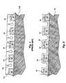
- FIG. 1is a cross-sectional view which depicts the undesirable result obtained by conventionally depositing an ozone-TEOS layer 11 over aluminum conductor lines 12 which overlie an underlying PECVD-TEOS glass layer 113 .
- the aluminum conductor lines 12Prior to patterning, the aluminum conductor lines 12 were covered with a titanium nitride layer which served as an anti-reflective coating during a laser reflow operation.
- a titanium nitride layer 14 remnantis present on the upper surface of each aluminum conductor line 12 .
- a cavity 15 having a teardrop-shaped cross sectionhas formed between each pair of aluminum conductor lines 12 .
- Cavities in an interlevel dielectric layerare problematic primarily because they can trap moisture when the deposited glass layer is subjected to a planarizing chemical mechanical polishing step during a subsequent fabrication step. The moisture, if not completely removed prior to the deposition of subsequent layers, can corrode metal conductor lines during normal use and operation of the part, or it may cause an encapsulated integrated circuit device to rupture if the steam generated as the device heats up is unable to escape the package.
- This inventionprovides an alternative method for depositing highly conformal silicate glass layers via chemical vapor deposition through the reaction of TEOS and O 3 and for minimizing surface effects of different materials on the deposition process.
- the entire methodbegins by placing an in-process integrated circuit having multiple surface constituents in a plasma-enhanced chemical vapor deposition chamber.
- a “clean” silicate glass base layer that is substantially free of carbon particle impurities on an upper surface thereofis then formed on the wafer surface in one of two ways.
- the first way of forming the clean base layeremploys plasma-enhanced chemical vapor deposition using TEOS and diatomic oxygen gases as precursors to first deposit a “dirty” silicate glass base layer having carbon particle impurities imbedded on the upper surface. Glass layers deposited via PECVD by the reaction of TEOS and O 2 tend to have elemental carbon particles embedded therein.
- the glass base layeris subjected to a plasma treatment which involves flowing a mixture of an oxygen-containing diamagnetic oxidant, such as ozone or hydrogen peroxide or a combination of both, and diatomic oxygen gas into the chamber and striking an RF plasma at a power of 50-350 watts for a period of from 30-300 seconds. It is hypothesized that the plasma treatment burns off the carbon particle impurities that are present on the surface of the dirty silicate glass base layer, thereby reducing the hydrophilic surface characteristics. The plasma treatment also creates a high degree of surface uniformity on the PECVD-deposited O 2 -TEOS glass layer.
- a plasma treatmentwhich involves flowing a mixture of an oxygen-containing diamagnetic oxidant, such as ozone or hydrogen peroxide or a combination of both, and diatomic oxygen gas into the chamber and striking an RF plasma at a power of 50-350 watts for a period of from 30-300 seconds. It is hypothesized that the plasma treatment burns off the carbon particle impurities that
- the second way of forming the base layerinvolves flowing hydrogen peroxide vapor and at least one gaseous compound selected from the group consisting of silane and disilane into the deposition chamber.
- the clean base layer formed via this second methodmay be subjected to a plasma treatment identical to that performed on the dirty PECVD-deposited O 2 -TEOS glass layer.
- This optional plasma treatment stepis performed merely to improve surface uniformity, not reduce hydrophilic surface characteristics.
- a final glass layeris deposited over the PECVD-deposited glass layer using chemical vapor deposition and TEOS and ozone as precursor compounds.
- FIG. 1is a cross-sectional view of a portion of an in-process integrated circuit which has been subjected to a conventional blanket deposition of ozone-TEOS silicate glass;
- FIG. 2is a cross-sectional view of a portion of an in-process integrated circuit identical to that of FIG. 1 following deposition of a glass base layer;
- FIG. 3is a cross-sectional view of the in-process circuit portion of FIG. 2 following plasma treatment
- FIG. 4is a cross-sectional view of the in-process circuit portion of FIG. 3 following the deposition of a final ozone-TEOS glass layer;
- FIG. 5is a flow chart summarizing the various steps of the invention.
- This inventionis embodied in a process for depositing highly conformal silicate glass layers via chemical vapor deposition through the reaction of tetraethylorthosilane (TEOS) and O 3 .
- the entire processwhich can be performed in a single cluster tool or even in a single chamber, begins by placing an in-process semiconductor wafer in a plasma-enhanced chemical vapor deposition chamber.
- hundreds of integrated circuitsare undergoing simultaneous fabrication on the wafer, and each integrated circuit has topography with multiple surface constituents.
- FIG. 2is a cross-sectional view which depicts a small portion of an integrated circuit identical to that of FIG. 1 .
- a plurality of parallel aluminum conductor lines 12overlies a silicon dioxide layer 13 (previously referred to as PECVD-TEOS layer 113 ).
- PECVD-TEOS layer 113silicon dioxide layer 13
- Each aluminum conductor line 12is covered with a titanium nitride layer 14 which served as an anti-reflective coating during a laser reflow operation which preceded masking and etching steps which formed the conductor lines.
- Each of the different materialshas different surface characteristics which affect the rate of deposition for ozone-TEOS glass layers.
- a “clean” silicate glass base layeris formed which completely covers all existing topography.
- the base layermust be clean in the sense that its upper surface is free of hydrophilic carbon particle impurities which would interfere with the deposition of an ozone-TEOS final glass layer.
- the clean base layermay be formed in one of two ways.
- the first wayinvolves depositing a “dirty” silicate glass base layer 21 on all constituent surfaces via plasma-enhanced chemical vapor deposition (PECVD).
- PECVD deposition of the silicate glass base layer 21is performed in a deposition chamber in which a plasma is formed from a mixture of TEOS, oxygen and an inert carrier gas such as helium or argon which transports TEOS molecules to the chamber.
- Deposition of the PECVD silicate glass base layer 21is effected within a plasma deposition chamber at a pressure within a range of about 1-50 torr (preferably within a range of about 1-10 torr), an oxygen flow rate of about 100-1000 sccm, a carrier gas flow rate of about 100-1500 sccm, and with an RF power density of about 0.7 watts/cm 2 to about 3.0 watt/cm 2 .
- the deposition temperatureis maintained within a range of about 300 to 500° C., with a preferred temperature of about 375° C. This process is described in greater detail in U.S. Pat. No. 4,872,947, which issued to Chang et al., and is assigned to Applied Materials, Inc. This patent is incorporated herein by reference.
- Silicate glass layerscan be deposited using standard high frequency RF power or a mixed frequency RF power.
- the silicate glass base layer 21is deposited to an average thickness within a range of about 100 to 1000 ⁇ .
- the optimum thicknessis deemed to be approximately 500 ⁇ .
- the deposition rate of plasma-enhanced chemical-vapor-deposited oxide from TEOS and O 2is more even on different surfaces than it is for ozone-TEOS oxide, it is essential that all surfaces are completely covered.
- An untreated TEOS silicate glass layer deposited via a plasma-enhanced CVD processtends to have embedded elemental carbon particles which are formed as the TEOS precursor gas is attacked by oxygen radicals generated by the plasma. These carbon particles apparently impart hydrophilic surface characteristics to an untreated silicate glass base layer 21 which are most likely responsible for the uneven deposition rates observed during subsequent depositions of dense, high-quality PECVD ozone-TEOS glass layers.
- the dirty silicate glass base layer 21is subjected to a plasma treatment which involves flowing a mixture of an oxygen-containing diamagnetic oxidant gas, such as ozone (O 3 ) or hydrogen peroxide (H 2 O 2 ) or a combination of both, and diatomic oxygen (O 2 ) gas into the chamber and striking an RF plasma.
- an oxygen-containing diamagnetic oxidant gassuch as ozone (O 3 ) or hydrogen peroxide (H 2 O 2 ) or a combination of both
- diatomic oxygen (O 2 ) gasa mixture of 4 to 15 percent O 3 or H 2 O 2 in O 2 is admitted to the chamber at a flow rate of about 2,400 standard cc/min.
- the plasmais sustained at a power density setting of 0.25 watt/cm 2 to about 3.0 watt/cm 2 for a period of from 30-360 seconds.
- FIG. 3depicts a plasma cloud 31 which completely engulfs the in-process integrated circuit portion of FIG. 2 , thereby exposing all surfaces of the silicate glass base layer 21 to the oxygen plasma. It is hypothesized that the plasma treatment burns off impurities, such as the carbon particles, which are present in the PECVD-deposited silicate glass base layer 21 , thereby reducing or eliminating the hydrophilic surface characteristics.
- the plasma treatmentcreates a high degree of surface uniformity on the PECVD-deposited silicate glass base layer 21 .
- FIG. 2which may also be used to represent the second method of forming a clean silicate glass base layer 21 involves a non-plasma-enhanced chemical vapor deposition effected by flowing hydrogen peroxide vapor and at least one gaseous compound selected from the group consisting of silane and disilane into the deposition chamber.
- a clean silicate glass base layer having no imbedded carbon particle impuritiesis deposited.
- the reaction of hydrogen peroxide vapor with either silane or disilaneis performed within a temperature range of about 0° C.
- the hydrogen peroxideis introduced into the deposition chamber in combination with at least one carrier gas selected from the group consisting of nitrogen and the noble gases.
- the hydrogen peroxideis picked up by the carrier gas in a bubbler apparatus, and the flow rate of the carrier gas (with the hydrogen peroxide) into the deposition chamber is maintained within a range of about 50 sccm to 1,000 sccm.
- the hydrogen peroxidemay be introduced into the deposition chamber via liquid injection using a liquid-flow controller in combination with a vaporizer.
- the clean base layer formed via this second methodmay be subjected to a plasma treatment identical to that performed on the dirty PECVD-deposited O 2 -TEOS glass layer.
- This optional plasma treatment stepis performed merely to improve surface uniformity, not reduce hydrophilic surface characteristics.
- an ozone-TEOS silicate glass layer 41is deposited on top of the clean silicate glass base layer 42 .
- the same chambercan be used for all process steps.
- the plasma treatment stepthe TEOS flow and the concomitant carrier gas flow are terminated, plasma generation continues, and ozone is added to the still flowing O 2 gas.
- the ozone-TEOS deposition stepthe TEOS flow is resumed and the O 2 and O 3 ratios are adjusted as necessary.
- the ozone-TEOS deposition stepis accomplished by flowing TEOS, oxygen and ozone gases into the deposition chamber, which is maintained at a pressure greater than 10 torr, and, preferably, within a range of about 500 to 760 torr. Substrate temperatures are maintained within a range of about 300-600° C., and preferably at a temperature of about 400° C.
- a dense, highly conformal ozone-TEOS silicate glass layer 41is deposited that rapidly fills in the remaining gaps between the aluminum conductor lines 12 .
- the ozone-TEOS silicate glass layer 41demonstrates a high degree of conformality upon deposition. Cavities present in ozone-TEOS silicate glass layers deposited using conventional deposition methods are eliminated.
- the present processis highly advantageous because deposition of the PECVD silicate glass base layer 21 , plasma treatment of the silicate glass base layer 21 , and deposition of the ozone-TEOS silicate glass layer 41 can be performed in sequence, in the same reaction chamber, requiring a minimum of changes in the reactor, and without having to remove the substrate from the reaction chamber between the various steps.
- the silicate glass base layeris deposited using hydrogen peroxide and silane or disilane as precursors, all steps may be performed within the same reaction chamber without having to remove the substrate from the chamber between the various steps.
- FIG. 5summarizes the various options of the process which is the subject of this disclosure.
- the first major stepproviding a “clean” silicate glass base layer 51 , can be performed in two basic ways: the dirty deposition and cleaning route 52 using TEOS and O 2 as precursor gases for a PECVD deposition step 53 followed by a cleaning plasma treatment step 54 involving O 2 and H 2 O 2 and/or O 3 , or the CVD route 55 using silane or disilane and H 2 O 2 as precursor gases in a CVD deposition step 56 and, optionally, the plasma surface treatment of step 54 .
- the final step 57is CVD deposition of a final glass layer using TEOS and O 3 as precursor gases.
Landscapes
- Engineering & Computer Science (AREA)
- Chemical & Material Sciences (AREA)
- Physics & Mathematics (AREA)
- Condensed Matter Physics & Semiconductors (AREA)
- General Physics & Mathematics (AREA)
- Manufacturing & Machinery (AREA)
- Computer Hardware Design (AREA)
- Microelectronics & Electronic Packaging (AREA)
- Power Engineering (AREA)
- Materials Engineering (AREA)
- Organic Chemistry (AREA)
- General Chemical & Material Sciences (AREA)
- Chemical Kinetics & Catalysis (AREA)
- Metallurgy (AREA)
- Mechanical Engineering (AREA)
- Plasma & Fusion (AREA)
- Inorganic Chemistry (AREA)
- Life Sciences & Earth Sciences (AREA)
- Geochemistry & Mineralogy (AREA)
- Formation Of Insulating Films (AREA)
- Internal Circuitry In Semiconductor Integrated Circuit Devices (AREA)
Abstract
Description
- This application is a continuation of application Ser. No. 10/371,674, filed Feb. 21, 2003, pending, which is a continuation of application Ser. No. 08/841,908, filed Apr. 17, 1997, now U.S. Pat. No. 6,551,665, issued Apr. 22, 2003.
- 1. Field of the Invention
- This invention relates to processes for depositing compounds by means of chemical vapor deposition and, more particularly, to processes for depositing silicon dioxide layers using ozone and tetraethylorthosilane as precursor compounds.
- 2. State of the Art
- Doped and undoped silicon dioxides, which are commonly referred to as silicate glasses, are widely used as dielectrics in integrated circuits. Although silicon dioxide possesses a tetrahedral matrix which will impart a crystalline structure to the material under proper heating and cooling conditions, the silicon dioxides used as dielectrics in integrated circuits are typically amorphous materials. This application uses the term “silicate glass” to refer to silicon dioxides deposited via chemical vapor deposition (CVD), as the term encompasses materials containing not just silicon dioxide, but dopants and other impurities as well.
- Chemical vapor deposition of silicate glasses has become of paramount importance in the manufacture of contemporary integrated circuits. For example, silicate glass doped with both boron and phosphorous is widely used as an interlevel dielectric and as a getter material for mobile sodium ions.
- Chemical vapor deposition (CVD) of silicate glasses by the semiconductor industry is most commonly accomplished by reacting tetraethylorthosilane (TEOS), silane or disilane with an oxidizer. Silane is typically reacted with diatomic oxygen (O2) or nitrous oxide (N2O) at a temperature of about 400° C. TEOS, on the other hand, is generally reacted with either O2or ozone (O3). If a low reaction temperature is desirable, the use of ozone permits a reduction in the reaction temperature to about half that required for O2. For the sake of brevity, glass layers deposited from the reaction of O3and TEOS shall be termed “ozone-TEOS glasses.” The reaction temperature may also be reduced for the TEOS-O2reaction by striking a plasma in the deposition chamber. Glasses deposited via this plasma-enhanced chemical vapor deposition (PECVD) method shall be referred to hereinafter as PECVD-TEOS silicate glasses. The plasma generates highly reactive oxygen radicals which can react with the TEOS molecules and provide rapid deposition rates at much reduced temperatures.
- Silane is used for the deposition of silicate glasses when substrate topography is minimal, as the deposited layers are characterized by poor conformality and poor step coverage. Silicate glasses deposited from the reaction of TEOS with O2or O3are being used with increasing frequency as interlevel dielectrics because the deposited layers demonstrate remarkable conformality that permits the filling of gaps as narrow as 0.25 μm. Unfortunately, the deposition rate of silicate glass formed by the reaction of TEOS and O3is highly surface dependent. A particularly acute problem arises when the deposition is performed on a surface having topographical features with non-uniform surface characteristics. For example, the deposition rate is very slow on PECVD-TEOS glass layers, considerably faster on silicon and on aluminum alloys, and faster still on titanium nitride, which is frequently used as an anti-reflective coating for laser reflow of aluminum alloy layers. A correlation seems to exist between the quality and relative deposition rate of ozone-TEOS glass layers. For example, ozone-TEOS glass layers that are deposited on PECVD-TEOS glass layers have rough, porous surfaces and possess high etch rates.
- In U.S. Pat. No. 5,271,972 to K. Kwok et al., it is suggested that the surface sensitivity of ozone-TEOS glass layers deposited on PECVD-TEOS glass layers may be related to the presence of a hydrophilic surface on the PECVD-TEOS glass layers. A hydrophilic surface on the PECVD-TEOS glass layer may be attributable to embedded elemental carbon particles which are formed as the TEOS precursor gas is attached by oxygen radicals generated by the plasma. As elemental carbon particles are characteristically hydrophilic, they repel TEOS molecules, which are characteristically hydrophobic, and interfere with their absorption on the surface of the deposited layer. Thus, the poor absorption rate of TEOS molecules on the surface of PECVD-TEOS glass results in slowly deposited, poor-quality films. Experimental evidence indicates that deposition rates are low for hydrophilic surfaces and high for hydrophobic surfaces. For example, titanium nitride, being highly hydrophobic, readily absorbs TEOS molecules on its surface, which accelerates the deposition reaction.
- Given the surface-dependent variation in deposition rates, it is not uncommon for ozone-TEOS glass layers to build up rapidly around aluminum conductor lines and much more slowly on PECVD glass layers on which the conductor lines are fabricated, thereby forming cavities of tear-drop cross section between adjacent conductor lines.
FIG. 1 is a cross-sectional view which depicts the undesirable result obtained by conventionally depositing an ozone-TEOS layer 11 overaluminum conductor lines 12 which overlie an underlying PECVD-TEOS glass layer 113. Prior to patterning, thealuminum conductor lines 12 were covered with a titanium nitride layer which served as an anti-reflective coating during a laser reflow operation. Atitanium nitride layer 14 remnant is present on the upper surface of eachaluminum conductor line 12. Acavity 15 having a teardrop-shaped cross section has formed between each pair ofaluminum conductor lines 12. Cavities in an interlevel dielectric layer are problematic primarily because they can trap moisture when the deposited glass layer is subjected to a planarizing chemical mechanical polishing step during a subsequent fabrication step. The moisture, if not completely removed prior to the deposition of subsequent layers, can corrode metal conductor lines during normal use and operation of the part, or it may cause an encapsulated integrated circuit device to rupture if the steam generated as the device heats up is unable to escape the package. - In U.S. Pat. No. 5,271,972, a technique is disclosed for improving the film quality of ozone-TEOS glass layers deposited on PECVD-TEOS glass layers. The method involves depositing the underlying PECVD-TEOS layer using high pressure and a high ozone-to-TEOS flow rate. For the last several seconds of the plasma-enhanced deposition process, a stepwise reduction in reactor power is carried out. It is claimed that this technique produces an interstitial silicon dioxide layer at the surface of the PECVD-TEOS layer which greatly reduces the surface sensitivity of subsequently deposited ozone-TEOS oxide layers.
- This invention provides an alternative method for depositing highly conformal silicate glass layers via chemical vapor deposition through the reaction of TEOS and O3and for minimizing surface effects of different materials on the deposition process.
- The entire method, which can be performed in a single cluster tool or even in a single chamber, begins by placing an in-process integrated circuit having multiple surface constituents in a plasma-enhanced chemical vapor deposition chamber. A “clean” silicate glass base layer that is substantially free of carbon particle impurities on an upper surface thereof is then formed on the wafer surface in one of two ways.
- The first way of forming the clean base layer employs plasma-enhanced chemical vapor deposition using TEOS and diatomic oxygen gases as precursors to first deposit a “dirty” silicate glass base layer having carbon particle impurities imbedded on the upper surface. Glass layers deposited via PECVD by the reaction of TEOS and O2tend to have elemental carbon particles embedded therein. As these particles may impart hydrophilic surface characteristics to the deposited glass layer which may interfere with the subsequent deposition of dense, high-quality ozone-TEOS glass layers, the glass base layer is subjected to a plasma treatment which involves flowing a mixture of an oxygen-containing diamagnetic oxidant, such as ozone or hydrogen peroxide or a combination of both, and diatomic oxygen gas into the chamber and striking an RF plasma at a power of 50-350 watts for a period of from 30-300 seconds. It is hypothesized that the plasma treatment burns off the carbon particle impurities that are present on the surface of the dirty silicate glass base layer, thereby reducing the hydrophilic surface characteristics. The plasma treatment also creates a high degree of surface uniformity on the PECVD-deposited O2-TEOS glass layer.
- The second way of forming the base layer involves flowing hydrogen peroxide vapor and at least one gaseous compound selected from the group consisting of silane and disilane into the deposition chamber. As an optional step, the clean base layer formed via this second method may be subjected to a plasma treatment identical to that performed on the dirty PECVD-deposited O2-TEOS glass layer. This optional plasma treatment step is performed merely to improve surface uniformity, not reduce hydrophilic surface characteristics.
- Following the formation of the clean base layer, a final glass layer is deposited over the PECVD-deposited glass layer using chemical vapor deposition and TEOS and ozone as precursor compounds.
FIG. 1 is a cross-sectional view of a portion of an in-process integrated circuit which has been subjected to a conventional blanket deposition of ozone-TEOS silicate glass;FIG. 2 is a cross-sectional view of a portion of an in-process integrated circuit identical to that ofFIG. 1 following deposition of a glass base layer;FIG. 3 is a cross-sectional view of the in-process circuit portion ofFIG. 2 following plasma treatment;FIG. 4 is a cross-sectional view of the in-process circuit portion ofFIG. 3 following the deposition of a final ozone-TEOS glass layer; andFIG. 5 is a flow chart summarizing the various steps of the invention.- This invention is embodied in a process for depositing highly conformal silicate glass layers via chemical vapor deposition through the reaction of tetraethylorthosilane (TEOS) and O3. The entire process, which can be performed in a single cluster tool or even in a single chamber, begins by placing an in-process semiconductor wafer in a plasma-enhanced chemical vapor deposition chamber. In a typical case, hundreds of integrated circuits are undergoing simultaneous fabrication on the wafer, and each integrated circuit has topography with multiple surface constituents.
FIG. 2 is a cross-sectional view which depicts a small portion of an integrated circuit identical to that ofFIG. 1 . A plurality of parallel aluminum conductor lines12 overlies a silicon dioxide layer13 (previously referred to as PECVD-TEOS layer113). Eachaluminum conductor line 12 is covered with atitanium nitride layer 14 which served as an anti-reflective coating during a laser reflow operation which preceded masking and etching steps which formed the conductor lines. Each of the different materials has different surface characteristics which affect the rate of deposition for ozone-TEOS glass layers. - In order to eliminate surface characteristics, a “clean” silicate glass base layer is formed which completely covers all existing topography. The base layer must be clean in the sense that its upper surface is free of hydrophilic carbon particle impurities which would interfere with the deposition of an ozone-TEOS final glass layer. The clean base layer may be formed in one of two ways.
- Referring now to
FIG. 2 , the first way involves depositing a “dirty” silicateglass base layer 21 on all constituent surfaces via plasma-enhanced chemical vapor deposition (PECVD). The PECVD deposition of the silicateglass base layer 21 is performed in a deposition chamber in which a plasma is formed from a mixture of TEOS, oxygen and an inert carrier gas such as helium or argon which transports TEOS molecules to the chamber. - Deposition of the PECVD silicate
glass base layer 21 is effected within a plasma deposition chamber at a pressure within a range of about 1-50 torr (preferably within a range of about 1-10 torr), an oxygen flow rate of about 100-1000 sccm, a carrier gas flow rate of about 100-1500 sccm, and with an RF power density of about 0.7 watts/cm2to about 3.0 watt/cm2. The deposition temperature is maintained within a range of about 300 to 500° C., with a preferred temperature of about 375° C. This process is described in greater detail in U.S. Pat. No. 4,872,947, which issued to Chang et al., and is assigned to Applied Materials, Inc. This patent is incorporated herein by reference. - A suitable CVD/PECVD reactor in which the present process can be carried out in its entirety is also described in U.S. Pat. No. 4,872,947. Silicate glass layers can be deposited using standard high frequency RF power or a mixed frequency RF power.
- The silicate
glass base layer 21 is deposited to an average thickness within a range of about 100 to 1000 Å. The optimum thickness is deemed to be approximately 500 Å. Although the deposition rate of plasma-enhanced chemical-vapor-deposited oxide from TEOS and O2is more even on different surfaces than it is for ozone-TEOS oxide, it is essential that all surfaces are completely covered. - An untreated TEOS silicate glass layer deposited via a plasma-enhanced CVD process tends to have embedded elemental carbon particles which are formed as the TEOS precursor gas is attacked by oxygen radicals generated by the plasma. These carbon particles apparently impart hydrophilic surface characteristics to an untreated silicate
glass base layer 21 which are most likely responsible for the uneven deposition rates observed during subsequent depositions of dense, high-quality PECVD ozone-TEOS glass layers. In order to reduce or eliminate such interfering surface characteristics, the dirty silicateglass base layer 21 is subjected to a plasma treatment which involves flowing a mixture of an oxygen-containing diamagnetic oxidant gas, such as ozone (O3) or hydrogen peroxide (H2O2) or a combination of both, and diatomic oxygen (O2) gas into the chamber and striking an RF plasma. A mixture of 4 to 15 percent O3or H2O2in O2is admitted to the chamber at a flow rate of about 2,400 standard cc/min. The plasma is sustained at a power density setting of 0.25 watt/cm2to about 3.0 watt/cm2for a period of from 30-360 seconds. In order to prevent etching of the deposited silicateglass base layer 21 and uncovering of additional impurity sites, a remote-source plasma generator is preferred over a parallel-plate reactor. The plasma treatment is represented byFIG. 3 , which depicts aplasma cloud 31 which completely engulfs the in-process integrated circuit portion ofFIG. 2 , thereby exposing all surfaces of the silicateglass base layer 21 to the oxygen plasma. It is hypothesized that the plasma treatment burns off impurities, such as the carbon particles, which are present in the PECVD-deposited silicateglass base layer 21, thereby reducing or eliminating the hydrophilic surface characteristics. The plasma treatment creates a high degree of surface uniformity on the PECVD-deposited silicateglass base layer 21. - Referring once again to
FIG. 2 , which may also be used to represent the second method of forming a clean silicateglass base layer 21 involves a non-plasma-enhanced chemical vapor deposition effected by flowing hydrogen peroxide vapor and at least one gaseous compound selected from the group consisting of silane and disilane into the deposition chamber. A clean silicate glass base layer having no imbedded carbon particle impurities is deposited. The reaction of hydrogen peroxide vapor with either silane or disilane is performed within a temperature range of about 0° C. to 40° C., at a chamber pressure of less than about 10 torr, and at a flow rate maintained for silane or disilane within a range of about 10 sccm to 1,000 sccm. The hydrogen peroxide is introduced into the deposition chamber in combination with at least one carrier gas selected from the group consisting of nitrogen and the noble gases. The hydrogen peroxide is picked up by the carrier gas in a bubbler apparatus, and the flow rate of the carrier gas (with the hydrogen peroxide) into the deposition chamber is maintained within a range of about 50 sccm to 1,000 sccm. In addition, the hydrogen peroxide may be introduced into the deposition chamber via liquid injection using a liquid-flow controller in combination with a vaporizer. - As an optional step, the clean base layer formed via this second method may be subjected to a plasma treatment identical to that performed on the dirty PECVD-deposited O2-TEOS glass layer. This optional plasma treatment step is performed merely to improve surface uniformity, not reduce hydrophilic surface characteristics.
- Referring now to
FIG. 4 , an ozone-TEOSsilicate glass layer 41 is deposited on top of the clean silicateglass base layer 42. As the processes required for the formation of the silicate glass base layer, the plasma treatment step, and the ozone-TEOS deposition step share certain parameters in common, the same chamber can be used for all process steps. For the plasma treatment step, the TEOS flow and the concomitant carrier gas flow are terminated, plasma generation continues, and ozone is added to the still flowing O2gas. For the ozone-TEOS deposition step, the TEOS flow is resumed and the O2and O3ratios are adjusted as necessary. The ozone-TEOS deposition step is accomplished by flowing TEOS, oxygen and ozone gases into the deposition chamber, which is maintained at a pressure greater than 10 torr, and, preferably, within a range of about 500 to 760 torr. Substrate temperatures are maintained within a range of about 300-600° C., and preferably at a temperature of about 400° C. A dense, highly conformal ozone-TEOSsilicate glass layer 41 is deposited that rapidly fills in the remaining gaps between the aluminum conductor lines12. The ozone-TEOSsilicate glass layer 41 demonstrates a high degree of conformality upon deposition. Cavities present in ozone-TEOS silicate glass layers deposited using conventional deposition methods are eliminated. - The present process is highly advantageous because deposition of the PECVD silicate
glass base layer 21, plasma treatment of the silicateglass base layer 21, and deposition of the ozone-TEOSsilicate glass layer 41 can be performed in sequence, in the same reaction chamber, requiring a minimum of changes in the reactor, and without having to remove the substrate from the reaction chamber between the various steps. Likewise, if the silicate glass base layer is deposited using hydrogen peroxide and silane or disilane as precursors, all steps may be performed within the same reaction chamber without having to remove the substrate from the chamber between the various steps. FIG. 5 summarizes the various options of the process which is the subject of this disclosure. The first major step, providing a “clean” silicateglass base layer 51, can be performed in two basic ways: the dirty deposition and cleaningroute 52 using TEOS and O2as precursor gases for aPECVD deposition step 53 followed by a cleaningplasma treatment step 54 involving O2and H2O2and/or O3, or theCVD route 55 using silane or disilane and H2O2as precursor gases in aCVD deposition step 56 and, optionally, the plasma surface treatment ofstep 54. Thefinal step 57 is CVD deposition of a final glass layer using TEOS and O3as precursor gases.- Various changes to the gas mixtures, temperature and pressure of the reactions are contemplated and are meant to be included herein. Although the ozone-TEOS glass deposition process is described in terms of only a single embodiment, it will be obvious to those having ordinary skill in the art of semiconductor integrated circuit fabrication that changes and modifications may be made thereto without departing from the scope and the spirit of the invention as hereinafter claimed.
Claims (98)
Priority Applications (2)
| Application Number | Priority Date | Filing Date | Title |
|---|---|---|---|
| US10/928,505US7101815B2 (en) | 1997-04-17 | 2004-08-26 | Method for improving thickness uniformity of deposited ozone-TEOS silicate glass layers |
| US11/175,869US20050255689A1 (en) | 1997-04-17 | 2005-07-06 | Method for improving thickness uniformity of deposited ozone-TEOS silicate glass layers |
Applications Claiming Priority (3)
| Application Number | Priority Date | Filing Date | Title |
|---|---|---|---|
| US08/841,908US6551665B1 (en) | 1997-04-17 | 1997-04-17 | Method for improving thickness uniformity of deposited ozone-TEOS silicate glass layers |
| US10/371,674US6784122B2 (en) | 1997-04-17 | 2003-02-21 | Method for improving thickness uniformity of deposited ozone-TEOS silicate glass layers |
| US10/928,505US7101815B2 (en) | 1997-04-17 | 2004-08-26 | Method for improving thickness uniformity of deposited ozone-TEOS silicate glass layers |
Related Parent Applications (1)
| Application Number | Title | Priority Date | Filing Date |
|---|---|---|---|
| US10/371,674ContinuationUS6784122B2 (en) | 1997-04-17 | 2003-02-21 | Method for improving thickness uniformity of deposited ozone-TEOS silicate glass layers |
Related Child Applications (1)
| Application Number | Title | Priority Date | Filing Date |
|---|---|---|---|
| US11/175,869DivisionUS20050255689A1 (en) | 1997-04-17 | 2005-07-06 | Method for improving thickness uniformity of deposited ozone-TEOS silicate glass layers |
Publications (2)
| Publication Number | Publication Date |
|---|---|
| US20050032394A1true US20050032394A1 (en) | 2005-02-10 |
| US7101815B2 US7101815B2 (en) | 2006-09-05 |
Family
ID=25286011
Family Applications (10)
| Application Number | Title | Priority Date | Filing Date |
|---|---|---|---|
| US08/841,908Expired - LifetimeUS6551665B1 (en) | 1997-04-17 | 1997-04-17 | Method for improving thickness uniformity of deposited ozone-TEOS silicate glass layers |
| US09/222,565Expired - LifetimeUS6107214A (en) | 1997-04-17 | 1998-12-29 | Method for improving thickness uniformity of deposited ozone-TEOS silicate glass layers |
| US09/548,572Expired - LifetimeUS6251807B1 (en) | 1997-04-17 | 2000-04-13 | Method for improving thickness uniformity of deposited ozone-teos silicate glass layers |
| US09/548,491Expired - Fee RelatedUS6297175B1 (en) | 1997-04-17 | 2000-04-13 | Method for improving thickness uniformity of deposited ozone-TEOS silicate glass layers |
| US09/935,833Expired - Fee RelatedUS6458721B2 (en) | 1997-04-17 | 2001-08-23 | Method for improving thickness uniformity of deposited ozone-TEOS silicate glass layers |
| US10/200,845Expired - LifetimeUS6576570B2 (en) | 1997-04-17 | 2002-07-22 | Method for improving thickness uniformity of deposited ozone-teos silicate glass layers |
| US10/371,674Expired - Fee RelatedUS6784122B2 (en) | 1997-04-17 | 2003-02-21 | Method for improving thickness uniformity of deposited ozone-TEOS silicate glass layers |
| US10/457,298Expired - Fee RelatedUS6815374B2 (en) | 1997-04-17 | 2003-06-09 | Method for improving thickness uniformity of deposited ozone-TEOS silicate glass layers |
| US10/928,505Expired - Fee RelatedUS7101815B2 (en) | 1997-04-17 | 2004-08-26 | Method for improving thickness uniformity of deposited ozone-TEOS silicate glass layers |
| US11/175,869AbandonedUS20050255689A1 (en) | 1997-04-17 | 2005-07-06 | Method for improving thickness uniformity of deposited ozone-TEOS silicate glass layers |
Family Applications Before (8)
| Application Number | Title | Priority Date | Filing Date |
|---|---|---|---|
| US08/841,908Expired - LifetimeUS6551665B1 (en) | 1997-04-17 | 1997-04-17 | Method for improving thickness uniformity of deposited ozone-TEOS silicate glass layers |
| US09/222,565Expired - LifetimeUS6107214A (en) | 1997-04-17 | 1998-12-29 | Method for improving thickness uniformity of deposited ozone-TEOS silicate glass layers |
| US09/548,572Expired - LifetimeUS6251807B1 (en) | 1997-04-17 | 2000-04-13 | Method for improving thickness uniformity of deposited ozone-teos silicate glass layers |
| US09/548,491Expired - Fee RelatedUS6297175B1 (en) | 1997-04-17 | 2000-04-13 | Method for improving thickness uniformity of deposited ozone-TEOS silicate glass layers |
| US09/935,833Expired - Fee RelatedUS6458721B2 (en) | 1997-04-17 | 2001-08-23 | Method for improving thickness uniformity of deposited ozone-TEOS silicate glass layers |
| US10/200,845Expired - LifetimeUS6576570B2 (en) | 1997-04-17 | 2002-07-22 | Method for improving thickness uniformity of deposited ozone-teos silicate glass layers |
| US10/371,674Expired - Fee RelatedUS6784122B2 (en) | 1997-04-17 | 2003-02-21 | Method for improving thickness uniformity of deposited ozone-TEOS silicate glass layers |
| US10/457,298Expired - Fee RelatedUS6815374B2 (en) | 1997-04-17 | 2003-06-09 | Method for improving thickness uniformity of deposited ozone-TEOS silicate glass layers |
Family Applications After (1)
| Application Number | Title | Priority Date | Filing Date |
|---|---|---|---|
| US11/175,869AbandonedUS20050255689A1 (en) | 1997-04-17 | 2005-07-06 | Method for improving thickness uniformity of deposited ozone-TEOS silicate glass layers |
Country Status (1)
| Country | Link |
|---|---|
| US (10) | US6551665B1 (en) |
Cited By (2)
| Publication number | Priority date | Publication date | Assignee | Title |
|---|---|---|---|---|
| US20090011607A1 (en)* | 2007-07-05 | 2009-01-08 | John Smythe | Silicon Dioxide Deposition Methods Using at Least Ozone and TEOS as Deposition Precursors |
| US20110092077A1 (en)* | 2006-03-31 | 2011-04-21 | Huiwen Xu | Method to minimize wet etch undercuts and provide pore sealing of extreme low k (k<2.5) dielectrics |
Families Citing this family (54)
| Publication number | Priority date | Publication date | Assignee | Title |
|---|---|---|---|---|
| US6551665B1 (en) | 1997-04-17 | 2003-04-22 | Micron Technology, Inc. | Method for improving thickness uniformity of deposited ozone-TEOS silicate glass layers |
| US6303523B2 (en)* | 1998-02-11 | 2001-10-16 | Applied Materials, Inc. | Plasma processes for depositing low dielectric constant films |
| US6384466B1 (en)* | 1998-08-27 | 2002-05-07 | Micron Technology, Inc. | Multi-layer dielectric and method of forming same |
| JP3184177B2 (en)* | 1999-03-26 | 2001-07-09 | キヤノン販売株式会社 | Method for forming interlayer insulating film, semiconductor manufacturing apparatus, and semiconductor device |
| US6511924B2 (en) | 2001-04-20 | 2003-01-28 | Applied Materials, Inc. | Method of forming a silicon oxide layer on a substrate |
| US7067439B2 (en) | 2002-06-14 | 2006-06-27 | Applied Materials, Inc. | ALD metal oxide deposition process using direct oxidation |
| US6939817B2 (en)* | 2003-05-08 | 2005-09-06 | Micron Technology, Inc. | Removal of carbon from an insulative layer using ozone |
| US7485162B2 (en) | 2003-09-30 | 2009-02-03 | Fujimi Incorporated | Polishing composition |
| JP4049119B2 (en)* | 2004-03-26 | 2008-02-20 | セイコーエプソン株式会社 | Method for manufacturing ferroelectric memory device |
| DE602004017518D1 (en)* | 2004-04-06 | 2008-12-11 | Lg Electronics Inc | METAL PRODUCT COATED WITH ULTRAHYDROPHILIC AND ANTIBACTERIAL THIN FILM AND METHOD OF MANUFACTURING THEREOF |
| US8119210B2 (en) | 2004-05-21 | 2012-02-21 | Applied Materials, Inc. | Formation of a silicon oxynitride layer on a high-k dielectric material |
| KR100624566B1 (en)* | 2004-05-31 | 2006-09-19 | 주식회사 하이닉스반도체 | Semiconductor device having a fluid insulating film on top of capacitor and its manufacturing method |
| US20060105114A1 (en)* | 2004-11-16 | 2006-05-18 | White John M | Multi-layer high quality gate dielectric for low-temperature poly-silicon TFTs |
| US7371695B2 (en)* | 2006-01-04 | 2008-05-13 | Promos Technologies Pte. Ltd. | Use of TEOS oxides in integrated circuit fabrication processes |
| US7837838B2 (en) | 2006-03-09 | 2010-11-23 | Applied Materials, Inc. | Method of fabricating a high dielectric constant transistor gate using a low energy plasma apparatus |
| US7645710B2 (en) | 2006-03-09 | 2010-01-12 | Applied Materials, Inc. | Method and apparatus for fabricating a high dielectric constant transistor gate using a low energy plasma system |
| US7678710B2 (en) | 2006-03-09 | 2010-03-16 | Applied Materials, Inc. | Method and apparatus for fabricating a high dielectric constant transistor gate using a low energy plasma system |
| US8232176B2 (en) | 2006-06-22 | 2012-07-31 | Applied Materials, Inc. | Dielectric deposition and etch back processes for bottom up gapfill |
| US7718553B2 (en)* | 2006-09-21 | 2010-05-18 | Asm Japan K.K. | Method for forming insulation film having high density |
| US7902018B2 (en) | 2006-09-26 | 2011-03-08 | Applied Materials, Inc. | Fluorine plasma treatment of high-k gate stack for defect passivation |
| US7781352B2 (en)* | 2007-06-06 | 2010-08-24 | Asm Japan K.K. | Method for forming inorganic silazane-based dielectric film |
| US7914856B2 (en)* | 2007-06-29 | 2011-03-29 | General Electric Company | Method of preparing wetting-resistant surfaces and articles incorporating the same |
| US7867923B2 (en) | 2007-10-22 | 2011-01-11 | Applied Materials, Inc. | High quality silicon oxide films by remote plasma CVD from disilane precursors |
| US7651959B2 (en) | 2007-12-03 | 2010-01-26 | Asm Japan K.K. | Method for forming silazane-based dielectric film |
| US8357435B2 (en)* | 2008-05-09 | 2013-01-22 | Applied Materials, Inc. | Flowable dielectric equipment and processes |
| US7622369B1 (en) | 2008-05-30 | 2009-11-24 | Asm Japan K.K. | Device isolation technology on semiconductor substrate |
| US20090325391A1 (en)* | 2008-06-30 | 2009-12-31 | Asm International Nv | Ozone and teos process for silicon oxide deposition |
| US20100080929A1 (en)* | 2008-09-30 | 2010-04-01 | General Electric Company | System and method for applying a conformal barrier coating |
| US8765233B2 (en)* | 2008-12-09 | 2014-07-01 | Asm Japan K.K. | Method for forming low-carbon CVD film for filling trenches |
| US8511281B2 (en)* | 2009-07-10 | 2013-08-20 | Tula Technology, Inc. | Skip fire engine control |
| US8980382B2 (en) | 2009-12-02 | 2015-03-17 | Applied Materials, Inc. | Oxygen-doping for non-carbon radical-component CVD films |
| US8741788B2 (en) | 2009-08-06 | 2014-06-03 | Applied Materials, Inc. | Formation of silicon oxide using non-carbon flowable CVD processes |
| US8449942B2 (en) | 2009-11-12 | 2013-05-28 | Applied Materials, Inc. | Methods of curing non-carbon flowable CVD films |
| JP2013516763A (en) | 2009-12-30 | 2013-05-13 | アプライド マテリアルズ インコーポレイテッド | Dielectric film growth using radicals generated using a flexible nitrogen / hydrogen ratio |
| US8329262B2 (en) | 2010-01-05 | 2012-12-11 | Applied Materials, Inc. | Dielectric film formation using inert gas excitation |
| SG182336A1 (en) | 2010-01-06 | 2012-08-30 | Applied Materials Inc | Flowable dielectric using oxide liner |
| KR101837648B1 (en) | 2010-01-07 | 2018-04-19 | 어플라이드 머티어리얼스, 인코포레이티드 | Insitu ozone cure for radicalcomponent cvd |
| JP2013521650A (en) | 2010-03-05 | 2013-06-10 | アプライド マテリアルズ インコーポレイテッド | Conformal layer by radical component CVD |
| JP5052638B2 (en)* | 2010-03-17 | 2012-10-17 | Sppテクノロジーズ株式会社 | Deposition method |
| US9285168B2 (en) | 2010-10-05 | 2016-03-15 | Applied Materials, Inc. | Module for ozone cure and post-cure moisture treatment |
| US8664127B2 (en) | 2010-10-15 | 2014-03-04 | Applied Materials, Inc. | Two silicon-containing precursors for gapfill enhancing dielectric liner |
| US10283321B2 (en) | 2011-01-18 | 2019-05-07 | Applied Materials, Inc. | Semiconductor processing system and methods using capacitively coupled plasma |
| US8450191B2 (en) | 2011-01-24 | 2013-05-28 | Applied Materials, Inc. | Polysilicon films by HDP-CVD |
| US8716154B2 (en) | 2011-03-04 | 2014-05-06 | Applied Materials, Inc. | Reduced pattern loading using silicon oxide multi-layers |
| US8445078B2 (en) | 2011-04-20 | 2013-05-21 | Applied Materials, Inc. | Low temperature silicon oxide conversion |
| US8466073B2 (en) | 2011-06-03 | 2013-06-18 | Applied Materials, Inc. | Capping layer for reduced outgassing |
| US9404178B2 (en) | 2011-07-15 | 2016-08-02 | Applied Materials, Inc. | Surface treatment and deposition for reduced outgassing |
| US8617989B2 (en) | 2011-09-26 | 2013-12-31 | Applied Materials, Inc. | Liner property improvement |
| US20130252440A1 (en)* | 2011-09-26 | 2013-09-26 | Applied Materials, Inc. | Pretreatment and improved dielectric coverage |
| US8551891B2 (en) | 2011-10-04 | 2013-10-08 | Applied Materials, Inc. | Remote plasma burn-in |
| US8889566B2 (en) | 2012-09-11 | 2014-11-18 | Applied Materials, Inc. | Low cost flowable dielectric films |
| US9018108B2 (en) | 2013-01-25 | 2015-04-28 | Applied Materials, Inc. | Low shrinkage dielectric films |
| CN105244269B (en)* | 2014-07-09 | 2018-10-23 | 中芯国际集成电路制造(上海)有限公司 | A kind of semiconductor devices and its manufacturing method |
| US9412581B2 (en) | 2014-07-16 | 2016-08-09 | Applied Materials, Inc. | Low-K dielectric gapfill by flowable deposition |
Citations (12)
| Publication number | Priority date | Publication date | Assignee | Title |
|---|---|---|---|---|
| US4872947A (en)* | 1986-12-19 | 1989-10-10 | Applied Materials, Inc. | CVD of silicon oxide using TEOS decomposition and in-situ planarization process |
| US4992306A (en)* | 1990-02-01 | 1991-02-12 | Air Products Abd Chemicals, Inc. | Deposition of silicon dioxide and silicon oxynitride films using azidosilane sources |
| US5271972A (en)* | 1992-08-17 | 1993-12-21 | Applied Materials, Inc. | Method for depositing ozone/TEOS silicon oxide films of reduced surface sensitivity |
| US5356722A (en)* | 1992-06-10 | 1994-10-18 | Applied Materials, Inc. | Method for depositing ozone/TEOS silicon oxide films of reduced surface sensitivity |
| US5362526A (en)* | 1986-12-19 | 1994-11-08 | Applied Materials, Inc. | Plasma-enhanced CVD process using TEOS for depositing silicon oxide |
| US5503882A (en)* | 1994-04-18 | 1996-04-02 | Advanced Micro Devices, Inc. | Method for planarizing an integrated circuit topography |
| US5593741A (en)* | 1992-11-30 | 1997-01-14 | Nec Corporation | Method and apparatus for forming silicon oxide film by chemical vapor deposition |
| US5626924A (en)* | 1994-09-08 | 1997-05-06 | Sony Corporation | Method of forming oxide film |
| US5776254A (en)* | 1994-12-28 | 1998-07-07 | Mitsubishi Denki Kabushiki Kaisha | Apparatus for forming thin film by chemical vapor deposition |
| US5827785A (en)* | 1996-10-24 | 1998-10-27 | Applied Materials, Inc. | Method for improving film stability of fluorosilicate glass films |
| US6107214A (en)* | 1997-04-17 | 2000-08-22 | Micron Technology, Inc. | Method for improving thickness uniformity of deposited ozone-TEOS silicate glass layers |
| US6514876B1 (en)* | 1999-09-07 | 2003-02-04 | Steag Rtp Systems, Inc. | Pre-metal dielectric rapid thermal processing for sub-micron technology |
Family Cites Families (3)
| Publication number | Priority date | Publication date | Assignee | Title |
|---|---|---|---|---|
| US5531834A (en)* | 1993-07-13 | 1996-07-02 | Tokyo Electron Kabushiki Kaisha | Plasma film forming method and apparatus and plasma processing apparatus |
| JP3963961B2 (en)* | 1994-08-31 | 2007-08-22 | 株式会社半導体エネルギー研究所 | Method for manufacturing semiconductor device |
| JPH08203890A (en)* | 1995-01-25 | 1996-08-09 | Sony Corp | Formation of interlayer insulation film in semiconductor device |
- 1997
- 1997-04-17USUS08/841,908patent/US6551665B1/ennot_activeExpired - Lifetime
- 1998
- 1998-12-29USUS09/222,565patent/US6107214A/ennot_activeExpired - Lifetime
- 2000
- 2000-04-13USUS09/548,572patent/US6251807B1/ennot_activeExpired - Lifetime
- 2000-04-13USUS09/548,491patent/US6297175B1/ennot_activeExpired - Fee Related
- 2001
- 2001-08-23USUS09/935,833patent/US6458721B2/ennot_activeExpired - Fee Related
- 2002
- 2002-07-22USUS10/200,845patent/US6576570B2/ennot_activeExpired - Lifetime
- 2003
- 2003-02-21USUS10/371,674patent/US6784122B2/ennot_activeExpired - Fee Related
- 2003-06-09USUS10/457,298patent/US6815374B2/ennot_activeExpired - Fee Related
- 2004
- 2004-08-26USUS10/928,505patent/US7101815B2/ennot_activeExpired - Fee Related
- 2005
- 2005-07-06USUS11/175,869patent/US20050255689A1/ennot_activeAbandoned
Patent Citations (19)
| Publication number | Priority date | Publication date | Assignee | Title |
|---|---|---|---|---|
| US4872947A (en)* | 1986-12-19 | 1989-10-10 | Applied Materials, Inc. | CVD of silicon oxide using TEOS decomposition and in-situ planarization process |
| US5362526A (en)* | 1986-12-19 | 1994-11-08 | Applied Materials, Inc. | Plasma-enhanced CVD process using TEOS for depositing silicon oxide |
| US4992306A (en)* | 1990-02-01 | 1991-02-12 | Air Products Abd Chemicals, Inc. | Deposition of silicon dioxide and silicon oxynitride films using azidosilane sources |
| US5356722A (en)* | 1992-06-10 | 1994-10-18 | Applied Materials, Inc. | Method for depositing ozone/TEOS silicon oxide films of reduced surface sensitivity |
| US5271972A (en)* | 1992-08-17 | 1993-12-21 | Applied Materials, Inc. | Method for depositing ozone/TEOS silicon oxide films of reduced surface sensitivity |
| US5593741A (en)* | 1992-11-30 | 1997-01-14 | Nec Corporation | Method and apparatus for forming silicon oxide film by chemical vapor deposition |
| US5503882A (en)* | 1994-04-18 | 1996-04-02 | Advanced Micro Devices, Inc. | Method for planarizing an integrated circuit topography |
| US5626924A (en)* | 1994-09-08 | 1997-05-06 | Sony Corporation | Method of forming oxide film |
| US5776254A (en)* | 1994-12-28 | 1998-07-07 | Mitsubishi Denki Kabushiki Kaisha | Apparatus for forming thin film by chemical vapor deposition |
| US5827785A (en)* | 1996-10-24 | 1998-10-27 | Applied Materials, Inc. | Method for improving film stability of fluorosilicate glass films |
| US6107214A (en)* | 1997-04-17 | 2000-08-22 | Micron Technology, Inc. | Method for improving thickness uniformity of deposited ozone-TEOS silicate glass layers |
| US6251807B1 (en)* | 1997-04-17 | 2001-06-26 | Micron Technology, Inc. | Method for improving thickness uniformity of deposited ozone-teos silicate glass layers |
| US6297175B1 (en)* | 1997-04-17 | 2001-10-02 | Micron Technology Inc. | Method for improving thickness uniformity of deposited ozone-TEOS silicate glass layers |
| US6458721B2 (en)* | 1997-04-17 | 2002-10-01 | Micron Technology, Inc. | Method for improving thickness uniformity of deposited ozone-TEOS silicate glass layers |
| US6551665B1 (en)* | 1997-04-17 | 2003-04-22 | Micron Technology, Inc. | Method for improving thickness uniformity of deposited ozone-TEOS silicate glass layers |
| US6576570B2 (en)* | 1997-04-17 | 2003-06-10 | Micron Technology, Inc. | Method for improving thickness uniformity of deposited ozone-teos silicate glass layers |
| US6784122B2 (en)* | 1997-04-17 | 2004-08-31 | Micron Technology, Inc. | Method for improving thickness uniformity of deposited ozone-TEOS silicate glass layers |
| US6815374B2 (en)* | 1997-04-17 | 2004-11-09 | Micron Technology, Inc. | Method for improving thickness uniformity of deposited ozone-TEOS silicate glass layers |
| US6514876B1 (en)* | 1999-09-07 | 2003-02-04 | Steag Rtp Systems, Inc. | Pre-metal dielectric rapid thermal processing for sub-micron technology |
Cited By (6)
| Publication number | Priority date | Publication date | Assignee | Title |
|---|---|---|---|---|
| US20110092077A1 (en)* | 2006-03-31 | 2011-04-21 | Huiwen Xu | Method to minimize wet etch undercuts and provide pore sealing of extreme low k (k<2.5) dielectrics |
| US20090011607A1 (en)* | 2007-07-05 | 2009-01-08 | John Smythe | Silicon Dioxide Deposition Methods Using at Least Ozone and TEOS as Deposition Precursors |
| US20100267246A1 (en)* | 2007-07-05 | 2010-10-21 | Micron Technology, Inc. | Silicon Dioxide Deposition Methods Using at Least Ozone and TEOS as Deposition Precursors |
| US7902084B2 (en)* | 2007-07-05 | 2011-03-08 | Micron Technology, Inc. | Silicon dioxide deposition methods using at least ozone and TEOS as deposition precursors |
| US8043975B2 (en) | 2007-07-05 | 2011-10-25 | Micron Technology, Inc. | Silicon dioxide deposition methods using at least ozone and TEOS as deposition precursors |
| US8304353B2 (en) | 2007-07-05 | 2012-11-06 | Micron Technology, Inc. | Silicon dioxide deposition methods using at least ozone and TEOS as deposition precursors |
Also Published As
| Publication number | Publication date |
|---|---|
| US6297175B1 (en) | 2001-10-02 |
| US6551665B1 (en) | 2003-04-22 |
| US6576570B2 (en) | 2003-06-10 |
| US20050255689A1 (en) | 2005-11-17 |
| US20010055889A1 (en) | 2001-12-27 |
| US20030203654A1 (en) | 2003-10-30 |
| US6815374B2 (en) | 2004-11-09 |
| US7101815B2 (en) | 2006-09-05 |
| US20030129852A1 (en) | 2003-07-10 |
| US6251807B1 (en) | 2001-06-26 |
| US6458721B2 (en) | 2002-10-01 |
| US6784122B2 (en) | 2004-08-31 |
| US6107214A (en) | 2000-08-22 |
| US20020182825A1 (en) | 2002-12-05 |
Similar Documents
| Publication | Publication Date | Title |
|---|---|---|
| US6784122B2 (en) | Method for improving thickness uniformity of deposited ozone-TEOS silicate glass layers | |
| TWI842531B (en) | Method of topology-selective film formation of silicon oxide | |
| US5356722A (en) | Method for depositing ozone/TEOS silicon oxide films of reduced surface sensitivity | |
| US5271972A (en) | Method for depositing ozone/TEOS silicon oxide films of reduced surface sensitivity | |
| US5869149A (en) | Method for preparing nitrogen surface treated fluorine doped silicon dioxide films | |
| US6787483B1 (en) | Gap fill for high aspect ratio structures | |
| US6110836A (en) | Reactive plasma etch cleaning of high aspect ratio openings | |
| US6905543B1 (en) | Methods of forming tungsten nucleation layer | |
| EP0572704B1 (en) | Method for manufacturing a semiconductor device including method of reforming an insulating film formed by low temperature CVD | |
| US4681653A (en) | Planarized dielectric deposited using plasma enhanced chemical vapor deposition | |
| US20110104400A1 (en) | Method for depositing an amorphous carbon film with improved density and step coverage | |
| US20080153311A1 (en) | Method for depositing an amorphous carbon film with improved density and step coverage | |
| US7001854B1 (en) | Hydrogen-based phosphosilicate glass process for gap fill of high aspect ratio structures | |
| EP0421203B1 (en) | An integrated circuit structure with a boron phosphorus silicate glass composite layer on semiconductor wafer and improved method for forming same | |
| US5382550A (en) | Method of depositing SiO2 on a semiconductor substrate | |
| US5281557A (en) | Soluble oxides for integrated circuit fabrication formed by the incomplete dissociation of the precursor gas | |
| US7067440B1 (en) | Gap fill for high aspect ratio structures | |
| US7122485B1 (en) | Deposition profile modification through process chemistry | |
| KR100342294B1 (en) | Borophosphosilicate glass incorporated with fluorine for low thermal budget gap fill | |
| JPH08213378A (en) | Plasma CVD apparatus and method for forming oxide film | |
| US7030475B2 (en) | Method and apparatus for forming a thin film | |
| US6777347B1 (en) | Method to produce porous oxide including forming a precoating oxide and a thermal oxide | |
| KR100802381B1 (en) | Silicon Dioxide Insulator Deposition Method Filling Nano Gap Using Atmospheric Chemical Vapor Deposition System | |
| JPH05206110A (en) | Semiconductor device and manufacturing method thereof | |
| JPH07235530A (en) | Method of forming insulating film |
Legal Events
| Date | Code | Title | Description |
|---|---|---|---|
| FEPP | Fee payment procedure | Free format text:PAYOR NUMBER ASSIGNED (ORIGINAL EVENT CODE: ASPN); ENTITY STATUS OF PATENT OWNER: LARGE ENTITY | |
| FPAY | Fee payment | Year of fee payment:4 | |
| FPAY | Fee payment | Year of fee payment:8 | |
| AS | Assignment | Owner name:U.S. BANK NATIONAL ASSOCIATION, AS COLLATERAL AGENT, CALIFORNIA Free format text:SECURITY INTEREST;ASSIGNOR:MICRON TECHNOLOGY, INC.;REEL/FRAME:038669/0001 Effective date:20160426 Owner name:U.S. BANK NATIONAL ASSOCIATION, AS COLLATERAL AGEN Free format text:SECURITY INTEREST;ASSIGNOR:MICRON TECHNOLOGY, INC.;REEL/FRAME:038669/0001 Effective date:20160426 | |
| AS | Assignment | Owner name:MORGAN STANLEY SENIOR FUNDING, INC., AS COLLATERAL AGENT, MARYLAND Free format text:PATENT SECURITY AGREEMENT;ASSIGNOR:MICRON TECHNOLOGY, INC.;REEL/FRAME:038954/0001 Effective date:20160426 Owner name:MORGAN STANLEY SENIOR FUNDING, INC., AS COLLATERAL Free format text:PATENT SECURITY AGREEMENT;ASSIGNOR:MICRON TECHNOLOGY, INC.;REEL/FRAME:038954/0001 Effective date:20160426 | |
| AS | Assignment | Owner name:U.S. BANK NATIONAL ASSOCIATION, AS COLLATERAL AGENT, CALIFORNIA Free format text:CORRECTIVE ASSIGNMENT TO CORRECT THE REPLACE ERRONEOUSLY FILED PATENT #7358718 WITH THE CORRECT PATENT #7358178 PREVIOUSLY RECORDED ON REEL 038669 FRAME 0001. ASSIGNOR(S) HEREBY CONFIRMS THE SECURITY INTEREST;ASSIGNOR:MICRON TECHNOLOGY, INC.;REEL/FRAME:043079/0001 Effective date:20160426 Owner name:U.S. BANK NATIONAL ASSOCIATION, AS COLLATERAL AGEN Free format text:CORRECTIVE ASSIGNMENT TO CORRECT THE REPLACE ERRONEOUSLY FILED PATENT #7358718 WITH THE CORRECT PATENT #7358178 PREVIOUSLY RECORDED ON REEL 038669 FRAME 0001. ASSIGNOR(S) HEREBY CONFIRMS THE SECURITY INTEREST;ASSIGNOR:MICRON TECHNOLOGY, INC.;REEL/FRAME:043079/0001 Effective date:20160426 | |
| FEPP | Fee payment procedure | Free format text:MAINTENANCE FEE REMINDER MAILED (ORIGINAL EVENT CODE: REM.) | |
| AS | Assignment | Owner name:MICRON TECHNOLOGY, INC., IDAHO Free format text:RELEASE BY SECURED PARTY;ASSIGNOR:U.S. BANK NATIONAL ASSOCIATION, AS COLLATERAL AGENT;REEL/FRAME:047243/0001 Effective date:20180629 | |
| LAPS | Lapse for failure to pay maintenance fees | Free format text:PATENT EXPIRED FOR FAILURE TO PAY MAINTENANCE FEES (ORIGINAL EVENT CODE: EXP.); ENTITY STATUS OF PATENT OWNER: LARGE ENTITY | |
| STCH | Information on status: patent discontinuation | Free format text:PATENT EXPIRED DUE TO NONPAYMENT OF MAINTENANCE FEES UNDER 37 CFR 1.362 | |
| FP | Lapsed due to failure to pay maintenance fee | Effective date:20180905 | |
| AS | Assignment | Owner name:MICRON TECHNOLOGY, INC., IDAHO Free format text:RELEASE BY SECURED PARTY;ASSIGNOR:MORGAN STANLEY SENIOR FUNDING, INC., AS COLLATERAL AGENT;REEL/FRAME:050937/0001 Effective date:20190731 |