US20050029676A1 - Solder masks including dams for at least partially surrounding terminals of a carrier substrate and recessed areas positioned adjacent to the dams, and carrier substrates including such solder masks - Google Patents
Solder masks including dams for at least partially surrounding terminals of a carrier substrate and recessed areas positioned adjacent to the dams, and carrier substrates including such solder masksDownload PDFInfo
- Publication number
- US20050029676A1 US20050029676A1US10/936,304US93630404AUS2005029676A1US 20050029676 A1US20050029676 A1US 20050029676A1US 93630404 AUS93630404 AUS 93630404AUS 2005029676 A1US2005029676 A1US 2005029676A1
- Authority
- US
- United States
- Prior art keywords
- solder mask
- securing region
- semiconductor device
- circuit board
- terminal
- Prior art date
- Legal status (The legal status is an assumption and is not a legal conclusion. Google has not performed a legal analysis and makes no representation as to the accuracy of the status listed.)
- Granted
Links
Images


Classifications
- H—ELECTRICITY
- H01—ELECTRIC ELEMENTS
- H01L—SEMICONDUCTOR DEVICES NOT COVERED BY CLASS H10
- H01L24/00—Arrangements for connecting or disconnecting semiconductor or solid-state bodies; Methods or apparatus related thereto
- H01L24/80—Methods for connecting semiconductor or other solid state bodies using means for bonding being attached to, or being formed on, the surface to be connected
- H01L24/83—Methods for connecting semiconductor or other solid state bodies using means for bonding being attached to, or being formed on, the surface to be connected using a layer connector
- H—ELECTRICITY
- H01—ELECTRIC ELEMENTS
- H01L—SEMICONDUCTOR DEVICES NOT COVERED BY CLASS H10
- H01L23/00—Details of semiconductor or other solid state devices
- H01L23/12—Mountings, e.g. non-detachable insulating substrates
- H01L23/13—Mountings, e.g. non-detachable insulating substrates characterised by the shape
- H—ELECTRICITY
- H01—ELECTRIC ELEMENTS
- H01L—SEMICONDUCTOR DEVICES NOT COVERED BY CLASS H10
- H01L23/00—Details of semiconductor or other solid state devices
- H01L23/16—Fillings or auxiliary members in containers or encapsulations, e.g. centering rings
- H—ELECTRICITY
- H01—ELECTRIC ELEMENTS
- H01L—SEMICONDUCTOR DEVICES NOT COVERED BY CLASS H10
- H01L23/00—Details of semiconductor or other solid state devices
- H01L23/28—Encapsulations, e.g. encapsulating layers, coatings, e.g. for protection
- H01L23/31—Encapsulations, e.g. encapsulating layers, coatings, e.g. for protection characterised by the arrangement or shape
- H01L23/3107—Encapsulations, e.g. encapsulating layers, coatings, e.g. for protection characterised by the arrangement or shape the device being completely enclosed
- H01L23/3121—Encapsulations, e.g. encapsulating layers, coatings, e.g. for protection characterised by the arrangement or shape the device being completely enclosed a substrate forming part of the encapsulation
- H—ELECTRICITY
- H01—ELECTRIC ELEMENTS
- H01L—SEMICONDUCTOR DEVICES NOT COVERED BY CLASS H10
- H01L24/00—Arrangements for connecting or disconnecting semiconductor or solid-state bodies; Methods or apparatus related thereto
- H01L24/01—Means for bonding being attached to, or being formed on, the surface to be connected, e.g. chip-to-package, die-attach, "first-level" interconnects; Manufacturing methods related thereto
- H01L24/26—Layer connectors, e.g. plate connectors, solder or adhesive layers; Manufacturing methods related thereto
- H01L24/31—Structure, shape, material or disposition of the layer connectors after the connecting process
- H01L24/32—Structure, shape, material or disposition of the layer connectors after the connecting process of an individual layer connector
- H—ELECTRICITY
- H01—ELECTRIC ELEMENTS
- H01L—SEMICONDUCTOR DEVICES NOT COVERED BY CLASS H10
- H01L24/00—Arrangements for connecting or disconnecting semiconductor or solid-state bodies; Methods or apparatus related thereto
- H01L24/93—Batch processes
- H01L24/95—Batch processes at chip-level, i.e. with connecting carried out on a plurality of singulated devices, i.e. on diced chips
- H01L24/97—Batch processes at chip-level, i.e. with connecting carried out on a plurality of singulated devices, i.e. on diced chips the devices being connected to a common substrate, e.g. interposer, said common substrate being separable into individual assemblies after connecting
- H—ELECTRICITY
- H05—ELECTRIC TECHNIQUES NOT OTHERWISE PROVIDED FOR
- H05K—PRINTED CIRCUITS; CASINGS OR CONSTRUCTIONAL DETAILS OF ELECTRIC APPARATUS; MANUFACTURE OF ASSEMBLAGES OF ELECTRICAL COMPONENTS
- H05K3/00—Apparatus or processes for manufacturing printed circuits
- H05K3/30—Assembling printed circuits with electric components, e.g. with resistor
- H05K3/32—Assembling printed circuits with electric components, e.g. with resistor electrically connecting electric components or wires to printed circuits
- H05K3/34—Assembling printed circuits with electric components, e.g. with resistor electrically connecting electric components or wires to printed circuits by soldering
- H05K3/3452—Solder masks
- B—PERFORMING OPERATIONS; TRANSPORTING
- B33—ADDITIVE MANUFACTURING TECHNOLOGY
- B33Y—ADDITIVE MANUFACTURING, i.e. MANUFACTURING OF THREE-DIMENSIONAL [3-D] OBJECTS BY ADDITIVE DEPOSITION, ADDITIVE AGGLOMERATION OR ADDITIVE LAYERING, e.g. BY 3-D PRINTING, STEREOLITHOGRAPHY OR SELECTIVE LASER SINTERING
- B33Y80/00—Products made by additive manufacturing
- H—ELECTRICITY
- H01—ELECTRIC ELEMENTS
- H01L—SEMICONDUCTOR DEVICES NOT COVERED BY CLASS H10
- H01L2224/00—Indexing scheme for arrangements for connecting or disconnecting semiconductor or solid-state bodies and methods related thereto as covered by H01L24/00
- H01L2224/01—Means for bonding being attached to, or being formed on, the surface to be connected, e.g. chip-to-package, die-attach, "first-level" interconnects; Manufacturing methods related thereto
- H01L2224/02—Bonding areas; Manufacturing methods related thereto
- H01L2224/04—Structure, shape, material or disposition of the bonding areas prior to the connecting process
- H01L2224/05—Structure, shape, material or disposition of the bonding areas prior to the connecting process of an individual bonding area
- H01L2224/0554—External layer
- H01L2224/0555—Shape
- H01L2224/05552—Shape in top view
- H01L2224/05554—Shape in top view being square
- H—ELECTRICITY
- H01—ELECTRIC ELEMENTS
- H01L—SEMICONDUCTOR DEVICES NOT COVERED BY CLASS H10
- H01L2224/00—Indexing scheme for arrangements for connecting or disconnecting semiconductor or solid-state bodies and methods related thereto as covered by H01L24/00
- H01L2224/01—Means for bonding being attached to, or being formed on, the surface to be connected, e.g. chip-to-package, die-attach, "first-level" interconnects; Manufacturing methods related thereto
- H01L2224/02—Bonding areas; Manufacturing methods related thereto
- H01L2224/04—Structure, shape, material or disposition of the bonding areas prior to the connecting process
- H01L2224/05—Structure, shape, material or disposition of the bonding areas prior to the connecting process of an individual bonding area
- H01L2224/0554—External layer
- H01L2224/05599—Material
- H—ELECTRICITY
- H01—ELECTRIC ELEMENTS
- H01L—SEMICONDUCTOR DEVICES NOT COVERED BY CLASS H10
- H01L2224/00—Indexing scheme for arrangements for connecting or disconnecting semiconductor or solid-state bodies and methods related thereto as covered by H01L24/00
- H01L2224/01—Means for bonding being attached to, or being formed on, the surface to be connected, e.g. chip-to-package, die-attach, "first-level" interconnects; Manufacturing methods related thereto
- H01L2224/26—Layer connectors, e.g. plate connectors, solder or adhesive layers; Manufacturing methods related thereto
- H01L2224/27—Manufacturing methods
- H01L2224/27011—Involving a permanent auxiliary member, i.e. a member which is left at least partly in the finished device, e.g. coating, dummy feature
- H01L2224/27013—Involving a permanent auxiliary member, i.e. a member which is left at least partly in the finished device, e.g. coating, dummy feature for holding or confining the layer connector, e.g. solder flow barrier
- H—ELECTRICITY
- H01—ELECTRIC ELEMENTS
- H01L—SEMICONDUCTOR DEVICES NOT COVERED BY CLASS H10
- H01L2224/00—Indexing scheme for arrangements for connecting or disconnecting semiconductor or solid-state bodies and methods related thereto as covered by H01L24/00
- H01L2224/01—Means for bonding being attached to, or being formed on, the surface to be connected, e.g. chip-to-package, die-attach, "first-level" interconnects; Manufacturing methods related thereto
- H01L2224/26—Layer connectors, e.g. plate connectors, solder or adhesive layers; Manufacturing methods related thereto
- H01L2224/28—Structure, shape, material or disposition of the layer connectors prior to the connecting process
- H01L2224/29—Structure, shape, material or disposition of the layer connectors prior to the connecting process of an individual layer connector
- H01L2224/29001—Core members of the layer connector
- H01L2224/29099—Material
- H01L2224/2919—Material with a principal constituent of the material being a polymer, e.g. polyester, phenolic based polymer, epoxy
- H—ELECTRICITY
- H01—ELECTRIC ELEMENTS
- H01L—SEMICONDUCTOR DEVICES NOT COVERED BY CLASS H10
- H01L2224/00—Indexing scheme for arrangements for connecting or disconnecting semiconductor or solid-state bodies and methods related thereto as covered by H01L24/00
- H01L2224/01—Means for bonding being attached to, or being formed on, the surface to be connected, e.g. chip-to-package, die-attach, "first-level" interconnects; Manufacturing methods related thereto
- H01L2224/26—Layer connectors, e.g. plate connectors, solder or adhesive layers; Manufacturing methods related thereto
- H01L2224/31—Structure, shape, material or disposition of the layer connectors after the connecting process
- H01L2224/32—Structure, shape, material or disposition of the layer connectors after the connecting process of an individual layer connector
- H01L2224/3205—Shape
- H01L2224/32057—Shape in side view
- H—ELECTRICITY
- H01—ELECTRIC ELEMENTS
- H01L—SEMICONDUCTOR DEVICES NOT COVERED BY CLASS H10
- H01L2224/00—Indexing scheme for arrangements for connecting or disconnecting semiconductor or solid-state bodies and methods related thereto as covered by H01L24/00
- H01L2224/01—Means for bonding being attached to, or being formed on, the surface to be connected, e.g. chip-to-package, die-attach, "first-level" interconnects; Manufacturing methods related thereto
- H01L2224/26—Layer connectors, e.g. plate connectors, solder or adhesive layers; Manufacturing methods related thereto
- H01L2224/31—Structure, shape, material or disposition of the layer connectors after the connecting process
- H01L2224/32—Structure, shape, material or disposition of the layer connectors after the connecting process of an individual layer connector
- H01L2224/321—Disposition
- H01L2224/32151—Disposition the layer connector connecting between a semiconductor or solid-state body and an item not being a semiconductor or solid-state body, e.g. chip-to-substrate, chip-to-passive
- H01L2224/32153—Disposition the layer connector connecting between a semiconductor or solid-state body and an item not being a semiconductor or solid-state body, e.g. chip-to-substrate, chip-to-passive the body and the item being arranged next to each other, e.g. on a common substrate
- H01L2224/32175—Disposition the layer connector connecting between a semiconductor or solid-state body and an item not being a semiconductor or solid-state body, e.g. chip-to-substrate, chip-to-passive the body and the item being arranged next to each other, e.g. on a common substrate the item being metallic
- H01L2224/32188—Disposition the layer connector connecting between a semiconductor or solid-state body and an item not being a semiconductor or solid-state body, e.g. chip-to-substrate, chip-to-passive the body and the item being arranged next to each other, e.g. on a common substrate the item being metallic the layer connector connecting to a bonding area protruding from the surface of the item
- H—ELECTRICITY
- H01—ELECTRIC ELEMENTS
- H01L—SEMICONDUCTOR DEVICES NOT COVERED BY CLASS H10
- H01L2224/00—Indexing scheme for arrangements for connecting or disconnecting semiconductor or solid-state bodies and methods related thereto as covered by H01L24/00
- H01L2224/01—Means for bonding being attached to, or being formed on, the surface to be connected, e.g. chip-to-package, die-attach, "first-level" interconnects; Manufacturing methods related thereto
- H01L2224/26—Layer connectors, e.g. plate connectors, solder or adhesive layers; Manufacturing methods related thereto
- H01L2224/31—Structure, shape, material or disposition of the layer connectors after the connecting process
- H01L2224/32—Structure, shape, material or disposition of the layer connectors after the connecting process of an individual layer connector
- H01L2224/321—Disposition
- H01L2224/32151—Disposition the layer connector connecting between a semiconductor or solid-state body and an item not being a semiconductor or solid-state body, e.g. chip-to-substrate, chip-to-passive
- H01L2224/32221—Disposition the layer connector connecting between a semiconductor or solid-state body and an item not being a semiconductor or solid-state body, e.g. chip-to-substrate, chip-to-passive the body and the item being stacked
- H01L2224/32225—Disposition the layer connector connecting between a semiconductor or solid-state body and an item not being a semiconductor or solid-state body, e.g. chip-to-substrate, chip-to-passive the body and the item being stacked the item being non-metallic, e.g. insulating substrate with or without metallisation
- H—ELECTRICITY
- H01—ELECTRIC ELEMENTS
- H01L—SEMICONDUCTOR DEVICES NOT COVERED BY CLASS H10
- H01L2224/00—Indexing scheme for arrangements for connecting or disconnecting semiconductor or solid-state bodies and methods related thereto as covered by H01L24/00
- H01L2224/01—Means for bonding being attached to, or being formed on, the surface to be connected, e.g. chip-to-package, die-attach, "first-level" interconnects; Manufacturing methods related thereto
- H01L2224/42—Wire connectors; Manufacturing methods related thereto
- H01L2224/44—Structure, shape, material or disposition of the wire connectors prior to the connecting process
- H01L2224/45—Structure, shape, material or disposition of the wire connectors prior to the connecting process of an individual wire connector
- H01L2224/45001—Core members of the connector
- H01L2224/45099—Material
- H—ELECTRICITY
- H01—ELECTRIC ELEMENTS
- H01L—SEMICONDUCTOR DEVICES NOT COVERED BY CLASS H10
- H01L2224/00—Indexing scheme for arrangements for connecting or disconnecting semiconductor or solid-state bodies and methods related thereto as covered by H01L24/00
- H01L2224/01—Means for bonding being attached to, or being formed on, the surface to be connected, e.g. chip-to-package, die-attach, "first-level" interconnects; Manufacturing methods related thereto
- H01L2224/42—Wire connectors; Manufacturing methods related thereto
- H01L2224/47—Structure, shape, material or disposition of the wire connectors after the connecting process
- H01L2224/48—Structure, shape, material or disposition of the wire connectors after the connecting process of an individual wire connector
- H01L2224/4805—Shape
- H01L2224/4809—Loop shape
- H01L2224/48091—Arched
- H—ELECTRICITY
- H01—ELECTRIC ELEMENTS
- H01L—SEMICONDUCTOR DEVICES NOT COVERED BY CLASS H10
- H01L2224/00—Indexing scheme for arrangements for connecting or disconnecting semiconductor or solid-state bodies and methods related thereto as covered by H01L24/00
- H01L2224/01—Means for bonding being attached to, or being formed on, the surface to be connected, e.g. chip-to-package, die-attach, "first-level" interconnects; Manufacturing methods related thereto
- H01L2224/42—Wire connectors; Manufacturing methods related thereto
- H01L2224/47—Structure, shape, material or disposition of the wire connectors after the connecting process
- H01L2224/48—Structure, shape, material or disposition of the wire connectors after the connecting process of an individual wire connector
- H01L2224/481—Disposition
- H01L2224/48151—Connecting between a semiconductor or solid-state body and an item not being a semiconductor or solid-state body, e.g. chip-to-substrate, chip-to-passive
- H01L2224/48221—Connecting between a semiconductor or solid-state body and an item not being a semiconductor or solid-state body, e.g. chip-to-substrate, chip-to-passive the body and the item being stacked
- H01L2224/48225—Connecting between a semiconductor or solid-state body and an item not being a semiconductor or solid-state body, e.g. chip-to-substrate, chip-to-passive the body and the item being stacked the item being non-metallic, e.g. insulating substrate with or without metallisation
- H01L2224/48227—Connecting between a semiconductor or solid-state body and an item not being a semiconductor or solid-state body, e.g. chip-to-substrate, chip-to-passive the body and the item being stacked the item being non-metallic, e.g. insulating substrate with or without metallisation connecting the wire to a bond pad of the item
- H—ELECTRICITY
- H01—ELECTRIC ELEMENTS
- H01L—SEMICONDUCTOR DEVICES NOT COVERED BY CLASS H10
- H01L2224/00—Indexing scheme for arrangements for connecting or disconnecting semiconductor or solid-state bodies and methods related thereto as covered by H01L24/00
- H01L2224/01—Means for bonding being attached to, or being formed on, the surface to be connected, e.g. chip-to-package, die-attach, "first-level" interconnects; Manufacturing methods related thereto
- H01L2224/42—Wire connectors; Manufacturing methods related thereto
- H01L2224/47—Structure, shape, material or disposition of the wire connectors after the connecting process
- H01L2224/49—Structure, shape, material or disposition of the wire connectors after the connecting process of a plurality of wire connectors
- H01L2224/491—Disposition
- H01L2224/4912—Layout
- H01L2224/49171—Fan-out arrangements
- H—ELECTRICITY
- H01—ELECTRIC ELEMENTS
- H01L—SEMICONDUCTOR DEVICES NOT COVERED BY CLASS H10
- H01L2224/00—Indexing scheme for arrangements for connecting or disconnecting semiconductor or solid-state bodies and methods related thereto as covered by H01L24/00
- H01L2224/73—Means for bonding being of different types provided for in two or more of groups H01L2224/10, H01L2224/18, H01L2224/26, H01L2224/34, H01L2224/42, H01L2224/50, H01L2224/63, H01L2224/71
- H01L2224/732—Location after the connecting process
- H01L2224/73251—Location after the connecting process on different surfaces
- H01L2224/73265—Layer and wire connectors
- H—ELECTRICITY
- H01—ELECTRIC ELEMENTS
- H01L—SEMICONDUCTOR DEVICES NOT COVERED BY CLASS H10
- H01L2224/00—Indexing scheme for arrangements for connecting or disconnecting semiconductor or solid-state bodies and methods related thereto as covered by H01L24/00
- H01L2224/80—Methods for connecting semiconductor or other solid state bodies using means for bonding being attached to, or being formed on, the surface to be connected
- H01L2224/83—Methods for connecting semiconductor or other solid state bodies using means for bonding being attached to, or being formed on, the surface to be connected using a layer connector
- H01L2224/83009—Pre-treatment of the layer connector or the bonding area
- H01L2224/83051—Forming additional members, e.g. dam structures
- H—ELECTRICITY
- H01—ELECTRIC ELEMENTS
- H01L—SEMICONDUCTOR DEVICES NOT COVERED BY CLASS H10
- H01L2224/00—Indexing scheme for arrangements for connecting or disconnecting semiconductor or solid-state bodies and methods related thereto as covered by H01L24/00
- H01L2224/80—Methods for connecting semiconductor or other solid state bodies using means for bonding being attached to, or being formed on, the surface to be connected
- H01L2224/83—Methods for connecting semiconductor or other solid state bodies using means for bonding being attached to, or being formed on, the surface to be connected using a layer connector
- H01L2224/8319—Arrangement of the layer connectors prior to mounting
- H—ELECTRICITY
- H01—ELECTRIC ELEMENTS
- H01L—SEMICONDUCTOR DEVICES NOT COVERED BY CLASS H10
- H01L2224/00—Indexing scheme for arrangements for connecting or disconnecting semiconductor or solid-state bodies and methods related thereto as covered by H01L24/00
- H01L2224/80—Methods for connecting semiconductor or other solid state bodies using means for bonding being attached to, or being formed on, the surface to be connected
- H01L2224/83—Methods for connecting semiconductor or other solid state bodies using means for bonding being attached to, or being formed on, the surface to be connected using a layer connector
- H01L2224/8338—Bonding interfaces outside the semiconductor or solid-state body
- H01L2224/83385—Shape, e.g. interlocking features
- H—ELECTRICITY
- H01—ELECTRIC ELEMENTS
- H01L—SEMICONDUCTOR DEVICES NOT COVERED BY CLASS H10
- H01L2224/00—Indexing scheme for arrangements for connecting or disconnecting semiconductor or solid-state bodies and methods related thereto as covered by H01L24/00
- H01L2224/80—Methods for connecting semiconductor or other solid state bodies using means for bonding being attached to, or being formed on, the surface to be connected
- H01L2224/83—Methods for connecting semiconductor or other solid state bodies using means for bonding being attached to, or being formed on, the surface to be connected using a layer connector
- H01L2224/838—Bonding techniques
- H01L2224/8385—Bonding techniques using a polymer adhesive, e.g. an adhesive based on silicone, epoxy, polyimide, polyester
- H—ELECTRICITY
- H01—ELECTRIC ELEMENTS
- H01L—SEMICONDUCTOR DEVICES NOT COVERED BY CLASS H10
- H01L2224/00—Indexing scheme for arrangements for connecting or disconnecting semiconductor or solid-state bodies and methods related thereto as covered by H01L24/00
- H01L2224/80—Methods for connecting semiconductor or other solid state bodies using means for bonding being attached to, or being formed on, the surface to be connected
- H01L2224/85—Methods for connecting semiconductor or other solid state bodies using means for bonding being attached to, or being formed on, the surface to be connected using a wire connector
- H01L2224/8538—Bonding interfaces outside the semiconductor or solid-state body
- H01L2224/85385—Shape, e.g. interlocking features
- H—ELECTRICITY
- H01—ELECTRIC ELEMENTS
- H01L—SEMICONDUCTOR DEVICES NOT COVERED BY CLASS H10
- H01L2224/00—Indexing scheme for arrangements for connecting or disconnecting semiconductor or solid-state bodies and methods related thereto as covered by H01L24/00
- H01L2224/80—Methods for connecting semiconductor or other solid state bodies using means for bonding being attached to, or being formed on, the surface to be connected
- H01L2224/85—Methods for connecting semiconductor or other solid state bodies using means for bonding being attached to, or being formed on, the surface to be connected using a wire connector
- H01L2224/8538—Bonding interfaces outside the semiconductor or solid-state body
- H01L2224/85399—Material
- H01L2224/854—Material with a principal constituent of the material being a metal or a metalloid, e.g. boron (B), silicon (Si), germanium (Ge), arsenic (As), antimony (Sb), tellurium (Te) and polonium (Po), and alloys thereof
- H01L2224/85438—Material with a principal constituent of the material being a metal or a metalloid, e.g. boron (B), silicon (Si), germanium (Ge), arsenic (As), antimony (Sb), tellurium (Te) and polonium (Po), and alloys thereof the principal constituent melting at a temperature of greater than or equal to 950°C and less than 1550°C
- H01L2224/85444—Gold (Au) as principal constituent
- H—ELECTRICITY
- H01—ELECTRIC ELEMENTS
- H01L—SEMICONDUCTOR DEVICES NOT COVERED BY CLASS H10
- H01L2224/00—Indexing scheme for arrangements for connecting or disconnecting semiconductor or solid-state bodies and methods related thereto as covered by H01L24/00
- H01L2224/80—Methods for connecting semiconductor or other solid state bodies using means for bonding being attached to, or being formed on, the surface to be connected
- H01L2224/85—Methods for connecting semiconductor or other solid state bodies using means for bonding being attached to, or being formed on, the surface to be connected using a wire connector
- H01L2224/8538—Bonding interfaces outside the semiconductor or solid-state body
- H01L2224/85399—Material
- H01L2224/854—Material with a principal constituent of the material being a metal or a metalloid, e.g. boron (B), silicon (Si), germanium (Ge), arsenic (As), antimony (Sb), tellurium (Te) and polonium (Po), and alloys thereof
- H01L2224/85438—Material with a principal constituent of the material being a metal or a metalloid, e.g. boron (B), silicon (Si), germanium (Ge), arsenic (As), antimony (Sb), tellurium (Te) and polonium (Po), and alloys thereof the principal constituent melting at a temperature of greater than or equal to 950°C and less than 1550°C
- H01L2224/85455—Nickel (Ni) as principal constituent
- H—ELECTRICITY
- H01—ELECTRIC ELEMENTS
- H01L—SEMICONDUCTOR DEVICES NOT COVERED BY CLASS H10
- H01L2224/00—Indexing scheme for arrangements for connecting or disconnecting semiconductor or solid-state bodies and methods related thereto as covered by H01L24/00
- H01L2224/93—Batch processes
- H01L2224/95—Batch processes at chip-level, i.e. with connecting carried out on a plurality of singulated devices, i.e. on diced chips
- H01L2224/97—Batch processes at chip-level, i.e. with connecting carried out on a plurality of singulated devices, i.e. on diced chips the devices being connected to a common substrate, e.g. interposer, said common substrate being separable into individual assemblies after connecting
- H—ELECTRICITY
- H01—ELECTRIC ELEMENTS
- H01L—SEMICONDUCTOR DEVICES NOT COVERED BY CLASS H10
- H01L23/00—Details of semiconductor or other solid state devices
- H01L23/52—Arrangements for conducting electric current within the device in operation from one component to another, i.e. interconnections, e.g. wires, lead frames
- H01L23/538—Arrangements for conducting electric current within the device in operation from one component to another, i.e. interconnections, e.g. wires, lead frames the interconnection structure between a plurality of semiconductor chips being formed on, or in, insulating substrates
- H—ELECTRICITY
- H01—ELECTRIC ELEMENTS
- H01L—SEMICONDUCTOR DEVICES NOT COVERED BY CLASS H10
- H01L24/00—Arrangements for connecting or disconnecting semiconductor or solid-state bodies; Methods or apparatus related thereto
- H01L24/01—Means for bonding being attached to, or being formed on, the surface to be connected, e.g. chip-to-package, die-attach, "first-level" interconnects; Manufacturing methods related thereto
- H01L24/42—Wire connectors; Manufacturing methods related thereto
- H01L24/47—Structure, shape, material or disposition of the wire connectors after the connecting process
- H01L24/48—Structure, shape, material or disposition of the wire connectors after the connecting process of an individual wire connector
- H—ELECTRICITY
- H01—ELECTRIC ELEMENTS
- H01L—SEMICONDUCTOR DEVICES NOT COVERED BY CLASS H10
- H01L24/00—Arrangements for connecting or disconnecting semiconductor or solid-state bodies; Methods or apparatus related thereto
- H01L24/01—Means for bonding being attached to, or being formed on, the surface to be connected, e.g. chip-to-package, die-attach, "first-level" interconnects; Manufacturing methods related thereto
- H01L24/42—Wire connectors; Manufacturing methods related thereto
- H01L24/47—Structure, shape, material or disposition of the wire connectors after the connecting process
- H01L24/49—Structure, shape, material or disposition of the wire connectors after the connecting process of a plurality of wire connectors
- H—ELECTRICITY
- H01—ELECTRIC ELEMENTS
- H01L—SEMICONDUCTOR DEVICES NOT COVERED BY CLASS H10
- H01L2924/00—Indexing scheme for arrangements or methods for connecting or disconnecting semiconductor or solid-state bodies as covered by H01L24/00
- H01L2924/0001—Technical content checked by a classifier
- H01L2924/00014—Technical content checked by a classifier the subject-matter covered by the group, the symbol of which is combined with the symbol of this group, being disclosed without further technical details
- H—ELECTRICITY
- H01—ELECTRIC ELEMENTS
- H01L—SEMICONDUCTOR DEVICES NOT COVERED BY CLASS H10
- H01L2924/00—Indexing scheme for arrangements or methods for connecting or disconnecting semiconductor or solid-state bodies as covered by H01L24/00
- H01L2924/01—Chemical elements
- H01L2924/01029—Copper [Cu]
- H—ELECTRICITY
- H01—ELECTRIC ELEMENTS
- H01L—SEMICONDUCTOR DEVICES NOT COVERED BY CLASS H10
- H01L2924/00—Indexing scheme for arrangements or methods for connecting or disconnecting semiconductor or solid-state bodies as covered by H01L24/00
- H01L2924/01—Chemical elements
- H01L2924/01033—Arsenic [As]
- H—ELECTRICITY
- H01—ELECTRIC ELEMENTS
- H01L—SEMICONDUCTOR DEVICES NOT COVERED BY CLASS H10
- H01L2924/00—Indexing scheme for arrangements or methods for connecting or disconnecting semiconductor or solid-state bodies as covered by H01L24/00
- H01L2924/01—Chemical elements
- H01L2924/01078—Platinum [Pt]
- H—ELECTRICITY
- H01—ELECTRIC ELEMENTS
- H01L—SEMICONDUCTOR DEVICES NOT COVERED BY CLASS H10
- H01L2924/00—Indexing scheme for arrangements or methods for connecting or disconnecting semiconductor or solid-state bodies as covered by H01L24/00
- H01L2924/01—Chemical elements
- H01L2924/01079—Gold [Au]
- H—ELECTRICITY
- H01—ELECTRIC ELEMENTS
- H01L—SEMICONDUCTOR DEVICES NOT COVERED BY CLASS H10
- H01L2924/00—Indexing scheme for arrangements or methods for connecting or disconnecting semiconductor or solid-state bodies as covered by H01L24/00
- H01L2924/01—Chemical elements
- H01L2924/01087—Francium [Fr]
- H—ELECTRICITY
- H01—ELECTRIC ELEMENTS
- H01L—SEMICONDUCTOR DEVICES NOT COVERED BY CLASS H10
- H01L2924/00—Indexing scheme for arrangements or methods for connecting or disconnecting semiconductor or solid-state bodies as covered by H01L24/00
- H01L2924/013—Alloys
- H01L2924/014—Solder alloys
- H—ELECTRICITY
- H01—ELECTRIC ELEMENTS
- H01L—SEMICONDUCTOR DEVICES NOT COVERED BY CLASS H10
- H01L2924/00—Indexing scheme for arrangements or methods for connecting or disconnecting semiconductor or solid-state bodies as covered by H01L24/00
- H01L2924/06—Polymers
- H01L2924/0665—Epoxy resin
- H—ELECTRICITY
- H01—ELECTRIC ELEMENTS
- H01L—SEMICONDUCTOR DEVICES NOT COVERED BY CLASS H10
- H01L2924/00—Indexing scheme for arrangements or methods for connecting or disconnecting semiconductor or solid-state bodies as covered by H01L24/00
- H01L2924/06—Polymers
- H01L2924/078—Adhesive characteristics other than chemical
- H01L2924/07802—Adhesive characteristics other than chemical not being an ohmic electrical conductor
- H—ELECTRICITY
- H01—ELECTRIC ELEMENTS
- H01L—SEMICONDUCTOR DEVICES NOT COVERED BY CLASS H10
- H01L2924/00—Indexing scheme for arrangements or methods for connecting or disconnecting semiconductor or solid-state bodies as covered by H01L24/00
- H01L2924/15—Details of package parts other than the semiconductor or other solid state devices to be connected
- H01L2924/151—Die mounting substrate
- H01L2924/156—Material
- H01L2924/15786—Material with a principal constituent of the material being a non metallic, non metalloid inorganic material
- H01L2924/15787—Ceramics, e.g. crystalline carbides, nitrides or oxides
- H—ELECTRICITY
- H01—ELECTRIC ELEMENTS
- H01L—SEMICONDUCTOR DEVICES NOT COVERED BY CLASS H10
- H01L2924/00—Indexing scheme for arrangements or methods for connecting or disconnecting semiconductor or solid-state bodies as covered by H01L24/00
- H01L2924/15—Details of package parts other than the semiconductor or other solid state devices to be connected
- H01L2924/151—Die mounting substrate
- H01L2924/156—Material
- H01L2924/15786—Material with a principal constituent of the material being a non metallic, non metalloid inorganic material
- H01L2924/15788—Glasses, e.g. amorphous oxides, nitrides or fluorides
- H—ELECTRICITY
- H05—ELECTRIC TECHNIQUES NOT OTHERWISE PROVIDED FOR
- H05K—PRINTED CIRCUITS; CASINGS OR CONSTRUCTIONAL DETAILS OF ELECTRIC APPARATUS; MANUFACTURE OF ASSEMBLAGES OF ELECTRICAL COMPONENTS
- H05K2201/00—Indexing scheme relating to printed circuits covered by H05K1/00
- H05K2201/09—Shape and layout
- H05K2201/09009—Substrate related
- H05K2201/09036—Recesses or grooves in insulating substrate
- H—ELECTRICITY
- H05—ELECTRIC TECHNIQUES NOT OTHERWISE PROVIDED FOR
- H05K—PRINTED CIRCUITS; CASINGS OR CONSTRUCTIONAL DETAILS OF ELECTRIC APPARATUS; MANUFACTURE OF ASSEMBLAGES OF ELECTRICAL COMPONENTS
- H05K2201/00—Indexing scheme relating to printed circuits covered by H05K1/00
- H05K2201/09—Shape and layout
- H05K2201/09818—Shape or layout details not covered by a single group of H05K2201/09009 - H05K2201/09809
- H05K2201/09909—Special local insulating pattern, e.g. as dam around component
- H—ELECTRICITY
- H05—ELECTRIC TECHNIQUES NOT OTHERWISE PROVIDED FOR
- H05K—PRINTED CIRCUITS; CASINGS OR CONSTRUCTIONAL DETAILS OF ELECTRIC APPARATUS; MANUFACTURE OF ASSEMBLAGES OF ELECTRICAL COMPONENTS
- H05K2201/00—Indexing scheme relating to printed circuits covered by H05K1/00
- H05K2201/10—Details of components or other objects attached to or integrated in a printed circuit board
- H05K2201/10613—Details of electrical connections of non-printed components, e.g. special leads
- H05K2201/10621—Components characterised by their electrical contacts
- H05K2201/10689—Leaded Integrated Circuit [IC] package, e.g. dual-in-line [DIL]
- H—ELECTRICITY
- H05—ELECTRIC TECHNIQUES NOT OTHERWISE PROVIDED FOR
- H05K—PRINTED CIRCUITS; CASINGS OR CONSTRUCTIONAL DETAILS OF ELECTRIC APPARATUS; MANUFACTURE OF ASSEMBLAGES OF ELECTRICAL COMPONENTS
- H05K3/00—Apparatus or processes for manufacturing printed circuits
- H05K3/30—Assembling printed circuits with electric components, e.g. with resistor
- H05K3/303—Surface mounted components, e.g. affixing before soldering, aligning means, spacing means
- H05K3/305—Affixing by adhesive
Definitions
- the present inventionrelates generally to solder masks for use on carrier substrates and, more particularly, to solder masks that are configured to prevent excess adhesive material from contacting or covering terminals of carrier substrates.
- the present inventionrelates to carrier substrates including such solder masks and to semiconductor device assemblies and packages including the carrier substrates.
- the present inventionalso relates to methods for designing solder masks to be used on carrier substrates, to methods for forming solder masks on carrier substrates, and to methods for connecting semiconductor devices to carrier substrates.
- Circuit boards and other carrier substrateshave long been employed to establish electrical communication between bond pads of semiconductor dice and other electronic components, including those carried by the circuit board and components that are external to the circuit board.
- circuit boardsConventionally, relatively small circuit boards have been used to package one or more semiconductor dice, which protects the dice and provides a semiconductor device package that includes a standardized connection pattern, regardless of the arrangement of bond pads of each semiconductor die of such a package.
- These circuit boardsare often referred to in the art as “interposers.”
- interposersIn the state of the art, the dimensions of interposers are approaching the corresponding dimensions of the semiconductor dice to be secured thereto, with the result being a continuous decrease in the sizes of semiconductor device packages, many of which are so-called “chip-scale packages” exhibiting dimensions that are the same as or only slightly larger than those of the die thereof.
- a sufficient amount of adhesive materialbe used to form a confluent adhesive layer adjacent to the back side of the semiconductor die and a fillet around the entire outer periphery of the semiconductor die.
- Some excess adhesive materialis typically required to adhere the semiconductor die and the circuit board to one another in this manner.
- some of the adhesive materialmay flow outward from the semiconductor die, beyond the desired location for a fillet, and contaminate the connection surfaces of adjacent terminals, which are located at the same elevation as or just above a surface of the circuit board. If the connection surfaces of the terminals become contaminated in this manner, intermediate conductive elements, such as bond wires, may not adhere thereto or form an effective electrical connection, which may ultimately reduce the reliability of the packaged semiconductor device, or cause electrical shorting and failure of the packaged semiconductor device.
- circuit boardssuch as so-called “motherboards” and the substrates of so-called “plug-and-play” devices or cards, may be configured to carry a plurality of semiconductor devices.
- the trend with such larger circuit boardsis also toward ever-decreasing sizes and ever-increasing densities. Consequently, contamination of the connection surfaces of terminals by adhesive material is increasingly encountered when semiconductor devices are assembled with larger circuit boards.
- solder masksare often used on circuit boards to facilitate the formation of solder balls or bumps on selected terminals of the circuit boards while protecting other features thereof and preventing solder from wetting and adhering to other features of the circuit board.
- the solder masks that are used on circuit boardsare typically fabricated from photoresists, using known photolithography processes. These solder masks may be left in place while semiconductor devices and other components are secured and electrically connected to the circuit board.
- a semiconductor devicemay be secured to a solder mask which is, in turn, secured to the circuit board to which the semiconductor device is to be electrically connected.
- a portion of the adhesive material that secures a semiconductor device to the solder maskmay still flow laterally outward, beyond the outer periphery of the semiconductor device and onto connection surfaces of the adjacent terminals of the circuit board.
- solder maskshave been configured with recesses to receive some of the excess adhesive material. Nonetheless, these recesses typically do not have great enough volumes to contain all of the excess adhesive material that is forced from beneath a semiconductor device as the semiconductor device is secured to the solder mask and, thus, to the circuit board. Consequently, the terminals of circuit boards are typically spaced a sufficient distance away from the location at which the outer periphery of a semiconductor device to be secured to the circuit board is to be positioned that the connection surfaces thereof will not be contaminated by adhesive material. Such positioning of the terminals undesirably requires that the circuit board include additional real estate, which prevents a reduction in the dimensions of the circuit board.
- the inventorsare not aware of any carrier substrates or solder masks therefor that are configured to prevent adhesive material from flowing onto the connection surfaces of the carrier substrate terminals while reducing the dimensions of the carrier substrate.
- the present inventionincludes a solder mask for use on a carrier substrate, such as a circuit board.
- the solder maskis configured to receive adhesive and prevent the same from contacting or otherwise covering connection surfaces of the terminals of the circuit board or other carrier substrate.
- a solder mask according to the present inventionincludes semiconductor device-securing regions and may include recesses adjacent to the device-securing regions and which are configured to receive adhesive material, dams that are configured to laterally surround terminals of the circuit board, or a combination thereof. If the solder mask includes one or more recesses, or recessed areas, each recess may extend partially through the solder mask or completely therethrough.
- the collective volume defined between the outer periphery of a semiconductor device positioned upon a particular device-securing region of the solder mask and the solder dams and/or recesses that are adjacent theretomay receive substantially all of the excess adhesive material that is used to secure the semiconductor device to that supporting region. Accordingly, the height at which the supporting region positions a semiconductor device, as well as the depths and lateral dimensions of the recesses, may be configured to provide a volume that will receive excess adhesive.
- solder dams of the solder maskmay extend laterally over a peripheral portion of the connection surface of the terminal around which it is positioned.
- the laterally extending regions of each such solder dammay also provide additional surface area over which adhesive material may spread before spilling over onto the corresponding terminal of the circuit board.
- a circuit board upon which the solder mask is configured to be disposedmay include terminals that protrude from, or are raised or elevated relative to, a surface thereof, increasing the volume within which adhesive material may be received.
- the distance the terminals protrude from the surface of the circuit boardmay provide a particular, desired volume between their corresponding solder dams and the location at which the outer periphery of a semiconductor device secured over the circuit board will be positioned.
- the terminalsmay be placed closer to their corresponding die-attach location than the terminals of conventional circuit boards and interposers.
- connection surfaces of the terminalsmay be located at an elevation that is closer to the elevation at which the bond pads or other contacts of a semiconductor device are positioned over the circuit board.
- the raised terminals of a circuit boardthat incorporates teachings of the present invention may facilitate the use of shorter intermediate conductive elements between bond pads or other contacts of a semiconductor device and their corresponding terminals of the circuit board.
- circuit boardis not limited to particular structures such as conventional FR-4 resin boards but encompasses any conductor-carrying, substantially planar substrate or other die support member formed of any suitable material, including without limitation conductor-carrying laminates formed of various materials, silicon or glass substrates with deposited (as by photolithography) conductors, ceramic substrates and other suitable conductor carriers as known in the art.
- circuit boardincludes and encompasses all types of single-die and multi-dice assemblies, such as multi-chip modules (MCMs) including different types of dice or the same die type, the latter being exemplified by single in-line memory modules (SIMMs) or dual in-line memory modules (DIMMs).
- MCMsmulti-chip modules
- SIMMssingle in-line memory modules
- DIMMsdual in-line memory modules
- Known techniquesincluding the use of adhesive material and positioning one or more semiconductor devices over the circuit board and in contact with the adhesive material, may be used to secure a semiconductor device to a circuit board carrying a solder mask according to the present invention.
- positive pressure exerted by the positioning device and/or gravitymay cause adhesive material between a support region of the solder mask on the circuit board and the semiconductor device to flow laterally outward, beyond an outer periphery of the support region and/or the semiconductor device.
- a receptacle formed at least in part by the solder maskwill receive adhesive that is forced outward during placement of the semiconductor device.
- the volume of each adhesive receptacle, as well as the heights of the solder dams of the solder mask that laterally surround corresponding terminals of the circuit boardprevent adhesive material from contaminating the terminals.
- a semiconductor device assembly incorporating teachings of the present inventionincludes a circuit board with the solder mask thereon, as well as at least one semiconductor device positioned over and secured to a corresponding support region of the solder mask. Contacts of the semiconductor device may be electrically connected to corresponding terminals of the circuit board by way of intermediate conductive elements, such as leads, bond wires, and conductive tape-automated bond (TAB) elements carried by a dielectric film.
- the semiconductor device assemblymay also be partially or fully encapsulated.
- the present inventionalso includes methods for designing circuit boards and solder masks to be used on circuit boards.
- the circuit boards, solder masks, or combinations thereofare configured to prevent excess adhesive material from contaminating the connection surfaces of circuit board terminals, while facilitating the placement of circuit board terminals more closely to the location at which the outer periphery of a semiconductor device will be located than the terminals of a conventional circuit board may be placed relative to the location at which the outer periphery of a semiconductor device thereon will be located.
- a method for designing a solder mask in accordance with the present inventionincludes configuring at least one device-securing region and at least one corresponding recess or a plurality of dams laterally adjacent thereto.
- a combination of dams and recessesmay be configured, with the dams being located adjacent to at least one recess, opposite from the corresponding device-securing region.
- the heights of the at least one device-securing region and the solder dams that correspond thereto, as well as the depth and lateral dimensions of the at least one corresponding recess,may be configured to provide a desired adhesive receptacle volume.
- the present inventionincludes a method for designing a circuit board to minimize contamination of the terminals thereof by excess adhesive.
- a methodincludes configuring terminals of the circuit board to protrude from a surface of the circuit board a distance that will provide a desired adhesive receptacle volume laterally between the terminals and a corresponding semiconductor device once the semiconductor device has been secured to the circuit board, while facilitating the connection of intermediate conductive elements to the terminals after the semiconductor device has been secured to the circuit board.
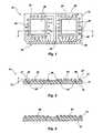
- FIG. 1is a top view of an exemplary circuit board according to the present invention, which includes terminals that protrude from at least one surface thereof;
- FIG. 2is a cross-section taken along line 2 - 2 of FIG. 1 ;
- FIG. 3is a cross-sectional representation of another exemplary circuit board which includes a raised die-attach location
- FIG. 4is a top view of a circuit board with each recessed area thereof being positioned adjacent to a portion of the periphery of a die-attach location thereof;
- FIG. 5is a top view of an exemplary solder mask according to the present invention.
- FIG. 6is a top view of another exemplary solder mask of the present invention, each recessed area of which is located adjacent to only a portion of the periphery of a device-securing region thereof;
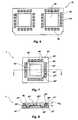
- FIG. 7is a top view of an exemplary circuit board assembly of the present invention which includes a circuit board and a solder mask;
- FIG. 8is a cross-section taken along line 8 - 8 of FIG. 7 ;
- FIG. 9is a top view of the circuit board assembly of FIG. 7 with a semiconductor device secured and electrically connected thereto;
- FIG. 10is cross-section taken along line 10 - 10 of FIG. 9 .
- circuit board 10includes a substantially planar substrate 12 with a plurality of die-attach locations 20 on at least one surface 14 thereof. Terminals 26 that correspond to each die-attach location 20 are positioned laterally adjacent thereto, adjacent to a periphery 22 of an area of surface 14 that will be occupied by a semiconductor device (not shown in FIG. 1 or FIG. 2 ) that will be secured to the corresponding die-attach location 20 . Circuit board 10 may also include at least one recessed area 24 located at least partially between each die-attach location 20 and at least some of its corresponding terminals 26 .
- Substrate 12 of circuit board 10may be formed from one or more layers of any suitable material (e.g., FR-4 resin).
- a plurality of conductive traces 28 that communicate with terminals 26may be carried upon one or both surfaces 14 and 16 of circuit board 10 , or internally thereby if substrate 12 comprises a multi-layer laminate structure.
- conductive traces 28are arranged in such a way as to establish communication between the leads of contacts (not shown in FIG. 1 or FIG. 2 ) of one or more of the semiconductor devices (also not shown in FIG. 1 or FIG.
- circuit board 10that are electrically connected thereto and other components, such as the peripheral componentry of a computer, other semiconductor devices, or the like, which may be carried by circuit board 10 or external thereto.
- conductive traces 28may extend to connective elements 29 of circuit board 10 , such as so-called “plug-and-play” type connectors, secondary terminals, conductive pins, or the like.
- circuit boards 10that include die-attach locations 20 with circuit traces 28 extending thereacross are also within the scope of the present invention.
- Each die-attach location 20 of circuit board 10is an area over which a semiconductor device is to be physically secured.
- bare semiconductor devices, packaged semiconductor devices, or multi-chip assembliesmay be secured over each die-attach location 20 .
- Die-attach locations 20may reside in substantially the same plane as their corresponding surface 14 , 16 , as shown in FIGS. 1 and 2 , or they may be raised somewhat relative to their corresponding surface 14 , 16 and, thus, reside in a different plane than that surface 14 , 16 , as depicted in FIG. 3 .
- Terminals 26 of circuit board 10are arranged on a surface 14 , 16 thereof in such a way as to facilitate the placement of intermediate conductive elements (not shown in FIG. 1 or FIG. 2 ), such as leads, bond wires, or conductive tape-automated bonding (TAB) elements comprising conductive traces carried upon a flexible dielectric substrate, in desired orientations between each terminal 26 and its corresponding bond pad of an adjacent semiconductor device (not shown in FIG. 1 or FIG. 2 ).
- Each terminal 26 of circuit board 10includes a connection surface 27 to which the corresponding intermediate conductive element is secured to establish electrical communication between that terminal 26 and its corresponding bond pad.
- At least some terminals 26 of circuit board 10protrude from the surface 14 , 16 upon which they are carried. Each such terminal 26 may protrude above its corresponding surface 14 , 16 by a distance D T that will prevent excess adhesive material (not shown in FIG. 1 or FIG. 2 ), which may be used for securing a semiconductor device to its corresponding die-attach location 20 , from flowing onto and, thus, contaminating connection surface 27 of that terminal 26 .
- connection surface 27 of each protruding terminal 26may be positioned at an elevation above its corresponding surface 14 , 16 that facilitates the connection of one or more intermediate conductive elements thereto.
- each connection surface 27may facilitate the use of shorter intermediate conductive elements between each terminal 26 and its corresponding bond pad or other contact of a semiconductor device as the semiconductor device is secured and electrically connected to circuit board 10 .
- Terminals 26 of circuit board 10may be fabricated by any suitable, known technique.
- an electrolytic processthat employs known dry film techniques and copper filling or plating may be used to form terminals 26 .
- each terminal 26may be plated with a material, such as gold or another so-called “noble metal”, nickel, or a combination of different plating layers, that may enhance the adhesion and electrical connection characteristics of an intermediate conductive element thereto.
- Such platingmay also be effected by known processes, such as by electrolytic, electroless, or immersion plating techniques.
- each recessed area 24may be sized and configured to receive at least some of the excess adhesive material that is forced outwardly from a die-attach location 20 of circuit board 10 as a semiconductor device is secured in position thereover.
- Each recessed area 24may substantially laterally surround its corresponding die-attach location 20 , as depicted in FIGS. 1 and 2 .
- one or more discrete recessed areas 24 ′may be positioned laterally around only portions of a corresponding die-attach location 20 .
- each recessed area 24 , 24 ′may extend into its corresponding die-attach location 20 so as to overlap periphery 22 and to extend at least partially beneath a semiconductor device when the semiconductor device is secured into position over that die-attach location 20 (see FIG. 10 ). Recessed areas 24 , 24 ′ may also laterally extend substantially to a periphery of each terminal 26 that corresponds to the corresponding die-attach location 20 , thereby effectively increasing the height of each such terminal 26 for purposes of preventing excess adhesive material from flowing onto and contaminating connection surface 27 thereof.
- solder mask 30for use on a surface of a circuit board, such as circuit board 10 of FIGS. 1 and 2 .
- Solder mask 30includes a plurality of dams 46 that are configured to laterally surround corresponding terminals (e.g., terminals 26 of circuit board 10 , shown in FIGS. 1 and 2 ) of the circuit board.
- solder mask 30may also include a plurality of device-securing regions 40 to which semiconductor devices may be secured. Also, if solder mask 30 includes one or more device-securing regions 40 , it may also include at least one recessed area 44 adjacent to each device-securing region 40 .
- Solder mask 30is configured to prevent solder or another electrically conductive joint-forming material (e.g., a conductive elastomer, conductor-filled epoxy, etc.) (not shown) from contacting various features of a circuit board.
- solder mask 30prevents such conductive joint-forming materials from damaging the circuit board, as well as from wetting and, thus, adhering to and potentially causing electrical shorting between electrically conductive features of the circuit board or structures carried thereby, such as conductive traces of the circuit board, connective elements of the circuit board, and devices that have already been secured to the circuit board, as well as other terminals of the circuit board to which bond wires or conductive TAB elements are to be subsequently secured.
- Each dam 46 of solder mask 30contacts at least a portion of a periphery of a corresponding terminal of the circuit board (e.g., a terminal 26 of circuit board 10 ) so as to prevent solder from flowing between that dam 46 and its corresponding, adjacent terminal 26 . Also, the distance D D ( FIG. 8 ) each dam 46 protrudes above a laterally adjacent location of solder mask 30 prevents excess quantities of the adhesive material (not shown in FIG. 5 ) which is used to secure a semiconductor device (not shown in FIG. 5 ) to the circuit board over which solder mask 30 is positioned from flowing onto and, thus, from contaminating its corresponding terminals.
- each dam 46 ′′may include a laterally extending ledge 47 which is configured to extend over a peripheral edge of the connection surface of its corresponding terminal (e.g., connection surface 27 of terminal 26 ).
- Ledge 47may be configured to further prevent excess adhesive material from flowing onto and contaminating the connection surface without impeding connection of an intermediate conductive element thereto.
- the height H of ledge 47 relative to the connection surface 27 of the adjacent terminal 26may be small enough, and the area and shape of the connection surface 27 that is exposed through or laterally beyond ledge 47 may be large enough, to permit connection equipment (e.g., a wire bonding capillary) to access the connection surface.
- each dam 46is configured to surround the entire periphery of its corresponding terminal. Also, each dam 46 includes a ledge 47 ( FIG. 10 ) that extends over the entire peripheral edge of the connection surface of its corresponding terminal.
- Each device-securing region 40 of solder mask 30is positionable over a corresponding die-attach location of the circuit board (e.g., a die-attach location 20 of circuit board 10 ) over which solder mask 30 is to be positioned. Dams 46 of solder mask 30 that correspond to a particular device-securing region 40 may be positioned laterally adjacent to that device-securing region 40 .
- Each device-securing region 40 of solder mask 30is configured to receive a semiconductor device, such as a bare semiconductor device, a packaged semiconductor device, or a multi-chip assembly, and to have the semiconductor device secured thereto.
- a semiconductor devicesuch as a bare semiconductor device, a packaged semiconductor device, or a multi-chip assembly
- an adhesive materialsuch as a suitable epoxy, thermoset resin, or pressure-sensitive adhesive, may be used to secure a semiconductor device to a device-securing region 40 of solder mask 30 .
- the adhesive materialis in a liquid or semisolid state as the semiconductor device is positioned over device-securing region 40 , some of the adhesive material may be forced from between the semiconductor device and device-securing region 40 , laterally beyond an outer periphery of the semiconductor device, and toward dams 46 and their corresponding terminals of the circuit board that underlies solder mask 30 .
- one or more recessed areas 44may be provided between each device-securing region 40 and at least some of its corresponding dams 46 .
- Each recessed area 44may have dimensions that are configured to receive substantially all of the excess adhesive material that is forced from between a semiconductor device and the adjacent device-securing region 40 when the semiconductor device is secured to device-securing region 40 .
- a single recessed area 44laterally surrounds an outer periphery 42 of each device-securing region 40 .
- one or more recessed areas 44 ′may be positioned adjacent to only portions of an outer periphery 42 of a corresponding device-securing region 40 of solder mask 30 .
- one or more recessed areas 44 ′′may extend beneath the location at which an outer periphery of a semiconductor device will be positioned when the semiconductor device is secured to device-securing region 40 .
- Solder mask 30may comprise a preformed element that is configured to be aligned relative to, positioned over, and secured (e.g., with an adhesive material) to a complementary circuit board. Alternatively, solder mask 30 may be formed on the circuit board.
- solder mask 30may be formed either separately from or on a circuit board.
- known photolithography techniqueswhich include the use of a liquid photoresist material, a pattern on a reticle to be copied to a layer of the photoresist material, radiation of a suitable wavelength for exposing selected regions of the layer of photoresist material through the reticle, and resist-developing chemicals that are appropriate for use with the photoresist material. Dry film photoresist materials are also known and suitable for use in the present invention may be employed.
- stereolithographic techniquesmay be used to form solder mask 30 from one or more layers of a photocurable polymer by selectively exposing regions of each layer of photocurable polymer, one layer at a time, to cure the selectively exposed regions.
- FIGS. 7 and 8an example of a circuit board assembly 1 is depicted which includes a circuit board 10 ′′ and a solder mask 30 ′′ that incorporate teachings of the present invention.
- circuit board 10 ′′includes a substrate 12 ′′ with a single die-attach location 20 ′′ on a substantially planar surface 14 ′′ thereof.
- a plurality of terminals 26 ′′is positioned around and adjacent to a periphery 23 ′′ of die-attach location 20 ′′.
- Each of terminals 26 ′′protrudes from surface 14 ′′ to substantially the same elevation relative to (e.g., over) surface 14 ′′.
- Solder mask 30 ′′which substantially covers surface 14 ′′, includes a single device-securing region 40 ′′ that is aligned with and positioned over at least a portion of die-attach location 20 ′′ of circuit board 10 ′′.
- dams 46 ′′ of solder mask 30 ′′are aligned with and positioned laterally around corresponding terminals 26 ′′ of circuit board 10 ′′.
- dams 46 ′′may substantially laterally surround terminals 26 ′′, with only connection surface 27 ′′ of each terminal 26 ′′ or a portion thereof being exposed through each dam 46 ′′.
- a recessed area 44 ′′is positioned between each peripheral edge 43 ′′ of device-securing region 40 ′′ and dams 46 ′′ that are located adjacent to that peripheral edge 43 ′′.
- each recessed area 44 ′′is positioned over circuit board 10 ′′ so as to extend laterally from a die-attach location 20 ′′ thereof to terminals 26 ′′ that correspond to that die-attach location 20 ′′.
- FIGS. 9 and 10assembly and electrical connection of semiconductor devices 50 with a strip 2 comprising a plurality of unsevered circuit board assemblies 1 are described.
- Semiconductor device 50may comprise a bare semiconductor die, as depicted, or a packaged semiconductor device. Also, semiconductor device 50 may comprise a single semiconductor die or a multi-chip assembly. A quantity of a suitable adhesive material 60 , such as a two-stage epoxy, a thermoset resin, or a pressure-sensitive adhesive material, may be applied to one or both of a bottom surface 52 of a semiconductor device 50 (i.e., the back side of the depicted semiconductor die) and a device-securing region 40 ′′ of solder mask 30 ′′.
- a suitable adhesive material 60such as a two-stage epoxy, a thermoset resin, or a pressure-sensitive adhesive material
- the volume defined by recessed areas 44 ′′, outer periphery 54 of semiconductor device 50 , and dams 46 ′′ of solder mask 30 ′′is preferably sufficient to receive substantially all of the excess adhesive material 60 forced from between semiconductor device 50 and device-securing region 40 ′′ of solder mask 30 ′′.
- this collective volumepreferably prevents adhesive material 60 from flowing onto exposed portions of connection surfaces 27 ′′ of adjacent terminals 26 ′′.
- any combination of raised terminals 26 , 26 ′′ and dams 46 , 46 ′′, recessed areas 24 , 24 ′ of a circuit board 10 , 10 ′′ and recessed areas 44 , 44 ′′ of a solder mask 30 , 30 ′′ of the present inventionmay prevent adhesive material 60 from contaminating connection surfaces 27 , 27 ′′ of terminals 26 , 26 ′′. Accordingly, each of these features of the present invention facilitates the placement of terminals 26 , 26 ′′ in closer proximity to their corresponding die-attach location 20 , 20 ′′ than the terminals of conventional circuit boards may be positioned relative to their corresponding die-attach locations.
- adhesive material 60if a curable material, may be partially or substantially cured, as appropriate for the type of adhesive material 60 used, to securely maintain the position of semiconductor device 50 on device-securing region 40 ′′.
- intermediate conductive elements 70such as the bond wires that are shown, leads, or conductive TAB elements carried by a dielectric film, may be positioned or formed between bond pads 56 of semiconductor device 50 and their corresponding terminals 26 ′′ of circuit board 10 ′′.
- semiconductor device 50 , intermediate conductive elements 70 , and, optionally, circuit board 10 ′′may be fully or partially encapsulated, as known in the art.
- a so-called “glob top” type encapsulant material 80may be disposed on semiconductor device 50 and intermediate conductive elements 70 ( FIG. 8 ).
- semiconductor device 50 , intermediate conductive elements 70 , and at least adjacent portions of circuit board 10 ′′may be encapsulated in a molded package.
Landscapes
- Engineering & Computer Science (AREA)
- Microelectronics & Electronic Packaging (AREA)
- Computer Hardware Design (AREA)
- Power Engineering (AREA)
- Physics & Mathematics (AREA)
- Condensed Matter Physics & Semiconductors (AREA)
- General Physics & Mathematics (AREA)
- Manufacturing & Machinery (AREA)
- Electric Connection Of Electric Components To Printed Circuits (AREA)
- Wire Bonding (AREA)
Abstract
Description
- This application is a continuation of application Ser. No. 10/120,169 filed Apr. 10, 2002, now U.S. Pat. No. 6,787,923, issued Sep. 7, 2004.
- 1. Field of the Invention
- The present invention relates generally to solder masks for use on carrier substrates and, more particularly, to solder masks that are configured to prevent excess adhesive material from contacting or covering terminals of carrier substrates. In addition, the present invention relates to carrier substrates including such solder masks and to semiconductor device assemblies and packages including the carrier substrates. The present invention also relates to methods for designing solder masks to be used on carrier substrates, to methods for forming solder masks on carrier substrates, and to methods for connecting semiconductor devices to carrier substrates.
- 2. Background of Related Art
- Circuit boards and other carrier substrates have long been employed to establish electrical communication between bond pads of semiconductor dice and other electronic components, including those carried by the circuit board and components that are external to the circuit board.
- Conventionally, relatively small circuit boards have been used to package one or more semiconductor dice, which protects the dice and provides a semiconductor device package that includes a standardized connection pattern, regardless of the arrangement of bond pads of each semiconductor die of such a package. These circuit boards are often referred to in the art as “interposers.” In the state of the art, the dimensions of interposers are approaching the corresponding dimensions of the semiconductor dice to be secured thereto, with the result being a continuous decrease in the sizes of semiconductor device packages, many of which are so-called “chip-scale packages” exhibiting dimensions that are the same as or only slightly larger than those of the die thereof.
- Nonetheless, when conventional wire bonding processes are used to electrically connect bond pads of a semiconductor die to corresponding contacts, or terminals, of an interposer to which the semiconductor die is back bonded, the terminals of the interposer must be positioned outside of the outer periphery of the semiconductor die. This requirement prevents a reduction in the size of these interposers to dimensions that are substantially the same as those of the semiconductor die to be secured thereto and carried thereby.
- Moreover, in order to securely attach a semiconductor die to the circuit board, it is typically desirable that a sufficient amount of adhesive material be used to form a confluent adhesive layer adjacent to the back side of the semiconductor die and a fillet around the entire outer periphery of the semiconductor die. Some excess adhesive material is typically required to adhere the semiconductor die and the circuit board to one another in this manner. When excess adhesive material is used, however, some of the adhesive material may flow outward from the semiconductor die, beyond the desired location for a fillet, and contaminate the connection surfaces of adjacent terminals, which are located at the same elevation as or just above a surface of the circuit board. If the connection surfaces of the terminals become contaminated in this manner, intermediate conductive elements, such as bond wires, may not adhere thereto or form an effective electrical connection, which may ultimately reduce the reliability of the packaged semiconductor device, or cause electrical shorting and failure of the packaged semiconductor device.
- Larger circuit boards, such as so-called “motherboards” and the substrates of so-called “plug-and-play” devices or cards, may be configured to carry a plurality of semiconductor devices. As with interposers, the trend with such larger circuit boards is also toward ever-decreasing sizes and ever-increasing densities. Consequently, contamination of the connection surfaces of terminals by adhesive material is increasingly encountered when semiconductor devices are assembled with larger circuit boards.
- Solder masks are often used on circuit boards to facilitate the formation of solder balls or bumps on selected terminals of the circuit boards while protecting other features thereof and preventing solder from wetting and adhering to other features of the circuit board. The solder masks that are used on circuit boards are typically fabricated from photoresists, using known photolithography processes. These solder masks may be left in place while semiconductor devices and other components are secured and electrically connected to the circuit board. Thus, a semiconductor device may be secured to a solder mask which is, in turn, secured to the circuit board to which the semiconductor device is to be electrically connected.
- When conventional solder masks are used on conventional circuit boards, a portion of the adhesive material that secures a semiconductor device to the solder mask may still flow laterally outward, beyond the outer periphery of the semiconductor device and onto connection surfaces of the adjacent terminals of the circuit board.
- Some solder masks have been configured with recesses to receive some of the excess adhesive material. Nonetheless, these recesses typically do not have great enough volumes to contain all of the excess adhesive material that is forced from beneath a semiconductor device as the semiconductor device is secured to the solder mask and, thus, to the circuit board. Consequently, the terminals of circuit boards are typically spaced a sufficient distance away from the location at which the outer periphery of a semiconductor device to be secured to the circuit board is to be positioned that the connection surfaces thereof will not be contaminated by adhesive material. Such positioning of the terminals undesirably requires that the circuit board include additional real estate, which prevents a reduction in the dimensions of the circuit board.
- The inventors are not aware of any carrier substrates or solder masks therefor that are configured to prevent adhesive material from flowing onto the connection surfaces of the carrier substrate terminals while reducing the dimensions of the carrier substrate.
- The present invention includes a solder mask for use on a carrier substrate, such as a circuit board. The solder mask is configured to receive adhesive and prevent the same from contacting or otherwise covering connection surfaces of the terminals of the circuit board or other carrier substrate.
- A solder mask according to the present invention includes semiconductor device-securing regions and may include recesses adjacent to the device-securing regions and which are configured to receive adhesive material, dams that are configured to laterally surround terminals of the circuit board, or a combination thereof. If the solder mask includes one or more recesses, or recessed areas, each recess may extend partially through the solder mask or completely therethrough. The collective volume defined between the outer periphery of a semiconductor device positioned upon a particular device-securing region of the solder mask and the solder dams and/or recesses that are adjacent thereto may receive substantially all of the excess adhesive material that is used to secure the semiconductor device to that supporting region. Accordingly, the height at which the supporting region positions a semiconductor device, as well as the depths and lateral dimensions of the recesses, may be configured to provide a volume that will receive excess adhesive.
- In addition, one or more of the solder dams of the solder mask may extend laterally over a peripheral portion of the connection surface of the terminal around which it is positioned. The laterally extending regions of each such solder dam may also provide additional surface area over which adhesive material may spread before spilling over onto the corresponding terminal of the circuit board.
- A circuit board upon which the solder mask is configured to be disposed may include terminals that protrude from, or are raised or elevated relative to, a surface thereof, increasing the volume within which adhesive material may be received. The distance the terminals protrude from the surface of the circuit board may provide a particular, desired volume between their corresponding solder dams and the location at which the outer periphery of a semiconductor device secured over the circuit board will be positioned. As an increased volume of adhesive material may be received between raised terminals and the location at which the outer periphery of a semiconductor device will be positioned, the terminals may be placed closer to their corresponding die-attach location than the terminals of conventional circuit boards and interposers. In addition, the connection surfaces of the terminals may be located at an elevation that is closer to the elevation at which the bond pads or other contacts of a semiconductor device are positioned over the circuit board. As a result of one or both of the closer spacing and raised elevation of the raised terminals, the raised terminals of a circuit board that incorporates teachings of the present invention may facilitate the use of shorter intermediate conductive elements between bond pads or other contacts of a semiconductor device and their corresponding terminals of the circuit board.
- As used herein, the term “circuit board” is not limited to particular structures such as conventional FR-4 resin boards but encompasses any conductor-carrying, substantially planar substrate or other die support member formed of any suitable material, including without limitation conductor-carrying laminates formed of various materials, silicon or glass substrates with deposited (as by photolithography) conductors, ceramic substrates and other suitable conductor carriers as known in the art. Further, the term “circuit board” includes and encompasses all types of single-die and multi-dice assemblies, such as multi-chip modules (MCMs) including different types of dice or the same die type, the latter being exemplified by single in-line memory modules (SIMMs) or dual in-line memory modules (DIMMs).
- Known techniques, including the use of adhesive material and positioning one or more semiconductor devices over the circuit board and in contact with the adhesive material, may be used to secure a semiconductor device to a circuit board carrying a solder mask according to the present invention. Upon being brought into contact with the adhesive material, positive pressure exerted by the positioning device and/or gravity may cause adhesive material between a support region of the solder mask on the circuit board and the semiconductor device to flow laterally outward, beyond an outer periphery of the support region and/or the semiconductor device. A receptacle formed at least in part by the solder mask will receive adhesive that is forced outward during placement of the semiconductor device. The volume of each adhesive receptacle, as well as the heights of the solder dams of the solder mask that laterally surround corresponding terminals of the circuit board, prevent adhesive material from contaminating the terminals.
- A semiconductor device assembly incorporating teachings of the present invention includes a circuit board with the solder mask thereon, as well as at least one semiconductor device positioned over and secured to a corresponding support region of the solder mask. Contacts of the semiconductor device may be electrically connected to corresponding terminals of the circuit board by way of intermediate conductive elements, such as leads, bond wires, and conductive tape-automated bond (TAB) elements carried by a dielectric film. The semiconductor device assembly may also be partially or fully encapsulated.
- The present invention also includes methods for designing circuit boards and solder masks to be used on circuit boards. The circuit boards, solder masks, or combinations thereof are configured to prevent excess adhesive material from contaminating the connection surfaces of circuit board terminals, while facilitating the placement of circuit board terminals more closely to the location at which the outer periphery of a semiconductor device will be located than the terminals of a conventional circuit board may be placed relative to the location at which the outer periphery of a semiconductor device thereon will be located.
- A method for designing a solder mask in accordance with the present invention includes configuring at least one device-securing region and at least one corresponding recess or a plurality of dams laterally adjacent thereto. Alternatively, a combination of dams and recesses may be configured, with the dams being located adjacent to at least one recess, opposite from the corresponding device-securing region. The heights of the at least one device-securing region and the solder dams that correspond thereto, as well as the depth and lateral dimensions of the at least one corresponding recess, may be configured to provide a desired adhesive receptacle volume.
- Additionally, the present invention includes a method for designing a circuit board to minimize contamination of the terminals thereof by excess adhesive. Such a method includes configuring terminals of the circuit board to protrude from a surface of the circuit board a distance that will provide a desired adhesive receptacle volume laterally between the terminals and a corresponding semiconductor device once the semiconductor device has been secured to the circuit board, while facilitating the connection of intermediate conductive elements to the terminals after the semiconductor device has been secured to the circuit board.
- Other features and advantages of the present invention will become apparent to those of ordinary skill in the art through consideration of the ensuing description, the accompanying drawings, and the appended claims.
- In the drawings, which depict various aspects of exemplary embodiments of the present invention:
FIG. 1 is a top view of an exemplary circuit board according to the present invention, which includes terminals that protrude from at least one surface thereof;FIG. 2 is a cross-section taken along line2-2 ofFIG. 1 ;FIG. 3 is a cross-sectional representation of another exemplary circuit board which includes a raised die-attach location;FIG. 4 is a top view of a circuit board with each recessed area thereof being positioned adjacent to a portion of the periphery of a die-attach location thereof;FIG. 5 is a top view of an exemplary solder mask according to the present invention;FIG. 6 is a top view of another exemplary solder mask of the present invention, each recessed area of which is located adjacent to only a portion of the periphery of a device-securing region thereof;FIG. 7 is a top view of an exemplary circuit board assembly of the present invention which includes a circuit board and a solder mask;FIG. 8 is a cross-section taken along line8-8 ofFIG. 7 ;FIG. 9 is a top view of the circuit board assembly ofFIG. 7 with a semiconductor device secured and electrically connected thereto; andFIG. 10 is cross-section taken along line10-10 ofFIG. 9 .- With reference to
FIGS. 1 and 2 , an exemplary embodiment of acircuit board 10 is depicted which incorporates teachings of the present invention. The depictedcircuit board 10 includes a substantiallyplanar substrate 12 with a plurality of die-attachlocations 20 on at least onesurface 14 thereof.Terminals 26 that correspond to each die-attachlocation 20 are positioned laterally adjacent thereto, adjacent to aperiphery 22 of an area ofsurface 14 that will be occupied by a semiconductor device (not shown inFIG. 1 orFIG. 2 ) that will be secured to the corresponding die-attachlocation 20.Circuit board 10 may also include at least one recessedarea 24 located at least partially between each die-attachlocation 20 and at least some of itscorresponding terminals 26. Substrate 12 ofcircuit board 10 may be formed from one or more layers of any suitable material (e.g., FR-4 resin). In addition toterminals 26, a plurality ofconductive traces 28 that communicate withterminals 26 may be carried upon one or bothsurfaces circuit board 10, or internally thereby ifsubstrate 12 comprises a multi-layer laminate structure. As is well known in the art,conductive traces 28 are arranged in such a way as to establish communication between the leads of contacts (not shown inFIG. 1 orFIG. 2 ) of one or more of the semiconductor devices (also not shown inFIG. 1 orFIG. 2 ) that are electrically connected thereto and other components, such as the peripheral componentry of a computer, other semiconductor devices, or the like, which may be carried bycircuit board 10 or external thereto. To establish communication between the leads or contacts of a semiconductor device that has been secured tocircuit board 10 and componentry external tocircuit board 10, conductive traces28 may extend toconnective elements 29 ofcircuit board 10, such as so-called “plug-and-play” type connectors, secondary terminals, conductive pins, or the like.- Although it is currently preferred that conductive traces28 do not extend across a
surface circuit board 10 in the area of a die-attachlocation 20,circuit boards 10 that include die-attachlocations 20 with circuit traces28 extending thereacross are also within the scope of the present invention. - Each die-attach
location 20 ofcircuit board 10 is an area over which a semiconductor device is to be physically secured. By way of example only, bare semiconductor devices, packaged semiconductor devices, or multi-chip assemblies may be secured over each die-attachlocation 20. Die-attachlocations 20 may reside in substantially the same plane as their correspondingsurface FIGS. 1 and 2 , or they may be raised somewhat relative to theircorresponding surface surface FIG. 3 . Terminals 26 ofcircuit board 10 are arranged on asurface FIG. 1 orFIG. 2 ), such as leads, bond wires, or conductive tape-automated bonding (TAB) elements comprising conductive traces carried upon a flexible dielectric substrate, in desired orientations between each terminal26 and its corresponding bond pad of an adjacent semiconductor device (not shown inFIG. 1 orFIG. 2 ). Eachterminal 26 ofcircuit board 10 includes aconnection surface 27 to which the corresponding intermediate conductive element is secured to establish electrical communication between that terminal26 and its corresponding bond pad.- At least some
terminals 26 ofcircuit board 10 protrude from thesurface surface FIG. 1 orFIG. 2 ), which may be used for securing a semiconductor device to its corresponding die-attachlocation 20, from flowing onto and, thus, contaminatingconnection surface 27 of that terminal26. In addition,connection surface 27 of each protrudingterminal 26 may be positioned at an elevation above its correspondingsurface connection surface 27, as well as the possibly closer positioning of each terminal26 relative to is corresponding die-attachlocation 20, may facilitate the use of shorter intermediate conductive elements between each terminal26 and its corresponding bond pad or other contact of a semiconductor device as the semiconductor device is secured and electrically connected tocircuit board 10. Terminals 26 ofcircuit board 10 may be fabricated by any suitable, known technique. By way of example only, an electrolytic process that employs known dry film techniques and copper filling or plating may be used to formterminals 26. Also, each terminal26 may be plated with a material, such as gold or another so-called “noble metal”, nickel, or a combination of different plating layers, that may enhance the adhesion and electrical connection characteristics of an intermediate conductive element thereto. Such plating may also be effected by known processes, such as by electrolytic, electroless, or immersion plating techniques.- If
circuit board 10 also includes one or more recessedareas 24, each recessedarea 24 may be sized and configured to receive at least some of the excess adhesive material that is forced outwardly from a die-attachlocation 20 ofcircuit board 10 as a semiconductor device is secured in position thereover. Each recessedarea 24 may substantially laterally surround its corresponding die-attachlocation 20, as depicted inFIGS. 1 and 2 . Alternatively, as shown inFIG. 4 , one or more discrete recessedareas 24′ may be positioned laterally around only portions of a corresponding die-attachlocation 20. Further, each recessedarea location 20 so as to overlapperiphery 22 and to extend at least partially beneath a semiconductor device when the semiconductor device is secured into position over that die-attach location20 (seeFIG. 10 ). Recessedareas location 20, thereby effectively increasing the height of eachsuch terminal 26 for purposes of preventing excess adhesive material from flowing onto and contaminatingconnection surface 27 thereof. - Turning now to
FIG. 5 , an exemplary embodiment of asolder mask 30 for use on a surface of a circuit board, such ascircuit board 10 ofFIGS. 1 and 2 , is illustrated.Solder mask 30 includes a plurality ofdams 46 that are configured to laterally surround corresponding terminals (e.g.,terminals 26 ofcircuit board 10, shown inFIGS. 1 and 2 ) of the circuit board. As shown inFIG. 5 ,solder mask 30 may also include a plurality of device-securingregions 40 to which semiconductor devices may be secured. Also, ifsolder mask 30 includes one or more device-securingregions 40, it may also include at least one recessedarea 44 adjacent to each device-securingregion 40. Solder mask 30 is configured to prevent solder or another electrically conductive joint-forming material (e.g., a conductive elastomer, conductor-filled epoxy, etc.) (not shown) from contacting various features of a circuit board. Thus,solder mask 30 prevents such conductive joint-forming materials from damaging the circuit board, as well as from wetting and, thus, adhering to and potentially causing electrical shorting between electrically conductive features of the circuit board or structures carried thereby, such as conductive traces of the circuit board, connective elements of the circuit board, and devices that have already been secured to the circuit board, as well as other terminals of the circuit board to which bond wires or conductive TAB elements are to be subsequently secured.- Each
dam 46 ofsolder mask 30 contacts at least a portion of a periphery of a corresponding terminal of the circuit board (e.g., aterminal 26 of circuit board10) so as to prevent solder from flowing between thatdam 46 and its corresponding,adjacent terminal 26. Also, the distance DD(FIG. 8 ) eachdam 46 protrudes above a laterally adjacent location ofsolder mask 30 prevents excess quantities of the adhesive material (not shown inFIG. 5 ) which is used to secure a semiconductor device (not shown inFIG. 5 ) to the circuit board over whichsolder mask 30 is positioned from flowing onto and, thus, from contaminating its corresponding terminals. - As depicted in
FIG. 10 , eachdam 46″ may include a laterally extendingledge 47 which is configured to extend over a peripheral edge of the connection surface of its corresponding terminal (e.g.,connection surface 27 of terminal26).Ledge 47 may be configured to further prevent excess adhesive material from flowing onto and contaminating the connection surface without impeding connection of an intermediate conductive element thereto. Thus, the height H ofledge 47 relative to theconnection surface 27 of theadjacent terminal 26 may be small enough, and the area and shape of theconnection surface 27 that is exposed through or laterally beyondledge 47 may be large enough, to permit connection equipment (e.g., a wire bonding capillary) to access the connection surface. - As shown in
FIG. 5 , eachdam 46 is configured to surround the entire periphery of its corresponding terminal. Also, eachdam 46 includes a ledge47 (FIG. 10 ) that extends over the entire peripheral edge of the connection surface of its corresponding terminal. - Each device-securing
region 40 ofsolder mask 30 is positionable over a corresponding die-attach location of the circuit board (e.g., a die-attachlocation 20 of circuit board10) over whichsolder mask 30 is to be positioned.Dams 46 ofsolder mask 30 that correspond to a particular device-securingregion 40 may be positioned laterally adjacent to that device-securingregion 40. - Each device-securing
region 40 ofsolder mask 30 is configured to receive a semiconductor device, such as a bare semiconductor device, a packaged semiconductor device, or a multi-chip assembly, and to have the semiconductor device secured thereto. By way of example only, an adhesive material, such as a suitable epoxy, thermoset resin, or pressure-sensitive adhesive, may be used to secure a semiconductor device to a device-securingregion 40 ofsolder mask 30. If the adhesive material is in a liquid or semisolid state as the semiconductor device is positioned over device-securingregion 40, some of the adhesive material may be forced from between the semiconductor device and device-securingregion 40, laterally beyond an outer periphery of the semiconductor device, and towarddams 46 and their corresponding terminals of the circuit board that underliessolder mask 30. - To further reduce the likelihood that such excess adhesive material will flow over
dams 46 and contaminate the connection surfaces of their corresponding terminals, one or more recessedareas 44 may be provided between each device-securingregion 40 and at least some of itscorresponding dams 46. Each recessedarea 44 may have dimensions that are configured to receive substantially all of the excess adhesive material that is forced from between a semiconductor device and the adjacent device-securingregion 40 when the semiconductor device is secured to device-securingregion 40. - As shown in
FIG. 5 , a single recessedarea 44 laterally surrounds anouter periphery 42 of each device-securingregion 40. Alternatively, as depicted inFIG. 6 , one or more recessedareas 44′ may be positioned adjacent to only portions of anouter periphery 42 of a corresponding device-securingregion 40 ofsolder mask 30. In either event, as shown inFIG. 10 , one or more recessedareas 44″ may extend beneath the location at which an outer periphery of a semiconductor device will be positioned when the semiconductor device is secured to device-securingregion 40. Solder mask 30 may comprise a preformed element that is configured to be aligned relative to, positioned over, and secured (e.g., with an adhesive material) to a complementary circuit board. Alternatively,solder mask 30 may be formed on the circuit board.- A variety of known, suitable processes may be employed to form
solder mask 30 either separately from or on a circuit board. By way of example only, known photolithography techniques, which include the use of a liquid photoresist material, a pattern on a reticle to be copied to a layer of the photoresist material, radiation of a suitable wavelength for exposing selected regions of the layer of photoresist material through the reticle, and resist-developing chemicals that are appropriate for use with the photoresist material. Dry film photoresist materials are also known and suitable for use in the present invention may be employed. As another example, stereolithographic techniques may be used to formsolder mask 30 from one or more layers of a photocurable polymer by selectively exposing regions of each layer of photocurable polymer, one layer at a time, to cure the selectively exposed regions. - Turning now to
FIGS. 7 and 8 , an example of acircuit board assembly 1 is depicted which includes acircuit board 10″ and asolder mask 30″ that incorporate teachings of the present invention. - As shown,
circuit board 10″ includes asubstrate 12″ with a single die-attachlocation 20″ on a substantiallyplanar surface 14″ thereof. A plurality ofterminals 26″ is positioned around and adjacent to aperiphery 23″ of die-attachlocation 20″. Each ofterminals 26″ protrudes fromsurface 14″ to substantially the same elevation relative to (e.g., over)surface 14″. Solder mask 30″, which substantially coverssurface 14″, includes a single device-securingregion 40″ that is aligned with and positioned over at least a portion of die-attachlocation 20″ ofcircuit board 10″. In addition,dams 46″ ofsolder mask 30″ are aligned with and positioned laterally around correspondingterminals 26″ ofcircuit board 10″. As shown,dams 46″ may substantially laterally surroundterminals 26″, withonly connection surface 27″ of each terminal26″ or a portion thereof being exposed through eachdam 46″. A recessedarea 44″ is positioned between eachperipheral edge 43″ of device-securingregion 40″ anddams 46″ that are located adjacent to thatperipheral edge 43″. Thus, each recessedarea 44″ is positioned overcircuit board 10″ so as to extend laterally from a die-attachlocation 20″ thereof toterminals 26″ that correspond to that die-attachlocation 20″.- In
FIGS. 9 and 10 , assembly and electrical connection ofsemiconductor devices 50 with astrip 2 comprising a plurality of unseveredcircuit board assemblies 1 are described. Semiconductor device 50 may comprise a bare semiconductor die, as depicted, or a packaged semiconductor device. Also,semiconductor device 50 may comprise a single semiconductor die or a multi-chip assembly. A quantity of a suitableadhesive material 60, such as a two-stage epoxy, a thermoset resin, or a pressure-sensitive adhesive material, may be applied to one or both of abottom surface 52 of a semiconductor device50 (i.e., the back side of the depicted semiconductor die) and a device-securingregion 40″ ofsolder mask 30″. As asemiconductor device 50 is positioned adjacent to (e.g., over) its corresponding device-securingregion 40″, someadhesive material 60 therebetween may be forced beyond anouter periphery 54 ofsemiconductor device 50, towarddams 46″ ofsolder mask 30″ and theircorresponding terminals 26″ ofcircuit board 10″. This excessadhesive material 60 is received within recessedareas 44″, as well as betweenouter periphery 54 ofsemiconductor device 50 anddams 46″ ofsolder mask 30″ that are positioned adjacent to associatedterminals 26″ ofcircuit board 10″. The volume defined by recessedareas 44″,outer periphery 54 ofsemiconductor device 50, anddams 46″ ofsolder mask 30″ is preferably sufficient to receive substantially all of the excessadhesive material 60 forced from betweensemiconductor device 50 and device-securingregion 40″ ofsolder mask 30″. Thus, this collective volume preferably preventsadhesive material 60 from flowing onto exposed portions of connection surfaces27″ ofadjacent terminals 26″.- Any combination of raised
terminals dams areas circuit board areas solder mask adhesive material 60 from contaminating connection surfaces27,27″ ofterminals terminals location - Once a
semiconductor device 50 has been positioned and properly oriented relative to the appropriate locations ofcircuit board 10″ andsolder mask 30″,adhesive material 60, if a curable material, may be partially or substantially cured, as appropriate for the type ofadhesive material 60 used, to securely maintain the position ofsemiconductor device 50 on device-securingregion 40″. In addition, intermediateconductive elements 70, such as the bond wires that are shown, leads, or conductive TAB elements carried by a dielectric film, may be positioned or formed betweenbond pads 56 ofsemiconductor device 50 and theircorresponding terminals 26″ ofcircuit board 10″. - Following the placement or formation of intermediate
conductive elements 70 betweenbond pads 56 ofsemiconductor device 50 and theircorresponding terminals 26″ ofcircuit board 10″,semiconductor device 50, intermediateconductive elements 70, and, optionally,circuit board 10″ may be fully or partially encapsulated, as known in the art. By way of example only, a so-called “glob top”type encapsulant material 80 may be disposed onsemiconductor device 50 and intermediate conductive elements70 (FIG. 8 ). Alternatively,semiconductor device 50, intermediateconductive elements 70, and at least adjacent portions ofcircuit board 10″ may be encapsulated in a molded package. - Although the foregoing description contains many specifics, these should not be construed as limiting the scope of the present invention, but merely as providing illustrations of some of the presently preferred embodiments. Similarly, other embodiments of the invention may be devised which do not depart from the spirit or scope of the present invention. Moreover, features from different embodiments of the invention may be employed in combination. The scope of the invention is, therefore, indicated and limited only by the appended claims and their legal equivalents, rather than by the foregoing description. All additions, deletions, and modifications to the invention, as disclosed herein, which fall within the meaning and scope of the claims are to be embraced thereby.
Claims (23)
Priority Applications (1)
| Application Number | Priority Date | Filing Date | Title |
|---|---|---|---|
| US10/936,304US7061124B2 (en) | 2002-04-02 | 2004-09-07 | Solder masks including dams for at least partially surrounding terminals of a carrier substrate and recessed areas positioned adjacent to the dams, and carrier substrates including such solder masks |
Applications Claiming Priority (4)
| Application Number | Priority Date | Filing Date | Title |
|---|---|---|---|
| SG200201827-3 | 2002-02-04 | ||
| SG200201827ASG107584A1 (en) | 2002-04-02 | 2002-04-02 | Solder masks for use on carrier substrates, carrier substrates and semiconductor device assemblies including such masks |
| US10/120,169US6787923B2 (en) | 2002-04-02 | 2002-04-10 | Solder masks for use on carrier substrates, carrier substrates and semiconductor device assemblies including such solder masks |
| US10/936,304US7061124B2 (en) | 2002-04-02 | 2004-09-07 | Solder masks including dams for at least partially surrounding terminals of a carrier substrate and recessed areas positioned adjacent to the dams, and carrier substrates including such solder masks |
Related Parent Applications (1)
| Application Number | Title | Priority Date | Filing Date |
|---|---|---|---|
| US10/120,169ContinuationUS6787923B2 (en) | 2002-04-02 | 2002-04-10 | Solder masks for use on carrier substrates, carrier substrates and semiconductor device assemblies including such solder masks |
Publications (2)
| Publication Number | Publication Date |
|---|---|
| US20050029676A1true US20050029676A1 (en) | 2005-02-10 |
| US7061124B2 US7061124B2 (en) | 2006-06-13 |
Family
ID=32923964
Family Applications (3)
| Application Number | Title | Priority Date | Filing Date |
|---|---|---|---|
| US10/120,169Expired - LifetimeUS6787923B2 (en) | 2002-04-02 | 2002-04-10 | Solder masks for use on carrier substrates, carrier substrates and semiconductor device assemblies including such solder masks |
| US10/642,908Expired - Fee RelatedUS7018871B2 (en) | 2002-04-02 | 2003-08-18 | Solder masks for use on carrier substrates, carrier substrates and semiconductor device assemblies including such solder masks, and methods |
| US10/936,304Expired - LifetimeUS7061124B2 (en) | 2002-04-02 | 2004-09-07 | Solder masks including dams for at least partially surrounding terminals of a carrier substrate and recessed areas positioned adjacent to the dams, and carrier substrates including such solder masks |
Family Applications Before (2)
| Application Number | Title | Priority Date | Filing Date |
|---|---|---|---|
| US10/120,169Expired - LifetimeUS6787923B2 (en) | 2002-04-02 | 2002-04-10 | Solder masks for use on carrier substrates, carrier substrates and semiconductor device assemblies including such solder masks |
| US10/642,908Expired - Fee RelatedUS7018871B2 (en) | 2002-04-02 | 2003-08-18 | Solder masks for use on carrier substrates, carrier substrates and semiconductor device assemblies including such solder masks, and methods |
Country Status (2)
| Country | Link |
|---|---|
| US (3) | US6787923B2 (en) |
| SG (1) | SG107584A1 (en) |
Cited By (2)
| Publication number | Priority date | Publication date | Assignee | Title |
|---|---|---|---|---|
| US20020199159A1 (en)* | 2001-06-22 | 2002-12-26 | Vinson Dong | Naked chip motherboard module |
| US8455989B2 (en) | 2011-07-01 | 2013-06-04 | Texas Instruments Incorporated | Package substrate having die pad with outer raised portion and interior recessed portion |
Families Citing this family (29)
| Publication number | Priority date | Publication date | Assignee | Title |
|---|---|---|---|---|
| US6297548B1 (en) | 1998-06-30 | 2001-10-02 | Micron Technology, Inc. | Stackable ceramic FBGA for high thermal applications |
| US7275925B2 (en)* | 2001-08-30 | 2007-10-02 | Micron Technology, Inc. | Apparatus for stereolithographic processing of components and assemblies |
| SG107584A1 (en) | 2002-04-02 | 2004-12-29 | Micron Technology Inc | Solder masks for use on carrier substrates, carrier substrates and semiconductor device assemblies including such masks |
| US7368391B2 (en) | 2002-04-10 | 2008-05-06 | Micron Technology, Inc. | Methods for designing carrier substrates with raised terminals |
| US6998334B2 (en) | 2002-07-08 | 2006-02-14 | Micron Technology, Inc. | Semiconductor devices with permanent polymer stencil and method for manufacturing the same |
| US6984545B2 (en)* | 2002-07-22 | 2006-01-10 | Micron Technology, Inc. | Methods of encapsulating selected locations of a semiconductor die assembly using a thick solder mask |
| US6900876B2 (en)* | 2003-02-13 | 2005-05-31 | Eastman Kodak Company | Process and structures for selective deposition of liquid-crystal emulsion |
| US7043830B2 (en) | 2003-02-20 | 2006-05-16 | Micron Technology, Inc. | Method of forming conductive bumps |
| JP4340578B2 (en)* | 2004-04-09 | 2009-10-07 | 富士通株式会社 | Component mounting board and component mounting structure |
| TWI253888B (en)* | 2004-12-09 | 2006-04-21 | Advanced Semiconductor Eng | Method of packaging flip chip and method of forming pre-solders on substrate thereof |
| US8294279B2 (en)* | 2005-01-25 | 2012-10-23 | Megica Corporation | Chip package with dam bar restricting flow of underfill |
| JP4885123B2 (en)* | 2005-03-25 | 2012-02-29 | シャープ株式会社 | Semiconductor device and manufacturing method thereof |
| US7323675B2 (en)* | 2005-09-21 | 2008-01-29 | Sigurd Microelectronics Corp. | Packaging structure of a light-sensing device with a spacer wall |
| US7511359B2 (en)* | 2005-12-29 | 2009-03-31 | Intel Corporation | Dual die package with high-speed interconnect |
| KR100833194B1 (en)* | 2006-12-19 | 2008-05-28 | 삼성전자주식회사 | Semiconductor package and manufacturing method in which wiring layer of semiconductor chip is directly connected to substrate |
| US20090108473A1 (en)* | 2007-10-26 | 2009-04-30 | Broadcom Corporation | Die-attach material overflow control for die protection in integrated circuit packages |
| JP2009206286A (en)* | 2008-02-27 | 2009-09-10 | Kyocera Corp | Printed circuit board and portable electronic equipment using the same |
| SG142321A1 (en) | 2008-04-24 | 2009-11-26 | Micron Technology Inc | Pre-encapsulated cavity interposer |
| DE102008034033B4 (en)* | 2008-07-22 | 2014-11-27 | Ust Umweltsensortechnik Gmbh | Microelectronic sensor component |
| JP5210839B2 (en)* | 2008-12-10 | 2013-06-12 | 新光電気工業株式会社 | Wiring board and manufacturing method thereof |
| WO2010089814A1 (en)* | 2009-02-04 | 2010-08-12 | パナソニック株式会社 | Semiconductor substrate structure and semiconductor device |
| KR101184006B1 (en)* | 2010-09-28 | 2012-09-19 | 삼성전기주식회사 | Printed circuit board and manufacturing method thereof |
| JP2014082468A (en)* | 2012-09-25 | 2014-05-08 | Canon Components Inc | Substrate member and method for manufacturing chip |
| US9497861B2 (en)* | 2012-12-06 | 2016-11-15 | Taiwan Semiconductor Manufacturing Company, Ltd. | Methods and apparatus for package with interposers |
| US8994176B2 (en) | 2012-12-13 | 2015-03-31 | Taiwan Semiconductor Manufacturing Company, Ltd. | Methods and apparatus for package with interposers |
| US10056294B2 (en)* | 2013-12-02 | 2018-08-21 | Maxim Integrated Products, Inc. | Techniques for adhesive control between a substrate and a die |
| US20150197062A1 (en)* | 2014-01-12 | 2015-07-16 | Zohar SHINAR | Method, device, and system of three-dimensional printing |
| US20150201500A1 (en)* | 2014-01-12 | 2015-07-16 | Zohar SHINAR | System, device, and method of three-dimensional printing |
| JP6815875B2 (en)* | 2017-01-19 | 2021-01-20 | Ngkエレクトロデバイス株式会社 | Wiring boards and electronic component storage packages and electronic devices |
Citations (25)
| Publication number | Priority date | Publication date | Assignee | Title |
|---|---|---|---|---|
| US5041395A (en)* | 1989-04-07 | 1991-08-20 | Sgs-Thomson Microelectronics S.A. | Method of encapsulating an integrated circuit using a punched metal grid attached to a perforated dielectric strip |
| US5196371A (en)* | 1989-12-18 | 1993-03-23 | Epoxy Technology, Inc. | Flip chip bonding method using electrically conductive polymer bumps |
| US5239131A (en)* | 1992-07-13 | 1993-08-24 | Olin Corporation | Electronic package having controlled epoxy flow |
| US5336931A (en)* | 1993-09-03 | 1994-08-09 | Motorola, Inc. | Anchoring method for flow formed integrated circuit covers |
| US5409863A (en)* | 1993-02-19 | 1995-04-25 | Lsi Logic Corporation | Method and apparatus for controlling adhesive spreading when attaching an integrated circuit die |
| US5558267A (en)* | 1995-03-31 | 1996-09-24 | Texas Instruments Incorporated | Moat for die pad cavity in bond station heater block |
| US5744084A (en)* | 1995-07-24 | 1998-04-28 | Lsi Logic Corporation | Method of improving molding of an overmolded package body on a substrate |
| US5917234A (en)* | 1994-12-09 | 1999-06-29 | Sony Corporation | Semiconductor device |
| US6020218A (en)* | 1997-01-28 | 2000-02-01 | Anam Semiconductor Inc. | Method of manufacturing ball grid array semiconductor package |
| US6232650B1 (en)* | 1997-07-30 | 2001-05-15 | Hitachi, Ltd. | Semiconductor device having a chip mounted on a flexible substrate with separated insulation layers to prevent short-circuiting |
| US6251488B1 (en)* | 1999-05-05 | 2001-06-26 | Optomec Design Company | Precision spray processes for direct write electronic components |
| US6259962B1 (en)* | 1999-03-01 | 2001-07-10 | Objet Geometries Ltd. | Apparatus and method for three dimensional model printing |
| US6268584B1 (en)* | 1998-01-22 | 2001-07-31 | Optomec Design Company | Multiple beams and nozzles to increase deposition rate |
| US20010010947A1 (en)* | 1999-11-22 | 2001-08-02 | Advanced Semiconductor Engineering, Inc. | Film ball grid array (BGA) semiconductor package |
| US6331451B1 (en)* | 1999-11-05 | 2001-12-18 | Amkor Technology, Inc. | Methods of making thin integrated circuit device packages with improved thermal performance and substrates for making the packages |
| US6391251B1 (en)* | 1999-07-07 | 2002-05-21 | Optomec Design Company | Forming structures from CAD solid models |
| US6395998B1 (en)* | 2000-09-13 | 2002-05-28 | International Business Machines Corporation | Electronic package having an adhesive retaining cavity |
| US6400007B1 (en)* | 2001-04-16 | 2002-06-04 | Kingpak Technology Inc. | Stacked structure of semiconductor means and method for manufacturing the same |
| US6426565B1 (en)* | 2000-03-22 | 2002-07-30 | International Business Machines Corporation | Electronic package and method of making same |
| US6448507B1 (en)* | 2000-06-28 | 2002-09-10 | Advanced Micro Devices, Inc. | Solder mask for controlling resin bleed |
| US6479887B1 (en)* | 1998-08-31 | 2002-11-12 | Amkor Technology, Inc. | Circuit pattern tape for wafer-scale production of chip size semiconductor packages |
| US20030052419A1 (en)* | 2001-09-18 | 2003-03-20 | Hitachi, Ltd. | Semiconductor device and method of manufacturing the same |
| US6593220B1 (en)* | 2002-01-03 | 2003-07-15 | Taiwan Semiconductor Manufacturing Company | Elastomer plating mask sealed wafer level package method |
| US6608375B2 (en)* | 2001-04-06 | 2003-08-19 | Oki Electric Industry Co., Ltd. | Semiconductor apparatus with decoupling capacitor |
| US6787923B2 (en)* | 2002-04-02 | 2004-09-07 | Micron Technology, Inc. | Solder masks for use on carrier substrates, carrier substrates and semiconductor device assemblies including such solder masks |
Family Cites Families (3)
| Publication number | Priority date | Publication date | Assignee | Title |
|---|---|---|---|---|
| US20020171177A1 (en) | 2001-03-21 | 2002-11-21 | Kritchman Elisha M. | System and method for printing and supporting three dimensional objects |
| US7275925B2 (en) | 2001-08-30 | 2007-10-02 | Micron Technology, Inc. | Apparatus for stereolithographic processing of components and assemblies |
| US20030151167A1 (en) | 2002-01-03 | 2003-08-14 | Kritchman Eliahu M. | Device, system and method for accurate printing of three dimensional objects |
- 2002
- 2002-04-02SGSG200201827Apatent/SG107584A1/enunknown
- 2002-04-10USUS10/120,169patent/US6787923B2/ennot_activeExpired - Lifetime
- 2003
- 2003-08-18USUS10/642,908patent/US7018871B2/ennot_activeExpired - Fee Related
- 2004
- 2004-09-07USUS10/936,304patent/US7061124B2/ennot_activeExpired - Lifetime
Patent Citations (25)
| Publication number | Priority date | Publication date | Assignee | Title |
|---|---|---|---|---|
| US5041395A (en)* | 1989-04-07 | 1991-08-20 | Sgs-Thomson Microelectronics S.A. | Method of encapsulating an integrated circuit using a punched metal grid attached to a perforated dielectric strip |
| US5196371A (en)* | 1989-12-18 | 1993-03-23 | Epoxy Technology, Inc. | Flip chip bonding method using electrically conductive polymer bumps |
| US5239131A (en)* | 1992-07-13 | 1993-08-24 | Olin Corporation | Electronic package having controlled epoxy flow |
| US5409863A (en)* | 1993-02-19 | 1995-04-25 | Lsi Logic Corporation | Method and apparatus for controlling adhesive spreading when attaching an integrated circuit die |
| US5336931A (en)* | 1993-09-03 | 1994-08-09 | Motorola, Inc. | Anchoring method for flow formed integrated circuit covers |
| US5917234A (en)* | 1994-12-09 | 1999-06-29 | Sony Corporation | Semiconductor device |
| US5558267A (en)* | 1995-03-31 | 1996-09-24 | Texas Instruments Incorporated | Moat for die pad cavity in bond station heater block |
| US5744084A (en)* | 1995-07-24 | 1998-04-28 | Lsi Logic Corporation | Method of improving molding of an overmolded package body on a substrate |
| US6020218A (en)* | 1997-01-28 | 2000-02-01 | Anam Semiconductor Inc. | Method of manufacturing ball grid array semiconductor package |
| US6232650B1 (en)* | 1997-07-30 | 2001-05-15 | Hitachi, Ltd. | Semiconductor device having a chip mounted on a flexible substrate with separated insulation layers to prevent short-circuiting |
| US6268584B1 (en)* | 1998-01-22 | 2001-07-31 | Optomec Design Company | Multiple beams and nozzles to increase deposition rate |
| US6479887B1 (en)* | 1998-08-31 | 2002-11-12 | Amkor Technology, Inc. | Circuit pattern tape for wafer-scale production of chip size semiconductor packages |
| US6259962B1 (en)* | 1999-03-01 | 2001-07-10 | Objet Geometries Ltd. | Apparatus and method for three dimensional model printing |
| US6251488B1 (en)* | 1999-05-05 | 2001-06-26 | Optomec Design Company | Precision spray processes for direct write electronic components |
| US6391251B1 (en)* | 1999-07-07 | 2002-05-21 | Optomec Design Company | Forming structures from CAD solid models |
| US6331451B1 (en)* | 1999-11-05 | 2001-12-18 | Amkor Technology, Inc. | Methods of making thin integrated circuit device packages with improved thermal performance and substrates for making the packages |
| US20010010947A1 (en)* | 1999-11-22 | 2001-08-02 | Advanced Semiconductor Engineering, Inc. | Film ball grid array (BGA) semiconductor package |
| US6426565B1 (en)* | 2000-03-22 | 2002-07-30 | International Business Machines Corporation | Electronic package and method of making same |
| US6448507B1 (en)* | 2000-06-28 | 2002-09-10 | Advanced Micro Devices, Inc. | Solder mask for controlling resin bleed |
| US6395998B1 (en)* | 2000-09-13 | 2002-05-28 | International Business Machines Corporation | Electronic package having an adhesive retaining cavity |
| US6608375B2 (en)* | 2001-04-06 | 2003-08-19 | Oki Electric Industry Co., Ltd. | Semiconductor apparatus with decoupling capacitor |
| US6400007B1 (en)* | 2001-04-16 | 2002-06-04 | Kingpak Technology Inc. | Stacked structure of semiconductor means and method for manufacturing the same |
| US20030052419A1 (en)* | 2001-09-18 | 2003-03-20 | Hitachi, Ltd. | Semiconductor device and method of manufacturing the same |
| US6593220B1 (en)* | 2002-01-03 | 2003-07-15 | Taiwan Semiconductor Manufacturing Company | Elastomer plating mask sealed wafer level package method |
| US6787923B2 (en)* | 2002-04-02 | 2004-09-07 | Micron Technology, Inc. | Solder masks for use on carrier substrates, carrier substrates and semiconductor device assemblies including such solder masks |
Cited By (2)
| Publication number | Priority date | Publication date | Assignee | Title |
|---|---|---|---|---|
| US20020199159A1 (en)* | 2001-06-22 | 2002-12-26 | Vinson Dong | Naked chip motherboard module |
| US8455989B2 (en) | 2011-07-01 | 2013-06-04 | Texas Instruments Incorporated | Package substrate having die pad with outer raised portion and interior recessed portion |
Also Published As
| Publication number | Publication date |
|---|---|
| US20040077109A1 (en) | 2004-04-22 |
| US20030193092A1 (en) | 2003-10-16 |
| US6787923B2 (en) | 2004-09-07 |
| US7061124B2 (en) | 2006-06-13 |
| SG107584A1 (en) | 2004-12-29 |
| US7018871B2 (en) | 2006-03-28 |
Similar Documents
| Publication | Publication Date | Title |
|---|---|---|
| US7061124B2 (en) | Solder masks including dams for at least partially surrounding terminals of a carrier substrate and recessed areas positioned adjacent to the dams, and carrier substrates including such solder masks | |
| US7045391B2 (en) | Multi-chips bumpless assembly package and manufacturing method thereof | |
| US7274095B2 (en) | Interposers with receptacles for receiving semiconductor devices and assemblies and packages including such interposers | |
| US8269326B2 (en) | Semiconductor device assemblies | |
| KR100447313B1 (en) | Semiconductor device and process for manufacturing the same | |
| US5661088A (en) | Electronic component and method of packaging | |
| US6495912B1 (en) | Structure of ceramic package with integrated passive devices | |
| US6731010B2 (en) | Resin sealed stacked semiconductor packages with flat surfaces | |
| CN101533825A (en) | Semiconductor packaging structure and process thereof and surface adhesion type semiconductor packaging structure | |
| US20030218249A1 (en) | High-density integrated circuit package and method for the same | |
| JP4919103B2 (en) | Land grid array semiconductor device package, assembly including the package, and manufacturing method | |
| US20070013064A1 (en) | Semiconductor device and electronic apparatus | |
| US9209159B2 (en) | Hidden plating traces | |
| EP0623954B1 (en) | Molded plastic packaging of electronic devices | |
| US7368391B2 (en) | Methods for designing carrier substrates with raised terminals | |
| US20060125077A1 (en) | Semiconductor device | |
| US20070155247A1 (en) | Rounded contact fingers on substrate/PCB for crack prevention | |
| TW200534454A (en) | Exposed pad module integrated a passive device therein | |
| US7101733B2 (en) | Leadframe with a chip pad for two-sided stacking and method for manufacturing the same | |
| US6624008B2 (en) | Semiconductor chip installing tape, semiconductor device and a method for fabricating thereof | |
| KR100533761B1 (en) | semi-conduSSor package | |
| CN222462894U (en) | Flip chip packaging structure and electronic equipment | |
| US20070105270A1 (en) | Packaging methods | |
| CN119133139A (en) | High-density substrate stacked packaging structure and packaging method | |
| KR940006578B1 (en) | Semiconductor package and manufacturing method |
Legal Events
| Date | Code | Title | Description |
|---|---|---|---|
| FEPP | Fee payment procedure | Free format text:PAYOR NUMBER ASSIGNED (ORIGINAL EVENT CODE: ASPN); ENTITY STATUS OF PATENT OWNER: LARGE ENTITY | |
| STCF | Information on status: patent grant | Free format text:PATENTED CASE | |
| CC | Certificate of correction | ||
| FPAY | Fee payment | Year of fee payment:4 | |
| FPAY | Fee payment | Year of fee payment:8 | |
| AS | Assignment | Owner name:U.S. BANK NATIONAL ASSOCIATION, AS COLLATERAL AGENT, CALIFORNIA Free format text:SECURITY INTEREST;ASSIGNOR:MICRON TECHNOLOGY, INC.;REEL/FRAME:038669/0001 Effective date:20160426 Owner name:U.S. BANK NATIONAL ASSOCIATION, AS COLLATERAL AGEN Free format text:SECURITY INTEREST;ASSIGNOR:MICRON TECHNOLOGY, INC.;REEL/FRAME:038669/0001 Effective date:20160426 | |
| AS | Assignment | Owner name:MORGAN STANLEY SENIOR FUNDING, INC., AS COLLATERAL AGENT, MARYLAND Free format text:PATENT SECURITY AGREEMENT;ASSIGNOR:MICRON TECHNOLOGY, INC.;REEL/FRAME:038954/0001 Effective date:20160426 Owner name:MORGAN STANLEY SENIOR FUNDING, INC., AS COLLATERAL Free format text:PATENT SECURITY AGREEMENT;ASSIGNOR:MICRON TECHNOLOGY, INC.;REEL/FRAME:038954/0001 Effective date:20160426 | |
| AS | Assignment | Owner name:U.S. BANK NATIONAL ASSOCIATION, AS COLLATERAL AGENT, CALIFORNIA Free format text:CORRECTIVE ASSIGNMENT TO CORRECT THE REPLACE ERRONEOUSLY FILED PATENT #7358718 WITH THE CORRECT PATENT #7358178 PREVIOUSLY RECORDED ON REEL 038669 FRAME 0001. ASSIGNOR(S) HEREBY CONFIRMS THE SECURITY INTEREST;ASSIGNOR:MICRON TECHNOLOGY, INC.;REEL/FRAME:043079/0001 Effective date:20160426 Owner name:U.S. BANK NATIONAL ASSOCIATION, AS COLLATERAL AGEN Free format text:CORRECTIVE ASSIGNMENT TO CORRECT THE REPLACE ERRONEOUSLY FILED PATENT #7358718 WITH THE CORRECT PATENT #7358178 PREVIOUSLY RECORDED ON REEL 038669 FRAME 0001. ASSIGNOR(S) HEREBY CONFIRMS THE SECURITY INTEREST;ASSIGNOR:MICRON TECHNOLOGY, INC.;REEL/FRAME:043079/0001 Effective date:20160426 | |
| MAFP | Maintenance fee payment | Free format text:PAYMENT OF MAINTENANCE FEE, 12TH YEAR, LARGE ENTITY (ORIGINAL EVENT CODE: M1553) Year of fee payment:12 | |
| AS | Assignment | Owner name:JPMORGAN CHASE BANK, N.A., AS COLLATERAL AGENT, ILLINOIS Free format text:SECURITY INTEREST;ASSIGNORS:MICRON TECHNOLOGY, INC.;MICRON SEMICONDUCTOR PRODUCTS, INC.;REEL/FRAME:047540/0001 Effective date:20180703 Owner name:JPMORGAN CHASE BANK, N.A., AS COLLATERAL AGENT, IL Free format text:SECURITY INTEREST;ASSIGNORS:MICRON TECHNOLOGY, INC.;MICRON SEMICONDUCTOR PRODUCTS, INC.;REEL/FRAME:047540/0001 Effective date:20180703 | |
| AS | Assignment | Owner name:MICRON TECHNOLOGY, INC., IDAHO Free format text:RELEASE BY SECURED PARTY;ASSIGNOR:U.S. BANK NATIONAL ASSOCIATION, AS COLLATERAL AGENT;REEL/FRAME:047243/0001 Effective date:20180629 | |
| AS | Assignment | Owner name:MICRON TECHNOLOGY, INC., IDAHO Free format text:RELEASE BY SECURED PARTY;ASSIGNOR:MORGAN STANLEY SENIOR FUNDING, INC., AS COLLATERAL AGENT;REEL/FRAME:050937/0001 Effective date:20190731 | |
| AS | Assignment | Owner name:MICRON TECHNOLOGY, INC., IDAHO Free format text:RELEASE BY SECURED PARTY;ASSIGNOR:JPMORGAN CHASE BANK, N.A., AS COLLATERAL AGENT;REEL/FRAME:051028/0001 Effective date:20190731 Owner name:MICRON SEMICONDUCTOR PRODUCTS, INC., IDAHO Free format text:RELEASE BY SECURED PARTY;ASSIGNOR:JPMORGAN CHASE BANK, N.A., AS COLLATERAL AGENT;REEL/FRAME:051028/0001 Effective date:20190731 |