US20050026476A1 - Systems for testing and packaging integrated circuits - Google Patents
Systems for testing and packaging integrated circuitsDownload PDFInfo
- Publication number
- US20050026476A1 US20050026476A1US10/932,552US93255204AUS2005026476A1US 20050026476 A1US20050026476 A1US 20050026476A1US 93255204 AUS93255204 AUS 93255204AUS 2005026476 A1US2005026476 A1US 2005026476A1
- Authority
- US
- United States
- Prior art keywords
- spring
- substrate
- contact
- test
- springs
- Prior art date
- Legal status (The legal status is an assumption and is not a legal conclusion. Google has not performed a legal analysis and makes no representation as to the accuracy of the status listed.)
- Granted
Links
Images


Classifications
- G—PHYSICS
- G01—MEASURING; TESTING
- G01R—MEASURING ELECTRIC VARIABLES; MEASURING MAGNETIC VARIABLES
- G01R31/00—Arrangements for testing electric properties; Arrangements for locating electric faults; Arrangements for electrical testing characterised by what is being tested not provided for elsewhere
- G01R31/28—Testing of electronic circuits, e.g. by signal tracer
- G01R31/2851—Testing of integrated circuits [IC]
- G01R31/2886—Features relating to contacting the IC under test, e.g. probe heads; chucks
- G01R31/2889—Interfaces, e.g. between probe and tester
- C—CHEMISTRY; METALLURGY
- C23—COATING METALLIC MATERIAL; COATING MATERIAL WITH METALLIC MATERIAL; CHEMICAL SURFACE TREATMENT; DIFFUSION TREATMENT OF METALLIC MATERIAL; COATING BY VACUUM EVAPORATION, BY SPUTTERING, BY ION IMPLANTATION OR BY CHEMICAL VAPOUR DEPOSITION, IN GENERAL; INHIBITING CORROSION OF METALLIC MATERIAL OR INCRUSTATION IN GENERAL
- C23C—COATING METALLIC MATERIAL; COATING MATERIAL WITH METALLIC MATERIAL; SURFACE TREATMENT OF METALLIC MATERIAL BY DIFFUSION INTO THE SURFACE, BY CHEMICAL CONVERSION OR SUBSTITUTION; COATING BY VACUUM EVAPORATION, BY SPUTTERING, BY ION IMPLANTATION OR BY CHEMICAL VAPOUR DEPOSITION, IN GENERAL
- C23C18/00—Chemical coating by decomposition of either liquid compounds or solutions of the coating forming compounds, without leaving reaction products of surface material in the coating; Contact plating
- C—CHEMISTRY; METALLURGY
- C25—ELECTROLYTIC OR ELECTROPHORETIC PROCESSES; APPARATUS THEREFOR
- C25D—PROCESSES FOR THE ELECTROLYTIC OR ELECTROPHORETIC PRODUCTION OF COATINGS; ELECTROFORMING; APPARATUS THEREFOR
- C25D7/00—Electroplating characterised by the article coated
- G—PHYSICS
- G01—MEASURING; TESTING
- G01R—MEASURING ELECTRIC VARIABLES; MEASURING MAGNETIC VARIABLES
- G01R1/00—Details of instruments or arrangements of the types included in groups G01R5/00 - G01R13/00 and G01R31/00
- G01R1/02—General constructional details
- G01R1/06—Measuring leads; Measuring probes
- G01R1/067—Measuring probes
- G01R1/06711—Probe needles; Cantilever beams; "Bump" contacts; Replaceable probe pins
- G01R1/06716—Elastic
- G01R1/06727—Cantilever beams
- G—PHYSICS
- G01—MEASURING; TESTING
- G01R—MEASURING ELECTRIC VARIABLES; MEASURING MAGNETIC VARIABLES
- G01R1/00—Details of instruments or arrangements of the types included in groups G01R5/00 - G01R13/00 and G01R31/00
- G01R1/02—General constructional details
- G01R1/06—Measuring leads; Measuring probes
- G01R1/067—Measuring probes
- G01R1/06711—Probe needles; Cantilever beams; "Bump" contacts; Replaceable probe pins
- G01R1/06755—Material aspects
- G—PHYSICS
- G01—MEASURING; TESTING
- G01R—MEASURING ELECTRIC VARIABLES; MEASURING MAGNETIC VARIABLES
- G01R1/00—Details of instruments or arrangements of the types included in groups G01R5/00 - G01R13/00 and G01R31/00
- G01R1/02—General constructional details
- G01R1/06—Measuring leads; Measuring probes
- G01R1/067—Measuring probes
- G01R1/073—Multiple probes
- G01R1/07307—Multiple probes with individual probe elements, e.g. needles, cantilever beams or bump contacts, fixed in relation to each other, e.g. bed of nails fixture or probe card
- G01R1/07342—Multiple probes with individual probe elements, e.g. needles, cantilever beams or bump contacts, fixed in relation to each other, e.g. bed of nails fixture or probe card the body of the probe being at an angle other than perpendicular to test object, e.g. probe card
- G—PHYSICS
- G01—MEASURING; TESTING
- G01R—MEASURING ELECTRIC VARIABLES; MEASURING MAGNETIC VARIABLES
- G01R3/00—Apparatus or processes specially adapted for the manufacture or maintenance of measuring instruments, e.g. of probe tips
- G—PHYSICS
- G01—MEASURING; TESTING
- G01R—MEASURING ELECTRIC VARIABLES; MEASURING MAGNETIC VARIABLES
- G01R31/00—Arrangements for testing electric properties; Arrangements for locating electric faults; Arrangements for electrical testing characterised by what is being tested not provided for elsewhere
- G01R31/28—Testing of electronic circuits, e.g. by signal tracer
- G01R31/2851—Testing of integrated circuits [IC]
- G01R31/2855—Environmental, reliability or burn-in testing
- G01R31/286—External aspects, e.g. related to chambers, contacting devices or handlers
- G01R31/2863—Contacting devices, e.g. sockets, burn-in boards or mounting fixtures
- G—PHYSICS
- G01—MEASURING; TESTING
- G01R—MEASURING ELECTRIC VARIABLES; MEASURING MAGNETIC VARIABLES
- G01R31/00—Arrangements for testing electric properties; Arrangements for locating electric faults; Arrangements for electrical testing characterised by what is being tested not provided for elsewhere
- G01R31/28—Testing of electronic circuits, e.g. by signal tracer
- G01R31/2851—Testing of integrated circuits [IC]
- G01R31/2855—Environmental, reliability or burn-in testing
- G01R31/2872—Environmental, reliability or burn-in testing related to electrical or environmental aspects, e.g. temperature, humidity, vibration, nuclear radiation
- G01R31/2874—Environmental, reliability or burn-in testing related to electrical or environmental aspects, e.g. temperature, humidity, vibration, nuclear radiation related to temperature
- H—ELECTRICITY
- H04—ELECTRIC COMMUNICATION TECHNIQUE
- H04L—TRANSMISSION OF DIGITAL INFORMATION, e.g. TELEGRAPHIC COMMUNICATION
- H04L43/00—Arrangements for monitoring or testing data switching networks
- H04L43/50—Testing arrangements
- H—ELECTRICITY
- H01—ELECTRIC ELEMENTS
- H01L—SEMICONDUCTOR DEVICES NOT COVERED BY CLASS H10
- H01L2924/00—Indexing scheme for arrangements or methods for connecting or disconnecting semiconductor or solid-state bodies as covered by H01L24/00
- H01L2924/01—Chemical elements
- H01L2924/01027—Cobalt [Co]
- H—ELECTRICITY
- H01—ELECTRIC ELEMENTS
- H01L—SEMICONDUCTOR DEVICES NOT COVERED BY CLASS H10
- H01L2924/00—Indexing scheme for arrangements or methods for connecting or disconnecting semiconductor or solid-state bodies as covered by H01L24/00
- H01L2924/01—Chemical elements
- H01L2924/01045—Rhodium [Rh]
- H—ELECTRICITY
- H01—ELECTRIC ELEMENTS
- H01L—SEMICONDUCTOR DEVICES NOT COVERED BY CLASS H10
- H01L2924/00—Indexing scheme for arrangements or methods for connecting or disconnecting semiconductor or solid-state bodies as covered by H01L24/00
- H01L2924/01—Chemical elements
- H01L2924/01046—Palladium [Pd]
- H—ELECTRICITY
- H01—ELECTRIC ELEMENTS
- H01L—SEMICONDUCTOR DEVICES NOT COVERED BY CLASS H10
- H01L2924/00—Indexing scheme for arrangements or methods for connecting or disconnecting semiconductor or solid-state bodies as covered by H01L24/00
- H01L2924/01—Chemical elements
- H01L2924/01047—Silver [Ag]
- H—ELECTRICITY
- H01—ELECTRIC ELEMENTS
- H01L—SEMICONDUCTOR DEVICES NOT COVERED BY CLASS H10
- H01L2924/00—Indexing scheme for arrangements or methods for connecting or disconnecting semiconductor or solid-state bodies as covered by H01L24/00
- H01L2924/01—Chemical elements
- H01L2924/01078—Platinum [Pt]
- H—ELECTRICITY
- H01—ELECTRIC ELEMENTS
- H01L—SEMICONDUCTOR DEVICES NOT COVERED BY CLASS H10
- H01L2924/00—Indexing scheme for arrangements or methods for connecting or disconnecting semiconductor or solid-state bodies as covered by H01L24/00
- H01L2924/01—Chemical elements
- H01L2924/01079—Gold [Au]
- H—ELECTRICITY
- H01—ELECTRIC ELEMENTS
- H01L—SEMICONDUCTOR DEVICES NOT COVERED BY CLASS H10
- H01L2924/00—Indexing scheme for arrangements or methods for connecting or disconnecting semiconductor or solid-state bodies as covered by H01L24/00
- H01L2924/10—Details of semiconductor or other solid state devices to be connected
- H01L2924/11—Device type
- H01L2924/14—Integrated circuits
- H—ELECTRICITY
- H05—ELECTRIC TECHNIQUES NOT OTHERWISE PROVIDED FOR
- H05K—PRINTED CIRCUITS; CASINGS OR CONSTRUCTIONAL DETAILS OF ELECTRIC APPARATUS; MANUFACTURE OF ASSEMBLAGES OF ELECTRICAL COMPONENTS
- H05K3/00—Apparatus or processes for manufacturing printed circuits
- H05K3/40—Forming printed elements for providing electric connections to or between printed circuits
- H05K3/4092—Integral conductive tabs, i.e. conductive parts partly detached from the substrate
Definitions
- the inventionrelates to the field of integrated circuit (IC) package and wafer design, as well as to the fields of interconnection, testing and burn-in structures and processes. More particularly, the invention relates to improvements in photolithography-patterned spring contacts and enhanced system interconnect assemblies having photolithography-patterned spring contacts for use in the testing or burn-in of integrated circuits, and for interconnecting a large number of signals between electronic systems or subsystems.
- ICintegrated circuit
- Integrated circuitsare typically tested in wafer form (wafer sort) before they are packaged. During wafer sort, integrated circuits are tested one or few at a time, even though there may be hundreds or even thousands of the same integrated circuit located on a wafer. The packaged integrated circuits are then tested again, and burned-in, if necessary.
- the integrated circuitsPrior to dicing the integrated circuits into individual dice on the wafer, the integrated circuits are placed (built) precisely on the wafer, but after dicing and separating the integrated circuits into individual dice for packaging and test, the packaged dices are handled individually, loosing the parallelism in handling.
- Parallel testing on the wafer levelhas been limited in number and has so far been limited to low pin count devices, due to the difficulty in managing the large number of interconnects, and the limited amount of electronics which can conventionally be placed close to a wafer under test.
- CSPchip scale packaging
- tungsten needle probesIn some conventional large surface area substrate integrated circuit (IC) test boards, electrical contacts between the test board and an integrated circuit wafer are typically provided by tungsten needle probes.
- tungsten needle probe technologyis not able to meet the interconnect requirements of advanced semiconductors having higher pin counts, smaller pad pitches, and higher clock frequencies.
- U.S. Pat. No. 5,166,774disclose a runner and substrate assembly which comprises “a plurality of conductive runners adhered to a substrate, a portion of at least some of the conductive runners have non-planar areas with the substrate for selectively releasing the conductive runner from the substrate when subjected to a predetermined stress”.
- U.S. Pat. No. 5,280,139(18 Jan. 1994) disclose a runner and substrate assembly which comprises “a plurality of conductive runners adhered to a substrate, a portion of at least some of the conductive runners have a lower adhesion to the substrate for selectively releasing the conductive runner from the substrate when subjected to a predetermined stress”.
- D. Pedder, Bare Die Testing, U.S. Pat. No. 5,786,701disclose a testing apparatus for testing integrated circuits (ICs) at the bare die stage, which includes “a testing station at which microbumps of conductive material are located on interconnection trace terminations of a multilayer interconnection structure, these terminations being distributed in a pattern corresponding to the pattern of contact pads on the die to be tested.
- a testing stationat which microbumps of conductive material are located on interconnection trace terminations of a multilayer interconnection structure, these terminations being distributed in a pattern corresponding to the pattern of contact pads on the die to be tested.
- the other connections provided to and from the interconnection structurehave a low profile”.
- the connectorincludes a platform with cantilevered spring arms extending obliquely outwardly therefrom.
- the spring armsinclude raised contact surfaces and in one embodiment, the geometry of the arms provide compound wipe during deflection”.
- test devicefor testing an integrated circuit (IC) chip having side edge portions each provided with a set of lead pins.
- the test devicecomprises a socket base, contact units each including a contact support member and socket contact numbers, and anisotropic conductive sheet assemblies each including an elastic insulation sheet and conductive members.
- the anisotropic conductive sheet assembliesare arranged to hold each conductive member in contact with one of the socket contact members of the contact units.
- the test devicefurther comprises a contact retainer detachably mounted on the socket base to bring the socket contact members into contact with the anisotropic sheet assemblies to establish electrical communication between the socket contact members and the conductive members of the anisotropic conductive sheet assemblies.
- Each of the contact unitscan be replaced by a new contact unit if the socket contact members partly become fatigued, thereby making it possible to facilitate the maintenance of the test device.
- the lead pins of the IC chipcan be electrically connected to a test circuit board with the shortest paths formed by part of the socket contact members and the conductive members of the anisotropic conductive sheet assemblies”.
- U.S. Pat. No. 4,758,9278 (19 Jul. 1988)discloses “a substrate structure having contact pads is mounted to a circuit board which has pads of conductive material exposed at one main face of the board and has registration features which are in predetermined positions relative to the contact pads of the circuit board.
- the substrate structureis provided with leads which are electrically connected to the contact pads of the substrate structure and project from the substrate structure in cantilever fashion.
- a registration elementhas a plate portion and also has registration features which are distributed about the plate portion and are engageable with the registration features of the circuit board, and when so engaged, maintain the registration element against movement parallel to the general plane of the circuit board.
- the substrate structureis attached to the plate portion of the registration element so that the leads are in predetermined position relative to the registration features of the circuit board, and in this position of the registration element the leads of the substrate structure overlie the contact pads of the circuit board.
- a clamp membermaintains the leads in electrically conductive pressure contact with the contact pads of the circuit board”.
- compositions useful for printing controllable adhesion conductive patterns on a printed circuit boardinclude finely divided copper powder, a screening agent and a binder.
- the binderis designed to provide controllable adhesion of the copper layer formed after sintering to the substrate, so that the layer can lift off the substrate in response to thermal stress. Additionally, the binder serves to promote good cohesion between the copper particles to provide good mechanical strength to the copper layer so that it can tolerate lift off without fracture”.
- a thin film multilayer technologyis used to build micro miniature electromechanical switches having low resistance metal-to-metal contacts and distinct on-off characteristics.
- the switcheswhich are electrothermally activated, are fabricated on conventional hybrid circuit substrates using processes compatible with those employed to produce thin-film circuits.
- such a switchincludes a cantilever actuator member comprising a resiliently bendable strip of a hard insulating material (e.g. silicon nitride) to which a metal (e.g. nickel) heating element is bonded.
- the free end of the cantilever membercarries a metal contact, which is moved onto (or out of) engagement with an underlying fixed contact by controlled bending of the member via electrical current applied to the heating element”.
- the conductive patterns on the respective lamina layersare interconnected either by tunneled through openings filled with metallized material, or by edge formed metallizations so that the conductive patterns ultimately connect to a number of pads at the undersurface of the ceramic package mounted onto a metalized board.
- U.S. Pat. No. 5,416,429(16 May 1995) disclose a probe assembly for testing an integrated circuit, which “includes a probe card of insulating material with a central opening, a rectangular frame with a smaller opening attached to the probe card, four separate probe wings each comprising a flexible laminated member having a conductive ground plane sheet, an adhesive dielectric film adhered to the ground plane, and probe wing traces of spring alloy copper on the dielectric film.
- Each probe winghas a cantilevered leaf spring portion extending into the central opening and terminates in a group of aligned individual probe fingers provided by respective terminating ends of said probe wing traces.
- the probe fingershave tips disposed substantially along a straight line and are spaced to correspond to the spacing of respective contact pads along the edge of an IC being tested.
- Four spring clampseach have a cantilevered portion which contact the leaf spring portion of a respective probe wing, so as to provide an adjustable restraint for one of the leaf spring portions.
- the separate spring clamp adjusting meanscomprise spring biased platforms each attached to the frame member by three screws and spring washers so that the spring clamps may be moved and oriented in any desired direction to achieve alignment of the position of the probe finger tips on each probe wing”.
- test probe structurefor making connections to a bare IC or a wafer to be tested, which comprises “a multilayer printed circuit probe arm which carries at its tip an MCM-D type substrate having a row of microbumps on its underside to make the required connections.
- the probe armis supported at a shallow angle to the surface of the device or wafer, and the MCM-D type substrate is formed with the necessary passive components to interface with the device under test.
- Four such probe armsmay be provided, one on each side of the device under test”.
- burn-incan be performed at temperatures of at least 150° C., and can be completed in less than 60 minutes”. While the contact tip structures disclosed by B. Eldridge et al. provide resilient contact structures, the structures are each individually mounted onto bond pads on semiconductor dies, requiring complex and costly fabrication. As well, the contact tip structures are fabricated from wire, which often limits the resulting geometry for the tips of the contacts. Furthermore, such contact tip structures have not been able to meet the needs of small pitch applications (e.g. typically on the order of 50 ⁇ m spacing for a peripheral probe card, or on the order of 75 ⁇ m spacing for an area array).
- small pitch applicationse.g. typically on the order of 50 ⁇ m spacing for a peripheral probe card, or on the order of 75 ⁇ m spacing for an area array.
- selected ones of the resilient contact structures atop the support substrateare connected, via the support substrate, to corresponding ones of the contact structures on the bottom surface of the support substrate.
- pressure contactis made between the resilient contact structures and external connection points of the semiconductor package with a contact force which is generally normal to the top surface of the support substrate.
- pressure contactis made between the resilient contact structures and external connection points of the semiconductor package with a contact force which is generally parallel to the top surface of the support substrate”.
- the spring contactis made of an elastic material and the free portion compliantly contacts a second contact pad, thereby contacting the two contact pads”. While the photolithography patterned springs, as disclosed by Smith et al., are capable of satisfying many IC probing needs, the springs are small, and provide little vertical compliance to handle the planarity compliance needed in the reliable operation of many current IC prober systems. Vertical compliance for many probing systems is typically on the order of 0.004′′-0.010′′, which often requires the use of tungsten needle probes.
- interposersWhile interposers have been used as an interconnecting structure, conventional interposers have been limited by pitch density, as well as by long term reliability over elevated temperatures, such as commonly seen in test or burn-in environments.
- probe substrateshave been used as an interconnecting structure, such as for probing solder bumped wafers, the conventional probe substrates are often expensive, and/or require long lead times.
- Vertical probessuch as the Cobra ProbeTM, are currently available from International Business Machines, of San Jose, Calif.
- a MicrospringTM probe assemblyis currently available from Form Factor, Inc., of Livermore Calif.
- the sheet-like elementcomprises a dielectric layer having a top surface and a bottom surface and is first bonded to an expansion ring. The expansion ring is then heated to stretch the sheet-like element. A frame ring, having an external diameter smaller than the internal diameter of the expansion ring, is then bonded to the sheet-like element. A plurality of leads are formed on the bottom surface of the sheet-like element, the leads including bonding pads.
- a methodis provided for bonding bond pads on a sheet-like microelectronic element to contacts on a microelectronic component.”
- a method of making connections to a microelectronic unitincludes the steps of providing a connection component having a flexible dielectric top sheet, a plurality of terminals on the top sheet and a plurality of electrically conductive, elongated flexible leads connected to the terminals and extending side-by-side downwardly from the terminals away from the top sheet to bottom ends remote from the top sheet.
- connection componentis then engaged with a front surface of a microelectronic unit having an array of contacts thereon while subjecting the connection component and the microelectronic unit to heat and pressure so that bottom ends of the leads remote from the top sheet bond with the contacts on the microelectronic unit to form electrical connections therewith.”
- a component for making microelectronic unitsincludes a grid of interspersed leads with ends of the various leads being connected to one another by frangible elements. One end of each lead is bonded to a top element and the other end of each lead is bonded to a bottom element. The top and bottom elements are moved away from one another, thereby breaking the frangible elements and deforming the leads towards a vertically extensive disposition. A flowable composition such as dielectric material may be injected around the leads during or after the moving step. The resulting unit may be used to form permanent or temporary connections between microelectronic elements.”
- U.S. Pat. No. 6,020,220disclose “A semiconductor chip package assembly is mounted to contact pads on a die.
- a compliant interposer layeris disposed between the die and a dielectric substrate wiring layer.
- the contacts on the dieare connected to terminals on the compliant interposer layer by means of a compliant, conductive polymer extending through apertures in the interposer layer.
- Compliancy in the interposer layer and in the conductive polymerpermits relative movement of the terminals on the dielectric substrate wiring layer to the contacts on the die and hence relieves the shear forces caused by differential thermal expansion.
- the arrangementprovides a compact packaged structure similar to that achieved through flip-chip bonding, but with markedly increased resistance to thermal cycling damage. Further, the packaged structure allows the standardization of the packages such that several companies can make competing chips that are packaged such that the resultant packaged structures are roughly the same as far as the end user is concerned.”
- a method of making a microelectronic packageincludes providing first and second microelectronic elements having electrically conductive parts and disposing a resilient element having one or more intermediary layers capable of being wetted by an adhesive between the microelectronic elements.
- the resilient elementincludes fibrous material, a fibrous matrix and/or voids formed at the intermediary layers thereof.
- An adhesiveis provided between the intermediary layers and the microelectronic elements.
- a microelectronic packagecomprising a resilient element including one or more intermediary layers capable of being wetted by an adhesive is also provided.”
- the microelectronic componentincludes a rigid interposer which may have a chip mounted on its first surface; a pattern of contacts on the rigid interposer; a flexible interposer overlying the second surface of the rigid interposer; a pattern of terminals on the flexible interposer; flexible leads; and solder coated copper balls mounted on the flexible interposer.
- the microelectronic componentmay have a socket assembly mounted on the first surface of the rigid interposer.
- the microelectronic componentmay be mounted on a rigid support substrate.”
- the semiconductor diesmay be singulated from the semiconductor wafer, whereupon the same resilient contact structures can be used to effect interconnections between the semiconductor dies and other electronic components (such as wiring substrates, semiconductor packages, etc.).
- burn-incan be performed at temperatures of at least 150° C., and can be completed in less than 60 minutes.”
- U.S. Pat. No. 6,032,356disclose “Resilient contact structures are mounted directly to bond pads on semiconductor dies, prior to the dies being singulated (separated) from a semiconductor wafer. This enables the semiconductor dies to be exercised (e.g., tested and/or burned-in) in) by connecting to the semiconductor dies with a circuit board or the like having a plurality of terminals disposed on a surface thereof.
- the semiconductor diesmay be singulated from the semiconductor wafer, whereupon the same resilient contact structures can be used to effect interconnections between the semiconductor dies and other electronic components (such as wiring substrates, semiconductor packages, etc.).
- burn-incan be performed at temperatures of at least 150° C., and can be completed in less than 60 minutes.”
- the probe cardincludes: a substrate; an interconnect slidably mounted to the substrate; and a force applying mechanism for biasing contacts on the interconnect into electrical engagement with contacts on the wafer.
- the force applying mechanismincludes spring loaded electrical connectors that provide electrical paths to the interconnect, and generate a biasing force. The biasing force is controlled by selecting a spring constant of the electrical connectors, and an amount of Z-direction overdrive between the probe card and wafer.
- the probe cardalso includes a leveling mechanism for leveling the interconnect with respect to the wafer.”
- chip scale package structurewhich comprises compliant electrical interconnections which can be built directly on the integrated circuit wafer without additional packaging steps, and is compatible with current IC processing lines. It would also be advantageous to provide an interposer structure having compliant high density electrical interconnections which can be manufactured using batch processes. Furthermore, it would be advantageous to provide a probe contactor structure having compliant high density electrical interconnections at lower force than conventional interposer techniques, which can be manufactured using batch processes.
- the round trip transit time between a device under test and conventional test equipmentis often longer then the stimulus to response times of high speed electronic circuits. It would be advantageous to provide a test interface system which reduces this transit time, by placing high speed test electronics in close proximity of the device under test, while meeting space and cost constraints. Furthermore, it would be advantageous to provide a test interface system which minimizes the cost, complexity, tooling, and turn around time required to change the test structure for the testing of different devices. The development of such a system would constitute a major technological advance.
- test interface systemwhich provides probe contact with many, hundreds, or even hundreds of thousands of pads for one or more separated devices which are mounted on a compliant wafer carrier, such as for massively parallel testing and/or burn-in applications, wherein the pads may be in close proximity of one another, with a minimum spacing approaching 1 mil or less, while providing a uniform force and minimizing pad damage over the entire wafer. It would also be advantageous to provide such a test interface system which organizes and manages the interconnections between the devices under test and the tester electronics, while maintaining signal integrity and power and ground stability, and assures that no two or more adjacent pads are contacted by a single test probe tip. Furthermore, it would be advantageous to provide such a test structure which preferably provides planarity compliance with the devices under test. The development of such a system would constitute a further technological advance.
- test systemwhich preferably provides continuous contact with many, hundreds, or even hundreds of thousands of pads for one or more devices on a compliant wafer carrier over a wide temperature range, while providing thermal isolation between the test electronics and the devices under test.
- system for separate thermal control of the test system and of the devices under testit would be advantageous to provide a system for separate thermal control of the test system and of the devices under test.
- test interface systemwhich may be used to detect power to ground shorts in any die quickly, and to isolate power from a die having a detected power to ground short, before damage is done to the test electronics.
- test interface structurewhich can detect that the contacts to many, hundreds, or even hundreds of thousands of pads are reliably made and are each of the contacts are within the contact resistance specification, to assure that the self inductance and self capacitance of each signal line are below values that would adversely affect test signal integrity, and to assure that the mutual inductance and mutual capacitance between pairs of signal lines and between signal lines and power or ground lines are below values that would adversely affect test signal integrity.
- test interface structurewhich provides stimulus and response detection and analysis to many, hundreds, or even thousands of die under test in parallel, and which preferably provides diagnostic tests to a failed die, in parallel with the continued testing of all other die.
- stress metal springstypically comprise a plurality of stress metal layers that are established on a substrate, which are then controllably patterned and partially released from the substrate. An effective rotation angle is typically created in the formed stress metal springs, defining a looped spring structure.
- the formed springsprovide high pitch compliant electrical contacts for a wide variety of interconnection structures, including chip scale semiconductor packages, high density interposer connectors, and probe contactors.
- massively parallel interface integrated circuit test assembliesare also disclosed, comprising one or more substrates having stress metal spring contacts, to establish connections between one or more separated integrated circuits on a compliant wafer carrier, and use one or more test modules which are electrically connected to the integrated circuits on the compliant wafer carrier through the substrates.
- the massively parallel interface assembliesprovide tight pad pitch and compliance, and preferably enable the parallel testing or burn-in of multiple ICs.
- the massively parallel interface assembly structuresinclude separable standard electrical connector components, which reduces assembly manufacturing cost and manufacturing time. These massively parallel interface structures and assemblies enable high speed testing of separated integrated circuit devices affixed to a compliant carrier, and allow test electronics to be located in close proximity to the integrated circuit devices under test.
- Preferred embodiments of the massively parallel interface assembliesprovide thermal expansion matching to the wafer under test, and provide a thermal path for system electronic.
- Alternate massively parallel interface structuresprovide massively parallel connection interfaces, which may be used in a wide variety of circuitry, such as for interconnecting computers in a network, or for interconnecting other electronic circuitry.
- FIG. 1is a plan view of a linear array of photolithographically patterned springs, prior to release from a substrate;
- FIG. 2is a perspective view of a linear array of photolithographically patterned springs, after release from a substrate;
- FIG. 3is a side view of a first, short length photolithographically patterned spring, having a first effective radius and height after the short length spring is released from a substrate;
- FIG. 4is a side view of a second, long length photolithographically patterned spring, having a second large effective radius and height after the long length spring is released from a substrate;
- FIG. 5is a perspective view of opposing photolithographic springs, having an interleaved spring tip pattern, before the springs are released from a substrate;
- FIG. 6is a perspective view of opposing photolithographic springs, having an interleaved spring tip pattern, after the springs are released from a substrate;
- FIG. 7is a top view of a first opposing pair of interleaved multiple-point photolithographic spring probes, in contact with a single trace on an integrated circuit device, and a second opposing pair of interleaved multiple-point photolithographic spring probes, in contact with a single pad on the integrated circuit device;
- FIG. 8is a plan view of opposing single-point photolithographic spring probes, before the springs are released from a substrate;
- FIG. 9is a top view of parallel and opposing single-point photolithographic spring probes, after the springs are released from a substrate, in contact with a single pad on an integrated circuit device;
- FIG. 10is a front view of a shoulder-point photolithographic spring probe
- FIG. 11is a partial cross-sectional side view of a shoulder-point photolithographic spring in contact with a trace on an integrated circuit device
- FIG. 12is a perspective view of a multiple shoulder-point photolithographic spring probe
- FIG. 13is a partial cross-sectional view of a multi-layered spring probe substrate providing controlled impedance and integrated components
- FIG. 14is a partial plan view of a substrate, in which a plurality of trace distribution regions are defined on the probe surface of the substrate, between a plurality of spring probes and a plurality of via contacts;
- FIG. 15is a plan layout view of an integrated circuit having stress metal springs connected to IC pads, as laid out on the IC substrate surface, before release from the substrate surface;
- FIG. 16is a plan layout view of an integrated circuit having stress metal springs connected to IC pads and extending from the substrate surface;
- FIG. 17is a partial cutaway view of an integrated circuit having looped stress metal springs connected to IC pads and extending from the substrate surface, wherein a portion of the stress metal springs are embedded within a support substrate;
- FIG. 18is a side view of integrated circuit devices on a semiconductor wafer
- FIG. 19is a side view of a semiconductor wafer having integrated circuit devices, which is mounted to a compliant wafer carrier substrate;
- FIG. 20is a side view which shows the separation between integrated circuits for a semiconductor wafer which is mounted to a compliant wafer carrier substrate;
- FIG. 21is a side view showing separated integrated circuits on a compliant wafer carrier substrate which is mounted to a test fixture;
- FIG. 22is a side cross-sectional view of a stress metal spring interposer
- FIG. 23is a side cross-sectional view of a stress metal spring interposer having formed bumps on second surface contact region;
- FIG. 24is a side cross-sectional view of a plated stress metal spring interposer
- FIG. 25is a side cross-sectional view of a stress metal spring interposer having filled bumps on a first surface contact region, and looped stress metal springs which partially extend beyond a polymer interposer layer;
- FIG. 26is a side cross-sectional view of a stress metal spring interposer in which the interposer layer comprises a plurality of polymer layers;
- FIG. 27is a side cross-sectional view of a stress metal spring interposer in which the stress metal springs have an effective spring angle less than 90 degrees;
- FIG. 28is a partial view of a square leading end of a looped stress metal spring
- FIG. 29is a partial view of a pointed leading end of a looped stress metal spring
- FIG. 30is a partial view of a pointed leading end of a looped stress metal spring, which further comprises retaining grooves;
- FIG. 31is a partial view of a pointed leading end of a looped stress metal spring, which further comprises retaining ledges;
- FIG. 32is a plan view of a contact area of a looped stress metal spring, in which the contact area comprises an expanded rectangular contact region;
- FIG. 33is a plan view of a contact area of a looped stress metal spring, in which the contact area comprises an expanded octagonal contact region;
- FIG. 34is a plan view of a contact area of a looped stress metal spring, in which the contact area comprises an expanded diamond-shaped contact region;
- FIG. 35is view of a first step of a stress metal spring interposer construction process, in which a sacrificial substrate is provided;
- FIG. 36is a view of a second step of a stress metal spring interposer construction process, in which one or more stress metal spring layers are established on the sacrificial substrate;
- FIG. 37is a view of a third step of a stress metal spring interposer construction process, in which non-planar portions of the stress metal springs extending from the sacrificial substrate are controllably formed;
- FIG. 38is a view of a fourth step of a stress metal spring interposer construction process, in which an interposer substrate is applied on the sacrificial substrate and over the stress metal springs;
- FIG. 39is a view of a fifth step of a stress metal spring interposer construction process, in which an outer portion of the applied interposer substrate is removed to access upper contact portions of the stress metal springs;
- FIG. 40is a view of a sixth step of a stress metal spring interposer construction process, in which the sacrificial substrate is removed from the interposer substrate, exposing the lower contact portions of the stress metal springs;
- FIG. 41is a side cross-sectional view of a stress metal spring contactor having contact areas extending from an elastomeric substrate;
- FIG. 42is a side cross-sectional view of a stress metal spring contactor having bumped contact areas extending from an elastomeric substrate;
- FIG. 43is a side cross-sectional view of a plated stress metal spring contactor having contact areas extending from an elastomeric substrate;
- FIG. 44is a side cross-sectional view of a plated stress metal spring contactor having contact areas extending from the contactor substrate;
- FIG. 45is a side cross-sectional view of a stress metal spring contactor having looped stress metal springs which partially extend beyond a polymer layer;
- FIG. 46is a side cross-sectional view of a stress metal spring contactor in which the support layer comprises a plurality of polymer layers;
- FIG. 47is a side cross-sectional view of a stress metal spring contactor in which the stress metal springs have an effective spring angle less than 90 degrees;
- FIG. 48is a view of a first step of a stress metal spring contactor construction process, in which a contactor substrate having vias is provided;
- FIG. 49is a view of a second step of a stress metal spring contactor construction process, in which in which one or more stress metal spring layers are established on the contactor substrate;
- FIG. 50is a view of a third step of a stress metal spring contactor construction process, in which in which non-planar portions of the stress metal springs extending from the contactor substrate are controllably formed;
- FIG. 51is a view of a preferred fourth step of a stress metal spring contactor construction process, in which the formed non-planar portions of the stress metal springs extending from the contactor substrate are controllably plated;
- FIG. 52is a view of a fifth step of a stress metal spring contactor construction process, in which a secondary substrate is established over the formed non-planar portions of the stress metal springs extending from the contactor substrate;
- FIG. 53is a view of a sixth step of a stress metal spring contactor construction process, in which an outer portion of the applied secondary substrate is removed to access upper contact portions of the stress metal springs;
- FIG. 54is a side cross-sectional view of a stress metal spring contactor having a spring probe contact area extending from the contactor substrate, in which a connection is established between the stress metal spring contactor and a printed wiring board though a solder ball contact;
- FIG. 55is a partial cutaway assembly view of a massively parallel test assembly having test electronics located in close proximity to the carrier-mounted integrated circuit devices under test;
- FIG. 56is a partial perspective view of a massively parallel interconnection assembly
- FIG. 57is a partial expanded cross-sectional view of a massively parallel test assembly having an intermediate system board, which shows staged pitch and distribution across integrated circuit dies on a compliant carrier, a system board, and a flex circuit having a pad matrix;
- FIG. 58is an expanded layer plan view of integrated circuit devices on a wafer, a circular substrate, and a system board;
- FIG. 59is an expanded layer plan view of carrier-mounted integrated circuit devices which are directly connectable to a system board;
- FIG. 60is a partial cross-sectional view of one embodiment of the flexible circuit structure
- FIG. 61is a partial cross-sectional view of an alternate embodiment of the flexible circuit, which comprises a flex circuit membrane structure;
- FIG. 62is a partial perspective view of a flexible membrane circuit structure, wherein a flexible region is defined as an extension of the electronic test card structure;
- FIG. 63is a partial perspective view of an alternate flexible circuit structure, wherein a flexible circuit is attached to an electronic test card structure;
- FIG. 64is a partial cross-sectional view of one embodiment of a preferred flex circuit region of a test electronics module, in which the flex circuit is wrapped around the power and ground buss structure, and which preferably includes a thermal path across the flex circuit between a power module and a buss bar;
- FIG. 65is a partial cross-sectional view of an alternate embodiment of the flex circuit region of a test electronics module, in which a plurality of power modules mounted on the inner surface of a flex circuit are positioned in thermal contact with a plurality of buss bars;
- FIG. 66is a partial cross-sectional view of a second alternate embodiment of the flex circuit region of a test electronics module, in which a power module is electrically connected to the outer surface of a flex circuit, and is positioned in thermal contact with a buss bar;
- FIG. 67is a perspective view of an alternate embodiment of a test electronics module, in which an integrated module base provides a pad matrix on a first planar region, and in which a power module is electrically connected to the pad matrix and to one or more buss bars, and is positioned in thermal contact with a buss bar;
- FIG. 68is a partial cutaway assembly view of an alternate massively parallel test assembly having an intermediate system board, in which flexible spring probes are located on the lower surface of the system board;
- FIG. 69is a partial cutaway assembly view of another alternate massively parallel test assembly having an intermediate system board, in which an interposer structure provides electrical connections between the substrate and the system board;
- FIG. 70is a partial cutaway assembly view of a basic massively parallel test assembly, in which a substrate having spring probes is directly connected to the test electronics modules;
- FIG. 71is a partial expanded cross-sectional view of a basic massively parallel test assembly, which shows staged pitch and distribution across a substrate and a flex circuit having a pad matrix;
- FIG. 72is a partial cutaway assembly view of a massively parallel burn-in test assembly, in which burn-in test modules are connected directly to the system board, and in which separate temperature control systems are provided for the wafer-mounted integrated circuit devices under test and for the test electronics modules;
- FIG. 73is a first partial expanded cross-sectional view showing massively parallel test assembly and alignment hardware and procedures
- FIG. 74is a second partial expanded cross-sectional view showing massively parallel test assembly and alignment hardware and procedures
- FIG. 75is a partial schematic block diagram of test circuitry for the massively parallel test system.
- FIG. 76is a partial cutaway assembly view of a massively parallel interface assembly, in which a plurality of interface modules are connected, through a plurality of probe spring interposers and a system interconnect board structure;
- FIG. 77is a partial cutaway assembly view of an alternate massively parallel interface assembly, in which a plurality of interface modules are connected through a system board and a system interconnect board structure;
- FIG. 78is a schematic block diagram of connections between a plurality of computer systems, using a massively parallel interface assembly.
- FIG. 79is a schematic block diagram of connections between a plurality of electronic circuits, using a massively parallel interface assembly.
- FIG. 1is a plan view 10 of a linear array 12 of photolithographically patterned springs 14 a - 14 n, prior to release from a substrate 16 .
- the conductive springs 14 a 14 nare typically formed on the substrate layer 16 , by successive layers of deposited metal 17 , e.g. such as layers 17 a, 17 b in FIG. 13 , typically through low and high energy plasma and sputter deposition processes, followed by photolithographic patterning, as is widely known in the semiconductor industry.
- the successive layers 17have different inherent levels of stress.
- FIG. 2is a perspective view 22 of a linear array 12 of photolithographically patterned springs 14 a - 14 n, after release from a substrate 16 .
- the spring contacts 14 a - 14 nmay be formed in high density arrays, with a fine pitch 20 , currently on the order of 0.001 inch.
- FIG. 3is a side view 26 a of a first photolithographically patterned spring 14 having a short length 28 a, which is formed to define a first effective spring angle 30 a (which can be from a few degrees to a full circle), spring radius 31 a, and spring height 32 a, after the patterned spring 14 is released from the release region 18 a of the substrate 16 , away from the planar anchor region 15 .
- FIG. 4is a side view 26 b of a second photolithographically patterned spring 14 , having a long spring length 28 b, which is formed to define a second large effective spring angle 30 b, spring radius 31 b and spring height 32 b, after the patterned spring 14 is released from the release region 18 b of the substrate 16 .
- the effective geometry of the formed spring tips 14is highly customizable, based upon the intended application. As well, the spring tips are typically flexible, which allows them to be used for many applications.
- Patterned spring probes 14are capable of very small spring to spring pitch 20 , which allows multiple spring probes 14 to be used to contact power or ground pads on an integrated circuit device 44 ( FIG. 58 , FIG. 59 ), thereby improving current carrying capability.
- a massively parallel interconnect assembly 278e.g. 278 a, FIG. 55
- multiple spring probes 14may be used to probe I/O pads 47 on an IC substrate 48 ( FIG. 9 ), such as on an integrated circuit device under test (DUT) 44 ( FIG. 58 , FIG. 59 ). Every spring probe contact 14 to be verified for continuity after engagement of the spring contacts 14 to the integrated circuit devices 44 under test ( FIG. 55 ), thereby ensuring complete electrical contact between a massively parallel interface assembly 78 and a devices 44 on a compliant carrier 115 ( FIG. 55 ), before testing procedures begin.
- FIG. 5is a first perspective view of opposing photolithographic springs 34 a, 34 b, having an interleaved spring tip pattern, before spring to substrate detachment.
- FIG. 6is a perspective view of opposing interleaved photolithographic springs 34 a, 34 b, after spring to substrate detachment.
- the interleaved photolithographic springs 34 a, 34 beach have a plurality of spring contact points 24 .
- spring contactsare used for connection to power or ground traces 46 or pads 47 of an integrated circuit device 44 , the greatest electrical resistance occurs at the point of contact. Therefore, an interleaved spring contact 34 , having a plurality of contact points 24 , inherently lowers the resistance between the spring contact 34 and a trace 46 or pad 47 .
- multiple interleaved spring probes 34may be used for many applications, such as for high quality electrical connections for an integrated circuit device 44 , or for a massively parallel interface assembly 78 ( FIG. 15 ), such as for probing an integrated circuit device 44 during testing.
- FIG. 7is a top view 42 of opposing interleaved photolithographic spring pairs 34 a, 34 b in contact with the same traces 46 or pads 47 on an integrated circuit device under test (DUT) 44 .
- the interleaved spring contact pair 34 a and 34 ballows both springs 34 a and 34 b, each having a plurality of contact points 24 , to contact the same trace 46 or pad 47 .
- FIG. 5when a zig-zag gap 38 is formed between the two springs 34 a, 34 b on a substrate 16 , multiple tips 24 are established on each spring 34 a, 34 b.
- the interleaved points 24are located within an overlapping interleave region 36 .
- the interleaved spring points 24remain in close proximity to each other, within a contact region 40 , which is defined between the springs 34 a, 34 b.
- the interleaved spring contact pair 34 a and 34 bmay then be positioned, such that both interleaved spring probes 34 a and 34 b contact the same trace 46 , such as for a device under test 44 , providing increased reliability.
- each interleaved spring 34 a, 34 bincludes multiple spring points 24 , contact with a trace 46 is increased, while the potential for either overheating or current arcing across the multiple contact points 24 is minimized.
- FIG. 8is a top view of parallel and opposing single-point photolithographic springs 14 , before the springs 14 are released from a substrate 16 .
- parallel springs 14may also be placed such that the spring tips 24 of multiple springs contact a single trace 46 on a device 44 .
- opposing spring probes 14may overlap each other on a substrate 16 , such that upon release from the substrate 16 across a release region 18 , the spring tips 24 are located in close proximity to each other.
- FIG. 9is a top view of parallel and opposing parallel single-point photolithographic springs 14 , after the springs 14 are released from the substrate 16 , wherein the parallel and opposing parallel single-point photolithographic springs 14 contact a single pad 47 on an integrated circuit device 44 .
- FIG. 10is a front view of a shoulder-point photolithographic spring 50 , having a point 52 extending from a shoulder 54 .
- FIG. 11is a partial cross-sectional side view of a shoulder-point photolithographic spring 50 , in contact with a trace 46 on an integrated circuit device.
- FIG. 12is a perspective view of a multiple shoulder-point photolithographic spring 50 .
- Single point spring probes 14typically provide good physical contact with conductive traces 46 on an integrated circuit device 22 , often by penetrating existing oxide layers on traces 46 or pads 47 by a single, sharp probe tip 24 . However, for semiconductor wafers 104 or integrated circuit devices having thin or relatively soft traces 46 or pads 47 , a single long probe tip 24 may penetrate beyond the depth of the trace 46 , such as into the IC substrate 48 , or into other circuitry.
- Shoulder-point photolithographic springs 50therefore include one or more extending points 52 , as well as a shoulder 54 , wherein the points 52 provide desired penetration to provide good electrical contact to traces 46 , while the shoulder 54 prevents the spring 50 from penetrating too deep into a device 44 or wafer 104 . Since the geometry of the spring probes 50 are highly controllable by photolithographic screening and etching processes, the detailed geometry of the shoulder-point photolithographic spring 50 is readily achieved.
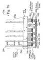
- FIG. 13shows a partial cross-sectional view 56 of an ultra high frequency spring probe substrate 16 .
- a spring probe 61 and related electrical conductors 60 , 68 , 64 on and through the substrate 16are required to be impedance matched
- one or more conductive reference surfaces 58 a, 58 b, 58 c, 58 d and vias 65 a, 65 b, 65 cmay preferably be added, either within or on the substrate 16 .
- the substrate 16may also contain alternating ground reference traces 62 a, 62 b, which are connected to reference planes 58 a, 58 b, 58 c, to effectively provide a shielded coaxial transmission line environment 63 .
- the impedance control surfaces 58 a, 58 b, 58 c, 58 dare not limited to the planar surfaces shown in FIG. 13 .
- An insulating layer 66may be deposited on a portion the probe spring 61 , such as on the fixed region of the probe spring 61 , up to but not enclosing the tip 24 ( FIG. 2 ), as well as on the trace 60 , which connects the spring probe 61 to the via 68 .
- a conductive layer 58 dmay be deposited on top of the insulating layer 66 , to provide a coaxial, controlled low impedance connection. Alternate layers of conductive materials 58 and dielectric materials 66 can preferably be integrated within the substrate 16 , such as for embodiments which require decoupling capacitors in close proximity to a probe spring 61 .
- a thin oxide layer 57may preferably be deposited between the substrate 16 and a conductive reference plane 58 c, thereby forming a high capacitance structure 59 between the spring probe 61 and the ground planes 58 a and 58 b.
- one or more assembled components 69such as passive components 69 (e.g. typically capacitors, resistors, and/or inductors), or active component devices 69 , may be incorporated on either surface 62 a, 62 of the substrate.
- the fixed portions 15 of the spring probes 61typically extend a relatively short distance across the substrate 16 .
- Traces 60 located on the surface of the substrate 16are electrically connected to the fixed portions 15 of the spring probes 61 , and electrically connect the probe springs 61 to the vias 68 .
- the tracesmay be comprised of a different material than the spring probes 61 , and are preferably comprised of metals having high electrical conductivity (e.g. such as copper or gold).
- FIG. 14is a partial plan view 72 of a substrate 16 , in which a plurality of distribution fanout traces 60 are defined on the probe surface 62 a of the substrate 16 , between a plurality of spring probes 61 and a plurality of via contacts 70 .
- the spring probes 61which are preferably photolithographically formed springs 61 , may currently be formed with a pitch of approximately 0.001 inch.
- the traces 60are preferably routed on the probe surface 62 a, to connect to via contact areas 70 , which are preferably laid out in a matrix across the surface of the substrate 16 .
- the via contact areas 70are positioned with a probe surface first distribution pitch 74 a, and a probe surface second distribution pitch 74 b.
- lower standoffs 75are preferably provided on the probe surface 62 a of the substrate 16 , such as to prevent the substrate 16 from damaging a wafer under test 104 , or to set the spring probe tips 24 to operate at an optimal contact angle.
- the lower standoffs 75are preferably made of a relatively soft material, such as polyamide, to avoid damage to the semiconductor wafer under test 104 .
- the standoffs 75are preferably placed, such that when the massively parallel interface assembly 78 is aligned with a device 44 on a semiconductor wafer 104 , the standoffs 75 are aligned with the saw streets 136 ( FIG. 18 , FIG.
- the height of the lower standoffs 75are preferably chosen to limit the maximum compression of the spring probes 61 a - 61 n, thus preventing damage to the spring probes 61 a - 61 n.
- the substrate 16also typically includes one or more alignment marks 77 ( FIG. 14 ), preferably on the probe surface 62 a, such that the probe surface 62 a of the substrate 16 may be precisely aligned with a wafer to be tested 104 .
- FIG. 15is a plan layout view 78 of a chip scale integrated circuit package die region 80 having stress metal springs 84 connected to IC pads 82 and laid out on the upper substrate surface 85 a, before release from the upper substrate surface 85 a.
- the stress metal springs 84each have a spring contact region 86 , which before release are preferably laid out in an IC surface first fanout pitch 87 and an IC surface second fanout pitch 88 .
- FIG. 16is a plan layout view 90 of an integrated circuit die region 80 having stress metal springs 84 connected to IC pads 82 and extending from the substrate surface 85 a, after release from the upper substrate surface 85 a.
- each of the stress metal springs 84extend from respective release regions 18 , whereby the contact regions 86 ( FIG. 15 ) are rotated though an effective spring angle 30 ( FIG. 3 , FIG. 4 ), such that each stress metal spring 84 further preferably defines a spring contact surface 92 .
- each of the spring contact surfaces 92are preferably laid out on a spring contact first fanout pitch 94 and on a spring contact second fanout pitch 96 .
- FIG. 17is a partial cutaway view of an chip scale integrated circuit package 100 having looped stress metal springs 84 connected to IC pads 82 and extending from the substrate spring surface 85 a, wherein a portion of the stress metal springs 84 are embedded within a support substrate 106 comprised of an electrically insulative material.
- the support substrate 106is typically comprised of a polymer substrate which provides support for each of the springs 84 .
- the support substrate 106is a compliant polymer, i.e. an elastomer.
- the support substrate 106provides mechanical protection and adds mechanical support, i.e. strength, to the springs 84 , provides passivation to the integrated circuit die regions 80 , and adds mechanical strength to the assembly.
- the support substrate 106provides mechanical strength for chip attachment to the printed wiring board, and controls the amount of wetting for solder or epoxy on the springs 84 .
- the compliant springs 84provide the compliant connection to manage the thermal expansion mismatch between the die region 80 and a printed wiring board 216 .
- the support substrate 106can alternately be used to provide support for a wide variety of chip scale contacts 84 .
- the support substrate 106adds strength to the springs 84 , and typically improves the robustness of the springs 84 to handling and use, that could otherwise result in breakage.
- the springs 84provide a conductive path between the integrated circuit 102 and the loop spring contact regions 92 , which extend beyond the outer surface of the support substrate 106 .
- FIG. 15 , FIG. 16the springs 84 provide a conductive path between the integrated circuit 102 and the loop spring contact regions 92 , which extend beyond the outer surface of the support substrate 106 .
- the loop spring contact regions 92may preferably have an enhanced contact area geometry, such as to provide dimensional tolerance for electrical connections for testing, burn-in, or for subsequent device operation.
- stress metal springs 84 , 152may preferably also comprise one or more metal or metal alloy coatings 166 . These coatings may be applied using eletro or electroless plating, sputtering, evaporation, or equivalent processes.
- Specific metals or alloys for spring coatingsare selected to provide a high integrity physical mounting between the IC package 100 and its mounting substrate (e.g., printed wiring board 216 ), a low resistance electrical path between IC contact pads 82 and spring contact region 92 , as well as a surface compatible with either a solder or pressure connection to solder ball 220 ( FIG. 54 ) or spring contact region 92 ( FIG. 17 ), respectively.
- Desirable metals for stress metal spring body and tip coatingsinclude nickel or nickel alloys such as, nickel iron, nickel cobalt, nickel cobalt iron, nickel molly, nickel tungsten, nickel iron tungsten, nickel cobalt tungsten, nickel rhodium, nickel cobalt manganese, nickel iron rhodium, nickel iron manganese, and silver, rhodium, palladium or palladium alloys such as palladium cobalt, cobalt, silver, gold or gold alloys, tin and tin alloys, copper and copper alloys, and lead containing and lead free solder materials.
- nickel or nickel alloyssuch as, nickel iron, nickel cobalt, nickel cobalt iron, nickel molly, nickel tungsten, nickel iron tungsten, nickel cobalt tungsten, nickel rhodium, nickel cobalt manganese, nickel iron rhodium, nickel iron manganese, and silver, rhodium, palladium or palladium alloys such as pal
- Metal coatingscan be applied to exemplary stress metal springs 14 a - 14 n in FIG. 2 either before or after release from substrate 16 or to those of springs 84 , 152 either before or after release from the die region 80 .
- Metallic coatingssuch as exemplary coating 166 in FIG. 24 , can also be used to increase the strength of exemplary springs 84 of FIG. 17 or 152 of FIGS. 22-27 to improve the robustness of the springs to handling and use.
- Metallic coating 166can also be used to reduce the overall electrical resistance of exemplary springs 84 , 152 .
- harder metalssuch as rhodium, palladium or a palladium alloy such as palladium cobalt, or other alloys may be used to provide improved contact performance by increasing resistance to mechanical wear and debris pickup from printed circuit board pads.
- These metalsmay be plated as primary, secondary, or subsequent plating metal layers to serve as stress metal spring contact regions, such as in region 92 in FIG. 17 , or other exemplary contact regions including 92 and 158 of FIG. 22,158 and 162 of FIG. 23, 92 and 158 of FIG. 24-27 .
- Exemplary contact bumps 159 in FIGS. 25-27can be filled or plated on the stress metal tips 158 in FIG. 26 either before or after lifting the springs from the substrate.
- the bumpscan be fabricated using selected metals and alloys such as nickel or nickel alloys, rhodium, palladium, or palladium alloys, copper or copper alloys, gold or gold alloys, and solders such as mentioned above.
- Additional plating layers or buttonscan be applied before or after lifting the springs from the substrate and can be selectively applied to the spring tips 92 in FIG. 27 using photolithographic methods.
- the use of a plated metallic coating 166creates a higher contact force between spring 84 and the pad on a circuit board, to reduce the electrical contact resistance.
- a metal plating layer 166such as a nickel alloy, is then followed by subsequent plating layers 166 , such as gold or rhodium, to provide increased spring strength and, lowered spring resistance, as well as improved contact performance.
- stress springs 84 , 152which preferably comprise a plated metal coating 166
- a large portion of the required strength for the springs 84 , 152can be provided by the plating 166 , such that the stress metal layers 17 a - 17 n ( FIG. 13 ) are not required to provide as much strength, such as compared to an unplated spring 84 , 152 . Therefore, in some plated stress spring embodiments, the stress metal layers 17 a - 17 n ( FIG. 13 ) may only be used to define the structural shape before plating, thereby relaxing the process, i.e. metallurgical, parameters needed for the stress metal layers 17 a - 17 n.
- support substrate 106can alternately be comprised of a relatively hard polymer material 106 , such as polyimide or a conventional molding material, such as to create a rigid IC package for direct surface mount applications to printed circuit boards 216 .
- Chip-scale package integrated circuit devices 100 for use in harsh environmentsmay also preferably further comprise plated metal spring coatings 166 combined with a polymer underfill 217 ( FIG. 54 ).
- a boundary layer 161( FIG. 26 , FIG. 46 ) can preferably be used on the stress metal springs 84 , 152 , in which the boundary layer 161 is initially established as the first layer, i.e. the layer in contact with the release region 18 . After release from the substrate surface 85 a, the stress metal springs 84 loop through an effective angle 30 , such that the boundary layer 161 becomes the outer layer of the contact region 92 , for springs 84 , 152 having an effective angle greater than 180 degrees.
- the boundary layer 161is preferably comprised of a highly conductive and non-corrosive metal, such as gold, rhodium, or palladium.
- the boundary layer 161is preferably be patterned on the substrate surface 85 a, such as to be selectively applied to portions of the springs 84 , e.g. such as to control the wetting of solder on a contact area 92 of a spring 84 .
- the stress metal springs 84preferably have a effective angle 30 which is typically larger than 180 degrees, such that the leading edges 155 of the springs 84 preferably extend back into the support substrate 106 , defining a loop spring contact region 92 along the convex arch of the spring 84 .
- the chip scale package semiconductor 100 shown in FIG. 16shows a large effective spring angle 30
- a wide variety of chip scale package contact springs 84can be enhanced by the use of support substrates 106 and one or more plating layers 166 .
- Some springs 84 , 152 which require higher force or which need to contact smaller pads on a printed circuit board 216preferably have an effective angle 30 which is typically less than 90 degrees.
- the chip scale semiconductor package 100can be efficiently fabricated using batch processing methods.
- a release layer 18such as titanium or silicon oxinitride, is typically initially fabricated on the wafer die region 80 .
- one or more metal layers 17 with controlled stresssuch as layers 17 a, 17 b in FIG. 13 , are deposited on top of the release layer 18 .
- the stress metal layers 17are comprised of the same or similar deposited metal, which have an initial stress gradient.
- the stress metal springsare built in compliance to photolithographic springs, such as described above, or as disclosed in U.S. Pat. No. 5,848,685, U.S. Pat. No. 5,613,861, or U.S. Pat. No. 3,842,189, which are incorporated herein by reference.
- the stress metal layers 17are then typically patterned, to form spring and interconnect traces, using conventional photolithography and etch processes.
- a dielectric release windowsuch as polyimide, oxide, or nitride is defined, after the stress metal layers 17 are controllably etched.
- the release windowdefines the areas 18 where the spring metal is released from the substrate surface 58 a, forming springs 84 .
- the springs 84are preferably plated 166 , to adjust the spring constant, or to increase the strength of the stress metal springs 84 .
- the exposed contact portions 92 of the stress metal springs 84are preferably coated with gold or other material, such as for ease of soldering during a subsequent IC circuit assembly process.
- a barrier metal 161can also be formed on the stress metal spring 84 , before stress metal deposition.
- the support substrate layer 106is then typically applied on the wafer 104 , after the springs 84 are released and are preferably plated.
- the support substrate 106typically comprising a polymer, functions as a protective layer for the integrated circuit device.
- the support substrate 106is controllably applied to a desired depth, such that the contact portions 92 of the stress metal springs 84 are exposed.
- the support substrate 106is subsequently etched back, to expose the top contact region 92 of the springs 84 .
- a photomaskis preferably used for an etched support substrate 106 , to controllably define the precise location and shape of the exposed region of the contact portions 92 of the stress metal springs 84 .
- the chip scale integrated circuit package 100simplifies the process and reduces the number of processing steps in the fabrication of chip scale packages.
- a chip scale integrated circuit package 100can be easily fabricated through batch processing techniques, similar to batch process manufacturing methods for semiconductor assemblies, such as integrated circuit devices.
- the chip scale integrated circuit package 100thus eliminates the serial process of bonding device leads to an integrated circuit one at a time. As well, the chip scale integrated circuit package 100 enables tight pitch packages with high electrical performance.
- chip scale integrated circuit packages 100can also provide a direct temporary contact to a board, such as to a printed circuit board 216 , by pressure, which can eliminate the need for a socket or interposer connection.
- This temporary contactcan also function as a probe contact, thus allowing the probe contact to be reduced to a simple pad array on a printed circuit board 216 .
- FIG. 18is a side view 110 of integrated circuit die regions 80 on a semiconductor wafer 104 .
- Each of the integrated circuit die regions 80have contacts 47 , such as contact pads or stress metal springs 84 .
- Saw streets 114are defined between the integrated circuit die regions 80 .
- the integrated circuit die regions 80are chip scale semiconductor packages 100 , having stress metal spring contacts 84 and a support substrate 106 , as described above.
- FIG. 19is a side view 112 of a semiconductor wafer 104 , having integrated circuit die regions 80 , in which the wafer 104 is adhesively mounted to a compliant wafer carrier substrate 115 .
- the compliant substrate 115has a first surface 116 a and a second surface opposite the first surface 116 b.
- the first surface 116 aincludes an adhesive layer, such that a wafer 104 may readily be mounted for subsequent IC separation and processing.
- a support 118is also typically attached to the compliant substrate 115 .
- FIG. 20is a side view 120 which shows of the separation 122 of integrated circuits on a semiconductor wafer 104 , which is mounted to a compliant carrier substrate 115 .
- a sawis typically used to form separations 122 between integrated circuits 44 and die regions 80 , along the saw streets 114 .
- the compliant wafer carrier 115is typically comprised of a compliant polymer material, such as RISTONTM, Part Number 1004R-9.0, from Nitto-Danko, Japan, or Ultron Systems, of Moore Park, Calif. As described below, some preferred embodiments of the compliant wafer carrier 115 are thermally conductive and/or electrically conductive.
- RISTONTMPart Number 1004R-9.0
- FIG. 21is a side view 130 which shows separated integrated circuits 44 , 100 on a compliant wafer carrier 115 .
- the compliant wafer carrier 115holds the integrated circuit dice 44 , 100 together in position after wafer separation 122 , e.g. such as after saw and break, making it possible to handle all the separated dice 44 , 100 from a wafer 104 as a group, through back end assembly, test and burn in.
- a compliant wafer carrier 115integrates assembly and wafer level testing and burn-in processes, and offers the speed advantage of parallel testing and simplicity in handling.
- the integrated circuit dice 44are sometimes burned-in and tested before packaging and singulation from the wafer.
- a common difficulty encountered in a conventional wafer-level pre-singulation approachis the complexity in managing the thermal expansion mismatch between the silicon wafer and the connector systems, which are required to make connections between the integrated circuit dies on the wafer and the system electronics.
- defects induced by the packaging, singulation, and handlingare not screened out by such a process.
- a stress metal spring chip scale package 100in conjunction with a compliant carrier 115 , as described above, allows the use of low cost printed wiring board material 282 , whose material coefficient of expansion can be different from the carrier mounted devices under test 100 , to contact the dice during test and burn-in.
- various embodiments of a massively parallel interface assembly 278e.g. such as massively parallel interface assembly 278 a shown in FIG. 55 , allow connection to a wide variety of carrier-mounted integrated circuits 44 , 100 .
- chip scale package 100 and/or a massively parallel interface assembly 278allow the test and burn of integrated circuit dice 44 , 100 after packaging and singulation 122 , making it possible to detect assembly, saw and handling caused defects, while keeping the die in position for precision handling with massive parallelism.
- the semiconductor wafer 104having stress metal springs 84 which are processed onto the active surface 85 a and are preferably partially encapsulated 106 , is attached to a compliant decal wafer carrier 115 .
- the carrier 115is similar to a conventional “blue” tape carrier which is commonly used for wafer sawing in the semiconductor processing industry.
- a contact fixture 132such as the massively parallel test assembly 278 ( FIG. 55 , FIG. 57 , FIG. 68 , FIG. 70 , FIG. 71 ), typically including a printed wiring board 282 , comprises connections and associated electronics for connecting to and for testing the integrated circuits 44 , 100 .
- the contact fixture 132 connectionsare designed to match the connections 47 , such as spring leads 84 , on the devices under test 44 , 100 , when the contact fixture 132 is pressed onto the DUT devices 44 , 100 on the compliant carrier 115 .
- a pressure plate support 134preferably constructed of a material having a similar thermal coefficient of expansion (TCE) to the TCE of the printed wiring board 282 , supports the back surface 116 b of the compliant carrier 115 .
- TCEthermal coefficient of expansion
- the IC contact fixture 132is fixedly attached 136 in relation to the pressure plate support 134 , forming a sandwich structure 130 , in which the mounted integrated circuit die 44 , 100 and the compliant carrier 115 are held in place.
- the pressure plate support 134may also be preferably comprised of a compliant material, whereby the pressure plate support 134 and the carrier-mounted die 44 , 100 can readily conform to the system board 282 .
- the printed wiring board 282When the temperature of this sandwich structure 130 is raised to the test and burn-in temperature, the printed wiring board 282 , having a higher coefficient of expansion than the silicon die regions 80 , expands faster than the silicon die regions 80 .
- friction between the integrated circuit die 44 , 100 and the printed wiring board 282 and the pressure plate support 134acts to drag the integrated circuit die 44 , 100 , along with the printed wiring board 282 , since the integrated circuit die 44 , 100 are separated 122 from each other, and are only connected through the compliant flexible carrier 115 . Therefore, the relatively independent movement of each of the separated integrated circuit die 44 , 100 maintains pad to lead alignment between the integrated circuits 44 , 100 and the printed wiring board 282 .
- the separated integrated circuit die 44 , 100which are mounted to the compliant carrier 115 , are able to move relative to each other, while holding their positions on the compliant carrier 115 . Therefore, the separated integrated circuit die 44 , 100 can be handled and processed as a “wafer” assembly, while maintaining sufficient connections to the IC contact fixture 132 .
- the printed wiring board 282 and the pressure plate support 134are not required to be comprised of a material having a similar coefficient of expansion TCE to the IC substrate 104 .
- the compliant carrier-mounted dice 44 , 100are able to move with the system board 282 and the support structure 134 , such that the dice 44 , 100 remain in electrical contact with the system board 282 within the IC contact fixture 132 . Furthermore, since the dice 44 , 100 are tested after packaging and singulation, the burn in and test applied to the dice will detect assembly induced defects in the dice 44 , 100 .
- a temperature controller 144is preferably attached to the sandwich structure 130 , such as to provide heating or cooling during testing and/or burn-in processes.
- the carrier 115is comprised of a thermally conductive material, which functions as a thermal control plane during testing or burn-in, wherein the back side of the integrated circuits are in thermal contact to temperature control 144 , such as for cooling and/or heating, through the compliant tape layer 115 .
- the carrier 115may preferably be comprised of electrically conductive material, whereby the carrier 115 may provide an electrical connection 140 to the back surface of the separated and mounted integrated circuit dice 80 .
- FIG. 22is a partial cross-sectional view 150 of a stress metal spring interposer 151 a, comprising one or more springs 152 which extend from a first surface 156 a to a second surface of an interposer substrate 154 .
- the springs 152also typically comprise contact pads 158 which extend from the first surface of the interposer substrate 154 .
- Stress metal spring interposers 151provide ultra-high density, compliant through connections, and provide high density connections over extreme temperature ranges.
- Stress metal spring interposers 151use thin film stress metal to form a tight array of thin film springs, held together by a substrate 154 comprises of a polymer material. Electrical connections are made from one side 156 a of the polymer sheet to the other side 156 b by the conductive springs 152 .
- a high density connection between the two surfaces 156 a, 156 bcan therefore be made by having each of the surfaces pressing against one side of the polymer sheet with stress springs embedded.
- Different tip shapescan be engineered on each end of the spring 152 , such as for different contact materials.
- the stress metal spring interposers 151are built in accordance to U.S. Pat. No. 3,842,189 and/or U.S. Pat. No. 3,842,189, which are incorporated herein by reference.
- FIG. 23is a side cross-sectional view 160 of a stress metal spring interposer 151 b having formed bumps 162 on the second surface contact region 158 .
- FIG. 24is a side cross-sectional view 64 of a plated stress metal spring interposer 151 c.
- the springs 152as well as stress springs 84 , are preferably comprised of layers of metal having 17 ( FIG. 13 ) having different initial levels of stress, such that the springs form an effective spring angle 30 ( FIG. 3 ) during fabrication.
- FIG. 25is a side cross-sectional view of a stress metal spring interposer 151 d having filled bumps 159 on a first surface contact region, and looped stress metal springs 152 which partially extend beyond a polymer interposer layer 154 , defining a hollow contact region 157 between the contact area 92 of the looped stress metal springs and the top surface 156 b of the polymer layer 154 .
- FIG. 26is a side cross-sectional view of a stress metal spring interposer 151 e, in which the interposer layer comprises a plurality of polymer layers 154 a, 154 b.
- the looped stress metal springsfurther comprise a boundary layer 161 .
- the boundary layer 161comprises a metal having high electrical conductivity and/or corrosion resistance. The boundary layer 161 may also be used for increased stress spring strength.
- FIG. 27is a side cross-sectional view of a stress metal spring interposer 151 f, in which the stress metal springs 152 have an effective spring angle less than 90 degrees, and in which the interposer substrate 154 adds strength and/or protection for the stress metal springs 152 .
- Loop stress metal prings 152such as used for the stress metal chip scale package 100 , the stress metal interposer 151 , or for the stress metal contactor 196 , such as contactor 196 a in FIG. 41 , can have a wide variety of leading edge and contact area geometries.
- FIG. 28is a partial view of a square leading end 155 a of a looped stress metal spring 84 , 152 .
- FIG. 29is a partial view of a pointed leading end 155 b of a looped stress metal spring 84 , 152 .
- FIG. 30is a partial view of a pointed leading end 155 c of a looped stress metal spring 84 , 152 , which further comprises retaining grooves 157 .
- FIG. 31is a partial view of a pointed leading end 155 d of a looped stress metal spring 84 , 152 , which further comprises retaining ledges 163 .
- the leading end 155 of high effective angle looped stress metal springs 84 , 152can have a variety of leading end geometries 155 , since the leading ends 155 are typically not used for contacting.
- the desired geometry of the leading end 155is typically chosen to control the formation of the non-planar springs 152 , during lift-off from a substrate, i.e. the spring tip geometry helps the stress metal spring 152 to lift in the correct direction.
- the geometry of the leading end 155is chosen to anchor the loop spring probe within a supporting substrate 154 , such as with grooves 157 or ledges 163 .
- FIG. 32is a plan view of a contact area of a looped stress metal spring 152 , in which the contact area 92 which extends beyond the outer surface 156 b of the polymer layer 106 , 154 comprises an expanded rectangular contact region 92 a.
- FIG. 33is a plan view of a contact area 92 b of a looped stress metal spring 152 , in which the contact area 92 b which extends beyond the outer surface 156 b of the polymer layer 106 , 154 comprises an expanded octagonal contact region 92 b.
- FIG. 32is a plan view of a contact area of a looped stress metal spring 152 , in which the contact area 92 which extends beyond the outer surface 156 b of the polymer layer 106 , 154 comprises an expanded octagonal contact region 92 b.
- the contact area 92 ccomprises an expanded diamond-shaped contact region 92 c.
- the stress metal springs 84 , 152are typically comprised of photolithographically formed layers 17 , e.g. such as 17 a, 17 b in FIG. 13
- the defined contact area 92can have a variety of geometries, such as to provide dimensional tolerance for the interconnection structure.
- FIG. 35is view of a first step 170 of a stress metal spring interposer construction process, in which a sacrificial substrate 172 is provided.
- the sacrificial substrate 172includes a pad formation structure 174 .
- the sacrificial substrate 172can be fabricated from a wide variety of etchable materials, such aluminum or silicon. As described below, the sacrificial substrate 172 is used as a temporary substrate in the fabrication of a spring interposer 151 , and is eventually removed, typically by an etching process.
- FIG. 36is a view of a second step 176 of a stress metal spring interposer construction process, in which one or more stress metal spring layers 178 , such as stress metal layers 17 , are established on the sacrificial substrate 172 , and in which spring release regions 18 are controllably defined.
- the stress metal spring interposer 151in which the springs 152 include contact pads 158 , the successive layers 17 of the spring 152 are formed directly into pad formation structures 174 .
- discrete contact pads 159FIG. 26 , FIG. 27
- are formed within pad formation structures 174such as by a fill and polish process, in which the successive layers 17 of the spring 152 are formed over the discrete contact pads 158 .
- FIG. 37is a view of a third step 180 of a stress metal spring interposer construction process, in which non-planar portions of the stress metal springs 152 extending from the sacrificial substrate 172 are controllably formed, upon release from the release regions 18 .
- the inherent stress of the metal layers 17forms a spring having an effective spring angle 30 .
- the effective spring angleis greater than 180 degrees, e.g. such as 270 degrees, such that the spring 152 has a convex contact surface 92 ( FIG. 39 ).
- spring shapes and liftcan be used, including springs 152 with sharp contact tips 24 , which point towards the contact pad surface at various angles 30 .
- the springs 152provide ultra high-density connectivity between the two different surfaces, while maintaining compliance.
- Different contact shapescan be fabricated on the contact surfaces, by first defining the desired contact shapes on the substrate material 172 .
- the stress metal springs 152 shown in FIG. 37also preferably comprise a plating layer 166 ( FIG. 24 ), which is typically applied to the formed non-planar springs 152 , before the formation of the support substrate 154 , such as an elastomer 154 , such that the plating 166 is applied to the non-planar portions of the stress metal springs 152 .
- Plating 166can be used for spring strengthening, enhanced conductivity, and/or for corrosion protection.
- FIG. 38is a view of a fourth step 182 of a stress metal spring interposer construction process, in which an interposer substrate 184 is applied on the sacrificial substrate 172 and typically over the stress metal springs 152 .
- FIG. 39is a view of a fifth step 186 of a stress metal spring interposer construction process, in which an outer portion of the applied interposer substrate 184 is removed 188 to form a contoured interposer substrate 154 , such as by etching, to access upper contact portions 92 of the stress metal springs 152 .
- FIG. 40is a view of a sixth step 190 of a stress metal spring interposer construction process, in which the sacrificial substrate 172 is removed 192 , such as by etching from the interposer substrate 154 , exposing the lower contact portions 158 of the stress metal springs 152 .
- the spring interposer 151can be configured for a wide variety of applications, and can be used to provide a high density interface, e.g. such as 50-100 microns.
- the spring interposer 151can be fabricated to have a variety of contact area geometries 92 as well, such as a square, rectangle, or circular configurations, based on the desired application.
- some embodiments of the spring interposer 151have an effective spring angle 30 less than 180 degrees, whereby the springs include a contact tip 24 to establish electrical connections.
- some embodiments of the spring interposer 151preferably have a planar lower contact region 158 .
- a boundary layer 161such as a metal having enhanced conductivity, corrosion resistance, or solderability characteristics (e.g. such as gold, rhodium, or palladium), may also preferably be established as the lowest layer of stress metal layers, such that the boundary layer 161 provides the contact surface 92 .
- the interposer substrate 154 , 184comprises a plurality of interposer layers 154 a, 154 b ( FIG. 26 ).
- a first thin layer 154 acomprising a relatively rigid electrically insulative material, such as polyimide, provides increased dimensional control, handleability, and mountability for the interposer 151
- the second interposer layer 154 btypically comprising a relatively non-rigid electrically insulative elastomer, provides enhanced support and compliance for the springs 152 .
- the thin semi-rigid layer 154 amay also preferably comprise one or more openings.
- FIG. 41is a side cross-sectional view 194 of a stress metal spring contactor 196 a having contact areas 92 extending from an elastomeric support substrate 154 , which are electrically connected to vias 200 that extend through a wafer substrate 198 .
- FIG. 42is a side cross-sectional view of a stress metal spring contactor 196 b having bumped contact areas 162 extending from a support substrate 154 .
- FIG. 43is a side cross-sectional view of a plated stress metal spring contactor 196 c having plated contact areas 92 extending from a support substrate 154 .
- FIG. 44is a side cross-sectional view of a plated stress metal spring contactor 196 d having contact areas 92 extending from the contactor substrate 198 .
- FIG. 45is a side cross-sectional view of a stress metal spring contactor 196 e having looped stress metal springs 152 which partially extend beyond a polymer layer, defining hollow regions 157 between the contact area 92 of the stress metal springs 152 and the upper surface 156 b of the support substrate 154 .
- FIG. 46is a side cross-sectional view of a stress metal spring contactor 196 f in which the support layer comprises a plurality of polymer layers 154 a, 154 b.
- a stress metal spring contactor 196 gin which the stress metal springs 152 further comprise a boundary layer 161 , such as gold, rhodium, or palladium, and have an effective spring angle 30 less than 90 degrees.
- the stress metal spring contactor 196 spring structurecan be used for probing solder balls 220 on a bumped wafer, such as to provide a temporary contact to solder bumps on flip chip devices.
- the stress metal spring contactor 196can be fabricated using batch processing methods, which decreases the cost of the contactor, and provides a short turnaround time.
- FIG. 48is a view of a first step 202 of a stress metal spring contactor construction process, in which a spring probe contactor substrate 198 having vias 200 is provided.
- FIG. 49is a view of a second step 204 of a stress metal spring contactor construction process, in which in which one or more stress metal springs 178 are established on the spring probe contactor substrate 198 , wherein each of the springs 178 comprise a plurality of layers 17 having different levels of inherent stress.
- FIG. 50is a view of a third step 206 of a stress metal spring contactor construction process, in which in which non-planar portions 152 of the stress metal layers extending from the contactor substrate are controllably formed.
- FIG. 51is a view of a fourth step 208 of a stress metal spring contactor construction process, in which the formed non-planar portions of the probe springs 152 extending from the contactor substrate are preferably plated 166 .
- the plating layer 166is typically applied to the formed springs 152 , before the formation of an elastomer support layer 154 , 184 , such that the plating 166 is applied to the non-planar portions of the stress metal 152 .
- Plating 166is preferably used for contactor embodiments which require spring strengthening, enhanced conductivity, and/or corrosion protection.
- FIG. 52is a view of a fifth step 210 of a stress metal spring contactor construction process, in which a secondary substrate 184 is established over the formed non-planar portions of the probe springs 152 extending from the contactor 198 .
- FIG. 53is a view of a sixth step 212 of a stress metal spring contactor construction process, in which an outer portion of the applied secondary substrate 184 is removed 214 to established a contoured substrate 154 , to access upper contact portions 92 of the stress metal springs 152 .
- FIG. 54is a side cross-sectional view 214 of a probe spring contactor 196 having a spring probe contact area 92 extending from the support substrate 154 , in which a connection is established between the compliant stress metal spring contactor lead 152 and a printed wiring board (PWB) 216 , though a solder ball contact 220 and a board contact 218 .
- PWBprinted wiring board
- FIG. 55is a partial expanded cross-sectional view of a massively parallel test assembly 278 a having an intermediate system board 282 for connection to separated integrated circuit devices 44 , 100 on a compliant carrier 115 .
- FIG. 56is a partial perspective view 310 of a massively parallel interface assembly 278 a.
- FIG. 57is a partial expanded cross-sectional view 320 of a massively parallel test assembly 278 a having an intermediate system board 282 , which shows staged pitch and distribution across a system board 282 , and a flex circuit 290 having a pad matrix 288 ( FIG. 55 ) of electrical connectors 319 a - 319 n.
- the interface assembly 278 ais positioned in relation to a compliant wafer carrier 115 , having one or more integrated circuits 44 , which are separated by IC separation 122 ( FIG. 20 , FIG. 21 ).
- the test structures shown in FIG. 21 and FIG. 55allow parallel testing and burn-in for separated integrated circuit devices 44 , 100 which are mounted on a compliant carrier 115 .
- the chip scale packaged devices 44 , 100are loosely held together by the compliant carrier 115 , and make contact to the system transformer board 282 . These devices can be connected as shown to a standard tester, or through a set of electronics, to minimize the number of connections between the separated integrated circuit devices 44 , 100 and the tester.
- the massively parallel interface assembly 278 aprovides electrical interconnections to each of the integrated circuit devices 44 , 100 located on the compliant carrier 115 , to work effectively in a typical integrated circuit testing environment.
- the interface assembly 278 ais readily used for applications requiring very high pin counts, for tight pitches, or for high frequencies.
- the interface assembly 278 ais easily adapted to provide electrical contact for all traces 46 ( FIG. 7 ) and input and output pads 47 ( FIG. 7 , FIG. 9 ) for one or more integrated circuit devices under test 44 on the compliant carrier 115 .
- the conductive pads 284 a - 284 n on the lower surface of the system board 282are typically arranged with a pad pitch 324 ( FIG. 57 ), such that the conductive pads 284 a 284 n are aligned with the electrical contacts 47 , such as the contact regions 92 of stress metal springs 84 , on the carrier-mounted integrated circuit devices 44 , 100 .
- the conductive pads 284 a - 284 n on the lower surface of the system board 282are then routed to conductive paths 286 a - 286 n, which are typically arranged with a system board pitch 326 .
- the electrically conductive connections 328 a - 328 nwhich may be arranged within one or more connection regions 332 , are located on the upper surface of the system board 282 , and are routed to the conductive paths 286 a - 286 n.
- the electrically conductive connections 328 a - 328 nare typically arranged within the connection region 332 , with a system board pad matrix pitch 320 , which is typically aligned with the flex circuit pad matrix pitch 334 for each of the test electronics modules 292 a - 292 k ( FIG. 55 ).
- the system board matrix pitch 320is typically chosen such that the electrically conductive connections 328 a - 328 n are aligned with the flex circuit electrical connectors 319 a - 319 n located on the flex circuits 290 , which are typically arranged in a plurality of pad matrices 288 ( FIG. 56 ), having a flex circuit pad matrix pitch 334 .
- the test electronics modules 292 a - 292 kare a basic building block for most of the embodiments of the massively parallel interface test assemblies 278 a - 278 d.
- the test electronics modules 292 a - 292 kare mounted in parallel (e.g. as seen in FIG. 55 ), to form an array of modules 292 a - 292 k, which each provide electronics support to one or more columns 339 ( FIG. 58 , FIG. 59 ) of integrated circuit devices 44 , 100 on a compliant carrier 115 or in a wafer form 104 , or to a portion of a column 339 or die 44 , along which the test electronics modules 292 a - 292 k are mounted.
- FIG. 56is a partial perspective view 310 of a massively parallel interface assembly 278 a, wherein test electronics modules 292 are mounted on a frame 302 .
- Each of the test electronics modules 292 shownincludes a preferred flex circuit 290 , having a pad matrix 288 of electrical contactors 319 , and one or more power control modules 300 .
- the flex circuit 290 for each of the test electronics modules 292is mounted on one or more buss bars 298 a - 298 h, and extends downwardly through the frame 302 .
- the buss bars 298 a - 298 hare attached to the frame 302 , such as by electrically isolated fasteners 312 , thereby providing a substantially rigid structure.
- the frame 302preferably includes test module alignment guides 318 , as well as frame to system alignment pins 314 and means 316 for fastening the frame 302 to a wafer chuck 306 ( FIG. 55 ) or to a pressure plate support 134 ( FIG. 21 ).
- the assembly 310may also preferably include other means for holding the test electronics modules 292 a - 292 k, such as a card cage (not shown) located below the frame 302 .
- the separated carrier-mounted integrated circuit devices 44 , 100interface to a system board 282 , which provides a standard interface to the tester electronics, at a coarser pitch than the contact pitch of the integrated circuit devices 44 , 100 .
- the system board 282can be comprised a wide variety of materials, such as ceramic, high density printed wiring board, silicon, glass, or glass epoxy.
- Each of the tester electronics modules 292 a - 292 nare attached to the system board 282 , via a membrane or flex circuit 290 .
- Contacts 319 , 328 between test electronics modules 292 a - 292 k and the system board 282are achieved using solder, pressure contact, or spring probes.
- the spring probesmay have a variety of tip geometries, such as single point springs 14 , interleaved springs 34 , or shoulder point springs 50 , and are typically fabricated using thin-film or MEMS processing methods, to achieve low manufacturing cost, well controlled uniformity, very fine pad pitches 20 , and large pin counts.
- the connections 319 , 328are built in compliance to photolithographic springs, such as described above, or as disclosed in either U.S. Pat. No. 5,848,685 or U.S. Pat. No. 5,613,861, which are incorporated herein by reference.
- the configuration shown in FIG. 55brings power through the switchable power modules 300 , and input/output signal traces 348 ( FIG. 62 , FIG. 63 ) from the pin electronics card 294 to the system board 282 .
- This configurationhas the advantage of reducing routing congestion in the flex circuit or membrane 290 .
- the structure of the interface assembly 278 aprovides very short electrical distances between the carrier-mounted integrated circuit devices 44 , 100 and the controlled impedance environment in the system board 282 , which allows the interface assembly 278 a to be used for high frequency applications.
- FIG. 58is an expanded layer plan view of a integrated circuit dies 44 on a wafer 104 , a circular substrate 16 , and a rectangular system board 282 , wherein the intermediate substrate 16 is typically used in test system embodiments wherein an interface assembly 278 is required to be connected to an entire wafer 104 , i.e. for integrated circuits which are not separated and mounted to a compliant carrier 115 .
- substrates 16which are preferably comprised of silicon (which may be preferably chosen to match the thermal coefficient of expansion (TCE) of a integrated circuit dies 44 under test), the silicon substrate 16 may preferably be fabricated by a similar process to that of a wafer 104 , such that the substrate 16 may be fabricated from a circular wafer substrate 16 .
- devices 44are formed on a wafer 104 , and are typically populated across the wafer 104 by a series of rows 337 and columns 339 , wherein saw streets 114 are located between the rows 337 and columns 339 .
- the silicon substrate 16may preferably be fabricated from one or more rectangular ceramic substrates 16 .
- the substrate 16may include a travel limit mechanism, such as one or more upper standoffs located on the connector surface of the substrate 16 , such as to limit perpendicular travel of the substrate in relation to the system board 282 .
- FIG. 59is an expanded layer plan view of separated integrated circuit dies 44 , 100 on a compliant carrier 115 , which can be directly connected to a system board 282 .
- the carrier-mounted separated integrated circuit dies 44 , 100are typically mounted between the system board 282 and a pressure plate support 134 ( FIG. 21 ).
- the electrically conductive connections 328 a - 328 nwhich are located on the upper surface of the system board 282 , are typically arranged within one or more connection regions 332 , to connect to flex circuit contactors 319 ( FIG. 57 ), which are preferably arranged within a similar number of one or more pad matrices 288 ( FIG. 56 ).
- each of the test electronics modules 292(e.g. 292 a ) is identical to the other test electronics modules (e.g. 292 b - 292 k ), thereby having an identical number of test componentry (thereby having an identical test capacity).
- a similar number of devices 44is routed to each test electronics modules 292 a - 292 k.
- a different number of devices 44may routed to a test electronics module 292 (e.g. 292 a ), such as for outer columns 339 of devices under test 44 on a wafer carrier 115 .
- a test electronics module 292which has a greater capacity than the number of devices 44 which are connected may still be used, typically through programming the test electronics module 292 to bypass testing for unused test circuitry 294 , or through system control 430 ( FIG. 75 ).
- FIG. 60is a partial cross-sectional view of one embodiment of the flexible circuit structure 342 a, having a polyamide layer 344 a, and opposing conductive layers 346 a and 346 b.
- FIG. 61is a partial cross-sectional view of an alternate embodiment of the flexible circuit 290 , which comprises a dielectric flex circuit membrane structure 342 b, and opposing conductive layers 346 a and 346 b.
- the flex circuit membrane structure 342is inherently flexible.
- the flex circuit structure 342is rigid in regions where one or both conductive layers are substantially located. The controlled removal of the conductive layers 346 a, 346 b produces controlled flexibility for the flex circuit 290 , while providing regions of formed conductive paths.
- FIG. 62is a partial perspective view of a flexible membrane circuit structure, wherein a flexible region 290 a is defined on the test card structure 294 a.
- FIG. 63is a partial perspective view of an alternate flexible circuit structure, wherein a flexible circuit 390 b is attached to a test card structure 294 b by attachments 350 (e.g. such as but not limited to fasteners, heat staking, microwelding, or adhesives).
- attachments 350e.g. such as but not limited to fasteners, heat staking, microwelding, or adhesives.
- the test electronics 294 a, 294 b populated on each of the test electronics modules 292 a - 292 kprovide stimulus and response detection for one or more devices under test 44 .
- the test electronics 294 a, 294 bare built on a high density interconnect (HDI) substrate 342 a, 342 b, or on a standard printed wiring board 294 a, which is connected to the flexible circuit 290 .
- the test electronic card 294 a, 94 bis populated with control and response electronics (e.g. such as test electronics 440 in FIG. 75 ).
- Each test electronics module 292(e.g. 292 a ) is connected to the backend electronics and computer interface links 296 (e.g. typically by parallel or serial links).
- the signal pins in the tester electronics modules 292 a - 292 kcan be connected serially, on a daisy chain, to simplify the electrical connections, such as to external test hardware.
- Test vector and setup informationis sent to the pin electronics, from a system computer and control electronics (e.g. such as external pattern generator 446 in FIG. 75 ), through the links 296 .
- test electronics card 294is connected to the flex circuit/membrane 290 .
- Test electronics cards 294may preferably be fabricated as an integral structure with the flexible circuit 290 , such as on an etched thin film substrate, whereby portions of the substrate are etched, to create the flexible membrane circuit 290 .
- a separate test electronics card substrate 294is connected to a flex circuit, typically by solder, wire bond or connectors.
- FIG. 64is a partial cross-sectional view of one embodiment of the flex circuit region 290 of a test electronic module 292 , which preferably includes a thermally conductive pathway 354 across a flex circuit 290 between a power control module 300 and one or more buss bars 298 .
- Each of the buss bars 298 a - 298 hwhich are typically separately electrically connected to a plurality of external power supplies 434 a - 434 h ( FIG. 75 ), are typically electrically isolated from each other by insulators 352 .
- the insulators 352may be a separate layer from the buss bars 298 a - 298 h, or may alternately be an electrically insulative layer 352 on the buss bars 298 a - 298 h.
- FIG. 65is a partial cross-sectional view of an alternate embodiment of the flex circuit region 290 of a test electronic module 292 , in which one or more power control modules 300 a - 300 h are mounted on the inner surface of the flex circuit 290 , and are positioned in thermal contact with a plurality of buss bars 298 a - 298 h.
- FIG. 66is a partial cross-sectional view of a second alternate embodiment of the flex circuit region 290 of a test electronic module 292 , in which a power control module 300 is electrically connected to the outer surface of a flex circuit 300 .
- a power control access region 356is preferably defined through the flex circuit region 290 , whereby the power control module 300 positioned in intimate thermal contact with a buss bar 298 (e.g. such as buss bar 298 b ).
- Power control modules 300typically comprising decoupling capacitors, switching control circuits and regulators for each device under test 44 , are preferably mounted on the flex circuit 290 , as shown in FIG. 64 , FIG. 65 , or FIG. 66 .
- FIG. 67is a perspective view of one alternate embodiment of a test electronics module 292 , in which an integrated module base 357 provides a pad matrix 288 of electrical contacts 319 on a pad matrix planar region 358 .
- One or more power control modules 300are electrically connected to electrical contacts 319 located on the pad matrix 288 , through power control module (PCM) traces 349 , and to one or more buss bars 298 a - 298 h.
- PCMpower control module
- the power control modules 300are also preferably positioned in thermal contact with one or more buss bars 298 a - 298 h.
- Signal traces 348( FIG. 62 , FIG. 63 ) are also connected to electrical contacts 319 located the pad matrix 288 .
- the signal traces 348extend across a link and component planar region 359 , and are either connected to test electronics 294 , or extend to link 296 .
- one or more bus bars 298provide the power and heat sink paths for the power control modules 300 .
- Power for devices under test 44is typically provided through separate rail buss bars 298 , or may alternately share the same rail buss bars 298 with the power control modules 300 .
- the power rail buss bars 298also preferably provide mechanical support for the flex circuit 290 and the system board 282 and/or the test electronics cards 294 a - 294 k.
- the power control module circuits 300are connected in the serial scan path, to provide individual power and ground control to the devices under test 44 .
- FIG. 68is a partial cutaway assembly view of an alternate massively parallel test assembly 278 b having an intermediate system board 282 , in which flexible spring probes 360 are located on the lower surface 339 a ( FIG. 57 ) of the system board 282 .
- the structure and features of the massively parallel test assembly 278 bare otherwise identical to the massively parallel test assembly 278 a shown in FIG. 55 .
- the system board spring probes 360can be used to provide planarity compliance between the system board 282 and the carrier-mounted integrated circuit devices 44 , 100 , and provide high quality electrical connections, over a wide range of temperatures.
- FIG. 69is a partial cross-sectional view of an alternate interface assembly 278 c, wherein a large grid array (LGA) interposer connector 362 is located between a substrate 16 and the system board 282 .
- the LGA interposer connector 362provides a plurality of conductors 164 a - 164 n between the electrical connections 64 a - 64 n on the substrate 16 and plurality of conductive pads 284 a - 284 n on the lower surface of the system board 282 .
- the LGA interposer connector 362is an AMPIFLEXTM connector, manufactured by AMP, Inc., of Harrisburg Pa.
- the interposer connector 362is a GOREMATETM connector, manufactured by W. L.
- a pogo pin interposer 362is used to connect opposing conductive pads 284 a - 284 n on the system board 282 to electrical connections 64 a - 64 n on the substrate 16 .
- FIG. 70is a partial cutaway assembly view of a basic massively parallel test assembly 278 d, in which a substrate 16 has spring probes 61 a - 61 n on a lower probe surface 62 a, and vias 68 a - 68 n which are connected between the spring probes 61 a - 61 n and conductors 64 a - 64 n located on an upper surface 62 b of the substrate 16 , wherein the substrate 16 is directly connected to the test electronics modules 292 a - 292 k.
- FIG. 71is a partial expanded cross-sectional view 366 of the basic massively parallel test assembly 278 d, which shows staged pitch and distribution across a substrate 16 and a test electronics module 292 having a pad matrix 288 of electrical contactors 319 .
- FIG. 72is a partial cross sectional view 370 of an alternate massively parallel interface assembly 378 e, which shows one embodiment of a basic clamping structure 372 .
- the interface assembly 378 eis typically intended for burn-in testing only, whereby test electronics 294 are packaged in small modules 374 .
- the modules 374are mounted directly onto the system board 282 , and are preferably used for burn-in testing, which typically requires significantly less test electronics than the test electronics modules 292 a - 292 k (e.g. such as shown in FIG. 55 ).
- the clamping structure 372 shown in FIG. 72may also be used for the wafer level massively parallel interface assemblies 278 .
- the interposer substrate 16is preferably fabricated from a thin substrate 16 , such as a 10 mil thick glass plate, whereby the substrate 16 may flex slightly, to conform to the surface of integrated circuit dies 44 on a wafer 104 , to accommodate for non-planarity or bowing between the wafer and the interposer substrate 16 .
- a seal 380 around the periphery of the interposer substrate 16preferably provides an air-tight chamber 382 .
- Air pressureis preferably applied between the system board 282 and the interposer substrate 16 .
- An applied pressure 384also thermally isolates the integrated circuit dies 44 on a wafer 104 from the test electronics 374 , 294 . While integrated circuit dies 44 are typically required to operate at elevated temperatures during burn-in testing (e.g. such as at 125-160 degrees Celsius), the test electronics 294 should preferably operate at a lower temperature (e.g. such as below 75 degrees Celsius).
- the wafer chuck 306such as wafer chuck 306 b in FIG. 72 , preferably includes a wafer thermal control system 392 , which preferably comprises a wafer heating system 394 and/or a wafer cooling system 396 , such as to provide temperature control to the wafer under test 104 .
- the wafer thermal control system 392is preferably controlled by a test system temperature controller 388 , which is typically linked 389 to the system controller 432 ( FIG. 75 ).
- the test electronics 374 , 294are preferably located in one or more cooling chambers 376 .
- a cooling system 390is preferably used to control the operating temperature of the test electronics 374 , 294 within the cooling chambers 376 , and is also preferably controlled by the test system temperature controller 388 .
- a wafer loading vacuum circuit 386having vacuum tracks 408 ( FIG. 73 ), is preferably built into the wafer chuck 306 , to provide vacuum suction to hold the wafer 104 in position, and to improve planarity between the substrate connector 16 and the wafer 104 .
- Test System ArchitectureThe test system consists of an alignment set up, which performs wafer alignment, cooling unit, and tester electronics.
- the alignment subsystem and cooling unitscan be built with technology known in the art.
- FIG. 73is a first partial expanded cross-sectional view showing massively parallel test assembly 400 and alignment hardware and procedures for wafers 104 .
- the test assembly 400includes a carrier ring 402 , which preferably includes one or more alignment features, such as alignment pins 406 , whereby the carrier ring 402 may be aligned to a system board 282 .
- the system board 282preferably has mating alignment features, such as alignment holes 426 ( FIG. 74 ).
- a substrate 16is releaseably mounted to a carrier ring 402 , such as by a flexible tape 404 (e.g. such as a ring-shaped KAPTONTM tape), whereby the electrical connections 64 a - 64 n (e.g. such as seen in FIG. 71 ) on the connector surface 62 b of the substrate 16 are aligned to the alignment pins 406 , such that the electrical connections 64 a - 64 n on the connector surface 62 b of the substrate 16 may be aligned to the conductive pads 284 a - 284 n ( FIG. 57 ) on the lower surface of the system board 282 .
- a flexible tape 404e.g. such as a ring-shaped KAPTONTM tape
- the wafer chuck 306preferably includes a wafer loading vacuum circuit 386 , having one or more wafer loading holes 408 on a wafer loading surface 409 .
- the wafer loading vacuum circuit 386is connectable to a vacuum source 410 , and may be sealed by wafer loading vacuum circuit valve 412 .
- a wafer to be tested 304is placed onto the wafer chuck 306 , and is held in place by a applied vacuum applied through the wafer loading holes 408 .
- a substrate 16mounted on a carrier ring 402 , which is to be mounted to the wafer chuck 306 , is controllably positioned over the wafer 104 , which is held in place by vacuum applied to the wafer chuck 306 .
- the substrate 16 and the integrated circuit dies 44are then accurately aligned, such as by a lookup/lookdown camera 414 within a modified wafer probe system 416 , whereby the probe springs 61 a - 61 n on the probe surface 62 a ( FIG. 57 ) of the substrate 16 are brought into alignment with the die pads 47 on the integrated circuit dies 44 . Alignment is typically achieved, either by looking at spring tips 24 ( FIG. 2 ), or at alignment marks 77 ( FIG. 14 ) printed on the substrate 16 .
- the wafer chuck 306also preferably includes a carrier ring vacuum circuit 418 , having one or more carrier ring vacuum holes 420 .
- the carrier ring vacuum circuit 418is also connectable to a vacuum source 410 , and may be sealed by carrier ring vacuum circuit valve 422 .
- each circuit 406 , 418preferably includes a vacuum chamber, which serves to maintain the vacuum level over time.
- FIG. 74is a second partial expanded cross-sectional view showing massively parallel test assembly and alignment hardware and procedures 424 , whereby a massively parallel interface test assembly 278 may be assembled into a system which may then be used for wafer testing.
- the system board 282preferably includes a means for alignment 426 to the carrier ring and/or to the wafer chuck 306 , such as alignment holes 426 .
- the system board 282which is mounted to the test electronics modules 292 a - 292 k and the frame 302 , is then positioned over the carrier ring 402 , such that the alignment pins 406 engage the alignment holes 426 .
- a means for attachment 428is then typically provided, such as between the frame 302 and the wafer chuck 306 or the carrier ring 402 , thus completing the assembly structure.
- the mechanical alignment provided between the carrier ring 402 and the system board 282is typically sufficient for the distributed electrical connections 64 a - 64 n and pads 284 a - 284 n, which preferably have larger features, and preferably have coarser pitches 322 , 324 , respectively.
- the flex circuit pitch 334 on the pad matrixis relatively large (e.g. on the order of 1 mm), making alignment between the test electronics modules 292 a - 292 k and the system card 282 relatively easy using similar conventional mechanical alignment techniques.
- FIG. 75is a partial schematic block diagram of test circuitry 430 for the massively parallel interface test systems 278 .
- the tester electronics 430consists of but not limited to a control computer 432 , a power subsystem, test electronics modules 292 a - 292 k, DC parametric and measurement systems 436 , 438 , and control electronics.
- a test electronics module 292is typically connected to a group 464 of one or more integrated circuit dies 44 , 100 to be tested which are mounted on a compliant carrier 115 , e.g. such as but not limited to a column 339 of devices under test 44 , 100 .
- the test electronics modules 292 a - 292 keach provide stimulus signals 450 to the devices under test (DUT) 44 , 100 , monitor the responses 454 , and store the device under test pass or fail information 458 within the tester memory, or transfer the device under test pass or fail information 458 to the system controller 432 .
- a test electronics module 292has all the critical functions of a memory tester. This includes the hardware pattern generator 446 to drive the memory devices under test 44 , 100 connected to the same test electronics module 292 , in parallel. Response detection and fail detection circuits in the test electronics module 292 records the fail locations for each device under test 44 , 100 , as needed.
- test electronics modules 292are preferably software re-configurable and programmable, making it possible to configure the test electronics modules 292 for a specific DUT design or test function.
- a built-in self-test (BIST) enginecan also be integrated into the test electronics modules 292 , such as to provide additional test features.
- Each test electronics module 292also provides analog multiplexing functions, to route the intended DUT pin 47 to the digital test electronics in the test electronics module 292 , or to one or more DC measurement subsystems 438 , which perform analog measurements of the output signals 454 .
- the DC parametric unit 436which is connected to the power rails 298 a - 298 h, via relay or solid state switches 435 , is then programmed, to check for power to ground shorts. The same sequence is repeated for every power pin on every device under test 44 , 100 .
- Similar testingis performed on the DUT input and output pins 47 , through the test electronics card 294 , to determine short circuits and open circuits for a selected device under test 44 , 100 .
- An open connection for a device under test 44 , 100is typically detected by the absence of a parasitic diode in the input and output pins 47 of the device under test 44 , 100 , as is commonly practiced in the art.
- the integrity of the connections and the status of each device pin 47is determined, in regard to open or short circuits.
- An excessive number of measured open circuits for one or more devices under test 44 , 100 on a wafer carrier 115may be due to an originally defective wafer 104 , to system setup, or to one or more defective devices under test 44 , 100 .
- the test circuitry 430preferably provides diagnostic capabilities, to further diagnose faults. Shorts can be isolated from the power busses 298 and pin test electronics 294 , by scanning the appropriate bit control pattern into the power control module 300 and pin test electronics module 292 .
- Short circuit detection and report circuitryis preferably built into each power control module 300 , such that a particular device under test 44 , 100 may be disconnected, if a short circuit is developed in the device under test while the device 44 , 100 is tested.
- Other featuressuch as but not limited to transient device current testing circuitry, may preferably be included within the power control module 300 , such as to provide additional test coverage.
- the system controller 432selectively switches on the power connections to one or more devices under test 44 , 100 . With the power supplies 434 a - 434 h turned off (disconnected), a device under test 44 , 100 can be tested for open circuits and short circuits, using the DC parametric unit 436 .
- I/O Pin TestingSimilarly, the input and output pins 47 on a device under test 44 , 100 can be tested for leakage, open, shorts, through the system controller 432 .
- the stimulus unit 448 and pattern generator 446generate the input pattern 450 to the device under test 44 , 100 .
- the DUT response 454is captured in the response block 456 , which compares the device under test 44 , 100 output with the expected value from the pattern generator 446 or stimulus unit 448 .
- a pattern generator 446is commonly used in memory testing, whereas a truth table representing the device stimulus 450 and expected response 454 can be stored in the pattern memory of the stimulus unit 448 for logic device testing.
- a fail map or log 458is maintained for each die 44 , 100 . While FIG.
- FIG. 76is a partial cutaway assembly view of a massively parallel interface assembly 470 a, in which a plurality of interface modules 472 a - 472 j are electrically connected to a system interconnect board 486 a.
- Each of the interface modules 472(e.g. such as 472 a ) includes a pad matrix 288 of electrical conductors 319 , which are each electrically connected to a probe spring interposer 476 .
- Each of the probe spring interposers 476includes lower surface spring probes 480 , electrically connected to upper surface spring probes 484 by vias 482 .
- the lower surface spring probes 480may have a variety of tip geometries, such as single point springs 14 , interleaved springs 34 , or shoulder point springs 50 , and are fabricated on the substrate 16 , typically using thin-film or MEMS processing methods, to achieve low manufacturing cost, well controlled uniformity, very fine pad pitches 20 , and large pin counts.
- the flexible connections lower surface spring probes 480 and/or the upper surface spring probes 484are built in compliance to photolithographic springs, such as described above, or as disclosed in either U.S. Pat. No. 5,848,685 or U.S. Pat. No. 5,613,861, which are incorporated herein by reference.
- the probe spring interposers 476are provide electrical connections between each of the interface modules 472 a - 472 j and the system interconnect board 486 a.
- the system interconnect board 486 ahas upper surface electrical contactors 490 , vias 491 , upper surface interconnection structures 492 and lower surface interconnection structures 492 494 , such that one or more pads one each interface modules 472 may typically be connected together.
- the system interconnect board 486 amay also preferably include board electrical componentry, which may be electrically connected to one or more of the interface modules 472 .
- Each of the interface modules 472includes links 296 which provide electrical connections to the system interconnect board 486 a, and may also preferably include interface module circuitry 498 .
- FIG. 77is a partial cutaway assembly view of an alternate massively parallel interface assembly 470 b, in which a plurality of interface modules 472 a - 472 j are electrically connected, through a system board interposer 500 to a system interconnect board 486 b, which includes flexible probe spring 64 a - 64 n, as described above.
- the system board interposer 500may preferably include interconnection structures 502 and/or board electrical componentry 504 , which may be electrically connected to one or more of the interface modules 472 .
- the massively parallel interface assemblies 470 a, 470 beach provide a versatile and robust interface between a plurality of interconnected structures.
- the massively parallel interface assembly 470 amay simply be used to provide a robust massively parallel interface, such as to provide complex parallel connections between similar components.
- the massively parallel interface assemblies 470 a, 470 bmay also include module specific electronic circuitry 498 , or shared circuitry 496 .
- FIG. 78is a schematic block diagram 506 of connections between a plurality of computer systems 508 a - 508 n, using a massively parallel interface assembly 470 .
- FIG. 79is a schematic block diagram 510 of connections between a plurality of electronic circuits 512 a - 512 n, using a massively parallel interface assembly 470 .
- the massively parallel interface assemblies 278 a - 278 dprovide signal and power interconnections between a test system and a large number of devices 44 , 100 located on a wafer carrier 115 , while providing planarity compliance between the integrated circuits 44 , 100 and successive assembly layers (e.g. such as the system board 282 and the pad matrices 288 on the test electronics modules 292 a - 292 k.
- the massively parallel interface assemblies 278 a - 278 dprovide short electrical paths for the power and input and output signals, between the test electronics modules 292 a - 292 k and the devices under test 44 , 100 , through the combined use of the system board 282 and the vertically packaged test electronics modules 292 a - 292 k, which typically include flex circuits 290 .
- the massively parallel interface assemblies 278 a - 278 dprovide short electrical paths for the power and input and output signals, between the test electronics modules 292 a - 292 k and the devices under test 44 , 100 (thereby reducing round trip transit time)
- the massively parallel interface assemblies 278 a - 278 dprovide thermal isolation between the test electronics 294 and the devices under test 44 , 100 , such that the devices under test 44 , 100 may be controllably operated over a wide temperature range, while the test electronics modules 292 a 292 k provide enhanced heat transfer away from heat sensitive components (e.g. such as through buss bars 298 a - 298 h ), and while preferably providing enhanced test module temperature control.
- heat sensitive componentse.g. such as through buss bars 298 a - 298 h
- the massively parallel test interface assemblies 278may be used to detect power to ground shorts in any die quickly, and to isolate power from a die having a detected power to ground short before damage is done to the test electronics.
- the massively parallel test interface assemblies 278 and related test systemmay be used to detect that the contacts to many, hundreds, or even hundreds of thousands of pads are reliably made and whether each of the contacts are within the contact resistance specification, and to assure that the self inductance and self capacitance of each signal line are below values that would adversely affect test signal integrity.
- the massively parallel test interface assemblies 278 and related test systemcan be used to detect whether the mutual inductance and mutual capacitance between pairs of signal lines and between signal lines and power or ground lines are below values that would adversely affect test signal integrity.
- the massively parallel test interface assemblies 278provide stimulus and response detection and analysis to many, hundreds, or even thousands, of die under test in parallel, and which preferably provides diagnostic tests to a failed die, in parallel with the continued testing of all other die.
- the massively parallel test interface assemblies 278can reliably and repeatedly establish contact to many, hundreds, or even thousands of pads 47 , without the need to periodically stop and inspect and/or clean the probe interface structure 16 .
- the massively parallel test interface assemblies 278inherently organize and manage the interconnections between the devices under test 44 and the tester electronics 430 , while maintaining signal integrity and power and ground stability, and assures that no two or more adjacent pads 47 are contacted by a single test probe tip.
- the assemblies and techniquescan be implemented with a wide variety devices and circuits, such as interconnections between integrated circuits and substrates within electronic components or devices, burn-in devices and MEMS devices, or any combination thereof, as desired.
Landscapes
- Engineering & Computer Science (AREA)
- General Physics & Mathematics (AREA)
- Physics & Mathematics (AREA)
- Chemical & Material Sciences (AREA)
- General Engineering & Computer Science (AREA)
- Microelectronics & Electronic Packaging (AREA)
- Computer Hardware Design (AREA)
- Environmental & Geological Engineering (AREA)
- Metallurgy (AREA)
- Organic Chemistry (AREA)
- Materials Engineering (AREA)
- Chemical Kinetics & Catalysis (AREA)
- Health & Medical Sciences (AREA)
- Toxicology (AREA)
- Electrochemistry (AREA)
- Computer Networks & Wireless Communication (AREA)
- Signal Processing (AREA)
- General Chemical & Material Sciences (AREA)
- Mechanical Engineering (AREA)
- Testing Or Measuring Of Semiconductors Or The Like (AREA)
- Measuring Leads Or Probes (AREA)
Abstract
Description
- This application claims priority to U.S. Provisional Patent Application Ser. No. 60/385,252, filed May 31, 2002; and is a Continuation-in-part of U.S. patent application Ser. No. 10/311,109, filed Dec. 13, 2002, which is a national filing of International Patent Application No. PCT/US01/19063 filed Jun. 14, 2001, which claims priority to U.S. Provisional Patent Application Ser. No. 60/212,126 filed Jun. 16, 2000.
- The invention relates to the field of integrated circuit (IC) package and wafer design, as well as to the fields of interconnection, testing and burn-in structures and processes. More particularly, the invention relates to improvements in photolithography-patterned spring contacts and enhanced system interconnect assemblies having photolithography-patterned spring contacts for use in the testing or burn-in of integrated circuits, and for interconnecting a large number of signals between electronic systems or subsystems.
- Integrated circuits are typically tested in wafer form (wafer sort) before they are packaged. During wafer sort, integrated circuits are tested one or few at a time, even though there may be hundreds or even thousands of the same integrated circuit located on a wafer. The packaged integrated circuits are then tested again, and burned-in, if necessary.
- Prior to dicing the integrated circuits into individual dice on the wafer, the integrated circuits are placed (built) precisely on the wafer, but after dicing and separating the integrated circuits into individual dice for packaging and test, the packaged dices are handled individually, loosing the parallelism in handling.
- Parallel testing on the wafer level has been limited in number and has so far been limited to low pin count devices, due to the difficulty in managing the large number of interconnects, and the limited amount of electronics which can conventionally be placed close to a wafer under test.
- Attempts have also been made to burn-in ICs while in the wafer form. However, wafer-level burn-in is plagued with multiple problems, such as thermal expansion mismatch between the connector and the silicon wafer under test. Conventional structures, such as large area substrates having a large plurality of fanout traces which are electrically connected to pin or socket connectors, are typically implemented to manage connections between the IC under test, test electronics, and power management electronics.
- The density of integrated circuits on semiconductor wafers continues to increase, due to semiconductor device scaling, with more gates and memory bits per unit area of silicon. As well, the use of larger semiconductor wafers (e.g. often having a nominal diameter of 8 inches or 12 inches) has become common. However, semiconductor test costs have increased on a cost per unit area of silicon basis. Therefore, semiconductor test costs have increased disproportionately over time, to become a greater percentage of the total manufacturing cost for each integrated circuit device.
- Furthermore, advances in chip scale packaging (CSP) and other forms of small footprint packages have often made traditional packaged IC handlers obsolete for testing and burn-in.
- In some conventional large surface area substrate integrated circuit (IC) test boards, electrical contacts between the test board and an integrated circuit wafer are typically provided by tungsten needle probes. However, tungsten needle probe technology is not able to meet the interconnect requirements of advanced semiconductors having higher pin counts, smaller pad pitches, and higher clock frequencies.
- While emerging technologies have provided spring probes for different probing applications, most probes have inherent limitations, such as limited pitch, limited pin count, varying levels of flexibility, limited probe tip geometries, limitations of materials, and/or high costs of fabrication.
- K. Banerji, A. Suppelsa, and W. Mullen III, Selectively Releasing Conductive Runner and Substrate Assembly Having Non-Planar Areas, U.S. Pat. No. 5,166,774 (24 Nov. 1992) disclose a runner and substrate assembly which comprises “a plurality of conductive runners adhered to a substrate, a portion of at least some of the conductive runners have non-planar areas with the substrate for selectively releasing the conductive runner from the substrate when subjected to a predetermined stress”.
- A. Suppelsa, W. Mullen II and G. Urbish, Selectively Releasing Conductive Runner and Substrate Assembly, U.S. Pat. No. 5,280,139 (18 Jan. 1994) disclose a runner and substrate assembly which comprises “a plurality of conductive runners adhered to a substrate, a portion of at least some of the conductive runners have a lower adhesion to the substrate for selectively releasing the conductive runner from the substrate when subjected to a predetermined stress”.
- D. Pedder, Bare Die Testing, U.S. Pat. No. 5,786,701 (28 Jul. 1998) disclose a testing apparatus for testing integrated circuits (ICs) at the bare die stage, which includes “a testing station at which microbumps of conductive material are located on interconnection trace terminations of a multilayer interconnection structure, these terminations being distributed in a pattern corresponding to the pattern of contact pads on the die to be tested. To facilitate testing of the die before separation from a wafer using the microbumps, the other connections provided to and from the interconnection structure have a low profile”.
- D. Grabbe, I. Korsunsky and R. Ringler, Surface Mount Electrical Connector, U.S. Pat. No. 5,152,695 (6 Oct. 1992) disclose a connector for electrically connecting a circuit between electronic devices, in which “the connector includes a platform with cantilevered spring arms extending obliquely outwardly therefrom. The spring arms include raised contact surfaces and in one embodiment, the geometry of the arms provide compound wipe during deflection”.
- H. Iwasaki, H. Matsunaga, and T. Ohkubo, Partly Replaceable Device for Testing a Multi-Contact Integrated Circuit Chip Package, U.S. Pat. No. 5,847,572 (8 Dec. 1998) disclose “a test device for testing an integrated circuit (IC) chip having side edge portions each provided with a set of lead pins. The test device comprises a socket base, contact units each including a contact support member and socket contact numbers, and anisotropic conductive sheet assemblies each including an elastic insulation sheet and conductive members. The anisotropic conductive sheet assemblies are arranged to hold each conductive member in contact with one of the socket contact members of the contact units. The test device further comprises a contact retainer detachably mounted on the socket base to bring the socket contact members into contact with the anisotropic sheet assemblies to establish electrical communication between the socket contact members and the conductive members of the anisotropic conductive sheet assemblies. Each of the contact units can be replaced by a new contact unit if the socket contact members partly become fatigued, thereby making it possible to facilitate the maintenance of the test device. Furthermore, the lead pins of the IC chip can be electrically connected to a test circuit board with the shortest paths formed by part of the socket contact members and the conductive members of the anisotropic conductive sheet assemblies”.
- W. Berg, Method of Mounting a Substrate Structure to a Circuit Board, U.S. Pat. No. 4,758,9278 (19 Jul. 1988) discloses “a substrate structure having contact pads is mounted to a circuit board which has pads of conductive material exposed at one main face of the board and has registration features which are in predetermined positions relative to the contact pads of the circuit board. The substrate structure is provided with leads which are electrically connected to the contact pads of the substrate structure and project from the substrate structure in cantilever fashion. A registration element has a plate portion and also has registration features which are distributed about the plate portion and are engageable with the registration features of the circuit board, and when so engaged, maintain the registration element against movement parallel to the general plane of the circuit board. The substrate structure is attached to the plate portion of the registration element so that the leads are in predetermined position relative to the registration features of the circuit board, and in this position of the registration element the leads of the substrate structure overlie the contact pads of the circuit board. A clamp member maintains the leads in electrically conductive pressure contact with the contact pads of the circuit board”.
- D. Sarma, P. Palanisamy, J. Hearn and D. Schwarz, Controlled Adhesion Conductor, U.S. Pat. No. 5,121,298 (9 Jun. 1992) disclose “Compositions useful for printing controllable adhesion conductive patterns on a printed circuit board include finely divided copper powder, a screening agent and a binder. The binder is designed to provide controllable adhesion of the copper layer formed after sintering to the substrate, so that the layer can lift off the substrate in response to thermal stress. Additionally, the binder serves to promote good cohesion between the copper particles to provide good mechanical strength to the copper layer so that it can tolerate lift off without fracture”.
- R. Mueller, Thin-Film Electrothermal Device, U.S. Pat. No. 4,423,401 (27 Dec. 1983) discloses “A thin film multilayer technology is used to build micro miniature electromechanical switches having low resistance metal-to-metal contacts and distinct on-off characteristics. The switches, which are electrothermally activated, are fabricated on conventional hybrid circuit substrates using processes compatible with those employed to produce thin-film circuits. In a preferred form, such a switch includes a cantilever actuator member comprising a resiliently bendable strip of a hard insulating material (e.g. silicon nitride) to which a metal (e.g. nickel) heating element is bonded. The free end of the cantilever member carries a metal contact, which is moved onto (or out of) engagement with an underlying fixed contact by controlled bending of the member via electrical current applied to the heating element”.
- S. Ibrahim and J. Elsner, Multi-Layer Ceramic Package, U.S. Pat. No. 4,320,438 (16 Mar. 1982) disclose “In a multi-layer package, a plurality of ceramic lamina each has a conductive pattern, and there is an internal cavity of the package within which is bonded a chip or a plurality of chips interconnected to form a chip array. The chip or chip array is connected through short wire bonds at varying lamina levels to metallized conductive patterns thereon, each lamina level having a particular conductive pattern. The conductive patterns on the respective lamina layers are interconnected either by tunneled through openings filled with metallized material, or by edge formed metallizations so that the conductive patterns ultimately connect to a number of pads at the undersurface of the ceramic package mounted onto a metalized board. There is achieved a high component density; but because connecting leads are “staggered” or connected at alternating points with wholly different package levels, it is possible to maintain a 10 mil spacing and 10 mil size of the wire bond lands. As a result, there is even greater component density but without interference of wire bonds one with the other, this factor of interference being the previous limiting factor in achieving high component density networks in a multi layer ceramic package”.
- F. McQuade, and J. Lander, Probe Assembly for Testing Integrated Circuits, U.S. Pat. No. 5,416,429 (16 May 1995) disclose a probe assembly for testing an integrated circuit, which “includes a probe card of insulating material with a central opening, a rectangular frame with a smaller opening attached to the probe card, four separate probe wings each comprising a flexible laminated member having a conductive ground plane sheet, an adhesive dielectric film adhered to the ground plane, and probe wing traces of spring alloy copper on the dielectric film. Each probe wing has a cantilevered leaf spring portion extending into the central opening and terminates in a group of aligned individual probe fingers provided by respective terminating ends of said probe wing traces. The probe fingers have tips disposed substantially along a straight line and are spaced to correspond to the spacing of respective contact pads along the edge of an IC being tested. Four spring clamps each have a cantilevered portion which contact the leaf spring portion of a respective probe wing, so as to provide an adjustable restraint for one of the leaf spring portions. There are four separate spring clamp adjusting means for separately adjusting the pressure restraints exercised by each of the spring clamps on its respective probe wing. The separate spring clamp adjusting means comprise spring biased platforms each attached to the frame member by three screws and spring washers so that the spring clamps may be moved and oriented in any desired direction to achieve alignment of the position of the probe finger tips on each probe wing”.
- D. Pedder, Structure for Testing Bare Integrated Circuit Devices, European Patent Application No.
EP 0 731 369 A2 (Filed 14 Feb. 1996), U.S. Pat. No. 5,764,070 (9 Jun. 1998) discloses a test probe structure for making connections to a bare IC or a wafer to be tested, which comprises “a multilayer printed circuit probe arm which carries at its tip an MCM-D type substrate having a row of microbumps on its underside to make the required connections. The probe arm is supported at a shallow angle to the surface of the device or wafer, and the MCM-D type substrate is formed with the necessary passive components to interface with the device under test. Four such probe arms may be provided, one on each side of the device under test”. - B. Eldridge, G. Grube, I. Khandros, and G. Mathieu, Method of Mounting Resilient Contact Structure to Semiconductor Devices, U.S. Pat. No. 5,829,128 (3 Nov. 1998), Method of Making Temporary Connections Between Electronic Components, U.S. Pat. No. 5,832,601 (10 Nov. 1998), Method of Making Contact Tip Structures, U.S. Pat. No. 5,864,946 (2 Feb. 1999), Mounting Spring Elements on Semiconductor Devices, U.S. Pat. No. 5,884,398 (23 Mar. 1999), Method of Burning-In Semiconductor Devices, U.S. Pat. No. 5,878,486 (9 Mar. 1999), and Method of Exercising Semiconductor Devices, U.S. Pat. No. 5,897,326 (27 Apr. 1999), disclose “Resilient contact structures are mounted directly to bond pads on semiconductor dies, prior to the dies being singulated (separated) from a semiconductor wafer. This enables the semiconductor dies to be exercised (e.g. tested and/or burned-in) by connecting to the semiconductor dies with a circuit board or the like having a plurality of terminals disposed on a surface thereof. Subsequently, the semiconductor dies may be singulated from the semiconductor wafer, whereupon the same resilient contact structures can be used to effect interconnections between the semiconductor dies and other electronic components (such a wiring substrates, semiconductor packages, etc.). Using the all-metallic composite interconnection elements of the present invention as the resilient contact structures, burn-in can be performed at temperatures of at least 150° C., and can be completed in less than 60 minutes”. While the contact tip structures disclosed by B. Eldridge et al. provide resilient contact structures, the structures are each individually mounted onto bond pads on semiconductor dies, requiring complex and costly fabrication. As well, the contact tip structures are fabricated from wire, which often limits the resulting geometry for the tips of the contacts. Furthermore, such contact tip structures have not been able to meet the needs of small pitch applications (e.g. typically on the order of 50 μm spacing for a peripheral probe card, or on the order of 75 μm spacing for an area array).
- T. Dozier II, B. Eldridge, G. Grube, I. Khandros, and G. Mathieu, Sockets for Electronic Components and Methods of Connecting to Electronic Components, U.S. Pat. No. 5,772,451 (30 Jun. 1998) disclose “Surface-mount, solder-down sockets permit electronic components such as semiconductor packages to be releaseably mounted to a circuit board. Resilient contact structures extend from a top surface of a support substrate, and solder-ball (or other suitable) contact structures are disposed on a bottom surface of the support substrate. Composite interconnection elements are used as the resilient contact structures disposed atop the support substrate. In any suitable manner, selected ones of the resilient contact structures atop the support substrate are connected, via the support substrate, to corresponding ones of the contact structures on the bottom surface of the support substrate. In an embodiment intended to receive an LGA-type semiconductor package, pressure contact is made between the resilient contact structures and external connection points of the semiconductor package with a contact force which is generally normal to the top surface of the support substrate. In an embodiment intended to receive a BGA-type semiconductor package, pressure contact is made between the resilient contact structures and external connection points of the semiconductor package with a contact force which is generally parallel to the top surface of the support substrate”.
- Other emerging technologies have disclosed probe tips on springs which are fabricated in batch mode processes, such as by thin-film or micro-electronic mechanical system (MEMS) processes.
- D. Smith and S. Alimonda, Photolithographically Patterned Spring Contact, U.S. Pat. No. 5,613,861 (25 Mar. 1997), U.S. Pat. No. 5,848,685 (15 Dec. 1998), and International Patent Application No. PCT/
US 96/08018 (Filed 30 May 1996), disclose a photolithography patterned spring contact, which is “formed on a substrate and electrically connects contact pads on two devices. The spring contact also compensates for thermal and mechanical variations and other environmental factors. An inherent stress gradient in the spring contact causes a free portion of the spring to bend up and away from the substrate. An anchor portion remains fixed to the substrate and is electrically connected to a first contact pad on the substrate. The spring contact is made of an elastic material and the free portion compliantly contacts a second contact pad, thereby contacting the two contact pads”. While the photolithography patterned springs, as disclosed by Smith et al., are capable of satisfying many IC probing needs, the springs are small, and provide little vertical compliance to handle the planarity compliance needed in the reliable operation of many current IC prober systems. Vertical compliance for many probing systems is typically on the order of 0.004″-0.010″, which often requires the use of tungsten needle probes. - While interposers have been used as an interconnecting structure, conventional interposers have been limited by pitch density, as well as by long term reliability over elevated temperatures, such as commonly seen in test or burn-in environments.
- While probe substrates have been used as an interconnecting structure, such as for probing solder bumped wafers, the conventional probe substrates are often expensive, and/or require long lead times. Vertical probes, such as the Cobra Probe™, are currently available from International Business Machines, of San Jose, Calif. A Microspring™ probe assembly is currently available from Form Factor, Inc., of Livermore Calif.
- T. Distefano, J. Smith and A. Faraci, Fixtures and Methods for Lead Bonding and Deformation, U.S. Pat. No. 6,080,603 (27 Jun. 2000), disclose “In a method for mounting a sheet-like microelectronic element, the sheet-like element comprises a dielectric layer having a top surface and a bottom surface and is first bonded to an expansion ring. The expansion ring is then heated to stretch the sheet-like element. A frame ring, having an external diameter smaller than the internal diameter of the expansion ring, is then bonded to the sheet-like element. A plurality of leads are formed on the bottom surface of the sheet-like element, the leads including bonding pads. In other embodiments, a method is provided for bonding bond pads on a sheet-like microelectronic element to contacts on a microelectronic component.”
- T. Distefano and J. Smith, Methods of Making Connections to a Microelectronic Unit, U.S. Pat. No. 6,044,548 (4 Apr. 2000) disclose “A method of making connections to a microelectronic unit includes the steps of providing a connection component having a flexible dielectric top sheet, a plurality of terminals on the top sheet and a plurality of electrically conductive, elongated flexible leads connected to the terminals and extending side-by-side downwardly from the terminals away from the top sheet to bottom ends remote from the top sheet. The connection component is then engaged with a front surface of a microelectronic unit having an array of contacts thereon while subjecting the connection component and the microelectronic unit to heat and pressure so that bottom ends of the leads remote from the top sheet bond with the contacts on the microelectronic unit to form electrical connections therewith.”
- M. Beroz, B. Haba and C. Pickett, Lead Formation Using Grids, U.S. Pat. No. 6,063,648 (16 May 2000) disclose “A component for making microelectronic units includes a grid of interspersed leads with ends of the various leads being connected to one another by frangible elements. One end of each lead is bonded to a top element and the other end of each lead is bonded to a bottom element. The top and bottom elements are moved away from one another, thereby breaking the frangible elements and deforming the leads towards a vertically extensive disposition. A flowable composition such as dielectric material may be injected around the leads during or after the moving step. The resulting unit may be used to form permanent or temporary connections between microelectronic elements.”
- K. Gilleo, G. Grube and G. Mathieu, Compliant Semiconductor Chip Assemblies and Methods of Making Same, U.S. Pat. No. 6,020,220 (1 Feb. 2000) disclose “A semiconductor chip package assembly is mounted to contact pads on a die. A compliant interposer layer is disposed between the die and a dielectric substrate wiring layer. The contacts on the die are connected to terminals on the compliant interposer layer by means of a compliant, conductive polymer extending through apertures in the interposer layer. Compliancy in the interposer layer and in the conductive polymer permits relative movement of the terminals on the dielectric substrate wiring layer to the contacts on the die and hence relieves the shear forces caused by differential thermal expansion. The arrangement provides a compact packaged structure similar to that achieved through flip-chip bonding, but with markedly increased resistance to thermal cycling damage. Further, the packaged structure allows the standardization of the packages such that several companies can make competing chips that are packaged such that the resultant packaged structures are roughly the same as far as the end user is concerned.”
- T. DiStefano, Z. Kovac and J. Smith, Bondable Compliant Pads for Packaging of a Semiconductor Chip and Method Therefor, U.S. Pat. No. 6,030,856 (29 Feb. 2000) disclose “A method of making a microelectronic package includes providing first and second microelectronic elements having electrically conductive parts and disposing a resilient element having one or more intermediary layers capable of being wetted by an adhesive between the microelectronic elements. The resilient element includes fibrous material, a fibrous matrix and/or voids formed at the intermediary layers thereof. An adhesive is provided between the intermediary layers and the microelectronic elements. The adhesive is then cured while it remains in contact with the intermediary layers for bonding the resilient element and the microelectronic elements. The electrically conductive parts are then bonded together to form electrical interconnections. A microelectronic package comprising a resilient element including one or more intermediary layers capable of being wetted by an adhesive is also provided.”
- P. Bellaar, T. DiStefano, J. Fjelstad, C. Pickett and J. Smith, Microelectronic Component with Rigid Interposer, U.S. Pat. No. 6,002,168 (14 Dec. 1999) disclose “A microelectronic component for mounting a rigid substrate, such as a hybrid circuit to a rigid support substrate, such as a printed circuit board. The microelectronic component includes a rigid interposer which may have a chip mounted on its first surface; a pattern of contacts on the rigid interposer; a flexible interposer overlying the second surface of the rigid interposer; a pattern of terminals on the flexible interposer; flexible leads; and solder coated copper balls mounted on the flexible interposer. The microelectronic component may have a socket assembly mounted on the first surface of the rigid interposer. The microelectronic component may be mounted on a rigid support substrate.”
- B. Eldridge, G. Grube, I. Khandros and G. Mathieu, Method of Making Contact Tip Structures, U.S. Pat. No. 5,864,946 (2 Feb. 1999) disclose “Resilient contact structures are mounted directly to bond pads on semiconductor dies, prior to the dies being singulated (separated) from a semiconductor wafer. This enables the semiconductor dies to be exercised (e.g., tested and/or burned-in) by connecting to the semiconductor dies with a circuit board or the like having a plurality of terminals disposed on a surface thereof. Subsequently, the semiconductor dies may be singulated from the semiconductor wafer, whereupon the same resilient contact structures can be used to effect interconnections between the semiconductor dies and other electronic components (such as wiring substrates, semiconductor packages, etc.). Using the all-metallic composite interconnection elements of the present invention as the resilient contact structures, burn-in can be performed at temperatures of at least 150° C., and can be completed in less than60 minutes.”
- B. Eldridge, G. Grube, I. Khandros and G. Mathieu, Wafer-Level Test and Burn-In, and Semiconductor Process, U.S. Pat. No. 6,032,356, disclose “Resilient contact structures are mounted directly to bond pads on semiconductor dies, prior to the dies being singulated (separated) from a semiconductor wafer. This enables the semiconductor dies to be exercised (e.g., tested and/or burned-in) in) by connecting to the semiconductor dies with a circuit board or the like having a plurality of terminals disposed on a surface thereof. Subsequently, the semiconductor dies may be singulated from the semiconductor wafer, whereupon the same resilient contact structures can be used to effect interconnections between the semiconductor dies and other electronic components (such as wiring substrates, semiconductor packages, etc.). Using the all-metallic composite interconnection elements of the present invention as the resilient contact structures, burn-in can be performed at temperatures of at least 150° C., and can be completed in less than 60 minutes.”
- D. Hembree, W. Farnworth and J. Wark, Force Applying Probe Card and Test System for Semiconductor Wafers, U.S. Pat. No. 6,078,186 (20 Jun. 2000) disclose “A probe card for testing a semiconductor wafer, a test method, and a test system employing the probe card are provided. The probe card includes: a substrate; an interconnect slidably mounted to the substrate; and a force applying mechanism for biasing contacts on the interconnect into electrical engagement with contacts on the wafer. The force applying mechanism includes spring loaded electrical connectors that provide electrical paths to the interconnect, and generate a biasing force. The biasing force is controlled by selecting a spring constant of the electrical connectors, and an amount of Z-direction overdrive between the probe card and wafer. The probe card also includes a leveling mechanism for leveling the interconnect with respect to the wafer.”
- It would be advantageous to provide a chip scale package structure which comprises compliant electrical interconnections which can be built directly on the integrated circuit wafer without additional packaging steps, and is compatible with current IC processing lines. It would also be advantageous to provide an interposer structure having compliant high density electrical interconnections which can be manufactured using batch processes. Furthermore, it would be advantageous to provide a probe contactor structure having compliant high density electrical interconnections at lower force than conventional interposer techniques, which can be manufactured using batch processes.
- The round trip transit time between a device under test and conventional test equipment is often longer then the stimulus to response times of high speed electronic circuits. It would be advantageous to provide a test interface system which reduces this transit time, by placing high speed test electronics in close proximity of the device under test, while meeting space and cost constraints. Furthermore, it would be advantageous to provide a test interface system which minimizes the cost, complexity, tooling, and turn around time required to change the test structure for the testing of different devices. The development of such a system would constitute a major technological advance.
- It would be advantageous to provide a test interface system which provides probe contact with many, hundreds, or even hundreds of thousands of pads for one or more separated devices which are mounted on a compliant wafer carrier, such as for massively parallel testing and/or burn-in applications, wherein the pads may be in close proximity of one another, with a minimum spacing approaching 1 mil or less, while providing a uniform force and minimizing pad damage over the entire wafer. It would also be advantageous to provide such a test interface system which organizes and manages the interconnections between the devices under test and the tester electronics, while maintaining signal integrity and power and ground stability, and assures that no two or more adjacent pads are contacted by a single test probe tip. Furthermore, it would be advantageous to provide such a test structure which preferably provides planarity compliance with the devices under test. The development of such a system would constitute a further technological advance.
- In addition, it would be advantageous to provide such a test system which preferably provides continuous contact with many, hundreds, or even hundreds of thousands of pads for one or more devices on a compliant wafer carrier over a wide temperature range, while providing thermal isolation between the test electronics and the devices under test. As well, it would be advantageous to provide a system for separate thermal control of the test system and of the devices under test.
- It would also be advantageous to provide a test interface system which may be used to detect power to ground shorts in any die quickly, and to isolate power from a die having a detected power to ground short, before damage is done to the test electronics. In addition, it would be advantageous to provide a test interface structure which can detect that the contacts to many, hundreds, or even hundreds of thousands of pads are reliably made and are each of the contacts are within the contact resistance specification, to assure that the self inductance and self capacitance of each signal line are below values that would adversely affect test signal integrity, and to assure that the mutual inductance and mutual capacitance between pairs of signal lines and between signal lines and power or ground lines are below values that would adversely affect test signal integrity. As well, it would also be advantageous to provide a test interface structure which provides stimulus and response detection and analysis to many, hundreds, or even thousands of die under test in parallel, and which preferably provides diagnostic tests to a failed die, in parallel with the continued testing of all other die.
- Furthermore, it would be advantageous to provide a large array interface system which can reliably and repeatedly establish contact to many, hundreds, or even hundreds of thousands of pads, without the need to periodically stop and inspect and/or clean the probe interface structure.
- It would also be advantageous to provide a system for massively parallel interconnections between electrical components, such as between computer systems, which utilize spring probes within the interconnection structure, to provide high pin counts, small pitches, cost-effective fabrication, and customizable spring tips. The development of such a method and apparatus would constitute a major technological advance.
- Several embodiments of stress metal springs are disclosed, which typically comprise a plurality of stress metal layers that are established on a substrate, which are then controllably patterned and partially released from the substrate. An effective rotation angle is typically created in the formed stress metal springs, defining a looped spring structure. The formed springs provide high pitch compliant electrical contacts for a wide variety of interconnection structures, including chip scale semiconductor packages, high density interposer connectors, and probe contactors. Several embodiments of massively parallel interface integrated circuit test assemblies are also disclosed, comprising one or more substrates having stress metal spring contacts, to establish connections between one or more separated integrated circuits on a compliant wafer carrier, and use one or more test modules which are electrically connected to the integrated circuits on the compliant wafer carrier through the substrates. The massively parallel interface assemblies provide tight pad pitch and compliance, and preferably enable the parallel testing or burn-in of multiple ICs. In some preferred embodiments, the massively parallel interface assembly structures include separable standard electrical connector components, which reduces assembly manufacturing cost and manufacturing time. These massively parallel interface structures and assemblies enable high speed testing of separated integrated circuit devices affixed to a compliant carrier, and allow test electronics to be located in close proximity to the integrated circuit devices under test. Preferred embodiments of the massively parallel interface assemblies provide thermal expansion matching to the wafer under test, and provide a thermal path for system electronic. Alternate massively parallel interface structures provide massively parallel connection interfaces, which may be used in a wide variety of circuitry, such as for interconnecting computers in a network, or for interconnecting other electronic circuitry.
FIG. 1 is a plan view of a linear array of photolithographically patterned springs, prior to release from a substrate;FIG. 2 is a perspective view of a linear array of photolithographically patterned springs, after release from a substrate;FIG. 3 is a side view of a first, short length photolithographically patterned spring, having a first effective radius and height after the short length spring is released from a substrate;FIG. 4 is a side view of a second, long length photolithographically patterned spring, having a second large effective radius and height after the long length spring is released from a substrate;FIG. 5 is a perspective view of opposing photolithographic springs, having an interleaved spring tip pattern, before the springs are released from a substrate;FIG. 6 is a perspective view of opposing photolithographic springs, having an interleaved spring tip pattern, after the springs are released from a substrate;FIG. 7 is a top view of a first opposing pair of interleaved multiple-point photolithographic spring probes, in contact with a single trace on an integrated circuit device, and a second opposing pair of interleaved multiple-point photolithographic spring probes, in contact with a single pad on the integrated circuit device;FIG. 8 is a plan view of opposing single-point photolithographic spring probes, before the springs are released from a substrate;FIG. 9 is a top view of parallel and opposing single-point photolithographic spring probes, after the springs are released from a substrate, in contact with a single pad on an integrated circuit device;FIG. 10 is a front view of a shoulder-point photolithographic spring probe;FIG. 11 is a partial cross-sectional side view of a shoulder-point photolithographic spring in contact with a trace on an integrated circuit device;FIG. 12 is a perspective view of a multiple shoulder-point photolithographic spring probe;FIG. 13 is a partial cross-sectional view of a multi-layered spring probe substrate providing controlled impedance and integrated components;FIG. 14 is a partial plan view of a substrate, in which a plurality of trace distribution regions are defined on the probe surface of the substrate, between a plurality of spring probes and a plurality of via contacts;FIG. 15 is a plan layout view of an integrated circuit having stress metal springs connected to IC pads, as laid out on the IC substrate surface, before release from the substrate surface;FIG. 16 is a plan layout view of an integrated circuit having stress metal springs connected to IC pads and extending from the substrate surface;FIG. 17 is a partial cutaway view of an integrated circuit having looped stress metal springs connected to IC pads and extending from the substrate surface, wherein a portion of the stress metal springs are embedded within a support substrate;FIG. 18 is a side view of integrated circuit devices on a semiconductor wafer;FIG. 19 is a side view of a semiconductor wafer having integrated circuit devices, which is mounted to a compliant wafer carrier substrate;FIG. 20 is a side view which shows the separation between integrated circuits for a semiconductor wafer which is mounted to a compliant wafer carrier substrate;FIG. 21 is a side view showing separated integrated circuits on a compliant wafer carrier substrate which is mounted to a test fixture;FIG. 22 is a side cross-sectional view of a stress metal spring interposer;FIG. 23 is a side cross-sectional view of a stress metal spring interposer having formed bumps on second surface contact region;FIG. 24 is a side cross-sectional view of a plated stress metal spring interposer;FIG. 25 is a side cross-sectional view of a stress metal spring interposer having filled bumps on a first surface contact region, and looped stress metal springs which partially extend beyond a polymer interposer layer;FIG. 26 is a side cross-sectional view of a stress metal spring interposer in which the interposer layer comprises a plurality of polymer layers;FIG. 27 is a side cross-sectional view of a stress metal spring interposer in which the stress metal springs have an effective spring angle less than 90 degrees;FIG. 28 is a partial view of a square leading end of a looped stress metal spring;FIG. 29 is a partial view of a pointed leading end of a looped stress metal spring;FIG. 30 is a partial view of a pointed leading end of a looped stress metal spring, which further comprises retaining grooves;FIG. 31 is a partial view of a pointed leading end of a looped stress metal spring, which further comprises retaining ledges;FIG. 32 is a plan view of a contact area of a looped stress metal spring, in which the contact area comprises an expanded rectangular contact region;FIG. 33 is a plan view of a contact area of a looped stress metal spring, in which the contact area comprises an expanded octagonal contact region;FIG. 34 is a plan view of a contact area of a looped stress metal spring, in which the contact area comprises an expanded diamond-shaped contact region;FIG. 35 is view of a first step of a stress metal spring interposer construction process, in which a sacrificial substrate is provided;FIG. 36 is a view of a second step of a stress metal spring interposer construction process, in which one or more stress metal spring layers are established on the sacrificial substrate;FIG. 37 is a view of a third step of a stress metal spring interposer construction process, in which non-planar portions of the stress metal springs extending from the sacrificial substrate are controllably formed;FIG. 38 is a view of a fourth step of a stress metal spring interposer construction process, in which an interposer substrate is applied on the sacrificial substrate and over the stress metal springs;FIG. 39 is a view of a fifth step of a stress metal spring interposer construction process, in which an outer portion of the applied interposer substrate is removed to access upper contact portions of the stress metal springs;FIG. 40 is a view of a sixth step of a stress metal spring interposer construction process, in which the sacrificial substrate is removed from the interposer substrate, exposing the lower contact portions of the stress metal springs;FIG. 41 is a side cross-sectional view of a stress metal spring contactor having contact areas extending from an elastomeric substrate;FIG. 42 is a side cross-sectional view of a stress metal spring contactor having bumped contact areas extending from an elastomeric substrate;FIG. 43 is a side cross-sectional view of a plated stress metal spring contactor having contact areas extending from an elastomeric substrate;FIG. 44 is a side cross-sectional view of a plated stress metal spring contactor having contact areas extending from the contactor substrate;FIG. 45 is a side cross-sectional view of a stress metal spring contactor having looped stress metal springs which partially extend beyond a polymer layer;FIG. 46 is a side cross-sectional view of a stress metal spring contactor in which the support layer comprises a plurality of polymer layers;FIG. 47 is a side cross-sectional view of a stress metal spring contactor in which the stress metal springs have an effective spring angle less than 90 degrees;FIG. 48 is a view of a first step of a stress metal spring contactor construction process, in which a contactor substrate having vias is provided;FIG. 49 is a view of a second step of a stress metal spring contactor construction process, in which in which one or more stress metal spring layers are established on the contactor substrate;FIG. 50 is a view of a third step of a stress metal spring contactor construction process, in which in which non-planar portions of the stress metal springs extending from the contactor substrate are controllably formed;FIG. 51 is a view of a preferred fourth step of a stress metal spring contactor construction process, in which the formed non-planar portions of the stress metal springs extending from the contactor substrate are controllably plated;FIG. 52 is a view of a fifth step of a stress metal spring contactor construction process, in which a secondary substrate is established over the formed non-planar portions of the stress metal springs extending from the contactor substrate;FIG. 53 is a view of a sixth step of a stress metal spring contactor construction process, in which an outer portion of the applied secondary substrate is removed to access upper contact portions of the stress metal springs;FIG. 54 is a side cross-sectional view of a stress metal spring contactor having a spring probe contact area extending from the contactor substrate, in which a connection is established between the stress metal spring contactor and a printed wiring board though a solder ball contact;FIG. 55 is a partial cutaway assembly view of a massively parallel test assembly having test electronics located in close proximity to the carrier-mounted integrated circuit devices under test;FIG. 56 is a partial perspective view of a massively parallel interconnection assembly;FIG. 57 is a partial expanded cross-sectional view of a massively parallel test assembly having an intermediate system board, which shows staged pitch and distribution across integrated circuit dies on a compliant carrier, a system board, and a flex circuit having a pad matrix;FIG. 58 is an expanded layer plan view of integrated circuit devices on a wafer, a circular substrate, and a system board;FIG. 59 is an expanded layer plan view of carrier-mounted integrated circuit devices which are directly connectable to a system board;FIG. 60 is a partial cross-sectional view of one embodiment of the flexible circuit structure;FIG. 61 is a partial cross-sectional view of an alternate embodiment of the flexible circuit, which comprises a flex circuit membrane structure;FIG. 62 is a partial perspective view of a flexible membrane circuit structure, wherein a flexible region is defined as an extension of the electronic test card structure;FIG. 63 is a partial perspective view of an alternate flexible circuit structure, wherein a flexible circuit is attached to an electronic test card structure;FIG. 64 is a partial cross-sectional view of one embodiment of a preferred flex circuit region of a test electronics module, in which the flex circuit is wrapped around the power and ground buss structure, and which preferably includes a thermal path across the flex circuit between a power module and a buss bar;FIG. 65 is a partial cross-sectional view of an alternate embodiment of the flex circuit region of a test electronics module, in which a plurality of power modules mounted on the inner surface of a flex circuit are positioned in thermal contact with a plurality of buss bars;FIG. 66 is a partial cross-sectional view of a second alternate embodiment of the flex circuit region of a test electronics module, in which a power module is electrically connected to the outer surface of a flex circuit, and is positioned in thermal contact with a buss bar;FIG. 67 is a perspective view of an alternate embodiment of a test electronics module, in which an integrated module base provides a pad matrix on a first planar region, and in which a power module is electrically connected to the pad matrix and to one or more buss bars, and is positioned in thermal contact with a buss bar;FIG. 68 is a partial cutaway assembly view of an alternate massively parallel test assembly having an intermediate system board, in which flexible spring probes are located on the lower surface of the system board;FIG. 69 is a partial cutaway assembly view of another alternate massively parallel test assembly having an intermediate system board, in which an interposer structure provides electrical connections between the substrate and the system board;FIG. 70 is a partial cutaway assembly view of a basic massively parallel test assembly, in which a substrate having spring probes is directly connected to the test electronics modules;FIG. 71 is a partial expanded cross-sectional view of a basic massively parallel test assembly, which shows staged pitch and distribution across a substrate and a flex circuit having a pad matrix;FIG. 72 is a partial cutaway assembly view of a massively parallel burn-in test assembly, in which burn-in test modules are connected directly to the system board, and in which separate temperature control systems are provided for the wafer-mounted integrated circuit devices under test and for the test electronics modules;FIG. 73 is a first partial expanded cross-sectional view showing massively parallel test assembly and alignment hardware and procedures;FIG. 74 is a second partial expanded cross-sectional view showing massively parallel test assembly and alignment hardware and procedures;FIG. 75 is a partial schematic block diagram of test circuitry for the massively parallel test system;FIG. 76 is a partial cutaway assembly view of a massively parallel interface assembly, in which a plurality of interface modules are connected, through a plurality of probe spring interposers and a system interconnect board structure;FIG. 77 is a partial cutaway assembly view of an alternate massively parallel interface assembly, in which a plurality of interface modules are connected through a system board and a system interconnect board structure;FIG. 78 is a schematic block diagram of connections between a plurality of computer systems, using a massively parallel interface assembly; andFIG. 79 is a schematic block diagram of connections between a plurality of electronic circuits, using a massively parallel interface assembly.FIG. 1 is aplan view 10 of alinear array 12 of photolithographicallypatterned springs 14a-14n,prior to release from asubstrate 16. The conductive springs14a14nare typically formed on thesubstrate layer 16, by successive layers of deposited metal17, e.g. such aslayers FIG. 13 , typically through low and high energy plasma and sputter deposition processes, followed by photolithographic patterning, as is widely known in the semiconductor industry. The successive layers17 have different inherent levels of stress. Therelease regions 18 of thesubstrate 16 are then processed by undercut etching, whereby portions of thespring contacts 14a-14n,which are located over therelease regions 18, are released from thesubstrate 16 and extend, i.e. bend, away from thesubstrate 16, as a result of the inherent stresses between the deposited metallic layers. Fixed regions15 (FIG. 3 ,FIG. 4 ) of the deposited metal traces remain affixed to thesubstrate 16, and are typically used for routing (i.e. such as for redistribution or fan out) from thespring contacts 14a-14n.FIG. 2 is aperspective view 22 of alinear array 12 of photolithographicallypatterned springs 14a-14n,after release from asubstrate 16. Thespring contacts 14a-14nmay be formed in high density arrays, with afine pitch 20, currently on the order of 0.001 inch.FIG. 3 is aside view 26aof a first photolithographically patternedspring 14 having ashort length 28a,which is formed to define a firsteffective spring angle 30a(which can be from a few degrees to a full circle),spring radius 31a,andspring height 32a,after the patternedspring 14 is released from the release region18aof thesubstrate 16, away from theplanar anchor region 15.FIG. 4 is aside view 26bof a second photolithographically patternedspring 14, having along spring length 28b,which is formed to define a second largeeffective spring angle 30b,spring radius31bandspring height 32b,after the patternedspring 14 is released from the release region18bof thesubstrate 16. The effective geometry of the formedspring tips 14 is highly customizable, based upon the intended application. As well, the spring tips are typically flexible, which allows them to be used for many applications.- Patterned spring probes14 are capable of very small spring to spring
pitch 20, which allows multiple spring probes14 to be used to contact power or ground pads on an integrated circuit device44 (FIG. 58 ,FIG. 59 ), thereby improving current carrying capability. As well, for a massively parallel interconnect assembly278 (e.g.278a,FIG. 55 ) having an array12 (FIG. 1 ) of spring probes14, multiple spring probes14 may be used to probe I/O pads 47 on an IC substrate48 (FIG. 9 ), such as on an integrated circuit device under test (DUT)44 (FIG. 58 ,FIG. 59 ). Everyspring probe contact 14 to be verified for continuity after engagement of thespring contacts 14 to theintegrated circuit devices 44 under test (FIG. 55 ), thereby ensuring complete electrical contact between a massivelyparallel interface assembly 78 and adevices 44 on a compliant carrier115 (FIG. 55 ), before testing procedures begin. - Improved Structures for Miniature Springs.
FIG. 5 is a first perspective view of opposing photolithographic springs34a,34b,having an interleaved spring tip pattern, before spring to substrate detachment.FIG. 6 is a perspective view of opposing interleaved photolithographic springs34a,34b,after spring to substrate detachment. - The interleaved photolithographic springs34a,34beach have a plurality of spring contact points24. When spring contacts are used for connection to power or ground traces46 or
pads 47 of anintegrated circuit device 44, the greatest electrical resistance occurs at the point of contact. Therefore, an interleaved spring contact34, having a plurality of contact points24, inherently lowers the resistance between the spring contact34 and atrace 46 orpad 47. As described above, multiple interleaved spring probes34 may be used for many applications, such as for high quality electrical connections for anintegrated circuit device 44, or for a massively parallel interface assembly78 (FIG. 15 ), such as for probing anintegrated circuit device 44 during testing. FIG. 7 is atop view 42 of opposing interleaved photolithographic spring pairs34a,34bin contact with thesame traces 46 orpads 47 on an integrated circuit device under test (DUT)44. The interleavedspring contact pair springs same trace 46 orpad 47. As shown inFIG. 5 , when a zig-zag gap 38 is formed between the twosprings substrate 16,multiple tips 24 are established on eachspring substrate 16, the interleavedpoints 24 are located within an overlappinginterleave region 36. When the interleaved spring probes34a,34bare released from thesubstrate 16, the interleaved spring points24 remain in close proximity to each other, within acontact region 40, which is defined between thesprings spring contact pair same trace 46, such as for a device undertest 44, providing increased reliability. As well, since each interleavedspring trace 46 is increased, while the potential for either overheating or current arcing across the multiple contact points24 is minimized.FIG. 8 is a top view of parallel and opposing single-point photolithographic springs14, before thesprings 14 are released from asubstrate 16. As described above for interleavedsprings parallel springs 14 may also be placed such that thespring tips 24 of multiple springs contact asingle trace 46 on adevice 44. As well, opposing spring probes14 may overlap each other on asubstrate 16, such that upon release from thesubstrate 16 across arelease region 18, thespring tips 24 are located in close proximity to each other.FIG. 9 is a top view of parallel and opposing parallel single-point photolithographic springs14, after thesprings 14 are released from thesubstrate 16, wherein the parallel and opposing parallel single-point photolithographic springs14 contact asingle pad 47 on anintegrated circuit device 44.FIG. 10 is a front view of a shoulder-point photolithographic spring 50, having apoint 52 extending from ashoulder 54.FIG. 11 is a partial cross-sectional side view of a shoulder-point photolithographic spring 50, in contact with atrace 46 on an integrated circuit device.FIG. 12 is a perspective view of a multiple shoulder-point photolithographic spring 50. Single point spring probes14 typically provide good physical contact withconductive traces 46 on anintegrated circuit device 22, often by penetrating existing oxide layers ontraces 46 orpads 47 by a single,sharp probe tip 24. However, forsemiconductor wafers 104 or integrated circuit devices having thin or relativelysoft traces 46 orpads 47, a singlelong probe tip 24 may penetrate beyond the depth of thetrace 46, such as into theIC substrate 48, or into other circuitry.- Shoulder-point photolithographic springs50 therefore include one or more extending
points 52, as well as ashoulder 54, wherein thepoints 52 provide desired penetration to provide good electrical contact to traces46, while theshoulder 54 prevents thespring 50 from penetrating too deep into adevice 44 orwafer 104. Since the geometry of the spring probes50 are highly controllable by photolithographic screening and etching processes, the detailed geometry of the shoulder-point photolithographic spring 50 is readily achieved. FIG. 13 shows a partialcross-sectional view 56 of an ultra high frequencyspring probe substrate 16. For embodiments wherein aspring probe 61 and relatedelectrical conductors substrate 16 are required to be impedance matched, one or more conductive reference surfaces58a,58b,58c,58dand vias65a,65b,65cmay preferably be added, either within or on thesubstrate 16. Thesubstrate 16 may also contain alternating ground reference traces62a,62b,which are connected to referenceplanes transmission line environment 63. As well, theimpedance control surfaces FIG. 13 .- An insulating
layer 66 may be deposited on a portion theprobe spring 61, such as on the fixed region of theprobe spring 61, up to but not enclosing the tip24 (FIG. 2 ), as well as on thetrace 60, which connects thespring probe 61 to the via68. Aconductive layer 58dmay be deposited on top of the insulatinglayer 66, to provide a coaxial, controlled low impedance connection. Alternate layers ofconductive materials 58 anddielectric materials 66 can preferably be integrated within thesubstrate 16, such as for embodiments which require decoupling capacitors in close proximity to aprobe spring 61. For asubstrate 16 which is a conductive material, such as silicon, athin oxide layer 57 may preferably be deposited between thesubstrate 16 and a conductive reference plane58c,thereby forming ahigh capacitance structure 59 between thespring probe 61 and the ground planes58aand58b.As well, one or more assembledcomponents 69, such as passive components69 (e.g. typically capacitors, resistors, and/or inductors), oractive component devices 69, may be incorporated on eithersurface 62a,62 of the substrate. - The fixed
portions 15 of the spring probes61 typically extend a relatively short distance across thesubstrate 16.Traces 60 located on the surface of thesubstrate 16 are electrically connected to the fixedportions 15 of the spring probes61, and electrically connect the probe springs61 to thevias 68. The traces may be comprised of a different material than the spring probes61, and are preferably comprised of metals having high electrical conductivity (e.g. such as copper or gold). FIG. 14 is apartial plan view 72 of asubstrate 16, in which a plurality of distribution fanout traces60 are defined on theprobe surface 62aof thesubstrate 16, between a plurality of spring probes61 and a plurality of viacontacts 70. As described above, the spring probes61, which are preferably photolithographically formed springs61, may currently be formed with a pitch of approximately 0.001 inch. Thetraces 60 are preferably routed on theprobe surface 62a,to connect to viacontact areas 70, which are preferably laid out in a matrix across the surface of thesubstrate 16. In thesubstrate 16 shown inFIG. 14 , the viacontact areas 70 are positioned with a probe surfacefirst distribution pitch 74a,and a probe surfacesecond distribution pitch 74b.- As the size and design of
integrated circuit devices 44 becomes increasingly small and complex, the fine pitch20 (FIG. 2 ) provided by miniaturespring probe tips 61 becomes increasingly important. Furthermore, with the miniaturization of bothintegrated circuits 44 and the required test assemblies, differences in planarity between one or moreintegrated circuits 44 located on awafer 104 and asubstrate 16 containing a large number of spring probes61 becomes critical. - As seen in
FIG. 14 ,lower standoffs 75 are preferably provided on theprobe surface 62aof thesubstrate 16, such as to prevent thesubstrate 16 from damaging a wafer undertest 104, or to set thespring probe tips 24 to operate at an optimal contact angle. Thelower standoffs 75 are preferably made of a relatively soft material, such as polyamide, to avoid damage to the semiconductor wafer undertest 104. In addition, to further avoid damage toactive circuits 44 in thesemiconductor wafer 104, thestandoffs 75 are preferably placed, such that when the massivelyparallel interface assembly 78 is aligned with adevice 44 on asemiconductor wafer 104, thestandoffs 75 are aligned with the saw streets136 (FIG. 18 ,FIG. 19 ) on thesemiconductor wafer 104, where there are noactive devices 44 or test structures. Furthermore, the height of thelower standoffs 75 are preferably chosen to limit the maximum compression of the spring probes61a-61n,thus preventing damage to the spring probes61a-61n. - The
substrate 16 also typically includes one or more alignment marks77 (FIG. 14 ), preferably on theprobe surface 62a,such that theprobe surface 62aof thesubstrate 16 may be precisely aligned with a wafer to be tested104. - Chip Scale Semiconductor Package.
FIG. 15 is aplan layout view 78 of a chip scale integrated circuit package dieregion 80 having stress metal springs84 connected toIC pads 82 and laid out on theupper substrate surface 85a,before release from theupper substrate surface 85a.In theplan layout view 78, the stress metal springs84 each have aspring contact region 86, which before release are preferably laid out in an IC surfacefirst fanout pitch 87 and an IC surfacesecond fanout pitch 88.FIG. 16 is aplan layout view 90 of an integrated circuit dieregion 80 having stress metal springs84 connected toIC pads 82 and extending from thesubstrate surface 85a,after release from theupper substrate surface 85a.During release from theupper substrate surface 85a,each of the stress metal springs84 extend fromrespective release regions 18, whereby the contact regions86 (FIG. 15 ) are rotated though an effective spring angle30 (FIG. 3 ,FIG. 4 ), such that eachstress metal spring 84 further preferably defines aspring contact surface 92. After release from thesubstrate surface 85a,each of the spring contact surfaces92 are preferably laid out on a spring contactfirst fanout pitch 94 and on a spring contactsecond fanout pitch 96. FIG. 17 is a partial cutaway view of an chip scale integratedcircuit package 100 having looped stress metal springs84 connected toIC pads 82 and extending from thesubstrate spring surface 85a,wherein a portion of the stress metal springs84 are embedded within asupport substrate 106 comprised of an electrically insulative material. Thesupport substrate 106 is typically comprised of a polymer substrate which provides support for each of thesprings 84. In some preferred embodiments of the chip scale integratedcircuit package 100, thesupport substrate 106 is a compliant polymer, i.e. an elastomer.- The
support substrate 106 provides mechanical protection and adds mechanical support, i.e. strength, to thesprings 84, provides passivation to the integrated circuit dieregions 80, and adds mechanical strength to the assembly. - The combination of
springs 84 andsupport substrate 106 constructed on the integrated circuit device, together form theintegrated circuit package 100, which is attachable to a printedcircuit board 216, typically using epoxy or solder. Thesupport substrate 106 provides mechanical strength for chip attachment to the printed wiring board, and controls the amount of wetting for solder or epoxy on thesprings 84. The compliant springs84 provide the compliant connection to manage the thermal expansion mismatch between thedie region 80 and a printedwiring board 216. - While the
springs 84 shown inFIG. 17 are preferably stress metal springs84, thesupport substrate 106 can alternately be used to provide support for a wide variety ofchip scale contacts 84. Thesupport substrate 106 adds strength to thesprings 84, and typically improves the robustness of thesprings 84 to handling and use, that could otherwise result in breakage. - As seen in
FIG. 17 , thesprings 84 provide a conductive path between theintegrated circuit 102 and the loopspring contact regions 92, which extend beyond the outer surface of thesupport substrate 106. As seen inFIG. 15 ,FIG. 16 , FIG. 32 ,FIG. 33 , andFIG. 34 , the loopspring contact regions 92 may preferably have an enhanced contact area geometry, such as to provide dimensional tolerance for electrical connections for testing, burn-in, or for subsequent device operation.- As seen in
FIG. 17 ,FIG. 24 ,FIG. 43 , andFIG. 51 , stress metal springs84,152 may preferably also comprise one or more metal ormetal alloy coatings 166. These coatings may be applied using eletro or electroless plating, sputtering, evaporation, or equivalent processes. - Specific metals or alloys for spring coatings are selected to provide a high integrity physical mounting between the
IC package 100 and its mounting substrate (e.g., printed wiring board216), a low resistance electrical path betweenIC contact pads 82 andspring contact region 92, as well as a surface compatible with either a solder or pressure connection to solder ball220 (FIG. 54 ) or spring contact region92 (FIG. 17 ), respectively. - Desirable metals for stress metal spring body and tip coatings include nickel or nickel alloys such as, nickel iron, nickel cobalt, nickel cobalt iron, nickel molly, nickel tungsten, nickel iron tungsten, nickel cobalt tungsten, nickel rhodium, nickel cobalt manganese, nickel iron rhodium, nickel iron manganese, and silver, rhodium, palladium or palladium alloys such as palladium cobalt, cobalt, silver, gold or gold alloys, tin and tin alloys, copper and copper alloys, and lead containing and lead free solder materials.
- Metal coatings can be applied to exemplary
stress metal springs 14a-14ninFIG. 2 either before or after release fromsubstrate 16 or to those ofsprings die region 80. Metallic coatings, such asexemplary coating 166 inFIG. 24 , can also be used to increase the strength ofexemplary springs 84 ofFIG. 17 or152 ofFIGS. 22-27 to improve the robustness of the springs to handling and use.Metallic coating 166 can also be used to reduce the overall electrical resistance ofexemplary springs - In some embodiments, harder metals such as rhodium, palladium or a palladium alloy such as palladium cobalt, or other alloys may be used to provide improved contact performance by increasing resistance to mechanical wear and debris pickup from printed circuit board pads. These metals may be plated as primary, secondary, or subsequent plating metal layers to serve as stress metal spring contact regions, such as in
region 92 inFIG. 17 , or other exemplary contact regions including92 and158 ofFIG. 22,158 and162 ofFIG. 23, 92 and158 ofFIG. 24-27 . - Exemplary contact bumps159 in
FIGS. 25-27 can be filled or plated on thestress metal tips 158 inFIG. 26 either before or after lifting the springs from the substrate. The bumps can be fabricated using selected metals and alloys such as nickel or nickel alloys, rhodium, palladium, or palladium alloys, copper or copper alloys, gold or gold alloys, and solders such as mentioned above. - Additional plating layers or buttons can be applied before or after lifting the springs from the substrate and can be selectively applied to the
spring tips 92 inFIG. 27 using photolithographic methods. As well, the use of a platedmetallic coating 166 creates a higher contact force betweenspring 84 and the pad on a circuit board, to reduce the electrical contact resistance. - In some preferred embodiments of the stress metal springs84,152, a
metal plating layer 166, such as a nickel alloy, is then followed by subsequent plating layers166, such as gold or rhodium, to provide increased spring strength and, lowered spring resistance, as well as improved contact performance. - For stress springs84,152 which preferably comprise a plated
metal coating 166, a large portion of the required strength for thesprings plating 166, such that the stress metal layers17a-17n(FIG. 13 ) are not required to provide as much strength, such as compared to anunplated spring FIG. 13 ) may only be used to define the structural shape before plating, thereby relaxing the process, i.e. metallurgical, parameters needed for the stress metal layers17a-17n. - For embodiments of stress springs84,152 in which the plated
metal coating 166 significantly strengthens the spring,support substrate 106 can alternately be comprised of a relativelyhard polymer material 106, such as polyimide or a conventional molding material, such as to create a rigid IC package for direct surface mount applications to printedcircuit boards 216. Chip-scale package integratedcircuit devices 100 for use in harsh environments may also preferably further comprise platedmetal spring coatings 166 combined with a polymer underfill217 (FIG. 54 ). - As well, a boundary layer161 (
FIG. 26 ,FIG. 46 ) can preferably be used on the stress metal springs84,152, in which theboundary layer 161 is initially established as the first layer, i.e. the layer in contact with therelease region 18. After release from thesubstrate surface 85a,the stress metal springs84 loop through aneffective angle 30, such that theboundary layer 161 becomes the outer layer of thecontact region 92, forsprings boundary layer 161 is preferably comprised of a highly conductive and non-corrosive metal, such as gold, rhodium, or palladium. In some embodiments, theboundary layer 161 is preferably be patterned on thesubstrate surface 85a,such as to be selectively applied to portions of thesprings 84, e.g. such as to control the wetting of solder on acontact area 92 of aspring 84. - As seen in
FIG. 17 , the stress metal springs84 preferably have aeffective angle 30 which is typically larger than 180 degrees, such that the leadingedges 155 of thesprings 84 preferably extend back into thesupport substrate 106, defining a loopspring contact region 92 along the convex arch of thespring 84. While the chipscale package semiconductor 100 shown inFIG. 16 shows a largeeffective spring angle 30, a wide variety of chip scale package contact springs84 can be enhanced by the use ofsupport substrates 106 and one or more plating layers166. Some springs84,152 which require higher force or which need to contact smaller pads on a printedcircuit board 216 preferably have aneffective angle 30 which is typically less than 90 degrees. - Chip Scale Semiconductor Package Fabrication. The chip
scale semiconductor package 100 can be efficiently fabricated using batch processing methods. Arelease layer 18, such as titanium or silicon oxinitride, is typically initially fabricated on the wafer dieregion 80. Next, one or more metal layers17 with controlled stress, such aslayers FIG. 13 , are deposited on top of therelease layer 18. In some embodiments of the chipscale semiconductor package 100, the stress metal layers17 are comprised of the same or similar deposited metal, which have an initial stress gradient. - In some embodiments of the chip
scale semiconductor package 100, the stress metal springs are built in compliance to photolithographic springs, such as described above, or as disclosed in U.S. Pat. No. 5,848,685, U.S. Pat. No. 5,613,861, or U.S. Pat. No. 3,842,189, which are incorporated herein by reference. - The stress metal layers17 are then typically patterned, to form spring and interconnect traces, using conventional photolithography and etch processes. A dielectric release window, such as polyimide, oxide, or nitride is defined, after the stress metal layers17 are controllably etched. The release window defines the
areas 18 where the spring metal is released from thesubstrate surface 58a,forming springs84. After the stress metal springs84 are controllably released from the substrate dieregion 80, thesprings 84 are preferably plated166, to adjust the spring constant, or to increase the strength of the stress metal springs84. As described above, the exposedcontact portions 92 of the stress metal springs84 are preferably coated with gold or other material, such as for ease of soldering during a subsequent IC circuit assembly process. As well, abarrier metal 161 can also be formed on thestress metal spring 84, before stress metal deposition. - The
support substrate layer 106 is then typically applied on thewafer 104, after thesprings 84 are released and are preferably plated. Thesupport substrate 106, typically comprising a polymer, functions as a protective layer for the integrated circuit device. In some embodiments of the chipscale semiconductor package 100, thesupport substrate 106 is controllably applied to a desired depth, such that thecontact portions 92 of the stress metal springs84 are exposed. In other embodiments of the chipscale semiconductor package 100, wherein thesupport substrate 106 is initially applied to cover theentire spring structures 84, thesupport substrate 106 is subsequently etched back, to expose thetop contact region 92 of thesprings 84. A photomask is preferably used for anetched support substrate 106, to controllably define the precise location and shape of the exposed region of thecontact portions 92 of the stress metal springs84. - Advantages of Chip Scale Semiconductor Package. The chip scale integrated
circuit package 100 simplifies the process and reduces the number of processing steps in the fabrication of chip scale packages. A chip scale integratedcircuit package 100 can be easily fabricated through batch processing techniques, similar to batch process manufacturing methods for semiconductor assemblies, such as integrated circuit devices. - The chip scale integrated
circuit package 100 thus eliminates the serial process of bonding device leads to an integrated circuit one at a time. As well, the chip scale integratedcircuit package 100 enables tight pitch packages with high electrical performance. - Furthermore, chip scale integrated
circuit packages 100 can also provide a direct temporary contact to a board, such as to a printedcircuit board 216, by pressure, which can eliminate the need for a socket or interposer connection. This temporary contact can also function as a probe contact, thus allowing the probe contact to be reduced to a simple pad array on a printedcircuit board 216. - Compliant Wafer Chip Carrier.
FIG. 18 is aside view 110 of integrated circuit dieregions 80 on asemiconductor wafer 104. Each of the integrated circuit dieregions 80 havecontacts 47, such as contact pads or stress metal springs84. Sawstreets 114 are defined between the integrated circuit dieregions 80. In a preferred embodiment, the integrated circuit dieregions 80 are chipscale semiconductor packages 100, having stressmetal spring contacts 84 and asupport substrate 106, as described above. FIG. 19 is aside view 112 of asemiconductor wafer 104, having integrated circuit dieregions 80, in which thewafer 104 is adhesively mounted to a compliantwafer carrier substrate 115. Thecompliant substrate 115 has afirst surface 116aand a second surface opposite the first surface116b.Thefirst surface 116aincludes an adhesive layer, such that awafer 104 may readily be mounted for subsequent IC separation and processing. Asupport 118 is also typically attached to thecompliant substrate 115.FIG. 20 is aside view 120 which shows of theseparation 122 of integrated circuits on asemiconductor wafer 104, which is mounted to acompliant carrier substrate 115. As known in the semiconductor processing industry, a saw is typically used to formseparations 122 betweenintegrated circuits 44 and dieregions 80, along thesaw streets 114.- The
compliant wafer carrier 115 is typically comprised of a compliant polymer material, such as RISTON™, Part Number 1004R-9.0, from Nitto-Danko, Japan, or Ultron Systems, of Moore Park, Calif. As described below, some preferred embodiments of thecompliant wafer carrier 115 are thermally conductive and/or electrically conductive. FIG. 21 is aside view 130 which shows separatedintegrated circuits compliant wafer carrier 115. Thecompliant wafer carrier 115 holds the integratedcircuit dice wafer separation 122, e.g. such as after saw and break, making it possible to handle all the separateddice wafer 104 as a group, through back end assembly, test and burn in.- The use of a
compliant wafer carrier 115 integrates assembly and wafer level testing and burn-in processes, and offers the speed advantage of parallel testing and simplicity in handling. - In conventional wafer level testing and burn in, the
integrated circuit dice 44 are sometimes burned-in and tested before packaging and singulation from the wafer. However, a common difficulty encountered in a conventional wafer-level pre-singulation approach is the complexity in managing the thermal expansion mismatch between the silicon wafer and the connector systems, which are required to make connections between the integrated circuit dies on the wafer and the system electronics. As well, defects induced by the packaging, singulation, and handling are not screened out by such a process. - The preferred use of a stress metal spring
chip scale package 100, in conjunction with acompliant carrier 115, as described above, allows the use of low cost printedwiring board material 282, whose material coefficient of expansion can be different from the carrier mounted devices undertest 100, to contact the dice during test and burn-in. As well, as described below, various embodiments of a massively parallel interface assembly278, e.g. such as massivelyparallel interface assembly 278ashown inFIG. 55 , allow connection to a wide variety of carrier-mountedintegrated circuits - Therefore, the preferred use of
chip scale package 100 and/or a massively parallel interface assembly278 allow the test and burn ofintegrated circuit dice singulation 122, making it possible to detect assembly, saw and handling caused defects, while keeping the die in position for precision handling with massive parallelism. - In embodiments using a preferred
chip scale package 100, thesemiconductor wafer 104, having stress metal springs84 which are processed onto theactive surface 85aand are preferably partially encapsulated106, is attached to a compliantdecal wafer carrier 115. In some embodiments of thecompliant carrier 115, thecarrier 115 is similar to a conventional “blue” tape carrier which is commonly used for wafer sawing in the semiconductor processing industry. - The mounted
wafer 104 is then sawed122 intoseparate die carrier 115. Thecarrier tape 115 holds the packageddice 100 in their relative position, as they were on thewafer 104. Acontact fixture 132, such as the massively parallel test assembly278 (FIG. 55 ,FIG. 57 ,FIG. 68 ,FIG. 70 ,FIG. 71 ), typically including a printedwiring board 282, comprises connections and associated electronics for connecting to and for testing theintegrated circuits contact fixture 132 connections are designed to match theconnections 47, such as spring leads84, on the devices undertest contact fixture 132 is pressed onto theDUT devices compliant carrier 115. - As seen in
FIG. 21 , apressure plate support 134, preferably constructed of a material having a similar thermal coefficient of expansion (TCE) to the TCE of the printedwiring board 282, supports the back surface116bof thecompliant carrier 115. During testing and/or burn-in operations, theIC contact fixture 132 is fixedly attached136 in relation to thepressure plate support 134, forming asandwich structure 130, in which the mounted integrated circuit die44,100 and thecompliant carrier 115 are held in place. Thepressure plate support 134 may also be preferably comprised of a compliant material, whereby thepressure plate support 134 and the carrier-mounteddie system board 282. - When the temperature of this
sandwich structure 130 is raised to the test and burn-in temperature, the printedwiring board 282, having a higher coefficient of expansion than the silicon dieregions 80, expands faster than the silicon dieregions 80. However, friction between the integrated circuit die44,100 and the printedwiring board 282 and thepressure plate support 134 acts to drag the integrated circuit die44,100, along with the printedwiring board 282, since the integrated circuit die44,100 are separated122 from each other, and are only connected through the compliantflexible carrier 115. Therefore, the relatively independent movement of each of the separated integrated circuit die44,100 maintains pad to lead alignment between theintegrated circuits wiring board 282. - The separated integrated circuit die44,100 which are mounted to the
compliant carrier 115, are able to move relative to each other, while holding their positions on thecompliant carrier 115. Therefore, the separated integrated circuit die44,100 can be handled and processed as a “wafer” assembly, while maintaining sufficient connections to theIC contact fixture 132. - Therefore, the printed
wiring board 282 and thepressure plate support 134 are not required to be comprised of a material having a similar coefficient of expansion TCE to theIC substrate 104. The compliant carrier-mounteddice system board 282 and thesupport structure 134, such that thedice system board 282 within theIC contact fixture 132. Furthermore, since thedice dice - As seen in
FIG. 21 , atemperature controller 144 is preferably attached to thesandwich structure 130, such as to provide heating or cooling during testing and/or burn-in processes. In some embodiments of thecompliant wafer carrier 115, thecarrier 115 is comprised of a thermally conductive material, which functions as a thermal control plane during testing or burn-in, wherein the back side of the integrated circuits are in thermal contact totemperature control 144, such as for cooling and/or heating, through thecompliant tape layer 115. - As well, the
carrier 115 may preferably be comprised of electrically conductive material, whereby thecarrier 115 may provide anelectrical connection 140 to the back surface of the separated and mountedintegrated circuit dice 80. - Stress Metal Spring Interposer.
FIG. 22 is a partialcross-sectional view 150 of a stressmetal spring interposer 151a,comprising one ormore springs 152 which extend from afirst surface 156ato a second surface of aninterposer substrate 154. Thesprings 152 also typically comprisecontact pads 158 which extend from the first surface of theinterposer substrate 154. Stress metal spring interposers151 provide ultra-high density, compliant through connections, and provide high density connections over extreme temperature ranges. - Conventional interposers, such as pogo pins, springs, or wires which are fabricated by mechanical construction methods are limited in pitch, which limits the connection density and requires high connection force.
- Stress metal spring interposers151 use thin film stress metal to form a tight array of thin film springs, held together by a
substrate 154 comprises of a polymer material. Electrical connections are made from oneside 156aof the polymer sheet to theother side 156bby the conductive springs152. - A high density connection between the two
surfaces spring 152, such as for different contact materials. - In some embodiments of the stress metal spring interposers151, the stress metal springs are built in accordance to U.S. Pat. No. 3,842,189 and/or U.S. Pat. No. 3,842,189, which are incorporated herein by reference.
- A wide variety of geometries and materials may be used for the construction of the
spring interposer 152. For example,FIG. 23 is a side cross-sectional view160 of a stressmetal spring interposer 151bhaving formedbumps 162 on the secondsurface contact region 158.FIG. 24 is a sidecross-sectional view 64 of a plated stressmetal spring interposer 151c.Thesprings 152, as well as stress springs84, are preferably comprised of layers of metal having17 (FIG. 13 ) having different initial levels of stress, such that the springs form an effective spring angle30 (FIG. 3 ) during fabrication. FIG. 25 is a side cross-sectional view of a stressmetal spring interposer 151dhaving filledbumps 159 on a first surface contact region, and looped stress metal springs152 which partially extend beyond apolymer interposer layer 154, defining ahollow contact region 157 between thecontact area 92 of the looped stress metal springs and thetop surface 156bof thepolymer layer 154.FIG. 26 is a side cross-sectional view of a stressmetal spring interposer 151e,in which the interposer layer comprises a plurality ofpolymer layers boundary layer 161. In some embodiments of the stress metal springs84,152, theboundary layer 161 comprises a metal having high electrical conductivity and/or corrosion resistance. Theboundary layer 161 may also be used for increased stress spring strength.FIG. 27 is a side cross-sectional view of a stressmetal spring interposer 151f,in which the stress metal springs152 have an effective spring angle less than 90 degrees, and in which theinterposer substrate 154 adds strength and/or protection for the stress metal springs152.- Leading Edge and Contact Geometries for Loop Stress Metal Springs. Loop
stress metal prings 152, such as used for the stress metalchip scale package 100, the stress metal interposer151, or for thestress metal contactor 196, such ascontactor 196ainFIG. 41 , can have a wide variety of leading edge and contact area geometries. - Looped Stress Metal Spring Leading End Detail.
FIG. 28 is a partial view of a squareleading end 155aof a loopedstress metal spring FIG. 29 is a partial view of a pointedleading end 155bof a loopedstress metal spring FIG. 30 is a partial view of a pointedleading end 155cof a loopedstress metal spring grooves 157.FIG. 31 is a partial view of a pointedleading end 155dof a loopedstress metal spring ledges 163. - The
leading end 155 of high effective angle looped stress metal springs84,152 can have a variety ofleading end geometries 155, since the leading ends155 are typically not used for contacting. The desired geometry of theleading end 155 is typically chosen to control the formation of the non-planar springs152, during lift-off from a substrate, i.e. the spring tip geometry helps thestress metal spring 152 to lift in the correct direction. In some embodiments, the geometry of theleading end 155 is chosen to anchor the loop spring probe within a supportingsubstrate 154, such as withgrooves 157 orledges 163. - Contact Area Structures.
FIG. 32 is a plan view of a contact area of a loopedstress metal spring 152, in which thecontact area 92 which extends beyond theouter surface 156bof thepolymer layer rectangular contact region 92a.FIG. 33 is a plan view of acontact area 92bof a loopedstress metal spring 152, in which thecontact area 92bwhich extends beyond theouter surface 156bof thepolymer layer octagonal contact region 92b.FIG. 34 is a plan view of a contact area96cof a looped stress metal spring, in which thecontact area 92ccomprises an expanded diamond-shapedcontact region 92c.As the stress metal springs84,152 are typically comprised of photolithographically formed layers17, e.g. such as17a,17binFIG. 13 , the definedcontact area 92 can have a variety of geometries, such as to provide dimensional tolerance for the interconnection structure. - Stress Metal Spring Interposer Construction Process.
FIG. 35 is view of afirst step 170 of a stress metal spring interposer construction process, in which asacrificial substrate 172 is provided. For embodiments of the stress metal spring interposer151 in which thesprings 152 includecontact pads sacrificial substrate 172 includes apad formation structure 174. Thesacrificial substrate 172 can be fabricated from a wide variety of etchable materials, such aluminum or silicon. As described below, thesacrificial substrate 172 is used as a temporary substrate in the fabrication of a spring interposer151, and is eventually removed, typically by an etching process. FIG. 36 is a view of asecond step 176 of a stress metal spring interposer construction process, in which one or more stress metal spring layers178, such as stress metal layers17, are established on thesacrificial substrate 172, and in whichspring release regions 18 are controllably defined. For some embodiments of the stress metal spring interposer151 in which thesprings 152 includecontact pads 158, the successive layers17 of thespring 152 are formed directly intopad formation structures 174. In alternate embodiments of the stress metal spring interposer151 in which thesprings 152 includecontact pads 158, discrete contact pads159 (FIG. 26 ,FIG. 27 ) are formed withinpad formation structures 174, such as by a fill and polish process, in which the successive layers17 of thespring 152 are formed over thediscrete contact pads 158.FIG. 37 is a view of athird step 180 of a stress metal spring interposer construction process, in which non-planar portions of the stress metal springs152 extending from thesacrificial substrate 172 are controllably formed, upon release from therelease regions 18. The inherent stress of the metal layers17 forms a spring having aneffective spring angle 30. In the embodiment shown inFIG. 37 , the effective spring angle is greater than 180 degrees, e.g. such as 270 degrees, such that thespring 152 has a convex contact surface92 (FIG. 39 ).- Various spring shapes and lift can be used, including
springs 152 withsharp contact tips 24, which point towards the contact pad surface atvarious angles 30. Thesprings 152 provide ultra high-density connectivity between the two different surfaces, while maintaining compliance. Different contact shapes can be fabricated on the contact surfaces, by first defining the desired contact shapes on thesubstrate material 172. - The stress metal springs152 shown in
FIG. 37 also preferably comprise a plating layer166 (FIG. 24 ), which is typically applied to the formednon-planar springs 152, before the formation of thesupport substrate 154, such as anelastomer 154, such that theplating 166 is applied to the non-planar portions of the stress metal springs152. Plating166 can be used for spring strengthening, enhanced conductivity, and/or for corrosion protection. FIG. 38 is a view of afourth step 182 of a stress metal spring interposer construction process, in which aninterposer substrate 184 is applied on thesacrificial substrate 172 and typically over the stress metal springs152.FIG. 39 is a view of a fifth step186 of a stress metal spring interposer construction process, in which an outer portion of the appliedinterposer substrate 184 is removed188 to form a contouredinterposer substrate 154, such as by etching, to accessupper contact portions 92 of the stress metal springs152.FIG. 40 is a view of a sixth step190 of a stress metal spring interposer construction process, in which thesacrificial substrate 172 is removed192, such as by etching from theinterposer substrate 154, exposing thelower contact portions 158 of the stress metal springs152.- The spring interposer151 can be configured for a wide variety of applications, and can be used to provide a high density interface, e.g. such as 50-100 microns. The spring interposer151 can be fabricated to have a variety of
contact area geometries 92 as well, such as a square, rectangle, or circular configurations, based on the desired application. - As well, some embodiments of the spring interposer151 have an
effective spring angle 30 less than 180 degrees, whereby the springs include acontact tip 24 to establish electrical connections. As well, some embodiments of the spring interposer151 preferably have a planarlower contact region 158. As described above, aboundary layer 161, such as a metal having enhanced conductivity, corrosion resistance, or solderability characteristics (e.g. such as gold, rhodium, or palladium), may also preferably be established as the lowest layer of stress metal layers, such that theboundary layer 161 provides thecontact surface 92. - In alternate embodiments of the spring interposer151, the
interposer substrate interposer layers FIG. 26 ). A firstthin layer 154a,comprising a relatively rigid electrically insulative material, such as polyimide, provides increased dimensional control, handleability, and mountability for the interposer151, while thesecond interposer layer 154b,typically comprising a relatively non-rigid electrically insulative elastomer, provides enhanced support and compliance for thesprings 152. In embodiments of the spring interposer151 having acomposite interposer structure 154, the thinsemi-rigid layer 154amay also preferably comprise one or more openings. - Stress Metal Spring Contactor.
FIG. 41 is a sidecross-sectional view 194 of a stressmetal spring contactor 196ahavingcontact areas 92 extending from anelastomeric support substrate 154, which are electrically connected tovias 200 that extend through awafer substrate 198.FIG. 42 is a side cross-sectional view of a stressmetal spring contactor 196bhaving bumpedcontact areas 162 extending from asupport substrate 154.FIG. 43 is a side cross-sectional view of a plated stressmetal spring contactor 196chaving platedcontact areas 92 extending from asupport substrate 154.FIG. 44 is a side cross-sectional view of a plated stressmetal spring contactor 196dhavingcontact areas 92 extending from thecontactor substrate 198. FIG. 45 is a side cross-sectional view of a stressmetal spring contactor 196ehaving looped stress metal springs152 which partially extend beyond a polymer layer, defininghollow regions 157 between thecontact area 92 of the stress metal springs152 and theupper surface 156bof thesupport substrate 154.FIG. 46 is a side cross-sectional view of a stressmetal spring contactor 196fin which the support layer comprises a plurality ofpolymer layers FIG. 47 is a side cross-sectional view of a stressmetal spring contactor 196gin which the stress metal springs152 further comprise aboundary layer 161, such as gold, rhodium, or palladium, and have aneffective spring angle 30 less than 90 degrees.- As seen in
FIG. 54 , the stressmetal spring contactor 196 spring structure can be used for probing solder balls220 on a bumped wafer, such as to provide a temporary contact to solder bumps on flip chip devices. - Traditional vertical probes, such as the Cobra Probe™ from IBM and the Microspring™ from Form Factor are expensive, and have a long lead time. The stress
metal spring contactor 196 can be fabricated using batch processing methods, which decreases the cost of the contactor, and provides a short turnaround time. - Stress Metal Spring Contactor Construction Process.
FIG. 48 is a view of afirst step 202 of a stress metal spring contactor construction process, in which a springprobe contactor substrate 198 havingvias 200 is provided. FIG. 49 is a view of asecond step 204 of a stress metal spring contactor construction process, in which in which one or more stress metal springs178 are established on the springprobe contactor substrate 198, wherein each of thesprings 178 comprise a plurality of layers17 having different levels of inherent stress.FIG. 50 is a view of athird step 206 of a stress metal spring contactor construction process, in which in whichnon-planar portions 152 of the stress metal layers extending from the contactor substrate are controllably formed.FIG. 51 is a view of afourth step 208 of a stress metal spring contactor construction process, in which the formed non-planar portions of the probe springs152 extending from the contactor substrate are preferably plated166. Theplating layer 166 is typically applied to the formed springs152, before the formation of anelastomer support layer plating 166 is applied to the non-planar portions of thestress metal 152. Plating166 is preferably used for contactor embodiments which require spring strengthening, enhanced conductivity, and/or corrosion protection.FIG. 52 is a view of afifth step 210 of a stress metal spring contactor construction process, in which asecondary substrate 184 is established over the formed non-planar portions of the probe springs152 extending from thecontactor 198.FIG. 53 is a view of asixth step 212 of a stress metal spring contactor construction process, in which an outer portion of the appliedsecondary substrate 184 is removed214 to established acontoured substrate 154, to accessupper contact portions 92 of the stress metal springs152.FIG. 54 is a sidecross-sectional view 214 of aprobe spring contactor 196 having a springprobe contact area 92 extending from thesupport substrate 154, in which a connection is established between the compliant stress metalspring contactor lead 152 and a printed wiring board (PWB)216, though a solder ball contact220 and aboard contact 218.- Massively Parallel Interface Assemblies for Testing and Burn-In of Compliant Wafer Carrier.
FIG. 55 is a partial expanded cross-sectional view of a massivelyparallel test assembly 278ahaving anintermediate system board 282 for connection to separatedintegrated circuit devices compliant carrier 115.FIG. 56 is apartial perspective view 310 of a massivelyparallel interface assembly 278a.FIG. 57 is a partial expandedcross-sectional view 320 of a massivelyparallel test assembly 278ahaving anintermediate system board 282, which shows staged pitch and distribution across asystem board 282, and aflex circuit 290 having a pad matrix288 (FIG. 55 ) of electrical connectors319a-319n.As shown inFIG. 55 andFIG. 57 , theinterface assembly 278ais positioned in relation to acompliant wafer carrier 115, having one or moreintegrated circuits 44, which are separated by IC separation122 (FIG. 20 ,FIG. 21 ). The test structures shown inFIG. 21 andFIG. 55 allow parallel testing and burn-in for separatedintegrated circuit devices compliant carrier 115. The chip scale packageddevices compliant carrier 115, and make contact to thesystem transformer board 282. These devices can be connected as shown to a standard tester, or through a set of electronics, to minimize the number of connections between the separatedintegrated circuit devices - The massively
parallel interface assembly 278aprovides electrical interconnections to each of theintegrated circuit devices compliant carrier 115, to work effectively in a typical integrated circuit testing environment. Theinterface assembly 278ais readily used for applications requiring very high pin counts, for tight pitches, or for high frequencies. As well, theinterface assembly 278ais easily adapted to provide electrical contact for all traces46 (FIG. 7 ) and input and output pads47 (FIG. 7 ,FIG. 9 ) for one or more integrated circuit devices undertest 44 on thecompliant carrier 115. - The
conductive pads 284a-284non the lower surface of thesystem board 282 are typically arranged with a pad pitch324 (FIG. 57 ), such that theconductive pads 284a284nare aligned with theelectrical contacts 47, such as thecontact regions 92 of stress metal springs84, on the carrier-mountedintegrated circuit devices conductive pads 284a-284non the lower surface of thesystem board 282 are then routed toconductive paths 286a-286n,which are typically arranged with asystem board pitch 326. The electrically conductive connections328a-328n,which may be arranged within one ormore connection regions 332, are located on the upper surface of thesystem board 282, and are routed to theconductive paths 286a-286n.The electrically conductive connections328a-328nare typically arranged within theconnection region 332, with a system boardpad matrix pitch 320, which is typically aligned with the flex circuitpad matrix pitch 334 for each of thetest electronics modules 292a-292k(FIG. 55 ). - The system
board matrix pitch 320 is typically chosen such that the electrically conductive connections328a-328nare aligned with the flex circuit electrical connectors319a-319nlocated on theflex circuits 290, which are typically arranged in a plurality of pad matrices288 (FIG. 56 ), having a flex circuitpad matrix pitch 334. - The
test electronics modules 292a-292kare a basic building block for most of the embodiments of the massively parallel interface test assemblies278a-278d.Thetest electronics modules 292a-292kare mounted in parallel (e.g. as seen inFIG. 55 ), to form an array ofmodules 292a-292k,which each provide electronics support to one or more columns339 (FIG. 58 ,FIG. 59 ) of integratedcircuit devices compliant carrier 115 or in awafer form 104, or to a portion of acolumn 339 or die44, along which thetest electronics modules 292a-292kare mounted. FIG. 56 is apartial perspective view 310 of a massivelyparallel interface assembly 278a,whereintest electronics modules 292 are mounted on aframe 302. Each of thetest electronics modules 292 shown includes apreferred flex circuit 290, having apad matrix 288 of electrical contactors319, and one or morepower control modules 300. Theflex circuit 290 for each of thetest electronics modules 292 is mounted on one or more buss bars298a-298h,and extends downwardly through theframe 302. The buss bars298a-298hare attached to theframe 302, such as by electricallyisolated fasteners 312, thereby providing a substantially rigid structure. Theframe 302 preferably includes test module alignment guides318, as well as frame to system alignment pins314 and means316 for fastening theframe 302 to a wafer chuck306 (FIG. 55 ) or to a pressure plate support134 (FIG. 21 ). Theassembly 310 may also preferably include other means for holding thetest electronics modules 292a-292k,such as a card cage (not shown) located below theframe 302.- The separated carrier-mounted
integrated circuit devices system board 282, which provides a standard interface to the tester electronics, at a coarser pitch than the contact pitch of theintegrated circuit devices system board 282 can be comprised a wide variety of materials, such as ceramic, high density printed wiring board, silicon, glass, or glass epoxy. Each of thetester electronics modules 292a-292nare attached to thesystem board 282, via a membrane orflex circuit 290. - Contacts319,328 between
test electronics modules 292a-292kand thesystem board 282 are achieved using solder, pressure contact, or spring probes. For embodiments which use spring probes319,328, the spring probes may have a variety of tip geometries, such as single point springs14, interleaved springs34, or shoulder point springs50, and are typically fabricated using thin-film or MEMS processing methods, to achieve low manufacturing cost, well controlled uniformity, very fine pad pitches20, and large pin counts. In some embodiments, the connections319,328 are built in compliance to photolithographic springs, such as described above, or as disclosed in either U.S. Pat. No. 5,848,685 or U.S. Pat. No. 5,613,861, which are incorporated herein by reference. - The configuration shown in
FIG. 55 brings power through theswitchable power modules 300, and input/output signal traces348 (FIG. 62 ,FIG. 63 ) from thepin electronics card 294 to thesystem board 282. This configuration has the advantage of reducing routing congestion in the flex circuit ormembrane 290. - The structure of the
interface assembly 278aprovides very short electrical distances between the carrier-mountedintegrated circuit devices system board 282, which allows theinterface assembly 278ato be used for high frequency applications. FIG. 58 is an expanded layer plan view of a integrated circuit dies44 on awafer 104, acircular substrate 16, and arectangular system board 282, wherein theintermediate substrate 16 is typically used in test system embodiments wherein an interface assembly278 is required to be connected to anentire wafer 104, i.e. for integrated circuits which are not separated and mounted to acompliant carrier 115. Forsubstrates 16 which are preferably comprised of silicon (which may be preferably chosen to match the thermal coefficient of expansion (TCE) of a integrated circuit dies44 under test), thesilicon substrate 16 may preferably be fabricated by a similar process to that of awafer 104, such that thesubstrate 16 may be fabricated from acircular wafer substrate 16.- As seen in
FIG. 58 ,devices 44, each having a plurality ofpads 47, are formed on awafer 104, and are typically populated across thewafer 104 by a series ofrows 337 andcolumns 339, wherein sawstreets 114 are located between therows 337 andcolumns 339. Forsubstrates 16 which are preferably comprised of ceramic materials, thesilicon substrate 16 may preferably be fabricated from one or more rectangularceramic substrates 16. Thesubstrate 16 may include a travel limit mechanism, such as one or more upper standoffs located on the connector surface of thesubstrate 16, such as to limit perpendicular travel of the substrate in relation to thesystem board 282. FIG. 59 is an expanded layer plan view of separated integrated circuit dies44,100 on acompliant carrier 115, which can be directly connected to asystem board 282. As described above, the carrier-mounted separated integrated circuit dies44,100 are typically mounted between thesystem board 282 and a pressure plate support134 (FIG. 21 ).- As can be seen in the
system board 282 inFIG. 58 andFIG. 59 , the electrically conductive connections328a-328n,which are located on the upper surface of thesystem board 282, are typically arranged within one ormore connection regions 332, to connect to flex circuit contactors319 (FIG. 57 ), which are preferably arranged within a similar number of one or more pad matrices288 (FIG. 56 ). - In some preferred embodiments of the massively parallel interface assembly278, each of the test electronics modules292 (e.g.292a) is identical to the other test electronics modules (e.g.292b-292k), thereby having an identical number of test componentry (thereby having an identical test capacity). In some embodiments of the massively parallel interface assembly278, a similar number of
devices 44 is routed to eachtest electronics modules 292a-292k. - In alternate embodiments of the massively parallel interface assembly278, a different number of
devices 44 may routed to a test electronics module292 (e.g.292a), such as forouter columns 339 of devices undertest 44 on awafer carrier 115. For a plurality of standardizedtest electronics modules 292a-292khaving an identical number of test componentry, atest electronics module 292 which has a greater capacity than the number ofdevices 44 which are connected may still be used, typically through programming thetest electronics module 292 to bypass testing forunused test circuitry 294, or through system control430 (FIG. 75 ). FIG. 60 is a partial cross-sectional view of one embodiment of theflexible circuit structure 342a,having apolyamide layer 344a,and opposingconductive layers 346aand346b.FIG. 61 is a partial cross-sectional view of an alternate embodiment of theflexible circuit 290, which comprises a dielectric flexcircuit membrane structure 342b,and opposingconductive layers 346aand346b.In some embodiments of theflex circuit 290, the flexcircuit membrane structure 342 is inherently flexible. In alternate embodiments of theflex circuit 290, theflex circuit structure 342 is rigid in regions where one or both conductive layers are substantially located. The controlled removal of theconductive layers 346a,346bproduces controlled flexibility for theflex circuit 290, while providing regions of formed conductive paths.FIG. 62 is a partial perspective view of a flexible membrane circuit structure, wherein a flexible region290ais defined on thetest card structure 294a.FIG. 63 is a partial perspective view of an alternate flexible circuit structure, wherein aflexible circuit 390bis attached to atest card structure 294bby attachments350 (e.g. such as but not limited to fasteners, heat staking, microwelding, or adhesives).- The
test electronics test electronics modules 292a-292kprovide stimulus and response detection for one or more devices undertest 44. Thetest electronics substrate wiring board 294a,which is connected to theflexible circuit 290. The testelectronic card 294a,94bis populated with control and response electronics (e.g. such as test electronics440 inFIG. 75 ). Each test electronics module292 (e.g.292a) is connected to the backend electronics and computer interface links296 (e.g. typically by parallel or serial links). Alternatively, the signal pins in thetester electronics modules 292a-292kcan be connected serially, on a daisy chain, to simplify the electrical connections, such as to external test hardware. Test vector and setup information is sent to the pin electronics, from a system computer and control electronics (e.g. such asexternal pattern generator 446 inFIG. 75 ), through thelinks 296. - Within each of the
test electronics modules 292a-292k,atest electronics card 294 is connected to the flex circuit/membrane 290.Test electronics cards 294 may preferably be fabricated as an integral structure with theflexible circuit 290, such as on an etched thin film substrate, whereby portions of the substrate are etched, to create theflexible membrane circuit 290. In an alternate embodiment of the test electronics module, a separate testelectronics card substrate 294 is connected to a flex circuit, typically by solder, wire bond or connectors. FIG. 64 is a partial cross-sectional view of one embodiment of theflex circuit region 290 of a testelectronic module 292, which preferably includes a thermallyconductive pathway 354 across aflex circuit 290 between apower control module 300 and one or more buss bars298. Each of the buss bars298a-298h,which are typically separately electrically connected to a plurality of external power supplies434a-434h(FIG. 75 ), are typically electrically isolated from each other byinsulators 352. Theinsulators 352 may be a separate layer from the buss bars298a-298h,or may alternately be an electricallyinsulative layer 352 on the buss bars298a-298h.FIG. 65 is a partial cross-sectional view of an alternate embodiment of theflex circuit region 290 of a testelectronic module 292, in which one or morepower control modules 300a-300hare mounted on the inner surface of theflex circuit 290, and are positioned in thermal contact with a plurality of buss bars298a-298h.FIG. 66 is a partial cross-sectional view of a second alternate embodiment of theflex circuit region 290 of a testelectronic module 292, in which apower control module 300 is electrically connected to the outer surface of aflex circuit 300. A powercontrol access region 356 is preferably defined through theflex circuit region 290, whereby thepower control module 300 positioned in intimate thermal contact with a buss bar298 (e.g. such as buss bar298b).- One or more power and ground bus bars298a-298hare used to distribute power to all the devices under
test 44.Power control modules 300, typically comprising decoupling capacitors, switching control circuits and regulators for each device undertest 44, are preferably mounted on theflex circuit 290, as shown inFIG. 64 ,FIG. 65 , orFIG. 66 . - While some preferred embodiments of the
test electronics modules 292a-292kincludeflex circuit structures 290, the unique interface structure provided by theflex circuit structure 290 may alternately be achieved by other suitable interface designs.FIG. 67 is a perspective view of one alternate embodiment of atest electronics module 292, in which anintegrated module base 357 provides apad matrix 288 of electrical contacts319 on a pad matrixplanar region 358. One or morepower control modules 300 are electrically connected to electrical contacts319 located on thepad matrix 288, through power control module (PCM) traces349, and to one or more buss bars298a-298h.Thepower control modules 300 are also preferably positioned in thermal contact with one or more buss bars298a-298h.Signal traces348 (FIG. 62 ,FIG. 63 ) are also connected to electrical contacts319 located thepad matrix 288. The signal traces348 extend across a link and componentplanar region 359, and are either connected to testelectronics 294, or extend to link296. - In the various embodiments of the
test electronics modules 292, one or more bus bars298 provide the power and heat sink paths for thepower control modules 300. Power for devices undertest 44 is typically provided through separate rail buss bars298, or may alternately share the same rail buss bars298 with thepower control modules 300. The power rail buss bars298 also preferably provide mechanical support for theflex circuit 290 and thesystem board 282 and/or thetest electronics cards 294a-294k.In some embodiments of thetest electronics modules 292a-292k,the powercontrol module circuits 300 are connected in the serial scan path, to provide individual power and ground control to the devices undertest 44. - Alternate Massively Parallel Test Assemblies.
FIG. 68 is a partial cutaway assembly view of an alternate massivelyparallel test assembly 278bhaving anintermediate system board 282, in which flexible spring probes360 are located on thelower surface 339a(FIG. 57 ) of thesystem board 282. The structure and features of the massivelyparallel test assembly 278bare otherwise identical to the massivelyparallel test assembly 278ashown inFIG. 55 . The system board spring probes360 can be used to provide planarity compliance between thesystem board 282 and the carrier-mountedintegrated circuit devices FIG. 69 is a partial cross-sectional view of analternate interface assembly 278c,wherein a large grid array (LGA)interposer connector 362 is located between asubstrate 16 and thesystem board 282. TheLGA interposer connector 362 provides a plurality ofconductors 164a-164nbetween theelectrical connections 64a-64non thesubstrate 16 and plurality ofconductive pads 284a-284non the lower surface of thesystem board 282. In one embodiment, theLGA interposer connector 362 is an AMPIFLEX™ connector, manufactured by AMP, Inc., of Harrisburg Pa. In another embodiment, theinterposer connector 362 is a GOREMATE™ connector, manufactured by W. L. Gore and Associates, Inc., of Eau Clare, Wis. In another alternate embodiment, apogo pin interposer 362 is used to connect opposingconductive pads 284a-284non thesystem board 282 toelectrical connections 64a-64non thesubstrate 16.FIG. 70 is a partial cutaway assembly view of a basic massivelyparallel test assembly 278d,in which asubstrate 16 hasspring probes 61a-61non alower probe surface 62a,and vias68a-68nwhich are connected between the spring probes61a-61nandconductors 64a-64nlocated on anupper surface 62bof thesubstrate 16, wherein thesubstrate 16 is directly connected to thetest electronics modules 292a-292k.FIG. 71 is a partial expanded cross-sectional view366 of the basic massivelyparallel test assembly 278d,which shows staged pitch and distribution across asubstrate 16 and atest electronics module 292 having apad matrix 288 of electrical contactors319.FIG. 72 is a partial crosssectional view 370 of an alternate massivelyparallel interface assembly 378e,which shows one embodiment of abasic clamping structure 372. Theinterface assembly 378eis typically intended for burn-in testing only, wherebytest electronics 294 are packaged insmall modules 374. Themodules 374 are mounted directly onto thesystem board 282, and are preferably used for burn-in testing, which typically requires significantly less test electronics than thetest electronics modules 292a-292k(e.g. such as shown inFIG. 55 ). The clampingstructure 372 shown inFIG. 72 may also be used for the wafer level massively parallel interface assemblies278.- For the massively
parallel interface assembly 378eshown inFIG. 71 , theinterposer substrate 16 is preferably fabricated from athin substrate 16, such as a 10 mil thick glass plate, whereby thesubstrate 16 may flex slightly, to conform to the surface of integrated circuit dies44 on awafer 104, to accommodate for non-planarity or bowing between the wafer and theinterposer substrate 16. - A
seal 380 around the periphery of theinterposer substrate 16 preferably provides an air-tight chamber 382. Air pressure is preferably applied between thesystem board 282 and theinterposer substrate 16. An appliedpressure 384 also thermally isolates the integrated circuit dies44 on awafer 104 from thetest electronics test electronics 294 should preferably operate at a lower temperature (e.g. such as below 75 degrees Celsius). - The
wafer chuck 306, such as wafer chuck306binFIG. 72 , preferably includes a waferthermal control system 392, which preferably comprises awafer heating system 394 and/or awafer cooling system 396, such as to provide temperature control to the wafer undertest 104. The waferthermal control system 392 is preferably controlled by a testsystem temperature controller 388, which is typically linked389 to the system controller432 (FIG. 75 ). - The
test electronics more cooling chambers 376. Acooling system 390 is preferably used to control the operating temperature of thetest electronics chambers 376, and is also preferably controlled by the testsystem temperature controller 388. - A wafer
loading vacuum circuit 386, having vacuum tracks408 (FIG. 73 ), is preferably built into thewafer chuck 306, to provide vacuum suction to hold thewafer 104 in position, and to improve planarity between thesubstrate connector 16 and thewafer 104. - Test System Architecture. The test system consists of an alignment set up, which performs wafer alignment, cooling unit, and tester electronics. The alignment subsystem and cooling units can be built with technology known in the art.
- System Alignment.
FIG. 73 is a first partial expanded cross-sectional view showing massivelyparallel test assembly 400 and alignment hardware and procedures forwafers 104. Thetest assembly 400 includes acarrier ring 402, which preferably includes one or more alignment features, such as alignment pins406, whereby thecarrier ring 402 may be aligned to asystem board 282. Thesystem board 282 preferably has mating alignment features, such as alignment holes426 (FIG. 74 ). - A
substrate 16 is releaseably mounted to acarrier ring 402, such as by a flexible tape404 (e.g. such as a ring-shaped KAPTON™ tape), whereby theelectrical connections 64a-64n(e.g. such as seen inFIG. 71 ) on theconnector surface 62bof thesubstrate 16 are aligned to the alignment pins406, such that theelectrical connections 64a-64non theconnector surface 62bof thesubstrate 16 may be aligned to theconductive pads 284a-284n(FIG. 57 ) on the lower surface of thesystem board 282. - The
wafer chuck 306 preferably includes a waferloading vacuum circuit 386, having one or more wafer loading holes408 on awafer loading surface 409. The waferloading vacuum circuit 386 is connectable to avacuum source 410, and may be sealed by wafer loadingvacuum circuit valve 412. A wafer to be tested304 is placed onto thewafer chuck 306, and is held in place by a applied vacuum applied through the wafer loading holes408. - A
substrate 16, mounted on acarrier ring 402, which is to be mounted to thewafer chuck 306, is controllably positioned over thewafer 104, which is held in place by vacuum applied to thewafer chuck 306. Thesubstrate 16 and the integrated circuit dies44 are then accurately aligned, such as by a lookup/lookdown camera414 within a modifiedwafer probe system 416, whereby the probe springs61a-61non theprobe surface 62a(FIG. 57 ) of thesubstrate 16 are brought into alignment with thedie pads 47 on the integrated circuit dies44. Alignment is typically achieved, either by looking at spring tips24 (FIG. 2 ), or at alignment marks77 (FIG. 14 ) printed on thesubstrate 16. - The
wafer chuck 306 also preferably includes a carrierring vacuum circuit 418, having one or more carrier ring vacuum holes420. The carrierring vacuum circuit 418 is also connectable to avacuum source 410, and may be sealed by carrier ringvacuum circuit valve 422. Once thesubstrate 16 and the integrated circuit dies44 to be tested are accurately aligned, the lookup/lookdown camera414 is removed, and thecarrier ring 402 is controllably moved onto the wafer chuck304, whereby thesubstrate 16 is accurately positioned over thewafer 104, such that the probe springs61a-61non theprobe surface 62aof thesubstrate 16 contact thedie pads 47 on the integrated circuit dies44. Thecarrier ring 402 is held in place by a vacuum applied through the carrier ring vacuum holes420. - The wafer loading
vacuum circuit valve 412 and the carrier ringvacuum circuit valve 422 are then closed, such that the applied vacuum to the waferloading vacuum circuit 406 and the carrierring vacuum circuit 418 is maintained, while the entire test assembly can be handled as a unit, for mounting to thesystem board 282 andtest electronics modules 292a-292k.In alternate embodiments of the waferloading vacuum circuit 406 and the carrierring vacuum circuit 418, a single valve is used to apply a sealable vacuum to bothvacuum circuits vacuum circuit valves circuit FIG. 74 is a second partial expanded cross-sectional view showing massively parallel test assembly and alignment hardware andprocedures 424, whereby a massively parallel interface test assembly278 may be assembled into a system which may then be used for wafer testing. As described above, thesystem board 282 preferably includes a means foralignment 426 to the carrier ring and/or to thewafer chuck 306, such as alignment holes426. Thesystem board 282, which is mounted to thetest electronics modules 292a-292kand theframe 302, is then positioned over thecarrier ring 402, such that the alignment pins406 engage the alignment holes426. A means for attachment428 is then typically provided, such as between theframe 302 and thewafer chuck 306 or thecarrier ring 402, thus completing the assembly structure.- While accurate means (e.g. such as optical alignment) is typically used to align the fine pitch probe springs61a-61nto the
fine pitch pads 47 on the integrated circuit dies44 to be tested, the mechanical alignment provided between thecarrier ring 402 and the system board282 (e.g. such as between alignment pins406 and holes426) is typically sufficient for the distributedelectrical connections 64a-64nandpads 284a-284n,which preferably have larger features, and preferably havecoarser pitches flex circuit pitch 334 on the pad matrix is relatively large (e.g. on the order of 1 mm), making alignment between thetest electronics modules 292a-292kand thesystem card 282 relatively easy using similar conventional mechanical alignment techniques. - Tester Electronics.
FIG. 75 is a partial schematic block diagram oftest circuitry 430 for the massively parallel interface test systems278. Thetester electronics 430 consists of but not limited to acontrol computer 432, a power subsystem,test electronics modules 292a-292k,DC parametric andmeasurement systems - As seen in
FIG. 75 , atest electronics module 292 is typically connected to a group464 of one or more integrated circuit dies44,100 to be tested which are mounted on acompliant carrier 115, e.g. such as but not limited to acolumn 339 of devices undertest - The
test electronics modules 292a-292keach providestimulus signals 450 to the devices under test (DUT)44,100, monitor theresponses 454, and store the device under test pass or failinformation 458 within the tester memory, or transfer the device under test pass or failinformation 458 to thesystem controller 432. - For example, in memory testing, a
test electronics module 292 has all the critical functions of a memory tester. This includes thehardware pattern generator 446 to drive the memory devices undertest test electronics module 292, in parallel. Response detection and fail detection circuits in thetest electronics module 292 records the fail locations for each device undertest - The
test electronics modules 292 are preferably software re-configurable and programmable, making it possible to configure thetest electronics modules 292 for a specific DUT design or test function. A built-in self-test (BIST) engine can also be integrated into thetest electronics modules 292, such as to provide additional test features. - Each
test electronics module 292 also provides analog multiplexing functions, to route the intendedDUT pin 47 to the digital test electronics in thetest electronics module 292, or to one or moreDC measurement subsystems 438, which perform analog measurements of the output signals454. - Sample Test Sequence. After the carrier-mounted integrated circuit dies44,100 to be tested are loaded, aligned, and engaged, the
system controller 432 sends a control signal to all thepower control modules 300, to connect all power and ground pins47 for a device under test (DUT)44,100 to ground, except for a selectedpin 47 to be tested, which is controllably connected to the DCparametric unit 436. The power supplies434a-434hare disconnected from the power buses298a-298h.The power pin integrity of the selecteddevice parametric unit 436. - The DC
parametric unit 436, which is connected to the power rails298a-298h,via relay or solid state switches435, is then programmed, to check for power to ground shorts. The same sequence is repeated for every power pin on every device undertest - Similar testing is performed on the DUT input and output pins47, through the
test electronics card 294, to determine short circuits and open circuits for a selected device undertest test output pins 47 of the device undertest - Upon the completion of setup testing, the integrity of the connections and the status of each
device pin 47 is determined, in regard to open or short circuits. An excessive number of measured open circuits for one or more devices undertest wafer carrier 115 may be due to an originallydefective wafer 104, to system setup, or to one or more defective devices undertest - The
test circuitry 430 preferably provides diagnostic capabilities, to further diagnose faults. Shorts can be isolated from the power busses298 andpin test electronics 294, by scanning the appropriate bit control pattern into thepower control module 300 and pintest electronics module 292. - The remaining devices to be tested44,100 can then be powered up, and tested in parallel. Short circuit detection and report circuitry is preferably built into each
power control module 300, such that a particular device undertest device power control module 300, such as to provide additional test coverage. - Power Pin Testing. The
system controller 432 selectively switches on the power connections to one or more devices undertest test parametric unit 436. - I/O Pin Testing. Similarly, the input and output pins47 on a device under
test system controller 432. - Device Functional Testing. With test results from power pin testing and I/O pin testing, for any devices under
test output pins 47 for the faileddevices test - Functional Testing. The
stimulus unit 448 andpattern generator 446 generate theinput pattern 450 to the device undertest DUT response 454 is captured in theresponse block 456, which compares the device undertest pattern generator 446 orstimulus unit 448. Apattern generator 446 is commonly used in memory testing, whereas a truth table representing thedevice stimulus 450 and expectedresponse 454 can be stored in the pattern memory of thestimulus unit 448 for logic device testing. A fail map or log458 is maintained for each die44,100. WhileFIG. 75 portrays one embodiment of the functional schematic of, the pattern generation and stimulus/response system architecture, other pattern generation and stimulus/response system architectures may suitably be used to meet the testing requirements of a device undertest 44, as is commonly practiced in the art. - Alternate Interface Embodiments.
FIG. 76 is a partial cutaway assembly view of a massivelyparallel interface assembly 470a,in which a plurality of interface modules472a-472jare electrically connected to asystem interconnect board 486a.Each of the interface modules472 (e.g. such as472a) includes apad matrix 288 of electrical conductors319, which are each electrically connected to aprobe spring interposer 476. - Each of the
probe spring interposers 476 includes lower surface spring probes480, electrically connected to upper surface spring probes484 byvias 482. As described above, the lower surface spring probes480, as well as the upper surface spring probes484, may have a variety of tip geometries, such as single point springs14, interleaved springs34, or shoulder point springs50, and are fabricated on thesubstrate 16, typically using thin-film or MEMS processing methods, to achieve low manufacturing cost, well controlled uniformity, very fine pad pitches20, and large pin counts. In some embodiments, the flexible connections lower surface spring probes480 and/or the upper surface spring probes484 are built in compliance to photolithographic springs, such as described above, or as disclosed in either U.S. Pat. No. 5,848,685 or U.S. Pat. No. 5,613,861, which are incorporated herein by reference. - The
probe spring interposers 476 are provide electrical connections between each of the interface modules472a-472jand thesystem interconnect board 486a.Thesystem interconnect board 486ahas upper surfaceelectrical contactors 490, vias491, uppersurface interconnection structures 492 and lowersurface interconnection structures 492494, such that one or more pads one each interface modules472 may typically be connected together. Thesystem interconnect board 486amay also preferably include board electrical componentry, which may be electrically connected to one or more of the interface modules472. Each of the interface modules472 includeslinks 296 which provide electrical connections to thesystem interconnect board 486a,and may also preferably includeinterface module circuitry 498. FIG. 77 is a partial cutaway assembly view of an alternate massivelyparallel interface assembly 470b,in which a plurality of interface modules472a-472jare electrically connected, through asystem board interposer 500 to asystem interconnect board 486b,which includesflexible probe spring 64a-64n,as described above. Thesystem board interposer 500 may preferably include interconnection structures502 and/or boardelectrical componentry 504, which may be electrically connected to one or more of the interface modules472.- The massively
parallel interface assemblies parallel interface assembly 470amay simply be used to provide a robust massively parallel interface, such as to provide complex parallel connections between similar components. In preferred interface embodiments, the massivelyparallel interface assemblies electronic circuitry 498, or sharedcircuitry 496. FIG. 78 is a schematic block diagram506 of connections between a plurality of computer systems508a-508n,using a massivelyparallel interface assembly 470.FIG. 79 is a schematic block diagram510 of connections between a plurality of electronic circuits512a-512n,using a massivelyparallel interface assembly 470.- System Advantages. The massively parallel interface assemblies278a-278dprovide signal and power interconnections between a test system and a large number of
devices wafer carrier 115, while providing planarity compliance between theintegrated circuits system board 282 and thepad matrices 288 on thetest electronics modules 292a-292k. - As well, the massively parallel interface assemblies278a-278dprovide short electrical paths for the power and input and output signals, between the
test electronics modules 292a-292kand the devices undertest system board 282 and the vertically packagedtest electronics modules 292a-292k,which typically includeflex circuits 290. - Furthermore, while the massively parallel interface assemblies278a-278dprovide short electrical paths for the power and input and output signals, between the
test electronics modules 292a-292kand the devices undertest 44,100 (thereby reducing round trip transit time), the massively parallel interface assemblies278a-278dprovide thermal isolation between thetest electronics 294 and the devices undertest test test electronics modules 292a292kprovide enhanced heat transfer away from heat sensitive components (e.g. such as through buss bars298a-298h), and while preferably providing enhanced test module temperature control. - As described above, the massively parallel test interface assemblies278 may be used to detect power to ground shorts in any die quickly, and to isolate power from a die having a detected power to ground short before damage is done to the test electronics. In addition, the massively parallel test interface assemblies278 and related test system may be used to detect that the contacts to many, hundreds, or even hundreds of thousands of pads are reliably made and whether each of the contacts are within the contact resistance specification, and to assure that the self inductance and self capacitance of each signal line are below values that would adversely affect test signal integrity.
- Furthermore, the massively parallel test interface assemblies278 and related test system can be used to detect whether the mutual inductance and mutual capacitance between pairs of signal lines and between signal lines and power or ground lines are below values that would adversely affect test signal integrity.
- As well, the massively parallel test interface assemblies278 provide stimulus and response detection and analysis to many, hundreds, or even thousands, of die under test in parallel, and which preferably provides diagnostic tests to a failed die, in parallel with the continued testing of all other die.
- In addition, the massively parallel test interface assemblies278 can reliably and repeatedly establish contact to many, hundreds, or even thousands of
pads 47, without the need to periodically stop and inspect and/or clean theprobe interface structure 16. - Furthermore, the massively parallel test interface assemblies278 inherently organize and manage the interconnections between the devices under
test 44 and thetester electronics 430, while maintaining signal integrity and power and ground stability, and assures that no two or moreadjacent pads 47 are contacted by a single test probe tip. - Although the disclosed massively parallel interface assemblies are described herein in connection with integrated circuit testing, computer networking, and circuit connections, the assemblies and techniques can be implemented with a wide variety devices and circuits, such as interconnections between integrated circuits and substrates within electronic components or devices, burn-in devices and MEMS devices, or any combination thereof, as desired.
- Accordingly, although the invention has been described in detail with reference to a particular preferred embodiment, persons possessing ordinary skill in the art to which this invention pertains will appreciate that various modifications and enhancements may be made without departing from the spirit and scope of the claims that follow.
Claims (12)
Priority Applications (3)
| Application Number | Priority Date | Filing Date | Title |
|---|---|---|---|
| US10/932,552US7247035B2 (en) | 2000-06-20 | 2004-09-01 | Enhanced stress metal spring contactor |
| US11/692,138US20070245553A1 (en) | 1999-05-27 | 2007-03-27 | Fine pitch microfabricated spring contact structure & method |
| US11/781,172US7621761B2 (en) | 2000-06-20 | 2007-07-20 | Systems for testing and packaging integrated circuits |
Applications Claiming Priority (6)
| Application Number | Priority Date | Filing Date | Title |
|---|---|---|---|
| US21292300P | 2000-06-20 | 2000-06-20 | |
| US21372900P | 2000-06-22 | 2000-06-22 | |
| US10/311,109US7272646B2 (en) | 2000-06-16 | 2001-06-14 | Network monitor internals description |
| PCT/US2001/019792WO2001098793A2 (en) | 2000-06-20 | 2001-06-20 | Systems for testing integraged circuits during burn-in |
| US10/069,902US6791171B2 (en) | 2000-06-20 | 2001-06-20 | Systems for testing and packaging integrated circuits |
| US10/932,552US7247035B2 (en) | 2000-06-20 | 2004-09-01 | Enhanced stress metal spring contactor |
Related Parent Applications (5)
| Application Number | Title | Priority Date | Filing Date |
|---|---|---|---|
| US10/311,109Continuation-In-PartUS7272646B2 (en) | 2000-06-16 | 2001-06-14 | Network monitor internals description |
| PCT/US2001/019063Continuation-In-PartWO2001099343A2 (en) | 2000-06-16 | 2001-06-14 | Method and device for network security monitoring |
| US10069902Continuation-In-Part | 2001-06-20 | ||
| US10/069,902Continuation-In-PartUS6791171B2 (en) | 1999-05-27 | 2001-06-20 | Systems for testing and packaging integrated circuits |
| PCT/US2001/019792Continuation-In-PartWO2001098793A2 (en) | 1999-05-27 | 2001-06-20 | Systems for testing integraged circuits during burn-in |
Related Child Applications (2)
| Application Number | Title | Priority Date | Filing Date |
|---|---|---|---|
| US11/692,138Continuation-In-PartUS20070245553A1 (en) | 1999-05-27 | 2007-03-27 | Fine pitch microfabricated spring contact structure & method |
| US11/781,172ContinuationUS7621761B2 (en) | 2000-06-20 | 2007-07-20 | Systems for testing and packaging integrated circuits |
Publications (3)
| Publication Number | Publication Date |
|---|---|
| US20050026476A1true US20050026476A1 (en) | 2005-02-03 |
| US20060240690A9 US20060240690A9 (en) | 2006-10-26 |
| US7247035B2 US7247035B2 (en) | 2007-07-24 |
Family
ID=34107212
Family Applications (2)
| Application Number | Title | Priority Date | Filing Date |
|---|---|---|---|
| US10/932,552Expired - Fee RelatedUS7247035B2 (en) | 1999-05-27 | 2004-09-01 | Enhanced stress metal spring contactor |
| US11/781,172Expired - Fee RelatedUS7621761B2 (en) | 2000-06-20 | 2007-07-20 | Systems for testing and packaging integrated circuits |
Family Applications After (1)
| Application Number | Title | Priority Date | Filing Date |
|---|---|---|---|
| US11/781,172Expired - Fee RelatedUS7621761B2 (en) | 2000-06-20 | 2007-07-20 | Systems for testing and packaging integrated circuits |
Country Status (1)
| Country | Link |
|---|---|
| US (2) | US7247035B2 (en) |
Cited By (47)
| Publication number | Priority date | Publication date | Assignee | Title |
|---|---|---|---|---|
| US20040161201A1 (en)* | 2002-12-09 | 2004-08-19 | Jean-Charles Souriau | Optical arrangement with two optical inputs/outputs and production methods |
| US20060046433A1 (en)* | 2004-08-25 | 2006-03-02 | Sterrett Terry L | Thinning semiconductor wafers |
| US20060210140A1 (en)* | 2005-03-04 | 2006-09-21 | Lyudmila Zaykova-Feldman | Apparatus and method for automated stress testing of flip-chip packages |
| US20070144841A1 (en)* | 2001-11-21 | 2007-06-28 | Chong Fu C | Miniaturized Contact Spring |
| US20070245553A1 (en)* | 1999-05-27 | 2007-10-25 | Chong Fu C | Fine pitch microfabricated spring contact structure & method |
| US20080090429A1 (en)* | 2000-06-20 | 2008-04-17 | Sammy Mok | Systems for testing and packaging integrated circuits |
| US20080201623A1 (en)* | 2007-02-16 | 2008-08-21 | Atmel Corporation | Embedded architecture with serial interface for testing flash memories |
| US20080246500A1 (en)* | 2000-05-23 | 2008-10-09 | Fu Chiung Chong | High density interconnect system having rapid fabrication cycle |
| US7443030B2 (en) | 2004-10-11 | 2008-10-28 | Intel Corporation | Thin silicon based substrate |
| EP2081035A1 (en)* | 2008-01-15 | 2009-07-22 | Mobinnova Corp | Noise-reduction method for processing a test port |
| US7772860B2 (en) | 1999-05-27 | 2010-08-10 | Nanonexus, Inc. | Massively parallel interface for electronic circuit |
| US20120319710A1 (en)* | 2011-06-15 | 2012-12-20 | Probelogic, Inc. | Method and apparatus for implementing probes for electronic circuit testing |
| US20130043882A1 (en)* | 2011-08-19 | 2013-02-21 | Teleplan International Nv | Apparatus and method for testing electronic equipment |
| US20130210245A1 (en)* | 2010-07-02 | 2013-08-15 | Schott Ag | Interposer and method for producing holes in an interposer |
| TWI427860B (en)* | 2007-02-16 | 2014-02-21 | Tyco Electronics Corp | Land grid array module with contact locating features |
| US20150130495A1 (en)* | 2013-11-13 | 2015-05-14 | Texas Instruments Incorporated | Assembly For Testing Semiconductor Devices |
| US20170242069A1 (en)* | 2011-06-20 | 2017-08-24 | Texas Instruments Incorporated | Testing interposer method and apparatus |
| US20170261544A1 (en)* | 2016-03-09 | 2017-09-14 | Xallent, LLC | Functional Prober Chip |
| US20180059138A1 (en)* | 2016-08-31 | 2018-03-01 | International Business Machines Corporation | Semiconductor micro probe array having compliance |
| US9912448B2 (en)* | 2012-02-13 | 2018-03-06 | Sentinel Connector Systems, Inc. | Testing apparatus for a high speed communications jack and methods of operating the same |
| US20190237887A1 (en)* | 2016-10-25 | 2019-08-01 | Autonetworks Technologies, Ltd. | Electrical contact point, connector terminal pair and connector pair |
| TWI669511B (en)* | 2018-09-19 | 2019-08-21 | 中華精測科技股份有限公司 | Probe card testing device and testing device |
| KR20190100380A (en)* | 2017-01-09 | 2019-08-28 | 델타 디자인, 인코포레이티드 | Socket Side Thermal System |
| CN110927416A (en)* | 2018-09-19 | 2020-03-27 | 中华精测科技股份有限公司 | Probe card testing device and testing device |
| US10895585B2 (en) | 2015-02-26 | 2021-01-19 | Xallent, LLC | Multiple integrated tips scanning probe microscope |
| US10978818B2 (en)* | 2019-07-23 | 2021-04-13 | SK Hynix Inc. | Electronic device fastener |
| CN113412560A (en)* | 2019-02-07 | 2021-09-17 | 泰瑞达公司 | Connection module |
| US11125774B2 (en) | 2015-02-26 | 2021-09-21 | Xallent Llc | Systems and methods for manufacturing nano-electro-mechanical-system probes |
| US20210375652A1 (en)* | 2018-12-27 | 2021-12-02 | Areesys Technologies, Inc. | Method and Apparatus for Poling Polymer Thin Films |
| CN114182242A (en)* | 2021-12-14 | 2022-03-15 | 安徽省新铁铁路科技有限公司 | Track embedded part passivation treatment equipment and treatment method thereof |
| CN114545209A (en)* | 2022-03-08 | 2022-05-27 | 苏州韬盛电子科技有限公司 | Low-temperature high-speed test fixture |
| US20220206061A1 (en)* | 2020-12-31 | 2022-06-30 | Advantest Test Solutions, Inc. | Multi-input multi-zone thermal control for device testing |
| US11493551B2 (en) | 2020-06-22 | 2022-11-08 | Advantest Test Solutions, Inc. | Integrated test cell using active thermal interposer (ATI) with parallel socket actuation |
| US11549981B2 (en) | 2020-10-01 | 2023-01-10 | Advantest Test Solutions, Inc. | Thermal solution for massively parallel testing |
| US11567119B2 (en) | 2020-12-04 | 2023-01-31 | Advantest Test Solutions, Inc. | Testing system including active thermal interposer device |
| US11569161B2 (en)* | 2019-01-29 | 2023-01-31 | Intel Corporation | Integrated memory coplanar transmission line package having ground path that brackets data path to extend memory speeds |
| US11587640B2 (en) | 2021-03-08 | 2023-02-21 | Advantest Test Solutions, Inc. | Carrier based high volume system level testing of devices with pop structures |
| US11656273B1 (en) | 2021-11-05 | 2023-05-23 | Advantest Test Solutions, Inc. | High current device testing apparatus and systems |
| US11674999B2 (en) | 2020-11-19 | 2023-06-13 | Advantest Test Solutions, Inc. | Wafer scale active thermal interposer for device testing |
| US11774486B2 (en) | 2021-06-30 | 2023-10-03 | Delta Design Inc. | Temperature control system including contactor assembly |
| US11808812B2 (en) | 2020-11-02 | 2023-11-07 | Advantest Test Solutions, Inc. | Passive carrier-based device delivery for slot-based high-volume semiconductor test system |
| US11821913B2 (en) | 2020-11-02 | 2023-11-21 | Advantest Test Solutions, Inc. | Shielded socket and carrier for high-volume test of semiconductor devices |
| US11835549B2 (en) | 2022-01-26 | 2023-12-05 | Advantest Test Solutions, Inc. | Thermal array with gimbal features and enhanced thermal performance |
| US11910715B2 (en) | 2018-12-27 | 2024-02-20 | Creesense Microsystems Inc. | Method and apparatus for poling polymer thin films |
| US20240094261A1 (en)* | 2020-08-12 | 2024-03-21 | Microfabrica Inc. | Probe Arrays and Improved Methods for Making and Using Longitudinal Deformation of Probe Preforms |
| US12235314B2 (en) | 2021-09-14 | 2025-02-25 | Advantest Test Solutions, Inc | Parallel test cell with self actuated sockets |
| US12411167B2 (en) | 2022-01-26 | 2025-09-09 | Advantest Test Solutions, Inc. | Tension-based socket gimbal for engaging device under test with thermal array |
Families Citing this family (102)
| Publication number | Priority date | Publication date | Assignee | Title |
|---|---|---|---|---|
| JP2000258495A (en)* | 1999-03-12 | 2000-09-22 | Oki Electric Ind Co Ltd | Semiconductor device testing device |
| US7952373B2 (en) | 2000-05-23 | 2011-05-31 | Verigy (Singapore) Pte. Ltd. | Construction structures and manufacturing processes for integrated circuit wafer probe card assemblies |
| US7579848B2 (en) | 2000-05-23 | 2009-08-25 | Nanonexus, Inc. | High density interconnect system for IC packages and interconnect assemblies |
| JP4382593B2 (en)* | 2004-06-29 | 2009-12-16 | 山一電機株式会社 | Probe unit and manufacturing method thereof |
| US7456092B2 (en)* | 2004-10-07 | 2008-11-25 | Palo Alto Research Center Incorporated | Self-releasing spring structures and methods |
| TWI287634B (en)* | 2004-12-31 | 2007-10-01 | Wen-Chang Dung | Micro-electromechanical probe circuit film, method for making the same and applications thereof |
| US7436057B2 (en)* | 2005-09-08 | 2008-10-14 | International Business Machines Corporation | Elastomer interposer with voids in a compressive loading system |
| US7733106B2 (en)* | 2005-09-19 | 2010-06-08 | Formfactor, Inc. | Apparatus and method of testing singulated dies |
| US7982290B2 (en)* | 2006-01-12 | 2011-07-19 | Palo Alto Research Center, Inc. | Contact spring application to semiconductor devices |
| US7473102B2 (en)* | 2006-03-31 | 2009-01-06 | International Business Machines Corporation | Space transforming land grid array interposers |
| US20090126903A1 (en)* | 2006-04-24 | 2009-05-21 | Sumitomo Electric Industries, Ltd. | Heat transfer member, convex structural member, electronic apparatus, and electric product |
| US7503767B2 (en)* | 2006-08-01 | 2009-03-17 | General Dynamics Advanced Information Systems, Inc. | Method and apparatus for compliantly connecting stack of high-density electronic modules in harsh environments |
| US20080237961A1 (en)* | 2007-03-30 | 2008-10-02 | Honda Motor Co., Ltd. | Pad for holding blank and die assembly therewith |
| US20090140433A1 (en)* | 2007-11-30 | 2009-06-04 | Alces Technology, Inc. | MEMS chip-to-chip interconnects |
| KR20090117097A (en)* | 2008-05-08 | 2009-11-12 | 삼성전자주식회사 | Probe card having redistribution probe structure and probe card module using same |
| US8257119B2 (en)* | 2008-12-19 | 2012-09-04 | Honeywell International | Systems and methods for affixing a silicon device to a support structure |
| US7888951B2 (en)* | 2009-02-10 | 2011-02-15 | Qualitau, Inc. | Integrated unit for electrical/reliability testing with improved thermal control |
| WO2010147939A1 (en) | 2009-06-17 | 2010-12-23 | Hsio Technologies, Llc | Semiconductor socket |
| US9536815B2 (en) | 2009-05-28 | 2017-01-03 | Hsio Technologies, Llc | Semiconductor socket with direct selective metalization |
| US8955215B2 (en) | 2009-05-28 | 2015-02-17 | Hsio Technologies, Llc | High performance surface mount electrical interconnect |
| US9276336B2 (en) | 2009-05-28 | 2016-03-01 | Hsio Technologies, Llc | Metalized pad to electrical contact interface |
| JP5500870B2 (en)* | 2009-05-28 | 2014-05-21 | 新光電気工業株式会社 | Substrate with connection terminal and socket for electronic parts |
| WO2011153298A1 (en) | 2010-06-03 | 2011-12-08 | Hsio Technologies, Llc | Electrical connector insulator housing |
| WO2010141318A1 (en) | 2009-06-02 | 2010-12-09 | Hsio Technologies, Llc | Compliant printed circuit peripheral lead semiconductor test socket |
| WO2010141298A1 (en) | 2009-06-02 | 2010-12-09 | Hsio Technologies, Llc | Composite polymer-metal electrical contacts |
| US9196980B2 (en) | 2009-06-02 | 2015-11-24 | Hsio Technologies, Llc | High performance surface mount electrical interconnect with external biased normal force loading |
| WO2011002709A1 (en) | 2009-06-29 | 2011-01-06 | Hsio Technologies, Llc | Compliant printed circuit semiconductor tester interface |
| WO2010141296A1 (en) | 2009-06-02 | 2010-12-09 | Hsio Technologies, Llc | Compliant printed circuit semiconductor package |
| US9231328B2 (en) | 2009-06-02 | 2016-01-05 | Hsio Technologies, Llc | Resilient conductive electrical interconnect |
| US9184145B2 (en) | 2009-06-02 | 2015-11-10 | Hsio Technologies, Llc | Semiconductor device package adapter |
| US8987886B2 (en) | 2009-06-02 | 2015-03-24 | Hsio Technologies, Llc | Copper pillar full metal via electrical circuit structure |
| US9414500B2 (en) | 2009-06-02 | 2016-08-09 | Hsio Technologies, Llc | Compliant printed flexible circuit |
| US9276339B2 (en) | 2009-06-02 | 2016-03-01 | Hsio Technologies, Llc | Electrical interconnect IC device socket |
| US9930775B2 (en) | 2009-06-02 | 2018-03-27 | Hsio Technologies, Llc | Copper pillar full metal via electrical circuit structure |
| WO2010141313A1 (en) | 2009-06-02 | 2010-12-09 | Hsio Technologies, Llc | Compliant printed circuit socket diagnostic tool |
| US8610265B2 (en)* | 2009-06-02 | 2013-12-17 | Hsio Technologies, Llc | Compliant core peripheral lead semiconductor test socket |
| US9699906B2 (en) | 2009-06-02 | 2017-07-04 | Hsio Technologies, Llc | Hybrid printed circuit assembly with low density main core and embedded high density circuit regions |
| US8912812B2 (en) | 2009-06-02 | 2014-12-16 | Hsio Technologies, Llc | Compliant printed circuit wafer probe diagnostic tool |
| US9320133B2 (en) | 2009-06-02 | 2016-04-19 | Hsio Technologies, Llc | Electrical interconnect IC device socket |
| US8955216B2 (en) | 2009-06-02 | 2015-02-17 | Hsio Technologies, Llc | Method of making a compliant printed circuit peripheral lead semiconductor package |
| WO2012074963A1 (en) | 2010-12-01 | 2012-06-07 | Hsio Technologies, Llc | High performance surface mount electrical interconnect |
| US9232654B2 (en)* | 2009-06-02 | 2016-01-05 | Hsio Technologies, Llc | High performance electrical circuit structure |
| WO2010141264A1 (en) | 2009-06-03 | 2010-12-09 | Hsio Technologies, Llc | Compliant wafer level probe assembly |
| US9318862B2 (en) | 2009-06-02 | 2016-04-19 | Hsio Technologies, Llc | Method of making an electronic interconnect |
| US9603249B2 (en) | 2009-06-02 | 2017-03-21 | Hsio Technologies, Llc | Direct metalization of electrical circuit structures |
| WO2010147934A1 (en) | 2009-06-16 | 2010-12-23 | Hsio Technologies, Llc | Semiconductor die terminal |
| US9054097B2 (en) | 2009-06-02 | 2015-06-09 | Hsio Technologies, Llc | Compliant printed circuit area array semiconductor device package |
| US8988093B2 (en) | 2009-06-02 | 2015-03-24 | Hsio Technologies, Llc | Bumped semiconductor wafer or die level electrical interconnect |
| US8525346B2 (en) | 2009-06-02 | 2013-09-03 | Hsio Technologies, Llc | Compliant conductive nano-particle electrical interconnect |
| US9136196B2 (en) | 2009-06-02 | 2015-09-15 | Hsio Technologies, Llc | Compliant printed circuit wafer level semiconductor package |
| US9613841B2 (en) | 2009-06-02 | 2017-04-04 | Hsio Technologies, Llc | Area array semiconductor device package interconnect structure with optional package-to-package or flexible circuit to package connection |
| WO2010147782A1 (en) | 2009-06-16 | 2010-12-23 | Hsio Technologies, Llc | Simulated wirebond semiconductor package |
| US8984748B2 (en) | 2009-06-29 | 2015-03-24 | Hsio Technologies, Llc | Singulated semiconductor device separable electrical interconnect |
| TWM378928U (en)* | 2009-07-29 | 2010-04-21 | Pixart Imaging Inc | Mems device and spring element of mems |
| US20110042137A1 (en)* | 2009-08-18 | 2011-02-24 | Honeywell International Inc. | Suspended lead frame electronic package |
| JP5453016B2 (en)* | 2009-08-18 | 2014-03-26 | 日本碍子株式会社 | Film-like electrical connection body and manufacturing method thereof |
| JP5478155B2 (en)* | 2009-08-27 | 2014-04-23 | 新光電気工業株式会社 | Board with connection terminal |
| US8826529B2 (en) | 2009-09-23 | 2014-09-09 | General Electric Company | Method of forming a micro-electromechanical system device |
| US8354899B2 (en)* | 2009-09-23 | 2013-01-15 | General Electric Company | Switch structure and method |
| US8153082B2 (en)* | 2009-12-03 | 2012-04-10 | Mocon, Inc. | Sheet configured with a tessellated zipper pattern of identically shaped sensor elements and method of manufacture |
| US8441275B1 (en)* | 2010-01-14 | 2013-05-14 | Tapt Interconnect, LLC | Electronic device test fixture |
| TWM393834U (en)* | 2010-03-18 | 2010-12-01 | Hon Hai Prec Ind Co Ltd | Electrical connector and assembly thereof |
| US8154119B2 (en) | 2010-03-31 | 2012-04-10 | Toyota Motor Engineering & Manufacturing North America, Inc. | Compliant spring interposer for wafer level three dimensional (3D) integration and method of manufacturing |
| US9350093B2 (en) | 2010-06-03 | 2016-05-24 | Hsio Technologies, Llc | Selective metalization of electrical connector or socket housing |
| US9689897B2 (en) | 2010-06-03 | 2017-06-27 | Hsio Technologies, Llc | Performance enhanced semiconductor socket |
| US8758067B2 (en) | 2010-06-03 | 2014-06-24 | Hsio Technologies, Llc | Selective metalization of electrical connector or socket housing |
| US10159154B2 (en) | 2010-06-03 | 2018-12-18 | Hsio Technologies, Llc | Fusion bonded liquid crystal polymer circuit structure |
| JP2011258364A (en)* | 2010-06-08 | 2011-12-22 | Shinko Electric Ind Co Ltd | Socket |
| TWI417969B (en)* | 2010-07-21 | 2013-12-01 | Lextar Electronics Corp | Method for transfering chip and apparatus for transfering chip |
| US8294042B2 (en)* | 2010-07-27 | 2012-10-23 | Unimicron Technology Corp. | Connector and manufacturing method thereof |
| US8257110B2 (en)* | 2010-10-07 | 2012-09-04 | Tsmc Solid State Lighting Ltd. | Light emitting diode light bar module with electrical connectors formed by injection molding |
| KR101149759B1 (en)* | 2011-03-14 | 2012-06-01 | 리노공업주식회사 | A testing apparatus of the semiconductor device |
| US8854072B2 (en)* | 2011-06-03 | 2014-10-07 | Hai Dau | High temperature-low leakage probe apparatus and method of manufacturing same |
| US8803001B2 (en) | 2011-06-21 | 2014-08-12 | Toyota Motor Engineering & Manufacturing North America, Inc. | Bonding area design for transient liquid phase bonding process |
| US8641428B2 (en)* | 2011-12-02 | 2014-02-04 | Neoconix, Inc. | Electrical connector and method of making it |
| US8823407B2 (en)* | 2012-03-01 | 2014-09-02 | Integrated Device Technology, Inc. | Test assembly for verifying heat spreader grounding in a production test |
| US10058951B2 (en) | 2012-04-17 | 2018-08-28 | Toyota Motor Engineering & Manufacturing North America, Inc. | Alloy formation control of transient liquid phase bonding |
| US9044822B2 (en) | 2012-04-17 | 2015-06-02 | Toyota Motor Engineering & Manufacturing North America, Inc. | Transient liquid phase bonding process for double sided power modules |
| KR20140000561A (en)* | 2012-06-25 | 2014-01-03 | 주식회사 세디콘 | Probe card |
| US9761520B2 (en) | 2012-07-10 | 2017-09-12 | Hsio Technologies, Llc | Method of making an electrical connector having electrodeposited terminals |
| US9316685B2 (en)* | 2012-11-12 | 2016-04-19 | Mpi Corporation | Probe card of low power loss |
| US9224659B2 (en)* | 2013-03-14 | 2015-12-29 | Microchip Technology Incorporated | Method and apparatus for semiconductor testing at low temperature |
| CN105408747A (en) | 2013-05-23 | 2016-03-16 | 快速诊断技术公司 | Resonator sensor module system and method |
| EP3000177A4 (en) | 2013-05-23 | 2016-12-28 | Rapid Diagnostek Inc | Interconnect device and module using same |
| US9245795B2 (en) | 2013-05-28 | 2016-01-26 | Intel Corporation | Methods of forming substrate microvias with anchor structures |
| US20140361800A1 (en)* | 2013-06-05 | 2014-12-11 | Qualcomm Incorporated | Method and apparatus for high volume system level testing of logic devices with pop memory |
| US10506722B2 (en) | 2013-07-11 | 2019-12-10 | Hsio Technologies, Llc | Fusion bonded liquid crystal polymer electrical circuit structure |
| US10667410B2 (en) | 2013-07-11 | 2020-05-26 | Hsio Technologies, Llc | Method of making a fusion bonded circuit structure |
| US9236677B2 (en) | 2014-04-09 | 2016-01-12 | Xerox Corporation | Spring power contact having non-linear slot |
| USD729738S1 (en) | 2014-04-09 | 2015-05-19 | Xerox Corporation | Spring power contact having non-linear slot |
| DE102014223873B3 (en)* | 2014-11-24 | 2016-02-04 | Leibniz-Institut Für Festkörper- Und Werkstoffforschung Dresden E.V. | Method for producing a rolled-up electrical or electronic component |
| US9559447B2 (en) | 2015-03-18 | 2017-01-31 | Hsio Technologies, Llc | Mechanical contact retention within an electrical connector |
| EP3465238A4 (en) | 2016-06-02 | 2020-01-22 | KES Systems, Inc. | SYSTEM AND METHOD FOR A SEMICONDUCTOR'S BURN-IN TEST |
| DE102016111884B4 (en)* | 2016-06-29 | 2024-08-22 | Infineon Technologies Ag | Apparatus, system and method for automatically testing integrated antennas |
| US10514391B2 (en)* | 2016-08-22 | 2019-12-24 | Kla-Tencor Corporation | Resistivity probe having movable needle bodies |
| TWI604583B (en)* | 2016-10-05 | 2017-11-01 | 矽品精密工業股份有限公司 | Network structure and stack assembly |
| JP2021120924A (en)* | 2020-01-30 | 2021-08-19 | 株式会社ヨコオ | Inspection socket |
| KR20210128739A (en)* | 2020-04-17 | 2021-10-27 | 삼성전자주식회사 | A semiconductor device test device and an automatic test equipment having the same |
| US20220196728A1 (en)* | 2021-03-09 | 2022-06-23 | Intel Corporation | Micro-channel heatsink with embedded heater and diamond heat spreader |
| TWI810885B (en)* | 2021-04-16 | 2023-08-01 | 旺矽科技股份有限公司 | Circuit boards for semiconductor testing |
| US12327770B2 (en)* | 2021-11-29 | 2025-06-10 | International Business Machines Corporation | Probe pad with built-in interconnect structure |
| TWI852152B (en)* | 2022-10-31 | 2024-08-11 | 易華電子股份有限公司 | Alignment fixture and alignment method for printed circuit board testing |
Citations (84)
| Publication number | Priority date | Publication date | Assignee | Title |
|---|---|---|---|---|
| US3842189A (en)* | 1973-01-08 | 1974-10-15 | Rca Corp | Contact array and method of making the same |
| US3939414A (en)* | 1974-01-28 | 1976-02-17 | Electroglas, Inc. | Micro-circuit test apparatus |
| US4035046A (en)* | 1976-01-15 | 1977-07-12 | Amp Incorporated | Miniature electrical connector for parallel panel members |
| US4320438A (en)* | 1980-05-15 | 1982-03-16 | Cts Corporation | Multi-layer ceramic package |
| US4636722A (en)* | 1984-05-21 | 1987-01-13 | Probe-Rite, Inc. | High density probe-head with isolated and shielded transmission lines |
| US4758927A (en)* | 1987-01-21 | 1988-07-19 | Tektronix, Inc. | Method of mounting a substrate structure to a circuit board |
| US5055778A (en)* | 1989-10-02 | 1991-10-08 | Nihon Denshizairyo Kabushiki Kaisha | Probe card in which contact pressure and relative position of each probe end are correctly maintained |
| US5121298A (en)* | 1988-08-16 | 1992-06-09 | Delco Electronics Corporation | Controlled adhesion conductor |
| US5152695A (en)* | 1991-10-10 | 1992-10-06 | Amp Incorporated | Surface mount electrical connector |
| US5225037A (en)* | 1991-06-04 | 1993-07-06 | Texas Instruments Incorporated | Method for fabrication of probe card for testing of semiconductor devices |
| US5280139A (en)* | 1990-03-01 | 1994-01-18 | Motorola, Inc. | Selectively releasing conductive runner and substrate assembly |
| US5313157A (en)* | 1990-10-31 | 1994-05-17 | Hughes Aircraft Company | Probe for jesting an electrical circuit chip |
| US5354205A (en)* | 1991-08-26 | 1994-10-11 | Hughes Aircraft Company | Electrical connections with shaped contacts |
| US5385477A (en)* | 1993-07-30 | 1995-01-31 | Ck Technologies, Inc. | Contactor with elastomer encapsulated probes |
| US5395253A (en)* | 1993-04-29 | 1995-03-07 | Hughes Aircraft Company | Membrane connector with stretch induced micro scrub |
| US5412866A (en)* | 1993-07-01 | 1995-05-09 | Hughes Aircraft Company | Method of making a cast elastomer/membrane test probe assembly |
| US5416429A (en)* | 1994-05-23 | 1995-05-16 | Wentworth Laboratories, Inc. | Probe assembly for testing integrated circuits |
| US5532612A (en)* | 1994-07-19 | 1996-07-02 | Liang; Louis H. | Methods and apparatus for test and burn-in of integrated circuit devices |
| US5568054A (en)* | 1992-07-31 | 1996-10-22 | Tokyo Electron Limited | Probe apparatus having burn-in test function |
| US5613861A (en)* | 1995-06-07 | 1997-03-25 | Xerox Corporation | Photolithographically patterned spring contact |
| US5621333A (en)* | 1995-05-19 | 1997-04-15 | Microconnect, Inc. | Contact device for making connection to an electronic circuit device |
| US5665648A (en)* | 1995-12-21 | 1997-09-09 | Hughes Electronics | Integrated circuit spring contact fabrication methods |
| US5744283A (en)* | 1994-04-12 | 1998-04-28 | U.S. Philips Corporation | Method of photolithographically metallizing at least the inside of holes arranged in accordance with a pattern in a plate of an electrically insulating material |
| US5764070A (en)* | 1995-02-28 | 1998-06-09 | Plessey Semiconductors Limited | Structure for testing bare integrated circuit devices |
| US5772451A (en)* | 1993-11-16 | 1998-06-30 | Form Factor, Inc. | Sockets for electronic components and methods of connecting to electronic components |
| US5786701A (en)* | 1993-07-02 | 1998-07-28 | Mitel Semiconductor Limited | Bare die testing |
| US5801441A (en)* | 1994-07-07 | 1998-09-01 | Tessera, Inc. | Microelectronic mounting with multiple lead deformation and bonding |
| US5806181A (en)* | 1993-11-16 | 1998-09-15 | Formfactor, Inc. | Contact carriers (tiles) for populating larger substrates with spring contacts |
| US5864946A (en)* | 1993-11-16 | 1999-02-02 | Form Factor, Inc. | Method of making contact tip structures |
| US5869974A (en)* | 1996-04-01 | 1999-02-09 | Micron Technology, Inc. | Micromachined probe card having compliant contact members for testing semiconductor wafers |
| US5878486A (en)* | 1993-11-16 | 1999-03-09 | Formfactor, Inc. | Method of burning-in semiconductor devices |
| US5884398A (en)* | 1993-11-16 | 1999-03-23 | Form Factor, Inc. | Mounting spring elements on semiconductor devices |
| US5884395A (en)* | 1997-04-04 | 1999-03-23 | Probe Technology | Assembly structure for making integrated circuit chip probe cards |
| US5886535A (en)* | 1996-11-08 | 1999-03-23 | W. L. Gore & Associates, Inc. | Wafer level burn-in base unit substrate and assembly |
| US5896038A (en)* | 1996-11-08 | 1999-04-20 | W. L. Gore & Associates, Inc. | Method of wafer level burn-in |
| US5897326A (en)* | 1993-11-16 | 1999-04-27 | Eldridge; Benjamin N. | Method of exercising semiconductor devices |
| US5900738A (en)* | 1993-11-16 | 1999-05-04 | Formfactor, Inc. | Contact structure device for interconnections, interposer, semiconductor assembly and package using the same and method |
| US5905305A (en)* | 1996-01-24 | 1999-05-18 | Micron Technology, Inc. | Condensed memory matrix |
| US5912046A (en)* | 1993-11-16 | 1999-06-15 | Form Factor, Inc. | Method and apparatus for applying a layer of flowable coating material to a surface of an electronic component |
| US5944537A (en)* | 1997-12-15 | 1999-08-31 | Xerox Corporation | Photolithographically patterned spring contact and apparatus and methods for electrically contacting devices |
| US6012224A (en)* | 1994-07-07 | 2000-01-11 | Tessera, Inc. | Method of forming compliant microelectronic mounting device |
| US6020220A (en)* | 1996-07-09 | 2000-02-01 | Tessera, Inc. | Compliant semiconductor chip assemblies and methods of making same |
| US6023103A (en)* | 1994-11-15 | 2000-02-08 | Formfactor, Inc. | Chip-scale carrier for semiconductor devices including mounted spring contacts |
| US6029344A (en)* | 1993-11-16 | 2000-02-29 | Formfactor, Inc. | Composite interconnection element for microelectronic components, and method of making same |
| US6030856A (en)* | 1996-06-10 | 2000-02-29 | Tessera, Inc. | Bondable compliant pads for packaging of a semiconductor chip and method therefor |
| US6033935A (en)* | 1997-06-30 | 2000-03-07 | Formfactor, Inc. | Sockets for "springed" semiconductor devices |
| US6043563A (en)* | 1997-05-06 | 2000-03-28 | Formfactor, Inc. | Electronic components with terminals and spring contact elements extending from areas which are remote from the terminals |
| US6042712A (en)* | 1995-05-26 | 2000-03-28 | Formfactor, Inc. | Apparatus for controlling plating over a face of a substrate |
| US6044548A (en)* | 1994-02-01 | 2000-04-04 | Tessera, Inc. | Methods of making connections to a microelectronic unit |
| US6045396A (en)* | 1997-09-12 | 2000-04-04 | Trw Inc. | Flex cable connector for cryogenic application |
| US6046076A (en)* | 1994-12-29 | 2000-04-04 | Tessera, Inc. | Vacuum dispense method for dispensing an encapsulant and machine therefor |
| US6045655A (en)* | 1993-10-26 | 2000-04-04 | Tessera, Inc. | Method of mounting a connection component on a semiconductor chip with adhesives |
| US6049976A (en)* | 1993-11-16 | 2000-04-18 | Formfactor, Inc. | Method of mounting free-standing resilient electrical contact structures to electronic components |
| US6050829A (en)* | 1996-08-28 | 2000-04-18 | Formfactor, Inc. | Making discrete power connections to a space transformer of a probe card assembly |
| US6054756A (en)* | 1992-07-24 | 2000-04-25 | Tessera, Inc. | Connection components with frangible leads and bus |
| US6054337A (en)* | 1996-12-13 | 2000-04-25 | Tessera, Inc. | Method of making a compliant multichip package |
| US6064213A (en)* | 1993-11-16 | 2000-05-16 | Formfactor, Inc. | Wafer-level burn-in and test |
| US6063648A (en)* | 1998-10-29 | 2000-05-16 | Tessera, Inc. | Lead formation usings grids |
| US6075289A (en)* | 1996-10-24 | 2000-06-13 | Tessera, Inc. | Thermally enhanced packaged semiconductor assemblies |
| US6078186A (en)* | 1997-12-31 | 2000-06-20 | Micron Technology, Inc. | Force applying probe card and test system for semiconductor wafers |
| US6080932A (en)* | 1998-04-14 | 2000-06-27 | Tessera, Inc. | Semiconductor package assemblies with moisture vents |
| US6080605A (en)* | 1998-10-06 | 2000-06-27 | Tessera, Inc. | Methods of encapsulating a semiconductor chip using a settable encapsulant |
| US6081035A (en)* | 1996-10-24 | 2000-06-27 | Tessera, Inc. | Microelectronic bond ribbon design |
| US6090261A (en)* | 1995-05-26 | 2000-07-18 | Formfactor, Inc. | Method and apparatus for controlling plating over a face of a substrate |
| US6110823A (en)* | 1993-11-16 | 2000-08-29 | Formfactor, Inc. | Method of modifying the thickness of a plating on a member by creating a temperature gradient on the member, applications for employing such a method, and structures resulting from such a method |
| US6184053B1 (en)* | 1993-11-16 | 2001-02-06 | Formfactor, Inc. | Method of making microelectronic spring contact elements |
| US6183267B1 (en)* | 1999-03-11 | 2001-02-06 | Murray Hill Devices | Ultra-miniature electrical contacts and method of manufacture |
| US6192982B1 (en)* | 1998-09-08 | 2001-02-27 | Westbay Instruments, Inc. | System for individual inflation and deflation of borehole packers |
| US6203331B1 (en)* | 1999-11-05 | 2001-03-20 | Hon Hai Precision Ind. Co., Ltd. | Land grid array connector having a floating housing |
| US6213789B1 (en)* | 1999-12-15 | 2001-04-10 | Xerox Corporation | Method and apparatus for interconnecting devices using an adhesive |
| US6246247B1 (en)* | 1994-11-15 | 2001-06-12 | Formfactor, Inc. | Probe card assembly and kit, and methods of using same |
| US6255126B1 (en)* | 1998-12-02 | 2001-07-03 | Formfactor, Inc. | Lithographic contact elements |
| US6265888B1 (en)* | 1998-03-27 | 2001-07-24 | Scs Hightech, Inc. | Wafer probe card |
| US6290510B1 (en)* | 2000-07-27 | 2001-09-18 | Xerox Corporation | Spring structure with self-aligned release material |
| US6352454B1 (en)* | 1999-10-20 | 2002-03-05 | Xerox Corporation | Wear-resistant spring contacts |
| US20030010615A1 (en)* | 2001-07-11 | 2003-01-16 | Xerox Corporation | Microspring with conductive coating deposited on tip after release |
| US6525555B1 (en)* | 1993-11-16 | 2003-02-25 | Formfactor, Inc. | Wafer-level burn-in and test |
| US6528984B2 (en)* | 1996-09-13 | 2003-03-04 | Ibm Corporation | Integrated compliant probe for wafer level test and burn-in |
| US6528350B2 (en)* | 2001-05-21 | 2003-03-04 | Xerox Corporation | Method for fabricating a metal plated spring structure |
| US6544814B1 (en)* | 1999-07-27 | 2003-04-08 | Mitsubishi Denki Kabushiki Kaisha | Method of manufacturing a packaged semiconductor device, and a semiconductor device manufactured thereby |
| US20030071348A1 (en)* | 2000-01-27 | 2003-04-17 | Shuji Eguchi | Semiconductor module and mounting method for same |
| US20030075795A1 (en)* | 1998-07-31 | 2003-04-24 | Seiko Epson Corporation | Semiconductor device and tape carrier, and method of manufacturing the same, circuit board, electronic instrument, and tape carrier manufacturing device |
| US6684499B2 (en)* | 2002-01-07 | 2004-02-03 | Xerox Corporation | Method for fabricating a spring structure |
| US6844214B1 (en)* | 2003-08-21 | 2005-01-18 | Xerox, Corporation | Microelectromechanical system based sensors, sensor arrays, sensing systems, sensing methods and methods of fabrication |
Family Cites Families (230)
| Publication number | Priority date | Publication date | Assignee | Title |
|---|---|---|---|---|
| US3835381A (en) | 1969-02-14 | 1974-09-10 | Tieco Inc | Probe card including a multiplicity of probe contacts and methods of making |
| US3810017A (en) | 1972-05-15 | 1974-05-07 | Teledyne Inc | Precision probe for testing micro-electronic units |
| US3806800A (en) | 1972-12-26 | 1974-04-23 | Ibm | Method and apparatus for determining the location of electrically conductive members on a structure |
| US3806801A (en) | 1972-12-26 | 1974-04-23 | Ibm | Probe contactor having buckling beam probes |
| US3856647A (en) | 1973-05-15 | 1974-12-24 | Ibm | Multi-layer control or stress in thin films |
| US4038599A (en) | 1974-12-30 | 1977-07-26 | International Business Machines Corporation | High density wafer contacting and test system |
| US4000045A (en) | 1975-01-27 | 1976-12-28 | Burroughs Corporation | Electroplating contacts of printed circuits |
| US4177425A (en) | 1977-09-06 | 1979-12-04 | Seymour Lenz | Multiple contact electrical test probe assembly |
| JPS5472253U (en) | 1977-10-05 | 1979-05-23 | ||
| US4195259A (en) | 1978-04-04 | 1980-03-25 | Texas Instruments Incorporated | Multiprobe test system and method of using same |
| US4214201A (en) | 1978-02-24 | 1980-07-22 | Teradyne, Inc. | Integrated circuit testing probe |
| US4362991A (en) | 1980-12-12 | 1982-12-07 | Burroughs Corporation | Integrated circuit test probe assembly |
| US4423376A (en) | 1981-03-20 | 1983-12-27 | International Business Machines Corporation | Contact probe assembly having rotatable contacting probe elements |
| DE3176140D1 (en) | 1981-10-30 | 1987-05-27 | Ibm Deutschland | Contact device for the detachable connection of electrical components |
| US4480223A (en) | 1981-11-25 | 1984-10-30 | Seiichiro Aigo | Unitary probe assembly |
| US4416759A (en) | 1981-11-27 | 1983-11-22 | Varian Associates, Inc. | Sputter system incorporating an improved blocking shield for contouring the thickness of sputter coated layers |
| US4436602A (en) | 1981-11-27 | 1984-03-13 | Varian Associates, Inc. | Blocking shield and method for contouring the thickness of sputter coated layers |
| US4423401A (en) | 1982-07-21 | 1983-12-27 | Tektronix, Inc. | Thin-film electrothermal device |
| DE3240916C2 (en) | 1982-11-05 | 1985-10-31 | Luther, Erich, Ing.(Grad.), 3003 Ronnenberg | Device for testing electrical circuit boards |
| US4599559A (en) | 1983-05-03 | 1986-07-08 | Wentworth Laboratories, Inc. | Test probe assembly for IC chips |
| US4719417A (en) | 1983-05-03 | 1988-01-12 | Wentworth Laboratories, Inc. | Multi-level test probe assembly for IC chips |
| US4567432A (en) | 1983-06-09 | 1986-01-28 | Texas Instruments Incorporated | Apparatus for testing integrated circuits |
| US4518910A (en) | 1983-06-30 | 1985-05-21 | International Business Machines Corporation | Buckling beam twist probe contactor assembly with spring biased stripper plate |
| US4508612A (en) | 1984-03-07 | 1985-04-02 | International Business Machines Corporation | Shield for improved magnetron sputter deposition into surface recesses |
| US4548451A (en) | 1984-04-27 | 1985-10-22 | International Business Machines Corporation | Pinless connector interposer and method for making the same |
| US4622514A (en) | 1984-06-15 | 1986-11-11 | Ibm | Multiple mode buckling beam probe assembly |
| EP0165331B1 (en) | 1984-06-22 | 1988-08-24 | Ibm Deutschland Gmbh | Buckling beam test probe assembly |
| US4834855A (en) | 1985-05-02 | 1989-05-30 | Hewlett-Packard Company | Method for sputter depositing thin films |
| US4837622A (en) | 1985-05-10 | 1989-06-06 | Micro-Probe, Inc. | High density probe card |
| US4667154A (en) | 1985-06-26 | 1987-05-19 | Lehighton Electronics, Inc. | Electrical contact assembly |
| US4661233A (en) | 1985-07-05 | 1987-04-28 | Westinghouse Electric Corp. | Cathode/ground shield arrangement in a sputter coating apparatus |
| US4647852A (en) | 1985-09-25 | 1987-03-03 | Burroughs Corporation | Contact probe assembly |
| US4716500A (en) | 1985-10-18 | 1987-12-29 | Tektronix, Inc. | Probe cable assembly |
| US4816754A (en) | 1986-04-29 | 1989-03-28 | International Business Machines Corporation | Contactor and probe assembly for electrical test apparatus |
| DE3630548A1 (en) | 1986-09-08 | 1988-03-10 | Mania Gmbh | DEVICE FOR ELECTRONICALLY CHECKING CIRCUITS WITH CONTACT POINTS IN 1/20 INCH GRID |
| US4764723A (en) | 1986-11-10 | 1988-08-16 | Cascade Microtech, Inc. | Wafer probe |
| US4973903A (en) | 1986-12-23 | 1990-11-27 | Texas Instruments Incorporated | Adjustable probe for probe assembly |
| DE3784710D1 (en) | 1987-05-26 | 1993-04-15 | Ibm Deutschland | CONTACT PROBE ARRANGEMENT WITH FINE POSITIONING DEVICE. |
| US5798027A (en) | 1988-02-08 | 1998-08-25 | Optical Coating Laboratory, Inc. | Process for depositing optical thin films on both planar and non-planar substrates |
| US4924589A (en) | 1988-05-16 | 1990-05-15 | Leedy Glenn J | Method of making and testing an integrated circuit |
| US5103557A (en) | 1988-05-16 | 1992-04-14 | Leedy Glenn J | Making and testing an integrated circuit using high density probe points |
| JPH0264091U (en) | 1988-11-02 | 1990-05-14 | ||
| US4942076A (en) | 1988-11-03 | 1990-07-17 | Micro Substrates, Inc. | Ceramic substrate with metal filled via holes for hybrid microcircuits and method of making the same |
| DE3838413A1 (en) | 1988-11-12 | 1990-05-17 | Mania Gmbh | ADAPTER FOR ELECTRONIC TEST DEVICES FOR PCBS AND THE LIKE |
| US5214375A (en) | 1989-02-06 | 1993-05-25 | Giga Probe, Inc. | Multi-point probe assembly for testing electronic device |
| US5084672A (en) | 1989-02-21 | 1992-01-28 | Giga Probe, Inc. | Multi-point probe assembly for testing electronic device |
| US4970106A (en) | 1989-06-02 | 1990-11-13 | International Business Machines Corporation | Thin film multilayer laminate interconnection board |
| US4933045A (en) | 1989-06-02 | 1990-06-12 | International Business Machines Corporation | Thin film multilayer laminate interconnection board assembly method |
| US5032896A (en) | 1989-08-31 | 1991-07-16 | Hughes Aircraft Company | 3-D integrated circuit assembly employing discrete chips |
| US4965865A (en) | 1989-10-11 | 1990-10-23 | General Signal Corporation | Probe card for integrated circuit chip |
| US4956923A (en) | 1989-11-06 | 1990-09-18 | The Micromanipulator Co., Inc. | Probe assembly including touchdown sensor |
| US4975638A (en) | 1989-12-18 | 1990-12-04 | Wentworth Laboratories | Test probe assembly for testing integrated circuit devices |
| US5070297A (en) | 1990-06-04 | 1991-12-03 | Texas Instruments Incorporated | Full wafer integrated circuit testing device |
| JP2775997B2 (en) | 1990-06-05 | 1998-07-16 | 松下電器産業株式会社 | Video signal gradation correction device and television receiver |
| JP2928592B2 (en) | 1990-06-20 | 1999-08-03 | 株式会社日立製作所 | Method of manufacturing probe head for semiconductor LSI inspection apparatus and inspection apparatus |
| US5208531A (en) | 1990-08-13 | 1993-05-04 | Texas Instruments Incorporated | Apparatus and method for testing integrated circuits |
| US5189363A (en) | 1990-09-14 | 1993-02-23 | Ibm Corporation | Integrated circuit testing system having a cantilevered contact lead probe pattern mounted on a flexible tape for interconnecting an integrated circuit to a tester |
| US5521518A (en) | 1990-09-20 | 1996-05-28 | Higgins; H. Dan | Probe card apparatus |
| US5148265A (en) | 1990-09-24 | 1992-09-15 | Ist Associates, Inc. | Semiconductor chip assemblies with fan-in leads |
| US5148266A (en) | 1990-09-24 | 1992-09-15 | Ist Associates, Inc. | Semiconductor chip assemblies having interposer and flexible lead |
| US5166774A (en) | 1990-10-05 | 1992-11-24 | Motorola, Inc. | Selectively releasing conductive runner and substrate assembly having non-planar areas |
| US5154810A (en) | 1991-01-29 | 1992-10-13 | Optical Coating Laboratory, Inc. | Thin film coating and method |
| US5144228A (en) | 1991-04-23 | 1992-09-01 | International Business Machines Corporation | Probe interface assembly |
| US5656138A (en) | 1991-06-18 | 1997-08-12 | The Optical Corporation Of America | Very high vacuum magnetron sputtering method and apparatus for precision optical coatings |
| US5258648A (en) | 1991-06-27 | 1993-11-02 | Motorola, Inc. | Composite flip chip semiconductor device with an interposer having test contacts formed along its periphery |
| US5278442A (en) | 1991-07-15 | 1994-01-11 | Prinz Fritz B | Electronic packages and smart structures formed by thermal spray deposition |
| US5210485A (en) | 1991-07-26 | 1993-05-11 | International Business Machines Corporation | Probe for wafer burn-in test system |
| US5367764A (en) | 1991-12-31 | 1994-11-29 | Tessera, Inc. | Method of making a multi-layer circuit assembly |
| US5240583A (en) | 1992-01-14 | 1993-08-31 | Honeywell Inc. | Apparatus to deposit multilayer films |
| US5440241A (en) | 1992-03-06 | 1995-08-08 | Micron Technology, Inc. | Method for testing, burning-in, and manufacturing wafer scale integrated circuits and a packaged wafer assembly produced thereby |
| US5227718A (en) | 1992-03-10 | 1993-07-13 | Virginia Panel Corporation | Double-headed spring contact probe assembly |
| US5371654A (en) | 1992-10-19 | 1994-12-06 | International Business Machines Corporation | Three dimensional high performance interconnection package |
| US5489852A (en) | 1992-11-06 | 1996-02-06 | Advanced Micro Devices, Inc. | System for interfacing wafer sort prober apparatus and packaged IC handler apparatus to a common test computer |
| US5352266A (en) | 1992-11-30 | 1994-10-04 | Queen'university At Kingston | Nanocrystalline metals and process of producing the same |
| US5433797A (en) | 1992-11-30 | 1995-07-18 | Queen's University | Nanocrystalline metals |
| JPH06168991A (en) | 1992-11-30 | 1994-06-14 | Tokyo Seimitsu Co Ltd | Inspecting method for multi-probing semiconductor |
| JP3066784B2 (en) | 1992-12-14 | 2000-07-17 | 東京エレクトロン株式会社 | Probe card and manufacturing method thereof |
| EP0615131A1 (en) | 1993-03-10 | 1994-09-14 | Co-Operative Facility For Aging Tester Development | Prober for semiconductor integrated circuit element wafer |
| FR2704690B1 (en) | 1993-04-27 | 1995-06-23 | Thomson Csf | Method for encapsulating semiconductor wafers, device obtained by this process and application to the interconnection of wafers in three dimensions. |
| US5657394A (en) | 1993-06-04 | 1997-08-12 | Integrated Technology Corporation | Integrated circuit probe card inspection system |
| JP3267763B2 (en) | 1993-08-10 | 2002-03-25 | 株式会社ミツバ | Magnet generator |
| US5570032A (en) | 1993-08-17 | 1996-10-29 | Micron Technology, Inc. | Wafer scale burn-in apparatus and process |
| US5326428A (en) | 1993-09-03 | 1994-07-05 | Micron Semiconductor, Inc. | Method for testing semiconductor circuitry for operability and method of forming apparatus for testing semiconductor circuitry for operability |
| JP3461204B2 (en) | 1993-09-14 | 2003-10-27 | 株式会社東芝 | Multi-chip module |
| US6741085B1 (en) | 1993-11-16 | 2004-05-25 | Formfactor, Inc. | Contact carriers (tiles) for populating larger substrates with spring contacts |
| US5974662A (en) | 1993-11-16 | 1999-11-02 | Formfactor, Inc. | Method of planarizing tips of probe elements of a probe card assembly |
| US5983493A (en) | 1993-11-16 | 1999-11-16 | Formfactor, Inc. | Method of temporarily, then permanently, connecting to a semiconductor device |
| US5820014A (en) | 1993-11-16 | 1998-10-13 | Form Factor, Inc. | Solder preforms |
| US6624648B2 (en) | 1993-11-16 | 2003-09-23 | Formfactor, Inc. | Probe card assembly |
| US5373627A (en) | 1993-11-23 | 1994-12-20 | Grebe; Kurt R. | Method of forming multi-chip module with high density interconnections |
| JPH07239363A (en) | 1994-01-06 | 1995-09-12 | Hewlett Packard Co <Hp> | Test assembly of integrated circuit, electrical conductivity bridge device and testing method of integrated circuit |
| US5800184A (en) | 1994-03-08 | 1998-09-01 | International Business Machines Corporation | High density electrical interconnect apparatus and method |
| US5546012A (en) | 1994-04-15 | 1996-08-13 | International Business Machines Corporation | Probe card assembly having a ceramic probe card |
| JP3458450B2 (en) | 1994-04-26 | 2003-10-20 | 三菱化学株式会社 | Sputtering method |
| US5534784A (en) | 1994-05-02 | 1996-07-09 | Motorola, Inc. | Method for probing a semiconductor wafer |
| US6117694A (en) | 1994-07-07 | 2000-09-12 | Tessera, Inc. | Flexible lead structures and methods of making same |
| US5707575A (en) | 1994-07-28 | 1998-01-13 | Micro Substrates Corporation | Method for filling vias in ceramic substrates with composite metallic paste |
| US5473254A (en) | 1994-08-12 | 1995-12-05 | At&T Corp. | Test probe assembly provides precise and repeatable contact forces |
| TW273635B (en) | 1994-09-01 | 1996-04-01 | Aesop | |
| KR100384265B1 (en) | 1994-10-28 | 2003-08-14 | 클리크 앤드 소파 홀딩스 인코포레이티드 | Programmable high-density electronic device testing |
| JPH08139142A (en) | 1994-11-09 | 1996-05-31 | Tokyo Electron Ltd | Probe unit |
| EP1441232A3 (en) | 1994-11-15 | 2009-11-04 | FormFactor, Inc. | Method for connecting electronic components |
| EP0792517B1 (en) | 1994-11-15 | 2003-10-22 | Formfactor, Inc. | Electrical contact structures from flexible wire |
| KR100324059B1 (en) | 1994-11-15 | 2002-04-17 | 이고르 와이. 칸드로스 | Interconnection Elements for Microelectronic Components |
| EP0792519B1 (en) | 1994-11-15 | 2003-03-26 | Formfactor, Inc. | Interconnection elements for microelectronic components |
| MY112945A (en) | 1994-12-20 | 2001-10-31 | Ibm | Electronic devices comprising dielectric foamed polymers |
| WO1996027282A1 (en) | 1995-03-02 | 1996-09-06 | Circuit Components Incorporated | A low cost, high performance package for microwave circuits in the up to 90 ghz frequency range using bga i/o rf port format and ceramic substrate technology |
| JP3212063B2 (en) | 1995-03-08 | 2001-09-25 | 日本電信電話株式会社 | Optical receptacle |
| KR0149325B1 (en) | 1995-05-17 | 1998-12-01 | 김광호 | How to adjust the probe |
| JP3058919B2 (en) | 1995-05-26 | 2000-07-04 | フォームファクター,インコーポレイテッド | Fabrication of interconnects and tips using sacrificial substrates |
| US6150186A (en) | 1995-05-26 | 2000-11-21 | Formfactor, Inc. | Method of making a product with improved material properties by moderate heat-treatment of a metal incorporating a dilute additive |
| AU5964196A (en) | 1995-05-26 | 1996-12-11 | Formfactor, Inc. | Spring element electrical contact and methods |
| EP1232828A1 (en) | 1995-05-26 | 2002-08-21 | Formfactor, Inc. | Wire bonding, severing, and ball forming |
| JP3157005B2 (en) | 1995-05-26 | 2001-04-16 | フォームファクター,インコーポレイテッド | Method and apparatus for forming a spring element |
| EP1610375A3 (en) | 1995-05-26 | 2008-11-05 | FormFactor, Inc. | Contact carriers for populating substrates with spring contacts |
| JP2002509640A (en) | 1995-05-26 | 2002-03-26 | フォームファクター,インコーポレイテッド | Ribbon core interconnect element |
| US5998864A (en) | 1995-05-26 | 1999-12-07 | Formfactor, Inc. | Stacking semiconductor devices, particularly memory chips |
| US5600257A (en) | 1995-08-09 | 1997-02-04 | International Business Machines Corporation | Semiconductor wafer test and burn-in |
| US5621373A (en) | 1995-08-14 | 1997-04-15 | G & H Technology, Inc. | Non-explosive initiator with link wire assembly |
| US5763941A (en) | 1995-10-24 | 1998-06-09 | Tessera, Inc. | Connection component with releasable leads |
| US6483328B1 (en) | 1995-11-09 | 2002-11-19 | Formfactor, Inc. | Probe card for probing wafers with raised contact elements |
| US6007349A (en) | 1996-01-04 | 1999-12-28 | Tessera, Inc. | Flexible contact post and post socket and associated methods therefor |
| JP2908747B2 (en) | 1996-01-10 | 1999-06-21 | 三菱電機株式会社 | IC socket |
| KR100212169B1 (en) | 1996-02-13 | 1999-08-02 | 오쿠보 마사오 | Probe, manufacture of same, and vertically operative type probe card assembly employing the same |
| US5994152A (en) | 1996-02-21 | 1999-11-30 | Formfactor, Inc. | Fabricating interconnects and tips using sacrificial substrates |
| US6218033B1 (en) | 1996-02-26 | 2001-04-17 | Akashic Memories Corporation | Magnetic recording media having CrTiX underlayers to reduce circumferential/radial anisotropy and methods for their production |
| US5631571A (en) | 1996-04-03 | 1997-05-20 | The United States Of America As Represented By The Secretary Of The Air Force | Infrared receiver wafer level probe testing |
| JP3022312B2 (en) | 1996-04-15 | 2000-03-21 | 日本電気株式会社 | Method of manufacturing probe card |
| US6001671A (en) | 1996-04-18 | 1999-12-14 | Tessera, Inc. | Methods for manufacturing a semiconductor package having a sacrificial layer |
| WO1997044676A1 (en) | 1996-05-17 | 1997-11-27 | Formfactor, Inc. | Microelectronic contact structure and method of making same |
| EP0839321B1 (en) | 1996-05-17 | 2006-01-11 | FormFactor, Inc. | Contact tip structures for microelectronic interconnection elements and methods of making same |
| US5994222A (en) | 1996-06-24 | 1999-11-30 | Tessera, Inc | Method of making chip mountings and assemblies |
| AU3603497A (en) | 1996-07-05 | 1998-02-02 | Formfactor, Inc. | Floating lateral support for ends of elongate interconnection elements |
| US5830327A (en) | 1996-10-02 | 1998-11-03 | Intevac, Inc. | Methods and apparatus for sputtering with rotating magnet sputter sources |
| US6190513B1 (en) | 1997-05-14 | 2001-02-20 | Applied Materials, Inc. | Darkspace shield for improved RF transmission in inductively coupled plasma sources for sputter deposition |
| JPH10134438A (en) | 1996-10-31 | 1998-05-22 | Sony Corp | Production of magneto-optical recording medium |
| US5828226A (en) | 1996-11-06 | 1998-10-27 | Cerprobe Corporation | Probe card assembly for high density integrated circuits |
| US6078189A (en) | 1996-12-13 | 2000-06-20 | International Business Machines Corporation | Dynamic test reordering |
| JP3314862B2 (en) | 1997-02-05 | 2002-08-19 | 住友電装株式会社 | Lock detection connector |
| US6060891A (en) | 1997-02-11 | 2000-05-09 | Micron Technology, Inc. | Probe card for semiconductor wafers and method and system for testing wafers |
| US6520778B1 (en) | 1997-02-18 | 2003-02-18 | Formfactor, Inc. | Microelectronic contact structures, and methods of making same |
| US6049972A (en) | 1997-03-04 | 2000-04-18 | Tessera, Inc. | Universal unit strip/carrier frame assembly and methods |
| JP3846970B2 (en) | 1997-04-14 | 2006-11-15 | キヤノンアネルバ株式会社 | Ionization sputtering equipment |
| JP3378259B2 (en) | 1997-05-15 | 2003-02-17 | フォームファクター,インコーポレイテッド | How to create a contact structure |
| US6028437A (en) | 1997-05-19 | 2000-02-22 | Si Diamond Technology, Inc. | Probe head assembly |
| US5994781A (en) | 1997-05-30 | 1999-11-30 | Tessera, Inc. | Semiconductor chip package with dual layer terminal and lead structure |
| US5977787A (en) | 1997-06-16 | 1999-11-02 | International Business Machines Corporation | Large area multiple-chip probe assembly and method of making the same |
| JPH1164386A (en) | 1997-08-25 | 1999-03-05 | Mitsubishi Electric Corp | Probe card device |
| JP2001516812A (en) | 1997-09-17 | 2001-10-02 | フォームファクター,インコーポレイテッド | Method for producing a structure with improved material properties by mildly heat treating a metal coating |
| US6014032A (en) | 1997-09-30 | 2000-01-11 | International Business Machines Corporation | Micro probe ring assembly and method of fabrication |
| US6245444B1 (en) | 1997-10-02 | 2001-06-12 | New Jersey Institute Of Technology | Micromachined element and method of fabrication thereof |
| US6204674B1 (en) | 1997-10-31 | 2001-03-20 | Probe Technology, Inc. | Assembly structure for making integrated circuit chip probe cards |
| US6002168A (en) | 1997-11-25 | 1999-12-14 | Tessera, Inc. | Microelectronic component with rigid interposer |
| JPH11160356A (en) | 1997-11-25 | 1999-06-18 | Matsushita Electric Ind Co Ltd | Probe card for wafer batch type measurement / inspection, ceramic multilayer wiring board, and manufacturing method thereof |
| USD403334S (en) | 1998-01-27 | 1998-12-29 | Semiconductor Equipment Technology, Inc | Shield and cover for target of sputter coating apparatus |
| USD401252S (en) | 1998-01-27 | 1998-11-17 | Semiconductor Equipment Technology | Shield and cover for target of sputter coating apparatus |
| USD401250S (en) | 1998-01-27 | 1998-11-17 | Semiconductor Equipment Technology | Shield and cover for target of sputter coating apparatus |
| USD401251S (en) | 1998-01-27 | 1998-11-17 | Semiconductor Equipment Technology | Shield and cover for target of sputter coating apparatus |
| USD403002S (en) | 1998-01-27 | 1998-12-22 | Semiconductor Equipment Technology, Inc. | Shield and cover for target of sputter coating apparatus |
| US6246245B1 (en) | 1998-02-23 | 2001-06-12 | Micron Technology, Inc. | Probe card, test method and test system for semiconductor wafers |
| JPH11260953A (en) | 1998-03-09 | 1999-09-24 | Shinko Electric Ind Co Ltd | Mounting structure of semiconductor chip |
| US5979892A (en)* | 1998-05-15 | 1999-11-09 | Xerox Corporation | Controlled cilia for object manipulation |
| US6292003B1 (en) | 1998-07-01 | 2001-09-18 | Xilinx, Inc. | Apparatus and method for testing chip scale package integrated circuits |
| US6329713B1 (en) | 1998-10-21 | 2001-12-11 | International Business Machines Corporation | Integrated circuit chip carrier assembly comprising a stiffener attached to a dielectric substrate |
| US6215320B1 (en) | 1998-10-23 | 2001-04-10 | Teradyne, Inc. | High density printed circuit board |
| US6221750B1 (en) | 1998-10-28 | 2001-04-24 | Tessera, Inc. | Fabrication of deformable leads of microelectronic elements |
| US6429671B1 (en) | 1998-11-25 | 2002-08-06 | Advanced Micro Devices, Inc. | Electrical test probe card having a removable probe head assembly with alignment features and a method for aligning the probe head assembly to the probe card |
| US6268015B1 (en) | 1998-12-02 | 2001-07-31 | Formfactor | Method of making and using lithographic contact springs |
| JP2000182701A (en) | 1998-12-18 | 2000-06-30 | Honda Tsushin Kogyo Co Ltd | Probe pin, manufacturing method thereof and connector |
| US6137297A (en) | 1999-01-06 | 2000-10-24 | Vertest Systemsn Corp. | Electronic test probe interface assembly and method of manufacture |
| US6306265B1 (en) | 1999-02-12 | 2001-10-23 | Applied Materials, Inc. | High-density plasma for ionized metal deposition capable of exciting a plasma wave |
| US6218910B1 (en) | 1999-02-25 | 2001-04-17 | Formfactor, Inc. | High bandwidth passive integrated circuit tester probe card assembly |
| US6480978B1 (en) | 1999-03-01 | 2002-11-12 | Formfactor, Inc. | Parallel testing of integrated circuit devices using cross-DUT and within-DUT comparisons |
| US6452411B1 (en) | 1999-03-01 | 2002-09-17 | Formfactor, Inc. | Efficient parallel testing of integrated circuit devices using a known good device to generate expected responses |
| US6499121B1 (en) | 1999-03-01 | 2002-12-24 | Formfactor, Inc. | Distributed interface for parallel testing of multiple devices using a single tester channel |
| US6419500B1 (en) | 1999-03-08 | 2002-07-16 | Kulicke & Soffa Investment, Inc. | Probe assembly having floatable buckling beam probes and apparatus for abrading the same |
| US6351133B1 (en) | 1999-03-31 | 2002-02-26 | Adoamtest Corp. | Packaging and interconnection of contact structure |
| US6285563B1 (en) | 1999-03-31 | 2001-09-04 | Emc Corporation | Support bracket for a printed circuit board connectable to daughter boards |
| US7349223B2 (en) | 2000-05-23 | 2008-03-25 | Nanonexus, Inc. | Enhanced compliant probe card systems having improved planarity |
| KR100707044B1 (en) | 1999-05-27 | 2007-04-13 | 나노넥서스, 인코포레이티드 | Structure of integrated circuit wafer probe card assembly and its manufacturing method |
| JP2003501819A (en) | 1999-05-27 | 2003-01-14 | ナノネクサス インコーポレイテッド | Massively parallel processing interface for electronic circuits |
| US6917525B2 (en) | 2001-11-27 | 2005-07-12 | Nanonexus, Inc. | Construction structures and manufacturing processes for probe card assemblies and packages having wafer level springs |
| US7247035B2 (en) | 2000-06-20 | 2007-07-24 | Nanonexus, Inc. | Enhanced stress metal spring contactor |
| US6799976B1 (en) | 1999-07-28 | 2004-10-05 | Nanonexus, Inc. | Construction structures and manufacturing processes for integrated circuit wafer probe card assemblies |
| US6812718B1 (en) | 1999-05-27 | 2004-11-02 | Nanonexus, Inc. | Massively parallel interface for electronic circuits |
| WO2001009623A1 (en) | 1999-07-28 | 2001-02-08 | Nanonexus, Inc. | Construction structures and manufacturing processes for integrated circuit wafer probe card assemblies |
| US7215131B1 (en) | 1999-06-07 | 2007-05-08 | Formfactor, Inc. | Segmented contactor |
| US6426686B1 (en) | 1999-06-16 | 2002-07-30 | Microsubstrates Corporation | Microwave circuit packages having a reduced number of vias in the substrate |
| JP2001020067A (en) | 1999-07-09 | 2001-01-23 | Matsushita Electric Ind Co Ltd | Sputtering method and apparatus |
| US6288560B1 (en) | 1999-07-30 | 2001-09-11 | Credence Systems Corporation | Self-soldering integrated circuit probe assembly |
| US6888362B2 (en) | 2000-11-09 | 2005-05-03 | Formfactor, Inc. | Test head assembly for electronic components with plurality of contoured microelectronic spring contacts |
| WO2001009952A2 (en) | 1999-07-30 | 2001-02-08 | Formfactor, Inc. | Interconnect assemblies and methods |
| US6468098B1 (en) | 1999-08-17 | 2002-10-22 | Formfactor, Inc. | Electrical contactor especially wafer level contactor using fluid pressure |
| US6645257B1 (en) | 1999-10-06 | 2003-11-11 | Ciba Specialty Chemicals Corporation | Process for pigmenting wood |
| US6398929B1 (en) | 1999-10-08 | 2002-06-04 | Applied Materials, Inc. | Plasma reactor and shields generating self-ionized plasma for sputtering |
| US6524449B1 (en) | 1999-12-03 | 2003-02-25 | James A. Folta | Method and system for producing sputtered thin films with sub-angstrom thickness uniformity or custom thickness gradients |
| US6827584B2 (en) | 1999-12-28 | 2004-12-07 | Formfactor, Inc. | Interconnect for microelectronic structures with enhanced spring characteristics |
| WO2001048818A1 (en) | 1999-12-29 | 2001-07-05 | Formfactor, Inc. | Resilient interconnect structure for electronic components and method for making the same |
| US6277249B1 (en) | 2000-01-21 | 2001-08-21 | Applied Materials Inc. | Integrated process for copper via filling using a magnetron and target producing highly energetic ions |
| US6509751B1 (en) | 2000-03-17 | 2003-01-21 | Formfactor, Inc. | Planarizer for a semiconductor contactor |
| US6640432B1 (en) | 2000-04-12 | 2003-11-04 | Formfactor, Inc. | Method of fabricating shaped springs |
| US6497799B1 (en) | 2000-04-14 | 2002-12-24 | Seagate Technology Llc | Method and apparatus for sputter deposition of multilayer films |
| JP3877934B2 (en) | 2000-04-18 | 2007-02-07 | 富士フイルムホールディングス株式会社 | Cartridge for dry analytical element |
| US6734688B1 (en) | 2000-05-15 | 2004-05-11 | Teradyne, Inc. | Low compliance tester interface |
| US6396677B1 (en) | 2000-05-17 | 2002-05-28 | Xerox Corporation | Photolithographically-patterned variable capacitor structures and method of making |
| US6856225B1 (en) | 2000-05-17 | 2005-02-15 | Xerox Corporation | Photolithographically-patterned out-of-plane coil structures and method of making |
| US6441629B1 (en) | 2000-05-31 | 2002-08-27 | Advantest Corp | Probe contact system having planarity adjustment mechanism |
| ATE311604T1 (en) | 2000-06-20 | 2005-12-15 | Nanonexus Inc | INTEGRATED CIRCUIT TEST SYSTEM |
| US20020000016A1 (en) | 2000-06-29 | 2002-01-03 | Tung-Chiang Hsieh | Structure of a brush |
| US20020064931A1 (en) | 2000-07-03 | 2002-05-30 | E. C. Ong | Method and apparatus for applying a protective over-coating to a ball-grid-array (BGA) structure |
| US6428673B1 (en) | 2000-07-08 | 2002-08-06 | Semitool, Inc. | Apparatus and method for electrochemical processing of a microelectronic workpiece, capable of modifying processing based on metrology |
| US6358376B1 (en) | 2000-07-10 | 2002-03-19 | Applied Materials, Inc. | Biased shield in a magnetron sputter reactor |
| US6424166B1 (en) | 2000-07-14 | 2002-07-23 | David W. Henry | Probe and test socket assembly |
| US6483329B1 (en) | 2000-08-28 | 2002-11-19 | Micron Technology, Inc. | Test system, test contactor, and test method for electronic modules |
| TW481350U (en) | 2001-02-14 | 2002-03-21 | Mosel Vitelic Inc | Assembling table for shielding mask of sputtering machine |
| US7396236B2 (en) | 2001-03-16 | 2008-07-08 | Formfactor, Inc. | Wafer level interposer |
| US6856150B2 (en) | 2001-04-10 | 2005-02-15 | Formfactor, Inc. | Probe card with coplanar daughter card |
| US6489795B1 (en) | 2001-05-18 | 2002-12-03 | Anthony G. Klele | High-frequency test probe assembly for microcircuits and associated methods |
| JP3792142B2 (en) | 2001-06-29 | 2006-07-05 | 秀男 清水 | Illuminated jet nozzle type bathtub |
| WO2003018865A1 (en) | 2001-08-24 | 2003-03-06 | Nanonexus, Inc. | Method and apparatus for producing uniform isotropic stresses in a sputtered film |
| US6651325B2 (en) | 2002-02-19 | 2003-11-25 | Industrial Technologies Research Institute | Method for forming cantilever beam probe card and probe card formed |
| WO2003081725A2 (en) | 2002-03-18 | 2003-10-02 | Nanonexus, Inc. | A miniaturized contact spring |
| US20030197285A1 (en) | 2002-04-23 | 2003-10-23 | Kulicke & Soffa Investments, Inc. | High density substrate for the packaging of integrated circuits |
| US6847218B1 (en) | 2002-05-13 | 2005-01-25 | Cypress Semiconductor Corporation | Probe card with an adapter layer for testing integrated circuits |
| US6920689B2 (en) | 2002-12-06 | 2005-07-26 | Formfactor, Inc. | Method for making a socket to perform testing on integrated circuits |
| US6872589B2 (en) | 2003-02-06 | 2005-03-29 | Kulicke & Soffa Investments, Inc. | High density chip level package for the packaging of integrated circuits and method to manufacture same |
| US6853205B1 (en) | 2003-07-17 | 2005-02-08 | Chipmos Technologies (Bermuda) Ltd. | Probe card assembly |
| WO2005091996A2 (en) | 2004-03-19 | 2005-10-06 | Neoconix, Inc. | Method and systems for batch forming spring elements in three dimensions |
| US7332921B2 (en) | 2004-03-26 | 2008-02-19 | Cypress Semiconductor Corporation | Probe card and method for constructing same |
| US7148715B2 (en) | 2004-06-02 | 2006-12-12 | Micron Technology, Inc. | Systems and methods for testing microelectronic imagers and microfeature devices |
- 2004
- 2004-09-01USUS10/932,552patent/US7247035B2/ennot_activeExpired - Fee Related
- 2007
- 2007-07-20USUS11/781,172patent/US7621761B2/ennot_activeExpired - Fee Related
Patent Citations (99)
| Publication number | Priority date | Publication date | Assignee | Title |
|---|---|---|---|---|
| US3842189A (en)* | 1973-01-08 | 1974-10-15 | Rca Corp | Contact array and method of making the same |
| US3939414A (en)* | 1974-01-28 | 1976-02-17 | Electroglas, Inc. | Micro-circuit test apparatus |
| US4035046A (en)* | 1976-01-15 | 1977-07-12 | Amp Incorporated | Miniature electrical connector for parallel panel members |
| US4320438A (en)* | 1980-05-15 | 1982-03-16 | Cts Corporation | Multi-layer ceramic package |
| US4636722A (en)* | 1984-05-21 | 1987-01-13 | Probe-Rite, Inc. | High density probe-head with isolated and shielded transmission lines |
| US4758927A (en)* | 1987-01-21 | 1988-07-19 | Tektronix, Inc. | Method of mounting a substrate structure to a circuit board |
| US5121298A (en)* | 1988-08-16 | 1992-06-09 | Delco Electronics Corporation | Controlled adhesion conductor |
| US5055778A (en)* | 1989-10-02 | 1991-10-08 | Nihon Denshizairyo Kabushiki Kaisha | Probe card in which contact pressure and relative position of each probe end are correctly maintained |
| US5280139A (en)* | 1990-03-01 | 1994-01-18 | Motorola, Inc. | Selectively releasing conductive runner and substrate assembly |
| US5313157A (en)* | 1990-10-31 | 1994-05-17 | Hughes Aircraft Company | Probe for jesting an electrical circuit chip |
| US5225037A (en)* | 1991-06-04 | 1993-07-06 | Texas Instruments Incorporated | Method for fabrication of probe card for testing of semiconductor devices |
| US5354205A (en)* | 1991-08-26 | 1994-10-11 | Hughes Aircraft Company | Electrical connections with shaped contacts |
| US5152695A (en)* | 1991-10-10 | 1992-10-06 | Amp Incorporated | Surface mount electrical connector |
| US6054756A (en)* | 1992-07-24 | 2000-04-25 | Tessera, Inc. | Connection components with frangible leads and bus |
| US5568054A (en)* | 1992-07-31 | 1996-10-22 | Tokyo Electron Limited | Probe apparatus having burn-in test function |
| US5395253A (en)* | 1993-04-29 | 1995-03-07 | Hughes Aircraft Company | Membrane connector with stretch induced micro scrub |
| US5563521A (en)* | 1993-04-29 | 1996-10-08 | Hughes Aircraft Company | Membrane connector with stretch induced micro scrub |
| US5412866A (en)* | 1993-07-01 | 1995-05-09 | Hughes Aircraft Company | Method of making a cast elastomer/membrane test probe assembly |
| US5786701A (en)* | 1993-07-02 | 1998-07-28 | Mitel Semiconductor Limited | Bare die testing |
| US5385477A (en)* | 1993-07-30 | 1995-01-31 | Ck Technologies, Inc. | Contactor with elastomer encapsulated probes |
| US6045655A (en)* | 1993-10-26 | 2000-04-04 | Tessera, Inc. | Method of mounting a connection component on a semiconductor chip with adhesives |
| US5772451A (en)* | 1993-11-16 | 1998-06-30 | Form Factor, Inc. | Sockets for electronic components and methods of connecting to electronic components |
| US5897326A (en)* | 1993-11-16 | 1999-04-27 | Eldridge; Benjamin N. | Method of exercising semiconductor devices |
| US6032356A (en)* | 1993-11-16 | 2000-03-07 | Formfactor. Inc. | Wafer-level test and burn-in, and semiconductor process |
| US6049976A (en)* | 1993-11-16 | 2000-04-18 | Formfactor, Inc. | Method of mounting free-standing resilient electrical contact structures to electronic components |
| US6029344A (en)* | 1993-11-16 | 2000-02-29 | Formfactor, Inc. | Composite interconnection element for microelectronic components, and method of making same |
| US6064213A (en)* | 1993-11-16 | 2000-05-16 | Formfactor, Inc. | Wafer-level burn-in and test |
| US5926951A (en)* | 1993-11-16 | 1999-07-27 | Formfactor, Inc. | Method of stacking electronic components |
| US5806181A (en)* | 1993-11-16 | 1998-09-15 | Formfactor, Inc. | Contact carriers (tiles) for populating larger substrates with spring contacts |
| US5864946A (en)* | 1993-11-16 | 1999-02-02 | Form Factor, Inc. | Method of making contact tip structures |
| US5917707A (en)* | 1993-11-16 | 1999-06-29 | Formfactor, Inc. | Flexible contact structure with an electrically conductive shell |
| US5878486A (en)* | 1993-11-16 | 1999-03-09 | Formfactor, Inc. | Method of burning-in semiconductor devices |
| US5884398A (en)* | 1993-11-16 | 1999-03-23 | Form Factor, Inc. | Mounting spring elements on semiconductor devices |
| US6184053B1 (en)* | 1993-11-16 | 2001-02-06 | Formfactor, Inc. | Method of making microelectronic spring contact elements |
| US6525555B1 (en)* | 1993-11-16 | 2003-02-25 | Formfactor, Inc. | Wafer-level burn-in and test |
| US6110823A (en)* | 1993-11-16 | 2000-08-29 | Formfactor, Inc. | Method of modifying the thickness of a plating on a member by creating a temperature gradient on the member, applications for employing such a method, and structures resulting from such a method |
| US6274823B1 (en)* | 1993-11-16 | 2001-08-14 | Formfactor, Inc. | Interconnection substrates with resilient contact structures on both sides |
| US5900738A (en)* | 1993-11-16 | 1999-05-04 | Formfactor, Inc. | Contact structure device for interconnections, interposer, semiconductor assembly and package using the same and method |
| US5912046A (en)* | 1993-11-16 | 1999-06-15 | Form Factor, Inc. | Method and apparatus for applying a layer of flowable coating material to a surface of an electronic component |
| US6044548A (en)* | 1994-02-01 | 2000-04-04 | Tessera, Inc. | Methods of making connections to a microelectronic unit |
| US5744283A (en)* | 1994-04-12 | 1998-04-28 | U.S. Philips Corporation | Method of photolithographically metallizing at least the inside of holes arranged in accordance with a pattern in a plate of an electrically insulating material |
| US5416429A (en)* | 1994-05-23 | 1995-05-16 | Wentworth Laboratories, Inc. | Probe assembly for testing integrated circuits |
| US6080603A (en)* | 1994-07-07 | 2000-06-27 | Tessera, Inc. | Fixtures and methods for lead bonding and deformation |
| US5801441A (en)* | 1994-07-07 | 1998-09-01 | Tessera, Inc. | Microelectronic mounting with multiple lead deformation and bonding |
| US6012224A (en)* | 1994-07-07 | 2000-01-11 | Tessera, Inc. | Method of forming compliant microelectronic mounting device |
| US5532612A (en)* | 1994-07-19 | 1996-07-02 | Liang; Louis H. | Methods and apparatus for test and burn-in of integrated circuit devices |
| US6023103A (en)* | 1994-11-15 | 2000-02-08 | Formfactor, Inc. | Chip-scale carrier for semiconductor devices including mounted spring contacts |
| US6246247B1 (en)* | 1994-11-15 | 2001-06-12 | Formfactor, Inc. | Probe card assembly and kit, and methods of using same |
| US6046076A (en)* | 1994-12-29 | 2000-04-04 | Tessera, Inc. | Vacuum dispense method for dispensing an encapsulant and machine therefor |
| US5764070A (en)* | 1995-02-28 | 1998-06-09 | Plessey Semiconductors Limited | Structure for testing bare integrated circuit devices |
| US5621333A (en)* | 1995-05-19 | 1997-04-15 | Microconnect, Inc. | Contact device for making connection to an electronic circuit device |
| US6090261A (en)* | 1995-05-26 | 2000-07-18 | Formfactor, Inc. | Method and apparatus for controlling plating over a face of a substrate |
| US6042712A (en)* | 1995-05-26 | 2000-03-28 | Formfactor, Inc. | Apparatus for controlling plating over a face of a substrate |
| US6184699B1 (en)* | 1995-06-07 | 2001-02-06 | Xerox Corporation | Photolithographically patterned spring contact |
| US5914218A (en)* | 1995-06-07 | 1999-06-22 | Xerox Corporation | Method for forming a spring contact |
| US5613861A (en)* | 1995-06-07 | 1997-03-25 | Xerox Corporation | Photolithographically patterned spring contact |
| US6184065B1 (en)* | 1995-06-07 | 2001-02-06 | Xerox Corporation | Photolithographically patterned spring contact |
| US6264477B1 (en)* | 1995-06-07 | 2001-07-24 | Xerox Corporation | Photolithographically patterned spring contact |
| US5665648A (en)* | 1995-12-21 | 1997-09-09 | Hughes Electronics | Integrated circuit spring contact fabrication methods |
| US5905305A (en)* | 1996-01-24 | 1999-05-18 | Micron Technology, Inc. | Condensed memory matrix |
| US5869974A (en)* | 1996-04-01 | 1999-02-09 | Micron Technology, Inc. | Micromachined probe card having compliant contact members for testing semiconductor wafers |
| US6030856A (en)* | 1996-06-10 | 2000-02-29 | Tessera, Inc. | Bondable compliant pads for packaging of a semiconductor chip and method therefor |
| US6020220A (en)* | 1996-07-09 | 2000-02-01 | Tessera, Inc. | Compliant semiconductor chip assemblies and methods of making same |
| US6050829A (en)* | 1996-08-28 | 2000-04-18 | Formfactor, Inc. | Making discrete power connections to a space transformer of a probe card assembly |
| US6528984B2 (en)* | 1996-09-13 | 2003-03-04 | Ibm Corporation | Integrated compliant probe for wafer level test and burn-in |
| US6075289A (en)* | 1996-10-24 | 2000-06-13 | Tessera, Inc. | Thermally enhanced packaged semiconductor assemblies |
| US6081035A (en)* | 1996-10-24 | 2000-06-27 | Tessera, Inc. | Microelectronic bond ribbon design |
| US5896038A (en)* | 1996-11-08 | 1999-04-20 | W. L. Gore & Associates, Inc. | Method of wafer level burn-in |
| US5886535A (en)* | 1996-11-08 | 1999-03-23 | W. L. Gore & Associates, Inc. | Wafer level burn-in base unit substrate and assembly |
| US6054337A (en)* | 1996-12-13 | 2000-04-25 | Tessera, Inc. | Method of making a compliant multichip package |
| US5884395A (en)* | 1997-04-04 | 1999-03-23 | Probe Technology | Assembly structure for making integrated circuit chip probe cards |
| US6043563A (en)* | 1997-05-06 | 2000-03-28 | Formfactor, Inc. | Electronic components with terminals and spring contact elements extending from areas which are remote from the terminals |
| US6534856B1 (en)* | 1997-06-30 | 2003-03-18 | Formfactor, Inc. | Sockets for “springed” semiconductor devices |
| US6033935A (en)* | 1997-06-30 | 2000-03-07 | Formfactor, Inc. | Sockets for "springed" semiconductor devices |
| US6045396A (en)* | 1997-09-12 | 2000-04-04 | Trw Inc. | Flex cable connector for cryogenic application |
| US5944537A (en)* | 1997-12-15 | 1999-08-31 | Xerox Corporation | Photolithographically patterned spring contact and apparatus and methods for electrically contacting devices |
| US6078186A (en)* | 1997-12-31 | 2000-06-20 | Micron Technology, Inc. | Force applying probe card and test system for semiconductor wafers |
| US6265888B1 (en)* | 1998-03-27 | 2001-07-24 | Scs Hightech, Inc. | Wafer probe card |
| US6080932A (en)* | 1998-04-14 | 2000-06-27 | Tessera, Inc. | Semiconductor package assemblies with moisture vents |
| US20030075795A1 (en)* | 1998-07-31 | 2003-04-24 | Seiko Epson Corporation | Semiconductor device and tape carrier, and method of manufacturing the same, circuit board, electronic instrument, and tape carrier manufacturing device |
| US6192982B1 (en)* | 1998-09-08 | 2001-02-27 | Westbay Instruments, Inc. | System for individual inflation and deflation of borehole packers |
| US6080605A (en)* | 1998-10-06 | 2000-06-27 | Tessera, Inc. | Methods of encapsulating a semiconductor chip using a settable encapsulant |
| US6063648A (en)* | 1998-10-29 | 2000-05-16 | Tessera, Inc. | Lead formation usings grids |
| US6255126B1 (en)* | 1998-12-02 | 2001-07-03 | Formfactor, Inc. | Lithographic contact elements |
| US6183267B1 (en)* | 1999-03-11 | 2001-02-06 | Murray Hill Devices | Ultra-miniature electrical contacts and method of manufacture |
| US6544814B1 (en)* | 1999-07-27 | 2003-04-08 | Mitsubishi Denki Kabushiki Kaisha | Method of manufacturing a packaged semiconductor device, and a semiconductor device manufactured thereby |
| US6352454B1 (en)* | 1999-10-20 | 2002-03-05 | Xerox Corporation | Wear-resistant spring contacts |
| US6203331B1 (en)* | 1999-11-05 | 2001-03-20 | Hon Hai Precision Ind. Co., Ltd. | Land grid array connector having a floating housing |
| US6439898B2 (en)* | 1999-12-15 | 2002-08-27 | Xerox Corporation | Method and apparatus for interconnecting devices using an adhesive |
| US6213789B1 (en)* | 1999-12-15 | 2001-04-10 | Xerox Corporation | Method and apparatus for interconnecting devices using an adhesive |
| US20030071348A1 (en)* | 2000-01-27 | 2003-04-17 | Shuji Eguchi | Semiconductor module and mounting method for same |
| US6361331B2 (en)* | 2000-07-27 | 2002-03-26 | Xerox Corporation | Spring structure with self-aligned release material |
| US20020016095A1 (en)* | 2000-07-27 | 2002-02-07 | Xerox Corporation | Spring structure with self-aligned release material |
| US20020013070A1 (en)* | 2000-07-27 | 2002-01-31 | Xerox Corporation | Spring structure with self-aligned release material |
| US6290510B1 (en)* | 2000-07-27 | 2001-09-18 | Xerox Corporation | Spring structure with self-aligned release material |
| US6528350B2 (en)* | 2001-05-21 | 2003-03-04 | Xerox Corporation | Method for fabricating a metal plated spring structure |
| US20030010615A1 (en)* | 2001-07-11 | 2003-01-16 | Xerox Corporation | Microspring with conductive coating deposited on tip after release |
| US6684499B2 (en)* | 2002-01-07 | 2004-02-03 | Xerox Corporation | Method for fabricating a spring structure |
| US6844214B1 (en)* | 2003-08-21 | 2005-01-18 | Xerox, Corporation | Microelectromechanical system based sensors, sensor arrays, sensing systems, sensing methods and methods of fabrication |
Cited By (91)
| Publication number | Priority date | Publication date | Assignee | Title |
|---|---|---|---|---|
| US7772860B2 (en) | 1999-05-27 | 2010-08-10 | Nanonexus, Inc. | Massively parallel interface for electronic circuit |
| US20070245553A1 (en)* | 1999-05-27 | 2007-10-25 | Chong Fu C | Fine pitch microfabricated spring contact structure & method |
| US7884634B2 (en) | 1999-05-27 | 2011-02-08 | Verigy (Singapore) Pte, Ltd | High density interconnect system having rapid fabrication cycle |
| US20090153165A1 (en)* | 1999-05-27 | 2009-06-18 | Fu Chiung Chong | High Density Interconnect System Having Rapid Fabrication Cycle |
| US20080246500A1 (en)* | 2000-05-23 | 2008-10-09 | Fu Chiung Chong | High density interconnect system having rapid fabrication cycle |
| US7872482B2 (en) | 2000-05-23 | 2011-01-18 | Verigy (Singapore) Pte. Ltd | High density interconnect system having rapid fabrication cycle |
| US7621761B2 (en) | 2000-06-20 | 2009-11-24 | Nanonexus, Inc. | Systems for testing and packaging integrated circuits |
| US20080090429A1 (en)* | 2000-06-20 | 2008-04-17 | Sammy Mok | Systems for testing and packaging integrated circuits |
| US20070144841A1 (en)* | 2001-11-21 | 2007-06-28 | Chong Fu C | Miniaturized Contact Spring |
| US20040161201A1 (en)* | 2002-12-09 | 2004-08-19 | Jean-Charles Souriau | Optical arrangement with two optical inputs/outputs and production methods |
| US7349603B2 (en)* | 2002-12-09 | 2008-03-25 | Commissariat A L'energie Atomique | Optical arrangement with two optical inputs/outputs and production methods |
| US20060046433A1 (en)* | 2004-08-25 | 2006-03-02 | Sterrett Terry L | Thinning semiconductor wafers |
| US7443030B2 (en) | 2004-10-11 | 2008-10-28 | Intel Corporation | Thin silicon based substrate |
| US20080303159A1 (en)* | 2004-10-11 | 2008-12-11 | Sriram Muthukumar | Thin Silicon based substrate |
| US7589424B2 (en) | 2004-10-11 | 2009-09-15 | Intel Corporation | Thin silicon based substrate |
| US7446542B2 (en) | 2005-03-04 | 2008-11-04 | Omniprobe, Inc. | Apparatus and method for automated stress testing of flip-chip packages |
| US20060210140A1 (en)* | 2005-03-04 | 2006-09-21 | Lyudmila Zaykova-Feldman | Apparatus and method for automated stress testing of flip-chip packages |
| WO2007115053A3 (en)* | 2006-03-29 | 2008-07-17 | Nanonexus Inc | Fine pitch microfabricated spring contact structure and method |
| TWI427860B (en)* | 2007-02-16 | 2014-02-21 | Tyco Electronics Corp | Land grid array module with contact locating features |
| US7882405B2 (en) | 2007-02-16 | 2011-02-01 | Atmel Corporation | Embedded architecture with serial interface for testing flash memories |
| US20080201623A1 (en)* | 2007-02-16 | 2008-08-21 | Atmel Corporation | Embedded architecture with serial interface for testing flash memories |
| EP2081035A1 (en)* | 2008-01-15 | 2009-07-22 | Mobinnova Corp | Noise-reduction method for processing a test port |
| US11744015B2 (en) | 2010-07-02 | 2023-08-29 | Schott Ag | Interposer and method for producing holes in an interposer |
| US20130210245A1 (en)* | 2010-07-02 | 2013-08-15 | Schott Ag | Interposer and method for producing holes in an interposer |
| US20120319710A1 (en)* | 2011-06-15 | 2012-12-20 | Probelogic, Inc. | Method and apparatus for implementing probes for electronic circuit testing |
| US12379393B2 (en) | 2011-06-20 | 2025-08-05 | Texas Instruments Incorporated | Testing interposer method and apparatus |
| US10591510B2 (en) | 2011-06-20 | 2020-03-17 | Texas Instruments Incorporated | Interposer with multiplexers, stimulus and control generators, and tap circuitry |
| US10928419B2 (en) | 2011-06-20 | 2021-02-23 | Texas Instruments Incorporated | Interposer, Test Access Port, First and Second Through Silicon Vias |
| US11644482B2 (en) | 2011-06-20 | 2023-05-09 | Texas Instruments Incorporated | Testing interposer method and apparatus |
| US20170242069A1 (en)* | 2011-06-20 | 2017-08-24 | Texas Instruments Incorporated | Testing interposer method and apparatus |
| US10215774B2 (en)* | 2011-06-20 | 2019-02-26 | Texas Instruments Incorporated | IC interposer with tap, multiplexers, stimulus generator and response collector |
| US20130043882A1 (en)* | 2011-08-19 | 2013-02-21 | Teleplan International Nv | Apparatus and method for testing electronic equipment |
| US9912448B2 (en)* | 2012-02-13 | 2018-03-06 | Sentinel Connector Systems, Inc. | Testing apparatus for a high speed communications jack and methods of operating the same |
| US20150130495A1 (en)* | 2013-11-13 | 2015-05-14 | Texas Instruments Incorporated | Assembly For Testing Semiconductor Devices |
| US11573247B2 (en) | 2015-02-26 | 2023-02-07 | Xallent Inc. | Systems and methods for manufacturing nano-electro-mechanical-system probes |
| US11125774B2 (en) | 2015-02-26 | 2021-09-21 | Xallent Llc | Systems and methods for manufacturing nano-electro-mechanical-system probes |
| US10895585B2 (en) | 2015-02-26 | 2021-01-19 | Xallent, LLC | Multiple integrated tips scanning probe microscope |
| US11280825B2 (en) | 2016-03-09 | 2022-03-22 | Xallent Llc | Functional prober chip |
| US10866273B2 (en)* | 2016-03-09 | 2020-12-15 | Xallent, LLC | Functional prober chip |
| US20170261544A1 (en)* | 2016-03-09 | 2017-09-14 | Xallent, LLC | Functional Prober Chip |
| US20180059138A1 (en)* | 2016-08-31 | 2018-03-01 | International Business Machines Corporation | Semiconductor micro probe array having compliance |
| US11079406B2 (en)* | 2016-08-31 | 2021-08-03 | International Business Machines Corporation | Semiconductor micro probe array having compliance |
| US20190237887A1 (en)* | 2016-10-25 | 2019-08-01 | Autonetworks Technologies, Ltd. | Electrical contact point, connector terminal pair and connector pair |
| US10804633B2 (en)* | 2016-10-25 | 2020-10-13 | Autonetworks Technologies, Ltd. | Electrical contact point, connector terminal pair and connector pair |
| US11879910B2 (en) | 2017-01-09 | 2024-01-23 | Delta Design, Inc. | Socket side thermal system |
| KR102473364B1 (en) | 2017-01-09 | 2022-12-01 | 델타 디자인, 인코포레이티드 | Socket side thermal system |
| KR20190100380A (en)* | 2017-01-09 | 2019-08-28 | 델타 디자인, 인코포레이티드 | Socket Side Thermal System |
| CN110927416A (en)* | 2018-09-19 | 2020-03-27 | 中华精测科技股份有限公司 | Probe card testing device and testing device |
| TWI669511B (en)* | 2018-09-19 | 2019-08-21 | 中華精測科技股份有限公司 | Probe card testing device and testing device |
| US20210375652A1 (en)* | 2018-12-27 | 2021-12-02 | Areesys Technologies, Inc. | Method and Apparatus for Poling Polymer Thin Films |
| US11929274B2 (en)* | 2018-12-27 | 2024-03-12 | Creesense Microsystems Inc. | Method and apparatus for poling polymer thin films |
| US11830748B2 (en)* | 2018-12-27 | 2023-11-28 | Creesense Microsystems Inc. | Method and apparatus for poling polymer thin films |
| US11910715B2 (en) | 2018-12-27 | 2024-02-20 | Creesense Microsystems Inc. | Method and apparatus for poling polymer thin films |
| US20230352329A1 (en)* | 2018-12-27 | 2023-11-02 | Creesense Microsystems Inc. | Method and Apparatus for Poling Polymer Thin Films |
| US11569161B2 (en)* | 2019-01-29 | 2023-01-31 | Intel Corporation | Integrated memory coplanar transmission line package having ground path that brackets data path to extend memory speeds |
| CN113412560A (en)* | 2019-02-07 | 2021-09-17 | 泰瑞达公司 | Connection module |
| US10978818B2 (en)* | 2019-07-23 | 2021-04-13 | SK Hynix Inc. | Electronic device fastener |
| US11493551B2 (en) | 2020-06-22 | 2022-11-08 | Advantest Test Solutions, Inc. | Integrated test cell using active thermal interposer (ATI) with parallel socket actuation |
| US12345756B2 (en) | 2020-06-22 | 2025-07-01 | Advantest Test Solutions, Inc. | Integrated test cell using active thermal interposer (ATI) with parallel socket actuation |
| US11841392B2 (en) | 2020-06-22 | 2023-12-12 | Advantest Test Solutiions, Inc. | Integrated test cell using active thermal interposer (ATI) with parallel socket actuation |
| US20240094261A1 (en)* | 2020-08-12 | 2024-03-21 | Microfabrica Inc. | Probe Arrays and Improved Methods for Making and Using Longitudinal Deformation of Probe Preforms |
| US11940487B2 (en) | 2020-10-01 | 2024-03-26 | Advantest Test Solutions, Inc. | Thermal solution for massively parallel testing |
| US11549981B2 (en) | 2020-10-01 | 2023-01-10 | Advantest Test Solutions, Inc. | Thermal solution for massively parallel testing |
| US12203958B2 (en) | 2020-11-02 | 2025-01-21 | Advantest Test Solutions, Inc. | Shielded socket and carrier for high-volume test of semiconductor devices |
| US11808812B2 (en) | 2020-11-02 | 2023-11-07 | Advantest Test Solutions, Inc. | Passive carrier-based device delivery for slot-based high-volume semiconductor test system |
| US11821913B2 (en) | 2020-11-02 | 2023-11-21 | Advantest Test Solutions, Inc. | Shielded socket and carrier for high-volume test of semiconductor devices |
| US12320852B2 (en) | 2020-11-02 | 2025-06-03 | Advantest Test Solutions, Inc. | Passive carrier-based device delivery for slot-based high-volume semiconductor test system |
| US11674999B2 (en) | 2020-11-19 | 2023-06-13 | Advantest Test Solutions, Inc. | Wafer scale active thermal interposer for device testing |
| US12320841B2 (en) | 2020-11-19 | 2025-06-03 | Advantest Test Solutions, Inc. | Wafer scale active thermal interposer for device testing |
| US11774492B2 (en) | 2020-12-04 | 2023-10-03 | Advantest Test Solutions, Inc. | Test system including active thermal interposer device |
| US12216154B2 (en) | 2020-12-04 | 2025-02-04 | Advantest Test Solutions, Inc. | Active thermal interposer device |
| US11754620B2 (en) | 2020-12-04 | 2023-09-12 | Advantest Test Solutions, Inc. | DUT placement and handling for active thermal interposer device |
| US11567119B2 (en) | 2020-12-04 | 2023-01-31 | Advantest Test Solutions, Inc. | Testing system including active thermal interposer device |
| US11609266B2 (en) | 2020-12-04 | 2023-03-21 | Advantest Test Solutions, Inc. | Active thermal interposer device |
| US11846669B2 (en) | 2020-12-04 | 2023-12-19 | Advantest Test Solutions, Inc. | Active thermal interposer device |
| US11852678B2 (en) | 2020-12-31 | 2023-12-26 | Advantest Test Solutions, Inc. | Multi-input multi-zone thermal control for device testing |
| TWI816250B (en)* | 2020-12-31 | 2023-09-21 | 美商前進測試解決股份有限公司 | Method of performing thermal management for device under test |
| US20220206061A1 (en)* | 2020-12-31 | 2022-06-30 | Advantest Test Solutions, Inc. | Multi-input multi-zone thermal control for device testing |
| US11573262B2 (en)* | 2020-12-31 | 2023-02-07 | Advantest Test Solutions, Inc. | Multi-input multi-zone thermal control for device testing |
| US12203979B2 (en) | 2020-12-31 | 2025-01-21 | Advantest Test Solutions, Inc. | Multi-input multi-zone thermal control for device testing |
| US12374420B2 (en) | 2021-03-08 | 2025-07-29 | Advantest Test Solutions, Inc. | Carrier based high volume system level testing of devices with pop structures |
| US11587640B2 (en) | 2021-03-08 | 2023-02-21 | Advantest Test Solutions, Inc. | Carrier based high volume system level testing of devices with pop structures |
| US11742055B2 (en) | 2021-03-08 | 2023-08-29 | Advantest Test Solutions, Inc. | Carrier based high volume system level testing of devices with pop structures |
| US11774486B2 (en) | 2021-06-30 | 2023-10-03 | Delta Design Inc. | Temperature control system including contactor assembly |
| US12235314B2 (en) | 2021-09-14 | 2025-02-25 | Advantest Test Solutions, Inc | Parallel test cell with self actuated sockets |
| US11656273B1 (en) | 2021-11-05 | 2023-05-23 | Advantest Test Solutions, Inc. | High current device testing apparatus and systems |
| CN114182242A (en)* | 2021-12-14 | 2022-03-15 | 安徽省新铁铁路科技有限公司 | Track embedded part passivation treatment equipment and treatment method thereof |
| US12210056B2 (en) | 2022-01-26 | 2025-01-28 | Advantest Test Solutions, Inc. | Thermal array with gimbal features and enhanced thermal performance |
| US11835549B2 (en) | 2022-01-26 | 2023-12-05 | Advantest Test Solutions, Inc. | Thermal array with gimbal features and enhanced thermal performance |
| US12411167B2 (en) | 2022-01-26 | 2025-09-09 | Advantest Test Solutions, Inc. | Tension-based socket gimbal for engaging device under test with thermal array |
| CN114545209A (en)* | 2022-03-08 | 2022-05-27 | 苏州韬盛电子科技有限公司 | Low-temperature high-speed test fixture |
Also Published As
| Publication number | Publication date |
|---|---|
| US7247035B2 (en) | 2007-07-24 |
| US20080090429A1 (en) | 2008-04-17 |
| US20060240690A9 (en) | 2006-10-26 |
| US7621761B2 (en) | 2009-11-24 |
Similar Documents
| Publication | Publication Date | Title |
|---|---|---|
| US7621761B2 (en) | Systems for testing and packaging integrated circuits | |
| US6791171B2 (en) | Systems for testing and packaging integrated circuits | |
| US7009412B2 (en) | Massively parallel interface for electronic circuit | |
| EP1183604A2 (en) | Test interface for electronic circuirts | |
| US6917525B2 (en) | Construction structures and manufacturing processes for probe card assemblies and packages having wafer level springs | |
| US7349223B2 (en) | Enhanced compliant probe card systems having improved planarity | |
| US6600334B1 (en) | Force applying probe card and test system for semiconductor wafers | |
| US6799976B1 (en) | Construction structures and manufacturing processes for integrated circuit wafer probe card assemblies | |
| US7952373B2 (en) | Construction structures and manufacturing processes for integrated circuit wafer probe card assemblies | |
| US20050068054A1 (en) | Standardized layout patterns and routing structures for integrated circuit wafer probe card assemblies | |
| KR100707044B1 (en) | Structure of integrated circuit wafer probe card assembly and its manufacturing method | |
| KR100460471B1 (en) | Wafer-level burn-in and test | |
| KR20000011125A (en) | Wafer-level burn-in process and test |
Legal Events
| Date | Code | Title | Description |
|---|---|---|---|
| AS | Assignment | Owner name:NANONEXUS, INC., CALIFORNIA Free format text:ASSIGNMENT OF ASSIGNORS INTEREST;ASSIGNORS:MOK, SAMMY;CHONG, CHIUNG;MILTER, ROMAN;REEL/FRAME:015380/0446 Effective date:20041111 | |
| STCF | Information on status: patent grant | Free format text:PATENTED CASE | |
| AS | Assignment | Owner name:GLENN PATENT GROUP, CALIFORNIA Free format text:LIEN;ASSIGNOR:NANONEXUS, INC.;REEL/FRAME:021489/0108 Effective date:20080905 Owner name:GLENN PATENT GROUP,CALIFORNIA Free format text:LIEN;ASSIGNOR:NANONEXUS, INC.;REEL/FRAME:021489/0108 Effective date:20080905 | |
| AS | Assignment | Owner name:NANONEXUS, INC., CALIFORNIA Free format text:LIEN RELEASE;ASSIGNOR:GLENN PATENT GROUP;REEL/FRAME:022024/0219 Effective date:20081223 Owner name:NANONEXUS, INC.,CALIFORNIA Free format text:LIEN RELEASE;ASSIGNOR:GLENN PATENT GROUP;REEL/FRAME:022024/0219 Effective date:20081223 | |
| FEPP | Fee payment procedure | Free format text:PAYOR NUMBER ASSIGNED (ORIGINAL EVENT CODE: ASPN); ENTITY STATUS OF PATENT OWNER: LARGE ENTITY | |
| AS | Assignment | Owner name:NANONEXUS (ASSIGNMENT FOR THE BENEFIT OF CREDITORS Free format text:ASSIGNMENT OF ASSIGNORS INTEREST;ASSIGNOR:NANONEXUS, INC.;REEL/FRAME:024640/0291 Effective date:20100525 Owner name:VERIGY (SINGAPORE) PTE. LTD., SINGAPORE Free format text:ASSIGNMENT OF ASSIGNORS INTEREST;ASSIGNOR:NANONEXUS (ASSIGNMENT FOR THE BENEFIT OF CREDITORS), LLC;REEL/FRAME:024640/0301 Effective date:20100601 | |
| FEPP | Fee payment procedure | Free format text:PAT HOLDER NO LONGER CLAIMS SMALL ENTITY STATUS, ENTITY STATUS SET TO UNDISCOUNTED (ORIGINAL EVENT CODE: STOL); ENTITY STATUS OF PATENT OWNER: LARGE ENTITY | |
| FPAY | Fee payment | Year of fee payment:4 | |
| AS | Assignment | Owner name:ADVANTEST (SINGAPORE) PTE LTD, SINGAPORE Free format text:ASSIGNMENT OF ASSIGNORS INTEREST;ASSIGNOR:VERIGY (SINGAPORE) PTE LTD;REEL/FRAME:027896/0018 Effective date:20120302 | |
| FPAY | Fee payment | Year of fee payment:8 | |
| AS | Assignment | Owner name:ADVANTEST CORPORATION, JAPAN Free format text:ASSIGNMENT OF ASSIGNORS INTEREST;ASSIGNOR:ADVANTEST (SINGAPORE) PTE. LTD.;REEL/FRAME:035371/0265 Effective date:20150401 | |
| AS | Assignment | Owner name:ADVANTEST CORPORATION, JAPAN Free format text:CORRECTIVE ASSIGNMENT TO CORRECT THE ASSIGNEE ADDRESS PREVIOUSLY RECORDED AT REEL: 035371 FRAME: 0265. ASSIGNOR(S) HEREBY CONFIRMS THE ASSIGNMENT;ASSIGNOR:ADVANTEST (SINGAPORE) PTE. LTD.;REEL/FRAME:035425/0768 Effective date:20150401 | |
| FEPP | Fee payment procedure | Free format text:MAINTENANCE FEE REMINDER MAILED (ORIGINAL EVENT CODE: REM.); ENTITY STATUS OF PATENT OWNER: LARGE ENTITY | |
| LAPS | Lapse for failure to pay maintenance fees | Free format text:PATENT EXPIRED FOR FAILURE TO PAY MAINTENANCE FEES (ORIGINAL EVENT CODE: EXP.); ENTITY STATUS OF PATENT OWNER: LARGE ENTITY | |
| STCH | Information on status: patent discontinuation | Free format text:PATENT EXPIRED DUE TO NONPAYMENT OF MAINTENANCE FEES UNDER 37 CFR 1.362 | |
| FP | Lapsed due to failure to pay maintenance fee | Effective date:20190724 |