US20050026430A1 - Selective etching of carbon-doped low-k dielectrics - Google Patents
Selective etching of carbon-doped low-k dielectricsDownload PDFInfo
- Publication number
- US20050026430A1 US20050026430A1US10/632,873US63287303AUS2005026430A1US 20050026430 A1US20050026430 A1US 20050026430A1US 63287303 AUS63287303 AUS 63287303AUS 2005026430 A1US2005026430 A1US 2005026430A1
- Authority
- US
- United States
- Prior art keywords
- plasma
- gas
- low
- rich
- etching
- Prior art date
- Legal status (The legal status is an assumption and is not a legal conclusion. Google has not performed a legal analysis and makes no representation as to the accuracy of the status listed.)
- Granted
Links
Images


Classifications
- H—ELECTRICITY
- H01—ELECTRIC ELEMENTS
- H01L—SEMICONDUCTOR DEVICES NOT COVERED BY CLASS H10
- H01L21/00—Processes or apparatus adapted for the manufacture or treatment of semiconductor or solid state devices or of parts thereof
- H01L21/02—Manufacture or treatment of semiconductor devices or of parts thereof
- H01L21/04—Manufacture or treatment of semiconductor devices or of parts thereof the devices having potential barriers, e.g. a PN junction, depletion layer or carrier concentration layer
- H01L21/18—Manufacture or treatment of semiconductor devices or of parts thereof the devices having potential barriers, e.g. a PN junction, depletion layer or carrier concentration layer the devices having semiconductor bodies comprising elements of Group IV of the Periodic Table or AIIIBV compounds with or without impurities, e.g. doping materials
- H01L21/30—Treatment of semiconductor bodies using processes or apparatus not provided for in groups H01L21/20 - H01L21/26
- H01L21/31—Treatment of semiconductor bodies using processes or apparatus not provided for in groups H01L21/20 - H01L21/26 to form insulating layers thereon, e.g. for masking or by using photolithographic techniques; After treatment of these layers; Selection of materials for these layers
- H01L21/3105—After-treatment
- H01L21/311—Etching the insulating layers by chemical or physical means
- H01L21/31105—Etching inorganic layers
- H01L21/31111—Etching inorganic layers by chemical means
- H01L21/31116—Etching inorganic layers by chemical means by dry-etching
- H—ELECTRICITY
- H01—ELECTRIC ELEMENTS
- H01L—SEMICONDUCTOR DEVICES NOT COVERED BY CLASS H10
- H01L21/00—Processes or apparatus adapted for the manufacture or treatment of semiconductor or solid state devices or of parts thereof
- H01L21/02—Manufacture or treatment of semiconductor devices or of parts thereof
- H01L21/04—Manufacture or treatment of semiconductor devices or of parts thereof the devices having potential barriers, e.g. a PN junction, depletion layer or carrier concentration layer
- H01L21/18—Manufacture or treatment of semiconductor devices or of parts thereof the devices having potential barriers, e.g. a PN junction, depletion layer or carrier concentration layer the devices having semiconductor bodies comprising elements of Group IV of the Periodic Table or AIIIBV compounds with or without impurities, e.g. doping materials
- H01L21/30—Treatment of semiconductor bodies using processes or apparatus not provided for in groups H01L21/20 - H01L21/26
- H01L21/302—Treatment of semiconductor bodies using processes or apparatus not provided for in groups H01L21/20 - H01L21/26 to change their surface-physical characteristics or shape, e.g. etching, polishing, cutting
- H01L21/306—Chemical or electrical treatment, e.g. electrolytic etching
- H01L21/3065—Plasma etching; Reactive-ion etching
- Y—GENERAL TAGGING OF NEW TECHNOLOGICAL DEVELOPMENTS; GENERAL TAGGING OF CROSS-SECTIONAL TECHNOLOGIES SPANNING OVER SEVERAL SECTIONS OF THE IPC; TECHNICAL SUBJECTS COVERED BY FORMER USPC CROSS-REFERENCE ART COLLECTIONS [XRACs] AND DIGESTS
- Y10—TECHNICAL SUBJECTS COVERED BY FORMER USPC
- Y10S—TECHNICAL SUBJECTS COVERED BY FORMER USPC CROSS-REFERENCE ART COLLECTIONS [XRACs] AND DIGESTS
- Y10S438/00—Semiconductor device manufacturing: process
- Y10S438/963—Removing process residues from vertical substrate surfaces
Definitions
- the present applicationrelates to semiconductor processing technologies, and particularly to etching patterns in a layer of dielectric material having low dielectric constant.
- Ttime delay factor
- the metal linesbecome thinner and more densely packed, resulting in greater resistance in the metal lines and larger inter-metal capacitance, and therefore a longer time delay.
- device geometrycan continue to shrink without adversely impacting the maximum operating speed. This has prompted the switch from aluminum and silicon dioxide to copper and low-k dielectrics such as organosilicate glass in the backend process flow for manufacturing many current and future semiconductor devices.
- Copper damascene/dual-damasceneis a process where vias and trenches are etched into the insulating material. Copper is then filled into the vias and trenches and sanded back so the conducting materials are only left in the vias and trenches.
- etching trenches or vias in low-k dielectricscan be tricky due to the more complicated chemical composition of the dielectric material and the many different kinds of low-k dielectric materials available.
- the etch chemistry for etching a low-k dielectric materialmay have to be tailored to match up with the amount of carbon, hydrogen, silicon, fluorine and oxygen in the material.
- etching selectivityThe ratio of the rate of etching a low-k dielectric layer to the rate of etching one of the adjacent layers of other materials is called etching selectivity.
- a photoresist layeris typically used to mask the low-k dielectric layer during the etching process.
- the photoresist maskbecomes thinner in order to meet lithography-related challenges posed by smaller feature sizes.
- the thinner resistrequires tighter control on the dielectric etch selectivity.
- many low-k dielectric materialsalso contain some carbon and hydrogen, making it harder to meet the selectivity requirement. Therefore, compared with traditional dielectric etching processes, selectively etching low-k dielectric materials requires more precise tuning of the process chemistry and process parameters.
- etch rate microloadingis a measure of the difference in etch rate in features having different sizes, and is calculated as a percent value of the difference between etch rate in a larger feature and etch rate in a smaller feature divided by the etch rate in the larger feature. It has been noted that microloading increases as the size of an opening of the small feature decreases and as the aspect ratio of the small feature increases.
- the present inventionprovides a process for etching a low-k dielectric layer with improved selectivity to adjacent layers and reduced microloading as compared to conventional low-k dielectric etching processes.
- the low-k dielectric layeris formed on a substrate with an underlying barrier/liner layer and an overlying photoresist mask.
- the substrateis placed in a plasma etch chamber and a plasma of a gas mixture is turned on and maintained in the plasma etch chamber to etch the low-k dielectric layer.
- the gas mixturecomprises a fluorine-rich fluorocarbon or hydrofluorocarbon gas, such as CF 4 , C 2 F 8 , CHF 3 , C 2 F 6 , etc., a nitrogen-containing gas, such as N 2 , NH 3 , NF 3 , etc., and one or more additive gases, such as an inert gas, a hydrogen-containing gas, and/or a carbon-oxygen gas.
- a fluorine-rich fluorocarbon or hydrofluorocarbon gassuch as CF 4 , C 2 F 8 , CHF 3 , C 2 F 6 , etc.
- a nitrogen-containing gassuch as N 2 , NH 3 , NF 3 , etc.
- additive gasessuch as an inert gas, a hydrogen-containing gas, and/or a carbon-oxygen gas.
- FIG. 1is a schematic view in vertical cross-section of a trench or via in a dielectric layer in the middle of an etching process
- FIG. 2is a schematic view in vertical cross-section of a plasma reactor used to practice a low-k dielectric etching process according to one embodiment of the present invention
- FIG. 3is a schematic view in vertical cross-section of a plasma reactor used to practice a low-k dielectric etching process according to an alternative embodiment of the present invention
- FIG. 4Ais a chart showing changes in low-k dielectric etch rate in response to different additives to a fluorocarbon based plasma
- FIG. 4Bis a chart showing changes in low-k dielectric etch rate in response to different additives to a fluorocarbon/hydrofluorocarbon mixture based plasma;
- FIG. 5Ais a chart showing the trend of change in low-k dielectric etch rate, etching selectivity to photoresist, and microloading in response to change in CH 2 F 2 /CF 4 flow ratio according to one embodiment of the present invention
- FIG. 5Bis a chart showing the low-k dielectric etch rate uniformity across a 300 mm substrate, according to one embodiment of the present invention.
- FIG. 6is a flow chart illustrating a process sequence for etching a low-k dielectric material according to one embodiment of the present invention.
- the etching process of the present inventionis useful for etching a low-k dielectric layer with good etch rate and high etching selectivities with respect to an overlying mask layer and an underlying barrier/liner layer.
- the etching processis performed by exposing portions of the low-k dielectric layer not covered by the mask layer to an energized gas, such as a plasma, comprising energetic and reactive species.
- a plasma reactorsuch as, for example, a magnetically enhanced reactive ion etching (MERIE) reactor, or a dual frequency capacitive plasma source etch reactor used as a part of the CENTURA® semiconductor wafer processing system, available from Applied Materials Inc., Santa Clara, Calif.
- the low-k dielectric layeris typically formed on a substrate and patterned with a mask that defines features to be etched.
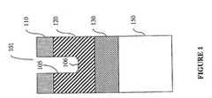
- FIG. 1illustrates the cross section of a wafer 100 having a feature 101 , such as a trench or via, in a low-k dielectric layer 120 on a substrate 150 in the middle of a low-k dielectric etching process, when a sidewall 105 and bottom surface 106 of the feature 101 have been exposed by the etching process, according to one embodiment of the present invention.
- a patterned mask layer 110partially covers the dielectric layer 120 and defines the opening of feature 101 .
- the dielectric layer 120is separated from the substrate by a barrier/liner layer 130 . Metal lines (not shown) may also lie beneath the barrier/liner layer.
- the barrier/liner layer 130acts both as a diffusion barrier between the metal lines and the dielectric layer 120 , and as an etch stop layer during the etching of the dielectric layer 120 .
- the dielectric layer 120includes a low-k dielectric material having a dielectric constant that is less than the dielectric constant of silicon dioxide (SiO 2 ), which is about 4.0.
- the thickness of the low-k dielectric layer 120is about 0.4-1.5 ⁇ m, the thickness of the mask layer 110 before etching is typically about 1930 ⁇ , and the thickness of the barrier/liner layer 130 is usually a few hundred Angstroms. As is apparent, these layers are not drawn to scale.
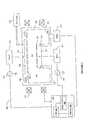
- FIG. 2depicts a schematic, cross-sectional diagram of the MERIE reactor 200 which is one example of a reactor that may be used to perform the processes of the present invention.
- the reactor 200comprises a chamber 210 enclosed by a wall 212 , a base 214 , and a ceiling 260 .
- the chamberincludes a process zone 201 comprising a volume of about 5,000 to about 50,000 cm 3 .
- the reactor 200further comprises a process gas supply 220 that supplies gaseous components into the chamber 210 through a gas manifold 262 and a gas distribution plate (GDP) 264 at the ceiling 260 of the chamber 210 , thereby forming the process gas.
- Spent process gas and volatile etch productsare pumped out from the process chamber 210 by a pump 240 .
- a throttle valve 245controls the pressure in the chamber 210 .
- the wall 212 , the base 214 , the ceiling 260 , and the GDP 264are usually made of aluminum with anodized aluminum coating on at least the surfaces facing the inside of the chamber 210 .
- the wall 212 , the base 214 , the ceiling 260 , and the GDP 264are typically grounded.
- the chamber 210further includes a pedestal 230 that supports the substrate 300 in the chamber 210 .
- the pedestal 230is electrically isolated from the base 214 by an insulator support ring 232 and is connected to a radio frequency (RF) power source 250 through an impedance match network 255 .
- the pedestal 230includes an electrostatic chuck, a vacuum chuck or other wafer holding mechanisms (not shown), and may be thermally connected to a substrate temperature control system (not shown).
- the substrate temperature control systemsuch as a resistive heating coil and/or fluid passages connected to a heating or cooling fluid system, facilitates control of the temperature of the substrate 150 during plasma processing.
- a controller 280comprising a CPU 282 , a memory 284 , and support circuits 286 for the CPU 282 is coupled to the various components of the reactor 200 to facilitate control of the etching processes of the present invention.
- the reactor configuration of FIG. 2facilitates reactive ion etching (RIE) processes, where the plasma is generated by applying RF voltage at a power level of about 100 to about 3000 Watts to the pedestal 230 while the wall 212 and ceiling 260 are grounded.
- RIEreactive ion etching
- the pedestal 230acts as a cathode electrode
- the grounded wall 212 , ceiling 260 and the GDP 264together serve as an anode electrode.
- the plasmais thus generated and maintained by capacitively coupled RF power between the cathode and the anode electrodes.
- a substantial DC biastypically exists between the plasma and the cathode electrode, resulting in energetic ion bombardment on the substrate.
- FIG. 2only shows one exemplary configuration of various types of plasma reactors that can be used to practice the present invention.
- the reactor 200may include other power sources in addition to or in place of the RF power source 250 , and power can be coupled into the chamber 210 to strike and maintain a plasma therein through differently configured coupling hardware such as known in the art, without affecting the application of the present invention.
- a reactor with two separate power supplies, a source power and a bias powermay be used to practice the present invention.
- the source powermay be an RF source power applied to an inductor coil to inductively couple energy to the plasma while the bias power is another RF source power applied to a support pedestal to bias the substrate with respect to the plasma.
- the source powermay be a very high frequency (VHF) (e.g., 50-250 MHz) power applied to a ceiling electrode while the bias power may be a RF power applied to a wafer support pedestal facing the ceiling electrode, or vice versa.
- VHFvery high frequency
- the bias powermay be a RF power applied to a wafer support pedestal facing the ceiling electrode, or vice versa.
- FIG. 3illustrates, as another example, a reactor 300 employing two separate power supplies, a RF bias power supply 350 and a VHF source power supply 370 , according to an alternative embodiment of the present invention.
- the reactor 300includes a vacuum chamber 301 enclosed by a cylindrical wall 305 and a conductive ceiling 362 .
- the wall 305 of the vacuum chamber 301is made of aluminum and is grounded.
- An inner surface 306 and outer surface 307 of the wall 305are anodized to prevent corrosion.
- a wafer support pedestal or bottom electrode 315lies at the bottom of the vacuum chamber 301 and supports the substrate 150 .
- the wafer support pedestal 315is insulated from the chamber wall 305 by an insulator ring 316 and includes mechanisms for holding the substrate 150 and for controlling the substrate temperature.
- a vacuum pump 325maintains a vacuum within the vacuum chamber 301 .
- the RF bias power supply 350 and the VHF source power supply 370are each connected to a respective one of two electrodes, a bottom electrode 315 which is also the wafer support pedestal and a top electrode 360 .
- the bottom electrodeis electrically connected to the RF bias power supply 350 through a bottom impedance match network 355 .
- the top electrode 360is in contact with the conductive ceiling 362 , which in turn is connected to the source power supply 370 through a top impedance match network 375 .
- the top electrodeis also a gas distribution plate (GDP) and has gaps or holes allowing the process gas to flow into the chamber 301 .
- GDPgas distribution plate
- a space 368is provided between the conductive plate 362 and the top electrode 360 to act as a gas distribution manifold coupled to a gas supply 340 .
- a support ring 366supports the top electrode 360 and provides insulation between the top electrode 360 and the vacuum chamber wall 305 .
- the frequencies of the bias and source power supplies 350 and 370are 13.5 MHz and 60 MHz, respectively.
- Filteringis employed to minimize the interaction between the two RF power supplies.
- such filteringis accomplished by using an inductor in the match network 375 that grounds the top electrode 360 at 13.6 MHz while appearing to be a high impedance for a 60 MHz signal.
- a capacitorcan be used in the match network 355 to ground the lower electrode 315 at 60 MHz while appearing to be a high impedance for a 13.6 MHz signal.
- the two RF power sources 350 and 370are independently controllable so that the relative amount of power coupled into the vacuum chamber 301 from the source power 370 and from the bias power source 350 can be apportioned as desired.
- the VHF source power 370controls the plasma density, due to the more efficient displacement current and sheath heating mechanisms associated with higher RF frequencies.
- the lower frequency excitation from the bias RF power source 350controls the substrate bias or the energy of the ions bombarding the wafer 150 .
- reactor 300allows separate control of the plasma density and the substrate bias.
- the operation of the reactor 300is controlled by a controller 380 comprising a CPU 382 , a memory 384 , and support circuits 386 for the CPU 382 , according to program instructions stored in memory 384 .
- the controller 380is coupled to the various components of the reactor 300 to facilitate control of the etching processes of the present invention.
- chamber 210 or 301is evacuated by pump 240 or 325 to a pressure of less than about 1 mTorr.
- the substrate 150is transferred into the chamber 210 or 301 from a load lock transfer chamber (not shown) maintained at near vacuum, and is placed on the pedestal 230 or 315 .
- Gaseous componentsare then introduced into the chamber 210 or 301 at various volumetric flow rates to form the process gas.
- the power source 250 or 370is turned on to strike a plasma of the process gas in the process zone 201 or 302 .
- the bias power 350may also be turned on and adjusted to a proper level to obtain the desired bias between the pedestal 315 and the plasma.
- the plasma densitydefined as the number of ions per unit volume, may be enhanced by placing magnets 270 around the chamber wall 212 or 305 to provide a slowly rotating magnetic field in the chamber 210 or 301 .
- the magnetsmay be electromagnets driven with respective phases of a low frequency (e.g., 0.1-0.5 Hertz) AC current source (not shown).
- the magnetsmay be permanent magnets mounted on a slowly rotating support structure (not shown) rotating at, for example, 0.1-0.5 revolutions per second.
- Plasma containing fluorocarbon or hydrofluorocarbon gashas been used to etch silicon oxides.
- the fluorocarbon or hydrofluorocarbon gascontributes fluorine and CF x species in the plasma that breaks the Si—O bond in the dielectric layer 120 .
- the etching reactionmay include, 2CF 2 +SiO 2 ⁇ SiF 4 +2CO, where the etch products SiF 4 and CO are both volatile and can be pumped out of the chamber 210 .
- the feature sidewalls 105are subject to less ion bombardment from the plasma than the feature bottom surface 106 , these passivating deposits accumulate more on the feature sidewalls 105 , resulting in enhanced anisotropic etching.
- the CF x speciesare considered crucial in achieving anisotropic etching profile.
- many etching chemistries for etching silicon dioxide filmsuse fluorocarbon gases with relatively high carbon to fluorine ratios, such as C 2 F 6 , C 4 F 6 , etc., in order to provide enough passivating deposits for sidewall protection.
- fluorine-rich fluorocarbon or hydrofluorocarbon gasesexamples include CF 4 , C 2 F 8 , CHF 3 , etc., of which CF 4 is more often preferred.
- the more complicated chemical compositions in the low-k dielectric layer 320often require more complicated chemistry in the process gas.
- a nitrogen-containing gas in the process gashas been found to help in breaking the Si—CH 3 bond without adversely impacting the etching selectivity to photoresist.
- adding a certain amount of N 2 to a CF 4 based process gas or a CF 4 /CHF 3 mixture based process gasresults in significant increase in the low-k dielectric etch rate.
- the process gas in one embodiment of the present inventionoften includes a nitrogen containing gas.
- Suitable nitrogen containing gasesinclude N 2 , NH 3 , NF 3 , of which N 2 is more often used.
- FIGS. 4A and 4Balso show that the low-k dielectric etch rate starts to drop when the volumetric flow rate ratio (or flow ratio) of N 2 :CF 4 or N 2 :CF 4 /CHF 3 increases beyond 0.4 or 0.3, respectively, therefore there may exist an optimum range of the N 2 :CF 4 or N 2 :CF 4 /CHF 3 flow ratio depending on specific application.
- the process gasoften includes one or more additive gases, such as a hydrogen-containing gas, an inert gas, and/or a carbon-oxygen gas.
- the hydrogen-containing gascan be added to provide hydrogen or hydrogen-containing radicals in the etching plasma that, when combined with nitrogen or nitrogen-containing radicals, break the S 1 —CH 3 bond faster, resulting in faster etch rate and higher etching selectivity to photoresist.
- Suitable hydrogen-containing gasesinclude hydrogen-rich hydrofluorocarbon gases such as CH 2 F 2 , CH 3 F, etc.
- the etching reactionmay include Si—CH 3 +H* ⁇ Si—CH, and Si—CH+F*+N* ⁇ SiF x +C ⁇ H ⁇ N ⁇ where ⁇ , ⁇ , and ⁇ are integers, and the etch products C ⁇ H ⁇ N ⁇ are typically volatile.
- Other possible by-products resulting from the interactions between the plasma and the low-k dielectric layermay include CO, CN, NH x , NF x , HF, C 3 H 2 , etc.
- a hydrogen-rich fluorocarbon gasas the hydrogen-containing gas has also been found to help widening the process window and therefore improving etch rate microloading and etch rate uniformity across the substrate.
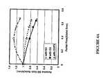
- FIG. 5Awhen a CH 2 F 2 gas is added to a CF 4 -based plasma, etch rate microloading rapidly drops, indicating a much wider process window.
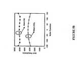
- FIG. 5Billustrates the etch rate uniformity of a blanket low-k dielectric layer across a 300 mm substrate when a CF 4 /N 2 /CH 2 F 2 process gas is used.
- the etch rateincreases sharply and there is significant improvement in the etching selectivity with respect to a photoresist mask.
- the etch ratestarts to drop when the CH 2 F 2 :CF 4 flow rate ratio further increases beyond 0.5. Therefore, there may exist an optimum range for the CH 2 F 2 :CF 4 flow rate ratio depending on specific application.
- an inert gas in the process gashas been found to help controlling the etched feature profile. This is possibly due to the inert ions in the etching plasma that impinge mostly on the bottom surface 106 of the etched feature 101 , activating chemical reactions thereon while leaving the sidewalls 105 of the feature less affected.
- the inert ionsalso help to reduce etch product deposits by sputtering them off the feature surfaces.
- Suitable inert gasesinclude argon, helium, neon, xenon, and krypton, of which argon is more often preferred.
- a carbon-oxygen gashas been found to improve the etching selectivity to the barrier/liner layer, which often includes a silicon carbide material.
- a suitable carbon-oxygen gasis CO.
- the volumetric flow rate of each gas in the process gasdepends on many factors, including the configuration of the reactor used to carry out the etching process, the size of the substrate, and the specific gases used in the process gas.
- the volumetric flow ratios of the different gases in the process gascan also be tailored for different combinations of materials and to achieve specific etching selectivities, etch rates, or feature geometry without deviating from the scope of the present invention.
- the flow ratio of N 2 :CF 4is about 1:4 to 2:1, and the flow ratio of CH 2 F 2 :CF 4 is about 1:3 to 1:1, and more often about 1:3 to 1:2. Relatively high volumetric flow of the inert gas has been found to achieve optimum profile.
- the process gasincludes argon as the inert gas, the flow ratio of argon to the fluorocarbon gas is from about 20:1 to 50:1.
- substrate 150is a silicon wafer of 200 mm (8 inch) or 100 mm (12 inch) diameter. As shown in FIG. 1 , the wafer 150 is coated successively with the barrier/liner layer 130 having a thickness of a few hundred angstroms, the low-k dielectric layer 120 having a thickness of about 0.4-1.5 micron, and a mask layer 110 of about 1930 ⁇ that is patterned to define features such as feature 101 to be etched.
- the mask layeris photoresist, such as “RISTON,” manufactured by duPont de Nemours Chemical Company.
- the low-k dielectric layercomprises carbon-doped dielectrics such as CH 3 doped organo-silicate glass (OSG), organic polymers (e.g. benzocyclobutene, parylene, polytetrafluoroethylene, polyether, polyimide) or the like that are doped with a carbon-based dopant (e.g. CH 3 ).
- the OSGis sometimes referred to as doped silicon dioxide, examples of which are Black DiamondTM I and Black DiamondTM II, which is an improved version of the Black DiamondTM I with higher carbon content than Black DiamondTM I.
- Both Black DiamondTM I and Black DiamondTM IIare available from Applied Materials of Santa Clara, Calif.
- Other examples of the OSGare CoralTM from Novellus of San Jose, Calif., and Sumika FilmTM from Sumitomo Chemical America, Inc., Santa Clara, Calif.
- the OSG layeris grown using chemical vapor deposition by oxidizing methyl silane, as disclosed by Yau et al. in U.S. Pat. Nos. 6,054,379 and 6,072,227.
- the number of methyl radicals in this and related materialsmay vary from one to four for a monosilane.
- the barrier/liner layeris a BLOkTM (barrier low-k) film, which is a silicon carbide film formed using the chemical vapor deposition (CVD) or plasma enhanced CVD process described in commonly owned U.S. Pat. No. 6,287,990 B1, issued Sep. 11, 2001, and U.S. Pat. No. 6,303,523 B2, issued Oct. 16, 2001, which are incorporated herein by reference.
- the BLOkTM filmsinclude BLOkTM I and BLOkTM II, which is an improved version of BLOkTM I, both of which are available from Applied Materials of Santa Clara, Calif.
- Various layers of other materialsmay lie under the barrier/liner layer, which should not affect the practice of the present invention.
- a thin (600 ⁇ ) antireflective coating (ARC) or bottom antireflective coating (BARC) layer (not shown) and a hard mask layermay lie between the mask layer 310 and the OSG layer 320 .
- the ARC (or BARC layer)is typically used for line/width control during photolithography when the minimum feature sizes reach below quarter micron.
- a conventional ARC (or BARC) open processcan be performed to clear away the ARC (or BARC layer) at the feature openings before etching the low-k dielectric layer.
- the hard mask layeris typically made of a conventional dielectric material such as silicon dioxide and is used as a stop layer during a subsequent CMP process for creating damascene of dual-damascene structures.
- a conventional hard mask etching processcan be used to clear away portions of the hard mask layer at the feature openings before etching the low-k dielectric layer.
- FIG. 6is a flow chart illustrating a process sequence 600 for etching the dielectric layer 120 in the reactor 200 shown in FIG. 2 or in the reactor 300 shown in FIG. 3 , according to two exemplary embodiments of the present invention.
- the sequence 600includes an optional step 602 , in which the magnets 270 are turned on to create a magnetic field in the process chamber 210 or 301 above the wafer substrate 150 .
- the sequence 600further includes step 604 , in which wafer temperature (or cathode temperature) is set and further maintained at a predetermined value by controlling, e.g., a flow of the backside gas such as He.
- the wafer temperatureis maintained sufficiently high to volatilize most of the etch products, and sufficiently low so that a layer of passivating deposits and etch product deposits is retained on the sidewalls 105 of freshly etched feature 101 .
- the chamber wall 212 or 305is also kept at a controlled temperature level, such as about 15° C., using a conventional cooling or heating mechanism as necessary for maintaining the chamber wall temperature.
- the sequence 600further includes step 606 , in which the process gas is supplied to the process chamber 210 or 301 through the gas distribution plate 264 or 360 .
- the sequence 600further includes step 608 , in which the pressure of the process gas in the process chamber 210 or 301 is adjusted by regulating at least one process parameter such as the flow rate of one or more gaseous components, or a position of the throttle valve 225 or 325 , respectively.
- the sequence 600further includes step 610 , in which the VHF source power 370 ignites the process gas in processing chamber 301 to form the plasma by applying power from the VHF source 370 to the top electrode 360 . Thereafter or about simultaneously with igniting the plasma, at step 612 in the process sequence 600 , the RF bias power 350 is turned on to electrically bias the wafer support pedestal.
- step 610 and step 612are both accomplished by turning on the RF power 250 , which ignites the process gas in processing chamber 210 as well as biases the wafer support pedestal.
- the process sequence 600further includes step 614 , in which the dielectric layer 120 is etched using plasma 152 to form a plurality of features including feature 101 in the dielectric layer 120 .
- step 614etches Black DiamondTM with a selectivity to BLokTM layer of about 10:1 or greater and a selectivity to a photoresist mask of about 5:1 or greater.
- Step 614continues for a predetermined time period or is terminated using a conventional optical endpoint measurement technique that determines, by monitoring emissions from the plasma, whether the bottom surfaces (such as surface 106 in feature 101 ) in the plurality of features has reached the top of the etch stop layer 130 .
- the plasmais turned off by turning off the VHF source power 370 and/or the bias source 250 or 350 .
- the magnets 270may be turned off also and the process gas supply is stopped. Then the wafer is dechucked and removed from the processing chamber 210 or 301 .
- sequence 600is performed by the controller 280 shown in FIG. 2 or the controller 380 shown in FIG. 3 , according to program instructions stored in memory 284 or 384 , respectively.
- some or all of the steps in the sequence 600may be performed in hardware such as an application-specific integrated circuit (ASIC) or other type of hardware implementation, or a combination of software or hardware.
- ASICapplication-specific integrated circuit
- Table I and IIsummarizes the ranges, i.e., minimum and maximum values, and exemplary values of several process parameters used to etch the low-k dielectric layer 320 on a 300 mm wafer using the etch reactor 300 shown in FIG. 3 .
- Table III and IVlist some of the process parameters such as RF power, pressure, process gas composition and flow rates, etc. used in several exemplary processes for etching the dielectric layer 320 on a 300 mm wafer in reactor 200 .
- Example 140 20 2000 20 100 2000 15° C.
- Example 260 60 2000 30 100 2000 15° C.
- Example 360 60 2000 30 100 2000 30° C.
- process parameterssuch as the RF power, pressure, gas flow rates, etc.
- process parametersare dependent upon the size of the wafer, the volume of the chamber, and on other hardware configurations of the reactor used to practice the present invention, the invention is not limited to process parameters or the ranges recited herein.
Landscapes
- Engineering & Computer Science (AREA)
- Physics & Mathematics (AREA)
- Chemical & Material Sciences (AREA)
- Condensed Matter Physics & Semiconductors (AREA)
- General Physics & Mathematics (AREA)
- Manufacturing & Machinery (AREA)
- Computer Hardware Design (AREA)
- Microelectronics & Electronic Packaging (AREA)
- Power Engineering (AREA)
- Chemical Kinetics & Catalysis (AREA)
- General Chemical & Material Sciences (AREA)
- Inorganic Chemistry (AREA)
- Plasma & Fusion (AREA)
- Drying Of Semiconductors (AREA)
Abstract
Description
- The present application relates to semiconductor processing technologies, and particularly to etching patterns in a layer of dielectric material having low dielectric constant.
- The maximum operating speed of current semiconductor devices is limited by the time delay factor T=RC of metal lines, where R is the resistance of the metal lines and C is the capacitance of the dielectric insulating material surrounding the metal lines. As the minimum feature size of integrated circuits continues to shrink, the metal lines become thinner and more densely packed, resulting in greater resistance in the metal lines and larger inter-metal capacitance, and therefore a longer time delay. By changing to different materials, i.e., higher conductivity material for the metal lines and lower permittivity (low-k) dielectric for the insulating material, device geometry can continue to shrink without adversely impacting the maximum operating speed. This has prompted the switch from aluminum and silicon dioxide to copper and low-k dielectrics such as organosilicate glass in the backend process flow for manufacturing many current and future semiconductor devices.
- The switch from aluminum/oxide to copper/low-k involves a variety of fundamental changes in the backend manufacturing process flow. Since it is difficult to etch copper, new approaches such as “damascene” or “dual damascene” processing are required. Copper damascene/dual-damascene is a process where vias and trenches are etched into the insulating material. Copper is then filled into the vias and trenches and sanded back so the conducting materials are only left in the vias and trenches. Among the many challenges presented by this process, etching trenches or vias in low-k dielectrics can be tricky due to the more complicated chemical composition of the dielectric material and the many different kinds of low-k dielectric materials available. The etch chemistry for etching a low-k dielectric material may have to be tailored to match up with the amount of carbon, hydrogen, silicon, fluorine and oxygen in the material.
- The ratio of the rate of etching a low-k dielectric layer to the rate of etching one of the adjacent layers of other materials is called etching selectivity. A photoresist layer is typically used to mask the low-k dielectric layer during the etching process. As the feature sizes continue to shrink, the photoresist mask becomes thinner in order to meet lithography-related challenges posed by smaller feature sizes. The thinner resist requires tighter control on the dielectric etch selectivity. However, like photoresist, many low-k dielectric materials also contain some carbon and hydrogen, making it harder to meet the selectivity requirement. Therefore, compared with traditional dielectric etching processes, selectively etching low-k dielectric materials requires more precise tuning of the process chemistry and process parameters.
- Another problem associated with etching low-k dielectrics is the dependence of the low-k dielectric etch rate upon pattern density and topographic dimensions of etched features (e.g. vias and trenches), which is known as etch rate microloading, or microloading. The etch rate microloading is a measure of the difference in etch rate in features having different sizes, and is calculated as a percent value of the difference between etch rate in a larger feature and etch rate in a smaller feature divided by the etch rate in the larger feature. It has been noted that microloading increases as the size of an opening of the small feature decreases and as the aspect ratio of the small feature increases.
- The present invention provides a process for etching a low-k dielectric layer with improved selectivity to adjacent layers and reduced microloading as compared to conventional low-k dielectric etching processes. In one embodiment of the present invention, the low-k dielectric layer is formed on a substrate with an underlying barrier/liner layer and an overlying photoresist mask. The substrate is placed in a plasma etch chamber and a plasma of a gas mixture is turned on and maintained in the plasma etch chamber to etch the low-k dielectric layer. The gas mixture comprises a fluorine-rich fluorocarbon or hydrofluorocarbon gas, such as CF4, C2F8, CHF3, C2F6, etc., a nitrogen-containing gas, such as N2, NH3, NF3, etc., and one or more additive gases, such as an inert gas, a hydrogen-containing gas, and/or a carbon-oxygen gas.
- Additional objects and features of the invention will be more readily apparent from the following detailed description and appended claims when taken in conjunction with the drawings, in which:
FIG. 1 is a schematic view in vertical cross-section of a trench or via in a dielectric layer in the middle of an etching process;FIG. 2 is a schematic view in vertical cross-section of a plasma reactor used to practice a low-k dielectric etching process according to one embodiment of the present invention;FIG. 3 is a schematic view in vertical cross-section of a plasma reactor used to practice a low-k dielectric etching process according to an alternative embodiment of the present invention;FIG. 4A is a chart showing changes in low-k dielectric etch rate in response to different additives to a fluorocarbon based plasma;FIG. 4B is a chart showing changes in low-k dielectric etch rate in response to different additives to a fluorocarbon/hydrofluorocarbon mixture based plasma;FIG. 5A is a chart showing the trend of change in low-k dielectric etch rate, etching selectivity to photoresist, and microloading in response to change in CH2F2/CF4flow ratio according to one embodiment of the present invention;FIG. 5B is a chart showing the low-k dielectric etch rate uniformity across a 300 mm substrate, according to one embodiment of the present invention;FIG. 6 is a flow chart illustrating a process sequence for etching a low-k dielectric material according to one embodiment of the present invention.- The etching process of the present invention is useful for etching a low-k dielectric layer with good etch rate and high etching selectivities with respect to an overlying mask layer and an underlying barrier/liner layer. As will be described in more detail below, the etching process is performed by exposing portions of the low-k dielectric layer not covered by the mask layer to an energized gas, such as a plasma, comprising energetic and reactive species. The plasma is usually generated in a plasma reactor, such as, for example, a magnetically enhanced reactive ion etching (MERIE) reactor, or a dual frequency capacitive plasma source etch reactor used as a part of the CENTURA® semiconductor wafer processing system, available from Applied Materials Inc., Santa Clara, Calif.
- The low-k dielectric layer is typically formed on a substrate and patterned with a mask that defines features to be etched.
FIG. 1 illustrates the cross section of awafer 100 having afeature 101, such as a trench or via, in a low-kdielectric layer 120 on asubstrate 150 in the middle of a low-k dielectric etching process, when asidewall 105 andbottom surface 106 of thefeature 101 have been exposed by the etching process, according to one embodiment of the present invention. Apatterned mask layer 110 partially covers thedielectric layer 120 and defines the opening offeature 101. In some applications, thedielectric layer 120 is separated from the substrate by a barrier/liner layer 130. Metal lines (not shown) may also lie beneath the barrier/liner layer. In some applications, the barrier/liner layer 130 acts both as a diffusion barrier between the metal lines and thedielectric layer 120, and as an etch stop layer during the etching of thedielectric layer 120. - In one embodiment of the present invention, the
dielectric layer 120 includes a low-k dielectric material having a dielectric constant that is less than the dielectric constant of silicon dioxide (SiO2), which is about 4.0. The thickness of the low-kdielectric layer 120 is about 0.4-1.5 μm, the thickness of themask layer 110 before etching is typically about 1930 Å, and the thickness of the barrier/liner layer 130 is usually a few hundred Angstroms. As is apparent, these layers are not drawn to scale. FIG. 2 depicts a schematic, cross-sectional diagram of the MERIEreactor 200 which is one example of a reactor that may be used to perform the processes of the present invention. Thereactor 200 comprises achamber 210 enclosed by awall 212, abase 214, and aceiling 260. The chamber includes aprocess zone 201 comprising a volume of about 5,000 to about 50,000 cm3. Thereactor 200 further comprises aprocess gas supply 220 that supplies gaseous components into thechamber 210 through agas manifold 262 and a gas distribution plate (GDP)264 at theceiling 260 of thechamber 210, thereby forming the process gas. Spent process gas and volatile etch products are pumped out from theprocess chamber 210 by apump 240. Athrottle valve 245 controls the pressure in thechamber 210. Thewall 212, thebase 214, theceiling 260, and theGDP 264 are usually made of aluminum with anodized aluminum coating on at least the surfaces facing the inside of thechamber 210. Thewall 212, thebase 214, theceiling 260, and theGDP 264 are typically grounded.- The
chamber 210 further includes apedestal 230 that supports thesubstrate 300 in thechamber 210. Thepedestal 230 is electrically isolated from thebase 214 by aninsulator support ring 232 and is connected to a radio frequency (RF)power source 250 through animpedance match network 255. Thepedestal 230 includes an electrostatic chuck, a vacuum chuck or other wafer holding mechanisms (not shown), and may be thermally connected to a substrate temperature control system (not shown). The substrate temperature control system, such as a resistive heating coil and/or fluid passages connected to a heating or cooling fluid system, facilitates control of the temperature of thesubstrate 150 during plasma processing. - A
controller 280 comprising aCPU 282, amemory 284, and supportcircuits 286 for theCPU 282 is coupled to the various components of thereactor 200 to facilitate control of the etching processes of the present invention. - The reactor configuration of
FIG. 2 facilitates reactive ion etching (RIE) processes, where the plasma is generated by applying RF voltage at a power level of about 100 to about 3000 Watts to thepedestal 230 while thewall 212 andceiling 260 are grounded. With theRF source 250 turned on, thepedestal 230 acts as a cathode electrode, while the groundedwall 212,ceiling 260 and theGDP 264 together serve as an anode electrode. The plasma is thus generated and maintained by capacitively coupled RF power between the cathode and the anode electrodes. A substantial DC bias typically exists between the plasma and the cathode electrode, resulting in energetic ion bombardment on the substrate. FIG. 2 only shows one exemplary configuration of various types of plasma reactors that can be used to practice the present invention. For example, thereactor 200 may include other power sources in addition to or in place of theRF power source 250, and power can be coupled into thechamber 210 to strike and maintain a plasma therein through differently configured coupling hardware such as known in the art, without affecting the application of the present invention. For example, a reactor with two separate power supplies, a source power and a bias power, may be used to practice the present invention. The source power may be an RF source power applied to an inductor coil to inductively couple energy to the plasma while the bias power is another RF source power applied to a support pedestal to bias the substrate with respect to the plasma. Alternatively, the source power may be a very high frequency (VHF) (e.g., 50-250 MHz) power applied to a ceiling electrode while the bias power may be a RF power applied to a wafer support pedestal facing the ceiling electrode, or vice versa.FIG. 3 illustrates, as another example, areactor 300 employing two separate power supplies, a RFbias power supply 350 and a VHFsource power supply 370, according to an alternative embodiment of the present invention. Thereactor 300 includes avacuum chamber 301 enclosed by acylindrical wall 305 and aconductive ceiling 362. In one embodiment of the present invention, thewall 305 of thevacuum chamber 301 is made of aluminum and is grounded. Aninner surface 306 andouter surface 307 of thewall 305 are anodized to prevent corrosion. A wafer support pedestal orbottom electrode 315 lies at the bottom of thevacuum chamber 301 and supports thesubstrate 150. Thewafer support pedestal 315 is insulated from thechamber wall 305 by aninsulator ring 316 and includes mechanisms for holding thesubstrate 150 and for controlling the substrate temperature. Avacuum pump 325 maintains a vacuum within thevacuum chamber 301.- The RF bias
power supply 350 and the VHFsource power supply 370 are each connected to a respective one of two electrodes, abottom electrode 315 which is also the wafer support pedestal and atop electrode 360. The bottom electrode is electrically connected to the RF biaspower supply 350 through a bottomimpedance match network 355. Thetop electrode 360 is in contact with theconductive ceiling 362, which in turn is connected to thesource power supply 370 through a topimpedance match network 375. In one embodiment of the present invention, the top electrode is also a gas distribution plate (GDP) and has gaps or holes allowing the process gas to flow into thechamber 301. For that purpose, aspace 368 is provided between theconductive plate 362 and thetop electrode 360 to act as a gas distribution manifold coupled to agas supply 340. Asupport ring 366 supports thetop electrode 360 and provides insulation between thetop electrode 360 and thevacuum chamber wall 305. - In one embodiment of the present invention, the frequencies of the bias and source power supplies350 and370 are 13.5 MHz and 60 MHz, respectively. Filtering is employed to minimize the interaction between the two RF power supplies. In one embodiment of the present invention, such filtering is accomplished by using an inductor in the
match network 375 that grounds thetop electrode 360 at 13.6 MHz while appearing to be a high impedance for a 60 MHz signal. Similarly, a capacitor can be used in thematch network 355 to ground thelower electrode 315 at 60 MHz while appearing to be a high impedance for a 13.6 MHz signal. Therefore, the twoRF power sources vacuum chamber 301 from thesource power 370 and from thebias power source 350 can be apportioned as desired. To a fair approximation, theVHF source power 370 controls the plasma density, due to the more efficient displacement current and sheath heating mechanisms associated with higher RF frequencies. The lower frequency excitation from the biasRF power source 350 controls the substrate bias or the energy of the ions bombarding thewafer 150. Thus,reactor 300 allows separate control of the plasma density and the substrate bias. - In one embodiment of the present invention, the operation of the
reactor 300 is controlled by acontroller 380 comprising aCPU 382, amemory 384, and supportcircuits 386 for theCPU 382, according to program instructions stored inmemory 384. Thecontroller 380 is coupled to the various components of thereactor 300 to facilitate control of the etching processes of the present invention. - To perform the etching processes of the present invention using either
reactor 200 orreactor 300,chamber pump substrate 150 is transferred into thechamber pedestal chamber chamber 210 is stabilized at a desired level, thepower source process zone reactor 300 is used, thebias power 350 may also be turned on and adjusted to a proper level to obtain the desired bias between thepedestal 315 and the plasma. The plasma density, defined as the number of ions per unit volume, may be enhanced by placingmagnets 270 around thechamber wall chamber - Plasma containing fluorocarbon or hydrofluorocarbon gas has been used to etch silicon oxides. The fluorocarbon or hydrofluorocarbon gas contributes fluorine and CFxspecies in the plasma that breaks the Si—O bond in the
dielectric layer 120. The etching reaction may include,
2CF2+SiO2→SiF4+2CO,
where the etch products SiF4and CO are both volatile and can be pumped out of thechamber 210. At the same time, some CFxspecies (x=1, 2, 3) may form polymeric passivating deposits on the feature surfaces by recombining with each other or with other species before reacting with the dielectric layer. Because thefeature sidewalls 105 are subject to less ion bombardment from the plasma than the featurebottom surface 106, these passivating deposits accumulate more on thefeature sidewalls 105, resulting in enhanced anisotropic etching. In fact, during the etching of conventional dielectrics such as silicon dioxide films, the CFxspecies are considered crucial in achieving anisotropic etching profile. Thus, many etching chemistries for etching silicon dioxide films use fluorocarbon gases with relatively high carbon to fluorine ratios, such as C2F6, C4F6, etc., in order to provide enough passivating deposits for sidewall protection. - The use of a fluorocarbon gas with a relatively high carbon to fluorine ratio, however, often results in slower etch rate and larger microloading. The inventors of the present invention have found that, when etching carbon-doped low-k dielectrics, the presence of carbon in the low-k dielectrics allows the use of fluorine-rich fluorocarbon or hydrofluorocarbon gases, i.e., fluorocarbon or hydrofluorocarbon gases with relatively low carbon to fluorine ratios. Examples of the fluorine-rich fluorocarbon or hydrofluorocarbon gases include CF4, C2F8, CHF3, etc., of which CF4is more often preferred. Because of the release of carbon during the etching processes from the low-k dielectrics, especially low-k dielectrics with relatively high amount of carbon content (e.g. more than 8% carbon), enough sidewall protection can be achieved with the use of the fluorine-rich fluorocarbon or hydro-fluorocarbon gases. As a result, the use of a fluorine-rich fluorocarbon or hydrofluorocarbon gas in a low-k dielectric etching process often results in a higher low-k dielectric etch rate, better selectivity to photoresist mask, and a smaller amount of microloading.
- The more complicated chemical compositions in the low-k dielectric layer320 often require more complicated chemistry in the process gas. For low-k dielectrics such as carbon-doped silicon dioxide films containing alkyl groups such as CH3, a nitrogen-containing gas in the process gas has been found to help in breaking the Si—CH3bond without adversely impacting the etching selectivity to photoresist. As shown in
FIGS. 4A and 4B , adding a certain amount of N2to a CF4based process gas or a CF4/CHF3mixture based process gas results in significant increase in the low-k dielectric etch rate. Thus the process gas in one embodiment of the present invention often includes a nitrogen containing gas. Suitable nitrogen containing gases include N2, NH3, NF3, of which N2is more often used.FIGS. 4A and 4B also show that the low-k dielectric etch rate starts to drop when the volumetric flow rate ratio (or flow ratio) of N2:CF4or N2:CF4/CHF3increases beyond 0.4 or 0.3, respectively, therefore there may exist an optimum range of the N2:CF4or N2:CF4/CHF3flow ratio depending on specific application. - Besides the fluorine-rich fluorocarbon or hydrofluorocarbon gas and the nitrogen-containing gas, the process gas often includes one or more additive gases, such as a hydrogen-containing gas, an inert gas, and/or a carbon-oxygen gas. The hydrogen-containing gas can be added to provide hydrogen or hydrogen-containing radicals in the etching plasma that, when combined with nitrogen or nitrogen-containing radicals, break the S1—CH3bond faster, resulting in faster etch rate and higher etching selectivity to photoresist. Suitable hydrogen-containing gases include hydrogen-rich hydrofluorocarbon gases such as CH2F2, CH3F, etc. With the nitrogen-containing gas and the hydrogen-containing gas in the process gas, the etching reaction may include
Si—CH3+H*→Si—CH, and Si—CH+F*+N*→SiFx+CαHβNγ
where α, β, and γ are integers, and the etch products CαHβNγare typically volatile. Other possible by-products resulting from the interactions between the plasma and the low-k dielectric layer may include CO, CN, NHx, NFx, HF, C3H2, etc. - The addition of a hydrogen-rich fluorocarbon gas as the hydrogen-containing gas has also been found to help widening the process window and therefore improving etch rate microloading and etch rate uniformity across the substrate. As shown in
FIG. 5A , when a CH2F2gas is added to a CF4-based plasma, etch rate microloading rapidly drops, indicating a much wider process window. The improved process window is also manifested by the good etch uniformity resulting from the addition of the hydrogen-rich fluorocarbon gas, as shown inFIG. 5B , which illustrates the etch rate uniformity of a blanket low-k dielectric layer across a 300 mm substrate when a CF4/N2/CH2F2process gas is used. Also, as shown inFIG. 5A , with the addition of the CH2F2gas, the etch rate increases sharply and there is significant improvement in the etching selectivity with respect to a photoresist mask. The etch rate starts to drop when the CH2F2:CF4flow rate ratio further increases beyond 0.5. Therefore, there may exist an optimum range for the CH2F2:CF4flow rate ratio depending on specific application. - The addition of an inert gas in the process gas has been found to help controlling the etched feature profile. This is possibly due to the inert ions in the etching plasma that impinge mostly on the
bottom surface 106 of theetched feature 101, activating chemical reactions thereon while leaving thesidewalls 105 of the feature less affected. The inert ions also help to reduce etch product deposits by sputtering them off the feature surfaces. Suitable inert gases include argon, helium, neon, xenon, and krypton, of which argon is more often preferred. - The addition of a carbon-oxygen gas has been found to improve the etching selectivity to the barrier/liner layer, which often includes a silicon carbide material. A suitable carbon-oxygen gas is CO.
- The volumetric flow rate of each gas in the process gas depends on many factors, including the configuration of the reactor used to carry out the etching process, the size of the substrate, and the specific gases used in the process gas. The volumetric flow ratios of the different gases in the process gas can also be tailored for different combinations of materials and to achieve specific etching selectivities, etch rates, or feature geometry without deviating from the scope of the present invention. In one embodiment of the present invention, when the process gas includes CF4as the fluorocarbon gas, N2as the nitrogen-containing gas, and CH2F2as the hydrogen-rich hydrofluorocarbon gas, the flow ratio of N2:CF4is about 1:4 to 2:1, and the flow ratio of CH2F2:CF4is about 1:3 to 1:1, and more often about 1:3 to 1:2. Relatively high volumetric flow of the inert gas has been found to achieve optimum profile. In one embodiment of the present invention, when the process gas includes argon as the inert gas, the flow ratio of argon to the fluorocarbon gas is from about 20:1 to 50:1.
- The following examples illustrate use of the present invention for etching the low-
k dielectric layer 120 onsubstrate 150. An example ofsubstrate 150 is a silicon wafer of 200 mm (8 inch) or 100 mm (12 inch) diameter. As shown inFIG. 1 , thewafer 150 is coated successively with the barrier/liner layer 130 having a thickness of a few hundred angstroms, the low-k dielectric layer 120 having a thickness of about 0.4-1.5 micron, and amask layer 110 of about 1930 Å that is patterned to define features such asfeature 101 to be etched. - In the following examples, the mask layer is photoresist, such as “RISTON,” manufactured by duPont de Nemours Chemical Company. The low-k dielectric layer comprises carbon-doped dielectrics such as CH3doped organo-silicate glass (OSG), organic polymers (e.g. benzocyclobutene, parylene, polytetrafluoroethylene, polyether, polyimide) or the like that are doped with a carbon-based dopant (e.g. CH3). The OSG is sometimes referred to as doped silicon dioxide, examples of which are Black Diamond™ I and Black Diamond™ II, which is an improved version of the Black Diamond™ I with higher carbon content than Black Diamond™ I. Both Black Diamond™ I and Black Diamond™ II are available from Applied Materials of Santa Clara, Calif. Other examples of the OSG are Coral™ from Novellus of San Jose, Calif., and Sumika Film™ from Sumitomo Chemical America, Inc., Santa Clara, Calif. In the case of Black Diamond™ I, the OSG layer is grown using chemical vapor deposition by oxidizing methyl silane, as disclosed by Yau et al. in U.S. Pat. Nos. 6,054,379 and 6,072,227. The number of methyl radicals in this and related materials may vary from one to four for a monosilane.
- The barrier/liner layer is a BLOk™ (barrier low-k) film, which is a silicon carbide film formed using the chemical vapor deposition (CVD) or plasma enhanced CVD process described in commonly owned U.S. Pat. No. 6,287,990 B1, issued Sep. 11, 2001, and U.S. Pat. No. 6,303,523 B2, issued Oct. 16, 2001, which are incorporated herein by reference. The BLOk™ films include BLOk™ I and BLOk™ II, which is an improved version of BLOk™ I, both of which are available from Applied Materials of Santa Clara, Calif. Various layers of other materials may lie under the barrier/liner layer, which should not affect the practice of the present invention.
- A thin (600 Å) antireflective coating (ARC) or bottom antireflective coating (BARC) layer (not shown) and a hard mask layer may lie between the mask layer310 and the OSG layer320. The ARC (or BARC layer) is typically used for line/width control during photolithography when the minimum feature sizes reach below quarter micron. A conventional ARC (or BARC) open process can be performed to clear away the ARC (or BARC layer) at the feature openings before etching the low-k dielectric layer. The hard mask layer is typically made of a conventional dielectric material such as silicon dioxide and is used as a stop layer during a subsequent CMP process for creating damascene of dual-damascene structures. A conventional hard mask etching process can be used to clear away portions of the hard mask layer at the feature openings before etching the low-k dielectric layer.
FIG. 6 is a flow chart illustrating aprocess sequence 600 for etching thedielectric layer 120 in thereactor 200 shown inFIG. 2 or in thereactor 300 shown inFIG. 3 , according to two exemplary embodiments of the present invention. Thesequence 600 includes anoptional step 602, in which themagnets 270 are turned on to create a magnetic field in theprocess chamber wafer substrate 150. Thesequence 600 further includesstep 604, in which wafer temperature (or cathode temperature) is set and further maintained at a predetermined value by controlling, e.g., a flow of the backside gas such as He.- The wafer temperature is maintained sufficiently high to volatilize most of the etch products, and sufficiently low so that a layer of passivating deposits and etch product deposits is retained on the
sidewalls 105 of freshly etchedfeature 101. Thechamber wall - The
sequence 600 further includesstep 606, in which the process gas is supplied to theprocess chamber gas distribution plate sequence 600 further includesstep 608, in which the pressure of the process gas in theprocess chamber throttle valve 225 or325, respectively. - When
reactor 300 is used, thesequence 600 further includesstep 610, in which theVHF source power 370 ignites the process gas inprocessing chamber 301 to form the plasma by applying power from theVHF source 370 to thetop electrode 360. Thereafter or about simultaneously with igniting the plasma, atstep 612 in theprocess sequence 600, theRF bias power 350 is turned on to electrically bias the wafer support pedestal. Whenreactor 200 is used,step 610 and step612 are both accomplished by turning on theRF power 250, which ignites the process gas inprocessing chamber 210 as well as biases the wafer support pedestal. - The
process sequence 600 further includesstep 614, in which thedielectric layer 120 is etched using plasma152 to form a plurality offeatures including feature 101 in thedielectric layer 120. In one embodiment of the present invention, step614 etches Black Diamond™ with a selectivity to BLok™ layer of about 10:1 or greater and a selectivity to a photoresist mask of about 5:1 or greater. Step614 continues for a predetermined time period or is terminated using a conventional optical endpoint measurement technique that determines, by monitoring emissions from the plasma, whether the bottom surfaces (such assurface 106 in feature101) in the plurality of features has reached the top of theetch stop layer 130. Thereafter, atstep 616 in theprocess sequence 600, the plasma is turned off by turning off theVHF source power 370 and/or thebias source magnets 270 may be turned off also and the process gas supply is stopped. Then the wafer is dechucked and removed from theprocessing chamber - The foregoing steps of the
sequence 600 need not be performed sequentially, e.g., some or all of the steps may be performed simultaneously or in different order. In one embodiment of the present invention,sequence 600 is performed by thecontroller 280 shown inFIG. 2 or thecontroller 380 shown inFIG. 3 , according to program instructions stored inmemory sequence 600 may be performed in hardware such as an application-specific integrated circuit (ASIC) or other type of hardware implementation, or a combination of software or hardware. - Table I and II summarizes the ranges, i.e., minimum and maximum values, and exemplary values of several process parameters used to etch the low-k dielectric layer320 on a 300 mm wafer using the
etch reactor 300 shown inFIG. 3 .TABLE I Process Parameters Minimum Maximum Example Process Gas CF 4 2 200 20 Flow Rate (sccm) N2 4 400 40 CH2F2 4 400 40 Ar 500 — 2000 Source Power (W) 100 300 200 Bias Power (W) 1500 2500 2000 Chamber Pressure (mTorr) 60 150 100 Wafer Pedestal Temperature (° C.) 0 30 20 TABLE II Process Parameters Minimum Maximum Example Process Gas CF 4 50 80 65 Flow Rate (sccm) N 250 200 170 Ar 100 1500 500 CO 0 300 2000 Source Power (W) 0 1000 300 Bias Power (W) 1000 3000 2800 Chamber Pressure (mTorr) 10 150 30 Cathode Temperature (° C.) −20 40 −10 - Table III and IV list some of the process parameters such as RF power, pressure, process gas composition and flow rates, etc. used in several exemplary processes for etching the dielectric layer320 on a 300 mm wafer in
reactor 200.TABLE III Process Gas flow rate (sccm) Pressure RF Cathode CF4 N2 Ar CH2F2 (mT) (W) Temperature Example 1 40 20 2000 20 100 2000 15° C. Example 2 60 60 2000 30 100 2000 15° C. Example 3 60 60 2000 30 100 2000 30° C. TABLE IV Process Gas flow rate (sccm) Pressure RF Substrate CF4 N2 Ar CH3F (mT) (W) Temperature Example 4 40 40 2000 15 100 2000 15° C. - Scanning electron micrograph (SEM) photos of etched test wafers were used to measure the etch rate, etching selectivity with respect to photoresist, and etch rate microloading. Table V lists some of the results of measurement corresponding to exemplary process parameters listed in Table III and IV. As shown in the table, these exemplary embodiments of the present invention provide a low-k dielectric etch rate greater than about 4000 Å/min and an etching selectivity to photoresist higher than about 6:1.
TABLE V Etch Rate (Å/min) In small In open PR Microloading features spaces Selectivity (%) Example 1 3900 4300 >6:1 9.3 Example 2 4800 5300 >7:1 11 Example 3 5500 6100 7:1 10 Example 4 Not Not >8:1 Not measured measured measured - Because the actual process parameters, such as the RF power, pressure, gas flow rates, etc., are dependent upon the size of the wafer, the volume of the chamber, and on other hardware configurations of the reactor used to practice the present invention, the invention is not limited to process parameters or the ranges recited herein.
- While the present invention has been described with reference to a few specific embodiments, the description is illustrative of the invention and is not to be construed as limiting the invention. Various modifications may occur to those skilled in the art without departing from the true spirit and scope of the invention as defined by the appended claims.
Claims (20)
1. A plasma etch process for selectively etching a layer of low-k dielectric material having a dielectric constant less than 4, comprising:
introducing into a plasma etch chamber, in which the layer of low-k dielectric material is situated, an etching gas mixture comprising a fluorine-rich fluorocarbon or hydrofluorocarbon gas, a nitrogen-containing gas, and a hydrogen-rich hydrofluorocarbon gas; and
maintaining a plasma of the etching gas mixture in the plasma etch chamber to etch the layer of low-k dielectric material.
2. The process ofclaim 1 wherein the fluorine-rich fluorocarbon gas is CF4, the nitrogen-containing gas is N2, and the hydrogen-rich hydrofluorocarbon gas is selected from the group consisting of CH2F2, CH3F, and mixtures thereof.
3. The process ofclaim 1 wherein the plasma of the etching gas mixture etches the low-k dielectric layer with an etch rate higher than about 4000 Å/min.
4. The process ofclaim 1 wherein the fluorine-rich fluorocarbon or hydrofluorocarbon gas is selected from the group consisting of CF4, C2F8, CHF3, and mixtures thereof.
5. The process ofclaim 1 wherein the nitrogen-containing gas is selected from the group consisting of N2, NH3, NF3, and mixtures thereof.
6. The process ofclaim 1 wherein the hydrogen-rich hydrofluorocarbon gas is selected from the group consisting of CH2F2, CH3F, and mixtures thereof.
7. The process ofclaim 1 wherein the etching gas mixture is introduced into the plasma etch chamber by introducing the fluorine-rich fluorocarbon or hydrofluorocarbon gas at a first volumetric flow rate, the nitrogen-containing gas at a second volumetric flow rate, and a hydrogen-rich hydrofluorocarbon gas at a third volumetric flow rate, and wherein the ratio of the second volumetric flow rate to the first volumetric flow rate is about 1:4 to 2:1.
8. The process ofclaim 1 wherein the etching gas mixture is introduced into the plasma etch chamber by introducing the fluorine-rich fluorocarbon or hydrofluorocarbon gas at a first volumetric flow rate, the nitrogen-containing gas at a second volumetric flow rate, and a hydrogen-rich hydrofluorocarbon gas at a third volumetric flow rate, and wherein the ratio of the third volumetric flow rate to the first volumetric flow rate is about 1:3 to 1:1.
9. The process ofclaim 1 wherein the layer of low-k dielectric material is over a substrate placed on a pedestal in the plasma etch chamber, and maintaining a plasma of the etching gas mixture comprises capacitively coupling RF power into the plasma etch chamber such that a substantial DC bias exists between the pedestal and the plasma.
10. The process of clam1 wherein the layer of low-k dielectric material is over a substrate placed on a pedestal in the plasma etch chamber, and maintaining a plasma of the etching gas mixture comprises:
applying a bias power to the pedestal; and
applying a source power to a top electrode facing the pedestal, wherein the source power has a frequency higher than a frequency of the bias power.
11. The process ofclaim 1 wherein maintaining a plasma of the etching gas mixture further comprises applying a slowly rotating magnetic field in the chamber.
12. The process ofclaim 1 wherein the etching gas mixture further comprises an inert gas selected from the group consisting of argon, helium, neon, xenon, and krypton.
13. The process ofclaim 12 wherein the etching gas mixture is introduced into the plasma etch chamber by introducing the fluorine-rich fluorocarbon or hydrofluorocarbon gas at a first volumetric flow rate, and the inert gas at a second volumetric flow rate, and wherein the ratio of the second volumetric flow rate to the first volumetric flow rate is about 20:1 to 50:1.
14. A computer readable medium storing therein program instructions that when executed by a computer causes an etch reactor to etch a layer of dielectric material having a dielectric constant less than 4.0, the program instructions comprising:
providing a substrate with the layer of low-k dielectric material thereon into a plasma etch chamber of the etch reactor;
introducing into the plasma etch chamber an etching gas mixture comprising a fluorine-rich fluorocarbon or hydrofluorocarbon gas, a nitrogen-containing gas, and a hydrogen-rich hydrofluorocarbon gas; and
striking a plasma of the etching gas mixture in the plasma etch chamber to etch the layer of low-k dielectric material.
15. The computer readable medium ofclaim 14 wherein the substrate is placed on a pedestal in the plasma etch chamber, and wherein striking a plasma of the etching gas mixture comprises capacitively coupling RF power into the plasma etch chamber such that a substantial DC bias exists between the pedestal and the plasma.
16. The computer readable medium ofclaim 14 wherein striking a plasma of the etching gas mixture comprises supplying a RF bias power to the pedestal and supplying a VHF power to a top electrode facing the pedestal.
17. A method for creating damascene or dual damascene structures, comprising:
introducing into a plasma etch chamber a substrate coated with a layer of low-k dielectric material having more than 8% carbon content;
introducing into the plasma etch chamber an etching gas mixture comprising a fluorine-rich fluorocarbon or hydrofluorocarbon gas, a nitrogen-containing gas, and one or more additive gases;
maintaining a plasma of the etching gas mixture in the plasma etch chamber to etch the layer of low-k dielectric material.
18. The method ofclaim 17 wherein the fluorine rich fluorocarbon gas is selected from the group consisting of CF4, C2F8, CHF3, and mixtures thereof.
19. The method ofclaim 17 wherein the additive gases include one of a hydrogen-rich hydrofluorocarbon gas, an inert gas, and a carbon-oxygen gas.
20. The method ofclaim 17 wherein the substrate is placed on a pedestal in the plasma etch chamber, and wherein maintaining a plasma of the etching gas mixture comprises supplying a RF bias power to the pedestal and supplying a VHF power to a top electrode facing the pedestal.
Priority Applications (5)
| Application Number | Priority Date | Filing Date | Title |
|---|---|---|---|
| US10/632,873US7256134B2 (en) | 2003-08-01 | 2003-08-01 | Selective etching of carbon-doped low-k dielectrics |
| TW093122683ATWI375268B (en) | 2003-08-01 | 2004-07-29 | Selective etching of carbon-doped low-k dielectrics |
| KR1020040060613AKR100849707B1 (en) | 2003-08-01 | 2004-07-30 | Selective Etching of Carbon-Doped Low Dielectrics |
| EP04018095AEP1503405A3 (en) | 2003-08-01 | 2004-07-30 | Selective etching of carbon-doped low-k dielectrics |
| CNB2004100557774ACN100353505C (en) | 2003-08-01 | 2004-07-30 | Selective etching of carbon-doped low-k dielectrics |
Applications Claiming Priority (1)
| Application Number | Priority Date | Filing Date | Title |
|---|---|---|---|
| US10/632,873US7256134B2 (en) | 2003-08-01 | 2003-08-01 | Selective etching of carbon-doped low-k dielectrics |
Publications (2)
| Publication Number | Publication Date |
|---|---|
| US20050026430A1true US20050026430A1 (en) | 2005-02-03 |
| US7256134B2 US7256134B2 (en) | 2007-08-14 |
Family
ID=33541552
Family Applications (1)
| Application Number | Title | Priority Date | Filing Date |
|---|---|---|---|
| US10/632,873Expired - Fee RelatedUS7256134B2 (en) | 2003-08-01 | 2003-08-01 | Selective etching of carbon-doped low-k dielectrics |
Country Status (5)
| Country | Link |
|---|---|
| US (1) | US7256134B2 (en) |
| EP (1) | EP1503405A3 (en) |
| KR (1) | KR100849707B1 (en) |
| CN (1) | CN100353505C (en) |
| TW (1) | TWI375268B (en) |
Cited By (181)
| Publication number | Priority date | Publication date | Assignee | Title |
|---|---|---|---|---|
| US20060051966A1 (en)* | 2004-02-26 | 2006-03-09 | Applied Materials, Inc. | In-situ chamber clean process to remove by-product deposits from chemical vapor etch chamber |
| US20060110688A1 (en)* | 2004-11-19 | 2006-05-25 | Chung-Ju Lee | Etching process compatible with DUV lithography |
| US20060121729A1 (en)* | 2003-12-23 | 2006-06-08 | Kenji Takeshita | Methods for the optimization of ion energy control in a plasma processing system |
| US20060154493A1 (en)* | 2005-01-10 | 2006-07-13 | Reza Arghavani | Method for producing gate stack sidewall spacers |
| WO2005062885A3 (en)* | 2003-12-23 | 2006-09-28 | Lam Res Corp | Selectivity control in a plasma processing system |
| US20060223327A1 (en)* | 2005-03-29 | 2006-10-05 | Lam Research Corporation | Etch with photoresist mask |
| US20070218699A1 (en)* | 2006-03-16 | 2007-09-20 | Tokyo Electron Limited | Plasma etching method and computer-readable storage medium |
| US20070232071A1 (en)* | 2006-03-31 | 2007-10-04 | Applied Materials, Inc. | Method to improve the step coverage and pattern loading for dielectric films |
| US20070238254A1 (en)* | 2006-03-28 | 2007-10-11 | Applied Materials, Inc. | Method of etching low dielectric constant films |
| US20070298163A1 (en)* | 2006-06-27 | 2007-12-27 | Lam Research Corporation | Repairing and restoring strength of etch-damaged low-k dielectric materials |
| US20080000423A1 (en)* | 2004-03-30 | 2008-01-03 | Tokyo Electron Limited | System for improving the wafer to wafer uniformity and defectivity of a deposited dielectric film |
| US20080113516A1 (en)* | 2004-06-29 | 2008-05-15 | Kenji Takeshita | Selectivity control in a plasma processing system |
| US20080194103A1 (en)* | 2007-01-30 | 2008-08-14 | Lam Research Corporation | Composition and methods for forming metal films on semiconductor substrates using supercritical solvents |
| US20080203056A1 (en)* | 2007-02-26 | 2008-08-28 | Judy Wang | Methods for etching high aspect ratio features |
| US20080213999A1 (en)* | 2007-01-30 | 2008-09-04 | Lam Research Corporation | Compositions and methods for forming and depositing metal films on semiconductor substrates using supercritical solvents |
| US20090017632A1 (en)* | 2007-01-10 | 2009-01-15 | International Business Machines Corporation | Methods of manufacturing semiconductor structures using rie process |
| US20090042398A1 (en)* | 2007-08-10 | 2009-02-12 | Tokyo Electron Limited | Method for etching low-k material using an oxide hard mask |
| US20090095621A1 (en)* | 2004-02-26 | 2009-04-16 | Chien-Teh Kao | Support assembly |
| US20090137127A1 (en)* | 2007-11-19 | 2009-05-28 | Tokyo Electron Limited | Plasma etching method and storage medium |
| US20100055921A1 (en)* | 2008-08-29 | 2010-03-04 | Air Products And Chemicals, Inc. | Selective Etching of Silicon Dioxide Compositions |
| US20100261352A1 (en)* | 2009-04-09 | 2010-10-14 | Lam Research Corporation | Method for low-k dielectric etch with reduced damage |
| US20110272380A1 (en)* | 2009-11-11 | 2011-11-10 | Samsung Electronics Co., Ltd. | Methods of forming pattern structures |
| CN102870198A (en)* | 2009-12-11 | 2013-01-09 | 诺发系统有限公司 | Very Low Silicon Loss High Dose Implant Stripping |
| US8679982B2 (en) | 2011-08-26 | 2014-03-25 | Applied Materials, Inc. | Selective suppression of dry-etch rate of materials containing both silicon and oxygen |
| US8679983B2 (en) | 2011-09-01 | 2014-03-25 | Applied Materials, Inc. | Selective suppression of dry-etch rate of materials containing both silicon and nitrogen |
| US8765574B2 (en) | 2012-11-09 | 2014-07-01 | Applied Materials, Inc. | Dry etch process |
| US8771539B2 (en) | 2011-02-22 | 2014-07-08 | Applied Materials, Inc. | Remotely-excited fluorine and water vapor etch |
| US8801952B1 (en) | 2013-03-07 | 2014-08-12 | Applied Materials, Inc. | Conformal oxide dry etch |
| US8808563B2 (en) | 2011-10-07 | 2014-08-19 | Applied Materials, Inc. | Selective etch of silicon by way of metastable hydrogen termination |
| US8895449B1 (en) | 2013-05-16 | 2014-11-25 | Applied Materials, Inc. | Delicate dry clean |
| US8921234B2 (en) | 2012-12-21 | 2014-12-30 | Applied Materials, Inc. | Selective titanium nitride etching |
| US8927390B2 (en) | 2011-09-26 | 2015-01-06 | Applied Materials, Inc. | Intrench profile |
| US8951429B1 (en) | 2013-10-29 | 2015-02-10 | Applied Materials, Inc. | Tungsten oxide processing |
| US8956980B1 (en) | 2013-09-16 | 2015-02-17 | Applied Materials, Inc. | Selective etch of silicon nitride |
| US8969212B2 (en) | 2012-11-20 | 2015-03-03 | Applied Materials, Inc. | Dry-etch selectivity |
| US8975152B2 (en) | 2011-11-08 | 2015-03-10 | Applied Materials, Inc. | Methods of reducing substrate dislocation during gapfill processing |
| US8980763B2 (en) | 2012-11-30 | 2015-03-17 | Applied Materials, Inc. | Dry-etch for selective tungsten removal |
| US8999856B2 (en) | 2011-03-14 | 2015-04-07 | Applied Materials, Inc. | Methods for etch of sin films |
| US9023734B2 (en) | 2012-09-18 | 2015-05-05 | Applied Materials, Inc. | Radical-component oxide etch |
| US9023732B2 (en) | 2013-03-15 | 2015-05-05 | Applied Materials, Inc. | Processing systems and methods for halide scavenging |
| US9034770B2 (en) | 2012-09-17 | 2015-05-19 | Applied Materials, Inc. | Differential silicon oxide etch |
| US9040422B2 (en) | 2013-03-05 | 2015-05-26 | Applied Materials, Inc. | Selective titanium nitride removal |
| US9064815B2 (en) | 2011-03-14 | 2015-06-23 | Applied Materials, Inc. | Methods for etch of metal and metal-oxide films |
| US9064816B2 (en) | 2012-11-30 | 2015-06-23 | Applied Materials, Inc. | Dry-etch for selective oxidation removal |
| US9111877B2 (en) | 2012-12-18 | 2015-08-18 | Applied Materials, Inc. | Non-local plasma oxide etch |
| US9114438B2 (en) | 2013-05-21 | 2015-08-25 | Applied Materials, Inc. | Copper residue chamber clean |
| US9117855B2 (en) | 2013-12-04 | 2015-08-25 | Applied Materials, Inc. | Polarity control for remote plasma |
| US9132436B2 (en) | 2012-09-21 | 2015-09-15 | Applied Materials, Inc. | Chemical control features in wafer process equipment |
| US9136273B1 (en) | 2014-03-21 | 2015-09-15 | Applied Materials, Inc. | Flash gate air gap |
| US9159606B1 (en) | 2014-07-31 | 2015-10-13 | Applied Materials, Inc. | Metal air gap |
| US9165786B1 (en) | 2014-08-05 | 2015-10-20 | Applied Materials, Inc. | Integrated oxide and nitride recess for better channel contact in 3D architectures |
| US9190293B2 (en) | 2013-12-18 | 2015-11-17 | Applied Materials, Inc. | Even tungsten etch for high aspect ratio trenches |
| US20150346900A1 (en)* | 2013-01-23 | 2015-12-03 | Nokia Technologies Oy | Method and apparatus for limiting a sensing region of a capacitive sensing electrode |
| US9236265B2 (en) | 2013-11-04 | 2016-01-12 | Applied Materials, Inc. | Silicon germanium processing |
| US9236266B2 (en) | 2011-08-01 | 2016-01-12 | Applied Materials, Inc. | Dry-etch for silicon-and-carbon-containing films |
| US9245762B2 (en) | 2013-12-02 | 2016-01-26 | Applied Materials, Inc. | Procedure for etch rate consistency |
| US9263278B2 (en) | 2013-12-17 | 2016-02-16 | Applied Materials, Inc. | Dopant etch selectivity control |
| US9269590B2 (en) | 2014-04-07 | 2016-02-23 | Applied Materials, Inc. | Spacer formation |
| US9287134B2 (en) | 2014-01-17 | 2016-03-15 | Applied Materials, Inc. | Titanium oxide etch |
| US9287095B2 (en) | 2013-12-17 | 2016-03-15 | Applied Materials, Inc. | Semiconductor system assemblies and methods of operation |
| US9293568B2 (en) | 2014-01-27 | 2016-03-22 | Applied Materials, Inc. | Method of fin patterning |
| US9299583B1 (en) | 2014-12-05 | 2016-03-29 | Applied Materials, Inc. | Aluminum oxide selective etch |
| US9299537B2 (en) | 2014-03-20 | 2016-03-29 | Applied Materials, Inc. | Radial waveguide systems and methods for post-match control of microwaves |
| US9299575B2 (en) | 2014-03-17 | 2016-03-29 | Applied Materials, Inc. | Gas-phase tungsten etch |
| US9299538B2 (en) | 2014-03-20 | 2016-03-29 | Applied Materials, Inc. | Radial waveguide systems and methods for post-match control of microwaves |
| US9309598B2 (en) | 2014-05-28 | 2016-04-12 | Applied Materials, Inc. | Oxide and metal removal |
| US9324576B2 (en) | 2010-05-27 | 2016-04-26 | Applied Materials, Inc. | Selective etch for silicon films |
| US9343272B1 (en) | 2015-01-08 | 2016-05-17 | Applied Materials, Inc. | Self-aligned process |
| US9349605B1 (en) | 2015-08-07 | 2016-05-24 | Applied Materials, Inc. | Oxide etch selectivity systems and methods |
| US9355856B2 (en) | 2014-09-12 | 2016-05-31 | Applied Materials, Inc. | V trench dry etch |
| US9355862B2 (en) | 2014-09-24 | 2016-05-31 | Applied Materials, Inc. | Fluorine-based hardmask removal |
| US9362130B2 (en) | 2013-03-01 | 2016-06-07 | Applied Materials, Inc. | Enhanced etching processes using remote plasma sources |
| US9368364B2 (en) | 2014-09-24 | 2016-06-14 | Applied Materials, Inc. | Silicon etch process with tunable selectivity to SiO2 and other materials |
| US9373522B1 (en) | 2015-01-22 | 2016-06-21 | Applied Mateials, Inc. | Titanium nitride removal |
| US9373517B2 (en) | 2012-08-02 | 2016-06-21 | Applied Materials, Inc. | Semiconductor processing with DC assisted RF power for improved control |
| US9378978B2 (en) | 2014-07-31 | 2016-06-28 | Applied Materials, Inc. | Integrated oxide recess and floating gate fin trimming |
| US9378969B2 (en) | 2014-06-19 | 2016-06-28 | Applied Materials, Inc. | Low temperature gas-phase carbon removal |
| US9385028B2 (en) | 2014-02-03 | 2016-07-05 | Applied Materials, Inc. | Air gap process |
| US9390937B2 (en) | 2012-09-20 | 2016-07-12 | Applied Materials, Inc. | Silicon-carbon-nitride selective etch |
| US9396989B2 (en) | 2014-01-27 | 2016-07-19 | Applied Materials, Inc. | Air gaps between copper lines |
| US9406523B2 (en) | 2014-06-19 | 2016-08-02 | Applied Materials, Inc. | Highly selective doped oxide removal method |
| US9425058B2 (en) | 2014-07-24 | 2016-08-23 | Applied Materials, Inc. | Simplified litho-etch-litho-etch process |
| US9449846B2 (en) | 2015-01-28 | 2016-09-20 | Applied Materials, Inc. | Vertical gate separation |
| US9472417B2 (en) | 2013-11-12 | 2016-10-18 | Applied Materials, Inc. | Plasma-free metal etch |
| US9478432B2 (en) | 2014-09-25 | 2016-10-25 | Applied Materials, Inc. | Silicon oxide selective removal |
| US9493879B2 (en) | 2013-07-12 | 2016-11-15 | Applied Materials, Inc. | Selective sputtering for pattern transfer |
| US9496167B2 (en) | 2014-07-31 | 2016-11-15 | Applied Materials, Inc. | Integrated bit-line airgap formation and gate stack post clean |
| US9499898B2 (en) | 2014-03-03 | 2016-11-22 | Applied Materials, Inc. | Layered thin film heater and method of fabrication |
| US9502258B2 (en) | 2014-12-23 | 2016-11-22 | Applied Materials, Inc. | Anisotropic gap etch |
| US9514954B2 (en) | 2014-06-10 | 2016-12-06 | Lam Research Corporation | Peroxide-vapor treatment for enhancing photoresist-strip performance and modifying organic films |
| US9553102B2 (en) | 2014-08-19 | 2017-01-24 | Applied Materials, Inc. | Tungsten separation |
| US9576809B2 (en) | 2013-11-04 | 2017-02-21 | Applied Materials, Inc. | Etch suppression with germanium |
| US9613825B2 (en) | 2011-08-26 | 2017-04-04 | Novellus Systems, Inc. | Photoresist strip processes for improved device integrity |
| US9659753B2 (en) | 2014-08-07 | 2017-05-23 | Applied Materials, Inc. | Grooved insulator to reduce leakage current |
| US9691645B2 (en) | 2015-08-06 | 2017-06-27 | Applied Materials, Inc. | Bolted wafer chuck thermal management systems and methods for wafer processing systems |
| US9721789B1 (en) | 2016-10-04 | 2017-08-01 | Applied Materials, Inc. | Saving ion-damaged spacers |
| US9728437B2 (en) | 2015-02-03 | 2017-08-08 | Applied Materials, Inc. | High temperature chuck for plasma processing systems |
| US9741593B2 (en) | 2015-08-06 | 2017-08-22 | Applied Materials, Inc. | Thermal management systems and methods for wafer processing systems |
| US9768034B1 (en) | 2016-11-11 | 2017-09-19 | Applied Materials, Inc. | Removal methods for high aspect ratio structures |
| US9773648B2 (en) | 2013-08-30 | 2017-09-26 | Applied Materials, Inc. | Dual discharge modes operation for remote plasma |
| US20170330759A1 (en)* | 2016-05-16 | 2017-11-16 | Tokyo Electron Limited | Etching method |
| US9847289B2 (en) | 2014-05-30 | 2017-12-19 | Applied Materials, Inc. | Protective via cap for improved interconnect performance |
| US9865484B1 (en) | 2016-06-29 | 2018-01-09 | Applied Materials, Inc. | Selective etch using material modification and RF pulsing |
| US9881805B2 (en) | 2015-03-02 | 2018-01-30 | Applied Materials, Inc. | Silicon selective removal |
| US9885117B2 (en) | 2014-03-31 | 2018-02-06 | Applied Materials, Inc. | Conditioned semiconductor system parts |
| US9934942B1 (en) | 2016-10-04 | 2018-04-03 | Applied Materials, Inc. | Chamber with flow-through source |
| US9941108B2 (en) | 2004-12-13 | 2018-04-10 | Novellus Systems, Inc. | High dose implantation strip (HDIS) in H2 base chemistry |
| US9947549B1 (en) | 2016-10-10 | 2018-04-17 | Applied Materials, Inc. | Cobalt-containing material removal |
| EP3214640A4 (en)* | 2014-10-30 | 2018-06-20 | Zeon Corporation | Plasma etching method |
| US10026621B2 (en) | 2016-11-14 | 2018-07-17 | Applied Materials, Inc. | SiN spacer profile patterning |
| US10043684B1 (en) | 2017-02-06 | 2018-08-07 | Applied Materials, Inc. | Self-limiting atomic thermal etching systems and methods |
| US10043674B1 (en) | 2017-08-04 | 2018-08-07 | Applied Materials, Inc. | Germanium etching systems and methods |
| US10049891B1 (en) | 2017-05-31 | 2018-08-14 | Applied Materials, Inc. | Selective in situ cobalt residue removal |
| US10062579B2 (en) | 2016-10-07 | 2018-08-28 | Applied Materials, Inc. | Selective SiN lateral recess |
| US10062587B2 (en) | 2012-07-18 | 2018-08-28 | Applied Materials, Inc. | Pedestal with multi-zone temperature control and multiple purge capabilities |
| US10062585B2 (en) | 2016-10-04 | 2018-08-28 | Applied Materials, Inc. | Oxygen compatible plasma source |
| US10062575B2 (en) | 2016-09-09 | 2018-08-28 | Applied Materials, Inc. | Poly directional etch by oxidation |
| US10128086B1 (en) | 2017-10-24 | 2018-11-13 | Applied Materials, Inc. | Silicon pretreatment for nitride removal |
| US10163696B2 (en) | 2016-11-11 | 2018-12-25 | Applied Materials, Inc. | Selective cobalt removal for bottom up gapfill |
| US10170336B1 (en) | 2017-08-04 | 2019-01-01 | Applied Materials, Inc. | Methods for anisotropic control of selective silicon removal |
| US10170282B2 (en) | 2013-03-08 | 2019-01-01 | Applied Materials, Inc. | Insulated semiconductor faceplate designs |
| US10224210B2 (en) | 2014-12-09 | 2019-03-05 | Applied Materials, Inc. | Plasma processing system with direct outlet toroidal plasma source |
| US10242908B2 (en) | 2016-11-14 | 2019-03-26 | Applied Materials, Inc. | Airgap formation with damage-free copper |
| US10256112B1 (en) | 2017-12-08 | 2019-04-09 | Applied Materials, Inc. | Selective tungsten removal |
| US10256079B2 (en) | 2013-02-08 | 2019-04-09 | Applied Materials, Inc. | Semiconductor processing systems having multiple plasma configurations |
| US10283321B2 (en) | 2011-01-18 | 2019-05-07 | Applied Materials, Inc. | Semiconductor processing system and methods using capacitively coupled plasma |
| US10283324B1 (en) | 2017-10-24 | 2019-05-07 | Applied Materials, Inc. | Oxygen treatment for nitride etching |
| US10297458B2 (en) | 2017-08-07 | 2019-05-21 | Applied Materials, Inc. | Process window widening using coated parts in plasma etch processes |
| US10319649B2 (en) | 2017-04-11 | 2019-06-11 | Applied Materials, Inc. | Optical emission spectroscopy (OES) for remote plasma monitoring |
| US10319600B1 (en) | 2018-03-12 | 2019-06-11 | Applied Materials, Inc. | Thermal silicon etch |
| US10319739B2 (en) | 2017-02-08 | 2019-06-11 | Applied Materials, Inc. | Accommodating imperfectly aligned memory holes |
| US10354889B2 (en) | 2017-07-17 | 2019-07-16 | Applied Materials, Inc. | Non-halogen etching of silicon-containing materials |
| US10403507B2 (en) | 2017-02-03 | 2019-09-03 | Applied Materials, Inc. | Shaped etch profile with oxidation |
| US10431429B2 (en) | 2017-02-03 | 2019-10-01 | Applied Materials, Inc. | Systems and methods for radial and azimuthal control of plasma uniformity |
| US10468267B2 (en) | 2017-05-31 | 2019-11-05 | Applied Materials, Inc. | Water-free etching methods |
| US10490418B2 (en) | 2014-10-14 | 2019-11-26 | Applied Materials, Inc. | Systems and methods for internal surface conditioning assessment in plasma processing equipment |
| US10490406B2 (en) | 2018-04-10 | 2019-11-26 | Appled Materials, Inc. | Systems and methods for material breakthrough |
| US10497573B2 (en) | 2018-03-13 | 2019-12-03 | Applied Materials, Inc. | Selective atomic layer etching of semiconductor materials |
| US10504700B2 (en) | 2015-08-27 | 2019-12-10 | Applied Materials, Inc. | Plasma etching systems and methods with secondary plasma injection |
| US10504754B2 (en) | 2016-05-19 | 2019-12-10 | Applied Materials, Inc. | Systems and methods for improved semiconductor etching and component protection |
| US10522371B2 (en) | 2016-05-19 | 2019-12-31 | Applied Materials, Inc. | Systems and methods for improved semiconductor etching and component protection |
| US10541184B2 (en) | 2017-07-11 | 2020-01-21 | Applied Materials, Inc. | Optical emission spectroscopic techniques for monitoring etching |
| US10541246B2 (en) | 2017-06-26 | 2020-01-21 | Applied Materials, Inc. | 3D flash memory cells which discourage cross-cell electrical tunneling |
| US10546729B2 (en) | 2016-10-04 | 2020-01-28 | Applied Materials, Inc. | Dual-channel showerhead with improved profile |
| US10566206B2 (en) | 2016-12-27 | 2020-02-18 | Applied Materials, Inc. | Systems and methods for anisotropic material breakthrough |
| US10573496B2 (en) | 2014-12-09 | 2020-02-25 | Applied Materials, Inc. | Direct outlet toroidal plasma source |
| US10573527B2 (en) | 2018-04-06 | 2020-02-25 | Applied Materials, Inc. | Gas-phase selective etching systems and methods |
| US10593523B2 (en) | 2014-10-14 | 2020-03-17 | Applied Materials, Inc. | Systems and methods for internal surface conditioning in plasma processing equipment |
| US10593560B2 (en) | 2018-03-01 | 2020-03-17 | Applied Materials, Inc. | Magnetic induction plasma source for semiconductor processes and equipment |
| US10615047B2 (en) | 2018-02-28 | 2020-04-07 | Applied Materials, Inc. | Systems and methods to form airgaps |
| US10629473B2 (en) | 2016-09-09 | 2020-04-21 | Applied Materials, Inc. | Footing removal for nitride spacer |
| US10672642B2 (en) | 2018-07-24 | 2020-06-02 | Applied Materials, Inc. | Systems and methods for pedestal configuration |
| US10679870B2 (en) | 2018-02-15 | 2020-06-09 | Applied Materials, Inc. | Semiconductor processing chamber multistage mixing apparatus |
| US10699879B2 (en) | 2018-04-17 | 2020-06-30 | Applied Materials, Inc. | Two piece electrode assembly with gap for plasma control |
| US10727080B2 (en) | 2017-07-07 | 2020-07-28 | Applied Materials, Inc. | Tantalum-containing material removal |
| US10755941B2 (en) | 2018-07-06 | 2020-08-25 | Applied Materials, Inc. | Self-limiting selective etching systems and methods |
| US10854426B2 (en) | 2018-01-08 | 2020-12-01 | Applied Materials, Inc. | Metal recess for semiconductor structures |
| US10872778B2 (en) | 2018-07-06 | 2020-12-22 | Applied Materials, Inc. | Systems and methods utilizing solid-phase etchants |
| US10886137B2 (en) | 2018-04-30 | 2021-01-05 | Applied Materials, Inc. | Selective nitride removal |
| US10892198B2 (en) | 2018-09-14 | 2021-01-12 | Applied Materials, Inc. | Systems and methods for improved performance in semiconductor processing |
| US10903054B2 (en) | 2017-12-19 | 2021-01-26 | Applied Materials, Inc. | Multi-zone gas distribution systems and methods |
| US10920320B2 (en) | 2017-06-16 | 2021-02-16 | Applied Materials, Inc. | Plasma health determination in semiconductor substrate processing reactors |
| US10920319B2 (en) | 2019-01-11 | 2021-02-16 | Applied Materials, Inc. | Ceramic showerheads with conductive electrodes |
| US10943834B2 (en) | 2017-03-13 | 2021-03-09 | Applied Materials, Inc. | Replacement contact process |
| US10964512B2 (en) | 2018-02-15 | 2021-03-30 | Applied Materials, Inc. | Semiconductor processing chamber multistage mixing apparatus and methods |
| US11049755B2 (en) | 2018-09-14 | 2021-06-29 | Applied Materials, Inc. | Semiconductor substrate supports with embedded RF shield |
| US11062887B2 (en) | 2018-09-17 | 2021-07-13 | Applied Materials, Inc. | High temperature RF heater pedestals |
| US11094528B2 (en)* | 2017-12-15 | 2021-08-17 | Beijing E-town Semiconductor Technology Co., Ltd. | Surface treatment of substrates using passivation layers |
| US11121002B2 (en) | 2018-10-24 | 2021-09-14 | Applied Materials, Inc. | Systems and methods for etching metals and metal derivatives |
| CN113964030A (en)* | 2020-07-21 | 2022-01-21 | 中微半导体设备(上海)股份有限公司 | Method for forming semiconductor structure |
| US11239061B2 (en) | 2014-11-26 | 2022-02-01 | Applied Materials, Inc. | Methods and systems to enhance process uniformity |
| US11257693B2 (en) | 2015-01-09 | 2022-02-22 | Applied Materials, Inc. | Methods and systems to improve pedestal temperature control |
| US11276590B2 (en) | 2017-05-17 | 2022-03-15 | Applied Materials, Inc. | Multi-zone semiconductor substrate supports |
| US11276559B2 (en) | 2017-05-17 | 2022-03-15 | Applied Materials, Inc. | Semiconductor processing chamber for multiple precursor flow |
| US11328909B2 (en) | 2017-12-22 | 2022-05-10 | Applied Materials, Inc. | Chamber conditioning and removal processes |
| US11417534B2 (en) | 2018-09-21 | 2022-08-16 | Applied Materials, Inc. | Selective material removal |
| US11437242B2 (en) | 2018-11-27 | 2022-09-06 | Applied Materials, Inc. | Selective removal of silicon-containing materials |
| US11594428B2 (en) | 2015-02-03 | 2023-02-28 | Applied Materials, Inc. | Low temperature chuck for plasma processing systems |
| US11682560B2 (en) | 2018-10-11 | 2023-06-20 | Applied Materials, Inc. | Systems and methods for hafnium-containing film removal |
| US11721527B2 (en) | 2019-01-07 | 2023-08-08 | Applied Materials, Inc. | Processing chamber mixing systems |
| US12340979B2 (en) | 2017-05-17 | 2025-06-24 | Applied Materials, Inc. | Semiconductor processing chamber for improved precursor flow |
Families Citing this family (12)
| Publication number | Priority date | Publication date | Assignee | Title |
|---|---|---|---|---|
| US8129281B1 (en) | 2005-05-12 | 2012-03-06 | Novellus Systems, Inc. | Plasma based photoresist removal system for cleaning post ash residue |
| US7902073B2 (en)* | 2006-12-14 | 2011-03-08 | Lam Research Corporation | Glue layer for hydrofluorocarbon etch |
| US8435895B2 (en) | 2007-04-04 | 2013-05-07 | Novellus Systems, Inc. | Methods for stripping photoresist and/or cleaning metal regions |
| KR101002493B1 (en)* | 2007-12-28 | 2010-12-17 | 주식회사 하이닉스반도체 | Device Separation Method of Semiconductor Memory Device |
| US8591661B2 (en)* | 2009-12-11 | 2013-11-26 | Novellus Systems, Inc. | Low damage photoresist strip method for low-K dielectrics |
| US8721797B2 (en) | 2009-12-11 | 2014-05-13 | Novellus Systems, Inc. | Enhanced passivation process to protect silicon prior to high dose implant strip |
| CN101819933A (en)* | 2010-02-11 | 2010-09-01 | 中微半导体设备(上海)有限公司 | Plasma etching method for carbon-containing bed |
| WO2012129122A1 (en)* | 2011-03-18 | 2012-09-27 | Tokyo Electron Limited | Method for controlling dangling bonds in fluorocarbon films |
| US20120302070A1 (en)* | 2011-05-26 | 2012-11-29 | Nanya Technology Corporation | Method and system for performing pulse-etching in a semiconductor device |
| US10008559B2 (en)* | 2016-03-24 | 2018-06-26 | Taiwan Semiconductor Manufacturing Company, Ltd. | Etching process control in forming MIM capacitor |
| JP6840255B2 (en)* | 2017-09-27 | 2021-03-10 | 富士フイルム株式会社 | Gas barrier film |
| US10804109B2 (en)* | 2017-10-03 | 2020-10-13 | Mattson Technology, Inc. | Surface treatment of silicon and carbon containing films by remote plasma with organic precursors |
Citations (27)
| Publication number | Priority date | Publication date | Assignee | Title |
|---|---|---|---|---|
| US5707486A (en)* | 1990-07-31 | 1998-01-13 | Applied Materials, Inc. | Plasma reactor using UHF/VHF and RF triode source, and process |
| US5888414A (en)* | 1991-06-27 | 1999-03-30 | Applied Materials, Inc. | Plasma reactor and processes using RF inductive coupling and scavenger temperature control |
| US6014943A (en)* | 1996-09-12 | 2000-01-18 | Tokyo Electron Limited | Plasma process device |
| US6090403A (en)* | 1998-08-17 | 2000-07-18 | Lectec Corporation | Inhalation therapy decongestant with foraminous carrier |
| US6168726B1 (en)* | 1998-11-25 | 2001-01-02 | Applied Materials, Inc. | Etching an oxidized organo-silane film |
| US6194128B1 (en)* | 1998-09-17 | 2001-02-27 | Taiwan Semiconductor Manufacturing Company | Method of dual damascene etching |
| US6281135B1 (en)* | 1999-08-05 | 2001-08-28 | Axcelis Technologies, Inc. | Oxygen free plasma stripping process |
| US6284149B1 (en)* | 1998-09-18 | 2001-09-04 | Applied Materials, Inc. | High-density plasma etching of carbon-based low-k materials in a integrated circuit |
| US6287978B1 (en)* | 1992-06-15 | 2001-09-11 | Micron Technology, Inc. | Method of etching a substrate |
| US6291357B1 (en)* | 1999-10-06 | 2001-09-18 | Applied Materials, Inc. | Method and apparatus for etching a substrate with reduced microloading |
| US6346482B2 (en)* | 1998-05-08 | 2002-02-12 | Mitsubishi Denki Kabushiki Kaisha | Semiconductor device having an improved contact structure and a manufacturing method thereof |
| US6362109B1 (en)* | 2000-06-02 | 2002-03-26 | Applied Materials, Inc. | Oxide/nitride etching having high selectivity to photoresist |
| US20020061654A1 (en)* | 2000-04-19 | 2002-05-23 | Kenshi Kanegae | Etching method, semiconductor and fabricating method for the same |
| US6410451B2 (en)* | 1999-09-27 | 2002-06-25 | Lam Research Corporation | Techniques for improving etching in a plasma processing chamber |
| US6410437B1 (en)* | 2000-06-30 | 2002-06-25 | Lam Research Corporation | Method for etching dual damascene structures in organosilicate glass |
| US6426477B1 (en)* | 1999-09-13 | 2002-07-30 | Tokyo Electron Limited | Plasma processing method and apparatus for eliminating damages in a plasma process of a substrate |
| US20020111036A1 (en)* | 2001-02-12 | 2002-08-15 | Lam Research Corporation | Unique process chemistry for etching organic low-k materials |
| US6451703B1 (en)* | 2000-03-10 | 2002-09-17 | Applied Materials, Inc. | Magnetically enhanced plasma etch process using a heavy fluorocarbon etching gas |
| US20030024902A1 (en)* | 2001-03-30 | 2003-02-06 | Li Si Yi | Method of plasma etching low-k dielectric materials |
| US6569777B1 (en)* | 2002-10-02 | 2003-05-27 | Taiwan Semiconductor Manufacturing Co., Ltd | Plasma etching method to form dual damascene with improved via profile |
| US20030109143A1 (en)* | 2001-12-12 | 2003-06-12 | Applied Materials, Inc. | Process for selectively etching dielectric layers |
| US20030211750A1 (en)* | 2002-05-10 | 2003-11-13 | Yunsang Kim | Method of etching a trench in a silicon-containing dielectric material |
| US20030235993A1 (en)* | 2002-06-14 | 2003-12-25 | Applied Materials, Inc. | Selective etching of low-k dielectrics |
| US20040180556A1 (en)* | 2003-03-11 | 2004-09-16 | Applied Materials, Inc. | Method for modifying dielectric characteristics of dielectric layers |
| US6828251B2 (en)* | 2002-02-15 | 2004-12-07 | Taiwan Semiconductor Manufacturing Co., Ltd. | Method for improved plasma etching control |
| US6869542B2 (en)* | 2003-03-12 | 2005-03-22 | International Business Machines Corporation | Hard mask integrated etch process for patterning of silicon oxide and other dielectric materials |
| US6894245B2 (en)* | 2000-03-17 | 2005-05-17 | Applied Materials, Inc. | Merie plasma reactor with overhead RF electrode tuned to the plasma with arcing suppression |
Family Cites Families (10)
| Publication number | Priority date | Publication date | Assignee | Title |
|---|---|---|---|---|
| TW335517B (en)* | 1996-03-01 | 1998-07-01 | Hitachi Ltd | Apparatus and method for processing plasma |
| EP0871213A3 (en)* | 1997-03-27 | 1999-03-03 | Siemens Aktiengesellschaft | Method for producing vias having variable sidewall profile |
| US6340435B1 (en) | 1998-02-11 | 2002-01-22 | Applied Materials, Inc. | Integrated low K dielectrics and etch stops |
| KR20000033432A (en)* | 1998-11-23 | 2000-06-15 | 윤종용 | Method for forming boardless contact |
| JP4381526B2 (en) | 1999-10-26 | 2009-12-09 | 東京エレクトロン株式会社 | Plasma etching method |
| US6949203B2 (en) | 1999-12-28 | 2005-09-27 | Applied Materials, Inc. | System level in-situ integrated dielectric etch process particularly useful for copper dual damascene |
| US6607675B1 (en) | 2000-08-29 | 2003-08-19 | Applied Materials Inc. | Method of etching carbon-containing silicon oxide films |
| CN1411040A (en)* | 2001-09-21 | 2003-04-16 | 旺宏电子股份有限公司 | A dry etching method for manufacturing semiconductor components |
| US6914004B2 (en) | 2001-09-28 | 2005-07-05 | Texas Instruments Incorporated | Method for via etching in organo-silica-glass |
| CN1327495C (en)* | 2003-01-02 | 2007-07-18 | 上海华虹(集团)有限公司 | Dry etching process for silicide low dielectric material |
- 2003
- 2003-08-01USUS10/632,873patent/US7256134B2/ennot_activeExpired - Fee Related
- 2004
- 2004-07-29TWTW093122683Apatent/TWI375268B/ennot_activeIP Right Cessation
- 2004-07-30EPEP04018095Apatent/EP1503405A3/ennot_activeWithdrawn
- 2004-07-30KRKR1020040060613Apatent/KR100849707B1/ennot_activeExpired - Fee Related
- 2004-07-30CNCNB2004100557774Apatent/CN100353505C/ennot_activeExpired - Fee Related
Patent Citations (28)
| Publication number | Priority date | Publication date | Assignee | Title |
|---|---|---|---|---|
| US5707486A (en)* | 1990-07-31 | 1998-01-13 | Applied Materials, Inc. | Plasma reactor using UHF/VHF and RF triode source, and process |
| US5888414A (en)* | 1991-06-27 | 1999-03-30 | Applied Materials, Inc. | Plasma reactor and processes using RF inductive coupling and scavenger temperature control |
| US6287978B1 (en)* | 1992-06-15 | 2001-09-11 | Micron Technology, Inc. | Method of etching a substrate |
| US6014943A (en)* | 1996-09-12 | 2000-01-18 | Tokyo Electron Limited | Plasma process device |
| US6346482B2 (en)* | 1998-05-08 | 2002-02-12 | Mitsubishi Denki Kabushiki Kaisha | Semiconductor device having an improved contact structure and a manufacturing method thereof |
| US6090403A (en)* | 1998-08-17 | 2000-07-18 | Lectec Corporation | Inhalation therapy decongestant with foraminous carrier |
| US6194128B1 (en)* | 1998-09-17 | 2001-02-27 | Taiwan Semiconductor Manufacturing Company | Method of dual damascene etching |
| US6284149B1 (en)* | 1998-09-18 | 2001-09-04 | Applied Materials, Inc. | High-density plasma etching of carbon-based low-k materials in a integrated circuit |
| US6168726B1 (en)* | 1998-11-25 | 2001-01-02 | Applied Materials, Inc. | Etching an oxidized organo-silane film |
| US6281135B1 (en)* | 1999-08-05 | 2001-08-28 | Axcelis Technologies, Inc. | Oxygen free plasma stripping process |
| US6426477B1 (en)* | 1999-09-13 | 2002-07-30 | Tokyo Electron Limited | Plasma processing method and apparatus for eliminating damages in a plasma process of a substrate |
| US6410451B2 (en)* | 1999-09-27 | 2002-06-25 | Lam Research Corporation | Techniques for improving etching in a plasma processing chamber |
| US6291357B1 (en)* | 1999-10-06 | 2001-09-18 | Applied Materials, Inc. | Method and apparatus for etching a substrate with reduced microloading |
| US6451703B1 (en)* | 2000-03-10 | 2002-09-17 | Applied Materials, Inc. | Magnetically enhanced plasma etch process using a heavy fluorocarbon etching gas |
| US6894245B2 (en)* | 2000-03-17 | 2005-05-17 | Applied Materials, Inc. | Merie plasma reactor with overhead RF electrode tuned to the plasma with arcing suppression |
| US20020061654A1 (en)* | 2000-04-19 | 2002-05-23 | Kenshi Kanegae | Etching method, semiconductor and fabricating method for the same |
| US6362109B1 (en)* | 2000-06-02 | 2002-03-26 | Applied Materials, Inc. | Oxide/nitride etching having high selectivity to photoresist |
| US6410437B1 (en)* | 2000-06-30 | 2002-06-25 | Lam Research Corporation | Method for etching dual damascene structures in organosilicate glass |
| US20020111036A1 (en)* | 2001-02-12 | 2002-08-15 | Lam Research Corporation | Unique process chemistry for etching organic low-k materials |
| US20030024902A1 (en)* | 2001-03-30 | 2003-02-06 | Li Si Yi | Method of plasma etching low-k dielectric materials |
| US20030109143A1 (en)* | 2001-12-12 | 2003-06-12 | Applied Materials, Inc. | Process for selectively etching dielectric layers |
| US6828251B2 (en)* | 2002-02-15 | 2004-12-07 | Taiwan Semiconductor Manufacturing Co., Ltd. | Method for improved plasma etching control |
| US20030211750A1 (en)* | 2002-05-10 | 2003-11-13 | Yunsang Kim | Method of etching a trench in a silicon-containing dielectric material |
| US20030235993A1 (en)* | 2002-06-14 | 2003-12-25 | Applied Materials, Inc. | Selective etching of low-k dielectrics |
| US6897154B2 (en)* | 2002-06-14 | 2005-05-24 | Applied Materials Inc | Selective etching of low-k dielectrics |
| US6569777B1 (en)* | 2002-10-02 | 2003-05-27 | Taiwan Semiconductor Manufacturing Co., Ltd | Plasma etching method to form dual damascene with improved via profile |
| US20040180556A1 (en)* | 2003-03-11 | 2004-09-16 | Applied Materials, Inc. | Method for modifying dielectric characteristics of dielectric layers |
| US6869542B2 (en)* | 2003-03-12 | 2005-03-22 | International Business Machines Corporation | Hard mask integrated etch process for patterning of silicon oxide and other dielectric materials |
Cited By (275)
| Publication number | Priority date | Publication date | Assignee | Title |
|---|---|---|---|---|
| WO2005062885A3 (en)* | 2003-12-23 | 2006-09-28 | Lam Res Corp | Selectivity control in a plasma processing system |
| US7521362B2 (en)* | 2003-12-23 | 2009-04-21 | Lam Research Corporation | Methods for the optimization of ion energy control in a plasma processing system |
| US20060121729A1 (en)* | 2003-12-23 | 2006-06-08 | Kenji Takeshita | Methods for the optimization of ion energy control in a plasma processing system |
| US7517801B1 (en) | 2003-12-23 | 2009-04-14 | Lam Research Corporation | Method for selectivity control in a plasma processing system |
| US8343307B2 (en) | 2004-02-26 | 2013-01-01 | Applied Materials, Inc. | Showerhead assembly |
| US20060051966A1 (en)* | 2004-02-26 | 2006-03-09 | Applied Materials, Inc. | In-situ chamber clean process to remove by-product deposits from chemical vapor etch chamber |
| US20090095621A1 (en)* | 2004-02-26 | 2009-04-16 | Chien-Teh Kao | Support assembly |
| US10593539B2 (en) | 2004-02-26 | 2020-03-17 | Applied Materials, Inc. | Support assembly |
| US20080000423A1 (en)* | 2004-03-30 | 2008-01-03 | Tokyo Electron Limited | System for improving the wafer to wafer uniformity and defectivity of a deposited dielectric film |
| US8222155B2 (en) | 2004-06-29 | 2012-07-17 | Lam Research Corporation | Selectivity control in a plasma processing system |
| US20080113516A1 (en)* | 2004-06-29 | 2008-05-15 | Kenji Takeshita | Selectivity control in a plasma processing system |
| US20060110688A1 (en)* | 2004-11-19 | 2006-05-25 | Chung-Ju Lee | Etching process compatible with DUV lithography |
| US9941108B2 (en) | 2004-12-13 | 2018-04-10 | Novellus Systems, Inc. | High dose implantation strip (HDIS) in H2 base chemistry |
| US20060154493A1 (en)* | 2005-01-10 | 2006-07-13 | Reza Arghavani | Method for producing gate stack sidewall spacers |
| US7253123B2 (en) | 2005-01-10 | 2007-08-07 | Applied Materials, Inc. | Method for producing gate stack sidewall spacers |
| US20060223327A1 (en)* | 2005-03-29 | 2006-10-05 | Lam Research Corporation | Etch with photoresist mask |
| US7442649B2 (en)* | 2005-03-29 | 2008-10-28 | Lam Research Corporation | Etch with photoresist mask |
| US20070218699A1 (en)* | 2006-03-16 | 2007-09-20 | Tokyo Electron Limited | Plasma etching method and computer-readable storage medium |
| US20070238254A1 (en)* | 2006-03-28 | 2007-10-11 | Applied Materials, Inc. | Method of etching low dielectric constant films |
| US20070232071A1 (en)* | 2006-03-31 | 2007-10-04 | Applied Materials, Inc. | Method to improve the step coverage and pattern loading for dielectric films |
| US7780865B2 (en) | 2006-03-31 | 2010-08-24 | Applied Materials, Inc. | Method to improve the step coverage and pattern loading for dielectric films |
| US20070298163A1 (en)* | 2006-06-27 | 2007-12-27 | Lam Research Corporation | Repairing and restoring strength of etch-damaged low-k dielectric materials |
| US7807219B2 (en) | 2006-06-27 | 2010-10-05 | Lam Research Corporation | Repairing and restoring strength of etch-damaged low-k dielectric materials |
| US20090017632A1 (en)* | 2007-01-10 | 2009-01-15 | International Business Machines Corporation | Methods of manufacturing semiconductor structures using rie process |
| US8614150B2 (en)* | 2007-01-10 | 2013-12-24 | International Business Machines Corporation | Methods of manufacturing semiconductor structures using RIE process |
| US20080213999A1 (en)* | 2007-01-30 | 2008-09-04 | Lam Research Corporation | Compositions and methods for forming and depositing metal films on semiconductor substrates using supercritical solvents |
| US8617301B2 (en) | 2007-01-30 | 2013-12-31 | Lam Research Corporation | Compositions and methods for forming and depositing metal films on semiconductor substrates using supercritical solvents |
| US7786011B2 (en) | 2007-01-30 | 2010-08-31 | Lam Research Corporation | Composition and methods for forming metal films on semiconductor substrates using supercritical solvents |
| US8623764B2 (en) | 2007-01-30 | 2014-01-07 | Lam Research Corporation | Composition and methods for forming metal films on semiconductor substrates using supercritical solvents |
| US20100285664A1 (en)* | 2007-01-30 | 2010-11-11 | Lam Research Corporation | Composition and methods for forming metal films on semiconductor substrates using supercritical solvents |
| US20080194103A1 (en)* | 2007-01-30 | 2008-08-14 | Lam Research Corporation | Composition and methods for forming metal films on semiconductor substrates using supercritical solvents |
| US20080203056A1 (en)* | 2007-02-26 | 2008-08-28 | Judy Wang | Methods for etching high aspect ratio features |
| US7947609B2 (en)* | 2007-08-10 | 2011-05-24 | Tokyo Electron Limited | Method for etching low-k material using an oxide hard mask |
| US20090042398A1 (en)* | 2007-08-10 | 2009-02-12 | Tokyo Electron Limited | Method for etching low-k material using an oxide hard mask |
| US8252694B2 (en)* | 2007-11-19 | 2012-08-28 | Tokyo Electron Limited | Plasma etching method and storage medium |
| US9130018B2 (en) | 2007-11-19 | 2015-09-08 | Tokyo Electron Limited | Plasma etching method and storage medium |
| US20090137127A1 (en)* | 2007-11-19 | 2009-05-28 | Tokyo Electron Limited | Plasma etching method and storage medium |
| US8372756B2 (en) | 2008-08-29 | 2013-02-12 | Air Products And Chemicals, Inc. | Selective etching of silicon dioxide compositions |
| US20100055921A1 (en)* | 2008-08-29 | 2010-03-04 | Air Products And Chemicals, Inc. | Selective Etching of Silicon Dioxide Compositions |
| TWI489549B (en)* | 2009-04-09 | 2015-06-21 | Lam Res Corp | Method for low-k dielectric etch with reduced damage |
| US8236188B2 (en) | 2009-04-09 | 2012-08-07 | Lam Research Corporation | Method for low-K dielectric etch with reduced damage |
| WO2010117964A3 (en)* | 2009-04-09 | 2011-01-13 | Lam Research Corporation | Method for low-k dielectric etch with reduced damage |
| US20100261352A1 (en)* | 2009-04-09 | 2010-10-14 | Lam Research Corporation | Method for low-k dielectric etch with reduced damage |
| US8334148B2 (en)* | 2009-11-11 | 2012-12-18 | Samsung Electronics Co., Ltd. | Methods of forming pattern structures |
| US20110272380A1 (en)* | 2009-11-11 | 2011-11-10 | Samsung Electronics Co., Ltd. | Methods of forming pattern structures |
| US9564344B2 (en) | 2009-12-11 | 2017-02-07 | Novellus Systems, Inc. | Ultra low silicon loss high dose implant strip |
| CN102870198A (en)* | 2009-12-11 | 2013-01-09 | 诺发系统有限公司 | Very Low Silicon Loss High Dose Implant Stripping |
| US9324576B2 (en) | 2010-05-27 | 2016-04-26 | Applied Materials, Inc. | Selective etch for silicon films |
| US9754800B2 (en) | 2010-05-27 | 2017-09-05 | Applied Materials, Inc. | Selective etch for silicon films |
| US10283321B2 (en) | 2011-01-18 | 2019-05-07 | Applied Materials, Inc. | Semiconductor processing system and methods using capacitively coupled plasma |
| US8771539B2 (en) | 2011-02-22 | 2014-07-08 | Applied Materials, Inc. | Remotely-excited fluorine and water vapor etch |
| US10062578B2 (en) | 2011-03-14 | 2018-08-28 | Applied Materials, Inc. | Methods for etch of metal and metal-oxide films |
| US9064815B2 (en) | 2011-03-14 | 2015-06-23 | Applied Materials, Inc. | Methods for etch of metal and metal-oxide films |
| US8999856B2 (en) | 2011-03-14 | 2015-04-07 | Applied Materials, Inc. | Methods for etch of sin films |
| US9842744B2 (en) | 2011-03-14 | 2017-12-12 | Applied Materials, Inc. | Methods for etch of SiN films |
| US9236266B2 (en) | 2011-08-01 | 2016-01-12 | Applied Materials, Inc. | Dry-etch for silicon-and-carbon-containing films |
| US8679982B2 (en) | 2011-08-26 | 2014-03-25 | Applied Materials, Inc. | Selective suppression of dry-etch rate of materials containing both silicon and oxygen |
| US9613825B2 (en) | 2011-08-26 | 2017-04-04 | Novellus Systems, Inc. | Photoresist strip processes for improved device integrity |
| US8679983B2 (en) | 2011-09-01 | 2014-03-25 | Applied Materials, Inc. | Selective suppression of dry-etch rate of materials containing both silicon and nitrogen |
| US9012302B2 (en) | 2011-09-26 | 2015-04-21 | Applied Materials, Inc. | Intrench profile |
| US8927390B2 (en) | 2011-09-26 | 2015-01-06 | Applied Materials, Inc. | Intrench profile |
| US8808563B2 (en) | 2011-10-07 | 2014-08-19 | Applied Materials, Inc. | Selective etch of silicon by way of metastable hydrogen termination |
| US9418858B2 (en) | 2011-10-07 | 2016-08-16 | Applied Materials, Inc. | Selective etch of silicon by way of metastable hydrogen termination |
| US8975152B2 (en) | 2011-11-08 | 2015-03-10 | Applied Materials, Inc. | Methods of reducing substrate dislocation during gapfill processing |
| US10062587B2 (en) | 2012-07-18 | 2018-08-28 | Applied Materials, Inc. | Pedestal with multi-zone temperature control and multiple purge capabilities |
| US10032606B2 (en) | 2012-08-02 | 2018-07-24 | Applied Materials, Inc. | Semiconductor processing with DC assisted RF power for improved control |
| US9373517B2 (en) | 2012-08-02 | 2016-06-21 | Applied Materials, Inc. | Semiconductor processing with DC assisted RF power for improved control |
| US9887096B2 (en) | 2012-09-17 | 2018-02-06 | Applied Materials, Inc. | Differential silicon oxide etch |
| US9034770B2 (en) | 2012-09-17 | 2015-05-19 | Applied Materials, Inc. | Differential silicon oxide etch |
| US9023734B2 (en) | 2012-09-18 | 2015-05-05 | Applied Materials, Inc. | Radical-component oxide etch |
| US9437451B2 (en) | 2012-09-18 | 2016-09-06 | Applied Materials, Inc. | Radical-component oxide etch |
| US9390937B2 (en) | 2012-09-20 | 2016-07-12 | Applied Materials, Inc. | Silicon-carbon-nitride selective etch |
| US11264213B2 (en) | 2012-09-21 | 2022-03-01 | Applied Materials, Inc. | Chemical control features in wafer process equipment |
| US9132436B2 (en) | 2012-09-21 | 2015-09-15 | Applied Materials, Inc. | Chemical control features in wafer process equipment |
| US10354843B2 (en) | 2012-09-21 | 2019-07-16 | Applied Materials, Inc. | Chemical control features in wafer process equipment |
| US9978564B2 (en) | 2012-09-21 | 2018-05-22 | Applied Materials, Inc. | Chemical control features in wafer process equipment |
| US8765574B2 (en) | 2012-11-09 | 2014-07-01 | Applied Materials, Inc. | Dry etch process |
| US8969212B2 (en) | 2012-11-20 | 2015-03-03 | Applied Materials, Inc. | Dry-etch selectivity |
| US9384997B2 (en) | 2012-11-20 | 2016-07-05 | Applied Materials, Inc. | Dry-etch selectivity |
| US8980763B2 (en) | 2012-11-30 | 2015-03-17 | Applied Materials, Inc. | Dry-etch for selective tungsten removal |
| US9412608B2 (en) | 2012-11-30 | 2016-08-09 | Applied Materials, Inc. | Dry-etch for selective tungsten removal |
| US9064816B2 (en) | 2012-11-30 | 2015-06-23 | Applied Materials, Inc. | Dry-etch for selective oxidation removal |
| US9355863B2 (en) | 2012-12-18 | 2016-05-31 | Applied Materials, Inc. | Non-local plasma oxide etch |
| US9111877B2 (en) | 2012-12-18 | 2015-08-18 | Applied Materials, Inc. | Non-local plasma oxide etch |
| US8921234B2 (en) | 2012-12-21 | 2014-12-30 | Applied Materials, Inc. | Selective titanium nitride etching |
| US9449845B2 (en) | 2012-12-21 | 2016-09-20 | Applied Materials, Inc. | Selective titanium nitride etching |
| US20150346900A1 (en)* | 2013-01-23 | 2015-12-03 | Nokia Technologies Oy | Method and apparatus for limiting a sensing region of a capacitive sensing electrode |
| US11024486B2 (en) | 2013-02-08 | 2021-06-01 | Applied Materials, Inc. | Semiconductor processing systems having multiple plasma configurations |
| US10256079B2 (en) | 2013-02-08 | 2019-04-09 | Applied Materials, Inc. | Semiconductor processing systems having multiple plasma configurations |
| US10424485B2 (en) | 2013-03-01 | 2019-09-24 | Applied Materials, Inc. | Enhanced etching processes using remote plasma sources |
| US9362130B2 (en) | 2013-03-01 | 2016-06-07 | Applied Materials, Inc. | Enhanced etching processes using remote plasma sources |
| US9040422B2 (en) | 2013-03-05 | 2015-05-26 | Applied Materials, Inc. | Selective titanium nitride removal |
| US9607856B2 (en) | 2013-03-05 | 2017-03-28 | Applied Materials, Inc. | Selective titanium nitride removal |
| US9093390B2 (en) | 2013-03-07 | 2015-07-28 | Applied Materials, Inc. | Conformal oxide dry etch |
| US8801952B1 (en) | 2013-03-07 | 2014-08-12 | Applied Materials, Inc. | Conformal oxide dry etch |
| US10170282B2 (en) | 2013-03-08 | 2019-01-01 | Applied Materials, Inc. | Insulated semiconductor faceplate designs |
| US9991134B2 (en) | 2013-03-15 | 2018-06-05 | Applied Materials, Inc. | Processing systems and methods for halide scavenging |
| US9449850B2 (en) | 2013-03-15 | 2016-09-20 | Applied Materials, Inc. | Processing systems and methods for halide scavenging |
| US9023732B2 (en) | 2013-03-15 | 2015-05-05 | Applied Materials, Inc. | Processing systems and methods for halide scavenging |
| US9659792B2 (en) | 2013-03-15 | 2017-05-23 | Applied Materials, Inc. | Processing systems and methods for halide scavenging |
| US9704723B2 (en) | 2013-03-15 | 2017-07-11 | Applied Materials, Inc. | Processing systems and methods for halide scavenging |
| US9093371B2 (en) | 2013-03-15 | 2015-07-28 | Applied Materials, Inc. | Processing systems and methods for halide scavenging |
| US9153442B2 (en) | 2013-03-15 | 2015-10-06 | Applied Materials, Inc. | Processing systems and methods for halide scavenging |
| US9184055B2 (en) | 2013-03-15 | 2015-11-10 | Applied Materials, Inc. | Processing systems and methods for halide scavenging |
| US8895449B1 (en) | 2013-05-16 | 2014-11-25 | Applied Materials, Inc. | Delicate dry clean |
| US9114438B2 (en) | 2013-05-21 | 2015-08-25 | Applied Materials, Inc. | Copper residue chamber clean |
| US9493879B2 (en) | 2013-07-12 | 2016-11-15 | Applied Materials, Inc. | Selective sputtering for pattern transfer |
| US9773648B2 (en) | 2013-08-30 | 2017-09-26 | Applied Materials, Inc. | Dual discharge modes operation for remote plasma |
| US9209012B2 (en) | 2013-09-16 | 2015-12-08 | Applied Materials, Inc. | Selective etch of silicon nitride |
| US8956980B1 (en) | 2013-09-16 | 2015-02-17 | Applied Materials, Inc. | Selective etch of silicon nitride |
| US8951429B1 (en) | 2013-10-29 | 2015-02-10 | Applied Materials, Inc. | Tungsten oxide processing |
| US9236265B2 (en) | 2013-11-04 | 2016-01-12 | Applied Materials, Inc. | Silicon germanium processing |
| US9576809B2 (en) | 2013-11-04 | 2017-02-21 | Applied Materials, Inc. | Etch suppression with germanium |
| US9472417B2 (en) | 2013-11-12 | 2016-10-18 | Applied Materials, Inc. | Plasma-free metal etch |
| US9520303B2 (en) | 2013-11-12 | 2016-12-13 | Applied Materials, Inc. | Aluminum selective etch |
| US9711366B2 (en) | 2013-11-12 | 2017-07-18 | Applied Materials, Inc. | Selective etch for metal-containing materials |
| US9472412B2 (en) | 2013-12-02 | 2016-10-18 | Applied Materials, Inc. | Procedure for etch rate consistency |
| US9245762B2 (en) | 2013-12-02 | 2016-01-26 | Applied Materials, Inc. | Procedure for etch rate consistency |
| US9117855B2 (en) | 2013-12-04 | 2015-08-25 | Applied Materials, Inc. | Polarity control for remote plasma |
| US9287095B2 (en) | 2013-12-17 | 2016-03-15 | Applied Materials, Inc. | Semiconductor system assemblies and methods of operation |
| US9263278B2 (en) | 2013-12-17 | 2016-02-16 | Applied Materials, Inc. | Dopant etch selectivity control |
| US9190293B2 (en) | 2013-12-18 | 2015-11-17 | Applied Materials, Inc. | Even tungsten etch for high aspect ratio trenches |
| US9287134B2 (en) | 2014-01-17 | 2016-03-15 | Applied Materials, Inc. | Titanium oxide etch |
| US9396989B2 (en) | 2014-01-27 | 2016-07-19 | Applied Materials, Inc. | Air gaps between copper lines |
| US9293568B2 (en) | 2014-01-27 | 2016-03-22 | Applied Materials, Inc. | Method of fin patterning |
| US9385028B2 (en) | 2014-02-03 | 2016-07-05 | Applied Materials, Inc. | Air gap process |
| US9499898B2 (en) | 2014-03-03 | 2016-11-22 | Applied Materials, Inc. | Layered thin film heater and method of fabrication |
| US9299575B2 (en) | 2014-03-17 | 2016-03-29 | Applied Materials, Inc. | Gas-phase tungsten etch |
| US9837249B2 (en) | 2014-03-20 | 2017-12-05 | Applied Materials, Inc. | Radial waveguide systems and methods for post-match control of microwaves |
| US9564296B2 (en) | 2014-03-20 | 2017-02-07 | Applied Materials, Inc. | Radial waveguide systems and methods for post-match control of microwaves |
| US9299537B2 (en) | 2014-03-20 | 2016-03-29 | Applied Materials, Inc. | Radial waveguide systems and methods for post-match control of microwaves |
| US9299538B2 (en) | 2014-03-20 | 2016-03-29 | Applied Materials, Inc. | Radial waveguide systems and methods for post-match control of microwaves |
| US9136273B1 (en) | 2014-03-21 | 2015-09-15 | Applied Materials, Inc. | Flash gate air gap |
| US9885117B2 (en) | 2014-03-31 | 2018-02-06 | Applied Materials, Inc. | Conditioned semiconductor system parts |
| US9903020B2 (en) | 2014-03-31 | 2018-02-27 | Applied Materials, Inc. | Generation of compact alumina passivation layers on aluminum plasma equipment components |
| US9269590B2 (en) | 2014-04-07 | 2016-02-23 | Applied Materials, Inc. | Spacer formation |
| US10465294B2 (en) | 2014-05-28 | 2019-11-05 | Applied Materials, Inc. | Oxide and metal removal |
| US9309598B2 (en) | 2014-05-28 | 2016-04-12 | Applied Materials, Inc. | Oxide and metal removal |
| US9847289B2 (en) | 2014-05-30 | 2017-12-19 | Applied Materials, Inc. | Protective via cap for improved interconnect performance |
| US9514954B2 (en) | 2014-06-10 | 2016-12-06 | Lam Research Corporation | Peroxide-vapor treatment for enhancing photoresist-strip performance and modifying organic films |
| US9378969B2 (en) | 2014-06-19 | 2016-06-28 | Applied Materials, Inc. | Low temperature gas-phase carbon removal |
| US9406523B2 (en) | 2014-06-19 | 2016-08-02 | Applied Materials, Inc. | Highly selective doped oxide removal method |
| US9425058B2 (en) | 2014-07-24 | 2016-08-23 | Applied Materials, Inc. | Simplified litho-etch-litho-etch process |
| US9773695B2 (en) | 2014-07-31 | 2017-09-26 | Applied Materials, Inc. | Integrated bit-line airgap formation and gate stack post clean |
| US9378978B2 (en) | 2014-07-31 | 2016-06-28 | Applied Materials, Inc. | Integrated oxide recess and floating gate fin trimming |
| US9159606B1 (en) | 2014-07-31 | 2015-10-13 | Applied Materials, Inc. | Metal air gap |
| US9496167B2 (en) | 2014-07-31 | 2016-11-15 | Applied Materials, Inc. | Integrated bit-line airgap formation and gate stack post clean |
| US9165786B1 (en) | 2014-08-05 | 2015-10-20 | Applied Materials, Inc. | Integrated oxide and nitride recess for better channel contact in 3D architectures |
| US9659753B2 (en) | 2014-08-07 | 2017-05-23 | Applied Materials, Inc. | Grooved insulator to reduce leakage current |
| US9553102B2 (en) | 2014-08-19 | 2017-01-24 | Applied Materials, Inc. | Tungsten separation |
| US9355856B2 (en) | 2014-09-12 | 2016-05-31 | Applied Materials, Inc. | V trench dry etch |
| US9355862B2 (en) | 2014-09-24 | 2016-05-31 | Applied Materials, Inc. | Fluorine-based hardmask removal |
| US9368364B2 (en) | 2014-09-24 | 2016-06-14 | Applied Materials, Inc. | Silicon etch process with tunable selectivity to SiO2 and other materials |
| US9478434B2 (en) | 2014-09-24 | 2016-10-25 | Applied Materials, Inc. | Chlorine-based hardmask removal |
| US9613822B2 (en) | 2014-09-25 | 2017-04-04 | Applied Materials, Inc. | Oxide etch selectivity enhancement |
| US9837284B2 (en) | 2014-09-25 | 2017-12-05 | Applied Materials, Inc. | Oxide etch selectivity enhancement |
| US9478432B2 (en) | 2014-09-25 | 2016-10-25 | Applied Materials, Inc. | Silicon oxide selective removal |
| US10707061B2 (en) | 2014-10-14 | 2020-07-07 | Applied Materials, Inc. | Systems and methods for internal surface conditioning in plasma processing equipment |
| US10490418B2 (en) | 2014-10-14 | 2019-11-26 | Applied Materials, Inc. | Systems and methods for internal surface conditioning assessment in plasma processing equipment |
| US10796922B2 (en) | 2014-10-14 | 2020-10-06 | Applied Materials, Inc. | Systems and methods for internal surface conditioning assessment in plasma processing equipment |
| US10593523B2 (en) | 2014-10-14 | 2020-03-17 | Applied Materials, Inc. | Systems and methods for internal surface conditioning in plasma processing equipment |
| EP3214640A4 (en)* | 2014-10-30 | 2018-06-20 | Zeon Corporation | Plasma etching method |
| US11637002B2 (en) | 2014-11-26 | 2023-04-25 | Applied Materials, Inc. | Methods and systems to enhance process uniformity |
| US11239061B2 (en) | 2014-11-26 | 2022-02-01 | Applied Materials, Inc. | Methods and systems to enhance process uniformity |
| US9299583B1 (en) | 2014-12-05 | 2016-03-29 | Applied Materials, Inc. | Aluminum oxide selective etch |
| US10573496B2 (en) | 2014-12-09 | 2020-02-25 | Applied Materials, Inc. | Direct outlet toroidal plasma source |
| US10224210B2 (en) | 2014-12-09 | 2019-03-05 | Applied Materials, Inc. | Plasma processing system with direct outlet toroidal plasma source |
| US9502258B2 (en) | 2014-12-23 | 2016-11-22 | Applied Materials, Inc. | Anisotropic gap etch |
| US9343272B1 (en) | 2015-01-08 | 2016-05-17 | Applied Materials, Inc. | Self-aligned process |
| US11257693B2 (en) | 2015-01-09 | 2022-02-22 | Applied Materials, Inc. | Methods and systems to improve pedestal temperature control |
| US9373522B1 (en) | 2015-01-22 | 2016-06-21 | Applied Mateials, Inc. | Titanium nitride removal |
| US9449846B2 (en) | 2015-01-28 | 2016-09-20 | Applied Materials, Inc. | Vertical gate separation |
| US12009228B2 (en) | 2015-02-03 | 2024-06-11 | Applied Materials, Inc. | Low temperature chuck for plasma processing systems |
| US9728437B2 (en) | 2015-02-03 | 2017-08-08 | Applied Materials, Inc. | High temperature chuck for plasma processing systems |
| US11594428B2 (en) | 2015-02-03 | 2023-02-28 | Applied Materials, Inc. | Low temperature chuck for plasma processing systems |
| US10468285B2 (en) | 2015-02-03 | 2019-11-05 | Applied Materials, Inc. | High temperature chuck for plasma processing systems |
| US9881805B2 (en) | 2015-03-02 | 2018-01-30 | Applied Materials, Inc. | Silicon selective removal |
| US11158527B2 (en) | 2015-08-06 | 2021-10-26 | Applied Materials, Inc. | Thermal management systems and methods for wafer processing systems |
| US10147620B2 (en) | 2015-08-06 | 2018-12-04 | Applied Materials, Inc. | Bolted wafer chuck thermal management systems and methods for wafer processing systems |
| US10607867B2 (en) | 2015-08-06 | 2020-03-31 | Applied Materials, Inc. | Bolted wafer chuck thermal management systems and methods for wafer processing systems |
| US9691645B2 (en) | 2015-08-06 | 2017-06-27 | Applied Materials, Inc. | Bolted wafer chuck thermal management systems and methods for wafer processing systems |
| US10468276B2 (en) | 2015-08-06 | 2019-11-05 | Applied Materials, Inc. | Thermal management systems and methods for wafer processing systems |
| US9741593B2 (en) | 2015-08-06 | 2017-08-22 | Applied Materials, Inc. | Thermal management systems and methods for wafer processing systems |
| US9349605B1 (en) | 2015-08-07 | 2016-05-24 | Applied Materials, Inc. | Oxide etch selectivity systems and methods |
| US10424464B2 (en) | 2015-08-07 | 2019-09-24 | Applied Materials, Inc. | Oxide etch selectivity systems and methods |
| US10424463B2 (en) | 2015-08-07 | 2019-09-24 | Applied Materials, Inc. | Oxide etch selectivity systems and methods |
| US11476093B2 (en) | 2015-08-27 | 2022-10-18 | Applied Materials, Inc. | Plasma etching systems and methods with secondary plasma injection |
| US10504700B2 (en) | 2015-08-27 | 2019-12-10 | Applied Materials, Inc. | Plasma etching systems and methods with secondary plasma injection |
| US20170330759A1 (en)* | 2016-05-16 | 2017-11-16 | Tokyo Electron Limited | Etching method |
| US11735441B2 (en) | 2016-05-19 | 2023-08-22 | Applied Materials, Inc. | Systems and methods for improved semiconductor etching and component protection |
| US10522371B2 (en) | 2016-05-19 | 2019-12-31 | Applied Materials, Inc. | Systems and methods for improved semiconductor etching and component protection |
| US10504754B2 (en) | 2016-05-19 | 2019-12-10 | Applied Materials, Inc. | Systems and methods for improved semiconductor etching and component protection |
| US12057329B2 (en) | 2016-06-29 | 2024-08-06 | Applied Materials, Inc. | Selective etch using material modification and RF pulsing |
| US9865484B1 (en) | 2016-06-29 | 2018-01-09 | Applied Materials, Inc. | Selective etch using material modification and RF pulsing |
| US10629473B2 (en) | 2016-09-09 | 2020-04-21 | Applied Materials, Inc. | Footing removal for nitride spacer |
| US10062575B2 (en) | 2016-09-09 | 2018-08-28 | Applied Materials, Inc. | Poly directional etch by oxidation |
| US9934942B1 (en) | 2016-10-04 | 2018-04-03 | Applied Materials, Inc. | Chamber with flow-through source |
| US10546729B2 (en) | 2016-10-04 | 2020-01-28 | Applied Materials, Inc. | Dual-channel showerhead with improved profile |
| US10062585B2 (en) | 2016-10-04 | 2018-08-28 | Applied Materials, Inc. | Oxygen compatible plasma source |
| US9721789B1 (en) | 2016-10-04 | 2017-08-01 | Applied Materials, Inc. | Saving ion-damaged spacers |
| US10541113B2 (en) | 2016-10-04 | 2020-01-21 | Applied Materials, Inc. | Chamber with flow-through source |
| US11049698B2 (en) | 2016-10-04 | 2021-06-29 | Applied Materials, Inc. | Dual-channel showerhead with improved profile |
| US10224180B2 (en) | 2016-10-04 | 2019-03-05 | Applied Materials, Inc. | Chamber with flow-through source |
| US10319603B2 (en) | 2016-10-07 | 2019-06-11 | Applied Materials, Inc. | Selective SiN lateral recess |
| US10062579B2 (en) | 2016-10-07 | 2018-08-28 | Applied Materials, Inc. | Selective SiN lateral recess |
| US9947549B1 (en) | 2016-10-10 | 2018-04-17 | Applied Materials, Inc. | Cobalt-containing material removal |
| US10770346B2 (en) | 2016-11-11 | 2020-09-08 | Applied Materials, Inc. | Selective cobalt removal for bottom up gapfill |
| US9768034B1 (en) | 2016-11-11 | 2017-09-19 | Applied Materials, Inc. | Removal methods for high aspect ratio structures |
| US10186428B2 (en) | 2016-11-11 | 2019-01-22 | Applied Materials, Inc. | Removal methods for high aspect ratio structures |
| US10163696B2 (en) | 2016-11-11 | 2018-12-25 | Applied Materials, Inc. | Selective cobalt removal for bottom up gapfill |
| US10026621B2 (en) | 2016-11-14 | 2018-07-17 | Applied Materials, Inc. | SiN spacer profile patterning |
| US10242908B2 (en) | 2016-11-14 | 2019-03-26 | Applied Materials, Inc. | Airgap formation with damage-free copper |
| US10600639B2 (en) | 2016-11-14 | 2020-03-24 | Applied Materials, Inc. | SiN spacer profile patterning |
| US10566206B2 (en) | 2016-12-27 | 2020-02-18 | Applied Materials, Inc. | Systems and methods for anisotropic material breakthrough |
| US10431429B2 (en) | 2017-02-03 | 2019-10-01 | Applied Materials, Inc. | Systems and methods for radial and azimuthal control of plasma uniformity |
| US10403507B2 (en) | 2017-02-03 | 2019-09-03 | Applied Materials, Inc. | Shaped etch profile with oxidation |
| US10903052B2 (en) | 2017-02-03 | 2021-01-26 | Applied Materials, Inc. | Systems and methods for radial and azimuthal control of plasma uniformity |
| US10043684B1 (en) | 2017-02-06 | 2018-08-07 | Applied Materials, Inc. | Self-limiting atomic thermal etching systems and methods |
| US10529737B2 (en) | 2017-02-08 | 2020-01-07 | Applied Materials, Inc. | Accommodating imperfectly aligned memory holes |
| US10319739B2 (en) | 2017-02-08 | 2019-06-11 | Applied Materials, Inc. | Accommodating imperfectly aligned memory holes |
| US10325923B2 (en) | 2017-02-08 | 2019-06-18 | Applied Materials, Inc. | Accommodating imperfectly aligned memory holes |
| US10943834B2 (en) | 2017-03-13 | 2021-03-09 | Applied Materials, Inc. | Replacement contact process |
| US10319649B2 (en) | 2017-04-11 | 2019-06-11 | Applied Materials, Inc. | Optical emission spectroscopy (OES) for remote plasma monitoring |
| US11276559B2 (en) | 2017-05-17 | 2022-03-15 | Applied Materials, Inc. | Semiconductor processing chamber for multiple precursor flow |
| US11915950B2 (en) | 2017-05-17 | 2024-02-27 | Applied Materials, Inc. | Multi-zone semiconductor substrate supports |
| US11361939B2 (en) | 2017-05-17 | 2022-06-14 | Applied Materials, Inc. | Semiconductor processing chamber for multiple precursor flow |
| US12340979B2 (en) | 2017-05-17 | 2025-06-24 | Applied Materials, Inc. | Semiconductor processing chamber for improved precursor flow |
| US11276590B2 (en) | 2017-05-17 | 2022-03-15 | Applied Materials, Inc. | Multi-zone semiconductor substrate supports |
| US10497579B2 (en) | 2017-05-31 | 2019-12-03 | Applied Materials, Inc. | Water-free etching methods |
| US10468267B2 (en) | 2017-05-31 | 2019-11-05 | Applied Materials, Inc. | Water-free etching methods |
| US10049891B1 (en) | 2017-05-31 | 2018-08-14 | Applied Materials, Inc. | Selective in situ cobalt residue removal |
| US10920320B2 (en) | 2017-06-16 | 2021-02-16 | Applied Materials, Inc. | Plasma health determination in semiconductor substrate processing reactors |
| US10541246B2 (en) | 2017-06-26 | 2020-01-21 | Applied Materials, Inc. | 3D flash memory cells which discourage cross-cell electrical tunneling |
| US10727080B2 (en) | 2017-07-07 | 2020-07-28 | Applied Materials, Inc. | Tantalum-containing material removal |
| US10541184B2 (en) | 2017-07-11 | 2020-01-21 | Applied Materials, Inc. | Optical emission spectroscopic techniques for monitoring etching |
| US10354889B2 (en) | 2017-07-17 | 2019-07-16 | Applied Materials, Inc. | Non-halogen etching of silicon-containing materials |
| US10170336B1 (en) | 2017-08-04 | 2019-01-01 | Applied Materials, Inc. | Methods for anisotropic control of selective silicon removal |
| US10043674B1 (en) | 2017-08-04 | 2018-08-07 | Applied Materials, Inc. | Germanium etching systems and methods |
| US10593553B2 (en) | 2017-08-04 | 2020-03-17 | Applied Materials, Inc. | Germanium etching systems and methods |
| US10297458B2 (en) | 2017-08-07 | 2019-05-21 | Applied Materials, Inc. | Process window widening using coated parts in plasma etch processes |
| US11101136B2 (en) | 2017-08-07 | 2021-08-24 | Applied Materials, Inc. | Process window widening using coated parts in plasma etch processes |
| US10128086B1 (en) | 2017-10-24 | 2018-11-13 | Applied Materials, Inc. | Silicon pretreatment for nitride removal |
| US10283324B1 (en) | 2017-10-24 | 2019-05-07 | Applied Materials, Inc. | Oxygen treatment for nitride etching |
| US10256112B1 (en) | 2017-12-08 | 2019-04-09 | Applied Materials, Inc. | Selective tungsten removal |
| US11094528B2 (en)* | 2017-12-15 | 2021-08-17 | Beijing E-town Semiconductor Technology Co., Ltd. | Surface treatment of substrates using passivation layers |
| US10903054B2 (en) | 2017-12-19 | 2021-01-26 | Applied Materials, Inc. | Multi-zone gas distribution systems and methods |
| US12148597B2 (en) | 2017-12-19 | 2024-11-19 | Applied Materials, Inc. | Multi-zone gas distribution systems and methods |
| US11328909B2 (en) | 2017-12-22 | 2022-05-10 | Applied Materials, Inc. | Chamber conditioning and removal processes |
| US10861676B2 (en) | 2018-01-08 | 2020-12-08 | Applied Materials, Inc. | Metal recess for semiconductor structures |
| US10854426B2 (en) | 2018-01-08 | 2020-12-01 | Applied Materials, Inc. | Metal recess for semiconductor structures |
| US10679870B2 (en) | 2018-02-15 | 2020-06-09 | Applied Materials, Inc. | Semiconductor processing chamber multistage mixing apparatus |
| US10699921B2 (en) | 2018-02-15 | 2020-06-30 | Applied Materials, Inc. | Semiconductor processing chamber multistage mixing apparatus |
| US10964512B2 (en) | 2018-02-15 | 2021-03-30 | Applied Materials, Inc. | Semiconductor processing chamber multistage mixing apparatus and methods |
| US10615047B2 (en) | 2018-02-28 | 2020-04-07 | Applied Materials, Inc. | Systems and methods to form airgaps |
| US10593560B2 (en) | 2018-03-01 | 2020-03-17 | Applied Materials, Inc. | Magnetic induction plasma source for semiconductor processes and equipment |
| US11004689B2 (en) | 2018-03-12 | 2021-05-11 | Applied Materials, Inc. | Thermal silicon etch |
| US10319600B1 (en) | 2018-03-12 | 2019-06-11 | Applied Materials, Inc. | Thermal silicon etch |
| US10497573B2 (en) | 2018-03-13 | 2019-12-03 | Applied Materials, Inc. | Selective atomic layer etching of semiconductor materials |
| US10573527B2 (en) | 2018-04-06 | 2020-02-25 | Applied Materials, Inc. | Gas-phase selective etching systems and methods |
| US10490406B2 (en) | 2018-04-10 | 2019-11-26 | Appled Materials, Inc. | Systems and methods for material breakthrough |
| US10699879B2 (en) | 2018-04-17 | 2020-06-30 | Applied Materials, Inc. | Two piece electrode assembly with gap for plasma control |
| US10886137B2 (en) | 2018-04-30 | 2021-01-05 | Applied Materials, Inc. | Selective nitride removal |
| US10872778B2 (en) | 2018-07-06 | 2020-12-22 | Applied Materials, Inc. | Systems and methods utilizing solid-phase etchants |
| US10755941B2 (en) | 2018-07-06 | 2020-08-25 | Applied Materials, Inc. | Self-limiting selective etching systems and methods |
| US10672642B2 (en) | 2018-07-24 | 2020-06-02 | Applied Materials, Inc. | Systems and methods for pedestal configuration |
| US10892198B2 (en) | 2018-09-14 | 2021-01-12 | Applied Materials, Inc. | Systems and methods for improved performance in semiconductor processing |
| US11049755B2 (en) | 2018-09-14 | 2021-06-29 | Applied Materials, Inc. | Semiconductor substrate supports with embedded RF shield |
| US11062887B2 (en) | 2018-09-17 | 2021-07-13 | Applied Materials, Inc. | High temperature RF heater pedestals |
| US11417534B2 (en) | 2018-09-21 | 2022-08-16 | Applied Materials, Inc. | Selective material removal |
| US11682560B2 (en) | 2018-10-11 | 2023-06-20 | Applied Materials, Inc. | Systems and methods for hafnium-containing film removal |
| US11121002B2 (en) | 2018-10-24 | 2021-09-14 | Applied Materials, Inc. | Systems and methods for etching metals and metal derivatives |
| US11437242B2 (en) | 2018-11-27 | 2022-09-06 | Applied Materials, Inc. | Selective removal of silicon-containing materials |
| US11721527B2 (en) | 2019-01-07 | 2023-08-08 | Applied Materials, Inc. | Processing chamber mixing systems |
| US10920319B2 (en) | 2019-01-11 | 2021-02-16 | Applied Materials, Inc. | Ceramic showerheads with conductive electrodes |
| CN113964030A (en)* | 2020-07-21 | 2022-01-21 | 中微半导体设备(上海)股份有限公司 | Method for forming semiconductor structure |
Also Published As
| Publication number | Publication date |
|---|---|
| CN100353505C (en) | 2007-12-05 |
| TW200509250A (en) | 2005-03-01 |
| KR100849707B1 (en) | 2008-08-01 |
| EP1503405A2 (en) | 2005-02-02 |
| CN1624881A (en) | 2005-06-08 |
| US7256134B2 (en) | 2007-08-14 |
| TWI375268B (en) | 2012-10-21 |
| KR20050016080A (en) | 2005-02-21 |
| EP1503405A3 (en) | 2005-05-04 |
Similar Documents
| Publication | Publication Date | Title |
|---|---|---|
| US7256134B2 (en) | Selective etching of carbon-doped low-k dielectrics | |
| US6613689B2 (en) | Magnetically enhanced plasma oxide etch using hexafluorobutadiene | |
| US6211092B1 (en) | Counterbore dielectric plasma etch process particularly useful for dual damascene | |
| US6670278B2 (en) | Method of plasma etching of silicon carbide | |
| US6602434B1 (en) | Process for etching oxide using hexafluorobutadiene or related fluorocarbons and manifesting a wide process window | |
| US6797189B2 (en) | Enhancement of silicon oxide etch rate and nitride selectivity using hexafluorobutadiene or other heavy perfluorocarbon | |
| US6387287B1 (en) | Process for etching oxide using a hexafluorobutadiene and manifesting a wide process window | |
| US6284149B1 (en) | High-density plasma etching of carbon-based low-k materials in a integrated circuit | |
| US5843847A (en) | Method for etching dielectric layers with high selectivity and low microloading | |
| US6849193B2 (en) | Highly selective process for etching oxide over nitride using hexafluorobutadiene | |
| US20030024902A1 (en) | Method of plasma etching low-k dielectric materials | |
| WO2005112092A2 (en) | CARBON-DOPED-Si OXIDE ETCH USING H2 ADDITIVE IN FLUOROCARBON ETCH CHEMISTRY | |
| US20020142610A1 (en) | Plasma etching of dielectric layer with selectivity to stop layer | |
| JP4852213B2 (en) | Method for etching highly selective SAC | |
| US6897154B2 (en) | Selective etching of low-k dielectrics | |
| US7253115B2 (en) | Dual damascene etch processes | |
| US6544429B1 (en) | Enhancement of silicon oxide etch rate and substrate selectivity with xenon addition | |
| US7229930B2 (en) | Selective etching of low-k dielectrics | |
| US20030228768A1 (en) | Dielectric etching with reduced striation | |
| US6958297B2 (en) | Plasma etching methods |
Legal Events
| Date | Code | Title | Description |
|---|---|---|---|
| AS | Assignment | Owner name:APPLIED MATERIALS, INC., CALIFORNIA Free format text:ASSIGNMENT OF ASSIGNORS INTEREST;ASSIGNORS:KIM, YUNSANG;SHIN, NEUNGHO;CHAE, HEEYEOP;AND OTHERS;REEL/FRAME:014376/0529;SIGNING DATES FROM 20030609 TO 20030718 | |
| FPAY | Fee payment | Year of fee payment:4 | |
| REMI | Maintenance fee reminder mailed | ||
| LAPS | Lapse for failure to pay maintenance fees | ||
| STCH | Information on status: patent discontinuation | Free format text:PATENT EXPIRED DUE TO NONPAYMENT OF MAINTENANCE FEES UNDER 37 CFR 1.362 | |
| FP | Expired due to failure to pay maintenance fee | Effective date:20150814 |