US20050024945A1 - Programmable memory address and decode circuits with low tunnel barrier interpoly insulators - Google Patents
Programmable memory address and decode circuits with low tunnel barrier interpoly insulatorsDownload PDFInfo
- Publication number
- US20050024945A1 US20050024945A1US10/931,711US93171104AUS2005024945A1US 20050024945 A1US20050024945 A1US 20050024945A1US 93171104 AUS93171104 AUS 93171104AUS 2005024945 A1US2005024945 A1US 2005024945A1
- Authority
- US
- United States
- Prior art keywords
- floating gate
- gate
- floating
- tunnel barrier
- lines
- Prior art date
- Legal status (The legal status is an assumption and is not a legal conclusion. Google has not performed a legal analysis and makes no representation as to the accuracy of the status listed.)
- Granted
Links
- 230000004888barrier functionEffects0.000titleclaimsabstractdescription128
- 239000012212insulatorSubstances0.000titleclaimsabstractdescription122
- 230000015654memoryEffects0.000titleclaimsabstractdescription104
- 238000000034methodMethods0.000claimsabstractdescription56
- 239000000758substrateSubstances0.000claimsabstractdescription40
- 150000004706metal oxidesChemical class0.000claimsabstractdescription33
- 229910044991metal oxideInorganic materials0.000claimsabstractdescription31
- ZKATWMILCYLAPD-UHFFFAOYSA-Nniobium pentoxideChemical compoundO=[Nb](=O)O[Nb](=O)=OZKATWMILCYLAPD-UHFFFAOYSA-N0.000claimsabstractdescription26
- GWEVSGVZZGPLCZ-UHFFFAOYSA-NTitan oxideChemical compoundO=[Ti]=OGWEVSGVZZGPLCZ-UHFFFAOYSA-N0.000claimsabstractdescription24
- MCMNRKCIXSYSNV-UHFFFAOYSA-NZirconium dioxideChemical compoundO=[Zr]=OMCMNRKCIXSYSNV-UHFFFAOYSA-N0.000claimsabstractdescription24
- PBCFLUZVCVVTBY-UHFFFAOYSA-Ntantalum pentoxideInorganic materialsO=[Ta](=O)O[Ta](=O)=OPBCFLUZVCVVTBY-UHFFFAOYSA-N0.000claimsabstractdescription14
- YEXPOXQUZXUXJW-UHFFFAOYSA-Nlead(II) oxideInorganic materials[Pb]=OYEXPOXQUZXUXJW-UHFFFAOYSA-N0.000claimsabstract5
- 229910052751metalInorganic materials0.000claimsdescription68
- 239000002184metalSubstances0.000claimsdescription68
- 230000005641tunnelingEffects0.000claimsdescription49
- 229910021420polycrystalline siliconInorganic materials0.000claimsdescription47
- TWNQGVIAIRXVLR-UHFFFAOYSA-Noxo(oxoalumanyloxy)alumaneChemical compoundO=[Al]O[Al]=OTWNQGVIAIRXVLR-UHFFFAOYSA-N0.000claimsdescription35
- 210000000746body regionAnatomy0.000claimsdescription32
- 230000006870functionEffects0.000claimsdescription28
- 229920005591polysiliconPolymers0.000claimsdescription28
- HTUMBQDCCIXGCV-UHFFFAOYSA-Nlead oxideChemical compound[O-2].[Pb+2]HTUMBQDCCIXGCV-UHFFFAOYSA-N0.000claimsdescription24
- 239000004065semiconductorSubstances0.000claimsdescription17
- 229910000314transition metal oxideInorganic materials0.000claimsdescription13
- 238000003491arrayMethods0.000claimsdescription12
- 239000002784hot electronSubstances0.000claimsdescription12
- 239000000463materialSubstances0.000claimsdescription11
- 238000002347injectionMethods0.000claimsdescription10
- 239000007924injectionSubstances0.000claimsdescription10
- 229910052782aluminiumInorganic materials0.000claimsdescription8
- XAGFODPZIPBFFR-UHFFFAOYSA-NaluminiumChemical compound[Al]XAGFODPZIPBFFR-UHFFFAOYSA-N0.000claimsdescription8
- 230000000295complement effectEffects0.000claimsdescription8
- 229910052723transition metalInorganic materials0.000claimsdescription3
- 150000003624transition metalsChemical class0.000claimsdescription3
- PNEYBMLMFCGWSK-UHFFFAOYSA-Naluminium oxideInorganic materials[O-2].[O-2].[O-2].[Al+3].[Al+3]PNEYBMLMFCGWSK-UHFFFAOYSA-N0.000abstract1
- 229910052593corundumInorganic materials0.000abstract1
- 229910001845yogo sapphireInorganic materials0.000abstract1
- 239000010408filmSubstances0.000description53
- 210000004027cellAnatomy0.000description46
- 239000010410layerSubstances0.000description36
- 238000007254oxidation reactionMethods0.000description35
- 230000003647oxidationEffects0.000description33
- 230000005684electric fieldEffects0.000description21
- QVGXLLKOCUKJST-UHFFFAOYSA-Natomic oxygenChemical compound[O]QVGXLLKOCUKJST-UHFFFAOYSA-N0.000description16
- 229910052760oxygenInorganic materials0.000description16
- 239000001301oxygenSubstances0.000description16
- XUIMIQQOPSSXEZ-UHFFFAOYSA-NSiliconChemical compound[Si]XUIMIQQOPSSXEZ-UHFFFAOYSA-N0.000description15
- 229910052710siliconInorganic materials0.000description15
- 239000010703siliconSubstances0.000description15
- 230000008569processEffects0.000description14
- 150000002739metalsChemical class0.000description13
- VYPSYNLAJGMNEJ-UHFFFAOYSA-NSilicium dioxideChemical compoundO=[Si]=OVYPSYNLAJGMNEJ-UHFFFAOYSA-N0.000description12
- 230000015572biosynthetic processEffects0.000description11
- 238000013459approachMethods0.000description10
- 229910045601alloyInorganic materials0.000description9
- 239000000956alloySubstances0.000description9
- 238000004519manufacturing processMethods0.000description9
- 239000000203mixtureSubstances0.000description9
- 238000010586diagramMethods0.000description8
- 238000005516engineering processMethods0.000description7
- 235000012431wafersNutrition0.000description7
- 230000008901benefitEffects0.000description6
- 230000015556catabolic processEffects0.000description6
- 238000011065in-situ storageMethods0.000description6
- 238000005259measurementMethods0.000description6
- 230000002028prematureEffects0.000description6
- 238000012545processingMethods0.000description6
- 229910052814silicon oxideInorganic materials0.000description6
- 238000000992sputter etchingMethods0.000description6
- 239000003990capacitorSubstances0.000description5
- 238000002488metal-organic chemical vapour depositionMethods0.000description5
- 238000011282treatmentMethods0.000description5
- 238000012937correctionMethods0.000description4
- 238000000151depositionMethods0.000description4
- 238000013461designMethods0.000description4
- 239000003989dielectric materialSubstances0.000description4
- 230000000694effectsEffects0.000description4
- 238000002844meltingMethods0.000description4
- 230000008018meltingEffects0.000description4
- 230000001590oxidative effectEffects0.000description4
- HBMJWWWQQXIZIP-UHFFFAOYSA-Nsilicon carbideChemical compound[Si+]#[C-]HBMJWWWQQXIZIP-UHFFFAOYSA-N0.000description4
- SJHPCNCNNSSLPL-CSKARUKUSA-N(4e)-4-(ethoxymethylidene)-2-phenyl-1,3-oxazol-5-oneChemical compoundO1C(=O)C(=C/OCC)\N=C1C1=CC=CC=C1SJHPCNCNNSSLPL-CSKARUKUSA-N0.000description3
- 230000008859changeEffects0.000description3
- 238000009792diffusion processMethods0.000description3
- 230000003993interactionEffects0.000description3
- RJCRUVXAWQRZKQ-UHFFFAOYSA-Noxosilicon;siliconChemical compound[Si].[Si]=ORJCRUVXAWQRZKQ-UHFFFAOYSA-N0.000description3
- 238000001552radio frequency sputter depositionMethods0.000description3
- 229910010271silicon carbideInorganic materials0.000description3
- 239000000377silicon dioxideSubstances0.000description3
- 239000000243solutionSubstances0.000description3
- 238000004544sputter depositionMethods0.000description3
- 238000003860storageMethods0.000description3
- MYMOFIZGZYHOMD-UHFFFAOYSA-NDioxygenChemical compoundO=OMYMOFIZGZYHOMD-UHFFFAOYSA-N0.000description2
- 230000007547defectEffects0.000description2
- 229910001882dioxygenInorganic materials0.000description2
- 238000002474experimental methodMethods0.000description2
- 239000011261inert gasSubstances0.000description2
- 238000001465metallisationMethods0.000description2
- 238000012986modificationMethods0.000description2
- 230000004048modificationEffects0.000description2
- 150000004767nitridesChemical class0.000description2
- 230000008520organizationEffects0.000description2
- 238000000206photolithographyMethods0.000description2
- 230000009257reactivityEffects0.000description2
- 238000001953recrystallisationMethods0.000description2
- 229910021332silicideInorganic materials0.000description2
- FVBUAEGBCNSCDD-UHFFFAOYSA-Nsilicide(4-)Chemical compound[Si-4]FVBUAEGBCNSCDD-UHFFFAOYSA-N0.000description2
- 235000012239silicon dioxideNutrition0.000description2
- 238000001228spectrumMethods0.000description2
- 239000000126substanceSubstances0.000description2
- 239000010409thin filmSubstances0.000description2
- OKTJSMMVPCPJKN-UHFFFAOYSA-NCarbonChemical compound[C]OKTJSMMVPCPJKN-UHFFFAOYSA-N0.000description1
- 229910000881Cu alloyInorganic materials0.000description1
- 241000013355Mycteroperca interstitialisSpecies0.000description1
- 229910052581Si3N4Inorganic materials0.000description1
- -1SiOCInorganic materials0.000description1
- 239000012080ambient airSubstances0.000description1
- 230000006399behaviorEffects0.000description1
- 229910052799carbonInorganic materials0.000description1
- 238000004140cleaningMethods0.000description1
- 229910052681coesiteInorganic materials0.000description1
- 150000001875compoundsChemical class0.000description1
- 229910052906cristobaliteInorganic materials0.000description1
- 239000013078crystalSubstances0.000description1
- 230000001351cycling effectEffects0.000description1
- 238000013500data storageMethods0.000description1
- 230000002950deficientEffects0.000description1
- 230000008021depositionEffects0.000description1
- 238000000572ellipsometryMethods0.000description1
- 230000008020evaporationEffects0.000description1
- 238000001704evaporationMethods0.000description1
- 238000011066ex-situ storageMethods0.000description1
- 238000007496glass formingMethods0.000description1
- 238000003384imaging methodMethods0.000description1
- 230000006872improvementEffects0.000description1
- 239000012535impuritySubstances0.000description1
- 230000000977initiatory effectEffects0.000description1
- 239000011810insulating materialSubstances0.000description1
- 230000010354integrationEffects0.000description1
- 150000002500ionsChemical class0.000description1
- WABPQHHGFIMREM-UHFFFAOYSA-Nlead(0)Chemical compound[Pb]WABPQHHGFIMREM-UHFFFAOYSA-N0.000description1
- 238000001459lithographyMethods0.000description1
- 230000006386memory functionEffects0.000description1
- 150000002736metal compoundsChemical class0.000description1
- 239000007769metal materialSubstances0.000description1
- 229910021424microcrystalline siliconInorganic materials0.000description1
- 229910021423nanocrystalline siliconInorganic materials0.000description1
- 229910052758niobiumInorganic materials0.000description1
- 229910000510noble metalInorganic materials0.000description1
- 229910052763palladiumInorganic materials0.000description1
- 230000037361pathwayEffects0.000description1
- 229910052697platinumInorganic materials0.000description1
- 239000013641positive controlSubstances0.000description1
- 229910052594sapphireInorganic materials0.000description1
- 239000010980sapphireSubstances0.000description1
- HQVNEWCFYHHQES-UHFFFAOYSA-Nsilicon nitrideChemical compoundN12[Si]34N5[Si]62N3[Si]51N64HQVNEWCFYHHQES-UHFFFAOYSA-N0.000description1
- 239000002356single layerSubstances0.000description1
- 239000007787solidSubstances0.000description1
- 229910052682stishoviteInorganic materials0.000description1
- 210000000352storage cellAnatomy0.000description1
- 230000009897systematic effectEffects0.000description1
- 229910052715tantalumInorganic materials0.000description1
- 238000007669thermal treatmentMethods0.000description1
- 230000001052transient effectEffects0.000description1
- 230000007704transitionEffects0.000description1
- 229910052905tridymiteInorganic materials0.000description1
- 229910052727yttriumInorganic materials0.000description1
Images


Classifications
- G—PHYSICS
- G11—INFORMATION STORAGE
- G11C—STATIC STORES
- G11C16/00—Erasable programmable read-only memories
- G11C16/02—Erasable programmable read-only memories electrically programmable
- G11C16/06—Auxiliary circuits, e.g. for writing into memory
- G11C16/08—Address circuits; Decoders; Word-line control circuits
- G—PHYSICS
- G11—INFORMATION STORAGE
- G11C—STATIC STORES
- G11C8/00—Arrangements for selecting an address in a digital store
- G11C8/10—Decoders
Definitions
- the present inventionrelates generally to integrated circuits, and in particular to in-service programmable logic arrays with low tunnel barrier interpoly insulators.
- Logic circuitsare an integral part of digital systems, such as computers. Essentially, a logic circuit processes a number of inputs to produce a number of outputs for use by the digital system.
- the inputs and outputsare generally electronic signals that take on one of two “binary” values, a “high” logic value or a “low” logic value.
- the logic circuitmanipulates the inputs using binary logic which describes, in a mathematical way, a given or desired relationship between the inputs and the outputs of the logic circuit.
- VLSIvery large scale integration
- TTL integrated circuitsare versatile because they integrate only a relatively small number of commonly used logic functions.
- the drawbackis that large numbers of TTL integrated circuits are typically required for a specific application. This increases the consumption of power and board space, and drives up the overall cost of the digital system.
- Custom logic circuitsare precisely tailored to the needs of a specific application. This allows the implementation of specific circuit architectures that dramatically reduces the number of parts required for a system. However, custom logic devices require significantly greater engineering time and effort, which increases the cost to develop these circuits and may also delay the production of the end system.
- Programmable logic arraystake advantage of the fact that complex combinational logic functions can be reduced and simplified into various standard forms. For example, logical functions can be manipulated and reduced down to traditional Sum of Products (SOP) form.
- SOPSum of Products
- a logical functionuses just two types of logic functions that are implemented sequentially. This-is referred to as two-level logic and can be implemented with various conventional logic functions, e.g., AND-OR, NAND-NAND, NOR-NOR.
- programmable logic arrayprovides a regular, systematic approach to the design of random, combinational logic circuits.
- a multitude of logical functionscan be created from a common building block, e.g., an array of transistors.
- the logic arrayis customized or “programmed” by creating a specific metallization pattern to interconnect the various transistors in the array to implement the desired function.
- Programmable logic arraysare fabricated using photolithographic techniques that allow semiconductor and other materials to be manipulated to form integrated circuits as is known in the art. These photolithographic techniques essentially use light that is focused through lenses and masks to define patterns in the materials with microscopic dimensions. The equipment and techniques that are used to implement this photolithography provide a limit for the size of the circuits that can be formed with the materials. Essentially, at some point, the lithography cannot create a fine enough image with sufficient clarity to decrease the size of the elements of the circuit. In other words, there is a minimum dimension that can be achieved through conventional photolithography. This minimum dimension is referred to as the “critical dimension” (CD) or minimum “feature size” (F) of the photolithographic process. The minimum feature size imposes one constraint on the size of the components of a programmable logic array. In order to keep up with the demands for larger programmable logic arrays, designers search for ways to reduce the size of the components of the array.
- critical dimensionCD
- feature sizeminimum feature size
- the programmable logic array (PLA) circuit in the NOR-NOR configurationis one example of an architecture for implementing logic circuits.
- Flash memory cellsare one possible solution for high density memory requirements. Flash memories include a single transistor, and with high densities would have the capability of replacing hard disk drive data storage in computer systems. This would result in delicate mechanical systems being replaced by rugged, small and durable solid-state memory packages, and constitute a significant advantage in computer systems. What is required then is a flash memory with the highest possible density or smallest possible cell area.
- Flash memorieshave become widely accepted in a variety of applications ranging from personal computers, to digital cameras and wireless phones. Both INTEL and AMD have separately each produced about one billion integrated circuit chips in this technology.
- the ETOX celluses channel hot electron injection
- the erase operationwhich can be slower is achieved by Fowler-Nordhiem tunneling from the floating gate to the source.
- the combination of very high electric fields and damage by hot electron collisions in the oxideresult in a number of operational problems like soft erase error, reliability problems of premature oxide breakdown and a limited number of cycles of write and erase.
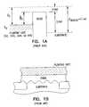
- FIG. 1AOne example of the use of different floating gate ( FIG. 1A ) materials is provided in U.S. Pat. No. 5,801,401 by L. Forbes, entitled “FLASH MEMORY WITH MICROCRYSTALLINE SILICON CARBIDE AS THE FLOATING GATE STRUCTURE.” Another example is provided in U.S. Pat. No. 5,852,306 by L. Forbes, entitled “FLASH MEMORY WITH NANOCRYSTALLINE SILICON FILM AS THE FLOATING GATE.” Still further examples of this approach are provided in pending applications by L. Forbes and K.
- FIG. 1BAn example of the use of the structured surface approach ( FIG. 1B ) is provided in U.S. Pat. No. 5,981,350 by J. Geusic, L. Forbes, and K. Y. Ahn, entitled “DRAM CELLS WITH A STRUCTURE SURFACE USING A SELF STRUCTURED MASK.” Another example is provided in U.S. Pat. No. 6,025,627 by L. Forbes and J. Geusic, entitled “ATOMIC LAYER EXPITAXY GATE INSULATORS AND TEXTURED SURFACES FOR LOW VOLTAGE FLASH MEMORIES.”
- FIG. 1CAn example of the use of amorphous SiC gate insulators ( FIG. 1C ) is provided in U.S. patent application Ser. No. 08/903453 by L. Forbes and K. Ahn, entitled “GATE INSULATOR FOR SILICON INTEGRATED CIRCUIT TECHNOLOGY BY THE CARBURIZATION OF SILICON.”
- graded composition insulatorsto increase the tunneling probability and reduce erase time have been described by the same inventors. (See, L. Forbes and J. M. Eldridge, “GRADED COMPOSITION GATE INSULATORS TO REDUCE TUNNELING BARRIERS IN FLASH MEMORY DEVICES,” application Ser. No. 09/945,514.
- the programmable memory address and decode circuitsshould provide improved flash memory densities while avoiding the large barriers to electron tunneling or hot electron injection presented by the silicon oxide-silicon interface, 3.2 eV, which result in slow write and erase speeds even at very high electric fields.
- programmable memory address and decode circuits with low tunnel tunnel barrier interpoly insulators having a tunnel barrier of approximately 2.0 eVare provided.
- the decoder for a memory deviceincludes a number of address lines and a number of output lines wherein the address lines and the output lines form an array.
- a number of logic cellsare formed at the intersections of output lines and address lines.
- Each of the logic cellsincludes a floating gate transistor which includes a first source/drain region and a second source/drain region separated by a channel region in a substrate.
- a floating gateopposes the channel region and is separated therefrom by a gate oxide.
- a control gateopposing the floating gate. The control gate is separated from the floating gate by the low tunnel barrier intergate insulator.
- the low tunnel barrier intergate insulatorincludes a metal oxide insulator selected from the group consisting of PbO, Al 2 O 3 , Ta 2 O 5 , TiO 2 , ZrO 2 , Nb 2 O 5 and/or a Perovskite oxide tunnel barrier.
- the floating gateincludes a polysilicon floating gate having a metal layer formed thereon in contact with the low tunnel barrier intergate insulator.
- the control gateincludes a polysilicon control gate having a metal layer formed thereon in contact with the low tunnel barrier intergate insulator.
- FIGS. 1A-1Cillustrate a number of previous methods for reducing tunneling barriers in Flash memory.
- FIG. 2illustrates one embodiment of a floating gate transistor, or non-volatile memory cell, according to the teachings of the present invention.
- FIG. 3illustrates another embodiment of a floating gate transistor, or non-volatile memory cell, according to the teachings of the present invention.
- FIG. 4is a perspective view illustrating an array of silicon pillars formed on a substrate as used in one embodiment according to the teachings of the present invention.
- FIGS. 5A-5Eare cross sectional views taken along cut line 5 - 5 from FIG. 4 illustrating a number of floating gate and control gate configurations which are included in the scope of the present invention.
- FIGS. 6A-6Dillustrate a number of address coincidence schemes can be used together with the present invention.
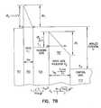
- FIG. 7Ais an energy band diagram illustrating the band structure at vacuum level with the low tunnel barrier interpoly insulator according to the teachings of the present invention.
- FIG. 7Bis an energy band diagram illustrating the band structure during an erase operation of electrons from the floating gate to the control gate across the low tunnel barrier interpoly insulator according to the teachings of the present invention.
- FIG. 7Cis a graph plotting tunneling currents versus the applied electric fields (reciprocal applied electric field shown) for an number of barrier heights.
- FIG. 8shows a conventional NOR decode array for memory circuits according to the teachings of the prior art.
- FIG. 9is a schematic diagram illustrating an embodiment of a decode circuit, or memory address decoder, according to the teachings of the present invention.
- FIG. 10is a simplified block diagram of a high-level organization of an electronic system according to the teachings of the present invention.
- wafer and substrateare interchangeably used to refer generally to any structure on which integrated circuits are formed, and also to such structures during various stages of integrated circuit fabrication. Both terms include doped and undoped semiconductors, epitaxial layers of a semiconductor on a supporting semiconductor or insulating material, combinations of such layers, as well as other such structures that are known in the art.
- doped and undoped semiconductorsinclude doped and undoped semiconductors, epitaxial layers of a semiconductor on a supporting semiconductor or insulating material, combinations of such layers, as well as other such structures that are known in the art.
- horizontalas used in this application is defined as a plane parallel to the conventional plane or surface of a wafer or substrate, regardless of the orientation of the wafer or substrate.
- verticalrefers to a direction perpendicular to the horizonal as defined above.
- Prepositions, such as “on”, “side” (as in “sidewall”), “higher”, “lower”, “over” and “under”are defined with respect to the conventional plane or surface being on the top surface of the wafer or substrate, regardless of the orientation of the wafer or substrate.
- the present inventiondescribes the use of metal oxide inter-poly dielectric insulators between the control gate and the floating gate.
- An exampleis shown in FIG. 2 for a planar structure, or horizontal non-volatile memory cell.
- the use of metal oxide films for this purposeoffer a number of advantages including:
- FIG. 2illustrates one embodiment of a floating gate transistor, or non-volatile memory cell 200 , according to the teachings of the present invention.
- the non-volatile memory cell 200includes a first source/drain region 201 and a second source/drain region 203 separated by a channel region 205 in a substrate 206 .
- a floating gate 209opposes the channel region 205 and is separated therefrom by a gate oxide 211 .
- a control gate 213opposes the floating gate 209 .
- the control gate 213is separated from the floating gate 209 by a low tunnel barrier intergate insulator 215 .
- low tunnel barrier intergate insulator 215includes a metal oxide insulator selected from the group consisting of lead oxide (PbO) and aluminum oxide (Al 2 O 3 ).
- the low tunnel barrier intergate insulator 215includes a transition metal oxide and the transition metal oxide is selected from the group consisting of Ta 2 O 5 , TiO 2 , ZrO 2 , and Nb 2 O 5 .
- the low tunnel barrier intergate insulator 215includes a Perovskite oxide tunnel barrier.
- the floating gate 209includes a polysilicon floating gate 209 having a metal layer 216 formed thereon in contact with the low tunnel barrier intergate insulator 215 .
- the control gate 213includes a polysilicon control gate 213 having a metal layer 217 formed thereon in contact with the low tunnel barrier intergate insulator 215 .
- the metal layers, 216 and 217are formed of the same metal material used to form the metal oxide interpoly insulator 215 .
- FIG. 3illustrates another embodiment of a floating gate transistor, or non-volatile memory cell 300 , according to the teachings of the present invention.
- the non-volatile memory cell 300includes a vertical non volatile memory cell 300 .
- the non-volatile memory cell 300has a first source/drain region 301 formed on a substrate 306 .
- a body region 307 including a channel region 305is formed on the first source/drain region 301 .
- a second source/drain region 303is formed on the body region 307 .
- a floating gate 309opposes the channel region 305 and is separated therefrom by a gate oxide 311 .
- a control gate 313opposes the floating gate 309 . According to the teachings of the present invention, the control gate 313 is separated from the floating gate 309 by a low tunnel barrier intergate insulator 315 .
- the low tunnel barrier intergate insulator 315includes a metal oxide insulator 315 selected from the group consisting of PbO, Al 2 O 3 , Ta 2 O 5 , TiO 2 , ZrO 2 , and Nb 2 O 5 .
- the low tunnel barrier intergate insulator 315includes a Perovskite oxide tunnel barrier.
- the floating gate 309includes a polysilicon floating gate 309 having a metal layer 316 formed thereon in contact with the low tunnel barrier intergate insulator 315 .
- the control gate 313includes a polysilicon control gate 313 having a metal layer 317 formed thereon in contact with the low tunnel barrier intergate insulator 315 .
- the floating gate 309includes a vertical floating gate 309 formed alongside of the body region 307 .
- the control gate 313includes a vertical control gate 313 formed alongside of the vertical floating gate 309 .
- the floating gate 309 and control gate 313 orientation shown in FIG. 3is just one embodiment for a vertical non volatile memory cell 300 , according to the teachings of the present invention.
- the floating gateincludes a horizontally oriented floating gate formed alongside of the body region.
- the control gateincludes a horizontally oriented control gate formed above the horizontally oriented floating gate.
- FIG. 4is a perspective view illustrating an array of silicon pillars 400 - 1 , 400 - 2 , 400 - 3 , . . . , 400 -N, formed on a substrate 406 as used in one embodiment according to the teachings of the present invention.
- the substratescan be (i) conventional p-type bulk silicon or p-type epitaxial layers on p+ wafers, (ii) silicon on insulator formed by conventional SIMOX, wafer bonding and etch back or silicon on sapphire, or (iii) small islands of silicon on insulator utilizing techniques such as described in more detail in U.S. Pat. No. 5,691,230, by Leonard Forbes, entitled “Technique for Producing Small Islands of Silicon on Insulator,” issued Nov. 25, 1997, which is incorporated herein by reference.
- each pillar in the array of silicon pillars 400 - 1 , 400 - 2 , 400 - 3 , . . . , 400 -Nincludes a first source/drain region 401 and a second source/drain region 403 .
- the first and the second source/drain regions, 401 and 403are separated by a body region 407 including channel regions 405 .
- a number of trenches 430separate adjacent pillars in the array of silicon pillars 400 - 1 , 400 - 2 , 400 - 3 , . . . , 400 -N.
- Trenches 430are referenced in connection with the discussion which follows in connection with FIGS. 5A-5E .
- FIGS. 5A-5Eare cross sectional views taken along cut line 5 - 5 from FIG. 4 .
- FIG. 5Aillustrates one such embodiment of the present invention.
- FIG. 5Aillustrates a first source/drain region 501 and second source/drain region 503 for a non-volatile memory cell 500 formed according to the teachings of the present invention.
- the first and second source/drain regions, 501 and 503are contained in a pillar of semiconductor material, and separated by a body region 507 including channel regions 505 .
- FIGS. 5A-5Eare cross sectional views taken along cut line 5 - 5 from FIG. 4 .
- FIG. 5Aillustrates one such embodiment of the present invention.
- FIG. 5Aillustrates a first source/drain region 501 and second source/drain region 503 for a non-volatile memory cell 500 formed according to the teachings of the present invention.
- the first and second source/drain regions, 501 and 503are contained in a pillar of semiconductor
- the first source/drain region 501is integrally connected to a buried sourceline 525 .
- the buried sourceline 525is be formed of semiconductor material which has the same doping type as the first source/drain region 501 .
- the sourceline 525is formed of semiconductor material of the same doping as the first source/drain region 501 , but is more heavily doped than the first source/drain region 501 .
- a pair of floating gates 509 - 1 and 509 - 2are formed in each trench 530 between adjacent pillars which form memory cells 500 - 1 and 500 - 2 .
- Each one of the pair of floating gates, 509 - 1 and 509 - 2respectively opposes the body regions 507 - 1 and 507 - 2 in adjacent pillars 500 - 1 and 500 - 2 on opposing sides of the trench 530 .
- a single control gate 513is shared by the pair of floating gates 509 - 1 and 509 - 2 on opposing sides of the trench 530 .
- the shared single control gate 513can include an integrally formed control gate line.
- an integrally formed control gate line 513can be one of a plurality of control gate lines which are each independently formed in the trench, such as trench 530 , below the top surface of the pillars 500 - 1 and 500 - 2 and between the pair of floating gates 509 - 1 and 509 - 2 .
- each floating gatee.g. 509 - 1 and 509 - 2 , includes a vertically oriented floating gate having a vertical length of less than 100 nanometers.
- a pair of floating gates 509 - 1 and 509 - 2are formed in each trench 530 between adjacent pillars which form memory cells 500 - 1 and 500 - 2 .
- Each one of the pair of floating gates, 509 - 1 and 509 - 2respectively opposes the body regions 507 - 1 and 507 - 2 in adjacent pillars 500 - 1 and 500 - 2 on opposing sides of the trench 530 .
- each trenche.g. 530
- each trenchhouses a pair of control gate lines, shown as 513 - 1 and 513 - 2 .
- Each one of the pair of control gate lines 513 - 1 and 513 - 2addresses the floating gates, 509 - 1 and 509 - 2 respectively, on opposing sides of the trench 530 .
- the pair of control gate lines, or control gates 513 - 1 and 513 - 2are separated by an insulator layer.
- a pair of floating gates 509 - 1 and 509 - 2are again formed in each trench 530 between adjacent pillars which form memory cells 500 - 1 and 500 - 2 .
- Each one of the pair of floating gates, 509 - 1 and 509 - 2respectively opposes the body regions 507 - 1 and 507 - 2 in adjacent pillars 500 - 1 and 500 - 2 on opposing sides of the trench 530 .
- the plurality of control gate linesare disposed vertically above the floating gates. That is, in one embodiment, the control gate lines are located above the pair of floating gates 509 - 1 and 509 - 2 and not fully beneath the top surface of the pillars 500 - 1 and 500 - 2 . In the embodiment of FIG. 5C , each pair of floating gates, e.g. 509 - 1 and 509 - 2 , in a given trench shares a single control gate line, or control gate 513 .
- a pair of floating gates 509 - 1 and 509 - 2are formed in each trench 530 between adjacent pillars which form memory cells 500 - 1 and 500 - 2 .
- Each one of the pair of floating gates, 509 - 1 and 509 - 2respectively opposes the body regions 507 - 1 and 507 - 2 in adjacent pillars 500 - 1 and 500 - 2 on opposing sides of the trench 530 .
- the plurality of control gate linesare disposed vertically above the floating gates. That is, in one embodiment, the control gate lines are located above the pair of floating gates 509 - 1 and 509 - 2 and not fully beneath the top surface of the pillars 500 - 1 and 500 - 2 . However, in the embodiment of FIG. 5D , each one of the pair of floating gates, e.g. 509 - 1 and 509 - 2 , is addressed by an independent one of the plurality of control lines or control gates, shown in FIG. 5D as 513 - 1 and 513 - 2 .
- a single floating gate 509is formed in each trench 530 between adjacent pillars which form memory cells 500 - 1 and 500 - 2 .
- the single floating gate 509can be either a vertically oriented floating gate 509 or a horizontally oriented floating gate 509 formed by conventional processing techniques, or can be a horizontally oriented floating gate 509 formed by a replacement gate technique such as described in a copending application, entitled “Flash Memory with Ultrathin Vertical Body Transistors,” by Leonard Forbes and Kie Y. Ahn, application Ser. No. 09/780,169.
- the floating gate 509has a vertical length facing the body region 505 of less than 100 nm.
- the floating gate 509has a vertical length facing the body region 505 of less than 50 nm.
- the floating gate 509is shared, respectively, with the body regions 507 - 1 and 507 - 2 , including channel regions 505 - 1 and 505 - 2 , in adjacent pillars 500 - 1 and 500 - 2 located on opposing sides of the trench 530 .
- the control gateincludes a single horizontally oriented control gate line, or control gate 513 formed above the horizontally oriented floating gate 509 .
- the floating gates 509are separated from the control gate lines, or control gates 513 with a low tunnel barrier intergate insulator in accordance with the descriptions given above in connection with FIG. 3 .
- the modifications hereare to use tunneling through the interpoly dielectric to realize flash memory devices.
- the vertical devicesinclude an extra flexibility in that the capacitors, e.g. gate oxide and intergate insulator, are easily fabricated with different areas. This readily allows the use of very high dielectric constant inter-poly dielectric insulators with lower tunneling barriers.
- FIGS. 6A-6Cillustrate that a number of address coincidence schemes can be used together with the present invention.
- FIG. 6Aillustrates a NOR flash memory array 610 having a number of non-volatile memory cells 600 - 1 , 600 - 2 , 600 - 3 , using a coincidence address array scheme.
- FIG. 6Ashows a sourceline 625 coupled to a first source/drain region 601 in each of the number of non-volatile memory cells 600 - 1 , 600 - 2 , 600 - 3 .
- the sourcelineis shown oriented in a first selected direction in the flash memory array 610 .
- FIG. 6Aa number of control gate lines 630 are shown oriented in a second selected direction in the flash memory array 610 .
- the number of control gate lines 630are coupled to, or integrally formed with the control gates 613 for the number of non-volatile memory cells 600 - 1 , 600 - 2 , 600 - 3 .
- the second selected directionis orthogonal to the first selected direction.
- FIG. 6Ashows a number of bitlines 635 oriented in a third selected direction in the flash memory array 610 . As shown in FIG.
- the number of bitlinesare coupled to the second source/drain regions 603 in the number of non-volatile memory cells 600 - 1 , 600 - 2 , 600 - 3 .
- the third selected directionis parallel to the second selected direction and the number of control gate lines 630 serve as address lines.
- the flash memory array 610includes a number of backgate or substrate/well bias address lines 640 coupled to the substrate.
- FIGS. 6B-6Cillustrate of top view for three different coincidence address scheme layouts suitable for use with the present invention.
- FIG. 6Bprovides the top view layout of the coincidence address scheme described in connection with FIG. 6A .
- FIG. 6Billustrates a number of sourcelines 625 oriented in a first selected direction, a number of control gate lines 630 oriented in a second selected direction, and a number of bitlines 635 oriented in a third selected direction for the flash memory array 600 .
- the first selected direction and the third selected directionare parallel to one another and orthogonal to the second selected direction.
- the number of control gate lines 630serve as address lines.
- the output lines, e.g. bitlines 635are perpendicular to the address lines, e.g. in this embodiment control gate lines 630 .
- FIG. 6Cprovides the top view layout of yet another coincidence address scheme according to the teachings of the present invention.
- FIG. 6Cillustrates a number of sourcelines 625 oriented in a first selected direction, a number of control gate lines 630 oriented in a second selected direction, and a number of bitlines 635 oriented in a third selected direction for the flash memory array 600 .
- the first selected direction and the second selected directionare parallel to one another and orthogonal to the third selected direction.
- the number of bitlines 635serve as output data lines.
- the sourcelines 625can include a uniform ground plane as the same will be known and understood by one of ordinary skill in the art.
- writecan still be achieved by hot electron injection and/or, according to the teachings of the present invention, tunneling from the control gate.
- block eraseis accomplished by driving the control gates with a relatively large positive voltage and tunneling from the metal on top of the floating gate to the metal on the bottom of the control gate.
- FIG. 7Ais an energy band diagram illustrating the band structure at vacuum level with the low tunnel barrier interpoly insulator according to the teachings of the present invention.
- FIG. 7Ais useful in illustrating the reduced tunnel barrier off of the floating gate to the control gate and for illustrating the respective capacitances of the structure according to the teachings of the present invention.
- FIG. 7Ashows the band structure of the silicon substrate, e.g. channel region 701 , silicon dioxide gate insulator, e.g. gate oxide 703 , polysilicon floating gate 705 , the low tunnel barrier interpoly dielectric 707 , between metal plates 709 and 711 , and then the polysilicon control gate 713 , according to the teachings of the present invention.
- the design considerations involvedare determined by the dielectric constant, thickness and tunneling barrier height of the interpoly dielectric insulator 707 relative to that of the silicon dioxide gate insulator, e.g. gate oxide 703 .
- the tunneling probability through the interpoly dielectric 707is an exponential function of both the barrier height and the electric field across this dielectric.
- FIG. 7Bis an energy band diagram illustrating the band structure during an erase operation of electrons from the floating gate 705 to the control gate 713 across the low tunnel barrier interpoly insulator 707 according to the teachings of the present invention.
- FIG. 7Bis similarly useful in illustrating the reduced tunnel barrier off of the floating gate to the control gate and for illustrating the respective capacitances of the structure according to the teachings of the present invention.
- the electric fieldis determined by the total voltage difference across the structure, the ratio of the capacitances (see FIG. 7A ), and the thickness of the interpoly dielectric 707 .
- the lower electric field in the aluminum oxide interpoly insulator 707 for the same current densityreflects the lower tunneling barrier of less than 2 eV, shown in FIG. 7B , as opposed to the 3.2 eV tunneling barrier of silicon oxide 703 , also illustrated in FIG. 7B .
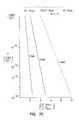
- FIG. 7Cis a graph plotting tunneling currents versus the applied electric fields (reciprocal applied electric field shown) for an number of barrier heights.
- FIG. 7Cillustrates the dependence of the tunneling currents on electric field (reciprocal applied electric field) and barrier height.
- the fraction of voltage across the interpoly or intergate insulator, ⁇ V 2can be increased by making the area of the intergate capacitor, C 2 , (e.g. intergate insulator 707 ) smaller than the area of the transistor gate capacitor, C 1 (e.g. gate oxide 703 ). This would be required with high dielectric constant intergate dielectric insulators 707 and is easily realized with the vertical floating gate structures described above in connection with FIGS. 3 , and 5 A- 5 E.
- the poly-Si layeris to be formed with emphasis on obtaining a surface that is very smooth and morphologically stable at subsequent device processing temperatures which will exceed that used to grow Metal oxide.
- the native SiO x oxide on the poly-Si surfacemust be removed (e.g., by sputter cleaning in an inert gas plasma in situ) just prior to depositing the metal film.
- the electrical characteristics of the resultant Poly-Si/Metal/Metal oxide/Metal/Poly-Si structurewill be better defined and reproducible than that of a Poly-Si/Native SiO x /Metal/Metal oxide/Poly-Si structure.
- the oxide growth rate and limiting thicknesswill increase with oxidation temperature and oxygen pressure.
- the oxidation kinetics of a metalmay, in some cases, depend on the crystallographic orientations of the very small grains of metal which comprise the metal film (see generally, O, Kubaschewski and B. E. Hopkins, “Oxidation of Metals and Alloys”, Butterworth, London, pp. 53-64, 1962). If such effects are significant, the metal deposition process can be modified in order to increase its preferred orientation and subsequent oxide thickness and tunneling uniformity. To this end, use can be made of the fact that metal films strongly prefer to grow during their depositions having their lowest free energy planes parallel to the film surface. This preference varies with the crystal structure of the metal. For example, fcc metals prefer to form ⁇ 111 ⁇ surface plans. Metal orientation effects, if present, would be larger when only a limited fraction of the metal will be oxidized and unimportant when all or most of the metal is oxidized.
- Modifications in the structure shown in FIG. 2may be introduced in order to compensate for certain properties in some metal/oxide/metal layers. Such changes are reasonable since a wide range of metals, alloys and oxides with quite different physical and chemical properties can be used to form these tunnel junctions.
- This oxide barrierhas been studied in detail using Pb/PbO/Pb structures.
- the oxide itselfcan be grown very controllably on deposited lead films using either thermal oxidation (see generally, J. M. Eldridge and J. Matisoo, “Measurement of tunnel current density in a Meal-Oxide-Metal system as a function of oxide thickness,” Proc. 12 th Intern. Conf. on Low Temperature Physics, pp. 427-428, 1971; J. M. Eldridge and D. W. Dong, “Growth of thin PbO layers on lead films. I. Experiment,” Surface Science, Vol. 40, pp. 512-530, 1973) or rf sputter etching in an oxygen plasma (see generally, J.
- Lead and other metal filmscan be deposited by various means including physical sputtering and/or from a Knudsen evaporation cell.
- the sputtering processalso offers the ability to produce smoother films by increasing the re-sputtering-to-deposition ratio since re-sputtering preferentially reduces geometric high points of the film.
- the temperature used to subsequently deposit the Poly-Si control gatemust be held below the melting temperature (327 C) of lead.
- the PbOitself is stable (up to ⁇ 500 C or higher) and thus introduces no temperature constraint on subsequent processes.
- Yet another variation out of severalwould involve: oxidizing the lead film to completion; replacing the top lead electrode with a higher melting metal such as Al; and, then adding the poly-Si control layer. This junction would have asymmetrical tunneling behavior due to the difference in barrier heights between the Pb/PbO and PbO/Al electrodes.
- Tunnel currentsare asymmetrical in this system with somewhat larger currents flowing when electrons are injected from Al/Al 2 O 3 interface developed during oxide growth. This asymmetry is due to a minor change in composition of the growing oxide: there is a small concentration of excess metal in the Al 2 O 3 , the concentration of which diminishes as the oxide is grown thicker. The excess Al +3 ions produce a space charge that lowers the tunnel barrier at the inner interface. The oxide composition at the outer Al 2 O 3 /Al contact is much more stoichiometric and thus has a higher tunnel barrier. In situ ellipsometer measurements on the thermal oxidation of Al films deposited and oxidized in situ support this model (see generally, J. Grimblot and J. M.
- the oxidewill be amorphous and remain so until temperatures in excess of 400 C are reached.
- the initiation of recrystallization and grain growthcan be suppressed, if desired, via the addition of small amounts of glass forming elements (e.g., Si) without altering the growth kinetics or barrier heights significantly.
- Single layers of Ta 2 O 5 , TiO 2 , ZrO 2 , Nb 2 O 5 and similar transition metal oxidescan be formed by “low temperature oxidation” of numerous Transition Metal (e.g., TM oxides) films in molecular and plasma oxygen and also by rf sputtering in an oxygen plasma.
- TM oxidesTransition Metal
- the thermal oxidation kinetics of these metalshave been studied for decades with numerous descriptions and references to be found in the book by Kubaschewski and Hopkins (O. Kubaschewski and B. E. Hopkins, “Oxidation of Metals and Alloys”, Butterworth, London, pp. 53-64, 1962).
- Such metalsoxidize via logarithmic kinetics to reach thicknesses of a few to several tens of angstroms in the range of 100 to 300 C.
- Excellent oxide barriers for Josephson tunnel devicescan be formed by rf sputter etching these metals in an oxygen plasma (see generally, J. M. Greiner, “Josephson tunneling barriers by rf sputter etching in an oxygen plasma,” J. Appl. Phys., Vol. 42, No. 12, pp. 5151-5155, 1971; O. Michikami et al., “Method of fabrication of Josephson tunnel junctions,” U.S. Pat. No. 4,412,902, Nov. 1, 1983).
- Such “low temperature oxidation” approachesdiffer considerably from MOCVD processes used to produce these TM oxides.
- MOCVD filmsrequire high temperature oxidation treatments to remove carbon impurities, improve oxide stoichiometry and produce recrystallization. Such high temperature treatments also cause unwanted interactions between the oxide and the underlying silicon and thus have necessitated the introduction of interfacial barrier layers. See, for example, H. F. Luan et al., “High quality Ta 2 O 5 gate dielectrics with T ox,eq ⁇ 10 angstroms,” IEDM Tech. Digest, pp. 141-144, 1999.
- this treatmentcan be carried out in an inert gas atmosphere, thus lessening the possibility of inadvertently oxidizing the poly-Si floating gate.
- This earlier disclosurewas directed at developing methods and procedures for producing high dielectric constant films for storage cells for DRAMs, the same teachings can be applied to producing thinner metal oxide tunnel films for the flash memory devices described in this disclosure.
- the dielectric constants of these TM oxidesare substantially greater (>25 to 30 or more) than those of PbO and Al 2 O 3 .
- Duplex layers of these high dielectric constant oxide filmsare easily fabricated with simple tools and also provide improvement in device yields and reliability. Each oxide layer will contain some level of defects but the probability that such defects will overlap is exceedingly small.
- Thinner TM layerswill be used in this invention relative to those used to form DRAMs. Unlike DRAMs where leakage must be eliminated, the duplex oxides used here must be thin enough to carry very controlled levels of current flow when subjected to reasonable applied fields and times.
- TM and their oxidesare highly refractory and etchable (e.g., by RIE). Hence they are quite compatible with poly-Si control gate processes and other subsequent steps.
- a stack of oxide filmshaving quite different properties, for example, a stack comprised of a high dielectric constant (k) oxide/a low k oxide/a high k oxide.
- Low temperature oxidationcan be used to form numerous variations of such structures. While most of this disclosure deals with the formation and use of stacks of oxide dielectrics, it is also possible to use “low temperature oxidation” to form other thin film dielectrics such as nitrides, oxynitrides, etc. that could provide additional functions such as being altered by monochromatic light, etc. These will not be discussed further here.
- the dielectric constants of crystallized, perovskite oxidescan be very large, with values in the 100 to 1000 or more range.
- the basic processis more complicated than that needed to oxidize layered films of transition metals.
- the TM layerswould typically be pure metals although they could be alloyed.
- the TMsare similar metallurgically as are their oxides.
- the parent alloy films that can be converted to a perovskite oxideare typically comprised of metals having widely different chemical reactivities with oxygen and other common gasses.
- Y—Ba—Cu system referenced aboveY and Ba are among the most reactive of metals while the reactivity of Cu approaches (albeit distantly) those of other noble metals.
- the alloyis to be completely oxidized, then thin film barriers such as Pd, Pt, etc. or their conductive oxides must be added between the Si and the parent metal film to serve as: electrical contact layers; diffusion barriers; and, oxidation stops.
- the Schottky barrier heights of various TM oxides and perovskite oxides in contact with various metalswill help in the design of the tunnel device.
- the barrier heightswill represent that developed during oxide growth at the parent perovskite alloy/perovskite oxide interface. Obviously, such barrier heights cannot be predicted ab initio for such a wide class of materials but will have to be developed as the need arises. This information will have to be developed on a system-by-system basis.
- Writecan be achieved by the normal channel hot electron injection and gate current through the silicon oxide to the floating gate. This is done by selecting a particular column by applying a high control gate voltage and applying relatively large drain voltage as is done with conventional ETOX flash memory devices.
- writecan also be accomplished by applying a positive voltage to the substrate or well select line and a large negative voltage to the control gates, electrons will tunnel from the control gate to the floating gate.
- the low tunnel barrierwill provide an easy write operation and the selection of the substrate or well bias will provide selectivity and address only one device.
- eraseis achieved by providing a negative voltage to the substrate or well address line and a large positive voltage to the control gate. This causes electrons to tunnel off of the floating gate on to the control gate.
- a whole rowcan be erased by addressing all the column lines along that row and a block can be erased by addressing multiple row back gate or substrate/well address lines.
- Readis accomplished as in conventional ETOX flash memory devices.
- a column lineis addressed by applying a positive control gate voltage and sensing the current along the data bit or drain row address line.
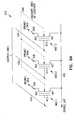
- FIG. 8shows a conventional NOR decode array 800 for memory circuits.
- the address linesare A 1 through A 3 and inverse address lines, ⁇ overscore (A 1 ) ⁇ through ⁇ overscore (A 3 ) ⁇ .
- the conventional NOR decode arrayis programmable at the gate mask level by either fabricating a thin oxide gate transistor, e.g. transistors 801 - 1 , 801 - 2 , . . . , 801 -N, at the intersection of lines in the array or not fabricating a thin oxide gate transistor, e.g. missing thin oxide transistors, 802 - 1 , 802 - 2 , . . . , 802 -N, at such an intersection.
- a thin oxide gate transistore.g. transistors 801 - 1 , 801 - 2 , . . . , 802 -N, at such an intersection.
- NMOS transistors816 are used as load devices.
- each of the row lines 814acts as a NOR gate for the address lines A 1 through A 3 and inverse address lines, ⁇ overscore (A 1 ) ⁇ through ⁇ overscore (A 3 ) ⁇ that are connected to the row lines 814 through the thin oxide gate transistor, e.g. transistors 801 - 1 , 801 - 2 , . . . , 801 -N, of the array. That is, row line R 1 is maintained at a high potential, +VDD, in the positive logic NMOS decode array shown in FIG. 8A , unless one or more of the thin oxide gate transistor, e.g. transistors 801 - 1 , 801 - 2 , . . .
- each thin oxide gate transistore.g. transistors 801 - 1 , 801 - 2 , . . .
- the thin oxide gate transistore.g. transistors 801 - 1 , 801 - 2 , . . . , 801 -N, performs the NOR positive logic circuit function
- an inversion of the OR circuit functionresults from inversion of data onto the row lines 814 through the thin oxide gate transistor, e.g. transistors 801 - 1 , 801 - 2 , . . . , 801 -N, of the array, in order to output a low logic level signal on the row lines 814 .
- a particular row line 814is addressed when none of the thin oxide gate transistor, e.g. transistors 801 - 1 , 801 - 2 , . . . , 801 -N, coupled to that row line 814 are turned “on.”
- the incoming address on each lineis inverted and the combination of the original address and inverted or complemented values used to drive the gates of transistors in the decode array 800 .
- the transistors 801 - 1 , 801 - 2 , . . . , 801 -N in the array 800are enhancement mode NMOS devices and depletion mode NMOS transistors are used as load devices 816 . All voltages are positive in a simple NMOS circuit. This is a positive logic NOR decode array, the logic one state, “1” is the most positive voltage, +VDD, and the logic level zero, “0” is the least positive voltage or ground.
- the transistors used in FIG. 8are NMOS driver transistors with a depletion mode NMOS load technology.
- the load device or NMOS load transistoris a depletion mode or normally “on” transistor which acts as a constant current source during the pull up switching transient thus providing high switching speed.
- the driver transistoris an enhancement mode NMOS transistor which is normally “off” with zero gate bias.
- FIG. 9is a schematic diagram illustrating one embodiment of a decode circuit, or memory address decoder, 900 according to the teachings of the present invention.
- the address linesare A 1 through A 3 and inverse address lines, ⁇ overscore (A 1 ) ⁇ through ⁇ overscore (A 3 ) ⁇ .
- the decode circuit 900is programmable at the gate mask level by either fabricating a driver transistor, or logic cell, e.g. transistors 901 - 1 , 901 - 2 , . . . , 901 -N, at the intersection of lines in the array or not fabricating a driver transistor, or logic cell, e.g.
- fabricating a driver transistore.g. transistors 901 - 1 , 901 - 2 , . . . , 901 -N, at the intersection of lines in the array includes fabricating the floating gate driver transistor according to the embodiments discussed and described in detail in connection with FIGS. 5 and 6 .
- a number of p-channel metal oxide semiconductor (PMOS) load transistors, 916are used as load devices and are coupled to the output lines, or row lines, 914 , of the decode circuit 900 .
- PMOSmetal oxide semiconductor
- the incoming address on each address line A 1 through A 3is inverted and the combination of the original address on each address line A 1 through A 3 and inverted or complemented values on inverse address lines, ⁇ overscore (A 1 ) ⁇ through ⁇ overscore (A 3 ) ⁇ , used to drive the control gates of transistors 901 - 1 , 901 - 2 , . . . , 901 -N in the decode array 900 .
- the floating gate driver transistors, or logic cells, e.g. transistors 901 - 1 , 901 - 2 , . . . , 901 -N in the decode array 900are n-channel floating gate driver transistors having a low tunnel barrier intergate insulator between the control gate and floating gate as described above in connection with FIGS. 5 and 6 .
- each of the row lines 914acts as a NOR gate for the address lines A 1 through A 3 and inverse address lines, ⁇ overscore (A 1 ) ⁇ through ⁇ overscore (A 3 ) ⁇ that are connected to the row lines 914 through the floating gate driver transistors, or logic cells, e.g. transistors 901 - 1 , 901 - 2 , . . . , 901 -N, of the array 900 . That is, row line R 1 is maintained at a high potential VDD, or logic “1” unless one or more of the floating gate driver transistors, or logic cells, e.g. transistors 901 - 1 , 901 - 2 , . . .
- a logic “1”, or VDD, on one of the address lines A 1 through A 3 or inverse address lines, ⁇ overscore (A 1 ) ⁇ through ⁇ overscore (A 3 ) ⁇is required in order to turn on one of the n-channel floating gate driver transistors, or logic cells, e.g. transistors 901 - 1 , 901 - 2 , . . .
- the floating gate driver transistors, or logic cellse.g. transistors 901 - 1 , 901 - 2 , . . . , 901 -N, can be programmed to have two different conductivity states depending upon whether electrons are stored on the floating gate.
- the floating gate transistoris effectively removed from the programmable memory address and decode circuit 900 .
- the driver transistorse.g. transistors 901 - 1 , 901 - 2 , . . . , 901 -N in the array are floating gate transistor devices.
- the floating gate driver transistors 901 - 1 , 901 - 2 , . . . , 901 -Nare formed according to the embodiments of the present invention as disclosed and described in detail in connection with FIGS. 5 and 6 . In this manner, the floating gate driver transistors, 901 - 1 , 901 - 2 , . . .
- the load devices 916shown in the address decoder 900 of FIG. 9 , are p-channel metal oxide semiconductor (PMOS) transistors and not depletion mode n-channel transistors as is more usual.
- PMOSmetal oxide semiconductor
- the decode circuit 900 embodiment of the present invention shown in FIG. 9is formed according to a CMOS process and can be referred to as a CMOS decode array 900 .
- the decode circuit 900 of the present inventionincludes at least one redundant row line, RD.
- a number of additional floating gate driver transistorse.g. transistors T 1 -T 6 , are provided in the array coupled to address lines A 1 through A 3 or inverse address lines, ⁇ overscore (A 1 ) ⁇ through ⁇ overscore (A 3 ) ⁇ and the redundant row line, RD.
- these additional driver transistorse.g. transistors T 1 -T 6 , are formed according to the embodiments described and discussed in detail above in connection with FIGS. 5 and 6 .
- the additional floating gate driver transistors, T 1 -T 6will have a vertical control gate formed by the address lines A 1 through A 3 or inverse address lines, ⁇ overscore (A 1 ) ⁇ through ⁇ overscore (A 3 ) ⁇ .
- the additional floating gate driver transistors, T 1 -T 6will have a horizontal control gate formed by the address lines A 1 through A 3 or inverse address lines, ⁇ overscore (A 1 ) ⁇ through ⁇ overscore (A 3 ) ⁇ located above the floating gates of the floating gate driver transistors, T 1 -T 6 .
- the second source/drain region for the additional driver transistors, T 1 -T 6are coupled to the at least one redundant row line, or wordline, RD.
- a p-channel metal oxide semiconductor (PMOS) load transistor T 7similar to p-channel metal oxide semiconductor (PMOS) load transistors 916 is coupled to the at least one redundant row line, RD as well to complete the CMOS inverter configuration.
- these non volatile, floating gate driver transistorscan be programmed to have two different conductivity states depending upon whether electrons are stored on the vertical floating gate.
- the floating gate transistoris effectively removed from the programmable memory address and decode circuits 900 of the present invention.
- the implementation of these floating gate driver transistors, e.g. transistors T 1 -T 6 , in the decode circuit 900 of the present invention,enables error correction for replacing a row, or column in the array as one of ordinary skill in the art will understand upon reading this disclosure.
- redundant row linese.g. redundant row line RD
- redundant row line RDavailable to replace or error correct for row lines 914 , which are determined defective or which have failed in the field.
- the present inventionis usable to provide such error correction by replacing a row, or column, in a memory decode circuit 900 .
- the floating gate driver transistors, T 1 -T 6have no charge stored on the floating gate they will function as normal inverters for the decode circuit 900 . Conversely, if there is a charge stored charge on the floating gate, the conductivity of the floating gate driver transistors, T 1 -T 6 , will not become high enough and will not function as a driver transistor. In this latter case, the output for the redundant row line RD in the decode circuit 900 of the present invention will not change charge states. Hence, if there is a charge stored on the vertical floating gate of the floating gate driver transistors, T 1 -T 6 , the drivers are effectively removed from the decode circuits 900 .
- the decode circuit shown in FIG. 9can represent a column decode circuit 900 .
- the lines 914 or redundant line RDwhich are coupled to the address lines A 1 through A 3 or inverse address lines, ⁇ overscore (A 1 ) ⁇ through ⁇ overscore (A 3 ) ⁇ through the floating gate driver transistors, 901 - 1 , 901 - 2 , . . . , 901 -N and T 1 -T 6 , can be complementary bit lines for column decoding as the same will be know and understood by one of ordinary skill in the art.
- inverterscan be used as necessary to affect the transition from one logic system, e.g. positive logic system, to a negative logic system while still capitalizing on the utility of the novel floating gate driver transistors 901 - 1 , 901 - 2 , . . . , 901 -N and T 1 -T 6 , having a low tunnel barrier intergate insulator between the control gate and floating gate in decode circuit 900 . If the floating gate in a floating gate driver transistor is programmed with a negative charge on the floating gate it will not be active in the array and it is effectively removed from the array.
- the field programmable, in service or in circuit programmable, logic devices described herework with much lower voltages than the normal devices used in current in field, or in service, programmable decode circuit technology due to tunneling of charge between the floating gate and control gate through the low-tunnel barrier intergate insulator. They can be programmed with Voltages of 2.0 to 4.0 Volts and the normal operating voltages on the vertical control gates can be of the order 1.0 Volt or so.
- the absence of presence of stored charge on the floating gatesis read by addressing the x-address or control gate lines and y-column/sourcelines to form a coincidence in address at a particular floating gate.
- the control gate linewould for instance be driven positive at some voltage of 1.0 Volts and the y-column/sourceline grounded, if the floating gate is not charged with electrons then the floating transistor would turn on tending to hold the row or word address line on that particular row down indicating the presence of a stored “one” in the cell. If this particular floating gate is charged with stored electrons, the transistor will not turn on and the presence of a stored “zero” indicated in the cell. In this manner, data stored on a particular floating gate can be read.
- datais read out in “bit pairs” by addressing not only a single floating gate but rather both of the floating gates in row adjacent pillars on each side of a particular control gate address line.
- Datais stored into the cell by hot electron injection or alternatively, according to the teachings of the present invention, by tunneling charge from the control gate to the floating gate through the low-tunnel barrier intergate insulator. Erasure is accomplished by driving the control gate line with a positive voltage and the sourceline, or backgate/substrate well address line, of the transistor with a negative bias so the total voltage difference is in the order of 2 Volts causing electrons to tunnel off of the floating gates and to the control gates.
- datacan be erased in “bit pairs” since both floating gates on each side of a control gate can be erased at the same time.
- This architectureis amenable to block address schemes where sections of the array are erased and reset at the same time.
- FIG. 10is a simplified block diagram of a high-level organization of an electronic system 1001 according to the teachings of the present invention.
- the electronic system 1001is a system whose functional elements consist of an arithmetic/logic unit (ALU) 1020 or processor 1020 , a control unit 1030 , a memory device unit 1040 and an input/output (I/O) device 1050 .
- ALUarithmetic/logic unit
- processor 1020the electronic system 1001
- control unit 1030the control unit 1030
- memory device unit 1040an input/output
- I/Oinput/output
- Such an electronic system 1001will have a native set of instructions that specify operations to be performed on data by the ALU 1020 and other interactions between the ALU 1020 , the memory device unit 1040 and the I/O devices 1050 .
- the memory device units 1040contain the data plus a stored list of instructions.
- the control unit 1030coordinates all operations of the processor 1020 , the memory device 1040 and the I/O devices 1050 by continuously cycling through a set of operations that cause instructions to be fetched from the memory device 1040 and executed.
- Memory device 1040can be implemented with “in-service” programmable low voltage decode circuits, according to the teachings of the present invention, e.g., having a low-tunnel barrier intergate insulator between the control gate and floating gate.
- the decode circuits of the present inventioncan enable error correction by replacing a row, or column, in a memory array.
- the low tunnel barrier interpoly insulators of the present inventionavoid the large barriers to electron tunneling or hot electron injection presented by the silicon oxide-silicon interface, 3.2 eV, which result in slow write and erase speeds even at very high electric fields.
- the present inventionalso avoids the combination of very high electric fields and damage by hot electron collisions in the which oxide result in a number of operational problems like soft erase error, reliability problems of premature oxide breakdown and a limited number of cycles of write and erase.
- the low tunnel barrier interpoly dielectric insulator erase approach, of the present inventionremedies the above mentioned problems of having a rough top surface on the polysilicon floating gate which results in, poor quality interpoly oxides, sharp points, localized high electric fields, premature breakdown and reliability problems.
- any arbitrary combinational logic functioncan be realized in the so-called sum-of-products form.
- a sum of productsmay be implemented by using a two level logic configuration such as the NOR-NOR arrays shown in FIG. 10 , or by a combination of NOR gates and NAND gates.
- a NAND gatecan be realized by a NOR gate with the inputs inverted.
Landscapes
- Engineering & Computer Science (AREA)
- Microelectronics & Electronic Packaging (AREA)
- Non-Volatile Memory (AREA)
- Semiconductor Memories (AREA)
Abstract
Description
- This application is a divisional of U.S. application Ser. No. 09/945,500 filed Aug. 30, 2001 which is incorporated herein by reference.
- This application is related to the following co-pending, commonly assigned U.S. patent applications: “DRAM Cells with Repressed Memory Metal Oxide Tunnel Insulators,” Ser. No. 09/945,395, “Programmable Array Logic or Memory Devices with Asymmetrical Tunnel Barriers,” Ser. No. 09/943,134, “Dynamic Electrically Alterable Programmable Memory with Insulating Metal Oxide Interpoly Insulators,” Ser. No. 09/945,498, and “Flash Memory with Low Tunnel Barrier Interpoly Insulators,” Ser. No. 09/945,507, “SRAM Cells with Repressed Floating Gate Memory, Metal Oxide Tunnel Interpoly Insulators,” Ser. No. 09/945,554, which are filed on even date herewith and each of which disclosure is herein incorporated by reference.
- The present invention relates generally to integrated circuits, and in particular to in-service programmable logic arrays with low tunnel barrier interpoly insulators.
- Logic circuits are an integral part of digital systems, such as computers. Essentially, a logic circuit processes a number of inputs to produce a number of outputs for use by the digital system. The inputs and outputs are generally electronic signals that take on one of two “binary” values, a “high” logic value or a “low” logic value. The logic circuit manipulates the inputs using binary logic which describes, in a mathematical way, a given or desired relationship between the inputs and the outputs of the logic circuit.
- Logic circuits that are tailored to the specific needs of a particular customer can be very expensive to fabricate on a commercial basis. Thus, general purpose very large scale integration (VLSI) circuits are defined. VLSI circuits serve as many logic roles as possible, which helps to consolidate desired logic functions. However, random logic circuits are still required to tie the various elements of a digital system together.
- Several schemes are used to implement these random logic circuits. One solution is standard logic, such as transistor-transistor logic (TTL). TTL integrated circuits are versatile because they integrate only a relatively small number of commonly used logic functions. The drawback is that large numbers of TTL integrated circuits are typically required for a specific application. This increases the consumption of power and board space, and drives up the overall cost of the digital system.
- One alternative to standard logic is fully custom logic integrated circuits. Custom logic circuits are precisely tailored to the needs of a specific application. This allows the implementation of specific circuit architectures that dramatically reduces the number of parts required for a system. However, custom logic devices require significantly greater engineering time and effort, which increases the cost to develop these circuits and may also delay the production of the end system.
- A less expensive alternative to custom logic is the “programmable logic array.” Programmable logic arrays take advantage of the fact that complex combinational logic functions can be reduced and simplified into various standard forms. For example, logical functions can be manipulated and reduced down to traditional Sum of Products (SOP) form. In SOP form, a logical function uses just two types of logic functions that are implemented sequentially. This-is referred to as two-level logic and can be implemented with various conventional logic functions, e.g., AND-OR, NAND-NAND, NOR-NOR.
- One benefit of the programmable logic array is that it provides a regular, systematic approach to the design of random, combinational logic circuits. A multitude of logical functions can be created from a common building block, e.g., an array of transistors. The logic array is customized or “programmed” by creating a specific metallization pattern to interconnect the various transistors in the array to implement the desired function.
- Programmable logic arrays are fabricated using photolithographic techniques that allow semiconductor and other materials to be manipulated to form integrated circuits as is known in the art. These photolithographic techniques essentially use light that is focused through lenses and masks to define patterns in the materials with microscopic dimensions. The equipment and techniques that are used to implement this photolithography provide a limit for the size of the circuits that can be formed with the materials. Essentially, at some point, the lithography cannot create a fine enough image with sufficient clarity to decrease the size of the elements of the circuit. In other words, there is a minimum dimension that can be achieved through conventional photolithography. This minimum dimension is referred to as the “critical dimension” (CD) or minimum “feature size” (F) of the photolithographic process. The minimum feature size imposes one constraint on the size of the components of a programmable logic array. In order to keep up with the demands for larger programmable logic arrays, designers search for ways to reduce the size of the components of the array.
- As the density requirements become higher and higher in logic and memories it becomes more and more crucial to minimize device area. The programmable logic array (PLA) circuit in the NOR-NOR configuration is one example of an architecture for implementing logic circuits.
- Flash memory cells are one possible solution for high density memory requirements. Flash memories include a single transistor, and with high densities would have the capability of replacing hard disk drive data storage in computer systems. This would result in delicate mechanical systems being replaced by rugged, small and durable solid-state memory packages, and constitute a significant advantage in computer systems. What is required then is a flash memory with the highest possible density or smallest possible cell area.
- Flash memories have become widely accepted in a variety of applications ranging from personal computers, to digital cameras and wireless phones. Both INTEL and AMD have separately each produced about one billion integrated circuit chips in this technology.
- The original EEPROM or EARPROM and flash memory devices described by Toshiba in 1984 used the interploy dielectric insulator for erase. (See generally, F. Masuoka et al., “A new flash EEPROM cell using triple polysilicon technology,” IEEE Int. Electron Devices Meeting, San Francisco, pp. 464-67, 1984; F. Masuoka et al., “256K flash EEPROM using triple polysilicon technology,” IEEE Solid-State Circuits Conf., Philadelphia, pp. 168-169, 1985). Various combinations of silicon oxide and silicon nitride were tried. (See generally, S. Mori et al., “reliable CVD inter-poly dialectics for advanced E&EEPROM,” Symp. On VLSI Technology, Kobe, Japan, pp. 16-17, 1985). However, the rough top surface of the polysilicon floating gate resulted in, poor quality interpoly oxides, sharp points, localized high electric fields, premature breakdown and reliability problems.
- Widespread use of flash memories did not occur until the introduction of the ETOX cell by INTEL in 1988. (See generally, U.S. Pat. No. 4,780,424, “Process for fabricating electrically alterable floating gate memory devices,” 25 Oct. 1988; B. Dipert and L. Hebert, “Flash memory goes mainstream,” IEEE Spectrum, pp. 48-51, October, 1993; R. D. Pashley and S. K. Lai, “Flash memories, the best of two worlds,” IEEE Spectrum, pp. 30-33, December 1989). This extremely simple cell and device structure resulted in high densities, high yield in production and low cost. This enabled the widespread use and application of flash memories anywhere a non-volatile memory function is required. However, in order to enable a reasonable write speed the ETOX cell uses channel hot electron injection, the erase operation which can be slower is achieved by Fowler-Nordhiem tunneling from the floating gate to the source. The large barriers to electron tunneling or hot electron injection presented by the silicon oxide-silicon interface, 3.2 eV, result in slow write and erase speeds even at very high electric fields. The combination of very high electric fields and damage by hot electron collisions in the oxide result in a number of operational problems like soft erase error, reliability problems of premature oxide breakdown and a limited number of cycles of write and erase.
- Other approaches to resolve the above described problems include; the use of different floating gate materials, e.g. SiC, SiOC, GaN, and GaAIN, which exhibit a lower work function (see
FIG. 1A ), the use of structured surfaces which increase the localized electric fields (seeFIG. 1B ), and amorphous SiC gate insulators with larger electron affinity, χ, to increase the tunneling probability and reduce erase time (seeFIG. 1C ). - One example of the use of different floating gate (
FIG. 1A ) materials is provided in U.S. Pat. No. 5,801,401 by L. Forbes, entitled “FLASH MEMORY WITH MICROCRYSTALLINE SILICON CARBIDE AS THE FLOATING GATE STRUCTURE.” Another example is provided in U.S. Pat. No. 5,852,306 by L. Forbes, entitled “FLASH MEMORY WITH NANOCRYSTALLINE SILICON FILM AS THE FLOATING GATE.” Still further examples of this approach are provided in pending applications by L. Forbes and K. Ahn, entitled “DYNAMIC RANDOM ACCESS MEMORY OPERATION OF A FLASH MEMORY DEVICE WITH CHARGE STORAGE ON A LOW ELECTRON AFFINITY GaN OR GaAIN FLOATING GATE,” Ser. No. 08/908098, and “VARIABLE ELECTRON AFFINITY DIAMOND-LIKE COMPOUNDS FOR GATES IN SILICON CMOS MEMORIES AND IMAGING DEVICES,” Ser. No. 08/903452. - An example of the use of the structured surface approach (
FIG. 1B ) is provided in U.S. Pat. No. 5,981,350 by J. Geusic, L. Forbes, and K. Y. Ahn, entitled “DRAM CELLS WITH A STRUCTURE SURFACE USING A SELF STRUCTURED MASK.” Another example is provided in U.S. Pat. No. 6,025,627 by L. Forbes and J. Geusic, entitled “ATOMIC LAYER EXPITAXY GATE INSULATORS AND TEXTURED SURFACES FOR LOW VOLTAGE FLASH MEMORIES.” - Finally, an example of the use of amorphous SiC gate insulators (
FIG. 1C ) is provided in U.S. patent application Ser. No. 08/903453 by L. Forbes and K. Ahn, entitled “GATE INSULATOR FOR SILICON INTEGRATED CIRCUIT TECHNOLOGY BY THE CARBURIZATION OF SILICON.” - Additionally, graded composition insulators to increase the tunneling probability and reduce erase time have been described by the same inventors. (See, L. Forbes and J. M. Eldridge, “GRADED COMPOSITION GATE INSULATORS TO REDUCE TUNNELING BARRIERS IN FLASH MEMORY DEVICES,” application Ser. No. 09/945,514.
- However, all of these approaches relate to increasing tunneling between the floating gate and the substrate such as is employed in a conventional ETOX device and do not involve tunneling between the control gate and floating gate through and inter-poly dielectric.
- Therefore, there is a need in the art to provide improved programmable memory address and decode circuits. The programmable memory address and decode circuits should provide improved flash memory densities while avoiding the large barriers to electron tunneling or hot electron injection presented by the silicon oxide-silicon interface, 3.2 eV, which result in slow write and erase speeds even at very high electric fields. There is also a need to avoid the combination of very high electric fields and damage by hot electron collisions in the which oxide result in a number of operational problems like soft erase error, reliability problems of premature oxide breakdown and a limited number of cycles of write and erase. Further, when using an interpoly dielectric insulator erase approach, the above mentioned problems of having a rough top surface on the polysilicon floating gate which results in, poor quality interpoly oxides, sharp points, localized high electric fields, premature breakdown and reliability problems must be avoided.
- The above mentioned problems with programmable memory address and decode circuits and other problems are addressed by the present invention and will be understood by reading and studying the following specification. Systems and methods are provided for programmable memory address and decode circuits using logic cells, or non-volatile memory cells with metal oxide and/or low tunnel barrier interpoly insulators.
- In one embodiment of the present invention, programmable memory address and decode circuits with low tunnel tunnel barrier interpoly insulators having a tunnel barrier of approximately 2.0 eV are provided. The decoder for a memory device includes a number of address lines and a number of output lines wherein the address lines and the output lines form an array. A number of logic cells are formed at the intersections of output lines and address lines. Each of the logic cells includes a floating gate transistor which includes a first source/drain region and a second source/drain region separated by a channel region in a substrate. A floating gate opposes the channel region and is separated therefrom by a gate oxide. A control gate opposing the floating gate. The control gate is separated from the floating gate by the low tunnel barrier intergate insulator. The low tunnel barrier intergate insulator includes a metal oxide insulator selected from the group consisting of PbO, Al2O3, Ta2O5, TiO2, ZrO2, Nb2O5and/or a Perovskite oxide tunnel barrier. The floating gate includes a polysilicon floating gate having a metal layer formed thereon in contact with the low tunnel barrier intergate insulator. And, the control gate includes a polysilicon control gate having a metal layer formed thereon in contact with the low tunnel barrier intergate insulator.
- These and other embodiments, aspects, advantages, and features of the present invention will be set forth in part in the description which follows, and in part will become apparent to those skilled in the art by reference to the following description of the invention and referenced drawings or by practice of the invention. The aspects, advantages, and features of the invention are realized and attained by means of the instrumentalities, procedures, and combinations particularly pointed out in the appended claims.
FIGS. 1A-1C illustrate a number of previous methods for reducing tunneling barriers in Flash memory.FIG. 2 illustrates one embodiment of a floating gate transistor, or non-volatile memory cell, according to the teachings of the present invention.FIG. 3 illustrates another embodiment of a floating gate transistor, or non-volatile memory cell, according to the teachings of the present invention.FIG. 4 is a perspective view illustrating an array of silicon pillars formed on a substrate as used in one embodiment according to the teachings of the present invention.FIGS. 5A-5E are cross sectional views taken along cut line5-5 fromFIG. 4 illustrating a number of floating gate and control gate configurations which are included in the scope of the present invention.FIGS. 6A-6D illustrate a number of address coincidence schemes can be used together with the present invention.FIG. 7A is an energy band diagram illustrating the band structure at vacuum level with the low tunnel barrier interpoly insulator according to the teachings of the present invention.FIG. 7B is an energy band diagram illustrating the band structure during an erase operation of electrons from the floating gate to the control gate across the low tunnel barrier interpoly insulator according to the teachings of the present invention.FIG. 7C is a graph plotting tunneling currents versus the applied electric fields (reciprocal applied electric field shown) for an number of barrier heights.FIG. 8 shows a conventional NOR decode array for memory circuits according to the teachings of the prior art.FIG. 9 is a schematic diagram illustrating an embodiment of a decode circuit, or memory address decoder, according to the teachings of the present invention.FIG. 10 is a simplified block diagram of a high-level organization of an electronic system according to the teachings of the present invention.- In the following detailed description of the invention, reference is made to the accompanying drawings which form a part hereof, and in which is shown, by way of illustration, specific embodiments in which the invention may be practiced. The embodiments are intended to describe aspects of the invention in sufficient detail to enable those skilled in the art to practice the invention. Other embodiments may be utilized and changes may be made without departing from the scope of the present invention. In the following description, the terms wafer and substrate are interchangeably used to refer generally to any structure on which integrated circuits are formed, and also to such structures during various stages of integrated circuit fabrication. Both terms include doped and undoped semiconductors, epitaxial layers of a semiconductor on a supporting semiconductor or insulating material, combinations of such layers, as well as other such structures that are known in the art. The following detailed description is not to be taken in a limiting sense, and the scope of the present invention is defined only by the appended claims.
- The term “horizontal” as used in this application is defined as a plane parallel to the conventional plane or surface of a wafer or substrate, regardless of the orientation of the wafer or substrate. The term “vertical” refers to a direction perpendicular to the horizonal as defined above. Prepositions, such as “on”, “side” (as in “sidewall”), “higher”, “lower”, “over” and “under” are defined with respect to the conventional plane or surface being on the top surface of the wafer or substrate, regardless of the orientation of the wafer or substrate. The following detailed description is, therefore, not to be taken in a limiting sense, and the scope of the present invention is defined only by the appended claims, along with the full scope of equivalents to which such claims are entitled.
- The present invention, describes the use of metal oxide inter-poly dielectric insulators between the control gate and the floating gate. An example is shown in
FIG. 2 for a planar structure, or horizontal non-volatile memory cell. According to the teachings of the present invention. The use of metal oxide films for this purpose offer a number of advantages including: - (i) Flexibility in selecting a range of smooth metal film surfaces and compositions that can be oxidized to form tunnel barrier insulators.
- (ii) Employing simple “low temperature oxidation” to produce oxide films of highly controlled thickness, composition, purity and uniformity.
- (iii) Avoiding inadvertent inter-diffusion of the metal and silicon as well as silicide formation since the oxidation can be carried out at such low temperatures.
- (iv) Using metal oxides that provide desirably lower tunnel barriers, relative to barriers currently used such as SiO2.
- (v) Providing a wide range of higher dielectric constant oxide films with improved capacitance characteristics.
- (vi) Providing a unique ability to precisely tailor tunnel oxide barrier properties for various device designs and applications.
- (vii) Permitting the use of thicker tunnel barriers, if needed, to enhance device performance and its control along with yield and reliability.
- (viii) Developing layered oxide tunnel barriers by oxidizing layered metal film compositions in order, for example, to enhance device yields and reliability more typical of single insulating layers.
- (ix) Eliminating soft erase errors caused by the current technique of tunnel erase from floating gate to the source.
FIG. 2 illustrates one embodiment of a floating gate transistor, ornon-volatile memory cell 200, according to the teachings of the present invention. As shown inFIG. 2 , thenon-volatile memory cell 200 includes a first source/drain region 201 and a second source/drain region 203 separated by achannel region 205 in asubstrate 206. A floatinggate 209 opposes thechannel region 205 and is separated therefrom by agate oxide 211. Acontrol gate 213 opposes the floatinggate 209. According to the teachings of the present invention, thecontrol gate 213 is separated from the floatinggate 209 by a low tunnelbarrier intergate insulator 215.- In one embodiment of the present invention, low tunnel
barrier intergate insulator 215 includes a metal oxide insulator selected from the group consisting of lead oxide (PbO) and aluminum oxide (Al2O3). In an alternative embodiment of the present invention, the low tunnelbarrier intergate insulator 215 includes a transition metal oxide and the transition metal oxide is selected from the group consisting of Ta2O5, TiO2, ZrO2, and Nb2O5. In still another alternative embodiment of the present invention, the low tunnelbarrier intergate insulator 215 includes a Perovskite oxide tunnel barrier. - According to the teachings of the present invention, the floating
gate 209 includes apolysilicon floating gate 209 having ametal layer 216 formed thereon in contact with the low tunnelbarrier intergate insulator 215. Likewise, thecontrol gate 213 includes apolysilicon control gate 213 having ametal layer 217 formed thereon in contact with the low tunnelbarrier intergate insulator 215. In this invention, the metal layers,216 and217, are formed of the same metal material used to form the metaloxide interpoly insulator 215. FIG. 3 illustrates another embodiment of a floating gate transistor, ornon-volatile memory cell 300, according to the teachings of the present invention. As shown in the embodiment ofFIG. 3 , thenon-volatile memory cell 300 includes a vertical nonvolatile memory cell 300. In this embodiment, thenon-volatile memory cell 300 has a first source/drain region 301 formed on asubstrate 306. Abody region 307 including achannel region 305 is formed on the first source/drain region 301. A second source/drain region 303 is formed on thebody region 307. Methods for forming such a vertical transistor structure are disclosed in U.S. Pat. No. 6,135,175, entitled “Memory Address Decode Array with vertical transistors, which is incorporated herein by reference. A floatinggate 309 opposes thechannel region 305 and is separated therefrom by agate oxide 311. Acontrol gate 313 opposes the floatinggate 309. According to the teachings of the present invention, thecontrol gate 313 is separated from the floatinggate 309 by a low tunnelbarrier intergate insulator 315.- According to the teachings of the present invention, the low tunnel
barrier intergate insulator 315 includes ametal oxide insulator 315 selected from the group consisting of PbO, Al2O3, Ta2O5, TiO2, ZrO2, and Nb2O5. In still another alternative embodiment of the present invention, the low tunnelbarrier intergate insulator 315 includes a Perovskite oxide tunnel barrier. The floatinggate 309 includes apolysilicon floating gate 309 having ametal layer 316 formed thereon in contact with the low tunnelbarrier intergate insulator 315. Thecontrol gate 313 includes apolysilicon control gate 313 having ametal layer 317 formed thereon in contact with the low tunnelbarrier intergate insulator 315. - As shown in
FIG. 3 , the floatinggate 309 includes a vertical floatinggate 309 formed alongside of thebody region 307. In the embodiment shown inFIG. 3 , thecontrol gate 313 includes avertical control gate 313 formed alongside of the vertical floatinggate 309. - As will be explained in more detail below, the floating
gate 309 andcontrol gate 313 orientation shown inFIG. 3 is just one embodiment for a vertical nonvolatile memory cell 300, according to the teachings of the present invention. In other embodiments, explained below, the floating gate includes a horizontally oriented floating gate formed alongside of the body region. In this alternative embodiment, the control gate includes a horizontally oriented control gate formed above the horizontally oriented floating gate. FIG. 4 is a perspective view illustrating an array of silicon pillars400-1,400-2,400-3, . . . ,400-N, formed on asubstrate 406 as used in one embodiment according to the teachings of the present invention. As will be understood by one of ordinary skill in the art upon reading this disclosure, the substrates can be (i) conventional p-type bulk silicon or p-type epitaxial layers on p+ wafers, (ii) silicon on insulator formed by conventional SIMOX, wafer bonding and etch back or silicon on sapphire, or (iii) small islands of silicon on insulator utilizing techniques such as described in more detail in U.S. Pat. No. 5,691,230, by Leonard Forbes, entitled “Technique for Producing Small Islands of Silicon on Insulator,” issued Nov. 25, 1997, which is incorporated herein by reference.- As shown in
FIG. 4 , each pillar in the array of silicon pillars400-1,400-2,400-3, . . . ,400-N, includes a first source/drain region 401 and a second source/drain region 403. The first and the second source/drain regions,401 and403, are separated by abody region 407 includingchannel regions 405. As shown inFIG. 4 , a number oftrenches 430 separate adjacent pillars in the array of silicon pillars400-1,400-2,400-3, . . . ,400-N. Trenches 430 are referenced in connection with the discussion which follows in connection withFIGS. 5A-5E . FIGS. 5A-5E are cross sectional views taken along cut line5-5 fromFIG. 4 . As mentioned above in connection withFIG. 3 , a number of floating gate and control gate configurations are included in the present invention.FIG. 5A illustrates one such embodiment of the present invention.FIG. 5A illustrates a first source/drain region 501 and second source/drain region 503 for a non-volatile memory cell500 formed according to the teachings of the present invention. As shown inFIG. 5 , the first and second source/drain regions,501 and503, are contained in a pillar of semiconductor material, and separated by a body region507 includingchannel regions 505. As shown in the embodiments ofFIGS. 5A-5E , the first source/drain region 501 is integrally connected to a buriedsourceline 525. As one or ordinary skill in the art will understand upon reading this disclosure the buriedsourceline 525 is be formed of semiconductor material which has the same doping type as the first source/drain region 501. In one embodiment, thesourceline 525 is formed of semiconductor material of the same doping as the first source/drain region 501, but is more heavily doped than the first source/drain region 501.- As shown in the embodiment of
FIG. 5A , a pair of floating gates509-1 and509-2 are formed in eachtrench 530 between adjacent pillars which form memory cells500-1 and500-2. Each one of the pair of floating gates,509-1 and509-2, respectively opposes the body regions507-1 and507-2 in adjacent pillars500-1 and500-2 on opposing sides of thetrench 530. - In this embodiment, a
single control gate 513 is shared by the pair of floating gates509-1 and509-2 on opposing sides of thetrench 530. As one of ordinary skill in the art will understand upon reading this disclosure, the sharedsingle control gate 513 can include an integrally formed control gate line. As shown inFIG. 5A , such an integrally formedcontrol gate line 513 can be one of a plurality of control gate lines which are each independently formed in the trench, such astrench 530, below the top surface of the pillars500-1 and500-2 and between the pair of floating gates509-1 and509-2. In one embodiment, according to the teachings of the present invention, each floating gate, e.g.509-1 and509-2, includes a vertically oriented floating gate having a vertical length of less than 100 nanometers. - As shown in the embodiment of
FIG. 5B , a pair of floating gates509-1 and509-2 are formed in eachtrench 530 between adjacent pillars which form memory cells500-1 and500-2. Each one of the pair of floating gates,509-1 and509-2, respectively opposes the body regions507-1 and507-2 in adjacent pillars500-1 and500-2 on opposing sides of thetrench 530. - In the embodiment of
FIG. 5B , a plurality of control gate lines are again formed in trenches,e.g. trench 530, below the top surface of the pillars,500-1 and500-2, and between the pair of floating gates509-1 and509-2. However, in this embodiment, each trench, e.g.530, houses a pair of control gate lines, shown as513-1 and513-2. Each one of the pair of control gate lines513-1 and513-2 adresses the floating gates,509-1 and509-2 respectively, on opposing sides of thetrench 530. In this embodiment, the pair of control gate lines, or control gates513-1 and513-2 are separated by an insulator layer. - As shown in the embodiment of
FIG. 5C , a pair of floating gates509-1 and509-2 are again formed in eachtrench 530 between adjacent pillars which form memory cells500-1 and500-2. Each one of the pair of floating gates,509-1 and509-2, respectively opposes the body regions507-1 and507-2 in adjacent pillars500-1 and500-2 on opposing sides of thetrench 530. - In the embodiment of
FIG. 5C , the plurality of control gate lines are disposed vertically above the floating gates. That is, in one embodiment, the control gate lines are located above the pair of floating gates509-1 and509-2 and not fully beneath the top surface of the pillars500-1 and500-2. In the embodiment ofFIG. 5C , each pair of floating gates, e.g.509-1 and509-2, in a given trench shares a single control gate line, orcontrol gate 513. - As shown in the embodiment of
FIG. 5D , a pair of floating gates509-1 and509-2 are formed in eachtrench 530 between adjacent pillars which form memory cells500-1 and500-2. Each one of the pair of floating gates,509-1 and509-2, respectively opposes the body regions507-1 and507-2 in adjacent pillars500-1 and500-2 on opposing sides of thetrench 530. - In the embodiment of
FIG. 5D , the plurality of control gate lines are disposed vertically above the floating gates. That is, in one embodiment, the control gate lines are located above the pair of floating gates509-1 and509-2 and not fully beneath the top surface of the pillars500-1 and500-2. However, in the embodiment ofFIG. 5D , each one of the pair of floating gates, e.g.509-1 and509-2, is addressed by an independent one of the plurality of control lines or control gates, shown inFIG. 5D as513-1 and513-2. - As shown in the embodiment of
FIG. 5E , a single floatinggate 509 is formed in eachtrench 530 between adjacent pillars which form memory cells500-1 and500-2. According to the teachings of the present invention, the single floatinggate 509 can be either a vertically oriented floatinggate 509 or a horizontally oriented floatinggate 509 formed by conventional processing techniques, or can be a horizontally oriented floatinggate 509 formed by a replacement gate technique such as described in a copending application, entitled “Flash Memory with Ultrathin Vertical Body Transistors,” by Leonard Forbes and Kie Y. Ahn, application Ser. No. 09/780,169. In one embodiment of the present invention, the floatinggate 509 has a vertical length facing thebody region 505 of less than 100 nm. In another embodiment, the floatinggate 509 has a vertical length facing thebody region 505 of less than 50 nm. In one embodiment, as shown inFIG. 5E , the floatinggate 509 is shared, respectively, with the body regions507-1 and507-2, including channel regions505-1 and505-2, in adjacent pillars500-1 and500-2 located on opposing sides of thetrench 530. And, as shown inFIG. 5E , the control gate includes a single horizontally oriented control gate line, orcontrol gate 513 formed above the horizontally oriented floatinggate 509. - As one of ordinary skill in the art will understand upon reading this disclosure, in each of the embodiments described above in connection with
FIGS. 5A-5E the floatinggates 509 are separated from the control gate lines, or controlgates 513 with a low tunnel barrier intergate insulator in accordance with the descriptions given above in connection withFIG. 3 . The modifications here are to use tunneling through the interpoly dielectric to realize flash memory devices. The vertical devices include an extra flexibility in that the capacitors, e.g. gate oxide and intergate insulator, are easily fabricated with different areas. This readily allows the use of very high dielectric constant inter-poly dielectric insulators with lower tunneling barriers. FIGS. 6A-6C illustrate that a number of address coincidence schemes can be used together with the present invention.FIG. 6A illustrates a NORflash memory array 610 having a number of non-volatile memory cells600-1,600-2,600-3, using a coincidence address array scheme. For purposes of illustration,FIG. 6A shows asourceline 625 coupled to a first source/drain region 601 in each of the number of non-volatile memory cells600-1,600-2,600-3. The sourceline is shown oriented in a first selected direction in theflash memory array 610. InFIG. 6A , a number ofcontrol gate lines 630 are shown oriented in a second selected direction in theflash memory array 610. As shown inFIG. 6A , the number ofcontrol gate lines 630 are coupled to, or integrally formed with thecontrol gates 613 for the number of non-volatile memory cells600-1,600-2,600-3. As shown inFIG. 6A , the second selected direction is orthogonal to the first selected direction. Finally,FIG. 6A shows a number ofbitlines 635 oriented in a third selected direction in theflash memory array 610. As shown inFIG. 6A , the number of bitlines are coupled to the second source/drain regions 603 in the number of non-volatile memory cells600-1,600-2,600-3. In the embodiment shown inFIG. 6A the third selected direction is parallel to the second selected direction and the number ofcontrol gate lines 630 serve as address lines. Also, as shown inFIG. 6A , theflash memory array 610 includes a number of backgate or substrate/wellbias address lines 640 coupled to the substrate.- Using
FIG. 6A as a reference point,FIGS. 6B-6C illustrate of top view for three different coincidence address scheme layouts suitable for use with the present invention. First,FIG. 6B provides the top view layout of the coincidence address scheme described in connection withFIG. 6A . This is,FIG. 6B illustrates a number ofsourcelines 625 oriented in a first selected direction, a number ofcontrol gate lines 630 oriented in a second selected direction, and a number ofbitlines 635 oriented in a third selected direction for the flash memory array600. In the embodiment ofFIG. 6B , the first selected direction and the third selected direction are parallel to one another and orthogonal to the second selected direction. In this embodiment, the number ofcontrol gate lines 630 serve as address lines. According to the teachings of the present invention, the output lines, e.g. bitlines635 are perpendicular to the address lines, e.g. in this embodiment control gate lines630. FIG. 6C provides the top view layout of yet another coincidence address scheme according to the teachings of the present invention. This is,FIG. 6C illustrates a number ofsourcelines 625 oriented in a first selected direction, a number ofcontrol gate lines 630 oriented in a second selected direction, and a number ofbitlines 635 oriented in a third selected direction for the flash memory array600. In the embodiment ofFIG. 6C , the first selected direction and the second selected direction are parallel to one another and orthogonal to the third selected direction. In this embodiment, the number ofbitlines 635 serve as output data lines. In an alternative embodiment, thesourcelines 625 can include a uniform ground plane as the same will be known and understood by one of ordinary skill in the art.- As will be apparent to one of ordinary skill in the art upon reading this disclosure, and as will be described in more detail below, write can still be achieved by hot electron injection and/or, according to the teachings of the present invention, tunneling from the control gate. According to the teachings of the present invention, block erase is accomplished by driving the control gates with a relatively large positive voltage and tunneling from the metal on top of the floating gate to the metal on the bottom of the control gate.
FIG. 7A is an energy band diagram illustrating the band structure at vacuum level with the low tunnel barrier interpoly insulator according to the teachings of the present invention.FIG. 7A is useful in illustrating the reduced tunnel barrier off of the floating gate to the control gate and for illustrating the respective capacitances of the structure according to the teachings of the present invention.FIG. 7A shows the band structure of the silicon substrate,e.g. channel region 701, silicon dioxide gate insulator,e.g. gate oxide 703,polysilicon floating gate 705, the low tunnelbarrier interpoly dielectric 707, betweenmetal plates polysilicon control gate 713, according to the teachings of the present invention.- The design considerations involved are determined by the dielectric constant, thickness and tunneling barrier height of the interpoly
dielectric insulator 707 relative to that of the silicon dioxide gate insulator,e.g. gate oxide 703. The tunneling probability through theinterpoly dielectric 707 is an exponential function of both the barrier height and the electric field across this dielectric. FIG. 7B is an energy band diagram illustrating the band structure during an erase operation of electrons from the floatinggate 705 to thecontrol gate 713 across the low tunnelbarrier interpoly insulator 707 according to the teachings of the present invention.FIG. 7B is similarly useful in illustrating the reduced tunnel barrier off of the floating gate to the control gate and for illustrating the respective capacitances of the structure according to the teachings of the present invention.- As shown in
FIG. 7B , the electric field is determined by the total voltage difference across the structure, the ratio of the capacitances (seeFIG. 7A ), and the thickness of theinterpoly dielectric 707. The voltage across theinterpoly dielectric 707 will be, ΔV2=V C 1/(C1+C2), where V is the total applied voltage. The capacitances, C, of the structures depends on the dielectric constant, ∈r, the permittivity of free space, ∈0, and the thickness of the insulating layers, t, and area, A, such that C=∈r∈0A/t, Farads/cm2, where ∈rrepresents the low frequency dielectric constant. The electric field across the interpolydielectric insulator 707, having capacitance, C2, will then be E2=ΔV2/t2, where t2 is the thickness of this layer. - The tunneling current in erasing charge from the floating
gate 705 by tunneling to thecontrol gate 713 will then be as shown inFIG. 7B given by an equation of the form:
J=Bexp(−Eo/E)
where E is the electric field across the interpolydielectric insulator 707 and Eo depends on the barrier height. Practical values of current densities for aluminum oxide which has a current density of 1 A/cm2at a field of about E=1V/20 A=5×10+6V/cm are evidenced in a description by Pollack. (See generally, S. R. Pollack and C. E. Morris, “Tunneling through gaseous oxidized films of Al2O3,” Trans. AIME, Vol. 233, p. 497, 1965). Practical current densities for silicon oxide transistor gate insulators which has a current density of 1 A/cm2at a field of about E=2.3V/23 A=1×10+7V/cm are evidenced in a description by T. P. Ma et al. (See generally, T. P. Ma et al., “Tunneling leakage current in ultrathin (<a4 nm) nitride/oxide stack dielectrics,” IEEE Electron Device Letters, vol. 19, no. 10, pp. 388-390, 1998). - The lower electric field in the aluminum
oxide interpoly insulator 707 for the same current density reflects the lower tunneling barrier of less than 2 eV, shown inFIG. 7B , as opposed to the 3.2 eV tunneling barrier ofsilicon oxide 703, also illustrated inFIG. 7B . FIG. 7C is a graph plotting tunneling currents versus the applied electric fields (reciprocal applied electric field shown) for an number of barrier heights.FIG. 7C illustrates the dependence of the tunneling currents on electric field (reciprocal applied electric field) and barrier height. The fraction of voltage across the interpoly or intergate insulator, ΔV2, can be increased by making the area of the intergate capacitor, C2, (e.g. intergate insulator707) smaller than the area of the transistor gate capacitor, C1 (e.g. gate oxide703). This would be required with high dielectric constant intergatedielectric insulators 707 and is easily realized with the vertical floating gate structures described above in connection withFIGS. 3 , and5A-5E.- Methods of Formation
- Several examples are outlined below in order to illustrate how a diversity of such metal oxide tunnel barriers can be formed, according to the teachings of the present invention. Processing details and precise pathways taken which are not expressly set forth below will be obvious to one of ordinary skill in the art upon reading this disclosure. Firstly, although not included in the details below, it is important also to take into account the following processing factors in connection with the present invention:
- (i) The poly-Si layer is to be formed with emphasis on obtaining a surface that is very smooth and morphologically stable at subsequent device processing temperatures which will exceed that used to grow Metal oxide.
- (ii) The native SiOxoxide on the poly-Si surface must be removed (e.g., by sputter cleaning in an inert gas plasma in situ) just prior to depositing the metal film. The electrical characteristics of the resultant Poly-Si/Metal/Metal oxide/Metal/Poly-Si structure will be better defined and reproducible than that of a Poly-Si/Native SiOx/Metal/Metal oxide/Poly-Si structure.
- (iii) The oxide growth rate and limiting thickness will increase with oxidation temperature and oxygen pressure. The oxidation kinetics of a metal may, in some cases, depend on the crystallographic orientations of the very small grains of metal which comprise the metal film (see generally, O, Kubaschewski and B. E. Hopkins, “Oxidation of Metals and Alloys”, Butterworth, London, pp. 53-64, 1962). If such effects are significant, the metal deposition process can be modified in order to increase its preferred orientation and subsequent oxide thickness and tunneling uniformity. To this end, use can be made of the fact that metal films strongly prefer to grow during their depositions having their lowest free energy planes parallel to the film surface. This preference varies with the crystal structure of the metal. For example, fcc metals prefer to form {111} surface plans. Metal orientation effects, if present, would be larger when only a limited fraction of the metal will be oxidized and unimportant when all or most of the metal is oxidized.
- (iv) Modifications in the structure shown in
FIG. 2 may be introduced in order to compensate for certain properties in some metal/oxide/metal layers. Such changes are reasonable since a wide range of metals, alloys and oxides with quite different physical and chemical properties can be used to form these tunnel junctions. - This oxide barrier has been studied in detail using Pb/PbO/Pb structures. The oxide itself can be grown very controllably on deposited lead films using either thermal oxidation (see generally, J. M. Eldridge and J. Matisoo, “Measurement of tunnel current density in a Meal-Oxide-Metal system as a function of oxide thickness,” Proc. 12thIntern. Conf. on Low Temperature Physics, pp. 427-428, 1971; J. M. Eldridge and D. W. Dong, “Growth of thin PbO layers on lead films. I. Experiment,” Surface Science, Vol. 40, pp. 512-530, 1973) or rf sputter etching in an oxygen plasma (see generally, J. H. Greiner, “Oxidation of lead films by rf sputter etching in an oxygen plasma”, J. Appl. Phys., Vol. 45, No. 1, pp. 32-37, 1974). It will be seen that there are a number of possible variations on this structure. Starting with a clean poly-Si substrate, one processing sequence using thermal oxidation involves:
- (i) Depositing a clean lead film on the poly-Si floating gate at ˜25 to 75 C in a clean vacuum system having a base pressure of ˜10−8Torr or lower. The Pb film will be very thin with a thickness within 1 or 2 A of its target value.
- (ii) Lead and other metal films can be deposited by various means including physical sputtering and/or from a Knudsen evaporation cell. The sputtering process also offers the ability to produce smoother films by increasing the re-sputtering-to-deposition ratio since re-sputtering preferentially reduces geometric high points of the film.
- (iii) Using a “low temperature oxidation process” to grow an oxide film of self-limited thickness. In this case, oxygen gas is introduced at the desired pressure in order to oxidize the lead in situ without an intervening exposure to ambient air. For a fixed oxygen pressure and temperature, the PbO thickness increases with log(time). Its thickness can be controlled via time or other parameters to within 0.10 A, as determined via in situ ellipsometric or ex situ measurements of Josephson tunneling currents. This control is demonstrated by the very limited statistical scatter of the current PbO thickness data shown in the insert of
FIG. 3 in an article by J. M. Eldridge and J. Matisoo, entitled “Measurement of tunnel current density in a Meal-Oxide-Metal system as a function of oxide thickness,” Proc. 12thIntern. Conf. on Low Temperature Physics, pp. 427-428, 1971. This remarkable degree of control over tunnel current is due to the excellent control over PbO thickness that can be achieved by “low temperature oxidation.” For example, increasing the oxidation time from 100 to 1,000 minutes at an oxygen pressure of 750 Torr at 25 C only raises the PbO thickness by 3 A (e.g., from ˜21 to 24 A, seeFIG. 1 in J. M. Eldridge and J. Matisoo, “Measurement of tunnel current density in a Meal-Oxide-Metal system as a function of oxide thickness,” Proc. 12thIntern. Conf. on Low Temperature Physics, pp. 427-428, 1971). Accordingly, controlling the oxidation time to within 1 out of a nominal 100 minute total oxidation time provides a thickness that is within 0.1 A of 21 A. The PbO has a highly stoichiometric composition throughout its thickness, as evidenced from ellipsometry (e.g., seeFIG. 6 in J. M. Eldridge and D. W. Dong, “Growth of thin PbO layers on lead films. I. Experiment,” Surface Science, Vol. 40, pp. 512-530, 1973) and the fact that the tunnel barrier heights are identical for Pb/PbO/Pb structures. - (iv) Re-evacuate the system and deposit the top lead electrode. This produces a tunnel structure having virtually identical tunnel barriers at both Pb/O interfaces.
- (v) The temperature used to subsequently deposit the Poly-Si control gate must be held below the melting temperature (327 C) of lead. The PbO itself is stable (up to ˜500 C or higher) and thus introduces no temperature constraint on subsequent processes. One may optionally oxidize the lead film to completion, thereby circumventing the low melting temperature of metallic lead. In this case, one would form a Poly-Si/PbO/Poly-Si tunnel structure having an altered tunnel barrier for charge injection. Yet another variation out of several would involve: oxidizing the lead film to completion; replacing the top lead electrode with a higher melting metal such as Al; and, then adding the poly-Si control layer. This junction would have asymmetrical tunneling behavior due to the difference in barrier heights between the Pb/PbO and PbO/Al electrodes.
- A number of studies have dealt with electron tunneling in Al/Al2O3/Al structures where the oxide was grown by “low temperature oxidation” in either molecular or plasma oxygen (see generally, S. M. Sze, Physics of Semiconductor Devices, Wiley, N.Y., pp. 553-556, 1981; G. Simmons and A. El-Badry, “Generalized formula for the electric tunnel effect between similar electrodes separated by a thin insulating film,” J. Appl. Phys., Vol. 34, p. 1793, 1963; S. R. Pollack and C. E. Morris, “Tunneling through gaseous oxidized films of Al2O3,” Trans. AIME, Vol. 233, p. 497, 1965; Z. Hurych, “Influence of nonuniform thickness of dielectric layers on capacitance and tunnel currents,” Solid-State Electronics, Vol. 9, p. 967, 1966; S. P. S. Arya and H. P. Singh, “Conduction properties of thin Al2O3films,” Thin Solid Films, Vol. 91, No. 4, pp. 363-374, May 1982; K.-H. Gundlach and J. Holzl, “Logarithmic conductivity of Al—Al2O3—Al tunneling junctions produced by plasma- and by thermal-oxidation”, surface Science, Vol. 27, pp. 125-141, 1971). Before sketching out a processing sequence for these tunnel barriers, note:
- (i) Capacitance and tunnel measurements indicate that the Al2O3thickness increases with the log (oxidation time), similar to that found for PbO/Pb as well as a great many other oxide/metal systems.
- (ii) Tunnel currents are asymmetrical in this system with somewhat larger currents flowing when electrons are injected from Al/Al2O3interface developed during oxide growth. This asymmetry is due to a minor change in composition of the growing oxide: there is a small concentration of excess metal in the Al2O3, the concentration of which diminishes as the oxide is grown thicker. The excess Al+3ions produce a space charge that lowers the tunnel barrier at the inner interface. The oxide composition at the outer Al2O3/Al contact is much more stoichiometric and thus has a higher tunnel barrier. In situ ellipsometer measurements on the thermal oxidation of Al films deposited and oxidized in situ support this model (see generally, J. Grimblot and J. M. Eldridge, “I. Interaction of Al films with O2at low pressures”, J. Electro. Chem. Soc., Vol. 129, No. 10, pp. 2366-2368, 1982. J. Grimblot and J. M. Eldridge, “II. Oxidation of Al films”, ibid, 2369-2372, 1982). In spite of this minor complication, Al/Al2O3/Al tunnel barriers can be formed that will produce predictable and highly controllable tunnel currents that can be ejected from either electrode. The magnitude of the currents are still primarily dominated by Al2O3thickness which can be controlled via the oxidation parametrics.
- With this background, we can proceed to outline one process path out of several that can be used to form Al2O3tunnel barriers. Here the aluminum is thermally oxidized although one could use other techniques such as plasma oxidation (see generally, S. R. Pollack and C. E. Morris, “Tunneling through gaseous oxidized films of Al2O3,” Trans. AIME, Vol. 233, p. 497, 1965; K.-H. Gundlach and J. Holzl, “Logarithmic conductivity of Al—Al2O3—Al tunneling junctions produced by plasma- and by thermal-oxidation”, Surface Science, Vol. 27, pp. 125-141, 1971) or rf sputtering in an oxygen plasma (see generally, J. H. Greiner, “Oxidation of lead films by rf sputter etching in an oxygen plasma”, J. Appl. Phys., Vol. 45, No. 1, pp. 32-37, 1974). For the sake of brevity, some details noted above will not be repeated. The formation of the Al/Al2O3/Al structures will be seen to be simpler than that described for the Pb/PbO/Pb junctions owing to the much higher melting point of aluminum, relative to lead.
- (i) Sputter deposit aluminum on poly-Si at a temperature of ˜25 to 150 C. Due to thermodynamic forces, the micro-crystallites of the f.c.c. aluminum will have a strong and desirable (111) preferred orientation.
- (ii) Oxidize the aluminum in situ in molecular oxygen using temperatures, pressure and time to obtain the desired Al2O3thickness. As with PbO, the thickness increases with log (time) and can be controlled via time at a fixed oxygen pressure and temperature to within 0.10 Angstroms, when averaged over a large number of aluminum grains that are present under the counter-electrode. One can readily change the Al2O3thickness from ˜15 to 35 A by using appropriate oxidation parametrics (e.g., see
FIG. 2 in J. Grimblot and J. M. Eldridge, “II. Oxidation of Al films”, J. Electro. Chem. Soc., Vol. 129, No. 10, pp. 2369-2372, 1982). The oxide will be amorphous and remain so until temperatures in excess of 400 C are reached. The initiation of recrystallization and grain growth can be suppressed, if desired, via the addition of small amounts of glass forming elements (e.g., Si) without altering the growth kinetics or barrier heights significantly. - (iii) Re-evacuate the system and deposit a second layer of aluminum.
- (iv) Deposit the Poly-Si control gate layer using conventional processes.
- Single layers of Ta2O5, TiO2, ZrO2, Nb2O5and similar transition metal oxides can be formed by “low temperature oxidation” of numerous Transition Metal (e.g., TM oxides) films in molecular and plasma oxygen and also by rf sputtering in an oxygen plasma. The thermal oxidation kinetics of these metals have been studied for decades with numerous descriptions and references to be found in the book by Kubaschewski and Hopkins (O. Kubaschewski and B. E. Hopkins, “Oxidation of Metals and Alloys”, Butterworth, London, pp. 53-64, 1962). In essence, such metals oxidize via logarithmic kinetics to reach thicknesses of a few to several tens of angstroms in the range of 100 to 300 C. Excellent oxide barriers for Josephson tunnel devices can be formed by rf sputter etching these metals in an oxygen plasma (see generally, J. M. Greiner, “Josephson tunneling barriers by rf sputter etching in an oxygen plasma,” J. Appl. Phys., Vol. 42, No. 12, pp. 5151-5155, 1971; O. Michikami et al., “Method of fabrication of Josephson tunnel junctions,” U.S. Pat. No. 4,412,902, Nov. 1, 1983). Such “low temperature oxidation” approaches differ considerably from MOCVD processes used to produce these TM oxides. MOCVD films require high temperature oxidation treatments to remove carbon impurities, improve oxide stoichiometry and produce recrystallization. Such high temperature treatments also cause unwanted interactions between the oxide and the underlying silicon and thus have necessitated the introduction of interfacial barrier layers. See, for example, H. F. Luan et al., “High quality Ta2O5gate dielectrics with Tox,eq<10 angstroms,” IEDM Tech. Digest, pp. 141-144, 1999.
- A new approach was described in a copending application by J. M. Eldridge, entitled “Thin Dielectric Films for DRAM Storage Capacitors,” patent application Ser. No. 09/651,380 filed Aug. 29, 2000 that utilizes “low temperature oxidation” to form duplex layers of TM oxides. Unlike MOCVD films, the oxides are very pure and stoichiometric as formed. They do require at least a brief high temperature (est. 700 to 800 C but may be lower) treatment to transform their microstructures from amorphous to crystalline and thus increase their dielectric constants to the desired values (>20 or so). Unlike MOCVD oxides, this treatment can be carried out in an inert gas atmosphere, thus lessening the possibility of inadvertently oxidizing the poly-Si floating gate. While this earlier disclosure was directed at developing methods and procedures for producing high dielectric constant films for storage cells for DRAMs, the same teachings can be applied to producing thinner metal oxide tunnel films for the flash memory devices described in this disclosure. The dielectric constants of these TM oxides are substantially greater (>25 to 30 or more) than those of PbO and Al2O3. Duplex layers of these high dielectric constant oxide films are easily fabricated with simple tools and also provide improvement in device yields and reliability. Each oxide layer will contain some level of defects but the probability that such defects will overlap is exceedingly small. Effects of such duplex layers were first reported by one J. M. Eldridge of the present authors and are well known to practitioners of the art. It is worth mentioning that highly reproducible TM oxide tunnel barriers can be grown by rf sputtering in an oxygen ambient, as referenced above (see generally, J. M. Greiner, “Josephson tunneling barriers by rf sputter etching in an oxygen plasma,” J. Appl. Phys., Vol. 42, No. 12, pp. 5151-5155, 1971; O. Michikami et al., “Method of fabrication of Josephson tunnel junctions,” U.S. Pat. No. 4,412,902, Nov. 1, 1983). Control over oxide thickness and other properties in these studies were all the more remarkable in view of the fact that the oxides were typically grown on thick (e.g., 5,000 A) metals such as Nb and Ta. In such metal-oxide systems, a range of layers and suboxides can also form, each having their own properties. In the present disclosure, control over the properties of the various TM oxides will be even better since we employ very limited (perhaps 10 to 100 A or so) thicknesses of metal and thereby preclude the formation of significant quantities of unwanted, less controllable sub-oxide films. Thermodynamic forces will drive the oxide compositions to their most stable, fully oxidized state, e.g., Nb2O5, Ta2O5, etc. As noted above, it will still be necessary to crystallize these duplex oxide layers. Such treatments can be done by RTP and will be shorter than those used on MOCVD and sputter-deposited oxides since the stoichiometry and purity of the “low temperature oxides” need not be adjusted at high temperature.
- Fairly detailed descriptions for producing thicker duplex layers of TM oxides have been given in the copending application by J. M. Eldridge, entitled “Thin Dielectric Films for DRAM Storage Capacitors,” patent application Ser. No. 09/651,380 filed Aug. 29, 2000, so there is no need to repeat them here. Although perhaps obvious to those skilled in the art, one can sketch out a few useful fabrication guides:
- (i) Thinner TM layers will be used in this invention relative to those used to form DRAMs. Unlike DRAMs where leakage must be eliminated, the duplex oxides used here must be thin enough to carry very controlled levels of current flow when subjected to reasonable applied fields and times.
- (ii) The TM and their oxides are highly refractory and etchable (e.g., by RIE). Hence they are quite compatible with poly-Si control gate processes and other subsequent steps.
- (iii) TM silicide formation will not occur during the oxidation step. It could take place at a significant rate at the temperatures used to deposit the poly-Si control gate. If so, several solutions can be applied including:
- (i) Insert certain metals at the TM/poly-Si boundaries that will prevent inter-diffusion of the TM and the poly-Si.
- (ii) Completely oxide the TMs. The electrical characteristics of the resulting poly-Si/
TM oxide 1/TM oxide 2/poly-Si structure will be different in the absence of having TM at the oxide/metal interfaces.
- Although no applications may be immediately obvious, it is conceivable that one might want to form a stack of oxide films having quite different properties, for example, a stack comprised of a high dielectric constant (k) oxide/a low k oxide/a high k oxide. “Low temperature oxidation” can be used to form numerous variations of such structures. While most of this disclosure deals with the formation and use of stacks of oxide dielectrics, it is also possible to use “low temperature oxidation” to form other thin film dielectrics such as nitrides, oxynitrides, etc. that could provide additional functions such as being altered by monochromatic light, etc. These will not be discussed further here.
- Some results have been obtained which demonstrate that at least a limited range of high temperature, super-conducting oxide films can be made by thermally oxidizing Y—Ba—Cu alloy films (see generally, Hase et al., “Method of manufacturing an oxide superconducting film,” U.S. Pat. No. 5,350,738, Sep. 27, 1994). The present inventors have also disclosed how to employ “low temperature oxidation” and short thermal treatments in an inert ambient at 700 C in order to form a range of perovskite oxide films from parent alloy films (see generally, J. M. Eldridge, “Low Cost Processes for Producing High Quality Perovskite Dielectric Films,” application Ser. No. ______). The dielectric constants of crystallized, perovskite oxides can be very large, with values in the 100 to 1000 or more range. The basic process is more complicated than that needed to oxidize layered films of transition metals. (See Example III.) The TM layers would typically be pure metals although they could be alloyed. The TMs are similar metallurgically as are their oxides. In contrast, the parent alloy films that can be converted to a perovskite oxide are typically comprised of metals having widely different chemical reactivities with oxygen and other common gasses. In the Y—Ba—Cu system referenced above, Y and Ba are among the most reactive of metals while the reactivity of Cu approaches (albeit distantly) those of other noble metals. If the alloy is to be completely oxidized, then thin film barriers such as Pd, Pt, etc. or their conductive oxides must be added between the Si and the parent metal film to serve as: electrical contact layers; diffusion barriers; and, oxidation stops. In such a case, the Schottky barrier heights of various TM oxides and perovskite oxides in contact with various metals will help in the design of the tunnel device. In the more likely event that the perovskite parent alloy film will be only partially converted to oxide and then covered with a second layer of the parent alloy (recall the structure of
FIG. 2 ), then the barrier heights will represent that developed during oxide growth at the parent perovskite alloy/perovskite oxide interface. Obviously, such barrier heights cannot be predicted ab initio for such a wide class of materials but will have to be developed as the need arises. This information will have to be developed on a system-by-system basis. - Methods of Operation
- Write Operation
- Write can be achieved by the normal channel hot electron injection and gate current through the silicon oxide to the floating gate. This is done by selecting a particular column by applying a high control gate voltage and applying relatively large drain voltage as is done with conventional ETOX flash memory devices. However, according to the teachings of the present invention, write can also be accomplished by applying a positive voltage to the substrate or well select line and a large negative voltage to the control gates, electrons will tunnel from the control gate to the floating gate. The low tunnel barrier will provide an easy write operation and the selection of the substrate or well bias will provide selectivity and address only one device.
- Erase Operation
- According to the teachings of the present invention, erase is achieved by providing a negative voltage to the substrate or well address line and a large positive voltage to the control gate. This causes electrons to tunnel off of the floating gate on to the control gate. A whole row can be erased by addressing all the column lines along that row and a block can be erased by addressing multiple row back gate or substrate/well address lines.
- Read Operation
- Read is accomplished as in conventional ETOX flash memory devices. A column line is addressed by applying a positive control gate voltage and sensing the current along the data bit or drain row address line.
- System Level
FIG. 8 shows a conventional NOR decodearray 800 for memory circuits. The address lines are A1 through A3 and inverse address lines, {overscore (A1)} through {overscore (A3)}. The conventional NOR decode array is programmable at the gate mask level by either fabricating a thin oxide gate transistor, e.g. transistors801-1,801-2, . . . ,801-N, at the intersection of lines in the array or not fabricating a thin oxide gate transistor, e.g. missing thin oxide transistors,802-1,802-2, . . . ,802-N, at such an intersection. As one of ordinary skill in the art will understand upon reading this disclosure, the same technique is conventionally used to form other types of decode arrays not shown. As shown inFIG. 8 , a number of depletion mode NMOS transistors,816, are used as load devices.- In this embodiment, each of the
row lines 814 acts as a NOR gate for the address lines A1 through A3 and inverse address lines, {overscore (A1)} through {overscore (A3)} that are connected to therow lines 814 through the thin oxide gate transistor, e.g. transistors801-1,801-2, . . . ,801-N, of the array. That is, row line R1 is maintained at a high potential, +VDD, in the positive logic NMOS decode array shown inFIG. 8A , unless one or more of the thin oxide gate transistor, e.g. transistors801-1,801-2, . . . ,801-N, that are coupled to row line R1 are turned on by a high logic level signal, +VDD, on one of the address lines A1 through A3 or inverse address lines, {overscore (A1)} through {overscore (A3)}. When a transistor gate address is activated, by the high logic level signal, +VDD, through address lines A1 through A3 or inverse address lines, {overscore (A)} through {overscore (A3)}, each thin oxide gate transistor, e.g. transistors801-1,801-2, . . . ,801-N, conducts, or is turned “on.” This conduction of the thin oxide gate transistor, e.g. transistors801-1,801-2, . . . ,801-N, performs the NOR positive logic circuit function, an inversion of the OR circuit function results from inversion of data onto therow lines 814 through the thin oxide gate transistor, e.g. transistors801-1,801-2, . . . ,801-N, of the array, in order to output a low logic level signal on the row lines814. Thus, aparticular row line 814 is addressed when none of the thin oxide gate transistor, e.g. transistors801-1,801-2, . . . ,801-N, coupled to thatrow line 814 are turned “on.” - Again, the incoming address on each line is inverted and the combination of the original address and inverted or complemented values used to drive the gates of transistors in the
decode array 800. The transistors801-1,801-2, . . . ,801-N in thearray 800 are enhancement mode NMOS devices and depletion mode NMOS transistors are used asload devices 816. All voltages are positive in a simple NMOS circuit. This is a positive logic NOR decode array, the logic one state, “1” is the most positive voltage, +VDD, and the logic level zero, “0” is the least positive voltage or ground. - The transistors used in
FIG. 8 are NMOS driver transistors with a depletion mode NMOS load technology. The load device or NMOS load transistor is a depletion mode or normally “on” transistor which acts as a constant current source during the pull up switching transient thus providing high switching speed. The driver transistor is an enhancement mode NMOS transistor which is normally “off” with zero gate bias. FIG. 9 is a schematic diagram illustrating one embodiment of a decode circuit, or memory address decoder,900 according to the teachings of the present invention. Analogous toFIG. 8 , the address lines are A1 through A3 and inverse address lines, {overscore (A1)} through {overscore (A3)}. As shown inFIG. 9 , the decode circuit900 is programmable at the gate mask level by either fabricating a driver transistor, or logic cell, e.g. transistors901-1,901-2, . . . ,901-N, at the intersection of lines in the array or not fabricating a driver transistor, or logic cell, e.g. missing floating gate driver transistors902-1,902-2, . . . ,902-N, at such an intersection. In one embodiment according to the teachings of the present invention, fabricating a driver transistor, e.g. transistors901-1,901-2, . . . ,901-N, at the intersection of lines in the array includes fabricating the floating gate driver transistor according to the embodiments discussed and described in detail in connection withFIGS. 5 and 6 . In one embodiment of the present invention, as shown inFIG. 9 , a number of p-channel metal oxide semiconductor (PMOS) load transistors,916, are used as load devices and are coupled to the output lines, or row lines,914, of the decode circuit900.- The incoming address on each address line A1 through A3 is inverted and the combination of the original address on each address line A1 through A3 and inverted or complemented values on inverse address lines, {overscore (A1)} through {overscore (A3)}, used to drive the control gates of transistors901-1,901-2, . . . ,901-N in the decode array900. The floating gate driver transistors, or logic cells, e.g. transistors901-1,901-2, . . . ,901-N in the decode array900 are n-channel floating gate driver transistors having a low tunnel barrier intergate insulator between the control gate and floating gate as described above in connection with
FIGS. 5 and 6 . - In
FIG. 9 , each of the row lines914 acts as a NOR gate for the address lines A1 through A3 and inverse address lines, {overscore (A1)} through {overscore (A3)} that are connected to the row lines914 through the floating gate driver transistors, or logic cells, e.g. transistors901-1,901-2, . . . ,901-N, of the array900. That is, row line R1 is maintained at a high potential VDD, or logic “1” unless one or more of the floating gate driver transistors, or logic cells, e.g. transistors901-1,901-2, . . . ,901-N, that are coupled to row line R1 are turned on by a high logic level signal, VDD, on one of the address lines A1 through A3 or inverse address lines, {overscore (A1)} through {overscore (A3)}. In the decode circuit900 configuration shown inFIG. 9 , a logic “1”, or VDD, on one of the address lines A1 through A3 or inverse address lines, {overscore (A1)} through {overscore (A3)}, is required in order to turn on one of the n-channel floating gate driver transistors, or logic cells, e.g. transistors901-1,901-2, . . . ,901-N, coupled to row line R1. As one of ordinary skill in the art will understand upon reading this disclosure, the floating gate driver transistors, or logic cells, e.g. transistors901-1,901-2, . . . ,901-N, can be programmed to have two different conductivity states depending upon whether electrons are stored on the floating gate. When a charge is stored on the floating gate for any one of these floating gate driver transistors,901-1,901-2, . . . ,901-N, the floating gate transistor is effectively removed from the programmable memory address and decode circuit900. - For the decode circuit900 of the present invention, shown in
FIG. 9 , the driver transistors, e.g. transistors901-1,901-2, . . . ,901-N in the array are floating gate transistor devices. In one embodiment, the floating gate driver transistors901-1,901-2, . . . ,901-N are formed according to the embodiments of the present invention as disclosed and described in detail in connection withFIGS. 5 and 6 . In this manner, the floating gate driver transistors,901-1,901-2, . . . ,901-N, can be programmed initially in fabrication and can be reprogrammed as necessary once the decode array is in service, e.g. field programmable, to implement a specific decode function. The load devices916, shown in the address decoder900 ofFIG. 9 , are p-channel metal oxide semiconductor (PMOS) transistors and not depletion mode n-channel transistors as is more usual. In this manner, the decode circuit900 embodiment of the present invention shown inFIG. 9 is formed according to a CMOS process and can be referred to as a CMOS decode array900. - In one embodiment, as shown in
FIG. 9 , the decode circuit900 of the present invention includes at least one redundant row line, RD. In the embodiment shown inFIG. 9 , a number of additional floating gate driver transistors, e.g. transistors T1-T6, are provided in the array coupled to address lines A1 through A3 or inverse address lines, {overscore (A1)} through {overscore (A3)} and the redundant row line, RD. According to the teachings of the present invention, these additional driver transistors, e.g. transistors T1-T6, are formed according to the embodiments described and discussed in detail above in connection withFIGS. 5 and 6 . In one embodiment, as described above according to the teachings of the present invention, the additional floating gate driver transistors, T1-T6, will have a vertical control gate formed by the address lines A1 through A3 or inverse address lines, {overscore (A1)} through {overscore (A3)}. In another embodiment, as described above according to the teachings of the present invention, the additional floating gate driver transistors, T1-T6, will have a horizontal control gate formed by the address lines A1 through A3 or inverse address lines, {overscore (A1)} through {overscore (A3)} located above the floating gates of the floating gate driver transistors, T1-T6. According to the teachings of the present invention, the second source/drain region for the additional driver transistors, T1-T6, are coupled to the at least one redundant row line, or wordline, RD. A p-channel metal oxide semiconductor (PMOS) load transistor T7, similar to p-channel metal oxide semiconductor (PMOS) load transistors916 is coupled to the at least one redundant row line, RD as well to complete the CMOS inverter configuration. - As has been shown and described above, these non volatile, floating gate driver transistors, e.g. transistors T1-T6, can be programmed to have two different conductivity states depending upon whether electrons are stored on the vertical floating gate. When a charge is stored on the floating gate for any one of these floating gate driver transistors, e.g. transistors T1-T6, the floating gate transistor is effectively removed from the programmable memory address and decode circuits900 of the present invention. The implementation of these floating gate driver transistors, e.g. transistors T1-T6, in the decode circuit900 of the present invention, enables error correction for replacing a row, or column in the array as one of ordinary skill in the art will understand upon reading this disclosure.
- According to the teachings of the present invention, it is desirable to have redundant row lines, e.g. redundant row line RD, available to replace or error correct for row lines914, which are determined defective or which have failed in the field. The present invention is usable to provide such error correction by replacing a row, or column, in a memory decode circuit900.
- One of ordinary skill in the art will understand upon reading this disclosure that there can be more than one redundant row line, e.g. a RD2, RD3, etc. (not shown), and similarly more additional floating gate driver transistors, like transistors TI-T6, coupled thereto in order to enable multiple row error correction. One of ordinary skill in the art will further understand, upon reading this disclosure, the manner in which the additional floating gate driver transistors, T1-T6, formed according to the teachings of the present invention, can be selectively programmed in order to access, or select, redundant rows RD in replacement for any one of the output lines914 in the decode array900.
- In summary, If electrons are stored on a floating gate for one of the additional floating gate driver transistors, T1-T6, then when a high input signal is received on address lines A1 through A3 or inverse address lines, {overscore (A1)} through {overscore (A3)}, the “programmed floating gate driver transistor, T1-T6, will remain “off.” On the other hand, if there is no stored charge on the vertical floating gate for that particular floating gate driver transistors, T1-T6, then the floating gate driver transistors, T1-T6, will conduct when a high input signal is received on address lines A1 through A3 or inverse address lines, {overscore (A1)} through {overscore (A3)} associated with that floating gate driver transistor. If the floating gate driver transistors, T1-T6, have no charge stored on the floating gate they will function as normal inverters for the decode circuit900. Conversely, if there is a charge stored charge on the floating gate, the conductivity of the floating gate driver transistors, T1-T6, will not become high enough and will not function as a driver transistor. In this latter case, the output for the redundant row line RD in the decode circuit900 of the present invention will not change charge states. Hence, if there is a charge stored on the vertical floating gate of the floating gate driver transistors, T1-T6, the drivers are effectively removed from the decode circuits900.
- Analogously, the decode circuit shown in
FIG. 9 can represent a column decode circuit900. In this case, the lines914 or redundant line RD which are coupled to the address lines A1 through A3 or inverse address lines, {overscore (A1)} through {overscore (A3)} through the floating gate driver transistors,901-1,901-2, . . . ,901-N and T1-T6, can be complementary bit lines for column decoding as the same will be know and understood by one of ordinary skill in the art. - As one of ordinary skill in the art will further understand upon reading this disclosure, additional inverters can be used as necessary to affect the transition from one logic system, e.g. positive logic system, to a negative logic system while still capitalizing on the utility of the novel floating gate driver transistors901-1,901-2, . . . ,901-N and T1-T6, having a low tunnel barrier intergate insulator between the control gate and floating gate in decode circuit900. If the floating gate in a floating gate driver transistor is programmed with a negative charge on the floating gate it will not be active in the array and it is effectively removed from the array. In this manner the array logic functions can be programmed even when the circuit is in the final circuit or in the field and being used in a system. The field programmable, in service or in circuit programmable, logic devices described here work with much lower voltages than the normal devices used in current in field, or in service, programmable decode circuit technology due to tunneling of charge between the floating gate and control gate through the low-tunnel barrier intergate insulator. They can be programmed with Voltages of 2.0 to 4.0 Volts and the normal operating voltages on the vertical control gates can be of the order 1.0 Volt or so.
- The absence of presence of stored charge on the floating gates is read by addressing the x-address or control gate lines and y-column/sourcelines to form a coincidence in address at a particular floating gate. The control gate line would for instance be driven positive at some voltage of 1.0 Volts and the y-column/sourceline grounded, if the floating gate is not charged with electrons then the floating transistor would turn on tending to hold the row or word address line on that particular row down indicating the presence of a stored “one” in the cell. If this particular floating gate is charged with stored electrons, the transistor will not turn on and the presence of a stored “zero” indicated in the cell. In this manner, data stored on a particular floating gate can be read. In reality, data is read out in “bit pairs” by addressing not only a single floating gate but rather both of the floating gates in row adjacent pillars on each side of a particular control gate address line. Data is stored into the cell by hot electron injection or alternatively, according to the teachings of the present invention, by tunneling charge from the control gate to the floating gate through the low-tunnel barrier intergate insulator. Erasure is accomplished by driving the control gate line with a positive voltage and the sourceline, or backgate/substrate well address line, of the transistor with a negative bias so the total voltage difference is in the order of 2 Volts causing electrons to tunnel off of the floating gates and to the control gates. According to the teachings of the present invention, data can be erased in “bit pairs” since both floating gates on each side of a control gate can be erased at the same time. This architecture is amenable to block address schemes where sections of the array are erased and reset at the same time.
FIG. 10 is a simplified block diagram of a high-level organization of anelectronic system 1001 according to the teachings of the present invention. As shown inFIG. 10 , theelectronic system 1001 is a system whose functional elements consist of an arithmetic/logic unit (ALU)1020 orprocessor 1020, a control unit1030, amemory device unit 1040 and an input/output (I/O)device 1050. Generally such anelectronic system 1001 will have a native set of instructions that specify operations to be performed on data by theALU 1020 and other interactions between theALU 1020, thememory device unit 1040 and the I/O devices 1050. Thememory device units 1040 contain the data plus a stored list of instructions.- The control unit1030 coordinates all operations of the
processor 1020, thememory device 1040 and the I/O devices 1050 by continuously cycling through a set of operations that cause instructions to be fetched from thememory device 1040 and executed.Memory device 1040 can be implemented with “in-service” programmable low voltage decode circuits, according to the teachings of the present invention, e.g., having a low-tunnel barrier intergate insulator between the control gate and floating gate. In addition, the decode circuits of the present invention can enable error correction by replacing a row, or column, in a memory array. - The above structures and fabrication methods have been described, by way of example and not by way of limitation, with respect to in service programmable logic arrays using non-volatile memory cells with low tunnel barrier interpoly insulators.
- It has been shown that the low tunnel barrier interpoly insulators of the present invention avoid the large barriers to electron tunneling or hot electron injection presented by the silicon oxide-silicon interface, 3.2 eV, which result in slow write and erase speeds even at very high electric fields. The present invention also avoids the combination of very high electric fields and damage by hot electron collisions in the which oxide result in a number of operational problems like soft erase error, reliability problems of premature oxide breakdown and a limited number of cycles of write and erase. Further, the low tunnel barrier interpoly dielectric insulator erase approach, of the present invention remedies the above mentioned problems of having a rough top surface on the polysilicon floating gate which results in, poor quality interpoly oxides, sharp points, localized high electric fields, premature breakdown and reliability problems.
- According to the teachings of the present invention, any arbitrary combinational logic function can be realized in the so-called sum-of-products form. A sum of products may be implemented by using a two level logic configuration such as the NOR-NOR arrays shown in
FIG. 10 , or by a combination of NOR gates and NAND gates. A NAND gate can be realized by a NOR gate with the inputs inverted. By programming the floating gates of the non-volatile memory cells in the array, these arrays can be field programmed or erased and re-programmed to accomplish the required logic functions.
Claims (76)
Priority Applications (1)
| Application Number | Priority Date | Filing Date | Title |
|---|---|---|---|
| US10/931,711US7187587B2 (en) | 2001-08-30 | 2004-09-01 | Programmable memory address and decode circuits with low tunnel barrier interpoly insulators |
Applications Claiming Priority (2)
| Application Number | Priority Date | Filing Date | Title |
|---|---|---|---|
| US09/945,500US7075829B2 (en) | 2001-08-30 | 2001-08-30 | Programmable memory address and decode circuits with low tunnel barrier interpoly insulators |
| US10/931,711US7187587B2 (en) | 2001-08-30 | 2004-09-01 | Programmable memory address and decode circuits with low tunnel barrier interpoly insulators |
Related Parent Applications (1)
| Application Number | Title | Priority Date | Filing Date |
|---|---|---|---|
| US09/945,500DivisionUS7075829B2 (en) | 2001-08-30 | 2001-08-30 | Programmable memory address and decode circuits with low tunnel barrier interpoly insulators |
Publications (2)
| Publication Number | Publication Date |
|---|---|
| US20050024945A1true US20050024945A1 (en) | 2005-02-03 |
| US7187587B2 US7187587B2 (en) | 2007-03-06 |
Family
ID=25483184
Family Applications (2)
| Application Number | Title | Priority Date | Filing Date |
|---|---|---|---|
| US09/945,500Expired - Fee RelatedUS7075829B2 (en) | 2001-08-30 | 2001-08-30 | Programmable memory address and decode circuits with low tunnel barrier interpoly insulators |
| US10/931,711Expired - LifetimeUS7187587B2 (en) | 2001-08-30 | 2004-09-01 | Programmable memory address and decode circuits with low tunnel barrier interpoly insulators |
Family Applications Before (1)
| Application Number | Title | Priority Date | Filing Date |
|---|---|---|---|
| US09/945,500Expired - Fee RelatedUS7075829B2 (en) | 2001-08-30 | 2001-08-30 | Programmable memory address and decode circuits with low tunnel barrier interpoly insulators |
Country Status (1)
| Country | Link |
|---|---|
| US (2) | US7075829B2 (en) |
Cited By (17)
| Publication number | Priority date | Publication date | Assignee | Title |
|---|---|---|---|---|
| US20030045082A1 (en)* | 2001-08-30 | 2003-03-06 | Micron Technology, Inc. | Atomic layer deposition of metal oxide and/or low asymmetrical tunnel barrier interploy insulators |
| US20030048666A1 (en)* | 2001-08-30 | 2003-03-13 | Micron Technology, Inc. | Graded composition metal oxide tunnel barrier interpoly insulators |
| US20040160830A1 (en)* | 2001-08-30 | 2004-08-19 | Micron Technology, Inc. | DRAM cells with repressed floating gate memory, low tunnel barrier interpoly insulators |
| US20040168145A1 (en)* | 2001-08-30 | 2004-08-26 | Micron Technology, Inc. | Service programmable logic arrays with low tunnel barrier interpoly insulators |
| US20050026349A1 (en)* | 2001-08-30 | 2005-02-03 | Micron Technology, Inc. | Flash memory with low tunnel barrier interpoly insulators |
| US20050169054A1 (en)* | 2001-08-30 | 2005-08-04 | Micron Technology, Inc. | SRAM cells with repressed floating gate memory, low tunnel barrier interpoly insulators |
| US20060186458A1 (en)* | 2005-02-23 | 2006-08-24 | Micron Technology,Inc. | Germanium-silicon-carbide floating gates in memories |
| US20070173202A1 (en)* | 2006-01-11 | 2007-07-26 | Serconet Ltd. | Apparatus and method for frequency shifting of a wireless signal and systems using frequency shifting |
| US20080316828A1 (en)* | 2007-06-21 | 2008-12-25 | Hanafi Hussein I | Memory in logic cell |
| US8175649B2 (en) | 2008-06-20 | 2012-05-08 | Corning Mobileaccess Ltd | Method and system for real time control of an active antenna over a distributed antenna system |
| US8325759B2 (en) | 2004-05-06 | 2012-12-04 | Corning Mobileaccess Ltd | System and method for carrying a wireless based signal over wiring |
| US8501563B2 (en) | 2005-07-20 | 2013-08-06 | Micron Technology, Inc. | Devices with nanocrystals and methods of formation |
| US8594133B2 (en) | 2007-10-22 | 2013-11-26 | Corning Mobileaccess Ltd. | Communication system using low bandwidth wires |
| US8897215B2 (en) | 2009-02-08 | 2014-11-25 | Corning Optical Communications Wireless Ltd | Communication system using cables carrying ethernet signals |
| US9184960B1 (en) | 2014-09-25 | 2015-11-10 | Corning Optical Communications Wireless Ltd | Frequency shifting a communications signal(s) in a multi-frequency distributed antenna system (DAS) to avoid or reduce frequency interference |
| US9338823B2 (en) | 2012-03-23 | 2016-05-10 | Corning Optical Communications Wireless Ltd | Radio-frequency integrated circuit (RFIC) chip(s) for providing distributed antenna system functionalities, and related components, systems, and methods |
| US11049807B2 (en) | 2019-09-25 | 2021-06-29 | Sandisk Technologies Llc | Three-dimensional memory device containing tubular blocking dielectric spacers |
Families Citing this family (33)
| Publication number | Priority date | Publication date | Assignee | Title |
|---|---|---|---|---|
| US6744094B2 (en) | 2001-08-24 | 2004-06-01 | Micron Technology Inc. | Floating gate transistor with horizontal gate layers stacked next to vertical body |
| US7012297B2 (en)* | 2001-08-30 | 2006-03-14 | Micron Technology, Inc. | Scalable flash/NV structures and devices with extended endurance |
| US7075829B2 (en)* | 2001-08-30 | 2006-07-11 | Micron Technology, Inc. | Programmable memory address and decode circuits with low tunnel barrier interpoly insulators |
| US6784480B2 (en)* | 2002-02-12 | 2004-08-31 | Micron Technology, Inc. | Asymmetric band-gap engineered nonvolatile memory device |
| US7589029B2 (en) | 2002-05-02 | 2009-09-15 | Micron Technology, Inc. | Atomic layer deposition and conversion |
| US7160577B2 (en) | 2002-05-02 | 2007-01-09 | Micron Technology, Inc. | Methods for atomic-layer deposition of aluminum oxides in integrated circuits |
| US7135421B2 (en) | 2002-06-05 | 2006-11-14 | Micron Technology, Inc. | Atomic layer-deposited hafnium aluminum oxide |
| US7221586B2 (en) | 2002-07-08 | 2007-05-22 | Micron Technology, Inc. | Memory utilizing oxide nanolaminates |
| US7192892B2 (en)* | 2003-03-04 | 2007-03-20 | Micron Technology, Inc. | Atomic layer deposited dielectric layers |
| US7135369B2 (en) | 2003-03-31 | 2006-11-14 | Micron Technology, Inc. | Atomic layer deposited ZrAlxOy dielectric layers including Zr4AlO9 |
| US7081421B2 (en) | 2004-08-26 | 2006-07-25 | Micron Technology, Inc. | Lanthanide oxide dielectric layer |
| US7588988B2 (en) | 2004-08-31 | 2009-09-15 | Micron Technology, Inc. | Method of forming apparatus having oxide films formed using atomic layer deposition |
| US7560395B2 (en) | 2005-01-05 | 2009-07-14 | Micron Technology, Inc. | Atomic layer deposited hafnium tantalum oxide dielectrics |
| US7687409B2 (en) | 2005-03-29 | 2010-03-30 | Micron Technology, Inc. | Atomic layer deposited titanium silicon oxide films |
| US7279740B2 (en) | 2005-05-12 | 2007-10-09 | Micron Technology, Inc. | Band-engineered multi-gated non-volatile memory device with enhanced attributes |
| US7572695B2 (en) | 2005-05-27 | 2009-08-11 | Micron Technology, Inc. | Hafnium titanium oxide films |
| US7402850B2 (en)* | 2005-06-21 | 2008-07-22 | Micron Technology, Inc. | Back-side trapped non-volatile memory device |
| US7829938B2 (en)* | 2005-07-14 | 2010-11-09 | Micron Technology, Inc. | High density NAND non-volatile memory device |
| US7575978B2 (en) | 2005-08-04 | 2009-08-18 | Micron Technology, Inc. | Method for making conductive nanoparticle charge storage element |
| US7989290B2 (en) | 2005-08-04 | 2011-08-02 | Micron Technology, Inc. | Methods for forming rhodium-based charge traps and apparatus including rhodium-based charge traps |
| US8110469B2 (en) | 2005-08-30 | 2012-02-07 | Micron Technology, Inc. | Graded dielectric layers |
| US7629641B2 (en)* | 2005-08-31 | 2009-12-08 | Micron Technology, Inc. | Band engineered nano-crystal non-volatile memory device utilizing enhanced gate injection |
| US7410910B2 (en) | 2005-08-31 | 2008-08-12 | Micron Technology, Inc. | Lanthanum aluminum oxynitride dielectric films |
| US7429767B2 (en)* | 2005-09-01 | 2008-09-30 | Micron Technology, Inc. | High performance multi-level non-volatile memory device |
| US7615385B2 (en) | 2006-09-20 | 2009-11-10 | Hypres, Inc | Double-masking technique for increasing fabrication yield in superconducting electronics |
| US8097912B2 (en)* | 2007-06-13 | 2012-01-17 | Macronix International Co. Ltd. | Systems and methods for self convergence during erase of a non-volatile memory device |
| US7973357B2 (en)* | 2007-12-20 | 2011-07-05 | Samsung Electronics Co., Ltd. | Non-volatile memory devices |
| US7728392B2 (en)* | 2008-01-03 | 2010-06-01 | International Business Machines Corporation | SRAM device structure including same band gap transistors having gate stacks with high-K dielectrics and same work function |
| US8237457B2 (en) | 2009-07-15 | 2012-08-07 | International Business Machines Corporation | Replacement-gate-compatible programmable electrical antifuse |
| US8301214B1 (en) | 2010-01-08 | 2012-10-30 | Hypres, Inc. | System and method for providing multi-conductive layer metallic interconnects for superconducting integrated circuits |
| US8829592B2 (en)* | 2010-12-14 | 2014-09-09 | Intel Corporation | Non-volatile storage element having dual work-function electrodes |
| JP6753450B2 (en)* | 2018-11-12 | 2020-09-09 | セイコーエプソン株式会社 | Substrates for electro-optical devices, electro-optic devices, electronic devices |
| JP7525405B2 (en)* | 2019-01-25 | 2024-07-30 | 株式会社半導体エネルギー研究所 | Semiconductor Device |
Citations (85)
| Publication number | Priority date | Publication date | Assignee | Title |
|---|---|---|---|---|
| US3641084A (en)* | 1969-05-05 | 1972-02-08 | Ethyl Corp | Vinylic aluminacycloalkane compounds and their preparation |
| US3978577A (en)* | 1975-06-30 | 1976-09-07 | International Business Machines Corporation | Fixed and variable threshold N-channel MNOSFET integration technique |
| US4449205A (en)* | 1982-02-19 | 1984-05-15 | International Business Machines Corp. | Dynamic RAM with non-volatile back-up storage and method of operation thereof |
| US4495219A (en)* | 1981-10-09 | 1985-01-22 | Fujitsu Limited | Process for producing dielectric layers for semiconductor devices |
| US4510584A (en)* | 1982-12-29 | 1985-04-09 | Mostek Corporation | MOS Random access memory cell with nonvolatile storage |
| US4665417A (en)* | 1984-09-27 | 1987-05-12 | International Business Machines Corporation | Non-volatile dynamic random access memory cell |
| US4672240A (en)* | 1983-02-07 | 1987-06-09 | Westinghouse Electric Corp. | Programmable redundancy circuit |
| US4688078A (en)* | 1982-09-30 | 1987-08-18 | Ning Hseih | Partially relaxable composite dielectric structure |
| US4717943A (en)* | 1984-06-25 | 1988-01-05 | International Business Machines | Charge storage structure for nonvolatile memories |
| US4757360A (en)* | 1983-07-06 | 1988-07-12 | Rca Corporation | Floating gate memory device with facing asperities on floating and control gates |
| US4870470A (en)* | 1987-10-16 | 1989-09-26 | International Business Machines Corporation | Non-volatile memory cell having Si rich silicon nitride charge trapping layer |
| US4939559A (en)* | 1981-12-14 | 1990-07-03 | International Business Machines Corporation | Dual electron injector structures using a conductive oxide between injectors |
| US5042011A (en)* | 1989-05-22 | 1991-08-20 | Micron Technology, Inc. | Sense amplifier pulldown device with tailored edge input |
| US5280205A (en)* | 1992-04-16 | 1994-01-18 | Micron Technology, Inc. | Fast sense amplifier |
| US5331188A (en)* | 1992-02-25 | 1994-07-19 | International Business Machines Corporation | Non-volatile DRAM cell |
| US5350738A (en)* | 1991-03-27 | 1994-09-27 | International Superconductivity Technology Center | Method of manufacturing an oxide superconductor film |
| US5399516A (en)* | 1992-03-12 | 1995-03-21 | International Business Machines Corporation | Method of making shadow RAM cell having a shallow trench EEPROM |
| US5418389A (en)* | 1992-11-09 | 1995-05-23 | Mitsubishi Chemical Corporation | Field-effect transistor with perovskite oxide channel |
| US5445984A (en)* | 1994-11-28 | 1995-08-29 | United Microelectronics Corporation | Method of making a split gate flash memory cell |
| US5488612A (en)* | 1993-10-04 | 1996-01-30 | International Business Machines, Corporation | Method and apparatus for field testing field programmable logic arrays |
| US5497494A (en)* | 1993-07-23 | 1996-03-05 | International Business Machines Corporation | Method for saving and restoring the state of a CPU executing code in protected mode |
| US5498558A (en)* | 1994-05-06 | 1996-03-12 | Lsi Logic Corporation | Integrated circuit structure having floating electrode with discontinuous phase of metal silicide formed on a surface thereof and process for making same |
| US5508544A (en)* | 1992-12-14 | 1996-04-16 | Texas Instruments Incorporated | Three dimensional FAMOS memory devices |
| US5510278A (en)* | 1994-09-06 | 1996-04-23 | Motorola Inc. | Method for forming a thin film transistor |
| US5600592A (en)* | 1993-05-28 | 1997-02-04 | Kabushiki Kaisha Toshiba | Nonvolatile semiconductor memory device having a word line to which a negative voltage is applied |
| US5617351A (en)* | 1992-03-12 | 1997-04-01 | International Business Machines Corporation | Three-dimensional direct-write EEPROM arrays and fabrication methods |
| US5618575A (en)* | 1992-07-02 | 1997-04-08 | Balzers Aktiengesellschaft | Process and apparatus for the production of a metal oxide layer |
| US5619642A (en)* | 1994-12-23 | 1997-04-08 | Emc Corporation | Fault tolerant memory system which utilizes data from a shadow memory device upon the detection of erroneous data in a main memory device |
| US5619051A (en)* | 1994-06-27 | 1997-04-08 | Nec Corporation | Semiconductor nonvolatile memory cell |
| US5618761A (en)* | 1994-09-16 | 1997-04-08 | Kabushiki Kaisha Toshiba | Method of manufacturing a perovskite thin film dielectric |
| US5627785A (en)* | 1996-03-15 | 1997-05-06 | Micron Technology, Inc. | Memory device with a sense amplifier |
| US5646430A (en)* | 1991-08-30 | 1997-07-08 | Texas Instruments Incorporated | Non-volatile memory cell having lightly-doped source region |
| US5739544A (en)* | 1993-05-26 | 1998-04-14 | Matsushita Electric Industrial Co., Ltd. | Quantization functional device utilizing a resonance tunneling effect and method for producing the same |
| US5798548A (en)* | 1995-05-18 | 1998-08-25 | Sanyo Electric Co., Ltd. | Semiconductor device having multiple control gates |
| US5801401A (en)* | 1997-01-29 | 1998-09-01 | Micron Technology, Inc. | Flash memory with microcrystalline silicon carbide film floating gate |
| US5808943A (en)* | 1993-12-28 | 1998-09-15 | Nippon Steel Corporation | Semiconductor memory and method of manufacturing the same |
| US5880991A (en)* | 1997-04-14 | 1999-03-09 | International Business Machines Corporation | Structure for low cost mixed memory integration, new NVRAM structure, and process for forming the mixed memory and NVRAM structure |
| US5923056A (en)* | 1996-10-10 | 1999-07-13 | Lucent Technologies Inc. | Electronic components with doped metal oxide dielectric materials and a process for making electronic components with doped metal oxide dielectric materials |
| US5936274A (en)* | 1997-07-08 | 1999-08-10 | Micron Technology, Inc. | High density flash memory |
| US6025228A (en)* | 1997-11-25 | 2000-02-15 | Advanced Micro Devices, Inc. | Method of fabricating an oxynitride-capped high dielectric constant interpolysilicon dielectric structure for a low voltage non-volatile memory |
| US6025627A (en)* | 1998-05-29 | 2000-02-15 | Micron Technology, Inc. | Alternate method and structure for improved floating gate tunneling devices |
| US6031263A (en)* | 1997-07-29 | 2000-02-29 | Micron Technology, Inc. | DEAPROM and transistor with gallium nitride or gallium aluminum nitride gate |
| US6069816A (en)* | 1997-11-27 | 2000-05-30 | Rohm Co., Ltd. | High-speed responding data storing device for maintaining stored data without power supply |
| US6069380A (en)* | 1997-07-25 | 2000-05-30 | Regents Of The University Of Minnesota | Single-electron floating-gate MOS memory |
| US6077745A (en)* | 1997-01-22 | 2000-06-20 | International Business Machines Corporation | Self-aligned diffused source vertical transistors with stack capacitors in a 4F-square memory cell array |
| US6091626A (en)* | 1997-04-02 | 2000-07-18 | Texas Instruments Incorporated | Low voltage, low power static random access memory cell |
| US6101131A (en)* | 1998-04-15 | 2000-08-08 | Chang; Ming-Bing | Flash EEPROM device employing polysilicon sidewall spacer as an erase gate |
| US6169306B1 (en)* | 1998-07-27 | 2001-01-02 | Advanced Micro Devices, Inc. | Semiconductor devices comprised of one or more epitaxial layers |
| US6208164B1 (en)* | 1998-08-04 | 2001-03-27 | Micron Technology, Inc. | Programmable logic array with vertical transistors |
| US6210999B1 (en)* | 1998-12-04 | 2001-04-03 | Advanced Micro Devices, Inc. | Method and test structure for low-temperature integration of high dielectric constant gate dielectrics into self-aligned semiconductor devices |
| US6229175B1 (en)* | 1998-03-23 | 2001-05-08 | Oki Electric Industry Co., Ltd. | Nonvolatile memory |
| US6238976B1 (en)* | 1997-07-08 | 2001-05-29 | Micron Technology, Inc. | Method for forming high density flash memory |
| US6246606B1 (en)* | 1997-11-13 | 2001-06-12 | Micron Technology, Inc. | Memory using insulator traps |
| US6249460B1 (en)* | 2000-02-28 | 2001-06-19 | Micron Technology, Inc. | Dynamic flash memory cells with ultrathin tunnel oxides |
| US20010013621A1 (en)* | 1999-12-09 | 2001-08-16 | Kazuo Nakazato | Memory Device |
| US20020008324A1 (en)* | 2000-07-21 | 2002-01-24 | Mitsubishi Denki Kabushiki Kaisha | Semiconductor device and method of manufacturing same |
| US20020024083A1 (en)* | 1999-02-26 | 2002-02-28 | Wendell P. Noble | Dram technology compatible non volatile memory cells |
| US20020028541A1 (en)* | 2000-08-14 | 2002-03-07 | Lee Thomas H. | Dense arrays and charge storage devices, and methods for making same |
| US6377070B1 (en)* | 2001-02-09 | 2002-04-23 | Micron Technology, Inc. | In-service programmable logic arrays with ultra thin vertical body transistors |
| US6424001B1 (en)* | 2001-02-09 | 2002-07-23 | Micron Technology, Inc. | Flash memory with ultra thin vertical body transistors |
| US20020106536A1 (en)* | 2001-02-02 | 2002-08-08 | Jongho Lee | Dielectric layer for semiconductor device and method of manufacturing the same |
| US6433382B1 (en)* | 1995-04-06 | 2002-08-13 | Motorola, Inc. | Split-gate vertically oriented EEPROM device and process |
| US6440801B1 (en)* | 1997-01-22 | 2002-08-27 | International Business Machines Corporation | Structure for folded architecture pillar memory cell |
| US6504207B1 (en)* | 2000-06-30 | 2003-01-07 | International Business Machines Corporation | Method to create EEPROM memory structures integrated with high performance logic and NVRAM, and operating conditions for the same |
| US6514842B1 (en)* | 1999-07-09 | 2003-02-04 | Micron Technology, Inc. | Low resistance gate flash memory |
| US6519176B1 (en)* | 2000-09-29 | 2003-02-11 | Intel Corporation | Dual threshold SRAM cell for single-ended sensing |
| US20030043633A1 (en)* | 2001-08-30 | 2003-03-06 | Micron Technology, Inc. | Programmable array logic or memory with p-channel devices and asymmetrical tunnel barriers |
| US20030042532A1 (en)* | 2001-08-30 | 2003-03-06 | Micron Technology, Inc. | In service programmable logic arrays with low tunnel barrier interpoly insulators |
| US20030043632A1 (en)* | 2001-08-30 | 2003-03-06 | Micron Technology, Inc. | Programmable memory address and decode circuits with low tunnel barrier interpoly insulators |
| US20030042527A1 (en)* | 2001-08-30 | 2003-03-06 | Micron Technology, Inc. | Programmable array logic or memory devices with asymmetrical tunnel barriers |
| US20030042528A1 (en)* | 2001-08-30 | 2003-03-06 | Leonard Forbes | Sram cells with repressed floating gate memory, low tunnel barrier interpoly insulators |
| US20030043630A1 (en)* | 2001-08-30 | 2003-03-06 | Micron Technology, Inc. | Deaprom with insulating metal oxide interpoly insulators |
| US20030043637A1 (en)* | 2001-08-30 | 2003-03-06 | Micron Technology, Inc | Flash memory with low tunnel barrier interpoly insulators |
| US20030043622A1 (en)* | 2001-08-30 | 2003-03-06 | Micron Technology, Inc. | DRAM Cells with repressed floating gate memory, low tunnel barrier interpoly insulators |
| US20030045082A1 (en)* | 2001-08-30 | 2003-03-06 | Micron Technology, Inc. | Atomic layer deposition of metal oxide and/or low asymmetrical tunnel barrier interploy insulators |
| US20030048666A1 (en)* | 2001-08-30 | 2003-03-13 | Micron Technology, Inc. | Graded composition metal oxide tunnel barrier interpoly insulators |
| US6541280B2 (en)* | 2001-03-20 | 2003-04-01 | Motorola, Inc. | High K dielectric film |
| US6566682B2 (en)* | 2001-02-09 | 2003-05-20 | Micron Technology, Inc. | Programmable memory address and decode circuits with ultra thin vertical body transistors |
| US6586797B2 (en)* | 2001-08-30 | 2003-07-01 | Micron Technology, Inc. | Graded composition gate insulators to reduce tunneling barriers in flash memory devices |
| US20040004859A1 (en)* | 2002-07-08 | 2004-01-08 | Micron Technology, Inc. | Memory utilizing oxide nanolaminates |
| US20040004247A1 (en)* | 2002-07-08 | 2004-01-08 | Micron Technology, Inc. | Memory utilizing oxide-nitride nanolaminates |
| US20040004245A1 (en)* | 2002-07-08 | 2004-01-08 | Micron Technology, Inc. | Memory utilizing oxide-conductor nanolaminates |
| US6730575B2 (en)* | 2001-08-30 | 2004-05-04 | Micron Technology, Inc. | Methods of forming perovskite-type material and capacitor dielectric having perovskite-type crystalline structure |
| US6740928B2 (en)* | 1999-06-04 | 2004-05-25 | Matsushita Electric Industrial Co., Ltd. | Semiconductor device |
| US6894944B2 (en)* | 2000-02-10 | 2005-05-17 | Renesas Technology Corp. | Semiconductor integrated circuit device |
Family Cites Families (46)
| Publication number | Priority date | Publication date | Assignee | Title |
|---|---|---|---|---|
| DE2845328C2 (en) | 1978-10-18 | 1986-04-30 | Deutsche Itt Industries Gmbh, 7800 Freiburg | Memory transistor |
| CA1168762A (en) | 1981-06-22 | 1984-06-05 | Osamu Michikami | Method of fabrication for josephson tunnel junction |
| US4545035A (en) | 1982-07-20 | 1985-10-01 | Mostek Corporation | Dynamic RAM with nonvolatile shadow memory |
| US4556975A (en) | 1983-02-07 | 1985-12-03 | Westinghouse Electric Corp. | Programmable redundancy circuit |
| US4794565A (en) | 1986-09-15 | 1988-12-27 | The Regents Of The University Of California | Electrically programmable memory device employing source side injection |
| US4780424A (en) | 1987-09-28 | 1988-10-25 | Intel Corporation | Process for fabricating electrically alterable floating gate memory devices |
| US5677867A (en) | 1991-06-12 | 1997-10-14 | Hazani; Emanuel | Memory with isolatable expandable bit lines |
| US5057448A (en) | 1988-02-26 | 1991-10-15 | Hitachi, Ltd. | Method of making a semiconductor device having DRAM cells and floating gate memory cells |
| US5153880A (en) | 1990-03-12 | 1992-10-06 | Xicor, Inc. | Field-programmable redundancy apparatus for memory arrays |
| US5071782A (en) | 1990-06-28 | 1991-12-10 | Texas Instruments Incorporated | Vertical memory cell array and method of fabrication |
| US5073519A (en) | 1990-10-31 | 1991-12-17 | Texas Instruments Incorporated | Method of fabricating a vertical FET device with low gate to drain overlap capacitance |
| US5353431A (en) | 1991-04-29 | 1994-10-04 | Intel Corporation | Memory address decoder with storage for memory attribute information |
| US6222762B1 (en) | 1992-01-14 | 2001-04-24 | Sandisk Corporation | Multi-state memory |
| US6320200B1 (en)* | 1992-06-01 | 2001-11-20 | Yale University | Sub-nanoscale electronic devices and processes |
| US5474947A (en) | 1993-12-27 | 1995-12-12 | Motorola Inc. | Nonvolatile memory process |
| US5455792A (en) | 1994-09-09 | 1995-10-03 | Yi; Yong-Wan | Flash EEPROM devices employing mid channel injection |
| GB9426335D0 (en) | 1994-12-29 | 1995-03-01 | Sgs Thomson Microelectronics | A fast nor-nor pla operating from a single phase clock |
| US5623160A (en)* | 1995-09-14 | 1997-04-22 | Liberkowski; Janusz B. | Signal-routing or interconnect substrate, structure and apparatus |
| US5691230A (en) | 1996-09-04 | 1997-11-25 | Micron Technology, Inc. | Technique for producing small islands of silicon on insulator |
| EP0843360A1 (en) | 1996-11-15 | 1998-05-20 | Hitachi Europe Limited | Memory device |
| JP3299900B2 (en) | 1996-12-27 | 2002-07-08 | シャープ株式会社 | Nonvolatile memory and method of operating the same |
| US5852306A (en) | 1997-01-29 | 1998-12-22 | Micron Technology, Inc. | Flash memory with nanocrystalline silicon film floating gate |
| US5986932A (en) | 1997-06-30 | 1999-11-16 | Cypress Semiconductor Corp. | Non-volatile static random access memory and methods for using same |
| US6072209A (en)* | 1997-07-08 | 2000-06-06 | Micro Technology, Inc. | Four F2 folded bit line DRAM cell structure having buried bit and word lines |
| US6323844B1 (en) | 1997-08-11 | 2001-11-27 | Fu-Kuo Yeh | Cursor controlling device and the method of the same |
| US6124729A (en) | 1998-02-27 | 2000-09-26 | Micron Technology, Inc. | Field programmable logic arrays with vertical transistors |
| US5991225A (en)* | 1998-02-27 | 1999-11-23 | Micron Technology, Inc. | Programmable memory address decode array with vertical transistors |
| US5981350A (en) | 1998-05-29 | 1999-11-09 | Micron Technology, Inc. | Method for forming high capacitance memory cells |
| US6134175A (en) | 1998-08-04 | 2000-10-17 | Micron Technology, Inc. | Memory address decode array with vertical transistors |
| US6135175A (en) | 1998-10-09 | 2000-10-24 | Denharco, Inc. | Tree harvester provided with a rotatable worktable |
| US6163049A (en) | 1998-10-13 | 2000-12-19 | Advanced Micro Devices, Inc. | Method of forming a composite interpoly gate dielectric |
| US6127227A (en) | 1999-01-25 | 2000-10-03 | Taiwan Semiconductor Manufacturing Company | Thin ONO thickness control and gradual gate oxidation suppression by b. N.su2 treatment in flash memory |
| US6452856B1 (en)* | 1999-02-26 | 2002-09-17 | Micron Technology, Inc. | DRAM technology compatible processor/memory chips |
| US6141248A (en) | 1999-07-29 | 2000-10-31 | Micron Technology, Inc. | DRAM and SRAM memory cells with repressed memory |
| US6141238A (en) | 1999-08-30 | 2000-10-31 | Micron Technology, Inc. | Dynamic random access memory (DRAM) cells with repressed ferroelectric memory methods of reading same, and apparatuses including same |
| US6306708B1 (en)* | 2000-02-02 | 2001-10-23 | United Microelectronics Corp. | Fabrication method for an electrically erasable programmable read only memory |
| JP5016767B2 (en) | 2000-03-07 | 2012-09-05 | エーエスエム インターナショナル エヌ.ヴェー. | Method for forming gradient thin film |
| US6888750B2 (en)* | 2000-04-28 | 2005-05-03 | Matrix Semiconductor, Inc. | Nonvolatile memory on SOI and compound semiconductor substrates and method of fabrication |
| JP3800925B2 (en) | 2000-05-15 | 2006-07-26 | 日本電気株式会社 | Magnetic random access memory circuit |
| US6461931B1 (en) | 2000-08-29 | 2002-10-08 | Micron Technology, Inc. | Thin dielectric films for DRAM storage capacitors |
| US6770923B2 (en) | 2001-03-20 | 2004-08-03 | Freescale Semiconductor, Inc. | High K dielectric film |
| US6475857B1 (en) | 2001-06-21 | 2002-11-05 | Samsung Electronics Co., Ltd. | Method of making a scalable two transistor memory device |
| US6784480B2 (en) | 2002-02-12 | 2004-08-31 | Micron Technology, Inc. | Asymmetric band-gap engineered nonvolatile memory device |
| US6461905B1 (en) | 2002-02-22 | 2002-10-08 | Advanced Micro Devices, Inc. | Dummy gate process to reduce the Vss resistance of flash products |
| US7045430B2 (en) | 2002-05-02 | 2006-05-16 | Micron Technology Inc. | Atomic layer-deposited LaAlO3 films for gate dielectrics |
| US7160577B2 (en) | 2002-05-02 | 2007-01-09 | Micron Technology, Inc. | Methods for atomic-layer deposition of aluminum oxides in integrated circuits |
- 2001
- 2001-08-30USUS09/945,500patent/US7075829B2/ennot_activeExpired - Fee Related
- 2004
- 2004-09-01USUS10/931,711patent/US7187587B2/ennot_activeExpired - Lifetime
Patent Citations (99)
| Publication number | Priority date | Publication date | Assignee | Title |
|---|---|---|---|---|
| US3641084A (en)* | 1969-05-05 | 1972-02-08 | Ethyl Corp | Vinylic aluminacycloalkane compounds and their preparation |
| US3978577A (en)* | 1975-06-30 | 1976-09-07 | International Business Machines Corporation | Fixed and variable threshold N-channel MNOSFET integration technique |
| US4495219A (en)* | 1981-10-09 | 1985-01-22 | Fujitsu Limited | Process for producing dielectric layers for semiconductor devices |
| US4939559A (en)* | 1981-12-14 | 1990-07-03 | International Business Machines Corporation | Dual electron injector structures using a conductive oxide between injectors |
| US4449205A (en)* | 1982-02-19 | 1984-05-15 | International Business Machines Corp. | Dynamic RAM with non-volatile back-up storage and method of operation thereof |
| US4688078A (en)* | 1982-09-30 | 1987-08-18 | Ning Hseih | Partially relaxable composite dielectric structure |
| US4510584A (en)* | 1982-12-29 | 1985-04-09 | Mostek Corporation | MOS Random access memory cell with nonvolatile storage |
| US4672240A (en)* | 1983-02-07 | 1987-06-09 | Westinghouse Electric Corp. | Programmable redundancy circuit |
| US4757360A (en)* | 1983-07-06 | 1988-07-12 | Rca Corporation | Floating gate memory device with facing asperities on floating and control gates |
| US4717943A (en)* | 1984-06-25 | 1988-01-05 | International Business Machines | Charge storage structure for nonvolatile memories |
| US4665417A (en)* | 1984-09-27 | 1987-05-12 | International Business Machines Corporation | Non-volatile dynamic random access memory cell |
| US4870470A (en)* | 1987-10-16 | 1989-09-26 | International Business Machines Corporation | Non-volatile memory cell having Si rich silicon nitride charge trapping layer |
| US5042011A (en)* | 1989-05-22 | 1991-08-20 | Micron Technology, Inc. | Sense amplifier pulldown device with tailored edge input |
| US5350738A (en)* | 1991-03-27 | 1994-09-27 | International Superconductivity Technology Center | Method of manufacturing an oxide superconductor film |
| US5646430A (en)* | 1991-08-30 | 1997-07-08 | Texas Instruments Incorporated | Non-volatile memory cell having lightly-doped source region |
| US5331188A (en)* | 1992-02-25 | 1994-07-19 | International Business Machines Corporation | Non-volatile DRAM cell |
| US5617351A (en)* | 1992-03-12 | 1997-04-01 | International Business Machines Corporation | Three-dimensional direct-write EEPROM arrays and fabrication methods |
| US5399516A (en)* | 1992-03-12 | 1995-03-21 | International Business Machines Corporation | Method of making shadow RAM cell having a shallow trench EEPROM |
| US5280205A (en)* | 1992-04-16 | 1994-01-18 | Micron Technology, Inc. | Fast sense amplifier |
| US5618575A (en)* | 1992-07-02 | 1997-04-08 | Balzers Aktiengesellschaft | Process and apparatus for the production of a metal oxide layer |
| US5418389A (en)* | 1992-11-09 | 1995-05-23 | Mitsubishi Chemical Corporation | Field-effect transistor with perovskite oxide channel |
| US5508544A (en)* | 1992-12-14 | 1996-04-16 | Texas Instruments Incorporated | Three dimensional FAMOS memory devices |
| US5739544A (en)* | 1993-05-26 | 1998-04-14 | Matsushita Electric Industrial Co., Ltd. | Quantization functional device utilizing a resonance tunneling effect and method for producing the same |
| US5600592A (en)* | 1993-05-28 | 1997-02-04 | Kabushiki Kaisha Toshiba | Nonvolatile semiconductor memory device having a word line to which a negative voltage is applied |
| US5497494A (en)* | 1993-07-23 | 1996-03-05 | International Business Machines Corporation | Method for saving and restoring the state of a CPU executing code in protected mode |
| US5488612A (en)* | 1993-10-04 | 1996-01-30 | International Business Machines, Corporation | Method and apparatus for field testing field programmable logic arrays |
| US5808943A (en)* | 1993-12-28 | 1998-09-15 | Nippon Steel Corporation | Semiconductor memory and method of manufacturing the same |
| US5498558A (en)* | 1994-05-06 | 1996-03-12 | Lsi Logic Corporation | Integrated circuit structure having floating electrode with discontinuous phase of metal silicide formed on a surface thereof and process for making same |
| US5619051A (en)* | 1994-06-27 | 1997-04-08 | Nec Corporation | Semiconductor nonvolatile memory cell |
| US5510278A (en)* | 1994-09-06 | 1996-04-23 | Motorola Inc. | Method for forming a thin film transistor |
| US5618761A (en)* | 1994-09-16 | 1997-04-08 | Kabushiki Kaisha Toshiba | Method of manufacturing a perovskite thin film dielectric |
| US5445984A (en)* | 1994-11-28 | 1995-08-29 | United Microelectronics Corporation | Method of making a split gate flash memory cell |
| US5619642A (en)* | 1994-12-23 | 1997-04-08 | Emc Corporation | Fault tolerant memory system which utilizes data from a shadow memory device upon the detection of erroneous data in a main memory device |
| US6433382B1 (en)* | 1995-04-06 | 2002-08-13 | Motorola, Inc. | Split-gate vertically oriented EEPROM device and process |
| US5798548A (en)* | 1995-05-18 | 1998-08-25 | Sanyo Electric Co., Ltd. | Semiconductor device having multiple control gates |
| US5627785A (en)* | 1996-03-15 | 1997-05-06 | Micron Technology, Inc. | Memory device with a sense amplifier |
| US5923056A (en)* | 1996-10-10 | 1999-07-13 | Lucent Technologies Inc. | Electronic components with doped metal oxide dielectric materials and a process for making electronic components with doped metal oxide dielectric materials |
| US6077745A (en)* | 1997-01-22 | 2000-06-20 | International Business Machines Corporation | Self-aligned diffused source vertical transistors with stack capacitors in a 4F-square memory cell array |
| US6440801B1 (en)* | 1997-01-22 | 2002-08-27 | International Business Machines Corporation | Structure for folded architecture pillar memory cell |
| US5801401A (en)* | 1997-01-29 | 1998-09-01 | Micron Technology, Inc. | Flash memory with microcrystalline silicon carbide film floating gate |
| US6091626A (en)* | 1997-04-02 | 2000-07-18 | Texas Instruments Incorporated | Low voltage, low power static random access memory cell |
| US5880991A (en)* | 1997-04-14 | 1999-03-09 | International Business Machines Corporation | Structure for low cost mixed memory integration, new NVRAM structure, and process for forming the mixed memory and NVRAM structure |
| US5936274A (en)* | 1997-07-08 | 1999-08-10 | Micron Technology, Inc. | High density flash memory |
| US6238976B1 (en)* | 1997-07-08 | 2001-05-29 | Micron Technology, Inc. | Method for forming high density flash memory |
| US6069380A (en)* | 1997-07-25 | 2000-05-30 | Regents Of The University Of Minnesota | Single-electron floating-gate MOS memory |
| US6031263A (en)* | 1997-07-29 | 2000-02-29 | Micron Technology, Inc. | DEAPROM and transistor with gallium nitride or gallium aluminum nitride gate |
| US6249020B1 (en)* | 1997-07-29 | 2001-06-19 | Micron Technology, Inc. | DEAPROM and transistor with gallium nitride or gallium aluminum nitride gate |
| US6246606B1 (en)* | 1997-11-13 | 2001-06-12 | Micron Technology, Inc. | Memory using insulator traps |
| US6351411B2 (en)* | 1997-11-13 | 2002-02-26 | Micron Technology, Inc. | Memory using insulator traps |
| US6025228A (en)* | 1997-11-25 | 2000-02-15 | Advanced Micro Devices, Inc. | Method of fabricating an oxynitride-capped high dielectric constant interpolysilicon dielectric structure for a low voltage non-volatile memory |
| US6069816A (en)* | 1997-11-27 | 2000-05-30 | Rohm Co., Ltd. | High-speed responding data storing device for maintaining stored data without power supply |
| US6229175B1 (en)* | 1998-03-23 | 2001-05-08 | Oki Electric Industry Co., Ltd. | Nonvolatile memory |
| US6101131A (en)* | 1998-04-15 | 2000-08-08 | Chang; Ming-Bing | Flash EEPROM device employing polysilicon sidewall spacer as an erase gate |
| US6025627A (en)* | 1998-05-29 | 2000-02-15 | Micron Technology, Inc. | Alternate method and structure for improved floating gate tunneling devices |
| US6169306B1 (en)* | 1998-07-27 | 2001-01-02 | Advanced Micro Devices, Inc. | Semiconductor devices comprised of one or more epitaxial layers |
| US6208164B1 (en)* | 1998-08-04 | 2001-03-27 | Micron Technology, Inc. | Programmable logic array with vertical transistors |
| US6210999B1 (en)* | 1998-12-04 | 2001-04-03 | Advanced Micro Devices, Inc. | Method and test structure for low-temperature integration of high dielectric constant gate dielectrics into self-aligned semiconductor devices |
| US20020024083A1 (en)* | 1999-02-26 | 2002-02-28 | Wendell P. Noble | Dram technology compatible non volatile memory cells |
| US6740928B2 (en)* | 1999-06-04 | 2004-05-25 | Matsushita Electric Industrial Co., Ltd. | Semiconductor device |
| US6514842B1 (en)* | 1999-07-09 | 2003-02-04 | Micron Technology, Inc. | Low resistance gate flash memory |
| US20010013621A1 (en)* | 1999-12-09 | 2001-08-16 | Kazuo Nakazato | Memory Device |
| US6574143B2 (en)* | 1999-12-09 | 2003-06-03 | Hitachi Europe, Ltd. | Memory device using hot charge carrier converters |
| US6894944B2 (en)* | 2000-02-10 | 2005-05-17 | Renesas Technology Corp. | Semiconductor integrated circuit device |
| US6249460B1 (en)* | 2000-02-28 | 2001-06-19 | Micron Technology, Inc. | Dynamic flash memory cells with ultrathin tunnel oxides |
| US6504207B1 (en)* | 2000-06-30 | 2003-01-07 | International Business Machines Corporation | Method to create EEPROM memory structures integrated with high performance logic and NVRAM, and operating conditions for the same |
| US20020008324A1 (en)* | 2000-07-21 | 2002-01-24 | Mitsubishi Denki Kabushiki Kaisha | Semiconductor device and method of manufacturing same |
| US20020028541A1 (en)* | 2000-08-14 | 2002-03-07 | Lee Thomas H. | Dense arrays and charge storage devices, and methods for making same |
| US6519176B1 (en)* | 2000-09-29 | 2003-02-11 | Intel Corporation | Dual threshold SRAM cell for single-ended sensing |
| US20020106536A1 (en)* | 2001-02-02 | 2002-08-08 | Jongho Lee | Dielectric layer for semiconductor device and method of manufacturing the same |
| US6377070B1 (en)* | 2001-02-09 | 2002-04-23 | Micron Technology, Inc. | In-service programmable logic arrays with ultra thin vertical body transistors |
| US6903367B2 (en)* | 2001-02-09 | 2005-06-07 | Micron Technology Inc. | Programmable memory address and decode circuits with vertical body transistors |
| US20040032773A1 (en)* | 2001-02-09 | 2004-02-19 | Micron Technology, Inc. | Programmable memory address and decode circuits with vertical body transistors |
| US6424001B1 (en)* | 2001-02-09 | 2002-07-23 | Micron Technology, Inc. | Flash memory with ultra thin vertical body transistors |
| US6566682B2 (en)* | 2001-02-09 | 2003-05-20 | Micron Technology, Inc. | Programmable memory address and decode circuits with ultra thin vertical body transistors |
| US6541280B2 (en)* | 2001-03-20 | 2003-04-01 | Motorola, Inc. | High K dielectric film |
| US20030045082A1 (en)* | 2001-08-30 | 2003-03-06 | Micron Technology, Inc. | Atomic layer deposition of metal oxide and/or low asymmetrical tunnel barrier interploy insulators |
| US6730575B2 (en)* | 2001-08-30 | 2004-05-04 | Micron Technology, Inc. | Methods of forming perovskite-type material and capacitor dielectric having perovskite-type crystalline structure |
| US20030048666A1 (en)* | 2001-08-30 | 2003-03-13 | Micron Technology, Inc. | Graded composition metal oxide tunnel barrier interpoly insulators |
| US20030043637A1 (en)* | 2001-08-30 | 2003-03-06 | Micron Technology, Inc | Flash memory with low tunnel barrier interpoly insulators |
| US20030043630A1 (en)* | 2001-08-30 | 2003-03-06 | Micron Technology, Inc. | Deaprom with insulating metal oxide interpoly insulators |
| US20030042528A1 (en)* | 2001-08-30 | 2003-03-06 | Leonard Forbes | Sram cells with repressed floating gate memory, low tunnel barrier interpoly insulators |
| US6586797B2 (en)* | 2001-08-30 | 2003-07-01 | Micron Technology, Inc. | Graded composition gate insulators to reduce tunneling barriers in flash memory devices |
| US7087954B2 (en)* | 2001-08-30 | 2006-08-08 | Micron Technology, Inc. | In service programmable logic arrays with low tunnel barrier interpoly insulators |
| US7074673B2 (en)* | 2001-08-30 | 2006-07-11 | Micron Technology, Inc. | Service programmable logic arrays with low tunnel barrier interpoly insulators |
| US7075829B2 (en)* | 2001-08-30 | 2006-07-11 | Micron Technology, Inc. | Programmable memory address and decode circuits with low tunnel barrier interpoly insulators |
| US20030042527A1 (en)* | 2001-08-30 | 2003-03-06 | Micron Technology, Inc. | Programmable array logic or memory devices with asymmetrical tunnel barriers |
| US20030043622A1 (en)* | 2001-08-30 | 2003-03-06 | Micron Technology, Inc. | DRAM Cells with repressed floating gate memory, low tunnel barrier interpoly insulators |
| US20030043632A1 (en)* | 2001-08-30 | 2003-03-06 | Micron Technology, Inc. | Programmable memory address and decode circuits with low tunnel barrier interpoly insulators |
| US6754108B2 (en)* | 2001-08-30 | 2004-06-22 | Micron Technology, Inc. | DRAM cells with repressed floating gate memory, low tunnel barrier interpoly insulators |
| US6778441B2 (en)* | 2001-08-30 | 2004-08-17 | Micron Technology, Inc. | Integrated circuit memory device and method |
| US20040160830A1 (en)* | 2001-08-30 | 2004-08-19 | Micron Technology, Inc. | DRAM cells with repressed floating gate memory, low tunnel barrier interpoly insulators |
| US20050026349A1 (en)* | 2001-08-30 | 2005-02-03 | Micron Technology, Inc. | Flash memory with low tunnel barrier interpoly insulators |
| US20030042532A1 (en)* | 2001-08-30 | 2003-03-06 | Micron Technology, Inc. | In service programmable logic arrays with low tunnel barrier interpoly insulators |
| US20030043633A1 (en)* | 2001-08-30 | 2003-03-06 | Micron Technology, Inc. | Programmable array logic or memory with p-channel devices and asymmetrical tunnel barriers |
| US20050169054A1 (en)* | 2001-08-30 | 2005-08-04 | Micron Technology, Inc. | SRAM cells with repressed floating gate memory, low tunnel barrier interpoly insulators |
| US20060001049A1 (en)* | 2001-08-30 | 2006-01-05 | Micron Technology, Inc. | Service programmable logic arrays with low tunnel barrier interpoly insulators |
| US20040004245A1 (en)* | 2002-07-08 | 2004-01-08 | Micron Technology, Inc. | Memory utilizing oxide-conductor nanolaminates |
| US20040004247A1 (en)* | 2002-07-08 | 2004-01-08 | Micron Technology, Inc. | Memory utilizing oxide-nitride nanolaminates |
| US20040004859A1 (en)* | 2002-07-08 | 2004-01-08 | Micron Technology, Inc. | Memory utilizing oxide nanolaminates |
Cited By (61)
| Publication number | Priority date | Publication date | Assignee | Title |
|---|---|---|---|---|
| US20070145462A1 (en)* | 2001-08-30 | 2007-06-28 | Micron Technology, Inc. | Low tunnel barrier insulators |
| US20070178635A1 (en)* | 2001-08-30 | 2007-08-02 | Micron Technology, Inc. | Atomic layer deposition of metal oxide and/or low asymmetrical tunnel barrier interpoly insulators |
| US7274067B2 (en) | 2001-08-30 | 2007-09-25 | Micron Technology, Inc. | Service programmable logic arrays with low tunnel barrier interpoly insulators |
| US20040160830A1 (en)* | 2001-08-30 | 2004-08-19 | Micron Technology, Inc. | DRAM cells with repressed floating gate memory, low tunnel barrier interpoly insulators |
| US20040168145A1 (en)* | 2001-08-30 | 2004-08-26 | Micron Technology, Inc. | Service programmable logic arrays with low tunnel barrier interpoly insulators |
| US20050026349A1 (en)* | 2001-08-30 | 2005-02-03 | Micron Technology, Inc. | Flash memory with low tunnel barrier interpoly insulators |
| US20050023603A1 (en)* | 2001-08-30 | 2005-02-03 | Micron Technology, Inc. | Atomic layer deposition of metal oxide and/or low asymmetrical tunnel barrier interpoly insulators |
| US20050169054A1 (en)* | 2001-08-30 | 2005-08-04 | Micron Technology, Inc. | SRAM cells with repressed floating gate memory, low tunnel barrier interpoly insulators |
| US20060001049A1 (en)* | 2001-08-30 | 2006-01-05 | Micron Technology, Inc. | Service programmable logic arrays with low tunnel barrier interpoly insulators |
| US7068544B2 (en) | 2001-08-30 | 2006-06-27 | Micron Technology, Inc. | Flash memory with low tunnel barrier interpoly insulators |
| US7074673B2 (en) | 2001-08-30 | 2006-07-11 | Micron Technology, Inc. | Service programmable logic arrays with low tunnel barrier interpoly insulators |
| US20060199338A1 (en)* | 2001-08-30 | 2006-09-07 | Micron Technology, Inc. | Atomic layer deposition of metal oxide and/or low asymmetrical tunnel barrier interpoly insulators |
| US7112841B2 (en) | 2001-08-30 | 2006-09-26 | Micron Technology, Inc. | Graded composition metal oxide tunnel barrier interpoly insulators |
| US7135734B2 (en) | 2001-08-30 | 2006-11-14 | Micron Technology, Inc. | Graded composition metal oxide tunnel barrier interpoly insulators |
| US20060263981A1 (en)* | 2001-08-30 | 2006-11-23 | Micron Technology, Inc. | DRAM cells with repressed floating gate memory, low tunnel barrier interpoly insulators |
| US20060274580A1 (en)* | 2001-08-30 | 2006-12-07 | Micron Technology, Inc. | DRAM cells with repressed floating gate memory, low tunnel barrier interpoly insulators |
| US7166886B2 (en) | 2001-08-30 | 2007-01-23 | Micron Technology, Inc. | DRAM cells with repressed floating gate memory, low tunnel barrier interpoly insulators |
| US20070048923A1 (en)* | 2001-08-30 | 2007-03-01 | Micron Technology, Inc. | Flash memory with low tunnel barrier interpoly insulators |
| US20070105313A1 (en)* | 2001-08-30 | 2007-05-10 | Micron Technology, Inc. | In service programmable logic arrays with low tunnel barrier interpoly insulators |
| US20070138534A1 (en)* | 2001-08-30 | 2007-06-21 | Micron Technology, Inc. | Deposition of metal oxide and/or low asymmetrical tunnel barrier interpoly insulators |
| US20030048666A1 (en)* | 2001-08-30 | 2003-03-13 | Micron Technology, Inc. | Graded composition metal oxide tunnel barrier interpoly insulators |
| US7759724B2 (en) | 2001-08-30 | 2010-07-20 | Micron Technology, Inc. | Memory cells having gate structure with multiple gates and multiple materials between the gates |
| US20040159863A1 (en)* | 2001-08-30 | 2004-08-19 | Micron Technology, Inc. | Graded composition metal oxide tunnel barrier interpoly insulators |
| US7443715B2 (en) | 2001-08-30 | 2008-10-28 | Micron Technology, Inc. | SRAM cells with repressed floating gate memory, low tunnel barrier interpoly insulators |
| US7446368B2 (en) | 2001-08-30 | 2008-11-04 | Micron Technology, Inc. | Deposition of metal oxide and/or low asymmetrical tunnel barrier interpoly insulators |
| US7545674B2 (en) | 2001-08-30 | 2009-06-09 | Micron Technology, Inc. | Flash memory with low tunnel barrier interpoly insulators |
| US7508025B2 (en) | 2001-08-30 | 2009-03-24 | Micron Technology, Inc. | Atomic layer deposition of metal oxide and/or low asymmetrical tunnel barrier interpoly insulators |
| US7504687B2 (en) | 2001-08-30 | 2009-03-17 | Micron Technology, Inc. | Atomic layer deposition of metal oxide and/or low asymmetrical tunnel barrier interpoly insulators |
| US7465983B2 (en) | 2001-08-30 | 2008-12-16 | Micron Technology, Inc. | Low tunnel barrier insulators |
| US7476925B2 (en) | 2001-08-30 | 2009-01-13 | Micron Technology, Inc. | Atomic layer deposition of metal oxide and/or low asymmetrical tunnel barrier interploy insulators |
| US20030045082A1 (en)* | 2001-08-30 | 2003-03-06 | Micron Technology, Inc. | Atomic layer deposition of metal oxide and/or low asymmetrical tunnel barrier interploy insulators |
| US20090008697A1 (en)* | 2001-08-30 | 2009-01-08 | Micron Technology, Inc. | Sram cells with repressed floating gate memory, low tunnel barrier interpoly insulators |
| US7473956B2 (en) | 2001-08-30 | 2009-01-06 | Micron Technology, Inc. | Atomic layer deposition of metal oxide and/or low assymmetrical tunnel barrier interpoly insulators |
| US8325693B2 (en) | 2004-05-06 | 2012-12-04 | Corning Mobileaccess Ltd | System and method for carrying a wireless based signal over wiring |
| US8325759B2 (en) | 2004-05-06 | 2012-12-04 | Corning Mobileaccess Ltd | System and method for carrying a wireless based signal over wiring |
| US20070195608A1 (en)* | 2005-02-23 | 2007-08-23 | Micron Technology, Inc. | Germanium-silicon-carbide floating gates in memories |
| US20070170492A1 (en)* | 2005-02-23 | 2007-07-26 | Micron Technology, Inc. | Germanium-silicon-carbide floating gates in memories |
| US20060186458A1 (en)* | 2005-02-23 | 2006-08-24 | Micron Technology,Inc. | Germanium-silicon-carbide floating gates in memories |
| US8330202B2 (en) | 2005-02-23 | 2012-12-11 | Micron Technology, Inc. | Germanium-silicon-carbide floating gates in memories |
| US7879674B2 (en) | 2005-02-23 | 2011-02-01 | Micron Technology, Inc. | Germanium-silicon-carbide floating gates in memories |
| US8501563B2 (en) | 2005-07-20 | 2013-08-06 | Micron Technology, Inc. | Devices with nanocrystals and methods of formation |
| US8921914B2 (en) | 2005-07-20 | 2014-12-30 | Micron Technology, Inc. | Devices with nanocrystals and methods of formation |
| US20080146146A1 (en)* | 2006-01-11 | 2008-06-19 | Serconet Ltd. | Apparatus and method for frequency shifting of a wireless signal and systems using frequency shifting |
| US8184681B2 (en) | 2006-01-11 | 2012-05-22 | Corning Mobileaccess Ltd | Apparatus and method for frequency shifting of a wireless signal and systems using frequency shifting |
| US20070173202A1 (en)* | 2006-01-11 | 2007-07-26 | Serconet Ltd. | Apparatus and method for frequency shifting of a wireless signal and systems using frequency shifting |
| US8367505B2 (en) | 2007-06-21 | 2013-02-05 | Micron Technology, Inc. | Memory in logic cell |
| US20100055871A1 (en)* | 2007-06-21 | 2010-03-04 | Micron Technology, Inc. | Memory in logic cell |
| US20080316828A1 (en)* | 2007-06-21 | 2008-12-25 | Hanafi Hussein I | Memory in logic cell |
| US7633801B2 (en)* | 2007-06-21 | 2009-12-15 | Micron Technology, Inc. | Memory in logic cell |
| US9813229B2 (en) | 2007-10-22 | 2017-11-07 | Corning Optical Communications Wireless Ltd | Communication system using low bandwidth wires |
| US8594133B2 (en) | 2007-10-22 | 2013-11-26 | Corning Mobileaccess Ltd. | Communication system using low bandwidth wires |
| US9549301B2 (en) | 2007-12-17 | 2017-01-17 | Corning Optical Communications Wireless Ltd | Method and system for real time control of an active antenna over a distributed antenna system |
| US8175649B2 (en) | 2008-06-20 | 2012-05-08 | Corning Mobileaccess Ltd | Method and system for real time control of an active antenna over a distributed antenna system |
| US8897215B2 (en) | 2009-02-08 | 2014-11-25 | Corning Optical Communications Wireless Ltd | Communication system using cables carrying ethernet signals |
| US10141959B2 (en) | 2012-03-23 | 2018-11-27 | Corning Optical Communications Wireless Ltd | Radio-frequency integrated circuit (RFIC) chip(s) for providing distributed antenna system functionalities, and related components, systems, and methods |
| US9338823B2 (en) | 2012-03-23 | 2016-05-10 | Corning Optical Communications Wireless Ltd | Radio-frequency integrated circuit (RFIC) chip(s) for providing distributed antenna system functionalities, and related components, systems, and methods |
| US9948329B2 (en) | 2012-03-23 | 2018-04-17 | Corning Optical Communications Wireless, LTD | Radio-frequency integrated circuit (RFIC) chip(s) for providing distributed antenna system functionalities, and related components, systems, and methods |
| US9184960B1 (en) | 2014-09-25 | 2015-11-10 | Corning Optical Communications Wireless Ltd | Frequency shifting a communications signal(s) in a multi-frequency distributed antenna system (DAS) to avoid or reduce frequency interference |
| US9515855B2 (en) | 2014-09-25 | 2016-12-06 | Corning Optical Communications Wireless Ltd | Frequency shifting a communications signal(s) in a multi-frequency distributed antenna system (DAS) to avoid or reduce frequency interference |
| US9253003B1 (en) | 2014-09-25 | 2016-02-02 | Corning Optical Communications Wireless Ltd | Frequency shifting a communications signal(S) in a multi-frequency distributed antenna system (DAS) to avoid or reduce frequency interference |
| US11049807B2 (en) | 2019-09-25 | 2021-06-29 | Sandisk Technologies Llc | Three-dimensional memory device containing tubular blocking dielectric spacers |
Also Published As
| Publication number | Publication date |
|---|---|
| US7187587B2 (en) | 2007-03-06 |
| US20030043632A1 (en) | 2003-03-06 |
| US7075829B2 (en) | 2006-07-11 |
Similar Documents
| Publication | Publication Date | Title |
|---|---|---|
| US7187587B2 (en) | Programmable memory address and decode circuits with low tunnel barrier interpoly insulators | |
| US7074673B2 (en) | Service programmable logic arrays with low tunnel barrier interpoly insulators | |
| US7545674B2 (en) | Flash memory with low tunnel barrier interpoly insulators | |
| US7112841B2 (en) | Graded composition metal oxide tunnel barrier interpoly insulators | |
| US7759724B2 (en) | Memory cells having gate structure with multiple gates and multiple materials between the gates | |
| US7166886B2 (en) | DRAM cells with repressed floating gate memory, low tunnel barrier interpoly insulators | |
| US6952032B2 (en) | Programmable array logic or memory devices with asymmetrical tunnel barriers | |
| US7027328B2 (en) | Integrated circuit memory device and method | |
| US7372097B2 (en) | Programmable array logic or memory with p-channel devices and asymmetrical tunnel barriers |
Legal Events
| Date | Code | Title | Description |
|---|---|---|---|
| FEPP | Fee payment procedure | Free format text:PAYOR NUMBER ASSIGNED (ORIGINAL EVENT CODE: ASPN); ENTITY STATUS OF PATENT OWNER: LARGE ENTITY | |
| STCF | Information on status: patent grant | Free format text:PATENTED CASE | |
| CC | Certificate of correction | ||
| FPAY | Fee payment | Year of fee payment:4 | |
| FPAY | Fee payment | Year of fee payment:8 | |
| AS | Assignment | Owner name:U.S. BANK NATIONAL ASSOCIATION, AS COLLATERAL AGENT, CALIFORNIA Free format text:SECURITY INTEREST;ASSIGNOR:MICRON TECHNOLOGY, INC.;REEL/FRAME:038669/0001 Effective date:20160426 Owner name:U.S. BANK NATIONAL ASSOCIATION, AS COLLATERAL AGEN Free format text:SECURITY INTEREST;ASSIGNOR:MICRON TECHNOLOGY, INC.;REEL/FRAME:038669/0001 Effective date:20160426 | |
| AS | Assignment | Owner name:MORGAN STANLEY SENIOR FUNDING, INC., AS COLLATERAL AGENT, MARYLAND Free format text:PATENT SECURITY AGREEMENT;ASSIGNOR:MICRON TECHNOLOGY, INC.;REEL/FRAME:038954/0001 Effective date:20160426 Owner name:MORGAN STANLEY SENIOR FUNDING, INC., AS COLLATERAL Free format text:PATENT SECURITY AGREEMENT;ASSIGNOR:MICRON TECHNOLOGY, INC.;REEL/FRAME:038954/0001 Effective date:20160426 | |
| AS | Assignment | Owner name:U.S. BANK NATIONAL ASSOCIATION, AS COLLATERAL AGENT, CALIFORNIA Free format text:CORRECTIVE ASSIGNMENT TO CORRECT THE REPLACE ERRONEOUSLY FILED PATENT #7358718 WITH THE CORRECT PATENT #7358178 PREVIOUSLY RECORDED ON REEL 038669 FRAME 0001. ASSIGNOR(S) HEREBY CONFIRMS THE SECURITY INTEREST;ASSIGNOR:MICRON TECHNOLOGY, INC.;REEL/FRAME:043079/0001 Effective date:20160426 Owner name:U.S. BANK NATIONAL ASSOCIATION, AS COLLATERAL AGEN Free format text:CORRECTIVE ASSIGNMENT TO CORRECT THE REPLACE ERRONEOUSLY FILED PATENT #7358718 WITH THE CORRECT PATENT #7358178 PREVIOUSLY RECORDED ON REEL 038669 FRAME 0001. ASSIGNOR(S) HEREBY CONFIRMS THE SECURITY INTEREST;ASSIGNOR:MICRON TECHNOLOGY, INC.;REEL/FRAME:043079/0001 Effective date:20160426 | |
| AS | Assignment | Owner name:JPMORGAN CHASE BANK, N.A., AS COLLATERAL AGENT, ILLINOIS Free format text:SECURITY INTEREST;ASSIGNORS:MICRON TECHNOLOGY, INC.;MICRON SEMICONDUCTOR PRODUCTS, INC.;REEL/FRAME:047540/0001 Effective date:20180703 Owner name:JPMORGAN CHASE BANK, N.A., AS COLLATERAL AGENT, IL Free format text:SECURITY INTEREST;ASSIGNORS:MICRON TECHNOLOGY, INC.;MICRON SEMICONDUCTOR PRODUCTS, INC.;REEL/FRAME:047540/0001 Effective date:20180703 | |
| AS | Assignment | Owner name:MICRON TECHNOLOGY, INC., IDAHO Free format text:RELEASE BY SECURED PARTY;ASSIGNOR:U.S. BANK NATIONAL ASSOCIATION, AS COLLATERAL AGENT;REEL/FRAME:047243/0001 Effective date:20180629 | |
| MAFP | Maintenance fee payment | Free format text:PAYMENT OF MAINTENANCE FEE, 12TH YEAR, LARGE ENTITY (ORIGINAL EVENT CODE: M1553); ENTITY STATUS OF PATENT OWNER: LARGE ENTITY Year of fee payment:12 | |
| AS | Assignment | Owner name:MICRON TECHNOLOGY, INC., IDAHO Free format text:RELEASE BY SECURED PARTY;ASSIGNOR:MORGAN STANLEY SENIOR FUNDING, INC., AS COLLATERAL AGENT;REEL/FRAME:050937/0001 Effective date:20190731 | |
| AS | Assignment | Owner name:MICRON TECHNOLOGY, INC., IDAHO Free format text:RELEASE BY SECURED PARTY;ASSIGNOR:JPMORGAN CHASE BANK, N.A., AS COLLATERAL AGENT;REEL/FRAME:051028/0001 Effective date:20190731 Owner name:MICRON SEMICONDUCTOR PRODUCTS, INC., IDAHO Free format text:RELEASE BY SECURED PARTY;ASSIGNOR:JPMORGAN CHASE BANK, N.A., AS COLLATERAL AGENT;REEL/FRAME:051028/0001 Effective date:20190731 |