US20050023699A1 - Selective electroless-plated copper metallization - Google Patents
Selective electroless-plated copper metallizationDownload PDFInfo
- Publication number
- US20050023699A1 US20050023699A1US10/929,251US92925104AUS2005023699A1US 20050023699 A1US20050023699 A1US 20050023699A1US 92925104 AUS92925104 AUS 92925104AUS 2005023699 A1US2005023699 A1US 2005023699A1
- Authority
- US
- United States
- Prior art keywords
- copper
- level
- seed layers
- thickness
- integrated circuit
- Prior art date
- Legal status (The legal status is an assumption and is not a legal conclusion. Google has not performed a legal analysis and makes no representation as to the accuracy of the status listed.)
- Granted
Links
Images


Classifications
- H—ELECTRICITY
- H01—ELECTRIC ELEMENTS
- H01L—SEMICONDUCTOR DEVICES NOT COVERED BY CLASS H10
- H01L21/00—Processes or apparatus adapted for the manufacture or treatment of semiconductor or solid state devices or of parts thereof
- H01L21/02—Manufacture or treatment of semiconductor devices or of parts thereof
- H01L21/04—Manufacture or treatment of semiconductor devices or of parts thereof the devices having potential barriers, e.g. a PN junction, depletion layer or carrier concentration layer
- H01L21/18—Manufacture or treatment of semiconductor devices or of parts thereof the devices having potential barriers, e.g. a PN junction, depletion layer or carrier concentration layer the devices having semiconductor bodies comprising elements of Group IV of the Periodic Table or AIIIBV compounds with or without impurities, e.g. doping materials
- H01L21/28—Manufacture of electrodes on semiconductor bodies using processes or apparatus not provided for in groups H01L21/20 - H01L21/268
- H01L21/283—Deposition of conductive or insulating materials for electrodes conducting electric current
- H01L21/288—Deposition of conductive or insulating materials for electrodes conducting electric current from a liquid, e.g. electrolytic deposition
- H—ELECTRICITY
- H01—ELECTRIC ELEMENTS
- H01L—SEMICONDUCTOR DEVICES NOT COVERED BY CLASS H10
- H01L21/00—Processes or apparatus adapted for the manufacture or treatment of semiconductor or solid state devices or of parts thereof
- H01L21/70—Manufacture or treatment of devices consisting of a plurality of solid state components formed in or on a common substrate or of parts thereof; Manufacture of integrated circuit devices or of parts thereof
- H01L21/71—Manufacture of specific parts of devices defined in group H01L21/70
- H01L21/768—Applying interconnections to be used for carrying current between separate components within a device comprising conductors and dielectrics
- H01L21/76801—Applying interconnections to be used for carrying current between separate components within a device comprising conductors and dielectrics characterised by the formation and the after-treatment of the dielectrics, e.g. smoothing
- H01L21/7682—Applying interconnections to be used for carrying current between separate components within a device comprising conductors and dielectrics characterised by the formation and the after-treatment of the dielectrics, e.g. smoothing the dielectric comprising air gaps
- H—ELECTRICITY
- H01—ELECTRIC ELEMENTS
- H01L—SEMICONDUCTOR DEVICES NOT COVERED BY CLASS H10
- H01L21/00—Processes or apparatus adapted for the manufacture or treatment of semiconductor or solid state devices or of parts thereof
- H01L21/70—Manufacture or treatment of devices consisting of a plurality of solid state components formed in or on a common substrate or of parts thereof; Manufacture of integrated circuit devices or of parts thereof
- H01L21/71—Manufacture of specific parts of devices defined in group H01L21/70
- H01L21/768—Applying interconnections to be used for carrying current between separate components within a device comprising conductors and dielectrics
- H01L21/76838—Applying interconnections to be used for carrying current between separate components within a device comprising conductors and dielectrics characterised by the formation and the after-treatment of the conductors
- H01L21/76841—Barrier, adhesion or liner layers
- H01L21/7685—Barrier, adhesion or liner layers the layer covering a conductive structure
- H01L21/76852—Barrier, adhesion or liner layers the layer covering a conductive structure the layer also covering the sidewalls of the conductive structure
- H—ELECTRICITY
- H01—ELECTRIC ELEMENTS
- H01L—SEMICONDUCTOR DEVICES NOT COVERED BY CLASS H10
- H01L21/00—Processes or apparatus adapted for the manufacture or treatment of semiconductor or solid state devices or of parts thereof
- H01L21/70—Manufacture or treatment of devices consisting of a plurality of solid state components formed in or on a common substrate or of parts thereof; Manufacture of integrated circuit devices or of parts thereof
- H01L21/71—Manufacture of specific parts of devices defined in group H01L21/70
- H01L21/768—Applying interconnections to be used for carrying current between separate components within a device comprising conductors and dielectrics
- H01L21/76838—Applying interconnections to be used for carrying current between separate components within a device comprising conductors and dielectrics characterised by the formation and the after-treatment of the conductors
- H01L21/76841—Barrier, adhesion or liner layers
- H01L21/76871—Layers specifically deposited to enhance or enable the nucleation of further layers, i.e. seed layers
- H01L21/76874—Layers specifically deposited to enhance or enable the nucleation of further layers, i.e. seed layers for electroless plating
- H—ELECTRICITY
- H01—ELECTRIC ELEMENTS
- H01L—SEMICONDUCTOR DEVICES NOT COVERED BY CLASS H10
- H01L21/00—Processes or apparatus adapted for the manufacture or treatment of semiconductor or solid state devices or of parts thereof
- H01L21/70—Manufacture or treatment of devices consisting of a plurality of solid state components formed in or on a common substrate or of parts thereof; Manufacture of integrated circuit devices or of parts thereof
- H01L21/71—Manufacture of specific parts of devices defined in group H01L21/70
- H01L21/768—Applying interconnections to be used for carrying current between separate components within a device comprising conductors and dielectrics
- H01L21/76838—Applying interconnections to be used for carrying current between separate components within a device comprising conductors and dielectrics characterised by the formation and the after-treatment of the conductors
- H01L21/76877—Filling of holes, grooves or trenches, e.g. vias, with conductive material
- H01L21/76879—Filling of holes, grooves or trenches, e.g. vias, with conductive material by selective deposition of conductive material in the vias, e.g. selective C.V.D. on semiconductor material, plating
- H—ELECTRICITY
- H01—ELECTRIC ELEMENTS
- H01L—SEMICONDUCTOR DEVICES NOT COVERED BY CLASS H10
- H01L21/00—Processes or apparatus adapted for the manufacture or treatment of semiconductor or solid state devices or of parts thereof
- H01L21/70—Manufacture or treatment of devices consisting of a plurality of solid state components formed in or on a common substrate or of parts thereof; Manufacture of integrated circuit devices or of parts thereof
- H01L21/71—Manufacture of specific parts of devices defined in group H01L21/70
- H01L21/768—Applying interconnections to be used for carrying current between separate components within a device comprising conductors and dielectrics
- H01L21/76838—Applying interconnections to be used for carrying current between separate components within a device comprising conductors and dielectrics characterised by the formation and the after-treatment of the conductors
- H01L21/76885—By forming conductive members before deposition of protective insulating material, e.g. pillars, studs
- H—ELECTRICITY
- H01—ELECTRIC ELEMENTS
- H01L—SEMICONDUCTOR DEVICES NOT COVERED BY CLASS H10
- H01L23/00—Details of semiconductor or other solid state devices
- H01L23/48—Arrangements for conducting electric current to or from the solid state body in operation, e.g. leads, terminal arrangements ; Selection of materials therefor
- H01L23/482—Arrangements for conducting electric current to or from the solid state body in operation, e.g. leads, terminal arrangements ; Selection of materials therefor consisting of lead-in layers inseparably applied to the semiconductor body (electrodes)
- H01L23/4821—Bridge structure with air gap
- H—ELECTRICITY
- H01—ELECTRIC ELEMENTS
- H01L—SEMICONDUCTOR DEVICES NOT COVERED BY CLASS H10
- H01L23/00—Details of semiconductor or other solid state devices
- H01L23/52—Arrangements for conducting electric current within the device in operation from one component to another, i.e. interconnections, e.g. wires, lead frames
- H01L23/522—Arrangements for conducting electric current within the device in operation from one component to another, i.e. interconnections, e.g. wires, lead frames including external interconnections consisting of a multilayer structure of conductive and insulating layers inseparably formed on the semiconductor body
- H01L23/5222—Capacitive arrangements or effects of, or between wiring layers
- H—ELECTRICITY
- H01—ELECTRIC ELEMENTS
- H01L—SEMICONDUCTOR DEVICES NOT COVERED BY CLASS H10
- H01L23/00—Details of semiconductor or other solid state devices
- H01L23/52—Arrangements for conducting electric current within the device in operation from one component to another, i.e. interconnections, e.g. wires, lead frames
- H01L23/522—Arrangements for conducting electric current within the device in operation from one component to another, i.e. interconnections, e.g. wires, lead frames including external interconnections consisting of a multilayer structure of conductive and insulating layers inseparably formed on the semiconductor body
- H01L23/532—Arrangements for conducting electric current within the device in operation from one component to another, i.e. interconnections, e.g. wires, lead frames including external interconnections consisting of a multilayer structure of conductive and insulating layers inseparably formed on the semiconductor body characterised by the materials
- H01L23/53204—Conductive materials
- H01L23/53209—Conductive materials based on metals, e.g. alloys, metal silicides
- H01L23/53228—Conductive materials based on metals, e.g. alloys, metal silicides the principal metal being copper
- H01L23/53238—Additional layers associated with copper layers, e.g. adhesion, barrier, cladding layers
- H—ELECTRICITY
- H01—ELECTRIC ELEMENTS
- H01L—SEMICONDUCTOR DEVICES NOT COVERED BY CLASS H10
- H01L2924/00—Indexing scheme for arrangements or methods for connecting or disconnecting semiconductor or solid-state bodies as covered by H01L24/00
- H01L2924/0001—Technical content checked by a classifier
- H01L2924/0002—Not covered by any one of groups H01L24/00, H01L24/00 and H01L2224/00
Definitions
- the present inventionrelates generally to integrated circuits. More particularly, it pertains to structures and methods for selective electroless-plated copper metallization.
- the interconnect systemsare gradually migrating from aluminum-based metallurgy to higher-conductivity and more electromigration-resistant copper.
- the most promising methodappears to be the Damascene process. Using this method, the trenches and vias are patterned in blanket dielectrics, and then metal is deposited into the trenches and holes in one step, followed by chemical mechanical polishing (CMP) to remove the unwanted surface metal. This leaves the desired metal in the trenches and holes, and a planarized surface for subsequent metallization.
- CMPchemical mechanical polishing
- Electroless deposition of copperis used in printed circuit boards to manufacture copper lines and through holes where the line and hole dimensions are in the several tens to hundreds of microns. The is, of course, much larger than the sub-micron design rules for integrated circuit fabrication on silicon wafers.
- Palladium (Pd)is often used as the activated base metal for electroless copper plating.
- Several different groupshave shown the success of the same. For example, an article published by Bhansali and D. K. Sood, entitled, “A novel technique for fabrication of metallic structure on polyimide by selective electroless copper plating using ion implantation,” Thin Solid Films, vol. 270, p.
- Yeh et alexposed polycrystalline silicon structures to a palladium solution that selectively activated the polysilicon structure, but not the silicon oxide or nitride layers.
- a copper plating solutionat a temperature between 55 and 80° C.
- the copper nucleiwere initially formed on the Pd+ activated polysilicon surface. After the formation of a thin-layer copper, copper started to deposit on this thin initiated copper film.
- Electroless Cu films deposited at high plating rate (up to 120 nm/min) in solutions with optimized plating chemical environmentexhibited low resistivity ( ⁇ 2 ⁇ ohm cm for as deposited films), low surface roughness, and good electrical uniformity.
- the above mentioned problems associated with integrated circuit size and performance, the via and metal line formation process, and other problemsare addressed by the present invention and will be understood by reading and studying the following specification.
- Structures and methodsare provided which include a selective electroless copper metallization.
- the present inventionprovides for a multilayer copper wiring structure by electroless, selectively deposited copper in a streamlined process which will not require chemical mechanical planarization (CMP).
- CMPchemical mechanical planarization
- the present inventionsignificantly reduces the amount of deposited conductive material, e.g. copper, which is ultimately discarded according to conventional processes. This alleviates important environmental concerns regarding the disposition of used materials. Further, by avoiding the need for a CMP process step, the usage of consumables such as pads and slurry is conserved.
- an illustrative embodiment of the present inventionincludes a novel methodology for forming copper vias on a substrate.
- This methodincludes depositing a thin film seed layer of Palladium (Pd) or Copper (Cu) on a substrate.
- the seed layeris deposited to a thickness of less than 15 nanometers (nm).
- a photolithography techniqueis used to define a number of via holes above the seed layer.
- using a photolithography techniqueincludes forming a patterned photoresist layer to define the number of via holes above the seed layer.
- a layer of copperis deposited over the seed layer using electroless plating filling the number of via holes to a top surface of the patterned photoresist layer.
- the methodcan be repeated any number of times depositing a second seed layer, depositing another patterned photoresist layer defining a number of conductor line openings above the second seed layer, and forming a second layer of copper using electroless plating which fills the number of conductor line openings to a top surface of the second patterned photoresist layer.
- the photoresist layers along with the seed layers in other regionscan then be removed by ashing and a chemical mechanical planarization process is avoided. Structures formed by this novel process are similarly included within the scope of the present invention.
- FIGS. 1A-1Billustrate an embodiment of the various processing steps for forming vias and metal lines according to the teachings of the prior art
- FIGS. 2A-2Killustrate an embodiment of the various processing steps for a selective electroless-plated copper metallization according to the teachings of the present invention.
- FIG. 3is an illustration of an integrated circuit formed according to the teachings of the present invention.
- wafer and substrate used in the following descriptioninclude any structure having an exposed surface with which to form the integrated circuit (IC) structure of the invention.
- substrateis understood to include semiconductor wafers.
- substrateis also used to refer to semiconductor structures during processing, and may include other layers that have been fabricated thereupon.
- Substrateinclude doped and undoped semiconductors, epitaxial semiconductor layers supported by a base semiconductor or insulator, as well as other semiconductor structures well known to one skilled in the art.
- insulatoris defined to include any material that is less electrically conductive than the materials generally referred to as conductors by those skilled in the art. The following detailed description is, therefore, not to be taken in a limiting sense.
- FIGS. 1A-1Billustrate an embodiment of the various processing steps for forming vias and metal lines according to the teachings of the prior art.
- a number of vias 101 - 1 and 101 - 2are formed in an insulator material 103 , e.g. silicon dioxide (SiO 2 ), contacting with a substrate 100 .
- SiO 2silicon dioxide
- any number of semiconductor devicescan be formed in the substrate to which the number of vias 101 - 1 and 101 - 2 make electrical contact.
- fabricatorsuse a dual-damascene metallization technique, which takes its name from the ancient Damascene metalworking art of inlaying metal in grooves or channels to form ornamental patterns.
- the dual-damascene techniqueentails covering the components on a wafer with an insulative layer 103 , etching small holes in the insulative layer 103 to expose portions of the components underneath in substrate 100 , and subsequently etching shallow trenches from hole to hole to define a number of metal lines. Fabricators then blanket the entire insulative layer with a layer of aluminum or other conductive material and polish off the excess, leaving behind conductive vias, or contact plugs, in the holes and conductive lines in the trenches.
- a layer of copper 104can be deposited in the holes and trenches using an electroplated copper deposition technique. As shown in FIG. 1A , the copper layer 104 fills the holes and the trenches, but also covers all of the surfaces features such the insulator material 103 used in the dual damascene process.
- FIG. 1Billustrates the structure after the excess copper has been removed through a chemically mechanical planarization (CMP) process step.
- CMPchemically mechanical planarization
- the CMP process steppolishes the deposited layer of copper 104 down to and level with the top surface of the insulator layer 103 to form the copper vias 101 - 1 and 101 - 2 as well as copper metal lines 105 - 1 and 105 - 2 .
- FIGS. 1A and 1Bthe wastefulness in the amount of copper which is discarded in the CMP process step.
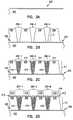
- FIGS. 2A through 2Killustrate a novel methodology for a selective electroless-plated copper metallization according to the teachings of the present invention.
- FIG. 2A through 2Killustrate a method for forming a multilayer copper (Cu) wiring structure on a substrate.
- the methodology of the present inventionavoids the need for a chemical mechanical planarization (CMP) process step in forming the same.
- a seed layer, or first seed layer, 202is deposited on a substrate 200 .
- depositing the first seed layer 202 on the substrate 200includes depositing a thin film of Palladium (Pd) on the substrate 200 .
- depositing the first seed layer 202 on the substrate 200includes depositing a thin film of Copper (Cu) on the substrate.
- the seed layer 202is deposited to have a thickness of less than 15 nanometers (nm).
- the seed layer 202is deposited to form a barely continuous film in the thickness range of 3 to 10 nm.
- the seed layer 202is deposited such that the seed layer possesses a discontinuous island structure in the thickness range of 3 to 10 nm.
- the seed layer 202is deposited using a physical vapor deposition process.
- the seed layer 202is deposited using a sputtering deposition technique.
- the seed layer 202is deposited using an evaporation deposition technique.
- FIG. 2Billustrates the structure following the next sequence of processing steps.
- a photolithography techniqueis used to define a number of via holes, or openings, 206 - 1 , 206 - 2 , . . . , 206 -N, above the seed layer 202 on the substrate 200 .
- using a photolithography technique to define a number of holes 206 - 1 , 206 - 2 , . . . , 206 -Nincludes patterning a photoresist layer 208 to define the number via holes, or openings, 206 - 1 , 206 - 2 , . . .
- a photoresist layercan be deposited over the seed layer 202 using any suitable technique, e.g. by spin coating. Then the photoresist can be masked, exposed, and washed to define the number of via holes, or openings, 206 - 1 , 206 - 2 , . . . , 206 -N to the seed layer 202 .
- the thickness of the photoresist layer 202is scalable.
- the deposition of the photoresist layer 208is controllable such that the photoresist thickness can be set at a predetermined height (h1).
- the scalable thickness of the photoresist layer 208determines a height (h1), or depth (h1) for the number of via holes, or openings, 206 - 1 , 206 - 2 , . . . , 206 -N.
- the structureis now as appears in FIG. 2B .
- FIG. 2Cillustrates the structure following the next sequence of processing steps.
- a layer of copper, first layer of copper, or first level of copper vias 210is deposited over the seed layer 202 using electroless plating.
- the layer of copper, first layer of copper, or first level of copper vias 210is formed in the number of via holes, or openings, 206 - 1 , 206 - 2 , . . . , 206 -N.
- Forming layer of copper, first layer of copper, or first level of copper vias 210includes filling the number of via holes, or openings, 206 - 1 , 206 - 2 , . . . , 206 -N to a top surface 214 of the first patterned photoresist layer 208 .
- depositing the layer of copper, first layer of copper, or first level of copper vias 210 over the seed layer 202is such that the layer of copper, first layer of copper, or first level of copper vias 210 form on the seed layer 202 but not on the patterned photoresist layer 208 .
- the structureis now as appears in FIG. 2C .
- FIG. 2Dillustrates the structure following the next sequence of processing steps.
- another seed layer, or second seed layer, 216is deposited on the first layer of copper, or first level of copper vias 210 and the top surface 214 of the first patterned photoresist layer 208 .
- depositing the second seed layer 216 on the first layer of copper, or first level of copper vias 210 and the top surface 214 of the first patterned photoresist layer 208includes depositing a thin film of Palladium (Pd).
- depositing the second seed layer 216 on the first layer of copper, or first level of copper vias 210 and the top surface 214 of the first patterned photoresist layer 208includes depositing a thin film of Copper (Cu).
- the second seed layer 216is deposited to have a thickness of less than 15 nanometers (nm). In one exemplary embodiment, the second seed layer 216 is deposited to form a barely continuous film in the thickness range of 3 to 10 nm. In another exemplary embodiment, the second seed layer 216 is deposited such that the second seed layer 216 possesses a discontinuous island structure 216 having an island thickness in the range of 3 to 10 nm.
- the second seed layer 216is deposited using a physical vapor deposition process.
- the second seed layer 216is deposited using a sputtering deposition technique.
- the second seed layer 216is deposited using an evaporation deposition technique.
- a second patterned photoresist layer 218is deposited above the second seed layer 216 , which defines a number of conductor line openings 220 - 1 , 220 - 2 , . . . , 220 -N. In one embodiment, depositing the second patterned photoresist layer 218 which defines a number of conductor line openings 220 - 1 , 220 - 2 , . . . , 220 -N, or first level metal line openings 220 - 1 , 220 - 2 , . . . , 220 -N. In one embodiment, the number of conductor line openings 220 - 1 , 220 - 2 , . . .
- 220 -Nare defined to form a number of conductor line openings 220 - 1 , 220 - 2 , . . . , 220 -N having a near minimum width and spacing. As one of ordinary skill in the art will understand upon reading this disclosure, this insures a sufficient space in the structure for a subsequent removal of the photoresist layers, e.g. first patterned photoresist layer 208 , on lower levels.
- a photoresist layercan be deposited over the second seed layer 216 using any suitable technique, e.g. by spin coating. Then the photoresist can be masked, exposed, and washed to define the number of conductor line openings 220 - 1 , 220 - 2 , . . . , 220 -N to the second seed layer 216 .
- the thickness of the second patterned photoresist layer 218is scalable. That is, the deposition of the photoresist layer 218 is controllable such that the photoresist thickness can be set at a predetermined height (h2).
- the scalable thickness of the second patterned photoresist layer 218determines a height (h2), or depth (h2) for the number of conductor line openings 220 - 1 , 220 - 2 , . . . , 220 -N.
- depositing the second patterned photoresist layer 218includes depositing the second patterned photoresist layer 218 to have a thickness (h2) which is less than a thickness (h1) of the first patterned photoresist layer 208 . That is, the thickness (h2) of the second patterned photoresist layer 218 , and consequently a depth (h2) of the number of conductor line openings 220 - 1 , 220 - 2 , . . . , 220 -N, is thinner than a depth (h1) of the first level of copper vias 210 defined by the thickness (h1) of the first patterned photoresist layer 208 .
- the structureis now as appears in FIG. 2D .
- FIG. 2Eillustrates the structure following the next sequence of processing steps.
- another layer of copper, second layer of copper, or first level of conductor lines 224is deposited or formed in the number of conductor line openings 220 - 1 , 220 - 2 , . . . , 220 -N using electroless plating.
- this next layer of copper, second layer of copper, or first level of conductor lines 224can be deposited in the number of conductor line openings 220 - 1 , 220 - 2 , . . . , 220 -N using electroless plating.
- forming this next layer of copper, second layer of copper, or first level of conductor lines 224includes filling the number of conductor line openings 220 - 1 , 220 - 2 , . . . , 220 -N to a top surface 226 of the second patterned photoresist layer 218 .
- depositing this next layer of copper, second layer of copper, or first level of conductor lines 224 over the second seed layer 216is such that this next layer of copper, second layer of copper, or first level of conductor lines 224 form on the second seed layer 216 but not on the second patterned photoresist layer 218 .
- the structureis now as appears in FIG. 2E .
- FIG. 2Fillustrates the structure after the following sequence of processing steps.
- the first patterned photoresist layer 208 and the second patterned photoresist layer 218are removed.
- removing the first patterned photoresist layer 208 and the second patterned photoresist layer 218includes removing the first patterned photoresist layer 208 and the second patterned photoresist layer 218 using an oxygen plasma etching.
- the methodfurther includes removing the first and second seed layers 202 and 216 with the photoresist layers 208 and 218 from areas on the substrate 200 which are not beneath the number of copper vias 210 or between the conductive metal lines 224 and the vias 210 .
- thisis due the present inventions novel methodology where the seed layers, 202 and 216 , are deposited to have a thickness of less than 15 nanometers (nm), thus forming a barely continuous thin film and/or discontinuous island structure.
- Other suitable techniques for removing the first patterned photoresist layer 208 and the second patterned photoresist layer 218can similarly be employed.
- a thin diffusion barrier 228can be formed on the exposed first level of copper vias 210 and first level of conductor lines 224 as well as the remaining, exposed first and second seed layers, 202 and 216 respectively, located between the substrate, vias, and metal lines.
- forming a thin diffusion barrier 228includes forming a thin diffusion barrier of Tungsten Silicon Nitride (WSi x N y ) 228 having a thickness of less than 8 nanometers (nm).
- forming a thin diffusion barrier of Tungsten Silicon Nitride (WSi x N y ) 228 having a thickness of less than 8 nanometers (nm)includes forming a graded composition of WSi x , where x varies from 2.0 to 2.5, and nitriding the graded composition of WSi x .
- the details of forming a thin diffusion barrier 228are further described in detail in a co-filed, co-pending application; attorney docket # 303.648US1, entitled, “Method for Making Copper Interconnects in Integrated Circuits,” which is hereby incorporated by reference. The structure is now as appears in FIG. 2F .
- the removal of the first patterned photoresist layer 208 and the second patterned photoresist layer 218can be delayed until these subsequent layer are completed, the invention is not so limited. That is, if subsequent layers are to be fabricated, the steps illustrated in FIG. 2F will be delayed and the process will repeat the sequence provided in FIG. 2A-2E .
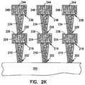
- FIG. 2Gillustrates the forming of subsequent via and metallization layers prior to the process steps of FIG. 2F and continuing in sequence after the number of process steps completed in FIG. 2E .
- FIG. 2Gshows that in forming subsequent conductive via and metallization layers, another seed layer, or third seed layer, 229 is deposited on the second layer of copper, or first level of conductor lines 224 and the top surface 226 of the second patterned photoresist layer 218 .
- depositing the third seed layer 229 on the second layer of copper, or first level of conductor lines 224 and the top surface 226 of the second patterned photoresist layer 218includes depositing a thin film of Palladium (Pd).
- depositing the third seed layer 229 on the second layer of copper, or first level of conductor lines 224 and the top surface 226 of the second patterned photoresist layer 218includes depositing a thin film of Copper (Cu).
- the third seed layer 229is deposited to have a thickness of less than 15 nanometers (nm).
- the third seed layer 229is deposited to form a barely continuous film in the thickness range of 3 to 10 nm.
- the third seed layer 229is deposited such that the third seed layer 229 possesses a discontinuous island structure 229 having an island thickness in the range of 3 to 10 nm.
- the third seed layer 229is deposited using a physical vapor deposition process.
- the third seed layer 229is deposited using a sputtering deposition technique.
- the third seed layer 229is deposited using an evaporation deposition technique.
- a third patterned photoresist layer 230is deposited above the third seed layer 229 , which defines a number of via holes, or openings, 232 - 1 , 232 - 2 , . . . , 232 -N to the third seed layer 229 .
- a photoresist layercan be deposited over the third seed layer 229 using any suitable technique, e.g. by spin coating.
- the photoresistcan be masked, exposed, and washed to define the number of via holes, or openings, 232 - 1 , 232 - 2 , . . . , 232 -N to the third seed layer 229 .
- the thickness of the second patterned photoresist layer 218is scalable. That is, the deposition of the photoresist layer 230 is controllable such that the photoresist thickness can be set at a predetermined height (h3).
- the scalable thickness of the second patterned photoresist layer 230determines a height (h3) for the number of via holes, or openings, 232 - 1 , 232 - 2 , . . . , 232 -N.
- the structureis now as appears in FIG. 2G .
- FIG. 2Hillustrates the structure continuing on from the process steps included in FIG. 2G .
- another layer of copper, third layer of copper, or second level of copper vias 234is deposited or formed over the third seed layer 229 using electroless plating.
- the third layer of copper, or second level of copper vias 234is formed in the number of via holes, or openings, 232 - 1 , 232 - 2 , . . . , 232 -N to the third seed layer 229 .
- Forming the third layer of copper, or second level of copper vias 234includes filling the number of via holes, or openings, 232 - 1 , 232 - 2 , . . . , 232 -N to a top surface 236 of the third patterned photoresist layer 230 .
- depositing third layer of copper, or second level of copper vias 234 over the third seed layer 229is such that the third layer of copper, or second level of copper vias 234 form on the third seed layer 229 but not on the third patterned photoresist layer 230 .
- the structureis now as appears in FIG. 2H .
- FIG. 2Iillustrates the structure following the next sequence of processing steps.
- another seed layer, or fourth seed layer, 238is deposited on the third layer of copper, or second level of copper vias 234 and the top surface 236 of the third patterned photoresist layer 230 .
- depositing the fourth seed layer 238 on the third layer of copper, or second level of copper vias 234 and the top surface 236 of the third patterned photoresist layer 230includes depositing a thin film of Palladium (Pd).
- depositing the fourth seed layer 238 on the third layer of copper, or second level of copper vias 234 and the top surface 236 of the third patterned photoresist layer 230includes depositing a thin film of Copper (Cu).
- the fourth seed layer 238is deposited to have a thickness of less than 10 nanometers (nm). In one exemplary embodiment, the fourth seed layer 238 is deposited to form a barely continuous film in the thickness range of 3 to 10 nm. In another exemplary embodiment, the fourth seed layer 238 is deposited such that the fourth seed layer 238 possesses a discontinuous island structure 238 having an island thickness in the range of 3 to 10 nm.
- the fourth seed layer 238is deposited using a physical vapor deposition process.
- the fourth seed layer 238is deposited using a sputtering deposition technique.
- the fourth seed layer 238is deposited using an evaporation deposition technique.
- a fourth patterned photoresist layer 240is deposited above the fourth seed layer 238 , which defines a number of conductor line openings 242 - 1 , 242 - 2 , . . . , 242 -N.
- depositing the fourth patterned photoresist layer 240 which defines a number of conductor line openings 242 - 1 , 242 - 2 , . . . , 242 -Nincludes defining a number of second level metal line openings 242 - 1 , 242 - 2 , . . . , 242 -N.
- 242 -Nare defined to form a number of conductor line openings 242 - 1 , 242 - 2 , . . . , 242 -N having a near minimum width and spacing. As one of ordinary skill in the art will understand upon reading this disclosure, this insures a sufficient space in the structure for a subsequent removal of the photoresist layers, e.g. first, second, and third patterned photoresist layer 208 , 218 , and 230 on lower levels.
- the photoresist layerse.g. first, second, and third patterned photoresist layer 208 , 218 , and 230 on lower levels.
- a photoresist layercan be deposited over the fourth seed layer 238 using any suitable technique, e.g. by spin coating. Then the photoresist can be masked, exposed, and washed to define the number of conductor line openings 242 - 1 , 242 - 2 , . . . , 242 -N to the fourth seed layer 238 .
- the thickness of the fourth patterned photoresist layer 240is scalable. That is, the deposition of the fourth patterned photoresist layer 240 is controllable such that the photoresist thickness can be set at a predetermined height (h4).
- the scalable thickness of the fourth patterned photoresist layer 240determines a height (h4) for the number of conductor line openings 242 - 1 , 242 - 2 , . . . , 242 -N.
- depositing the fourth patterned photoresist layer 240includes depositing the fourth patterned photoresist layer 240 to have a thickness (h4) which is less than a thickness (h3) of the third patterned photoresist layer 230 . That is, the thickness (h3) of the third patterned photoresist layer 230 is thinner than a depth (h3) of the second level of copper vias 234 defined by the thickness (h3) of the third patterned photoresist layer 230 .
- the structureis now as appears in FIG. 21 .
- FIG. 2Jillustrates the structure following the next sequence of processing steps.
- another layer of copper, fourth layer of copper, or second level of conductor lines 244is deposited or formed in the number of conductor line openings 242 - 1 , 242 - 2 , . . . , 242 -N using electroless plating.
- this fourth layer of copper, or second level of conductor lines 244can be deposited in the number of conductor line openings 242 - 1 , 242 - 2 , . . . , 242 -N using electroless plating.
- this fourth layer of copper, or second level of conductor lines 244includes filling the number of conductor line openings 242 - 1 , 242 - 2 , . . . , 242 -N to a top surface 246 of the fourth patterned photoresist layer 240 .
- depositing this fourth layer of copper, or second level of conductor lines 244 over the fourth seed layer 238is such that this fourth layer of copper, or second level of conductor lines 244 form on the fourth seed layer 238 but not on the fourth patterned photoresist layer 240 .
- the structureis now as appears in FIG. 2J .
- FIG. 2Killustrates the structure after the following sequence of processing steps.
- the first, second, third, and fourth patterned photoresist layers 208 , 218 , 230 , and 240are removed.
- removing the first, second, third, and fourth patterned photoresist layers 208 , 218 , 230 , and 240includes removing the first, second, third, and fourth patterned photoresist layers 208 , 218 , 230 , and 240 using an oxygen plasma etching.
- the methodfurther includes removing the first, second, third, and fourth seed layers, 202 , 216 , 229 and 238 respectively, with the photoresist layers from areas on the substrate which are not beneath the number of copper vias or between the conductive metal lines and the vias.
- thisis due the present inventions novel methodology where the seed layers, 202 , 216 , 229 and 238 , are deposited to have a thickness of less than 15 nanometers (nm), thus forming a barely continuous thin film and/or discontinuous island structure.
- first, second, third, and fourth patterned photoresist layers 208 , 218 , 230 , and 240can similarly be employed.
- the first, second, third, and fourth patterned photoresist layers 208 , 218 , 230 , and 240can be removed at earlier or later stages of a fabrication process, as described herein, depending on the number of via and metal levels to be formed.
- a thin diffusion barrier 248can be formed on the exposed first and second level of copper vias 210 , 234 and the exposed first and second level of conductor lines 224 , 244 as well as the remaining, exposed first, second, third, and fourth seed layers, 202 , 216 , 229 and 238 respectively, located between the substrate, vias, and metal lines.
- forming a thin diffusion barrier 248includes forming a thin diffusion barrier of Tungsten Silicon Nitride (WSi x N y ) 248 having a thickness of less than 8 nanometers (nm).
- forming a thin diffusion barrier of Tungsten Silicon Nitride (WSi x N y ) 248 having a thickness of less than 8 nanometers (nm)includes forming a graded composition of WSi x , where x varies from 2.0 to 2.5, and nitriding the graded composition of WSi x .
- the details of forming a thin diffusion barrier 228are further described in detail in a co-filed, co-pending application; attorney docket # 303.648us1, entitled, “Method for Making Copper Interconnects in Integrated Circuits,” which is hereby incorporated by reference. The structure is now as appears in FIG. 2K .
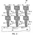
- FIG. 3is an illustration of an integrated circuit 300 formed according to the teachings of the present invention.
- the integrated circuit 300includes a multilayer copper wiring structure.
- the integrated circuit 300includes at least one semiconductor device 301 formed in a substrate 302 .
- a first number of seed layers 304 - 1 , 304 - 2 , . . . , 304 -Nare formed on a number of portions 305 - 1 , 305 - 2 , . . . , 305 -N of the at least one semiconductor device.
- the at least one semiconductor device 301includes the number of portions 305 - 1 , 305 - 2 , . . . , 305 -N of a semiconductor device 301 which require electrical contact to subsequent integrated circuit layers formed above the semiconductor device 301 .
- the at least one semiconductor device 301can include at least one transistor 301 which has a source and a drain region.
- the number of portions 305 - 1 , 305 - 2 , . . . , 305 -N of a semiconductor device 301 which require electrical contact to subsequent integrated circuit layers formed above the semiconductor device 301include the source and the drain regions 305 - 1 , 305 - 2 , . . . , 305 -N.
- a number of copper vias 307 - 1 , 307 - 2 , . . . , 307 -N, or first level of copper vias 307 - 1 , 307 - 2 , . . . , 307 -N,are formed above and contact with the first number of seed layers 304 - 1 , 304 - 2 , . . . , 304 -N.
- the first number of seed layers 304 - 1 , 304 - 2 , . . . , 304 -Ninclude a thin film of Palladium (Pd) or Copper.
- the first number of seed layers 304 - 1 , 304 - 2 , . . . , 304 -Nhave a thickness of less than 15 nanometers (nm).
- the first number of seed layers 304 - 1 , 304 - 2 , . . . , 304 -Nincludes a first number of seed layers 304 - 1 , 304 - 2 , . . . , 304 -N having a discontinuous island structure with an island thickness in the range of 3 to 10 nanometers.
- a second number of seed layers 309 - 1 , 309 - 2 , . . . , 309 -Nare formed on the number of copper vias 307 - 1 , 307 - 2 , . . . , 307 -N.
- the second number of seed layers 309 - 1 , 309 - 2 , . . . , 309 -Ninclude a thin film of Palladium (Pd) or Copper.
- the second number of seed layers 309 - 1 , 309 - 2 , . . . , 309 -Nhave a thickness of less than 15 nanometers (nm).
- the second number of seed layers 309 - 1 , 309 - 2 , . . . , 309 -Nincludes a second number of seed layers 309 - 1 , 309 - 2 , . . . , 309 -N having a discontinuous island structure with an island thickness in the range of 3 to 10 nanometers.
- a number of conductor metal lines 311 - 1 , 311 - 2 , . . . , 311 -N, or first level of conductor metal lines 311 - 1 , 311 - 2 , . . . , 311 -N,are formed above and contact with the second number of seed layers 309 - 1 , 309 - 2 , . . . , 309 -N.
- the first level of conductor metal lines 311 - 1 , 311 - 2 , . . . , 311 -Nincludes a number of copper metal lines 311 - 1 , 311 - 2 , . . . , 311 -N.
- the integrated circuit 300further includes a thin diffusion barrier 315 covering the number of copper vias 307 - 1 , 307 - 2 , . . . , 307 -N, the number of conductor metal lines 311 - 1 , 311 - 2 , . . . , 311 -N, and the first and the second number of seed layers, 304 - 1 , 304 - 2 , . . . , 304 -N, and 309 - 1 , 309 - 2 , . . . , 309 -N respectively.
- the thin diffusion barrier 315has a thickness of less than 8.0 nanometers (nm). In one embodiment, the thin diffusion barrier has a thickness in the range of 2.0 to 6.0 nanometers. In one embodiment, the thin diffusion barrier 315 includes a graded composition of Tungsten Silicon Nitride (WSi x N y ), and wherein x varies from 2.0 to 2.5.
- WSi x N yTungsten Silicon Nitride
- the integrated circuit, or multilayer copper wiring structure 300includes a third number of seed layers 317 - 1 , 317 - 2 , . . . , 317 -N, including a thin film of Palladium (Pd) or Copper, are formed on the first level of copper metal lines 311 - 1 , 311 - 2 , . . . , 311 -N, or first level of conductor metal lines 311 - 1 , 311 - 2 , . . . , 311 -N. Further, the third number of seed layers 317 - 1 , 317 - 2 , . . .
- the third number of seed layers 317 - 1 , 317 - 2 , . . . , 317 -Nincludes a third number of seed layers 317 - 1 , 317 - 2 , . . . , 317 -N having a discontinuous island structure with an island thickness in the range of 3 to 10 nanometers.
- a second level of copper vias 319 - 1 , 319 - 2 , . . . , 319 -Nare formed above and contacting the third number of seed layers 317 - 1 , 317 - 2 , . . . , 317 -N.
- the fourth number of seed layers 321 - 1 , 321 - 2 , . . . , 321 -Nincludes a fourth number of seed layers 321 - 1 , 321 - 2 , . . . , 321 -N having a discontinuous island structure with an island thickness in the range of 3 to 10 nanometers.
- a second level of copper metal lines 323 - 1 , 323 - 2 , . . . , 323 -N, or second level of conductor metal lines 323 - 1 , 323 - 2 , . . . , 323 -N,are formed above and contacting fourth number of seed layers 321 - 1 , 321 - 2 , . . . , 321 -N.
- the thin diffusion barrier 315further covers the second level of copper vias 319 - 1 , 319 - 2 , . . . , 319 -N, the second level of copper metal lines 323 - 1 , 323 - 2 , . . . , 323 -N, and the third, and fourth number of seed layers, 317 - 1 , 317 - 2 , . . . , 317 -N and 321 - 1 , 321 - 2 , . . . , 321 -N respectively.
- the present inventionprovides for a multilayer copper wiring structure by electroless, selectively deposited copper which will not require chemical mechanical planarization (CMP).
- CMPchemical mechanical planarization
- the present inventionis streamlined and significantly reduces the amount of deposited conductive material, e.g. copper, which is ultimately discarded according to conventional processes. This also alleviates important environmental concerns regarding the disposition of used materials. Further, by avoiding the need for a CMP process step the usage of consumables such as pads and slurry is conserved.
Landscapes
- Engineering & Computer Science (AREA)
- Physics & Mathematics (AREA)
- Condensed Matter Physics & Semiconductors (AREA)
- General Physics & Mathematics (AREA)
- Computer Hardware Design (AREA)
- Microelectronics & Electronic Packaging (AREA)
- Power Engineering (AREA)
- Manufacturing & Machinery (AREA)
- Internal Circuitry In Semiconductor Integrated Circuit Devices (AREA)
Abstract
Description
- This application is a Divisional of U.S. application Ser. No. 09/483,881, filed Jan. 18, 2000, which is incorporated herein by reference.
- This application is related to the following co-filed and commonly assigned applications; U.S. application Ser. No. 09/488,098, filed Jan. 18, 2000, now U.S. Pat. No. 6,429,120 and U.S. application Ser. No. 09/484,303, filed Jan. 18, 2000, both of which are hereby incorporated by reference.
- The present invention relates generally to integrated circuits. More particularly, it pertains to structures and methods for selective electroless-plated copper metallization.
- The rapid progress in miniaturization of integrated circuits (IC) is leading to denser and finer pitched chips with ever increasing performance. In order to enhance the performance of advanced ICs, the interconnect systems are gradually migrating from aluminum-based metallurgy to higher-conductivity and more electromigration-resistant copper. Of the several schemes proposed for fabricating copper interconnects, the most promising method appears to be the Damascene process. Using this method, the trenches and vias are patterned in blanket dielectrics, and then metal is deposited into the trenches and holes in one step, followed by chemical mechanical polishing (CMP) to remove the unwanted surface metal. This leaves the desired metal in the trenches and holes, and a planarized surface for subsequent metallization. During the CMP process, especially for the via holes, more than 99% of the deposited copper is removed, and this is a very wasteful and expensive process, which includes a high usage of consumables such as pads and slurry. Furthermore, the disposition of used materials is a very important environmental issue. Therefore it is highly desirable to accomplish the copper metallization without CMP.
- One approach to the formation of copper vias and metal lines includes the electroless deposition of copper. Electroless deposition of copper is used in printed circuit boards to manufacture copper lines and through holes where the line and hole dimensions are in the several tens to hundreds of microns. The is, of course, much larger than the sub-micron design rules for integrated circuit fabrication on silicon wafers. In this approach, Palladium (Pd) is often used as the activated base metal for electroless copper plating. Several different groups have shown the success of the same. For example, an article published by Bhansali and D. K. Sood, entitled, “A novel technique for fabrication of metallic structure on polyimide by selective electroless copper plating using ion implantation,” Thin Solid Films, vol. 270, p. 489-492, 1995, successfully used palladium ion implantation into polyimide to seed an electroless plated copper film on the polyimide surface. An ion dose range of 1.5×10¹⁵to 1.2×10¹⁷ions/cm2was used. They also reported on the successful use of copper implantation into silicon to seed the electroless plating using a dose range of 5×10¹⁴to 6.4×10¹⁶ions/cm2. (See, Bhansali, S. et al, “Selective electroless copper plating on silicon seeded by copper ion implantation”, Thin Solid Films, vol. 253, no. 1-2, p. 391-394, 1994). An article published by M.-H. Kiang, et al, entitled, “Pd/Si plasma immersion ion implantation for selective electroless copper plating on SiO2, Applied Physics Letters, vol. 60, no. 22, p. 2767-2769, 1992, demonstrated selective deposition of copper in SiO2trenches using Pd/Si plasma immersion ion implantation and electroless copper plating. An article published by J.-Y. Zhang et al, entitled, “Investigations of photo-induced decomposition of palladium acetate for electroless copper plating”, Thin Solid Films, vol. 318, p. 234-238, 1998, illustrates photo-induced palladium decomposition of acetate performed by using argon and xenon excimer vacuum ultraviolet sources in the formation of palladium, which acted as a catalyst for subsequent copper plating by means of an electroless bath for selective copper deposition. An article published by M.-H. Bernier et al, entitled, “Laser processing of palladium for selective electroless copper plating”, SPIE Proc., vol. 2045, p. 330-337, 1993 demonstrated that the direct writing of palladium features by the Ar+ laser-induced pyrolytic decomposition of an organometallic palladium resins on polyimide and Si3N4led to active Pd sites which were selectively copper plated. Also, as described in an article published by J.-L. Yeh et al, entitled, “Selective Copper Plating of Polysilicon surface Micromachined Structures”, Technical digest of 1998 Solid-State Sensor and Actuator Workshop, Transducer Research Foundation Catalog No. 98TRF-0001, p.248-251, 1998, Yeh et al. exposed polycrystalline silicon structures to a palladium solution that selectively activated the polysilicon structure, but not the silicon oxide or nitride layers. Upon immersion into a copper plating solution at a temperature between 55 and 80° C., the copper nuclei were initially formed on the Pd+ activated polysilicon surface. After the formation of a thin-layer copper, copper started to deposit on this thin initiated copper film. Recently, an article published by V. M. Dubin et al, entitled, “Selective and Blanket Electroless Copper Deposition for Ultralarge Scale Integration”, J. Electrochem. Soc., vol. 144, no. 3, p. 898-908, 1997, disclosed a novel seeding method for electroless copper deposition on sputtered copper films with an aluminum protection layer. This seeding method consisted of (I) deposition of Cu seed layer by sputtering or evaporation, (ii) deposition of a sacrificial thin aluminum layer without breaking vacuum, (iii) etching the aluminum layer in the electroless Cu plating bath, followed by electroless Cu deposition.
- Here, Dubin et al. designed and constructed a single-wafer electroless copper deposition tool with up to 200 mm wafer capability, and an electroless copper deposition process was developed. Electroless Cu films deposited at high plating rate (up to 120 nm/min) in solutions with optimized plating chemical environment exhibited low resistivity (<2 μohm cm for as deposited films), low surface roughness, and good electrical uniformity.
- All of these above described methods are rather complex which means that the number of process steps involved in integrated circuit fabrication increases. The problem associated with these methods is that an increase in the number of process steps makes integrated circuit fabrication more costly. Further, none of the above described methods address or provide a resolution to the costly excess expenditure of materials and the environmental concerns when such processes are implemented to form sub-micron vias and metal lines on wafers in a conventional CMP fabrication process.
- For the reasons stated above and for others which will become apparent from reading the following disclosure, structures and methods are needed which alleviate the problems associated with via and metal line fabrication processes. These structures and methods for via and metal line fabrication must be streamlined and accommodate the demand for higher performance in integrated circuits even as the fabrication design rules shrink.
- The above mentioned problems associated with integrated circuit size and performance, the via and metal line formation process, and other problems are addressed by the present invention and will be understood by reading and studying the following specification. Structures and methods are provided which include a selective electroless copper metallization. The present invention provides for a multilayer copper wiring structure by electroless, selectively deposited copper in a streamlined process which will not require chemical mechanical planarization (CMP). Thus, the present invention significantly reduces the amount of deposited conductive material, e.g. copper, which is ultimately discarded according to conventional processes. This alleviates important environmental concerns regarding the disposition of used materials. Further, by avoiding the need for a CMP process step, the usage of consumables such as pads and slurry is conserved.
- In particular, an illustrative embodiment of the present invention includes a novel methodology for forming copper vias on a substrate. This method includes depositing a thin film seed layer of Palladium (Pd) or Copper (Cu) on a substrate. The seed layer is deposited to a thickness of less than 15 nanometers (nm). A photolithography technique is used to define a number of via holes above the seed layer. In one embodiment, using a photolithography technique includes forming a patterned photoresist layer to define the number of via holes above the seed layer. A layer of copper is deposited over the seed layer using electroless plating filling the number of via holes to a top surface of the patterned photoresist layer. The method can be repeated any number of times depositing a second seed layer, depositing another patterned photoresist layer defining a number of conductor line openings above the second seed layer, and forming a second layer of copper using electroless plating which fills the number of conductor line openings to a top surface of the second patterned photoresist layer. The photoresist layers along with the seed layers in other regions can then be removed by ashing and a chemical mechanical planarization process is avoided. Structures formed by this novel process are similarly included within the scope of the present invention.
- These and other embodiments, aspects, advantages, and features of the present invention will be set forth in part in the description which follows, and in part will become apparent to those skilled in the art by reference to the following description of the invention and referenced drawings or by practice of the invention. The aspects, advantages, and features of the invention are realized and attained by means of the instrumentalities, procedures, and combinations particularly pointed out in the appended claims.
- The following detailed description of the preferred embodiments can best be understood when read in conjunction with the following drawings, in which:
FIGS. 1A-1B illustrate an embodiment of the various processing steps for forming vias and metal lines according to the teachings of the prior art;FIGS. 2A-2K illustrate an embodiment of the various processing steps for a selective electroless-plated copper metallization according to the teachings of the present invention.FIG. 3 is an illustration of an integrated circuit formed according to the teachings of the present invention.- In the following detailed description of the invention, reference is made to the accompanying drawings which form a part hereof, and in which is shown, by way of illustration, specific embodiments in which the invention may be practiced. These embodiments are described in sufficient detail to enable those skilled in the art to practice the invention. Other embodiments may be utilized and structural, logical, and electrical changes may be made without departing from the scope of the present invention.
- The terms wafer and substrate used in the following description include any structure having an exposed surface with which to form the integrated circuit (IC) structure of the invention. The term substrate is understood to include semiconductor wafers. The term substrate is also used to refer to semiconductor structures during processing, and may include other layers that have been fabricated thereupon. Substrate include doped and undoped semiconductors, epitaxial semiconductor layers supported by a base semiconductor or insulator, as well as other semiconductor structures well known to one skilled in the art. The term insulator is defined to include any material that is less electrically conductive than the materials generally referred to as conductors by those skilled in the art. The following detailed description is, therefore, not to be taken in a limiting sense.
FIGS. 1A-1B illustrate an embodiment of the various processing steps for forming vias and metal lines according to the teachings of the prior art. As shown inFIG. 1A , a number of vias101-1 and101-2 are formed in aninsulator material 103, e.g. silicon dioxide (SiO2), contacting with asubstrate 100. As one of ordinary skill in the art will recognize, any number of semiconductor devices can be formed in the substrate to which the number of vias101-1 and101-2 make electrical contact.- Conventionally, to form vias and aluminum wire metal lines, fabricators use a dual-damascene metallization technique, which takes its name from the ancient Damascene metalworking art of inlaying metal in grooves or channels to form ornamental patterns. The dual-damascene technique entails covering the components on a wafer with an
insulative layer 103, etching small holes in theinsulative layer 103 to expose portions of the components underneath insubstrate 100, and subsequently etching shallow trenches from hole to hole to define a number of metal lines. Fabricators then blanket the entire insulative layer with a layer of aluminum or other conductive material and polish off the excess, leaving behind conductive vias, or contact plugs, in the holes and conductive lines in the trenches. - As shown in the prior art of
FIG. 1A , a layer ofcopper 104 can be deposited in the holes and trenches using an electroplated copper deposition technique. As shown inFIG. 1A , thecopper layer 104 fills the holes and the trenches, but also covers all of the surfaces features such theinsulator material 103 used in the dual damascene process. FIG. 1B illustrates the structure after the excess copper has been removed through a chemically mechanical planarization (CMP) process step. As shown in the prior artFIG. 1B , the CMP process step polishes the deposited layer ofcopper 104 down to and level with the top surface of theinsulator layer 103 to form the copper vias101-1 and101-2 as well as copper metal lines105-1 and105-2. One of ordinary skill in the art will understand, upon viewing the fabrication process illustrated inFIGS. 1A and 1B , the wastefulness in the amount of copper which is discarded in the CMP process step.- Method of the Present Invention
FIGS. 2A through 2K illustrate a novel methodology for a selective electroless-plated copper metallization according to the teachings of the present invention. Specifically,FIG. 2A through 2K illustrate a method for forming a multilayer copper (Cu) wiring structure on a substrate. The methodology of the present invention avoids the need for a chemical mechanical planarization (CMP) process step in forming the same. As shown inFIG. 2A , a seed layer, or first seed layer,202 is deposited on asubstrate 200. In one embodiment, depositing thefirst seed layer 202 on thesubstrate 200 includes depositing a thin film of Palladium (Pd) on thesubstrate 200. In another embodiment, depositing thefirst seed layer 202 on thesubstrate 200 includes depositing a thin film of Copper (Cu) on the substrate. Theseed layer 202 is deposited to have a thickness of less than 15 nanometers (nm). In one exemplary embodiment, theseed layer 202 is deposited to form a barely continuous film in the thickness range of 3 to 10 nm. In another exemplary embodiment, theseed layer 202 is deposited such that the seed layer possesses a discontinuous island structure in the thickness range of 3 to 10 nm. In one embodiment, theseed layer 202 is deposited using a physical vapor deposition process. For example, in one embodiment, theseed layer 202 is deposited using a sputtering deposition technique. In another embodiment, theseed layer 202 is deposited using an evaporation deposition technique. One of ordinary skill in the art will understand, upon reading this disclosure, the manner in which such physical vapor deposition processes can be performed to form theseed layer 202 described herein.FIG. 2B illustrates the structure following the next sequence of processing steps. InFIG. 2B , a photolithography technique is used to define a number of via holes, or openings,206-1,206-2, . . . ,206-N, above theseed layer 202 on thesubstrate 200. As one of ordinary skill in the art will understand upon reading this disclosure, using a photolithography technique to define a number of holes206-1,206-2, . . . ,206-N, includes patterning aphotoresist layer 208 to define the number via holes, or openings,206-1,206-2, . . . ,206-N over theseed layer 202. One of ordinary skill in the art will also understand upon reading this disclosure, the manner of forming the patterned photoresist layer, or first patterned photoresist layer,208. For example, a photoresist layer can be deposited over theseed layer 202 using any suitable technique, e.g. by spin coating. Then the photoresist can be masked, exposed, and washed to define the number of via holes, or openings,206-1,206-2, . . . ,206-N to theseed layer 202. One of ordinary skill in the art will further understand, upon reading this disclosure, that the thickness of thephotoresist layer 202 is scalable. That is, the deposition of thephotoresist layer 208 is controllable such that the photoresist thickness can be set at a predetermined height (h1). Thus, the scalable thickness of thephotoresist layer 208 determines a height (h1), or depth (h1) for the number of via holes, or openings,206-1,206-2, . . . ,206-N. The structure is now as appears inFIG. 2B .FIG. 2C illustrates the structure following the next sequence of processing steps. InFIG. 2C , a layer of copper, first layer of copper, or first level ofcopper vias 210 is deposited over theseed layer 202 using electroless plating. One of ordinary skill in the art will understand upon reading this disclosure the various manner in which the layer of copper, first layer of copper, or first level ofcopper vias 210 can be deposited over theseed layer 202 using electroless plating. According to the teachings of the present invention, the layer of copper, first layer of copper, or first level ofcopper vias 210 is formed in the number of via holes, or openings,206-1,206-2, . . . ,206-N. Forming layer of copper, first layer of copper, or first level ofcopper vias 210 includes filling the number of via holes, or openings,206-1,206-2, . . . ,206-N to atop surface 214 of the firstpatterned photoresist layer 208. According to the teachings of the present invention depositing the layer of copper, first layer of copper, or first level ofcopper vias 210 over theseed layer 202 is such that the layer of copper, first layer of copper, or first level ofcopper vias 210 form on theseed layer 202 but not on the patternedphotoresist layer 208. The structure is now as appears inFIG. 2C .FIG. 2D illustrates the structure following the next sequence of processing steps. InFIG. 2D , another seed layer, or second seed layer,216 is deposited on the first layer of copper, or first level ofcopper vias 210 and thetop surface 214 of the firstpatterned photoresist layer 208. In one embodiment, depositing thesecond seed layer 216 on the first layer of copper, or first level ofcopper vias 210 and thetop surface 214 of the firstpatterned photoresist layer 208 includes depositing a thin film of Palladium (Pd). In another embodiment, depositing thesecond seed layer 216 on the first layer of copper, or first level ofcopper vias 210 and thetop surface 214 of the firstpatterned photoresist layer 208 includes depositing a thin film of Copper (Cu). As before, thesecond seed layer 216 is deposited to have a thickness of less than 15 nanometers (nm). In one exemplary embodiment, thesecond seed layer 216 is deposited to form a barely continuous film in the thickness range of 3 to 10 nm. In another exemplary embodiment, thesecond seed layer 216 is deposited such that thesecond seed layer 216 possesses adiscontinuous island structure 216 having an island thickness in the range of 3 to 10 nm.- In one embodiment, the
second seed layer 216 is deposited using a physical vapor deposition process. For example, in one embodiment, thesecond seed layer 216 is deposited using a sputtering deposition technique. In another embodiment, thesecond seed layer 216 is deposited using an evaporation deposition technique. One of ordinary skill in the art will understand, upon reading this disclosure, the manner in which such physical vapor deposition processes can be performed to form thesecond seed layer 216 described herein. - A second
patterned photoresist layer 218 is deposited above thesecond seed layer 216, which defines a number of conductor line openings220-1,220-2, . . . ,220-N. In one embodiment, depositing the secondpatterned photoresist layer 218 which defines a number of conductor line openings220-1,220-2, . . . ,220-N, or first level metal line openings220-1,220-2, . . . ,220-N. In one embodiment, the number of conductor line openings220-1,220-2, . . . ,220-N are defined to form a number of conductor line openings220-1,220-2, . . . ,220-N having a near minimum width and spacing. As one of ordinary skill in the art will understand upon reading this disclosure, this insures a sufficient space in the structure for a subsequent removal of the photoresist layers, e.g. first patternedphotoresist layer 208, on lower levels. This consideration is described in greater detail in a co-pending, co-filed application, client docket # 99-0673 entitled, “A Multilevel Copper Interconnect with Double Insulation for ULSI.” One of ordinary skill in the art will understand upon reading this disclosure, the manner of forming the secondpatterned photoresist layer 218. For example, a photoresist layer can be deposited over thesecond seed layer 216 using any suitable technique, e.g. by spin coating. Then the photoresist can be masked, exposed, and washed to define the number of conductor line openings220-1,220-2, . . . ,220-N to thesecond seed layer 216. One of ordinary skill in the art will further understand, upon reading this disclosure, that the thickness of the secondpatterned photoresist layer 218 is scalable. That is, the deposition of thephotoresist layer 218 is controllable such that the photoresist thickness can be set at a predetermined height (h2). Thus, the scalable thickness of the secondpatterned photoresist layer 218 determines a height (h2), or depth (h2) for the number of conductor line openings220-1,220-2, . . . ,220-N. According to the teachings of the present invention, depositing the secondpatterned photoresist layer 218 includes depositing the secondpatterned photoresist layer 218 to have a thickness (h2) which is less than a thickness (h1) of the firstpatterned photoresist layer 208. That is, the thickness (h2) of the secondpatterned photoresist layer 218, and consequently a depth (h2) of the number of conductor line openings220-1,220-2, . . . ,220-N, is thinner than a depth (h1) of the first level ofcopper vias 210 defined by the thickness (h1) of the firstpatterned photoresist layer 208. The structure is now as appears inFIG. 2D . FIG. 2E illustrates the structure following the next sequence of processing steps. InFIG. 2E , another layer of copper, second layer of copper, or first level ofconductor lines 224 is deposited or formed in the number of conductor line openings220-1,220-2, . . . ,220-N using electroless plating. One of ordinary skill in the art will understand upon reading this disclosure the various manner in which this next layer of copper, second layer of copper, or first level ofconductor lines 224 can be deposited in the number of conductor line openings220-1,220-2, . . . ,220-N using electroless plating. According to the teachings of the present invention, forming this next layer of copper, second layer of copper, or first level ofconductor lines 224 includes filling the number of conductor line openings220-1,220-2, . . . ,220-N to atop surface 226 of the secondpatterned photoresist layer 218. According to the teachings of the present invention depositing this next layer of copper, second layer of copper, or first level ofconductor lines 224 over thesecond seed layer 216 is such that this next layer of copper, second layer of copper, or first level ofconductor lines 224 form on thesecond seed layer 216 but not on the secondpatterned photoresist layer 218. The structure is now as appears inFIG. 2E .FIG. 2F illustrates the structure after the following sequence of processing steps. InFIG. 2F , according to the teachings of the present invention, the firstpatterned photoresist layer 208 and the secondpatterned photoresist layer 218 are removed. In one exemplary embodiment, removing the firstpatterned photoresist layer 208 and the secondpatterned photoresist layer 218 includes removing the firstpatterned photoresist layer 208 and the secondpatterned photoresist layer 218 using an oxygen plasma etching. According to the teachings of the present invention, the method further includes removing the first and second seed layers202 and216 with the photoresist layers208 and218 from areas on thesubstrate 200 which are not beneath the number ofcopper vias 210 or between theconductive metal lines 224 and thevias 210. As one of ordinary skill in the art will understand from reading this disclosure, this is due the present inventions novel methodology where the seed layers,202 and216, are deposited to have a thickness of less than 15 nanometers (nm), thus forming a barely continuous thin film and/or discontinuous island structure. Other suitable techniques for removing the firstpatterned photoresist layer 208 and the secondpatterned photoresist layer 218 can similarly be employed.- At this point, a
thin diffusion barrier 228 can be formed on the exposed first level ofcopper vias 210 and first level ofconductor lines 224 as well as the remaining, exposed first and second seed layers,202 and216 respectively, located between the substrate, vias, and metal lines. According to the teachings of the present invention, forming athin diffusion barrier 228 includes forming a thin diffusion barrier of Tungsten Silicon Nitride (WSixNy)228 having a thickness of less than 8 nanometers (nm). In one embodiment, according to the teachings of the present invention, forming a thin diffusion barrier of Tungsten Silicon Nitride (WSixNy)228 having a thickness of less than 8 nanometers (nm) includes forming a graded composition of WSix, where x varies from 2.0 to 2.5, and nitriding the graded composition of WSix. The details of forming athin diffusion barrier 228, as presented above, are further described in detail in a co-filed, co-pending application; attorney docket # 303.648US1, entitled, “Method for Making Copper Interconnects in Integrated Circuits,” which is hereby incorporated by reference. The structure is now as appears inFIG. 2F . - As one of ordinary skill in the art will understand upon reading this disclosure, forming additional or subsequent layer/levels of conductive vias and metallization lines are also included within the scope of the present invention. In this scenario, the removal of the first
patterned photoresist layer 208 and the secondpatterned photoresist layer 218 can be delayed until these subsequent layer are completed, the invention is not so limited. That is, if subsequent layers are to be fabricated, the steps illustrated inFIG. 2F will be delayed and the process will repeat the sequence provided inFIG. 2A-2E . FIG. 2G illustrates the forming of subsequent via and metallization layers prior to the process steps ofFIG. 2F and continuing in sequence after the number of process steps completed inFIG. 2E . For example,FIG. 2G shows that in forming subsequent conductive via and metallization layers, another seed layer, or third seed layer,229 is deposited on the second layer of copper, or first level ofconductor lines 224 and thetop surface 226 of the secondpatterned photoresist layer 218. In one embodiment, depositing thethird seed layer 229 on the second layer of copper, or first level ofconductor lines 224 and thetop surface 226 of the secondpatterned photoresist layer 218 includes depositing a thin film of Palladium (Pd). In another embodiment, depositing thethird seed layer 229 on the second layer of copper, or first level ofconductor lines 224 and thetop surface 226 of the secondpatterned photoresist layer 218 includes depositing a thin film of Copper (Cu). As before, thethird seed layer 229 is deposited to have a thickness of less than 15 nanometers (nm). In one exemplary embodiment, thethird seed layer 229 is deposited to form a barely continuous film in the thickness range of 3 to 10 nm. In another exemplary embodiment, thethird seed layer 229 is deposited such that thethird seed layer 229 possesses adiscontinuous island structure 229 having an island thickness in the range of 3 to 10 nm.- In one embodiment, the
third seed layer 229 is deposited using a physical vapor deposition process. For example, in one embodiment, thethird seed layer 229 is deposited using a sputtering deposition technique. In another embodiment, thethird seed layer 229 is deposited using an evaporation deposition technique. One of ordinary skill in the art will understand, upon reading this disclosure, the manner in which such physical vapor deposition processes can be performed to form thethird seed layer 229 described herein. - In
FIG. 2G , a thirdpatterned photoresist layer 230 is deposited above thethird seed layer 229, which defines a number of via holes, or openings,232-1,232-2, . . . ,232-N to thethird seed layer 229. One of ordinary skill in the art will understand upon reading this disclosure, the manner of forming the thirdpatterned photoresist layer 230. For example, a photoresist layer can be deposited over thethird seed layer 229 using any suitable technique, e.g. by spin coating. Then the photoresist can be masked, exposed, and washed to define the number of via holes, or openings,232-1,232-2, . . . ,232-N to thethird seed layer 229. One of ordinary skill in the art will further understand, upon reading this disclosure, that the thickness of the secondpatterned photoresist layer 218 is scalable. That is, the deposition of thephotoresist layer 230 is controllable such that the photoresist thickness can be set at a predetermined height (h3). Thus, the scalable thickness of the secondpatterned photoresist layer 230 determines a height (h3) for the number of via holes, or openings,232-1,232-2, . . . ,232-N. The structure is now as appears inFIG. 2G . FIG. 2H illustrates the structure continuing on from the process steps included inFIG. 2G . InFIG. 2H , another layer of copper, third layer of copper, or second level ofcopper vias 234 is deposited or formed over thethird seed layer 229 using electroless plating. One of ordinary skill in the art will understand upon reading this disclosure the various manner in which the third layer of copper, or second level ofcopper vias 234 can be deposited over thethird seed layer 229 using electroless plating. According to the teachings of the present invention, the third layer of copper, or second level ofcopper vias 234 is formed in the number of via holes, or openings,232-1,232-2, . . . ,232-N to thethird seed layer 229. Forming the third layer of copper, or second level ofcopper vias 234 includes filling the number of via holes, or openings,232-1,232-2, . . . ,232-N to atop surface 236 of the thirdpatterned photoresist layer 230. According to the teachings of the present invention, depositing third layer of copper, or second level ofcopper vias 234 over thethird seed layer 229 is such that the third layer of copper, or second level ofcopper vias 234 form on thethird seed layer 229 but not on the thirdpatterned photoresist layer 230. The structure is now as appears inFIG. 2H .FIG. 2I illustrates the structure following the next sequence of processing steps. InFIG. 2I , another seed layer, or fourth seed layer,238 is deposited on the third layer of copper, or second level ofcopper vias 234 and thetop surface 236 of the thirdpatterned photoresist layer 230. In one embodiment, depositing thefourth seed layer 238 on the third layer of copper, or second level ofcopper vias 234 and thetop surface 236 of the thirdpatterned photoresist layer 230 includes depositing a thin film of Palladium (Pd). In another embodiment, depositing thefourth seed layer 238 on the third layer of copper, or second level ofcopper vias 234 and thetop surface 236 of the thirdpatterned photoresist layer 230 includes depositing a thin film of Copper (Cu). As before, thefourth seed layer 238 is deposited to have a thickness of less than 10 nanometers (nm). In one exemplary embodiment, thefourth seed layer 238 is deposited to form a barely continuous film in the thickness range of 3 to 10 nm. In another exemplary embodiment, thefourth seed layer 238 is deposited such that thefourth seed layer 238 possesses adiscontinuous island structure 238 having an island thickness in the range of 3 to 10 nm.- In one embodiment, the
fourth seed layer 238 is deposited using a physical vapor deposition process. For example, in one embodiment, thefourth seed layer 238 is deposited using a sputtering deposition technique. In another embodiment, thefourth seed layer 238 is deposited using an evaporation deposition technique. One of ordinary skill in the art will understand, upon reading this disclosure, the manner in which such physical vapor deposition processes can be performed to form thefourth seed layer 238 described herein. - A fourth
patterned photoresist layer 240 is deposited above thefourth seed layer 238, which defines a number of conductor line openings242-1,242-2, . . . ,242-N. In one embodiment, depositing the fourthpatterned photoresist layer 240 which defines a number of conductor line openings242-1,242-2, . . . ,242-N includes defining a number of second level metal line openings242-1,242-2, . . . ,242-N. In one embodiment, the second number of conductor line openings242-1,242-2, . . . ,242-N are defined to form a number of conductor line openings242-1,242-2, . . . ,242-N having a near minimum width and spacing. As one of ordinary skill in the art will understand upon reading this disclosure, this insures a sufficient space in the structure for a subsequent removal of the photoresist layers, e.g. first, second, and thirdpatterned photoresist layer patterned photoresist layer 240. For example, a photoresist layer can be deposited over thefourth seed layer 238 using any suitable technique, e.g. by spin coating. Then the photoresist can be masked, exposed, and washed to define the number of conductor line openings242-1,242-2, . . . ,242-N to thefourth seed layer 238. One of ordinary skill in the art will further understand, upon reading this disclosure, that the thickness of the fourthpatterned photoresist layer 240 is scalable. That is, the deposition of the fourthpatterned photoresist layer 240 is controllable such that the photoresist thickness can be set at a predetermined height (h4). Thus, the scalable thickness of the fourthpatterned photoresist layer 240 determines a height (h4) for the number of conductor line openings242-1,242-2, . . . ,242-N. According to the teachings of the present invention, depositing the fourthpatterned photoresist layer 240 includes depositing the fourthpatterned photoresist layer 240 to have a thickness (h4) which is less than a thickness (h3) of the thirdpatterned photoresist layer 230. That is, the thickness (h3) of the thirdpatterned photoresist layer 230 is thinner than a depth (h3) of the second level ofcopper vias 234 defined by the thickness (h3) of the thirdpatterned photoresist layer 230. The structure is now as appears inFIG. 21 . FIG. 2J illustrates the structure following the next sequence of processing steps. InFIG. 2E , another layer of copper, fourth layer of copper, or second level ofconductor lines 244 is deposited or formed in the number of conductor line openings242-1,242-2, . . . ,242-N using electroless plating. One of ordinary skill in the art will understand upon reading this disclosure the various manner in which this fourth layer of copper, or second level ofconductor lines 244 can be deposited in the number of conductor line openings242-1,242-2, . . . ,242-N using electroless plating. According to the teachings of the present invention, forming this fourth layer of copper, or second level ofconductor lines 244 includes filling the number of conductor line openings242-1,242-2, . . . ,242-N to atop surface 246 of the fourthpatterned photoresist layer 240. According to the teachings of the present invention depositing this fourth layer of copper, or second level ofconductor lines 244 over thefourth seed layer 238 is such that this fourth layer of copper, or second level ofconductor lines 244 form on thefourth seed layer 238 but not on the fourthpatterned photoresist layer 240. The structure is now as appears inFIG. 2J .FIG. 2K illustrates the structure after the following sequence of processing steps. InFIG. 2K , according to the teachings of the present invention, the first, second, third, and fourth patterned photoresist layers208,218,230, and240 are removed. In one exemplary embodiment, removing the first, second, third, and fourth patterned photoresist layers208,218,230, and240 includes removing the first, second, third, and fourth patterned photoresist layers208,218,230, and240 using an oxygen plasma etching. According to the teachings of the present invention, the method further includes removing the first, second, third, and fourth seed layers,202,216,229 and238 respectively, with the photoresist layers from areas on the substrate which are not beneath the number of copper vias or between the conductive metal lines and the vias. As one of ordinary skill in the art will understand from reading this disclosure, this is due the present inventions novel methodology where the seed layers,202,216,229 and238, are deposited to have a thickness of less than 15 nanometers (nm), thus forming a barely continuous thin film and/or discontinuous island structure. Other suitable techniques for removing the first, second, third, and fourth patterned photoresist layers208,218,230, and240 can similarly be employed. As one of ordinary skill in the art will further understand upon reading this disclosure, the first, second, third, and fourth patterned photoresist layers208,218,230, and240 can be removed at earlier or later stages of a fabrication process, as described herein, depending on the number of via and metal levels to be formed.- At this point, or as could equally be performed at an earlier or later stage depending on when the photoresist layers are removed, a
thin diffusion barrier 248 can be formed on the exposed first and second level ofcopper vias conductor lines thin diffusion barrier 248 includes forming a thin diffusion barrier of Tungsten Silicon Nitride (WSixNy)248 having a thickness of less than 8 nanometers (nm). In one embodiment, according to the teachings of the present invention, forming a thin diffusion barrier of Tungsten Silicon Nitride (WSixNy)248 having a thickness of less than 8 nanometers (nm) includes forming a graded composition of WSix, where x varies from 2.0 to 2.5, and nitriding the graded composition of WSix. The details of forming athin diffusion barrier 228, as presented above, are further described in detail in a co-filed, co-pending application; attorney docket # 303.648us1, entitled, “Method for Making Copper Interconnects in Integrated Circuits,” which is hereby incorporated by reference. The structure is now as appears inFIG. 2K . - Structure
FIG. 3 is an illustration of anintegrated circuit 300 formed according to the teachings of the present invention. According to the teachings of the present invention, theintegrated circuit 300 includes a multilayer copper wiring structure. As shown inFIG. 3 , theintegrated circuit 300 includes at least onesemiconductor device 301 formed in asubstrate 302. A first number of seed layers304-1,304-2, . . . ,304-N are formed on a number of portions305-1,305-2, . . . ,305-N of the at least one semiconductor device. As one of ordinary skill in the art will understand upon reading this disclosure the number of portions305-1,305-2, . . . ,305-N of the at least onesemiconductor device 301 include the number of portions305-1,305-2, . . . ,305-N of asemiconductor device 301 which require electrical contact to subsequent integrated circuit layers formed above thesemiconductor device 301. For example, the at least onesemiconductor device 301 can include at least onetransistor 301 which has a source and a drain region. In this scenario, the number of portions305-1,305-2, . . . ,305-N of asemiconductor device 301 which require electrical contact to subsequent integrated circuit layers formed above thesemiconductor device 301 include the source and the drain regions305-1,305-2, . . . ,305-N.- As shown in
FIG. 3 , a number of copper vias307-1,307-2, . . . ,307-N, or first level of copper vias307-1,307-2, . . . ,307-N, are formed above and contact with the first number of seed layers304-1,304-2, . . . ,304-N. According to the teachings of the present invention, the first number of seed layers304-1,304-2, . . . ,304-N include a thin film of Palladium (Pd) or Copper. Further, the first number of seed layers304-1,304-2, . . . ,304-N have a thickness of less than 15 nanometers (nm). In one embodiment, the first number of seed layers304-1,304-2, . . . ,304-N includes a first number of seed layers304-1,304-2, . . . ,304-N having a discontinuous island structure with an island thickness in the range of 3 to 10 nanometers. - A second number of seed layers309-1,309-2, . . . ,309-N are formed on the number of copper vias307-1,307-2, . . . ,307-N. According to the teachings of the present invention, the second number of seed layers309-1,309-2, . . . ,309-N include a thin film of Palladium (Pd) or Copper. Further, the second number of seed layers309-1,309-2, . . . ,309-N have a thickness of less than 15 nanometers (nm). In one embodiment, the second number of seed layers309-1,309-2, . . . ,309-N includes a second number of seed layers309-1,309-2, . . . ,309-N having a discontinuous island structure with an island thickness in the range of 3 to 10 nanometers.
- A number of conductor metal lines311-1,311-2, . . . ,311-N, or first level of conductor metal lines311-1,311-2, . . . ,311-N, are formed above and contact with the second number of seed layers309-1,309-2, . . . ,309-N. In one embodiment, the first level of conductor metal lines311-1,311-2, . . . ,311-N includes a number of copper metal lines311-1,311-2, . . . ,311-N. In one embodiment, as shown in
FIG. 3 , theintegrated circuit 300 further includes athin diffusion barrier 315 covering the number of copper vias307-1,307-2, . . . ,307-N, the number of conductor metal lines311-1,311-2, . . . ,311-N, and the first and the second number of seed layers,304-1,304-2, . . . ,304-N, and309-1,309-2, . . . ,309-N respectively. According to the teachings of the present invention, thethin diffusion barrier 315 has a thickness of less than 8.0 nanometers (nm). In one embodiment, the thin diffusion barrier has a thickness in the range of 2.0 to 6.0 nanometers. In one embodiment, thethin diffusion barrier 315 includes a graded composition of Tungsten Silicon Nitride (WSixNy), and wherein x varies from 2.0 to 2.5. - In one embodiment, as shown in
FIG. 3 , the integrated circuit, or multilayercopper wiring structure 300 includes a third number of seed layers317-1,317-2, . . . ,317-N, including a thin film of Palladium (Pd) or Copper, are formed on the first level of copper metal lines311-1,311-2, . . . ,311-N, or first level of conductor metal lines311-1,311-2, . . . ,311-N. Further, the third number of seed layers317-1,317-2, . . . ,317-N have a thickness of less than 15 nanometers (nm). In one embodiment, the third number of seed layers317-1,317-2, . . . ,317-N includes a third number of seed layers317-1,317-2, . . . ,317-N having a discontinuous island structure with an island thickness in the range of 3 to 10 nanometers. A second level of copper vias319-1,319-2, . . . ,319-N are formed above and contacting the third number of seed layers317-1,317-2, . . . ,317-N. A fourth number of seed layers321-1,321-2, . . . ,321-N, including a thin film of Palladium (Pd) or Copper, are formed on the second level of copper vias319-1,319-2, . . . ,319-N. In one embodiment, the fourth number of seed layers321-1,321-2, . . . ,321-N includes a fourth number of seed layers321-1,321-2, . . . ,321-N having a discontinuous island structure with an island thickness in the range of 3 to 10 nanometers. A second level of copper metal lines323-1,323-2, . . . ,323-N, or second level of conductor metal lines323-1,323-2, . . . ,323-N, are formed above and contacting fourth number of seed layers321-1,321-2, . . . ,321-N. - In one embodiment, as shown in
FIG. 3 , thethin diffusion barrier 315 further covers the second level of copper vias319-1,319-2, . . . ,319-N, the second level of copper metal lines323-1,323-2, . . . ,323-N, and the third, and fourth number of seed layers,317-1,317-2, . . . ,317-N and321-1,321-2, . . . ,321-N respectively. - Thus, structures and methods have been shown which include a selective electroless copper metallization. The present invention provides for a multilayer copper wiring structure by electroless, selectively deposited copper which will not require chemical mechanical planarization (CMP). Thus, the present invention is streamlined and significantly reduces the amount of deposited conductive material, e.g. copper, which is ultimately discarded according to conventional processes. This also alleviates important environmental concerns regarding the disposition of used materials. Further, by avoiding the need for a CMP process step the usage of consumables such as pads and slurry is conserved.
- Although specific embodiments have been illustrated and described herein, it will be appreciated by those of ordinary skill in the art that any arrangement which is calculated to achieve the same purpose may be substituted for the specific embodiment shown. This application is intended to cover any adaptations or variations of the present invention. It is to be understood that the above description is intended to be illustrative, and not restrictive. The scope of the invention includes any other applications in which the above structures and fabrication methods are used. The scope of the invention should be determined with reference to the appended claims, along with the full scope of equivalents to which such claims are entitled.
Claims (34)
Priority Applications (2)
| Application Number | Priority Date | Filing Date | Title |
|---|---|---|---|
| US10/929,251US7262505B2 (en) | 2000-01-18 | 2004-08-30 | Selective electroless-plated copper metallization |
| US11/639,020US20070085213A1 (en) | 2000-01-18 | 2006-12-14 | Selective electroless-plated copper metallization |
Applications Claiming Priority (2)
| Application Number | Priority Date | Filing Date | Title |
|---|---|---|---|
| US09/483,881US7211512B1 (en) | 2000-01-18 | 2000-01-18 | Selective electroless-plated copper metallization |
| US10/929,251US7262505B2 (en) | 2000-01-18 | 2004-08-30 | Selective electroless-plated copper metallization |
Related Parent Applications (1)
| Application Number | Title | Priority Date | Filing Date |
|---|---|---|---|
| US09/483,881DivisionUS7211512B1 (en) | 2000-01-18 | 2000-01-18 | Selective electroless-plated copper metallization |
Related Child Applications (1)
| Application Number | Title | Priority Date | Filing Date |
|---|---|---|---|
| US11/639,020ContinuationUS20070085213A1 (en) | 2000-01-18 | 2006-12-14 | Selective electroless-plated copper metallization |
Publications (2)
| Publication Number | Publication Date |
|---|---|
| US20050023699A1true US20050023699A1 (en) | 2005-02-03 |
| US7262505B2 US7262505B2 (en) | 2007-08-28 |
Family
ID=34102657
Family Applications (4)
| Application Number | Title | Priority Date | Filing Date |
|---|---|---|---|
| US09/483,881Expired - Fee RelatedUS7211512B1 (en) | 2000-01-18 | 2000-01-18 | Selective electroless-plated copper metallization |
| US10/929,251Expired - LifetimeUS7262505B2 (en) | 2000-01-18 | 2004-08-30 | Selective electroless-plated copper metallization |
| US11/639,020AbandonedUS20070085213A1 (en) | 2000-01-18 | 2006-12-14 | Selective electroless-plated copper metallization |
| US11/706,662AbandonedUS20070167005A1 (en) | 2000-01-18 | 2007-02-15 | Selective electroless-plated copper metallization |
Family Applications Before (1)
| Application Number | Title | Priority Date | Filing Date |
|---|---|---|---|
| US09/483,881Expired - Fee RelatedUS7211512B1 (en) | 2000-01-18 | 2000-01-18 | Selective electroless-plated copper metallization |
Family Applications After (2)
| Application Number | Title | Priority Date | Filing Date |
|---|---|---|---|
| US11/639,020AbandonedUS20070085213A1 (en) | 2000-01-18 | 2006-12-14 | Selective electroless-plated copper metallization |
| US11/706,662AbandonedUS20070167005A1 (en) | 2000-01-18 | 2007-02-15 | Selective electroless-plated copper metallization |
Country Status (1)
| Country | Link |
|---|---|
| US (4) | US7211512B1 (en) |
Cited By (13)
| Publication number | Priority date | Publication date | Assignee | Title |
|---|---|---|---|---|
| US20020109233A1 (en)* | 2000-01-18 | 2002-08-15 | Micron Technology, Inc. | Process for providing seed layers for integrated circuit metallurgy |
| US20020177302A1 (en)* | 2000-01-18 | 2002-11-28 | Micron Technology, Inc. | Structures and methods to enhance copper metallization |
| US20040206308A1 (en)* | 2000-01-18 | 2004-10-21 | Micron Technologies, Inc. | Methods and apparatus for making integrated-circuit wiring from copper, silver, gold, and other metals |
| US20050023697A1 (en)* | 2000-01-18 | 2005-02-03 | Micron Technology, Inc. | Methods for making integrated-circuit wiring from copper, silver, gold, and other metals |
| US20070246252A1 (en)* | 2006-04-18 | 2007-10-25 | International Business Machines Corporation | Manufacture of printed circuit boards with stubless plated through-holes |
| US20080073795A1 (en)* | 2006-09-24 | 2008-03-27 | Georgia Tech Research Corporation | Integrated circuit interconnection devices and methods |
| US20080296253A1 (en)* | 2007-06-01 | 2008-12-04 | Pai Deepak K | Method and apparatus to change solder pad size using a differential pad plating |
| US7915064B2 (en)* | 2004-07-12 | 2011-03-29 | International Business Machines Corporation | Processing for overcoming extreme topography |
| US20140352135A1 (en)* | 2013-05-30 | 2014-12-04 | Dyi-chung Hu | Circuit board structure with embedded fine-pitch wires and fabrication method thereof |
| US20170213786A1 (en)* | 2016-01-27 | 2017-07-27 | Samsung Electronics Co., Ltd. | Semiconductor device and method of manufacturing the same |
| US9859205B2 (en)* | 2011-01-31 | 2018-01-02 | Avago Technologies General Ip (Singapore) Pte. Ltd. | Semiconductor device having an airbridge and method of fabricating the same |
| CN107666765A (en)* | 2016-07-29 | 2018-02-06 | 同扬光电(江苏)有限公司 | Circuit board structure |
| US10757820B2 (en)* | 2015-11-06 | 2020-08-25 | Richview Electronics Co., Ltd. | Single-layer circuit board, multi-layer circuit board, and manufacturing methods therefor |
Families Citing this family (32)
| Publication number | Priority date | Publication date | Assignee | Title |
|---|---|---|---|---|
| US20030008243A1 (en)* | 2001-07-09 | 2003-01-09 | Micron Technology, Inc. | Copper electroless deposition technology for ULSI metalization |
| FR2828334A1 (en) | 2001-08-03 | 2003-02-07 | Schlumberger Systems & Service | Restoration of electrical and mechanical connectability to an electrical device with a face equipped with contact studs using an fixing layer crossed by conducting tracks |
| GB2385863A (en)* | 2001-10-29 | 2003-09-03 | Qinetiq Ltd | High resolution patterning method |
| US20050191777A1 (en)* | 2003-09-22 | 2005-09-01 | National Chung-Hsing University | Method for producing light emitting diode with plated substrate |
| JP4726462B2 (en)* | 2004-10-29 | 2011-07-20 | ルネサスエレクトロニクス株式会社 | Semiconductor integrated device, design method thereof, design device, program, manufacturing method, and manufacturing device |
| US8981876B2 (en) | 2004-11-15 | 2015-03-17 | Avago Technologies General Ip (Singapore) Pte. Ltd. | Piezoelectric resonator structures and electrical filters having frame elements |
| US7459386B2 (en)* | 2004-11-16 | 2008-12-02 | Taiwan Semiconductor Manufacturing Co., Ltd. | Method for forming solder bumps of increased height |
| US7608538B2 (en)* | 2007-01-05 | 2009-10-27 | International Business Machines Corporation | Formation of vertical devices by electroplating |
| US9324611B2 (en)* | 2008-04-03 | 2016-04-26 | Micron Technology, Inc. | Corrosion resistant via connections in semiconductor substrates and methods of making same |
| US7863176B2 (en)* | 2008-05-13 | 2011-01-04 | Micron Technology, Inc. | Low-resistance interconnects and methods of making same |
| US7812455B2 (en)* | 2008-06-16 | 2010-10-12 | Intel Corporation | Interconnect in low-k interlayer dielectrics |
| US8334202B2 (en)* | 2009-11-03 | 2012-12-18 | Infineon Technologies Ag | Device fabricated using an electroplating process |
| US9243316B2 (en) | 2010-01-22 | 2016-01-26 | Avago Technologies General Ip (Singapore) Pte. Ltd. | Method of fabricating piezoelectric material with selected c-axis orientation |
| US8796904B2 (en) | 2011-10-31 | 2014-08-05 | Avago Technologies General Ip (Singapore) Pte. Ltd. | Bulk acoustic resonator comprising piezoelectric layer and inverse piezoelectric layer |
| US9598772B2 (en)* | 2010-04-16 | 2017-03-21 | Taiwan Semiconductor Manufacturing Company, Ltd. | Method for fabricating bump structure without UBM undercut |
| US8497203B2 (en) | 2010-08-13 | 2013-07-30 | International Business Machines Corporation | Semiconductor structures and methods of manufacture |
| US8703602B2 (en) | 2010-12-02 | 2014-04-22 | Qualcomm Incorporated | Selective seed layer treatment for feature plating |
| JP2012148428A (en)* | 2011-01-17 | 2012-08-09 | Toshiba Tec Corp | Method of manufacturing inkjet head |
| US9490771B2 (en) | 2012-10-29 | 2016-11-08 | Avago Technologies General Ip (Singapore) Pte. Ltd. | Acoustic resonator comprising collar and frame |
| US9401692B2 (en) | 2012-10-29 | 2016-07-26 | Avago Technologies General Ip (Singapore) Pte. Ltd. | Acoustic resonator having collar structure |
| US9490418B2 (en) | 2011-03-29 | 2016-11-08 | Avago Technologies General Ip (Singapore) Pte. Ltd. | Acoustic resonator comprising collar and acoustic reflector with temperature compensating layer |
| RU2486632C2 (en)* | 2011-07-20 | 2013-06-27 | Открытое акционерное общество "НИИ молекулярной электроники и завод "Микрон" | Method for manufacturing of improved multilevel copper metallisation using dielectrics with ultra low dielectric constant (ultra low-k) |
| US8525339B2 (en) | 2011-07-27 | 2013-09-03 | International Business Machines Corporation | Hybrid copper interconnect structure and method of fabricating same |
| US8796853B2 (en) | 2012-02-24 | 2014-08-05 | International Business Machines Corporation | Metallic capped interconnect structure with high electromigration resistance and low resistivity |
| US9385684B2 (en) | 2012-10-23 | 2016-07-05 | Avago Technologies General Ip (Singapore) Pte. Ltd. | Acoustic resonator having guard ring |
| US9312203B2 (en) | 2013-01-02 | 2016-04-12 | Globalfoundries Inc. | Dual damascene structure with liner |
| KR101998788B1 (en) | 2013-04-22 | 2019-07-11 | 삼성전자주식회사 | Semiconductor Devices and Methods of Fabricating the Same |
| US9159696B2 (en) | 2013-09-13 | 2015-10-13 | GlobalFoundries, Inc. | Plug via formation by patterned plating and polishing |
| US11524898B2 (en)* | 2016-11-04 | 2022-12-13 | Massachusetts Institute Of Technology | Formation of pores in atomically thin layers |
| US10224299B2 (en) | 2016-12-29 | 2019-03-05 | Intel Corporation | Sintered solder for fine pitch first-level interconnect (FLI) applications |
| WO2019032114A1 (en)* | 2017-08-11 | 2019-02-14 | Intel Corporation | Qubit devices with undercut conductive circuit elements |
| US11990369B2 (en) | 2021-08-20 | 2024-05-21 | Applied Materials, Inc. | Selective patterning with molecular layer deposition |
Citations (98)
| Publication number | Priority date | Publication date | Assignee | Title |
|---|---|---|---|---|
| US620722A (en)* | 1899-03-07 | Centrifugal cream-separator | ||
| US1254987A (en)* | 1917-10-15 | 1918-01-29 | Cooper Res Company | Alloy. |
| US3506438A (en)* | 1967-07-24 | 1970-04-14 | Mallory & Co Inc P R | Method of producing beryllium composites by liquid phase sintering |
| US3932226A (en)* | 1974-12-06 | 1976-01-13 | Rca Corporation | Method of electrically interconnecting semiconductor elements |
| US3954570A (en)* | 1974-11-11 | 1976-05-04 | Amp Incorporated | Sensitized polyimides and circuit elements thereof |
| US4022931A (en)* | 1974-07-01 | 1977-05-10 | Motorola, Inc. | Process for making semiconductor device |
| US4078338A (en)* | 1976-08-27 | 1978-03-14 | Baughcom Elisha J | Graver sharpening apparatus |
| US4314594A (en)* | 1977-02-26 | 1982-02-09 | Vacuumschmelze Gmbh | Reducing magnetic hysteresis losses in cores of thin tapes of soft magnetic amorphous metal alloys |
| US4386116A (en)* | 1981-12-24 | 1983-05-31 | International Business Machines Corporation | Process for making multilayer integrated circuit substrate |
| US4423547A (en)* | 1981-06-01 | 1984-01-03 | International Business Machines Corporation | Method for forming dense multilevel interconnection metallurgy for semiconductor devices |
| US4574095A (en)* | 1984-11-19 | 1986-03-04 | International Business Machines Corporation | Selective deposition of copper |
| US4824544A (en)* | 1987-10-29 | 1989-04-25 | International Business Machines Corporation | Large area cathode lift-off sputter deposition device |
| US4996584A (en)* | 1985-01-31 | 1991-02-26 | Gould, Inc. | Thin-film electrical connections for integrated circuits |
| US5019531A (en)* | 1988-05-23 | 1991-05-28 | Nippon Telegraph And Telephone Corporation | Process for selectively growing thin metallic film of copper or gold |
| US5084412A (en)* | 1989-10-02 | 1992-01-28 | Kabushiki Kaisha Toshiba | Method of manufacturing a semiconductor device with a copper wiring layer |
| US5100499A (en)* | 1989-12-20 | 1992-03-31 | Texas Instruments Incorporated | Copper dry etch process using organic and amine radicals |
| US5308440A (en)* | 1991-09-05 | 1994-05-03 | Matsushita Electric Industrial Co., Ltd. | Method of making semiconductor device with air-bridge interconnection |
| US5384284A (en)* | 1993-10-01 | 1995-01-24 | Micron Semiconductor, Inc. | Method to form a low resistant bond pad interconnect |
| US5399897A (en)* | 1993-11-29 | 1995-03-21 | Raytheon Company | Microstructure and method of making such structure |
| US5401680A (en)* | 1992-02-18 | 1995-03-28 | National Semiconductor Corporation | Method for forming a ceramic oxide capacitor having barrier layers |
| US5408742A (en)* | 1991-10-28 | 1995-04-25 | Martin Marietta Corporation | Process for making air bridges for integrated circuits |
| US5413687A (en)* | 1991-11-27 | 1995-05-09 | Rogers Corporation | Method for metallizing fluoropolymer substrates |
| US5413962A (en)* | 1994-07-15 | 1995-05-09 | United Microelectronics Corporation | Multi-level conductor process in VLSI fabrication utilizing an air bridge |
| US5485037A (en)* | 1993-04-12 | 1996-01-16 | Amkor Electronics, Inc. | Semiconductor device having a thermal dissipator and electromagnetic shielding |
| US5495667A (en)* | 1994-11-07 | 1996-03-05 | Micron Technology, Inc. | Method for forming contact pins for semiconductor dice and interconnects |
| US5506449A (en)* | 1993-03-24 | 1996-04-09 | Kawasaki Steel Corporation | Interconnection structure for semiconductor integrated circuit and manufacture of the same |
| US5510645A (en)* | 1993-06-02 | 1996-04-23 | Motorola, Inc. | Semiconductor structure having an air region and method of forming the semiconductor structure |
| US5595937A (en)* | 1995-04-13 | 1997-01-21 | Nec Corporation | Method for fabricating semiconductor device with interconnections buried in trenches |
| US5609721A (en)* | 1994-03-11 | 1997-03-11 | Fujitsu Limited | Semiconductor device manufacturing apparatus and its cleaning method |
| US5625232A (en)* | 1994-07-15 | 1997-04-29 | Texas Instruments Incorporated | Reliability of metal leads in high speed LSI semiconductors using dummy vias |
| US5633200A (en)* | 1996-05-24 | 1997-05-27 | Micron Technology, Inc. | Process for manufacturing a large grain tungsten nitride film and process for manufacturing a lightly nitrided titanium salicide diffusion barrier with a large grain tungsten nitride cover layer |
| US5705425A (en)* | 1992-05-28 | 1998-01-06 | Fujitsu Limited | Process for manufacturing semiconductor devices separated by an air-bridge |
| US5719447A (en)* | 1993-06-03 | 1998-02-17 | Intel Corporation | Metal alloy interconnections for integrated circuits |
| US5719089A (en)* | 1996-06-21 | 1998-02-17 | Vanguard International Semiconductor Corporation | Method for etching polymer-assisted reduced small contacts for ultra large scale integration semiconductor devices |
| US5719410A (en)* | 1993-12-28 | 1998-02-17 | Kabushiki Kaisha Toshiba | Semiconductor device wiring or electrode |
| US5725689A (en)* | 1994-03-28 | 1998-03-10 | Nippon Steel Corporation | Steel wire of high strength excellent in fatigue characteristics |
| US5858877A (en)* | 1992-07-28 | 1999-01-12 | Micron Technology, Inc. | Self-aligned process for making contacts to silicon substrates during the manufacture of integrated circuits therein |
| US5880018A (en)* | 1996-10-07 | 1999-03-09 | Motorola Inc. | Method for manufacturing a low dielectric constant inter-level integrated circuit structure |
| US5891797A (en)* | 1997-10-20 | 1999-04-06 | Micron Technology, Inc. | Method of forming a support structure for air bridge wiring of an integrated circuit |
| US5891804A (en)* | 1996-04-18 | 1999-04-06 | Texas Instruments Incorporated | Process for conductors with selective deposition |
| US5893752A (en)* | 1997-12-22 | 1999-04-13 | Motorola, Inc. | Process for forming a semiconductor device |
| US5895740A (en)* | 1996-11-13 | 1999-04-20 | Vanguard International Semiconductor Corp. | Method of forming contact holes of reduced dimensions by using in-situ formed polymeric sidewall spacers |
| US5897370A (en)* | 1994-08-05 | 1999-04-27 | International Business Machines Corporation | High aspect ratio low resistivity lines/vias by surface diffusion |
| US5900558A (en)* | 1993-05-11 | 1999-05-04 | Sanyo Electric Co., Ltd. | Container packed with powder of hydrogen absorbing alloy |
| US5899740A (en)* | 1997-03-04 | 1999-05-04 | Samsung Electronics Co., Ltd. | Methods of fabricating copper interconnects for integrated circuits |
| US5907772A (en)* | 1996-02-26 | 1999-05-25 | Nec Corporation | Method of producing cylindrical storage node of stacked capacitor in memory cell |
| US6015465A (en)* | 1998-04-08 | 2000-01-18 | Applied Materials, Inc. | Temperature control system for semiconductor process chamber |
| US6015738A (en)* | 1994-05-05 | 2000-01-18 | California Institute Of Technology | Method for fabricating transistorless, multistable current-mode memory cells and memory arrays |
| US6022802A (en)* | 1999-03-18 | 2000-02-08 | Taiwan Semiconductor Manufacturing Company | Low dielectric constant intermetal dielectric (IMD) by formation of air gap between metal lines |
| US6025261A (en)* | 1998-04-29 | 2000-02-15 | Micron Technology, Inc. | Method for making high-Q inductive elements |
| US6028362A (en)* | 1997-05-12 | 2000-02-22 | Yamaha Corporation | Damascene wiring with flat surface |
| US6030895A (en)* | 1995-01-03 | 2000-02-29 | International Business Machines Corporation | Method of making a soft metal conductor |
| US6030877A (en)* | 1997-10-06 | 2000-02-29 | Industrial Technology Research Institute | Electroless gold plating method for forming inductor structures |
| US6037248A (en)* | 1997-06-13 | 2000-03-14 | Micron Technology, Inc. | Method of fabricating integrated circuit wiring with low RC time delay |
| US6054172A (en)* | 1997-08-22 | 2000-04-25 | Micron Technology, Inc. | Copper electroless deposition on a titanium-containing surface |
| US6057226A (en)* | 1997-11-25 | 2000-05-02 | Intel Corporation | Air gap based low dielectric constant interconnect structure and method of making same |
| US6069068A (en)* | 1997-05-30 | 2000-05-30 | International Business Machines Corporation | Sub-quarter-micron copper interconnections with improved electromigration resistance and reduced defect sensitivity |
| US6168704B1 (en)* | 1999-02-04 | 2001-01-02 | Advanced Micro Device, Inc. | Site-selective electrochemical deposition of copper |
| US6169024B1 (en)* | 1998-09-30 | 2001-01-02 | Intel Corporation | Process to manufacture continuous metal interconnects |
| US6171661B1 (en)* | 1998-02-25 | 2001-01-09 | Applied Materials, Inc. | Deposition of copper with increased adhesion |
| US6174804B1 (en)* | 1998-05-26 | 2001-01-16 | United Microelectronics Corp. | Dual damascene manufacturing process |
| US6177350B1 (en)* | 1998-04-14 | 2001-01-23 | Applied Materials, Inc. | Method for forming a multilayered aluminum-comprising structure on a substrate |
| US6183564B1 (en)* | 1998-11-12 | 2001-02-06 | Tokyo Electron Limited | Buffer chamber for integrating physical and chemical vapor deposition chambers together in a processing system |
| US6187656B1 (en)* | 1997-10-07 | 2001-02-13 | Texas Instruments Incorporated | CVD-based process for manufacturing stable low-resistivity poly-metal gate electrodes |
| US6190732B1 (en)* | 1998-09-03 | 2001-02-20 | Cvc Products, Inc. | Method and system for dispensing process gas for fabricating a device on a substrate |
| US6197181B1 (en)* | 1998-03-20 | 2001-03-06 | Semitool, Inc. | Apparatus and method for electrolytically depositing a metal on a microelectronic workpiece |
| US6197688B1 (en)* | 1998-02-12 | 2001-03-06 | Motorola Inc. | Interconnect structure in a semiconductor device and method of formation |
| US6204065B1 (en)* | 1997-03-27 | 2001-03-20 | Ngk Insulators, Ltd. | Conduction assist member and manufacturing method of the same |
| US6207558B1 (en)* | 1999-10-21 | 2001-03-27 | Applied Materials, Inc. | Barrier applications for aluminum planarization |
| US6207553B1 (en)* | 1999-01-26 | 2001-03-27 | Advanced Micro Devices, Inc. | Method of forming multiple levels of patterned metallization |
| US6208016B1 (en)* | 1998-09-10 | 2001-03-27 | Micron Technology, Inc. | Forming submicron integrated-circuit wiring from gold, silver, copper and other metals |
| US6211073B1 (en)* | 1998-02-27 | 2001-04-03 | Micron Technology, Inc. | Methods for making copper and other metal interconnections in integrated circuits |
| US6211561B1 (en)* | 1998-11-16 | 2001-04-03 | Conexant Systems, Inc. | Interconnect structure and method employing air gaps between metal lines and between metal layers |
| US6214719B1 (en)* | 1999-09-30 | 2001-04-10 | Novellus Systems, Inc. | Method of implementing air-gap technology for low capacitance ILD in the damascene scheme |
| US6215186B1 (en)* | 1998-01-12 | 2001-04-10 | Texas Instruments Incorporated | System and method of forming a tungstein plug |
| US6218282B1 (en)* | 1999-02-18 | 2001-04-17 | Advanced Micro Devices, Inc. | Method of forming low dielectric tungsten lined interconnection system |
| US6221763B1 (en)* | 1999-04-05 | 2001-04-24 | Micron Technology, Inc. | Method of forming a metal seed layer for subsequent plating |
| US6232543B1 (en)* | 1998-07-02 | 2001-05-15 | Citizen Watch Co., Ltd. | Thermoelectric system |
| US6232219B1 (en)* | 1998-05-20 | 2001-05-15 | Micron Technology, Inc. | Self-limiting method of reducing contamination in a contact opening, method of making contacts and semiconductor devices therewith, and resulting structures |
| US20010002333A1 (en)* | 1999-03-05 | 2001-05-31 | Chao-Yuan Huang | Method of fabricating dual damascene structure |
| US6342448B1 (en)* | 2000-05-31 | 2002-01-29 | Taiwan Semiconductor Manufacturing Company | Method of fabricating barrier adhesion to low-k dielectric layers in a copper damascene process |
| US20020014646A1 (en)* | 1997-01-31 | 2002-02-07 | Robert Tsu | Integrated circuit capacitor |
| US6350678B1 (en)* | 1999-09-17 | 2002-02-26 | Advanced Micro Devices, Inc. | Chemical-mechanical polishing of semiconductors |
| US20020028552A1 (en)* | 1998-10-17 | 2002-03-07 | Ki-Young Lee | Capacitor of semiconductor integrated circuit and its fabricating method |
| US6359328B1 (en)* | 1998-12-31 | 2002-03-19 | Intel Corporation | Methods for making interconnects and diffusion barriers in integrated circuits |
| US6358842B1 (en)* | 2000-08-07 | 2002-03-19 | Chartered Semiconductor Manufacturing Ltd. | Method to form damascene interconnects with sidewall passivation to protect organic dielectrics |
| US6361667B1 (en)* | 1997-03-18 | 2002-03-26 | Anelva Corporation | Ionization sputtering apparatus |
| US6365511B1 (en)* | 1999-06-03 | 2002-04-02 | Agere Systems Guardian Corp. | Tungsten silicide nitride as a barrier for high temperature anneals to improve hot carrier reliability |
| US6368966B1 (en)* | 1998-06-30 | 2002-04-09 | Semitool, Inc. | Metallization structures for microelectronic applications and process for forming the structures |
| US6368954B1 (en)* | 2000-07-28 | 2002-04-09 | Advanced Micro Devices, Inc. | Method of copper interconnect formation using atomic layer copper deposition |
| US6372622B1 (en)* | 1999-10-26 | 2002-04-16 | Motorola, Inc. | Fine pitch bumping with improved device standoff and bump volume |
| US6376368B1 (en)* | 1999-08-05 | 2002-04-23 | Samsung Electronics Co., Ltd. | Method of forming contact structure in a semiconductor device |
| US6376370B1 (en)* | 2000-01-18 | 2002-04-23 | Micron Technology, Inc. | Process for providing seed layers for using aluminum, copper, gold and silver metallurgy process for providing seed layers for using aluminum, copper, gold and silver metallurgy |
| US6383920B1 (en)* | 2001-01-10 | 2002-05-07 | International Business Machines Corporation | Process of enclosing via for improved reliability in dual damascene interconnects |
| US6508920B1 (en)* | 1998-02-04 | 2003-01-21 | Semitool, Inc. | Apparatus for low-temperature annealing of metallization microstructures in the production of a microelectronic device |
| US6518198B1 (en)* | 2000-08-31 | 2003-02-11 | Micron Technology, Inc. | Electroless deposition of doped noble metals and noble metal alloys |
| US20030034560A1 (en)* | 1997-11-05 | 2003-02-20 | Kimihiro Matsuse | Wiring structure of semiconductor device, electrode, and method for forming them |
| US20050023697A1 (en)* | 2000-01-18 | 2005-02-03 | Micron Technology, Inc. | Methods for making integrated-circuit wiring from copper, silver, gold, and other metals |
Family Cites Families (188)
| Publication number | Priority date | Publication date | Assignee | Title |
|---|---|---|---|---|
| US1976375A (en) | 1931-01-27 | 1934-10-09 | Beryllium Corp | Beryllium-aluminum alloy and method of heat treating the same |
| US2244608A (en) | 1939-02-09 | 1941-06-03 | Cooper Wilford Beryllium Ltd | Process of making alloys of aluminum beryllium |
| US2842438A (en) | 1956-08-02 | 1958-07-08 | American Metal Climax Inc | Copper-zirconium alloys |
| US3147110A (en) | 1961-11-27 | 1964-09-01 | Dow Chemical Co | Die-expressed article of aluminum-base alloy and method of making |
| US3832456A (en) | 1962-10-18 | 1974-08-27 | Ethyl Corp | Process for the manufacture of beryllium hydride |
| US3337334A (en) | 1963-12-06 | 1967-08-22 | Lockheed Aircraft Corp | Beryllium-aluminum alloy |
| US3548948A (en) | 1969-01-23 | 1970-12-22 | Mallory & Co Inc P R | Procedure for chill casting beryllium composite |
| US3548915A (en) | 1969-06-11 | 1970-12-22 | Mallory & Co Inc P R | New procedure for chill casting beryllium composite |
| US3687737A (en) | 1970-07-17 | 1972-08-29 | Mallory & Co Inc P R | Method of making beryllium-aluminum-copper-silicon wrought material |
| US3923500A (en) | 1971-08-11 | 1975-12-02 | Toyo Valve Co Ltd | Copper base alloy |
| SE360391B (en) | 1972-04-27 | 1973-09-24 | Elektrokoppar Ab | |
| US4065330A (en) | 1974-09-26 | 1977-12-27 | The Foundation: The Research Institute Of Electric And Magnetic Alloys | Wear-resistant high-permeability alloy |
| US4029377A (en) | 1976-02-03 | 1977-06-14 | Rogers Corporation | Push-on bus bar |
| US4101855A (en) | 1976-11-05 | 1978-07-18 | Hi-G Incorporated | Miniature relay |
| US4158719A (en) | 1977-06-09 | 1979-06-19 | Carpenter Technology Corporation | Low expansion low resistivity composite powder metallurgy member and method of making the same |
| NL181611C (en) | 1978-11-14 | 1987-09-16 | Philips Nv | METHOD FOR MANUFACTURING A WIRING SYSTEM, AND A SEMICONDUCTOR DEVICE EQUIPPED WITH SUCH WIRING SYSTEM. |
| US4213818A (en) | 1979-01-04 | 1980-07-22 | Signetics Corporation | Selective plasma vapor etching process |
| US4389429A (en) | 1980-06-16 | 1983-06-21 | Rockwell International Corporation | Method of forming integrated circuit chip transmission line |
| US4394223A (en)* | 1981-10-06 | 1983-07-19 | The United States Of America As Represented By The Secretary Of The Air Force | Tin and gold plating process |
| US4709359A (en) | 1982-06-28 | 1987-11-24 | Magnovox Government And Industrial Electronics Company | End weighted reed sound transducer |
| US4565157A (en) | 1983-03-29 | 1986-01-21 | Genus, Inc. | Method and apparatus for deposition of tungsten silicides |
| DE3585901D1 (en) | 1984-02-13 | 1992-05-27 | Iii Jerome J Schmitt | METHOD AND DEVICE FOR GAS RAY DEPOSITION OF CONDUCTIVE AND DIELECTRIC THICKEN FILMS AND PRODUCTS MADE THEREOF. |
| US4762728A (en) | 1985-04-09 | 1988-08-09 | Fairchild Semiconductor Corporation | Low temperature plasma nitridation process and applications of nitride films formed thereby |
| US4670297A (en) | 1985-06-21 | 1987-06-02 | Raytheon Company | Evaporated thick metal and airbridge interconnects and method of manufacture |
| US5476211A (en) | 1993-11-16 | 1995-12-19 | Form Factor, Inc. | Method of manufacturing electrical contacts, using a sacrificial member |
| DE3724617A1 (en) | 1986-07-25 | 1988-01-28 | Fuji Photo Film Co Ltd | Recording medium and method of carrying out recording/reproduction using the recording medium |
| JPH0778815B2 (en) | 1986-09-19 | 1995-08-23 | 富士通株式会社 | Voting ticket automatic refund machine |
| JPH0777211B2 (en) | 1987-08-19 | 1995-08-16 | 富士通株式会社 | Ashing method |
| JP2544396B2 (en) | 1987-08-25 | 1996-10-16 | 株式会社日立製作所 | Method for manufacturing semiconductor integrated circuit device |
| GB2214709A (en) | 1988-01-20 | 1989-09-06 | Philips Nv | A method of enabling connection to a substructure forming part of an electronic device |
| US4847111A (en) | 1988-06-30 | 1989-07-11 | Hughes Aircraft Company | Plasma-nitridated self-aligned tungsten system for VLSI interconnections |
| JPH02220464A (en)* | 1989-02-22 | 1990-09-03 | Toshiba Corp | Semiconductor device and its manufacturing method |
| US4933743A (en)* | 1989-03-11 | 1990-06-12 | Fairchild Semiconductor Corporation | High performance interconnect system for an integrated circuit |
| US4857481A (en) | 1989-03-14 | 1989-08-15 | Motorola, Inc. | Method of fabricating airbridge metal interconnects |
| US4962058A (en) | 1989-04-14 | 1990-10-09 | International Business Machines Corporation | Process for fabricating multi-level integrated circuit wiring structure from a single metal deposit |
| US5045635A (en) | 1989-06-16 | 1991-09-03 | Schlegel Corporation | Conductive gasket with flame and abrasion resistant conductive coating |
| US5000818A (en)* | 1989-08-14 | 1991-03-19 | Fairchild Semiconductor Corporation | Method of fabricating a high performance interconnect system for an integrated circuit |
| JP2856778B2 (en) | 1989-09-07 | 1999-02-10 | 株式会社東芝 | Wiring structure of semiconductor device |
| JP2721023B2 (en) | 1989-09-26 | 1998-03-04 | キヤノン株式会社 | Deposition film formation method |
| US5071518A (en) | 1989-10-24 | 1991-12-10 | Microelectronics And Computer Technology Corporation | Method of making an electrical multilayer interconnect |
| US5043299B1 (en) | 1989-12-01 | 1997-02-25 | Applied Materials Inc | Process for selective deposition of tungsten on semiconductor wafer |
| US5256205A (en) | 1990-05-09 | 1993-10-26 | Jet Process Corporation | Microwave plasma assisted supersonic gas jet deposition of thin film materials |
| US5356672A (en) | 1990-05-09 | 1994-10-18 | Jet Process Corporation | Method for microwave plasma assisted supersonic gas jet deposition of thin films |
| US5173442A (en) | 1990-07-23 | 1992-12-22 | Microelectronics And Computer Technology Corporation | Methods of forming channels and vias in insulating layers |
| US5196919A (en) | 1990-12-07 | 1993-03-23 | Kyocera America, Inc. | Use of a contamination shield during the manufacture of semiconductor packages |
| US5149615A (en) | 1991-01-08 | 1992-09-22 | The Boeing Company | Method for producing a planar surface on which a conductive layer can be applied |
| US5158986A (en) | 1991-04-05 | 1992-10-27 | Massachusetts Institute Of Technology | Microcellular thermoplastic foamed with supercritical fluid |
| US5130274A (en) | 1991-04-05 | 1992-07-14 | International Business Machines Corporation | Copper alloy metallurgies for VLSI interconnection structures |
| US5243222A (en) | 1991-04-05 | 1993-09-07 | International Business Machines Corporation | Copper alloy metallurgies for VLSI interconnection structures |
| US5219793A (en) | 1991-06-03 | 1993-06-15 | Motorola Inc. | Method for forming pitch independent contacts and a semiconductor device having the same |
| US5336914A (en) | 1991-06-19 | 1994-08-09 | Nec Corporation | Static semiconductor memory device |
| JP3166221B2 (en) | 1991-07-23 | 2001-05-14 | 日本電気株式会社 | Semiconductor device and manufacturing method thereof |
| JP2868167B2 (en) | 1991-08-05 | 1999-03-10 | インターナショナル・ビジネス・マシーンズ・コーポレイション | Multi-level high density interconnect structures and high density interconnect structures |
| US5578146A (en) | 1991-10-02 | 1996-11-26 | Brush Wellman, Inc. | Aluminum-beryllium alloys having high stiffness and low thermal expansion for memory devices |
| US5667600A (en) | 1991-10-02 | 1997-09-16 | Brush Wellman, Inc. | Aluminum alloys containing beryllium and investment casting of such alloys |
| US5442237A (en) | 1991-10-21 | 1995-08-15 | Motorola Inc. | Semiconductor device having a low permittivity dielectric |
| US5227658A (en) | 1991-10-23 | 1993-07-13 | International Business Machines Corporation | Buried air dielectric isolation of silicon islands |
| US5232866A (en) | 1991-10-23 | 1993-08-03 | International Business Machines Corporation | Isolated films using an air dielectric |
| US5231056A (en) | 1992-01-15 | 1993-07-27 | Micron Technology, Inc. | Tungsten silicide (WSix) deposition process for semiconductor manufacture |
| US5324684A (en) | 1992-02-25 | 1994-06-28 | Ag Processing Technologies, Inc. | Gas phase doping of semiconductor material in a cold-wall radiantly heated reactor under reduced pressure |
| US5300813A (en) | 1992-02-26 | 1994-04-05 | International Business Machines Corporation | Refractory metal capped low resistivity metal conductor lines and vias |
| JP2756887B2 (en) | 1992-03-02 | 1998-05-25 | 三菱電機株式会社 | Semiconductor device conductive layer connection structure and method of manufacturing the same |
| JPH05267643A (en) | 1992-03-19 | 1993-10-15 | Fujitsu Ltd | Semiconductor device and manufacturing method thereof |
| US5310580A (en)* | 1992-04-27 | 1994-05-10 | International Business Machines Corporation | Electroless metal adhesion to organic dielectric material with phase separated morphology |
| US5371042A (en) | 1992-06-16 | 1994-12-06 | Applied Materials, Inc. | Method of filling contacts in semiconductor devices |
| US5739579A (en) | 1992-06-29 | 1998-04-14 | Intel Corporation | Method for forming interconnections for semiconductor fabrication and semiconductor device having such interconnections |
| US5268315A (en) | 1992-09-04 | 1993-12-07 | Tektronix, Inc. | Implant-free heterojunction bioplar transistor integrated circuit process |
| CA2082771C (en) | 1992-11-12 | 1998-02-10 | Vu Quoc Ho | Method for forming interconnect structures for integrated circuits |
| JPH06172895A (en) | 1992-12-03 | 1994-06-21 | Yamaha Metanikusu Kk | Copper alloy for lead frame |
| JPH0722583A (en) | 1992-12-15 | 1995-01-24 | Internatl Business Mach Corp <Ibm> | Multilayer circuit device |
| US5681441A (en) | 1992-12-22 | 1997-10-28 | Elf Technologies, Inc. | Method for electroplating a substrate containing an electroplateable pattern |
| KR970001883B1 (en) | 1992-12-30 | 1997-02-18 | 삼성전자 주식회사 | Semiconductor device and manufacturing method |
| DE4400200C2 (en) | 1993-01-05 | 1997-09-04 | Toshiba Kawasaki Kk | Semiconductor device with improved wiring structure and method of manufacturing the same |
| JP3326698B2 (en) | 1993-03-19 | 2002-09-24 | 富士通株式会社 | Manufacturing method of integrated circuit device |
| US5654245A (en) | 1993-03-23 | 1997-08-05 | Sharp Microelectronics Technology, Inc. | Implantation of nucleating species for selective metallization and products thereof |
| US5470801A (en) | 1993-06-28 | 1995-11-28 | Lsi Logic Corporation | Low dielectric constant insulation layer for integrated circuit structure and method of making same |
| US5539060A (en) | 1993-07-30 | 1996-07-23 | Nippon Zeon Co., Ltd. | Method for hydrogenation of metathesis polymers |
| US5539227A (en) | 1993-11-24 | 1996-07-23 | Mitsubishi Denki Kabushiki Kaisha | Multi-layer wiring |
| US5457344A (en) | 1994-03-25 | 1995-10-10 | Bartelink; Dirk J. | Test fixtures for C4 solder-bump technology |
| DE4410947C1 (en) | 1994-03-29 | 1995-06-01 | Siemens Ag | Vertical integration semiconductor element |
| US5447887A (en) | 1994-04-01 | 1995-09-05 | Motorola, Inc. | Method for capping copper in semiconductor devices |
| JPH07321111A (en) | 1994-05-26 | 1995-12-08 | Meidensha Corp | Method of forming electroless plated interconnection for integrated circuit |
| US5476817A (en) | 1994-05-31 | 1995-12-19 | Texas Instruments Incorporated | Method of making reliable metal leads in high speed LSI semiconductors using both dummy leads and thermoconductive layers |
| FR2723254B1 (en) | 1994-07-26 | 1996-10-11 | Pixel Int Sa | FLAT DISPLAY ANODE |
| US5635253A (en) | 1994-08-30 | 1997-06-03 | International Business Machines Corporation | Method of replenishing electroless gold plating baths |
| US5534731A (en) | 1994-10-28 | 1996-07-09 | Advanced Micro Devices, Incorporated | Layered low dielectric constant technology |
| KR0144085B1 (en) | 1994-12-05 | 1998-08-17 | 김주용 | Metal wiring formation method of semiconductor device |
| US5550405A (en) | 1994-12-21 | 1996-08-27 | Advanced Micro Devices, Incorporated | Processing techniques for achieving production-worthy, low dielectric, low interconnect resistance and high performance ICS |
| KR100413890B1 (en) | 1995-03-02 | 2004-03-19 | 동경 엘렉트론 주식회사 | Manufacturing method and manufacturing apparatus of semiconductor device |
| TW290731B (en) | 1995-03-30 | 1996-11-11 | Siemens Ag | |
| EP0746027A3 (en) | 1995-05-03 | 1998-04-01 | Applied Materials, Inc. | Polysilicon/tungsten silicide multilayer composite formed on an integrated circuit structure, and improved method of making same |
| US5962923A (en) | 1995-08-07 | 1999-10-05 | Applied Materials, Inc. | Semiconductor device having a low thermal budget metal filling and planarization of contacts, vias and trenches |
| US5900668A (en) | 1995-11-30 | 1999-05-04 | Advanced Micro Devices, Inc. | Low capacitance interconnection |
| US5994776A (en) | 1996-01-11 | 1999-11-30 | Advanced Micro Devices, Inc. | Interlevel dielectric with multiple air gaps between conductive lines of an integrated circuit |
| US5674787A (en)* | 1996-01-16 | 1997-10-07 | Sematech, Inc. | Selective electroless copper deposited interconnect plugs for ULSI applications |
| US5824599A (en) | 1996-01-16 | 1998-10-20 | Cornell Research Foundation, Inc. | Protected encapsulation of catalytic layer for electroless copper interconnect |
| US6004884A (en) | 1996-02-15 | 1999-12-21 | Lam Research Corporation | Methods and apparatus for etching semiconductor wafers |
| US5889295A (en)* | 1996-02-26 | 1999-03-30 | Kabushiki Kaisha Toshiba | Semiconductor device |
| US5789264A (en) | 1996-03-27 | 1998-08-04 | Daewoo Electronics Co., Ltd. | Method for manufacturing a thin film actuated mirror having a flat light reflecting surface |
| US6008117A (en) | 1996-03-29 | 1999-12-28 | Texas Instruments Incorporated | Method of forming diffusion barriers encapsulating copper |
| US5780358A (en) | 1996-04-08 | 1998-07-14 | Chartered Semiconductor Manufacturing Ltd. | Method for chemical-mechanical polish (CMP) planarizing of cooper containing conductor layers |
| US5814557A (en) | 1996-05-20 | 1998-09-29 | Motorola, Inc. | Method of forming an interconnect structure |
| US5925930A (en) | 1996-05-21 | 1999-07-20 | Micron Technology, Inc. | IC contacts with palladium layer and flexible conductive epoxy bumps |
| US5662788A (en) | 1996-06-03 | 1997-09-02 | Micron Technology, Inc. | Method for forming a metallization layer |
| US5792706A (en) | 1996-06-05 | 1998-08-11 | Advanced Micro Devices, Inc. | Interlevel dielectric with air gaps to reduce permitivity |
| US6429120B1 (en) | 2000-01-18 | 2002-08-06 | Micron Technology, Inc. | Methods and apparatus for making integrated-circuit wiring from copper, silver, gold, and other metals |
| US5693563A (en) | 1996-07-15 | 1997-12-02 | Chartered Semiconductor Manufacturing Pte Ltd. | Etch stop for copper damascene process |
| US5801098A (en) | 1996-09-03 | 1998-09-01 | Motorola, Inc. | Method of decreasing resistivity in an electrically conductive layer |
| US5792522A (en) | 1996-09-18 | 1998-08-11 | Intel Corporation | High density plasma physical vapor deposition |
| US5695810A (en)* | 1996-11-20 | 1997-12-09 | Cornell Research Foundation, Inc. | Use of cobalt tungsten phosphide as a barrier material for copper metallization |
| EP0907212A1 (en) | 1996-11-29 | 1999-04-07 | Ngk Insulators, Ltd. | Ceramic element, method of manufacturing ceramic element, display, relay device, and capacitor |
| JPH10186393A (en) | 1996-12-19 | 1998-07-14 | Shin Etsu Polymer Co Ltd | Connector for display inspection of liquid crystal display panel, and production therefor |
| US6071810A (en) | 1996-12-24 | 2000-06-06 | Kabushiki Kaisha Toshiba | Method of filling contact holes and wiring grooves of a semiconductor device |
| JPH10199881A (en) | 1997-01-13 | 1998-07-31 | Nec Corp | Manufacture of semiconductor device |
| US5913147A (en) | 1997-01-21 | 1999-06-15 | Advanced Micro Devices, Inc. | Method for fabricating copper-aluminum metallization |
| US6143645A (en) | 1997-02-03 | 2000-11-07 | Texas Instruments Incorporated | Reduced temperature contact/via filling |
| US5911113A (en) | 1997-03-18 | 1999-06-08 | Applied Materials, Inc. | Silicon-doped titanium wetting layer for aluminum plug |
| US5929521A (en) | 1997-03-26 | 1999-07-27 | Micron Technology, Inc. | Projected contact structure for bumped semiconductor device and resulting articles and assemblies |
| US5930669A (en) | 1997-04-03 | 1999-07-27 | International Business Machines Corporation | Continuous highly conductive metal wiring structures and method for fabricating the same |
| US6075287A (en) | 1997-04-03 | 2000-06-13 | International Business Machines Corporation | Integrated, multi-chip, thermally conductive packaging device and methodology |
| JP3846970B2 (en) | 1997-04-14 | 2006-11-15 | キヤノンアネルバ株式会社 | Ionization sputtering equipment |
| US6075278A (en) | 1997-04-24 | 2000-06-13 | Micron Technology, Inc. | Aluminum based alloy bridge structure and method of forming same |
| US5933758A (en) | 1997-05-12 | 1999-08-03 | Motorola, Inc. | Method for preventing electroplating of copper on an exposed surface at the edge exclusion of a semiconductor wafer |
| US5969422A (en) | 1997-05-15 | 1999-10-19 | Advanced Micro Devices, Inc. | Plated copper interconnect structure |
| US6139699A (en) | 1997-05-27 | 2000-10-31 | Applied Materials, Inc. | Sputtering methods for depositing stress tunable tantalum and tantalum nitride films |
| US6130161A (en) | 1997-05-30 | 2000-10-10 | International Business Machines Corporation | Method of forming copper interconnections with enhanced electromigration resistance and reduced defect sensitivity |
| US6143646A (en) | 1997-06-03 | 2000-11-07 | Motorola Inc. | Dual in-laid integrated circuit structure with selectively positioned low-K dielectric isolation and method of formation |
| US5879965A (en) | 1997-06-19 | 1999-03-09 | Micron Technology, Inc. | Plastic lead frames for semiconductor devices, packages including same, and methods of fabrication |
| US6281585B1 (en) | 1997-06-30 | 2001-08-28 | Philips Electronics North America Corporation | Air gap dielectric in self-aligned via structures |
| US5932928A (en) | 1997-07-03 | 1999-08-03 | Micron Technology, Inc. | Semiconductor circuit interconnections and methods of making such interconnections |
| US6184121B1 (en)* | 1997-07-10 | 2001-02-06 | International Business Machines Corporation | Chip interconnect wiring structure with low dielectric constant insulator and methods for fabricating the same |
| US5821168A (en) | 1997-07-16 | 1998-10-13 | Motorola, Inc. | Process for forming a semiconductor device |
| US5972804A (en) | 1997-08-05 | 1999-10-26 | Motorola, Inc. | Process for forming a semiconductor device |
| JPH1154451A (en) | 1997-08-07 | 1999-02-26 | Mitsubishi Electric Corp | Semiconductor device manufacturing method and semiconductor device |
| KR100256110B1 (en) | 1997-08-16 | 2000-05-01 | 윤종용 | Interconnection of semiconductor devices and methods of forming them |
| US5989623A (en) | 1997-08-19 | 1999-11-23 | Applied Materials, Inc. | Dual damascene metallization |
| US6333255B1 (en) | 1997-08-21 | 2001-12-25 | Matsushita Electronics Corporation | Method for making semiconductor device containing low carbon film for interconnect structures |
| US5972179A (en) | 1997-09-30 | 1999-10-26 | Lucent Technologies Inc. | Silicon IC contacts using composite TiN barrier layer |
| US6001730A (en) | 1997-10-20 | 1999-12-14 | Motorola, Inc. | Chemical mechanical polishing (CMP) slurry for polishing copper interconnects which use tantalum-based barrier layers |
| US6140456A (en) | 1997-10-24 | 2000-10-31 | Quester Techology, Inc. | Chemicals and processes for making fluorinated poly(para-xylylenes) |
| US6140228A (en) | 1997-11-13 | 2000-10-31 | Cypress Semiconductor Corporation | Low temperature metallization process |
| JPH11162829A (en) | 1997-11-21 | 1999-06-18 | Nec Corp | Method for manufacturing semiconductor device |
| US6150214A (en) | 1997-11-21 | 2000-11-21 | Texas Instruments Incorporated | Titanium nitride metal interconnection system and method of forming the same |
| US6140234A (en)* | 1998-01-20 | 2000-10-31 | International Business Machines Corporation | Method to selectively fill recesses with conductive metal |
| US5949143A (en) | 1998-01-22 | 1999-09-07 | Advanced Micro Devices, Inc. | Semiconductor interconnect structure with air gap for reducing intralayer capacitance in metal layers in damascene metalization process |
| US5985759A (en) | 1998-02-24 | 1999-11-16 | Applied Materials, Inc. | Oxygen enhancement of ion metal plasma (IMP) sputter deposited barrier layers |
| US6143655A (en) | 1998-02-25 | 2000-11-07 | Micron Technology, Inc. | Methods and structures for silver interconnections in integrated circuits |
| US6121126A (en) | 1998-02-25 | 2000-09-19 | Micron Technologies, Inc. | Methods and structures for metal interconnections in integrated circuits |
| US6103320A (en) | 1998-03-05 | 2000-08-15 | Shincron Co., Ltd. | Method for forming a thin film of a metal compound by vacuum deposition |
| US6331490B1 (en) | 1998-03-13 | 2001-12-18 | Semitool, Inc. | Process for etching thin-film layers of a workpiece used to form microelectric circuits or components |
| US6565729B2 (en) | 1998-03-20 | 2003-05-20 | Semitool, Inc. | Method for electrochemically depositing metal on a semiconductor workpiece |
| TWI223678B (en) | 1998-03-20 | 2004-11-11 | Semitool Inc | Process for applying a metal structure to a workpiece, the treated workpiece and a solution for electroplating copper |
| US5968333A (en) | 1998-04-07 | 1999-10-19 | Advanced Micro Devices, Inc. | Method of electroplating a copper or copper alloy interconnect |
| US5937320A (en) | 1998-04-08 | 1999-08-10 | International Business Machines Corporation | Barrier layers for electroplated SnPb eutectic solder joints |
| US6120641A (en) | 1998-05-12 | 2000-09-19 | Semitool, Inc. | Process architecture and manufacturing tool sets employing hard mask patterning for use in the manufacture of one or more metallization levels on a workpiece |
| US5981350A (en) | 1998-05-29 | 1999-11-09 | Micron Technology, Inc. | Method for forming high capacitance memory cells |
| US6492266B1 (en) | 1998-07-09 | 2002-12-10 | Advanced Micro Devices, Inc. | Method of forming reliable capped copper interconnects |
| US6303505B1 (en) | 1998-07-09 | 2001-10-16 | Advanced Micro Devices, Inc. | Copper interconnect with improved electromigration resistance |
| US6017820A (en) | 1998-07-17 | 2000-01-25 | Cutek Research, Inc. | Integrated vacuum and plating cluster system |
| US6245662B1 (en) | 1998-07-23 | 2001-06-12 | Applied Materials, Inc. | Method of producing an interconnect structure for an integrated circuit |
| US5948467A (en) | 1998-07-24 | 1999-09-07 | Sharp Laboratories Of America, Inc. | Enhanced CVD copper adhesion by two-step deposition process |
| US6284656B1 (en) | 1998-08-04 | 2001-09-04 | Micron Technology, Inc. | Copper metallurgy in integrated circuits |
| TW444238B (en)* | 1998-08-11 | 2001-07-01 | Toshiba Corp | A method of making thin film |
| US6268276B1 (en) | 1998-12-21 | 2001-07-31 | Chartered Semiconductor Manufacturing Ltd. | Area array air gap structure for intermetal dielectric application |
| JP3708732B2 (en) | 1998-12-25 | 2005-10-19 | Necエレクトロニクス株式会社 | Manufacturing method of semiconductor device |
| US6417094B1 (en) | 1998-12-31 | 2002-07-09 | Newport Fab, Llc | Dual-damascene interconnect structures and methods of fabricating same |
| US6258707B1 (en) | 1999-01-07 | 2001-07-10 | International Business Machines Corporation | Triple damascence tungsten-copper interconnect structure |
| US6159842A (en) | 1999-01-11 | 2000-12-12 | Taiwan Semiconductor Manufacturing Company | Method for fabricating a hybrid low-dielectric-constant intermetal dielectric (IMD) layer with improved reliability for multilevel interconnections |
| JP2000216264A (en) | 1999-01-22 | 2000-08-04 | Mitsubishi Electric Corp | CMOS logic circuit element, semiconductor device, method of manufacturing the same, and semiconductor circuit design method used in the method of manufacturing the same |
| US6246118B1 (en) | 1999-02-18 | 2001-06-12 | Advanced Micro Devices, Inc. | Low dielectric semiconductor device with rigid, conductively lined interconnection system |
| US6245658B1 (en) | 1999-02-18 | 2001-06-12 | Advanced Micro Devices, Inc. | Method of forming low dielectric semiconductor device with rigid, metal silicide lined interconnection system |
| US6350687B1 (en)* | 1999-03-18 | 2002-02-26 | Advanced Micro Devices, Inc. | Method of fabricating improved copper metallization including forming and removing passivation layer before forming capping film |
| US6288905B1 (en) | 1999-04-15 | 2001-09-11 | Amerasia International Technology Inc. | Contact module, as for a smart card, and method for making same |
| US6265311B1 (en) | 1999-04-27 | 2001-07-24 | Tokyo Electron Limited | PECVD of TaN films from tantalum halide precursors |
| US6265301B1 (en)* | 1999-05-12 | 2001-07-24 | Taiwan Semiconductor Manufacturing Company | Method of forming metal interconnect structures and metal via structures using photolithographic and electroplating or electro-less plating procedures |
| US6150261A (en) | 1999-05-25 | 2000-11-21 | United Microelectronics Corp. | Method of fabricating semiconductor device for preventing antenna effect |
| US6342722B1 (en)* | 1999-08-05 | 2002-01-29 | International Business Machines Corporation | Integrated circuit having air gaps between dielectric and conducting lines |
| US6251781B1 (en) | 1999-08-16 | 2001-06-26 | Chartered Semiconductor Manufacturing Ltd. | Method to deposit a platinum seed layer for use in selective copper plating |
| US6303498B1 (en) | 1999-08-20 | 2001-10-16 | Taiwan Semiconductor Manufacturing Company | Method for preventing seed layer oxidation for high aspect gap fill |
| US6358862B1 (en) | 1999-09-02 | 2002-03-19 | Micron Technology, Inc | Passivation integrity improvements |
| US6399489B1 (en) | 1999-11-01 | 2002-06-04 | Applied Materials, Inc. | Barrier layer deposition using HDP-CVD |
| US6420262B1 (en) | 2000-01-18 | 2002-07-16 | Micron Technology, Inc. | Structures and methods to enhance copper metallization |
| US6143641A (en) | 2000-01-26 | 2000-11-07 | National Semiconductor Corporation | Structure and method for controlling copper diffusion and for utilizing low K materials for copper interconnects in integrated circuit structures |
| US6329279B1 (en) | 2000-03-20 | 2001-12-11 | United Microelectronics Corp. | Method of fabricating metal interconnect structure having outer air spacer |
| US6674167B1 (en)* | 2000-05-31 | 2004-01-06 | Micron Technology, Inc. | Multilevel copper interconnect with double passivation |
| US6387542B1 (en)* | 2000-07-06 | 2002-05-14 | Honeywell International Inc. | Electroless silver plating |
| US6428673B1 (en) | 2000-07-08 | 2002-08-06 | Semitool, Inc. | Apparatus and method for electrochemical processing of a microelectronic workpiece, capable of modifying processing based on metrology |
| US20020167089A1 (en) | 2001-05-14 | 2002-11-14 | Micron Technology, Inc. | Copper dual damascene interconnect technology |
- 2000
- 2000-01-18USUS09/483,881patent/US7211512B1/ennot_activeExpired - Fee Related
- 2004
- 2004-08-30USUS10/929,251patent/US7262505B2/ennot_activeExpired - Lifetime
- 2006
- 2006-12-14USUS11/639,020patent/US20070085213A1/ennot_activeAbandoned
- 2007
- 2007-02-15USUS11/706,662patent/US20070167005A1/ennot_activeAbandoned
Patent Citations (99)
| Publication number | Priority date | Publication date | Assignee | Title |
|---|---|---|---|---|
| US620722A (en)* | 1899-03-07 | Centrifugal cream-separator | ||
| US1254987A (en)* | 1917-10-15 | 1918-01-29 | Cooper Res Company | Alloy. |
| US3506438A (en)* | 1967-07-24 | 1970-04-14 | Mallory & Co Inc P R | Method of producing beryllium composites by liquid phase sintering |
| US4022931A (en)* | 1974-07-01 | 1977-05-10 | Motorola, Inc. | Process for making semiconductor device |
| US3954570A (en)* | 1974-11-11 | 1976-05-04 | Amp Incorporated | Sensitized polyimides and circuit elements thereof |
| US3932226A (en)* | 1974-12-06 | 1976-01-13 | Rca Corporation | Method of electrically interconnecting semiconductor elements |
| US4078338A (en)* | 1976-08-27 | 1978-03-14 | Baughcom Elisha J | Graver sharpening apparatus |
| US4314594A (en)* | 1977-02-26 | 1982-02-09 | Vacuumschmelze Gmbh | Reducing magnetic hysteresis losses in cores of thin tapes of soft magnetic amorphous metal alloys |
| US4423547A (en)* | 1981-06-01 | 1984-01-03 | International Business Machines Corporation | Method for forming dense multilevel interconnection metallurgy for semiconductor devices |
| US4386116A (en)* | 1981-12-24 | 1983-05-31 | International Business Machines Corporation | Process for making multilayer integrated circuit substrate |
| US4574095A (en)* | 1984-11-19 | 1986-03-04 | International Business Machines Corporation | Selective deposition of copper |
| US4996584A (en)* | 1985-01-31 | 1991-02-26 | Gould, Inc. | Thin-film electrical connections for integrated circuits |
| US4824544A (en)* | 1987-10-29 | 1989-04-25 | International Business Machines Corporation | Large area cathode lift-off sputter deposition device |
| US5019531A (en)* | 1988-05-23 | 1991-05-28 | Nippon Telegraph And Telephone Corporation | Process for selectively growing thin metallic film of copper or gold |
| US5084412A (en)* | 1989-10-02 | 1992-01-28 | Kabushiki Kaisha Toshiba | Method of manufacturing a semiconductor device with a copper wiring layer |
| US5100499A (en)* | 1989-12-20 | 1992-03-31 | Texas Instruments Incorporated | Copper dry etch process using organic and amine radicals |
| US5308440A (en)* | 1991-09-05 | 1994-05-03 | Matsushita Electric Industrial Co., Ltd. | Method of making semiconductor device with air-bridge interconnection |
| US5408742A (en)* | 1991-10-28 | 1995-04-25 | Martin Marietta Corporation | Process for making air bridges for integrated circuits |
| US5413687A (en)* | 1991-11-27 | 1995-05-09 | Rogers Corporation | Method for metallizing fluoropolymer substrates |
| US5401680A (en)* | 1992-02-18 | 1995-03-28 | National Semiconductor Corporation | Method for forming a ceramic oxide capacitor having barrier layers |
| US5705425A (en)* | 1992-05-28 | 1998-01-06 | Fujitsu Limited | Process for manufacturing semiconductor devices separated by an air-bridge |
| US5858877A (en)* | 1992-07-28 | 1999-01-12 | Micron Technology, Inc. | Self-aligned process for making contacts to silicon substrates during the manufacture of integrated circuits therein |
| US5506449A (en)* | 1993-03-24 | 1996-04-09 | Kawasaki Steel Corporation | Interconnection structure for semiconductor integrated circuit and manufacture of the same |
| US5485037A (en)* | 1993-04-12 | 1996-01-16 | Amkor Electronics, Inc. | Semiconductor device having a thermal dissipator and electromagnetic shielding |
| US5900558A (en)* | 1993-05-11 | 1999-05-04 | Sanyo Electric Co., Ltd. | Container packed with powder of hydrogen absorbing alloy |
| US5510645A (en)* | 1993-06-02 | 1996-04-23 | Motorola, Inc. | Semiconductor structure having an air region and method of forming the semiconductor structure |
| US5719447A (en)* | 1993-06-03 | 1998-02-17 | Intel Corporation | Metal alloy interconnections for integrated circuits |
| US5384284A (en)* | 1993-10-01 | 1995-01-24 | Micron Semiconductor, Inc. | Method to form a low resistant bond pad interconnect |
| US5399897A (en)* | 1993-11-29 | 1995-03-21 | Raytheon Company | Microstructure and method of making such structure |
| US5719410A (en)* | 1993-12-28 | 1998-02-17 | Kabushiki Kaisha Toshiba | Semiconductor device wiring or electrode |
| US5609721A (en)* | 1994-03-11 | 1997-03-11 | Fujitsu Limited | Semiconductor device manufacturing apparatus and its cleaning method |
| US5725689A (en)* | 1994-03-28 | 1998-03-10 | Nippon Steel Corporation | Steel wire of high strength excellent in fatigue characteristics |
| US6015738A (en)* | 1994-05-05 | 2000-01-18 | California Institute Of Technology | Method for fabricating transistorless, multistable current-mode memory cells and memory arrays |
| US5413962A (en)* | 1994-07-15 | 1995-05-09 | United Microelectronics Corporation | Multi-level conductor process in VLSI fabrication utilizing an air bridge |
| US5625232A (en)* | 1994-07-15 | 1997-04-29 | Texas Instruments Incorporated | Reliability of metal leads in high speed LSI semiconductors using dummy vias |
| US5897370A (en)* | 1994-08-05 | 1999-04-27 | International Business Machines Corporation | High aspect ratio low resistivity lines/vias by surface diffusion |
| US5495667A (en)* | 1994-11-07 | 1996-03-05 | Micron Technology, Inc. | Method for forming contact pins for semiconductor dice and interconnects |
| US6030895A (en)* | 1995-01-03 | 2000-02-29 | International Business Machines Corporation | Method of making a soft metal conductor |
| US5595937A (en)* | 1995-04-13 | 1997-01-21 | Nec Corporation | Method for fabricating semiconductor device with interconnections buried in trenches |
| US5907772A (en)* | 1996-02-26 | 1999-05-25 | Nec Corporation | Method of producing cylindrical storage node of stacked capacitor in memory cell |
| US5891804A (en)* | 1996-04-18 | 1999-04-06 | Texas Instruments Incorporated | Process for conductors with selective deposition |
| US5633200A (en)* | 1996-05-24 | 1997-05-27 | Micron Technology, Inc. | Process for manufacturing a large grain tungsten nitride film and process for manufacturing a lightly nitrided titanium salicide diffusion barrier with a large grain tungsten nitride cover layer |
| US5719089A (en)* | 1996-06-21 | 1998-02-17 | Vanguard International Semiconductor Corporation | Method for etching polymer-assisted reduced small contacts for ultra large scale integration semiconductor devices |
| US5880018A (en)* | 1996-10-07 | 1999-03-09 | Motorola Inc. | Method for manufacturing a low dielectric constant inter-level integrated circuit structure |
| US5895740A (en)* | 1996-11-13 | 1999-04-20 | Vanguard International Semiconductor Corp. | Method of forming contact holes of reduced dimensions by using in-situ formed polymeric sidewall spacers |
| US20020014646A1 (en)* | 1997-01-31 | 2002-02-07 | Robert Tsu | Integrated circuit capacitor |
| US5899740A (en)* | 1997-03-04 | 1999-05-04 | Samsung Electronics Co., Ltd. | Methods of fabricating copper interconnects for integrated circuits |
| US6361667B1 (en)* | 1997-03-18 | 2002-03-26 | Anelva Corporation | Ionization sputtering apparatus |
| US6204065B1 (en)* | 1997-03-27 | 2001-03-20 | Ngk Insulators, Ltd. | Conduction assist member and manufacturing method of the same |
| US6028362A (en)* | 1997-05-12 | 2000-02-22 | Yamaha Corporation | Damascene wiring with flat surface |
| US6069068A (en)* | 1997-05-30 | 2000-05-30 | International Business Machines Corporation | Sub-quarter-micron copper interconnections with improved electromigration resistance and reduced defect sensitivity |
| US6037248A (en)* | 1997-06-13 | 2000-03-14 | Micron Technology, Inc. | Method of fabricating integrated circuit wiring with low RC time delay |
| US6054172A (en)* | 1997-08-22 | 2000-04-25 | Micron Technology, Inc. | Copper electroless deposition on a titanium-containing surface |
| US6030877A (en)* | 1997-10-06 | 2000-02-29 | Industrial Technology Research Institute | Electroless gold plating method for forming inductor structures |
| US6187656B1 (en)* | 1997-10-07 | 2001-02-13 | Texas Instruments Incorporated | CVD-based process for manufacturing stable low-resistivity poly-metal gate electrodes |
| US5891797A (en)* | 1997-10-20 | 1999-04-06 | Micron Technology, Inc. | Method of forming a support structure for air bridge wiring of an integrated circuit |
| US20030034560A1 (en)* | 1997-11-05 | 2003-02-20 | Kimihiro Matsuse | Wiring structure of semiconductor device, electrode, and method for forming them |
| US6057226A (en)* | 1997-11-25 | 2000-05-02 | Intel Corporation | Air gap based low dielectric constant interconnect structure and method of making same |
| US5893752A (en)* | 1997-12-22 | 1999-04-13 | Motorola, Inc. | Process for forming a semiconductor device |
| US6215186B1 (en)* | 1998-01-12 | 2001-04-10 | Texas Instruments Incorporated | System and method of forming a tungstein plug |
| US6508920B1 (en)* | 1998-02-04 | 2003-01-21 | Semitool, Inc. | Apparatus for low-temperature annealing of metallization microstructures in the production of a microelectronic device |
| US6197688B1 (en)* | 1998-02-12 | 2001-03-06 | Motorola Inc. | Interconnect structure in a semiconductor device and method of formation |
| US6171661B1 (en)* | 1998-02-25 | 2001-01-09 | Applied Materials, Inc. | Deposition of copper with increased adhesion |
| US6211073B1 (en)* | 1998-02-27 | 2001-04-03 | Micron Technology, Inc. | Methods for making copper and other metal interconnections in integrated circuits |
| US6197181B1 (en)* | 1998-03-20 | 2001-03-06 | Semitool, Inc. | Apparatus and method for electrolytically depositing a metal on a microelectronic workpiece |
| US6015465A (en)* | 1998-04-08 | 2000-01-18 | Applied Materials, Inc. | Temperature control system for semiconductor process chamber |
| US6177350B1 (en)* | 1998-04-14 | 2001-01-23 | Applied Materials, Inc. | Method for forming a multilayered aluminum-comprising structure on a substrate |
| US6025261A (en)* | 1998-04-29 | 2000-02-15 | Micron Technology, Inc. | Method for making high-Q inductive elements |
| US6232219B1 (en)* | 1998-05-20 | 2001-05-15 | Micron Technology, Inc. | Self-limiting method of reducing contamination in a contact opening, method of making contacts and semiconductor devices therewith, and resulting structures |
| US6174804B1 (en)* | 1998-05-26 | 2001-01-16 | United Microelectronics Corp. | Dual damascene manufacturing process |
| US6368966B1 (en)* | 1998-06-30 | 2002-04-09 | Semitool, Inc. | Metallization structures for microelectronic applications and process for forming the structures |
| US6232543B1 (en)* | 1998-07-02 | 2001-05-15 | Citizen Watch Co., Ltd. | Thermoelectric system |
| US6190732B1 (en)* | 1998-09-03 | 2001-02-20 | Cvc Products, Inc. | Method and system for dispensing process gas for fabricating a device on a substrate |
| US6211049B1 (en)* | 1998-09-10 | 2001-04-03 | Micron Technology, Inc. | Forming submicron integrated-circuit wiring from gold, silver, copper, and other metals |
| US6208016B1 (en)* | 1998-09-10 | 2001-03-27 | Micron Technology, Inc. | Forming submicron integrated-circuit wiring from gold, silver, copper and other metals |
| US6169024B1 (en)* | 1998-09-30 | 2001-01-02 | Intel Corporation | Process to manufacture continuous metal interconnects |
| US20020028552A1 (en)* | 1998-10-17 | 2002-03-07 | Ki-Young Lee | Capacitor of semiconductor integrated circuit and its fabricating method |
| US6183564B1 (en)* | 1998-11-12 | 2001-02-06 | Tokyo Electron Limited | Buffer chamber for integrating physical and chemical vapor deposition chambers together in a processing system |
| US6211561B1 (en)* | 1998-11-16 | 2001-04-03 | Conexant Systems, Inc. | Interconnect structure and method employing air gaps between metal lines and between metal layers |
| US6359328B1 (en)* | 1998-12-31 | 2002-03-19 | Intel Corporation | Methods for making interconnects and diffusion barriers in integrated circuits |
| US6207553B1 (en)* | 1999-01-26 | 2001-03-27 | Advanced Micro Devices, Inc. | Method of forming multiple levels of patterned metallization |
| US6168704B1 (en)* | 1999-02-04 | 2001-01-02 | Advanced Micro Device, Inc. | Site-selective electrochemical deposition of copper |
| US6218282B1 (en)* | 1999-02-18 | 2001-04-17 | Advanced Micro Devices, Inc. | Method of forming low dielectric tungsten lined interconnection system |
| US20010002333A1 (en)* | 1999-03-05 | 2001-05-31 | Chao-Yuan Huang | Method of fabricating dual damascene structure |
| US6022802A (en)* | 1999-03-18 | 2000-02-08 | Taiwan Semiconductor Manufacturing Company | Low dielectric constant intermetal dielectric (IMD) by formation of air gap between metal lines |
| US6221763B1 (en)* | 1999-04-05 | 2001-04-24 | Micron Technology, Inc. | Method of forming a metal seed layer for subsequent plating |
| US6365511B1 (en)* | 1999-06-03 | 2002-04-02 | Agere Systems Guardian Corp. | Tungsten silicide nitride as a barrier for high temperature anneals to improve hot carrier reliability |
| US6376368B1 (en)* | 1999-08-05 | 2002-04-23 | Samsung Electronics Co., Ltd. | Method of forming contact structure in a semiconductor device |
| US6350678B1 (en)* | 1999-09-17 | 2002-02-26 | Advanced Micro Devices, Inc. | Chemical-mechanical polishing of semiconductors |
| US6214719B1 (en)* | 1999-09-30 | 2001-04-10 | Novellus Systems, Inc. | Method of implementing air-gap technology for low capacitance ILD in the damascene scheme |
| US6207558B1 (en)* | 1999-10-21 | 2001-03-27 | Applied Materials, Inc. | Barrier applications for aluminum planarization |
| US6372622B1 (en)* | 1999-10-26 | 2002-04-16 | Motorola, Inc. | Fine pitch bumping with improved device standoff and bump volume |
| US6376370B1 (en)* | 2000-01-18 | 2002-04-23 | Micron Technology, Inc. | Process for providing seed layers for using aluminum, copper, gold and silver metallurgy process for providing seed layers for using aluminum, copper, gold and silver metallurgy |
| US20050023697A1 (en)* | 2000-01-18 | 2005-02-03 | Micron Technology, Inc. | Methods for making integrated-circuit wiring from copper, silver, gold, and other metals |
| US6342448B1 (en)* | 2000-05-31 | 2002-01-29 | Taiwan Semiconductor Manufacturing Company | Method of fabricating barrier adhesion to low-k dielectric layers in a copper damascene process |
| US6368954B1 (en)* | 2000-07-28 | 2002-04-09 | Advanced Micro Devices, Inc. | Method of copper interconnect formation using atomic layer copper deposition |
| US6358842B1 (en)* | 2000-08-07 | 2002-03-19 | Chartered Semiconductor Manufacturing Ltd. | Method to form damascene interconnects with sidewall passivation to protect organic dielectrics |
| US6518198B1 (en)* | 2000-08-31 | 2003-02-11 | Micron Technology, Inc. | Electroless deposition of doped noble metals and noble metal alloys |
| US6383920B1 (en)* | 2001-01-10 | 2002-05-07 | International Business Machines Corporation | Process of enclosing via for improved reliability in dual damascene interconnects |
Cited By (47)
| Publication number | Priority date | Publication date | Assignee | Title |
|---|---|---|---|---|
| US8779596B2 (en) | 2000-01-18 | 2014-07-15 | Micron Technology, Inc. | Structures and methods to enhance copper metallization |
| US7368378B2 (en) | 2000-01-18 | 2008-05-06 | Micron Technology, Inc. | Methods for making integrated-circuit wiring from copper, silver, gold, and other metals |
| US20020182859A1 (en)* | 2000-01-18 | 2002-12-05 | Micron Technology, Inc. | Structures and methods to enhance copper metallization |
| US20040169213A1 (en)* | 2000-01-18 | 2004-09-02 | Micron Technology, Inc. | Integrated circuit and seed layers |
| US20040206308A1 (en)* | 2000-01-18 | 2004-10-21 | Micron Technologies, Inc. | Methods and apparatus for making integrated-circuit wiring from copper, silver, gold, and other metals |
| US20040217481A1 (en)* | 2000-01-18 | 2004-11-04 | Micron Technology, Inc. | Structures and methods to enhance copper metallization |
| US20050023697A1 (en)* | 2000-01-18 | 2005-02-03 | Micron Technology, Inc. | Methods for making integrated-circuit wiring from copper, silver, gold, and other metals |
| US7105914B2 (en) | 2000-01-18 | 2006-09-12 | Micron Technology, Inc. | Integrated circuit and seed layers |
| US20060246733A1 (en)* | 2000-01-18 | 2006-11-02 | Micron Technology, Inc. | Method for making integrated circuits |
| US20060255462A1 (en)* | 2000-01-18 | 2006-11-16 | Micron Technology, Inc. | Structures and methods to enhance copper metallization |
| US20070141830A1 (en)* | 2000-01-18 | 2007-06-21 | Micron Technology, Inc. | Methods for making integrated-circuit wiring from copper, silver, gold, and other metals |
| US7253521B2 (en) | 2000-01-18 | 2007-08-07 | Micron Technology, Inc. | Methods for making integrated-circuit wiring from copper, silver, gold, and other metals |
| US20020109233A1 (en)* | 2000-01-18 | 2002-08-15 | Micron Technology, Inc. | Process for providing seed layers for integrated circuit metallurgy |
| US7285196B2 (en) | 2000-01-18 | 2007-10-23 | Micron Technology, Inc. | Methods and apparatus for making integrated-circuit wiring from copper, silver, gold, and other metals |
| US20090001586A1 (en)* | 2000-01-18 | 2009-01-01 | Micron Technology, Inc. | Integrated circuit and seed layers |
| US7301190B2 (en) | 2000-01-18 | 2007-11-27 | Micron Technology, Inc. | Structures and methods to enhance copper metallization |
| US7745934B2 (en) | 2000-01-18 | 2010-06-29 | Micron Technology, Inc. | Integrated circuit and seed layers |
| US20090243106A1 (en)* | 2000-01-18 | 2009-10-01 | Farrar Paul A | Structures and methods to enhance copper metallization |
| US7378737B2 (en) | 2000-01-18 | 2008-05-27 | Micron Technology, Inc. | Structures and methods to enhance copper metallization |
| US7394157B2 (en) | 2000-01-18 | 2008-07-01 | Micron Technology, Inc. | Integrated circuit and seed layers |
| US7402516B2 (en) | 2000-01-18 | 2008-07-22 | Micron Technology, Inc. | Method for making integrated circuits |
| US7535103B2 (en) | 2000-01-18 | 2009-05-19 | Micron Technology, Inc. | Structures and methods to enhance copper metallization |
| US20020177302A1 (en)* | 2000-01-18 | 2002-11-28 | Micron Technology, Inc. | Structures and methods to enhance copper metallization |
| US7262130B1 (en) | 2000-01-18 | 2007-08-28 | Micron Technology, Inc. | Methods for making integrated-circuit wiring from copper, silver, gold, and other metals |
| US9263292B2 (en) | 2004-07-12 | 2016-02-16 | Globalfoundries Inc. | Processing for overcoming extreme topography |
| US7915064B2 (en)* | 2004-07-12 | 2011-03-29 | International Business Machines Corporation | Processing for overcoming extreme topography |
| US20110130005A1 (en)* | 2004-07-12 | 2011-06-02 | International Business Machines Corporation | Processing for overcoming extreme topography |
| US8603846B2 (en) | 2004-07-12 | 2013-12-10 | International Business Machines Corporation | Processing for overcoming extreme topography |
| US8404981B2 (en) | 2006-04-18 | 2013-03-26 | International Business Machines Corporation | Process for making stubless printed circuit boards |
| US7404251B2 (en)* | 2006-04-18 | 2008-07-29 | International Business Machines Corporation | Manufacture of printed circuit boards with stubless plated through-holes |
| US8963020B2 (en) | 2006-04-18 | 2015-02-24 | International Business Machines Corporation | Process for making stubless printed circuit boards |
| US20070246252A1 (en)* | 2006-04-18 | 2007-10-25 | International Business Machines Corporation | Manufacture of printed circuit boards with stubless plated through-holes |
| US20080277154A1 (en)* | 2006-04-18 | 2008-11-13 | Buchwalter Stephen L | Process for making stubless printed circuit boards |
| US20080073795A1 (en)* | 2006-09-24 | 2008-03-27 | Georgia Tech Research Corporation | Integrated circuit interconnection devices and methods |
| US20080296253A1 (en)* | 2007-06-01 | 2008-12-04 | Pai Deepak K | Method and apparatus to change solder pad size using a differential pad plating |
| US7892441B2 (en)* | 2007-06-01 | 2011-02-22 | General Dynamics Advanced Information Systems, Inc. | Method and apparatus to change solder pad size using a differential pad plating |
| US9859205B2 (en)* | 2011-01-31 | 2018-01-02 | Avago Technologies General Ip (Singapore) Pte. Ltd. | Semiconductor device having an airbridge and method of fabricating the same |
| US20140352135A1 (en)* | 2013-05-30 | 2014-12-04 | Dyi-chung Hu | Circuit board structure with embedded fine-pitch wires and fabrication method thereof |
| US9295163B2 (en)* | 2013-05-30 | 2016-03-22 | Dyi-chung Hu | Method of making a circuit board structure with embedded fine-pitch wires |
| US9788427B2 (en) | 2013-05-30 | 2017-10-10 | Dyi-chung Hu | Circuit board structure with embedded fine-pitch wires and fabrication method thereof |
| US10757820B2 (en)* | 2015-11-06 | 2020-08-25 | Richview Electronics Co., Ltd. | Single-layer circuit board, multi-layer circuit board, and manufacturing methods therefor |
| US11032915B2 (en) | 2015-11-06 | 2021-06-08 | Richview Electronics Co., Ltd. | Single-layer circuit board, multi-layer circuit board, and manufacturing methods therefor |
| US11266027B2 (en) | 2015-11-06 | 2022-03-01 | Richview Electronics Co., Ltd. | Single-layer circuit board, multi-layer circuit board, and manufacturing methods therefor |
| US11917768B2 (en) | 2015-11-06 | 2024-02-27 | Richview Electronics Co., Ltd. | Single-layer circuit board, multi-layer circuit board, and manufacturing methods therefor |
| US20170213786A1 (en)* | 2016-01-27 | 2017-07-27 | Samsung Electronics Co., Ltd. | Semiconductor device and method of manufacturing the same |
| US10867923B2 (en) | 2016-01-27 | 2020-12-15 | Samsung Electronics Co., Ltd. | Semiconductor device |
| CN107666765A (en)* | 2016-07-29 | 2018-02-06 | 同扬光电(江苏)有限公司 | Circuit board structure |
Also Published As
| Publication number | Publication date |
|---|---|
| US7262505B2 (en) | 2007-08-28 |
| US7211512B1 (en) | 2007-05-01 |
| US20070085213A1 (en) | 2007-04-19 |
| US20070167005A1 (en) | 2007-07-19 |
Similar Documents
| Publication | Publication Date | Title |
|---|---|---|
| US7262505B2 (en) | Selective electroless-plated copper metallization | |
| US20220115505A1 (en) | Copper-filled trench contact for transistor performance improvement | |
| US6297154B1 (en) | Process for semiconductor device fabrication having copper interconnects | |
| US7105914B2 (en) | Integrated circuit and seed layers | |
| JP3057054B2 (en) | Method for forming multilayer interconnect of copper wires | |
| US6096648A (en) | Copper/low dielectric interconnect formation with reduced electromigration | |
| US6509267B1 (en) | Method of forming low resistance barrier on low k interconnect with electrolessly plated copper seed layer | |
| US6492722B1 (en) | Metallized interconnection structure | |
| US7402516B2 (en) | Method for making integrated circuits | |
| US20040219783A1 (en) | Copper dual damascene interconnect technology | |
| US6344125B1 (en) | Pattern-sensitive electrolytic metal plating | |
| US20020167089A1 (en) | Copper dual damascene interconnect technology | |
| US6169024B1 (en) | Process to manufacture continuous metal interconnects | |
| US20030207564A1 (en) | Copper dual damascene interconnect technology | |
| US6511908B2 (en) | Method of manufacturing a dual damascene structure using boron nitride as trench etching stop film | |
| US7071558B2 (en) | Agglomeration control using early transition metal alloys | |
| KR100660915B1 (en) | Wiring Formation Method of Semiconductor Device | |
| US20090166867A1 (en) | Metal interconnect structures for semiconductor devices | |
| JP4886165B2 (en) | Method of selectively alloying interconnect areas by deposition process | |
| KR100744669B1 (en) | Method of forming metal wire using dama copper | |
| KR100858873B1 (en) | Method for forming metal wires using a copper electroless plating method | |
| US20010054558A1 (en) | Method for producing a semiconductor device | |
| US20040132280A1 (en) | Method of forming metal wiring in a semiconductor device | |
| KR20040025198A (en) | Electroless plating method and method of manufacturing metal layer of semiconductor device using the same | |
| JP2001274159A (en) | Method for manufacturing semiconductor device |
Legal Events
| Date | Code | Title | Description |
|---|---|---|---|
| STCF | Information on status: patent grant | Free format text:PATENTED CASE | |
| CC | Certificate of correction | ||
| FPAY | Fee payment | Year of fee payment:4 | |
| FPAY | Fee payment | Year of fee payment:8 | |
| AS | Assignment | Owner name:U.S. BANK NATIONAL ASSOCIATION, AS COLLATERAL AGENT, CALIFORNIA Free format text:SECURITY INTEREST;ASSIGNOR:MICRON TECHNOLOGY, INC.;REEL/FRAME:038669/0001 Effective date:20160426 Owner name:U.S. BANK NATIONAL ASSOCIATION, AS COLLATERAL AGEN Free format text:SECURITY INTEREST;ASSIGNOR:MICRON TECHNOLOGY, INC.;REEL/FRAME:038669/0001 Effective date:20160426 | |
| AS | Assignment | Owner name:MORGAN STANLEY SENIOR FUNDING, INC., AS COLLATERAL AGENT, MARYLAND Free format text:PATENT SECURITY AGREEMENT;ASSIGNOR:MICRON TECHNOLOGY, INC.;REEL/FRAME:038954/0001 Effective date:20160426 Owner name:MORGAN STANLEY SENIOR FUNDING, INC., AS COLLATERAL Free format text:PATENT SECURITY AGREEMENT;ASSIGNOR:MICRON TECHNOLOGY, INC.;REEL/FRAME:038954/0001 Effective date:20160426 | |
| AS | Assignment | Owner name:U.S. BANK NATIONAL ASSOCIATION, AS COLLATERAL AGENT, CALIFORNIA Free format text:CORRECTIVE ASSIGNMENT TO CORRECT THE REPLACE ERRONEOUSLY FILED PATENT #7358718 WITH THE CORRECT PATENT #7358178 PREVIOUSLY RECORDED ON REEL 038669 FRAME 0001. ASSIGNOR(S) HEREBY CONFIRMS THE SECURITY INTEREST;ASSIGNOR:MICRON TECHNOLOGY, INC.;REEL/FRAME:043079/0001 Effective date:20160426 Owner name:U.S. BANK NATIONAL ASSOCIATION, AS COLLATERAL AGEN Free format text:CORRECTIVE ASSIGNMENT TO CORRECT THE REPLACE ERRONEOUSLY FILED PATENT #7358718 WITH THE CORRECT PATENT #7358178 PREVIOUSLY RECORDED ON REEL 038669 FRAME 0001. ASSIGNOR(S) HEREBY CONFIRMS THE SECURITY INTEREST;ASSIGNOR:MICRON TECHNOLOGY, INC.;REEL/FRAME:043079/0001 Effective date:20160426 | |
| AS | Assignment | Owner name:JPMORGAN CHASE BANK, N.A., AS COLLATERAL AGENT, ILLINOIS Free format text:SECURITY INTEREST;ASSIGNORS:MICRON TECHNOLOGY, INC.;MICRON SEMICONDUCTOR PRODUCTS, INC.;REEL/FRAME:047540/0001 Effective date:20180703 Owner name:JPMORGAN CHASE BANK, N.A., AS COLLATERAL AGENT, IL Free format text:SECURITY INTEREST;ASSIGNORS:MICRON TECHNOLOGY, INC.;MICRON SEMICONDUCTOR PRODUCTS, INC.;REEL/FRAME:047540/0001 Effective date:20180703 | |
| AS | Assignment | Owner name:MICRON TECHNOLOGY, INC., IDAHO Free format text:RELEASE BY SECURED PARTY;ASSIGNOR:U.S. BANK NATIONAL ASSOCIATION, AS COLLATERAL AGENT;REEL/FRAME:047243/0001 Effective date:20180629 | |
| MAFP | Maintenance fee payment | Free format text:PAYMENT OF MAINTENANCE FEE, 12TH YEAR, LARGE ENTITY (ORIGINAL EVENT CODE: M1553); ENTITY STATUS OF PATENT OWNER: LARGE ENTITY Year of fee payment:12 | |
| AS | Assignment | Owner name:MICRON TECHNOLOGY, INC., IDAHO Free format text:RELEASE BY SECURED PARTY;ASSIGNOR:MORGAN STANLEY SENIOR FUNDING, INC., AS COLLATERAL AGENT;REEL/FRAME:050937/0001 Effective date:20190731 | |
| AS | Assignment | Owner name:MICRON SEMICONDUCTOR PRODUCTS, INC., IDAHO Free format text:RELEASE BY SECURED PARTY;ASSIGNOR:JPMORGAN CHASE BANK, N.A., AS COLLATERAL AGENT;REEL/FRAME:051028/0001 Effective date:20190731 Owner name:MICRON TECHNOLOGY, INC., IDAHO Free format text:RELEASE BY SECURED PARTY;ASSIGNOR:JPMORGAN CHASE BANK, N.A., AS COLLATERAL AGENT;REEL/FRAME:051028/0001 Effective date:20190731 |