US20050023584A1 - Atomic layer deposition and conversion - Google Patents
Atomic layer deposition and conversionDownload PDFInfo
- Publication number
- US20050023584A1 US20050023584A1US10/929,272US92927204AUS2005023584A1US 20050023584 A1US20050023584 A1US 20050023584A1US 92927204 AUS92927204 AUS 92927204AUS 2005023584 A1US2005023584 A1US 2005023584A1
- Authority
- US
- United States
- Prior art keywords
- layer
- gas
- substrate
- chamber
- deposited
- Prior art date
- Legal status (The legal status is an assumption and is not a legal conclusion. Google has not performed a legal analysis and makes no representation as to the accuracy of the status listed.)
- Granted
Links
Images


Classifications
- C—CHEMISTRY; METALLURGY
- C23—COATING METALLIC MATERIAL; COATING MATERIAL WITH METALLIC MATERIAL; CHEMICAL SURFACE TREATMENT; DIFFUSION TREATMENT OF METALLIC MATERIAL; COATING BY VACUUM EVAPORATION, BY SPUTTERING, BY ION IMPLANTATION OR BY CHEMICAL VAPOUR DEPOSITION, IN GENERAL; INHIBITING CORROSION OF METALLIC MATERIAL OR INCRUSTATION IN GENERAL
- C23C—COATING METALLIC MATERIAL; COATING MATERIAL WITH METALLIC MATERIAL; SURFACE TREATMENT OF METALLIC MATERIAL BY DIFFUSION INTO THE SURFACE, BY CHEMICAL CONVERSION OR SUBSTITUTION; COATING BY VACUUM EVAPORATION, BY SPUTTERING, BY ION IMPLANTATION OR BY CHEMICAL VAPOUR DEPOSITION, IN GENERAL
- C23C16/00—Chemical coating by decomposition of gaseous compounds, without leaving reaction products of surface material in the coating, i.e. chemical vapour deposition [CVD] processes
- C23C16/44—Chemical coating by decomposition of gaseous compounds, without leaving reaction products of surface material in the coating, i.e. chemical vapour deposition [CVD] processes characterised by the method of coating
- C23C16/448—Chemical coating by decomposition of gaseous compounds, without leaving reaction products of surface material in the coating, i.e. chemical vapour deposition [CVD] processes characterised by the method of coating characterised by the method used for generating reactive gas streams, e.g. by evaporation or sublimation of precursor materials
- C23C16/452—Chemical coating by decomposition of gaseous compounds, without leaving reaction products of surface material in the coating, i.e. chemical vapour deposition [CVD] processes characterised by the method of coating characterised by the method used for generating reactive gas streams, e.g. by evaporation or sublimation of precursor materials by activating reactive gas streams before their introduction into the reaction chamber, e.g. by ionisation or addition of reactive species
- C—CHEMISTRY; METALLURGY
- C23—COATING METALLIC MATERIAL; COATING MATERIAL WITH METALLIC MATERIAL; CHEMICAL SURFACE TREATMENT; DIFFUSION TREATMENT OF METALLIC MATERIAL; COATING BY VACUUM EVAPORATION, BY SPUTTERING, BY ION IMPLANTATION OR BY CHEMICAL VAPOUR DEPOSITION, IN GENERAL; INHIBITING CORROSION OF METALLIC MATERIAL OR INCRUSTATION IN GENERAL
- C23C—COATING METALLIC MATERIAL; COATING MATERIAL WITH METALLIC MATERIAL; SURFACE TREATMENT OF METALLIC MATERIAL BY DIFFUSION INTO THE SURFACE, BY CHEMICAL CONVERSION OR SUBSTITUTION; COATING BY VACUUM EVAPORATION, BY SPUTTERING, BY ION IMPLANTATION OR BY CHEMICAL VAPOUR DEPOSITION, IN GENERAL
- C23C16/00—Chemical coating by decomposition of gaseous compounds, without leaving reaction products of surface material in the coating, i.e. chemical vapour deposition [CVD] processes
- C23C16/44—Chemical coating by decomposition of gaseous compounds, without leaving reaction products of surface material in the coating, i.e. chemical vapour deposition [CVD] processes characterised by the method of coating
- C23C16/455—Chemical coating by decomposition of gaseous compounds, without leaving reaction products of surface material in the coating, i.e. chemical vapour deposition [CVD] processes characterised by the method of coating characterised by the method used for introducing gases into reaction chamber or for modifying gas flows in reaction chamber
- C23C16/45523—Pulsed gas flow or change of composition over time
- C23C16/45525—Atomic layer deposition [ALD]
- C23C16/45527—Atomic layer deposition [ALD] characterized by the ALD cycle, e.g. different flows or temperatures during half-reactions, unusual pulsing sequence, use of precursor mixtures or auxiliary reactants or activations
- C23C16/45531—Atomic layer deposition [ALD] characterized by the ALD cycle, e.g. different flows or temperatures during half-reactions, unusual pulsing sequence, use of precursor mixtures or auxiliary reactants or activations specially adapted for making ternary or higher compositions
- C—CHEMISTRY; METALLURGY
- C23—COATING METALLIC MATERIAL; COATING MATERIAL WITH METALLIC MATERIAL; CHEMICAL SURFACE TREATMENT; DIFFUSION TREATMENT OF METALLIC MATERIAL; COATING BY VACUUM EVAPORATION, BY SPUTTERING, BY ION IMPLANTATION OR BY CHEMICAL VAPOUR DEPOSITION, IN GENERAL; INHIBITING CORROSION OF METALLIC MATERIAL OR INCRUSTATION IN GENERAL
- C23C—COATING METALLIC MATERIAL; COATING MATERIAL WITH METALLIC MATERIAL; SURFACE TREATMENT OF METALLIC MATERIAL BY DIFFUSION INTO THE SURFACE, BY CHEMICAL CONVERSION OR SUBSTITUTION; COATING BY VACUUM EVAPORATION, BY SPUTTERING, BY ION IMPLANTATION OR BY CHEMICAL VAPOUR DEPOSITION, IN GENERAL
- C23C16/00—Chemical coating by decomposition of gaseous compounds, without leaving reaction products of surface material in the coating, i.e. chemical vapour deposition [CVD] processes
- C23C16/44—Chemical coating by decomposition of gaseous compounds, without leaving reaction products of surface material in the coating, i.e. chemical vapour deposition [CVD] processes characterised by the method of coating
- C23C16/455—Chemical coating by decomposition of gaseous compounds, without leaving reaction products of surface material in the coating, i.e. chemical vapour deposition [CVD] processes characterised by the method of coating characterised by the method used for introducing gases into reaction chamber or for modifying gas flows in reaction chamber
- C23C16/45523—Pulsed gas flow or change of composition over time
- C23C16/45525—Atomic layer deposition [ALD]
- C23C16/45527—Atomic layer deposition [ALD] characterized by the ALD cycle, e.g. different flows or temperatures during half-reactions, unusual pulsing sequence, use of precursor mixtures or auxiliary reactants or activations
- C23C16/45536—Use of plasma, radiation or electromagnetic fields
- C—CHEMISTRY; METALLURGY
- C23—COATING METALLIC MATERIAL; COATING MATERIAL WITH METALLIC MATERIAL; CHEMICAL SURFACE TREATMENT; DIFFUSION TREATMENT OF METALLIC MATERIAL; COATING BY VACUUM EVAPORATION, BY SPUTTERING, BY ION IMPLANTATION OR BY CHEMICAL VAPOUR DEPOSITION, IN GENERAL; INHIBITING CORROSION OF METALLIC MATERIAL OR INCRUSTATION IN GENERAL
- C23C—COATING METALLIC MATERIAL; COATING MATERIAL WITH METALLIC MATERIAL; SURFACE TREATMENT OF METALLIC MATERIAL BY DIFFUSION INTO THE SURFACE, BY CHEMICAL CONVERSION OR SUBSTITUTION; COATING BY VACUUM EVAPORATION, BY SPUTTERING, BY ION IMPLANTATION OR BY CHEMICAL VAPOUR DEPOSITION, IN GENERAL
- C23C16/00—Chemical coating by decomposition of gaseous compounds, without leaving reaction products of surface material in the coating, i.e. chemical vapour deposition [CVD] processes
- C23C16/56—After-treatment
- H—ELECTRICITY
- H01—ELECTRIC ELEMENTS
- H01L—SEMICONDUCTOR DEVICES NOT COVERED BY CLASS H10
- H01L21/00—Processes or apparatus adapted for the manufacture or treatment of semiconductor or solid state devices or of parts thereof
- H01L21/02—Manufacture or treatment of semiconductor devices or of parts thereof
- H01L21/02104—Forming layers
- H01L21/02107—Forming insulating materials on a substrate
- H01L21/02109—Forming insulating materials on a substrate characterised by the type of layer, e.g. type of material, porous/non-porous, pre-cursors, mixtures or laminates
- H01L21/02112—Forming insulating materials on a substrate characterised by the type of layer, e.g. type of material, porous/non-porous, pre-cursors, mixtures or laminates characterised by the material of the layer
- H01L21/02123—Forming insulating materials on a substrate characterised by the type of layer, e.g. type of material, porous/non-porous, pre-cursors, mixtures or laminates characterised by the material of the layer the material containing silicon
- H01L21/02126—Forming insulating materials on a substrate characterised by the type of layer, e.g. type of material, porous/non-porous, pre-cursors, mixtures or laminates characterised by the material of the layer the material containing silicon the material containing Si, O, and at least one of H, N, C, F, or other non-metal elements, e.g. SiOC, SiOC:H or SiONC
- H01L21/0214—Forming insulating materials on a substrate characterised by the type of layer, e.g. type of material, porous/non-porous, pre-cursors, mixtures or laminates characterised by the material of the layer the material containing silicon the material containing Si, O, and at least one of H, N, C, F, or other non-metal elements, e.g. SiOC, SiOC:H or SiONC the material being a silicon oxynitride, e.g. SiON or SiON:H
- H—ELECTRICITY
- H01—ELECTRIC ELEMENTS
- H01L—SEMICONDUCTOR DEVICES NOT COVERED BY CLASS H10
- H01L21/00—Processes or apparatus adapted for the manufacture or treatment of semiconductor or solid state devices or of parts thereof
- H01L21/02—Manufacture or treatment of semiconductor devices or of parts thereof
- H01L21/02104—Forming layers
- H01L21/02107—Forming insulating materials on a substrate
- H01L21/02109—Forming insulating materials on a substrate characterised by the type of layer, e.g. type of material, porous/non-porous, pre-cursors, mixtures or laminates
- H01L21/02112—Forming insulating materials on a substrate characterised by the type of layer, e.g. type of material, porous/non-porous, pre-cursors, mixtures or laminates characterised by the material of the layer
- H01L21/02123—Forming insulating materials on a substrate characterised by the type of layer, e.g. type of material, porous/non-porous, pre-cursors, mixtures or laminates characterised by the material of the layer the material containing silicon
- H01L21/02142—Forming insulating materials on a substrate characterised by the type of layer, e.g. type of material, porous/non-porous, pre-cursors, mixtures or laminates characterised by the material of the layer the material containing silicon the material containing silicon and at least one metal element, e.g. metal silicate based insulators or metal silicon oxynitrides
- H01L21/0215—Forming insulating materials on a substrate characterised by the type of layer, e.g. type of material, porous/non-porous, pre-cursors, mixtures or laminates characterised by the material of the layer the material containing silicon the material containing silicon and at least one metal element, e.g. metal silicate based insulators or metal silicon oxynitrides the material containing tantalum, e.g. TaSiOx
- H—ELECTRICITY
- H01—ELECTRIC ELEMENTS
- H01L—SEMICONDUCTOR DEVICES NOT COVERED BY CLASS H10
- H01L21/00—Processes or apparatus adapted for the manufacture or treatment of semiconductor or solid state devices or of parts thereof
- H01L21/02—Manufacture or treatment of semiconductor devices or of parts thereof
- H01L21/02104—Forming layers
- H01L21/02107—Forming insulating materials on a substrate
- H01L21/02109—Forming insulating materials on a substrate characterised by the type of layer, e.g. type of material, porous/non-porous, pre-cursors, mixtures or laminates
- H01L21/02112—Forming insulating materials on a substrate characterised by the type of layer, e.g. type of material, porous/non-porous, pre-cursors, mixtures or laminates characterised by the material of the layer
- H01L21/02123—Forming insulating materials on a substrate characterised by the type of layer, e.g. type of material, porous/non-porous, pre-cursors, mixtures or laminates characterised by the material of the layer the material containing silicon
- H01L21/02142—Forming insulating materials on a substrate characterised by the type of layer, e.g. type of material, porous/non-porous, pre-cursors, mixtures or laminates characterised by the material of the layer the material containing silicon the material containing silicon and at least one metal element, e.g. metal silicate based insulators or metal silicon oxynitrides
- H01L21/02153—Forming insulating materials on a substrate characterised by the type of layer, e.g. type of material, porous/non-porous, pre-cursors, mixtures or laminates characterised by the material of the layer the material containing silicon the material containing silicon and at least one metal element, e.g. metal silicate based insulators or metal silicon oxynitrides the material containing titanium, e.g. TiSiOx
- H—ELECTRICITY
- H01—ELECTRIC ELEMENTS
- H01L—SEMICONDUCTOR DEVICES NOT COVERED BY CLASS H10
- H01L21/00—Processes or apparatus adapted for the manufacture or treatment of semiconductor or solid state devices or of parts thereof
- H01L21/02—Manufacture or treatment of semiconductor devices or of parts thereof
- H01L21/02104—Forming layers
- H01L21/02107—Forming insulating materials on a substrate
- H01L21/02109—Forming insulating materials on a substrate characterised by the type of layer, e.g. type of material, porous/non-porous, pre-cursors, mixtures or laminates
- H01L21/02112—Forming insulating materials on a substrate characterised by the type of layer, e.g. type of material, porous/non-porous, pre-cursors, mixtures or laminates characterised by the material of the layer
- H01L21/02172—Forming insulating materials on a substrate characterised by the type of layer, e.g. type of material, porous/non-porous, pre-cursors, mixtures or laminates characterised by the material of the layer the material containing at least one metal element, e.g. metal oxides, metal nitrides, metal oxynitrides or metal carbides
- H01L21/02175—Forming insulating materials on a substrate characterised by the type of layer, e.g. type of material, porous/non-porous, pre-cursors, mixtures or laminates characterised by the material of the layer the material containing at least one metal element, e.g. metal oxides, metal nitrides, metal oxynitrides or metal carbides characterised by the metal
- H01L21/02183—Forming insulating materials on a substrate characterised by the type of layer, e.g. type of material, porous/non-porous, pre-cursors, mixtures or laminates characterised by the material of the layer the material containing at least one metal element, e.g. metal oxides, metal nitrides, metal oxynitrides or metal carbides characterised by the metal the material containing tantalum, e.g. Ta2O5
- H—ELECTRICITY
- H01—ELECTRIC ELEMENTS
- H01L—SEMICONDUCTOR DEVICES NOT COVERED BY CLASS H10
- H01L21/00—Processes or apparatus adapted for the manufacture or treatment of semiconductor or solid state devices or of parts thereof
- H01L21/02—Manufacture or treatment of semiconductor devices or of parts thereof
- H01L21/02104—Forming layers
- H01L21/02107—Forming insulating materials on a substrate
- H01L21/02109—Forming insulating materials on a substrate characterised by the type of layer, e.g. type of material, porous/non-porous, pre-cursors, mixtures or laminates
- H01L21/02112—Forming insulating materials on a substrate characterised by the type of layer, e.g. type of material, porous/non-porous, pre-cursors, mixtures or laminates characterised by the material of the layer
- H01L21/02172—Forming insulating materials on a substrate characterised by the type of layer, e.g. type of material, porous/non-porous, pre-cursors, mixtures or laminates characterised by the material of the layer the material containing at least one metal element, e.g. metal oxides, metal nitrides, metal oxynitrides or metal carbides
- H01L21/02175—Forming insulating materials on a substrate characterised by the type of layer, e.g. type of material, porous/non-porous, pre-cursors, mixtures or laminates characterised by the material of the layer the material containing at least one metal element, e.g. metal oxides, metal nitrides, metal oxynitrides or metal carbides characterised by the metal
- H01L21/02186—Forming insulating materials on a substrate characterised by the type of layer, e.g. type of material, porous/non-porous, pre-cursors, mixtures or laminates characterised by the material of the layer the material containing at least one metal element, e.g. metal oxides, metal nitrides, metal oxynitrides or metal carbides characterised by the metal the material containing titanium, e.g. TiO2
- H—ELECTRICITY
- H01—ELECTRIC ELEMENTS
- H01L—SEMICONDUCTOR DEVICES NOT COVERED BY CLASS H10
- H01L21/00—Processes or apparatus adapted for the manufacture or treatment of semiconductor or solid state devices or of parts thereof
- H01L21/02—Manufacture or treatment of semiconductor devices or of parts thereof
- H01L21/02104—Forming layers
- H01L21/02107—Forming insulating materials on a substrate
- H01L21/02225—Forming insulating materials on a substrate characterised by the process for the formation of the insulating layer
- H01L21/02227—Forming insulating materials on a substrate characterised by the process for the formation of the insulating layer formation by a process other than a deposition process
- H01L21/0223—Forming insulating materials on a substrate characterised by the process for the formation of the insulating layer formation by a process other than a deposition process formation by oxidation, e.g. oxidation of the substrate
- H01L21/02244—Forming insulating materials on a substrate characterised by the process for the formation of the insulating layer formation by a process other than a deposition process formation by oxidation, e.g. oxidation of the substrate of a metallic layer
- H—ELECTRICITY
- H01—ELECTRIC ELEMENTS
- H01L—SEMICONDUCTOR DEVICES NOT COVERED BY CLASS H10
- H01L21/00—Processes or apparatus adapted for the manufacture or treatment of semiconductor or solid state devices or of parts thereof
- H01L21/02—Manufacture or treatment of semiconductor devices or of parts thereof
- H01L21/02104—Forming layers
- H01L21/02107—Forming insulating materials on a substrate
- H01L21/02225—Forming insulating materials on a substrate characterised by the process for the formation of the insulating layer
- H01L21/02227—Forming insulating materials on a substrate characterised by the process for the formation of the insulating layer formation by a process other than a deposition process
- H01L21/02249—Forming insulating materials on a substrate characterised by the process for the formation of the insulating layer formation by a process other than a deposition process formation by combined oxidation and nitridation performed simultaneously
- H—ELECTRICITY
- H01—ELECTRIC ELEMENTS
- H01L—SEMICONDUCTOR DEVICES NOT COVERED BY CLASS H10
- H01L21/00—Processes or apparatus adapted for the manufacture or treatment of semiconductor or solid state devices or of parts thereof
- H01L21/02—Manufacture or treatment of semiconductor devices or of parts thereof
- H01L21/02104—Forming layers
- H01L21/02107—Forming insulating materials on a substrate
- H01L21/02225—Forming insulating materials on a substrate characterised by the process for the formation of the insulating layer
- H01L21/02227—Forming insulating materials on a substrate characterised by the process for the formation of the insulating layer formation by a process other than a deposition process
- H01L21/02255—Forming insulating materials on a substrate characterised by the process for the formation of the insulating layer formation by a process other than a deposition process formation by thermal treatment
- H—ELECTRICITY
- H01—ELECTRIC ELEMENTS
- H01L—SEMICONDUCTOR DEVICES NOT COVERED BY CLASS H10
- H01L21/00—Processes or apparatus adapted for the manufacture or treatment of semiconductor or solid state devices or of parts thereof
- H01L21/02—Manufacture or treatment of semiconductor devices or of parts thereof
- H01L21/02104—Forming layers
- H01L21/02107—Forming insulating materials on a substrate
- H01L21/02109—Forming insulating materials on a substrate characterised by the type of layer, e.g. type of material, porous/non-porous, pre-cursors, mixtures or laminates
- H01L21/02112—Forming insulating materials on a substrate characterised by the type of layer, e.g. type of material, porous/non-porous, pre-cursors, mixtures or laminates characterised by the material of the layer
- H01L21/02172—Forming insulating materials on a substrate characterised by the type of layer, e.g. type of material, porous/non-porous, pre-cursors, mixtures or laminates characterised by the material of the layer the material containing at least one metal element, e.g. metal oxides, metal nitrides, metal oxynitrides or metal carbides
- H01L21/02175—Forming insulating materials on a substrate characterised by the type of layer, e.g. type of material, porous/non-porous, pre-cursors, mixtures or laminates characterised by the material of the layer the material containing at least one metal element, e.g. metal oxides, metal nitrides, metal oxynitrides or metal carbides characterised by the metal
- H01L21/02178—Forming insulating materials on a substrate characterised by the type of layer, e.g. type of material, porous/non-porous, pre-cursors, mixtures or laminates characterised by the material of the layer the material containing at least one metal element, e.g. metal oxides, metal nitrides, metal oxynitrides or metal carbides characterised by the metal the material containing aluminium, e.g. Al2O3
- H—ELECTRICITY
- H01—ELECTRIC ELEMENTS
- H01L—SEMICONDUCTOR DEVICES NOT COVERED BY CLASS H10
- H01L21/00—Processes or apparatus adapted for the manufacture or treatment of semiconductor or solid state devices or of parts thereof
- H01L21/02—Manufacture or treatment of semiconductor devices or of parts thereof
- H01L21/02104—Forming layers
- H01L21/02107—Forming insulating materials on a substrate
- H01L21/02225—Forming insulating materials on a substrate characterised by the process for the formation of the insulating layer
- H01L21/0226—Forming insulating materials on a substrate characterised by the process for the formation of the insulating layer formation by a deposition process
- H01L21/02263—Forming insulating materials on a substrate characterised by the process for the formation of the insulating layer formation by a deposition process deposition from the gas or vapour phase
- H01L21/02271—Forming insulating materials on a substrate characterised by the process for the formation of the insulating layer formation by a deposition process deposition from the gas or vapour phase deposition by decomposition or reaction of gaseous or vapour phase compounds, i.e. chemical vapour deposition
- H01L21/0228—Forming insulating materials on a substrate characterised by the process for the formation of the insulating layer formation by a deposition process deposition from the gas or vapour phase deposition by decomposition or reaction of gaseous or vapour phase compounds, i.e. chemical vapour deposition deposition by cyclic CVD, e.g. ALD, ALE, pulsed CVD
Definitions
- the present inventionrelates to deposition techniques and, more particularly, to deposition techniques for forming thin films on wafers or substrates and then converting the films into a different another composition.
- Integrated circuitsare often fabricated with one or more semiconductor devices, which may include diodes, capacitors, and different varieties of transistors. These devices are generally fabricated by creating thin films of various materials, e.g. metals, semiconductors or insulators, upon a substrate or semiconductor wafer. Wafer and substrate are used interchangeably to refer to semiconductor structures during processing, and may include other layers that have been fabricated thereon. The physical characteristics and tightly controlled placement of films on a substrate will define the performance of the semiconductor device and its surrounding circuitry. Many semiconductor devices require a dielectric layer that must be reliable. Specifically, the dielectric layer must be essentially free from defects that cause shorting through the dielectric layer. Oxides and nitrides are used to form dielectric layers in semiconductor devices.
- CVDchemical vapor deposition
- a thin film of a desired materialfrom a reaction of vapor-phase chemicals containing the chemical constituents of the material.
- CVD processesoperate by confining one or more semiconductor wafers in a reaction chamber.
- the chamberis filled with one or more gases that surround the wafer.
- the gases for the deposition of metal oxidesincludes a metal precursor and a reactant gas, e.g. water vapor, to be introduced into the chamber at the same time.
- Energyis supplied within the chamber and particularly to the reactant gases near the wafer surface. A typical energy is heat applied to the substrate. The energy activates the reactant gas chemistry to deposit a film from the gases onto the heated substrate.
- Such chemical vapor deposition of a solid onto a surfaceinvolves a heterogeneous surface reaction of the gaseous species that adsorb onto the surface.
- the rate of film growth and the quality of the filmdepend on the process conditions.
- the metal precursor and the reactant gasalso react during the gas phase remote from the substrate.
- Such a gas phase reactionproduces contaminants and/or involve a significant quantity of precursor so that an insufficient amount is available for deposition on the substrate.
- the gas phase reactionmay become dominant and the thin film coverage is poor. That is, pinholes may be formed in the resulting metal oxide layer.
- using water (H 2 O) gasas the reactant gas results in impurities, such as hydroxide (OH), remaining in the resulting metal oxide layer.
- ALDatomic layer deposition
- ALDhas a typical deposition rate of about 100 ⁇ /min and CVD has a typical deposition rate of about 1000 ⁇ /min. For at least this reason, ALD has not met with widespread commercial acceptance.
- the fabrication technique of the present inventiongrows a thin film by atomic layer deposition and then converts the film to produce a thin film having a different composition than the ALD deposited film.
- each ALD thin filmis converted before a subsequent ALD film is deposited.
- a metal filmis deposited by ALD. The metal film is then oxidized to produce a metal oxide film.
- the metalis aluminum.
- the metalis titanium.
- the metalis tantalum.
- the thin film formed by atomic layer depositionis converted from an essentially pure metal film to a compound film that includes the metal and at least one second element.
- the second elementis oxygen.
- the compound filmis an oxide.
- the second elementis nitrogen.
- the compound filmis a nitride.
- the second elementis boron.
- the compound filmis a boride.
- the second elementis carbon.
- the compound filmis a carbide.
- the second elementis fluorine.
- the compound filmis a fluoride.
- a laminate or compound layer having at least two compounds in the layeris formed.
- the first element layeris deposited by ALD. This layer is then converted to a compound.
- a second element layeris deposited by ALD. This layer is then converted to a compound.
- both the first and second elementsare deposited by ALD and then both elements are converted.
- one of the first element layer and second element layeris deposited by ALD and not converted. If the one layer includes a compound, then it is deposited by ALD in its compound form. The other of the first element layer and the second element layer is converted.
- Additional embodiments of the inventioninclude deposition devices and systems for forming metal oxide films on substrates, and machine readable media having fabrication instructions stored thereon, all according to the teachings of the present invention as described herein.
- FIG. 1is a flow chart of the deposition process of an embodiment of the invention.
- FIG. 2Ais a flowchart of the deposition process of an embodiment of the invention.
- FIG. 2Bis a time graph of a deposition process of the present invention.
- FIG. 3is a view of a thin film of the present invention as a dielectric layer in a capacitor and as a gate layer in a transistor.
- FIG. 4is a view of a reactor for use with the process of the present invention.
- FIG. 5is a view of a reactor system for use with the process of the present invention.
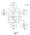
- FIG. 6is a view of a memory system containing a semiconductor device having a thin film according to the present invention.
- FIG. 7is a view of a wafer containing semiconductor dies, each having a semiconductor device with a thin film of the present invention.
- FIG. 8is a block diagram of a circuit module that has a semiconductor device with a thin film of the present invention.
- FIG. 9is a block diagram of a memory module that has a semiconductor device with a thin film of the present invention.
- FIG. 10is a block diagram of an electronic system that has a semiconductor device with a thin film of the present invention.
- FIG. 11is a block diagram of a memory system that has a semiconductor device with a thin film of the present invention.
- FIG. 12is a block diagram of a computer system that has a semiconductor device with a thin film of the present invention.
- wafer and substrate used in the following descriptioninclude any structure having an exposed surface onto which a layer is deposited according to the present invention, for example to form the integrated circuit (IC) structure.
- substrateis understood to include semiconductor wafers.
- substrateis also used to refer to semiconductor structures during processing, and may include other layers that have been fabricated thereupon.
- Both wafer and substrateinclude doped and undoped semiconductors, epitaxial semiconductor layers supported by a base semiconductor or insulator, as well as other semiconductor structures well known to one skilled in the art.
- the term conductoris understood to include semiconductors, and the term insulator is defined to include any material that is less electrically conductive than the materials referred to as conductors.
- reactors for deposition of filmsare understood by those of ordinary skill in the art of semiconductor fabrication.
- the present inventionmay be practiced on a variety of such reactors without undue experimentation.
- one of ordinary skill in the artwill comprehend the necessary detection, measurement, and control techniques in the art of semiconductor fabrication as well as the more inclusive art of industrial processing for producing films on substrates upon reading the disclosure.
- precursorand “reactant” are used herein to differentiate between a chemical compound that includes a metal component to be deposited on a substrate and a gas which reacts with the compound to deposit the metal component on a wafer.
- This nomenclatureis used herein as a tool to clearly describe the invention as both the “precursor” and the “reactant” chemically react with each other to form the desired film on the substrate. Accordingly, the term “precursor” is not intended to imply a time relationship with the “reactant” unless explicitly described.
- FIG. 1depicts an atomic layer deposition (ALD) process according to the teachings of the present invention.
- a substrateis prepared to receive a compound layer, step 15 . This includes forming required layers, trenches, oxides such as field oxides and other structures on the base surface of a wafer.
- the compound layeris a metal nitride.
- the compound layeris a carbide.
- the compound layeris a boride.
- the compound layeris a fluoride.
- the dielectric layere.g., metal oxide or metal nitride
- the dielectric layeris deposited on the bottom electrode layer according to the teachings of the present invention.
- a top electrode layeris deposited on the dielectric layer.
- the remaining structure for the integrated circuitis then formed.
- the source and drainare formed in the substrate.
- a gate insulator, e.g., metal oxide, layeris formed on the substrate intermediate the source and drain according to the teachings of the present invention.
- the gateis formed on the gate insulator.
- Step 17is the first step in the ALD process.
- a first gasflows into a reaction chamber containing the substrate.
- the first gasis deposited at the surface of the substrate.
- the first gasincludes a first element that forms part of the desired compound.
- the first gasincludes titanium.
- the titaniumis a TiCl 4 gas.
- the first gasincludes tantalum.
- the tantalumis a TaCl 5 gas.
- the first gasincludes aluminum.
- the aluminumis a trimethylaluminum (TMA) gas.
- a second gasflows into the chamber containing the substrate and first gas, step 19 .
- the second gasis deposited at the surface of the substrate.
- the second gasincludes a reactant element that will react with the first gas to deposit a first-element containing layer on the substrate.
- the second gasis activated hydrogen.
- the second gasis not H 2 O.
- the first and second gasesare reacted in an ALD reaction to form a monolayer of metal film, step 21 , in an embodiment.
- the monolayer of metal film formed by the first and second gasesis only about one molecule in thickness.
- the monolayeris an essentially pure layer of the first element. Essentially pure is defined as greater than 99% pure. In a more desirable embodiment, essentially pure is greater than 99.9% pure, plus or minus about 0.1%. In an even more desirable embodiment, essentially pure is greater than 99.99% pure, plus or minus 0.01%.
- the first and second gasesreact to form a layer that is greater than a monolayer.
- the ALD layeris exposed to a reacting gas, step 23 .
- the reacting gasconverts the ALD layer containing the first element into a compound containing the first element and at least a second element from the reacting gas.
- the reacting gasincludes oxygen.
- the oxidizing gasis dioxide (O 2 ).
- the oxidizing gasis ozone (O 3 ).
- the oxidizing gasis nitrogen oxide (N 2 O).
- the oxidizing gasis activated oxide (O*).
- the oxidizing gasconverts the tantalum monolayer to Ta 2 O 5 .
- the metal monolayeris aluminum, then the oxidizing gas converts the aluminum monolayer to lumina (Al 2 O 3 ).
- the processis repeated, step 25 , until the desired thickness of the final layer of the first and second elements is formed.
- the processreturns to step 17 to begin forming another ALD layer or monolayer of a first element, which is then converted, according to the teachings of the present invention.
- the first elementis a metal and the second element is oxygen.
- FIG. 1also shows an embodiment of the present invention in broken line. Steps 15 , 17 , 19 and 21 are the same as described above. This embodiment repeats the ALD steps 17 , 19 , 21 until the ALD layer has the final, desired thickness, step 31 . Thereafter, the ALD deposited layer is converted, step 33 .
- convertingincludes reacting the ALD layer with at least one second element to transform the ALD layer (single element layer) into a compound layer (multiple element layer).
- reactingis oxidizing.
- the first elementis a metal. The process then proceeds, if needed, to step 27 .
- FIG. 2Ashows an ALD process 200 according to the teachings of the present invention.
- ALD process 200begins by initiating an inert purge gas flow through a reactor ( 210 ).
- the purge gasmaintains the chamber at a generally constant pressure.
- the purge gas flowis pulsed, for example only injecting purge gas between other gas pulses.
- purge gasis not used at all, i.e. step 210 is not performed.
- the precursor gas containing a first element, e.g., metal, to be deposited on the substratenow flows into the reaction chamber ( 212 ).
- the metalsinclude, for example, titanium, tantalum, or aluminum.
- the metalscan also include alloys of these metals or other metal that one of ordinary skill would deposit on a substrate.
- the precursor gas flowcontinues until a volume closely adjacent the surface of the substrate on which the metal will be deposited is saturated by the precursor gas ( 214 ).
- the precursor gassaturates the topology of the substrate so that adequate precursor material is adjacent the substrate surface by the precursor gas entering and filling the steps, trenches, and holes.
- One of ordinary skillwill understand the same upon reading the disclosure.
- a substrate having numerous or high aspect stepsmay require a longer precursor gas flow period than a substrate which has few steps or relative low aspect steps
- Precursor gas flowends once the precursor gas saturates adjacent the substrate according to the processing conditions of the present deposition ( 218 ).
- reactant gas flowfor example, activated hydrogen
- Reactant gascontinues to flow into the reaction chamber until the reactant gas saturates the volume adjacent the surface of the substrate on which the substance in the precursor gas will be deposited ( 222 ).
- the precursor gas and the reactant gaschemically react and deposit the desired material in a ALD layer, e.g., monolayer, on the substrate.
- the deposited monolayeris about one atomic layer thick.
- the deposited ALD layeris more than one atomic layer thick.
- the monolayer and the ALD layerare an essentially pure layer of a single element.
- the present processmay continue the purge gas flow while the reactant gas flows into the reaction chamber ( 224 ). Once a sufficient quantity of reaction gas is present to complete the reaction with the precursor to deposit a layer on the substrate, reaction gas flow ends ( 226 ). Purge gas flow may continue to partially flush the residual reaction and precursor gases and the by-product gas of the precursor and reactant reaction from the reaction chamber.
- a converting gasflows into the reaction chamber ( 228 ).
- the converting gasincludes an oxidizing gas.
- the oxidizing gasoxidizes the monolayer, which is a metal, to form a dielectric layer. The oxidation continues until sufficient time has elapsed to oxidize essentially all of the metal monolayer ( 230 ).
- step 232it is determined if the converted layer formed by the previous steps has the desired film thickness. If the converted formed by one or a plurality of the ALD and conversion steps of the present invention has the desired thickness, then the ALD and conversion process of the present invention ends. If purge gas is still flowing, then the purge gas flow ends ( 234 ) usually after the remnants of the precursor, reactant, and by-product gases are purged from the chamber. The process of the present invention terminates at box 236 .
- process terminationmay comprise initiation of further processing and does not necessarily require shutdown of the reactor, e.g. the above sequence of steps can be repeated or additional fabrication steps are performed. While one embodiment of the invention includes all of the above steps, the present invention includes other embodiments which do not include all of the above steps.
- step 232determines that the converted layer has the desired thickness.
- FIG. 2BOne embodiment of the present inventive process is shown in FIG. 2B .
- the processbegins with the flow of an inert purge gas and a precursor gas containing the first element into the reaction chamber.
- the precursor gasflows into the chamber until a sufficient quantity of the element that will form the monolayer is adjacent the substrate as determined by stoichiometry of the particular reaction needed to deposit the desired film on the substrate.
- the precursormust include a certain minimum amount of the first element to be deposited on a wafer and other reactive components that assist in the depositing the first element on the wafer.
- the precursormay flow into the reactor in a quantity greater than determined by the stoichiometry of the reaction. In this embodiment, the precursor gas flow ends followed by a short period of only purge gas flow.
- the reactant gasflows into the chamber until a sufficient quantity of reactant gas is available to react with the precursor at the surface of the substrate to deposit the desired first element film.
- An embodiment of the reactant gasinclude activated H. Like the precursor gas flow, the reactant gas and its flow reaches or exceeds the quantity that is determined by the stoichiometry of the particular reaction. Thereafter, the reactant gas flow stops. After the reactant gas flow stops, the converting gas flows into the reaction chamber.
- the converting gasis an oxidizing gas and the first element monolayer is a metal. Accordingly, the metal monolayer on the substrate is oxidized. Thereafter, the flow of converting gas stops. This process is repeated until a converted film of a desired thickness is deposited on the substrate.
- the converting gasincludes an activated element that reacts with the ALD deposited layer.
- the converting gasincludes an activated oxygen.
- the converting gasincludes activated NH 3 .
- the converting gasincludes activated N 2 O.
- the amounts of the precursor gas, the reactant gas, or the converting gasmeets or exceeds the amount of material required by the stoichiometry of the particular reaction. That is, the amount of precursor, reactant, converting gas flow, in certain embodiments, provides excess mass in the reactor. The excess mass is provided to ensure an adequate reaction at the surface of the wafer. In this embodiment, the ratio of precursor, reactant, or converting components in the gas phase usually is different than the stoichiometry of the film.
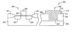
- FIG. 3shows an integrated circuit 300 including a layer formed according to the teachings of the present invention.
- the layeris a dielectric in a capacitor 302 .
- the layeris a gate insulator in a transistor 304 . It is within the scope of the present invention to form the dielectric layer and gate insulator layer for both elements at the same time. It is within the scope of the present invention to form the dielectric layer for the capacitor and the gate insulator layer for the transistor at different times during fabrication.
- Capacitor 302is formed on substrate 305 .
- a trench 307is formed in insulator layer 309 .
- a bottom electrode layer 311is formed in the trench 307 .
- a dielectric layer 313is formed, according to the teachings of the present invention, on the bottom electrode layer 311 .
- a top electrode layer 315is formed on the dielectric layer 313 .
- the transistor 304is also formed on substrate 305 .
- a field oxide 321is formed on the substrate 305 .
- the source and drain regions 323 and 325are doped into the substrate 305 .
- a gate insulator, e.g. an oxide or a nitride, layer 327is formed according to the teachings of the present invention on the substrate 305 intermediate the source and drain regions 323 and 325 .
- a gate 329is formed on the gate insulator layer 327 .
- Dielectric layer or gate insulator layer 313 or 327is a metal oxide material having a composition that includes the form MOx.
- the metal component Mis a refractory metal.
- the refractory metalis tantalum (Ta).
- the refractory metalis titanium (Ti).
- the refractory metalis tungsten (W).
- the refractory metals of chromium (Cr), cobalt (Co), hafnium (Hf), molybdenum (Mo), niobium (Nb), vanadium (V) and zirconium (Zr)are included in some embodiments. Benefits may be derived by matching the metal oxide layer to the adjacent metal-containing electrode.
- the TaOx layer 313 or 327can be grown on a tantalum containing bottom electrode layer.
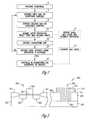
- FIG. 4depicts one embodiment of an atomic layer deposition (ALD) reactor 400 suitable for practicing the present invention.
- ALDatomic layer deposition
- FIG. 4is provided for illustrative purposes and the invention may be practiced with other reactors.
- the embodiment shown in FIG. 4includes a chamber 401 that is a pressure-sealed compartment for mounting a substrate 402 on susceptor 407 .
- Chamber 401is typically manufactured from aluminum and is designed to contain a low-pressure environment around substrate 402 as well as to contain process gases, exhaust gases, and heat or plasma energy within chamber 401 .
- the illustrated substrate 402includes a substrate base 402 A on which are deposited first and second layers 402 B and 402 C.
- Inlet gas manifold 403supplies process gases, for example precursor gases, reactant gases and converting gases, at a controlled flow rates to substrate 402 .
- a source of precursor gas 416is connected to manifold 403 .
- a source of purge gas 417is connected to manifold 403 .
- a source of reactant gas 418is also connected to manifold 403 .
- a source of converting gas 419is also connected to manifold 403 .
- Carrier gasessuch as helium, argon or nitrogen, may also be supplied in conjunction with the gases supplied by the manifold as is known and understood by one of ordinary skill in the art.
- Chamber 401also incorporates a pumping system (not shown) for exhausting spent gases from chamber 401 through exhaust port 404 .
- ALD reactor 400includes means for supplying energy to the reactable constituents or compounds in the process gases in chamber 401 on the surface of the substrate 402 .
- the supplied energycauses the reactable constituents to react or decompose and deposit a thin film onto an upper surface of substrate 402 .
- the supplied energyincludes thermal energy supplied by heat lamps 406 .
- lamps 406are positioned in the base of chamber 401 .
- Heat lamps 406emit a significant amount of near-infra red radiation that passes through susceptor 407 to heat substrate 402 .
- susceptor 407is heated by heat lamps 406 and substrate 402 is heated by conduction from susceptor 407 .
- the heat lamps 406may be placed at alternate locations according to the parameters of the specific deposition process being performed according to the present invention.
- RF generator 408creates a RF field between substrate 402 and an anode.
- susceptor 407is grounded while the RF signal is applied to a process gas manifold 409 .
- Alternative and equivalent ALD reactor designswill be understood by reading the disclosure.
- An RF anodemay be provided separately (not shown) and process gas manifold 409 may be electrically isolated from the RF supply. For example, the RF signal is applied to susceptor 407 and process gas manifold 409 is grounded.
- the energy sources 406 and 408are intended to provide sufficient reaction energy in a region near the surface of substrate 402 to cause decomposition and/or reaction of the constituents of the present gas to deposit the first element, e.g., the metal species, in the process gases onto a surface of the substrate.
- the first elemente.g., the metal species
- One embodimentincludes plasma reactors because these allow film deposition at lower temperatures and are used in the semiconductor industry. However, some reactant constituents in the process gases may deposit at low temperatures using only thermal energy or other energy sources. Hence, the invention encompasses reactor designs using any energy source including either thermal heating, RF plasma, or the like.
- ALD reactor 400is illustrated as a single wafer reactor, but it should be understood that the invention is applicable to batch reactors.
- ALD reactor 400includes associated control apparatus (not shown) for detecting, measuring and controlling process conditions within ALD reactor 400 .
- Associated control apparatusinclude, as examples, temperature sensors, pressure transducers, flow meters and control valves.
- Associated control apparatusfurther include other devices suitable for the detection, measurement and control of the various process conditions described herein.
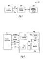
- FIG. 5represents an ALD system 500 suitable for practicing the invention.
- ALD system 500contains the ALD reactor 400 and a control system 510 .
- ALD reactor 400 and control system 510are in communication such that process information is passed from ALD reactor 400 to control system 510 through communication line 520 , and process control information is passed from control system 510 to ALD reactor 400 through communication line 530 .
- communication lines 520 and 530may represent only one physical line, in which communications are bidirectional.
- the control system 510includes, integrally or separable therefrom, a machine readable media 535 which contains instructions for performing the present invention.
- Media 535may be an electrical, magnetic, optical, mechanical, etc. storage device that stores instructions that are read by control system 510 .
- Such storage devicesinclude magnetic disks and tape, optical disks, computer memory, etc.
- Control system 510may also include a processor (not shown) for issuing instructions to control reactor 400 based upon instructions read from machine readable media 535 .
- FIG. 6is a simplified block diagram of a memory device 600 according to one embodiment of the invention.
- the memory device 600includes an array of memory cells 602 , address decoder 604 , row access circuitry 606 , column access circuitry 608 , control circuitry 610 , and Input/Output circuit 612 .
- the memoryis operably coupled to an external microprocessor 614 , or memory controller for memory accessing.
- the memory device 600receives control signals from the processor 614 , such as WE*, RAS* and CAS* signals.
- the memory device 600stores data which is accessed via I/O lines. It will be appreciated by those skilled in the art that additional circuitry and control signals can be provided, and that the memory device of FIG. 6 has been simplified to help focus on the invention.
- At least one of the memory cells or associated circuitryhas an integrated circuit structure or element in accordance with the present invention, e.g., a metal oxide layer formed according to the present invention.
- DRAMDynamic Random Access Memory
- the inventionis equally applicable to any size and type of memory circuit and is not intended to be limited to the DRAM described above.
- Other alternative types of devicesinclude SRAM (Static Random Access Memory) or Flash memories.
- the DRAMcould be a synchronous DRAM commonly referred to as SGRAM (Synchronous Graphics Random Access Memory), SDRAM (Synchronous Dynamic Random Access Memory), SDRAM II, and DDR SDRAM (Double Data Rate SDRAM), as well as Synchlink or Rambus DRAMs and other emerging DRAM technologies.
- a semiconductor die 710is produced from a wafer 700 .
- a die 710is an individual pattern, typically rectangular, on a substrate or wafer 700 that contains circuitry, or integrated circuit devices, to perform a specific function.
- a semiconductor wafer 700will typically contain a repeated pattern of such dies 710 containing the same functionality.
- Die 710contains circuitry for the inventive memory device, as discussed above. Die 710 may further contain additional circuitry to extend to such complex devices as a monolithic processor with multiple functionality.
- Die 710is typically packaged in a protective casing (not shown) with leads extending therefrom (not shown) providing access to the circuitry of the die for unilateral or bilateral communication and control.
- Each die 710includes at least one ALD deposited and converted layer, e.g., a metal oxide, according to the present invention.
- circuit module 800may be a combination of dies 710 representing a variety of functions, or a combination of dies 710 containing the same functionality.
- One or more dies 710 of circuit module 800contain at least one ALD deposited and converted layer, e.g., a metal oxide, in accordance with the present invention.
- Circuit module 800may be a subcomponent of a variety of electronic systems, such as a clock, a television, a cell phone, a personal computer, an automobile, an industrial control system, an aircraft and others. Circuit module 800 will have a variety of leads 810 extending therefrom and coupled to the dies 710 providing unilateral or bilateral communication and control.
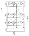
- FIG. 9shows one embodiment of a circuit module as memory module 900 .
- Memory module 900contains multiple memory devices 910 contained on support 915 , the number generally depending upon the desired bus width and the desire for parity.
- Memory module 900accepts a command signal from an external controller (not shown) on a command link 920 and provides for data input and data output on data links 930 .
- the command link 920 and data links 930are connected to leads 940 extending from the support 915 .
- Leads 940are shown for conceptual purposes and are not limited to the positions shown in FIG. 9 .
- At least one of the memory devices 910contains a ALD deposited and converted layer, e.g., a metal oxide, according to the present invention.
- FIG. 10shows one embodiment of an electronic system 1000 containing one or more circuit modules 800 .
- Electronic system 1000generally contains a user interface 1010 .
- User interface 1010provides a user of the electronic system 1000 with some form of control or observation of the results of the electronic system 1000 .
- Some examples of user interface 1010include the keyboard, pointing device, monitor or printer of a personal computer; the tuning dial, display or speakers of a radio; the ignition switch, gauges or gas pedal of an automobile; and the card reader, keypad, display or currency dispenser of an automated teller machine, or other human-machine interfaces.
- User interface 1010may further describe access ports provided to electronic system 1000 . Access ports are used to connect an electronic system to the more tangible user interface components previously exemplified.
- One or more of the circuit modules 800may be a processor providing some form of manipulation, control or direction of inputs from or outputs to user interface 1010 , or of other information either preprogrammed into, or otherwise provided to, electronic system 1000 .
- electronic system 1000will often be associated with certain mechanical components (not shown) in addition to circuit modules 800 and user interface 1010 .
- the one or more circuit modules 800 in electronic system 1000can be replaced by a single integrated circuit.
- electronic system 1000may be a subcomponent of a larger electronic system.
- at least one of the memory modules 800contains a ALD deposited and converted layer, e.g., a metal oxide, according to the present invention.
- FIG. 11shows one embodiment of an electronic system as memory system 1100 .
- Memory system 1100contains one or more memory modules 900 and a memory controller 1110 .
- the memory modules 900each contain one or more memory devices 910 .
- At least one of memory devices 910contain ALD deposited and converted layer, e.g., a metal oxide, according to the present invention.
- Memory controller 1110provides and controls a bidirectional interface between memory system 1100 and an external system bus 1120 .
- Memory system 1100accepts a command signal from the external bus 1120 and relays it to the one or more memory modules 900 on a command link 1130 .
- Memory system 1100provides for data input and data output between the one or more memory modules 900 and external system bus 1120 on data links 1140 .
- FIG. 12shows a further embodiment of an electronic system as a computer system 1200 .
- Computer system 1200contains a processor 1210 and a memory system 1100 housed in a computer unit 1205 .
- Computer system 1200is but one example of an electronic system containing another electronic system, i.e., memory system 900 , as a subcomponent.
- Computer system 1200optionally contains user interface components. Depicted in FIG. 12 are a keyboard 1220 , a pointing device 1230 , a monitor 1240 , a printer 1250 and a bulk storage device 1260 . It will be appreciated that other components are often associated with computer system 1200 such as modems, device driver cards, additional storage devices, etc.
- processor 1210 and memory system 1100 of computer system 1200can be incorporated on a single integrated circuit. Such single package processing units reduce the communication time between the processor and the memory circuit. It will be appreciated that at least one of the processor 1210 and memory system 1100 contains a ALD deposited and converted layer, e.g., a metal oxide, according to the present invention.
- ALDatomic layer deposition
- a first monolayere.g., metal layer
- convertinge.g., oxidizing the metal layer to form a metal oxide.
- the present inventionis also applicable to forming other elemental layers in an integrated circuit. For example, a layer is deposited using ALD and then the layer is nitrided. Thus, the layer is now a nitride layer. The process is repeated until the nitride layer has the desired thickness.
- the layeris subjected to boron and thus becomes a boride layer.
- the above described stepsare performed with the boron replacing the oxygen.
- the layeris subjected to carbon and thus becomes a carbide layer.
- the above described stepsare performed with the carbon replacing the oxygen.
- the layeris subjected to fluorine and thus becomes a fluoride layer.
- the above described stepsare performed with the fluorine replacing the oxygen.
- the layeris subjected to phosphorus and thus becomes a phosphide layer.
- the above described stepsare performed with the phosphorus replacing the oxygen.
- the present inventionproduces mixed phase films.
- the mixed phase filmsinclude more than one base element.
- the first elementis deposited using ALD in an ALD layer, monolayer or atomic layer. It is then converted according to the teachings of the present invention.
- a second elementis deposited using ALD in a monolayer or atomic layer.
- the second element layeris then converted according to the teachings of the present invention.
- the first or second elementis an alloy of a metal. Consequently, mixed element film is formed by sequentially depositing and converting the first element and the subsequent element(s). It will be appreciated that the present method is adaptable to higher orders of elements in the film, wherein a third element is deposited and converted, and an nth element is deposited and converted.
- An example of such an ALD layer that is converted according to the teachings of the present inventioninclude, but are not limited to, titanium and silicon in the base film.
- One embodimentwould be formed by depositing both titanium and silicon by ALD then converting one or both according to the teachings of the present invention to form TiO 2 SiN x .
- Titaniumis deposited in an ALD layer, such as a monolayer, using ALD and then converted according to the teachings herein. Silicon is deposited and then converted either before or after the titanium. Accordingly, the film that is formed alternates depositing and converting the titanium and the silicon.
- An embodiment according to the teachings of the present inventionincludes depositing titanium and silicon by ALD and then converting both elements with oxygen to form TiO x SiO x .
- the titaniumis first deposited, then oxidized.
- the siliconis then deposited, then converted using oxygen.
- the titanium and siliconare both deposited by ALD, then both converted by oxidizing the titanium and silicon.
- either the TiO x or SiO xis deposited according to ALD and the other of the TiO x or SiO x is deposited by ALD and then converted according to the teachings of the present invention.
- An embodiment according to the teachings of the present inventionincludes depositing titanium by ALD and then converting the titanium using both oxygen and nitrogen to form a TiO x TiN layer.
- either the TiO x or TiNis deposited according to ALD and the other of the TiO x or TiN is deposited by ALD and then converted according to the teachings of the present invention.
- An embodiment according to the teachings of the present inventionincludes depositing silicon by ALD and then converting the silicon using both oxygen and nitrogen to form a SiO x SiN layer.
- either the SiN or SiO xis deposited according to ALD and the other of the SiN or SiO x is deposited by ALD and then converted according to the teachings of the present invention.
- An embodiment according to the teachings of the present inventionincludes depositing tantalum and silicon by ALD and converting tantalum with nitrogen to form TaNSi.
- the tantalumis deposited, then converted with nitrogen.
- the siliconis deposited by ALD.
- the present inventionforms TaNTaSi.
- An embodiment according to the teachings of the present inventionincludes depositing aluminum and titanium by ALD and then converting both elements with oxygen to form AlO 3 TiO 2 .
- the titaniumis first deposited, then oxidized.
- the aluminumis then deposited, then converted using oxygen.
- the titanium and aluminumare both deposited by ALD, then both converted by oxidizing the titanium and aluminum.
- either the TiO 2 or AlO 3is deposited according to ALD and the other of the TiO 2 or AlO 3 is deposited by ALD and then converted according to the teachings of the present invention.
- the present inventionincludes methods of forming alloys or mixed element films and converting the alloy or mixed element films according to the teachings of the present invention.
- Some of the above embodimentdescribe specific elements that are deposited and converted or deposited in combination with elements that are converted according to the teachings of the present invention. It will be recognized that the order and methods described in conjunction with these specific elements are adaptable to other elements that are used to form layers in integrated circuits.
- the present inventionprovides novel structures and methods for fabrication of thin films on substrates.
- the novel fabrication method of the present inventionforms a first layer of a single element by ALD and then converts the first layer to a second layer having two constituent elements.
- the first layeris formed by atomic layer deposition and then converted.
- each first layer produced during an atomic layer depositionis converted before a subsequent first layer is deposited on the prior converted sub-layer.
- conversionis oxidation and the first layer is a metal.
- each metal sub-layer produced during an atomic layer depositionis oxidized before a subsequent metal sub-layer is deposited on the prior oxidized metal sub-layer.
- each sub-layeris formed at a molecular level by atomic layer deposition and thus has a high quality. Quality includes low impurity and low defects.
- Each sub-layeris then oxidized. Accordingly, the oxidation is throughout the sub-layer and prevents non-oxidized areas in the sub-layer. The process is then repeated to until the oxidized sub-layers produce a film or layer that has the desired thickness.
Landscapes
- Engineering & Computer Science (AREA)
- Chemical & Material Sciences (AREA)
- Physics & Mathematics (AREA)
- Condensed Matter Physics & Semiconductors (AREA)
- Power Engineering (AREA)
- Microelectronics & Electronic Packaging (AREA)
- Computer Hardware Design (AREA)
- Manufacturing & Machinery (AREA)
- General Physics & Mathematics (AREA)
- Mechanical Engineering (AREA)
- Organic Chemistry (AREA)
- Metallurgy (AREA)
- Materials Engineering (AREA)
- Chemical Kinetics & Catalysis (AREA)
- General Chemical & Material Sciences (AREA)
- Electromagnetism (AREA)
- Plasma & Fusion (AREA)
- Chemical Vapour Deposition (AREA)
- Formation Of Insulating Films (AREA)
- Semiconductor Memories (AREA)
Abstract
Description
- This application is a Divisional of U.S. application Ser. No. 10/137,058, filed May 2, 2002 which is incorporated herein by reference.
- The present invention relates to deposition techniques and, more particularly, to deposition techniques for forming thin films on wafers or substrates and then converting the films into a different another composition.
- Integrated circuits (IC) are often fabricated with one or more semiconductor devices, which may include diodes, capacitors, and different varieties of transistors. These devices are generally fabricated by creating thin films of various materials, e.g. metals, semiconductors or insulators, upon a substrate or semiconductor wafer. Wafer and substrate are used interchangeably to refer to semiconductor structures during processing, and may include other layers that have been fabricated thereon. The physical characteristics and tightly controlled placement of films on a substrate will define the performance of the semiconductor device and its surrounding circuitry. Many semiconductor devices require a dielectric layer that must be reliable. Specifically, the dielectric layer must be essentially free from defects that cause shorting through the dielectric layer. Oxides and nitrides are used to form dielectric layers in semiconductor devices.
- One process for forming metal oxide thin films on semiconductor wafers is chemical vapor deposition (“CVD”). CVD is used to form a thin film of a desired material from a reaction of vapor-phase chemicals containing the chemical constituents of the material. CVD processes operate by confining one or more semiconductor wafers in a reaction chamber. The chamber is filled with one or more gases that surround the wafer. The gases for the deposition of metal oxides includes a metal precursor and a reactant gas, e.g. water vapor, to be introduced into the chamber at the same time. Energy is supplied within the chamber and particularly to the reactant gases near the wafer surface. A typical energy is heat applied to the substrate. The energy activates the reactant gas chemistry to deposit a film from the gases onto the heated substrate. Such chemical vapor deposition of a solid onto a surface involves a heterogeneous surface reaction of the gaseous species that adsorb onto the surface. The rate of film growth and the quality of the film depend on the process conditions. Unfortunately, the metal precursor and the reactant gas also react during the gas phase remote from the substrate. Such a gas phase reaction produces contaminants and/or involve a significant quantity of precursor so that an insufficient amount is available for deposition on the substrate. As a result, the gas phase reaction may become dominant and the thin film coverage is poor. That is, pinholes may be formed in the resulting metal oxide layer. Moreover, using water (H2O) gas as the reactant gas results in impurities, such as hydroxide (OH), remaining in the resulting metal oxide layer.
- Semiconductor fabrication continues to advance, requiring finer dimensional tolerances and control. Modem integrated circuit design has advanced to the point where line width may be 0.25 microns or less. As a result, repeatability and uniformity of processes and their results is becoming increasingly important. Generally, it is desired to have thin films deposited on the wafer to save space. Yet reducing the thickness of films can result in pinholes and in less mechanical strength.
- Another development in the field of thin film technology for coating substrates is atomic layer deposition (ALD). A description of ALD is set forth in U.S. Pat. No. 5,879,459, which is herein incorporated by reference in its entirety. ALD operates by confining a wafer in a reaction chamber at a typical temperature of less than 300 degrees C. Precursor gas is pulsed into the chamber, wherein the pulsed precursor forms a monolayer on the substrate by chemisorption. The low temperature limits the bonding of the precursor to chemisorption, thus only a single layer, usually only one atom or molecule thick, is grown on the wafer. Each pulse is separated by a purge pulse which completely purges all of the precursor gas from the chamber before the next pulse of precursor gas begins. Each injection of precursor gas provides a new single atomic layer on the previously deposited layers to form a layer of film. Obviously, this significantly increases the time it takes to depose a layer having adequate thickness on the substrate. As a numerical example, ALD has a typical deposition rate of about 100 Å/min and CVD has a typical deposition rate of about 1000 Å/min. For at least this reason, ALD has not met with widespread commercial acceptance.
- In light of the foregoing, there is a need for fabrication of thin films which are thinner and have a reduced number of defects.
- The above mentioned problems with thin film fabrication techniques are addressed by the present invention and will be understood by reading and studying the following specification. Systems and methods are provided for fabricating thin films on substrates. The fabrication technique of the present invention grows a thin film by atomic layer deposition and then converts the film to produce a thin film having a different composition than the ALD deposited film. In an embodiment, each ALD thin film is converted before a subsequent ALD film is deposited. In one embodiment of the invention, a metal film is deposited by ALD. The metal film is then oxidized to produce a metal oxide film. In an embodiment, the metal is aluminum. In an embodiment, the metal is titanium. In an embodiment, the metal is tantalum.
- In an embodiment, the thin film formed by atomic layer deposition is converted from an essentially pure metal film to a compound film that includes the metal and at least one second element. In an embodiment, the second element is oxygen. In an embodiment, the compound film is an oxide. In an embodiment, the second element is nitrogen. In an embodiment, the compound film is a nitride. In an embodiment, the second element is boron. In an embodiment, the compound film is a boride. In an embodiment, the second element is carbon. In an embodiment, the compound film is a carbide. In an embodiment, the second element is fluorine. In an embodiment, the compound film is a fluoride.
- In an embodiment, a laminate or compound layer having at least two compounds in the layer is formed. The first element layer is deposited by ALD. This layer is then converted to a compound. A second element layer is deposited by ALD. This layer is then converted to a compound. In an embodiment, both the first and second elements are deposited by ALD and then both elements are converted. In an embodiment, one of the first element layer and second element layer is deposited by ALD and not converted. If the one layer includes a compound, then it is deposited by ALD in its compound form. The other of the first element layer and the second element layer is converted.
- Additional embodiments of the invention include deposition devices and systems for forming metal oxide films on substrates, and machine readable media having fabrication instructions stored thereon, all according to the teachings of the present invention as described herein.
- These and other embodiments, aspects, advantages, and features of the present invention will be set forth in part in the description which follows, and in part will become apparent to those skilled in the art by reference to the following description of the invention and referenced drawings or by practice of the invention. The aspects, advantages, and features of the invention are realized and attained by means of the instrumentalities, procedures, and combinations particularly pointed out in the appended claims.
FIG. 1 is a flow chart of the deposition process of an embodiment of the invention.FIG. 2A is a flowchart of the deposition process of an embodiment of the invention.FIG. 2B is a time graph of a deposition process of the present invention.FIG. 3 is a view of a thin film of the present invention as a dielectric layer in a capacitor and as a gate layer in a transistor.FIG. 4 is a view of a reactor for use with the process of the present invention.FIG. 5 is a view of a reactor system for use with the process of the present invention.FIG. 6 is a view of a memory system containing a semiconductor device having a thin film according to the present invention.FIG. 7 is a view of a wafer containing semiconductor dies, each having a semiconductor device with a thin film of the present invention.FIG. 8 is a block diagram of a circuit module that has a semiconductor device with a thin film of the present invention.FIG. 9 is a block diagram of a memory module that has a semiconductor device with a thin film of the present invention.FIG. 10 is a block diagram of an electronic system that has a semiconductor device with a thin film of the present invention.FIG. 11 is a block diagram of a memory system that has a semiconductor device with a thin film of the present invention.FIG. 12 is a block diagram of a computer system that has a semiconductor device with a thin film of the present invention.- In the following detailed description of the invention, reference is made to the accompanying drawings which form a part hereof, and in which is shown, by way of illustration, specific embodiments in which the invention may be practiced. These embodiments are described in sufficient detail to enable those skilled in the art to practice the invention. Other embodiments may be utilized and structural, logical, and electrical changes may be made without departing from the scope of the present invention. The terms wafer and substrate used in the following description include any structure having an exposed surface onto which a layer is deposited according to the present invention, for example to form the integrated circuit (IC) structure. The term substrate is understood to include semiconductor wafers. The term substrate is also used to refer to semiconductor structures during processing, and may include other layers that have been fabricated thereupon. Both wafer and substrate include doped and undoped semiconductors, epitaxial semiconductor layers supported by a base semiconductor or insulator, as well as other semiconductor structures well known to one skilled in the art. The term conductor is understood to include semiconductors, and the term insulator is defined to include any material that is less electrically conductive than the materials referred to as conductors. The following detailed description is, therefore, not to be taken in a limiting sense, and the scope of the present invention is defined only by the appended claims, along with the full scope of equivalents to which such claims are entitled.
- According to the teachings of the present invention, fabrication of films on substrates, devices and systems for such fabrication, media containing instructions therefor, and integrated circuits produced according to the present invention are described.
- The use, construction and fundamental operation of reactors for deposition of films are understood by those of ordinary skill in the art of semiconductor fabrication. The present invention may be practiced on a variety of such reactors without undue experimentation. Furthermore, one of ordinary skill in the art will comprehend the necessary detection, measurement, and control techniques in the art of semiconductor fabrication as well as the more inclusive art of industrial processing for producing films on substrates upon reading the disclosure.
- It will be understood that the terms “precursor” and “reactant” are used herein to differentiate between a chemical compound that includes a metal component to be deposited on a substrate and a gas which reacts with the compound to deposit the metal component on a wafer. This nomenclature is used herein as a tool to clearly describe the invention as both the “precursor” and the “reactant” chemically react with each other to form the desired film on the substrate. Accordingly, the term “precursor” is not intended to imply a time relationship with the “reactant” unless explicitly described.
- Applicant hereby incorporates by reference copending U.S. patent application Ser. No. 09/782,207, which is assigned to the assignee of the present application.
FIG. 1 depicts an atomic layer deposition (ALD) process according to the teachings of the present invention. A substrate is prepared to receive a compound layer,step 15. This includes forming required layers, trenches, oxides such as field oxides and other structures on the base surface of a wafer. In an embodiment, the compound layer is a metal nitride. In an embodiment, the compound layer is a carbide. In an embodiment, the compound layer is a boride. In an embodiment, the compound layer is a fluoride. When depositing a dielectric layer for a capacitor, a field insulator is formed on the wafer. The field insulator is etched to form a trench. A bottom electrode layer is deposited in the trench. Thereafter, the dielectric layer, e.g., metal oxide or metal nitride, is deposited on the bottom electrode layer according to the teachings of the present invention. After the dielectric is formed a top electrode layer is deposited on the dielectric layer. The remaining structure for the integrated circuit is then formed. When depositing a gate oxide for a transistor, the source and drain are formed in the substrate. A gate insulator, e.g., metal oxide, layer is formed on the substrate intermediate the source and drain according to the teachings of the present invention. Thereafter, the gate is formed on the gate insulator. The remaining structure for the integrated circuit is then formed.Step 17 is the first step in the ALD process. A first gas flows into a reaction chamber containing the substrate. The first gas is deposited at the surface of the substrate. The first gas includes a first element that forms part of the desired compound. In an embodiment, the first gas includes titanium. In an embodiment, the titanium is a TiCl4gas. In an embodiment, the first gas includes tantalum. In an embodiment, the tantalum is a TaCl5gas. In an embodiment, the first gas includes aluminum. In an embodiment, the aluminum is a trimethylaluminum (TMA) gas. A second gas flows into the chamber containing the substrate and first gas,step 19. The second gas is deposited at the surface of the substrate. The second gas includes a reactant element that will react with the first gas to deposit a first-element containing layer on the substrate. In an embodiment, the second gas is activated hydrogen. In an embodiment, the second gas is not H2O. The first and second gases are reacted in an ALD reaction to form a monolayer of metal film,step 21, in an embodiment. In this embodiment of ALD, the monolayer of metal film formed by the first and second gases is only about one molecule in thickness. The monolayer is an essentially pure layer of the first element. Essentially pure is defined as greater than 99% pure. In a more desirable embodiment, essentially pure is greater than 99.9% pure, plus or minus about 0.1%. In an even more desirable embodiment, essentially pure is greater than 99.99% pure, plus or minus 0.01%. In another embodiment of ALD, the first and second gases react to form a layer that is greater than a monolayer. After the ALD layer is formed on the substrate, the ALD layer is exposed to a reacting gas,step 23. The reacting gas converts the ALD layer containing the first element into a compound containing the first element and at least a second element from the reacting gas. In an embodiment, the reacting gas includes oxygen. In an embodiment, the oxidizing gas is dioxide (O2). In an embodiment, the oxidizing gas is ozone (O3). In an embodiment, the oxidizing gas is nitrogen oxide (N2O). In an embodiment, the oxidizing gas is activated oxide (O*). When the metal monolayer is titanium, then the oxidizing gas converts the titanium monolayer to ATiO3, where A denotes Ba or Sr or both. When the metal monolayer is tantalum, then the oxidizing gas converts the tantalum monolayer to Ta2O5. When the metal monolayer is aluminum, then the oxidizing gas converts the aluminum monolayer to lumina (Al2O3). The process is repeated,step 25, until the desired thickness of the final layer of the first and second elements is formed. The process returns to step17 to begin forming another ALD layer or monolayer of a first element, which is then converted, according to the teachings of the present invention. In an embodiment, the first element is a metal and the second element is oxygen. After the final layer has the desired thickness, then additional integrated circuit fabrication processes are performed on the substrate as needed,step 27.FIG. 1 also shows an embodiment of the present invention in broken line.Steps step 31. Thereafter, the ALD deposited layer is converted,step 33. In an embodiment, converting includes reacting the ALD layer with at least one second element to transform the ALD layer (single element layer) into a compound layer (multiple element layer). In an embodiment, reacting is oxidizing. In an embodiment, the first element is a metal. The process then proceeds, if needed, to step27.FIG. 2A shows anALD process 200 according to the teachings of the present invention.ALD process 200, in the illustrated embodiment, begins by initiating an inert purge gas flow through a reactor (210). The purge gas maintains the chamber at a generally constant pressure. In one embodiment of the present invention the purge gas flow is pulsed, for example only injecting purge gas between other gas pulses. In another embodiment, purge gas is not used at all, i.e.step 210 is not performed.- The precursor gas containing a first element, e.g., metal, to be deposited on the substrate now flows into the reaction chamber (212). The metals include, for example, titanium, tantalum, or aluminum. The metals can also include alloys of these metals or other metal that one of ordinary skill would deposit on a substrate. The precursor gas flow continues until a volume closely adjacent the surface of the substrate on which the metal will be deposited is saturated by the precursor gas (214). According to the teachings of the present invention, the precursor gas saturates the topology of the substrate so that adequate precursor material is adjacent the substrate surface by the precursor gas entering and filling the steps, trenches, and holes. One of ordinary skill will understand the same upon reading the disclosure. The precursor gas flow, as well as purge gas flow if present, continues until the required saturation occurs depending on the processing conditions dictated by the type of substrate and precursor gas, and the topology of the substrate (216). A substrate having numerous or high aspect steps may require a longer precursor gas flow period than a substrate which has few steps or relative low aspect steps
- Precursor gas flow ends once the precursor gas saturates adjacent the substrate according to the processing conditions of the present deposition (218). After or substantially at the same time precursor gas flow is stopped, reactant gas flow (for example, activated hydrogen) begins in the reaction chamber (220). Reactant gas continues to flow into the reaction chamber until the reactant gas saturates the volume adjacent the surface of the substrate on which the substance in the precursor gas will be deposited (222). The precursor gas and the reactant gas chemically react and deposit the desired material in a ALD layer, e.g., monolayer, on the substrate. In an embodiment, the deposited monolayer is about one atomic layer thick. In an embodiment, the deposited ALD layer is more than one atomic layer thick. The monolayer and the ALD layer are an essentially pure layer of a single element.
- The present process may continue the purge gas flow while the reactant gas flows into the reaction chamber (224). Once a sufficient quantity of reaction gas is present to complete the reaction with the precursor to deposit a layer on the substrate, reaction gas flow ends (226). Purge gas flow may continue to partially flush the residual reaction and precursor gases and the by-product gas of the precursor and reactant reaction from the reaction chamber. A converting gas flows into the reaction chamber (228). The converting gas includes an oxidizing gas. The oxidizing gas oxidizes the monolayer, which is a metal, to form a dielectric layer. The oxidation continues until sufficient time has elapsed to oxidize essentially all of the metal monolayer (230). If the monolayer is not sufficiently oxidized the process continues flowing the oxidizing gas to the metal monolayer. Once the monolayer is sufficiently converted, e.g., oxidized, then the process proceeds to step232. At
step 232, it is determined if the converted layer formed by the previous steps has the desired film thickness. If the converted formed by one or a plurality of the ALD and conversion steps of the present invention has the desired thickness, then the ALD and conversion process of the present invention ends. If purge gas is still flowing, then the purge gas flow ends (234) usually after the remnants of the precursor, reactant, and by-product gases are purged from the chamber. The process of the present invention terminates atbox 236. The reader should note that process termination may comprise initiation of further processing and does not necessarily require shutdown of the reactor, e.g. the above sequence of steps can be repeated or additional fabrication steps are performed. While one embodiment of the invention includes all of the above steps, the present invention includes other embodiments which do not include all of the above steps. - If the desired thickness of the layer has not been achieved (222), then the process returns to step210 or step212 and begins another cycle. The process then reiterates the above sequence/process until
step 232 determines that the converted layer has the desired thickness. - One embodiment of the present inventive process is shown in
FIG. 2B . The process begins with the flow of an inert purge gas and a precursor gas containing the first element into the reaction chamber. The precursor gas flows into the chamber until a sufficient quantity of the element that will form the monolayer is adjacent the substrate as determined by stoichiometry of the particular reaction needed to deposit the desired film on the substrate. The precursor must include a certain minimum amount of the first element to be deposited on a wafer and other reactive components that assist in the depositing the first element on the wafer. The precursor may flow into the reactor in a quantity greater than determined by the stoichiometry of the reaction. In this embodiment, the precursor gas flow ends followed by a short period of only purge gas flow. The reactant gas flows into the chamber until a sufficient quantity of reactant gas is available to react with the precursor at the surface of the substrate to deposit the desired first element film. An embodiment of the reactant gas include activated H. Like the precursor gas flow, the reactant gas and its flow reaches or exceeds the quantity that is determined by the stoichiometry of the particular reaction. Thereafter, the reactant gas flow stops. After the reactant gas flow stops, the converting gas flows into the reaction chamber. In an embodiment, the converting gas is an oxidizing gas and the first element monolayer is a metal. Accordingly, the metal monolayer on the substrate is oxidized. Thereafter, the flow of converting gas stops. This process is repeated until a converted film of a desired thickness is deposited on the substrate. - The converting gas includes an activated element that reacts with the ALD deposited layer. In an embodiment, the converting gas includes an activated oxygen. In an embodiment, the converting gas includes activated NH3. In an embodiment, the converting gas includes activated N2O.
- The amounts of the precursor gas, the reactant gas, or the converting gas meets or exceeds the amount of material required by the stoichiometry of the particular reaction. That is, the amount of precursor, reactant, converting gas flow, in certain embodiments, provides excess mass in the reactor. The excess mass is provided to ensure an adequate reaction at the surface of the wafer. In this embodiment, the ratio of precursor, reactant, or converting components in the gas phase usually is different than the stoichiometry of the film.
FIG. 3 shows anintegrated circuit 300 including a layer formed according to the teachings of the present invention. The layer is a dielectric in acapacitor 302. The layer is a gate insulator in atransistor 304. It is within the scope of the present invention to form the dielectric layer and gate insulator layer for both elements at the same time. It is within the scope of the present invention to form the dielectric layer for the capacitor and the gate insulator layer for the transistor at different times during fabrication.Capacitor 302 is formed onsubstrate 305. In an embodiment, atrench 307 is formed ininsulator layer 309. Abottom electrode layer 311 is formed in thetrench 307. Adielectric layer 313 is formed, according to the teachings of the present invention, on thebottom electrode layer 311. Atop electrode layer 315 is formed on thedielectric layer 313. Thetransistor 304 is also formed onsubstrate 305. Afield oxide 321 is formed on thesubstrate 305. The source and drainregions substrate 305. A gate insulator, e.g. an oxide or a nitride,layer 327 is formed according to the teachings of the present invention on thesubstrate 305 intermediate the source and drainregions gate 329 is formed on thegate insulator layer 327.- Dielectric layer or
gate insulator layer TaOx layer FIG. 4 depicts one embodiment of an atomic layer deposition (ALD)reactor 400 suitable for practicing the present invention.FIG. 4 is provided for illustrative purposes and the invention may be practiced with other reactors. The embodiment shown inFIG. 4 includes achamber 401 that is a pressure-sealed compartment for mounting asubstrate 402 onsusceptor 407.Chamber 401 is typically manufactured from aluminum and is designed to contain a low-pressure environment aroundsubstrate 402 as well as to contain process gases, exhaust gases, and heat or plasma energy withinchamber 401. The illustratedsubstrate 402 includes asubstrate base 402A on which are deposited first andsecond layers Inlet gas manifold 403 supplies process gases, for example precursor gases, reactant gases and converting gases, at a controlled flow rates tosubstrate 402. A source ofprecursor gas 416 is connected tomanifold 403. A source ofpurge gas 417 is connected tomanifold 403. A source ofreactant gas 418 is also connected tomanifold 403. A source of convertinggas 419 is also connected tomanifold 403. Carrier gases, such as helium, argon or nitrogen, may also be supplied in conjunction with the gases supplied by the manifold as is known and understood by one of ordinary skill in the art.Chamber 401 also incorporates a pumping system (not shown) for exhausting spent gases fromchamber 401 throughexhaust port 404.ALD reactor 400 includes means for supplying energy to the reactable constituents or compounds in the process gases inchamber 401 on the surface of thesubstrate 402. The supplied energy causes the reactable constituents to react or decompose and deposit a thin film onto an upper surface ofsubstrate 402. In one embodiment, the supplied energy includes thermal energy supplied byheat lamps 406. In the illustrated example,lamps 406 are positioned in the base ofchamber 401.Heat lamps 406 emit a significant amount of near-infra red radiation that passes throughsusceptor 407 toheat substrate 402. Alternatively,susceptor 407 is heated byheat lamps 406 andsubstrate 402 is heated by conduction fromsusceptor 407. Theheat lamps 406 may be placed at alternate locations according to the parameters of the specific deposition process being performed according to the present invention.- Another embodiment supplies reaction energy by a radio frequency (RF)
generator 408 as shown inFIG. 4 .RF generator 408 creates a RF field betweensubstrate 402 and an anode. In the embodiment shown inFIG. 4 ,susceptor 407 is grounded while the RF signal is applied to aprocess gas manifold 409. Alternative and equivalent ALD reactor designs will be understood by reading the disclosure. An RF anode may be provided separately (not shown) andprocess gas manifold 409 may be electrically isolated from the RF supply. For example, the RF signal is applied tosusceptor 407 andprocess gas manifold 409 is grounded. - In general, the
energy sources substrate 402 to cause decomposition and/or reaction of the constituents of the present gas to deposit the first element, e.g., the metal species, in the process gases onto a surface of the substrate. One of ordinary skill in the art will understand upon reading the disclosure that any one, combination, or equivalent of the above can be employed to provide the necessary reaction energy. - One embodiment includes plasma reactors because these allow film deposition at lower temperatures and are used in the semiconductor industry. However, some reactant constituents in the process gases may deposit at low temperatures using only thermal energy or other energy sources. Hence, the invention encompasses reactor designs using any energy source including either thermal heating, RF plasma, or the like.
ALD reactor 400 is illustrated as a single wafer reactor, but it should be understood that the invention is applicable to batch reactors.- Furthermore,
ALD reactor 400 includes associated control apparatus (not shown) for detecting, measuring and controlling process conditions withinALD reactor 400. Associated control apparatus include, as examples, temperature sensors, pressure transducers, flow meters and control valves. Associated control apparatus further include other devices suitable for the detection, measurement and control of the various process conditions described herein. - One of ordinary skill in the art will comprehend other suitable reactors for practicing the invention described in this application, for example the reactors described in U.S. Pat. Nos. 5,879,459 and 6,305,314, herein incorporated by reference.
FIG. 5 represents anALD system 500 suitable for practicing the invention.ALD system 500 contains theALD reactor 400 and acontrol system 510.ALD reactor 400 andcontrol system 510 are in communication such that process information is passed fromALD reactor 400 to controlsystem 510 throughcommunication line 520, and process control information is passed fromcontrol system 510 toALD reactor 400 throughcommunication line 530. It is noted thatcommunication lines - The
control system 510 includes, integrally or separable therefrom, a machinereadable media 535 which contains instructions for performing the present invention.Media 535 may be an electrical, magnetic, optical, mechanical, etc. storage device that stores instructions that are read bycontrol system 510. Such storage devices include magnetic disks and tape, optical disks, computer memory, etc.Control system 510 may also include a processor (not shown) for issuing instructions to controlreactor 400 based upon instructions read from machinereadable media 535. - Memory Devices
FIG. 6 is a simplified block diagram of amemory device 600 according to one embodiment of the invention. Thememory device 600 includes an array ofmemory cells 602,address decoder 604,row access circuitry 606,column access circuitry 608,control circuitry 610, and Input/Output circuit 612. The memory is operably coupled to anexternal microprocessor 614, or memory controller for memory accessing. Thememory device 600 receives control signals from theprocessor 614, such as WE*, RAS* and CAS* signals. Thememory device 600 stores data which is accessed via I/O lines. It will be appreciated by those skilled in the art that additional circuitry and control signals can be provided, and that the memory device ofFIG. 6 has been simplified to help focus on the invention. At least one of the memory cells or associated circuitry has an integrated circuit structure or element in accordance with the present invention, e.g., a metal oxide layer formed according to the present invention.- It will be understood that the above description of a memory device is intended to provide a general understanding of the memory and is not a complete description of all the elements and features of a specific type of memory, such as DRAM (Dynamic Random Access Memory). Further, the invention is equally applicable to any size and type of memory circuit and is not intended to be limited to the DRAM described above. Other alternative types of devices include SRAM (Static Random Access Memory) or Flash memories. Additionally, the DRAM could be a synchronous DRAM commonly referred to as SGRAM (Synchronous Graphics Random Access Memory), SDRAM (Synchronous Dynamic Random Access Memory), SDRAM II, and DDR SDRAM (Double Data Rate SDRAM), as well as Synchlink or Rambus DRAMs and other emerging DRAM technologies.
- Semiconductor Dies
- With reference to
FIG. 7 , for one embodiment, asemiconductor die 710 is produced from awafer 700. Adie 710 is an individual pattern, typically rectangular, on a substrate orwafer 700 that contains circuitry, or integrated circuit devices, to perform a specific function. Asemiconductor wafer 700 will typically contain a repeated pattern of such dies710 containing the same functionality.Die 710 contains circuitry for the inventive memory device, as discussed above.Die 710 may further contain additional circuitry to extend to such complex devices as a monolithic processor with multiple functionality.Die 710 is typically packaged in a protective casing (not shown) with leads extending therefrom (not shown) providing access to the circuitry of the die for unilateral or bilateral communication and control. Each die710 includes at least one ALD deposited and converted layer, e.g., a metal oxide, according to the present invention. - Circuit Modules
- As shown in
FIG. 8 , two or more dies710 may be combined, with or without protective casing, into acircuit module 800 to enhance or extend the functionality of anindividual die 710.Circuit module 800 may be a combination of dies710 representing a variety of functions, or a combination of dies710 containing the same functionality. One or more dies710 ofcircuit module 800 contain at least one ALD deposited and converted layer, e.g., a metal oxide, in accordance with the present invention. - Some examples of a circuit module include memory modules, device drivers, power modules, communication modems, processor modules and application-specific modules, and may include multilayer, multichip modules.
Circuit module 800 may be a subcomponent of a variety of electronic systems, such as a clock, a television, a cell phone, a personal computer, an automobile, an industrial control system, an aircraft and others.Circuit module 800 will have a variety ofleads 810 extending therefrom and coupled to the dies710 providing unilateral or bilateral communication and control. FIG. 9 shows one embodiment of a circuit module asmemory module 900.Memory module 900 containsmultiple memory devices 910 contained onsupport 915, the number generally depending upon the desired bus width and the desire for parity.Memory module 900 accepts a command signal from an external controller (not shown) on acommand link 920 and provides for data input and data output ondata links 930. Thecommand link 920 anddata links 930 are connected to leads940 extending from thesupport 915.Leads 940 are shown for conceptual purposes and are not limited to the positions shown inFIG. 9 . At least one of thememory devices 910 contains a ALD deposited and converted layer, e.g., a metal oxide, according to the present invention.- Electronic Systems
FIG. 10 shows one embodiment of anelectronic system 1000 containing one ormore circuit modules 800.Electronic system 1000 generally contains auser interface 1010.User interface 1010 provides a user of theelectronic system 1000 with some form of control or observation of the results of theelectronic system 1000. Some examples ofuser interface 1010 include the keyboard, pointing device, monitor or printer of a personal computer; the tuning dial, display or speakers of a radio; the ignition switch, gauges or gas pedal of an automobile; and the card reader, keypad, display or currency dispenser of an automated teller machine, or other human-machine interfaces.User interface 1010 may further describe access ports provided toelectronic system 1000. Access ports are used to connect an electronic system to the more tangible user interface components previously exemplified. One or more of thecircuit modules 800 may be a processor providing some form of manipulation, control or direction of inputs from or outputs touser interface 1010, or of other information either preprogrammed into, or otherwise provided to,electronic system 1000. As will be apparent from the lists of examples previously given,electronic system 1000 will often be associated with certain mechanical components (not shown) in addition tocircuit modules 800 anduser interface 1010. It will be appreciated that the one ormore circuit modules 800 inelectronic system 1000 can be replaced by a single integrated circuit. Furthermore,electronic system 1000 may be a subcomponent of a larger electronic system. It will also be appreciated that at least one of thememory modules 800 contains a ALD deposited and converted layer, e.g., a metal oxide, according to the present invention.FIG. 11 shows one embodiment of an electronic system asmemory system 1100.Memory system 1100 contains one ormore memory modules 900 and amemory controller 1110. Thememory modules 900 each contain one ormore memory devices 910. At least one ofmemory devices 910 contain ALD deposited and converted layer, e.g., a metal oxide, according to the present invention.Memory controller 1110 provides and controls a bidirectional interface betweenmemory system 1100 and anexternal system bus 1120.Memory system 1100 accepts a command signal from theexternal bus 1120 and relays it to the one ormore memory modules 900 on acommand link 1130.Memory system 1100 provides for data input and data output between the one ormore memory modules 900 andexternal system bus 1120 ondata links 1140.FIG. 12 shows a further embodiment of an electronic system as acomputer system 1200.Computer system 1200 contains aprocessor 1210 and amemory system 1100 housed in acomputer unit 1205.Computer system 1200 is but one example of an electronic system containing another electronic system, i.e.,memory system 900, as a subcomponent.Computer system 1200 optionally contains user interface components. Depicted inFIG. 12 are akeyboard 1220, apointing device 1230, amonitor 1240, aprinter 1250 and abulk storage device 1260. It will be appreciated that other components are often associated withcomputer system 1200 such as modems, device driver cards, additional storage devices, etc. It will further be appreciated that theprocessor 1210 andmemory system 1100 ofcomputer system 1200 can be incorporated on a single integrated circuit. Such single package processing units reduce the communication time between the processor and the memory circuit. It will be appreciated that at least one of theprocessor 1210 andmemory system 1100 contains a ALD deposited and converted layer, e.g., a metal oxide, according to the present invention.- While the above described embodiments describe first injecting the precursor gas and then injecting the reactant gas, it will be understood that it is within the scope of the present invention to first inject the reactant gas such that it saturates the volume adjacent the substrate and then inject the precursor. The precursor will enter the volume and react with the already present reactant gas and form a film on the substrate. The thus formed film is then converted according to the teachings of the present invention.
- The above description described forming compounds, such as metal oxides, by ALD depositing a first monolayer, e.g., metal layer, on a substrate and/or a prior layer and then converting, e.g., oxidizing the metal layer to form a metal oxide. The present invention is also applicable to forming other elemental layers in an integrated circuit. For example, a layer is deposited using ALD and then the layer is nitrided. Thus, the layer is now a nitride layer. The process is repeated until the nitride layer has the desired thickness.
- In another embodiment of the present invention, the layer is subjected to boron and thus becomes a boride layer. The above described steps are performed with the boron replacing the oxygen.
- In another embodiment of the present invention, the layer is subjected to carbon and thus becomes a carbide layer. The above described steps are performed with the carbon replacing the oxygen.
- In another embodiment of the present invention, the layer is subjected to fluorine and thus becomes a fluoride layer. The above described steps are performed with the fluorine replacing the oxygen.
- In another embodiment of the present invention, the layer is subjected to phosphorus and thus becomes a phosphide layer. The above described steps are performed with the phosphorus replacing the oxygen.
- The above description sets forth embodiments of the present invention that atomic layer deposit a single element, then subject it to a further element to convert the single element layer to an oxide, carbide, nitride, boride, fluoride, or phosphide two element layer. Embodiments of the present invention further provide for multiple element layer to be oxided or subjected to other elements for conversion as described herein. Accordingly, the present invention produces mixed phase films. In an embodiment, the mixed phase films include more than one base element. The first element is deposited using ALD in an ALD layer, monolayer or atomic layer. It is then converted according to the teachings of the present invention. A second element is deposited using ALD in a monolayer or atomic layer. The second element layer is then converted according to the teachings of the present invention. In an embodiment, the first or second element is an alloy of a metal. Consequently, mixed element film is formed by sequentially depositing and converting the first element and the subsequent element(s). It will be appreciated that the present method is adaptable to higher orders of elements in the film, wherein a third element is deposited and converted, and an nth element is deposited and converted.
- An example of such an ALD layer that is converted according to the teachings of the present invention include, but are not limited to, titanium and silicon in the base film. One embodiment would be formed by depositing both titanium and silicon by ALD then converting one or both according to the teachings of the present invention to form TiO2SiNx. Titanium is deposited in an ALD layer, such as a monolayer, using ALD and then converted according to the teachings herein. Silicon is deposited and then converted either before or after the titanium. Accordingly, the film that is formed alternates depositing and converting the titanium and the silicon.
- An embodiment according to the teachings of the present invention includes depositing titanium and silicon by ALD and then converting both elements with oxygen to form TiOxSiOx. The titanium is first deposited, then oxidized. The silicon is then deposited, then converted using oxygen. In a further embodiment, the titanium and silicon are both deposited by ALD, then both converted by oxidizing the titanium and silicon. In a further embodiment, either the TiOxor SiOxis deposited according to ALD and the other of the TiOxor SiOxis deposited by ALD and then converted according to the teachings of the present invention.
- An embodiment according to the teachings of the present invention includes depositing titanium by ALD and then converting the titanium using both oxygen and nitrogen to form a TiOxTiN layer. In a further embodiment, either the TiOxor TiN is deposited according to ALD and the other of the TiOxor TiN is deposited by ALD and then converted according to the teachings of the present invention.
- An embodiment according to the teachings of the present invention includes depositing silicon by ALD and then converting the silicon using both oxygen and nitrogen to form a SiOxSiN layer. In a further embodiment, either the SiN or SiOxis deposited according to ALD and the other of the SiN or SiOxis deposited by ALD and then converted according to the teachings of the present invention.
- An embodiment according to the teachings of the present invention includes depositing tantalum and silicon by ALD and converting tantalum with nitrogen to form TaNSi. The tantalum is deposited, then converted with nitrogen. The silicon is deposited by ALD. In a further embodiment, the present invention forms TaNTaSi.
- An embodiment according to the teachings of the present invention includes depositing aluminum and titanium by ALD and then converting both elements with oxygen to form AlO3TiO2. The titanium is first deposited, then oxidized. The aluminum is then deposited, then converted using oxygen. In a further embodiment, the titanium and aluminum are both deposited by ALD, then both converted by oxidizing the titanium and aluminum. In a further embodiment, either the TiO2or AlO3is deposited according to ALD and the other of the TiO2or AlO3is deposited by ALD and then converted according to the teachings of the present invention.
- The present invention includes methods of forming alloys or mixed element films and converting the alloy or mixed element films according to the teachings of the present invention. Some of the above embodiment describe specific elements that are deposited and converted or deposited in combination with elements that are converted according to the teachings of the present invention. It will be recognized that the order and methods described in conjunction with these specific elements are adaptable to other elements that are used to form layers in integrated circuits.
- Thus, the present invention provides novel structures and methods for fabrication of thin films on substrates. The novel fabrication method of the present invention forms a first layer of a single element by ALD and then converts the first layer to a second layer having two constituent elements. The first layer is formed by atomic layer deposition and then converted. In an embodiment, each first layer produced during an atomic layer deposition is converted before a subsequent first layer is deposited on the prior converted sub-layer. In an embodiment, conversion is oxidation and the first layer is a metal. In an embodiment, each metal sub-layer produced during an atomic layer deposition is oxidized before a subsequent metal sub-layer is deposited on the prior oxidized metal sub-layer. Accordingly, each sub-layer is formed at a molecular level by atomic layer deposition and thus has a high quality. Quality includes low impurity and low defects. Each sub-layer is then oxidized. Accordingly, the oxidation is throughout the sub-layer and prevents non-oxidized areas in the sub-layer. The process is then repeated to until the oxidized sub-layers produce a film or layer that has the desired thickness.
- The present invention includes any other applications in which the above structures and fabrication methods are used. The scope of the invention should be determined with reference to the appended claims, along with the full scope of equivalents to which such claims are entitled.
Claims (45)
Priority Applications (1)
| Application Number | Priority Date | Filing Date | Title |
|---|---|---|---|
| US10/929,272US7560793B2 (en) | 2002-05-02 | 2004-08-30 | Atomic layer deposition and conversion |
Applications Claiming Priority (2)
| Application Number | Priority Date | Filing Date | Title |
|---|---|---|---|
| US10/137,058US7589029B2 (en) | 2002-05-02 | 2002-05-02 | Atomic layer deposition and conversion |
| US10/929,272US7560793B2 (en) | 2002-05-02 | 2004-08-30 | Atomic layer deposition and conversion |
Related Parent Applications (1)
| Application Number | Title | Priority Date | Filing Date |
|---|---|---|---|
| US10/137,058DivisionUS7589029B2 (en) | 2002-05-02 | 2002-05-02 | Atomic layer deposition and conversion |
Publications (2)
| Publication Number | Publication Date |
|---|---|
| US20050023584A1true US20050023584A1 (en) | 2005-02-03 |
| US7560793B2 US7560793B2 (en) | 2009-07-14 |
Family
ID=29269033
Family Applications (2)
| Application Number | Title | Priority Date | Filing Date |
|---|---|---|---|
| US10/137,058Expired - LifetimeUS7589029B2 (en) | 2002-05-02 | 2002-05-02 | Atomic layer deposition and conversion |
| US10/929,272Expired - LifetimeUS7560793B2 (en) | 2002-05-02 | 2004-08-30 | Atomic layer deposition and conversion |
Family Applications Before (1)
| Application Number | Title | Priority Date | Filing Date |
|---|---|---|---|
| US10/137,058Expired - LifetimeUS7589029B2 (en) | 2002-05-02 | 2002-05-02 | Atomic layer deposition and conversion |
Country Status (1)
| Country | Link |
|---|---|
| US (2) | US7589029B2 (en) |
Cited By (36)
| Publication number | Priority date | Publication date | Assignee | Title |
|---|---|---|---|---|
| US20030045082A1 (en)* | 2001-08-30 | 2003-03-06 | Micron Technology, Inc. | Atomic layer deposition of metal oxide and/or low asymmetrical tunnel barrier interploy insulators |
| US20030207032A1 (en)* | 2002-05-02 | 2003-11-06 | Micron Technology, Inc. | Methods, systems, and apparatus for atomic-layer deposition of aluminum oxides in integrated circuits |
| US20030227033A1 (en)* | 2002-06-05 | 2003-12-11 | Micron Technology, Inc. | Atomic layer-deposited HfA1O3 films for gate dielectrics |
| US20040043541A1 (en)* | 2002-08-29 | 2004-03-04 | Ahn Kie Y. | Atomic layer deposited lanthanide doped TiOx dielectric films |
| US20040043569A1 (en)* | 2002-08-28 | 2004-03-04 | Ahn Kie Y. | Atomic layer deposited HfSiON dielectric films |
| US20040164357A1 (en)* | 2002-05-02 | 2004-08-26 | Micron Technology, Inc. | Atomic layer-deposited LaAIO3 films for gate dielectrics |
| US20040175882A1 (en)* | 2003-03-04 | 2004-09-09 | Micron Technology, Inc. | Atomic layer deposited dielectric layers |
| US20040214399A1 (en)* | 2003-04-22 | 2004-10-28 | Micron Technology, Inc. | Atomic layer deposited ZrTiO4 films |
| US20050029604A1 (en)* | 2002-12-04 | 2005-02-10 | Micron Technology, Inc. | Atomic layer deposited Zr-Sn-Ti-O films using TiI4 |
| US20050029547A1 (en)* | 2003-06-24 | 2005-02-10 | Micron Technology, Inc. | Lanthanide oxide / hafnium oxide dielectric layers |
| US20050054165A1 (en)* | 2003-03-31 | 2005-03-10 | Micron Technology, Inc. | Atomic layer deposited ZrAlxOy dielectric layers |
| US20050277256A1 (en)* | 2002-07-30 | 2005-12-15 | Micron Technology, Inc. | Nanolaminates of hafnium oxide and zirconium oxide |
| US20060046518A1 (en)* | 2004-08-31 | 2006-03-02 | Micron Technology, Inc. | Method of increasing deposition rate of silicon dioxide on a catalyst |
| US20060223337A1 (en)* | 2005-03-29 | 2006-10-05 | Micron Technology, Inc. | Atomic layer deposited titanium silicon oxide films |
| US20060270147A1 (en)* | 2005-05-27 | 2006-11-30 | Micron Technology, Inc. | Hafnium titanium oxide films |
| US20070048953A1 (en)* | 2005-08-30 | 2007-03-01 | Micron Technology, Inc. | Graded dielectric layers |
| US20070092989A1 (en)* | 2005-08-04 | 2007-04-26 | Micron Technology, Inc. | Conductive nanoparticles |
| US20070173028A1 (en)* | 2006-01-25 | 2007-07-26 | Elpida Memory, Inc. | Method of forming dielectric film and capacitor manufacturing method using the same |
| US20070181931A1 (en)* | 2005-01-05 | 2007-08-09 | Micron Technology, Inc. | Hafnium tantalum oxide dielectrics |
| US20070252244A1 (en)* | 2006-04-28 | 2007-11-01 | Micron Technology, Inc. | Methods of forming material over substrates |
| US20090173991A1 (en)* | 2005-08-04 | 2009-07-09 | Marsh Eugene P | Methods for forming rhodium-based charge traps and apparatus including rhodium-based charge traps |
| US7589029B2 (en) | 2002-05-02 | 2009-09-15 | Micron Technology, Inc. | Atomic layer deposition and conversion |
| US7605030B2 (en) | 2006-08-31 | 2009-10-20 | Micron Technology, Inc. | Hafnium tantalum oxynitride high-k dielectric and metal gates |
| US7611959B2 (en) | 2002-12-04 | 2009-11-03 | Micron Technology, Inc. | Zr-Sn-Ti-O films |
| US7662729B2 (en) | 2005-04-28 | 2010-02-16 | Micron Technology, Inc. | Atomic layer deposition of a ruthenium layer to a lanthanide oxide dielectric layer |
| US7709402B2 (en) | 2006-02-16 | 2010-05-04 | Micron Technology, Inc. | Conductive layers for hafnium silicon oxynitride films |
| US7728626B2 (en) | 2002-07-08 | 2010-06-01 | Micron Technology, Inc. | Memory utilizing oxide nanolaminates |
| US7927948B2 (en) | 2005-07-20 | 2011-04-19 | Micron Technology, Inc. | Devices with nanocrystals and methods of formation |
| US8154066B2 (en) | 2004-08-31 | 2012-04-10 | Micron Technology, Inc. | Titanium aluminum oxide films |
| WO2013070437A1 (en)* | 2011-11-11 | 2013-05-16 | Intermolecular, Inc. | Adsorption site blocking method for co-doping ald films |
| CN103890228A (en)* | 2011-07-23 | 2014-06-25 | 威科Ald有限公司 | Textiles comprising fibers deposited with material for increased stiffness and strength using atomic layer deposition |
| US9590063B2 (en)* | 2014-12-19 | 2017-03-07 | Nxp Usa, Inc. | Method and structure for a large-grain high-K dielectric |
| KR20170024552A (en)* | 2015-08-25 | 2017-03-07 | 에이에스엠 아이피 홀딩 비.브이. | Deposition of titanium nanolaminates for use in integrated circuit fabrication |
| US10367071B2 (en) | 2014-12-19 | 2019-07-30 | Nxp Usa, Inc. | Method and structure for a large-grain high-k dielectric |
| WO2020006365A1 (en)* | 2018-06-28 | 2020-01-02 | Nelumbo Inc. | Coincident surface modifications and methods of preparation thereof |
| US11241752B2 (en)* | 2018-05-22 | 2022-02-08 | National Technology & Engineering Solutions Of Sandia, Llc | Method for eliminating runout of braze filler metal during active brazing |
Families Citing this family (469)
| Publication number | Priority date | Publication date | Assignee | Title |
|---|---|---|---|---|
| US7554829B2 (en) | 1999-07-30 | 2009-06-30 | Micron Technology, Inc. | Transmission lines for CMOS integrated circuits |
| WO2002068508A1 (en)* | 2001-02-23 | 2002-09-06 | The Gates Corporation | Process for directly bonding rubber to at least a second substrate, and the resulting article |
| US6852167B2 (en) | 2001-03-01 | 2005-02-08 | Micron Technology, Inc. | Methods, systems, and apparatus for uniform chemical-vapor depositions |
| US8026161B2 (en) | 2001-08-30 | 2011-09-27 | Micron Technology, Inc. | Highly reliable amorphous high-K gate oxide ZrO2 |
| US6900122B2 (en)* | 2001-12-20 | 2005-05-31 | Micron Technology, Inc. | Low-temperature grown high-quality ultra-thin praseodymium gate dielectrics |
| US6953730B2 (en) | 2001-12-20 | 2005-10-11 | Micron Technology, Inc. | Low-temperature grown high quality ultra-thin CoTiO3 gate dielectrics |
| US6767795B2 (en) | 2002-01-17 | 2004-07-27 | Micron Technology, Inc. | Highly reliable amorphous high-k gate dielectric ZrOXNY |
| US6893984B2 (en)* | 2002-02-20 | 2005-05-17 | Micron Technology Inc. | Evaporated LaA1O3 films for gate dielectrics |
| US7205218B2 (en) | 2002-06-05 | 2007-04-17 | Micron Technology, Inc. | Method including forming gate dielectrics having multiple lanthanide oxide layers |
| US6896730B2 (en)* | 2002-06-05 | 2005-05-24 | Micron Technology, Inc. | Atomic layer deposition apparatus and methods |
| US6790791B2 (en) | 2002-08-15 | 2004-09-14 | Micron Technology, Inc. | Lanthanide doped TiOx dielectric films |
| US6916374B2 (en)* | 2002-10-08 | 2005-07-12 | Micron Technology, Inc. | Atomic layer deposition methods and atomic layer deposition tools |
| US7652359B2 (en)* | 2002-12-27 | 2010-01-26 | Semiconductor Energy Laboratory Co., Ltd. | Article having display device |
| JP4009550B2 (en)* | 2003-03-27 | 2007-11-14 | エルピーダメモリ株式会社 | Method for forming metal oxide film |
| US7192849B2 (en)* | 2003-05-07 | 2007-03-20 | Sensor Electronic Technology, Inc. | Methods of growing nitride-based film using varying pulses |
| US6970053B2 (en)* | 2003-05-22 | 2005-11-29 | Micron Technology, Inc. | Atomic layer deposition (ALD) high permeability layered magnetic films to reduce noise in high speed interconnection |
| US7566001B2 (en) | 2003-08-29 | 2009-07-28 | Semiconductor Energy Laboratory Co., Ltd. | IC card |
| US7067438B2 (en)* | 2004-02-19 | 2006-06-27 | Micron Technology, Inc. | Atomic layer deposition method of forming an oxide comprising layer on a substrate |
| US20050233477A1 (en)* | 2004-03-05 | 2005-10-20 | Tokyo Electron Limited | Substrate processing apparatus, substrate processing method, and program for implementing the method |
| US7261793B2 (en)* | 2004-08-13 | 2007-08-28 | Hewlett-Packard Development Company, L.P. | System and method for low temperature plasma-enhanced bonding |
| US7482037B2 (en) | 2004-08-20 | 2009-01-27 | Micron Technology, Inc. | Methods for forming niobium and/or vanadium containing layers using atomic layer deposition |
| US7494939B2 (en) | 2004-08-31 | 2009-02-24 | Micron Technology, Inc. | Methods for forming a lanthanum-metal oxide dielectric layer |
| DE102004046483A1 (en)* | 2004-09-23 | 2006-04-06 | Infineon Technologies Ag | Laminated structure production for capacitor, involves fabricating two layers from same metallic conductive layer on dielectric layer, and converting material of one layer into dielectric material by chemical reaction of gaseous phase |
| US7235501B2 (en) | 2004-12-13 | 2007-06-26 | Micron Technology, Inc. | Lanthanum hafnium oxide dielectrics |
| US7390756B2 (en) | 2005-04-28 | 2008-06-24 | Micron Technology, Inc. | Atomic layer deposited zirconium silicon oxide films |
| US7393736B2 (en) | 2005-08-29 | 2008-07-01 | Micron Technology, Inc. | Atomic layer deposition of Zrx Hfy Sn1-x-y O2 films as high k gate dielectrics |
| US8993055B2 (en) | 2005-10-27 | 2015-03-31 | Asm International N.V. | Enhanced thin film deposition |
| US7892915B1 (en)* | 2006-03-02 | 2011-02-22 | National Semiconductor Corporation | High performance SiGe:C HBT with phosphorous atomic layer doping |
| US7749879B2 (en) | 2006-08-03 | 2010-07-06 | Micron Technology, Inc. | ALD of silicon films on germanium |
| US7563730B2 (en) | 2006-08-31 | 2009-07-21 | Micron Technology, Inc. | Hafnium lanthanide oxynitride films |
| US7883745B2 (en)* | 2007-07-30 | 2011-02-08 | Micron Technology, Inc. | Chemical vaporizer for material deposition systems and associated methods |
| US8395250B2 (en)* | 2007-09-04 | 2013-03-12 | Kabushiki Kaisha Sharp | Plasma processing apparatus with an exhaust port above the substrate |
| US8016945B2 (en)* | 2007-12-21 | 2011-09-13 | Applied Materials, Inc. | Hafnium oxide ALD process |
| US20110054633A1 (en)* | 2008-01-18 | 2011-03-03 | Nanosurface Technologies, Llc | Nanofilm Protective and Release Matrices |
| CN101978472B (en)* | 2008-01-18 | 2012-12-26 | 纳米表面技术有限责任公司 | Nanomembrane protection and release matrix |
| US10378106B2 (en) | 2008-11-14 | 2019-08-13 | Asm Ip Holding B.V. | Method of forming insulation film by modified PEALD |
| US8257799B2 (en) | 2009-02-23 | 2012-09-04 | Synos Technology, Inc. | Method for forming thin film using radicals generated by plasma |
| US9394608B2 (en) | 2009-04-06 | 2016-07-19 | Asm America, Inc. | Semiconductor processing reactor and components thereof |
| US8802201B2 (en) | 2009-08-14 | 2014-08-12 | Asm America, Inc. | Systems and methods for thin-film deposition of metal oxides using excited nitrogen-oxygen species |
| US8518486B2 (en) | 2010-05-12 | 2013-08-27 | Micron Technology, Inc. | Methods of forming and utilizing rutile-type titanium oxide |
| JP2012124322A (en)* | 2010-12-08 | 2012-06-28 | Elpida Memory Inc | Method of manufacturing semiconductor storage |
| US8877300B2 (en) | 2011-02-16 | 2014-11-04 | Veeco Ald Inc. | Atomic layer deposition using radicals of gas mixture |
| US9163310B2 (en)* | 2011-02-18 | 2015-10-20 | Veeco Ald Inc. | Enhanced deposition of layer on substrate using radicals |
| US8951829B2 (en)* | 2011-04-01 | 2015-02-10 | Micron Technology, Inc. | Resistive switching in memory cells |
| US20120255612A1 (en)* | 2011-04-08 | 2012-10-11 | Dieter Pierreux | Ald of metal oxide film using precursor pairs with different oxidants |
| US8633119B2 (en)* | 2011-05-10 | 2014-01-21 | Applied Materials, Inc. | Methods for manufacturing high dielectric constant films |
| US9312155B2 (en) | 2011-06-06 | 2016-04-12 | Asm Japan K.K. | High-throughput semiconductor-processing apparatus equipped with multiple dual-chamber modules |
| US9793148B2 (en) | 2011-06-22 | 2017-10-17 | Asm Japan K.K. | Method for positioning wafers in multiple wafer transport |
| US10364496B2 (en) | 2011-06-27 | 2019-07-30 | Asm Ip Holding B.V. | Dual section module having shared and unshared mass flow controllers |
| US10854498B2 (en) | 2011-07-15 | 2020-12-01 | Asm Ip Holding B.V. | Wafer-supporting device and method for producing same |
| US20130023129A1 (en) | 2011-07-20 | 2013-01-24 | Asm America, Inc. | Pressure transmitter for a semiconductor processing environment |
| US8525339B2 (en) | 2011-07-27 | 2013-09-03 | International Business Machines Corporation | Hybrid copper interconnect structure and method of fabricating same |
| US9017481B1 (en) | 2011-10-28 | 2015-04-28 | Asm America, Inc. | Process feed management for semiconductor substrate processing |
| TWI586828B (en)* | 2012-02-10 | 2017-06-11 | 財團法人國家同步輻射研究中心 | Doping method of atomic layer deposition |
| US8946830B2 (en) | 2012-04-04 | 2015-02-03 | Asm Ip Holdings B.V. | Metal oxide protective layer for a semiconductor device |
| US8784950B2 (en)* | 2012-07-16 | 2014-07-22 | Asm Ip Holding B.V. | Method for forming aluminum oxide film using Al compound containing alkyl group and alkoxy or alkylamine group |
| US9558931B2 (en) | 2012-07-27 | 2017-01-31 | Asm Ip Holding B.V. | System and method for gas-phase sulfur passivation of a semiconductor surface |
| US9659799B2 (en) | 2012-08-28 | 2017-05-23 | Asm Ip Holding B.V. | Systems and methods for dynamic semiconductor process scheduling |
| US9021985B2 (en) | 2012-09-12 | 2015-05-05 | Asm Ip Holdings B.V. | Process gas management for an inductively-coupled plasma deposition reactor |
| US9324811B2 (en) | 2012-09-26 | 2016-04-26 | Asm Ip Holding B.V. | Structures and devices including a tensile-stressed silicon arsenic layer and methods of forming same |
| US10714315B2 (en) | 2012-10-12 | 2020-07-14 | Asm Ip Holdings B.V. | Semiconductor reaction chamber showerhead |
| US9640416B2 (en) | 2012-12-26 | 2017-05-02 | Asm Ip Holding B.V. | Single-and dual-chamber module-attachable wafer-handling chamber |
| US20160376700A1 (en) | 2013-02-01 | 2016-12-29 | Asm Ip Holding B.V. | System for treatment of deposition reactor |
| US9589770B2 (en) | 2013-03-08 | 2017-03-07 | Asm Ip Holding B.V. | Method and systems for in-situ formation of intermediate reactive species |
| US9484191B2 (en) | 2013-03-08 | 2016-11-01 | Asm Ip Holding B.V. | Pulsed remote plasma method and system |
| US9412602B2 (en) | 2013-03-13 | 2016-08-09 | Asm Ip Holding B.V. | Deposition of smooth metal nitride films |
| CN105027316B (en)* | 2013-03-14 | 2018-07-17 | 应用材料公司 | Thin-film package-is used for the thin superelevation barrier layer of OLED applications |
| US8846550B1 (en) | 2013-03-14 | 2014-09-30 | Asm Ip Holding B.V. | Silane or borane treatment of metal thin films |
| US9053926B2 (en) | 2013-03-18 | 2015-06-09 | International Business Machines Corporation | Cyclical physical vapor deposition of dielectric layers |
| US8993054B2 (en) | 2013-07-12 | 2015-03-31 | Asm Ip Holding B.V. | Method and system to reduce outgassing in a reaction chamber |
| US9018111B2 (en) | 2013-07-22 | 2015-04-28 | Asm Ip Holding B.V. | Semiconductor reaction chamber with plasma capabilities |
| US9793115B2 (en) | 2013-08-14 | 2017-10-17 | Asm Ip Holding B.V. | Structures and devices including germanium-tin films and methods of forming same |
| US9240412B2 (en) | 2013-09-27 | 2016-01-19 | Asm Ip Holding B.V. | Semiconductor structure and device and methods of forming same using selective epitaxial process |
| US9556516B2 (en) | 2013-10-09 | 2017-01-31 | ASM IP Holding B.V | Method for forming Ti-containing film by PEALD using TDMAT or TDEAT |
| US10179947B2 (en) | 2013-11-26 | 2019-01-15 | Asm Ip Holding B.V. | Method for forming conformal nitrided, oxidized, or carbonized dielectric film by atomic layer deposition |
| US10683571B2 (en) | 2014-02-25 | 2020-06-16 | Asm Ip Holding B.V. | Gas supply manifold and method of supplying gases to chamber using same |
| US10167557B2 (en) | 2014-03-18 | 2019-01-01 | Asm Ip Holding B.V. | Gas distribution system, reactor including the system, and methods of using the same |
| US9447498B2 (en) | 2014-03-18 | 2016-09-20 | Asm Ip Holding B.V. | Method for performing uniform processing in gas system-sharing multiple reaction chambers |
| US11015245B2 (en) | 2014-03-19 | 2021-05-25 | Asm Ip Holding B.V. | Gas-phase reactor and system having exhaust plenum and components thereof |
| US10643925B2 (en)* | 2014-04-17 | 2020-05-05 | Asm Ip Holding B.V. | Fluorine-containing conductive films |
| US9404587B2 (en) | 2014-04-24 | 2016-08-02 | ASM IP Holding B.V | Lockout tagout for semiconductor vacuum valve |
| US10858737B2 (en) | 2014-07-28 | 2020-12-08 | Asm Ip Holding B.V. | Showerhead assembly and components thereof |
| US9543180B2 (en) | 2014-08-01 | 2017-01-10 | Asm Ip Holding B.V. | Apparatus and method for transporting wafers between wafer carrier and process tool under vacuum |
| US9890456B2 (en) | 2014-08-21 | 2018-02-13 | Asm Ip Holding B.V. | Method and system for in situ formation of gas-phase compounds |
| US10941490B2 (en) | 2014-10-07 | 2021-03-09 | Asm Ip Holding B.V. | Multiple temperature range susceptor, assembly, reactor and system including the susceptor, and methods of using the same |
| US9657845B2 (en) | 2014-10-07 | 2017-05-23 | Asm Ip Holding B.V. | Variable conductance gas distribution apparatus and method |
| US10002936B2 (en) | 2014-10-23 | 2018-06-19 | Asm Ip Holding B.V. | Titanium aluminum and tantalum aluminum thin films |
| KR102300403B1 (en) | 2014-11-19 | 2021-09-09 | 에이에스엠 아이피 홀딩 비.브이. | Method of depositing thin film |
| KR102263121B1 (en) | 2014-12-22 | 2021-06-09 | 에이에스엠 아이피 홀딩 비.브이. | Semiconductor device and manufacuring method thereof |
| US9478415B2 (en) | 2015-02-13 | 2016-10-25 | Asm Ip Holding B.V. | Method for forming film having low resistance and shallow junction depth |
| US10529542B2 (en) | 2015-03-11 | 2020-01-07 | Asm Ip Holdings B.V. | Cross-flow reactor and method |
| US10276355B2 (en) | 2015-03-12 | 2019-04-30 | Asm Ip Holding B.V. | Multi-zone reactor, system including the reactor, and method of using the same |
| US10458018B2 (en) | 2015-06-26 | 2019-10-29 | Asm Ip Holding B.V. | Structures including metal carbide material, devices including the structures, and methods of forming same |
| US10600673B2 (en) | 2015-07-07 | 2020-03-24 | Asm Ip Holding B.V. | Magnetic susceptor to baseplate seal |
| US9899291B2 (en) | 2015-07-13 | 2018-02-20 | Asm Ip Holding B.V. | Method for protecting layer by forming hydrocarbon-based extremely thin film |
| US10043661B2 (en) | 2015-07-13 | 2018-08-07 | Asm Ip Holding B.V. | Method for protecting layer by forming hydrocarbon-based extremely thin film |
| US10083836B2 (en) | 2015-07-24 | 2018-09-25 | Asm Ip Holding B.V. | Formation of boron-doped titanium metal films with high work function |
| US10087525B2 (en) | 2015-08-04 | 2018-10-02 | Asm Ip Holding B.V. | Variable gap hard stop design |
| US9647114B2 (en) | 2015-08-14 | 2017-05-09 | Asm Ip Holding B.V. | Methods of forming highly p-type doped germanium tin films and structures and devices including the films |
| US9711345B2 (en) | 2015-08-25 | 2017-07-18 | Asm Ip Holding B.V. | Method for forming aluminum nitride-based film by PEALD |
| US9960072B2 (en) | 2015-09-29 | 2018-05-01 | Asm Ip Holding B.V. | Variable adjustment for precise matching of multiple chamber cavity housings |
| US9909214B2 (en) | 2015-10-15 | 2018-03-06 | Asm Ip Holding B.V. | Method for depositing dielectric film in trenches by PEALD |
| US9941425B2 (en) | 2015-10-16 | 2018-04-10 | Asm Ip Holdings B.V. | Photoactive devices and materials |
| US10211308B2 (en) | 2015-10-21 | 2019-02-19 | Asm Ip Holding B.V. | NbMC layers |
| US10322384B2 (en) | 2015-11-09 | 2019-06-18 | Asm Ip Holding B.V. | Counter flow mixer for process chamber |
| US9455138B1 (en) | 2015-11-10 | 2016-09-27 | Asm Ip Holding B.V. | Method for forming dielectric film in trenches by PEALD using H-containing gas |
| US9905420B2 (en) | 2015-12-01 | 2018-02-27 | Asm Ip Holding B.V. | Methods of forming silicon germanium tin films and structures and devices including the films |
| US9607837B1 (en) | 2015-12-21 | 2017-03-28 | Asm Ip Holding B.V. | Method for forming silicon oxide cap layer for solid state diffusion process |
| US9735024B2 (en) | 2015-12-28 | 2017-08-15 | Asm Ip Holding B.V. | Method of atomic layer etching using functional group-containing fluorocarbon |
| US9627221B1 (en) | 2015-12-28 | 2017-04-18 | Asm Ip Holding B.V. | Continuous process incorporating atomic layer etching |
| US11139308B2 (en) | 2015-12-29 | 2021-10-05 | Asm Ip Holding B.V. | Atomic layer deposition of III-V compounds to form V-NAND devices |
| US10468251B2 (en) | 2016-02-19 | 2019-11-05 | Asm Ip Holding B.V. | Method for forming spacers using silicon nitride film for spacer-defined multiple patterning |
| US9754779B1 (en) | 2016-02-19 | 2017-09-05 | Asm Ip Holding B.V. | Method for forming silicon nitride film selectively on sidewalls or flat surfaces of trenches |
| US10529554B2 (en) | 2016-02-19 | 2020-01-07 | Asm Ip Holding B.V. | Method for forming silicon nitride film selectively on sidewalls or flat surfaces of trenches |
| US10501866B2 (en) | 2016-03-09 | 2019-12-10 | Asm Ip Holding B.V. | Gas distribution apparatus for improved film uniformity in an epitaxial system |
| US10343920B2 (en) | 2016-03-18 | 2019-07-09 | Asm Ip Holding B.V. | Aligned carbon nanotubes |
| US9892913B2 (en) | 2016-03-24 | 2018-02-13 | Asm Ip Holding B.V. | Radial and thickness control via biased multi-port injection settings |
| KR102465582B1 (en)* | 2016-04-08 | 2022-11-14 | 에스케이하이닉스 주식회사 | Electronic device including metal-insulator-semiconductor structure and method for fabricating the same |
| US10865475B2 (en) | 2016-04-21 | 2020-12-15 | Asm Ip Holding B.V. | Deposition of metal borides and silicides |
| US10087522B2 (en) | 2016-04-21 | 2018-10-02 | Asm Ip Holding B.V. | Deposition of metal borides |
| US10190213B2 (en) | 2016-04-21 | 2019-01-29 | Asm Ip Holding B.V. | Deposition of metal borides |
| US10367080B2 (en) | 2016-05-02 | 2019-07-30 | Asm Ip Holding B.V. | Method of forming a germanium oxynitride film |
| US10032628B2 (en) | 2016-05-02 | 2018-07-24 | Asm Ip Holding B.V. | Source/drain performance through conformal solid state doping |
| KR102592471B1 (en) | 2016-05-17 | 2023-10-20 | 에이에스엠 아이피 홀딩 비.브이. | Method of forming metal interconnection and method of fabricating semiconductor device using the same |
| US11453943B2 (en) | 2016-05-25 | 2022-09-27 | Asm Ip Holding B.V. | Method for forming carbon-containing silicon/metal oxide or nitride film by ALD using silicon precursor and hydrocarbon precursor |
| US10388509B2 (en) | 2016-06-28 | 2019-08-20 | Asm Ip Holding B.V. | Formation of epitaxial layers via dislocation filtering |
| US10612137B2 (en) | 2016-07-08 | 2020-04-07 | Asm Ip Holdings B.V. | Organic reactants for atomic layer deposition |
| US9859151B1 (en) | 2016-07-08 | 2018-01-02 | Asm Ip Holding B.V. | Selective film deposition method to form air gaps |
| US9793135B1 (en) | 2016-07-14 | 2017-10-17 | ASM IP Holding B.V | Method of cyclic dry etching using etchant film |
| US10714385B2 (en) | 2016-07-19 | 2020-07-14 | Asm Ip Holding B.V. | Selective deposition of tungsten |
| KR102354490B1 (en) | 2016-07-27 | 2022-01-21 | 에이에스엠 아이피 홀딩 비.브이. | Method of processing a substrate |
| US9812320B1 (en) | 2016-07-28 | 2017-11-07 | Asm Ip Holding B.V. | Method and apparatus for filling a gap |
| US10395919B2 (en) | 2016-07-28 | 2019-08-27 | Asm Ip Holding B.V. | Method and apparatus for filling a gap |
| KR102532607B1 (en) | 2016-07-28 | 2023-05-15 | 에이에스엠 아이피 홀딩 비.브이. | Substrate processing apparatus and method of operating the same |
| US9887082B1 (en) | 2016-07-28 | 2018-02-06 | Asm Ip Holding B.V. | Method and apparatus for filling a gap |
| US10177025B2 (en) | 2016-07-28 | 2019-01-08 | Asm Ip Holding B.V. | Method and apparatus for filling a gap |
| US10090316B2 (en) | 2016-09-01 | 2018-10-02 | Asm Ip Holding B.V. | 3D stacked multilayer semiconductor memory using doped select transistor channel |
| US10410943B2 (en) | 2016-10-13 | 2019-09-10 | Asm Ip Holding B.V. | Method for passivating a surface of a semiconductor and related systems |
| US10643826B2 (en) | 2016-10-26 | 2020-05-05 | Asm Ip Holdings B.V. | Methods for thermally calibrating reaction chambers |
| US11532757B2 (en) | 2016-10-27 | 2022-12-20 | Asm Ip Holding B.V. | Deposition of charge trapping layers |
| US10435790B2 (en) | 2016-11-01 | 2019-10-08 | Asm Ip Holding B.V. | Method of subatmospheric plasma-enhanced ALD using capacitively coupled electrodes with narrow gap |
| US10714350B2 (en) | 2016-11-01 | 2020-07-14 | ASM IP Holdings, B.V. | Methods for forming a transition metal niobium nitride film on a substrate by atomic layer deposition and related semiconductor device structures |
| US10643904B2 (en) | 2016-11-01 | 2020-05-05 | Asm Ip Holdings B.V. | Methods for forming a semiconductor device and related semiconductor device structures |
| US10229833B2 (en) | 2016-11-01 | 2019-03-12 | Asm Ip Holding B.V. | Methods for forming a transition metal nitride film on a substrate by atomic layer deposition and related semiconductor device structures |
| US10134757B2 (en) | 2016-11-07 | 2018-11-20 | Asm Ip Holding B.V. | Method of processing a substrate and a device manufactured by using the method |
| KR102546317B1 (en) | 2016-11-15 | 2023-06-21 | 에이에스엠 아이피 홀딩 비.브이. | Gas supply unit and substrate processing apparatus including the same |
| US10340135B2 (en) | 2016-11-28 | 2019-07-02 | Asm Ip Holding B.V. | Method of topologically restricted plasma-enhanced cyclic deposition of silicon or metal nitride |
| KR102762543B1 (en) | 2016-12-14 | 2025-02-05 | 에이에스엠 아이피 홀딩 비.브이. | Substrate processing apparatus |
| US11447861B2 (en) | 2016-12-15 | 2022-09-20 | Asm Ip Holding B.V. | Sequential infiltration synthesis apparatus and a method of forming a patterned structure |
| US9916980B1 (en) | 2016-12-15 | 2018-03-13 | Asm Ip Holding B.V. | Method of forming a structure on a substrate |
| US11581186B2 (en) | 2016-12-15 | 2023-02-14 | Asm Ip Holding B.V. | Sequential infiltration synthesis apparatus |
| KR102700194B1 (en) | 2016-12-19 | 2024-08-28 | 에이에스엠 아이피 홀딩 비.브이. | Substrate processing apparatus |
| US10269558B2 (en) | 2016-12-22 | 2019-04-23 | Asm Ip Holding B.V. | Method of forming a structure on a substrate |
| US10867788B2 (en) | 2016-12-28 | 2020-12-15 | Asm Ip Holding B.V. | Method of forming a structure on a substrate |
| US11390950B2 (en) | 2017-01-10 | 2022-07-19 | Asm Ip Holding B.V. | Reactor system and method to reduce residue buildup during a film deposition process |
| US10655221B2 (en) | 2017-02-09 | 2020-05-19 | Asm Ip Holding B.V. | Method for depositing oxide film by thermal ALD and PEALD |
| US10468261B2 (en) | 2017-02-15 | 2019-11-05 | Asm Ip Holding B.V. | Methods for forming a metallic film on a substrate by cyclical deposition and related semiconductor device structures |
| US10224224B2 (en) | 2017-03-10 | 2019-03-05 | Micromaterials, LLC | High pressure wafer processing systems and related methods |
| US10283353B2 (en) | 2017-03-29 | 2019-05-07 | Asm Ip Holding B.V. | Method of reforming insulating film deposited on substrate with recess pattern |
| US10529563B2 (en) | 2017-03-29 | 2020-01-07 | Asm Ip Holdings B.V. | Method for forming doped metal oxide films on a substrate by cyclical deposition and related semiconductor device structures |
| US10103040B1 (en) | 2017-03-31 | 2018-10-16 | Asm Ip Holding B.V. | Apparatus and method for manufacturing a semiconductor device |
| USD830981S1 (en) | 2017-04-07 | 2018-10-16 | Asm Ip Holding B.V. | Susceptor for semiconductor substrate processing apparatus |
| KR102457289B1 (en) | 2017-04-25 | 2022-10-21 | 에이에스엠 아이피 홀딩 비.브이. | Method for depositing a thin film and manufacturing a semiconductor device |
| US10892156B2 (en) | 2017-05-08 | 2021-01-12 | Asm Ip Holding B.V. | Methods for forming a silicon nitride film on a substrate and related semiconductor device structures |
| US10446393B2 (en) | 2017-05-08 | 2019-10-15 | Asm Ip Holding B.V. | Methods for forming silicon-containing epitaxial layers and related semiconductor device structures |
| US10770286B2 (en) | 2017-05-08 | 2020-09-08 | Asm Ip Holdings B.V. | Methods for selectively forming a silicon nitride film on a substrate and related semiconductor device structures |
| US10847360B2 (en) | 2017-05-25 | 2020-11-24 | Applied Materials, Inc. | High pressure treatment of silicon nitride film |
| US10622214B2 (en) | 2017-05-25 | 2020-04-14 | Applied Materials, Inc. | Tungsten defluorination by high pressure treatment |
| US10504742B2 (en) | 2017-05-31 | 2019-12-10 | Asm Ip Holding B.V. | Method of atomic layer etching using hydrogen plasma |
| US10886123B2 (en) | 2017-06-02 | 2021-01-05 | Asm Ip Holding B.V. | Methods for forming low temperature semiconductor layers and related semiconductor device structures |
| CN110678973B (en) | 2017-06-02 | 2023-09-19 | 应用材料公司 | Dry stripping of boron carbide hard masks |
| US12040200B2 (en) | 2017-06-20 | 2024-07-16 | Asm Ip Holding B.V. | Semiconductor processing apparatus and methods for calibrating a semiconductor processing apparatus |
| US11306395B2 (en) | 2017-06-28 | 2022-04-19 | Asm Ip Holding B.V. | Methods for depositing a transition metal nitride film on a substrate by atomic layer deposition and related deposition apparatus |
| US10685834B2 (en) | 2017-07-05 | 2020-06-16 | Asm Ip Holdings B.V. | Methods for forming a silicon germanium tin layer and related semiconductor device structures |
| US10269571B2 (en) | 2017-07-12 | 2019-04-23 | Applied Materials, Inc. | Methods for fabricating nanowire for semiconductor applications |
| US10234630B2 (en) | 2017-07-12 | 2019-03-19 | Applied Materials, Inc. | Method for creating a high refractive index wave guide |
| US10179941B1 (en) | 2017-07-14 | 2019-01-15 | Applied Materials, Inc. | Gas delivery system for high pressure processing chamber |
| KR20190009245A (en) | 2017-07-18 | 2019-01-28 | 에이에스엠 아이피 홀딩 비.브이. | Methods for forming a semiconductor device structure and related semiconductor device structures |
| US10541333B2 (en) | 2017-07-19 | 2020-01-21 | Asm Ip Holding B.V. | Method for depositing a group IV semiconductor and related semiconductor device structures |
| US11018002B2 (en) | 2017-07-19 | 2021-05-25 | Asm Ip Holding B.V. | Method for selectively depositing a Group IV semiconductor and related semiconductor device structures |
| US11374112B2 (en) | 2017-07-19 | 2022-06-28 | Asm Ip Holding B.V. | Method for depositing a group IV semiconductor and related semiconductor device structures |
| US10605530B2 (en) | 2017-07-26 | 2020-03-31 | Asm Ip Holding B.V. | Assembly of a liner and a flange for a vertical furnace as well as the liner and the vertical furnace |
| US10590535B2 (en) | 2017-07-26 | 2020-03-17 | Asm Ip Holdings B.V. | Chemical treatment, deposition and/or infiltration apparatus and method for using the same |
| US10312055B2 (en) | 2017-07-26 | 2019-06-04 | Asm Ip Holding B.V. | Method of depositing film by PEALD using negative bias |
| TWI815813B (en) | 2017-08-04 | 2023-09-21 | 荷蘭商Asm智慧財產控股公司 | Showerhead assembly for distributing a gas within a reaction chamber |
| US10692741B2 (en) | 2017-08-08 | 2020-06-23 | Asm Ip Holdings B.V. | Radiation shield |
| US10770336B2 (en) | 2017-08-08 | 2020-09-08 | Asm Ip Holding B.V. | Substrate lift mechanism and reactor including same |
| US11139191B2 (en) | 2017-08-09 | 2021-10-05 | Asm Ip Holding B.V. | Storage apparatus for storing cassettes for substrates and processing apparatus equipped therewith |
| US10249524B2 (en) | 2017-08-09 | 2019-04-02 | Asm Ip Holding B.V. | Cassette holder assembly for a substrate cassette and holding member for use in such assembly |
| US11769682B2 (en) | 2017-08-09 | 2023-09-26 | Asm Ip Holding B.V. | Storage apparatus for storing cassettes for substrates and processing apparatus equipped therewith |
| US10276411B2 (en) | 2017-08-18 | 2019-04-30 | Applied Materials, Inc. | High pressure and high temperature anneal chamber |
| WO2019036157A1 (en) | 2017-08-18 | 2019-02-21 | Applied Materials, Inc. | High pressure and high temperature anneal chamber |
| US10236177B1 (en) | 2017-08-22 | 2019-03-19 | ASM IP Holding B.V.. | Methods for depositing a doped germanium tin semiconductor and related semiconductor device structures |
| USD900036S1 (en) | 2017-08-24 | 2020-10-27 | Asm Ip Holding B.V. | Heater electrical connector and adapter |
| US11830730B2 (en) | 2017-08-29 | 2023-11-28 | Asm Ip Holding B.V. | Layer forming method and apparatus |
| KR102491945B1 (en) | 2017-08-30 | 2023-01-26 | 에이에스엠 아이피 홀딩 비.브이. | Substrate processing apparatus |
| US11295980B2 (en) | 2017-08-30 | 2022-04-05 | Asm Ip Holding B.V. | Methods for depositing a molybdenum metal film over a dielectric surface of a substrate by a cyclical deposition process and related semiconductor device structures |
| US11056344B2 (en) | 2017-08-30 | 2021-07-06 | Asm Ip Holding B.V. | Layer forming method |
| KR102401446B1 (en) | 2017-08-31 | 2022-05-24 | 에이에스엠 아이피 홀딩 비.브이. | Substrate processing apparatus |
| JP7274461B2 (en) | 2017-09-12 | 2023-05-16 | アプライド マテリアルズ インコーポレイテッド | Apparatus and method for manufacturing semiconductor structures using protective barrier layers |
| US10607895B2 (en) | 2017-09-18 | 2020-03-31 | Asm Ip Holdings B.V. | Method for forming a semiconductor device structure comprising a gate fill metal |
| KR102630301B1 (en) | 2017-09-21 | 2024-01-29 | 에이에스엠 아이피 홀딩 비.브이. | Method of sequential infiltration synthesis treatment of infiltrateable material and structures and devices formed using same |
| US10844484B2 (en) | 2017-09-22 | 2020-11-24 | Asm Ip Holding B.V. | Apparatus for dispensing a vapor phase reactant to a reaction chamber and related methods |
| US10658205B2 (en) | 2017-09-28 | 2020-05-19 | Asm Ip Holdings B.V. | Chemical dispensing apparatus and methods for dispensing a chemical to a reaction chamber |
| US10403504B2 (en) | 2017-10-05 | 2019-09-03 | Asm Ip Holding B.V. | Method for selectively depositing a metallic film on a substrate |
| US10319588B2 (en) | 2017-10-10 | 2019-06-11 | Asm Ip Holding B.V. | Method for depositing a metal chalcogenide on a substrate by cyclical deposition |
| US10923344B2 (en) | 2017-10-30 | 2021-02-16 | Asm Ip Holding B.V. | Methods for forming a semiconductor structure and related semiconductor structures |
| US10643867B2 (en) | 2017-11-03 | 2020-05-05 | Applied Materials, Inc. | Annealing system and method |
| CN117936420A (en) | 2017-11-11 | 2024-04-26 | 微材料有限责任公司 | Gas delivery system for high pressure processing chamber |
| JP7330181B2 (en) | 2017-11-16 | 2023-08-21 | アプライド マテリアルズ インコーポレイテッド | High-pressure steam annealing treatment equipment |
| US10910262B2 (en) | 2017-11-16 | 2021-02-02 | Asm Ip Holding B.V. | Method of selectively depositing a capping layer structure on a semiconductor device structure |
| KR102443047B1 (en) | 2017-11-16 | 2022-09-14 | 에이에스엠 아이피 홀딩 비.브이. | Method of processing a substrate and a device manufactured by the same |
| KR20200075892A (en) | 2017-11-17 | 2020-06-26 | 어플라이드 머티어리얼스, 인코포레이티드 | Condenser system for high pressure treatment systems |
| US11022879B2 (en) | 2017-11-24 | 2021-06-01 | Asm Ip Holding B.V. | Method of forming an enhanced unexposed photoresist layer |
| WO2019103613A1 (en) | 2017-11-27 | 2019-05-31 | Asm Ip Holding B.V. | A storage device for storing wafer cassettes for use with a batch furnace |
| CN111344522B (en) | 2017-11-27 | 2022-04-12 | 阿斯莫Ip控股公司 | Including clean mini-environment device |
| US10290508B1 (en) | 2017-12-05 | 2019-05-14 | Asm Ip Holding B.V. | Method for forming vertical spacers for spacer-defined patterning |
| US10872771B2 (en) | 2018-01-16 | 2020-12-22 | Asm Ip Holding B. V. | Method for depositing a material film on a substrate within a reaction chamber by a cyclical deposition process and related device structures |
| TWI799494B (en) | 2018-01-19 | 2023-04-21 | 荷蘭商Asm 智慧財產控股公司 | Deposition method |
| KR102695659B1 (en) | 2018-01-19 | 2024-08-14 | 에이에스엠 아이피 홀딩 비.브이. | Method for depositing a gap filling layer by plasma assisted deposition |
| KR102649241B1 (en) | 2018-01-24 | 2024-03-18 | 어플라이드 머티어리얼스, 인코포레이티드 | Seam healing using high pressure annealing |
| USD903477S1 (en) | 2018-01-24 | 2020-12-01 | Asm Ip Holdings B.V. | Metal clamp |
| US11018047B2 (en) | 2018-01-25 | 2021-05-25 | Asm Ip Holding B.V. | Hybrid lift pin |
| US10535516B2 (en) | 2018-02-01 | 2020-01-14 | Asm Ip Holdings B.V. | Method for depositing a semiconductor structure on a surface of a substrate and related semiconductor structures |
| USD880437S1 (en) | 2018-02-01 | 2020-04-07 | Asm Ip Holding B.V. | Gas supply plate for semiconductor manufacturing apparatus |
| US11081345B2 (en) | 2018-02-06 | 2021-08-03 | Asm Ip Holding B.V. | Method of post-deposition treatment for silicon oxide film |
| US10896820B2 (en) | 2018-02-14 | 2021-01-19 | Asm Ip Holding B.V. | Method for depositing a ruthenium-containing film on a substrate by a cyclical deposition process |
| WO2019158960A1 (en) | 2018-02-14 | 2019-08-22 | Asm Ip Holding B.V. | A method for depositing a ruthenium-containing film on a substrate by a cyclical deposition process |
| US10731249B2 (en) | 2018-02-15 | 2020-08-04 | Asm Ip Holding B.V. | Method of forming a transition metal containing film on a substrate by a cyclical deposition process, a method for supplying a transition metal halide compound to a reaction chamber, and related vapor deposition apparatus |
| KR102636427B1 (en) | 2018-02-20 | 2024-02-13 | 에이에스엠 아이피 홀딩 비.브이. | Substrate processing method and apparatus |
| US10658181B2 (en) | 2018-02-20 | 2020-05-19 | Asm Ip Holding B.V. | Method of spacer-defined direct patterning in semiconductor fabrication |
| US10975470B2 (en) | 2018-02-23 | 2021-04-13 | Asm Ip Holding B.V. | Apparatus for detecting or monitoring for a chemical precursor in a high temperature environment |
| US11473195B2 (en) | 2018-03-01 | 2022-10-18 | Asm Ip Holding B.V. | Semiconductor processing apparatus and a method for processing a substrate |
| US11629406B2 (en) | 2018-03-09 | 2023-04-18 | Asm Ip Holding B.V. | Semiconductor processing apparatus comprising one or more pyrometers for measuring a temperature of a substrate during transfer of the substrate |
| SG11202008256WA (en) | 2018-03-09 | 2020-09-29 | Applied Materials Inc | High pressure annealing process for metal containing materials |
| US11114283B2 (en) | 2018-03-16 | 2021-09-07 | Asm Ip Holding B.V. | Reactor, system including the reactor, and methods of manufacturing and using same |
| KR102646467B1 (en) | 2018-03-27 | 2024-03-11 | 에이에스엠 아이피 홀딩 비.브이. | Method of forming an electrode on a substrate and a semiconductor device structure including an electrode |
| US10510536B2 (en) | 2018-03-29 | 2019-12-17 | Asm Ip Holding B.V. | Method of depositing a co-doped polysilicon film on a surface of a substrate within a reaction chamber |
| US11088002B2 (en) | 2018-03-29 | 2021-08-10 | Asm Ip Holding B.V. | Substrate rack and a substrate processing system and method |
| US11230766B2 (en) | 2018-03-29 | 2022-01-25 | Asm Ip Holding B.V. | Substrate processing apparatus and method |
| KR102501472B1 (en) | 2018-03-30 | 2023-02-20 | 에이에스엠 아이피 홀딩 비.브이. | Substrate processing method |
| US10714331B2 (en) | 2018-04-04 | 2020-07-14 | Applied Materials, Inc. | Method to fabricate thermally stable low K-FinFET spacer |
| KR102600229B1 (en) | 2018-04-09 | 2023-11-10 | 에이에스엠 아이피 홀딩 비.브이. | Substrate supporting device, substrate processing apparatus including the same and substrate processing method |
| TWI811348B (en) | 2018-05-08 | 2023-08-11 | 荷蘭商Asm 智慧財產控股公司 | Methods for depositing an oxide film on a substrate by a cyclical deposition process and related device structures |
| US10950429B2 (en) | 2018-05-08 | 2021-03-16 | Applied Materials, Inc. | Methods of forming amorphous carbon hard mask layers and hard mask layers formed therefrom |
| US12025484B2 (en) | 2018-05-08 | 2024-07-02 | Asm Ip Holding B.V. | Thin film forming method |
| US12272527B2 (en) | 2018-05-09 | 2025-04-08 | Asm Ip Holding B.V. | Apparatus for use with hydrogen radicals and method of using same |
| KR20190129718A (en) | 2018-05-11 | 2019-11-20 | 에이에스엠 아이피 홀딩 비.브이. | Methods for forming a doped metal carbide film on a substrate and related semiconductor device structures |
| US10566188B2 (en) | 2018-05-17 | 2020-02-18 | Applied Materials, Inc. | Method to improve film stability |
| KR102596988B1 (en) | 2018-05-28 | 2023-10-31 | 에이에스엠 아이피 홀딩 비.브이. | Method of processing a substrate and a device manufactured by the same |
| US10704141B2 (en) | 2018-06-01 | 2020-07-07 | Applied Materials, Inc. | In-situ CVD and ALD coating of chamber to control metal contamination |
| US11718913B2 (en) | 2018-06-04 | 2023-08-08 | Asm Ip Holding B.V. | Gas distribution system and reactor system including same |
| TWI840362B (en) | 2018-06-04 | 2024-05-01 | 荷蘭商Asm Ip私人控股有限公司 | Wafer handling chamber with moisture reduction |
| US11286562B2 (en) | 2018-06-08 | 2022-03-29 | Asm Ip Holding B.V. | Gas-phase chemical reactor and method of using same |
| KR102568797B1 (en) | 2018-06-21 | 2023-08-21 | 에이에스엠 아이피 홀딩 비.브이. | Substrate processing system |
| US10797133B2 (en) | 2018-06-21 | 2020-10-06 | Asm Ip Holding B.V. | Method for depositing a phosphorus doped silicon arsenide film and related semiconductor device structures |
| TWI873894B (en) | 2018-06-27 | 2025-02-21 | 荷蘭商Asm Ip私人控股有限公司 | Cyclic deposition methods for forming metal-containing material and films and structures including the metal-containing material |
| KR102854019B1 (en) | 2018-06-27 | 2025-09-02 | 에이에스엠 아이피 홀딩 비.브이. | Periodic deposition method for forming a metal-containing material and films and structures comprising the metal-containing material |
| KR102686758B1 (en) | 2018-06-29 | 2024-07-18 | 에이에스엠 아이피 홀딩 비.브이. | Method for depositing a thin film and manufacturing a semiconductor device |
| US10612136B2 (en) | 2018-06-29 | 2020-04-07 | ASM IP Holding, B.V. | Temperature-controlled flange and reactor system including same |
| US10755922B2 (en) | 2018-07-03 | 2020-08-25 | Asm Ip Holding B.V. | Method for depositing silicon-free carbon-containing film as gap-fill layer by pulse plasma-assisted deposition |
| US10388513B1 (en) | 2018-07-03 | 2019-08-20 | Asm Ip Holding B.V. | Method for depositing silicon-free carbon-containing film as gap-fill layer by pulse plasma-assisted deposition |
| US10767789B2 (en) | 2018-07-16 | 2020-09-08 | Asm Ip Holding B.V. | Diaphragm valves, valve components, and methods for forming valve components |
| US10748783B2 (en) | 2018-07-25 | 2020-08-18 | Applied Materials, Inc. | Gas delivery module |
| US10483099B1 (en) | 2018-07-26 | 2019-11-19 | Asm Ip Holding B.V. | Method for forming thermally stable organosilicon polymer film |
| US10675581B2 (en) | 2018-08-06 | 2020-06-09 | Applied Materials, Inc. | Gas abatement apparatus |
| US11053591B2 (en) | 2018-08-06 | 2021-07-06 | Asm Ip Holding B.V. | Multi-port gas injection system and reactor system including same |
| US10883175B2 (en) | 2018-08-09 | 2021-01-05 | Asm Ip Holding B.V. | Vertical furnace for processing substrates and a liner for use therein |
| US10829852B2 (en) | 2018-08-16 | 2020-11-10 | Asm Ip Holding B.V. | Gas distribution device for a wafer processing apparatus |
| US11430674B2 (en) | 2018-08-22 | 2022-08-30 | Asm Ip Holding B.V. | Sensor array, apparatus for dispensing a vapor phase reactant to a reaction chamber and related methods |
| KR102707956B1 (en) | 2018-09-11 | 2024-09-19 | 에이에스엠 아이피 홀딩 비.브이. | Method for deposition of a thin film |
| US11024523B2 (en) | 2018-09-11 | 2021-06-01 | Asm Ip Holding B.V. | Substrate processing apparatus and method |
| US11049751B2 (en) | 2018-09-14 | 2021-06-29 | Asm Ip Holding B.V. | Cassette supply system to store and handle cassettes and processing apparatus equipped therewith |
| CN110970344B (en) | 2018-10-01 | 2024-10-25 | Asmip控股有限公司 | Substrate holding apparatus, system comprising the same and method of using the same |
| US11232963B2 (en) | 2018-10-03 | 2022-01-25 | Asm Ip Holding B.V. | Substrate processing apparatus and method |
| KR102592699B1 (en) | 2018-10-08 | 2023-10-23 | 에이에스엠 아이피 홀딩 비.브이. | Substrate support unit and apparatuses for depositing thin film and processing the substrate including the same |
| US10847365B2 (en) | 2018-10-11 | 2020-11-24 | Asm Ip Holding B.V. | Method of forming conformal silicon carbide film by cyclic CVD |
| US10811256B2 (en) | 2018-10-16 | 2020-10-20 | Asm Ip Holding B.V. | Method for etching a carbon-containing feature |
| KR102605121B1 (en) | 2018-10-19 | 2023-11-23 | 에이에스엠 아이피 홀딩 비.브이. | Substrate processing apparatus and substrate processing method |
| KR102546322B1 (en) | 2018-10-19 | 2023-06-21 | 에이에스엠 아이피 홀딩 비.브이. | Substrate processing apparatus and substrate processing method |
| USD948463S1 (en) | 2018-10-24 | 2022-04-12 | Asm Ip Holding B.V. | Susceptor for semiconductor substrate supporting apparatus |
| US10381219B1 (en) | 2018-10-25 | 2019-08-13 | Asm Ip Holding B.V. | Methods for forming a silicon nitride film |
| US12378665B2 (en) | 2018-10-26 | 2025-08-05 | Asm Ip Holding B.V. | High temperature coatings for a preclean and etch apparatus and related methods |
| CN112640065B (en) | 2018-10-30 | 2024-10-01 | 应用材料公司 | Method for etching structures for semiconductor applications |
| US11087997B2 (en) | 2018-10-31 | 2021-08-10 | Asm Ip Holding B.V. | Substrate processing apparatus for processing substrates |
| KR102748291B1 (en) | 2018-11-02 | 2024-12-31 | 에이에스엠 아이피 홀딩 비.브이. | Substrate support unit and substrate processing apparatus including the same |
| US11572620B2 (en) | 2018-11-06 | 2023-02-07 | Asm Ip Holding B.V. | Methods for selectively depositing an amorphous silicon film on a substrate |
| US11031242B2 (en) | 2018-11-07 | 2021-06-08 | Asm Ip Holding B.V. | Methods for depositing a boron doped silicon germanium film |
| WO2020101935A1 (en) | 2018-11-16 | 2020-05-22 | Applied Materials, Inc. | Film deposition using enhanced diffusion process |
| US10847366B2 (en) | 2018-11-16 | 2020-11-24 | Asm Ip Holding B.V. | Methods for depositing a transition metal chalcogenide film on a substrate by a cyclical deposition process |
| US10818758B2 (en) | 2018-11-16 | 2020-10-27 | Asm Ip Holding B.V. | Methods for forming a metal silicate film on a substrate in a reaction chamber and related semiconductor device structures |
| US10559458B1 (en) | 2018-11-26 | 2020-02-11 | Asm Ip Holding B.V. | Method of forming oxynitride film |
| US12040199B2 (en) | 2018-11-28 | 2024-07-16 | Asm Ip Holding B.V. | Substrate processing apparatus for processing substrates |
| US11217444B2 (en) | 2018-11-30 | 2022-01-04 | Asm Ip Holding B.V. | Method for forming an ultraviolet radiation responsive metal oxide-containing film |
| KR102636428B1 (en) | 2018-12-04 | 2024-02-13 | 에이에스엠 아이피 홀딩 비.브이. | A method for cleaning a substrate processing apparatus |
| WO2020117462A1 (en) | 2018-12-07 | 2020-06-11 | Applied Materials, Inc. | Semiconductor processing system |
| US11158513B2 (en) | 2018-12-13 | 2021-10-26 | Asm Ip Holding B.V. | Methods for forming a rhenium-containing film on a substrate by a cyclical deposition process and related semiconductor device structures |
| TWI874340B (en) | 2018-12-14 | 2025-03-01 | 荷蘭商Asm Ip私人控股有限公司 | Method of forming device structure, structure formed by the method and system for performing the method |
| TWI866480B (en) | 2019-01-17 | 2024-12-11 | 荷蘭商Asm Ip 私人控股有限公司 | Methods of forming a transition metal containing film on a substrate by a cyclical deposition process |
| KR102727227B1 (en) | 2019-01-22 | 2024-11-07 | 에이에스엠 아이피 홀딩 비.브이. | Semiconductor processing device |
| CN111524788B (en) | 2019-02-01 | 2023-11-24 | Asm Ip私人控股有限公司 | Method for forming topologically selective films of silicon oxide |
| US12359315B2 (en) | 2019-02-14 | 2025-07-15 | Asm Ip Holding B.V. | Deposition of oxides and nitrides |
| KR102626263B1 (en) | 2019-02-20 | 2024-01-16 | 에이에스엠 아이피 홀딩 비.브이. | Cyclical deposition method including treatment step and apparatus for same |
| TWI873122B (en) | 2019-02-20 | 2025-02-21 | 荷蘭商Asm Ip私人控股有限公司 | Method of filling a recess formed within a surface of a substrate, semiconductor structure formed according to the method, and semiconductor processing apparatus |
| TWI838458B (en) | 2019-02-20 | 2024-04-11 | 荷蘭商Asm Ip私人控股有限公司 | Apparatus and methods for plug fill deposition in 3-d nand applications |
| TWI845607B (en) | 2019-02-20 | 2024-06-21 | 荷蘭商Asm Ip私人控股有限公司 | Cyclical deposition method and apparatus for filling a recess formed within a substrate surface |
| TWI842826B (en) | 2019-02-22 | 2024-05-21 | 荷蘭商Asm Ip私人控股有限公司 | Substrate processing apparatus and method for processing substrate |
| KR102858005B1 (en) | 2019-03-08 | 2025-09-09 | 에이에스엠 아이피 홀딩 비.브이. | Method for Selective Deposition of Silicon Nitride Layer and Structure Including Selectively-Deposited Silicon Nitride Layer |
| US11742198B2 (en) | 2019-03-08 | 2023-08-29 | Asm Ip Holding B.V. | Structure including SiOCN layer and method of forming same |
| KR102782593B1 (en) | 2019-03-08 | 2025-03-14 | 에이에스엠 아이피 홀딩 비.브이. | Structure Including SiOC Layer and Method of Forming Same |
| JP2020167398A (en) | 2019-03-28 | 2020-10-08 | エーエスエム・アイピー・ホールディング・ベー・フェー | Door openers and substrate processing equipment provided with door openers |
| KR102809999B1 (en) | 2019-04-01 | 2025-05-19 | 에이에스엠 아이피 홀딩 비.브이. | Method of manufacturing semiconductor device |
| KR20200123380A (en) | 2019-04-19 | 2020-10-29 | 에이에스엠 아이피 홀딩 비.브이. | Layer forming method and apparatus |
| KR20200125453A (en) | 2019-04-24 | 2020-11-04 | 에이에스엠 아이피 홀딩 비.브이. | Gas-phase reactor system and method of using same |
| US11289326B2 (en) | 2019-05-07 | 2022-03-29 | Asm Ip Holding B.V. | Method for reforming amorphous carbon polymer film |
| KR20200130121A (en) | 2019-05-07 | 2020-11-18 | 에이에스엠 아이피 홀딩 비.브이. | Chemical source vessel with dip tube |
| KR20200130652A (en) | 2019-05-10 | 2020-11-19 | 에이에스엠 아이피 홀딩 비.브이. | Method of depositing material onto a surface and structure formed according to the method |
| JP7612342B2 (en) | 2019-05-16 | 2025-01-14 | エーエスエム・アイピー・ホールディング・ベー・フェー | Wafer boat handling apparatus, vertical batch furnace and method |
| JP7598201B2 (en) | 2019-05-16 | 2024-12-11 | エーエスエム・アイピー・ホールディング・ベー・フェー | Wafer boat handling apparatus, vertical batch furnace and method |
| USD975665S1 (en) | 2019-05-17 | 2023-01-17 | Asm Ip Holding B.V. | Susceptor shaft |
| USD947913S1 (en) | 2019-05-17 | 2022-04-05 | Asm Ip Holding B.V. | Susceptor shaft |
| USD935572S1 (en) | 2019-05-24 | 2021-11-09 | Asm Ip Holding B.V. | Gas channel plate |
| USD922229S1 (en) | 2019-06-05 | 2021-06-15 | Asm Ip Holding B.V. | Device for controlling a temperature of a gas supply unit |
| KR20200141002A (en) | 2019-06-06 | 2020-12-17 | 에이에스엠 아이피 홀딩 비.브이. | Method of using a gas-phase reactor system including analyzing exhausted gas |
| KR20200141931A (en) | 2019-06-10 | 2020-12-21 | 에이에스엠 아이피 홀딩 비.브이. | Method for cleaning quartz epitaxial chambers |
| KR20200143254A (en) | 2019-06-11 | 2020-12-23 | 에이에스엠 아이피 홀딩 비.브이. | Method of forming an electronic structure using an reforming gas, system for performing the method, and structure formed using the method |
| USD944946S1 (en) | 2019-06-14 | 2022-03-01 | Asm Ip Holding B.V. | Shower plate |
| USD931978S1 (en) | 2019-06-27 | 2021-09-28 | Asm Ip Holding B.V. | Showerhead vacuum transport |
| KR20210005515A (en) | 2019-07-03 | 2021-01-14 | 에이에스엠 아이피 홀딩 비.브이. | Temperature control assembly for substrate processing apparatus and method of using same |
| JP7499079B2 (en) | 2019-07-09 | 2024-06-13 | エーエスエム・アイピー・ホールディング・ベー・フェー | Plasma device using coaxial waveguide and substrate processing method |
| CN112216646A (en) | 2019-07-10 | 2021-01-12 | Asm Ip私人控股有限公司 | Substrate supporting assembly and substrate processing device comprising same |
| KR20210010307A (en) | 2019-07-16 | 2021-01-27 | 에이에스엠 아이피 홀딩 비.브이. | Substrate processing apparatus |
| KR102860110B1 (en) | 2019-07-17 | 2025-09-16 | 에이에스엠 아이피 홀딩 비.브이. | Methods of forming silicon germanium structures |
| KR20210010816A (en) | 2019-07-17 | 2021-01-28 | 에이에스엠 아이피 홀딩 비.브이. | Radical assist ignition plasma system and method |
| US11643724B2 (en) | 2019-07-18 | 2023-05-09 | Asm Ip Holding B.V. | Method of forming structures using a neutral beam |
| KR20210010817A (en) | 2019-07-19 | 2021-01-28 | 에이에스엠 아이피 홀딩 비.브이. | Method of Forming Topology-Controlled Amorphous Carbon Polymer Film |
| TWI839544B (en) | 2019-07-19 | 2024-04-21 | 荷蘭商Asm Ip私人控股有限公司 | Method of forming topology-controlled amorphous carbon polymer film |
| TWI851767B (en) | 2019-07-29 | 2024-08-11 | 荷蘭商Asm Ip私人控股有限公司 | Methods for selective deposition utilizing n-type dopants and/or alternative dopants to achieve high dopant incorporation |
| CN112309900A (en) | 2019-07-30 | 2021-02-02 | Asm Ip私人控股有限公司 | Substrate processing apparatus |
| US12169361B2 (en) | 2019-07-30 | 2024-12-17 | Asm Ip Holding B.V. | Substrate processing apparatus and method |
| CN112309899A (en) | 2019-07-30 | 2021-02-02 | Asm Ip私人控股有限公司 | Substrate processing apparatus |
| US11227782B2 (en) | 2019-07-31 | 2022-01-18 | Asm Ip Holding B.V. | Vertical batch furnace assembly |
| US11587815B2 (en) | 2019-07-31 | 2023-02-21 | Asm Ip Holding B.V. | Vertical batch furnace assembly |
| US11587814B2 (en) | 2019-07-31 | 2023-02-21 | Asm Ip Holding B.V. | Vertical batch furnace assembly |
| CN112323048B (en) | 2019-08-05 | 2024-02-09 | Asm Ip私人控股有限公司 | Liquid level sensor for chemical source container |
| CN112342526A (en) | 2019-08-09 | 2021-02-09 | Asm Ip私人控股有限公司 | Heater assembly including cooling device and method of using same |
| USD965524S1 (en) | 2019-08-19 | 2022-10-04 | Asm Ip Holding B.V. | Susceptor support |
| USD965044S1 (en) | 2019-08-19 | 2022-09-27 | Asm Ip Holding B.V. | Susceptor shaft |
| JP2021031769A (en) | 2019-08-21 | 2021-03-01 | エーエスエム アイピー ホールディング ビー.ブイ. | Production apparatus of mixed gas of film deposition raw material and film deposition apparatus |
| USD930782S1 (en) | 2019-08-22 | 2021-09-14 | Asm Ip Holding B.V. | Gas distributor |
| USD979506S1 (en) | 2019-08-22 | 2023-02-28 | Asm Ip Holding B.V. | Insulator |
| KR20210024423A (en) | 2019-08-22 | 2021-03-05 | 에이에스엠 아이피 홀딩 비.브이. | Method for forming a structure with a hole |
| USD940837S1 (en) | 2019-08-22 | 2022-01-11 | Asm Ip Holding B.V. | Electrode |
| USD949319S1 (en) | 2019-08-22 | 2022-04-19 | Asm Ip Holding B.V. | Exhaust duct |
| US11286558B2 (en) | 2019-08-23 | 2022-03-29 | Asm Ip Holding B.V. | Methods for depositing a molybdenum nitride film on a surface of a substrate by a cyclical deposition process and related semiconductor device structures including a molybdenum nitride film |
| KR20210024420A (en) | 2019-08-23 | 2021-03-05 | 에이에스엠 아이피 홀딩 비.브이. | Method for depositing silicon oxide film having improved quality by peald using bis(diethylamino)silane |
| KR102806450B1 (en) | 2019-09-04 | 2025-05-12 | 에이에스엠 아이피 홀딩 비.브이. | Methods for selective deposition using a sacrificial capping layer |
| KR102733104B1 (en) | 2019-09-05 | 2024-11-22 | 에이에스엠 아이피 홀딩 비.브이. | Substrate processing apparatus |
| CN112481602B (en)* | 2019-09-11 | 2023-12-15 | 艾特材料有限公司 | Method and equipment for depositing metal oxide film on ceramic backboard |
| US11562901B2 (en) | 2019-09-25 | 2023-01-24 | Asm Ip Holding B.V. | Substrate processing method |
| CN112593212B (en) | 2019-10-02 | 2023-12-22 | Asm Ip私人控股有限公司 | Method for forming topologically selective silicon oxide film by cyclic plasma enhanced deposition process |
| TW202128273A (en) | 2019-10-08 | 2021-08-01 | 荷蘭商Asm Ip私人控股有限公司 | Gas injection system, reactor system, and method of depositing material on surface of substratewithin reaction chamber |
| TWI846953B (en) | 2019-10-08 | 2024-07-01 | 荷蘭商Asm Ip私人控股有限公司 | Substrate processing device |
| KR20210042810A (en) | 2019-10-08 | 2021-04-20 | 에이에스엠 아이피 홀딩 비.브이. | Reactor system including a gas distribution assembly for use with activated species and method of using same |
| TWI846966B (en) | 2019-10-10 | 2024-07-01 | 荷蘭商Asm Ip私人控股有限公司 | Method of forming a photoresist underlayer and structure including same |
| US12009241B2 (en) | 2019-10-14 | 2024-06-11 | Asm Ip Holding B.V. | Vertical batch furnace assembly with detector to detect cassette |
| TWI834919B (en) | 2019-10-16 | 2024-03-11 | 荷蘭商Asm Ip私人控股有限公司 | Method of topology-selective film formation of silicon oxide |
| US11637014B2 (en) | 2019-10-17 | 2023-04-25 | Asm Ip Holding B.V. | Methods for selective deposition of doped semiconductor material |
| KR102845724B1 (en) | 2019-10-21 | 2025-08-13 | 에이에스엠 아이피 홀딩 비.브이. | Apparatus and methods for selectively etching films |
| KR20210050453A (en) | 2019-10-25 | 2021-05-07 | 에이에스엠 아이피 홀딩 비.브이. | Methods for filling a gap feature on a substrate surface and related semiconductor structures |
| US11646205B2 (en) | 2019-10-29 | 2023-05-09 | Asm Ip Holding B.V. | Methods of selectively forming n-type doped material on a surface, systems for selectively forming n-type doped material, and structures formed using same |
| KR20210054983A (en) | 2019-11-05 | 2021-05-14 | 에이에스엠 아이피 홀딩 비.브이. | Structures with doped semiconductor layers and methods and systems for forming same |
| US11501968B2 (en) | 2019-11-15 | 2022-11-15 | Asm Ip Holding B.V. | Method for providing a semiconductor device with silicon filled gaps |
| KR102861314B1 (en) | 2019-11-20 | 2025-09-17 | 에이에스엠 아이피 홀딩 비.브이. | Method of depositing carbon-containing material on a surface of a substrate, structure formed using the method, and system for forming the structure |
| CN112951697B (en) | 2019-11-26 | 2025-07-29 | Asmip私人控股有限公司 | Substrate processing apparatus |
| US11450529B2 (en) | 2019-11-26 | 2022-09-20 | Asm Ip Holding B.V. | Methods for selectively forming a target film on a substrate comprising a first dielectric surface and a second metallic surface |
| CN112885692B (en) | 2019-11-29 | 2025-08-15 | Asmip私人控股有限公司 | Substrate processing apparatus |
| CN120432376A (en) | 2019-11-29 | 2025-08-05 | Asm Ip私人控股有限公司 | Substrate processing apparatus |
| JP7527928B2 (en) | 2019-12-02 | 2024-08-05 | エーエスエム・アイピー・ホールディング・ベー・フェー | Substrate processing apparatus and substrate processing method |
| KR20210070898A (en) | 2019-12-04 | 2021-06-15 | 에이에스엠 아이피 홀딩 비.브이. | Substrate processing apparatus |
| KR20210078405A (en) | 2019-12-17 | 2021-06-28 | 에이에스엠 아이피 홀딩 비.브이. | Method of forming vanadium nitride layer and structure including the vanadium nitride layer |
| KR20210080214A (en) | 2019-12-19 | 2021-06-30 | 에이에스엠 아이피 홀딩 비.브이. | Methods for filling a gap feature on a substrate and related semiconductor structures |
| JP7730637B2 (en) | 2020-01-06 | 2025-08-28 | エーエスエム・アイピー・ホールディング・ベー・フェー | Gas delivery assembly, components thereof, and reactor system including same |
| JP7636892B2 (en) | 2020-01-06 | 2025-02-27 | エーエスエム・アイピー・ホールディング・ベー・フェー | Channeled Lift Pins |
| US11993847B2 (en) | 2020-01-08 | 2024-05-28 | Asm Ip Holding B.V. | Injector |
| KR20210093163A (en) | 2020-01-16 | 2021-07-27 | 에이에스엠 아이피 홀딩 비.브이. | Method of forming high aspect ratio features |
| KR102675856B1 (en) | 2020-01-20 | 2024-06-17 | 에이에스엠 아이피 홀딩 비.브이. | Method of forming thin film and method of modifying surface of thin film |
| TWI889744B (en) | 2020-01-29 | 2025-07-11 | 荷蘭商Asm Ip私人控股有限公司 | Contaminant trap system, and baffle plate stack |
| TW202513845A (en) | 2020-02-03 | 2025-04-01 | 荷蘭商Asm Ip私人控股有限公司 | Semiconductor structures and methods for forming the same |
| KR20210100010A (en) | 2020-02-04 | 2021-08-13 | 에이에스엠 아이피 홀딩 비.브이. | Method and apparatus for transmittance measurements of large articles |
| US11776846B2 (en) | 2020-02-07 | 2023-10-03 | Asm Ip Holding B.V. | Methods for depositing gap filling fluids and related systems and devices |
| KR20210103956A (en) | 2020-02-13 | 2021-08-24 | 에이에스엠 아이피 홀딩 비.브이. | Substrate processing apparatus including light receiving device and calibration method of light receiving device |
| TW202146691A (en) | 2020-02-13 | 2021-12-16 | 荷蘭商Asm Ip私人控股有限公司 | Gas distribution assembly, shower plate assembly, and method of adjusting conductance of gas to reaction chamber |
| TWI855223B (en) | 2020-02-17 | 2024-09-11 | 荷蘭商Asm Ip私人控股有限公司 | Method for growing phosphorous-doped silicon layer |
| US11901222B2 (en) | 2020-02-17 | 2024-02-13 | Applied Materials, Inc. | Multi-step process for flowable gap-fill film |
| CN113410160A (en) | 2020-02-28 | 2021-09-17 | Asm Ip私人控股有限公司 | System specially used for cleaning parts |
| KR20210113043A (en) | 2020-03-04 | 2021-09-15 | 에이에스엠 아이피 홀딩 비.브이. | Alignment fixture for a reactor system |
| US11876356B2 (en) | 2020-03-11 | 2024-01-16 | Asm Ip Holding B.V. | Lockout tagout assembly and system and method of using same |
| KR20210116240A (en) | 2020-03-11 | 2021-09-27 | 에이에스엠 아이피 홀딩 비.브이. | Substrate handling device with adjustable joints |
| KR102775390B1 (en) | 2020-03-12 | 2025-02-28 | 에이에스엠 아이피 홀딩 비.브이. | Method for Fabricating Layer Structure Having Target Topological Profile |
| US12173404B2 (en) | 2020-03-17 | 2024-12-24 | Asm Ip Holding B.V. | Method of depositing epitaxial material, structure formed using the method, and system for performing the method |
| KR102755229B1 (en) | 2020-04-02 | 2025-01-14 | 에이에스엠 아이피 홀딩 비.브이. | Thin film forming method |
| TWI887376B (en) | 2020-04-03 | 2025-06-21 | 荷蘭商Asm Ip私人控股有限公司 | Method for manufacturing semiconductor device |
| TWI888525B (en) | 2020-04-08 | 2025-07-01 | 荷蘭商Asm Ip私人控股有限公司 | Apparatus and methods for selectively etching silcon oxide films |
| US11821078B2 (en) | 2020-04-15 | 2023-11-21 | Asm Ip Holding B.V. | Method for forming precoat film and method for forming silicon-containing film |
| KR20210128343A (en) | 2020-04-15 | 2021-10-26 | 에이에스엠 아이피 홀딩 비.브이. | Method of forming chromium nitride layer and structure including the chromium nitride layer |
| US11996289B2 (en) | 2020-04-16 | 2024-05-28 | Asm Ip Holding B.V. | Methods of forming structures including silicon germanium and silicon layers, devices formed using the methods, and systems for performing the methods |
| KR20210130646A (en) | 2020-04-21 | 2021-11-01 | 에이에스엠 아이피 홀딩 비.브이. | Method for processing a substrate |
| CN113555279A (en) | 2020-04-24 | 2021-10-26 | Asm Ip私人控股有限公司 | Methods of forming vanadium nitride-containing layers and structures comprising the same |
| TW202208671A (en) | 2020-04-24 | 2022-03-01 | 荷蘭商Asm Ip私人控股有限公司 | Methods of forming structures including vanadium boride and vanadium phosphide layers |
| KR20210132612A (en) | 2020-04-24 | 2021-11-04 | 에이에스엠 아이피 홀딩 비.브이. | Methods and apparatus for stabilizing vanadium compounds |
| KR102866804B1 (en) | 2020-04-24 | 2025-09-30 | 에이에스엠 아이피 홀딩 비.브이. | Vertical batch furnace assembly comprising a cooling gas supply |
| KR20210132600A (en) | 2020-04-24 | 2021-11-04 | 에이에스엠 아이피 홀딩 비.브이. | Methods and systems for depositing a layer comprising vanadium, nitrogen, and a further element |
| KR102783898B1 (en) | 2020-04-29 | 2025-03-18 | 에이에스엠 아이피 홀딩 비.브이. | Solid source precursor vessel |
| KR20210134869A (en) | 2020-05-01 | 2021-11-11 | 에이에스엠 아이피 홀딩 비.브이. | Fast FOUP swapping with a FOUP handler |
| JP7726664B2 (en) | 2020-05-04 | 2025-08-20 | エーエスエム・アイピー・ホールディング・ベー・フェー | Substrate processing system for processing a substrate |
| KR102788543B1 (en) | 2020-05-13 | 2025-03-27 | 에이에스엠 아이피 홀딩 비.브이. | Laser alignment fixture for a reactor system |
| TW202146699A (en) | 2020-05-15 | 2021-12-16 | 荷蘭商Asm Ip私人控股有限公司 | Method of forming a silicon germanium layer, semiconductor structure, semiconductor device, method of forming a deposition layer, and deposition system |
| KR20210143653A (en) | 2020-05-19 | 2021-11-29 | 에이에스엠 아이피 홀딩 비.브이. | Substrate processing apparatus |
| KR102795476B1 (en) | 2020-05-21 | 2025-04-11 | 에이에스엠 아이피 홀딩 비.브이. | Structures including multiple carbon layers and methods of forming and using same |
| KR20210145079A (en) | 2020-05-21 | 2021-12-01 | 에이에스엠 아이피 홀딩 비.브이. | Flange and apparatus for processing substrates |
| TWI873343B (en) | 2020-05-22 | 2025-02-21 | 荷蘭商Asm Ip私人控股有限公司 | Reaction system for forming thin film on substrate |
| KR20210146802A (en) | 2020-05-26 | 2021-12-06 | 에이에스엠 아이피 홀딩 비.브이. | Method for depositing boron and gallium containing silicon germanium layers |
| TWI876048B (en) | 2020-05-29 | 2025-03-11 | 荷蘭商Asm Ip私人控股有限公司 | Substrate processing device |
| TW202212620A (en) | 2020-06-02 | 2022-04-01 | 荷蘭商Asm Ip私人控股有限公司 | Apparatus for processing substrate, method of forming film, and method of controlling apparatus for processing substrate |
| TW202208659A (en) | 2020-06-16 | 2022-03-01 | 荷蘭商Asm Ip私人控股有限公司 | Method for depositing boron containing silicon germanium layers |
| TW202218133A (en) | 2020-06-24 | 2022-05-01 | 荷蘭商Asm Ip私人控股有限公司 | Method for forming a layer provided with silicon |
| TWI873359B (en) | 2020-06-30 | 2025-02-21 | 荷蘭商Asm Ip私人控股有限公司 | Substrate processing method |
| US12431354B2 (en) | 2020-07-01 | 2025-09-30 | Asm Ip Holding B.V. | Silicon nitride and silicon oxide deposition methods using fluorine inhibitor |
| TW202202649A (en) | 2020-07-08 | 2022-01-16 | 荷蘭商Asm Ip私人控股有限公司 | Substrate processing method |
| KR20220010438A (en) | 2020-07-17 | 2022-01-25 | 에이에스엠 아이피 홀딩 비.브이. | Structures and methods for use in photolithography |
| TWI878570B (en) | 2020-07-20 | 2025-04-01 | 荷蘭商Asm Ip私人控股有限公司 | Method and system for depositing molybdenum layers |
| KR20220011092A (en) | 2020-07-20 | 2022-01-27 | 에이에스엠 아이피 홀딩 비.브이. | Method and system for forming structures including transition metal layers |
| US12322591B2 (en) | 2020-07-27 | 2025-06-03 | Asm Ip Holding B.V. | Thin film deposition process |
| KR20220021863A (en) | 2020-08-14 | 2022-02-22 | 에이에스엠 아이피 홀딩 비.브이. | Method for processing a substrate |
| US12040177B2 (en) | 2020-08-18 | 2024-07-16 | Asm Ip Holding B.V. | Methods for forming a laminate film by cyclical plasma-enhanced deposition processes |
| TW202228863A (en) | 2020-08-25 | 2022-08-01 | 荷蘭商Asm Ip私人控股有限公司 | Method for cleaning a substrate, method for selectively depositing, and reaction system |
| US11725280B2 (en) | 2020-08-26 | 2023-08-15 | Asm Ip Holding B.V. | Method for forming metal silicon oxide and metal silicon oxynitride layers |
| TW202229601A (en) | 2020-08-27 | 2022-08-01 | 荷蘭商Asm Ip私人控股有限公司 | Method of forming patterned structures, method of manipulating mechanical property, device structure, and substrate processing system |
| TW202217045A (en) | 2020-09-10 | 2022-05-01 | 荷蘭商Asm Ip私人控股有限公司 | Methods for depositing gap filing fluids and related systems and devices |
| USD990534S1 (en) | 2020-09-11 | 2023-06-27 | Asm Ip Holding B.V. | Weighted lift pin |
| KR20220036866A (en) | 2020-09-16 | 2022-03-23 | 에이에스엠 아이피 홀딩 비.브이. | Silicon oxide deposition method |
| USD1012873S1 (en) | 2020-09-24 | 2024-01-30 | Asm Ip Holding B.V. | Electrode for semiconductor processing apparatus |
| TWI889903B (en) | 2020-09-25 | 2025-07-11 | 荷蘭商Asm Ip私人控股有限公司 | Semiconductor processing method |
| US12009224B2 (en) | 2020-09-29 | 2024-06-11 | Asm Ip Holding B.V. | Apparatus and method for etching metal nitrides |
| KR20220045900A (en) | 2020-10-06 | 2022-04-13 | 에이에스엠 아이피 홀딩 비.브이. | Deposition method and an apparatus for depositing a silicon-containing material |
| CN114293174A (en) | 2020-10-07 | 2022-04-08 | Asm Ip私人控股有限公司 | Gas supply unit and substrate processing apparatus including the same |
| TW202229613A (en) | 2020-10-14 | 2022-08-01 | 荷蘭商Asm Ip私人控股有限公司 | Method of depositing material on stepped structure |
| TW202232565A (en) | 2020-10-15 | 2022-08-16 | 荷蘭商Asm Ip私人控股有限公司 | Method of manufacturing semiconductor device, and substrate treatment apparatus using ether-cat |
| TW202217037A (en) | 2020-10-22 | 2022-05-01 | 荷蘭商Asm Ip私人控股有限公司 | Method of depositing vanadium metal, structure, device and a deposition assembly |
| TW202223136A (en) | 2020-10-28 | 2022-06-16 | 荷蘭商Asm Ip私人控股有限公司 | Method for forming layer on substrate, and semiconductor processing system |
| TW202229620A (en) | 2020-11-12 | 2022-08-01 | 特文特大學 | Deposition system, method for controlling reaction condition, method for depositing |
| TW202229795A (en) | 2020-11-23 | 2022-08-01 | 荷蘭商Asm Ip私人控股有限公司 | A substrate processing apparatus with an injector |
| TW202235649A (en) | 2020-11-24 | 2022-09-16 | 荷蘭商Asm Ip私人控股有限公司 | Methods for filling a gap and related systems and devices |
| TW202235675A (en) | 2020-11-30 | 2022-09-16 | 荷蘭商Asm Ip私人控股有限公司 | Injector, and substrate processing apparatus |
| US12255053B2 (en) | 2020-12-10 | 2025-03-18 | Asm Ip Holding B.V. | Methods and systems for depositing a layer |
| TW202233884A (en) | 2020-12-14 | 2022-09-01 | 荷蘭商Asm Ip私人控股有限公司 | Method of forming structures for threshold voltage control |
| US11946137B2 (en) | 2020-12-16 | 2024-04-02 | Asm Ip Holding B.V. | Runout and wobble measurement fixtures |
| TW202232639A (en) | 2020-12-18 | 2022-08-16 | 荷蘭商Asm Ip私人控股有限公司 | Wafer processing apparatus with a rotatable table |
| TW202231903A (en) | 2020-12-22 | 2022-08-16 | 荷蘭商Asm Ip私人控股有限公司 | Transition metal deposition method, transition metal layer, and deposition assembly for depositing transition metal on substrate |
| TW202242184A (en) | 2020-12-22 | 2022-11-01 | 荷蘭商Asm Ip私人控股有限公司 | Precursor capsule, precursor vessel, vapor deposition assembly, and method of loading solid precursor into precursor vessel |
| TW202226899A (en) | 2020-12-22 | 2022-07-01 | 荷蘭商Asm Ip私人控股有限公司 | Plasma treatment device having matching box |
| US12433175B2 (en) | 2021-02-17 | 2025-09-30 | Micron Technology, Inc. | Reactor to form films on sidewalls of memory cells |
| USD980814S1 (en) | 2021-05-11 | 2023-03-14 | Asm Ip Holding B.V. | Gas distributor for substrate processing apparatus |
| USD1023959S1 (en) | 2021-05-11 | 2024-04-23 | Asm Ip Holding B.V. | Electrode for substrate processing apparatus |
| USD980813S1 (en) | 2021-05-11 | 2023-03-14 | Asm Ip Holding B.V. | Gas flow control plate for substrate processing apparatus |
| USD981973S1 (en) | 2021-05-11 | 2023-03-28 | Asm Ip Holding B.V. | Reactor wall for substrate processing apparatus |
| USD990441S1 (en) | 2021-09-07 | 2023-06-27 | Asm Ip Holding B.V. | Gas flow control plate |
| USD1060598S1 (en) | 2021-12-03 | 2025-02-04 | Asm Ip Holding B.V. | Split showerhead cover |
Citations (89)
| Publication number | Priority date | Publication date | Assignee | Title |
|---|---|---|---|---|
| US4137200A (en)* | 1973-10-09 | 1979-01-30 | W. R. Grace & Co. | Crosslinked hydrophilic foams and method |
| US4725887A (en)* | 1984-09-14 | 1988-02-16 | U.S. Philips Corporation | Method of and apparatus for processing video signals |
| US4725877A (en)* | 1986-04-11 | 1988-02-16 | American Telephone And Telegraph Company, At&T Bell Laboratories | Metallized semiconductor device including an interface layer |
| US4894801A (en)* | 1986-08-01 | 1990-01-16 | Hitachi, Ltd. | Stacked MOS transistor flip-flop memory cell |
| US4902533A (en)* | 1987-06-19 | 1990-02-20 | Motorola, Inc. | Method for selectively depositing tungsten on a substrate by using a spin-on metal oxide |
| US4983847A (en)* | 1989-11-16 | 1991-01-08 | Eastman Kodak Company | X-ray intensifying screen including a titanium activated hafnium dioxide phosphor containing indium |
| US4987089A (en)* | 1990-07-23 | 1991-01-22 | Micron Technology, Inc. | BiCMOS process and process for forming bipolar transistors on wafers also containing FETs |
| US4988880A (en)* | 1989-02-03 | 1991-01-29 | Eastman Kodak Company | X-ray intensifying screen containing hafnia phosphor |
| US5080928A (en)* | 1990-10-05 | 1992-01-14 | Gte Laboratories Incorporated | Method for making moisture insensitive zinc sulfide based luminescent materials |
| US5084606A (en)* | 1990-05-17 | 1992-01-28 | Caterpillar Inc. | Encapsulated heating filament for glow plug |
| US5177028A (en)* | 1991-10-22 | 1993-01-05 | Micron Technology, Inc. | Trench isolation method having a double polysilicon gate formed on mesas |
| US5483094A (en)* | 1993-09-20 | 1996-01-09 | Motorola, Inc. | Electrically programmable read-only memory cell |
| US5483487A (en)* | 1994-07-05 | 1996-01-09 | Taiwan Semiconductor Manufacturing Comp. Ltd. | Electrically programmable memory device with improved dual floating gates |
| US5593912A (en)* | 1994-10-06 | 1997-01-14 | International Business Machines Corporation | SOI trench DRAM cell for 256 MB DRAM and beyond |
| US5595606A (en)* | 1995-04-20 | 1997-01-21 | Tokyo Electron Limited | Shower head and film forming apparatus using the same |
| US5710057A (en)* | 1996-07-12 | 1998-01-20 | Kenney; Donald M. | SOI fabrication method |
| US6010969A (en)* | 1996-10-02 | 2000-01-04 | Micron Technology, Inc. | Method of depositing films on semiconductor devices by using carboxylate complexes |
| US6013553A (en)* | 1997-07-24 | 2000-01-11 | Texas Instruments Incorporated | Zirconium and/or hafnium oxynitride gate dielectric |
| US6171900B1 (en)* | 1999-04-15 | 2001-01-09 | Taiwan Semiconductor Manufacturing Company | CVD Ta2O5/oxynitride stacked gate insulator with TiN gate electrode for sub-quarter micron MOSFET |
| US6174809B1 (en)* | 1997-12-31 | 2001-01-16 | Samsung Electronics, Co., Ltd. | Method for forming metal layer using atomic layer deposition |
| US20020002216A1 (en)* | 2000-04-13 | 2002-01-03 | Tooley Patricia A. | Wire coating compositions |
| US20020000593A1 (en)* | 2000-06-27 | 2002-01-03 | Akira Nishiyama | Semiconductor device and method of manufacturing the same |
| US20020001971A1 (en)* | 2000-06-27 | 2002-01-03 | Hag-Ju Cho | Methods of manufacturing integrated circuit devices that include a metal oxide layer disposed on another layer to protect the other layer from diffusion of impurities and integrated circuit devices manufactured using same |
| US6337805B1 (en)* | 1999-08-30 | 2002-01-08 | Micron Technology, Inc. | Discrete devices including EAPROM transistor and NVRAM memory cell with edge defined ferroelectric capacitance, methods for operating same, and apparatuses including same |
| US20020004276A1 (en)* | 2000-02-28 | 2002-01-10 | Micron Technology, Inc. | Structure and method for dual gate oxide thicknesses |
| US20020004279A1 (en)* | 1997-12-19 | 2002-01-10 | Agarwal Vishnu K. | Capacitor forming methods and capacitor constructions |
| US6342445B1 (en)* | 2000-05-15 | 2002-01-29 | Micron Technology, Inc. | Method for fabricating an SrRuO3 film |
| US20020013052A1 (en)* | 2000-03-08 | 2002-01-31 | Visokay Mark R. | Methods for preparing ruthenium metal films |
| US20030001194A1 (en)* | 1998-02-26 | 2003-01-02 | Micron Technology, Inc. | Capacitor having tantalum oxynitride film and method for making same |
| US20030003635A1 (en)* | 2001-05-23 | 2003-01-02 | Paranjpe Ajit P. | Atomic layer deposition for fabricating thin films |
| US20030001190A1 (en)* | 2000-11-09 | 2003-01-02 | Micron Technology, Inc. | Methods for forming conductive structures and structures regarding same |
| US20030004051A1 (en)* | 2001-05-18 | 2003-01-02 | Kim Dong-Wan | Dielectric ceramic composition and method for manufacturing multilayered components using the same |
| US20030003730A1 (en)* | 2001-02-13 | 2003-01-02 | Micron Technology, Inc. | Sequential pulse deposition |
| US20030003722A1 (en)* | 1998-09-01 | 2003-01-02 | Micron Technology, Inc. | Chemical vapor deposition systems including metal complexes with chelating O- and/or N-donor ligands |
| US20030003621A1 (en)* | 2000-04-10 | 2003-01-02 | Micron Technology, Inc. | Integrated capacitors fabricated with conductive metal oxides |
| US20030001212A1 (en)* | 1997-02-19 | 2003-01-02 | Micron Technology, Inc. | Conductor layer nitridation |
| US20030001241A1 (en)* | 2000-01-18 | 2003-01-02 | Agere Systems Guardian Corp. | Semiconductor device and method of fabrication |
| US20030003702A1 (en)* | 2001-02-09 | 2003-01-02 | Micron Technology, Inc. | Formation of metal oxide gate dielectric |
| US20030008243A1 (en)* | 2001-07-09 | 2003-01-09 | Micron Technology, Inc. | Copper electroless deposition technology for ULSI metalization |
| US6509280B2 (en)* | 2001-02-22 | 2003-01-21 | Samsung Electronics Co., Ltd. | Method for forming a dielectric layer of a semiconductor device |
| US20030017717A1 (en)* | 2001-07-18 | 2003-01-23 | Ahn Kie Y. | Methods for forming dielectric materials and methods for forming semiconductor devices |
| US20030020169A1 (en)* | 2001-07-24 | 2003-01-30 | Ahn Kie Y. | Copper technology for ULSI metallization |
| US6673701B1 (en)* | 2002-08-27 | 2004-01-06 | Micron Technology, Inc. | Atomic layer deposition methods |
| US6674138B1 (en)* | 2001-12-31 | 2004-01-06 | Advanced Micro Devices, Inc. | Use of high-k dielectric materials in modified ONO structure for semiconductor devices |
| US20040004245A1 (en)* | 2002-07-08 | 2004-01-08 | Micron Technology, Inc. | Memory utilizing oxide-conductor nanolaminates |
| US20040004244A1 (en)* | 2001-03-15 | 2004-01-08 | Micron Technology, Inc. | Structures, methods, and systems for ferroelectric memory transistors |
| US20040005982A1 (en)* | 2002-07-05 | 2004-01-08 | Samsung Electro-Mechanics Co., Ltd. | Non-reducible, low temperature sinterable dielectric ceramic composition, multilayer ceramic chip capacitor using the composition and method for preparing the multilayer ceramic chip capacitor |
| US20040004859A1 (en)* | 2002-07-08 | 2004-01-08 | Micron Technology, Inc. | Memory utilizing oxide nanolaminates |
| US20040004247A1 (en)* | 2002-07-08 | 2004-01-08 | Micron Technology, Inc. | Memory utilizing oxide-nitride nanolaminates |
| US6677640B1 (en)* | 2000-03-01 | 2004-01-13 | Micron Technology, Inc. | Memory cell with tight coupling |
| US6677204B2 (en)* | 2000-08-14 | 2004-01-13 | Matrix Semiconductor, Inc. | Multigate semiconductor device with vertical channel current and method of fabrication |
| US6677250B2 (en)* | 2001-08-17 | 2004-01-13 | Micron Technology, Inc. | CVD apparatuses and methods of forming a layer over a semiconductor substrate |
| US20040009679A1 (en)* | 2001-01-19 | 2004-01-15 | Yeo Jae-Hyun | Method of forming material using atomic layer deposition and method of forming capacitor of semiconductor device using the same |
| US20040009118A1 (en)* | 2002-07-15 | 2004-01-15 | Jonathan Phillips | Method for producing metal oxide nanoparticles |
| US20040007171A1 (en)* | 1999-10-14 | 2004-01-15 | Mikko Ritala | Method for growing thin oxide films |
| US20040014060A1 (en)* | 2000-05-05 | 2004-01-22 | Werner Hoheisel | Doped nanoparticles as biolabels |
| US20040012043A1 (en)* | 2002-07-17 | 2004-01-22 | Gealy F. Daniel | Novel dielectric stack and method of making same |
| US6683005B2 (en)* | 2001-08-30 | 2004-01-27 | Micron Technology, Inc. | Method of forming capacitor constructions |
| US6682969B1 (en)* | 2000-08-31 | 2004-01-27 | Micron Technology, Inc. | Top electrode in a strongly oxidizing environment |
| US6683011B2 (en)* | 2001-11-14 | 2004-01-27 | Regents Of The University Of Minnesota | Process for forming hafnium oxide films |
| US20040016944A1 (en)* | 2001-05-11 | 2004-01-29 | Ahn Kie Y. | Integrated decoupling capacitors |
| US6838404B2 (en)* | 2002-01-09 | 2005-01-04 | Board Of Trustees Of University Of Illinois | Metal alkoxides and methods of making same |
| US6839280B1 (en)* | 2003-06-27 | 2005-01-04 | Freescale Semiconductor, Inc. | Variable gate bias for a reference transistor in a non-volatile memory |
| US6842370B2 (en)* | 2002-06-21 | 2005-01-11 | Micron Technology, Inc. | Vertical NROM having a storage density of 1 bit per 1F2 |
| US20050009370A1 (en)* | 2002-08-21 | 2005-01-13 | Ahn Kie Y. | Composite dielectric forming methods and composite dielectrics |
| US20050009335A1 (en)* | 2002-03-13 | 2005-01-13 | Dean Trung Tri | Apparatuses for treating pluralities of discrete semiconductor substrates; and methods for treating pluralities of discrete semiconductor substrates |
| US20050006727A1 (en)* | 2002-03-13 | 2005-01-13 | Micron Technology, Inc. | High permeability composite films to reduce noise in high speed interconnects |
| US6844319B1 (en)* | 1998-10-08 | 2005-01-18 | Stichting Voor De Technische Wetenschappen | Peptide-based carrier devices for stellate cells |
| US6844203B2 (en)* | 2001-08-30 | 2005-01-18 | Micron Technology, Inc. | Gate oxides, and methods of forming |
| US6844260B2 (en)* | 2003-01-30 | 2005-01-18 | Micron Technology, Inc. | Insitu post atomic layer deposition destruction of active species |
| US20050011748A1 (en)* | 2001-08-25 | 2005-01-20 | Thomas Beck | Method for producing a nanostructured funcitonal coating and a coating that can be produced according to said method |
| US6846574B2 (en)* | 2001-05-16 | 2005-01-25 | Siemens Westinghouse Power Corporation | Honeycomb structure thermal barrier coating |
| US20050019365A1 (en)* | 2001-04-02 | 2005-01-27 | Frauchiger Vinzenz M. | Bioactive surface layer, particularly for medical implants and prostheses |
| US20050019836A1 (en)* | 2000-12-06 | 2005-01-27 | Horst Vogel | Bioanalytical reagent, method for production thereof, sensor platforms and detection methods based on use of said bioanalytical reagent |
| US20060003517A1 (en)* | 2002-12-04 | 2006-01-05 | Micron Technology, Inc. | Atomic layer deposited Zr-Sn-Ti-O films using TiI4 |
| US20060001151A1 (en)* | 2003-03-04 | 2006-01-05 | Micron Technology, Inc. | Atomic layer deposited dielectric layers |
| US20060000412A1 (en)* | 2002-05-02 | 2006-01-05 | Micron Technology, Inc. | Systems and apparatus for atomic-layer deposition |
| US6984591B1 (en)* | 2000-04-20 | 2006-01-10 | International Business Machines Corporation | Precursor source mixtures |
| US6989565B1 (en)* | 2002-04-15 | 2006-01-24 | Lsi Logic Corporation | Memory device having an electron trapping layer in a high-K dielectric gate stack |
| US6989573B2 (en)* | 2003-10-10 | 2006-01-24 | Micron Technology, Inc. | Lanthanide oxide/zirconium oxide atomic layer deposited nanolaminate gate dielectrics |
| US20060019501A1 (en)* | 2004-07-21 | 2006-01-26 | Samsung Electronics Co., Ltd. | Methods of forming a thin layer including hafnium silicon oxide using atomic layer deposition and methods of forming a gate structure and a capacitor including the same |
| US20060019033A1 (en)* | 2004-05-21 | 2006-01-26 | Applied Materials, Inc. | Plasma treatment of hafnium-containing materials |
| US7160817B2 (en)* | 2001-08-30 | 2007-01-09 | Micron Technology, Inc. | Dielectric material forming methods |
| US20070007560A1 (en)* | 2005-07-07 | 2007-01-11 | Micron Technology, Inc. | Metal-substituted transistor gates |
| US20070018342A1 (en)* | 2005-07-20 | 2007-01-25 | Micron Technology, Inc. | Devices with nanocrystals and methods of formation |
| US20070020835A1 (en)* | 2005-02-10 | 2007-01-25 | Micron Technology, Inc. | Atomic layer deposition of CeO2/Al2O3 films as gate dielectrics |
| US20070018214A1 (en)* | 2005-07-25 | 2007-01-25 | Micron Technology, Inc. | Magnesium titanium oxide films |
| US7169673B2 (en)* | 2002-07-30 | 2007-01-30 | Micron Technology, Inc. | Atomic layer deposited nanolaminates of HfO2/ZrO2 films as gate dielectrics |
| US20080014689A1 (en)* | 2006-07-07 | 2008-01-17 | Texas Instruments Incorporated | Method for making planar nanowire surround gate mosfet |
Family Cites Families (806)
| Publication number | Priority date | Publication date | Assignee | Title |
|---|---|---|---|---|
| US224600A (en)* | 1880-02-17 | Steam-trap | ||
| US87124A (en)* | 1869-02-23 | Improved rail wat-prog | ||
| US2501563A (en) | 1946-02-20 | 1950-03-21 | Libbey Owens Ford Glass Co | Method of forming strongly adherent metallic compound films by glow discharge |
| FI118158B (en) | 1999-10-15 | 2007-07-31 | Asm Int | Process for modifying the starting chemical in an ALD process |
| US3381114A (en) | 1963-12-28 | 1968-04-30 | Nippon Electric Co | Device for manufacturing epitaxial crystals |
| US3357961A (en) | 1965-05-24 | 1967-12-12 | Exxon Research Engineering Co | Copolymers of ethylene and hexadiene 1, 5 |
| US3407479A (en) | 1965-06-28 | 1968-10-29 | Motorola Inc | Isolation of semiconductor devices |
| US3471754A (en) | 1966-03-26 | 1969-10-07 | Sony Corp | Isolation structure for integrated circuits |
| US3738817A (en) | 1968-03-01 | 1973-06-12 | Int Nickel Co | Wrought dispersion strengthened metals by powder metallurgy |
| US3689357A (en) | 1970-12-10 | 1972-09-05 | Gen Motors Corp | Glass-polysilicon dielectric isolation |
| US3833386A (en) | 1972-07-07 | 1974-09-03 | Grace W R & Co | Method of prepairing porous ceramic structures by firing a polyurethane foam that is impregnated with inorganic material |
| US3926568A (en) | 1972-10-30 | 1975-12-16 | Int Nickel Co | High strength corrosion resistant nickel-base alloy |
| US3959191A (en) | 1973-01-11 | 1976-05-25 | W. R. Grace & Co. | Novel hydrophobic polyurethane foams |
| US3903232A (en) | 1973-10-09 | 1975-09-02 | Grace W R & Co | Dental and biomedical foams and method |
| US4017322A (en) | 1973-11-20 | 1977-04-12 | Japan Inorganic Material | Method for reinforcing aqueous hydraulic cement |
| SE393967B (en) | 1974-11-29 | 1977-05-31 | Sateko Oy | PROCEDURE AND PERFORMANCE OF LAYING BETWEEN THE STORAGE IN A LABOR PACKAGE |
| US4051354A (en) | 1975-07-03 | 1977-09-27 | Texas Instruments Incorporated | Fault-tolerant cell addressable array |
| US4215156A (en) | 1977-08-26 | 1980-07-29 | International Business Machines Corporation | Method for fabricating tantalum semiconductor contacts |
| US4305640A (en) | 1978-11-24 | 1981-12-15 | National Research Development Corporation | Laser beam annealing diffuser |
| FI57975C (en) | 1979-02-28 | 1980-11-10 | Lohja Ab Oy | OVER ANCHORING VIDEO UPDATE FOR AVAILABILITY |
| US4403083A (en) | 1979-06-01 | 1983-09-06 | W. R. Grace & Co. | Preparation of solid polyurethane particles |
| US4293679A (en) | 1979-06-13 | 1981-10-06 | W. R. Grace & Co. | Composition and method of controlling solid polyurethane particle size with water reactant |
| US4333808A (en) | 1979-10-30 | 1982-06-08 | International Business Machines Corporation | Method for manufacture of ultra-thin film capacitor |
| US4292093A (en) | 1979-12-28 | 1981-09-29 | The United States Of America As Represented By The United States Department Of Energy | Method using laser irradiation for the production of atomically clean crystalline silicon and germanium surfaces |
| US4394673A (en) | 1980-09-29 | 1983-07-19 | International Business Machines Corporation | Rare earth silicide Schottky barriers |
| GB2085166A (en) | 1980-10-07 | 1982-04-21 | Itt Ind Ltd | Semiconductor gas sensor |
| US4302620A (en) | 1980-10-29 | 1981-11-24 | Mobil Oil Corporation | Reactions involving zeolite catalysts modified with group IV A metals |
| US4358397A (en) | 1980-10-29 | 1982-11-09 | Mobil Oil Corporation | Zeolite catalysts modified with group IV A metals |
| DE3364607D1 (en) | 1982-03-15 | 1986-08-28 | Toshiba Kk | Optical type information recording medium |
| US4604162A (en) | 1983-06-13 | 1986-08-05 | Ncr Corporation | Formation and planarization of silicon-on-insulator structures |
| US4757360A (en) | 1983-07-06 | 1988-07-12 | Rca Corporation | Floating gate memory device with facing asperities on floating and control gates |
| US4608215A (en) | 1983-12-23 | 1986-08-26 | Allied Corporation | Preparation of ceramics |
| US5208657A (en) | 1984-08-31 | 1993-05-04 | Texas Instruments Incorporated | DRAM Cell with trench capacitor and vertical channel in substrate |
| DE3445251A1 (en) | 1984-12-12 | 1986-06-12 | Dornier System Gmbh, 7990 Friedrichshafen | ELECTRICALLY CONDUCTIVE CERAMICS |
| US4590042A (en) | 1984-12-24 | 1986-05-20 | Tegal Corporation | Plasma reactor having slotted manifold |
| US4766569A (en) | 1985-03-04 | 1988-08-23 | Lattice Semiconductor Corporation | Programmable logic array |
| US4761768A (en) | 1985-03-04 | 1988-08-02 | Lattice Semiconductor Corporation | Programmable logic device |
| US4920071A (en) | 1985-03-15 | 1990-04-24 | Fairchild Camera And Instrument Corporation | High temperature interconnect system for an integrated circuit |
| US5102817A (en) | 1985-03-21 | 1992-04-07 | Texas Instruments Incorporated | Vertical DRAM cell and method |
| US4673962A (en) | 1985-03-21 | 1987-06-16 | Texas Instruments Incorporated | Vertical DRAM cell and method |
| US5135879A (en) | 1985-03-26 | 1992-08-04 | Texas Instruments Incorporated | Method of fabricating a high density EPROM cell on a trench wall |
| JPH0328162Y2 (en) | 1985-04-08 | 1991-06-18 | ||
| US4663831A (en) | 1985-10-08 | 1987-05-12 | Motorola, Inc. | Method of forming transistors with poly-sidewall contacts utilizing deposition of polycrystalline and insulating layers combined with selective etching and oxidation of said layers |
| JPS62124042A (en) | 1985-11-25 | 1987-06-05 | Kanemitsu:Kk | Manufacture of multi-grooved v-pulley made of sheet metal, having bearing |
| US4947221A (en) | 1985-11-29 | 1990-08-07 | General Electric Company | Memory cell for a dense EPROM |
| US4864375A (en) | 1986-02-05 | 1989-09-05 | Texas Instruments Incorporated | Dram cell and method |
| DE3606959A1 (en) | 1986-03-04 | 1987-09-10 | Leybold Heraeus Gmbh & Co Kg | DEVICE FOR PLASMA TREATMENT OF SUBSTRATES IN A PLASMA DISCHARGE EXCITED BY HIGH FREQUENCY |
| DE3626468A1 (en)* | 1986-08-05 | 1988-02-11 | Hoechst Ag | METHOD AND TEST KIT FOR DETERMINING FREE ACTIVE INGREDIENTS IN BIOLOGICAL LIQUIDS |
| US5017504A (en) | 1986-12-01 | 1991-05-21 | Mitsubishi Denki Kabushiki Kaisha | Vertical type MOS transistor and method of formation thereof |
| JPS63254762A (en) | 1987-04-13 | 1988-10-21 | Nissan Motor Co Ltd | CMOS semiconductor device |
| US6120531A (en) | 1987-05-20 | 2000-09-19 | Micron, Technology | Physiotherapy fiber, shoes, fabric, and clothes utilizing electromagnetic energy |
| DE3853970D1 (en) | 1987-07-22 | 1995-07-20 | Philips Patentverwaltung | Optical interference filter. |
| JPH01125858A (en) | 1987-11-10 | 1989-05-18 | Fujitsu Ltd | Semiconductor device and manufacture thereof |
| DE3850855T2 (en) | 1987-11-13 | 1994-11-10 | Nissan Motor | Semiconductor device. |
| JPH07120719B2 (en) | 1987-12-02 | 1995-12-20 | 三菱電機株式会社 | Semiconductor memory device |
| JPH029115A (en) | 1988-06-28 | 1990-01-12 | Mitsubishi Electric Corp | semiconductor manufacturing equipment |
| US5327380B1 (en) | 1988-10-31 | 1999-09-07 | Texas Instruments Inc | Method and apparatus for inhibiting a predecoder when selecting a redundant row line |
| US4962879A (en) | 1988-12-19 | 1990-10-16 | Duke University | Method for bubble-free bonding of silicon wafers |
| US4948937A (en) | 1988-12-23 | 1990-08-14 | Itt Corporation | Apparatus and method for heat cleaning semiconductor material |
| US4967087A (en) | 1989-02-03 | 1990-10-30 | Eastman Kodak Company | X-ray intensifying screen including a titanium activated hafnium dioxide phosphor containing ytterbium to reduce afterglow |
| US4996003A (en)* | 1989-02-02 | 1991-02-26 | Eastman Kodak Company | Titanium activated hafnia and/or zirconia host phosphor containing a selected rare earth |
| US4961004A (en) | 1989-02-03 | 1990-10-02 | Eastman Kodak Company | X-ray intensifying screen including a titanium activated hafnium dioxide phosphor containing samarium to reduce afterglow |
| US4975588A (en) | 1989-02-03 | 1990-12-04 | Eastman Kodak Company | X-ray intensifying screen including a titanium activated hafnium dioxide phosphor containing lutetium to reduce afterglow |
| US4972086A (en) | 1989-02-03 | 1990-11-20 | Eastman Kodak Company | X-ray intensifying screen including a titanium activated hafnium dioxide phosphor containing erbium to reduce afterglow |
| US4980559A (en) | 1989-02-03 | 1990-12-25 | Eastman Kodak Company | X-ray intensifying screen including a titanium activated hafnium dioxide phospher containing europium to reduce afterglow |
| US5017791A (en) | 1989-02-03 | 1991-05-21 | Eastman Kodak Company | X-ray intensifying screen including a titanium activated hafnium dioxide phosphor containing yttrium to reduce afterglow |
| US4963754A (en) | 1989-02-03 | 1990-10-16 | Eastman Kodak Company | X-ray intensifying screen including a titanium activated hafnium dioxide phosphor containing thulium to reduce afterglow |
| US4972516A (en) | 1989-02-03 | 1990-11-20 | Eastman Kodak Company | X-ray intensifying screen including a titanium activated hafnium dioxide phosphur containing holmium to reduce afterglow |
| US4963753A (en) | 1989-02-03 | 1990-10-16 | Eastman Kodak Company | X-ray intensifying screen including a titanium activated hafnium dioxide phosphor containing gadolinium to reduce afterglow |
| US5008034A (en) | 1989-02-03 | 1991-04-16 | Eastman Kodak Company | Titanium activated hafnia and/or zirconia host phosphor containing neodymium |
| US4967085A (en) | 1989-02-03 | 1990-10-30 | Eastman Kodak Company | X-ray intensifying screen including a titanium activated hafnium dioxide phosphor containing neodymium to reduce afterglow |
| US4994205A (en)* | 1989-02-03 | 1991-02-19 | Eastman Kodak Company | Composition containing a hafnia phosphor of enhanced luminescence |
| US4933743A (en) | 1989-03-11 | 1990-06-12 | Fairchild Semiconductor Corporation | High performance interconnect system for an integrated circuit |
| US5021355A (en) | 1989-05-22 | 1991-06-04 | International Business Machines Corporation | Method of fabricating cross-point lightly-doped drain-source trench transistor |
| US5028977A (en) | 1989-06-16 | 1991-07-02 | Massachusetts Institute Of Technology | Merged bipolar and insulated gate transistors |
| US4993358A (en)* | 1989-07-28 | 1991-02-19 | Watkins-Johnson Company | Chemical vapor deposition reactor and method of operation |
| US5198029A (en) | 1989-08-01 | 1993-03-30 | Gte Products Corporation | Apparatus for coating small solids |
| US4975014A (en) | 1989-09-01 | 1990-12-04 | The Boeing Company | High temperature low thermal expansion fastener |
| JP2617798B2 (en) | 1989-09-22 | 1997-06-04 | 三菱電機株式会社 | Stacked semiconductor device and method of manufacturing the same |
| US5070385A (en) | 1989-10-20 | 1991-12-03 | Radiant Technologies | Ferroelectric non-volatile variable resistive element |
| US4980560A (en) | 1989-11-16 | 1990-12-25 | Eastman Kodak Company | X-ray intensifying screen including a titanium activated hafnium dioxide phosphor containing scandium |
| US4992205A (en)* | 1989-11-16 | 1991-02-12 | Eastman Kodak Company | Titanium activated hafnia and/or zirconia host phosphor containing indium |
| US4990282A (en)* | 1989-11-16 | 1991-02-05 | Eastman Kodak Company | Titanium activated hafnia and/or zirconia host phosphor containing scandium |
| EP0435765B1 (en) | 1989-12-22 | 1997-04-02 | Sumitomo Electric Industries, Ltd. | Method of fabricating a superconductive microwave component |
| JPH0821689B2 (en) | 1990-02-26 | 1996-03-04 | 株式会社東芝 | Semiconductor memory device and manufacturing method thereof |
| US5055319A (en) | 1990-04-02 | 1991-10-08 | The Regents Of The University Of California | Controlled high rate deposition of metal oxide films |
| US5075536A (en) | 1990-05-17 | 1991-12-24 | Caterpillar Inc. | Heating element assembly for glow plug |
| US6110529A (en) | 1990-07-06 | 2000-08-29 | Advanced Tech Materials | Method of forming metal films on a substrate by chemical vapor deposition |
| US5840897A (en) | 1990-07-06 | 1998-11-24 | Advanced Technology Materials, Inc. | Metal complex source reagents for chemical vapor deposition |
| US5095218A (en) | 1990-07-20 | 1992-03-10 | Eastman Kodak Company | X-ray intensifying screen with enhanced emission |
| US5149596A (en) | 1990-10-05 | 1992-09-22 | The United States Of America As Represented By The United States Department Of Energy | Vapor deposition of thin films |
| US5032545A (en) | 1990-10-30 | 1991-07-16 | Micron Technology, Inc. | Process for preventing a native oxide from forming on the surface of a semiconductor material and integrated circuit capacitors produced thereby |
| US5089084A (en) | 1990-12-03 | 1992-02-18 | Micron Technology, Inc. | Hydrofluoric acid etcher and cascade rinser |
| US6143582A (en) | 1990-12-31 | 2000-11-07 | Kopin Corporation | High density electronic circuit modules |
| US5475514A (en) | 1990-12-31 | 1995-12-12 | Kopin Corporation | Transferred single crystal arrayed devices including a light shield for projection displays |
| EP0494832B1 (en) | 1991-01-10 | 1998-05-06 | Fujitsu Limited | A signal processing device and a method for transmitting signal |
| ATE119583T1 (en) | 1991-03-27 | 1995-03-15 | Krupp Widia Gmbh | COMPOSITE BODY, USE OF THE COMPOSITE BODY AND METHOD FOR PRODUCING IT. |
| US5122848A (en) | 1991-04-08 | 1992-06-16 | Micron Technology, Inc. | Insulated-gate vertical field-effect transistor with high current drive and minimum overlap capacitance |
| US5097291A (en) | 1991-04-22 | 1992-03-17 | Nikon Corporation | Energy amount control device |
| US5223081A (en) | 1991-07-03 | 1993-06-29 | Doan Trung T | Method for roughening a silicon or polysilicon surface for a semiconductor substrate |
| US5110752A (en) | 1991-07-10 | 1992-05-05 | Industrial Technology Research Institute | Roughened polysilicon surface capacitor electrode plate for high denity dram |
| US5202278A (en) | 1991-09-10 | 1993-04-13 | Micron Technology, Inc. | Method of forming a capacitor in semiconductor wafer processing |
| JPH05198739A (en) | 1991-09-10 | 1993-08-06 | Mitsubishi Electric Corp | Stacked semiconductor device and manufacturing method thereof |
| KR940006679B1 (en) | 1991-09-26 | 1994-07-25 | 현대전자산업 주식회사 | Dram cell having a vertical transistor and fabricating method thereof |
| EP0540993A1 (en) | 1991-11-06 | 1993-05-12 | Ramtron International Corporation | Structure and fabrication of high transconductance MOS field effect transistor using a buffer layer/ferroelectric/buffer layer stack as the gate dielectric |
| US5223001A (en) | 1991-11-21 | 1993-06-29 | Tokyo Electron Kabushiki Kaisha | Vacuum processing apparatus |
| US6592839B2 (en) | 1991-11-25 | 2003-07-15 | The University Of Chicago | Tailoring nanocrystalline diamond film properties |
| US5989511A (en) | 1991-11-25 | 1999-11-23 | The University Of Chicago | Smooth diamond films as low friction, long wear surfaces |
| US5772760A (en) | 1991-11-25 | 1998-06-30 | The University Of Chicago | Method for the preparation of nanocrystalline diamond thin films |
| US5135889A (en) | 1991-12-09 | 1992-08-04 | Micron Technology, Inc. | Method for forming a shielding structure for decoupling signal traces in a semiconductor |
| US5156987A (en) | 1991-12-18 | 1992-10-20 | Micron Technology, Inc. | High performance thin film transistor (TFT) by solid phase epitaxial regrowth |
| US5274249A (en) | 1991-12-20 | 1993-12-28 | University Of Maryland | Superconducting field effect devices with thin channel layer |
| US5304622A (en) | 1992-01-08 | 1994-04-19 | Nippon Oil Company, Ltd. | Process for producing polysilanes |
| US5302461A (en) | 1992-06-05 | 1994-04-12 | Hewlett-Packard Company | Dielectric films for use in magnetoresistive transducers |
| JPH06175506A (en) | 1992-12-07 | 1994-06-24 | Minolta Camera Co Ltd | Image forming device |
| US5528062A (en) | 1992-06-17 | 1996-06-18 | International Business Machines Corporation | High-density DRAM structure on soi |
| US5572052A (en) | 1992-07-24 | 1996-11-05 | Mitsubishi Denki Kabushiki Kaisha | Electronic device using zirconate titanate and barium titanate ferroelectrics in insulating layer |
| US5320880A (en) | 1992-10-20 | 1994-06-14 | Micron Technology, Inc. | Method of providing a silicon film having a roughened outer surface |
| US5324673A (en) | 1992-11-19 | 1994-06-28 | Motorola, Inc. | Method of formation of vertical transistor |
| US5234535A (en) | 1992-12-10 | 1993-08-10 | International Business Machines Corporation | Method of producing a thin silicon-on-insulator layer |
| US5266514A (en) | 1992-12-21 | 1993-11-30 | Industrial Technology Research Institute | Method for producing a roughened surface capacitor |
| US5363550A (en) | 1992-12-23 | 1994-11-15 | International Business Machines Corporation | Method of Fabricating a micro-coaxial wiring structure |
| TW235363B (en) | 1993-01-25 | 1994-12-01 | Hitachi Seisakusyo Kk | |
| JP2701709B2 (en) | 1993-02-16 | 1998-01-21 | 株式会社デンソー | Method and apparatus for directly joining two materials |
| US5422499A (en) | 1993-02-22 | 1995-06-06 | Micron Semiconductor, Inc. | Sixteen megabit static random access memory (SRAM) cell |
| US5306659A (en) | 1993-03-29 | 1994-04-26 | International Business Machines Corporation | Reach-through isolation etching method for silicon-on-insulator devices |
| US5438009A (en) | 1993-04-02 | 1995-08-01 | United Microelectronics Corporation | Method of fabrication of MOSFET device with buried bit line |
| US5439524A (en) | 1993-04-05 | 1995-08-08 | Vlsi Technology, Inc. | Plasma processing apparatus |
| US5616934A (en) | 1993-05-12 | 1997-04-01 | Micron Technology, Inc. | Fully planarized thin film transistor (TFT) and process to fabricate same |
| US5522932A (en) | 1993-05-14 | 1996-06-04 | Applied Materials, Inc. | Corrosion-resistant apparatus |
| US5441591A (en) | 1993-06-07 | 1995-08-15 | The United States Of America As Represented By The Secretary Of The Navy | Silicon to sapphire bond |
| US5429966A (en) | 1993-07-22 | 1995-07-04 | National Science Council | Method of fabricating a textured tunnel oxide for EEPROM applications |
| US5392245A (en) | 1993-08-13 | 1995-02-21 | Micron Technology, Inc. | Redundancy elements using thin film transistors (TFTs) |
| JP2605594B2 (en) | 1993-09-03 | 1997-04-30 | 日本電気株式会社 | Method for manufacturing semiconductor device |
| JP3328389B2 (en) | 1993-09-14 | 2002-09-24 | 康夫 垂井 | Manufacturing method of ferroelectric thin film |
| GB9319070D0 (en) | 1993-09-15 | 1993-11-03 | Ncr Int Inc | Stencil having improved wear-resistance and quality consistency and method of manufacturing the same |
| US5416041A (en) | 1993-09-27 | 1995-05-16 | Siemens Aktiengesellschaft | Method for producing an insulating trench in an SOI substrate |
| EP0721662A1 (en) | 1993-09-30 | 1996-07-17 | Kopin Corporation | Three-dimensional processor using transferred thin film circuits |
| DE69408405T2 (en) | 1993-11-11 | 1998-08-20 | Nissin Electric Co Ltd | Plasma CVD method and device |
| US5532495A (en) | 1993-11-16 | 1996-07-02 | Sandia Corporation | Methods and apparatus for altering material using ion beams |
| US5393704A (en)* | 1993-12-13 | 1995-02-28 | United Microelectronics Corporation | Self-aligned trenched contact (satc) process |
| US5455445A (en) | 1994-01-21 | 1995-10-03 | Kulite Semiconductor Products, Inc. | Multi-level semiconductor structures having environmentally isolated elements |
| US5362665A (en) | 1994-02-14 | 1994-11-08 | Industrial Technology Research Institute | Method of making vertical DRAM cross point memory cell |
| US6296943B1 (en) | 1994-03-05 | 2001-10-02 | Nissan Chemical Industries, Ltd. | Method for producing composite sol, coating composition, and optical element |
| US5492853A (en) | 1994-03-11 | 1996-02-20 | Micron Semiconductor, Inc. | Method of forming a contact using a trench and an insulation layer during the formation of a semiconductor device |
| US5434878A (en) | 1994-03-18 | 1995-07-18 | Brown University Research Foundation | Optical gain medium having doped nanocrystals of semiconductors and also optical scatterers |
| US5455489A (en) | 1994-04-11 | 1995-10-03 | Bhargava; Rameshwar N. | Displays comprising doped nanocrystal phosphors |
| US5460988A (en) | 1994-04-25 | 1995-10-24 | United Microelectronics Corporation | Process for high density flash EPROM cell |
| US5414287A (en) | 1994-04-25 | 1995-05-09 | United Microelectronics Corporation | Process for high density split-gate memory cell for flash or EPROM |
| US5495441A (en) | 1994-05-18 | 1996-02-27 | United Microelectronics Corporation | Split-gate flash memory cell |
| JPH07320996A (en) | 1994-05-24 | 1995-12-08 | Tokin Corp | Method and jig for electrostatic bonding |
| KR960015375B1 (en) | 1994-06-08 | 1996-11-11 | 현대전자산업 주식회사 | Ferroelectric thin film manufacturing apparatus and ferroelectric thin film manufacturing method using the same |
| FR2722566B1 (en) | 1994-07-13 | 1996-08-23 | Europ Gas Turbines Sa | DYNAMIC MOVEMENT SENSOR, USES OF SUCH A SENSOR AND METHOD FOR MEASURING THE MOVEMENT OF A SURFACE |
| US6544357B1 (en) | 1994-08-01 | 2003-04-08 | Franz Hehmann | Selected processing for non-equilibrium light alloys and products |
| US5828080A (en) | 1994-08-17 | 1998-10-27 | Tdk Corporation | Oxide thin film, electronic device substrate and electronic device |
| US5822256A (en) | 1994-09-06 | 1998-10-13 | Intel Corporation | Method and circuitry for usage of partially functional nonvolatile memory |
| US6013199A (en) | 1997-03-04 | 2000-01-11 | Symyx Technologies | Phosphor materials |
| US5508542A (en) | 1994-10-28 | 1996-04-16 | International Business Machines Corporation | Porous silicon trench and capacitor structures |
| US5585020A (en) | 1994-11-03 | 1996-12-17 | Becker; Michael F. | Process for the production of nanoparticles |
| WO1996014206A1 (en) | 1994-11-08 | 1996-05-17 | Spectra Science Corporation | Semiconductor nanocrystal display materials and display apparatus employing same |
| JPH08175506A (en) | 1994-12-26 | 1996-07-09 | Yuri Roll Kk | Packaging device |
| JP3549602B2 (en) | 1995-01-12 | 2004-08-04 | 株式会社ルネサステクノロジ | Semiconductor storage device |
| US5625233A (en) | 1995-01-13 | 1997-04-29 | Ibm Corporation | Thin film multi-layer oxygen diffusion barrier consisting of refractory metal, refractory metal aluminide, and aluminum oxide |
| US5497017A (en) | 1995-01-26 | 1996-03-05 | Micron Technology, Inc. | Dynamic random access memory array having a cross-point layout, tungsten digit lines buried in the substrate, and vertical access transistors |
| KR0141160B1 (en) | 1995-03-22 | 1998-06-01 | 김광호 | Ferroelectric memory and manufacturing method thereof |
| JP3719613B2 (en) | 1995-04-24 | 2005-11-24 | シャープ株式会社 | Semiconductor light emitting device |
| US5652061A (en) | 1995-05-22 | 1997-07-29 | Lucent Technologies Inc. | Devices comprising films of β-C3 N4 |
| US5508219A (en) | 1995-06-05 | 1996-04-16 | International Business Machines Corporation | SOI DRAM with field-shield isolation and body contact |
| US5760121A (en) | 1995-06-07 | 1998-06-02 | Amcol International Corporation | Intercalates and exfoliates formed with oligomers and polymers and composite materials containing same |
| US5783716A (en) | 1996-06-28 | 1998-07-21 | Advanced Technology Materials, Inc. | Platinum source compositions for chemical vapor deposition of platinum |
| CA2154428C (en) | 1995-07-21 | 2005-03-22 | Robert Schulz | Ti, ru, fe and o alloys; use thereof for producing cathodes used for electrochemically synthesizing sodium chlorate |
| JPH0945624A (en) | 1995-07-27 | 1997-02-14 | Tokyo Electron Ltd | Leaf-type heat treating system |
| US5753934A (en) | 1995-08-04 | 1998-05-19 | Tok Corporation | Multilayer thin film, substrate for electronic device, electronic device, and preparation of multilayer oxide thin film |
| US5714766A (en)* | 1995-09-29 | 1998-02-03 | International Business Machines Corporation | Nano-structure memory device |
| US6027960A (en) | 1995-10-25 | 2000-02-22 | Semiconductor Energy Laboratory Co., Ltd. | Laser annealing method and laser annealing device |
| CA2237588A1 (en) | 1995-11-13 | 1997-05-22 | The University Of Connecticut | Nanostructured feeds for thermal spray |
| KR0164072B1 (en) | 1995-11-13 | 1999-02-01 | 김주용 | Method of forming shallow junction in a semiconductor device |
| US6447848B1 (en) | 1995-11-13 | 2002-09-10 | The United States Of America As Represented By The Secretary Of The Navy | Nanosize particle coatings made by thermally spraying solution precursor feedstocks |
| US5640342A (en) | 1995-11-20 | 1997-06-17 | Micron Technology, Inc. | Structure for cross coupled thin film transistors and static random access memory cell |
| TW328641B (en) | 1995-12-04 | 1998-03-21 | Hitachi Ltd | Semiconductor integrated circuit device and process for producing the same |
| US5756404A (en) | 1995-12-07 | 1998-05-26 | Micron Technologies, Inc. | Two-step nitride deposition |
| US6224690B1 (en) | 1995-12-22 | 2001-05-01 | International Business Machines Corporation | Flip-Chip interconnections using lead-free solders |
| US5646583A (en) | 1996-01-04 | 1997-07-08 | Rockwell International Corporation | Acoustic isolator having a high impedance layer of hafnium oxide |
| US5874134A (en)* | 1996-01-29 | 1999-02-23 | Regents Of The University Of Minnesota | Production of nanostructured materials by hypersonic plasma particle deposition |
| AU2269597A (en) | 1996-02-13 | 1997-09-02 | Optical Corporation Of America | External cavity semiconductor laser with monolithic prism assembly |
| US5892249A (en) | 1996-02-23 | 1999-04-06 | National Semiconductor Corporation | Integrated circuit having reprogramming cell |
| US5789030A (en) | 1996-03-18 | 1998-08-04 | Micron Technology, Inc. | Method for depositing doped amorphous or polycrystalline silicon on a substrate |
| US5745334A (en) | 1996-03-25 | 1998-04-28 | International Business Machines Corporation | Capacitor formed within printed circuit board |
| US5729047A (en)* | 1996-03-25 | 1998-03-17 | Micron Technology, Inc. | Method and structure for providing signal isolation and decoupling in an integrated circuit device |
| US5614026A (en) | 1996-03-29 | 1997-03-25 | Lam Research Corporation | Showerhead for uniform distribution of process gas |
| US5735960A (en) | 1996-04-02 | 1998-04-07 | Micron Technology, Inc. | Apparatus and method to increase gas residence time in a reactor |
| US5765214A (en) | 1996-04-22 | 1998-06-09 | Cypress Semiconductor Corporation | Memory access method and apparatus and multi-plane memory device with prefetch |
| JP3570530B2 (en) | 1996-04-26 | 2004-09-29 | 三菱住友シリコン株式会社 | Manufacturing method of SOI wafer |
| US5877860A (en) | 1996-05-13 | 1999-03-02 | Boxer Cross, Inc. | System and method for measuring the microroughness of a surface of a substrate |
| US5674574A (en) | 1996-05-20 | 1997-10-07 | Micron Technology, Inc. | Vapor delivery system for solid precursors and method regarding same |
| US5939333A (en) | 1996-05-30 | 1999-08-17 | Micron Technology, Inc. | Silicon nitride deposition method |
| US6313035B1 (en) | 1996-05-31 | 2001-11-06 | Micron Technology, Inc. | Chemical vapor deposition using organometallic precursors |
| JPH104149A (en) | 1996-06-14 | 1998-01-06 | Oki Electric Ind Co Ltd | Semiconductor memory and its manufacture |
| US6342277B1 (en) | 1996-08-16 | 2002-01-29 | Licensee For Microelectronics: Asm America, Inc. | Sequential chemical vapor deposition |
| JP3193302B2 (en) | 1996-06-26 | 2001-07-30 | ティーディーケイ株式会社 | Film structure, electronic device, recording medium, and method of manufacturing ferroelectric thin film |
| US6429120B1 (en) | 2000-01-18 | 2002-08-06 | Micron Technology, Inc. | Methods and apparatus for making integrated-circuit wiring from copper, silver, gold, and other metals |
| US5963833A (en) | 1996-07-03 | 1999-10-05 | Micron Technology, Inc. | Method for cleaning semiconductor wafers and |
| US6020247A (en) | 1996-08-05 | 2000-02-01 | Texas Instruments Incorporated | Method for thin film deposition on single-crystal semiconductor substrates |
| US5698022A (en) | 1996-08-14 | 1997-12-16 | Advanced Technology Materials, Inc. | Lanthanide/phosphorus precursor compositions for MOCVD of lanthanide/phosphorus oxide films |
| US5916365A (en)* | 1996-08-16 | 1999-06-29 | Sherman; Arthur | Sequential chemical vapor deposition |
| US5691230A (en) | 1996-09-04 | 1997-11-25 | Micron Technology, Inc. | Technique for producing small islands of silicon on insulator |
| US6103419A (en) | 1996-09-06 | 2000-08-15 | Valence Technology, Inc. | Solid secondary lithium cell based on lithiated zirconium, titanium or hafnium oxide cathode material |
| US5923056A (en) | 1996-10-10 | 1999-07-13 | Lucent Technologies Inc. | Electronic components with doped metal oxide dielectric materials and a process for making electronic components with doped metal oxide dielectric materials |
| KR100492258B1 (en) | 1996-10-11 | 2005-09-02 | 가부시키가이샤 에바라 세이사꾸쇼 | Reaction gas ejection head |
| US6211039B1 (en) | 1996-11-12 | 2001-04-03 | Micron Technology, Inc. | Silicon-on-insulator islands and method for their formation |
| US6114216A (en) | 1996-11-13 | 2000-09-05 | Applied Materials, Inc. | Methods for shallow trench isolation |
| US5939146A (en) | 1996-12-11 | 1999-08-17 | The Regents Of The University Of California | Method for thermal spraying of nanocrystalline coatings and materials for the same |
| EP0854210B1 (en) | 1996-12-19 | 2002-03-27 | Toshiba Ceramics Co., Ltd. | Vapor deposition apparatus for forming thin film |
| US5929477A (en) | 1997-01-22 | 1999-07-27 | International Business Machines Corporation | Self-aligned diffused source vertical transistors with stack capacitors in a 4F-square memory cell array |
| US5874760A (en)* | 1997-01-22 | 1999-02-23 | International Business Machines Corporation | 4F-square memory cell having vertical floating-gate transistors with self-aligned shallow trench isolation |
| US6294420B1 (en) | 1997-01-31 | 2001-09-25 | Texas Instruments Incorporated | Integrated circuit capacitor |
| US6174377B1 (en) | 1997-03-03 | 2001-01-16 | Genus, Inc. | Processing chamber for atomic layer deposition processes |
| US5879459A (en) | 1997-08-29 | 1999-03-09 | Genus, Inc. | Vertically-stacked process reactor and cluster tool system for atomic layer deposition |
| JPH10308165A (en) | 1997-03-04 | 1998-11-17 | Pioneer Electron Corp | Electron emission element and display device using the same |
| US6130503A (en) | 1997-03-04 | 2000-10-10 | Pioneer Electronic Corporation | Electron emission device and display using the same |
| JPH10308166A (en)* | 1997-03-04 | 1998-11-17 | Pioneer Electron Corp | Electron emission element and display device using the same |
| DE19709002A1 (en) | 1997-03-05 | 1998-09-24 | Siemens Ag | Bridged doped zone manufacturing method e.g. for DMOS transistor |
| US6075691A (en) | 1997-03-06 | 2000-06-13 | Lucent Technologies Inc. | Thin film capacitors and process for making them |
| JPH10312739A (en)* | 1997-03-10 | 1998-11-24 | Pioneer Electron Corp | Electron emitting element and display device with it |
| US5990605A (en) | 1997-03-25 | 1999-11-23 | Pioneer Electronic Corporation | Electron emission device and display device using the same |
| US6699745B1 (en) | 1997-03-27 | 2004-03-02 | Texas Instruments Incorporated | Capacitor and memory structure and method |
| US6190960B1 (en)* | 1997-04-25 | 2001-02-20 | Micron Technology, Inc. | Method for coupling to semiconductor device in an integrated circuit having edge-defined sub-lithographic conductors |
| US6232847B1 (en) | 1997-04-28 | 2001-05-15 | Rockwell Science Center, Llc | Trimmable singleband and tunable multiband integrated oscillator using micro-electromechanical system (MEMS) technology |
| TW417249B (en)* | 1997-05-14 | 2001-01-01 | Applied Materials Inc | Reliability barrier integration for cu application |
| US6034015A (en) | 1997-05-14 | 2000-03-07 | Georgia Tech Research Corporation | Ceramic compositions for microwave wireless communication |
| JP3724915B2 (en) | 1997-05-15 | 2005-12-07 | パイオニア株式会社 | Electron emission device and display device using the same |
| JPH10321123A (en) | 1997-05-15 | 1998-12-04 | Pioneer Electron Corp | Electron emission device and display apparatus using it |
| US6060743A (en) | 1997-05-21 | 2000-05-09 | Kabushiki Kaisha Toshiba | Semiconductor memory device having multilayer group IV nanocrystal quantum dot floating gate and method of manufacturing the same |
| JP4034862B2 (en)* | 1997-06-02 | 2008-01-16 | 株式会社林原生物化学研究所 | Method for improving aftertaste of sucrose and its use |
| US5770022A (en) | 1997-06-05 | 1998-06-23 | Dow Corning Corporation | Method of making silica nanoparticles |
| US6089184A (en) | 1997-06-11 | 2000-07-18 | Tokyo Electron Limited | CVD apparatus and CVD method |
| US5909618A (en)* | 1997-07-08 | 1999-06-01 | Micron Technology, Inc. | Method of making memory cell with vertical transistor and buried word and body lines |
| US5936274A (en) | 1997-07-08 | 1999-08-10 | Micron Technology, Inc. | High density flash memory |
| US6191470B1 (en) | 1997-07-08 | 2001-02-20 | Micron Technology, Inc. | Semiconductor-on-insulator memory cell with buried word and body lines |
| US6150687A (en) | 1997-07-08 | 2000-11-21 | Micron Technology, Inc. | Memory cell having a vertical transistor with buried source/drain and dual gates |
| US6072209A (en) | 1997-07-08 | 2000-06-06 | Micro Technology, Inc. | Four F2 folded bit line DRAM cell structure having buried bit and word lines |
| US6350672B1 (en) | 1997-07-28 | 2002-02-26 | United Microelectronics Corp. | Interconnect structure with gas dielectric compatible with unlanded vias |
| US6794255B1 (en) | 1997-07-29 | 2004-09-21 | Micron Technology, Inc. | Carburized silicon gate insulators for integrated circuits |
| US6746893B1 (en) | 1997-07-29 | 2004-06-08 | Micron Technology, Inc. | Transistor with variable electron affinity gate and methods of fabrication and use |
| US6020024A (en)* | 1997-08-04 | 2000-02-01 | Motorola, Inc. | Method for forming high dielectric constant metal oxides |
| EP0896354A1 (en) | 1997-08-08 | 1999-02-10 | Pioneer Electronic Corporation | Electron emission device and display device using the same |
| JP3570864B2 (en)* | 1997-08-08 | 2004-09-29 | パイオニア株式会社 | Electron emitting element and display device using the same |
| JPH1167063A (en) | 1997-08-08 | 1999-03-09 | Pioneer Electron Corp | Electron emitting element and display device using the same |
| JPH1167064A (en) | 1997-08-08 | 1999-03-09 | Pioneer Electron Corp | Electron emitting element and display device using the same |
| JPH1167065A (en) | 1997-08-08 | 1999-03-09 | Pioneer Electron Corp | Electron emitting element and display device using the same |
| US5910880A (en) | 1997-08-20 | 1999-06-08 | Micron Technology, Inc. | Semiconductor circuit components and capacitors |
| DE19736366A1 (en) | 1997-08-21 | 1999-02-25 | Ernst Prof Dr Bayer | Isolating anionic substances e.g. protein, nucleic acids, from aqueous systems |
| US6143616A (en) | 1997-08-22 | 2000-11-07 | Micron Technology, Inc. | Methods of forming coaxial integrated circuitry interconnect lines |
| US6129928A (en) | 1997-09-05 | 2000-10-10 | Icet, Inc. | Biomimetic calcium phosphate implant coatings and methods for making the same |
| US5912797A (en) | 1997-09-24 | 1999-06-15 | Lucent Technologies Inc. | Dielectric materials of amorphous compositions and devices employing same |
| US6063202A (en) | 1997-09-26 | 2000-05-16 | Novellus Systems, Inc. | Apparatus for backside and edge exclusion of polymer film during chemical vapor deposition |
| US6161500A (en) | 1997-09-30 | 2000-12-19 | Tokyo Electron Limited | Apparatus and method for preventing the premature mixture of reactant gases in CVD and PECVD reactions |
| US5907170A (en) | 1997-10-06 | 1999-05-25 | Micron Technology, Inc. | Circuit and method for an open bit line memory cell with a vertical transistor and trench plate trench capacitor |
| US6066869A (en) | 1997-10-06 | 2000-05-23 | Micron Technology, Inc. | Circuit and method for a folded bit line memory cell with vertical transistor and trench capacitor |
| US6858526B2 (en) | 1998-07-14 | 2005-02-22 | Micron Technology, Inc. | Methods of forming materials between conductive electrical components, and insulating materials |
| US6333556B1 (en) | 1997-10-09 | 2001-12-25 | Micron Technology, Inc. | Insulating materials |
| US6350704B1 (en) | 1997-10-14 | 2002-02-26 | Micron Technology Inc. | Porous silicon oxycarbide integrated circuit insulator |
| US5952039A (en) | 1997-11-04 | 1999-09-14 | United Microelectronics Corp. | Method for manufacturing DRAM capacitor |
| US6861356B2 (en) | 1997-11-05 | 2005-03-01 | Tokyo Electron Limited | Method of forming a barrier film and method of forming wiring structure and electrodes of semiconductor device having a barrier film |
| US6331282B1 (en) | 1997-11-10 | 2001-12-18 | Board Of Regents, The University Of Texas System | Manganese oxyiodides and their method of preparation and use in energy storage |
| US6232643B1 (en) | 1997-11-13 | 2001-05-15 | Micron Technology, Inc. | Memory using insulator traps |
| US5953587A (en) | 1997-11-24 | 1999-09-14 | The Trustees Of Princeton University | Method for deposition and patterning of organic thin film |
| US20020011215A1 (en) | 1997-12-12 | 2002-01-31 | Goushu Tei | Plasma treatment apparatus and method of manufacturing optical parts using the same |
| KR100268936B1 (en)* | 1997-12-16 | 2000-10-16 | 김영환 | A method of forming for quantum dot of semiconductor device |
| EP0926698A3 (en) | 1997-12-25 | 2001-10-17 | Pioneer Electronic Corporation | Electron emitting device based flat panel display apparatus |
| US6198168B1 (en) | 1998-01-20 | 2001-03-06 | Micron Technologies, Inc. | Integrated circuits using high aspect ratio vias through a semiconductor wafer and method for forming same |
| US6025225A (en)* | 1998-01-22 | 2000-02-15 | Micron Technology, Inc. | Circuits with a trench capacitor having micro-roughened semiconductor surfaces and methods for forming the same |
| US5972847A (en) | 1998-01-28 | 1999-10-26 | Lockheed Martin Energy | Method for making high-critical-current-density YBa2 Cu3 O7 superconducting layers on metallic substrates |
| US5963469A (en) | 1998-02-24 | 1999-10-05 | Micron Technology, Inc. | Vertical bipolar read access for low voltage memory cell |
| US6592661B1 (en) | 1998-02-25 | 2003-07-15 | Micron Technology, Inc. | Method for processing wafers in a semiconductor fabrication system |
| US6090636A (en) | 1998-02-26 | 2000-07-18 | Micron Technology, Inc. | Integrated circuits using optical waveguide interconnects formed through a semiconductor wafer and methods for forming same |
| US6150188A (en) | 1998-02-26 | 2000-11-21 | Micron Technology Inc. | Integrated circuits using optical fiber interconnects formed through a semiconductor wafer and methods for forming same |
| US6124729A (en) | 1998-02-27 | 2000-09-26 | Micron Technology, Inc. | Field programmable logic arrays with vertical transistors |
| US5991225A (en) | 1998-02-27 | 1999-11-23 | Micron Technology, Inc. | Programmable memory address decode array with vertical transistors |
| US6083793A (en) | 1998-02-27 | 2000-07-04 | Texas Instruments - Acer Incorporated | Method to manufacture nonvolatile memories with a trench-pillar cell structure for high capacitive coupling ratio |
| US6191443B1 (en)* | 1998-02-28 | 2001-02-20 | Micron Technology, Inc. | Capacitors, methods of forming capacitors, and DRAM memory cells |
| US6287673B1 (en) | 1998-03-03 | 2001-09-11 | Acktar Ltd. | Method for producing high surface area foil electrodes |
| US5998264A (en) | 1998-03-06 | 1999-12-07 | Wu; Shye-Lin | Method of forming high density flash memories with MIM structure |
| US6111285A (en) | 1998-03-17 | 2000-08-29 | Micron Technology, Inc. | Boride electrodes and barriers for cell dielectrics |
| JP4439020B2 (en) | 1998-03-26 | 2010-03-24 | 株式会社東芝 | Semiconductor memory device and manufacturing method thereof |
| DE19814871A1 (en) | 1998-04-02 | 1999-10-07 | Max Planck Gesellschaft | Method and device for targeted particle manipulation and deposition |
| US6043527A (en) | 1998-04-14 | 2000-03-28 | Micron Technology, Inc. | Circuits and methods for a memory cell with a trench plate trench capacitor and a vertical bipolar read device |
| JPH11335849A (en) | 1998-05-27 | 1999-12-07 | Ebara Corp | Film forming device |
| US5981350A (en) | 1998-05-29 | 1999-11-09 | Micron Technology, Inc. | Method for forming high capacitance memory cells |
| US6025627A (en) | 1998-05-29 | 2000-02-15 | Micron Technology, Inc. | Alternate method and structure for improved floating gate tunneling devices |
| US6093944A (en) | 1998-06-04 | 2000-07-25 | Lucent Technologies Inc. | Dielectric materials of amorphous compositions of TI-O2 doped with rare earth elements and devices employing same |
| US6225168B1 (en) | 1998-06-04 | 2001-05-01 | Advanced Micro Devices, Inc. | Semiconductor device having metal gate electrode and titanium or tantalum nitride gate dielectric barrier layer and process of fabrication thereof |
| FR2779751B1 (en) | 1998-06-10 | 2003-11-14 | Saint Gobain Isover | SUBSTRATE WITH PHOTOCATALYTIC COATING |
| US6461970B1 (en) | 1998-06-10 | 2002-10-08 | Micron Technology, Inc. | Method of reducing defects in anti-reflective coatings and semiconductor structures fabricated thereby |
| US6302964B1 (en) | 1998-06-16 | 2001-10-16 | Applied Materials, Inc. | One-piece dual gas faceplate for a showerhead in a semiconductor wafer processing system |
| US6289842B1 (en) | 1998-06-22 | 2001-09-18 | Structured Materials Industries Inc. | Plasma enhanced chemical vapor deposition system |
| US6137025A (en) | 1998-06-23 | 2000-10-24 | The United States Of America As Represented By The United States Department Of Energy | Ceramic composition for immobilization of actinides |
| US6291314B1 (en) | 1998-06-23 | 2001-09-18 | Silicon Genesis Corporation | Controlled cleavage process and device for patterned films using a release layer |
| US6320091B1 (en) | 1998-06-23 | 2001-11-20 | The United States Of America As Represented By The United States Department Of Energy | Process for making a ceramic composition for immobilization of actinides |
| US6027961A (en)* | 1998-06-30 | 2000-02-22 | Motorola, Inc. | CMOS semiconductor devices and method of formation |
| JP3698390B2 (en) | 1998-07-29 | 2005-09-21 | パイオニア株式会社 | Electron emission display device and electron emission device |
| US6093623A (en) | 1998-08-04 | 2000-07-25 | Micron Technology, Inc. | Methods for making silicon-on-insulator structures |
| US6134175A (en) | 1998-08-04 | 2000-10-17 | Micron Technology, Inc. | Memory address decode array with vertical transistors |
| US6208164B1 (en) | 1998-08-04 | 2001-03-27 | Micron Technology, Inc. | Programmable logic array with vertical transistors |
| JP3765671B2 (en) | 1998-08-10 | 2006-04-12 | パイオニア株式会社 | Electron emission device and electron emission display device using the same |
| JP2000057935A (en) | 1998-08-10 | 2000-02-25 | Pioneer Electron Corp | Electron emission luminous element, and display device using it |
| US6352777B1 (en) | 1998-08-19 | 2002-03-05 | The Trustees Of Princeton University | Organic photosensitive optoelectronic devices with transparent electrodes |
| US6391769B1 (en) | 1998-08-19 | 2002-05-21 | Samsung Electronics Co., Ltd. | Method for forming metal interconnection in semiconductor device and interconnection structure fabricated thereby |
| US6274479B1 (en) | 1998-08-21 | 2001-08-14 | Micron Technology, Inc | Flowable germanium doped silicate glass for use as a spacer oxide |
| US6125062A (en) | 1998-08-26 | 2000-09-26 | Micron Technology, Inc. | Single electron MOSFET memory device and method |
| US6710538B1 (en) | 1998-08-26 | 2004-03-23 | Micron Technology, Inc. | Field emission display having reduced power requirements and method |
| US6141260A (en) | 1998-08-27 | 2000-10-31 | Micron Technology, Inc. | Single electron resistor memory device and method for use thereof |
| US6063705A (en) | 1998-08-27 | 2000-05-16 | Micron Technology, Inc. | Precursor chemistries for chemical vapor deposition of ruthenium and ruthenium oxide |
| US6184550B1 (en)* | 1998-08-28 | 2001-02-06 | Advanced Technology Materials, Inc. | Ternary nitride-carbide barrier layers |
| US6074953A (en) | 1998-08-28 | 2000-06-13 | Micron Technology, Inc. | Dual-source plasma etchers, dual-source plasma etching methods, and methods of forming planar coil dual-source plasma etchers |
| US6281042B1 (en) | 1998-08-31 | 2001-08-28 | Micron Technology, Inc. | Structure and method for a high performance electronic packaging assembly |
| EP1001459B1 (en) | 1998-09-09 | 2011-11-09 | Texas Instruments Incorporated | Integrated circuit comprising a capacitor and method |
| EP0986084A3 (en) | 1998-09-11 | 2004-01-21 | Pioneer Corporation | Electron emission device and display apparatus using the same |
| USH1924H (en) | 1998-09-15 | 2000-12-05 | The United States Of America As Represented By The Secretary Of The Air Force | Load-adaptive nanocrystalline carbon/amorphous diamond-like carbon composite and preparation method |
| CN1319252A (en) | 1998-09-25 | 2001-10-24 | 旭化成株式会社 | Semiconductor substrate and its production method, semiconductor device |
| US6444895B1 (en) | 1998-09-28 | 2002-09-03 | Nec Corporation | Device and method for nondestructive inspection on semiconductor device |
| US6587408B1 (en) | 1998-10-01 | 2003-07-01 | Massachusetts Institute Of Technology | High-density mechanical memory and turing machine |
| US6208881B1 (en) | 1998-10-20 | 2001-03-27 | Micropure Medical, Inc. | Catheter with thin film electrodes and method for making same |
| WO2000026973A1 (en)* | 1998-11-02 | 2000-05-11 | Presstek, Inc. | Transparent conductive oxides for plastic flat panel displays |
| US6423613B1 (en) | 1998-11-10 | 2002-07-23 | Micron Technology, Inc. | Low temperature silicon wafer bond process with bulk material bond strength |
| US6218293B1 (en) | 1998-11-13 | 2001-04-17 | Micron Technology, Inc. | Batch processing for semiconductor wafers to form aluminum nitride and titanium aluminum nitride |
| US6270835B1 (en) | 1999-10-07 | 2001-08-07 | Microcoating Technologies, Inc. | Formation of this film capacitors |
| US6207522B1 (en) | 1998-11-23 | 2001-03-27 | Microcoating Technologies | Formation of thin film capacitors |
| US6433993B1 (en) | 1998-11-23 | 2002-08-13 | Microcoating Technologies, Inc. | Formation of thin film capacitors |
| US6210999B1 (en) | 1998-12-04 | 2001-04-03 | Advanced Micro Devices, Inc. | Method and test structure for low-temperature integration of high dielectric constant gate dielectrics into self-aligned semiconductor devices |
| JP2000192241A (en) | 1998-12-24 | 2000-07-11 | Nissin Electric Co Ltd | Thin film deposition device, and its operating method |
| JP2000208508A (en) | 1999-01-13 | 2000-07-28 | Texas Instr Inc <Ti> | Vacuum deposition of silicate high dielectric constant materials |
| US6274937B1 (en) | 1999-02-01 | 2001-08-14 | Micron Technology, Inc. | Silicon multi-chip module packaging with integrated passive components and method of making |
| US6255852B1 (en) | 1999-02-09 | 2001-07-03 | Micron Technology, Inc. | Current mode signal interconnects and CMOS amplifier |
| US6291341B1 (en) | 1999-02-12 | 2001-09-18 | Micron Technology, Inc. | Method for PECVD deposition of selected material films |
| US6300255B1 (en) | 1999-02-24 | 2001-10-09 | Applied Materials, Inc. | Method and apparatus for processing semiconductive wafers |
| US6303500B1 (en) | 1999-02-24 | 2001-10-16 | Micron Technology, Inc. | Method and apparatus for electroless plating a contact pad |
| KR100328820B1 (en) | 1999-02-25 | 2002-03-14 | 박종섭 | Gas injection apparatus of chemical vapor deposition device |
| US6436801B1 (en) | 1999-02-26 | 2002-08-20 | Texas Instruments Incorporated | Hafnium nitride gate dielectric |
| US6200893B1 (en) | 1999-03-11 | 2001-03-13 | Genus, Inc | Radical-assisted sequential CVD |
| US6348709B1 (en)* | 1999-03-15 | 2002-02-19 | Micron Technology, Inc. | Electrical contact for high dielectric constant capacitors and method for fabricating the same |
| US6445023B1 (en) | 1999-03-16 | 2002-09-03 | Micron Technology, Inc. | Mixed metal nitride and boride barrier layers |
| JP3595853B2 (en) | 1999-03-18 | 2004-12-02 | 日本エー・エス・エム株式会社 | Plasma CVD film forming equipment |
| US6696718B1 (en) | 1999-04-06 | 2004-02-24 | Micron Technology, Inc. | Capacitor having an electrode formed from a transition metal or a conductive metal-oxide, and method of forming same |
| KR100319884B1 (en) | 1999-04-12 | 2002-01-10 | 윤종용 | Capacitor of semiconductor device and method for fabricating the same |
| US7022623B2 (en) | 1999-04-22 | 2006-04-04 | Micron Technology, Inc. | Method of fabricating a semiconductor device with a dielectric film using a wet oxidation with steam process |
| US6144552A (en) | 1999-04-26 | 2000-11-07 | Emc Corporation | Handheld computer system |
| US6713329B1 (en) | 1999-05-10 | 2004-03-30 | The Trustees Of Princeton University | Inverter made of complementary p and n channel transistors using a single directly-deposited microcrystalline silicon film |
| US6297527B1 (en) | 1999-05-12 | 2001-10-02 | Micron Technology, Inc. | Multilayer electrode for ferroelectric and high dielectric constant capacitors |
| US6313015B1 (en) | 1999-06-08 | 2001-11-06 | City University Of Hong Kong | Growth method for silicon nanowires and nanoparticle chains from silicon monoxide |
| US6495878B1 (en) | 1999-08-02 | 2002-12-17 | Symetrix Corporation | Interlayer oxide containing thin films for high dielectric constant application |
| US6273951B1 (en) | 1999-06-16 | 2001-08-14 | Micron Technology, Inc. | Precursor mixtures for use in preparing layers on substrates |
| US6812157B1 (en)* | 1999-06-24 | 2004-11-02 | Prasad Narhar Gadgil | Apparatus for atomic layer chemical vapor deposition |
| US6556962B1 (en) | 1999-07-02 | 2003-04-29 | Intel Corporation | Method for reducing network costs and its application to domino circuits |
| US6206972B1 (en) | 1999-07-08 | 2001-03-27 | Genus, Inc. | Method and apparatus for providing uniform gas delivery to substrates in CVD and PECVD processes |
| US6385739B1 (en) | 1999-07-19 | 2002-05-07 | Tivo Inc. | Self-test electronic assembly and test system |
| US6060755A (en) | 1999-07-19 | 2000-05-09 | Sharp Laboratories Of America, Inc. | Aluminum-doped zirconium dielectric film transistor structure and deposition method for same |
| US6297539B1 (en) | 1999-07-19 | 2001-10-02 | Sharp Laboratories Of America, Inc. | Doped zirconia, or zirconia-like, dielectric film transistor structure and deposition method for same |
| US6373740B1 (en) | 1999-07-30 | 2002-04-16 | Micron Technology, Inc. | Transmission lines for CMOS integrated circuits |
| US6368518B1 (en) | 1999-08-25 | 2002-04-09 | Micron Technology, Inc. | Methods for removing rhodium- and iridium-containing films |
| US6709968B1 (en) | 2000-08-16 | 2004-03-23 | Micron Technology, Inc. | Microelectronic device with package with conductive elements and associated method of manufacture |
| US6670719B2 (en) | 1999-08-25 | 2003-12-30 | Micron Technology, Inc. | Microelectronic device package filled with liquid or pressurized gas and associated method of manufacture |
| US6498362B1 (en) | 1999-08-26 | 2002-12-24 | Micron Technology, Inc. | Weak ferroelectric transistor |
| US6141238A (en) | 1999-08-30 | 2000-10-31 | Micron Technology, Inc. | Dynamic random access memory (DRAM) cells with repressed ferroelectric memory methods of reading same, and apparatuses including same |
| US6187484B1 (en) | 1999-08-31 | 2001-02-13 | Micron Technology, Inc. | Irradiation mask |
| US6291364B1 (en) | 1999-08-31 | 2001-09-18 | Micron Technology, Inc. | Method and apparatus for stabilizing high pressure oxidation of a semiconductor device |
| US6337237B1 (en) | 1999-09-01 | 2002-01-08 | Micron Technology, Inc. | Capacitor processing method and DRAM processing method |
| US6472632B1 (en) | 1999-09-15 | 2002-10-29 | Nanoscale Engineering And Technology Corporation | Method and apparatus for direct electrothermal-physical conversion of ceramic into nanopowder |
| US6040243A (en) | 1999-09-20 | 2000-03-21 | Chartered Semiconductor Manufacturing Ltd. | Method to form copper damascene interconnects using a reverse barrier metal scheme to eliminate copper diffusion |
| US6653209B1 (en) | 1999-09-30 | 2003-11-25 | Canon Kabushiki Kaisha | Method of producing silicon thin film, method of constructing SOI substrate and semiconductor device |
| US6203613B1 (en) | 1999-10-19 | 2001-03-20 | International Business Machines Corporation | Atomic layer deposition with nitrate containing precursors |
| KR100304714B1 (en) | 1999-10-20 | 2001-11-02 | 윤종용 | Method for fabricating metal layer of semiconductor device using metal-halide gas |
| US6541079B1 (en) | 1999-10-25 | 2003-04-01 | International Business Machines Corporation | Engineered high dielectric constant oxide and oxynitride heterostructure gate dielectrics by an atomic beam deposition technique |
| SG99871A1 (en) | 1999-10-25 | 2003-11-27 | Motorola Inc | Method for fabricating a semiconductor structure including a metal oxide interface with silicon |
| US6569757B1 (en) | 1999-10-28 | 2003-05-27 | Philips Electronics North America Corporation | Methods for forming co-axial interconnect lines in a CMOS process for high speed applications |
| US20050037374A1 (en) | 1999-11-08 | 2005-02-17 | Melker Richard J. | Combined nanotechnology and sensor technologies for simultaneous diagnosis and treatment |
| US6780704B1 (en)* | 1999-12-03 | 2004-08-24 | Asm International Nv | Conformal thin films over textured capacitor electrodes |
| US20030032270A1 (en) | 2001-08-10 | 2003-02-13 | John Snyder | Fabrication method for a device for regulating flow of electric current with high dielectric constant gate insulating layer and source/drain forming schottky contact or schottky-like region with substrate |
| US6503330B1 (en) | 1999-12-22 | 2003-01-07 | Genus, Inc. | Apparatus and method to achieve continuous interface and ultrathin film during atomic layer deposition |
| US20010053082A1 (en) | 1999-12-22 | 2001-12-20 | Makarand H. Chipalkatti | Electroluminescent vehicle lamp |
| KR100313091B1 (en) | 1999-12-29 | 2001-11-07 | 박종섭 | Method of forming gate dielectric layer with TaON |
| WO2001050510A2 (en) | 2000-01-06 | 2001-07-12 | Applied Materials, Inc. | Low thermal budget metal oxide deposition for capacitor structures |
| JP3874396B2 (en) | 2000-01-13 | 2007-01-31 | パイオニア株式会社 | ELECTRON EMITTING ELEMENT, MANUFACTURING METHOD THEREOF, AND DISPLAY DEVICE USING ELECTRON EMITTING ELEMENT |
| JP4253416B2 (en) | 2000-01-14 | 2009-04-15 | パイオニア株式会社 | Imaging device using electron-emitting device |
| FI20000099A0 (en) | 2000-01-18 | 2000-01-18 | Asm Microchemistry Ltd | A method for growing thin metal films |
| US6417537B1 (en) | 2000-01-18 | 2002-07-09 | Micron Technology, Inc. | Metal oxynitride capacitor barrier layer |
| WO2001054200A1 (en) | 2000-01-19 | 2001-07-26 | North Carolina State University | Lanthanum oxide-based gate dielectrics for integrated circuit field effect transistors and methods of fabricating same |
| US6404027B1 (en) | 2000-02-07 | 2002-06-11 | Agere Systems Guardian Corp. | High dielectric constant gate oxides for silicon-based devices |
| US6527866B1 (en) | 2000-02-09 | 2003-03-04 | Conductus, Inc. | Apparatus and method for deposition of thin films |
| US6392257B1 (en) | 2000-02-10 | 2002-05-21 | Motorola Inc. | Semiconductor structure, semiconductor device, communicating device, integrated circuit, and process for fabricating the same |
| US6407435B1 (en) | 2000-02-11 | 2002-06-18 | Sharp Laboratories Of America, Inc. | Multilayer dielectric stack and method |
| US6249460B1 (en) | 2000-02-28 | 2001-06-19 | Micron Technology, Inc. | Dynamic flash memory cells with ultrathin tunnel oxides |
| DE10010821A1 (en) | 2000-02-29 | 2001-09-13 | Infineon Technologies Ag | Method for increasing the capacitance in a storage trench and trench capacitor with increased capacitance |
| WO2001064600A1 (en) | 2000-03-01 | 2001-09-07 | The Penn State Research Foundation | Method for fabrication of lead based perovskite materials |
| JP5016767B2 (en) | 2000-03-07 | 2012-09-05 | エーエスエム インターナショナル エヌ.ヴェー. | Method for forming gradient thin film |
| US6444039B1 (en) | 2000-03-07 | 2002-09-03 | Simplus Systems Corporation | Three-dimensional showerhead apparatus |
| CA2301252A1 (en) | 2000-03-17 | 2001-09-17 | Hydro-Quebec | Method for producing gaseous hydrogen by chemical reaction of metals or metal hydrides subjected to intense mechanical deformations |
| US6537613B1 (en) | 2000-04-10 | 2003-03-25 | Air Products And Chemicals, Inc. | Process for metal metalloid oxides and nitrides with compositional gradients |
| FI117979B (en) | 2000-04-14 | 2007-05-15 | Asm Int | Process for making oxide thin films |
| US20020195056A1 (en) | 2000-05-12 | 2002-12-26 | Gurtej Sandhu | Versatile atomic layer deposition apparatus |
| JP5173101B2 (en) | 2000-05-15 | 2013-03-27 | エイエスエム インターナショナル エヌ.ヴェー. | Integrated circuit manufacturing method |
| US6432779B1 (en) | 2000-05-18 | 2002-08-13 | Motorola, Inc. | Selective removal of a metal oxide dielectric |
| JP2002035572A (en)* | 2000-05-18 | 2002-02-05 | Ulvac Japan Ltd | Vacuum treatment apparatus and multi-chamber vacuum treatment apparatus |
| EP1292970B1 (en)* | 2000-06-08 | 2011-09-28 | Genitech Inc. | Thin film forming method |
| US7253076B1 (en) | 2000-06-08 | 2007-08-07 | Micron Technologies, Inc. | Methods for forming and integrated circuit structures containing ruthenium and tungsten containing layers |
| US6444512B1 (en) | 2000-06-12 | 2002-09-03 | Motorola, Inc. | Dual metal gate transistors for CMOS process |
| US7128816B2 (en) | 2000-06-14 | 2006-10-31 | Wisconsin Alumni Research Foundation | Method and apparatus for producing colloidal nanoparticles in a dense medium plasma |
| US6297095B1 (en) | 2000-06-16 | 2001-10-02 | Motorola, Inc. | Memory device that includes passivated nanoclusters and method for manufacture |
| US6444592B1 (en) | 2000-06-20 | 2002-09-03 | International Business Machines Corporation | Interfacial oxidation process for high-k gate dielectric process integration |
| US7009240B1 (en) | 2000-06-21 | 2006-03-07 | Micron Technology, Inc. | Structures and methods for enhancing capacitors in integrated circuits |
| US6551929B1 (en) | 2000-06-28 | 2003-04-22 | Applied Materials, Inc. | Bifurcated deposition process for depositing refractory metal layers employing atomic layer deposition and chemical vapor deposition techniques |
| WO2002003430A2 (en) | 2000-06-29 | 2002-01-10 | California Institute Of Technology | Aerosol process for fabricating discontinuous floating gate microelectronic devices |
| US6290491B1 (en) | 2000-06-29 | 2001-09-18 | Motorola, Inc. | Method for heating a semiconductor wafer in a process chamber by a shower head, and process chamber |
| US6669996B2 (en) | 2000-07-06 | 2003-12-30 | University Of Louisville | Method of synthesizing metal doped diamond-like carbon films |
| US6592942B1 (en) | 2000-07-07 | 2003-07-15 | Asm International N.V. | Method for vapour deposition of a film onto a substrate |
| GB2364823A (en) | 2000-07-12 | 2002-02-06 | Seiko Epson Corp | TFT memory device having gate insulator with charge-trapping granules |
| JP3667202B2 (en) | 2000-07-13 | 2005-07-06 | 株式会社荏原製作所 | Substrate processing equipment |
| AU2001277007A1 (en) | 2000-07-19 | 2002-01-30 | Regents Of The University Of Minnesota | Apparatus and method for synthesizing films and coatings by focused particle beam deposition |
| US6458416B1 (en) | 2000-07-19 | 2002-10-01 | Micron Technology, Inc. | Deposition methods |
| WO2002009167A2 (en) | 2000-07-20 | 2002-01-31 | North Carolina State University | High dielectric constant metal silicates formed by controlled metal-surface reactions |
| US6638575B1 (en) | 2000-07-24 | 2003-10-28 | Praxair Technology, Inc. | Plasma sprayed oxygen transport membrane coatings |
| AU2001278332A1 (en) | 2000-07-28 | 2002-02-13 | Simon Fraser University | Methods for the lithographic deposition of materials containingnanoparticles |
| DE10039327A1 (en) | 2000-08-03 | 2002-02-14 | Ihp Gmbh | Electronic component and manufacturing method for electronic component |
| US7137354B2 (en) | 2000-08-11 | 2006-11-21 | Applied Materials, Inc. | Plasma immersion ion implantation apparatus including a plasma source having low dissociation and low minimum plasma voltage |
| US6403494B1 (en) | 2000-08-14 | 2002-06-11 | Taiwan Semiconductor Manufacturing Company | Method of forming a floating gate self-aligned to STI on EEPROM |
| KR100821456B1 (en) | 2000-08-14 | 2008-04-11 | 샌디스크 쓰리디 엘엘씨 | Dense array and charge storage device and manufacturing method thereof |
| US6437389B1 (en) | 2000-08-22 | 2002-08-20 | Micron Technology, Inc. | Vertical gate transistors in pass transistor programmable logic arrays |
| JP2002141503A (en) | 2000-08-24 | 2002-05-17 | National Institute Of Advanced Industrial & Technology | Manufacturing method of self-aligned transistor |
| US6365515B1 (en) | 2000-08-28 | 2002-04-02 | Micron Technology, Inc. | Chemical vapor deposition process |
| US6461909B1 (en) | 2000-08-30 | 2002-10-08 | Micron Technology, Inc. | Process for fabricating RuSixOy-containing adhesion layers |
| US7217615B1 (en)* | 2000-08-31 | 2007-05-15 | Micron Technology, Inc. | Capacitor fabrication methods including forming a conductive layer |
| US7094690B1 (en) | 2000-08-31 | 2006-08-22 | Micron Technology, Inc. | Deposition methods and apparatuses providing surface activation |
| US6541353B1 (en) | 2000-08-31 | 2003-04-01 | Micron Technology, Inc. | Atomic layer doping apparatus and method |
| US7112503B1 (en) | 2000-08-31 | 2006-09-26 | Micron Technology, Inc. | Enhanced surface area capacitor fabrication methods |
| US6420230B1 (en)* | 2000-08-31 | 2002-07-16 | Micron Technology, Inc. | Capacitor fabrication methods and capacitor constructions |
| US6642567B1 (en) | 2000-08-31 | 2003-11-04 | Micron Technology, Inc. | Devices containing zirconium-platinum-containing materials and methods for preparing such materials and devices |
| US6518634B1 (en) | 2000-09-01 | 2003-02-11 | Motorola, Inc. | Strontium nitride or strontium oxynitride gate dielectric |
| TW448318B (en) | 2000-09-18 | 2001-08-01 | Nat Science Council | Erbium, Yttrium co-doped Titanium oxide thin film material for planar optical waveguide amplifier |
| JP4773608B2 (en) | 2000-09-28 | 2011-09-14 | 株式会社オハラ | Glass ceramics and temperature compensation members |
| EP1329526B1 (en) | 2000-10-02 | 2007-09-12 | Nippon Mining & Metals Co., Ltd. | Method for producing high-purity zirconium and hafnium for sputtering targets |
| US6300203B1 (en) | 2000-10-05 | 2001-10-09 | Advanced Micro Devices, Inc. | Electrolytic deposition of dielectric precursor materials for use in in-laid gate MOS transistors |
| US6465334B1 (en) | 2000-10-05 | 2002-10-15 | Advanced Micro Devices, Inc. | Enhanced electroless deposition of dielectric precursor materials for use in in-laid gate MOS transistors |
| US6660660B2 (en) | 2000-10-10 | 2003-12-09 | Asm International, Nv. | Methods for making a dielectric stack in an integrated circuit |
| AU2002211730A1 (en) | 2000-10-16 | 2002-04-29 | Tokyo Electron Limited | Plasma reactor with reduced reaction chamber |
| US7476420B2 (en) | 2000-10-23 | 2009-01-13 | Asm International N.V. | Process for producing metal oxide films at low temperatures |
| US6395650B1 (en) | 2000-10-23 | 2002-05-28 | International Business Machines Corporation | Methods for forming metal oxide layers with enhanced purity |
| US20020046993A1 (en) | 2000-10-24 | 2002-04-25 | Peterson Dennis Roger | Electrothermal gun for direct electrothermal-physical conversion of precursor into nanopowder |
| JP2002133719A (en) | 2000-10-27 | 2002-05-10 | Pioneer Electronic Corp | Optical recording medium |
| US6787906B1 (en) | 2000-10-30 | 2004-09-07 | Samsung Electronics Co., Ltd. | Bit line pad and borderless contact on bit line stud with localized etch stop layer formed in an undermined region |
| US6350649B1 (en)* | 2000-10-30 | 2002-02-26 | Samsung Electronics Co., Ltd. | Bit line landing pad and borderless contact on bit line stud with etch stop layer and manufacturing method thereof |
| US6518671B1 (en) | 2000-10-30 | 2003-02-11 | Samsung Electronics Co. Ltd. | Bit line landing pad and borderless contact on bit line stud with localized etch stop layer and manufacturing method thereof |
| JP3681632B2 (en) | 2000-11-06 | 2005-08-10 | 松下電器産業株式会社 | Semiconductor device and manufacturing method thereof |
| US20020083464A1 (en) | 2000-11-07 | 2002-06-27 | Mai-Ian Tomsen | System and method for unprompted, context-sensitive querying during a televison broadcast |
| US6368941B1 (en) | 2000-11-08 | 2002-04-09 | United Microelectronics Corp. | Fabrication of a shallow trench isolation by plasma oxidation |
| US6767419B1 (en) | 2000-11-09 | 2004-07-27 | Bechtel Bwxt Idaho, Llc | Methods of forming hardened surfaces |
| US6555858B1 (en) | 2000-11-15 | 2003-04-29 | Motorola, Inc. | Self-aligned magnetic clad write line and its method of formation |
| US20040058385A1 (en) | 2000-11-17 | 2004-03-25 | Abel Andreas Peter | Kit and method for determining multiple analytes, with provisions for refrencing the density of immobilised recognition elements |
| US6533867B2 (en) | 2000-11-20 | 2003-03-18 | Applied Epi Inc | Surface sealing showerhead for vapor deposition reactor having integrated flow diverters |
| US6355561B1 (en) | 2000-11-21 | 2002-03-12 | Micron Technology, Inc. | ALD method to improve surface coverage |
| US6613695B2 (en) | 2000-11-24 | 2003-09-02 | Asm America, Inc. | Surface preparation prior to deposition |
| US6982452B2 (en) | 2000-11-28 | 2006-01-03 | Precision Dynamics Corporation | Rectifying charge storage element |
| US6924688B1 (en) | 2000-11-28 | 2005-08-02 | Precision Dynamics Corporation | Rectifying charge storage device with antenna |
| US6924691B2 (en) | 2000-11-28 | 2005-08-02 | Precision Dynamics Corporation | Rectifying charge storage device with sensor |
| US6414543B1 (en) | 2000-11-28 | 2002-07-02 | Precision Dynamics Corporation | Rectifying charge storage element |
| US7031182B2 (en) | 2000-11-28 | 2006-04-18 | Beigel Michael L | Rectifying charge storage memory circuit |
| US6828045B1 (en) | 2003-06-13 | 2004-12-07 | Idemitsu Kosan Co., Ltd. | Organic electroluminescence element and production method thereof |
| JP2002170431A (en) | 2000-11-29 | 2002-06-14 | Idemitsu Kosan Co Ltd | Electrode substrate and method of manufacturing the same |
| KR100385947B1 (en) | 2000-12-06 | 2003-06-02 | 삼성전자주식회사 | Method of forming thin film by atomic layer deposition |
| JP2002186097A (en) | 2000-12-15 | 2002-06-28 | Pioneer Electronic Corp | Speaker |
| US6623761B2 (en) | 2000-12-22 | 2003-09-23 | Hassan Emadeldin M. | Method of making nanoparticles of substantially water insoluble materials |
| JP2002202732A (en) | 2000-12-28 | 2002-07-19 | Pioneer Electronic Corp | Flat panel display device |
| JP2002203499A (en) | 2000-12-28 | 2002-07-19 | Pioneer Electronic Corp | Electron emission element flat panel display device |
| US6524867B2 (en) | 2000-12-28 | 2003-02-25 | Micron Technology, Inc. | Method for forming platinum-rhodium stack as an oxygen barrier |
| KR20020056260A (en) | 2000-12-29 | 2002-07-10 | 박종섭 | Method for forming metal gate of semiconductor devoie |
| US7112543B2 (en) | 2001-01-04 | 2006-09-26 | Micron Technology, Inc. | Methods of forming assemblies comprising silicon-doped aluminum oxide |
| US20020089023A1 (en) | 2001-01-05 | 2002-07-11 | Motorola, Inc. | Low leakage current metal oxide-nitrides and method of fabricating same |
| US20020089063A1 (en) | 2001-01-08 | 2002-07-11 | Ahn Kie Y. | Copper dual damascene interconnect technology |
| US6346477B1 (en)* | 2001-01-09 | 2002-02-12 | Research Foundation Of Suny - New York | Method of interlayer mediated epitaxy of cobalt silicide from low temperature chemical vapor deposition of cobalt |
| KR100385952B1 (en) | 2001-01-19 | 2003-06-02 | 삼성전자주식회사 | A semiconductor capacitor having tantalum oxide as dielctric film and formation method thereof |
| US6713846B1 (en) | 2001-01-26 | 2004-03-30 | Aviza Technology, Inc. | Multilayer high κ dielectric films |
| US7112621B2 (en) | 2001-01-30 | 2006-09-26 | The Proctor & Gamble Company | Coating compositions for modifying surfaces |
| US6844604B2 (en)* | 2001-02-02 | 2005-01-18 | Samsung Electronics Co., Ltd. | Dielectric layer for semiconductor device and method of manufacturing the same |
| US6566147B2 (en) | 2001-02-02 | 2003-05-20 | Micron Technology, Inc. | Method for controlling deposition of dielectric films |
| US6528374B2 (en) | 2001-02-05 | 2003-03-04 | International Business Machines Corporation | Method for forming dielectric stack without interfacial layer |
| US6737740B2 (en) | 2001-02-08 | 2004-05-18 | Micron Technology, Inc. | High performance silicon contact for flip chip |
| US6377070B1 (en) | 2001-02-09 | 2002-04-23 | Micron Technology, Inc. | In-service programmable logic arrays with ultra thin vertical body transistors |
| US6566682B2 (en) | 2001-02-09 | 2003-05-20 | Micron Technology, Inc. | Programmable memory address and decode circuits with ultra thin vertical body transistors |
| US6448601B1 (en) | 2001-02-09 | 2002-09-10 | Micron Technology, Inc. | Memory address and decode circuits with ultra thin body transistors |
| US6496034B2 (en) | 2001-02-09 | 2002-12-17 | Micron Technology, Inc. | Programmable logic arrays with ultra thin body transistors |
| US6559491B2 (en) | 2001-02-09 | 2003-05-06 | Micron Technology, Inc. | Folded bit line DRAM with ultra thin body transistors |
| JP3732098B2 (en) | 2001-02-19 | 2006-01-05 | 株式会社ルネサステクノロジ | Semiconductor device |
| US6518610B2 (en) | 2001-02-20 | 2003-02-11 | Micron Technology, Inc. | Rhodium-rich oxygen barriers |
| US6858865B2 (en) | 2001-02-23 | 2005-02-22 | Micron Technology, Inc. | Doped aluminum oxide dielectrics |
| US20020120297A1 (en) | 2001-02-26 | 2002-08-29 | Shadduck John H. | Vaso-occlusive implants for interventional neuroradiology |
| US6706608B2 (en) | 2001-02-28 | 2004-03-16 | Micron Technology, Inc. | Memory cell capacitors having an over/under configuration |
| US6852167B2 (en) | 2001-03-01 | 2005-02-08 | Micron Technology, Inc. | Methods, systems, and apparatus for uniform chemical-vapor depositions |
| JP4093532B2 (en) | 2001-03-13 | 2008-06-04 | 独立行政法人理化学研究所 | Method for producing amorphous metal oxide thin film material |
| US6696360B2 (en) | 2001-03-15 | 2004-02-24 | Micron Technology, Inc. | Barrier-metal-free copper damascene technology using atomic hydrogen enhanced reflow |
| US6454912B1 (en) | 2001-03-15 | 2002-09-24 | Micron Technology, Inc. | Method and apparatus for the fabrication of ferroelectric films |
| US20050145959A1 (en) | 2001-03-15 | 2005-07-07 | Leonard Forbes | Technique to mitigate short channel effects with vertical gate transistor with different gate materials |
| US6541280B2 (en) | 2001-03-20 | 2003-04-01 | Motorola, Inc. | High K dielectric film |
| US6770923B2 (en) | 2001-03-20 | 2004-08-03 | Freescale Semiconductor, Inc. | High K dielectric film |
| WO2002090614A1 (en) | 2001-03-20 | 2002-11-14 | Mattson Technology, Inc. | Method for depositing a coating having a relatively high dielectric constant onto a substrate |
| US6602720B2 (en)* | 2001-03-28 | 2003-08-05 | Sharp Laboratories Of America, Inc. | Single transistor ferroelectric transistor structure with high-K insulator and method of fabricating same |
| US6531324B2 (en) | 2001-03-28 | 2003-03-11 | Sharp Laboratories Of America, Inc. | MFOS memory transistor & method of fabricating same |
| US6441417B1 (en) | 2001-03-28 | 2002-08-27 | Sharp Laboratories Of America, Inc. | Single c-axis PGO thin film on ZrO2 for non-volatile memory applications and methods of making the same |
| JP3792589B2 (en) | 2001-03-29 | 2006-07-05 | 富士通株式会社 | Manufacturing method of semiconductor device |
| US6461949B1 (en) | 2001-03-29 | 2002-10-08 | Macronix International Co. Ltd. | Method for fabricating a nitride read-only-memory (NROM) |
| EP1251530A3 (en) | 2001-04-16 | 2004-12-29 | Shipley Company LLC | Dielectric laminate for a capacitor |
| US6348386B1 (en)* | 2001-04-16 | 2002-02-19 | Motorola, Inc. | Method for making a hafnium-based insulating film |
| US6448192B1 (en) | 2001-04-16 | 2002-09-10 | Motorola, Inc. | Method for forming a high dielectric constant material |
| JP4025030B2 (en) | 2001-04-17 | 2007-12-19 | 東京エレクトロン株式会社 | Substrate processing apparatus and transfer arm |
| US6514828B2 (en) | 2001-04-20 | 2003-02-04 | Micron Technology, Inc. | Method of fabricating a highly reliable gate oxide |
| CH695222A5 (en) | 2001-04-25 | 2006-01-31 | Eva Maria Moser | Gas-tight container. |
| DE10122188B4 (en) | 2001-05-08 | 2007-04-12 | Ems-Chemie Ag | Polyamide molding compounds for the production of optical lenses |
| US6465853B1 (en) | 2001-05-08 | 2002-10-15 | Motorola, Inc. | Method for making semiconductor device |
| JP2003031806A (en) | 2001-05-09 | 2003-01-31 | Hitachi Ltd | MOS transistor and method of manufacturing the same |
| US6759081B2 (en) | 2001-05-11 | 2004-07-06 | Asm International, N.V. | Method of depositing thin films for magnetic heads |
| US20020167089A1 (en) | 2001-05-14 | 2002-11-14 | Micron Technology, Inc. | Copper dual damascene interconnect technology |
| US6852194B2 (en) | 2001-05-21 | 2005-02-08 | Tokyo Electron Limited | Processing apparatus, transferring apparatus and transferring method |
| KR100363332B1 (en) | 2001-05-23 | 2002-12-05 | Samsung Electronics Co Ltd | Method for forming semiconductor device having gate all-around type transistor |
| US6830676B2 (en) | 2001-06-11 | 2004-12-14 | Chrysalis Technologies Incorporated | Coking and carburization resistant iron aluminides for hydrocarbon cracking |
| JP3863391B2 (en) | 2001-06-13 | 2006-12-27 | Necエレクトロニクス株式会社 | Semiconductor device |
| US7037862B2 (en) | 2001-06-13 | 2006-05-02 | Micron Technology, Inc. | Dielectric layer forming method and devices formed therewith |
| US6787122B2 (en) | 2001-06-18 | 2004-09-07 | The University Of North Carolina At Chapel Hill | Method of making nanotube-based material with enhanced electron field emission properties |
| US6709989B2 (en)* | 2001-06-21 | 2004-03-23 | Motorola, Inc. | Method for fabricating a semiconductor structure including a metal oxide interface with silicon |
| US6656835B2 (en) | 2001-06-21 | 2003-12-02 | Micron Technology, Inc. | Process for low temperature atomic layer deposition of Rh |
| US6816225B2 (en) | 2001-06-26 | 2004-11-09 | International Business Machines Corporation | LCD cell construction by mechanical thinning of a color filter substrate |
| US6420279B1 (en) | 2001-06-28 | 2002-07-16 | Sharp Laboratories Of America, Inc. | Methods of using atomic layer deposition to deposit a high dielectric constant material on a substrate |
| US6746930B2 (en) | 2001-07-11 | 2004-06-08 | Micron Technology, Inc. | Oxygen barrier for cell container process |
| US20030024975A1 (en)* | 2001-07-18 | 2003-02-06 | Rajasekharan Ajit V. | System and method for authoring and providing information relevant to the physical world |
| KR100432056B1 (en) | 2001-07-20 | 2004-05-17 | (주)케이에이치 케미컬 | Continuous preparation of carbon nanotubes |
| US6602053B2 (en)* | 2001-08-02 | 2003-08-05 | Siemens Westinghouse Power Corporation | Cooling structure and method of manufacturing the same |
| JP4666912B2 (en) | 2001-08-06 | 2011-04-06 | エー・エス・エムジニテックコリア株式会社 | Plasma reinforced atomic layer deposition apparatus and thin film forming method using the same |
| US6841813B2 (en) | 2001-08-13 | 2005-01-11 | Matrix Semiconductor, Inc. | TFT mask ROM and method for making same |
| KR100427030B1 (en) | 2001-08-27 | 2004-04-14 | 주식회사 하이닉스반도체 | Method for forming film with muli-elements and fabricating capacitor using the same |
| KR20030018134A (en) | 2001-08-27 | 2003-03-06 | 한국전자통신연구원 | Method of forming an insulation layer of a semiconductor device for controlling the composition and the doping concentration |
| US7129128B2 (en) | 2001-08-29 | 2006-10-31 | Micron Technology, Inc. | Method of improved high K dielectric-polysilicon interface for CMOS devices |
| US6461914B1 (en) | 2001-08-29 | 2002-10-08 | Motorola, Inc. | Process for making a MIM capacitor |
| US6754108B2 (en) | 2001-08-30 | 2004-06-22 | Micron Technology, Inc. | DRAM cells with repressed floating gate memory, low tunnel barrier interpoly insulators |
| US7042043B2 (en) | 2001-08-30 | 2006-05-09 | Micron Technology, Inc. | Programmable array logic or memory devices with asymmetrical tunnel barriers |
| US7075829B2 (en) | 2001-08-30 | 2006-07-11 | Micron Technology, Inc. | Programmable memory address and decode circuits with low tunnel barrier interpoly insulators |
| US8026161B2 (en) | 2001-08-30 | 2011-09-27 | Micron Technology, Inc. | Highly reliable amorphous high-K gate oxide ZrO2 |
| US6778441B2 (en) | 2001-08-30 | 2004-08-17 | Micron Technology, Inc. | Integrated circuit memory device and method |
| US7087954B2 (en) | 2001-08-30 | 2006-08-08 | Micron Technology, Inc. | In service programmable logic arrays with low tunnel barrier interpoly insulators |
| US7068544B2 (en) | 2001-08-30 | 2006-06-27 | Micron Technology, Inc. | Flash memory with low tunnel barrier interpoly insulators |
| US6963103B2 (en) | 2001-08-30 | 2005-11-08 | Micron Technology, Inc. | SRAM cells with repressed floating gate memory, low tunnel barrier interpoly insulators |
| US7132711B2 (en) | 2001-08-30 | 2006-11-07 | Micron Technology, Inc. | Programmable array logic or memory with p-channel devices and asymmetrical tunnel barriers |
| US6730575B2 (en) | 2001-08-30 | 2004-05-04 | Micron Technology, Inc. | Methods of forming perovskite-type material and capacitor dielectric having perovskite-type crystalline structure |
| US7012297B2 (en) | 2001-08-30 | 2006-03-14 | Micron Technology, Inc. | Scalable flash/NV structures and devices with extended endurance |
| US7135734B2 (en) | 2001-08-30 | 2006-11-14 | Micron Technology, Inc. | Graded composition metal oxide tunnel barrier interpoly insulators |
| US6586797B2 (en) | 2001-08-30 | 2003-07-01 | Micron Technology, Inc. | Graded composition gate insulators to reduce tunneling barriers in flash memory devices |
| US7476925B2 (en) | 2001-08-30 | 2009-01-13 | Micron Technology, Inc. | Atomic layer deposition of metal oxide and/or low asymmetrical tunnel barrier interploy insulators |
| US6806145B2 (en) | 2001-08-31 | 2004-10-19 | Asm International, N.V. | Low temperature method of forming a gate stack with a high k layer deposited over an interfacial oxide layer |
| US6756318B2 (en) | 2001-09-10 | 2004-06-29 | Tegal Corporation | Nanolayer thick film processing system and method |
| US6542229B1 (en) | 2001-09-12 | 2003-04-01 | Peter J. Kalal | Sensors, methods of manufacture and sensing methods |
| KR100408743B1 (en) | 2001-09-21 | 2003-12-11 | 삼성전자주식회사 | Method of forming a quantum dot and method of forming a gate electrode using the same |
| US6815781B2 (en) | 2001-09-25 | 2004-11-09 | Matrix Semiconductor, Inc. | Inverted staggered thin film transistor with salicided source/drain structures and method of making same |
| US20030059535A1 (en) | 2001-09-25 | 2003-03-27 | Lee Luo | Cycling deposition of low temperature films in a cold wall single wafer process chamber |
| US7541005B2 (en) | 2001-09-26 | 2009-06-02 | Siemens Energy Inc. | Catalytic thermal barrier coatings |
| US6656371B2 (en) | 2001-09-27 | 2003-12-02 | Micron Technology, Inc. | Methods of forming magnetoresisitive devices |
| US6605549B2 (en) | 2001-09-29 | 2003-08-12 | Intel Corporation | Method for improving nucleation and adhesion of CVD and ALD films deposited onto low-dielectric-constant dielectrics |
| US6720259B2 (en) | 2001-10-02 | 2004-04-13 | Genus, Inc. | Passivation method for improved uniformity and repeatability for atomic layer deposition and chemical vapor deposition |
| US6451662B1 (en) | 2001-10-04 | 2002-09-17 | International Business Machines Corporation | Method of forming low-leakage on-chip capacitor |
| US7524528B2 (en) | 2001-10-05 | 2009-04-28 | Cabot Corporation | Precursor compositions and methods for the deposition of passive electrical components on a substrate |
| US6498063B1 (en) | 2001-10-12 | 2002-12-24 | Micron Technology, Inc. | Even nucleation between silicon and oxide surfaces for thin silicon nitride film growth |
| US6461436B1 (en) | 2001-10-15 | 2002-10-08 | Micron Technology, Inc. | Apparatus and process of improving atomic layer deposition chamber performance |
| US6559014B1 (en) | 2001-10-15 | 2003-05-06 | Advanced Micro Devices, Inc. | Preparation of composite high-K / standard-K dielectrics for semiconductor devices |
| US6562491B1 (en) | 2001-10-15 | 2003-05-13 | Advanced Micro Devices, Inc. | Preparation of composite high-K dielectrics |
| US6656792B2 (en) | 2001-10-19 | 2003-12-02 | Chartered Semiconductor Manufacturing Ltd | Nanocrystal flash memory device and manufacturing method therefor |
| US20030108612A1 (en) | 2001-10-31 | 2003-06-12 | Xu Xiaohong Nancy | Metallic nanoparticles for inhibition of bacterium growth |
| US6551893B1 (en) | 2001-11-27 | 2003-04-22 | Micron Technology, Inc. | Atomic layer deposition of capacitor dielectric |
| US7455757B2 (en) | 2001-11-30 | 2008-11-25 | The University Of North Carolina At Chapel Hill | Deposition method for nanostructure materials |
| DE10159907B4 (en) | 2001-12-06 | 2008-04-24 | Interpane Entwicklungs- Und Beratungsgesellschaft Mbh & Co. | coating process |
| US6773507B2 (en) | 2001-12-06 | 2004-08-10 | Applied Materials, Inc. | Apparatus and method for fast-cycle atomic layer deposition |
| US20040251841A1 (en) | 2001-12-06 | 2004-12-16 | Nobuyasu Negishi | Electron emitting device and method of manufacturing the same and display apparatus using the same |
| US6593610B2 (en) | 2001-12-13 | 2003-07-15 | Micron Technology, Inc. | Memory cell arrays |
| US6689192B1 (en) | 2001-12-13 | 2004-02-10 | The Regents Of The University Of California | Method for producing metallic nanoparticles |
| US6900122B2 (en) | 2001-12-20 | 2005-05-31 | Micron Technology, Inc. | Low-temperature grown high-quality ultra-thin praseodymium gate dielectrics |
| US6953730B2 (en) | 2001-12-20 | 2005-10-11 | Micron Technology, Inc. | Low-temperature grown high quality ultra-thin CoTiO3 gate dielectrics |
| US6696332B2 (en) | 2001-12-26 | 2004-02-24 | Texas Instruments Incorporated | Bilayer deposition to avoid unwanted interfacial reactions during high K gate dielectric processing |
| DE10164309A1 (en) | 2001-12-28 | 2003-07-10 | Fraunhofer Ges Forschung | Improved structured-functional binding matrices for biomolecules |
| FR2834387B1 (en) | 2001-12-31 | 2004-02-27 | Memscap | ELECTRONIC COMPONENT INCORPORATING AN INTEGRATED CIRCUIT AND A MICRO-CAPACITOR |
| US6821873B2 (en) | 2002-01-10 | 2004-11-23 | Texas Instruments Incorporated | Anneal sequence for high-κ film property optimization |
| US6767795B2 (en) | 2002-01-17 | 2004-07-27 | Micron Technology, Inc. | Highly reliable amorphous high-k gate dielectric ZrOXNY |
| US6645882B1 (en) | 2002-01-17 | 2003-11-11 | Advanced Micro Devices, Inc. | Preparation of composite high-K/standard-K dielectrics for semiconductor devices |
| US6620670B2 (en) | 2002-01-18 | 2003-09-16 | Applied Materials, Inc. | Process conditions and precursors for atomic layer deposition (ALD) of AL2O3 |
| AU2003238853A1 (en) | 2002-01-25 | 2003-09-02 | Applied Materials, Inc. | Apparatus for cyclical deposition of thin films |
| US20030141560A1 (en) | 2002-01-25 | 2003-07-31 | Shi-Chung Sun | Incorporating TCS-SiN barrier layer in dual gate CMOS devices |
| US7101770B2 (en) | 2002-01-30 | 2006-09-05 | Micron Technology, Inc. | Capacitive techniques to reduce noise in high speed interconnections |
| US6958572B2 (en) | 2002-02-06 | 2005-10-25 | Ut-Battelle Llc | Controlled non-normal alignment of catalytically grown nanostructures in a large-scale synthesis process |
| US20030152700A1 (en) | 2002-02-11 | 2003-08-14 | Board Of Trustees Operating Michigan State University | Process for synthesizing uniform nanocrystalline films |
| US6784480B2 (en) | 2002-02-12 | 2004-08-31 | Micron Technology, Inc. | Asymmetric band-gap engineered nonvolatile memory device |
| US6893984B2 (en) | 2002-02-20 | 2005-05-17 | Micron Technology Inc. | Evaporated LaA1O3 films for gate dielectrics |
| US6586349B1 (en) | 2002-02-21 | 2003-07-01 | Advanced Micro Devices, Inc. | Integrated process for fabrication of graded composite dielectric material layers for semiconductor devices |
| US6900481B2 (en) | 2002-02-21 | 2005-05-31 | Intel Corporation | Non-silicon semiconductor and high-k gate dielectric metal oxide semiconductor field effect transistors |
| US20030162399A1 (en) | 2002-02-22 | 2003-08-28 | University Of Florida | Method, composition and apparatus for tunable selectivity during chemical mechanical polishing of metallic structures |
| US6787185B2 (en) | 2002-02-25 | 2004-09-07 | Micron Technology, Inc. | Deposition methods for improved delivery of metastable species |
| US6451641B1 (en) | 2002-02-27 | 2002-09-17 | Advanced Micro Devices, Inc. | Non-reducing process for deposition of polysilicon gate electrode over high-K gate dielectric material |
| JP3974429B2 (en) | 2002-02-28 | 2007-09-12 | 株式会社東芝 | Random number generator |
| US20030159653A1 (en) | 2002-02-28 | 2003-08-28 | Dando Ross S. | Manifold assembly for feeding reactive precursors to substrate processing chambers |
| US6972267B2 (en) | 2002-03-04 | 2005-12-06 | Applied Materials, Inc. | Sequential deposition of tantalum nitride using a tantalum-containing precursor and a nitrogen-containing precursor |
| US6730367B2 (en) | 2002-03-05 | 2004-05-04 | Micron Technology, Inc. | Atomic layer deposition method with point of use generated reactive gas species |
| US6900106B2 (en) | 2002-03-06 | 2005-05-31 | Micron Technology, Inc. | Methods of forming capacitor constructions |
| US6893506B2 (en) | 2002-03-11 | 2005-05-17 | Micron Technology, Inc. | Atomic layer deposition apparatus and method |
| US6642573B1 (en) | 2002-03-13 | 2003-11-04 | Advanced Micro Devices, Inc. | Use of high-K dielectric material in modified ONO structure for semiconductor devices |
| US6900116B2 (en) | 2002-03-13 | 2005-05-31 | Micron Technology Inc. | High permeability thin films and patterned thin films to reduce noise in high speed interconnections |
| US7235457B2 (en) | 2002-03-13 | 2007-06-26 | Micron Technology, Inc. | High permeability layered films to reduce noise in high speed interconnects |
| US20040245085A1 (en) | 2002-03-13 | 2004-12-09 | Gopalakrishnan Srinivasan | Process and synthesizer for molecular engineering and synthesis of materials |
| US6812100B2 (en) | 2002-03-13 | 2004-11-02 | Micron Technology, Inc. | Evaporation of Y-Si-O films for medium-k dielectrics |
| US6730163B2 (en) | 2002-03-14 | 2004-05-04 | Micron Technology, Inc. | Aluminum-containing material and atomic layer deposition methods |
| US6717226B2 (en) | 2002-03-15 | 2004-04-06 | Motorola, Inc. | Transistor with layered high-K gate dielectric and method therefor |
| JP4090347B2 (en) | 2002-03-18 | 2008-05-28 | 株式会社日立国際電気 | Semiconductor device manufacturing method and substrate processing apparatus |
| US6800134B2 (en) | 2002-03-26 | 2004-10-05 | Micron Technology, Inc. | Chemical vapor deposition methods and atomic layer deposition methods |
| JP3937892B2 (en) | 2002-04-01 | 2007-06-27 | 日本電気株式会社 | Thin film forming method and semiconductor device manufacturing method |
| KR100473113B1 (en) | 2002-04-04 | 2005-03-08 | 삼성전자주식회사 | Method Of Fabricating A Capacitor Of Semiconductor Device |
| US6750066B1 (en) | 2002-04-08 | 2004-06-15 | Advanced Micro Devices, Inc. | Precision high-K intergate dielectric layer |
| US6743736B2 (en) | 2002-04-11 | 2004-06-01 | Micron Technology, Inc. | Reactive gaseous deposition precursor feed apparatus |
| US20030235961A1 (en) | 2002-04-17 | 2003-12-25 | Applied Materials, Inc. | Cyclical sequential deposition of multicomponent films |
| US6755886B2 (en) | 2002-04-18 | 2004-06-29 | The Regents Of The University Of California | Method for producing metallic microparticles |
| US6861094B2 (en) | 2002-04-25 | 2005-03-01 | Micron Technology, Inc. | Methods for forming thin layers of materials on micro-device workpieces |
| KR100472730B1 (en) | 2002-04-26 | 2005-03-08 | 주식회사 하이닉스반도체 | Method for fabricating metal electrode with Atomic Layer Deposition in semiconductor device |
| US7045430B2 (en) | 2002-05-02 | 2006-05-16 | Micron Technology Inc. | Atomic layer-deposited LaAlO3 films for gate dielectrics |
| US7589029B2 (en) | 2002-05-02 | 2009-09-15 | Micron Technology, Inc. | Atomic layer deposition and conversion |
| US20030211488A1 (en) | 2002-05-07 | 2003-11-13 | Northwestern University | Nanoparticle probs with Raman spectrocopic fingerprints for analyte detection |
| US6784101B1 (en) | 2002-05-16 | 2004-08-31 | Advanced Micro Devices Inc | Formation of high-k gate dielectric layers for MOS devices fabricated on strained lattice semiconductor substrates with minimized stress relaxation |
| US7164165B2 (en) | 2002-05-16 | 2007-01-16 | Micron Technology, Inc. | MIS capacitor |
| US6794281B2 (en) | 2002-05-20 | 2004-09-21 | Freescale Semiconductor, Inc. | Dual metal gate transistors for CMOS process |
| US7189992B2 (en) | 2002-05-21 | 2007-03-13 | State Of Oregon Acting By And Through The Oregon State Board Of Higher Education On Behalf Of Oregon State University | Transistor structures having a transparent channel |
| US6759151B1 (en) | 2002-05-22 | 2004-07-06 | The United States Of America As Represented By The Administrator Of The National Aeronautics And Space Administration | Multilayer article characterized by low coefficient of thermal expansion outer layer |
| AU2003241813A1 (en) | 2002-05-28 | 2003-12-12 | Matsushita Electric Industrial Co., Ltd. | Process for producing nanoparticle and nanoparticle produced by the process |
| US6709926B2 (en) | 2002-05-31 | 2004-03-23 | International Business Machines Corporation | High performance logic and high density embedded dram with borderless contact and antispacer |
| US7135421B2 (en) | 2002-06-05 | 2006-11-14 | Micron Technology, Inc. | Atomic layer-deposited hafnium aluminum oxide |
| US7205218B2 (en) | 2002-06-05 | 2007-04-17 | Micron Technology, Inc. | Method including forming gate dielectrics having multiple lanthanide oxide layers |
| US6989897B2 (en) | 2002-06-12 | 2006-01-24 | Intel Corporation | Metal coated nanocrystalline silicon as an active surface enhanced Raman spectroscopy (SERS) substrate |
| US7067439B2 (en) | 2002-06-14 | 2006-06-27 | Applied Materials, Inc. | ALD metal oxide deposition process using direct oxidation |
| US6669823B1 (en) | 2002-06-17 | 2003-12-30 | Nanophase Technologies Corporation | Process for preparing nanostructured materials of controlled surface chemistry |
| KR100455297B1 (en) | 2002-06-19 | 2004-11-06 | 삼성전자주식회사 | Manufacturing method of inorganic nano tube |
| US6524901B1 (en) | 2002-06-20 | 2003-02-25 | Micron Technology, Inc. | Method for forming a notched damascene planar poly/metal gate |
| US6970370B2 (en) | 2002-06-21 | 2005-11-29 | Micron Technology, Inc. | Ferroelectric write once read only memory for archival storage |
| US6804136B2 (en) | 2002-06-21 | 2004-10-12 | Micron Technology, Inc. | Write once read only memory employing charge trapping in insulators |
| US20030235076A1 (en) | 2002-06-21 | 2003-12-25 | Micron Technology, Inc. | Multistate NROM having a storage density much greater than 1 Bit per 1F2 |
| US6888739B2 (en) | 2002-06-21 | 2005-05-03 | Micron Technology Inc. | Nanocrystal write once read only memory for archival storage |
| US7154140B2 (en) | 2002-06-21 | 2006-12-26 | Micron Technology, Inc. | Write once read only memory with large work function floating gates |
| US6617639B1 (en) | 2002-06-21 | 2003-09-09 | Advanced Micro Devices, Inc. | Use of high-K dielectric material for ONO and tunnel oxide to improve floating gate flash memory coupling |
| US7005697B2 (en) | 2002-06-21 | 2006-02-28 | Micron Technology, Inc. | Method of forming a non-volatile electron storage memory and the resulting device |
| US6828632B2 (en) | 2002-07-18 | 2004-12-07 | Micron Technology, Inc. | Stable PD-SOI devices and methods |
| US7361386B2 (en) | 2002-07-22 | 2008-04-22 | The Regents Of The University Of California | Functional coatings for the reduction of oxygen permeation and stress and method of forming the same |
| KR100723399B1 (en) | 2002-08-06 | 2007-05-30 | 삼성전자주식회사 | Bismuth Titanium Silicon Oxide, Bismuth Titanium Silicon Oxide Thin Film and Manufacturing Method Thereof |
| US6753271B2 (en) | 2002-08-15 | 2004-06-22 | Micron Technology, Inc. | Atomic layer deposition methods |
| US6884739B2 (en) | 2002-08-15 | 2005-04-26 | Micron Technology Inc. | Lanthanide doped TiOx dielectric films by plasma oxidation |
| US6790791B2 (en) | 2002-08-15 | 2004-09-14 | Micron Technology, Inc. | Lanthanide doped TiOx dielectric films |
| KR100450681B1 (en) | 2002-08-16 | 2004-10-02 | 삼성전자주식회사 | Capacitor of semiconductor memory device and manufacturing method thereof |
| US20040036129A1 (en) | 2002-08-22 | 2004-02-26 | Micron Technology, Inc. | Atomic layer deposition of CMOS gates with variable work functions |
| US6967154B2 (en) | 2002-08-26 | 2005-11-22 | Micron Technology, Inc. | Enhanced atomic layer deposition |
| US6972599B2 (en) | 2002-08-27 | 2005-12-06 | Micron Technology Inc. | Pseudo CMOS dynamic logic with delayed clocks |
| US6730164B2 (en) | 2002-08-28 | 2004-05-04 | Micron Technology, Inc. | Systems and methods for forming strontium- and/or barium-containing layers |
| US6794284B2 (en)* | 2002-08-28 | 2004-09-21 | Micron Technology, Inc. | Systems and methods for forming refractory metal nitride layers using disilazanes |
| US7199023B2 (en) | 2002-08-28 | 2007-04-03 | Micron Technology, Inc. | Atomic layer deposited HfSiON dielectric films wherein each precursor is independendently pulsed |
| US7253122B2 (en) | 2002-08-28 | 2007-08-07 | Micron Technology, Inc. | Systems and methods for forming metal oxides using metal diketonates and/or ketoimines |
| US6760257B2 (en) | 2002-08-29 | 2004-07-06 | Macronix International Co., Ltd. | Programming a flash memory cell |
| US6773984B2 (en) | 2002-08-29 | 2004-08-10 | Micron Technology, Inc. | Methods of depositing noble metals and methods of forming capacitor constructions |
| US7084078B2 (en) | 2002-08-29 | 2006-08-01 | Micron Technology, Inc. | Atomic layer deposited lanthanide doped TiOx dielectric films |
| US6801415B2 (en) | 2002-08-30 | 2004-10-05 | Freescale Semiconductor, Inc. | Nanocrystalline layers for improved MRAM tunnel junctions |
| US7122415B2 (en) | 2002-09-12 | 2006-10-17 | Promos Technologies, Inc. | Atomic layer deposition of interpoly oxides in a non-volatile memory device |
| KR100474072B1 (en) | 2002-09-17 | 2005-03-10 | 주식회사 하이닉스반도체 | Method for forming noble metal films |
| US6911373B2 (en) | 2002-09-20 | 2005-06-28 | Intel Corporation | Ultra-high capacitance device based on nanostructures |
| JP3619240B2 (en) | 2002-09-26 | 2005-02-09 | キヤノン株式会社 | Method for manufacturing electron-emitting device and method for manufacturing display |
| US7102605B2 (en) | 2002-09-30 | 2006-09-05 | Nanosys, Inc. | Integrated displays using nanowire transistors |
| US20040065255A1 (en) | 2002-10-02 | 2004-04-08 | Applied Materials, Inc. | Cyclical layer deposition system |
| US20040065171A1 (en) | 2002-10-02 | 2004-04-08 | Hearley Andrew K. | Soild-state hydrogen storage systems |
| US6770536B2 (en) | 2002-10-03 | 2004-08-03 | Agere Systems Inc. | Process for semiconductor device fabrication in which a insulating layer is formed on a semiconductor substrate |
| US6713812B1 (en) | 2002-10-09 | 2004-03-30 | Motorola, Inc. | Non-volatile memory device having an anti-punch through (APT) region |
| US6887758B2 (en) | 2002-10-09 | 2005-05-03 | Freescale Semiconductor, Inc. | Non-volatile memory device and method for forming |
| US6686212B1 (en) | 2002-10-31 | 2004-02-03 | Sharp Laboratories Of America, Inc. | Method to deposit a stacked high-κ gate dielectric for CMOS applications |
| JP2004158487A (en) | 2002-11-01 | 2004-06-03 | Matsushita Electric Ind Co Ltd | Method for manufacturing semiconductor device |
| US6982230B2 (en) | 2002-11-08 | 2006-01-03 | International Business Machines Corporation | Deposition of hafnium oxide and/or zirconium oxide and fabrication of passivated electronic structures |
| FR2847567B1 (en) | 2002-11-22 | 2005-07-01 | Commissariat Energie Atomique | METHOD FOR PRODUCING A CVD OF NANO-STRUCTURES OF SEMI-CONDUCTOR MATERIAL ON DIELECTRIC, HOMOGENEOUS SIZES AND CONTROLLED |
| US20040099889A1 (en) | 2002-11-27 | 2004-05-27 | Agere Systems, Inc. | Process for fabricating a semiconductor device having an insulating layer formed over a semiconductor substrate |
| US6858524B2 (en) | 2002-12-03 | 2005-02-22 | Asm International, Nv | Method of depositing barrier layer for metal gates |
| US7101813B2 (en) | 2002-12-04 | 2006-09-05 | Micron Technology Inc. | Atomic layer deposited Zr-Sn-Ti-O films |
| US7030481B2 (en) | 2002-12-09 | 2006-04-18 | Internation Business Machines Corporation | High density chip carrier with integrated passive devices |
| JP2004188848A (en) | 2002-12-12 | 2004-07-08 | Konica Minolta Holdings Inc | Print plate material |
| US6764919B2 (en) | 2002-12-20 | 2004-07-20 | Motorola, Inc. | Method for providing a dummy feature and structure thereof |
| US6930034B2 (en) | 2002-12-27 | 2005-08-16 | International Business Machines Corporation | Robust ultra-low k interconnect structures using bridge-then-metallization fabrication sequence |
| TW568883B (en) | 2002-12-27 | 2004-01-01 | Univ Nat Chiao Tung | Method to control the magnetic alloy-encapsulated carbon-base nanostructures |
| JP4290421B2 (en) | 2002-12-27 | 2009-07-08 | Necエレクトロニクス株式会社 | Semiconductor device and manufacturing method thereof |
| TWI245079B (en) | 2002-12-30 | 2005-12-11 | Ind Tech Res Inst | Method for growing highly-ordered nanofibers |
| US6762114B1 (en) | 2002-12-31 | 2004-07-13 | Texas Instruments Incorporated | Methods for transistor gate fabrication and for reducing high-k gate dielectric roughness |
| US6750126B1 (en) | 2003-01-08 | 2004-06-15 | Texas Instruments Incorporated | Methods for sputter deposition of high-k dielectric films |
| US20040144980A1 (en) | 2003-01-27 | 2004-07-29 | Ahn Kie Y. | Atomic layer deposition of metal oxynitride layers as gate dielectrics and semiconductor device structures utilizing metal oxynitride layers |
| US6949433B1 (en) | 2003-02-07 | 2005-09-27 | Fasl Llc | Method of formation of semiconductor resistant to hot carrier injection stress |
| US6852645B2 (en) | 2003-02-13 | 2005-02-08 | Texas Instruments Incorporated | High temperature interface layer growth for high-k gate dielectric |
| US6884685B2 (en) | 2003-02-14 | 2005-04-26 | Freescale Semiconductors, Inc. | Radical oxidation and/or nitridation during metal oxide layer deposition process |
| US20040168627A1 (en) | 2003-02-27 | 2004-09-02 | Sharp Laboratories Of America, Inc. | Atomic layer deposition of oxide film |
| US6930059B2 (en) | 2003-02-27 | 2005-08-16 | Sharp Laboratories Of America, Inc. | Method for depositing a nanolaminate film by atomic layer deposition |
| TW584934B (en) | 2003-03-05 | 2004-04-21 | Au Optronics Corp | Method of forming a contact and structure thereof |
| US6794315B1 (en) | 2003-03-06 | 2004-09-21 | Board Of Trustees Of The University Of Illinois | Ultrathin oxide films on semiconductors |
| US7019351B2 (en) | 2003-03-12 | 2006-03-28 | Micron Technology, Inc. | Transistor devices, and methods of forming transistor devices and circuit devices |
| JP4004046B2 (en) | 2003-03-17 | 2007-11-07 | Tdk株式会社 | Dielectric ceramic composition and dielectric resonator using the same |
| US7135369B2 (en) | 2003-03-31 | 2006-11-14 | Micron Technology, Inc. | Atomic layer deposited ZrAlxOy dielectric layers including Zr4AlO9 |
| US20040198069A1 (en) | 2003-04-04 | 2004-10-07 | Applied Materials, Inc. | Method for hafnium nitride deposition |
| US7442415B2 (en) | 2003-04-11 | 2008-10-28 | Sharp Laboratories Of America, Inc. | Modulated temperature method of atomic layer deposition (ALD) of high dielectric constant films |
| US20050070126A1 (en) | 2003-04-21 | 2005-03-31 | Yoshihide Senzaki | System and method for forming multi-component dielectric films |
| US7183186B2 (en) | 2003-04-22 | 2007-02-27 | Micro Technology, Inc. | Atomic layer deposited ZrTiO4 films |
| KR100546324B1 (en) | 2003-04-22 | 2006-01-26 | 삼성전자주식회사 | Metal oxide thin film formation method by ALD, lanthanum oxide film formation method and high-k dielectric film formation method of semiconductor device |
| US7297617B2 (en) | 2003-04-22 | 2007-11-20 | Micron Technology, Inc. | Method for controlling diffusion in semiconductor regions |
| KR100885910B1 (en) | 2003-04-30 | 2009-02-26 | 삼성전자주식회사 | Non-volatile semiconductor memory device having an OHA film in the gate stack and a manufacturing method thereof |
| US6740605B1 (en) | 2003-05-05 | 2004-05-25 | Advanced Micro Devices, Inc. | Process for reducing hydrogen contamination in dielectric materials in memory devices |
| US6812110B1 (en) | 2003-05-09 | 2004-11-02 | Micron Technology, Inc. | Methods of forming capacitor constructions, and methods of forming constructions comprising dielectric materials |
| US6970053B2 (en) | 2003-05-22 | 2005-11-29 | Micron Technology, Inc. | Atomic layer deposition (ALD) high permeability layered magnetic films to reduce noise in high speed interconnection |
| US20040258192A1 (en) | 2003-06-16 | 2004-12-23 | General Electric Company | Mitigation of steam turbine stress corrosion cracking |
| US7049192B2 (en) | 2003-06-24 | 2006-05-23 | Micron Technology, Inc. | Lanthanide oxide / hafnium oxide dielectrics |
| US7192824B2 (en) | 2003-06-24 | 2007-03-20 | Micron Technology, Inc. | Lanthanide oxide / hafnium oxide dielectric layers |
| KR100555543B1 (en) | 2003-06-24 | 2006-03-03 | 삼성전자주식회사 | A method of forming a high dielectric film by atomic layer deposition and a method of manufacturing a capacitor having the high dielectric film |
| US6955967B2 (en) | 2003-06-27 | 2005-10-18 | Freescale Semiconductor, Inc. | Non-volatile memory having a reference transistor and method for forming |
| KR100520433B1 (en) | 2003-06-30 | 2005-10-11 | 광주과학기술원 | Method for forming high-k gate dielectric by annealing in high-pressure hydrogen ambient |
| US6785120B1 (en) | 2003-07-03 | 2004-08-31 | Micron Technology, Inc. | Methods of forming hafnium-containing materials, methods of forming hafnium oxide, and capacitor constructions comprising hafnium oxide |
| US6896617B2 (en) | 2003-07-08 | 2005-05-24 | Bally Gaming International, Inc. | Multi-reel slot machine with selectable reel play |
| WO2005017962A2 (en) | 2003-08-04 | 2005-02-24 | Nanosys, Inc. | System and process for producing nanowire composites and electronic substrates therefrom |
| US7556982B2 (en) | 2003-08-07 | 2009-07-07 | Uchicago Argonne, Llc | Method to grow pure nanocrystalline diamond films at low temperatures and high deposition rates |
| US20070046402A1 (en) | 2003-08-22 | 2007-03-01 | Murata Manufacturing Co., Ltd. | Planar dielectric line, high-frequency active circuit, and transmitter-receiver |
| EP1510861A1 (en) | 2003-08-26 | 2005-03-02 | Sony International (Europe) GmbH | Method for patterning organic materials or combinations of organic and inorganic materials |
| JP4474596B2 (en) | 2003-08-29 | 2010-06-09 | キヤノンアネルバ株式会社 | Method and apparatus for forming silicon nanocrystal structure |
| US7351444B2 (en) | 2003-09-08 | 2008-04-01 | Intematix Corporation | Low platinum fuel cell catalysts and method for preparing the same |
| US7071066B2 (en) | 2003-09-15 | 2006-07-04 | Taiwan Semiconductor Manufacturing Co., Ltd. | Method and structure for forming high-k gates |
| US7012214B2 (en) | 2003-09-24 | 2006-03-14 | Nanotechnologies, Inc. | Nanopowder synthesis using pulsed arc discharge and applied magnetic field |
| US6878624B1 (en) | 2003-09-30 | 2005-04-12 | International Business Machines Corporation | Pre-anneal of CoSi, to prevent formation of amorphous layer between Ti-O-N and CoSi |
| US7140939B2 (en) | 2003-10-16 | 2006-11-28 | Pioneer Corporation | Method of manufacturing display panel |
| US6831310B1 (en) | 2003-11-10 | 2004-12-14 | Freescale Semiconductor, Inc. | Integrated circuit having multiple memory types and method of formation |
| US7074719B2 (en) | 2003-11-28 | 2006-07-11 | International Business Machines Corporation | ALD deposition of ruthenium |
| US7115530B2 (en) | 2003-12-03 | 2006-10-03 | Texas Instruments Incorporated | Top surface roughness reduction of high-k dielectric materials using plasma based processes |
| US7157769B2 (en) | 2003-12-18 | 2007-01-02 | Micron Technology, Inc. | Flash memory having a high-permittivity tunnel dielectric |
| US7154779B2 (en) | 2004-01-21 | 2006-12-26 | Sandisk Corporation | Non-volatile memory cell using high-k material inter-gate programming |
| US7221018B2 (en) | 2004-02-10 | 2007-05-22 | Micron Technology, Inc. | NROM flash memory with a high-permittivity gate dielectric |
| US7312165B2 (en) | 2004-05-05 | 2007-12-25 | Jursich Gregory M | Codeposition of hafnium-germanium oxides on substrates used in or for semiconductor devices |
| US8323754B2 (en) | 2004-05-21 | 2012-12-04 | Applied Materials, Inc. | Stabilization of high-k dielectric materials |
| US7279413B2 (en) | 2004-06-16 | 2007-10-09 | International Business Machines Corporation | High-temperature stable gate structure with metallic electrode |
| KR100624906B1 (en) | 2004-06-25 | 2006-09-19 | 매그나칩 반도체 유한회사 | Parallel Capacitors in Semiconductor Devices |
| US7091130B1 (en) | 2004-06-25 | 2006-08-15 | Freescale Semiconductor, Inc. | Method of forming a nanocluster charge storage device |
| US7323424B2 (en) | 2004-06-29 | 2008-01-29 | Micron Technology, Inc. | Semiconductor constructions comprising cerium oxide and titanium oxide |
| US7323423B2 (en) | 2004-06-30 | 2008-01-29 | Intel Corporation | Forming high-k dielectric layers on smooth substrates |
| US7138681B2 (en) | 2004-07-27 | 2006-11-21 | Micron Technology, Inc. | High density stepped, non-planar nitride read only memory |
| US7601649B2 (en) | 2004-08-02 | 2009-10-13 | Micron Technology, Inc. | Zirconium-doped tantalum oxide films |
| US7164168B2 (en) | 2004-08-03 | 2007-01-16 | Micron Technology, Inc. | Non-planar flash memory having shielding between floating gates |
| US7151294B2 (en) | 2004-08-03 | 2006-12-19 | Micron Technology, Inc. | High density stepped, non-planar flash memory |
| KR100611072B1 (en) | 2004-08-11 | 2006-08-10 | 삼성전자주식회사 | Atomic layer deposition method, method of manufacturing gate structure using same and method of manufacturing capacitor |
| KR100615093B1 (en) | 2004-08-24 | 2006-08-22 | 삼성전자주식회사 | Method of manufacturing nonvolatile memory device having nanocrystal |
| US7081421B2 (en) | 2004-08-26 | 2006-07-25 | Micron Technology, Inc. | Lanthanide oxide dielectric layer |
| US7494939B2 (en) | 2004-08-31 | 2009-02-24 | Micron Technology, Inc. | Methods for forming a lanthanum-metal oxide dielectric layer |
| US7588988B2 (en) | 2004-08-31 | 2009-09-15 | Micron Technology, Inc. | Method of forming apparatus having oxide films formed using atomic layer deposition |
| US20060046383A1 (en) | 2004-09-02 | 2006-03-02 | Shenlin Chen | Method for forming a nanocrystal floating gate for a flash memory device |
| US20060063318A1 (en) | 2004-09-10 | 2006-03-23 | Suman Datta | Reducing ambipolar conduction in carbon nanotube transistors |
| US7138680B2 (en) | 2004-09-14 | 2006-11-21 | Infineon Technologies Ag | Memory device with floating gate stack |
| US20060257563A1 (en) | 2004-10-13 | 2006-11-16 | Seok-Joo Doh | Method of fabricating silicon-doped metal oxide layer using atomic layer deposition technique |
| KR100612419B1 (en) | 2004-10-19 | 2006-08-16 | 삼성전자주식회사 | Semiconductor device having fin transistor and planar transistor and method for forming same |
| US7582534B2 (en) | 2004-11-18 | 2009-09-01 | International Business Machines Corporation | Chemical doping of nano-components |
| US7355238B2 (en) | 2004-12-06 | 2008-04-08 | Asahi Glass Company, Limited | Nonvolatile semiconductor memory device having nanoparticles for charge retention |
| US20060125030A1 (en) | 2004-12-13 | 2006-06-15 | Micron Technology, Inc. | Hybrid ALD-CVD of PrxOy/ZrO2 films as gate dielectrics |
| US7235501B2 (en) | 2004-12-13 | 2007-06-26 | Micron Technology, Inc. | Lanthanum hafnium oxide dielectrics |
| US7560395B2 (en) | 2005-01-05 | 2009-07-14 | Micron Technology, Inc. | Atomic layer deposited hafnium tantalum oxide dielectrics |
| US7508648B2 (en) | 2005-02-08 | 2009-03-24 | Micron Technology, Inc. | Atomic layer deposition of Dy doped HfO2 films as gate dielectrics |
| US7399666B2 (en) | 2005-02-15 | 2008-07-15 | Micron Technology, Inc. | Atomic layer deposition of Zr3N4/ZrO2 films as gate dielectrics |
| US7498247B2 (en) | 2005-02-23 | 2009-03-03 | Micron Technology, Inc. | Atomic layer deposition of Hf3N4/HfO2 films as gate dielectrics |
| US7365027B2 (en) | 2005-03-29 | 2008-04-29 | Micron Technology, Inc. | ALD of amorphous lanthanide doped TiOx films |
| US7687409B2 (en) | 2005-03-29 | 2010-03-30 | Micron Technology, Inc. | Atomic layer deposited titanium silicon oxide films |
| EP1866963A4 (en) | 2005-04-07 | 2009-07-08 | Aviza Tech Inc | MULTICOMPOSING FILMS, MULTICOMPONENTS WITH A HIGH DIELECTRIC CONSTANT, AND METHODS OF DEPOSITING THESE FILMS |
| US20060231889A1 (en) | 2005-04-13 | 2006-10-19 | Tupei Chen | Two-terminal solid-state memory device and two-terminal flexible memory device based on nanocrystals or nanoparticles |
| US7504700B2 (en) | 2005-04-21 | 2009-03-17 | International Business Machines Corporation | Method of forming an ultra-thin [[HfSiO]] metal silicate film for high performance CMOS applications and semiconductor structure formed in said method |
| US7390756B2 (en) | 2005-04-28 | 2008-06-24 | Micron Technology, Inc. | Atomic layer deposited zirconium silicon oxide films |
| US7662729B2 (en) | 2005-04-28 | 2010-02-16 | Micron Technology, Inc. | Atomic layer deposition of a ruthenium layer to a lanthanide oxide dielectric layer |
| US7585721B2 (en) | 2005-05-09 | 2009-09-08 | The Hong Kong Polytechnic University | Process and apparatus for fabricating nano-floating gate memories and memory made thereby |
| US20060267113A1 (en) | 2005-05-27 | 2006-11-30 | Tobin Philip J | Semiconductor device structure and method therefor |
| US7572695B2 (en) | 2005-05-27 | 2009-08-11 | Micron Technology, Inc. | Hafnium titanium oxide films |
| US7606816B2 (en) | 2005-06-03 | 2009-10-20 | Yahoo! Inc. | Record boundary identification and extraction through pattern mining |
| US7510983B2 (en) | 2005-06-14 | 2009-03-31 | Micron Technology, Inc. | Iridium/zirconium oxide structure |
| US7132329B1 (en) | 2005-06-29 | 2006-11-07 | Freescale Semiconductor, Inc. | Source side injection storage device with spacer gates and method therefor |
| US7575978B2 (en) | 2005-08-04 | 2009-08-18 | Micron Technology, Inc. | Method for making conductive nanoparticle charge storage element |
| US20070049023A1 (en) | 2005-08-29 | 2007-03-01 | Micron Technology, Inc. | Zirconium-doped gadolinium oxide films |
| US7393736B2 (en) | 2005-08-29 | 2008-07-01 | Micron Technology, Inc. | Atomic layer deposition of Zrx Hfy Sn1-x-y O2 films as high k gate dielectrics |
| US8110469B2 (en) | 2005-08-30 | 2012-02-07 | Micron Technology, Inc. | Graded dielectric layers |
| US7544596B2 (en) | 2005-08-30 | 2009-06-09 | Micron Technology, Inc. | Atomic layer deposition of GdScO3 films as gate dielectrics |
| US7214994B2 (en) | 2005-08-31 | 2007-05-08 | Micron Technology, Inc. | Self aligned metal gates on high-k dielectrics |
| US8071476B2 (en) | 2005-08-31 | 2011-12-06 | Micron Technology, Inc. | Cobalt titanium oxide dielectric films |
| US7410910B2 (en) | 2005-08-31 | 2008-08-12 | Micron Technology, Inc. | Lanthanum aluminum oxynitride dielectric films |
| US7592251B2 (en) | 2005-12-08 | 2009-09-22 | Micron Technology, Inc. | Hafnium tantalum titanium oxide films |
| US7521355B2 (en) | 2005-12-08 | 2009-04-21 | Micron Technology, Inc. | Integrated circuit insulators and related methods |
| US7615438B2 (en) | 2005-12-08 | 2009-11-10 | Micron Technology, Inc. | Lanthanide yttrium aluminum oxide dielectric films |
| US7972974B2 (en) | 2006-01-10 | 2011-07-05 | Micron Technology, Inc. | Gallium lanthanide oxide films |
| US7709402B2 (en) | 2006-02-16 | 2010-05-04 | Micron Technology, Inc. | Conductive layers for hafnium silicon oxynitride films |
| US7582161B2 (en) | 2006-04-07 | 2009-09-01 | Micron Technology, Inc. | Atomic layer deposited titanium-doped indium oxide films |
| US7749879B2 (en) | 2006-08-03 | 2010-07-06 | Micron Technology, Inc. | ALD of silicon films on germanium |
| US7985995B2 (en) | 2006-08-03 | 2011-07-26 | Micron Technology, Inc. | Zr-substituted BaTiO3 films |
| US7968960B2 (en) | 2006-08-18 | 2011-06-28 | Micron Technology, Inc. | Methods of forming strained semiconductor channels |
| US7582549B2 (en) | 2006-08-25 | 2009-09-01 | Micron Technology, Inc. | Atomic layer deposited barium strontium titanium oxide films |
| US7605030B2 (en) | 2006-08-31 | 2009-10-20 | Micron Technology, Inc. | Hafnium tantalum oxynitride high-k dielectric and metal gates |
| US7759747B2 (en) | 2006-08-31 | 2010-07-20 | Micron Technology, Inc. | Tantalum aluminum oxynitride high-κ dielectric |
| US7432548B2 (en) | 2006-08-31 | 2008-10-07 | Micron Technology, Inc. | Silicon lanthanide oxynitride films |
| US7776765B2 (en) | 2006-08-31 | 2010-08-17 | Micron Technology, Inc. | Tantalum silicon oxynitride high-k dielectrics and metal gates |
| US20080057659A1 (en) | 2006-08-31 | 2008-03-06 | Micron Technology, Inc. | Hafnium aluminium oxynitride high-K dielectric and metal gates |
| US7563730B2 (en) | 2006-08-31 | 2009-07-21 | Micron Technology, Inc. | Hafnium lanthanide oxynitride films |
| US20080087890A1 (en) | 2006-10-16 | 2008-04-17 | Micron Technology, Inc. | Methods to form dielectric structures in semiconductor devices and resulting devices |
| US7727910B2 (en) | 2007-02-13 | 2010-06-01 | Micron Technology, Inc. | Zirconium-doped zinc oxide structures and methods |
| US7927996B2 (en) | 2007-02-13 | 2011-04-19 | Micron Technology, Inc. | Tungsten-doped indium oxide structures and methods |
| US7498230B2 (en) | 2007-02-13 | 2009-03-03 | Micron Technology, Inc. | Magnesium-doped zinc oxide structures and methods |
| US7517783B2 (en) | 2007-02-13 | 2009-04-14 | Micron Technology, Inc. | Molybdenum-doped indium oxide structures and methods |
- 2002
- 2002-05-02USUS10/137,058patent/US7589029B2/ennot_activeExpired - Lifetime
- 2004
- 2004-08-30USUS10/929,272patent/US7560793B2/ennot_activeExpired - Lifetime
Patent Citations (99)
| Publication number | Priority date | Publication date | Assignee | Title |
|---|---|---|---|---|
| US4137200A (en)* | 1973-10-09 | 1979-01-30 | W. R. Grace & Co. | Crosslinked hydrophilic foams and method |
| US4725887A (en)* | 1984-09-14 | 1988-02-16 | U.S. Philips Corporation | Method of and apparatus for processing video signals |
| US4725877A (en)* | 1986-04-11 | 1988-02-16 | American Telephone And Telegraph Company, At&T Bell Laboratories | Metallized semiconductor device including an interface layer |
| US4894801A (en)* | 1986-08-01 | 1990-01-16 | Hitachi, Ltd. | Stacked MOS transistor flip-flop memory cell |
| US4902533A (en)* | 1987-06-19 | 1990-02-20 | Motorola, Inc. | Method for selectively depositing tungsten on a substrate by using a spin-on metal oxide |
| US4988880A (en)* | 1989-02-03 | 1991-01-29 | Eastman Kodak Company | X-ray intensifying screen containing hafnia phosphor |
| US4983847A (en)* | 1989-11-16 | 1991-01-08 | Eastman Kodak Company | X-ray intensifying screen including a titanium activated hafnium dioxide phosphor containing indium |
| US5084606A (en)* | 1990-05-17 | 1992-01-28 | Caterpillar Inc. | Encapsulated heating filament for glow plug |
| US4987089A (en)* | 1990-07-23 | 1991-01-22 | Micron Technology, Inc. | BiCMOS process and process for forming bipolar transistors on wafers also containing FETs |
| US5080928A (en)* | 1990-10-05 | 1992-01-14 | Gte Laboratories Incorporated | Method for making moisture insensitive zinc sulfide based luminescent materials |
| US5177028A (en)* | 1991-10-22 | 1993-01-05 | Micron Technology, Inc. | Trench isolation method having a double polysilicon gate formed on mesas |
| US5483094A (en)* | 1993-09-20 | 1996-01-09 | Motorola, Inc. | Electrically programmable read-only memory cell |
| US5483487A (en)* | 1994-07-05 | 1996-01-09 | Taiwan Semiconductor Manufacturing Comp. Ltd. | Electrically programmable memory device with improved dual floating gates |
| US5593912A (en)* | 1994-10-06 | 1997-01-14 | International Business Machines Corporation | SOI trench DRAM cell for 256 MB DRAM and beyond |
| US5595606A (en)* | 1995-04-20 | 1997-01-21 | Tokyo Electron Limited | Shower head and film forming apparatus using the same |
| US5710057A (en)* | 1996-07-12 | 1998-01-20 | Kenney; Donald M. | SOI fabrication method |
| US6010969A (en)* | 1996-10-02 | 2000-01-04 | Micron Technology, Inc. | Method of depositing films on semiconductor devices by using carboxylate complexes |
| US20030001212A1 (en)* | 1997-02-19 | 2003-01-02 | Micron Technology, Inc. | Conductor layer nitridation |
| US6013553A (en)* | 1997-07-24 | 2000-01-11 | Texas Instruments Incorporated | Zirconium and/or hafnium oxynitride gate dielectric |
| US20020004279A1 (en)* | 1997-12-19 | 2002-01-10 | Agarwal Vishnu K. | Capacitor forming methods and capacitor constructions |
| US6174809B1 (en)* | 1997-12-31 | 2001-01-16 | Samsung Electronics, Co., Ltd. | Method for forming metal layer using atomic layer deposition |
| US20030015769A1 (en)* | 1998-02-26 | 2003-01-23 | Micron Technology, Inc. | Capacitor having tantalum oxynitride film and method for making same |
| US20030001194A1 (en)* | 1998-02-26 | 2003-01-02 | Micron Technology, Inc. | Capacitor having tantalum oxynitride film and method for making same |
| US6682602B2 (en)* | 1998-09-01 | 2004-01-27 | Micron Technology, Inc. | Chemical vapor deposition systems including metal complexes with chelating O- and/or N-donor ligands |
| US20030003722A1 (en)* | 1998-09-01 | 2003-01-02 | Micron Technology, Inc. | Chemical vapor deposition systems including metal complexes with chelating O- and/or N-donor ligands |
| US6844319B1 (en)* | 1998-10-08 | 2005-01-18 | Stichting Voor De Technische Wetenschappen | Peptide-based carrier devices for stellate cells |
| US6171900B1 (en)* | 1999-04-15 | 2001-01-09 | Taiwan Semiconductor Manufacturing Company | CVD Ta2O5/oxynitride stacked gate insulator with TiN gate electrode for sub-quarter micron MOSFET |
| US6337805B1 (en)* | 1999-08-30 | 2002-01-08 | Micron Technology, Inc. | Discrete devices including EAPROM transistor and NVRAM memory cell with edge defined ferroelectric capacitance, methods for operating same, and apparatuses including same |
| US20040007171A1 (en)* | 1999-10-14 | 2004-01-15 | Mikko Ritala | Method for growing thin oxide films |
| US20030001241A1 (en)* | 2000-01-18 | 2003-01-02 | Agere Systems Guardian Corp. | Semiconductor device and method of fabrication |
| US20020004277A1 (en)* | 2000-02-28 | 2002-01-10 | Micron Technology, Inc. | Structure and method for dual gate oxide thicknesses |
| US20020004276A1 (en)* | 2000-02-28 | 2002-01-10 | Micron Technology, Inc. | Structure and method for dual gate oxide thicknesses |
| US6677640B1 (en)* | 2000-03-01 | 2004-01-13 | Micron Technology, Inc. | Memory cell with tight coupling |
| US20020013052A1 (en)* | 2000-03-08 | 2002-01-31 | Visokay Mark R. | Methods for preparing ruthenium metal films |
| US20030003621A1 (en)* | 2000-04-10 | 2003-01-02 | Micron Technology, Inc. | Integrated capacitors fabricated with conductive metal oxides |
| US20020002216A1 (en)* | 2000-04-13 | 2002-01-03 | Tooley Patricia A. | Wire coating compositions |
| US6984591B1 (en)* | 2000-04-20 | 2006-01-10 | International Business Machines Corporation | Precursor source mixtures |
| US20040014060A1 (en)* | 2000-05-05 | 2004-01-22 | Werner Hoheisel | Doped nanoparticles as biolabels |
| US6506666B2 (en)* | 2000-05-15 | 2003-01-14 | Micron Technology, Inc. | Method of fabricating an SrRuO3 film |
| US6342445B1 (en)* | 2000-05-15 | 2002-01-29 | Micron Technology, Inc. | Method for fabricating an SrRuO3 film |
| US20020000593A1 (en)* | 2000-06-27 | 2002-01-03 | Akira Nishiyama | Semiconductor device and method of manufacturing the same |
| US20020001971A1 (en)* | 2000-06-27 | 2002-01-03 | Hag-Ju Cho | Methods of manufacturing integrated circuit devices that include a metal oxide layer disposed on another layer to protect the other layer from diffusion of impurities and integrated circuit devices manufactured using same |
| US6677204B2 (en)* | 2000-08-14 | 2004-01-13 | Matrix Semiconductor, Inc. | Multigate semiconductor device with vertical channel current and method of fabrication |
| US6682969B1 (en)* | 2000-08-31 | 2004-01-27 | Micron Technology, Inc. | Top electrode in a strongly oxidizing environment |
| US20030001190A1 (en)* | 2000-11-09 | 2003-01-02 | Micron Technology, Inc. | Methods for forming conductive structures and structures regarding same |
| US20050019836A1 (en)* | 2000-12-06 | 2005-01-27 | Horst Vogel | Bioanalytical reagent, method for production thereof, sensor platforms and detection methods based on use of said bioanalytical reagent |
| US20040009679A1 (en)* | 2001-01-19 | 2004-01-15 | Yeo Jae-Hyun | Method of forming material using atomic layer deposition and method of forming capacitor of semiconductor device using the same |
| US20030003702A1 (en)* | 2001-02-09 | 2003-01-02 | Micron Technology, Inc. | Formation of metal oxide gate dielectric |
| US20030003730A1 (en)* | 2001-02-13 | 2003-01-02 | Micron Technology, Inc. | Sequential pulse deposition |
| US6509280B2 (en)* | 2001-02-22 | 2003-01-21 | Samsung Electronics Co., Ltd. | Method for forming a dielectric layer of a semiconductor device |
| US20040004244A1 (en)* | 2001-03-15 | 2004-01-08 | Micron Technology, Inc. | Structures, methods, and systems for ferroelectric memory transistors |
| US20050019365A1 (en)* | 2001-04-02 | 2005-01-27 | Frauchiger Vinzenz M. | Bioactive surface layer, particularly for medical implants and prostheses |
| US20040016944A1 (en)* | 2001-05-11 | 2004-01-29 | Ahn Kie Y. | Integrated decoupling capacitors |
| US6846574B2 (en)* | 2001-05-16 | 2005-01-25 | Siemens Westinghouse Power Corporation | Honeycomb structure thermal barrier coating |
| US20030004051A1 (en)* | 2001-05-18 | 2003-01-02 | Kim Dong-Wan | Dielectric ceramic composition and method for manufacturing multilayered components using the same |
| US20030003635A1 (en)* | 2001-05-23 | 2003-01-02 | Paranjpe Ajit P. | Atomic layer deposition for fabricating thin films |
| US20030008243A1 (en)* | 2001-07-09 | 2003-01-09 | Micron Technology, Inc. | Copper electroless deposition technology for ULSI metalization |
| US20030017717A1 (en)* | 2001-07-18 | 2003-01-23 | Ahn Kie Y. | Methods for forming dielectric materials and methods for forming semiconductor devices |
| US20030020180A1 (en)* | 2001-07-24 | 2003-01-30 | Ahn Kie Y. | Copper technology for ULSI metallization |
| US20030020169A1 (en)* | 2001-07-24 | 2003-01-30 | Ahn Kie Y. | Copper technology for ULSI metallization |
| US6677250B2 (en)* | 2001-08-17 | 2004-01-13 | Micron Technology, Inc. | CVD apparatuses and methods of forming a layer over a semiconductor substrate |
| US20050011748A1 (en)* | 2001-08-25 | 2005-01-20 | Thomas Beck | Method for producing a nanostructured funcitonal coating and a coating that can be produced according to said method |
| US6683005B2 (en)* | 2001-08-30 | 2004-01-27 | Micron Technology, Inc. | Method of forming capacitor constructions |
| US6844203B2 (en)* | 2001-08-30 | 2005-01-18 | Micron Technology, Inc. | Gate oxides, and methods of forming |
| US7160817B2 (en)* | 2001-08-30 | 2007-01-09 | Micron Technology, Inc. | Dielectric material forming methods |
| US6683011B2 (en)* | 2001-11-14 | 2004-01-27 | Regents Of The University Of Minnesota | Process for forming hafnium oxide films |
| US6674138B1 (en)* | 2001-12-31 | 2004-01-06 | Advanced Micro Devices, Inc. | Use of high-k dielectric materials in modified ONO structure for semiconductor devices |
| US6838404B2 (en)* | 2002-01-09 | 2005-01-04 | Board Of Trustees Of University Of Illinois | Metal alkoxides and methods of making same |
| US20050009335A1 (en)* | 2002-03-13 | 2005-01-13 | Dean Trung Tri | Apparatuses for treating pluralities of discrete semiconductor substrates; and methods for treating pluralities of discrete semiconductor substrates |
| US20050006727A1 (en)* | 2002-03-13 | 2005-01-13 | Micron Technology, Inc. | High permeability composite films to reduce noise in high speed interconnects |
| US6989565B1 (en)* | 2002-04-15 | 2006-01-24 | Lsi Logic Corporation | Memory device having an electron trapping layer in a high-K dielectric gate stack |
| US7160577B2 (en)* | 2002-05-02 | 2007-01-09 | Micron Technology, Inc. | Methods for atomic-layer deposition of aluminum oxides in integrated circuits |
| US20060000412A1 (en)* | 2002-05-02 | 2006-01-05 | Micron Technology, Inc. | Systems and apparatus for atomic-layer deposition |
| US6842370B2 (en)* | 2002-06-21 | 2005-01-11 | Micron Technology, Inc. | Vertical NROM having a storage density of 1 bit per 1F2 |
| US20040005982A1 (en)* | 2002-07-05 | 2004-01-08 | Samsung Electro-Mechanics Co., Ltd. | Non-reducible, low temperature sinterable dielectric ceramic composition, multilayer ceramic chip capacitor using the composition and method for preparing the multilayer ceramic chip capacitor |
| US20040004247A1 (en)* | 2002-07-08 | 2004-01-08 | Micron Technology, Inc. | Memory utilizing oxide-nitride nanolaminates |
| US20040004859A1 (en)* | 2002-07-08 | 2004-01-08 | Micron Technology, Inc. | Memory utilizing oxide nanolaminates |
| US20040004245A1 (en)* | 2002-07-08 | 2004-01-08 | Micron Technology, Inc. | Memory utilizing oxide-conductor nanolaminates |
| US20040009118A1 (en)* | 2002-07-15 | 2004-01-15 | Jonathan Phillips | Method for producing metal oxide nanoparticles |
| US20040012043A1 (en)* | 2002-07-17 | 2004-01-22 | Gealy F. Daniel | Novel dielectric stack and method of making same |
| US7169673B2 (en)* | 2002-07-30 | 2007-01-30 | Micron Technology, Inc. | Atomic layer deposited nanolaminates of HfO2/ZrO2 films as gate dielectrics |
| US20050009370A1 (en)* | 2002-08-21 | 2005-01-13 | Ahn Kie Y. | Composite dielectric forming methods and composite dielectrics |
| US6673701B1 (en)* | 2002-08-27 | 2004-01-06 | Micron Technology, Inc. | Atomic layer deposition methods |
| US20060003517A1 (en)* | 2002-12-04 | 2006-01-05 | Micron Technology, Inc. | Atomic layer deposited Zr-Sn-Ti-O films using TiI4 |
| US6844260B2 (en)* | 2003-01-30 | 2005-01-18 | Micron Technology, Inc. | Insitu post atomic layer deposition destruction of active species |
| US20060001151A1 (en)* | 2003-03-04 | 2006-01-05 | Micron Technology, Inc. | Atomic layer deposited dielectric layers |
| US6839280B1 (en)* | 2003-06-27 | 2005-01-04 | Freescale Semiconductor, Inc. | Variable gate bias for a reference transistor in a non-volatile memory |
| US20050007820A1 (en)* | 2003-06-27 | 2005-01-13 | Chindalore Gowrishankar L. | Variable gate bias for a reference transistor in a non-volatile memory |
| US6989573B2 (en)* | 2003-10-10 | 2006-01-24 | Micron Technology, Inc. | Lanthanide oxide/zirconium oxide atomic layer deposited nanolaminate gate dielectrics |
| US20060019033A1 (en)* | 2004-05-21 | 2006-01-26 | Applied Materials, Inc. | Plasma treatment of hafnium-containing materials |
| US20060019501A1 (en)* | 2004-07-21 | 2006-01-26 | Samsung Electronics Co., Ltd. | Methods of forming a thin layer including hafnium silicon oxide using atomic layer deposition and methods of forming a gate structure and a capacitor including the same |
| US20070020835A1 (en)* | 2005-02-10 | 2007-01-25 | Micron Technology, Inc. | Atomic layer deposition of CeO2/Al2O3 films as gate dielectrics |
| US20070010060A1 (en)* | 2005-07-07 | 2007-01-11 | Micron Technology, Inc. | Metal-substituted transistor gates |
| US20070007635A1 (en)* | 2005-07-07 | 2007-01-11 | Micron Technology, Inc. | Self aligned metal gates on high-k dielectrics |
| US20070010061A1 (en)* | 2005-07-07 | 2007-01-11 | Micron Technology, Inc. | Metal-substituted transistor gates |
| US20070007560A1 (en)* | 2005-07-07 | 2007-01-11 | Micron Technology, Inc. | Metal-substituted transistor gates |
| US20070018342A1 (en)* | 2005-07-20 | 2007-01-25 | Micron Technology, Inc. | Devices with nanocrystals and methods of formation |
| US20070018214A1 (en)* | 2005-07-25 | 2007-01-25 | Micron Technology, Inc. | Magnesium titanium oxide films |
| US20080014689A1 (en)* | 2006-07-07 | 2008-01-17 | Texas Instruments Incorporated | Method for making planar nanowire surround gate mosfet |
Cited By (108)
| Publication number | Priority date | Publication date | Assignee | Title |
|---|---|---|---|---|
| US7476925B2 (en) | 2001-08-30 | 2009-01-13 | Micron Technology, Inc. | Atomic layer deposition of metal oxide and/or low asymmetrical tunnel barrier interploy insulators |
| US20030045082A1 (en)* | 2001-08-30 | 2003-03-06 | Micron Technology, Inc. | Atomic layer deposition of metal oxide and/or low asymmetrical tunnel barrier interploy insulators |
| US7446368B2 (en) | 2001-08-30 | 2008-11-04 | Micron Technology, Inc. | Deposition of metal oxide and/or low asymmetrical tunnel barrier interpoly insulators |
| US7589029B2 (en) | 2002-05-02 | 2009-09-15 | Micron Technology, Inc. | Atomic layer deposition and conversion |
| US20040164357A1 (en)* | 2002-05-02 | 2004-08-26 | Micron Technology, Inc. | Atomic layer-deposited LaAIO3 films for gate dielectrics |
| US7160577B2 (en) | 2002-05-02 | 2007-01-09 | Micron Technology, Inc. | Methods for atomic-layer deposition of aluminum oxides in integrated circuits |
| US7670646B2 (en) | 2002-05-02 | 2010-03-02 | Micron Technology, Inc. | Methods for atomic-layer deposition |
| US20030207032A1 (en)* | 2002-05-02 | 2003-11-06 | Micron Technology, Inc. | Methods, systems, and apparatus for atomic-layer deposition of aluminum oxides in integrated circuits |
| US20030227033A1 (en)* | 2002-06-05 | 2003-12-11 | Micron Technology, Inc. | Atomic layer-deposited HfA1O3 films for gate dielectrics |
| US20050023624A1 (en)* | 2002-06-05 | 2005-02-03 | Micron Technology, Inc. | Atomic layer-deposited HfAlO3 films for gate dielectrics |
| US7135421B2 (en) | 2002-06-05 | 2006-11-14 | Micron Technology, Inc. | Atomic layer-deposited hafnium aluminum oxide |
| US7554161B2 (en) | 2002-06-05 | 2009-06-30 | Micron Technology, Inc. | HfAlO3 films for gate dielectrics |
| US7728626B2 (en) | 2002-07-08 | 2010-06-01 | Micron Technology, Inc. | Memory utilizing oxide nanolaminates |
| US8228725B2 (en) | 2002-07-08 | 2012-07-24 | Micron Technology, Inc. | Memory utilizing oxide nanolaminates |
| US20050277256A1 (en)* | 2002-07-30 | 2005-12-15 | Micron Technology, Inc. | Nanolaminates of hafnium oxide and zirconium oxide |
| US20060246741A1 (en)* | 2002-07-30 | 2006-11-02 | Micron Technology, Inc. | ATOMIC LAYER DEPOSITED NANOLAMINATES OF HfO2/ZrO2 FILMS AS GATE DIELECTRICS |
| US8125038B2 (en) | 2002-07-30 | 2012-02-28 | Micron Technology, Inc. | Nanolaminates of hafnium oxide and zirconium oxide |
| US20050023625A1 (en)* | 2002-08-28 | 2005-02-03 | Micron Technology, Inc. | Atomic layer deposited HfSiON dielectric films |
| US7326980B2 (en) | 2002-08-28 | 2008-02-05 | Micron Technology, Inc. | Devices with HfSiON dielectric films which are Hf-O rich |
| US20040043569A1 (en)* | 2002-08-28 | 2004-03-04 | Ahn Kie Y. | Atomic layer deposited HfSiON dielectric films |
| US7199023B2 (en) | 2002-08-28 | 2007-04-03 | Micron Technology, Inc. | Atomic layer deposited HfSiON dielectric films wherein each precursor is independendently pulsed |
| US7084078B2 (en) | 2002-08-29 | 2006-08-01 | Micron Technology, Inc. | Atomic layer deposited lanthanide doped TiOx dielectric films |
| US7388246B2 (en) | 2002-08-29 | 2008-06-17 | Micron Technology, Inc. | Lanthanide doped TiOx dielectric films |
| US20060237764A1 (en)* | 2002-08-29 | 2006-10-26 | Micron Technology, Inc. | LANTHANIDE DOPED TiOx DIELECTRIC FILMS |
| US20040043541A1 (en)* | 2002-08-29 | 2004-03-04 | Ahn Kie Y. | Atomic layer deposited lanthanide doped TiOx dielectric films |
| US20060003517A1 (en)* | 2002-12-04 | 2006-01-05 | Micron Technology, Inc. | Atomic layer deposited Zr-Sn-Ti-O films using TiI4 |
| US20050029604A1 (en)* | 2002-12-04 | 2005-02-10 | Micron Technology, Inc. | Atomic layer deposited Zr-Sn-Ti-O films using TiI4 |
| US7402876B2 (en) | 2002-12-04 | 2008-07-22 | Micron Technology, Inc. | Zr— Sn—Ti—O films |
| US8445952B2 (en) | 2002-12-04 | 2013-05-21 | Micron Technology, Inc. | Zr-Sn-Ti-O films |
| US7611959B2 (en) | 2002-12-04 | 2009-11-03 | Micron Technology, Inc. | Zr-Sn-Ti-O films |
| US7410917B2 (en) | 2002-12-04 | 2008-08-12 | Micron Technology, Inc. | Atomic layer deposited Zr-Sn-Ti-O films using TiI4 |
| US20100044771A1 (en)* | 2002-12-04 | 2010-02-25 | Ahn Kie Y | Zr-Sn-Ti-O FILMS |
| US20040175882A1 (en)* | 2003-03-04 | 2004-09-09 | Micron Technology, Inc. | Atomic layer deposited dielectric layers |
| US7405454B2 (en) | 2003-03-04 | 2008-07-29 | Micron Technology, Inc. | Electronic apparatus with deposited dielectric layers |
| US7192892B2 (en) | 2003-03-04 | 2007-03-20 | Micron Technology, Inc. | Atomic layer deposited dielectric layers |
| US20060001151A1 (en)* | 2003-03-04 | 2006-01-05 | Micron Technology, Inc. | Atomic layer deposited dielectric layers |
| US7135369B2 (en) | 2003-03-31 | 2006-11-14 | Micron Technology, Inc. | Atomic layer deposited ZrAlxOy dielectric layers including Zr4AlO9 |
| US20050054165A1 (en)* | 2003-03-31 | 2005-03-10 | Micron Technology, Inc. | Atomic layer deposited ZrAlxOy dielectric layers |
| US7625794B2 (en) | 2003-03-31 | 2009-12-01 | Micron Technology, Inc. | Methods of forming zirconium aluminum oxide |
| US20070059881A1 (en)* | 2003-03-31 | 2007-03-15 | Micron Technology, Inc. | Atomic layer deposited zirconium aluminum oxide |
| US20060255470A1 (en)* | 2003-03-31 | 2006-11-16 | Micron Technology, Inc. | ZrAlxOy DIELECTRIC LAYERS |
| US20040214399A1 (en)* | 2003-04-22 | 2004-10-28 | Micron Technology, Inc. | Atomic layer deposited ZrTiO4 films |
| US7863667B2 (en) | 2003-04-22 | 2011-01-04 | Micron Technology, Inc. | Zirconium titanium oxide films |
| US20050280067A1 (en)* | 2003-04-22 | 2005-12-22 | Micron Technology, Inc. | Atomic layer deposited zirconium titanium oxide films |
| US7183186B2 (en) | 2003-04-22 | 2007-02-27 | Micro Technology, Inc. | Atomic layer deposited ZrTiO4 films |
| US7192824B2 (en) | 2003-06-24 | 2007-03-20 | Micron Technology, Inc. | Lanthanide oxide / hafnium oxide dielectric layers |
| US7312494B2 (en) | 2003-06-24 | 2007-12-25 | Micron Technology, Inc. | Lanthanide oxide / hafnium oxide dielectric layers |
| US20050029547A1 (en)* | 2003-06-24 | 2005-02-10 | Micron Technology, Inc. | Lanthanide oxide / hafnium oxide dielectric layers |
| US20060261397A1 (en)* | 2003-06-24 | 2006-11-23 | Micron Technology, Inc. | Lanthanide oxide/hafnium oxide dielectric layers |
| US20060046518A1 (en)* | 2004-08-31 | 2006-03-02 | Micron Technology, Inc. | Method of increasing deposition rate of silicon dioxide on a catalyst |
| US8110891B2 (en) | 2004-08-31 | 2012-02-07 | Micron Technology, Inc. | Method of increasing deposition rate of silicon dioxide on a catalyst |
| US8154066B2 (en) | 2004-08-31 | 2012-04-10 | Micron Technology, Inc. | Titanium aluminum oxide films |
| US8158488B2 (en) | 2004-08-31 | 2012-04-17 | Micron Technology, Inc. | Method of increasing deposition rate of silicon dioxide on a catalyst |
| US20060110936A1 (en)* | 2004-08-31 | 2006-05-25 | Micron Technology, Inc. | Method of increasing deposition rate of silicon dioxide on a catalyst |
| US8541276B2 (en) | 2004-08-31 | 2013-09-24 | Micron Technology, Inc. | Methods of forming an insulating metal oxide |
| US8470686B2 (en) | 2004-08-31 | 2013-06-25 | Micron Technology, Inc. | Method of increasing deposition rate of silicon dioxide on a catalyst |
| US8278225B2 (en) | 2005-01-05 | 2012-10-02 | Micron Technology, Inc. | Hafnium tantalum oxide dielectrics |
| US7560395B2 (en) | 2005-01-05 | 2009-07-14 | Micron Technology, Inc. | Atomic layer deposited hafnium tantalum oxide dielectrics |
| US7602030B2 (en) | 2005-01-05 | 2009-10-13 | Micron Technology, Inc. | Hafnium tantalum oxide dielectrics |
| US8524618B2 (en) | 2005-01-05 | 2013-09-03 | Micron Technology, Inc. | Hafnium tantalum oxide dielectrics |
| US20070181931A1 (en)* | 2005-01-05 | 2007-08-09 | Micron Technology, Inc. | Hafnium tantalum oxide dielectrics |
| US8076249B2 (en) | 2005-03-29 | 2011-12-13 | Micron Technology, Inc. | Structures containing titanium silicon oxide |
| US20060223337A1 (en)* | 2005-03-29 | 2006-10-05 | Micron Technology, Inc. | Atomic layer deposited titanium silicon oxide films |
| US8399365B2 (en) | 2005-03-29 | 2013-03-19 | Micron Technology, Inc. | Methods of forming titanium silicon oxide |
| US7687409B2 (en) | 2005-03-29 | 2010-03-30 | Micron Technology, Inc. | Atomic layer deposited titanium silicon oxide films |
| US7662729B2 (en) | 2005-04-28 | 2010-02-16 | Micron Technology, Inc. | Atomic layer deposition of a ruthenium layer to a lanthanide oxide dielectric layer |
| US7700989B2 (en) | 2005-05-27 | 2010-04-20 | Micron Technology, Inc. | Hafnium titanium oxide films |
| US20060270147A1 (en)* | 2005-05-27 | 2006-11-30 | Micron Technology, Inc. | Hafnium titanium oxide films |
| US7572695B2 (en) | 2005-05-27 | 2009-08-11 | Micron Technology, Inc. | Hafnium titanium oxide films |
| US20070090439A1 (en)* | 2005-05-27 | 2007-04-26 | Micron Technology, Inc. | Hafnium titanium oxide films |
| US8501563B2 (en) | 2005-07-20 | 2013-08-06 | Micron Technology, Inc. | Devices with nanocrystals and methods of formation |
| US7927948B2 (en) | 2005-07-20 | 2011-04-19 | Micron Technology, Inc. | Devices with nanocrystals and methods of formation |
| US8288818B2 (en) | 2005-07-20 | 2012-10-16 | Micron Technology, Inc. | Devices with nanocrystals and methods of formation |
| US8921914B2 (en) | 2005-07-20 | 2014-12-30 | Micron Technology, Inc. | Devices with nanocrystals and methods of formation |
| US20090173991A1 (en)* | 2005-08-04 | 2009-07-09 | Marsh Eugene P | Methods for forming rhodium-based charge traps and apparatus including rhodium-based charge traps |
| US7575978B2 (en) | 2005-08-04 | 2009-08-18 | Micron Technology, Inc. | Method for making conductive nanoparticle charge storage element |
| US20090302371A1 (en)* | 2005-08-04 | 2009-12-10 | Micron Technology, Inc. | Conductive nanoparticles |
| US9496355B2 (en) | 2005-08-04 | 2016-11-15 | Micron Technology, Inc. | Conductive nanoparticles |
| US7989290B2 (en) | 2005-08-04 | 2011-08-02 | Micron Technology, Inc. | Methods for forming rhodium-based charge traps and apparatus including rhodium-based charge traps |
| US8314456B2 (en) | 2005-08-04 | 2012-11-20 | Micron Technology, Inc. | Apparatus including rhodium-based charge traps |
| US20070092989A1 (en)* | 2005-08-04 | 2007-04-26 | Micron Technology, Inc. | Conductive nanoparticles |
| US8951903B2 (en) | 2005-08-30 | 2015-02-10 | Micron Technology, Inc. | Graded dielectric structures |
| US8110469B2 (en) | 2005-08-30 | 2012-02-07 | Micron Technology, Inc. | Graded dielectric layers |
| US20070048953A1 (en)* | 2005-08-30 | 2007-03-01 | Micron Technology, Inc. | Graded dielectric layers |
| US9627501B2 (en) | 2005-08-30 | 2017-04-18 | Micron Technology, Inc. | Graded dielectric structures |
| US20070173028A1 (en)* | 2006-01-25 | 2007-07-26 | Elpida Memory, Inc. | Method of forming dielectric film and capacitor manufacturing method using the same |
| US8586430B2 (en)* | 2006-01-25 | 2013-11-19 | Elpida Memory, Inc. | Method of forming dielectric film and capacitor manufacturing method using the same |
| US8067794B2 (en) | 2006-02-16 | 2011-11-29 | Micron Technology, Inc. | Conductive layers for hafnium silicon oxynitride films |
| US7709402B2 (en) | 2006-02-16 | 2010-05-04 | Micron Technology, Inc. | Conductive layers for hafnium silicon oxynitride films |
| US8785312B2 (en) | 2006-02-16 | 2014-07-22 | Micron Technology, Inc. | Conductive layers for hafnium silicon oxynitride |
| US8299462B2 (en) | 2006-04-28 | 2012-10-30 | Round Rock Research, Llc | Constructions comprising hafnium oxide and/or zirconium oxide |
| US20070252244A1 (en)* | 2006-04-28 | 2007-11-01 | Micron Technology, Inc. | Methods of forming material over substrates |
| US20090195967A1 (en)* | 2006-04-28 | 2009-08-06 | Micron Technology, Inc. | Constructions Comprising Hafnium Oxide And/Or Zirconium Oxide |
| US7537804B2 (en)* | 2006-04-28 | 2009-05-26 | Micron Technology, Inc. | ALD methods in which two or more different precursors are utilized with one or more reactants to form materials over substrates |
| US8049304B2 (en) | 2006-04-28 | 2011-11-01 | Round Rock Research, Llc | Constructions comprising hafnium oxide and/or zirconium oxide |
| US7605030B2 (en) | 2006-08-31 | 2009-10-20 | Micron Technology, Inc. | Hafnium tantalum oxynitride high-k dielectric and metal gates |
| US8466016B2 (en) | 2006-08-31 | 2013-06-18 | Micron Technolgy, Inc. | Hafnium tantalum oxynitride dielectric |
| US8759170B2 (en) | 2006-08-31 | 2014-06-24 | Micron Technology, Inc. | Hafnium tantalum oxynitride dielectric |
| US8084370B2 (en) | 2006-08-31 | 2011-12-27 | Micron Technology, Inc. | Hafnium tantalum oxynitride dielectric |
| CN103890228A (en)* | 2011-07-23 | 2014-06-25 | 威科Ald有限公司 | Textiles comprising fibers deposited with material for increased stiffness and strength using atomic layer deposition |
| WO2013070437A1 (en)* | 2011-11-11 | 2013-05-16 | Intermolecular, Inc. | Adsorption site blocking method for co-doping ald films |
| US9590063B2 (en)* | 2014-12-19 | 2017-03-07 | Nxp Usa, Inc. | Method and structure for a large-grain high-K dielectric |
| US10367071B2 (en) | 2014-12-19 | 2019-07-30 | Nxp Usa, Inc. | Method and structure for a large-grain high-k dielectric |
| KR20170024552A (en)* | 2015-08-25 | 2017-03-07 | 에이에스엠 아이피 홀딩 비.브이. | Deposition of titanium nanolaminates for use in integrated circuit fabrication |
| KR102385821B1 (en) | 2015-08-25 | 2022-04-12 | 에이에스엠 아이피 홀딩 비.브이. | Deposition of titanium nanolaminates for use in integrated circuit fabrication |
| US11241752B2 (en)* | 2018-05-22 | 2022-02-08 | National Technology & Engineering Solutions Of Sandia, Llc | Method for eliminating runout of braze filler metal during active brazing |
| WO2020006365A1 (en)* | 2018-06-28 | 2020-01-02 | Nelumbo Inc. | Coincident surface modifications and methods of preparation thereof |
| US12311641B2 (en) | 2018-06-28 | 2025-05-27 | Nelumboinc. | Coincident surface modifications and methods of preparation thereof |
Also Published As
| Publication number | Publication date |
|---|---|
| US7589029B2 (en) | 2009-09-15 |
| US7560793B2 (en) | 2009-07-14 |
| US20030207593A1 (en) | 2003-11-06 |
Similar Documents
| Publication | Publication Date | Title |
|---|---|---|
| US7560793B2 (en) | Atomic layer deposition and conversion | |
| US6967154B2 (en) | Enhanced atomic layer deposition | |
| US6613656B2 (en) | Sequential pulse deposition | |
| Leskelä et al. | Atomic layer deposition (ALD): from precursors to thin film structures | |
| US6576053B1 (en) | Method of forming thin film using atomic layer deposition method | |
| KR101379015B1 (en) | METHOD OF DEPOSITING Ru FILM USING PEALD AND DENSE Ru FILM | |
| US6656835B2 (en) | Process for low temperature atomic layer deposition of Rh | |
| US20060151852A1 (en) | In-situ formation of metal insulator metal capacitors cross reference to related applications | |
| US20020068466A1 (en) | Methods of forming thin films by atomic layer deposition | |
| US20040224506A1 (en) | Methods of forming metal layers using metallic precursors | |
| US8329569B2 (en) | Deposition of ruthenium or ruthenium dioxide | |
| US8168270B2 (en) | Film formation method and apparatus for semiconductor process | |
| JP4236707B2 (en) | Chemical vapor deposition method and chemical vapor deposition apparatus | |
| US6730354B2 (en) | Forming ferroelectric Pb(Zr,Ti)O3 films | |
| US20060088660A1 (en) | Methods of depositing lead containing oxides films | |
| US7135422B2 (en) | Methods of forming a multi-layered structure using an atomic layer deposition process and methods of forming a capacitor of an integrated circuit device | |
| EP2286002B1 (en) | Method for making oriented tantalum pentoxide films. | |
| US20040175905A1 (en) | Method of forming thin film using atomic layer deposition | |
| US20040045503A1 (en) | Method for treating a surface of a reaction chamber | |
| US8685494B2 (en) | ALD method of forming thin film comprising a metal | |
| US6444265B1 (en) | Method for producing a titanium monophosphide layer and its use |
Legal Events
| Date | Code | Title | Description |
|---|---|---|---|
| FEPP | Fee payment procedure | Free format text:PAYOR NUMBER ASSIGNED (ORIGINAL EVENT CODE: ASPN); ENTITY STATUS OF PATENT OWNER: LARGE ENTITY | |
| STCF | Information on status: patent grant | Free format text:PATENTED CASE | |
| CC | Certificate of correction | ||
| FPAY | Fee payment | Year of fee payment:4 | |
| AS | Assignment | Owner name:U.S. BANK NATIONAL ASSOCIATION, AS COLLATERAL AGENT, CALIFORNIA Free format text:SECURITY INTEREST;ASSIGNOR:MICRON TECHNOLOGY, INC.;REEL/FRAME:038669/0001 Effective date:20160426 Owner name:U.S. BANK NATIONAL ASSOCIATION, AS COLLATERAL AGEN Free format text:SECURITY INTEREST;ASSIGNOR:MICRON TECHNOLOGY, INC.;REEL/FRAME:038669/0001 Effective date:20160426 | |
| AS | Assignment | Owner name:MORGAN STANLEY SENIOR FUNDING, INC., AS COLLATERAL AGENT, MARYLAND Free format text:PATENT SECURITY AGREEMENT;ASSIGNOR:MICRON TECHNOLOGY, INC.;REEL/FRAME:038954/0001 Effective date:20160426 Owner name:MORGAN STANLEY SENIOR FUNDING, INC., AS COLLATERAL Free format text:PATENT SECURITY AGREEMENT;ASSIGNOR:MICRON TECHNOLOGY, INC.;REEL/FRAME:038954/0001 Effective date:20160426 | |
| FPAY | Fee payment | Year of fee payment:8 | |
| AS | Assignment | Owner name:U.S. BANK NATIONAL ASSOCIATION, AS COLLATERAL AGENT, CALIFORNIA Free format text:CORRECTIVE ASSIGNMENT TO CORRECT THE REPLACE ERRONEOUSLY FILED PATENT #7358718 WITH THE CORRECT PATENT #7358178 PREVIOUSLY RECORDED ON REEL 038669 FRAME 0001. ASSIGNOR(S) HEREBY CONFIRMS THE SECURITY INTEREST;ASSIGNOR:MICRON TECHNOLOGY, INC.;REEL/FRAME:043079/0001 Effective date:20160426 Owner name:U.S. BANK NATIONAL ASSOCIATION, AS COLLATERAL AGEN Free format text:CORRECTIVE ASSIGNMENT TO CORRECT THE REPLACE ERRONEOUSLY FILED PATENT #7358718 WITH THE CORRECT PATENT #7358178 PREVIOUSLY RECORDED ON REEL 038669 FRAME 0001. ASSIGNOR(S) HEREBY CONFIRMS THE SECURITY INTEREST;ASSIGNOR:MICRON TECHNOLOGY, INC.;REEL/FRAME:043079/0001 Effective date:20160426 | |
| AS | Assignment | Owner name:JPMORGAN CHASE BANK, N.A., AS COLLATERAL AGENT, ILLINOIS Free format text:SECURITY INTEREST;ASSIGNORS:MICRON TECHNOLOGY, INC.;MICRON SEMICONDUCTOR PRODUCTS, INC.;REEL/FRAME:047540/0001 Effective date:20180703 Owner name:JPMORGAN CHASE BANK, N.A., AS COLLATERAL AGENT, IL Free format text:SECURITY INTEREST;ASSIGNORS:MICRON TECHNOLOGY, INC.;MICRON SEMICONDUCTOR PRODUCTS, INC.;REEL/FRAME:047540/0001 Effective date:20180703 | |
| AS | Assignment | Owner name:MICRON TECHNOLOGY, INC., IDAHO Free format text:RELEASE BY SECURED PARTY;ASSIGNOR:U.S. BANK NATIONAL ASSOCIATION, AS COLLATERAL AGENT;REEL/FRAME:047243/0001 Effective date:20180629 | |
| AS | Assignment | Owner name:MICRON TECHNOLOGY, INC., IDAHO Free format text:RELEASE BY SECURED PARTY;ASSIGNOR:MORGAN STANLEY SENIOR FUNDING, INC., AS COLLATERAL AGENT;REEL/FRAME:050937/0001 Effective date:20190731 | |
| AS | Assignment | Owner name:MICRON TECHNOLOGY, INC., IDAHO Free format text:RELEASE BY SECURED PARTY;ASSIGNOR:JPMORGAN CHASE BANK, N.A., AS COLLATERAL AGENT;REEL/FRAME:051028/0001 Effective date:20190731 Owner name:MICRON SEMICONDUCTOR PRODUCTS, INC., IDAHO Free format text:RELEASE BY SECURED PARTY;ASSIGNOR:JPMORGAN CHASE BANK, N.A., AS COLLATERAL AGENT;REEL/FRAME:051028/0001 Effective date:20190731 | |
| MAFP | Maintenance fee payment | Free format text:PAYMENT OF MAINTENANCE FEE, 12TH YEAR, LARGE ENTITY (ORIGINAL EVENT CODE: M1553); ENTITY STATUS OF PATENT OWNER: LARGE ENTITY Year of fee payment:12 |