US20050016984A1 - Reactors with isolated gas connectors and methods for depositing materials onto micro-device workpieces - Google Patents
Reactors with isolated gas connectors and methods for depositing materials onto micro-device workpiecesDownload PDFInfo
- Publication number
- US20050016984A1 US20050016984A1US10/922,039US92203904AUS2005016984A1US 20050016984 A1US20050016984 A1US 20050016984A1US 92203904 AUS92203904 AUS 92203904AUS 2005016984 A1US2005016984 A1US 2005016984A1
- Authority
- US
- United States
- Prior art keywords
- gas
- block
- connector
- reaction chamber
- passageway
- Prior art date
- Legal status (The legal status is an assumption and is not a legal conclusion. Google has not performed a legal analysis and makes no representation as to the accuracy of the status listed.)
- Granted
Links
- 238000000034methodMethods0.000titleclaimsabstractdescription36
- 239000000463materialSubstances0.000titleabstractdescription16
- 238000000151depositionMethods0.000titleabstractdescription14
- 238000006243chemical reactionMethods0.000claimsabstractdescription44
- 239000007789gasSubstances0.000claimsdescription182
- 238000010438heat treatmentMethods0.000claimsdescription10
- 230000008878couplingEffects0.000claims7
- 238000010168coupling processMethods0.000claims7
- 238000005859coupling reactionMethods0.000claims7
- 239000012530fluidSubstances0.000claims1
- 238000000231atomic layer depositionMethods0.000description15
- 239000010410layerSubstances0.000description12
- 239000002243precursorSubstances0.000description11
- 238000005229chemical vapour depositionMethods0.000description8
- 238000010926purgeMethods0.000description8
- 239000000758substrateSubstances0.000description5
- 239000007787solidSubstances0.000description4
- 238000007736thin film deposition techniqueMethods0.000description4
- 238000004519manufacturing processMethods0.000description3
- XUIMIQQOPSSXEZ-UHFFFAOYSA-NSiliconChemical compound[Si]XUIMIQQOPSSXEZ-UHFFFAOYSA-N0.000description2
- 230000008021depositionEffects0.000description2
- 239000010408filmSubstances0.000description2
- 238000004377microelectronicMethods0.000description2
- 229910052710siliconInorganic materials0.000description2
- 239000010703siliconSubstances0.000description2
- 125000006850spacer groupChemical group0.000description2
- 239000010409thin filmSubstances0.000description2
- 235000012431wafersNutrition0.000description2
- JBRZTFJDHDCESZ-UHFFFAOYSA-NAsGaChemical compound[As]#[Ga]JBRZTFJDHDCESZ-UHFFFAOYSA-N0.000description1
- 229910001218Gallium arsenideInorganic materials0.000description1
- 229910001374InvarInorganic materials0.000description1
- 230000015556catabolic processEffects0.000description1
- 239000003518causticsSubstances0.000description1
- 239000011248coating agentSubstances0.000description1
- 238000000576coating methodMethods0.000description1
- 230000006835compressionEffects0.000description1
- 238000007906compressionMethods0.000description1
- 238000009833condensationMethods0.000description1
- 230000005494condensationEffects0.000description1
- 238000001816coolingMethods0.000description1
- 238000005520cutting processMethods0.000description1
- 238000013500data storageMethods0.000description1
- 230000003247decreasing effectEffects0.000description1
- 238000006731degradation reactionMethods0.000description1
- 230000001627detrimental effectEffects0.000description1
- 238000005516engineering processMethods0.000description1
- 239000011521glassSubstances0.000description1
- 229910052751metalInorganic materials0.000description1
- 239000002184metalSubstances0.000description1
- 238000002156mixingMethods0.000description1
- 239000000203mixtureSubstances0.000description1
- 238000012986modificationMethods0.000description1
- 230000004048modificationEffects0.000description1
- 230000009972noncorrosive effectEffects0.000description1
- 230000002028prematureEffects0.000description1
- 239000012713reactive precursorSubstances0.000description1
- 239000004065semiconductorSubstances0.000description1
- 239000002356single layerSubstances0.000description1
- 239000011343solid materialSubstances0.000description1
- 238000001179sorption measurementMethods0.000description1
- 229910001220stainless steelInorganic materials0.000description1
- 239000010935stainless steelSubstances0.000description1
- 238000000427thin-film depositionMethods0.000description1
- 238000012876topographyMethods0.000description1
- 238000003466weldingMethods0.000description1
Images


Classifications
- C—CHEMISTRY; METALLURGY
- C23—COATING METALLIC MATERIAL; COATING MATERIAL WITH METALLIC MATERIAL; CHEMICAL SURFACE TREATMENT; DIFFUSION TREATMENT OF METALLIC MATERIAL; COATING BY VACUUM EVAPORATION, BY SPUTTERING, BY ION IMPLANTATION OR BY CHEMICAL VAPOUR DEPOSITION, IN GENERAL; INHIBITING CORROSION OF METALLIC MATERIAL OR INCRUSTATION IN GENERAL
- C23C—COATING METALLIC MATERIAL; COATING MATERIAL WITH METALLIC MATERIAL; SURFACE TREATMENT OF METALLIC MATERIAL BY DIFFUSION INTO THE SURFACE, BY CHEMICAL CONVERSION OR SUBSTITUTION; COATING BY VACUUM EVAPORATION, BY SPUTTERING, BY ION IMPLANTATION OR BY CHEMICAL VAPOUR DEPOSITION, IN GENERAL
- C23C16/00—Chemical coating by decomposition of gaseous compounds, without leaving reaction products of surface material in the coating, i.e. chemical vapour deposition [CVD] processes
- C23C16/44—Chemical coating by decomposition of gaseous compounds, without leaving reaction products of surface material in the coating, i.e. chemical vapour deposition [CVD] processes characterised by the method of coating
- C23C16/4401—Means for minimising impurities, e.g. dust, moisture or residual gas, in the reaction chamber
- C23C16/4409—Means for minimising impurities, e.g. dust, moisture or residual gas, in the reaction chamber characterised by sealing means
- C—CHEMISTRY; METALLURGY
- C23—COATING METALLIC MATERIAL; COATING MATERIAL WITH METALLIC MATERIAL; CHEMICAL SURFACE TREATMENT; DIFFUSION TREATMENT OF METALLIC MATERIAL; COATING BY VACUUM EVAPORATION, BY SPUTTERING, BY ION IMPLANTATION OR BY CHEMICAL VAPOUR DEPOSITION, IN GENERAL; INHIBITING CORROSION OF METALLIC MATERIAL OR INCRUSTATION IN GENERAL
- C23C—COATING METALLIC MATERIAL; COATING MATERIAL WITH METALLIC MATERIAL; SURFACE TREATMENT OF METALLIC MATERIAL BY DIFFUSION INTO THE SURFACE, BY CHEMICAL CONVERSION OR SUBSTITUTION; COATING BY VACUUM EVAPORATION, BY SPUTTERING, BY ION IMPLANTATION OR BY CHEMICAL VAPOUR DEPOSITION, IN GENERAL
- C23C16/00—Chemical coating by decomposition of gaseous compounds, without leaving reaction products of surface material in the coating, i.e. chemical vapour deposition [CVD] processes
- C23C16/44—Chemical coating by decomposition of gaseous compounds, without leaving reaction products of surface material in the coating, i.e. chemical vapour deposition [CVD] processes characterised by the method of coating
- C23C16/455—Chemical coating by decomposition of gaseous compounds, without leaving reaction products of surface material in the coating, i.e. chemical vapour deposition [CVD] processes characterised by the method of coating characterised by the method used for introducing gases into reaction chamber or for modifying gas flows in reaction chamber
- C23C16/45561—Gas plumbing upstream of the reaction chamber
Definitions
- the present inventionis related to reactors with isolated gas connectors and methods for depositing materials in thin film deposition processes used in the manufacturing of micro-devices.
- Thin film deposition techniquesare widely used in the manufacturing of micro-devices to form a coating on a workpiece that closely conforms to the surface topography.
- the size of the individual components in the devicesis constantly decreasing, and the number of layers in the devices is increasing.
- the density of components and the aspect ratios of depressionse.g., the ratio of the depth to the size of the opening
- the size of workpiecesis also increasing to provide more real estate for forming more dies (i.e., chips) on a single workpiece.
- Many fabricators, for exampleare transitioning from 200 mm to 300 mm workpieces, and even larger workpieces will likely be used in the future.
- Thin film deposition techniquesaccordingly strive to produce highly uniform conformal layers that cover the sidewalls, bottoms, and corners in deep depressions that have very small openings.
- CVDChemical Vapor Deposition
- one or more precursors that are capable of reacting to form a solid thin filmare mixed in a gas or vapor state, and then the precursor mixture is presented to the surface of the workpiece.
- the surface of the workpiececatalyzes the reaction between the precursors to form a thin solid film at the workpiece surface.
- a common way to catalyze the reaction at the surface of the workpieceis to heat the workpiece to a temperature that causes the reaction.
- CVD techniquesare useful in many applications, they also have several drawbacks. For example, if the precursors are not highly reactive, then a high workpiece temperature is needed to achieve a reasonable deposition rate. Such high temperatures are not typically desirable because heating the workpiece can be detrimental to the structures and other materials already formed on the workpiece. Implanted or doped materials, for example, can migrate within the silicon substrate at higher temperatures. On the other hand, if more reactive precursors are used so that the workpiece temperature can be lower, then reactions may occur prematurely in the gas phase before reaching the substrate. This is undesirable because the film quality and uniformity may suffer, and also because it limits the types of precursors that can be used.
- FIGS. 1A and 1Bschematically illustrate the basic operation of ALD processes.
- a layer of gas molecules A xcoats the surface of a workpiece W.
- the layer of A x moleculesis formed by exposing the workpiece W to a precursor gas containing A x molecules, and then purging the chamber with a purge gas to remove excess A x molecules.
- This processcan form a monolayer of A x molecules on the surface of the workpiece W because the A x molecules at the surface are held in place during the purge cycle by physical adsorption forces at moderate temperatures or chemisorption forces at higher temperatures.
- the layer of A x moleculesis then exposed to another precursor gas containing B y molecules.
- the A x moleculesreact with the B y molecules to form an extremely thin layer of solid material on the workpiece W.
- the chamberis then purged again with a purge gas to remove excess B y molecules.
- FIG. 2illustrates the stages of one cycle for forming a thin solid layer using ALD techniques.
- a typical cycleincludes (a) exposing the workpiece to the first precursor A x , (b) purging excess A x molecules, (c) exposing the workpiece to the second precursor B y , and then (d) purging excess B y molecules.
- several cyclesare repeated to build a thin film on a workpiece having the desired thickness. For example, each cycle may form a layer having a thickness of approximately 0.5-1.0 ⁇ , and thus it takes approximately 60-120 cycles to form a solid layer having a thickness of approximately 60 ⁇ .
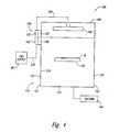
- FIG. 3schematically illustrates an ALD reactor 10 having a reaction chamber 20 coupled to a gas supply 30 and a vacuum 40 .
- the reactor 10also includes a lid 80 coupled to the reaction chamber 20 , a heater 50 that supports the workpiece W, and a gas dispenser 60 in the reaction chamber 20 .
- the gas dispenser 60includes a plenum 62 operatively coupled to the gas supply 30 and a distributor plate 70 having a plurality of holes 72 .
- the heater 50heats the workpiece W to a desired temperature
- the gas supply 30selectively injects the first precursor A x , the purge gas, and the second precursor B y as shown above in FIG. 2 .
- the vacuum 40maintains a negative pressure in the chamber to draw the gases from the gas dispenser 60 across the workpiece W and then through an outlet of the reaction chamber 20 .
- ALD processingtypically takes about eight to eleven seconds to perform each A x -purge-B y -purge cycle. This results in a total process time of approximately eight to eleven minutes to form a single thin layer of only 60 ⁇ .
- CVD techniquesonly require about one minute to form a 60 ⁇ thick layer.
- the low throughput of existing ALD techniqueslimits the utility of the technology in its current state because ALD may be a bottleneck in the overall manufacturing process. Thus, it would be useful to increase the throughput of ALD techniques so they could be used in a wider range of applications.
- VCR connectionstypically develop leaks and need to be replaced after only a few cycles of being disconnected and reconnected.
- Replacing the VCR connectionsrequires substantial downtime because it usually involves cutting the gas lines and welding new VCR connections onto the lines. This causes a significant reduction in throughput, and the new welds may fail or leak. Therefore, there is a significant need to reduce the downtime for servicing components in CVD and ALD chambers.
- a reactor for depositing material onto a micro-device workpieceincludes a reaction chamber, a lid attachable to the reaction chamber, and a connector.
- the connectorhas a first portion coupled to the lid, a second portion coupled to the reaction chamber, a gas passageway extending through the first portion and the second portion, and a seal.
- the sealsurrounds the gas passageway between the first portion and the second portion to prevent gas from leaking from the gas passageway.
- the first portionis detachably coupled to the second portion.
- the connectoralso includes a second gas passageway extending through the first and second portions and a second seal surrounding the second gas passageway.
- the first and second portionscan be coupled to exterior or interior walls of the lid and reaction chamber, respectively.
- the first and second portionscan be mounted directly to the lid and the reaction chamber, respectively.
- the connectorcan further include a temperature control element proximate to the gas passageway to regulate the temperature of the gas.
- the temperature control elementcan be any device that heats and/or cools the gas, such as an electric heater, a gas heater, or a heat exchanger.
- the first portion and/or the second portioncan include a low pressure recess proximate to the gas passageway.
- the first portion and/or the second portioncan also include a leakage channel coupled to the low pressure recess to remove from the connector gas that leaks from the gas passageway into the low pressure recess.
- a method for providing gas to the reactorincludes flowing a gas through a first gas passageway section in the first block coupled to the reaction chamber and flowing the gas through a second gas passageway section in the second block coupled to the lid.
- the first gas passageway sectionis sealably coupled to the second gas passageway section, and the first block is detachably coupled to the second block.
- the methodcan include heating the gas to a desired temperature in the first and/or second gas passageway section.
- FIGS. 1A and 1Bare schematic cross-sectional views of stages in ALD processing in accordance with the prior art.
- FIG. 2is a graph illustrating a cycle for forming a layer using ALD techniques in accordance with the prior art.
- FIG. 3is a schematic representation of a system including a reactor for depositing a material onto a microelectronic workpiece in accordance with the prior art.
- FIG. 4is a schematic side view of a system including a reactor for depositing material onto a micro-device workpiece in accordance with one embodiment of the invention.
- FIG. 5is an isometric view of the connector shown in FIG. 4 with the first portion spaced apart from the second portion.
- FIG. 6is an isometric view of a connector having first portions spaced apart from second portions in accordance with another embodiment of the invention.
- micro-device workpieceis used throughout to include substrates upon which and/or in which microelectronic devices, micromechanical devices, data storage elements, read/write components, and other features are fabricated.
- micro-device workpiecescan be semiconductor wafers such as silicon or gallium arsenide wafers, glass substrates, insulative substrates, and many other types of materials.
- gasis used throughout to include any form of matter that has no fixed shape and will conform in volume to the space available, which specifically includes vapors (i.e., a gas having a temperature less than the critical temperature so that it may be liquefied or solidified by compression at a constant temperature).
- vaporsi.e., a gas having a temperature less than the critical temperature so that it may be liquefied or solidified by compression at a constant temperature.
- FIG. 4is a schematic side view of a system 100 for depositing material onto a micro-device workpiece W in accordance with one embodiment of the invention.
- the system 100includes a reactor 110 having a reaction chamber 120 and a lid 180 coupled to the reaction chamber 120 .
- the reaction chamber 120can include a workpiece holder 150 that supports the workpiece W and a gas dispenser 160 coupled to a gas supply 30 .
- the workpiece holder 150can be a heater or heat sink that holds the workpiece W at a desired temperature.
- the gas dispenser 160is positioned over the workpiece holder 150 to deliver the gas(es) to the workpiece W.
- the lid 180carries the gas dispenser 160 .
- the reaction chamber 120can be coupled to a vacuum 140 to draw gases from the gas dispenser 160 across the workpiece W and then out of the reaction chamber 120 .
- the reactor 110further includes a connector 130 having a first portion 132 coupled to the lid 180 and a second portion 142 coupled to the reaction chamber 120 .
- the first portion 132is attached to a spacer 127 which is mounted to the lid 180
- the second portion 142is attached to a spacer 129 which is mounted to the reaction chamber 120 .
- the first portion 132 and the second portion 142can be mounted directly to the lid 180 and the reaction chamber 120 , respectively.
- the connector 130is coupled to an external wall 125 on a first side 121 of the reaction chamber 120 and the lid 180 .
- the connector 130can alternatively be coupled to other portions of the reaction chamber 120 and the lid 180 , such as a second side 122 or a third side 123 , in other embodiments. Furthermore, in still other embodiments, the connector 130 can be coupled to internal walls 124 of the reaction chamber 120 and the lid 180 .
- the first portion 132 of the connector 130is coupled to the gas dispenser 160 by a first gas conduit 126 .
- the second portion 142is coupled to the gas supply 30 by a second gas conduit 128 .
- the first and second portions 132 and 142include at least one internal gas passageway that will be discussed in detail below.
- the connector 130thereby connects the first gas conduit 126 to the second gas conduit 128 so that gas can flow from the gas supply 30 to the gas dispenser 160 .
- FIG. 5is an isometric view of one embodiment of the connector 130 shown in FIG. 4 with the first portion 132 disconnected from the second portion 142 .
- the first portion 132is a first block that includes a plurality of first gas passageway sections (identified individually as 131 a - c ) extending from a first side 133 to a second side 134 .
- Each first section 131 a - cis coupled to a corresponding first gas conduit (identified individually as 126 a - c ) proximate to the second side 134 .
- the second portion 142is a second block that includes a plurality of second gas passageway sections (identified individually as 141 a - c ) extending from a first side 143 to a second side 144 .
- Each second section 141 a - cis coupled to a corresponding second gas conduit (identified individually as 128 a - c ) proximate to the second side 144 .
- each first section 131 a - c in the first portion 132is axially aligned with a corresponding second section 141 a - c in the second portion 142 to define individual gas passageways.
- first section 131 ais aligned with second section 141 a so that gas can flow from the second gas conduit 128 a , through the second and first sections 141 a and 131 a , and then through the first gas conduit 126 a .
- the gas passageway sections 131 a and 141 aaccordingly define a first passageway through the connector 130 for transporting a first gas.
- the gas passageway sections 131 b and 141 bdefine a second passageway through the connector 130 for transporting a second gas
- the gas passageway sections 131 c and 141 cdefine a third passageway through the connector 130 for transporting a third gas.
- Each passagewaycontains a separate, discrete flow of a gas to prevent the individual gas flows from mixing with each other in the conduits 126 and 128 .
- the connector 130can have a different number of gas passageways.
- the connector 130can be made of a noncorrosive material, such as stainless steel or invar, that is compatible with caustic gases.
- the connector 130can also include seals 146 between inlets 135 of the first gas passageway sections 131 a - c and inlets 145 of the second gas passageway sections 141 a - c .
- the seals 146prevent gases from leaking while flowing between the first portion 132 and the second portion 142 .
- the first side 143 of the second portion 142 and/or the first side 133 of the first portion 132can include grooves circumscribing the inlets 135 and 145 that are sized to seat the seals 146 .
- the seals 146can be O-rings, gaskets or metal rings.
- the seals 146can be a raised ridge surrounding each of the inlets 135 and a corresponding flat surface or depression around each of the inlets 145 , such as a knife edge seal. It will be appreciated that the ridges can surround the inlets 145 and the receiving surfaces can surround the inlets 135 .
- the seals 146can be a combination of moveable seals (e.g., O-rings) and fixed seals (e.g., knife-edge seals) around each inlet pair.
- the second portion 142can also include a low pressure recess 147 in the first side 143 and leakage channels 151 coupled to the low pressure recess 147 to remove leaked or spilled gas from inside the connector 130 .
- the seals 146 and the inlets 145can be located within the low pressure recess 147 .
- Inlets 149connect the leakage channels 151 to the low pressure recess 147 .
- a vacuum(not shown) can be coupled to the leakage channels 151 to create the low pressure in the low pressure recess 147 and to remove the leaked gas from the low pressure recess 147 .
- the low pressure in the low pressure recess 147prevents leaked gas from contaminating the discrete gas flows in the passageway sections 131 a - c and 141 a - c .
- the connector 130 of the illustrated embodimentfurther includes a seal 148 circumscribing the low pressure recess 147 to prevent leaked gas from passing out of the low pressure recess 147 .
- the connector 130may not include the seal 148 circumscribing the low pressure recess 147 .
- the connector 130may not include the low pressure recess 147 , or may have a low pressure recess with a different configuration, such as that described below with reference to FIG. 6 .
- the first portion 132may have the low pressure recess 147 .
- the connector 130optionally include temperature control elements 154 positioned proximate to the gas passageway sections 131 a - c and 141 a - c .
- the temperature control elements 154heat and/or cool each gas passageway section 131 a - c and 141 a - c individually to maintain an optimal temperature for each specific gas.
- the temperature control elements 154can heat the gas passageway sections 131 a - c and 141 a - c collectively as a group in other embodiments.
- the temperature control elements 154can be electric heaters, gas heaters, heat exchangers, or other devices to heat and/or cool the gas passageway sections 131 a - c and 141 a - c .
- Each temperature control element 154can be a single unit with discrete portions or several units to control the temperature of each gas passageway section 131 a - c and 141 a - c individually.
- the first portion 132 and/or the second portion 142may not include the temperature control element 154 .
- the first portion 132 and the second portion 142 of the connector 130are detachably coupled together so that gases flow from the gas supply 30 ( FIG. 4 ) through the connector 130 to the gas distributor 160 ( FIG. 4 ). If gas leaks while flowing from the second gas passageway sections 141 a - c to the first gas passageway sections 131 a - c , the low pressure recess 147 entraps the leaked gas for removal via the leakage channels 151 .
- one advantage of the illustrated embodimentis that the lid 180 can be removed from the reaction chamber 120 without disconnecting a VCR connection in the gas conduits 126 and 128 .
- the connector 130eliminates the need for VCR connections that are subject to premature failure and instead provides a system with a more robust and/or replaceable seal.
- Several embodiments of the connectorare expected to reduce the need to replace worn or faulty VCR connections. Accordingly, the illustrated embodiment reduces the downtime required to service components in the reaction chamber 120 , such as replacing faulty VCR connections.
- Another advantage of the illustrated embodimentis the ability to control the temperature of each gas just before introducing the gases to the gas distributor 160 ( FIG. 4 ).
- Several embodiments of the connector 130 with temperature control elements 154bring the individual gas flows to the desired temperatures in the gas conduits 126 and 128 . Maintaining the desired temperature of each gas reduces condensation and degradation of the gas in the gas conduits 126 and 128 .
- the temperature control elements 154can superheat the gases just before they enter the reaction chamber 120 to produce smaller droplets. Smaller droplets are advantageous because they form a more uniform surface on the workpiece W.
- FIG. 6is an isometric view of a connector 230 having first portions (identified individually as 232 a - c ) spaced apart from second portions (identified individually as 242 a - c ) in accordance with another embodiment of the invention.
- the first portions 232 a - care spaced apart from each other by a gap G, and each first portion 232 a - c is coupled to the lid 180 ( FIG. 4 ).
- the second portions 242 a - care spaced apart from each other by the gap G, and each second portion 242 a - c is coupled to the reaction chamber 120 ( FIG. 4 ).
- the second portion 242 aincludes a low pressure recess 247 , a leakage channel 251 , and a temperature control element 254 , all of which are similar to those discussed above with reference to FIG. 5 .
- the second portion 242 amay not include all of these elements.
- some or all of the first and second portions 232 a - c and 242 a - cmay also include low pressure recesses, leakage conduits, and/or temperature control elements.
- One advantage of the embodiment illustrated in FIG. 6is that the gap G between each first portion 232 a - c and between each second portion 242 a - c helps thermally insulate each portion from the adjacent portion. Furthermore, the gap G permits a cooling and/or heating gas, such as air, to move between the portions 232 a - c and 242 a - c to cool and/or heat each portion individually.
Landscapes
- Chemical & Material Sciences (AREA)
- General Chemical & Material Sciences (AREA)
- Chemical Kinetics & Catalysis (AREA)
- Engineering & Computer Science (AREA)
- Materials Engineering (AREA)
- Mechanical Engineering (AREA)
- Metallurgy (AREA)
- Organic Chemistry (AREA)
- Chemical Vapour Deposition (AREA)
Abstract
Description
- The present invention is related to reactors with isolated gas connectors and methods for depositing materials in thin film deposition processes used in the manufacturing of micro-devices.
- Thin film deposition techniques are widely used in the manufacturing of micro-devices to form a coating on a workpiece that closely conforms to the surface topography. The size of the individual components in the devices is constantly decreasing, and the number of layers in the devices is increasing. As a result, the density of components and the aspect ratios of depressions (e.g., the ratio of the depth to the size of the opening) are increasing. The size of workpieces is also increasing to provide more real estate for forming more dies (i.e., chips) on a single workpiece. Many fabricators, for example, are transitioning from 200 mm to 300 mm workpieces, and even larger workpieces will likely be used in the future. Thin film deposition techniques accordingly strive to produce highly uniform conformal layers that cover the sidewalls, bottoms, and corners in deep depressions that have very small openings.
- One widely used thin film deposition technique is Chemical Vapor Deposition (CVD). In a CVD system, one or more precursors that are capable of reacting to form a solid thin film are mixed in a gas or vapor state, and then the precursor mixture is presented to the surface of the workpiece. The surface of the workpiece catalyzes the reaction between the precursors to form a thin solid film at the workpiece surface. A common way to catalyze the reaction at the surface of the workpiece is to heat the workpiece to a temperature that causes the reaction.
- Although CVD techniques are useful in many applications, they also have several drawbacks. For example, if the precursors are not highly reactive, then a high workpiece temperature is needed to achieve a reasonable deposition rate. Such high temperatures are not typically desirable because heating the workpiece can be detrimental to the structures and other materials already formed on the workpiece. Implanted or doped materials, for example, can migrate within the silicon substrate at higher temperatures. On the other hand, if more reactive precursors are used so that the workpiece temperature can be lower, then reactions may occur prematurely in the gas phase before reaching the substrate. This is undesirable because the film quality and uniformity may suffer, and also because it limits the types of precursors that can be used.
- Atomic Layer Deposition (ALD) is another thin film deposition technique.
FIGS. 1A and 1B schematically illustrate the basic operation of ALD processes. Referring toFIG. 1A , a layer of gas molecules Axcoats the surface of a workpiece W. The layer of Axmolecules is formed by exposing the workpiece W to a precursor gas containing Axmolecules, and then purging the chamber with a purge gas to remove excess Axmolecules. This process can form a monolayer of Axmolecules on the surface of the workpiece W because the Axmolecules at the surface are held in place during the purge cycle by physical adsorption forces at moderate temperatures or chemisorption forces at higher temperatures. The layer of Axmolecules is then exposed to another precursor gas containing Bymolecules. The Axmolecules react with the Bymolecules to form an extremely thin layer of solid material on the workpiece W. The chamber is then purged again with a purge gas to remove excess Bymolecules. FIG. 2 illustrates the stages of one cycle for forming a thin solid layer using ALD techniques. A typical cycle includes (a) exposing the workpiece to the first precursor Ax, (b) purging excess Axmolecules, (c) exposing the workpiece to the second precursor By, and then (d) purging excess Bymolecules. In actual processing, several cycles are repeated to build a thin film on a workpiece having the desired thickness. For example, each cycle may form a layer having a thickness of approximately 0.5-1.0 Å, and thus it takes approximately 60-120 cycles to form a solid layer having a thickness of approximately 60 Å.FIG. 3 schematically illustrates anALD reactor 10 having areaction chamber 20 coupled to agas supply 30 and avacuum 40. Thereactor 10 also includes alid 80 coupled to thereaction chamber 20, aheater 50 that supports the workpiece W, and agas dispenser 60 in thereaction chamber 20. Thegas dispenser 60 includes aplenum 62 operatively coupled to thegas supply 30 and adistributor plate 70 having a plurality ofholes 72. In operation, theheater 50 heats the workpiece W to a desired temperature, and the gas supply30 selectively injects the first precursor Ax, the purge gas, and the second precursor Byas shown above inFIG. 2 . Thevacuum 40 maintains a negative pressure in the chamber to draw the gases from thegas dispenser 60 across the workpiece W and then through an outlet of thereaction chamber 20.- One drawback of ALD processing is that it has a relatively low throughput compared to CVD techniques. For example, ALD processing typically takes about eight to eleven seconds to perform each Ax-purge-By-purge cycle. This results in a total process time of approximately eight to eleven minutes to form a single thin layer of only 60 Å. In contrast to ALD processing, CVD techniques only require about one minute to form a 60 Å thick layer. The low throughput of existing ALD techniques limits the utility of the technology in its current state because ALD may be a bottleneck in the overall manufacturing process. Thus, it would be useful to increase the throughput of ALD techniques so they could be used in a wider range of applications.
- Another drawback of both ALD and CVD processing is the difficulty in servicing the components in the
reaction chamber 20 and/or thelid 80. Thelid 80 must be removed from thereaction chamber 20 to clean thegas dispenser 60. In conventional systems, gas lines between thegas supply 30 and thelid 80 are coupled together with VCR connections that can degrade with use. For example, VCR connections typically develop leaks and need to be replaced after only a few cycles of being disconnected and reconnected. Replacing the VCR connections requires substantial downtime because it usually involves cutting the gas lines and welding new VCR connections onto the lines. This causes a significant reduction in throughput, and the new welds may fail or leak. Therefore, there is a significant need to reduce the downtime for servicing components in CVD and ALD chambers. - The present invention is directed toward reactors having isolated gas connectors, systems that include such reactors, and methods for depositing materials onto micro-device workpieces. In one embodiment, a reactor for depositing material onto a micro-device workpiece includes a reaction chamber, a lid attachable to the reaction chamber, and a connector. The connector has a first portion coupled to the lid, a second portion coupled to the reaction chamber, a gas passageway extending through the first portion and the second portion, and a seal. The seal surrounds the gas passageway between the first portion and the second portion to prevent gas from leaking from the gas passageway. The first portion is detachably coupled to the second portion. In one aspect of this embodiment, the connector also includes a second gas passageway extending through the first and second portions and a second seal surrounding the second gas passageway. In another aspect of this embodiment, the first and second portions can be coupled to exterior or interior walls of the lid and reaction chamber, respectively. In yet another aspect of this embodiment, the first and second portions can be mounted directly to the lid and the reaction chamber, respectively.
- In another aspect of this embodiment, the connector can further include a temperature control element proximate to the gas passageway to regulate the temperature of the gas. The temperature control element can be any device that heats and/or cools the gas, such as an electric heater, a gas heater, or a heat exchanger. In still another aspect of this embodiment, the first portion and/or the second portion can include a low pressure recess proximate to the gas passageway. In this embodiment, the first portion and/or the second portion can also include a leakage channel coupled to the low pressure recess to remove from the connector gas that leaks from the gas passageway into the low pressure recess.
- The connectors can be used to perform several methods for depositing materials onto micro-device workpieces. In one embodiment, a method for providing gas to the reactor includes flowing a gas through a first gas passageway section in the first block coupled to the reaction chamber and flowing the gas through a second gas passageway section in the second block coupled to the lid. The first gas passageway section is sealably coupled to the second gas passageway section, and the first block is detachably coupled to the second block. In a further aspect of this embodiment, the method can include heating the gas to a desired temperature in the first and/or second gas passageway section.
FIGS. 1A and 1B are schematic cross-sectional views of stages in ALD processing in accordance with the prior art.FIG. 2 is a graph illustrating a cycle for forming a layer using ALD techniques in accordance with the prior art.FIG. 3 is a schematic representation of a system including a reactor for depositing a material onto a microelectronic workpiece in accordance with the prior art.FIG. 4 is a schematic side view of a system including a reactor for depositing material onto a micro-device workpiece in accordance with one embodiment of the invention.FIG. 5 is an isometric view of the connector shown inFIG. 4 with the first portion spaced apart from the second portion.FIG. 6 is an isometric view of a connector having first portions spaced apart from second portions in accordance with another embodiment of the invention.- The following disclosure describes several embodiments of reactors having isolated gas connectors, systems including such reactors, and methods for depositing materials onto micro-device workpieces. Many specific details of the invention are described below with reference to reactors for depositing materials onto micro-device workpieces. The term “micro-device workpiece” is used throughout to include substrates upon which and/or in which microelectronic devices, micromechanical devices, data storage elements, read/write components, and other features are fabricated. For example, micro-device workpieces can be semiconductor wafers such as silicon or gallium arsenide wafers, glass substrates, insulative substrates, and many other types of materials. The term “gas” is used throughout to include any form of matter that has no fixed shape and will conform in volume to the space available, which specifically includes vapors (i.e., a gas having a temperature less than the critical temperature so that it may be liquefied or solidified by compression at a constant temperature). Several embodiments in accordance with the invention are set forth in
FIGS. 4-6 and the following text to provide a thorough understanding of particular embodiments of the invention. A person skilled in the art will understand, however, that the invention may have additional embodiments, or that the invention may be practiced without several of the details of the embodiments shown inFIGS. 4-6 . - A. Deposition Systems
FIG. 4 is a schematic side view of asystem 100 for depositing material onto a micro-device workpiece W in accordance with one embodiment of the invention. In this embodiment, thesystem 100 includes areactor 110 having areaction chamber 120 and alid 180 coupled to thereaction chamber 120. Thereaction chamber 120 can include aworkpiece holder 150 that supports the workpiece W and agas dispenser 160 coupled to agas supply 30. Theworkpiece holder 150 can be a heater or heat sink that holds the workpiece W at a desired temperature. Thegas dispenser 160 is positioned over theworkpiece holder 150 to deliver the gas(es) to the workpiece W. In the embodiment shown inFIG. 4 , thelid 180 carries thegas dispenser 160. Thereaction chamber 120 can be coupled to avacuum 140 to draw gases from thegas dispenser 160 across the workpiece W and then out of thereaction chamber 120.- The
reactor 110 further includes aconnector 130 having afirst portion 132 coupled to thelid 180 and asecond portion 142 coupled to thereaction chamber 120. In the illustrated embodiment, thefirst portion 132 is attached to aspacer 127 which is mounted to thelid 180, and thesecond portion 142 is attached to aspacer 129 which is mounted to thereaction chamber 120. In other embodiments, thefirst portion 132 and thesecond portion 142 can be mounted directly to thelid 180 and thereaction chamber 120, respectively. In the illustrated embodiment, theconnector 130 is coupled to anexternal wall 125 on afirst side 121 of thereaction chamber 120 and thelid 180. Theconnector 130 can alternatively be coupled to other portions of thereaction chamber 120 and thelid 180, such as asecond side 122 or athird side 123, in other embodiments. Furthermore, in still other embodiments, theconnector 130 can be coupled tointernal walls 124 of thereaction chamber 120 and thelid 180. - The
first portion 132 of theconnector 130 is coupled to thegas dispenser 160 by afirst gas conduit 126. Thesecond portion 142 is coupled to thegas supply 30 by asecond gas conduit 128. The first andsecond portions connector 130 thereby connects thefirst gas conduit 126 to thesecond gas conduit 128 so that gas can flow from thegas supply 30 to thegas dispenser 160. - B. Connectors
FIG. 5 is an isometric view of one embodiment of theconnector 130 shown inFIG. 4 with thefirst portion 132 disconnected from thesecond portion 142. In this embodiment, thefirst portion 132 is a first block that includes a plurality of first gas passageway sections (identified individually as131a-c) extending from afirst side 133 to asecond side 134. Each first section131a-cis coupled to a corresponding first gas conduit (identified individually as126a-c) proximate to thesecond side 134. Similarly, thesecond portion 142 is a second block that includes a plurality of second gas passageway sections (identified individually as141a-c) extending from afirst side 143 to asecond side 144. Each second section141a-cis coupled to a corresponding second gas conduit (identified individually as128a-c) proximate to thesecond side 144. Furthermore, each first section131a-cin thefirst portion 132 is axially aligned with a corresponding second section141a-cin thesecond portion 142 to define individual gas passageways. For example,first section 131ais aligned with second section141aso that gas can flow from thesecond gas conduit 128a, through the second andfirst sections 141aand131a, and then through thefirst gas conduit 126a. Thegas passageway sections 131aand141aaccordingly define a first passageway through theconnector 130 for transporting a first gas. Thegas passageway sections connector 130 for transporting a second gas, and thegas passageway sections connector 130 for transporting a third gas. Each passageway contains a separate, discrete flow of a gas to prevent the individual gas flows from mixing with each other in theconduits connector 130 can have a different number of gas passageways. In a further aspect of the illustrated embodiment, theconnector 130 can be made of a noncorrosive material, such as stainless steel or invar, that is compatible with caustic gases.- The
connector 130 can also includeseals 146 betweeninlets 135 of the first gas passageway sections131a-candinlets 145 of the second gas passageway sections141a-c. Theseals 146 prevent gases from leaking while flowing between thefirst portion 132 and thesecond portion 142. In other embodiments, thefirst side 143 of thesecond portion 142 and/or thefirst side 133 of thefirst portion 132 can include grooves circumscribing theinlets seals 146. Theseals 146 can be O-rings, gaskets or metal rings. Alternatively, theseals 146 can be a raised ridge surrounding each of theinlets 135 and a corresponding flat surface or depression around each of theinlets 145, such as a knife edge seal. It will be appreciated that the ridges can surround theinlets 145 and the receiving surfaces can surround theinlets 135. Moreover, theseals 146 can be a combination of moveable seals (e.g., O-rings) and fixed seals (e.g., knife-edge seals) around each inlet pair. - The
second portion 142 can also include alow pressure recess 147 in thefirst side 143 andleakage channels 151 coupled to thelow pressure recess 147 to remove leaked or spilled gas from inside theconnector 130. Theseals 146 and theinlets 145 can be located within thelow pressure recess 147.Inlets 149 connect theleakage channels 151 to thelow pressure recess 147. In one embodiment, a vacuum (not shown) can be coupled to theleakage channels 151 to create the low pressure in thelow pressure recess 147 and to remove the leaked gas from thelow pressure recess 147. The low pressure in thelow pressure recess 147 prevents leaked gas from contaminating the discrete gas flows in the passageway sections131a-cand141a-c. Theconnector 130 of the illustrated embodiment further includes aseal 148 circumscribing thelow pressure recess 147 to prevent leaked gas from passing out of thelow pressure recess 147. In other embodiments, theconnector 130 may not include theseal 148 circumscribing thelow pressure recess 147. In additional embodiments, theconnector 130 may not include thelow pressure recess 147, or may have a low pressure recess with a different configuration, such as that described below with reference toFIG. 6 . In still other embodiments, thefirst portion 132 may have thelow pressure recess 147. - Several embodiments of the
connector 130 optionally includetemperature control elements 154 positioned proximate to the gas passageway sections131a-cand141a-c. In many embodiments, thetemperature control elements 154 heat and/or cool each gas passageway section131a-cand141a-cindividually to maintain an optimal temperature for each specific gas. Thetemperature control elements 154, however, can heat the gas passageway sections131a-cand141a-ccollectively as a group in other embodiments. Thetemperature control elements 154 can be electric heaters, gas heaters, heat exchangers, or other devices to heat and/or cool the gas passageway sections131a-cand141a-c. Eachtemperature control element 154 can be a single unit with discrete portions or several units to control the temperature of each gas passageway section131a-cand141a-cindividually. In other embodiments, thefirst portion 132 and/or thesecond portion 142 may not include thetemperature control element 154. - In operation, the
first portion 132 and thesecond portion 142 of theconnector 130 are detachably coupled together so that gases flow from the gas supply30 (FIG. 4 ) through theconnector 130 to the gas distributor160 (FIG. 4 ). If gas leaks while flowing from the second gas passageway sections141a-cto the first gas passageway sections131a-c, thelow pressure recess 147 entraps the leaked gas for removal via theleakage channels 151. - Referring to
FIG. 4 , one advantage of the illustrated embodiment is that thelid 180 can be removed from thereaction chamber 120 without disconnecting a VCR connection in thegas conduits connector 130 eliminates the need for VCR connections that are subject to premature failure and instead provides a system with a more robust and/or replaceable seal. Several embodiments of the connector are expected to reduce the need to replace worn or faulty VCR connections. Accordingly, the illustrated embodiment reduces the downtime required to service components in thereaction chamber 120, such as replacing faulty VCR connections. - Another advantage of the illustrated embodiment is the ability to control the temperature of each gas just before introducing the gases to the gas distributor160 (
FIG. 4 ). Several embodiments of theconnector 130 withtemperature control elements 154 bring the individual gas flows to the desired temperatures in thegas conduits gas conduits temperature control elements 154 can superheat the gases just before they enter thereaction chamber 120 to produce smaller droplets. Smaller droplets are advantageous because they form a more uniform surface on the workpiece W. FIG. 6 is an isometric view of aconnector 230 having first portions (identified individually as232a-c) spaced apart from second portions (identified individually as242a-c) in accordance with another embodiment of the invention. The first portions232a-care spaced apart from each other by a gap G, and each first portion232a-cis coupled to the lid180 (FIG. 4 ). Similarly, the second portions242a-care spaced apart from each other by the gap G, and each second portion242a-cis coupled to the reaction chamber120 (FIG. 4 ). In the illustrated embodiment, thesecond portion 242aincludes alow pressure recess 247, aleakage channel 251, and atemperature control element 254, all of which are similar to those discussed above with reference toFIG. 5 . In additional embodiments, thesecond portion 242amay not include all of these elements. In other embodiments, some or all of the first and second portions232a-cand242a-cmay also include low pressure recesses, leakage conduits, and/or temperature control elements. One advantage of the embodiment illustrated inFIG. 6 is that the gap G between each first portion232a-cand between each second portion242a-chelps thermally insulate each portion from the adjacent portion. Furthermore, the gap G permits a cooling and/or heating gas, such as air, to move between the portions232a-cand242a-cto cool and/or heat each portion individually.- From the foregoing, it will be appreciated that specific embodiments of the invention have been described herein for purposes of illustration, but that various modifications may be made without deviating from the spirit and scope of the invention. Accordingly, the invention is not limited except as by the appended claims.
Claims (16)
Priority Applications (1)
| Application Number | Priority Date | Filing Date | Title |
|---|---|---|---|
| US10/922,039US7588804B2 (en) | 2002-08-15 | 2004-08-19 | Reactors with isolated gas connectors and methods for depositing materials onto micro-device workpieces |
Applications Claiming Priority (2)
| Application Number | Priority Date | Filing Date | Title |
|---|---|---|---|
| US10/222,289US6955725B2 (en) | 2002-08-15 | 2002-08-15 | Reactors with isolated gas connectors and methods for depositing materials onto micro-device workpieces |
| US10/922,039US7588804B2 (en) | 2002-08-15 | 2004-08-19 | Reactors with isolated gas connectors and methods for depositing materials onto micro-device workpieces |
Related Parent Applications (1)
| Application Number | Title | Priority Date | Filing Date |
|---|---|---|---|
| US10/222,289DivisionUS6955725B2 (en) | 2002-08-15 | 2002-08-15 | Reactors with isolated gas connectors and methods for depositing materials onto micro-device workpieces |
Publications (2)
| Publication Number | Publication Date |
|---|---|
| US20050016984A1true US20050016984A1 (en) | 2005-01-27 |
| US7588804B2 US7588804B2 (en) | 2009-09-15 |
Family
ID=32174451
Family Applications (2)
| Application Number | Title | Priority Date | Filing Date |
|---|---|---|---|
| US10/222,289Expired - Fee RelatedUS6955725B2 (en) | 2002-08-15 | 2002-08-15 | Reactors with isolated gas connectors and methods for depositing materials onto micro-device workpieces |
| US10/922,039Expired - Fee RelatedUS7588804B2 (en) | 2002-08-15 | 2004-08-19 | Reactors with isolated gas connectors and methods for depositing materials onto micro-device workpieces |
Family Applications Before (1)
| Application Number | Title | Priority Date | Filing Date |
|---|---|---|---|
| US10/222,289Expired - Fee RelatedUS6955725B2 (en) | 2002-08-15 | 2002-08-15 | Reactors with isolated gas connectors and methods for depositing materials onto micro-device workpieces |
Country Status (1)
| Country | Link |
|---|---|
| US (2) | US6955725B2 (en) |
Cited By (21)
| Publication number | Priority date | Publication date | Assignee | Title |
|---|---|---|---|---|
| US20040049908A1 (en)* | 2002-01-15 | 2004-03-18 | Quallion Llc | Electric storage battery construction and method of manufacture |
| US20040226507A1 (en)* | 2003-04-24 | 2004-11-18 | Carpenter Craig M. | Methods for controlling mass flow rates and pressures in passageways coupled to reaction chambers and systems for depositing material onto microfeature workpieces in reaction chambers |
| US20050022739A1 (en)* | 2002-07-08 | 2005-02-03 | Carpenter Craig M. | Apparatus and method for depositing materials onto microelectronic workpieces |
| US20050039680A1 (en)* | 2003-08-21 | 2005-02-24 | Beaman Kevin L. | Methods and apparatus for processing microfeature workpieces; methods for conditioning ALD reaction chambers |
| US20050081786A1 (en)* | 2003-10-15 | 2005-04-21 | Kubista David J. | Systems for depositing material onto workpieces in reaction chambers and methods for removing byproducts from reaction chambers |
| US20050087130A1 (en)* | 2003-10-09 | 2005-04-28 | Derderian Garo J. | Apparatus and methods for plasma vapor deposition processes |
| US20050087302A1 (en)* | 2003-10-10 | 2005-04-28 | Mardian Allen P. | Apparatus and methods for manufacturing microfeatures on workpieces using plasma vapor processes |
| US20050126489A1 (en)* | 2003-12-10 | 2005-06-16 | Beaman Kevin L. | Methods and systems for controlling temperature during microfeature workpiece processing, e.g., CVD deposition |
| US20050164466A1 (en)* | 2004-01-28 | 2005-07-28 | Zheng Lingyi A. | Methods for forming small-scale capacitor structures |
| US20050249873A1 (en)* | 2004-05-05 | 2005-11-10 | Demetrius Sarigiannis | Apparatuses and methods for producing chemically reactive vapors used in manufacturing microelectronic devices |
| US20050249887A1 (en)* | 2004-05-06 | 2005-11-10 | Dando Ross S | Methods for depositing material onto microfeature workpieces in reaction chambers and systems for depositing materials onto microfeature workpieces |
| US20050268856A1 (en)* | 2004-06-02 | 2005-12-08 | Miller Matthew W | Reactors, systems and methods for depositing thin films onto microfeature workpieces |
| US20060115957A1 (en)* | 2003-09-17 | 2006-06-01 | Cem Basceri | Microfeature workpiece processing apparatus and methods for controlling deposition of materials on microfeature workpieces |
| US20060165873A1 (en)* | 2005-01-25 | 2006-07-27 | Micron Technology, Inc. | Plasma detection and associated systems and methods for controlling microfeature workpiece deposition processes |
| US20060198955A1 (en)* | 2003-08-21 | 2006-09-07 | Micron Technology, Inc. | Microfeature workpiece processing apparatus and methods for batch deposition of materials on microfeature workpieces |
| US20060205187A1 (en)* | 2003-08-28 | 2006-09-14 | Micron Technology, Inc. | Methods and apparatus for processing microfeature workpieces, e.g., for depositing materials on microfeature workpieces |
| US20060237138A1 (en)* | 2005-04-26 | 2006-10-26 | Micron Technology, Inc. | Apparatuses and methods for supporting microelectronic devices during plasma-based fabrication processes |
| US7282239B2 (en) | 2003-09-18 | 2007-10-16 | Micron Technology, Inc. | Systems and methods for depositing material onto microfeature workpieces in reaction chambers |
| US7481887B2 (en) | 2002-05-24 | 2009-01-27 | Micron Technology, Inc. | Apparatus for controlling gas pulsing in processes for depositing materials onto micro-device workpieces |
| US7584942B2 (en) | 2004-03-31 | 2009-09-08 | Micron Technology, Inc. | Ampoules for producing a reaction gas and systems for depositing materials onto microfeature workpieces in reaction chambers |
| WO2012166439A1 (en)* | 2011-05-27 | 2012-12-06 | Dsa Detection Llc | Multi-dopant permeation tube |
Families Citing this family (9)
| Publication number | Priority date | Publication date | Assignee | Title |
|---|---|---|---|---|
| TWI224815B (en)* | 2001-08-01 | 2004-12-01 | Tokyo Electron Ltd | Gas processing apparatus and gas processing method |
| US6955725B2 (en) | 2002-08-15 | 2005-10-18 | Micron Technology, Inc. | Reactors with isolated gas connectors and methods for depositing materials onto micro-device workpieces |
| JP4636807B2 (en)* | 2004-03-18 | 2011-02-23 | キヤノン株式会社 | Substrate holding device and exposure apparatus using the same |
| US8211235B2 (en)* | 2005-03-04 | 2012-07-03 | Picosun Oy | Apparatuses and methods for deposition of material on surfaces |
| KR102385794B1 (en)* | 2015-04-07 | 2022-04-11 | 셀 아이디 피티이 엘티디 | A dc heater |
| US11384432B2 (en)* | 2015-04-22 | 2022-07-12 | Applied Materials, Inc. | Atomic layer deposition chamber with funnel-shaped gas dispersion channel and gas distribution plate |
| US10400332B2 (en)* | 2017-03-14 | 2019-09-03 | Eastman Kodak Company | Deposition system with interlocking deposition heads |
| US10501848B2 (en)* | 2017-03-14 | 2019-12-10 | Eastman Kodak Company | Deposition system with modular deposition heads |
| US10889894B2 (en)* | 2018-08-06 | 2021-01-12 | Applied Materials, Inc. | Faceplate with embedded heater |
Citations (98)
| Publication number | Priority date | Publication date | Assignee | Title |
|---|---|---|---|---|
| US5091207A (en)* | 1989-07-20 | 1992-02-25 | Fujitsu Limited | Process and apparatus for chemical vapor deposition |
| US5090985A (en)* | 1989-10-17 | 1992-02-25 | Libbey-Owens-Ford Co. | Method for preparing vaporized reactants for chemical vapor deposition |
| US5178683A (en)* | 1990-03-30 | 1993-01-12 | New Japan Radio Co., Ltd. | Microwave plasma cvd apparatus |
| US5286296A (en)* | 1991-01-10 | 1994-02-15 | Sony Corporation | Multi-chamber wafer process equipment having plural, physically communicating transfer means |
| US5377429A (en)* | 1993-04-19 | 1995-01-03 | Micron Semiconductor, Inc. | Method and appartus for subliming precursors |
| US5378502A (en)* | 1992-09-09 | 1995-01-03 | U.S. Philips Corporation | Method of chemically modifying a surface in accordance with a pattern |
| US5380396A (en)* | 1991-05-30 | 1995-01-10 | Hitachi, Ltd. | Valve and semiconductor fabricating equipment using the same |
| US5480818A (en)* | 1992-02-10 | 1996-01-02 | Fujitsu Limited | Method for forming a film and method for manufacturing a thin film transistor |
| US5496410A (en)* | 1992-03-10 | 1996-03-05 | Hitachi, Ltd. | Plasma processing apparatus and method of processing substrates by using same apparatus |
| US5498292A (en)* | 1994-06-16 | 1996-03-12 | Kishimoto Sangyo Co., Ltd. | Heating device used for a gas phase growing mechanism or heat treatment mechanism |
| US5500256A (en)* | 1994-08-16 | 1996-03-19 | Fujitsu Limited | Dry process apparatus using plural kinds of gas |
| US5592581A (en)* | 1993-07-19 | 1997-01-07 | Tokyo Electron Kabushiki Kaisha | Heat treatment apparatus |
| US5595606A (en)* | 1995-04-20 | 1997-01-21 | Tokyo Electron Limited | Shower head and film forming apparatus using the same |
| US5599513A (en)* | 1989-11-13 | 1997-02-04 | Showa Denko K.K. | Gas distribution plate for use with fluidized-bed gas-phase polymerizer |
| US5609798A (en)* | 1995-06-07 | 1997-03-11 | Msp Corporation | High output PSL aerosol generator |
| US5716796A (en)* | 1990-01-23 | 1998-02-10 | Medical Devices Corporation | Optical blood hemostatic analysis apparatus and method |
| US5729896A (en)* | 1996-10-31 | 1998-03-24 | International Business Machines Corporation | Method for attaching a flip chip on flexible circuit carrier using chip with metallic cap on solder |
| US5733375A (en)* | 1995-01-06 | 1998-03-31 | Tokyo Electron Limited | Apparatus for supplying a treatment material |
| US5865887A (en)* | 1996-09-13 | 1999-02-02 | Seh America, Inc. | Method for improving mechanical strength of the neck section of czochralski silicon crystal |
| US5866986A (en)* | 1996-08-05 | 1999-02-02 | Integrated Electronic Innovations, Inc. | Microwave gas phase plasma source |
| US5865417A (en)* | 1996-09-27 | 1999-02-02 | Redwood Microsystems, Inc. | Integrated electrically operable normally closed valve |
| US5868159A (en)* | 1996-07-12 | 1999-02-09 | Mks Instruments, Inc. | Pressure-based mass flow controller |
| US5879516A (en)* | 1996-02-29 | 1999-03-09 | Kasman; David H. | Kugelrohr or distillation apparatus |
| US5879459A (en)* | 1997-08-29 | 1999-03-09 | Genus, Inc. | Vertically-stacked process reactor and cluster tool system for atomic layer deposition |
| US5885425A (en)* | 1995-06-06 | 1999-03-23 | International Business Machines Corporation | Method for selective material deposition on one side of raised or recessed features |
| US6016611A (en)* | 1998-07-13 | 2000-01-25 | Applied Komatsu Technology, Inc. | Gas flow control in a substrate processing system |
| US6022483A (en)* | 1998-03-10 | 2000-02-08 | Intergrated Systems, Inc. | System and method for controlling pressure |
| US6025110A (en)* | 1997-09-18 | 2000-02-15 | Nowak; Michael T. | Method and apparatus for generating three-dimensional objects using ablation transfer |
| US6032923A (en)* | 1998-01-08 | 2000-03-07 | Xerox Corporation | Fluid valves having cantilevered blocking films |
| US6039557A (en)* | 1989-12-22 | 2000-03-21 | Imarx Pharmaceutical Corp. | Apparatus for making gas-filled vesicles of optimal size |
| US6042652A (en)* | 1999-05-01 | 2000-03-28 | P.K. Ltd | Atomic layer deposition apparatus for depositing atomic layer on multiple substrates |
| US6174809B1 (en)* | 1997-12-31 | 2001-01-16 | Samsung Electronics, Co., Ltd. | Method for forming metal layer using atomic layer deposition |
| US6173673B1 (en)* | 1999-03-31 | 2001-01-16 | Tokyo Electron Limited | Method and apparatus for insulating a high power RF electrode through which plasma discharge gases are injected into a processing chamber |
| US6174366B1 (en)* | 1993-12-23 | 2001-01-16 | Heikki Ihantola | Apparatus and method for processing of semiconductors, such as silicon chips |
| US6178660B1 (en)* | 1999-08-03 | 2001-01-30 | International Business Machines Corporation | Pass-through semiconductor wafer processing tool and process for gas treating a moving semiconductor wafer |
| US6179923B1 (en)* | 1997-08-22 | 2001-01-30 | Fuji Electric Co., Ltd. | Deposition apparatus for an organic thin-film light-emitting element |
| US6182603B1 (en)* | 1998-07-13 | 2001-02-06 | Applied Komatsu Technology, Inc. | Surface-treated shower head for use in a substrate processing chamber |
| US6183563B1 (en)* | 1998-05-18 | 2001-02-06 | Ips Ltd. | Apparatus for depositing thin films on semiconductor wafers |
| US6190459B1 (en)* | 1998-01-07 | 2001-02-20 | Tokyo Electron Limited | Gas treatment apparatus |
| US6193802B1 (en)* | 1995-09-25 | 2001-02-27 | Applied Materials, Inc. | Parallel plate apparatus for in-situ vacuum line cleaning for substrate processing equipment |
| US6194628B1 (en)* | 1995-09-25 | 2001-02-27 | Applied Materials, Inc. | Method and apparatus for cleaning a vacuum line in a CVD system |
| US6192827B1 (en)* | 1998-07-03 | 2001-02-27 | Applied Materials, Inc. | Double slit-valve doors for plasma processing |
| US6197119B1 (en)* | 1999-02-18 | 2001-03-06 | Mks Instruments, Inc. | Method and apparatus for controlling polymerized teos build-up in vacuum pump lines |
| US6200415B1 (en)* | 1999-06-30 | 2001-03-13 | Lam Research Corporation | Load controlled rapid assembly clamp ring |
| US6199465B1 (en)* | 1996-11-29 | 2001-03-13 | Fuji Koeki Co., Ltd. | Liquid coater |
| US6203613B1 (en)* | 1999-10-19 | 2001-03-20 | International Business Machines Corporation | Atomic layer deposition with nitrate containing precursors |
| US6206967B1 (en)* | 1997-12-02 | 2001-03-27 | Applied Materials, Inc. | Low resistivity W using B2H6 nucleation step |
| US6207937B1 (en)* | 1998-05-11 | 2001-03-27 | Semitool, Inc. | Temperature control system for a thermal reactor |
| US6206972B1 (en)* | 1999-07-08 | 2001-03-27 | Genus, Inc. | Method and apparatus for providing uniform gas delivery to substrates in CVD and PECVD processes |
| US6334928B1 (en)* | 1998-01-30 | 2002-01-01 | Kabushiki Kaisha Toshiba | Semiconductor processing system and method of using the same |
| US20020000202A1 (en)* | 2000-06-29 | 2002-01-03 | Katsuhisa Yuda | Remote plasma apparatus for processing sustrate with two types of gases |
| US6342277B1 (en)* | 1996-08-16 | 2002-01-29 | Licensee For Microelectronics: Asm America, Inc. | Sequential chemical vapor deposition |
| US20020016044A1 (en)* | 1997-02-20 | 2002-02-07 | Joerg Dreybrodt | Method of producing doped polysilicon layers and polysilicon layered structrues and method of structuring layers and layered structures which comprise polysilicon layers |
| US6346477B1 (en)* | 2001-01-09 | 2002-02-12 | Research Foundation Of Suny - New York | Method of interlayer mediated epitaxy of cobalt silicide from low temperature chemical vapor deposition of cobalt |
| US6347918B1 (en)* | 1999-01-27 | 2002-02-19 | Applied Materials, Inc. | Inflatable slit/gate valve |
| US6347602B2 (en)* | 1998-06-04 | 2002-02-19 | Tokyo Electron Limited | Plasma processing apparatus |
| US20020020353A1 (en)* | 1996-10-30 | 2002-02-21 | Redemann Eric J. | Gas panel |
| US20020020498A1 (en)* | 2000-05-26 | 2002-02-21 | Tadahiro Ohmi | Plasma processing apparatus and plasma processing method |
| US6355561B1 (en)* | 2000-11-21 | 2002-03-12 | Micron Technology, Inc. | ALD method to improve surface coverage |
| US6358323B1 (en)* | 1998-07-21 | 2002-03-19 | Applied Materials, Inc. | Method and apparatus for improved control of process and purge material in a substrate processing system |
| US20030003730A1 (en)* | 2001-02-13 | 2003-01-02 | Micron Technology, Inc. | Sequential pulse deposition |
| US6503330B1 (en)* | 1999-12-22 | 2003-01-07 | Genus, Inc. | Apparatus and method to achieve continuous interface and ultrathin film during atomic layer deposition |
| US6507007B2 (en)* | 2000-02-01 | 2003-01-14 | Asm America, Inc. | System of controlling the temperature of a processing chamber |
| US6506254B1 (en)* | 2000-06-30 | 2003-01-14 | Lam Research Corporation | Semiconductor processing equipment having improved particle performance |
| US6508268B1 (en)* | 1998-11-13 | 2003-01-21 | Ckd Corporation | Vacuum pressure control apparatus |
| US6509280B2 (en)* | 2001-02-22 | 2003-01-21 | Samsung Electronics Co., Ltd. | Method for forming a dielectric layer of a semiconductor device |
| US20030037729A1 (en)* | 2001-07-13 | 2003-02-27 | Dedontney Jay Brian | Modular injector and exhaust assembly |
| US6534007B1 (en)* | 1997-08-01 | 2003-03-18 | Applied Komatsu Technology, Inc. | Method and apparatus for detecting the endpoint of a chamber cleaning |
| US6534423B1 (en)* | 2000-12-27 | 2003-03-18 | Novellus Systems, Inc. | Use of inductively-coupled plasma in plasma-enhanced chemical vapor deposition reactor to improve film-to-wall adhesion following in-situ plasma clean |
| US6534395B2 (en)* | 2000-03-07 | 2003-03-18 | Asm Microchemistry Oy | Method of forming graded thin films using alternating pulses of vapor phase reactants |
| US20040000270A1 (en)* | 2002-06-26 | 2004-01-01 | Carpenter Craig M. | Methods and apparatus for vapor processing of micro-device workpieces |
| US6673196B1 (en)* | 1999-09-02 | 2004-01-06 | Tokyo Electron Limited | Plasma processing apparatus |
| US20040003777A1 (en)* | 2002-07-08 | 2004-01-08 | Carpenter Craig M. | Apparatus and method for depositing materials onto microelectronic workpieces |
| US6676759B1 (en)* | 1998-10-30 | 2004-01-13 | Applied Materials, Inc. | Wafer support device in semiconductor manufacturing device |
| US20040007188A1 (en)* | 2000-08-22 | 2004-01-15 | Novellus Systems, Inc. | Gas-purged vacuum valve |
| US6686594B2 (en)* | 2001-10-29 | 2004-02-03 | Air Products And Chemicals, Inc. | On-line UV-Visible light halogen gas analyzer for semiconductor processing effluent monitoring |
| US6689220B1 (en)* | 2000-11-22 | 2004-02-10 | Simplus Systems Corporation | Plasma enhanced pulsed layer deposition |
| US20040025786A1 (en)* | 2002-04-05 | 2004-02-12 | Tadashi Kontani | Substrate processing apparatus and reaction container |
| US20040040502A1 (en)* | 2002-08-29 | 2004-03-04 | Micron Technology, Inc. | Micromachines for delivering precursors and gases for film deposition |
| US20040040503A1 (en)* | 2002-08-29 | 2004-03-04 | Micron Technology, Inc. | Micromachines for delivering precursors and gases for film deposition |
| US6704913B2 (en)* | 2001-01-26 | 2004-03-09 | Applied Materials Inc. | In situ wafer heat for reduced backside contamination |
| US6706334B1 (en)* | 1997-06-04 | 2004-03-16 | Tokyo Electron Limited | Processing method and apparatus for removing oxide film |
| US6705345B1 (en)* | 1999-11-08 | 2004-03-16 | The Trustees Of Boston University | Micro valve arrays for fluid flow control |
| US6838114B2 (en)* | 2002-05-24 | 2005-01-04 | Micron Technology, Inc. | Methods for controlling gas pulsing in processes for depositing materials onto micro-device workpieces |
| US6845734B2 (en)* | 2002-04-11 | 2005-01-25 | Micron Technology, Inc. | Deposition apparatuses configured for utilizing phased microwave radiation |
| US20050016956A1 (en)* | 2003-03-14 | 2005-01-27 | Xinye Liu | Methods and apparatus for cycle time improvements for atomic layer deposition |
| US6849131B2 (en)* | 2002-10-05 | 2005-02-01 | Taiwan Semiconductor Manufacturing Co., Ltd | Truncated dummy plate for process furnace |
| US20050028734A1 (en)* | 2003-02-11 | 2005-02-10 | Carpenter Craig M. | Reactors with isolated gas connectors and methods for depositing materials onto micro-device workpieces |
| US6858264B2 (en)* | 2002-04-24 | 2005-02-22 | Micron Technology, Inc. | Chemical vapor deposition methods |
| US6858120B2 (en)* | 2001-03-15 | 2005-02-22 | Micron Technology, Inc. | Method and apparatus for the fabrication of ferroelectric films |
| US20050039680A1 (en)* | 2003-08-21 | 2005-02-24 | Beaman Kevin L. | Methods and apparatus for processing microfeature workpieces; methods for conditioning ALD reaction chambers |
| US20050039686A1 (en)* | 2003-08-21 | 2005-02-24 | Zheng Lingyi A. | Microfeature workpiece processing apparatus and methods for batch deposition of materials on microfeature workpieces |
| US20050045102A1 (en)* | 2003-08-28 | 2005-03-03 | Zheng Lingyi A. | Methods and apparatus for processing microfeature workpieces, e.g., for depositing materials on microfeature workpieces |
| US20050048742A1 (en)* | 2003-08-26 | 2005-03-03 | Tokyo Electron Limited | Multiple grow-etch cyclic surface treatment for substrate preparation |
| US20050045100A1 (en)* | 2003-03-03 | 2005-03-03 | Derderian Garo J. | Reactors, systems with reaction chambers, and methods for depositing materials onto micro-device workpieces |
| US20050059261A1 (en)* | 2003-09-17 | 2005-03-17 | Cem Basceri | Microfeature workpiece processing apparatus and methods for controlling deposition of materials on microfeature workpieces |
| US20050061243A1 (en)* | 2003-09-18 | 2005-03-24 | Demetrius Sarigiannis | Systems and methods for depositing material onto microfeature workpieces in reaction chambers |
| US6991684B2 (en)* | 2000-09-29 | 2006-01-31 | Tokyo Electron Limited | Heat-treating apparatus and heat-treating method |
Family Cites Families (384)
| Publication number | Priority date | Publication date | Assignee | Title |
|---|---|---|---|---|
| US131943A (en) | 1872-10-08 | Improvement in carbureters for air and gas | ||
| US579269A (en) | 1897-03-23 | Roller-bearing | ||
| US127031A (en) | 1872-05-21 | Improvement in apparatus for carbureting air | ||
| USRE24291E (en) | 1957-03-19 | Device for introducing atomized liquid into gas under pressure | ||
| US1741519A (en) | 1926-12-10 | 1929-12-31 | Universal Oil Prod Co | Dephlegmator or fractionating column |
| US2508500A (en) | 1942-05-23 | 1950-05-23 | Hartford Nat Bank & Trust Co | Apparatus for applying metal coatings on insulators |
| GB1065762A (en) | 1963-01-16 | 1967-04-19 | Ass Elect Ind | Improvements relating to electroluminescent devices |
| CH461715A (en) | 1966-07-06 | 1968-08-31 | Battelle Development Corp | Process for manufacturing a continuous product from a molten material |
| FR1500185A (en) | 1966-08-08 | 1967-11-03 | Ct De Rech S Du Fer Blanc | Electrolytic tinning process of a steel strip |
| GB1260300A (en) | 1968-04-24 | 1972-01-12 | Plessey Co Ltd | IMPROVEMENTS IN OR RELATING TO THE PRODUCTION OF VAPOUR-DEPOSITED Nb3Sn CONDUCTOR MATERIAL |
| US3618919A (en) | 1969-11-03 | 1971-11-09 | Btu Eng Corp | Adjustable heat and gas barrier |
| US3630881A (en)* | 1970-01-22 | 1971-12-28 | Ibm | Cathode-target assembly for rf sputtering apparatus |
| US3634212A (en) | 1970-05-06 | 1972-01-11 | M & T Chemicals Inc | Electrodeposition of bright acid tin and electrolytes therefor |
| US3744771A (en) | 1970-07-20 | 1973-07-10 | Ahldea Corp | Disposable liquid entraining system |
| US3945804A (en) | 1972-09-06 | 1976-03-23 | Sun Ventures, Inc. | Ammoxidation apparatus |
| GB1469230A (en) | 1974-06-04 | 1977-04-06 | Secr Defence | Preparation of chemical c-mpounds |
| SU598630A1 (en) | 1974-08-15 | 1978-02-21 | Предприятие П/Я Р-6707 | Device for introducing into reaction chamber |
| US4022928A (en) | 1975-05-22 | 1977-05-10 | Piwcyzk Bernhard P | Vacuum deposition methods and masking structure |
| US4018949A (en) | 1976-01-12 | 1977-04-19 | Ford Motor Company | Selective tin deposition onto aluminum piston skirt areas |
| US4098923A (en) | 1976-06-07 | 1978-07-04 | Motorola, Inc. | Pyrolytic deposition of silicon dioxide on semiconductors using a shrouded boat |
| US4289061A (en) | 1977-10-03 | 1981-09-15 | Hooker Chemicals & Plastics Corp. | Device and assembly for mounting parts |
| FR2420270A1 (en) | 1978-03-17 | 1979-10-12 | Abdalla Mohamed | PROCESS FOR THE REALIZATION OF THIN ELECTROLUMINESCENT LAYERS AND APPARATUS FOR IMPLEMENTING THIS PROCESS |
| US4242182A (en) | 1978-07-21 | 1980-12-30 | Francine Popescu | Bright tin electroplating bath |
| NL184695C (en) | 1978-12-04 | 1989-10-02 | Philips Nv | BATH FOR THE STREAMLESS DEPOSIT OF TIN ON SUBSTRATES. |
| JPS55108944U (en) | 1979-01-26 | 1980-07-30 | ||
| JPS55158623A (en) | 1979-05-29 | 1980-12-10 | Hitachi Ltd | Method of controlling semiconductor vapor phase growth |
| JPS6029295B2 (en) | 1979-08-16 | 1985-07-10 | 舜平 山崎 | Non-single crystal film formation method |
| JPS6320490Y2 (en) | 1979-09-08 | 1988-06-07 | ||
| US4313783A (en) | 1980-05-19 | 1982-02-02 | Branson International Plasma Corporation | Computer controlled system for processing semiconductor wafers |
| JPS5747706A (en) | 1980-09-04 | 1982-03-18 | Toshio Hirai | Lump of silicon nitride containing ti and its manufacture |
| JPS6054443B2 (en) | 1980-12-15 | 1985-11-30 | 細山熱器株式会社 | Transfer device for rail heating |
| US4545136A (en) | 1981-03-16 | 1985-10-08 | Sovonics Solar Systems | Isolation valve |
| DD206687A3 (en) | 1981-07-28 | 1984-02-01 | Mikroelektronik Zt Forsch Tech | METHOD AND DEVICE FOR FUELING LP CVD PROCESSES IN A PIPE REACTOR |
| US4436674A (en) | 1981-07-30 | 1984-03-13 | J.C. Schumacher Co. | Vapor mass flow control system |
| US4615904A (en) | 1982-06-01 | 1986-10-07 | Massachusetts Institute Of Technology | Maskless growth of patterned films |
| US4826579A (en) | 1982-06-25 | 1989-05-02 | Cel Systems Corporation | Electrolytic preparation of tin and other metals |
| US4438724A (en) | 1982-08-13 | 1984-03-27 | Energy Conversion Devices, Inc. | Grooved gas gate |
| US4397753A (en) | 1982-09-20 | 1983-08-09 | Circuit Chemistry Corporation | Solder stripping solution |
| DE3330764C2 (en) | 1982-10-15 | 1994-10-27 | Yamato Scient Co Ltd | Rotary evaporator |
| JPS603164A (en) | 1983-06-21 | 1985-01-09 | Sanyo Electric Co Ltd | Method of manufacturing photovoltaic device |
| CA1243762A (en) | 1983-10-11 | 1988-10-25 | Martin P. Schrank | Thin film electroluminescent display device |
| US4593644A (en) | 1983-10-26 | 1986-06-10 | Rca Corporation | Continuous in-line deposition system |
| GB2162207B (en) | 1984-07-26 | 1989-05-10 | Japan Res Dev Corp | Semiconductor crystal growth apparatus |
| US4595399A (en) | 1984-11-05 | 1986-06-17 | The United States Of America As Represented By The Administrator Of The National Aeronautics And Space Administration | Nebulization reflux concentrator |
| US4590042A (en)* | 1984-12-24 | 1986-05-20 | Tegal Corporation | Plasma reactor having slotted manifold |
| DE3511981A1 (en) | 1985-04-02 | 1986-11-20 | Fa. Fritz Genser, 8803 Rothenburg | METHOD FOR VACUUM ROTATION EVAPORATION, AND DEVICE FOR IMPLEMENTING THE METHOD |
| JPS61292894A (en) | 1985-06-19 | 1986-12-23 | 富士通株式会社 | Dual source deposition method |
| US5769950A (en) | 1985-07-23 | 1998-06-23 | Canon Kabushiki Kaisha | Device for forming deposited film |
| JPS6252550A (en) | 1985-08-30 | 1987-03-07 | Mitsubishi Electric Corp | photo mask material |
| JPS6276358A (en) | 1985-09-27 | 1987-04-08 | Fuji Photo Film Co Ltd | Method for deciding read condition of radiation picture information |
| JPH0524975Y2 (en) | 1986-02-05 | 1993-06-24 | ||
| DE3709066A1 (en) | 1986-03-31 | 1987-10-01 | Toshiba Kawasaki Kk | METHOD FOR PRODUCING A THIN METAL FILM BY CHEMICAL EVAPORATION |
| JPH0616491B2 (en) | 1986-04-07 | 1994-03-02 | 日本電気株式会社 | Vapor phase epitaxial growth system |
| US4681777A (en) | 1986-05-05 | 1987-07-21 | Engelken Robert D | Method for electroless and vapor deposition of thin films of three tin sulfide phases on conductive and nonconductive substrates |
| JPS62263629A (en) | 1986-05-12 | 1987-11-16 | Hitachi Ltd | Vapor phase growth equipment |
| JPS6314434A (en) | 1986-07-04 | 1988-01-21 | Dainippon Screen Mfg Co Ltd | Substrate surface processing and equipment therefor |
| US4832115A (en) | 1986-07-09 | 1989-05-23 | Albers Technologies Corporation | Method and apparatus for simultaneous heat and mass transfer |
| JPH0834678B2 (en) | 1986-08-20 | 1996-03-29 | 日新電機株式会社 | Instantaneous voltage drop compensator |
| US4966646A (en) | 1986-09-24 | 1990-10-30 | Board Of Trustees Of Leland Stanford University | Method of making an integrated, microminiature electric-to-fluidic valve |
| JPS63111177U (en) | 1987-01-12 | 1988-07-16 | ||
| US4988879A (en) | 1987-02-24 | 1991-01-29 | The Board Of Trustees Of The Leland Stanford Junior College | Apparatus and method for laser desorption of molecules for quantitation |
| JPS63234198A (en)* | 1987-03-24 | 1988-09-29 | 株式会社東芝 | Flange image leakage detection device |
| JPS63256460A (en) | 1987-04-14 | 1988-10-24 | Oki Electric Ind Co Ltd | Substrate for thermal head and production thereof |
| JPS63259067A (en) | 1987-04-14 | 1988-10-26 | Nippon Sheet Glass Co Ltd | Production of thin zinc sulfide film |
| JPH0777211B2 (en) | 1987-08-19 | 1995-08-16 | 富士通株式会社 | Ashing method |
| JPH01108378A (en) | 1987-10-21 | 1989-04-25 | Mitsubishi Electric Corp | Sputtering device |
| JPH0668962B2 (en) | 1987-12-21 | 1994-08-31 | 株式会社東芝 | Vacuum device and method of performing process using the same |
| US4821302A (en) | 1988-02-29 | 1989-04-11 | The United States Of America As Represented By The Secretary Of The Navy | Method and apparatus for transient unit cell measurement |
| JP2792030B2 (en) | 1988-04-26 | 1998-08-27 | 石川島播磨重工業株式会社 | Furnace sealing equipment |
| DE3830249A1 (en) | 1988-09-06 | 1990-03-15 | Schott Glaswerke | PLASMA PROCESS FOR COATING LEVEL SUBSTRATES |
| US4962057A (en) | 1988-10-13 | 1990-10-09 | Xerox Corporation | Method of in situ photo induced evaporation enhancement of compound thin films during or after epitaxial growth |
| US4949669A (en) | 1988-12-20 | 1990-08-21 | Texas Instruments Incorporated | Gas flow systems in CCVD reactors |
| US5076205A (en) | 1989-01-06 | 1991-12-31 | General Signal Corporation | Modular vapor processor system |
| JPH02208925A (en) | 1989-02-09 | 1990-08-20 | Nippon Telegr & Teleph Corp <Ntt> | Formation of semiconductor film |
| US5015330A (en) | 1989-02-28 | 1991-05-14 | Kabushiki Kaisha Toshiba | Film forming method and film forming device |
| US4911638A (en) | 1989-05-18 | 1990-03-27 | Direction Incorporated | Controlled diffusion environment capsule and system |
| JPH0361366A (en) | 1989-07-28 | 1991-03-18 | Matsushita Electric Ind Co Ltd | Laser beam sputtering device |
| JPH03174717A (en) | 1989-10-06 | 1991-07-29 | Nippon Kentetsu Co Ltd | Method of supplying water of plasma ashing |
| US5139606A (en) | 1989-12-05 | 1992-08-18 | Massachusetts Institute Of Technology | Laser bilayer etching of GaAs surfaces |
| DE4003882C2 (en) | 1990-02-09 | 1997-05-07 | Philips Patentverwaltung | Process for laser-induced photolytic reactive deposition from a gas phase |
| DE69126724T2 (en) | 1990-03-19 | 1998-01-15 | Toshiba Kawasaki Kk | Device for vapor phase separation |
| US5020476A (en) | 1990-04-17 | 1991-06-04 | Ds Research, Inc. | Distributed source assembly |
| US4977106A (en) | 1990-05-01 | 1990-12-11 | Texas Instruments Incorporated | Tin chemical vapor deposition using TiCl4 and SiH4 |
| JPH0793193B2 (en) | 1990-05-30 | 1995-10-09 | シャープ株式会社 | Method of manufacturing thin film EL device |
| US5212116A (en) | 1990-06-18 | 1993-05-18 | At&T Bell Laboratories | Method for forming planarized films by preferential etching of the center of a wafer |
| US5136975A (en)* | 1990-06-21 | 1992-08-11 | Watkins-Johnson Company | Injector and method for delivering gaseous chemicals to a surface |
| US5131752A (en) | 1990-06-28 | 1992-07-21 | Tamarack Scientific Co., Inc. | Method for film thickness endpoint control |
| US5223113A (en) | 1990-07-20 | 1993-06-29 | Tokyo Electron Limited | Apparatus for forming reduced pressure and for processing object |
| JPH04100533A (en) | 1990-08-18 | 1992-04-02 | Mitsubishi Electric Corp | vacuum container |
| US5325020A (en) | 1990-09-28 | 1994-06-28 | Abtox, Inc. | Circular waveguide plasma microwave sterilizer apparatus |
| JPH04213818A (en) | 1990-12-07 | 1992-08-04 | Sony Corp | Cvd device |
| JP2972422B2 (en) | 1990-12-28 | 1999-11-08 | 北海製罐株式会社 | Welding can body |
| US5062446A (en) | 1991-01-07 | 1991-11-05 | Sematech, Inc. | Intelligent mass flow controller |
| JP2787142B2 (en) | 1991-03-01 | 1998-08-13 | 上村工業 株式会社 | Electroless tin, lead or their alloy plating method |
| US5232749A (en) | 1991-04-30 | 1993-08-03 | Micron Technology, Inc. | Formation of self-limiting films by photoemission induced vapor deposition |
| JPH081923B2 (en) | 1991-06-24 | 1996-01-10 | ティーディーケイ株式会社 | Clean transfer method and device |
| JP3238432B2 (en) | 1991-08-27 | 2001-12-17 | 東芝機械株式会社 | Multi-chamber type single wafer processing equipment |
| US5200023A (en) | 1991-08-30 | 1993-04-06 | International Business Machines Corp. | Infrared thermographic method and apparatus for etch process monitoring and control |
| US5172849A (en) | 1991-09-25 | 1992-12-22 | General Motors Corporation | Method and apparatus for convection brazing of aluminum heat exchangers |
| JP2794355B2 (en) | 1991-10-08 | 1998-09-03 | 東京エレクトロン株式会社 | Processing equipment |
| JP2989063B2 (en) | 1991-12-12 | 1999-12-13 | キヤノン株式会社 | Thin film forming apparatus and thin film forming method |
| US5432015A (en) | 1992-05-08 | 1995-07-11 | Westaim Technologies, Inc. | Electroluminescent laminate with thick film dielectric |
| JP3073327B2 (en) | 1992-06-30 | 2000-08-07 | キヤノン株式会社 | Deposition film formation method |
| JP2000252269A (en) | 1992-09-21 | 2000-09-14 | Mitsubishi Electric Corp | Liquid vaporizer and liquid vaporization method |
| DE69322596T2 (en) | 1992-10-21 | 1999-07-15 | Hewlett-Packard Co., Palo Alto, Calif. | Fluorocarbon lubricated toner particles for printers |
| JP3371230B2 (en) | 1992-11-09 | 2003-01-27 | 東京エレクトロン株式会社 | Transport processing equipment |
| JPH06295862A (en) | 1992-11-20 | 1994-10-21 | Mitsubishi Electric Corp | Compound semiconductor fabrication system and organic metal material vessel |
| JP2798569B2 (en) | 1992-11-25 | 1998-09-17 | 松下電器産業株式会社 | Drying processing equipment |
| JPH06172979A (en) | 1992-12-08 | 1994-06-21 | Matsushita Electric Ind Co Ltd | Thin film pattern forming device |
| US5453124A (en) | 1992-12-30 | 1995-09-26 | Texas Instruments Incorporated | Programmable multizone gas injector for single-wafer semiconductor processing equipment |
| JPH06201539A (en) | 1993-01-04 | 1994-07-19 | Yasuo Kitsuta | Centrifugal evaporator |
| US5820686A (en) | 1993-01-21 | 1998-10-13 | Moore Epitaxial, Inc. | Multi-layer susceptor for rapid thermal process reactors |
| US5932286A (en)* | 1993-03-16 | 1999-08-03 | Applied Materials, Inc. | Deposition of silicon nitride thin films |
| JP3013652B2 (en) | 1993-06-01 | 2000-02-28 | 富士通株式会社 | Exhaust device and its cleaning method |
| JP3288490B2 (en) | 1993-07-09 | 2002-06-04 | 富士通株式会社 | Semiconductor device manufacturing method and semiconductor device manufacturing apparatus |
| US5421957A (en) | 1993-07-30 | 1995-06-06 | Applied Materials, Inc. | Low temperature etching in cold-wall CVD systems |
| US5427666A (en) | 1993-09-09 | 1995-06-27 | Applied Materials, Inc. | Method for in-situ cleaning a Ti target in a Ti + TiN coating process |
| US5626936A (en) | 1993-09-09 | 1997-05-06 | Energy Pillow, Inc. | Phase change insulation system |
| JP3394293B2 (en) | 1993-09-20 | 2003-04-07 | 株式会社日立製作所 | Method for transporting sample and method for manufacturing semiconductor device |
| US5433835B1 (en)* | 1993-11-24 | 1997-05-20 | Applied Materials Inc | Sputtering device and target with cover to hold cooling fluid |
| KR950020993A (en) | 1993-12-22 | 1995-07-26 | 김광호 | Semiconductor manufacturing device |
| EP0665577A1 (en) | 1994-01-28 | 1995-08-02 | Applied Materials, Inc. | Method and apparatus for monitoring the deposition rate of films during physical vapour deposition |
| US5505986A (en) | 1994-02-14 | 1996-04-09 | Planar Systems, Inc. | Multi-source reactive deposition process for the preparation of blue light emitting phosphor layers for AC TFEL devices |
| TW254030B (en) | 1994-03-18 | 1995-08-11 | Anelva Corp | Mechanic escape mechanism for substrate |
| US5589002A (en) | 1994-03-24 | 1996-12-31 | Applied Materials, Inc. | Gas distribution plate for semiconductor wafer processing apparatus with means for inhibiting arcing |
| US5900103A (en) | 1994-04-20 | 1999-05-04 | Tokyo Electron Limited | Plasma treatment method and apparatus |
| US5522934A (en) | 1994-04-26 | 1996-06-04 | Tokyo Electron Limited | Plasma processing apparatus using vertical gas inlets one on top of another |
| GB9410567D0 (en) | 1994-05-26 | 1994-07-13 | Philips Electronics Uk Ltd | Plasma treatment and apparatus in electronic device manufacture |
| KR960002534A (en) | 1994-06-07 | 1996-01-26 | 이노우에 아키라 | Pressure reducing and atmospheric pressure treatment device |
| US5418180A (en) | 1994-06-14 | 1995-05-23 | Micron Semiconductor, Inc. | Process for fabricating storage capacitor structures using CVD tin on hemispherical grain silicon |
| ES2163559T3 (en) | 1994-06-24 | 2002-02-01 | Nisshin Steel Co Ltd | JOINT ASSEMBLY FOR THERMAL TREATMENT OVENS USING AN ATMOSPHERIC GAS CONTAINING GASEOUS HYDROGEN. |
| DE69525140T2 (en) | 1994-07-04 | 2003-01-02 | Nippon Hoso Kyokai, Tokio/Tokyo | METHOD FOR PRODUCING TERNARY FILMS |
| US5643394A (en) | 1994-09-16 | 1997-07-01 | Applied Materials, Inc. | Gas injection slit nozzle for a plasma process reactor |
| JP3473715B2 (en) | 1994-09-30 | 2003-12-08 | 信越半導体株式会社 | Quartz glass wafer boat |
| JPH08134440A (en) | 1994-11-14 | 1996-05-28 | Mitsui Mining & Smelting Co Ltd | Thin film electroluminescence device |
| US5558717A (en) | 1994-11-30 | 1996-09-24 | Applied Materials | CVD Processing chamber |
| JPH08179307A (en) | 1994-12-22 | 1996-07-12 | Sharp Corp | Image display panel manufacturing method |
| US5683538A (en) | 1994-12-23 | 1997-11-04 | International Business Machines Corporation | Control of etch selectivity |
| JP3417751B2 (en) | 1995-02-13 | 2003-06-16 | 株式会社東芝 | Method for manufacturing semiconductor device |
| JP3246708B2 (en) | 1995-05-02 | 2002-01-15 | 東京エレクトロン株式会社 | Trap device and unreacted process gas exhaust mechanism using the same |
| US5654589A (en) | 1995-06-06 | 1997-08-05 | Advanced Micro Devices, Incorporated | Landing pad technology doubled up as local interconnect and borderless contact for deep sub-half micrometer IC application |
| US5640751A (en) | 1995-07-17 | 1997-06-24 | Thermionics Laboratories, Inc. | Vacuum flange |
| JPH0945624A (en) | 1995-07-27 | 1997-02-14 | Tokyo Electron Ltd | Leaf-type heat treating system |
| JP3507220B2 (en) | 1995-09-14 | 2004-03-15 | 株式会社日立国際電気 | Semiconductor manufacturing equipment |
| US5963336A (en) | 1995-10-10 | 1999-10-05 | American Air Liquide Inc. | Chamber effluent monitoring system and semiconductor processing system comprising absorption spectroscopy measurement system, and methods of use |
| US5997588A (en) | 1995-10-13 | 1999-12-07 | Advanced Semiconductor Materials America, Inc. | Semiconductor processing system with gas curtain |
| TW356554B (en) | 1995-10-23 | 1999-04-21 | Watkins Johnson Co | Gas injection system for semiconductor processing |
| US5801104A (en) | 1995-10-24 | 1998-09-01 | Micron Technology, Inc. | Uniform dielectric film deposition on textured surfaces |
| US5536317A (en) | 1995-10-27 | 1996-07-16 | Specialty Coating Systems, Inc. | Parylene deposition apparatus including a quartz crystal thickness/rate controller |
| US5792269A (en) | 1995-10-31 | 1998-08-11 | Applied Materials, Inc. | Gas distribution for CVD systems |
| JP3768575B2 (en) | 1995-11-28 | 2006-04-19 | アプライド マテリアルズ インコーポレイテッド | CVD apparatus and chamber cleaning method |
| US5772771A (en) | 1995-12-13 | 1998-06-30 | Applied Materials, Inc. | Deposition chamber for improved deposition thickness uniformity |
| US5956613A (en) | 1995-12-27 | 1999-09-21 | Lsi Logic Corporation | Method for improvement of TiN CVD film quality |
| US6663713B1 (en) | 1996-01-08 | 2003-12-16 | Applied Materials Inc. | Method and apparatus for forming a thin polymer layer on an integrated circuit structure |
| US5754390A (en) | 1996-01-23 | 1998-05-19 | Micron Technology, Inc. | Integrated capacitor bottom electrode for use with conformal dielectric |
| US5658503A (en) | 1996-02-01 | 1997-08-19 | Shell Oil Company | Dual phase distribution device |
| US5908947A (en) | 1996-02-09 | 1999-06-01 | Micron Technology, Inc. | Difunctional amino precursors for the deposition of films comprising metals |
| US5820641A (en) | 1996-02-09 | 1998-10-13 | Mks Instruments, Inc. | Fluid cooled trap |
| US6030902A (en) | 1996-02-16 | 2000-02-29 | Micron Technology Inc | Apparatus and method for improving uniformity in batch processing of semiconductor wafers |
| US5895530A (en) | 1996-02-26 | 1999-04-20 | Applied Materials, Inc. | Method and apparatus for directing fluid through a semiconductor processing chamber |
| US6142163A (en) | 1996-03-29 | 2000-11-07 | Lam Research Corporation | Method and apparatus for pressure control in vacuum processors |
| JP3386651B2 (en) | 1996-04-03 | 2003-03-17 | 株式会社東芝 | Semiconductor device manufacturing method and semiconductor manufacturing apparatus |
| US6159297A (en) | 1996-04-25 | 2000-12-12 | Applied Materials, Inc. | Semiconductor process chamber and processing method |
| US6070551A (en) | 1996-05-13 | 2000-06-06 | Applied Materials, Inc. | Deposition chamber and method for depositing low dielectric constant films |
| JPH09312267A (en) | 1996-05-23 | 1997-12-02 | Rohm Co Ltd | Manufacturing method of semiconductor device and manufacturing apparatus thereof |
| US5792700A (en) | 1996-05-31 | 1998-08-11 | Micron Technology, Inc. | Semiconductor processing method for providing large grain polysilicon films |
| JPH108255A (en) | 1996-06-20 | 1998-01-13 | Ebara Corp | Liquid raw material vaporizing device |
| US5746434A (en) | 1996-07-09 | 1998-05-05 | Lam Research Corporation | Chamber interfacing O-rings and method for implementing same |
| JP3310171B2 (en)* | 1996-07-17 | 2002-07-29 | 松下電器産業株式会社 | Plasma processing equipment |
| US6090210A (en) | 1996-07-24 | 2000-07-18 | Applied Materials, Inc. | Multi-zone gas flow control in a process chamber |
| JP3901252B2 (en) | 1996-08-13 | 2007-04-04 | キヤノンアネルバ株式会社 | Chemical vapor deposition equipment |
| US5788778A (en)* | 1996-09-16 | 1998-08-04 | Applied Komatsu Technology, Inc. | Deposition chamber cleaning technique using a high power remote excitation source |
| US5911238A (en) | 1996-10-04 | 1999-06-15 | Emerson Electric Co. | Thermal mass flowmeter and mass flow controller, flowmetering system and method |
| US5968587A (en) | 1996-11-13 | 1999-10-19 | Applied Materials, Inc. | Systems and methods for controlling the temperature of a vapor deposition apparatus |
| JP3589823B2 (en) | 1996-12-06 | 2004-11-17 | 大日本スクリーン製造株式会社 | Substrate transfer device, substrate processing device, and substrate transfer method |
| EP0854210B1 (en) | 1996-12-19 | 2002-03-27 | Toshiba Ceramics Co., Ltd. | Vapor deposition apparatus for forming thin film |
| JPH10200091A (en) | 1996-12-28 | 1998-07-31 | Hokuriku Electric Ind Co Ltd | Manufacture of semiconductor thin film device |
| US5833888A (en) | 1996-12-31 | 1998-11-10 | Atmi Ecosys Corporation | Weeping weir gas/liquid interface structure |
| US5846275A (en) | 1996-12-31 | 1998-12-08 | Atmi Ecosys Corporation | Clog-resistant entry structure for introducing a particulate solids-containing and/or solids-forming gas stream to a gas processing system |
| US5936829A (en) | 1997-01-02 | 1999-08-10 | Cvc Products, Inc. | Thermally conductive chuck for vacuum processor |
| US5827370A (en) | 1997-01-13 | 1998-10-27 | Mks Instruments, Inc. | Method and apparatus for reducing build-up of material on inner surface of tube downstream from a reaction furnace |
| US6062256A (en) | 1997-02-11 | 2000-05-16 | Engineering Measurements Company | Micro mass flow control apparatus and method |
| US6328803B2 (en) | 1997-02-21 | 2001-12-11 | Micron Technology, Inc. | Method and apparatus for controlling rate of pressure change in a vacuum process chamber |
| US6419462B1 (en) | 1997-02-24 | 2002-07-16 | Ebara Corporation | Positive displacement type liquid-delivery apparatus |
| US6110289A (en) | 1997-02-25 | 2000-08-29 | Moore Epitaxial, Inc. | Rapid thermal processing barrel reactor for processing substrates |
| US6174377B1 (en) | 1997-03-03 | 2001-01-16 | Genus, Inc. | Processing chamber for atomic layer deposition processes |
| US6228781B1 (en) | 1997-04-02 | 2001-05-08 | Applied Materials, Inc. | Sequential in-situ heating and deposition of halogen-doped silicon oxide |
| US5994181A (en) | 1997-05-19 | 1999-11-30 | United Microelectronics Corp. | Method for forming a DRAM cell electrode |
| EP0981710A4 (en) | 1997-05-21 | 2003-08-13 | Redwood Microsystems Inc | Low-power thermopneumatic microvalve |
| US5851849A (en) | 1997-05-22 | 1998-12-22 | Lucent Technologies Inc. | Process for passivating semiconductor laser structures with severe steps in surface topography |
| US6109206A (en)* | 1997-05-29 | 2000-08-29 | Applied Materials, Inc. | Remote plasma source for chamber cleaning |
| US5968275A (en) | 1997-06-25 | 1999-10-19 | Lam Research Corporation | Methods and apparatus for passivating a substrate in a plasma reactor |
| US5846330A (en) | 1997-06-26 | 1998-12-08 | Celestech, Inc. | Gas injection disc assembly for CVD applications |
| US6162715A (en) | 1997-06-30 | 2000-12-19 | Applied Materials, Inc. | Method of forming gate electrode connection structure by in situ chemical vapor deposition of tungsten and tungsten nitride |
| US6079426A (en) | 1997-07-02 | 2000-06-27 | Applied Materials, Inc. | Method and apparatus for determining the endpoint in a plasma cleaning process |
| US6113698A (en) | 1997-07-10 | 2000-09-05 | Applied Materials, Inc. | Degassing method and apparatus |
| US6045620A (en) | 1997-07-11 | 2000-04-04 | Applied Materials, Inc. | Two-piece slit valve insert for vacuum processing system |
| US6089543A (en) | 1997-07-11 | 2000-07-18 | Applied Materials, Inc. | Two-piece slit valve door with molded-in-place seal for a vacuum processing system |
| US6287965B1 (en) | 1997-07-28 | 2001-09-11 | Samsung Electronics Co, Ltd. | Method of forming metal layer using atomic layer deposition and semiconductor device having the metal layer as barrier metal layer or upper or lower electrode of capacitor |
| KR100269306B1 (en) | 1997-07-31 | 2000-10-16 | 윤종용 | Integrate circuit device having buffer layer containing metal oxide stabilized by low temperature treatment and fabricating method thereof |
| US6321680B2 (en) | 1997-08-11 | 2001-11-27 | Torrex Equipment Corporation | Vertical plasma enhanced process apparatus and method |
| US20030049372A1 (en) | 1997-08-11 | 2003-03-13 | Cook Robert C. | High rate deposition at low pressures in a small batch reactor |
| US6211078B1 (en) | 1997-08-18 | 2001-04-03 | Micron Technology, Inc. | Method of improving resist adhesion for use in patterning conductive layers |
| US6048763A (en) | 1997-08-21 | 2000-04-11 | Micron Technology, Inc. | Integrated capacitor bottom electrode with etch stop layer |
| US6080446A (en) | 1997-08-21 | 2000-06-27 | Anelva Corporation | Method of depositing titanium nitride thin film and CVD deposition apparatus |
| US20010050267A1 (en) | 1997-08-26 | 2001-12-13 | Hwang Jeng H. | Method for allowing a stable power transmission into a plasma processing chamber |
| US6197683B1 (en) | 1997-09-29 | 2001-03-06 | Samsung Electronics Co., Ltd. | Method of forming metal nitride film by chemical vapor deposition and method of forming metal contact of semiconductor device using the same |
| US6161500A (en) | 1997-09-30 | 2000-12-19 | Tokyo Electron Limited | Apparatus and method for preventing the premature mixture of reactant gases in CVD and PECVD reactions |
| KR100274603B1 (en) | 1997-10-01 | 2001-01-15 | 윤종용 | Method for manufacturing semiconductor device and apparatus for manufacturing same |
| US6861356B2 (en) | 1997-11-05 | 2005-03-01 | Tokyo Electron Limited | Method of forming a barrier film and method of forming wiring structure and electrodes of semiconductor device having a barrier film |
| US6156393A (en) | 1997-11-12 | 2000-12-05 | John C. Polanyi | Method of molecular-scale pattern imprinting at surfaces |
| KR100252049B1 (en) | 1997-11-18 | 2000-04-15 | 윤종용 | The atomic layer deposition method for fabricating aluminum layer |
| US5972430A (en) | 1997-11-26 | 1999-10-26 | Advanced Technology Materials, Inc. | Digital chemical vapor deposition (CVD) method for forming a multi-component oxide layer |
| US6006694A (en) | 1997-12-05 | 1999-12-28 | Tegal Corporation | Plasma reactor with a deposition shield |
| US6099649A (en) | 1997-12-23 | 2000-08-08 | Applied Materials, Inc. | Chemical vapor deposition hot-trap for unreacted precursor conversion and effluent removal |
| US6841203B2 (en) | 1997-12-24 | 2005-01-11 | Tokyo Electron Limited | Method of forming titanium film by CVD |
| JP3567070B2 (en) | 1997-12-27 | 2004-09-15 | 東京エレクトロン株式会社 | Heat treatment apparatus and heat treatment method |
| US6291337B1 (en) | 1998-02-20 | 2001-09-18 | Stmicroelectronics, Inc. | Elimination of cracks generated after a rapid thermal process step of a semiconductor wafer |
| US6086677A (en) | 1998-06-16 | 2000-07-11 | Applied Materials, Inc. | Dual gas faceplate for a showerhead in a semiconductor wafer processing system |
| US6302964B1 (en) | 1998-06-16 | 2001-10-16 | Applied Materials, Inc. | One-piece dual gas faceplate for a showerhead in a semiconductor wafer processing system |
| US5998932A (en) | 1998-06-26 | 1999-12-07 | Lam Research Corporation | Focus ring arrangement for substantially eliminating unconfined plasma in a plasma processing chamber |
| US6280584B1 (en) | 1998-07-29 | 2001-08-28 | Applied Materials, Inc. | Compliant bond structure for joining ceramic to metal |
| KR100275738B1 (en) | 1998-08-07 | 2000-12-15 | 윤종용 | Method for producing thin film using atomatic layer deposition |
| JP3830670B2 (en) | 1998-09-03 | 2006-10-04 | 三菱電機株式会社 | Semiconductor manufacturing equipment |
| US6217704B1 (en) | 1998-09-22 | 2001-04-17 | Canon Kabushiki Kaisha | Plasma processing apparatus |
| US6160243A (en) | 1998-09-25 | 2000-12-12 | Redwood Microsystems, Inc. | Apparatus and method for controlling fluid in a micromachined boiler |
| DE19851824C2 (en) | 1998-11-10 | 2002-04-04 | Infineon Technologies Ag | CVD reactor |
| US6143078A (en) | 1998-11-13 | 2000-11-07 | Applied Materials, Inc. | Gas distribution system for a CVD processing chamber |
| US6486081B1 (en) | 1998-11-13 | 2002-11-26 | Applied Materials, Inc. | Gas distribution system for a CVD processing chamber |
| US6383300B1 (en) | 1998-11-27 | 2002-05-07 | Tokyo Electron Ltd. | Heat treatment apparatus and cleaning method of the same |
| TW364054B (en) | 1998-12-31 | 1999-07-11 | United Microelectronics Corp | Measurement tool for distance between shower head and heater platform |
| KR100331544B1 (en) | 1999-01-18 | 2002-04-06 | 윤종용 | Method for introducing gases into a reactor chamber and a shower head used therein |
| US6263829B1 (en) | 1999-01-22 | 2001-07-24 | Applied Materials, Inc. | Process chamber having improved gas distributor and method of manufacture |
| US6374831B1 (en)* | 1999-02-04 | 2002-04-23 | Applied Materials, Inc. | Accelerated plasma clean |
| US6237394B1 (en) | 1999-02-25 | 2001-05-29 | Redwood Microsystems, Inc. | Apparatus and method for correcting drift in a sensor |
| US6432256B1 (en) | 1999-02-25 | 2002-08-13 | Applied Materials, Inc. | Implanatation process for improving ceramic resistance to corrosion |
| US6305314B1 (en) | 1999-03-11 | 2001-10-23 | Genvs, Inc. | Apparatus and concept for minimizing parasitic chemical vapor deposition during atomic layer deposition |
| US6540838B2 (en) | 2000-11-29 | 2003-04-01 | Genus, Inc. | Apparatus and concept for minimizing parasitic chemical vapor deposition during atomic layer deposition |
| JP2000256856A (en) | 1999-03-11 | 2000-09-19 | Tokyo Electron Ltd | Treating device, vacuum exhaust system for treating device, vacuum cvd device, vacuum exhaust system for vacuum cvd device and trapping device |
| JP4328468B2 (en) | 1999-04-15 | 2009-09-09 | インテグレイティッド マテリアルズ インク | Method for manufacturing silicon fixture for wafer processing |
| JP2000306884A (en) | 1999-04-22 | 2000-11-02 | Mitsubishi Electric Corp | Plasma processing apparatus and plasma processing method |
| TW466593B (en) | 1999-04-27 | 2001-12-01 | Tokyo Electron Ltd | CVD TiN plug formation from titanium halide precursors |
| FI118342B (en) | 1999-05-10 | 2007-10-15 | Asm Int | Apparatus for making thin films |
| EP1115147A4 (en) | 1999-05-26 | 2007-05-02 | Tadahiro Ohmi | PLASMA TREATMENT DEVICE |
| GB2371250A (en) | 1999-06-11 | 2002-07-24 | Larami Ltd | Bladder water gun with shaped stream discharge orifices |
| JP2003502878A (en) | 1999-06-24 | 2003-01-21 | ナーハ ガジル、プラサード | Atomic layer chemical vapor deposition system |
| US6214714B1 (en) | 1999-06-25 | 2001-04-10 | Applied Materials, Inc. | Method of titanium/titanium nitride integration |
| US6245192B1 (en) | 1999-06-30 | 2001-06-12 | Lam Research Corporation | Gas distribution apparatus for semiconductor processing |
| US6415736B1 (en) | 1999-06-30 | 2002-07-09 | Lam Research Corporation | Gas distribution apparatus for semiconductor processing |
| US6294394B1 (en) | 1999-07-01 | 2001-09-25 | Voyan Technology | Ramp rate limiter to control stress during ramping |
| US6123107A (en) | 1999-07-09 | 2000-09-26 | Redwood Microsystems, Inc. | Apparatus and method for mounting micromechanical fluid control components |
| US6297539B1 (en) | 1999-07-19 | 2001-10-02 | Sharp Laboratories Of America, Inc. | Doped zirconia, or zirconia-like, dielectric film transistor structure and deposition method for same |
| US6255222B1 (en) | 1999-08-24 | 2001-07-03 | Applied Materials, Inc. | Method for removing residue from substrate processing chamber exhaust line for silicon-oxygen-carbon deposition process |
| JP4487338B2 (en) | 1999-08-31 | 2010-06-23 | 東京エレクトロン株式会社 | Film forming apparatus and film forming method |
| JP2001082682A (en) | 1999-09-10 | 2001-03-30 | Matsushita Refrig Co Ltd | Heat insulating material and heat insulating structure |
| US6387324B1 (en) | 1999-09-30 | 2002-05-14 | Therox, Inc. | Apparatus and method for blood oxygenation |
| RU2158324C1 (en) | 1999-11-02 | 2000-10-27 | Закрытое акционерное общество "Панджшер-Холдинг" | Method for manufacturing polycrystalline silicone in the form of large-area plates and chamber for silicone deposition |
| US6309161B1 (en) | 1999-11-04 | 2001-10-30 | Brooks Automation, Inc. | Load lock with vertically movable support |
| JP2001148378A (en) | 1999-11-22 | 2001-05-29 | Tokyo Electron Ltd | Plasma processing apparatus, cluster tool and plasma control method |
| US6780704B1 (en) | 1999-12-03 | 2004-08-24 | Asm International Nv | Conformal thin films over textured capacitor electrodes |
| US6432259B1 (en) | 1999-12-14 | 2002-08-13 | Applied Materials, Inc. | Plasma reactor cooled ceiling with an array of thermally isolated plasma heated mini-gas distribution plates |
| US6277763B1 (en) | 1999-12-16 | 2001-08-21 | Applied Materials, Inc. | Plasma processing of tungsten using a gas mixture comprising a fluorinated gas and oxygen |
| US6998152B2 (en) | 1999-12-20 | 2006-02-14 | Micron Technology, Inc. | Chemical vapor deposition methods utilizing ionic liquids |
| US6350697B1 (en) | 1999-12-22 | 2002-02-26 | Lam Research Corporation | Method of cleaning and conditioning plasma reaction chamber |
| JP4817210B2 (en) | 2000-01-06 | 2011-11-16 | 東京エレクトロン株式会社 | Film forming apparatus and film forming method |
| US6596085B1 (en) | 2000-02-01 | 2003-07-22 | Applied Materials, Inc. | Methods and apparatus for improved vaporization of deposition material in a substrate processing system |
| US6237529B1 (en) | 2000-03-03 | 2001-05-29 | Eastman Kodak Company | Source for thermal physical vapor deposition of organic electroluminescent layers |
| US6444039B1 (en) | 2000-03-07 | 2002-09-03 | Simplus Systems Corporation | Three-dimensional showerhead apparatus |
| JP2001261375A (en) | 2000-03-14 | 2001-09-26 | Toshiba Ceramics Co Ltd | Ceramic coated quartz glass body |
| KR100360401B1 (en) | 2000-03-17 | 2002-11-13 | 삼성전자 주식회사 | Process tube having a slit type process gas injection portion and a waste gas exhaust portion of multi hole type and apparatus for semiconductor fabricating |
| EP1199378A4 (en) | 2000-03-27 | 2006-09-20 | Mitsubishi Heavy Ind Ltd | METHOD AND APPARATUS FOR FORMING METALLIC FILM |
| JP2001274107A (en) | 2000-03-28 | 2001-10-05 | Nec Kyushu Ltd | Diffusion furnace |
| US6592709B1 (en) | 2000-04-05 | 2003-07-15 | Applied Materials Inc. | Method and apparatus for plasma processing |
| US6329297B1 (en)* | 2000-04-21 | 2001-12-11 | Applied Materials, Inc. | Dilute remote plasma clean |
| US6387207B1 (en)* | 2000-04-28 | 2002-05-14 | Applied Materials, Inc. | Integration of remote plasma generator with semiconductor processing chamber |
| US20020195056A1 (en) | 2000-05-12 | 2002-12-26 | Gurtej Sandhu | Versatile atomic layer deposition apparatus |
| JP3595756B2 (en) | 2000-06-01 | 2004-12-02 | キヤノン株式会社 | Exposure apparatus, lithography apparatus, load lock apparatus, device manufacturing method, and lithography method |
| US7253076B1 (en) | 2000-06-08 | 2007-08-07 | Micron Technologies, Inc. | Methods for forming and integrated circuit structures containing ruthenium and tungsten containing layers |
| US6420742B1 (en) | 2000-06-16 | 2002-07-16 | Micron Technology, Inc. | Ferroelectric memory transistor with high-k gate insulator and method of fabrication |
| KR100332313B1 (en) | 2000-06-24 | 2002-04-12 | 서성기 | Apparatus and method for depositing thin film on wafer |
| US6551929B1 (en) | 2000-06-28 | 2003-04-22 | Applied Materials, Inc. | Bifurcated deposition process for depositing refractory metal layers employing atomic layer deposition and chemical vapor deposition techniques |
| US6290491B1 (en) | 2000-06-29 | 2001-09-18 | Motorola, Inc. | Method for heating a semiconductor wafer in a process chamber by a shower head, and process chamber |
| US6562141B2 (en) | 2000-07-03 | 2003-05-13 | Andrew Peter Clarke | Dual degas/cool loadlock cluster tool |
| US6585823B1 (en) | 2000-07-07 | 2003-07-01 | Asm International, N.V. | Atomic layer deposition |
| US6458416B1 (en) | 2000-07-19 | 2002-10-01 | Micron Technology, Inc. | Deposition methods |
| KR100444149B1 (en) | 2000-07-22 | 2004-08-09 | 주식회사 아이피에스 | ALD thin film depositin equipment cleaning method |
| JP4357715B2 (en) | 2000-07-24 | 2009-11-04 | 東京エレクトロン株式会社 | Temperature calibration method for heat treatment equipment |
| US6450117B1 (en) | 2000-08-07 | 2002-09-17 | Applied Materials, Inc. | Directing a flow of gas in a substrate processing chamber |
| KR100458982B1 (en) | 2000-08-09 | 2004-12-03 | 주성엔지니어링(주) | Semiconductor device fabrication apparatus having rotatable gas injector and thin film deposition method using the same |
| US6302965B1 (en) | 2000-08-15 | 2001-10-16 | Applied Materials, Inc. | Dispersion plate for flowing vaporizes compounds used in chemical vapor deposition of films onto semiconductor surfaces |
| US6461931B1 (en) | 2000-08-29 | 2002-10-08 | Micron Technology, Inc. | Thin dielectric films for DRAM storage capacitors |
| US6541353B1 (en) | 2000-08-31 | 2003-04-01 | Micron Technology, Inc. | Atomic layer doping apparatus and method |
| US6420230B1 (en) | 2000-08-31 | 2002-07-16 | Micron Technology, Inc. | Capacitor fabrication methods and capacitor constructions |
| US6333272B1 (en) | 2000-10-06 | 2001-12-25 | Lam Research Corporation | Gas distribution apparatus for semiconductor processing |
| US6475336B1 (en) | 2000-10-06 | 2002-11-05 | Lam Research Corporation | Electrostatically clamped edge ring for plasma processing |
| JP2002129337A (en) | 2000-10-24 | 2002-05-09 | Applied Materials Inc | Vapor deposition method and apparatus |
| JP2002164336A (en) | 2000-11-27 | 2002-06-07 | Sony Corp | Gas injector and film-forming apparatus |
| US20020104481A1 (en) | 2000-12-06 | 2002-08-08 | Chiang Tony P. | System and method for modulated ion-induced atomic layer deposition (MII-ALD) |
| US6878402B2 (en) | 2000-12-06 | 2005-04-12 | Novellus Systems, Inc. | Method and apparatus for improved temperature control in atomic layer deposition |
| US20020197402A1 (en) | 2000-12-06 | 2002-12-26 | Chiang Tony P. | System for depositing a film by modulated ion-induced atomic layer deposition (MII-ALD) |
| WO2002070142A1 (en) | 2000-12-06 | 2002-09-12 | Angstron Systems, Inc. | Method and apparatus for improved temperature control in atomic layer deposition |
| US6428859B1 (en) | 2000-12-06 | 2002-08-06 | Angstron Systems, Inc. | Sequential method for depositing a film by modulated ion-induced atomic layer deposition (MII-ALD) |
| US6770145B2 (en) | 2000-12-11 | 2004-08-03 | Tanaka Kikinzoku Kogyo K.K. | Low-pressure CVD apparatus and method of manufacturing a thin film |
| AU2002221122A1 (en) | 2000-12-12 | 2002-06-24 | Tokyo Electron Limited | Thin film forming method and thin film forming device |
| US6800173B2 (en) | 2000-12-15 | 2004-10-05 | Novellus Systems, Inc. | Variable gas conductance control for a process chamber |
| US6630201B2 (en) | 2001-04-05 | 2003-10-07 | Angstron Systems, Inc. | Adsorption process for atomic layer deposition |
| US20020073924A1 (en) | 2000-12-15 | 2002-06-20 | Chiang Tony P. | Gas introduction system for a reactor |
| US20020076507A1 (en) | 2000-12-15 | 2002-06-20 | Chiang Tony P. | Process sequence for atomic layer deposition |
| US6641673B2 (en) | 2000-12-20 | 2003-11-04 | General Electric Company | Fluid injector for and method of prolonged delivery and distribution of reagents into plasma |
| US6905547B1 (en) | 2000-12-21 | 2005-06-14 | Genus, Inc. | Method and apparatus for flexible atomic layer deposition |
| US6610352B2 (en) | 2000-12-22 | 2003-08-26 | Ifire Technology, Inc. | Multiple source deposition process |
| TW556004B (en) | 2001-01-31 | 2003-10-01 | Planar Systems Inc | Methods and apparatus for the production of optical filters |
| US6566147B2 (en) | 2001-02-02 | 2003-05-20 | Micron Technology, Inc. | Method for controlling deposition of dielectric films |
| US6589868B2 (en) | 2001-02-08 | 2003-07-08 | Applied Materials, Inc. | Si seasoning to reduce particles, extend clean frequency, block mobile ions and increase chamber throughput |
| US6734020B2 (en) | 2001-03-07 | 2004-05-11 | Applied Materials, Inc. | Valve control system for atomic layer deposition chamber |
| AU2002242327A1 (en) | 2001-03-08 | 2002-09-24 | Asml Us, Inc. | System and method to control radial delta temperature |
| US7378127B2 (en) | 2001-03-13 | 2008-05-27 | Micron Technology, Inc. | Chemical vapor deposition methods |
| US20020129768A1 (en) | 2001-03-15 | 2002-09-19 | Carpenter Craig M. | Chemical vapor deposition apparatuses and deposition methods |
| JP3924483B2 (en) | 2001-03-19 | 2007-06-06 | アイピーエス リミテッド | Chemical vapor deposition equipment |
| DE10114434B4 (en) | 2001-03-23 | 2005-04-07 | Hans-Georg Genser | Rotary evaporator with process-dependent speed control |
| EP1436443A1 (en) | 2001-04-05 | 2004-07-14 | Angstron Systems, Inc. | Atomic layer deposition system and method |
| US20020144655A1 (en) | 2001-04-05 | 2002-10-10 | Chiang Tony P. | Gas valve system for a reactor |
| US6564824B2 (en) | 2001-04-13 | 2003-05-20 | Flowmatrix, Inc. | Mass flow meter systems and methods |
| US20020170487A1 (en) | 2001-05-18 | 2002-11-21 | Raanan Zehavi | Pre-coated silicon fixtures used in a high temperature process |
| US6635965B1 (en) | 2001-05-22 | 2003-10-21 | Novellus Systems, Inc. | Method for producing ultra-thin tungsten layers with improved step coverage |
| US6828218B2 (en) | 2001-05-31 | 2004-12-07 | Samsung Electronics Co., Ltd. | Method of forming a thin film using atomic layer deposition |
| US20020185067A1 (en) | 2001-06-07 | 2002-12-12 | International Business Machines Corporation | Apparatus and method for in-situ cleaning of a throttle valve in a CVD system |
| US20020195201A1 (en) | 2001-06-25 | 2002-12-26 | Emanuel Beer | Apparatus and method for thermally isolating a heat chamber |
| US20030027428A1 (en) | 2001-07-18 | 2003-02-06 | Applied Materials, Inc. | Bypass set up for integration of remote optical endpoint for CVD chamber |
| US7085616B2 (en) | 2001-07-27 | 2006-08-01 | Applied Materials, Inc. | Atomic layer deposition apparatus |
| US6435865B1 (en) | 2001-07-30 | 2002-08-20 | Taiwan Semiconductor Manufacturing Co., Ltd. | Apparatus and method for positioning gas injectors in a vertical furnace |
| JP2003045864A (en) | 2001-08-02 | 2003-02-14 | Hitachi Kokusai Electric Inc | Substrate processing equipment |
| US6820570B2 (en) | 2001-08-15 | 2004-11-23 | Nobel Biocare Services Ag | Atomic layer deposition reactor |
| US6888639B2 (en) | 2001-09-24 | 2005-05-03 | Applied Materials, Inc. | In-situ film thickness measurement using spectral interference at grazing incidence |
| KR100431657B1 (en) | 2001-09-25 | 2004-05-17 | 삼성전자주식회사 | Method and apparatus for processing a wafer, method and apparatus for etching a wafer |
| US20030059535A1 (en) | 2001-09-25 | 2003-03-27 | Lee Luo | Cycling deposition of low temperature films in a cold wall single wafer process chamber |
| KR100434493B1 (en) | 2001-10-05 | 2004-06-05 | 삼성전자주식회사 | Apparatus for atomic layer deposition and method for operating the same |
| US6656282B2 (en) | 2001-10-11 | 2003-12-02 | Moohan Co., Ltd. | Atomic layer deposition apparatus and process using remote plasma |
| US6461436B1 (en) | 2001-10-15 | 2002-10-08 | Micron Technology, Inc. | Apparatus and process of improving atomic layer deposition chamber performance |
| EP1444379B1 (en) | 2001-10-15 | 2005-05-04 | Micron Technology, Inc. | Atomic layer deposition apparatus and process |
| US6666982B2 (en) | 2001-10-22 | 2003-12-23 | Tokyo Electron Limited | Protection of dielectric window in inductively coupled plasma generation |
| JP4615859B2 (en) | 2001-10-26 | 2011-01-19 | アプライド マテリアルズ インコーポレイテッド | Gas delivery device for atomic layer deposition |
| US6916398B2 (en) | 2001-10-26 | 2005-07-12 | Applied Materials, Inc. | Gas delivery apparatus and method for atomic layer deposition |
| US7780785B2 (en) | 2001-10-26 | 2010-08-24 | Applied Materials, Inc. | Gas delivery apparatus for atomic layer deposition |
| US6590344B2 (en) | 2001-11-20 | 2003-07-08 | Taiwan Semiconductor Manufacturing Co., Ltd. | Selectively controllable gas feed zones for a plasma reactor |
| KR100450068B1 (en) | 2001-11-23 | 2004-09-24 | 주성엔지니어링(주) | Multi-sectored flat board type showerhead used in CVD apparatus |
| US6638879B2 (en) | 2001-12-06 | 2003-10-28 | Macronix International Co., Ltd. | Method for forming nitride spacer by using atomic layer deposition |
| US6773507B2 (en) | 2001-12-06 | 2004-08-10 | Applied Materials, Inc. | Apparatus and method for fast-cycle atomic layer deposition |
| JP3969081B2 (en) | 2001-12-14 | 2007-08-29 | 東京エレクトロン株式会社 | Plasma processing equipment |
| US6877726B1 (en) | 2001-12-19 | 2005-04-12 | John R. Rindt | Saturation vessel for use in the treatment of waste water |
| US6787185B2 (en) | 2002-02-25 | 2004-09-07 | Micron Technology, Inc. | Deposition methods for improved delivery of metastable species |
| KR100863782B1 (en) | 2002-03-08 | 2008-10-16 | 도쿄엘렉트론가부시키가이샤 | Substrate Processing Apparatus and Substrate Processing Method |
| US6827974B2 (en) | 2002-03-29 | 2004-12-07 | Pilkington North America, Inc. | Method and apparatus for preparing vaporized reactants for chemical vapor deposition |
| KR20030081144A (en) | 2002-04-11 | 2003-10-17 | 가부시키가이샤 히다치 고쿠사이 덴키 | Vertical semiconductor manufacturing apparatus |
| US6743736B2 (en) | 2002-04-11 | 2004-06-01 | Micron Technology, Inc. | Reactive gaseous deposition precursor feed apparatus |
| US20030192645A1 (en) | 2002-04-16 | 2003-10-16 | Applied Materials, Inc. | Method and apparatus for creating circumferential process gas flow in a semiconductor wafer plasma reactor chamber |
| US6814813B2 (en) | 2002-04-24 | 2004-11-09 | Micron Technology, Inc. | Chemical vapor deposition apparatus |
| US6861094B2 (en) | 2002-04-25 | 2005-03-01 | Micron Technology, Inc. | Methods for forming thin layers of materials on micro-device workpieces |
| EP1363164B1 (en) | 2002-05-16 | 2015-04-29 | NaWoTec GmbH | Procedure for etching of materials at the surface with focussed electron beam induced chemical reactions at said surface |
| US6936279B2 (en) | 2002-06-18 | 2005-08-30 | Zeavision Llc | Microcrystalline zeaxanthin with high bioavailability in oily carrier formulations |
| US6887521B2 (en) | 2002-08-15 | 2005-05-03 | Micron Technology, Inc. | Gas delivery system for pulsed-type deposition processes used in the manufacturing of micro-devices |
| US6955725B2 (en) | 2002-08-15 | 2005-10-18 | Micron Technology, Inc. | Reactors with isolated gas connectors and methods for depositing materials onto micro-device workpieces |
| US6884296B2 (en) | 2002-08-23 | 2005-04-26 | Micron Technology, Inc. | Reactors having gas distributors and methods for depositing materials onto micro-device workpieces |
| US6936086B2 (en) | 2002-09-11 | 2005-08-30 | Planar Systems, Inc. | High conductivity particle filter |
| US20040094095A1 (en) | 2002-11-19 | 2004-05-20 | Taiwan Semiconductor Manufacturing Co., Ltd. | Substrate holder assembly |
| US7494560B2 (en) | 2002-11-27 | 2009-02-24 | International Business Machines Corporation | Non-plasma reaction apparatus and method |
| US7169231B2 (en) | 2002-12-13 | 2007-01-30 | Lam Research Corporation | Gas distribution system with tuning gas |
| CN100418187C (en) | 2003-02-07 | 2008-09-10 | 东京毅力科创株式会社 | Plasma processing apparatus, annular component and plasma processing method |
| US7335396B2 (en) | 2003-04-24 | 2008-02-26 | Micron Technology, Inc. | Methods for controlling mass flow rates and pressures in passageways coupled to reaction chambers and systems for depositing material onto microfeature workpieces in reaction chambers |
| US20040226516A1 (en) | 2003-05-13 | 2004-11-18 | Daniel Timothy J. | Wafer pedestal cover |
| US8580076B2 (en) | 2003-05-22 | 2013-11-12 | Lam Research Corporation | Plasma apparatus, gas distribution assembly for a plasma apparatus and processes therewith |
| US7323231B2 (en) | 2003-10-09 | 2008-01-29 | Micron Technology, Inc. | Apparatus and methods for plasma vapor deposition processes |
| US7581511B2 (en) | 2003-10-10 | 2009-09-01 | Micron Technology, Inc. | Apparatus and methods for manufacturing microfeatures on workpieces using plasma vapor processes |
| US7311947B2 (en) | 2003-10-10 | 2007-12-25 | Micron Technology, Inc. | Laser assisted material deposition |
| US7647886B2 (en) | 2003-10-15 | 2010-01-19 | Micron Technology, Inc. | Systems for depositing material onto workpieces in reaction chambers and methods for removing byproducts from reaction chambers |
| US7258892B2 (en) | 2003-12-10 | 2007-08-21 | Micron Technology, Inc. | Methods and systems for controlling temperature during microfeature workpiece processing, e.g., CVD deposition |
| US7906393B2 (en) | 2004-01-28 | 2011-03-15 | Micron Technology, Inc. | Methods for forming small-scale capacitor structures |
| US7584942B2 (en) | 2004-03-31 | 2009-09-08 | Micron Technology, Inc. | Ampoules for producing a reaction gas and systems for depositing materials onto microfeature workpieces in reaction chambers |
| US20050249873A1 (en) | 2004-05-05 | 2005-11-10 | Demetrius Sarigiannis | Apparatuses and methods for producing chemically reactive vapors used in manufacturing microelectronic devices |
| US8133554B2 (en) | 2004-05-06 | 2012-03-13 | Micron Technology, Inc. | Methods for depositing material onto microfeature workpieces in reaction chambers and systems for depositing materials onto microfeature workpieces |
| US7699932B2 (en) | 2004-06-02 | 2010-04-20 | Micron Technology, Inc. | Reactors, systems and methods for depositing thin films onto microfeature workpieces |
| US20060134345A1 (en) | 2004-12-20 | 2006-06-22 | Micron Technology, Inc. | Systems and methods for depositing material onto microfeature workpieces |
| US20060165873A1 (en) | 2005-01-25 | 2006-07-27 | Micron Technology, Inc. | Plasma detection and associated systems and methods for controlling microfeature workpiece deposition processes |
| US20060237138A1 (en) | 2005-04-26 | 2006-10-26 | Micron Technology, Inc. | Apparatuses and methods for supporting microelectronic devices during plasma-based fabrication processes |
- 2002
- 2002-08-15USUS10/222,289patent/US6955725B2/ennot_activeExpired - Fee Related
- 2004
- 2004-08-19USUS10/922,039patent/US7588804B2/ennot_activeExpired - Fee Related
Patent Citations (99)
| Publication number | Priority date | Publication date | Assignee | Title |
|---|---|---|---|---|
| US5091207A (en)* | 1989-07-20 | 1992-02-25 | Fujitsu Limited | Process and apparatus for chemical vapor deposition |
| US5090985A (en)* | 1989-10-17 | 1992-02-25 | Libbey-Owens-Ford Co. | Method for preparing vaporized reactants for chemical vapor deposition |
| US5599513A (en)* | 1989-11-13 | 1997-02-04 | Showa Denko K.K. | Gas distribution plate for use with fluidized-bed gas-phase polymerizer |
| US6039557A (en)* | 1989-12-22 | 2000-03-21 | Imarx Pharmaceutical Corp. | Apparatus for making gas-filled vesicles of optimal size |
| US5716796A (en)* | 1990-01-23 | 1998-02-10 | Medical Devices Corporation | Optical blood hemostatic analysis apparatus and method |
| US5178683A (en)* | 1990-03-30 | 1993-01-12 | New Japan Radio Co., Ltd. | Microwave plasma cvd apparatus |
| US5286296A (en)* | 1991-01-10 | 1994-02-15 | Sony Corporation | Multi-chamber wafer process equipment having plural, physically communicating transfer means |
| US5380396A (en)* | 1991-05-30 | 1995-01-10 | Hitachi, Ltd. | Valve and semiconductor fabricating equipment using the same |
| US5480818A (en)* | 1992-02-10 | 1996-01-02 | Fujitsu Limited | Method for forming a film and method for manufacturing a thin film transistor |
| US5496410A (en)* | 1992-03-10 | 1996-03-05 | Hitachi, Ltd. | Plasma processing apparatus and method of processing substrates by using same apparatus |
| US5378502A (en)* | 1992-09-09 | 1995-01-03 | U.S. Philips Corporation | Method of chemically modifying a surface in accordance with a pattern |
| US5377429A (en)* | 1993-04-19 | 1995-01-03 | Micron Semiconductor, Inc. | Method and appartus for subliming precursors |
| US5592581A (en)* | 1993-07-19 | 1997-01-07 | Tokyo Electron Kabushiki Kaisha | Heat treatment apparatus |
| US6174366B1 (en)* | 1993-12-23 | 2001-01-16 | Heikki Ihantola | Apparatus and method for processing of semiconductors, such as silicon chips |
| US5498292A (en)* | 1994-06-16 | 1996-03-12 | Kishimoto Sangyo Co., Ltd. | Heating device used for a gas phase growing mechanism or heat treatment mechanism |
| US5500256A (en)* | 1994-08-16 | 1996-03-19 | Fujitsu Limited | Dry process apparatus using plural kinds of gas |
| US5733375A (en)* | 1995-01-06 | 1998-03-31 | Tokyo Electron Limited | Apparatus for supplying a treatment material |
| US5595606A (en)* | 1995-04-20 | 1997-01-21 | Tokyo Electron Limited | Shower head and film forming apparatus using the same |
| US5885425A (en)* | 1995-06-06 | 1999-03-23 | International Business Machines Corporation | Method for selective material deposition on one side of raised or recessed features |
| US5609798A (en)* | 1995-06-07 | 1997-03-11 | Msp Corporation | High output PSL aerosol generator |
| US6194628B1 (en)* | 1995-09-25 | 2001-02-27 | Applied Materials, Inc. | Method and apparatus for cleaning a vacuum line in a CVD system |
| US6193802B1 (en)* | 1995-09-25 | 2001-02-27 | Applied Materials, Inc. | Parallel plate apparatus for in-situ vacuum line cleaning for substrate processing equipment |
| US5879516A (en)* | 1996-02-29 | 1999-03-09 | Kasman; David H. | Kugelrohr or distillation apparatus |
| US5868159A (en)* | 1996-07-12 | 1999-02-09 | Mks Instruments, Inc. | Pressure-based mass flow controller |
| US5866986A (en)* | 1996-08-05 | 1999-02-02 | Integrated Electronic Innovations, Inc. | Microwave gas phase plasma source |
| US6342277B1 (en)* | 1996-08-16 | 2002-01-29 | Licensee For Microelectronics: Asm America, Inc. | Sequential chemical vapor deposition |
| US5865887A (en)* | 1996-09-13 | 1999-02-02 | Seh America, Inc. | Method for improving mechanical strength of the neck section of czochralski silicon crystal |
| US5865417A (en)* | 1996-09-27 | 1999-02-02 | Redwood Microsystems, Inc. | Integrated electrically operable normally closed valve |
| US20020020353A1 (en)* | 1996-10-30 | 2002-02-21 | Redemann Eric J. | Gas panel |
| US5729896A (en)* | 1996-10-31 | 1998-03-24 | International Business Machines Corporation | Method for attaching a flip chip on flexible circuit carrier using chip with metallic cap on solder |
| US6199465B1 (en)* | 1996-11-29 | 2001-03-13 | Fuji Koeki Co., Ltd. | Liquid coater |
| US20020016044A1 (en)* | 1997-02-20 | 2002-02-07 | Joerg Dreybrodt | Method of producing doped polysilicon layers and polysilicon layered structrues and method of structuring layers and layered structures which comprise polysilicon layers |
| US6706334B1 (en)* | 1997-06-04 | 2004-03-16 | Tokyo Electron Limited | Processing method and apparatus for removing oxide film |
| US6534007B1 (en)* | 1997-08-01 | 2003-03-18 | Applied Komatsu Technology, Inc. | Method and apparatus for detecting the endpoint of a chamber cleaning |
| US6179923B1 (en)* | 1997-08-22 | 2001-01-30 | Fuji Electric Co., Ltd. | Deposition apparatus for an organic thin-film light-emitting element |
| US5879459A (en)* | 1997-08-29 | 1999-03-09 | Genus, Inc. | Vertically-stacked process reactor and cluster tool system for atomic layer deposition |
| US6025110A (en)* | 1997-09-18 | 2000-02-15 | Nowak; Michael T. | Method and apparatus for generating three-dimensional objects using ablation transfer |
| US6206967B1 (en)* | 1997-12-02 | 2001-03-27 | Applied Materials, Inc. | Low resistivity W using B2H6 nucleation step |
| US6174809B1 (en)* | 1997-12-31 | 2001-01-16 | Samsung Electronics, Co., Ltd. | Method for forming metal layer using atomic layer deposition |
| US6190459B1 (en)* | 1998-01-07 | 2001-02-20 | Tokyo Electron Limited | Gas treatment apparatus |
| US6032923A (en)* | 1998-01-08 | 2000-03-07 | Xerox Corporation | Fluid valves having cantilevered blocking films |
| US6334928B1 (en)* | 1998-01-30 | 2002-01-01 | Kabushiki Kaisha Toshiba | Semiconductor processing system and method of using the same |
| US6022483A (en)* | 1998-03-10 | 2000-02-08 | Intergrated Systems, Inc. | System and method for controlling pressure |
| US6207937B1 (en)* | 1998-05-11 | 2001-03-27 | Semitool, Inc. | Temperature control system for a thermal reactor |
| US6183563B1 (en)* | 1998-05-18 | 2001-02-06 | Ips Ltd. | Apparatus for depositing thin films on semiconductor wafers |
| US6347602B2 (en)* | 1998-06-04 | 2002-02-19 | Tokyo Electron Limited | Plasma processing apparatus |
| US6192827B1 (en)* | 1998-07-03 | 2001-02-27 | Applied Materials, Inc. | Double slit-valve doors for plasma processing |
| US6016611A (en)* | 1998-07-13 | 2000-01-25 | Applied Komatsu Technology, Inc. | Gas flow control in a substrate processing system |
| US6182603B1 (en)* | 1998-07-13 | 2001-02-06 | Applied Komatsu Technology, Inc. | Surface-treated shower head for use in a substrate processing chamber |
| US6358323B1 (en)* | 1998-07-21 | 2002-03-19 | Applied Materials, Inc. | Method and apparatus for improved control of process and purge material in a substrate processing system |
| US6676759B1 (en)* | 1998-10-30 | 2004-01-13 | Applied Materials, Inc. | Wafer support device in semiconductor manufacturing device |
| US6508268B1 (en)* | 1998-11-13 | 2003-01-21 | Ckd Corporation | Vacuum pressure control apparatus |
| US6347918B1 (en)* | 1999-01-27 | 2002-02-19 | Applied Materials, Inc. | Inflatable slit/gate valve |
| US6197119B1 (en)* | 1999-02-18 | 2001-03-06 | Mks Instruments, Inc. | Method and apparatus for controlling polymerized teos build-up in vacuum pump lines |
| US6173673B1 (en)* | 1999-03-31 | 2001-01-16 | Tokyo Electron Limited | Method and apparatus for insulating a high power RF electrode through which plasma discharge gases are injected into a processing chamber |
| US6042652A (en)* | 1999-05-01 | 2000-03-28 | P.K. Ltd | Atomic layer deposition apparatus for depositing atomic layer on multiple substrates |
| US6200415B1 (en)* | 1999-06-30 | 2001-03-13 | Lam Research Corporation | Load controlled rapid assembly clamp ring |
| US6206972B1 (en)* | 1999-07-08 | 2001-03-27 | Genus, Inc. | Method and apparatus for providing uniform gas delivery to substrates in CVD and PECVD processes |
| US6178660B1 (en)* | 1999-08-03 | 2001-01-30 | International Business Machines Corporation | Pass-through semiconductor wafer processing tool and process for gas treating a moving semiconductor wafer |
| US6673196B1 (en)* | 1999-09-02 | 2004-01-06 | Tokyo Electron Limited | Plasma processing apparatus |
| US6203613B1 (en)* | 1999-10-19 | 2001-03-20 | International Business Machines Corporation | Atomic layer deposition with nitrate containing precursors |
| US6705345B1 (en)* | 1999-11-08 | 2004-03-16 | The Trustees Of Boston University | Micro valve arrays for fluid flow control |
| US6503330B1 (en)* | 1999-12-22 | 2003-01-07 | Genus, Inc. | Apparatus and method to achieve continuous interface and ultrathin film during atomic layer deposition |
| US6507007B2 (en)* | 2000-02-01 | 2003-01-14 | Asm America, Inc. | System of controlling the temperature of a processing chamber |
| US6534395B2 (en)* | 2000-03-07 | 2003-03-18 | Asm Microchemistry Oy | Method of forming graded thin films using alternating pulses of vapor phase reactants |
| US20020020498A1 (en)* | 2000-05-26 | 2002-02-21 | Tadahiro Ohmi | Plasma processing apparatus and plasma processing method |
| US20020000202A1 (en)* | 2000-06-29 | 2002-01-03 | Katsuhisa Yuda | Remote plasma apparatus for processing sustrate with two types of gases |
| US6506254B1 (en)* | 2000-06-30 | 2003-01-14 | Lam Research Corporation | Semiconductor processing equipment having improved particle performance |
| US20040007188A1 (en)* | 2000-08-22 | 2004-01-15 | Novellus Systems, Inc. | Gas-purged vacuum valve |
| US6991684B2 (en)* | 2000-09-29 | 2006-01-31 | Tokyo Electron Limited | Heat-treating apparatus and heat-treating method |
| US6355561B1 (en)* | 2000-11-21 | 2002-03-12 | Micron Technology, Inc. | ALD method to improve surface coverage |
| US6689220B1 (en)* | 2000-11-22 | 2004-02-10 | Simplus Systems Corporation | Plasma enhanced pulsed layer deposition |
| US6534423B1 (en)* | 2000-12-27 | 2003-03-18 | Novellus Systems, Inc. | Use of inductively-coupled plasma in plasma-enhanced chemical vapor deposition reactor to improve film-to-wall adhesion following in-situ plasma clean |
| US6346477B1 (en)* | 2001-01-09 | 2002-02-12 | Research Foundation Of Suny - New York | Method of interlayer mediated epitaxy of cobalt silicide from low temperature chemical vapor deposition of cobalt |
| US6704913B2 (en)* | 2001-01-26 | 2004-03-09 | Applied Materials Inc. | In situ wafer heat for reduced backside contamination |
| US20030003730A1 (en)* | 2001-02-13 | 2003-01-02 | Micron Technology, Inc. | Sequential pulse deposition |
| US6509280B2 (en)* | 2001-02-22 | 2003-01-21 | Samsung Electronics Co., Ltd. | Method for forming a dielectric layer of a semiconductor device |
| US6858120B2 (en)* | 2001-03-15 | 2005-02-22 | Micron Technology, Inc. | Method and apparatus for the fabrication of ferroelectric films |
| US20030037729A1 (en)* | 2001-07-13 | 2003-02-27 | Dedontney Jay Brian | Modular injector and exhaust assembly |
| US6686594B2 (en)* | 2001-10-29 | 2004-02-03 | Air Products And Chemicals, Inc. | On-line UV-Visible light halogen gas analyzer for semiconductor processing effluent monitoring |
| US20040025786A1 (en)* | 2002-04-05 | 2004-02-12 | Tadashi Kontani | Substrate processing apparatus and reaction container |
| US6845734B2 (en)* | 2002-04-11 | 2005-01-25 | Micron Technology, Inc. | Deposition apparatuses configured for utilizing phased microwave radiation |
| US6858264B2 (en)* | 2002-04-24 | 2005-02-22 | Micron Technology, Inc. | Chemical vapor deposition methods |
| US6838114B2 (en)* | 2002-05-24 | 2005-01-04 | Micron Technology, Inc. | Methods for controlling gas pulsing in processes for depositing materials onto micro-device workpieces |
| US20040000270A1 (en)* | 2002-06-26 | 2004-01-01 | Carpenter Craig M. | Methods and apparatus for vapor processing of micro-device workpieces |
| US20040003777A1 (en)* | 2002-07-08 | 2004-01-08 | Carpenter Craig M. | Apparatus and method for depositing materials onto microelectronic workpieces |
| US20050022739A1 (en)* | 2002-07-08 | 2005-02-03 | Carpenter Craig M. | Apparatus and method for depositing materials onto microelectronic workpieces |
| US20040040503A1 (en)* | 2002-08-29 | 2004-03-04 | Micron Technology, Inc. | Micromachines for delivering precursors and gases for film deposition |
| US20040040502A1 (en)* | 2002-08-29 | 2004-03-04 | Micron Technology, Inc. | Micromachines for delivering precursors and gases for film deposition |
| US6849131B2 (en)* | 2002-10-05 | 2005-02-01 | Taiwan Semiconductor Manufacturing Co., Ltd | Truncated dummy plate for process furnace |
| US20050028734A1 (en)* | 2003-02-11 | 2005-02-10 | Carpenter Craig M. | Reactors with isolated gas connectors and methods for depositing materials onto micro-device workpieces |
| US20050045100A1 (en)* | 2003-03-03 | 2005-03-03 | Derderian Garo J. | Reactors, systems with reaction chambers, and methods for depositing materials onto micro-device workpieces |
| US20050016956A1 (en)* | 2003-03-14 | 2005-01-27 | Xinye Liu | Methods and apparatus for cycle time improvements for atomic layer deposition |
| US20050039680A1 (en)* | 2003-08-21 | 2005-02-24 | Beaman Kevin L. | Methods and apparatus for processing microfeature workpieces; methods for conditioning ALD reaction chambers |
| US20050039686A1 (en)* | 2003-08-21 | 2005-02-24 | Zheng Lingyi A. | Microfeature workpiece processing apparatus and methods for batch deposition of materials on microfeature workpieces |
| US20050048742A1 (en)* | 2003-08-26 | 2005-03-03 | Tokyo Electron Limited | Multiple grow-etch cyclic surface treatment for substrate preparation |
| US20050045102A1 (en)* | 2003-08-28 | 2005-03-03 | Zheng Lingyi A. | Methods and apparatus for processing microfeature workpieces, e.g., for depositing materials on microfeature workpieces |
| US20050059261A1 (en)* | 2003-09-17 | 2005-03-17 | Cem Basceri | Microfeature workpiece processing apparatus and methods for controlling deposition of materials on microfeature workpieces |
| US20050061243A1 (en)* | 2003-09-18 | 2005-03-24 | Demetrius Sarigiannis | Systems and methods for depositing material onto microfeature workpieces in reaction chambers |
Cited By (42)
| Publication number | Priority date | Publication date | Assignee | Title |
|---|---|---|---|---|
| US20040049908A1 (en)* | 2002-01-15 | 2004-03-18 | Quallion Llc | Electric storage battery construction and method of manufacture |
| US7481887B2 (en) | 2002-05-24 | 2009-01-27 | Micron Technology, Inc. | Apparatus for controlling gas pulsing in processes for depositing materials onto micro-device workpieces |
| US7387685B2 (en) | 2002-07-08 | 2008-06-17 | Micron Technology, Inc. | Apparatus and method for depositing materials onto microelectronic workpieces |
| US20050022739A1 (en)* | 2002-07-08 | 2005-02-03 | Carpenter Craig M. | Apparatus and method for depositing materials onto microelectronic workpieces |
| US20040226507A1 (en)* | 2003-04-24 | 2004-11-18 | Carpenter Craig M. | Methods for controlling mass flow rates and pressures in passageways coupled to reaction chambers and systems for depositing material onto microfeature workpieces in reaction chambers |
| US7335396B2 (en) | 2003-04-24 | 2008-02-26 | Micron Technology, Inc. | Methods for controlling mass flow rates and pressures in passageways coupled to reaction chambers and systems for depositing material onto microfeature workpieces in reaction chambers |
| US20050039680A1 (en)* | 2003-08-21 | 2005-02-24 | Beaman Kevin L. | Methods and apparatus for processing microfeature workpieces; methods for conditioning ALD reaction chambers |
| US7235138B2 (en) | 2003-08-21 | 2007-06-26 | Micron Technology, Inc. | Microfeature workpiece processing apparatus and methods for batch deposition of materials on microfeature workpieces |
| US20060198955A1 (en)* | 2003-08-21 | 2006-09-07 | Micron Technology, Inc. | Microfeature workpiece processing apparatus and methods for batch deposition of materials on microfeature workpieces |
| US7344755B2 (en) | 2003-08-21 | 2008-03-18 | Micron Technology, Inc. | Methods and apparatus for processing microfeature workpieces; methods for conditioning ALD reaction chambers |
| US7422635B2 (en) | 2003-08-28 | 2008-09-09 | Micron Technology, Inc. | Methods and apparatus for processing microfeature workpieces, e.g., for depositing materials on microfeature workpieces |
| US20060205187A1 (en)* | 2003-08-28 | 2006-09-14 | Micron Technology, Inc. | Methods and apparatus for processing microfeature workpieces, e.g., for depositing materials on microfeature workpieces |
| US20060115957A1 (en)* | 2003-09-17 | 2006-06-01 | Cem Basceri | Microfeature workpiece processing apparatus and methods for controlling deposition of materials on microfeature workpieces |
| US7056806B2 (en) | 2003-09-17 | 2006-06-06 | Micron Technology, Inc. | Microfeature workpiece processing apparatus and methods for controlling deposition of materials on microfeature workpieces |
| US7279398B2 (en) | 2003-09-17 | 2007-10-09 | Micron Technology, Inc. | Microfeature workpiece processing apparatus and methods for controlling deposition of materials on microfeature workpieces |
| US7282239B2 (en) | 2003-09-18 | 2007-10-16 | Micron Technology, Inc. | Systems and methods for depositing material onto microfeature workpieces in reaction chambers |
| US20050087130A1 (en)* | 2003-10-09 | 2005-04-28 | Derderian Garo J. | Apparatus and methods for plasma vapor deposition processes |
| US7323231B2 (en) | 2003-10-09 | 2008-01-29 | Micron Technology, Inc. | Apparatus and methods for plasma vapor deposition processes |
| US7581511B2 (en) | 2003-10-10 | 2009-09-01 | Micron Technology, Inc. | Apparatus and methods for manufacturing microfeatures on workpieces using plasma vapor processes |
| US20050087302A1 (en)* | 2003-10-10 | 2005-04-28 | Mardian Allen P. | Apparatus and methods for manufacturing microfeatures on workpieces using plasma vapor processes |
| US7647886B2 (en) | 2003-10-15 | 2010-01-19 | Micron Technology, Inc. | Systems for depositing material onto workpieces in reaction chambers and methods for removing byproducts from reaction chambers |
| US20050081786A1 (en)* | 2003-10-15 | 2005-04-21 | Kubista David J. | Systems for depositing material onto workpieces in reaction chambers and methods for removing byproducts from reaction chambers |
| US20050126489A1 (en)* | 2003-12-10 | 2005-06-16 | Beaman Kevin L. | Methods and systems for controlling temperature during microfeature workpiece processing, e.g., CVD deposition |
| US7258892B2 (en) | 2003-12-10 | 2007-08-21 | Micron Technology, Inc. | Methods and systems for controlling temperature during microfeature workpiece processing, e.g., CVD deposition |
| US20060204649A1 (en)* | 2003-12-10 | 2006-09-14 | Micron Technology, Inc. | Methods and systems for controlling temperature during microfeature workpiece processing, E.G. CVD deposition |
| US7771537B2 (en) | 2003-12-10 | 2010-08-10 | Micron Technology, Inc. | Methods and systems for controlling temperature during microfeature workpiece processing, E.G. CVD deposition |
| US8518184B2 (en) | 2003-12-10 | 2013-08-27 | Micron Technology, Inc. | Methods and systems for controlling temperature during microfeature workpiece processing, E.G., CVD deposition |
| US7906393B2 (en) | 2004-01-28 | 2011-03-15 | Micron Technology, Inc. | Methods for forming small-scale capacitor structures |
| US8384192B2 (en) | 2004-01-28 | 2013-02-26 | Micron Technology, Inc. | Methods for forming small-scale capacitor structures |
| US20050164466A1 (en)* | 2004-01-28 | 2005-07-28 | Zheng Lingyi A. | Methods for forming small-scale capacitor structures |
| US7584942B2 (en) | 2004-03-31 | 2009-09-08 | Micron Technology, Inc. | Ampoules for producing a reaction gas and systems for depositing materials onto microfeature workpieces in reaction chambers |
| US20050249873A1 (en)* | 2004-05-05 | 2005-11-10 | Demetrius Sarigiannis | Apparatuses and methods for producing chemically reactive vapors used in manufacturing microelectronic devices |
| US8133554B2 (en) | 2004-05-06 | 2012-03-13 | Micron Technology, Inc. | Methods for depositing material onto microfeature workpieces in reaction chambers and systems for depositing materials onto microfeature workpieces |
| US20050249887A1 (en)* | 2004-05-06 | 2005-11-10 | Dando Ross S | Methods for depositing material onto microfeature workpieces in reaction chambers and systems for depositing materials onto microfeature workpieces |
| US9023436B2 (en) | 2004-05-06 | 2015-05-05 | Micron Technology, Inc. | Methods for depositing material onto microfeature workpieces in reaction chambers and systems for depositing materials onto microfeature workpieces |
| US7699932B2 (en) | 2004-06-02 | 2010-04-20 | Micron Technology, Inc. | Reactors, systems and methods for depositing thin films onto microfeature workpieces |
| US20050268856A1 (en)* | 2004-06-02 | 2005-12-08 | Miller Matthew W | Reactors, systems and methods for depositing thin films onto microfeature workpieces |
| US20060165873A1 (en)* | 2005-01-25 | 2006-07-27 | Micron Technology, Inc. | Plasma detection and associated systems and methods for controlling microfeature workpiece deposition processes |
| US20060237138A1 (en)* | 2005-04-26 | 2006-10-26 | Micron Technology, Inc. | Apparatuses and methods for supporting microelectronic devices during plasma-based fabrication processes |
| WO2012166439A1 (en)* | 2011-05-27 | 2012-12-06 | Dsa Detection Llc | Multi-dopant permeation tube |
| US9275842B2 (en) | 2011-05-27 | 2016-03-01 | Dsa Detection Llc | Multi-dopant permeation tube |
| US9589778B2 (en) | 2011-05-27 | 2017-03-07 | Dsa Detection Llc | Multi-dopant permeation tube with two chambers for introducing dopants into a spectrometry system |
Also Published As
| Publication number | Publication date |
|---|---|
| US7588804B2 (en) | 2009-09-15 |
| US20040083960A1 (en) | 2004-05-06 |
| US6955725B2 (en) | 2005-10-18 |
Similar Documents
| Publication | Publication Date | Title |
|---|---|---|
| US7588804B2 (en) | Reactors with isolated gas connectors and methods for depositing materials onto micro-device workpieces | |
| US7427425B2 (en) | Reactors with isolated gas connectors and methods for depositing materials onto micro-device workpieces | |
| US5906683A (en) | Lid assembly for semiconductor processing chamber | |
| US20020072164A1 (en) | Processing chamber with multi-layer brazed lid | |
| US7422635B2 (en) | Methods and apparatus for processing microfeature workpieces, e.g., for depositing materials on microfeature workpieces | |
| US6878206B2 (en) | Lid assembly for a processing system to facilitate sequential deposition techniques | |
| US7647886B2 (en) | Systems for depositing material onto workpieces in reaction chambers and methods for removing byproducts from reaction chambers | |
| US8372201B2 (en) | High temperature ALD inlet manifold | |
| CN102971449B (en) | Film forming device | |
| US6821347B2 (en) | Apparatus and method for depositing materials onto microelectronic workpieces | |
| EP1660698B1 (en) | Microfeature workpiece processing apparatus and methods for batch deposition of materials on microfeature workpieces | |
| US7282239B2 (en) | Systems and methods for depositing material onto microfeature workpieces in reaction chambers | |
| US6818249B2 (en) | Reactors, systems with reaction chambers, and methods for depositing materials onto micro-device workpieces | |
| JP3325587B2 (en) | Vapor deposition equipment | |
| JP5259804B2 (en) | Vapor growth apparatus and vapor growth method | |
| EP1167572A2 (en) | Lid assembly for a semiconductor processing chamber | |
| US20250163576A1 (en) | Substrate processing apparatus | |
| JP4864057B2 (en) | Vapor growth apparatus and vapor growth method | |
| WO2004049413A1 (en) | Apparatus for depositing thin film on wafer | |
| CN115896745A (en) | Film forming apparatus |
Legal Events
| Date | Code | Title | Description |
|---|---|---|---|
| FEPP | Fee payment procedure | Free format text:PAYOR NUMBER ASSIGNED (ORIGINAL EVENT CODE: ASPN); ENTITY STATUS OF PATENT OWNER: LARGE ENTITY | |
| CC | Certificate of correction | ||
| FPAY | Fee payment | Year of fee payment:4 | |
| AS | Assignment | Owner name:U.S. BANK NATIONAL ASSOCIATION, AS COLLATERAL AGENT, CALIFORNIA Free format text:SECURITY INTEREST;ASSIGNOR:MICRON TECHNOLOGY, INC.;REEL/FRAME:038669/0001 Effective date:20160426 Owner name:U.S. BANK NATIONAL ASSOCIATION, AS COLLATERAL AGEN Free format text:SECURITY INTEREST;ASSIGNOR:MICRON TECHNOLOGY, INC.;REEL/FRAME:038669/0001 Effective date:20160426 | |
| AS | Assignment | Owner name:MORGAN STANLEY SENIOR FUNDING, INC., AS COLLATERAL AGENT, MARYLAND Free format text:PATENT SECURITY AGREEMENT;ASSIGNOR:MICRON TECHNOLOGY, INC.;REEL/FRAME:038954/0001 Effective date:20160426 Owner name:MORGAN STANLEY SENIOR FUNDING, INC., AS COLLATERAL Free format text:PATENT SECURITY AGREEMENT;ASSIGNOR:MICRON TECHNOLOGY, INC.;REEL/FRAME:038954/0001 Effective date:20160426 | |
| REMI | Maintenance fee reminder mailed | ||
| AS | Assignment | Owner name:U.S. BANK NATIONAL ASSOCIATION, AS COLLATERAL AGENT, CALIFORNIA Free format text:CORRECTIVE ASSIGNMENT TO CORRECT THE REPLACE ERRONEOUSLY FILED PATENT #7358718 WITH THE CORRECT PATENT #7358178 PREVIOUSLY RECORDED ON REEL 038669 FRAME 0001. ASSIGNOR(S) HEREBY CONFIRMS THE SECURITY INTEREST;ASSIGNOR:MICRON TECHNOLOGY, INC.;REEL/FRAME:043079/0001 Effective date:20160426 Owner name:U.S. BANK NATIONAL ASSOCIATION, AS COLLATERAL AGEN Free format text:CORRECTIVE ASSIGNMENT TO CORRECT THE REPLACE ERRONEOUSLY FILED PATENT #7358718 WITH THE CORRECT PATENT #7358178 PREVIOUSLY RECORDED ON REEL 038669 FRAME 0001. ASSIGNOR(S) HEREBY CONFIRMS THE SECURITY INTEREST;ASSIGNOR:MICRON TECHNOLOGY, INC.;REEL/FRAME:043079/0001 Effective date:20160426 | |
| LAPS | Lapse for failure to pay maintenance fees | Free format text:PATENT EXPIRED FOR FAILURE TO PAY MAINTENANCE FEES (ORIGINAL EVENT CODE: EXP.) | |
| STCH | Information on status: patent discontinuation | Free format text:PATENT EXPIRED DUE TO NONPAYMENT OF MAINTENANCE FEES UNDER 37 CFR 1.362 | |
| FP | Lapsed due to failure to pay maintenance fee | Effective date:20170915 | |
| AS | Assignment | Owner name:MICRON TECHNOLOGY, INC., IDAHO Free format text:RELEASE BY SECURED PARTY;ASSIGNOR:U.S. BANK NATIONAL ASSOCIATION, AS COLLATERAL AGENT;REEL/FRAME:047243/0001 Effective date:20180629 | |
| AS | Assignment | Owner name:MICRON TECHNOLOGY, INC., IDAHO Free format text:RELEASE BY SECURED PARTY;ASSIGNOR:MORGAN STANLEY SENIOR FUNDING, INC., AS COLLATERAL AGENT;REEL/FRAME:050937/0001 Effective date:20190731 |