US20050014395A1 - System for making high-speed connections to board-mounted modules - Google Patents
System for making high-speed connections to board-mounted modulesDownload PDFInfo
- Publication number
- US20050014395A1 US20050014395A1US10/756,924US75692404AUS2005014395A1US 20050014395 A1US20050014395 A1US 20050014395A1US 75692404 AUS75692404 AUS 75692404AUS 2005014395 A1US2005014395 A1US 2005014395A1
- Authority
- US
- United States
- Prior art keywords
- board
- connector
- device module
- contact points
- substrate
- Prior art date
- Legal status (The legal status is an assumption and is not a legal conclusion. Google has not performed a legal analysis and makes no representation as to the accuracy of the status listed.)
- Granted
Links
Images


Classifications
- H—ELECTRICITY
- H05—ELECTRIC TECHNIQUES NOT OTHERWISE PROVIDED FOR
- H05K—PRINTED CIRCUITS; CASINGS OR CONSTRUCTIONAL DETAILS OF ELECTRIC APPARATUS; MANUFACTURE OF ASSEMBLAGES OF ELECTRICAL COMPONENTS
- H05K7/00—Constructional details common to different types of electric apparatus
- H05K7/14—Mounting supporting structure in casing or on frame or rack
- H05K7/1422—Printed circuit boards receptacles, e.g. stacked structures, electronic circuit modules or box like frames
- H05K7/1427—Housings
- H05K7/1429—Housings for circuits carrying a CPU and adapted to receive expansion cards
- H05K7/1431—Retention mechanisms for CPU modules
- H—ELECTRICITY
- H01—ELECTRIC ELEMENTS
- H01R—ELECTRICALLY-CONDUCTIVE CONNECTIONS; STRUCTURAL ASSOCIATIONS OF A PLURALITY OF MUTUALLY-INSULATED ELECTRICAL CONNECTING ELEMENTS; COUPLING DEVICES; CURRENT COLLECTORS
- H01R12/00—Structural associations of a plurality of mutually-insulated electrical connecting elements, specially adapted for printed circuits, e.g. printed circuit boards [PCB], flat or ribbon cables, or like generally planar structures, e.g. terminal strips, terminal blocks; Coupling devices specially adapted for printed circuits, flat or ribbon cables, or like generally planar structures; Terminals specially adapted for contact with, or insertion into, printed circuits, flat or ribbon cables, or like generally planar structures
- H01R12/70—Coupling devices
- H01R12/71—Coupling devices for rigid printing circuits or like structures
- H01R12/712—Coupling devices for rigid printing circuits or like structures co-operating with the surface of the printed circuit or with a coupling device exclusively provided on the surface of the printed circuit
- H01R12/716—Coupling device provided on the PCB
- H—ELECTRICITY
- H05—ELECTRIC TECHNIQUES NOT OTHERWISE PROVIDED FOR
- H05K—PRINTED CIRCUITS; CASINGS OR CONSTRUCTIONAL DETAILS OF ELECTRIC APPARATUS; MANUFACTURE OF ASSEMBLAGES OF ELECTRICAL COMPONENTS
- H05K1/00—Printed circuits
- H05K1/02—Details
- H05K1/14—Structural association of two or more printed circuits
- H05K1/147—Structural association of two or more printed circuits at least one of the printed circuits being bent or folded, e.g. by using a flexible printed circuit
- H—ELECTRICITY
- H01—ELECTRIC ELEMENTS
- H01L—SEMICONDUCTOR DEVICES NOT COVERED BY CLASS H10
- H01L2224/00—Indexing scheme for arrangements for connecting or disconnecting semiconductor or solid-state bodies and methods related thereto as covered by H01L24/00
- H01L2224/01—Means for bonding being attached to, or being formed on, the surface to be connected, e.g. chip-to-package, die-attach, "first-level" interconnects; Manufacturing methods related thereto
- H01L2224/10—Bump connectors; Manufacturing methods related thereto
- H01L2224/15—Structure, shape, material or disposition of the bump connectors after the connecting process
- H01L2224/16—Structure, shape, material or disposition of the bump connectors after the connecting process of an individual bump connector
- H01L2224/161—Disposition
- H01L2224/16151—Disposition the bump connector connecting between a semiconductor or solid-state body and an item not being a semiconductor or solid-state body, e.g. chip-to-substrate, chip-to-passive
- H01L2224/16221—Disposition the bump connector connecting between a semiconductor or solid-state body and an item not being a semiconductor or solid-state body, e.g. chip-to-substrate, chip-to-passive the body and the item being stacked
- H01L2224/16225—Disposition the bump connector connecting between a semiconductor or solid-state body and an item not being a semiconductor or solid-state body, e.g. chip-to-substrate, chip-to-passive the body and the item being stacked the item being non-metallic, e.g. insulating substrate with or without metallisation
- H—ELECTRICITY
- H01—ELECTRIC ELEMENTS
- H01L—SEMICONDUCTOR DEVICES NOT COVERED BY CLASS H10
- H01L2924/00—Indexing scheme for arrangements or methods for connecting or disconnecting semiconductor or solid-state bodies as covered by H01L24/00
- H01L2924/15—Details of package parts other than the semiconductor or other solid state devices to be connected
- H01L2924/151—Die mounting substrate
- H01L2924/153—Connection portion
- H01L2924/1531—Connection portion the connection portion being formed only on the surface of the substrate opposite to the die mounting surface
- H01L2924/15311—Connection portion the connection portion being formed only on the surface of the substrate opposite to the die mounting surface being a ball array, e.g. BGA
- H—ELECTRICITY
- H01—ELECTRIC ELEMENTS
- H01R—ELECTRICALLY-CONDUCTIVE CONNECTIONS; STRUCTURAL ASSOCIATIONS OF A PLURALITY OF MUTUALLY-INSULATED ELECTRICAL CONNECTING ELEMENTS; COUPLING DEVICES; CURRENT COLLECTORS
- H01R12/00—Structural associations of a plurality of mutually-insulated electrical connecting elements, specially adapted for printed circuits, e.g. printed circuit boards [PCB], flat or ribbon cables, or like generally planar structures, e.g. terminal strips, terminal blocks; Coupling devices specially adapted for printed circuits, flat or ribbon cables, or like generally planar structures; Terminals specially adapted for contact with, or insertion into, printed circuits, flat or ribbon cables, or like generally planar structures
- H01R12/70—Coupling devices
- H01R12/71—Coupling devices for rigid printing circuits or like structures
- H01R12/72—Coupling devices for rigid printing circuits or like structures coupling with the edge of the rigid printed circuits or like structures
- H01R12/721—Coupling devices for rigid printing circuits or like structures coupling with the edge of the rigid printed circuits or like structures cooperating directly with the edge of the rigid printed circuits
- H—ELECTRICITY
- H05—ELECTRIC TECHNIQUES NOT OTHERWISE PROVIDED FOR
- H05K—PRINTED CIRCUITS; CASINGS OR CONSTRUCTIONAL DETAILS OF ELECTRIC APPARATUS; MANUFACTURE OF ASSEMBLAGES OF ELECTRICAL COMPONENTS
- H05K1/00—Printed circuits
- H05K1/02—Details
- H05K1/14—Structural association of two or more printed circuits
- H05K1/148—Arrangements of two or more hingeably connected rigid printed circuit boards, i.e. connected by flexible means
- H—ELECTRICITY
- H05—ELECTRIC TECHNIQUES NOT OTHERWISE PROVIDED FOR
- H05K—PRINTED CIRCUITS; CASINGS OR CONSTRUCTIONAL DETAILS OF ELECTRIC APPARATUS; MANUFACTURE OF ASSEMBLAGES OF ELECTRICAL COMPONENTS
- H05K2201/00—Indexing scheme relating to printed circuits covered by H05K1/00
- H05K2201/04—Assemblies of printed circuits
- H05K2201/044—Details of backplane or midplane for mounting orthogonal PCBs
- H—ELECTRICITY
- H05—ELECTRIC TECHNIQUES NOT OTHERWISE PROVIDED FOR
- H05K—PRINTED CIRCUITS; CASINGS OR CONSTRUCTIONAL DETAILS OF ELECTRIC APPARATUS; MANUFACTURE OF ASSEMBLAGES OF ELECTRICAL COMPONENTS
- H05K2201/00—Indexing scheme relating to printed circuits covered by H05K1/00
- H05K2201/10—Details of components or other objects attached to or integrated in a printed circuit board
- H05K2201/10431—Details of mounted components
- H05K2201/10507—Involving several components
- H05K2201/1053—Mounted components directly electrically connected to each other, i.e. not via the PCB
- H—ELECTRICITY
- H05—ELECTRIC TECHNIQUES NOT OTHERWISE PROVIDED FOR
- H05K—PRINTED CIRCUITS; CASINGS OR CONSTRUCTIONAL DETAILS OF ELECTRIC APPARATUS; MANUFACTURE OF ASSEMBLAGES OF ELECTRICAL COMPONENTS
- H05K2201/00—Indexing scheme relating to printed circuits covered by H05K1/00
- H05K2201/10—Details of components or other objects attached to or integrated in a printed circuit board
- H05K2201/10613—Details of electrical connections of non-printed components, e.g. special leads
- H05K2201/10621—Components characterised by their electrical contacts
- H05K2201/10734—Ball grid array [BGA]; Bump grid array
- H—ELECTRICITY
- H05—ELECTRIC TECHNIQUES NOT OTHERWISE PROVIDED FOR
- H05K—PRINTED CIRCUITS; CASINGS OR CONSTRUCTIONAL DETAILS OF ELECTRIC APPARATUS; MANUFACTURE OF ASSEMBLAGES OF ELECTRICAL COMPONENTS
- H05K3/00—Apparatus or processes for manufacturing printed circuits
- H05K3/22—Secondary treatment of printed circuits
- H05K3/222—Completing of printed circuits by adding non-printed jumper connections
Definitions
- This inventionrelates generally to the data busses. More particularly, the invention relates to the field of high-speed interconnectivity amongst motherboard components.
- Computer components such as memoryare typically accessible from different locations in any given system.
- a Level 1 cacheis located on the IC chip, while the Level 2 cache is frequently located in nearby modules.
- an electrical or electronic bussis commonly used to transmit signals between the CPU and the main memory of the computer, or as the case may be, of the video module or plug-in card.
- the speed or performance of a computeris very often more limited by capabilities of the buss between memory and CPU and its design, than by the operating speed of the microprocessor.
- FIG. 1Aillustrates a system where a bus is directly connected to a device module in order to enable direct communication between a motherboard component and that device module, according to an embodiment.
- FIG. 1Bis a top view of FIG. 1A .
- FIG. 2illustrates a device module design in which a plurality of board leads are arranged on a module board for purpose of facilitating or otherwise enabling faster and better quality connections to be made with the device module.
- FIG. 4Aillustrates a device module design in which a plurality of board leads are arranged on a module board for purpose of facilitating or otherwise enabling faster and better quality connections made form outside signal lines that are connected to a bottom end or portion of a device module.
- FIG. 4Bis a representative drawing illustrating a design of trace element paths on a device module, according to an embodiment of the invention.
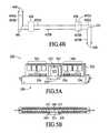
- FIG. 5Ais a front isometric view of a device module that is mated with a motherboard connector, according to an embodiment according to an embodiment of the invention.
- FIG. 5Bis a top view of FIG. 5A , with a substrate of the device module removed from the connector, according to an embodiment of the invention.
- FIG. 5Cis a representative cross-sectional side view of a chip-to-chip connection between a controller and a device module, according to an embodiment of the invention.
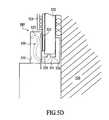
- FIG. 5Dis a close-up of a portion of FIG. 5C delineated by circle G, under an embodiment of the invention.
- FIG. 6illustrate a motherboard connector for mating a device module to a motherboard, under an embodiment of the invention.
- FIGS. 7A-7Cillustrate different embodiments in which device modules are interconnected to one another on a motherboard using bus connections.
- Embodiments of the inventionprovide for high-speed data connectivity and transfer amongst components of motherboards and other substrates.
- Various mechanisms and designsare employed in order to maximize signal integrity, minimize signal degradation, improve transfer speed and control impedance.
- a device modulemay be used to carry a plurality of devices, such as memory devices or other components.
- the device modulemay include a board, a first set of contact points, and a second set of contact points.
- a plurality of signal pathsmay be provided on the board, where each signal path extends between a contact point in the first set and a contact point in the second set.
- each of the plurality of signal pathshas substantially an identical length and a same number of turns on the board.
- turnmeans a change in direction.
- a turn in a signal pathmay include an elbow, or a 90 degree change in direction.
- a systemfor providing high-speed interconnectivity between a controller and a plurality of memory devices.
- the systemmay include a set of one or more boards upon which a plurality of memory devices are provided.
- the setincludes at least a first board on which at least some of the plurality of memory devices are provided.
- a plurality of signal pathsmay be provided on the first board, where each signal path includes a first set of contact points that interconnect the first board to the controller from a position that is proximate to one of the board's lateral sides.
- a second set of contact pointsmay interconnect the board to another component from another position that is proximate to a second lateral side of the first board.
- Each of the plurality of signal pathshas a substantially identical length and an identical number of turns between a contact point in the first set of contact points and a contact point in the second set of contact points.
- the first device module 120may include a plurality of devices 124 connected to a common module board 122 .
- the second device module 130 and third device module 140may include similar devices that are interconnected by respective boards as well, although the arrangement and particular devices provided on each device board may differ.
- Each device module 120 , 130 , 140may be mounted to the motherboard 115 with a respective board connector 125 , 135 and 145 .
- connector 125is mated to the motherboard 115 and includes a receiving end 127 for a bottom surface 126 of the first device module 120 .
- the connector 125 of device module 120may include a plurality of contact elements 123 that conductively connect selective circuits of the device module 120 to motherboard 115 .
- FIG. 1Bis a top view of FIG. 1A , according to an embodiment of the invention.
- controller 110first device module 120 , second device module 130 , and third device module 140 are mounted to motherboard 115 .
- bus 150(as carried in flex cable 160 ) is used to directly connect controller 110 to first device module 120 , as opposed to traditional interconnectivity structures that may be located within motherboard 115 .
- Each device module 120 , 130 , 140may carry a corresponding series of devices 124 , 134 , 144 on one or both sides of each module board 122 , 132 , 142 for that device module.
- Numerous device configurations, device types, and mountings or on-board connectionsare contemplated by embodiments of the invention for each device module 120 , 130 , 140 . Some of these alternative constructions are described with other embodiments and examples provided herein.
- the device module 200is shown which is configured to promote signal integrity and speed from signal connections made to the device module from a bus.
- the device module 200may include a module board 222 upon which a series of devices (represented by first device 226 , second device 227 and eighth device 228 ) are mounted or otherwise interconnected. Examples of the devices that can be mounted to the module board 222 include memory components (e.g. DRAM devices).
- the module board 222may be referenced by a bottom edge 212 , a top edge 216 , and a pair of lateral sides 218 A and 218 B.
- the bottom edge 212may be the side on which the device module 200 is edge-mounted to a motherboard or other substrate.
- a plurality of contact elements 219may be provided on or near the bottom edge 212 .
- Signal tracesmay interconnect each device 226 - 228 with other devices on the module board 222 , or with the motherboard. As shown, each device 226 - 228 on module board 222 includes a set of trace elements 232 which extend downward to bottom edge 212 .
- a first set of input/output points 230is provided adjacent to lateral side 218 A.
- a second set of input/output points 240is provided adjacent to lateral side 218 B.
- Each of the first set of input/output points 230 and the second set of input/output points 240may connect to a corresponding bus to carry at least some signals to and from another device being interconnected to the device module 200 .
- the signals introduced to the device module 200 by either of the first or second set of input/output points 230 , 240may correspond to more critical or important signals, including those in which speed and signal quality are of importance.
- Each device on the device module 120may receive or transmit signals through either a high or low speed signal line.
- Laterally extending trace elementsare part of trace element paths 235 for carrying high-speed signals. Downward extending trace elements 232 are for less critical signals, such as ground and power. Trace elements paths 235 refer to trace elements that are interconnected by the devices to form a particular path for a signal. As shown by FIG. 2 , the lateral extending trace element paths 235 extend between the first and second sets of input/output points 230 , 240 in a substantially linear fashion. In an embodiment such as shown, the trace element paths 235 contain no turns.
- each trace element 235extends linearly between corresponding input/output points 230 , 240 so as to have the same, or substantially the same length as other trace elements 235 extending between individual input/output points adjacent the lateral sides 218 A, 218 B.
- the resultis that the trace elements are about the same length, and therefore have substantially identical signal conduction properties.
- trace element paths 235extend the signal from the first set of input/output points to a first device 226 , a second device 227 and so forth until eight device 228 receives the signals.
- the signals carried by trace element paths 235may be transitioned out of the device through the second set of input/output points.
- all devices on the board module 222are intended to receive the signals from the first set of input/output traces 230 .
- the same interconnectivitymay be provided in a reverse order by trace element paths 235 when signals from an external component are received from a bus connected to the second set of input/output points 240 .
- the first set of input/output points 230may correspond to the point where signals are outputted onto a bus from the device module 200 .
- flex cable 360is connected to an exterior surface 313 of package substrate 312 .
- the exterior surface 313may be immediately adjacent CPU 314 , so that flex cable 360 can also connect to signal traces on an underside of the CPU 311 .
- flex cable 360includes two layers, where one is for signals, and the other is for ground. Alternatively, a single layer construction may be employed.
- Flex cable 360may be extended on an exterior surface 316 of motherboard 315 .
- flex cable 360may be partially or completely submerged into the substrate that is the motherboard 315 . In either case, the flex cable 360 is extended to connector 330 . In an embodiment such as shown, flex cable 360 is extended to a bottom surface 332 of the connector 330 .
- the second plurality of connector elements 339may serve to extend electrical contact from the signal traces 323 of the module board 322 to trace elements of the motherboard 315 and/or the flex connector 360 .
- the first plurality of connector elements 338may be used to extend high-speed connectivity between flex cable 360 and the device module 320 .
- the second plurality of connector elements 339may be used to extend connectivity from trace elements 323 to non-critical signal lines (e.g. power, ground, low-speed signals) of the flex cable 360 , and/or to the motherboard 315 .
- the first plurality of connector elements 338may include traditional pin connector elements, or traditional connector elements shown by elements 339 of FIG. 3A .
- the traditional connector elementsmay be used, for example, to transfer power, ground, or low-speed signals.
- FIGS. 3A-3Cillustrate flex cable 360 being connected to surface 313 of package substrate 312
- another embodimentmay provide for the flex cable 360 to be extended under the package substrate.
- flex cable 360extends adjacent a bottom surface 317 of the package substrate 312 .
- the flex cable 360may be overlaid on exterior surface 316 of the motherboard 315 , and make contact with package substrate 312 through one of the solder balls 318 .
- FIG. 4Aillustrates a device module design in which a plurality of board leads are arranged on a module board for purpose of facilitating or otherwise enabling faster and better quality connections made from outside signal lines that are connected to a bottom end of a device module.
- Such bottom-end connections to device modulesare normally made when device modules are mated or otherwise connected to motherboards using an edge-mounted motherboard connection. Examples of such edge-mounted motherboard connections are provided with FIGS. 3A and 3B , although just about any type of bottom ended connection to a device module can benefit from an embodiment such as shown by FIG. 4A .
- a series of devicesare mounted or otherwise interconnected on a module board 422 .
- the devices that can be mounted to the module board 422include memory components (e.g. DRAM devices).
- the module board 422may be referenced by a bottom edge 412 , a top edge 416 , and a pair of lateral sides 418 A and 418 B.
- the bottom edge 412may be the side on which the device module 400 is edge-mounted to a motherboard or other substrate. Accordingly, a plurality of contact points 419 may be provided on or near the bottom edge 412 .
- a first set of input/output points 430at or adjacent to bottom edge 412 and lateral side 418 A.
- a second set of input/output points 440is provided at or adjacent to top edge 416 and lateral side 418 B.
- the resultis that the first set of input/output points 430 and the second set of input/output points 440 have approximate corner positioning on the board module 422 , diagonally opposed from one another.
- Each of the first set of input/output points 430 and the second set of input/output points 440may connect to a corresponding bus to carry at least some signals to and from another device being interconnected to the device module 400 .
- the signals introduced to the device module 400 by either of the first or second set of input/output points 430 , 440may correspond to more critical or important signals, including those in which speed and signal quality or of importance.
- Downward directed trace elements 419may carry less critical signals, such as power and ground.
- each trace element 435while being described as continuous, may in fact be segmented by individual devices 426 - 428 .
- the individual devices 426 - 428may act as both termination and starting points (left and right sides of the devices) for each segment of a trace element path 435 .
- each trace element path 435 that initiates at input/output point 430traverses across the board module 422 with no more than two turns or elbows. At a first elbow 431 or turn, each trace element path 435 is directed from a vertical direction into a lateral direction. These trace elements paths 435 are extended to each device 426 - 428 linearly, in the lateral direction. Moreover, the effective length of each trace element path as it is extended to each device 426 - 428 and across the board module 422 is about the same length.
- FIG. 4Bis a representative drawing that illustrates trace element paths 435 A, 435 B on device element 400 , according to an embodiment.
- devices 426 , 428are shown in phantom.
- Segments of trace element paths 435 A, 435 B drawn in solidrepresent trace element segments on the module board 422 .
- Segments of trace element paths 435 A, 435 B drawn in phantomillustrate where devices intercept signals of trace element segments and forward the signals onto another trace element segment of the respective trace element paths 435 A, 435 B.
- each trace element path 435 A, 435 Bgoes through an inward and outward bend in between the first and second plurality of input/output points 430 , 440 .
- trace element path 435 Ais about or substantially the same length on device module 400 as trace element path 435 B. Because the trace element paths 435 A and 435 B are substantially the same length, skew amongst different signal paths is minimized or eliminated. This allows high-speed data to be transmitted.
- the device 426may be configured to receive trace element paths 435 A, 435 B in a slightly staggered alignment.
- the staggered alignmentenables signals carried by trace elements 435 A, 435 B to be received by device 426 at about the same time.
- Signals transmitted from device 426 to input points 430may also arrive at the input points 430 at about the same time as a result of the staggered alignment of the trace element paths 435 A, 435 B. This is shown by contact point 455 B of trace element 435 B being further within device 426 than a contact point 455 A of trace element path 435 A.
- a similar staggered arrangementmay be provided for connecting device 428 to the trace elements 435 A, 435 B.
- a side of device 428 proximate to input/output points 440may connect to segments of trace element paths 435 A, 435 B in a staggered alignment, so that the segments of the trace element paths 435 A, 435 B between the device 428 and the input/output points 440 are about the same length.
- FIG. 5Ais a front isometric view of a device module 520 that is mated with a motherboard connector 530 .
- the assemblymay be provided on a motherboard (not shown in this figure).
- a flex cable 560( FIG. 5B ) may be provided on an interior surface 535 ( FIG. 5B ) of the connector 530 .
- the function of the hub package 525includes interconnecting the first set of devices 542 and the second set of devices 544 through a connection made to the hub package 525 .
- Each device in the first set of devices 542 and in the second set of devices 544includes a set of trace elements 536 which extend downward to the connector 530 .
- These trace elements 536may either extend to the motherboard or to a position where the flex cable 560 is mated. The latter would be the case primarily for the hub package 525 .
- Trace elements that mate with the motherboardmay be reserved for power, ground, or low-speed signal elements.
- Trace elements that interconnect with the hub device 525 (now shown), or alternatively with the flex cable 560may be reserved for signals that are desired for high-speed transfer.
- another motherboard component(such as a controller 510 in FIG. 5C ) can be directly connected to the hub package 525 .
- the hub package 525in turn interconnects the other motherboard component to the other devices on the device module 520 .
- the connection to the hub package 525may be made directly with a bus (e.g. as provided by flex connector 560 ) that extends from the other motherboard component, rather than other traditional techniques (such as using motherboard vias).
- FIG. 5A and 5Bshows a push-pin construction that aligns flex cable 560 in making contact with contact points on an exterior surface of the package substrate 524 .
- a traditional mechanical fastenersuch as a screw or clamp may make the active connection when alignment is achieved with the push-pins.
- the push-pinsmay provide both alignment and an active force.
- a pair of push pins 540are shown that extend into an interior cavity 536 of connector 530 .
- the push pins 540may serve as an alignment mechanism by aligning with and inserting into corresponding apertures 539 .
- a traditional fastenersuch as a screw or clamp may be used to secure the package substrate 524 against the leads of the flex cable at precise contact points on the package substrate.
- FIG. 5Cis a representative cross-sectional side view of a chip-to-chip connection between a controller 510 and a device module 520 .
- flex cable 560is extended from a direct connection of a CPU 514 of controller 510 to hub device 523 .
- the flex cable 560may be fixed, suspended or submerged with respect to motherboard 515 .
- a securement mechanism 580(shown by circle G) may be used to actively contact leads on the flex connector 560 with contact points on the package substrate 524 . This creates a direct contact between controller 510 and hub device 523 .
- FIG. 5Dis a close-up of circle G, illustrating a securement mechanism 580 , under an embodiment of the invention.
- Securement mechanism 580may include an S-shaped contact element 550 is embedded within an insulative section 555 of connector 530 .
- a tail 556 of the contact elementprotrudes from a bottom surface 551 of the cavity 536 .
- the tail 556is moveable downward so as to become flush with bottom surface 551 . This in turn causes the contact element 550 to rock or otherwise move clockwise.
- the contact element 550may have a contact section 552 of that member presses against the flex cable 560 and creates an active force between individual signal lines of the flex cable and a corresponding trace element 523 on the package substrate 524 .
- the trace element 523 on the package substrate 524may correspond to gold (or other conductive element) dots.
- FIGS. 5A-5Ddescribe specific mechanism by which an active engagement is created for extending and connecting a bus carried in a flex cable directly to a device on a substrate of a device module
- securement mechanism 580may include an embedded roller that contracts upon the entrance of a substrate, then expands to force a flex cable into contact with contact points on the substrate.
- a flex cablemay be provided with a specific type of connector described in U.S. patent application Ser. No. 10/608,255, entitled ARRAY CONNECTOR WITH DEFLECTABLE COUPLING STRUCTURE FOR MATING WITH OTHER COMPONENTS, filed Jun. 27, 2003.
- the aforementioned applicationis hereby incorporated by reference in its entirety.
- FIG. 6illustrate a motherboard connector for mating a device module to a motherboard, under an embodiment of the invention.
- a connectorsuch as described with FIG. 6 may be used with, for example, embodiments shown and described with FIGS. 3A and 3B .
- FIG. 6is partial, side cross-sectional view of a segment 632 of a connector 630 .
- the connector 630includes a motherboard contact surface 602 .
- the segment 632may form a portion of an opening 636 in which an edge of a board module (or other substrate end) is received.
- a body 638 of the connector 600may be formed by insulative materials.
- a series of connector tunnels 610may be formed with the body 638 .
- FIG. 6illustrates one connector tunnel 610 and connector member 615 . Additional tunnels and connector members may be assumed to be similarly formed in the body 638 in a direction extending into and out of the paper.
- Connector membermay be provided a contact point 612 in an opening 622 formed on an interior side 624 of the opening 636 .
- the contact point 612is hooked or bent in a reverse-C or partial U-shape. The result is that contact point 612 is rounded.
- the opening 622is sufficiently large to enable the contact point 612 to engage, deflect and pivot, flex, and/or allow wipe, or otherwise move about.
- connector tunnel 610 and connector member 615are configured to reduce an overall length that a signal must travel form motherboard to contact point 612 . Accordingly, a shaft 614 of connector member 615 is substantially linear.
- contact point 612is moved counterclockwise, or towards an interior surface 621 of the opening 622 .
- contact point 612is moved inward by the substrate, it resiliently presses back against the substrate.
- the substratemay be aligned so that a corresponding contact point on the substrate contacts contact point 621 .
- An electrical connectioncan then be made.
- the same mechanismcan be used to make similar electrical connections for a series of connector members distributed axially (into and out of the paper) within the body 638 .
- the manner in which connector 630 is formedis that connector tunnel 610 is formed to accommodate a shape, length and angle of the connector member 615 . Since the connector tunnel 610 and the connector member 615 are both substantially linear, it is relatively easy to insert connector member 615 into a corresponding tunnel. A tail end 619 of the connector member 615 is inserted into the tunnel first, until the tail end protrudes slightly within a tail opening 644 . The tail end 619 will, when connector 630 is mated with a motherboard, make contact with a corresponding conductive element on the motherboard.
- center section 611may pivot within the body 638 .
- a protrusion or other elementmay be provided centrally within the tunnel 610 . That region of the tunnel 610 may be slightly larger than a cross-section of the connector element, but the protrusion may prevent the connector member from being easily slid out of the connector tunnel 610 . The result is that connector member 615 is moveable within connector tunnel 610 .
- Edge-mounted device modulesmay be combined together on motherboards in various arrangements. For example, such modules may be interconnected in series for purpose of communicating with one other motherboard component or controller.
- FIGS. 7A-7Cillustrate different embodiments in which multiple device modules are interconnected.
- a controller 710having a CPU 714 and substrate 712 , are mounted to a first section of a motherboard 715 .
- Multiple (two or more) device modules 720 , 730are positioned across from the controller 710 on the motherboard 715 , using motherboard connectors.
- the motherboard connectorsmay be convention, or as described in FIGS. 3A, 3B and 6 .
- a busmay interconnect controller 710 with the first device module 720 , and then with the second device module 730 in series.
- the busmay be extended with a flex cable 760 .
- the flex cable 760may be of a rigid-flex connection.
- the first device module 720is provided the flex cable 760 as an integral (permanently fixed) component.
- a side mount(such as described by FIGS. 1A, 1B and 2 ) may be used to join the flex cable 760 with the first device module 720 .
- Each flex cable to device module connectionmay be accomplished through a side connection, as described with embodiments in FIG. 1 and 1 B.
- front and back faces of each device module 710 , 720 and 730may have trace element path designs to facilitate high-speed data transfer and side mounted flex cables. Such designs are describe with FIG. 2 , and elsewhere in the application.
Landscapes
- Engineering & Computer Science (AREA)
- Microelectronics & Electronic Packaging (AREA)
- Combinations Of Printed Boards (AREA)
Abstract
Description
- This invention relates generally to the data busses. More particularly, the invention relates to the field of high-speed interconnectivity amongst motherboard components.
- Computer components such as memory are typically accessible from different locations in any given system. On a computer motherboard, for example, a Level 1 cache is located on the IC chip, while the Level 2 cache is frequently located in nearby modules. To access the main memory, an electrical or electronic buss is commonly used to transmit signals between the CPU and the main memory of the computer, or as the case may be, of the video module or plug-in card. In practice, the speed or performance of a computer (or of the video module or plug-in card) is very often more limited by capabilities of the buss between memory and CPU and its design, than by the operating speed of the microprocessor.
- Traditional approaches to memory buss structures and methods for their creation have thus far been limited to the use of circuit traces that are an integral part of the circuit board that interconnects the memory modules to the CPU. This has not been a significant matter of concern in the past, because memory devices operated fairly slowly. With newer memory architectures, however, it is possible to run memory much faster, but even this improvement has been impeded by buss design. Thus, the full capabilities of the memory components are typically not achieved.
FIG. 1A illustrates a system where a bus is directly connected to a device module in order to enable direct communication between a motherboard component and that device module, according to an embodiment.FIG. 1B is a top view ofFIG. 1A .FIG. 2 illustrates a device module design in which a plurality of board leads are arranged on a module board for purpose of facilitating or otherwise enabling faster and better quality connections to be made with the device module.FIGS. 3A and 3B are cross-sectional views of alternative embodiments in which a controller or other motherboard component is interconnected with a device module using a high-speed connection.FIG. 4A illustrates a device module design in which a plurality of board leads are arranged on a module board for purpose of facilitating or otherwise enabling faster and better quality connections made form outside signal lines that are connected to a bottom end or portion of a device module.FIG. 4B is a representative drawing illustrating a design of trace element paths on a device module, according to an embodiment of the invention.FIG. 5A is a front isometric view of a device module that is mated with a motherboard connector, according to an embodiment according to an embodiment of the invention.FIG. 5B is a top view ofFIG. 5A , with a substrate of the device module removed from the connector, according to an embodiment of the invention.FIG. 5C is a representative cross-sectional side view of a chip-to-chip connection between a controller and a device module, according to an embodiment of the invention.FIG. 5D is a close-up of a portion ofFIG. 5C delineated by circle G, under an embodiment of the invention.FIG. 6 illustrate a motherboard connector for mating a device module to a motherboard, under an embodiment of the invention.FIGS. 7A-7C illustrate different embodiments in which device modules are interconnected to one another on a motherboard using bus connections.- In the drawings, the same reference numbers identify identical or substantially similar elements or acts. Any modifications necessary to the Figures can be readily made by one skilled in the relevant art based on the detailed description provided herein.
- A. Overview
- Embodiments of the invention provide for high-speed data connectivity and transfer amongst components of motherboards and other substrates. Various mechanisms and designs are employed in order to maximize signal integrity, minimize signal degradation, improve transfer speed and control impedance.
- According to an embodiment, a device module is provided. The device module may be used to carry a plurality of devices, such as memory devices or other components. The device module may include a board, a first set of contact points, and a second set of contact points. A plurality of signal paths may be provided on the board, where each signal path extends between a contact point in the first set and a contact point in the second set. According to an embodiment, each of the plurality of signal paths has substantially an identical length and a same number of turns on the board.
- As used herein, the term “substantially an identical length” in the context of two or more signal paths means that each signal path carries signals that when started and terminated at identical points on a straight line, have skew that is less than or equal to one-fourth the operational frequency of the system that generated the signals.
- In another embodiment, a device module is provided having a board and a plurality of devices. In one embodiment, the device module includes at least one set of signal paths that have no turns. In another embodiment, the device module includes at least one set of signal paths that individually have two or fewer number of turns. In either embodiment, the overall length of the signal paths on the board are substantially identical.
- As used herein, the term “signal path” means the path of a signal generated from one source and communicated directly or indirectly to another device. It is understood that the signal can be intercepted or otherwise processed by one or more intermediary devices
- The term “turn” means a change in direction. For example, a turn in a signal path may include an elbow, or a 90 degree change in direction.
- In another embodiment, a system is described for providing high-speed interconnectivity between a controller and a plurality of memory devices. The system may include a set of one or more boards upon which a plurality of memory devices are provided. The set includes at least a first board on which at least some of the plurality of memory devices are provided. A plurality of signal paths may be provided on the first board, where each signal path includes a first set of contact points that interconnect the first board to the controller from a position that is proximate to one of the board's lateral sides. A second set of contact points may interconnect the board to another component from another position that is proximate to a second lateral side of the first board. Each of the plurality of signal paths has a substantially identical length and an identical number of turns between a contact point in the first set of contact points and a contact point in the second set of contact points.
- B. Direct Connection to Device Modules
FIG. 1A illustrates an embodiment in which a controller110 (or other motherboard component) is directly connected to a device module. In an embodiment such as shown byFIG. 1 ,controller 110 is directly connected to afirst device module 120. The connection with thefirst device module 120 interconnects thecontroller 110 to a series of devices modules. For example, inFIG. 1 ,controller 110 controls and otherwise communicate withsecond device module 130 andthird device module 140 through the connection with thefirst device module 120. In one application, eachdevice module controller 110 may correspond to a memory controller for the series of memory modules. For example, eachdevice module - The
controller 110 may include apackage substrate 112 and aCPU 114. TheCPU 114 is mounted onto thepackage substrate 112. TheCPU 114 may be conductively mounted using conductive balls, points or pins. Thepackage substrate 112 is shown as being electrically connected tomotherboard 115 usingsolder balls 118, although other forms of conductive connections such as pins, points, wires, wire bondings, or any other integrated circuit interconnection technology may also be used. Thesolder balls 118 may make one or more connection leads from thepackage substrate 112 to themotherboard 115. - The
first device module 120 may include a plurality ofdevices 124 connected to acommon module board 122. Thesecond device module 130 andthird device module 140 may include similar devices that are interconnected by respective boards as well, although the arrangement and particular devices provided on each device board may differ. Eachdevice module motherboard 115 with arespective board connector first device module 120,connector 125 is mated to themotherboard 115 and includes a receivingend 127 for abottom surface 126 of thefirst device module 120. Theconnector 125 ofdevice module 120 may include a plurality ofcontact elements 123 that conductively connect selective circuits of thedevice module 120 tomotherboard 115. Thesecond device module 130 and thethird device module 140 may be similarly connected tomotherboard 115 usingrespective connectors contact elements 123 may be bent or otherwise non-linear when extending frommotherboard 115 tomodule board 122. Under an embodiment such as shown withFIGS. 3A-3C , at least some of the plurality ofcontact elements 123 are substantially linear, so as to preserve signal integrity and promote transfer speed. Specific examples of such connectors for use with such embodiments are provided withFIG. 6 . - Multiple signal lines have to be carried from the
controller 110 to thefirst device module 120 in order to communicatively couple the controller to the first device module. Under traditional approaches, signal line connections between thecontroller 110 and thedevice module 120 are made by extending the signal lines inside themotherboard 115. This typically requires forming a series of interconnected vias for thecontroller 110 to themotherboard 115, and corresponding vias for theconnector 125 offirst device module 120 to themotherboard 115. The result is the signal lines from thecontroller 110 and themodule board 122 are interconnected using a “via-to-via” connection from within the motherboard. This approach is problematic for several reasons. Forming vias within a motherboard has additional costs and expenses. Furthermore, there is a limited amount of space on the motherboard, and if extended via formations can be avoided, there is benefit. Lastly, vias by nature are a source of signal reflection, unwanted inductance, and signal degradation. - While the
controller 110 and thedevice modules motherboard 115, an embodiment described herein provides forcontroller 110 to connect tofirst device module 120 using abus 150 that eliminates, or at least substantially reduces, the need for making the connection using vias internal to or on the surface of themotherboard 115. In one embodiment, bus50 is carried by aflex cable 160 that connects to signal traces on thepackage substrate 112 and to signal traces on themodule board 122. In another embodiment, thebus 150 is traced, overlaid, or otherwise presented on the outside ofmotherboard 115. As will be described, withFIGS. 2A and 2B , the location of the connection between thebus 150 and themodule board 122 facilitates high-speed signal transfer. Furthermore, the manner in which the connection incoming signal lines frombus 150 are received on themodule board 122 of thefirst device module 120 enables high-speed data transfer with little signal degradation, with all signal ines or paths being of equal length. - In an arrangement where multiple device modules are used, a
second bus 152 may connect signal lines onfirst device module 120 with signal lines onsecond device module 130. Similarly, athird bus 154 may connect signal lines onsecond device module 130 with signal lines onthird device module 140. As illustrated withFIGS. 7A and 7B , thesecond bus 152 and thethird bus 154 may be carried in corresponding flex cables that can be serpentined between the series ofdevice modules - In contrast to past and current approaches, an embodiment such as shown in
FIGS. 1A and 1B avoids connecting signal lines on thepackage substrate 112 andmodule board 122 using “via-to-via” interconnections. Making a direct connection todevice module 120 usingbus 150 avoids signal degradation issues and other problems associated with traditional approaches for making such connections. A faster and better quality connection is made using a construction such as described, where buses external tomotherboard 115 substitute for the use of vias. FIG. 1B is a top view ofFIG. 1A , according to an embodiment of the invention. In an example shown byFIG. 1B ,controller 110,first device module 120,second device module 130, andthird device module 140 are mounted tomotherboard 115. However, bus150 (as carried in flex cable160) is used to directly connectcontroller 110 tofirst device module 120, as opposed to traditional interconnectivity structures that may be located withinmotherboard 115. Eachdevice module devices module board device module - As shown,
signal lines 163 onpackage substrate 112 are connected tobus 150, which carried by aflex cable 160. Eachdevice module motherboard 115 on its bottom surface. With respect tofirst device module 120,flex cable 160 extendsbus 150 to alateral side 121A. Signal traces for thefirst device module 120 may be provided at or adjacent tolateral side 121A for purpose of connectingfirst device module 120 tocontroller 110. Asecond flex cable 162 may carry a second bus between signal traces provided onlateral side 121B offirst device module 120, and signal traces provided on alateral side 131A ofsecond device module 130. Athird flex cable 164 may carry a third bus between signal lines provided on alateral side 131B ofsecond device module 130, and signal lines provided on alateral side 141A ofthird device module 140. In a serpentine configuration, additional device modules may be added, and interconnected using the side-connected bus.FIG. 2B illustrates a suitable device module construction for enabling side-connected buses to be connected to the device modules. - While embodiments such as shown by
FIGS. 1A and 1B illustrate thatflex cable 160 floats abovemotherboard 115 when extendingbus 150 frompackage substrate 112 tomodule board 122, it should be noted that there are other ways to carry thebus 150. For example, theflex cable 160 may be affixed to a portion of themotherboard 115 between thepackage substrate 112 and themodule board 122. As another example, signal lines may be at least partially carried frompackage substrate 112 to themodule board 122, without use of a flex cable. - Furthermore, while embodiments described in
FIGS. 1A and 1B , as well as elsewhere in this application, describe thecontroller 110 as directly connecting to thefirst device module 120 usingbus 150, it may also be the case thatbus 150 provides only one of two or more connections between the controller and theparticular device module 120. Specifically,controller 110 may still include leads that are electrically coupled to the first device module120 (or second orthird device modules 130,140) through a series of vias provided inmotherboard 115. In one embodiment, not all signal lines thatfirst device module 120 needs to receive communications fromcontroller 110 are carried inbus 150. For example, power and ground lines (which have significantly less speed and quality requirements) may still be provided frommotherboard 115 throughconnector 125. It is also possible to extend multiple busses such as described withbus 150 betweencontroller 110 and one or more of thedevice modules - Also, while embodiments described with
FIGS. 1A and 1B illustrate use of three device modules provided on a motherboard, more or fewer device modules may be used. For example, it may be possible to mount tens or even hundreds of device modules using techniques such as described inFIGS. 1A, 1B or elsewhere in the application. - C. Device Module Design for Direct Connection with Another Motherboard Component
FIG. 2 illustrates a device module design in which a plurality of board leads are arranged on a module board for purpose of facilitating or otherwise enabling faster and better quality connections to be made with the device module. In particular, device module designs such as described inFIG. 2 may be used to receive a bus in a direct board connection with that device module, as described with embodiments ofFIGS. 1A and 1B .- With reference to
FIG. 2 , adevice module 200 is shown which is configured to promote signal integrity and speed from signal connections made to the device module from a bus. Thedevice module 200 may include amodule board 222 upon which a series of devices (represented byfirst device 226,second device 227 and eighth device228) are mounted or otherwise interconnected. Examples of the devices that can be mounted to themodule board 222 include memory components (e.g. DRAM devices). Themodule board 222 may be referenced by abottom edge 212, atop edge 216, and a pair oflateral sides bottom edge 212 may be the side on which thedevice module 200 is edge-mounted to a motherboard or other substrate. Accordingly, a plurality ofcontact elements 219 may be provided on or near thebottom edge 212. Signal traces may interconnect each device226-228 with other devices on themodule board 222, or with the motherboard. As shown, each device226-228 onmodule board 222 includes a set of trace elements232 which extend downward tobottom edge 212. - In an embodiment, a first set of input/
output points 230 is provided adjacent tolateral side 218A. A second set of input/output points 240 is provided adjacent tolateral side 218B. Each of the first set of input/output points 230 and the second set of input/output points 240 may connect to a corresponding bus to carry at least some signals to and from another device being interconnected to thedevice module 200. The signals introduced to thedevice module 200 by either of the first or second set of input/output points device module 120 may receive or transmit signals through either a high or low speed signal line. Laterally extending trace elements are part oftrace element paths 235 for carrying high-speed signals. Downward extending trace elements232 are for less critical signals, such as ground and power.Trace elements paths 235 refer to trace elements that are interconnected by the devices to form a particular path for a signal. As shown byFIG. 2 , the lateral extendingtrace element paths 235 extend between the first and second sets of input/output points trace element paths 235 contain no turns. The result is that eachtrace element 235 extends linearly between corresponding input/output points other trace elements 235 extending between individual input/output points adjacent the lateral sides218A,218B. The result is that the trace elements are about the same length, and therefore have substantially identical signal conduction properties. - In contrast, prior art approaches includes turns in the trace element paths for both critical and non-critical signals. The inclusion of turns to adjust lengths of the signal traces results in added real-estate on the surface of the board module. However, the inclusion of turns in signal traces creates skew, in that some signal paths are longer than others. Also, reflection may exist as a result of impedance resulting from the turns in the signal paths. Under an embodiment such as described by
FIG. 2 , thetrace element paths 235 extending to and from devices have the same or equivalent lengths, thereby equalizing impedance amongst signal traces. Furthermore, signal paths with equal lengths minimize or eliminating skew amongst signal traces and paths. - For a given signal received through a bus that is connected to the first set of input/
output points 230,trace element paths 235 extend the signal from the first set of input/output points to afirst device 226, asecond device 227 and so forth until eightdevice 228 receives the signals. In this direction, the signals carried bytrace element paths 235 may be transitioned out of the device through the second set of input/output points. This assumes that all devices on theboard module 222 are intended to receive the signals from the first set of input/output traces230. The same interconnectivity may be provided in a reverse order bytrace element paths 235 when signals from an external component are received from a bus connected to the second set of input/output points240. In this direction, the first set of input/output points 230 may correspond to the point where signals are outputted onto a bus from thedevice module 200. - While an embodiment such as described with
FIG. 2 illustrates devices that are arranged to receive signals from the first set of input/output points 230 in series, other embodiments may provide for other patterns or means for distributing the signals from the bus. For example, the first device that receive signals from input/output points 230 may include an intermediate hub device (see e.g.FIG. 5A ), which distributes signals to adjacent devices on theboard module 222. Alternatively, more than one device can directly receive signals from the first set of input/output points230. - D. Connector Connection for Device Module
FIGS. 3A and 3B are cross-sectional views of alternative embodiments in which a controller or other motherboard component is interconnected with a device module using a high-speed connection. As with embodiments described withFIGS. 1A and 1B , an embodiment such as described withFIG. 3A avoids (or reduces) the need for “via-to-via” connections between the motherboard component and the device module. However, unlike embodiments described withFIGS. 1A and 1B , a connection is made to a device module through a connector for mounting the device module to a motherboard.- With reference to
FIG. 3A , acontroller 310 is mounted to a motherboard315. Thecontroller 310 includes aCPU 314 connected to apackage substrate 312. Conductive points, pins or solder balls may be used to interconnect theCPU 314 and thepackage substrate 312. Thedevice module 320 is connected to motherboard315 throughconnector 330. In an example provided byFIG. 3A ,device module 320 includes a module board322 having afront face 326 and aback face 327. Asubstrate package 324, including a CPU325 or other component, is shown on thefront face 326. Anotherdevice 329 may be provided on theback face 327. Signal traces323 for connecting toconnector 330 may be provided on one or bothfaces front face 326 or theback face 327, including in a direction that extends into or out of the paper. In one memory application for example, CPU325 corresponds to a hub device which is accessed as a switch that distributes communications from thecontroller 310 to other memory devices on the module board322. In this example, thedevice 329 on theback face 327 may correspond to a DIMM device. - With respect to the
controller 310,package substrate 312 and motherboard315 may be interconnected bysolder balls 318. Signal traces may be extended fromCPU 314 through microvias inpackage substrate 318. The signal traces may be extended through one or more of the solder balls319 to the motherboard315. However, while thecontroller 310 and motherboard315 are interconnected through various vias and other connective mechanisms, a different type of high-speed connection may be formed between the controller and thedevice module 320. Specifically, the connection between thecontroller 310 anddevice module 320 may be made through a flex cable360 (or similar bus structure) that eliminates, or otherwise reduces the need for vias. - In one,
flex cable 360 is connected to anexterior surface 313 ofpackage substrate 312. Theexterior surface 313 may be immediatelyadjacent CPU 314, so thatflex cable 360 can also connect to signal traces on an underside of theCPU 311. In one embodiment,flex cable 360 includes two layers, where one is for signals, and the other is for ground. Alternatively, a single layer construction may be employed.Flex cable 360 may be extended on anexterior surface 316 of motherboard315. Alternatively,flex cable 360 may be partially or completely submerged into the substrate that is the motherboard315. In either case, theflex cable 360 is extended toconnector 330. In an embodiment such as shown,flex cable 360 is extended to abottom surface 332 of theconnector 330. - The
connector 330 includes an opening336 for receiving the bottom surface321 of thedevice module 320. Theconnector 330 may be substantially u-shaped, with afirst structure 332 adjacent tofront face 326, and a second structure334 adjacent to backface 327. In an embodiment shown byFIG. 3A ,connector 330 is a hybrid connector, in that it includes two kinds of connector elements. In particular, a first plurality ofconnector elements 338 having a first geometric shape may extend through thefirst structure 332. A second plurality ofconnector elements 339, having a second geometric shape, extends through the second structure334. The first plurality ofconnector elements 338 serve to extend electrical contact from the signal traces323 of the module board322 to individual signal lines carried inflex cable 360. The second plurality ofconnector elements 339 may serve to extend electrical contact from the signal traces323 of the module board322 to trace elements of the motherboard315 and/or theflex connector 360. For reasons provided in the following paragraph, the first plurality ofconnector elements 338 may be used to extend high-speed connectivity betweenflex cable 360 and thedevice module 320. The second plurality ofconnector elements 339 may be used to extend connectivity fromtrace elements 323 to non-critical signal lines (e.g. power, ground, low-speed signals) of theflex cable 360, and/or to the motherboard315. - The first plurality of
connector elements 338 are better suited for carrying high-speed signals to thedevice module 320 because of their signal path routing. Specifically, eachconnector element 338 is substantially linear. Moreover, eachconnector element 338 may be optimally angled to shorten an overall length of that connector element. The shorter,straighter connector element 338 minimize or eliminate reflections, thereby controlling impedance, and improving signal quality and speed. In contrast,individual connector elements 339 are curved, or otherwise substantially non-linear. The geometric shape ofconnector elements 339 is one used in some prior art approaches. The curved nature ofconnector elements 339 results in reflection and uncontrolled impedance, thereby resulting in signal degradation. FIG. 3B illustrates a design that uses an alternative connector for connectingflex cable 360 todevice module 320. In particular,connector 360 may be equipped with first and second plurality ofconnector elements 338, where some or all of theconnector elements 338 have a common geometric shape. This geometric shape is, as described withFIG. 3A , substantially linear. In addition, connector elements on thefirst structure 332 and second structure334 may be optimally angled to minimize an overall length of the connector element as it extends from the motherboard315 to traceelements 323 on the module board322. The benefits for having linear and angled connector elements described inFIG. 3A or applicable to both first andsecond connector elements 338 shown inFIG. 3B .- As
FIGS. 3A and 3B are both cross-sectional views, it should be notes that not all of the individual connector elements in either the first or second plurality of connector elements need to have the same geometric shape, or even be of the same kind. For example, with reference to embodiments described in eitherFIG. 3A orFIG. 3B , the first plurality ofconnector elements 338 may include traditional pin connector elements, or traditional connector elements shown byelements 339 ofFIG. 3A . The traditional connector elements may be used, for example, to transfer power, ground, or low-speed signals. - While an embodiment such as shown by
FIGS. 3A-3C illustrateflex cable 360 being connected to surface313 ofpackage substrate 312, another embodiment may provide for theflex cable 360 to be extended under the package substrate. In this configuration,flex cable 360 extends adjacent abottom surface 317 of thepackage substrate 312. Theflex cable 360 may be overlaid onexterior surface 316 of the motherboard315, and make contact withpackage substrate 312 through one of thesolder balls 318. - D. Device Module Design for Facilitating High-Speed Connection with Device Connector and Bus
FIG. 4A illustrates a device module design in which a plurality of board leads are arranged on a module board for purpose of facilitating or otherwise enabling faster and better quality connections made from outside signal lines that are connected to a bottom end of a device module. Such bottom-end connections to device modules are normally made when device modules are mated or otherwise connected to motherboards using an edge-mounted motherboard connection. Examples of such edge-mounted motherboard connections are provided withFIGS. 3A and 3B , although just about any type of bottom ended connection to a device module can benefit from an embodiment such as shown byFIG. 4A .- With reference to
FIG. 4A , a series of devices (represented byfirst device 426,second device 427 and eighth device428) are mounted or otherwise interconnected on a module board422. Examples of the devices that can be mounted to the module board422 include memory components (e.g. DRAM devices). The module board422 may be referenced by abottom edge 412, a top edge416, and a pair oflateral sides bottom edge 412 may be the side on which the device module400 is edge-mounted to a motherboard or other substrate. Accordingly, a plurality of contact points419 may be provided on or near thebottom edge 412. - In an embodiment, a first set of input/
output points 430 at or adjacent tobottom edge 412 andlateral side 418A. A second set of input/output points 440 is provided at or adjacent to top edge416 andlateral side 418B. The result is that the first set of input/output points 430 and the second set of input/output points 440 have approximate corner positioning on the board module422, diagonally opposed from one another. Each of the first set of input/output points 430 and the second set of input/output points 440 may connect to a corresponding bus to carry at least some signals to and from another device being interconnected to the device module400. The signals introduced to the device module400 by either of the first or second set of input/output points trace elements 419, on the other hand, may carry less critical signals, such as power and ground. - Signal traces may interconnect each device426-428 with other devices on the module board422, or with the motherboard. In an embodiment such as shown by
FIG. 4A , each device426-428 is interconnected to other devices or to the motherboard by trace elements that extend in one of two directions. These directions include a downward direction and a lateral direction. Downward extendingtrace elements 419 extend to or nearbottom edge 412 and terminate at contact points419. Lateral extending trace elements435 follow substantially lateral paths between the first and second set of input/output points elbows - An embodiment such as shown by
FIG. 4A enables bottom connections to be made to the device module400, while at the same time preserving signal integrity and speed. In an embodiment such as shown byFIG. 4A , each trace element path435 that initiates at input/output point 430 traverses across the board module422 with no more than two turns or elbows. At afirst elbow 431 or turn, each trace element path435 is directed from a vertical direction into a lateral direction. These trace elements paths435 are extended to each device426-428 linearly, in the lateral direction. Moreover, the effective length of each trace element path as it is extended to each device426-428 and across the board module422 is about the same length. FIG. 4B is a representative drawing that illustratestrace element paths devices trace element paths trace element paths trace element paths FIG. 4B , eachtrace element path output points trace element path 435A is about or substantially the same length on device module400 astrace element path 435B. Because thetrace element paths - In order to match the overall length of the trace element path from a side of
device 426 that is proximate to the input/output points 430, thedevice 426 may be configured to receivetrace element paths trace elements device 426 at about the same time. Signals transmitted fromdevice 426 to inputpoints 430 may also arrive at the input points430 at about the same time as a result of the staggered alignment of thetrace element paths contact point 455B oftrace element 435B being further withindevice 426 than acontact point 455A oftrace element path 435A. A similar staggered arrangement may be provided for connectingdevice 428 to thetrace elements device 428 proximate to input/output points 440 may connect to segments oftrace element paths trace element paths device 428 and the input/output points 440 are about the same length. - Direct Chip-To-Chip Connection Between Motherboard Component and Device on Board Module
- While embodiments such as described by
FIGS. 3A and 3B provide for extending a cable to connector elements of a connector on a motherboard in order to interconnect a motherboard component with a device module, other embodiments may provide for extending the flex cable (or other integrated bus structure) through the connector so as to make a direct connection with an element of a device module.FIG. 5A is a front isometric view of adevice module 520 that is mated with amotherboard connector 530. The assembly may be provided on a motherboard (not shown in this figure). A flex cable560 (FIG. 5B ) may be provided on an interior surface535 (FIG. 5B ) of theconnector 530. Thedevice module 520 may include ahub package 525, which comprises ahub device 523 provided on apackage substrate 524. Thepackage substrate 524 in turn is connected to amodule board 522. A first set ofdevices 542 extend to the left of thehub package 525. A second set ofdevices 544 extend to the right of thehub package 525. - In one application, the function of the
hub package 525 includes interconnecting the first set ofdevices 542 and the second set ofdevices 544 through a connection made to thehub package 525. Each device in the first set ofdevices 542 and in the second set ofdevices 544 includes a set oftrace elements 536 which extend downward to theconnector 530. Thesetrace elements 536 may either extend to the motherboard or to a position where theflex cable 560 is mated. The latter would be the case primarily for thehub package 525. Trace elements that mate with the motherboard may be reserved for power, ground, or low-speed signal elements. Trace elements that interconnect with the hub device525 (now shown), or alternatively with theflex cable 560, may be reserved for signals that are desired for high-speed transfer. - In an embodiment such as shown by
FIGS. 5A and 5B , another motherboard component (such as acontroller 510 inFIG. 5C ) can be directly connected to thehub package 525. Thehub package 525 in turn interconnects the other motherboard component to the other devices on thedevice module 520. In contrast to past approaches, the connection to thehub package 525 may be made directly with a bus (e.g. as provided by flex connector560) that extends from the other motherboard component, rather than other traditional techniques (such as using motherboard vias). - As with previously described embodiments, the set of
trace elements 536 may utilize traditional connectivity to connect to trace elements on the underlying motherboard. Connectivity betweenhub package 525 and theflex connector 560 may use another mechanism.FIG. 5B is a top view ofconnector 530, showingflex cable 560 extended to a position that will cause elements offlex cable 560 to mate with trace elements on thepackage substrate 524. In one embodiment,hub package 525 is positioned so thatpackage substrate 524 contacts aninterior surface 531 ofconnector 530. - Various mechanisms for accomplishing a direct “chip-to-chip” connection between a motherboard component (e.g. controller510) and
hub package 525 using a bus (such as flex connector560) have been described in U.S. patent application Ser. No. 10/426,930, entitled DIRECT-CONNECT SIGNALING SYSTEM, filed Apr. 29, 2003. The aforementioned patent application is hereby incorporated by reference in its entirety for all purposes. With reference toFIG. 5B , an active contact may be made betweenflex cable 560 and trace elements onpackage substrate 524. An embodiment ofFIGS. 5A and 5B , for example, shows a push-pin construction that alignsflex cable 560 in making contact with contact points on an exterior surface of thepackage substrate 524. A traditional mechanical fastener, such as a screw or clamp may make the active connection when alignment is achieved with the push-pins. Alternatively, the push-pins may provide both alignment and an active force. - With reference to
FIG. 5B , a pair of push pins540 are shown that extend into aninterior cavity 536 ofconnector 530. The push pins540 may serve as an alignment mechanism by aligning with and inserting intocorresponding apertures 539. A traditional fastener, such as a screw or clamp may be used to secure thepackage substrate 524 against the leads of the flex cable at precise contact points on the package substrate. FIG. 5C is a representative cross-sectional side view of a chip-to-chip connection between acontroller 510 and adevice module 520. As shown,flex cable 560 is extended from a direct connection of a CPU514 ofcontroller 510 tohub device 523. Theflex cable 560 may be fixed, suspended or submerged with respect to motherboard515. A securement mechanism580 (shown by circle G) may be used to actively contact leads on theflex connector 560 with contact points on thepackage substrate 524. This creates a direct contact betweencontroller 510 andhub device 523.FIG. 5D is a close-up of circle G, illustrating asecurement mechanism 580, under an embodiment of the invention.Securement mechanism 580 may include an S-shapedcontact element 550 is embedded within aninsulative section 555 ofconnector 530. When nodevice module 520 is inserted, atail 556 of the contact element protrudes from abottom surface 551 of thecavity 536. Whenboard module 522 is inserted into thecavity 536, thetail 556 is moveable downward so as to become flush withbottom surface 551. This in turn causes thecontact element 550 to rock or otherwise move clockwise. Thecontact element 550 may have acontact section 552 of that member presses against theflex cable 560 and creates an active force between individual signal lines of the flex cable and acorresponding trace element 523 on thepackage substrate 524. In one embodiment, thetrace element 523 on thepackage substrate 524 may correspond to gold (or other conductive element) dots.- While
FIGS. 5A-5D describe specific mechanism by which an active engagement is created for extending and connecting a bus carried in a flex cable directly to a device on a substrate of a device module, other embodiments may provide different mechanisms for creating the active engagement. For example,securement mechanism 580 may include an embedded roller that contracts upon the entrance of a substrate, then expands to force a flex cable into contact with contact points on the substrate. As an alternative, a flex cable may be provided with a specific type of connector described in U.S. patent application Ser. No. 10/608,255, entitled ARRAY CONNECTOR WITH DEFLECTABLE COUPLING STRUCTURE FOR MATING WITH OTHER COMPONENTS, filed Jun. 27, 2003. The aforementioned application is hereby incorporated by reference in its entirety. - Connector for Extending High-Speed Connection from Motherboard to Edge-Mounted Device Module
FIG. 6 illustrate a motherboard connector for mating a device module to a motherboard, under an embodiment of the invention. A connector such as described withFIG. 6 may be used with, for example, embodiments shown and described withFIGS. 3A and 3B .FIG. 6 is partial, side cross-sectional view of asegment 632 of aconnector 630. Theconnector 630 includes amotherboard contact surface 602. Thesegment 632 may form a portion of anopening 636 in which an edge of a board module (or other substrate end) is received. Abody 638 of the connector600 may be formed by insulative materials. A series of connector tunnels610 may be formed with thebody 638.FIG. 6 illustrates one connector tunnel610 and connector member615. Additional tunnels and connector members may be assumed to be similarly formed in thebody 638 in a direction extending into and out of the paper.- Connector member may be provided a
contact point 612 in anopening 622 formed on aninterior side 624 of theopening 636. In an embodiment, thecontact point 612 is hooked or bent in a reverse-C or partial U-shape. The result is thatcontact point 612 is rounded. Theopening 622 is sufficiently large to enable thecontact point 612 to engage, deflect and pivot, flex, and/or allow wipe, or otherwise move about. In an embodiment, connector tunnel610 and connector member615 are configured to reduce an overall length that a signal must travel form motherboard to contactpoint 612. Accordingly, ashaft 614 of connector member615 is substantially linear. The shaft may form at least a majority, and preferably a substantial (greater than 80%) of the overall length of the connector member615. Furthermore,shaft 614 may be angled within thebody 638. To minimize a length ofshaft 614, anangle 625 betweenshaft 614 and a surface of the motherboard is about 45 degrees. Other embodiments may increase or decrease the angle, preferably as needed to minimize the overall length of connector member615. - When a substrate such as
module board 622 is inserted intoopening 636, the effect is that a surface of the board contacts the connector member615 atcontact point 612. In an embodiment such as shown byFIG. 6 ,contact point 612 is moved counterclockwise, or towards aninterior surface 621 of theopening 622. Whencontact point 612 is moved inward by the substrate, it resiliently presses back against the substrate. In turn, the substrate may be aligned so that a corresponding contact point on the substratecontacts contact point 621. An electrical connection can then be made. The same mechanism can be used to make similar electrical connections for a series of connector members distributed axially (into and out of the paper) within thebody 638. - In one embodiment, the manner in which
connector 630 is formed is that connector tunnel610 is formed to accommodate a shape, length and angle of the connector member615. Since the connector tunnel610 and the connector member615 are both substantially linear, it is relatively easy to insert connector member615 into a corresponding tunnel. Atail end 619 of the connector member615 is inserted into the tunnel first, until the tail end protrudes slightly within atail opening 644. Thetail end 619 will, whenconnector 630 is mated with a motherboard, make contact with a corresponding conductive element on the motherboard. - In one embodiment, tunnel610 is shaped so that
body 638 presses against a center section611 f the connector member610. In one embodiment, thebody 638 presses on thecenter section 611 in order to retain the center section fixed. Alternatively, adhesive or other fasteners may be used to retain thecenter section 611 fixed. When thecenter section 611 is fixed,contact point 612, andtail end 619 flex and pivot about thecenter section 611. - In another embodiment,
center section 611 may pivot within thebody 638. For example, a protrusion or other element may be provided centrally within the tunnel610. That region of the tunnel610 may be slightly larger than a cross-section of the connector element, but the protrusion may prevent the connector member from being easily slid out of the connector tunnel610. The result is that connector member615 is moveable within connector tunnel610. - Multi-Device Module Interconnections
- Edge-mounted device modules may be combined together on motherboards in various arrangements. For example, such modules may be interconnected in series for purpose of communicating with one other motherboard component or controller.
FIGS. 7A-7C illustrate different embodiments in which multiple device modules are interconnected. - In
FIG. 7A , acontroller 710, having aCPU 714 andsubstrate 712, are mounted to a first section of a motherboard715. Multiple (two or more)device modules controller 710 on the motherboard715, using motherboard connectors. The motherboard connectors may be convention, or as described inFIGS. 3A, 3B and6. - A bus may interconnect
controller 710 with thefirst device module 720, and then with thesecond device module 730 in series. The bus may be extended with aflex cable 760. Theflex cable 760 may be of a rigid-flex connection. Thefirst device module 720 is provided theflex cable 760 as an integral (permanently fixed) component. A side mount (such as described byFIGS. 1A, 1B and2) may be used to join theflex cable 760 with thefirst device module 720. FIG. 7B illustrates a series of board modules interconnected side-to-side. Eachboard module front face 712 and back face714 of each module. Twoflex cables first flex cable 760 connectsfront face 712 offirst module 720 with aback face 724 ofsecond board module 720 and then with afront face 732 of thethird device module 730. Thesecond flex cable 762 connects theback face 714 of the first device module with afront face 722 of the second device module, and then aback face 734 of thethird device module 730. Each flex cable to device module connection may be accomplished through a side connection, as described with embodiments inFIG. 1 and1B. Furthermore, front and back faces of eachdevice module FIG. 2 , and elsewhere in the application.FIG. 7C illustrates a signal trace design on a board module where side-mounted flex busses are used to interconnect that board module with other board modules. The trace element path design may be similar to embodiments described above, including withFIG. 2 .- While certain aspects of the system for embodiments of the invention are presented below in certain claim forms, the inventors contemplates the various aspects of the system in any number of claim forms. Accordingly, the inventor reserves the right to add additional claims after filing the application to pursue such additional claim forms for other aspects of the system for maintaining electronic files.
Claims (22)
Priority Applications (1)
| Application Number | Priority Date | Filing Date | Title |
|---|---|---|---|
| US10/756,924US7014472B2 (en) | 2003-01-13 | 2004-01-13 | System for making high-speed connections to board-mounted modules |
Applications Claiming Priority (2)
| Application Number | Priority Date | Filing Date | Title |
|---|---|---|---|
| US43988103P | 2003-01-13 | 2003-01-13 | |
| US10/756,924US7014472B2 (en) | 2003-01-13 | 2004-01-13 | System for making high-speed connections to board-mounted modules |
Publications (2)
| Publication Number | Publication Date |
|---|---|
| US20050014395A1true US20050014395A1 (en) | 2005-01-20 |
| US7014472B2 US7014472B2 (en) | 2006-03-21 |
Family
ID=34067904
Family Applications (1)
| Application Number | Title | Priority Date | Filing Date |
|---|---|---|---|
| US10/756,924Expired - Fee RelatedUS7014472B2 (en) | 2003-01-13 | 2004-01-13 | System for making high-speed connections to board-mounted modules |
Country Status (1)
| Country | Link |
|---|---|
| US (1) | US7014472B2 (en) |
Cited By (8)
| Publication number | Priority date | Publication date | Assignee | Title |
|---|---|---|---|---|
| US20050046633A1 (en)* | 2003-08-25 | 2005-03-03 | Ati Technologies, Inc. | Method and apparatus for graphics rendering on a mobile device |
| US20060001163A1 (en)* | 2004-06-30 | 2006-01-05 | Mohammad Kolbehdari | Groundless flex circuit cable interconnect |
| US20060082378A1 (en)* | 2004-10-20 | 2006-04-20 | Majerus Michael E | Test system for device characterization |
| US20080291713A1 (en)* | 2007-05-25 | 2008-11-27 | Kingston Technology Corporation | Modular flash memory card expansion system |
| US20080293284A1 (en)* | 2007-05-25 | 2008-11-27 | Kingston Technology Company, Inc. | Modular flash memory card expansion system |
| US20130181809A1 (en)* | 2011-07-27 | 2013-07-18 | Michael R. Lin | SpaceCube MINI |
| US20170123200A1 (en)* | 2014-07-16 | 2017-05-04 | Olympus Corporation | Image pickup unit, capsule endoscope, and manufacturing method of capsule endoscope |
| US20220147122A1 (en)* | 2018-12-14 | 2022-05-12 | Dell Products L.P. | Information handling system high density motherboard |
Families Citing this family (19)
| Publication number | Priority date | Publication date | Assignee | Title |
|---|---|---|---|---|
| US7466021B2 (en)* | 2003-11-17 | 2008-12-16 | Interconnect Portfolio, Llp | Memory packages having stair step interconnection layers |
| US7345359B2 (en)* | 2004-03-05 | 2008-03-18 | Intel Corporation | Integrated circuit package with chip-side signal connections |
| US7227759B2 (en)* | 2004-04-01 | 2007-06-05 | Silicon Pipe, Inc. | Signal-segregating connector system |
| JP4470784B2 (en)* | 2005-03-28 | 2010-06-02 | トヨタ自動車株式会社 | Semiconductor device |
| US20060289981A1 (en)* | 2005-06-28 | 2006-12-28 | Nickerson Robert M | Packaging logic and memory integrated circuits |
| TWI312918B (en)* | 2005-07-29 | 2009-08-01 | Asustek Comp Inc | Computer system and interface module |
| US7402048B2 (en)* | 2006-03-30 | 2008-07-22 | Intel Corporation | Technique for blind-mating daughtercard to mainboard |
| US7779058B2 (en)* | 2007-02-22 | 2010-08-17 | Ronald Raymond Shea | Method and apparatus for managing a digital inventory of multimedia files stored across a dynamic distributed network |
| US20080228964A1 (en)* | 2007-03-13 | 2008-09-18 | Henning Braunisch | Hybrid flex-and-board memory interconnect system |
| KR20110039275A (en)* | 2008-07-25 | 2011-04-15 | 후지쯔 가부시끼가이샤 | Electronic device |
| US7888784B2 (en)* | 2008-09-30 | 2011-02-15 | Intel Corporation | Substrate package with through holes for high speed I/O flex cable |
| TW201206264A (en)* | 2010-07-30 | 2012-02-01 | Hon Hai Prec Ind Co Ltd | Printed circuit board |
| US8619432B2 (en) | 2010-09-30 | 2013-12-31 | International Business Machines Corporation | Implementing high-speed signaling via dedicated printed circuit-board media |
| US8837141B2 (en)* | 2012-10-17 | 2014-09-16 | Microelectronics Assembly Technologies | Electronic module with heat spreading enclosure |
| US9472878B2 (en) | 2015-01-16 | 2016-10-18 | Tyco Electronics Corporation | Electrical cable connector having a two-dimensional array of mating interfaces |
| US9484649B2 (en)* | 2015-01-30 | 2016-11-01 | Lenovo Enterprise Solutions (Singapore) Pte. Ltd. | Electromechanical assembly with socket and card edge connector |
| US9548551B1 (en) | 2015-08-24 | 2017-01-17 | International Business Machines Corporation | DIMM connector region vias and routing |
| US11132033B2 (en)* | 2019-01-16 | 2021-09-28 | Hamilton Sundstrand Corporation | Modular controllers |
| US11831102B2 (en)* | 2021-02-03 | 2023-11-28 | Microsoft Technology Licensing, Llc | Backplane interconnect system employing floating backplane interconnects for coupling a backplane with blade computer systems |
Citations (89)
| Publication number | Priority date | Publication date | Assignee | Title |
|---|---|---|---|---|
| US3795845A (en)* | 1972-12-26 | 1974-03-05 | Ibm | Semiconductor chip having connecting pads arranged in a non-orthogonal array |
| US4095866A (en)* | 1977-05-19 | 1978-06-20 | Ncr Corporation | High density printed circuit board and edge connector assembly |
| US4202007A (en)* | 1978-06-23 | 1980-05-06 | International Business Machines Corporation | Multi-layer dielectric planar structure having an internal conductor pattern characterized with opposite terminations disposed at a common edge surface of the layers |
| US4302501A (en)* | 1975-12-24 | 1981-11-24 | Koreyuki Nagashima | Porous, heat resistant insulating substrates for use in printed circuit boards, printed circuit boards utilizing the same and method of manufacturing insulating substrates and printed circuit boards |
| US4445735A (en)* | 1980-12-05 | 1984-05-01 | Compagnie Internationale Pour L'informatique Cii-Honeywell Bull (Societe Anonyme) | Electrical connection device for high density contacts |
| US4543715A (en)* | 1983-02-28 | 1985-10-01 | Allied Corporation | Method of forming vertical traces on printed circuit board |
| US4551673A (en)* | 1980-10-13 | 1985-11-05 | Riba-Pruftechnik Gmbh | Testing arrangement for printed circuit boards |
| US4636919A (en)* | 1985-03-20 | 1987-01-13 | Hitachi, Ltd. | Multilayer printed circuit board |
| US4675243A (en)* | 1983-02-25 | 1987-06-23 | Shinko Electric Industries Co., Ltd. | Ceramic package for semiconductor devices |
| US4730159A (en)* | 1984-06-21 | 1988-03-08 | The General Electric Company P.L.C. | Programmable bed-of-nails test access jigs |
| US4731643A (en)* | 1985-10-21 | 1988-03-15 | International Business Machines Corporation | Logic-circuit layout for large-scale integrated circuits |
| US4748495A (en)* | 1985-08-08 | 1988-05-31 | Dypax Systems Corporation | High density multi-chip interconnection and cooling package |
| US4768154A (en)* | 1987-05-08 | 1988-08-30 | Telesis Systems Corporation | Computer aided printed circuit board wiring |
| US4799617A (en)* | 1987-10-09 | 1989-01-24 | Advanced Techniques Co., Inc. | Convection heat attachment and removal instrument for surface mounted assemblies |
| US4812792A (en)* | 1983-12-22 | 1989-03-14 | Trw Inc. | High-frequency multilayer printed circuit board |
| US4814945A (en)* | 1987-09-18 | 1989-03-21 | Trw Inc. | Multilayer printed circuit board for ceramic chip carriers |
| US4838800A (en)* | 1988-05-23 | 1989-06-13 | Gte Products Corporation | High density interconnect system |
| US4861251A (en)* | 1988-02-29 | 1989-08-29 | Diehard Engineering, Inc. | Apparatus for encapsulating selected portions of a printed circuit board |
| US4881905A (en)* | 1986-05-23 | 1989-11-21 | Amp Incorporated | High density controlled impedance connector |
| US4912603A (en)* | 1985-12-09 | 1990-03-27 | Fujitsu Limited | High density printed wiring board |
| US4935584A (en)* | 1988-05-24 | 1990-06-19 | Tektronix, Inc. | Method of fabricating a printed circuit board and the PCB produced |
| US4956749A (en)* | 1987-11-20 | 1990-09-11 | Hewlett-Packard Company | Interconnect structure for integrated circuits |
| US4960386A (en)* | 1989-10-17 | 1990-10-02 | Molex Incorporated | High deflection, high density single sided electrical connector |
| US4969826A (en)* | 1989-12-06 | 1990-11-13 | Amp Incorporated | High density connector for an IC chip carrier |
| US4982311A (en)* | 1987-09-29 | 1991-01-01 | Bull S.A. | Package for very large scale integrated circuit |
| US4991115A (en)* | 1989-05-16 | 1991-02-05 | Excellon Industries, Inc. | Method of mapping geometric entities from a continuous plane to a discrete plane |
| US4994938A (en)* | 1988-12-28 | 1991-02-19 | Texas Instruments Incorporated | Mounting of high density components on substrate |
| US5009611A (en)* | 1990-05-23 | 1991-04-23 | Molex Incorporated | High density electrical connector for printed circuit boards |
| US5012924A (en)* | 1990-03-19 | 1991-05-07 | R. H. Murphy Company, Inc. | Carriers for integrated circuits and the like |
| US5019946A (en)* | 1988-09-27 | 1991-05-28 | General Electric Company | High density interconnect with high volumetric efficiency |
| US5136123A (en)* | 1987-07-17 | 1992-08-04 | Junkosha Co., Ltd. | Multilayer circuit board |
| US5155577A (en)* | 1991-01-07 | 1992-10-13 | International Business Machines Corporation | Integrated circuit carriers and a method for making engineering changes in said carriers |
| US5162792A (en)* | 1990-08-03 | 1992-11-10 | American Telephone And Telegraph Company | On-the-fly arrangement for interconnecting leads and connectors |
| US5165984A (en)* | 1991-07-30 | 1992-11-24 | At&T Bell Laboratories | Stepped multilayer interconnection apparatus and method of making the same |
| US5185502A (en)* | 1989-12-01 | 1993-02-09 | Cray Research, Inc. | High power, high density interconnect apparatus for integrated circuits |
| US5220490A (en)* | 1990-10-25 | 1993-06-15 | Microelectronics And Computer Technology Corporation | Substrate interconnect allowing personalization using spot surface links |
| US5222014A (en)* | 1992-03-02 | 1993-06-22 | Motorola, Inc. | Three-dimensional multi-chip pad array carrier |
| US5227013A (en)* | 1991-07-25 | 1993-07-13 | Microelectronics And Computer Technology Corporation | Forming via holes in a multilevel substrate in a single step |
| US5291375A (en)* | 1991-09-30 | 1994-03-01 | Kabushiki Kaisha Toshiba | Printed circuit board and electric device configured to facilitate bonding |
| US5309324A (en)* | 1991-11-26 | 1994-05-03 | Herandez Jorge M | Device for interconnecting integrated circuit packages to circuit boards |
| US5319224A (en)* | 1989-10-11 | 1994-06-07 | Mitsubishi Denki Kabushiki Kaisha | Integrated circuit device having a geometry to enhance fabrication and testing and manufacturing method thereof |
| US5417577A (en)* | 1992-09-23 | 1995-05-23 | At&T Corp. | Interconnection method and apparatus |
| US5424492A (en)* | 1994-01-06 | 1995-06-13 | Dell Usa, L.P. | Optimal PCB routing methodology for high I/O density interconnect devices |
| US5441917A (en)* | 1992-07-17 | 1995-08-15 | Lsi Logic Corporation | Method of laying out bond pads on a semiconductor die |
| US5490040A (en)* | 1993-12-22 | 1996-02-06 | International Business Machines Corporation | Surface mount chip package having an array of solder ball contacts arranged in a circle and conductive pin contacts arranged outside the circular array |
| US5491364A (en)* | 1994-08-31 | 1996-02-13 | Delco Electronics Corporation | Reduced stress terminal pattern for integrated circuit devices and packages |
| US5498767A (en)* | 1994-10-11 | 1996-03-12 | Motorola, Inc. | Method for positioning bond pads in a semiconductor die layout |
| US5500862A (en)* | 1993-10-29 | 1996-03-19 | Nec Corporation | Multi-layer digital circuit board with a test pattern section |
| US5544018A (en)* | 1994-04-13 | 1996-08-06 | Microelectronics And Computer Technology Corporation | Electrical interconnect device with customizeable surface layer and interwoven signal lines |
| US5545301A (en)* | 1993-04-23 | 1996-08-13 | Robert Bosch Gmbh | Sensor element for the determination of concentration of gas constituent(s) |
| US5558297A (en)* | 1995-02-07 | 1996-09-24 | Elmore; Donna B. | Neckerchief rolling device |
| US5578870A (en)* | 1995-08-03 | 1996-11-26 | Precision Connector Designs, Inc. | Top loading test socket for ball grid arrays |
| US5584721A (en)* | 1993-01-13 | 1996-12-17 | Sumitomo Wiring Systems, Ltd. | Connector |
| US5587944A (en)* | 1996-03-18 | 1996-12-24 | Motorola | High density multistate SRAM and cell |
| US5596205A (en)* | 1993-07-12 | 1997-01-21 | Peregrine Semiconductor Corporation | High-frequency wireless communication system on a single ultrathin silicon on sapphire chip |
| US5634093A (en)* | 1991-01-30 | 1997-05-27 | Kabushiki Kaisha Toshiba | Method and CAD system for designing wiring patterns using predetermined rules |
| US5644500A (en)* | 1994-03-18 | 1997-07-01 | Fujitsu Limited | Routing program generating method and apparatus therefor, placement program generating method and apparatus therefor, and automatic routing method and apparatus therefor |
| US5684332A (en)* | 1994-05-27 | 1997-11-04 | Advanced Semiconductor Engineering, Inc. | Method of packaging a semiconductor device with minimum bonding pad pitch and packaged device therefrom |
| US5686699A (en)* | 1995-10-10 | 1997-11-11 | Acc Microelectronics Corporation | Semiconductor board providing high signal pin utilization |
| US5691569A (en)* | 1995-12-20 | 1997-11-25 | Intel Corporation | Integrated circuit package that has a plurality of staggered pins |
| US5706178A (en)* | 1995-12-20 | 1998-01-06 | Intel Corporation | Ball grid array integrated circuit package that has vias located within the solder pads of a package |
| US5715724A (en)* | 1996-09-03 | 1998-02-10 | Chambersburg Engineering Company | Adaptive, self-regulating forging hammer control system |
| US5729432A (en)* | 1995-07-05 | 1998-03-17 | Anam Industrial Col, Ltd. | Ball grid array semiconductor package with improved heat dissipation and dehumidification effect |
| US5730606A (en)* | 1996-04-02 | 1998-03-24 | Aries Electronics, Inc. | Universal production ball grid array socket |
| US5745374A (en)* | 1994-07-22 | 1998-04-28 | Kabushiki Kaisha Toshiba | Layout method for semiconductor integrated circuit and layout apparatus for semiconductor integrated circuit |
| US5774340A (en)* | 1996-08-28 | 1998-06-30 | International Business Machines Corporation | Planar redistribution structure and printed wiring device |
| US5781446A (en)* | 1996-05-07 | 1998-07-14 | Flexible Solutions, Inc. | System and method for multi-constraint domain electronic system design mapping |
| US5784264A (en)* | 1994-11-28 | 1998-07-21 | Nec Corporation | MCM (Multi Chip Module) carrier with external connection teminals BGA (Ball Grid Array) type matrix array form |
| US5784262A (en)* | 1995-11-06 | 1998-07-21 | Symbios, Inc. | Arrangement of pads and through-holes for semiconductor packages |
| US5786631A (en)* | 1995-10-04 | 1998-07-28 | Lsi Logic Corporation | Configurable ball grid array package |
| US5790383A (en)* | 1996-02-20 | 1998-08-04 | Canon Kabushiki Kaisha | Printed circuit board |
| US5822214A (en)* | 1994-11-02 | 1998-10-13 | Lsi Logic Corporation | CAD for hexagonal architecture |
| US5819403A (en)* | 1994-03-11 | 1998-10-13 | The Panda Project | Method of manufacturing a semiconductor chip carrier |
| US5977640A (en)* | 1998-06-26 | 1999-11-02 | International Business Machines Corporation | Highly integrated chip-on-chip packaging |
| US6087732A (en)* | 1998-09-28 | 2000-07-11 | Lucent Technologies, Inc. | Bond pad for a flip-chip package |
| US6121679A (en)* | 1998-03-10 | 2000-09-19 | Luvara; John J. | Structure for printed circuit design |
| US6137064A (en)* | 1999-06-11 | 2000-10-24 | Teradyne, Inc. | Split via surface mount connector and related techniques |
| US6150729A (en)* | 1999-07-01 | 2000-11-21 | Lsi Logic Corporation | Routing density enhancement for semiconductor BGA packages and printed wiring boards |
| US6264476B1 (en)* | 1999-12-09 | 2001-07-24 | High Connection Density, Inc. | Wire segment based interposer for high frequency electrical connection |
| US6285560B1 (en)* | 1999-09-20 | 2001-09-04 | Texas Instruments Incorporated | Method for increasing device reliability by selectively depopulating solder balls from a foot print of a ball grid array (BGA) package, and device so modified |
| US6304450B1 (en)* | 1999-07-15 | 2001-10-16 | Incep Technologies, Inc. | Inter-circuit encapsulated packaging |
| US6310398B1 (en)* | 1998-12-03 | 2001-10-30 | Walter M. Katz | Routable high-density interfaces for integrated circuit devices |
| US6310303B1 (en)* | 1998-03-10 | 2001-10-30 | John J. Luvara | Structure for printed circuit design |
| US6388208B1 (en)* | 1999-06-11 | 2002-05-14 | Teradyne, Inc. | Multi-connection via with electrically isolated segments |
| US6507496B2 (en)* | 2001-05-31 | 2003-01-14 | Intel Corporation | Module having integrated circuit packages coupled to multiple sides with package types selected based on inductance of leads to couple the module to another component |
| US6547570B2 (en)* | 1998-06-23 | 2003-04-15 | Intel Corporation | IC package with quick connect feature |
| US6559531B1 (en)* | 1999-10-14 | 2003-05-06 | Sun Microsystems, Inc. | Face to face chips |
| US6686666B2 (en)* | 2002-05-16 | 2004-02-03 | Intel Corporation | Breaking out signals from an integrated circuit footprint |
| US6704204B1 (en)* | 1998-06-23 | 2004-03-09 | Intel Corporation | IC package with edge connect contacts |
Family Cites Families (1)
| Publication number | Priority date | Publication date | Assignee | Title |
|---|---|---|---|---|
| US4458297A (en) | 1981-01-16 | 1984-07-03 | Mosaic Systems, Inc. | Universal interconnection substrate |
- 2004
- 2004-01-13USUS10/756,924patent/US7014472B2/ennot_activeExpired - Fee Related
Patent Citations (91)
| Publication number | Priority date | Publication date | Assignee | Title |
|---|---|---|---|---|
| US3795845A (en)* | 1972-12-26 | 1974-03-05 | Ibm | Semiconductor chip having connecting pads arranged in a non-orthogonal array |
| US4302501A (en)* | 1975-12-24 | 1981-11-24 | Koreyuki Nagashima | Porous, heat resistant insulating substrates for use in printed circuit boards, printed circuit boards utilizing the same and method of manufacturing insulating substrates and printed circuit boards |
| US4095866A (en)* | 1977-05-19 | 1978-06-20 | Ncr Corporation | High density printed circuit board and edge connector assembly |
| US4202007A (en)* | 1978-06-23 | 1980-05-06 | International Business Machines Corporation | Multi-layer dielectric planar structure having an internal conductor pattern characterized with opposite terminations disposed at a common edge surface of the layers |
| US4551673A (en)* | 1980-10-13 | 1985-11-05 | Riba-Pruftechnik Gmbh | Testing arrangement for printed circuit boards |
| US4445735A (en)* | 1980-12-05 | 1984-05-01 | Compagnie Internationale Pour L'informatique Cii-Honeywell Bull (Societe Anonyme) | Electrical connection device for high density contacts |
| US4675243A (en)* | 1983-02-25 | 1987-06-23 | Shinko Electric Industries Co., Ltd. | Ceramic package for semiconductor devices |
| US4543715A (en)* | 1983-02-28 | 1985-10-01 | Allied Corporation | Method of forming vertical traces on printed circuit board |
| US4812792A (en)* | 1983-12-22 | 1989-03-14 | Trw Inc. | High-frequency multilayer printed circuit board |
| US4730159A (en)* | 1984-06-21 | 1988-03-08 | The General Electric Company P.L.C. | Programmable bed-of-nails test access jigs |
| US4636919A (en)* | 1985-03-20 | 1987-01-13 | Hitachi, Ltd. | Multilayer printed circuit board |
| US4748495A (en)* | 1985-08-08 | 1988-05-31 | Dypax Systems Corporation | High density multi-chip interconnection and cooling package |
| US4731643A (en)* | 1985-10-21 | 1988-03-15 | International Business Machines Corporation | Logic-circuit layout for large-scale integrated circuits |
| US4912603A (en)* | 1985-12-09 | 1990-03-27 | Fujitsu Limited | High density printed wiring board |
| US4881905A (en)* | 1986-05-23 | 1989-11-21 | Amp Incorporated | High density controlled impedance connector |
| US4768154A (en)* | 1987-05-08 | 1988-08-30 | Telesis Systems Corporation | Computer aided printed circuit board wiring |
| US5136123A (en)* | 1987-07-17 | 1992-08-04 | Junkosha Co., Ltd. | Multilayer circuit board |
| US4814945A (en)* | 1987-09-18 | 1989-03-21 | Trw Inc. | Multilayer printed circuit board for ceramic chip carriers |
| US4982311A (en)* | 1987-09-29 | 1991-01-01 | Bull S.A. | Package for very large scale integrated circuit |
| US4799617A (en)* | 1987-10-09 | 1989-01-24 | Advanced Techniques Co., Inc. | Convection heat attachment and removal instrument for surface mounted assemblies |
| US4956749A (en)* | 1987-11-20 | 1990-09-11 | Hewlett-Packard Company | Interconnect structure for integrated circuits |
| US4861251A (en)* | 1988-02-29 | 1989-08-29 | Diehard Engineering, Inc. | Apparatus for encapsulating selected portions of a printed circuit board |
| US4838800A (en)* | 1988-05-23 | 1989-06-13 | Gte Products Corporation | High density interconnect system |
| US4935584A (en)* | 1988-05-24 | 1990-06-19 | Tektronix, Inc. | Method of fabricating a printed circuit board and the PCB produced |
| US5019946A (en)* | 1988-09-27 | 1991-05-28 | General Electric Company | High density interconnect with high volumetric efficiency |
| US4994938A (en)* | 1988-12-28 | 1991-02-19 | Texas Instruments Incorporated | Mounting of high density components on substrate |
| US4991115A (en)* | 1989-05-16 | 1991-02-05 | Excellon Industries, Inc. | Method of mapping geometric entities from a continuous plane to a discrete plane |
| US5319224A (en)* | 1989-10-11 | 1994-06-07 | Mitsubishi Denki Kabushiki Kaisha | Integrated circuit device having a geometry to enhance fabrication and testing and manufacturing method thereof |
| US4960386A (en)* | 1989-10-17 | 1990-10-02 | Molex Incorporated | High deflection, high density single sided electrical connector |
| US5185502A (en)* | 1989-12-01 | 1993-02-09 | Cray Research, Inc. | High power, high density interconnect apparatus for integrated circuits |
| US4969826A (en)* | 1989-12-06 | 1990-11-13 | Amp Incorporated | High density connector for an IC chip carrier |
| US5012924A (en)* | 1990-03-19 | 1991-05-07 | R. H. Murphy Company, Inc. | Carriers for integrated circuits and the like |
| US5009611A (en)* | 1990-05-23 | 1991-04-23 | Molex Incorporated | High density electrical connector for printed circuit boards |
| US5162792A (en)* | 1990-08-03 | 1992-11-10 | American Telephone And Telegraph Company | On-the-fly arrangement for interconnecting leads and connectors |
| US5220490A (en)* | 1990-10-25 | 1993-06-15 | Microelectronics And Computer Technology Corporation | Substrate interconnect allowing personalization using spot surface links |
| US5155577A (en)* | 1991-01-07 | 1992-10-13 | International Business Machines Corporation | Integrated circuit carriers and a method for making engineering changes in said carriers |
| US5634093A (en)* | 1991-01-30 | 1997-05-27 | Kabushiki Kaisha Toshiba | Method and CAD system for designing wiring patterns using predetermined rules |
| US5227013A (en)* | 1991-07-25 | 1993-07-13 | Microelectronics And Computer Technology Corporation | Forming via holes in a multilevel substrate in a single step |
| US5165984A (en)* | 1991-07-30 | 1992-11-24 | At&T Bell Laboratories | Stepped multilayer interconnection apparatus and method of making the same |
| US5291375A (en)* | 1991-09-30 | 1994-03-01 | Kabushiki Kaisha Toshiba | Printed circuit board and electric device configured to facilitate bonding |
| US5309324A (en)* | 1991-11-26 | 1994-05-03 | Herandez Jorge M | Device for interconnecting integrated circuit packages to circuit boards |
| US5222014A (en)* | 1992-03-02 | 1993-06-22 | Motorola, Inc. | Three-dimensional multi-chip pad array carrier |
| US5635424A (en)* | 1992-07-17 | 1997-06-03 | Lsi Logic Corporation | High-density bond pad layout arrangements for semiconductor dies, and connecting to the bond pads |
| US5441917A (en)* | 1992-07-17 | 1995-08-15 | Lsi Logic Corporation | Method of laying out bond pads on a semiconductor die |
| US5417577A (en)* | 1992-09-23 | 1995-05-23 | At&T Corp. | Interconnection method and apparatus |
| US5584721A (en)* | 1993-01-13 | 1996-12-17 | Sumitomo Wiring Systems, Ltd. | Connector |
| US5545301A (en)* | 1993-04-23 | 1996-08-13 | Robert Bosch Gmbh | Sensor element for the determination of concentration of gas constituent(s) |
| US5596205A (en)* | 1993-07-12 | 1997-01-21 | Peregrine Semiconductor Corporation | High-frequency wireless communication system on a single ultrathin silicon on sapphire chip |
| US5500862A (en)* | 1993-10-29 | 1996-03-19 | Nec Corporation | Multi-layer digital circuit board with a test pattern section |
| US5490040A (en)* | 1993-12-22 | 1996-02-06 | International Business Machines Corporation | Surface mount chip package having an array of solder ball contacts arranged in a circle and conductive pin contacts arranged outside the circular array |
| US5424492A (en)* | 1994-01-06 | 1995-06-13 | Dell Usa, L.P. | Optimal PCB routing methodology for high I/O density interconnect devices |
| US5819403A (en)* | 1994-03-11 | 1998-10-13 | The Panda Project | Method of manufacturing a semiconductor chip carrier |
| US5644500A (en)* | 1994-03-18 | 1997-07-01 | Fujitsu Limited | Routing program generating method and apparatus therefor, placement program generating method and apparatus therefor, and automatic routing method and apparatus therefor |
| US5544018A (en)* | 1994-04-13 | 1996-08-06 | Microelectronics And Computer Technology Corporation | Electrical interconnect device with customizeable surface layer and interwoven signal lines |
| US5684332A (en)* | 1994-05-27 | 1997-11-04 | Advanced Semiconductor Engineering, Inc. | Method of packaging a semiconductor device with minimum bonding pad pitch and packaged device therefrom |
| US5745374A (en)* | 1994-07-22 | 1998-04-28 | Kabushiki Kaisha Toshiba | Layout method for semiconductor integrated circuit and layout apparatus for semiconductor integrated circuit |
| US5491364A (en)* | 1994-08-31 | 1996-02-13 | Delco Electronics Corporation | Reduced stress terminal pattern for integrated circuit devices and packages |
| US5498767A (en)* | 1994-10-11 | 1996-03-12 | Motorola, Inc. | Method for positioning bond pads in a semiconductor die layout |
| US5822214A (en)* | 1994-11-02 | 1998-10-13 | Lsi Logic Corporation | CAD for hexagonal architecture |
| US5784264A (en)* | 1994-11-28 | 1998-07-21 | Nec Corporation | MCM (Multi Chip Module) carrier with external connection teminals BGA (Ball Grid Array) type matrix array form |
| US5558297A (en)* | 1995-02-07 | 1996-09-24 | Elmore; Donna B. | Neckerchief rolling device |
| US5729432A (en)* | 1995-07-05 | 1998-03-17 | Anam Industrial Col, Ltd. | Ball grid array semiconductor package with improved heat dissipation and dehumidification effect |
| US5578870A (en)* | 1995-08-03 | 1996-11-26 | Precision Connector Designs, Inc. | Top loading test socket for ball grid arrays |
| US5786631A (en)* | 1995-10-04 | 1998-07-28 | Lsi Logic Corporation | Configurable ball grid array package |
| US5686699A (en)* | 1995-10-10 | 1997-11-11 | Acc Microelectronics Corporation | Semiconductor board providing high signal pin utilization |
| US5784262A (en)* | 1995-11-06 | 1998-07-21 | Symbios, Inc. | Arrangement of pads and through-holes for semiconductor packages |
| US5691569A (en)* | 1995-12-20 | 1997-11-25 | Intel Corporation | Integrated circuit package that has a plurality of staggered pins |
| US5706178A (en)* | 1995-12-20 | 1998-01-06 | Intel Corporation | Ball grid array integrated circuit package that has vias located within the solder pads of a package |
| US5790383A (en)* | 1996-02-20 | 1998-08-04 | Canon Kabushiki Kaisha | Printed circuit board |
| US5587944A (en)* | 1996-03-18 | 1996-12-24 | Motorola | High density multistate SRAM and cell |
| US5730606A (en)* | 1996-04-02 | 1998-03-24 | Aries Electronics, Inc. | Universal production ball grid array socket |
| US5781446A (en)* | 1996-05-07 | 1998-07-14 | Flexible Solutions, Inc. | System and method for multi-constraint domain electronic system design mapping |
| US5774340A (en)* | 1996-08-28 | 1998-06-30 | International Business Machines Corporation | Planar redistribution structure and printed wiring device |
| US5715724A (en)* | 1996-09-03 | 1998-02-10 | Chambersburg Engineering Company | Adaptive, self-regulating forging hammer control system |
| US6121679A (en)* | 1998-03-10 | 2000-09-19 | Luvara; John J. | Structure for printed circuit design |
| US6310303B1 (en)* | 1998-03-10 | 2001-10-30 | John J. Luvara | Structure for printed circuit design |
| US6547570B2 (en)* | 1998-06-23 | 2003-04-15 | Intel Corporation | IC package with quick connect feature |
| US6704204B1 (en)* | 1998-06-23 | 2004-03-09 | Intel Corporation | IC package with edge connect contacts |
| US5977640A (en)* | 1998-06-26 | 1999-11-02 | International Business Machines Corporation | Highly integrated chip-on-chip packaging |
| US6087732A (en)* | 1998-09-28 | 2000-07-11 | Lucent Technologies, Inc. | Bond pad for a flip-chip package |
| US6310398B1 (en)* | 1998-12-03 | 2001-10-30 | Walter M. Katz | Routable high-density interfaces for integrated circuit devices |
| US6594811B2 (en)* | 1998-12-03 | 2003-07-15 | Walter M. Katz | Routable high-density interfaces for integrated circuit devices |
| US6388208B1 (en)* | 1999-06-11 | 2002-05-14 | Teradyne, Inc. | Multi-connection via with electrically isolated segments |
| US6137064A (en)* | 1999-06-11 | 2000-10-24 | Teradyne, Inc. | Split via surface mount connector and related techniques |
| US6150729A (en)* | 1999-07-01 | 2000-11-21 | Lsi Logic Corporation | Routing density enhancement for semiconductor BGA packages and printed wiring boards |
| US6304450B1 (en)* | 1999-07-15 | 2001-10-16 | Incep Technologies, Inc. | Inter-circuit encapsulated packaging |
| US6285560B1 (en)* | 1999-09-20 | 2001-09-04 | Texas Instruments Incorporated | Method for increasing device reliability by selectively depopulating solder balls from a foot print of a ball grid array (BGA) package, and device so modified |
| US6559531B1 (en)* | 1999-10-14 | 2003-05-06 | Sun Microsystems, Inc. | Face to face chips |
| US6264476B1 (en)* | 1999-12-09 | 2001-07-24 | High Connection Density, Inc. | Wire segment based interposer for high frequency electrical connection |
| US6507496B2 (en)* | 2001-05-31 | 2003-01-14 | Intel Corporation | Module having integrated circuit packages coupled to multiple sides with package types selected based on inductance of leads to couple the module to another component |
| US6686666B2 (en)* | 2002-05-16 | 2004-02-03 | Intel Corporation | Breaking out signals from an integrated circuit footprint |
Cited By (15)
| Publication number | Priority date | Publication date | Assignee | Title |
|---|---|---|---|---|
| US20050046633A1 (en)* | 2003-08-25 | 2005-03-03 | Ati Technologies, Inc. | Method and apparatus for graphics rendering on a mobile device |
| US7057620B2 (en)* | 2003-08-25 | 2006-06-06 | Ati Technologies Inc. | Method and apparatus for graphics rendering on a mobile device |
| US20060001163A1 (en)* | 2004-06-30 | 2006-01-05 | Mohammad Kolbehdari | Groundless flex circuit cable interconnect |
| US20060082378A1 (en)* | 2004-10-20 | 2006-04-20 | Majerus Michael E | Test system for device characterization |
| US7265534B2 (en)* | 2004-10-20 | 2007-09-04 | Freescale Semiconductor, Inc. | Test system for device characterization |
| US20080293284A1 (en)* | 2007-05-25 | 2008-11-27 | Kingston Technology Company, Inc. | Modular flash memory card expansion system |
| US20080291713A1 (en)* | 2007-05-25 | 2008-11-27 | Kingston Technology Corporation | Modular flash memory card expansion system |
| US7486521B2 (en)* | 2007-05-25 | 2009-02-03 | Kingston Technology Corporation, Inc. | Modular flash memory card expansion system |
| US7486520B2 (en)* | 2007-05-25 | 2009-02-03 | Kingston Technology Corporation, Inc. | Modular flash memory card expansion system |
| WO2009067721A1 (en)* | 2007-11-21 | 2009-05-28 | Kingston Technology Corporation | Modular flash memory card expansion system |
| US20130181809A1 (en)* | 2011-07-27 | 2013-07-18 | Michael R. Lin | SpaceCube MINI |
| US20170123200A1 (en)* | 2014-07-16 | 2017-05-04 | Olympus Corporation | Image pickup unit, capsule endoscope, and manufacturing method of capsule endoscope |
| US10514535B2 (en)* | 2014-07-16 | 2019-12-24 | Olympus Corporation | Image pickup unit, capsule endoscope, and manufacturing method of capsule endoscope |
| US20220147122A1 (en)* | 2018-12-14 | 2022-05-12 | Dell Products L.P. | Information handling system high density motherboard |
| US11662784B2 (en)* | 2018-12-14 | 2023-05-30 | Dell Products L.P. | Information handling system high density motherboard |
Also Published As
| Publication number | Publication date |
|---|---|
| US7014472B2 (en) | 2006-03-21 |
Similar Documents
| Publication | Publication Date | Title |
|---|---|---|
| US7014472B2 (en) | System for making high-speed connections to board-mounted modules | |
| US20190245288A1 (en) | Wire to board connectors suitable for use in bypass routing assemblies | |
| US7281952B2 (en) | Edge connector including internal layer contact, printed circuit board and electronic module incorporating same | |
| CN1960064B (en) | Orthogonal connector | |
| US6073229A (en) | Computer system having a modular architecture | |
| US6392897B1 (en) | Circuit module | |
| US7227759B2 (en) | Signal-segregating connector system | |
| US6422876B1 (en) | High throughput interconnection system using orthogonal connectors | |
| JP4146041B2 (en) | MEMORY MODULE SOCKET AND MEMORY MODULE DEVICE WITH MEMORY MODULE INSTALLED IN THE SOCKET | |
| KR100340285B1 (en) | Memory module having series-connected printed circuit boards | |
| US4838798A (en) | High density board to board interconnection system | |
| US20090108416A1 (en) | Direct-connect signaling system | |
| US20080038961A1 (en) | Memory module, memory module socket and mainboard using same | |
| JP2008022018A (en) | High speed differential signal edge card connector circuit board layouts | |
| US20110143579A1 (en) | Active Dual in Line Memory Module Connector with Re-driven Propagated Signals | |
| US7794233B1 (en) | Flexible circuit member for electrically coupling connectors with one another | |
| US6485309B2 (en) | Virtual midplane to enhance card interconnections using a matrix of interconnecting assemblies | |
| US6309254B1 (en) | Card edge connector having cross-talk reduction feature | |
| KR100338774B1 (en) | Socket for mounting a memory module boards in printed circuit board | |
| JP2002026235A (en) | Memory module, memory module socket, and system board including the same | |
| CN1305175C (en) | Connector with plural switching assemblies of compatible interface | |
| JP4152954B2 (en) | Apparatus, system, and method for connecting an add-in card to a backplane | |
| US20030236005A1 (en) | Electromagnetic bus coupling | |
| US7374426B2 (en) | Card-edge board connector that electrically connects two boards | |
| CN2459768Y (en) | Power source connector |
Legal Events
| Date | Code | Title | Description |
|---|---|---|---|
| AS | Assignment | Owner name:SILICONPIPE, INC., CALIFORNIA Free format text:ASSIGNMENT OF ASSIGNORS INTEREST;ASSIGNOR:OBENHUBER, INESSA;REEL/FRAME:015220/0513 Effective date:20041004 | |
| AS | Assignment | Owner name:SECURE NOTE HOLDERS: DAN ANDERSON, JOSEPH FJELSTAD Free format text:FORECLOSURE BY SECURE NOTE HOLDERS;ASSIGNOR:SILICON PIPE, INC.;REEL/FRAME:021380/0276 Effective date:20080107 | |
| AS | Assignment | Owner name:NOVIAS, LLC, CALIFORNIA Free format text:ASSIGNMENT OF ASSIGNORS INTEREST;ASSIGNORS:HOLDERS, SECURE NOTE;ANDERSON, DAN;FJELSTAD, JOE;AND OTHERS;REEL/FRAME:021744/0512 Effective date:20080301 Owner name:NOVIAS, LLC,CALIFORNIA Free format text:ASSIGNMENT OF ASSIGNORS INTEREST;ASSIGNORS:HOLDERS, SECURE NOTE;ANDERSON, DAN;FJELSTAD, JOE;AND OTHERS;REEL/FRAME:021744/0512 Effective date:20080301 | |
| AS | Assignment | Owner name:INTERCONNECT PORTFOLIO, LLC, CALIFORNIA Free format text:ASSIGNMENT OF ASSIGNORS INTEREST;ASSIGNOR:NOVIAS LLC;REEL/FRAME:021861/0127 Effective date:20080314 Owner name:INTERCONNECT PORTFOLIO, LLC,CALIFORNIA Free format text:ASSIGNMENT OF ASSIGNORS INTEREST;ASSIGNOR:NOVIAS LLC;REEL/FRAME:021861/0127 Effective date:20080314 | |
| AS | Assignment | Owner name:TECHNOLOGY PROPERTIES LIMITED LLC, CALIFORNIA Free format text:LICENSE;ASSIGNOR:INTERCONNECT PORTFOLIO LLC;REEL/FRAME:022343/0351 Effective date:20080315 Owner name:TECHNOLOGY PROPERTIES LIMITED LLC,CALIFORNIA Free format text:LICENSE;ASSIGNOR:INTERCONNECT PORTFOLIO LLC;REEL/FRAME:022343/0351 Effective date:20080315 | |
| FPAY | Fee payment | Year of fee payment:4 | |
| FEPP | Fee payment procedure | Free format text:PAT HOLDER NO LONGER CLAIMS SMALL ENTITY STATUS, ENTITY STATUS SET TO UNDISCOUNTED (ORIGINAL EVENT CODE: STOL); ENTITY STATUS OF PATENT OWNER: LARGE ENTITY | |
| AS | Assignment | Owner name:SAMSUNG ELECTRONICS CO., LTD., KOREA, REPUBLIC OF Free format text:ASSIGNMENT OF ASSIGNORS INTEREST;ASSIGNOR:TECHNOLOGY PROPERTIES LIMITED;REEL/FRAME:025105/0596 Effective date:20100610 Owner name:SAMSUNG ELECTRONICS CO., LTD., KOREA, REPUBLIC OF Free format text:ASSIGNMENT OF ASSIGNORS INTEREST;ASSIGNORS:INTERCONNECT PORTFOLIO, LLC;INTELLASYS BEC LIMITED;TECHNOLOGY PROPERTIES LIMITED;REEL/FRAME:025105/0634 Effective date:20100914 | |
| FPAY | Fee payment | Year of fee payment:8 | |
| FEPP | Fee payment procedure | Free format text:MAINTENANCE FEE REMINDER MAILED (ORIGINAL EVENT CODE: REM.) | |
| LAPS | Lapse for failure to pay maintenance fees | Free format text:PATENT EXPIRED FOR FAILURE TO PAY MAINTENANCE FEES (ORIGINAL EVENT CODE: EXP.) | |
| STCH | Information on status: patent discontinuation | Free format text:PATENT EXPIRED DUE TO NONPAYMENT OF MAINTENANCE FEES UNDER 37 CFR 1.362 | |
| FP | Lapsed due to failure to pay maintenance fee | Effective date:20180321 |