US20050013163A1 - Semiconductor memory cell, array, architecture and device, and method of operating same - Google Patents
Semiconductor memory cell, array, architecture and device, and method of operating sameDownload PDFInfo
- Publication number
- US20050013163A1 US20050013163A1US10/829,877US82987704AUS2005013163A1US 20050013163 A1US20050013163 A1US 20050013163A1US 82987704 AUS82987704 AUS 82987704AUS 2005013163 A1US2005013163 A1US 2005013163A1
- Authority
- US
- United States
- Prior art keywords
- transistor
- memory cell
- random access
- dynamic random
- access memory
- Prior art date
- Legal status (The legal status is an assumption and is not a legal conclusion. Google has not performed a legal analysis and makes no representation as to the accuracy of the status listed.)
- Granted
Links
- 239000004065semiconductorSubstances0.000titleclaimsdescription112
- 238000000034methodMethods0.000titleabstractdescription41
- 210000000746body regionAnatomy0.000claimsdescription31
- 230000004044responseEffects0.000claimsdescription9
- 239000011159matrix materialSubstances0.000claimsdescription6
- 230000000295complement effectEffects0.000abstractdescription11
- 238000005070samplingMethods0.000abstractdescription4
- 239000000463materialSubstances0.000description10
- 239000003990capacitorSubstances0.000description9
- 239000000969carrierSubstances0.000description9
- 230000003247decreasing effectEffects0.000description3
- 238000004519manufacturing processMethods0.000description3
- 239000002800charge carrierSubstances0.000description2
- 238000007599dischargingMethods0.000description2
- 230000010354integrationEffects0.000description2
- 238000013459approachMethods0.000description1
- 238000003491arrayMethods0.000description1
- 238000007796conventional methodMethods0.000description1
- 238000002347injectionMethods0.000description1
- 239000007924injectionSubstances0.000description1
- 239000013642negative controlSubstances0.000description1
- 230000007935neutral effectEffects0.000description1
- 230000002093peripheral effectEffects0.000description1
- 239000013641positive controlSubstances0.000description1
- 238000005086pumpingMethods0.000description1
Images


Classifications
- G—PHYSICS
- G11—INFORMATION STORAGE
- G11C—STATIC STORES
- G11C16/00—Erasable programmable read-only memories
- G11C16/02—Erasable programmable read-only memories electrically programmable
- G11C16/06—Auxiliary circuits, e.g. for writing into memory
- G11C16/26—Sensing or reading circuits; Data output circuits
- G11C16/28—Sensing or reading circuits; Data output circuits using differential sensing or reference cells, e.g. dummy cells
- G—PHYSICS
- G11—INFORMATION STORAGE
- G11C—STATIC STORES
- G11C11/00—Digital stores characterised by the use of particular electric or magnetic storage elements; Storage elements therefor
- G11C11/21—Digital stores characterised by the use of particular electric or magnetic storage elements; Storage elements therefor using electric elements
- G11C11/34—Digital stores characterised by the use of particular electric or magnetic storage elements; Storage elements therefor using electric elements using semiconductor devices
- G11C11/40—Digital stores characterised by the use of particular electric or magnetic storage elements; Storage elements therefor using electric elements using semiconductor devices using transistors
- G11C11/401—Digital stores characterised by the use of particular electric or magnetic storage elements; Storage elements therefor using electric elements using semiconductor devices using transistors forming cells needing refreshing or charge regeneration, i.e. dynamic cells
- G11C11/403—Digital stores characterised by the use of particular electric or magnetic storage elements; Storage elements therefor using electric elements using semiconductor devices using transistors forming cells needing refreshing or charge regeneration, i.e. dynamic cells with charge regeneration common to a multiplicity of memory cells, i.e. external refresh
- G11C11/404—Digital stores characterised by the use of particular electric or magnetic storage elements; Storage elements therefor using electric elements using semiconductor devices using transistors forming cells needing refreshing or charge regeneration, i.e. dynamic cells with charge regeneration common to a multiplicity of memory cells, i.e. external refresh with one charge-transfer gate, e.g. MOS transistor, per cell
- H—ELECTRICITY
- H10—SEMICONDUCTOR DEVICES; ELECTRIC SOLID-STATE DEVICES NOT OTHERWISE PROVIDED FOR
- H10B—ELECTRONIC MEMORY DEVICES
- H10B12/00—Dynamic random access memory [DRAM] devices
- H—ELECTRICITY
- H10—SEMICONDUCTOR DEVICES; ELECTRIC SOLID-STATE DEVICES NOT OTHERWISE PROVIDED FOR
- H10B—ELECTRONIC MEMORY DEVICES
- H10B12/00—Dynamic random access memory [DRAM] devices
- H10B12/20—DRAM devices comprising floating-body transistors, e.g. floating-body cells
- H—ELECTRICITY
- H10—SEMICONDUCTOR DEVICES; ELECTRIC SOLID-STATE DEVICES NOT OTHERWISE PROVIDED FOR
- H10D—INORGANIC ELECTRIC SEMICONDUCTOR DEVICES
- H10D30/00—Field-effect transistors [FET]
- H10D30/60—Insulated-gate field-effect transistors [IGFET]
- H10D30/711—Insulated-gate field-effect transistors [IGFET] having floating bodies
- G—PHYSICS
- G11—INFORMATION STORAGE
- G11C—STATIC STORES
- G11C2211/00—Indexing scheme relating to digital stores characterized by the use of particular electric or magnetic storage elements; Storage elements therefor
- G11C2211/401—Indexing scheme relating to cells needing refreshing or charge regeneration, i.e. dynamic cells
- G11C2211/4013—Memory devices with multiple cells per bit, e.g. twin-cells
- G—PHYSICS
- G11—INFORMATION STORAGE
- G11C—STATIC STORES
- G11C2211/00—Indexing scheme relating to digital stores characterized by the use of particular electric or magnetic storage elements; Storage elements therefor
- G11C2211/401—Indexing scheme relating to cells needing refreshing or charge regeneration, i.e. dynamic cells
- G11C2211/4016—Memory devices with silicon-on-insulator cells
Definitions
- This inventionrelates to a semiconductor memory cell, array, architecture and device, and techniques for controlling and/or operating such cell and device; and more particularly, in one aspect, to a semiconductor dynamic random access memory (“DRAM”) cell, array, architecture and/or device wherein the memory cell includes an electrically floating body in which an electrical charge is stored.
- DRAMsemiconductor dynamic random access memory
- DRAM cellsThere are many different types and/or forms of DRAM cells, including, for example, a semiconductor memory cell consisting of an access transistor and a capacitor, which stores an electric charge representing a bi-stable memory state.
- the access transistorserves as a switch for controlling the charging and discharging of the capacitor as well as reading and writing of the logic states into the capacitor (i.e., charging or discharging the capacitor).
- DRAM devices employing one transistor—one capacitor memory cellstend to be fabricated using manufacturing processes that are different from and/or incompatible with manufacturing processes for logic devices (for example, microprocessors).
- logic devicesfor example, microprocessors
- integration of one transistor—one capacitor memory cells into logic devicesis often complicated and expensive.
- each memory cell 12consists of transistor 14 having gate 16 , body region 18 , which is electrically floating, source region 20 and drain region 22 .
- the body region 18is disposed between and adjacent to source region 20 and drain region 22 .
- Datais written into or read from a selected memory cell by applying suitable control signals to a selected word line(s) 24 , a selected source line(s) 26 and/or a selected bit line(s) 28 .
- charge carriersare accumulated in or emitted and/or ejected from electrically floating body region 18 wherein the data states are defined by the amount of carriers within electrically floating body region 18 .
- the entire contents of the Semiconductor Memory Device Patent Applicationincluding, for example, the features, attributes, architectures, configurations, materials, techniques and advantages described and illustrated therein, are incorporated by reference herein.
- the memory cell of the Semiconductor Memory Device Patent Applicationoperates by accumulating in or emitting/ejecting majority carriers (electrons or holes) 30 from body region 18 of, for example, N-channel transistors.
- accumulating majority carriers (in this example, “holes”) 30 in body region 18 of memory cells 12 via, for example, impact ionization near source region 20 and/or drain region 22is representative of a logic high or “1” data state.
- Emitting or ejecting majority carriers 30 from body region 18 via, for example, forward biasing the source/body junction and/or the drain/body junctionis representative of a logic low or “0”. (See, FIG. 2B ).
- a current sense amplifier(not illustrated) may be employed to read the data stored in memory cells 12 .
- a current sense amplifiermay compare the cell current to a reference current, for example, the current of a reference cell (not illustrated). From that comparison, it may be determined whether memory cell 12 contained a logic high (relatively more majority carries 30 contained within body region 18 ) or logic low data state (relatively less majority carries 28 contained within body region 18 ).
- transistor 14may be a symmetrical or non-symmetrical device. Where transistor 14 is symmetrical, the source and drain regions are essentially interchangeable. However, where transistor 14 is a non-symmetrical device, the source or drain regions of transistor 14 have different electrical, physical, doping concentration and/or doping profile characteristics. As such, the source or drain regions of a non-symmetrical device are typically not interchangeable.
- the present inventionis a semiconductor dynamic random access memory cell for storing a first data state and a second data state.
- the memory cellincludes first and second transistors, wherein each transistor includes a source region, a drain region, an electrically floating body region disposed between and adjacent to the source region and the drain region, and a gate spaced apart from, and capacitively coupled to, the body region.
- each transistorincludes a first state representative of a first charge in the body region, and a second data state representative of a second charge in the body region.
- the memory cellis in: (1) the first data state when the first transistor is in the first state and the second transistor is in the second state and (2) the second data state when the first transistor is in the second state and the second transistor is in the first state.
- the semiconductor dynamic random access memory cellincludes two outputs including a first output connected to the drain region of the first transistor and a second output connected to the drain region of the second transistor.
- the gate of the first transistoris connected to the gate of the second transistor, and the source region of the first transistor and the source region of the second transistor are the same region.
- the semiconductor dynamic random access memory cellincludes two outputs including a first output connected to the source region of the first transistor and a second output connected to the source region of the second transistor.
- the drain region of the first transistor and the drain region of the second transistorare the same region.
- the memory cellmay be programmed to a first data state by applying a first control signal to the gate of the first transistor and a second control signal to the gate of the second transistor and wherein the first and second control signals include different voltage amplitudes.
- the present inventionis a semiconductor memory array comprising a plurality of semiconductor dynamic random access memory cells arranged in a matrix of rows and columns.
- Each semiconductor dynamic random access memory cellincludes first and second transistors.
- Each transistorincludes a source region, a drain region, a electrically floating body region disposed between and adjacent to the source region and the drain region, and a gate spaced apart from, and capacitively coupled to, the body region.
- the transistorsinclude a first state representative of a first charge in the body region; and a second data state representative of a second charge in the body region. Further each memory cell is in: (1) the first data state when its first transistor is in the first state and its second transistor is in the second state and (2) the second data state when its first transistor is in the second state and its second transistor is in the first state.
- the semiconductor memory arraymay also include a comparator having a plurality of inputs to sense the states of the first and second transistors of a semiconductor dynamic random access memory cell of the plurality of semiconductor dynamic random access memory cell.
- a first input of the comparatoris selectively coupled to a first transistor of the semiconductor dynamic random access memory cell and the second input of the comparator is selectively coupled to the second transistor of a semiconductor dynamic random access memory cell.
- At least one of the rows of semiconductor dynamic random access memory cellsincludes a source line that is connected to each of the semiconductor dynamic random access memory cells of the row.
- each row of semiconductor dynamic random access memory cellsincludes an associated source line which is connected to only the semiconductor dynamic random access memory cells of the associated row.
- a first input of a comparatoris selectively coupled to the drain region of the first transistor of the semiconductor dynamic random access memory cell and a second input of the comparator is selectively coupled to the drain of second first transistor of a semiconductor dynamic random access memory cell.
- each row of semiconductor dynamic random access memory cellsincludes an associated source line which is connected to only the semiconductor dynamic random access memory cells of the row.
- the semiconductor dynamic random access memory cellmay be programmed in a first data state by performing a clear operation of the first and second transistors of the semiconductor dynamic random access memory cell and then performing a write operation. In response, the first transistor of the semiconductor dynamic random access memory cell is in a first state and the second transistor of the semiconductor dynamic random access memory cell is in a second state.
- the semiconductor dynamic random access memory cellmay be programmed in a first data state by first placing the first and second transistors of the semiconductor dynamic random access memory cell in a first state and thereafter placing the second transistor of the semiconductor dynamic random access memory cell is in a second state.
- an unselected portion of the semiconductor memory arrayis maintained in a fixed state when programming the at least one semiconductor dynamic random access memory cell by applying a write inhibit signal to the transistors of the semiconductor dynamic random access memory cells comprising the unselected portion of the semiconductor memory array.
- each semiconductor dynamic random access memory cellincludes two outputs including a first output connected to the drain region of the first transistor and a second output connected to the drain region of the second transistor.
- the gate of the first transistor and the gate of the second transistor of each semiconductor dynamic random access memory cellare each connected to an associated common gate line.
- the source region of the first transistor and the source region of the second transistor of each semiconductor dynamic random access memory cellare the same region.
- the source region of the first transistor and the source region of the second transistor of each semiconductor dynamic random access memory cellare connected to different source lines.
- a first output of each semiconductor dynamic random access memory cellmay be connected to the source region of the first transistor and a second output of the semiconductor dynamic random access memory cell may be connected to the source region of the second transistor.
- the drain region of the first transistor and the drain region of the second transistor of each semiconductor dynamic random access memory cellare the same region.
- FIG. 1Ais a schematic representation of a semiconductor DRAM array as illustrated (and described) in the Semiconductor Memory Device Patent Application;
- FIG. 1Billustrates a memory cell according to the Semiconductor Memory Device Patent Application
- FIGS. 2A and 2Bare exemplary schematic illustrations of the charge relationship, for a particular memory state, of the floating body, source and drain regions of a memory cell according to the Semiconductor Memory Device Patent Application;
- FIGS. 3A and 3Billustrate a memory cell, according to certain embodiments of certain aspects of the present inventions
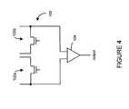
- FIG. 4illustrates a memory cell, in conjunction with a read amplifier, according to one embodiment of the present invention
- FIG. 5illustrates a memory cell including two transistors that are configured to have a common drain region, according to one embodiment of the present invention
- FIG. 6illustrates an exemplary layout of the memory cell of FIG. 5 ;
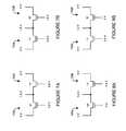
- FIGS. 7A, 7B , 8 A and 8 Billustrate writing and/or programming techniques including exemplary programming voltage values, according to two embodiments of the present invention, for the memory cell including two transistors that are configured to have a common drain region;
- FIG. 9illustrates a memory cell of this embodiment, in conjunction with a read amplifier and read operation including exemplary voltage values, according to an embodiment of the present invention, for the memory cell including two transistors that are configured to have a common drain region;
- FIGS. 10A and 10Billustrate writing and/or programming techniques including exemplary programming voltage values, according to two embodiments of the present invention, for a memory array including a plurality of memory cells each having two transistors that are configured to have a common drain region;
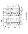
- FIG. 10Cillustrates exemplary read operation voltage values, according to an embodiment of the present invention, for a memory array including a plurality of memory cells each having two transistors that are configured to have a common drain region;
- FIG. 11illustrates a memory cell including two transistors that are configured to have a common source region and connected gates, according to one embodiment of the present invention
- FIG. 12illustrates an exemplary layout of the memory cell of FIG. 11 ;
- FIGS. 13A and 13Billustrate writing and/or programming techniques including exemplary programming voltage values, for the memory cell of FIG. 11 ;
- FIG. 14illustrates a memory cell of FIG. 11 , in conjunction with a read amplifier and read operation including exemplary voltage values, according to an embodiment of the present invention
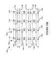
- FIGS. 15A and 15Billustrate writing and/or programming techniques including exemplary programming voltage values, for a memory array including a plurality of memory cells of FIG. 11 ;
- FIG. 15Cillustrates exemplary read operation voltage values, according to an embodiment of the present invention, for a memory array including a plurality of memory cells of FIG. 11 ;
- FIGS. 16A-16Cillustrate writing and/or programming techniques (including exemplary programming voltage values), according to another aspect of the present invention, for a memory cell of FIG. 11 ;
- FIGS. 17 and 18illustrate a memory array including a plurality of memory cells having a separate source line array that define a particular row of memory cells, and exemplary writing and/or programming techniques (including exemplary programming voltage values), according to another aspect of the present invention
- FIGS. 19A and 19Billustrate exemplary and alternative read operation voltage values, according to an embodiment of the present invention, for a memory array of FIGS. 17 and 18 ;
- FIG. 20illustrates an exemplary layout of the memory array of FIGS. 17 and 18 ;
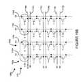
- FIGS. 21 and 22illustrate a memory array including a plurality of memory cells having a common source line array that define a particular row of memory cells, and exemplary writing and/or programming techniques (including exemplary programming voltage values), according to another aspect of the present invention
- FIG. 23illustrates exemplary read operation voltage values, according to an embodiment of the present invention, for a memory array of FIGS. 21 and 22 ;
- FIG. 24illustrates an exemplary layout of the memory array of FIGS. 21 and 22 ;
- FIGS. 25 and 26illustrate another memory array architecture including a plurality of memory cells having a common source line array, and exemplary writing and/or programming techniques (including exemplary programming voltage values), according to another aspect of the present invention
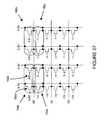
- FIG. 27illustrates exemplary read operation voltage values, according to an embodiment of the present invention, for a memory array of FIGS. 25 and 26 ;
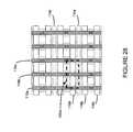
- FIG. 28illustrates an exemplary layout of the memory array of FIGS. 25 and 26 ;
- FIGS. 29 and 30illustrate a refresh architecture and technique for the memory cell and memory cell array according to one embodiment of the present invention.
- the present inventionis directed to a memory cell and technique of reading data from and writing data into that memory cell.
- the memory cellincludes two transistors which store complementary data states. That is, the two-transistor memory cell includes a first transistor that maintains a complementary state relative to the second transistor. As such, when programmed, one of the transistors of the memory cell stores a logic low (a binary “0”) and the other transistor of the memory cell stores a logic high (a binary “1”).
- the data state of the two-transistor complementary memory cellmay be read and/or determined by sampling, sensing measuring and/or detecting the polarity of the logic states stored in each transistor of complementary memory cell. That is, the two-transistor complementary memory cell is read by sampling, sensing, measuring and/or detecting the difference in signals (current or voltage) stored in the two transistors.
- memory cell 100is a bi-stable memory cell which includes transistor 102 a and transistor 102 b .
- transistor 102 astores a logic low and transistor 102 b stores a logic high.
- transistor 102 bstores a logic low.
- transistor 102 astores a logic high
- transistor 102 bstores a logic low.
- the state of memory cell 100may be read and/or determined by comparator 104 , which may be a voltage or current type comparator (for example, a cross-coupled sense amplifier).
- comparator 104may compare the different logic states stored in transistor 102 a and transistor 102 b .
- pass gates and/or column switch circuitrymay be employed to selectively connect transistors 102 a and 102 b to comparator 104 to facilitate the read operation of the data state of memory cell 100 .
- memory cell 100 of the present inventionmay include several advantages relative to conventional dynamic random access memory cells, including, for example: (i) the read operation is less sensitive to variation in the values of the binary states because a logic state is determined by the difference in states of the individual transistors, (ii) no reference circuit is necessary, (iii) the memory cell 100 includes a larger read window (as compared to conventional dynamic random access memory cells), which results in faster access time, and (iv) a less complicated and/or complex sense amplifier may be employed.
- the transistor 102 a and/or transistor 102 bmay be symmetrical or non-symmetrical devices. Where transistors 102 a and/or transistor 102 b are symmetrical, the source and drain regions are essentially interchangeable. However, where transistors 102 a and/or transistor 102 b are non-symmetrical devices, the source or drain regions of transistor 102 a and/or transistor 102 b may have different electrical, physical, doping concentration and/or doping profile characteristics. As such, the source or drain regions of the non-symmetrical device are typically not interchangeable.
- memory cell 100includes transistors 102 a and 102 b that have the same or similar characteristics.
- transistors 102 a and/or 102 bmay have the same or similar characteristics as the transistors described and illustrated in the Semiconductor Memory Device Patent Application.
- transistors 102 a and 102 bmay employ any type of design and/or control technique, whether now known or later developed, including, for example, those discussed above in the Semiconductor Memory Device Patent Application. All such designs of and/or control techniques for transistors 102 a and 102 b , whether now known or later developed, are intended to be within the present invention.
- transistors 102 a and 102 bare designed to have the same or similar characteristics, it may be advantageous to physically locate transistors 102 a and 102 b nearby each other. In this way, during manufacturing, transistors 102 a and 102 b are likely to be fabricated with little to no process variations or differences and, as such, transistors 102 a and 102 b are likely to have the same or similar electrical, physical, doping concentration and/or profile characteristics.
- a memory devicemay include a plurality of memory cells 100 arranged in repeating patterns.
- the memory cell 100may be arranged in an array in many different ways. All layout configurations for transistors 102 a and 102 b , whether now known or later developed, are intended to be within the present invention.
- transistors 102 a and 102 bare configured to have a common drain region.
- transistors 102 a and 102 binclude a common drain regions 110 a and 110 b .
- Datais written into or read from transistors 102 a and 102 b by applying suitable control signals to source regions 108 a and 108 b , drain regions 110 a and 110 b and/or gates 112 a and 112 b , respectively.
- charge carriersare accumulated in or emitted from electrically floating body regions 106 a and 106 b wherein the data state of each transistors 102 a and 102 b is defined by the amount of carriers within electrically floating body regions 106 a and 106 b , respectively.
- a logic low(binary “0” state) is written into transistor 102 a and a logic high (binary “1” state) is written into transistor 102 b using the indicated (exemplary) voltage levels.
- the voltage levels indicated in FIGS. 7A and 7Bmay be relative or absolute.
- a logic lowmay be written into transistor 102 a ( FIG. 7A ) or transistor 102 b ( FIG. 7B ) using the voltages indicated.
- the voltages indicatedmay be relative in that each voltage level, for example, may be increased or decreased by a given voltage (for example, 0.5 volts).
- the logic levelsmay be programmed into transistors 102 a and 102 b using a low power consumption technique.
- the low power consumption techniqueemploys positive and negative control signals/voltages in order to program the complementary states. For example, a logic high is written into transistor 102 a ( FIG. 8B ) and a logic high is written into transistor 102 b ( FIG. 8A ) using a negative gate voltage.
- the source regions 108 a and 108 b of transistors 102 a and 102 bare employed to read, sense and/or determine the data state of cell 100 .
- source regions 108 a and 108 bare selectively connected to comparator 104 (for example, a voltage or current sense amplifier) to permit the logic value of memory cell 110 to be read, sensed and/or determined.
- comparator 104for example, a voltage or current sense amplifier
- transistors 102 a and 102 bmay store the respective data state via majority carriers within the electrically floating body regions 106 a and 106 b , respectively.
- the logic state of each transistor 102 a and 102 bis read by comparator 104 in a differential manner. Exemplary read voltage signals are indicated in FIG. 9 .
- a memory devicemay include a plurality of memory cells 100 , arranged in repeating patterns.
- the exemplary write techniquesdescribed above, are illustrated in a schematic representation of a memory matrix.
- the exemplary read techniquedescribed above, is illustrated in a schematic representation of a memory matrix.
- 10A-10Cmay reduce, minimize and/or eliminate any disturbance issues (for example, issues of stored charge loss or gain within memory cells) caused to memory cells having common gate lines, drain lines and/or source lines with memory cells that are accessed via read and write operations.
- disturbance issuesfor example, issues of stored charge loss or gain within memory cells
- memory cell 100may include a layout whereby transistors 102 a and 102 b include (1) common source regions 108 a and 108 b , respectively, and (2) gates 112 a and 112 b , respectively, that are connected to the same gate line 118 .
- Exemplary write techniquesare indicated in FIG. 13A (write logic low) and FIG. 13B (write logic high).
- An exemplary read techniqueis illustrated in FIG. 14 .
- the voltage levels indicated in FIGS. 13A, 13B and 14may be relative or absolute.
- a logic lowmay be written into transistor 102 a ( FIG. 13A ) or transistor 102 b ( FIG. 13B ) using the voltages indicated.
- the voltages indicatedmay be relative in that each voltage level, for example, may be increased or decreased by a given voltage (for example, 0.25 volts).
- a memory array having a plurality of memory cells 100 wherein the source regions and gates (gate lines) of transistors 102 a and 102 b are in commonmay include a layout as illustrated in FIGS. 15A-15C .
- exemplary write techniques of the memory array of this embodimentare illustrated in a schematic representation of a memory matrix.
- an exemplary read techniqueis illustrated in a schematic representation of a memory matrix including a plurality of memory cells 100 configured with common source regions and gates (gate line).
- the exemplary read and write techniques of FIGS. 15A-15Cincluding the exemplary levels of the read and write voltages, may reduce, minimize and/or eliminate any disturbance issues (to neighboring cells) that may result using other read and write voltage levels.
- a two-step write operationmay be employed to program memory cell 100 a with little to no disturbance to adjacent and/or neighboring cells (i.e., cells that share source lines, drain lines and/or gate lines).
- an entire row of memory cellsmay first be written to the same logic state and thereafter, individual bits are written to the opposite state in accordance with a desired data state (i.e., the individual bits are written to another state to reflect a desired data state).
- the memory cells having a common source lineare first written to the same logic state (for example, logic high or binary “1”). In this way, the state of memory cell 100 is “cleared”. Thereafter, individual transistors 102 of memory cells 100 are written to a particular, desired and/or predetermined logic state (see, for example, FIG. 16B (write “0”) and FIG. 16C (write “1”)) according to the particular, desired and/or predetermined logic state of memory cell 100 . That is, one of the transistors of memory cell 100 is written to logic low (binary “0”) to write either a logic high or logic low into memory cell 100 (i.e., transistor 102 a of FIG. 16B to store logic low in memory cell 100 ; and transistor 102 b of FIG. 16C to store logic high in memory cell 100 ). Notably, writing logic low to the other transistor of memory cell 100 is inhibited by applying a suitable bitline voltage.
- the first step of the write operationclears the memory cells having a common source line and the second step writes or stores new data or the previous data (in the event that the data did not change).
- Array architectures employing this write operation techniquemay have an advantage that the memory cells of the array are not “disturbed” (or experience little and/or negligible disturbance) because “high” voltages are applied in the row direction (i.e., on source lines 114 ) but not in the column direction (i.e., on the drain lines 116 ).
- this write techniquemay be performed as a page mode write where the page is first “cleared” and then individual bytes (or bits) in a page are written to a new state.
- Such a write techniquemay also be suitable for other memory array architectures or configurations.
- the write techniquemay be implemented where memory cells 100 of each row of transistors 102 has a dedicated source line to minimize, reduce and/or eliminate disturbance on adjacent rows.
- a given rowmay be written to by applying a clear operation followed by a selective write operation.
- a plurality of memory cells 100having gates that are connected to a common gate line, are arranged to form row 120 .
- Exemplary voltages that implement a clear operation for row 120 and maintain the remaining portion of the array in a fixed state (i.e., unchanged in response to the clear operation)are indicated in FIG. 17 .
- the same logic statefor example, logic high or binary “1” is stored in both transistors 102 a and 102 b of memory cells 100 of row 120 . In this way, the state of memory cell 100 is “cleared”.
- individual transistors 102 a and 102 b of the memory cells 100 of row 120are written to a particular, desired and/or predetermined logic state (see, for example, FIG. 18 (write “1”) in memory cell 100 a ) in order to store a particular, desired and/or predetermined logic state in memory cell 100 . That is, as described above, one of the transistors of memory cell 100 is written to logic low (binary “0”) to write either a logic high or logic low into memory cell 100 . Notably, writing logic low to the other transistor of the memory cell 100 is inhibited by applying a suitable bitline voltage.
- the datamay be read from memory cells 100 of row 120 by applying the exemplary voltages indicated.
- the exemplary read voltages of FIG. 19Bmay avoid, reduce and/or minimize the need for charge pumping to eliminate minority carriers from the floating body—gate interface.
- FIGS. 21-24Another memory array architectures that may employ the two-step write technique that eliminates, minimizes and/or reduces disturbance to memory cells when reading from and/or writing to adjacent memory cells is illustrated in FIGS. 21-24 .
- the source linesare shared but bit lines are separated.
- the transistors 102 a and 102 b of memory cell 100 aare located on separate rows.
- the gates of transistors 102 a and 102 bare connected together at the array boundary.
- transistors 102 a and 102 b of memory cell 100 aare located on separate rows with the gates of each transistor 102 a and 102 b connected at, for example, the array boundary.
- FIGS. 25-28illustrate another memory array architecture in which a plurality of memory cells “share” a source line and employ the two-step write technique that may eliminate, minimize and/or reduce disturbance to memory cells when reading from and/or writing to adjacent memory cells.
- a given rowmay be written to by applying suitable voltages to implement a clear operation followed by a selective write operation.
- a write inhibit signalis applied to the gates of memory cells that share a source line 114 (for example, a write inhibit signal may be applied to the gates of transistors that comprise memory cell 100 x and memory cell 100 y ).
- exemplary voltages that implement a clear operation for row 120 and maintain the neighboring memory cells (for example, memory cells 100 x and 100 y ) remaining portion of the array in a fixed state (i.e., unchanged in response to the clear operation)are indicated in FIG. 25 .
- the individual transistors 102 of the memory cells 100 of row 120are written to a particular, desired and/or predetermined logic state (see, for example, FIG. 26 (write “1”) in memory cell 100 a ) in order to store a particular, desired and/or predetermined logic state of the memory cell 100 . That is, as described above, one of the transistors of memory cell 100 is written to logic low (binary “0”) to write either a logic high or logic low into the memory cell 100 .
- the datamay be read from memory cells 100 of row 120 by applying the exemplary voltages indicated.
- an exemplary read inhibit voltage for the remaining portion of the array (including the neighboring memory cells)is also indicated.
- the read inhibit voltage/signalmaintains the unselected portion of the array in a fixed state (i.e., unchanged in response to the read operation).
- the memory cell 100is a dynamic storage device. As such, memory cell 100 must be periodically or intermittently refreshed to maintain its data state.
- FIGS. 29 and 30illustrate an exemplary (and inventive) refresh configuration and technique for refreshing and/or re-storing the data state of memory cell 100 .
- gates 112 a and 112 b and source regions 108 a and 108 b of transistors 102 a and 102 b (respectively) of memory cell 100are connected and thereafter a current (I) is applied on the electrically shorted gates and sources.
- the drain regions 110 a and 110 b of transistors 102 a and 102 bare maintained at a predetermined voltage (for example, 0V).
- the forced current (I)will pass mainly through the transistor having the lower threshold (i.e., the transistor storing a logic high (binary “1”)).
- the transistor currentswill differ by orders of magnitude.
- the higher current through the low threshold transistorwill inject holes into the body of that transistor and, as such, will reinforce the logic high (binary “1”).
- the high threshold transistormay have some hole injection but not enough to overcome the natural tendency to return to the neutral state.
- the current (I)may also be applied to the electrically shorted gates and drains with the sources maintained at a predetermined voltage (for example, 0V).
- FIG. 30illustrates the refresh technique in the context of a memory array wherein row 120 of memory cells 100 are refreshed.
- the forced currentflows almost exclusively through all the transistors storing a logic high (binary “1”).
- this refresh techniqueis well suited to the memory cells and memory array architecture of the present inventions because the optimum range of forced current is independent of the data stored in the refreshed row (that is, half the transistors contain a logic high and the other half contain a logic low).
- FIG. 30illustrates a “separated source” array architecture
- the techniqueis also applicable to the other array architectures described herein.
- the discussion regarding refreshwill not be repeated for such other array architectures.
- the illustrated voltage levels to implement the write and read operationsare exemplary.
- the indicated voltage levelsmay be relative or absolute. That is, for example, a logic low may be written into transistor 102 a (see, for example, FIG. 7A ) or transistor 102 b (see, for example, FIG. 7B ) using the voltages indicated therein.
- the voltages indicatedmay be relative in that each voltage level, for example, may be increased or decreased by a given voltage amount (for example, each voltage may be increased by 0.5 volts).
- the inventions(and embodiments thereof described herein are entirely applicable to P-channel transistors.
- majority carriers in body region 18are electrons and minority carriers are holes.
- the memory arraysmay be comprised of N-channel, P-channel and/or both types of transistors.
- the circuitry that is peripheral to the memory arraymay include P-channel and/or N-channel type transistors, including transistors like transistor 14 .
- memory cell(s) 102may also employ the structure, features, attributes, architectures, configurations, materials, techniques and advantages described and illustrated in non-provisional patent application entitled “Semiconductor Device”, which was filed on Feb. 18, 2004, by Fazan and Okhonin, and assigned Ser. No. 10/487,157 (hereinafter “Semiconductor Device Patent Application”).
- semiconductor Device Patent ApplicationThe entire contents of the Semiconductor Device Patent Application, including, for example, the inventions, features, attributes, architectures, configurations, materials, techniques and advantages described and illustrated therein, are hereby incorporated by reference herein.
Landscapes
- Engineering & Computer Science (AREA)
- Microelectronics & Electronic Packaging (AREA)
- Computer Hardware Design (AREA)
- Semiconductor Memories (AREA)
- Dram (AREA)
- For Increasing The Reliability Of Semiconductor Memories (AREA)
Abstract
Description
- This application claims priority to: U.S. Provisional Application Ser. No. 60/470,385, entitled “Two Transistor Gain Cell”, filed May 13, 2003 (hereinafter “the Provisional Application”). The contents of the Provisional Application are incorporated by reference herein in their entirety.
- This invention relates to a semiconductor memory cell, array, architecture and device, and techniques for controlling and/or operating such cell and device; and more particularly, in one aspect, to a semiconductor dynamic random access memory (“DRAM”) cell, array, architecture and/or device wherein the memory cell includes an electrically floating body in which an electrical charge is stored.
- There are many different types and/or forms of DRAM cells, including, for example, a semiconductor memory cell consisting of an access transistor and a capacitor, which stores an electric charge representing a bi-stable memory state. The access transistor serves as a switch for controlling the charging and discharging of the capacitor as well as reading and writing of the logic states into the capacitor (i.e., charging or discharging the capacitor).
- Although significant integration densities can be achieved with DRAM devices employing one transistor—one capacitor memory cells, such devices tend to be limited or restricted with respect to the size of the memory cell. In this regard, conventional techniques employ stacked and/or trench capacitor approaches, whereby the capacitor is partially disposed above and/or below an access transistor.
- In addition, DRAM devices employing one transistor—one capacitor memory cells tend to be fabricated using manufacturing processes that are different from and/or incompatible with manufacturing processes for logic devices (for example, microprocessors). As a result, integration of one transistor—one capacitor memory cells into logic devices is often complicated and expensive.
- Another type of dynamic random access memory cell is described and illustrated in non-provisional patent application entitled “Semiconductor Memory Device”, which was filed on Jun. 10, 2003 and assigned Ser. No. 10/450,238 (hereinafter “Semiconductor Memory Device Patent Application”). With reference to
FIGS. 1A and 1B , the Semiconductor Memory Device Patent Application discloses, among other things,semiconductor DRAM device 10 in which eachmemory cell 12 consists oftransistor 14 havinggate 16,body region 18, which is electrically floating,source region 20 anddrain region 22. Thebody region 18 is disposed between and adjacent tosource region 20 and drainregion 22. Data is written into or read from a selected memory cell by applying suitable control signals to a selected word line(s)24, a selected source line(s)26 and/or a selected bit line(s)28. In response, charge carriers are accumulated in or emitted and/or ejected from electrically floatingbody region 18 wherein the data states are defined by the amount of carriers within electrically floatingbody region 18. Notably, the entire contents of the Semiconductor Memory Device Patent Application, including, for example, the features, attributes, architectures, configurations, materials, techniques and advantages described and illustrated therein, are incorporated by reference herein. - In particular, in one embodiment, the memory cell of the Semiconductor Memory Device Patent Application operates by accumulating in or emitting/ejecting majority carriers (electrons or holes)30 from
body region 18 of, for example, N-channel transistors. (See,FIGS. 2A and 2B ). In this regard, accumulating majority carriers (in this example, “holes”)30 inbody region 18 ofmemory cells 12 via, for example, impact ionization nearsource region 20 and/ordrain region 22, is representative of a logic high or “1” data state. (See,FIG. 2A ). Emitting or ejectingmajority carriers 30 frombody region 18 via, for example, forward biasing the source/body junction and/or the drain/body junction, is representative of a logic low or “0”. (See,FIG. 2B ). - Several techniques may be implemented to read the data stored in (or write the data into) a memory device of the Semiconductor Memory Device Patent Application. For example, a current sense amplifier (not illustrated) may be employed to read the data stored in
memory cells 12. In this regard, a current sense amplifier may compare the cell current to a reference current, for example, the current of a reference cell (not illustrated). From that comparison, it may be determined whethermemory cell 12 contained a logic high (relatively more majority carries30 contained within body region18) or logic low data state (relatively less majority carries28 contained within body region18). - Notably,
transistor 14 may be a symmetrical or non-symmetrical device. Wheretransistor 14 is symmetrical, the source and drain regions are essentially interchangeable. However, wheretransistor 14 is a non-symmetrical device, the source or drain regions oftransistor 14 have different electrical, physical, doping concentration and/or doping profile characteristics. As such, the source or drain regions of a non-symmetrical device are typically not interchangeable. - There are many inventions described and illustrated herein. In a first principal aspect, the present invention is a semiconductor dynamic random access memory cell for storing a first data state and a second data state. The memory cell includes first and second transistors, wherein each transistor includes a source region, a drain region, an electrically floating body region disposed between and adjacent to the source region and the drain region, and a gate spaced apart from, and capacitively coupled to, the body region. In addition, each transistor includes a first state representative of a first charge in the body region, and a second data state representative of a second charge in the body region. Further the memory cell is in: (1) the first data state when the first transistor is in the first state and the second transistor is in the second state and (2) the second data state when the first transistor is in the second state and the second transistor is in the first state.
- In one embodiment, the semiconductor dynamic random access memory cell includes two outputs including a first output connected to the drain region of the first transistor and a second output connected to the drain region of the second transistor. In this embodiment, the gate of the first transistor is connected to the gate of the second transistor, and the source region of the first transistor and the source region of the second transistor are the same region.
- In another embodiment, the semiconductor dynamic random access memory cell includes two outputs including a first output connected to the source region of the first transistor and a second output connected to the source region of the second transistor. In this embodiment, the drain region of the first transistor and the drain region of the second transistor are the same region.
- Notably, the memory cell may be programmed to a first data state by applying a first control signal to the gate of the first transistor and a second control signal to the gate of the second transistor and wherein the first and second control signals include different voltage amplitudes.
- In another principal aspect, the present invention is a semiconductor memory array comprising a plurality of semiconductor dynamic random access memory cells arranged in a matrix of rows and columns. Each semiconductor dynamic random access memory cell includes first and second transistors. Each transistor includes a source region, a drain region, a electrically floating body region disposed between and adjacent to the source region and the drain region, and a gate spaced apart from, and capacitively coupled to, the body region. The transistors include a first state representative of a first charge in the body region; and a second data state representative of a second charge in the body region. Further each memory cell is in: (1) the first data state when its first transistor is in the first state and its second transistor is in the second state and (2) the second data state when its first transistor is in the second state and its second transistor is in the first state.
- The semiconductor memory array may also include a comparator having a plurality of inputs to sense the states of the first and second transistors of a semiconductor dynamic random access memory cell of the plurality of semiconductor dynamic random access memory cell. A first input of the comparator is selectively coupled to a first transistor of the semiconductor dynamic random access memory cell and the second input of the comparator is selectively coupled to the second transistor of a semiconductor dynamic random access memory cell.
- In one embodiment, at least one of the rows of semiconductor dynamic random access memory cells includes a source line that is connected to each of the semiconductor dynamic random access memory cells of the row. Indeed, in another embodiment, each row of semiconductor dynamic random access memory cells includes an associated source line which is connected to only the semiconductor dynamic random access memory cells of the associated row.
- In another embodiment, a first input of a comparator is selectively coupled to the drain region of the first transistor of the semiconductor dynamic random access memory cell and a second input of the comparator is selectively coupled to the drain of second first transistor of a semiconductor dynamic random access memory cell. In this embodiment, each row of semiconductor dynamic random access memory cells includes an associated source line which is connected to only the semiconductor dynamic random access memory cells of the row.
- The semiconductor dynamic random access memory cell may be programmed in a first data state by performing a clear operation of the first and second transistors of the semiconductor dynamic random access memory cell and then performing a write operation. In response, the first transistor of the semiconductor dynamic random access memory cell is in a first state and the second transistor of the semiconductor dynamic random access memory cell is in a second state.
- Moreover, the semiconductor dynamic random access memory cell may be programmed in a first data state by first placing the first and second transistors of the semiconductor dynamic random access memory cell in a first state and thereafter placing the second transistor of the semiconductor dynamic random access memory cell is in a second state. In this embodiment, an unselected portion of the semiconductor memory array is maintained in a fixed state when programming the at least one semiconductor dynamic random access memory cell by applying a write inhibit signal to the transistors of the semiconductor dynamic random access memory cells comprising the unselected portion of the semiconductor memory array.
- In one embodiment, each semiconductor dynamic random access memory cell includes two outputs including a first output connected to the drain region of the first transistor and a second output connected to the drain region of the second transistor.
- In another embodiment, the gate of the first transistor and the gate of the second transistor of each semiconductor dynamic random access memory cell are each connected to an associated common gate line.
- In yet another embodiment, the source region of the first transistor and the source region of the second transistor of each semiconductor dynamic random access memory cell are the same region. However, in another embodiment, the source region of the first transistor and the source region of the second transistor of each semiconductor dynamic random access memory cell are connected to different source lines.
- Indeed, a first output of each semiconductor dynamic random access memory cell may be connected to the source region of the first transistor and a second output of the semiconductor dynamic random access memory cell may be connected to the source region of the second transistor. In this embodiment, the drain region of the first transistor and the drain region of the second transistor of each semiconductor dynamic random access memory cell are the same region.
- Again, there are many inventions described and illustrated herein. This Summary of the Invention is not exhaustive of the scope of the present invention. Moreover, this Summary is not intended to be limiting of the invention and should not be interpreted in that manner. While certain embodiments, features, attributes and advantages of the inventions have been described in this Summary, it should be understood that many others, as well as different and/or similar embodiments, features, attributes and/or advantages of the present inventions, which are apparent from the description, illustrations and claims, which follow.
- In the course of the detailed description to follow, reference will be made to the attached drawings. These drawings show different aspects of the present invention and, where appropriate, reference numerals illustrating like structures, components, materials and/or elements in different figures are labeled similarly. It is understood that various combinations of the structures, components, materials and/or elements, other than those specifically shown, are contemplated and are within the scope of the present invention.
FIG. 1A is a schematic representation of a semiconductor DRAM array as illustrated (and described) in the Semiconductor Memory Device Patent Application;FIG. 1B illustrates a memory cell according to the Semiconductor Memory Device Patent Application;FIGS. 2A and 2B are exemplary schematic illustrations of the charge relationship, for a particular memory state, of the floating body, source and drain regions of a memory cell according to the Semiconductor Memory Device Patent Application;FIGS. 3A and 3B illustrate a memory cell, according to certain embodiments of certain aspects of the present inventions;FIG. 4 illustrates a memory cell, in conjunction with a read amplifier, according to one embodiment of the present invention;FIG. 5 illustrates a memory cell including two transistors that are configured to have a common drain region, according to one embodiment of the present invention;FIG. 6 illustrates an exemplary layout of the memory cell ofFIG. 5 ;FIGS. 7A, 7B ,8A and8B illustrate writing and/or programming techniques including exemplary programming voltage values, according to two embodiments of the present invention, for the memory cell including two transistors that are configured to have a common drain region;FIG. 9 illustrates a memory cell of this embodiment, in conjunction with a read amplifier and read operation including exemplary voltage values, according to an embodiment of the present invention, for the memory cell including two transistors that are configured to have a common drain region;FIGS. 10A and 10B illustrate writing and/or programming techniques including exemplary programming voltage values, according to two embodiments of the present invention, for a memory array including a plurality of memory cells each having two transistors that are configured to have a common drain region;FIG. 10C illustrates exemplary read operation voltage values, according to an embodiment of the present invention, for a memory array including a plurality of memory cells each having two transistors that are configured to have a common drain region;FIG. 11 illustrates a memory cell including two transistors that are configured to have a common source region and connected gates, according to one embodiment of the present invention;FIG. 12 illustrates an exemplary layout of the memory cell ofFIG. 11 ;FIGS. 13A and 13B illustrate writing and/or programming techniques including exemplary programming voltage values, for the memory cell ofFIG. 11 ;FIG. 14 illustrates a memory cell ofFIG. 11 , in conjunction with a read amplifier and read operation including exemplary voltage values, according to an embodiment of the present invention;FIGS. 15A and 15B illustrate writing and/or programming techniques including exemplary programming voltage values, for a memory array including a plurality of memory cells ofFIG. 11 ;FIG. 15C illustrates exemplary read operation voltage values, according to an embodiment of the present invention, for a memory array including a plurality of memory cells ofFIG. 11 ;FIGS. 16A-16C illustrate writing and/or programming techniques (including exemplary programming voltage values), according to another aspect of the present invention, for a memory cell ofFIG. 11 ;FIGS. 17 and 18 illustrate a memory array including a plurality of memory cells having a separate source line array that define a particular row of memory cells, and exemplary writing and/or programming techniques (including exemplary programming voltage values), according to another aspect of the present invention;FIGS. 19A and 19B illustrate exemplary and alternative read operation voltage values, according to an embodiment of the present invention, for a memory array ofFIGS. 17 and 18 ;FIG. 20 illustrates an exemplary layout of the memory array ofFIGS. 17 and 18 ;FIGS. 21 and 22 illustrate a memory array including a plurality of memory cells having a common source line array that define a particular row of memory cells, and exemplary writing and/or programming techniques (including exemplary programming voltage values), according to another aspect of the present invention;FIG. 23 illustrates exemplary read operation voltage values, according to an embodiment of the present invention, for a memory array ofFIGS. 21 and 22 ;FIG. 24 illustrates an exemplary layout of the memory array ofFIGS. 21 and 22 ;FIGS. 25 and 26 illustrate another memory array architecture including a plurality of memory cells having a common source line array, and exemplary writing and/or programming techniques (including exemplary programming voltage values), according to another aspect of the present invention;FIG. 27 illustrates exemplary read operation voltage values, according to an embodiment of the present invention, for a memory array ofFIGS. 25 and 26 ;FIG. 28 illustrates an exemplary layout of the memory array ofFIGS. 25 and 26 ; andFIGS. 29 and 30 illustrate a refresh architecture and technique for the memory cell and memory cell array according to one embodiment of the present invention.- There are many inventions described and illustrated herein. In a first aspect, the present invention is directed to a memory cell and technique of reading data from and writing data into that memory cell. In this regard, in one embodiment of this aspect of the invention, the memory cell includes two transistors which store complementary data states. That is, the two-transistor memory cell includes a first transistor that maintains a complementary state relative to the second transistor. As such, when programmed, one of the transistors of the memory cell stores a logic low (a binary “0”) and the other transistor of the memory cell stores a logic high (a binary “1”).
- The data state of the two-transistor complementary memory cell may be read and/or determined by sampling, sensing measuring and/or detecting the polarity of the logic states stored in each transistor of complementary memory cell. That is, the two-transistor complementary memory cell is read by sampling, sensing, measuring and/or detecting the difference in signals (current or voltage) stored in the two transistors.
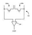
- With reference to
FIGS. 3A and 3B , in one embodiment,memory cell 100 is a bi-stable memory cell which includestransistor 102aandtransistor 102b. In a first logic state ofmemory cell 100,transistor 102astores a logic low andtransistor 102bstores a logic high. (See, for example,FIG. 3A ). In contrast, in a second logic state ofmemory cell 100,transistor 102astores a logic high andtransistor 102bstores a logic low. (See, for example,FIG. 3B ). - With reference to
FIG. 4 , the state ofmemory cell 100 may be read and/or determined bycomparator 104, which may be a voltage or current type comparator (for example, a cross-coupled sense amplifier). In this regard,comparator 104 may compare the different logic states stored intransistor 102aandtransistor 102b. Thus, wheretransistor 102aandtransistor 102bstore either logic “1” or logic “0”, the difference is either 1−0=1 or 0−1=−1. As such, the read window may be described as the absolute difference between the logic high state and logic low state (i.e., 1−(−1)=2), which may be 2× the read window of the conventional memory cell. Notably, pass gates and/or column switch circuitry (not illustrated) may be employed to selectively connecttransistors comparator 104 to facilitate the read operation of the data state ofmemory cell 100. - Thus,
memory cell 100 of the present invention may include several advantages relative to conventional dynamic random access memory cells, including, for example: (i) the read operation is less sensitive to variation in the values of the binary states because a logic state is determined by the difference in states of the individual transistors, (ii) no reference circuit is necessary, (iii) thememory cell 100 includes a larger read window (as compared to conventional dynamic random access memory cells), which results in faster access time, and (iv) a less complicated and/or complex sense amplifier may be employed. - The
transistor 102aand/ortransistor 102bmay be symmetrical or non-symmetrical devices. Wheretransistors 102aand/ortransistor 102bare symmetrical, the source and drain regions are essentially interchangeable. However, wheretransistors 102aand/ortransistor 102bare non-symmetrical devices, the source or drain regions oftransistor 102aand/ortransistor 102bmay have different electrical, physical, doping concentration and/or doping profile characteristics. As such, the source or drain regions of the non-symmetrical device are typically not interchangeable. - In one embodiment,
memory cell 100 includestransistors transistors 102aand/or102bmay have the same or similar characteristics as the transistors described and illustrated in the Semiconductor Memory Device Patent Application. Notably,transistors transistors - In those instances where
transistors transistors transistors transistors - A memory device may include a plurality of
memory cells 100 arranged in repeating patterns. Thememory cell 100 may be arranged in an array in many different ways. All layout configurations fortransistors transistors FIGS. 5 and 6 , in one embodiment,transistors common drain regions transistors regions drain regions gates body regions transistors body regions - In particular, with reference to
FIGS. 7A and 7B , in one embodiment, a logic low (binary “0” state) is written intotransistor 102aand a logic high (binary “1” state) is written intotransistor 102busing the indicated (exemplary) voltage levels. Notably, the voltage levels indicated inFIGS. 7A and 7B may be relative or absolute. In this regard, a logic low may be written intotransistor 102a(FIG. 7A ) ortransistor 102b(FIG. 7B ) using the voltages indicated. Alternatively, the voltages indicated may be relative in that each voltage level, for example, may be increased or decreased by a given voltage (for example, 0.5 volts). - With reference to
FIGS. 8A and 8B , the logic levels may be programmed intotransistors transistor 102a(FIG. 8B ) and a logic high is written intotransistor 102b(FIG. 8A ) using a negative gate voltage. - The
source regions transistors cell 100. In this regard,source regions transistors body regions transistor comparator 104 in a differential manner. Exemplary read voltage signals are indicated inFIG. 9 . - Notably, pass gates and/or column switch circuitry (not illustrated) may be employed to selectively connect
source regions transistors cell 100. Moreover, as is apparent fromFIG. 6 , a memory device may include a plurality ofmemory cells 100, arranged in repeating patterns. In this regard, with reference toFIGS. 10A and 10B , the exemplary write techniques, described above, are illustrated in a schematic representation of a memory matrix. Further, with reference toFIG. 10C , the exemplary read technique, described above, is illustrated in a schematic representation of a memory matrix. Notably, the exemplary read and write techniques ofFIGS. 10A-10C , including the exemplary levels of the read and write voltages, may reduce, minimize and/or eliminate any disturbance issues (for example, issues of stored charge loss or gain within memory cells) caused to memory cells having common gate lines, drain lines and/or source lines with memory cells that are accessed via read and write operations. - In another embodiment, with reference to
FIGS. 11 and 12 ,memory cell 100 may include a layout wherebytransistors common source regions gates FIG. 13A (write logic low) andFIG. 13B (write logic high). An exemplary read technique is illustrated inFIG. 14 . Notably, the voltage levels indicated inFIGS. 13A, 13B and14 may be relative or absolute. In this regard, a logic low may be written intotransistor 102a(FIG. 13A ) ortransistor 102b(FIG. 13B ) using the voltages indicated. Alternatively, the voltages indicated may be relative in that each voltage level, for example, may be increased or decreased by a given voltage (for example, 0.25 volts). - A memory array having a plurality of
memory cells 100 wherein the source regions and gates (gate lines) oftransistors FIGS. 15A-15C . In this regard, with reference toFIGS. 15A and 15B , exemplary write techniques of the memory array of this embodiment are illustrated in a schematic representation of a memory matrix. With reference toFIG. 15C , an exemplary read technique is illustrated in a schematic representation of a memory matrix including a plurality ofmemory cells 100 configured with common source regions and gates (gate line). Notably, the exemplary read and write techniques ofFIGS. 15A-15C , including the exemplary levels of the read and write voltages, may reduce, minimize and/or eliminate any disturbance issues (to neighboring cells) that may result using other read and write voltage levels. - In certain embodiments, it may be advantageous to further reduce, minimize and/or eliminate any issues of disturbance (for example, issues of stored charge loss or gain within memory cells) of the data states of memory cells having common gate lines, drain lines and/or source lines with those memory cells that are being accessed (i.e., being read from or written to). In one embodiment, a two-step write operation may be employed to
program memory cell 100awith little to no disturbance to adjacent and/or neighboring cells (i.e., cells that share source lines, drain lines and/or gate lines). In this regard, an entire row of memory cells may first be written to the same logic state and thereafter, individual bits are written to the opposite state in accordance with a desired data state (i.e., the individual bits are written to another state to reflect a desired data state). - In particular, with reference to
FIG. 16A , in one embodiment, the memory cells having a common source line are first written to the same logic state (for example, logic high or binary “1”). In this way, the state ofmemory cell 100 is “cleared”. Thereafter, individual transistors102 ofmemory cells 100 are written to a particular, desired and/or predetermined logic state (see, for example,FIG. 16B (write “0”) andFIG. 16C (write “1”)) according to the particular, desired and/or predetermined logic state ofmemory cell 100. That is, one of the transistors ofmemory cell 100 is written to logic low (binary “0”) to write either a logic high or logic low into memory cell100 (i.e.,transistor 102aofFIG. 16B to store logic low inmemory cell 100; andtransistor 102bofFIG. 16C to store logic high in memory cell100). Notably, writing logic low to the other transistor ofmemory cell 100 is inhibited by applying a suitable bitline voltage. - Thus, in this embodiment, the first step of the write operation clears the memory cells having a common source line and the second step writes or stores new data or the previous data (in the event that the data did not change). Array architectures employing this write operation technique may have an advantage that the memory cells of the array are not “disturbed” (or experience little and/or negligible disturbance) because “high” voltages are applied in the row direction (i.e., on source lines114) but not in the column direction (i.e., on the drain lines116). Notably, this write technique may be performed as a page mode write where the page is first “cleared” and then individual bytes (or bits) in a page are written to a new state.
- Such a write technique may also be suitable for other memory array architectures or configurations. For example, the write technique may be implemented where
memory cells 100 of each row of transistors102 has a dedicated source line to minimize, reduce and/or eliminate disturbance on adjacent rows. With reference toFIGS. 17, 18 ,19A and19B, and20, in one embodiment, a given row may be written to by applying a clear operation followed by a selective write operation. In this regard, a plurality ofmemory cells 100, having gates that are connected to a common gate line, are arranged to formrow 120. Exemplary voltages that implement a clear operation forrow 120 and maintain the remaining portion of the array in a fixed state (i.e., unchanged in response to the clear operation) are indicated inFIG. 17 . In response, the same logic state (for example, logic high or binary “1”) is stored in bothtransistors memory cells 100 ofrow 120. In this way, the state ofmemory cell 100 is “cleared”. - Thereafter,
individual transistors memory cells 100 ofrow 120 are written to a particular, desired and/or predetermined logic state (see, for example,FIG. 18 (write “1”) inmemory cell 100a) in order to store a particular, desired and/or predetermined logic state inmemory cell 100. That is, as described above, one of the transistors ofmemory cell 100 is written to logic low (binary “0”) to write either a logic high or logic low intomemory cell 100. Notably, writing logic low to the other transistor of thememory cell 100 is inhibited by applying a suitable bitline voltage. - With reference to
FIGS. 19A and 19B , the data may be read frommemory cells 100 ofrow 120 by applying the exemplary voltages indicated. Notably, the exemplary read voltages ofFIG. 19B may avoid, reduce and/or minimize the need for charge pumping to eliminate minority carriers from the floating body—gate interface. - Another memory array architectures that may employ the two-step write technique that eliminates, minimizes and/or reduces disturbance to memory cells when reading from and/or writing to adjacent memory cells is illustrated in
FIGS. 21-24 . In this architecture, the source lines are shared but bit lines are separated. Thetransistors memory cell 100aare located on separate rows. The gates oftransistors - Notably,
transistors memory cell 100aare located on separate rows with the gates of eachtransistor drain lines transistor memory cell 100aso that eachtransistor FIG. 23 ). FIGS. 25-28 illustrate another memory array architecture in which a plurality of memory cells “share” a source line and employ the two-step write technique that may eliminate, minimize and/or reduce disturbance to memory cells when reading from and/or writing to adjacent memory cells. In this regard, with reference toFIGS. 25 and 26 , in one embodiment, a given row may be written to by applying suitable voltages to implement a clear operation followed by a selective write operation. In conjunction with applying suitable voltages to implement the clear operation, a write inhibit signal is applied to the gates of memory cells that share a source line114 (for example, a write inhibit signal may be applied to the gates of transistors that comprisememory cell 100xandmemory cell 100y).- In particular, exemplary voltages that implement a clear operation for
row 120 and maintain the neighboring memory cells (for example,memory cells FIG. 25 . The individual transistors102 of thememory cells 100 ofrow 120 are written to a particular, desired and/or predetermined logic state (see, for example,FIG. 26 (write “1”) inmemory cell 100a) in order to store a particular, desired and/or predetermined logic state of thememory cell 100. That is, as described above, one of the transistors ofmemory cell 100 is written to logic low (binary “0”) to write either a logic high or logic low into thememory cell 100. - With reference to
FIG. 27 , the data may be read frommemory cells 100 ofrow 120 by applying the exemplary voltages indicated. Notably, an exemplary read inhibit voltage for the remaining portion of the array (including the neighboring memory cells) is also indicated. The read inhibit voltage/signal maintains the unselected portion of the array in a fixed state (i.e., unchanged in response to the read operation). - The
memory cell 100 is a dynamic storage device. As such,memory cell 100 must be periodically or intermittently refreshed to maintain its data state.FIGS. 29 and 30 illustrate an exemplary (and inventive) refresh configuration and technique for refreshing and/or re-storing the data state ofmemory cell 100. In one embodiment,gates source regions transistors memory cell 100 are connected and thereafter a current (I) is applied on the electrically shorted gates and sources. Thedrain regions transistors - With reference to
FIG. 29 , in operation, becausetransistors memory cell 100 have different thresholds depending on which transistor is storing logic low and which transistor is storing a logic high, the forced current (I) will pass mainly through the transistor having the lower threshold (i.e., the transistor storing a logic high (binary “1”)). With a small forced current, the transistor currents will differ by orders of magnitude. The higher current through the low threshold transistor will inject holes into the body of that transistor and, as such, will reinforce the logic high (binary “1”). The high threshold transistor may have some hole injection but not enough to overcome the natural tendency to return to the neutral state. - Notably, the current (I) may also be applied to the electrically shorted gates and drains with the sources maintained at a predetermined voltage (for example, 0V).
FIG. 30 illustrates the refresh technique in the context of a memory array whereinrow 120 ofmemory cells 100 are refreshed. When refreshing an entire row, the forced current flows almost exclusively through all the transistors storing a logic high (binary “1”). It should be noted that this refresh technique is well suited to the memory cells and memory array architecture of the present inventions because the optimum range of forced current is independent of the data stored in the refreshed row (that is, half the transistors contain a logic high and the other half contain a logic low).- Notably, although
FIG. 30 illustrates a “separated source” array architecture, the technique is also applicable to the other array architectures described herein. For the sake of brevity, the discussion regarding refresh will not be repeated for such other array architectures. - There are many inventions described and illustrated herein. While certain embodiments, features, materials, configurations, attributes and advantages of the inventions have been described and illustrated, it should be understood that many other, as well as different and/or similar embodiments, features, materials, configurations, attributes, structures and advantages of the present inventions that are apparent from the description, illustration and claims. As such, the embodiments, features, materials, configurations, attributes, structures and advantages of the inventions described and illustrated herein are not exhaustive and it should be understood that such other, similar, as well as different, embodiments, features, materials, configurations, attributes, structures and advantages of the present inventions are within the scope of the present invention.
- For example, as mentioned above, the illustrated voltage levels to implement the write and read operations are exemplary. The indicated voltage levels may be relative or absolute. That is, for example, a logic low may be written into
transistor 102a(see, for example,FIG. 7A ) ortransistor 102b(see, for example,FIG. 7B ) using the voltages indicated therein. Alternatively, the voltages indicated may be relative in that each voltage level, for example, may be increased or decreased by a given voltage amount (for example, each voltage may be increased by 0.5 volts). - As mentioned above, the entire contents of the Semiconductor Memory Device Patent Application, including, for example, the features, attributes, architectures, configurations, materials, techniques and advantages described and illustrated therein, are incorporated by reference herein.
- While a significant portion of this description includes details (for example, clear, write, read and inhibit voltages) directed to N-channel transistors, the inventions (and embodiments thereof described herein are entirely applicable to P-channel transistors. In such embodiments, majority carriers in
body region 18 are electrons and minority carriers are holes. Indeed, the memory arrays may be comprised of N-channel, P-channel and/or both types of transistors. Moreover, the circuitry that is peripheral to the memory array (for example, row and column address decoders, not illustrated herein) may include P-channel and/or N-channel type transistors, including transistors liketransistor 14. - Notably, where P-channel type transistors are employed as
memory cells 12 in the memory array(s), suitable clear, write, read and inhibit voltages are well known to those skilled in the art in light of this disclosure. Accordingly, for sake of brevity, these discussions will not be repeated. - Further, memory cell(s)102 (as well as memory array and matrices40a-n) may also employ the structure, features, attributes, architectures, configurations, materials, techniques and advantages described and illustrated in non-provisional patent application entitled “Semiconductor Device”, which was filed on Feb. 18, 2004, by Fazan and Okhonin, and assigned Ser. No. 10/487,157 (hereinafter “Semiconductor Device Patent Application”). The entire contents of the Semiconductor Device Patent Application, including, for example, the inventions, features, attributes, architectures, configurations, materials, techniques and advantages described and illustrated therein, are hereby incorporated by reference herein.
Claims (21)
Priority Applications (4)
| Application Number | Priority Date | Filing Date | Title |
|---|---|---|---|
| US10/829,877US7085153B2 (en) | 2003-05-13 | 2004-04-22 | Semiconductor memory cell, array, architecture and device, and method of operating same |
| EP04751661AEP1623432A4 (en) | 2003-05-13 | 2004-05-07 | SEMICONDUCTOR MEMORY CELL, MATRIX, ARCHITECTURE, DEVICE AND METHOD FOR IMPLEMENTING THE SAME |
| PCT/US2004/014363WO2004102625A2 (en) | 2003-05-13 | 2004-05-07 | Semiconductor memory celll, array, architecture and device, and method of operating same |
| JP2006532866AJP2007516547A (en) | 2003-05-13 | 2004-05-07 | Semiconductor memory cell, array, structure and device, and method of operating the same |
Applications Claiming Priority (2)
| Application Number | Priority Date | Filing Date | Title |
|---|---|---|---|
| US47038503P | 2003-05-13 | 2003-05-13 | |
| US10/829,877US7085153B2 (en) | 2003-05-13 | 2004-04-22 | Semiconductor memory cell, array, architecture and device, and method of operating same |
Publications (2)
| Publication Number | Publication Date |
|---|---|
| US20050013163A1true US20050013163A1 (en) | 2005-01-20 |
| US7085153B2 US7085153B2 (en) | 2006-08-01 |
Family
ID=33457185
Family Applications (1)
| Application Number | Title | Priority Date | Filing Date |
|---|---|---|---|
| US10/829,877Expired - Fee RelatedUS7085153B2 (en) | 2003-05-13 | 2004-04-22 | Semiconductor memory cell, array, architecture and device, and method of operating same |
Country Status (4)
| Country | Link |
|---|---|
| US (1) | US7085153B2 (en) |
| EP (1) | EP1623432A4 (en) |
| JP (1) | JP2007516547A (en) |
| WO (1) | WO2004102625A2 (en) |
Cited By (12)
| Publication number | Priority date | Publication date | Assignee | Title |
|---|---|---|---|---|
| US20080123439A1 (en)* | 2006-11-24 | 2008-05-29 | Samsung Electronics Co., Ltd | Semiconductor integrated circuit and method of operating the same |
| US20080151665A1 (en)* | 2006-12-22 | 2008-06-26 | Samsung Electronics Co., Ltd. | Semiconductor integrated circuit and method of operating the same |
| WO2010083014A3 (en)* | 2009-01-13 | 2010-09-30 | University Of Florida Research Foundation Inc. | Floating-body/gate dram cell |
| US20110222337A1 (en)* | 2007-10-01 | 2011-09-15 | University Of Florida Research Foundation, Inc. | Floating-body/gate dram cell |
| US8451650B2 (en) | 2007-02-26 | 2013-05-28 | Micron Technology, Inc. | Capacitor-less memory cell, device, system and method of making same |
| WO2013123415A1 (en)* | 2012-02-16 | 2013-08-22 | Zeno Semiconductor, Inc. | Memory cell comprising first and second transistors and methods of operating |
| DE112007003085B4 (en)* | 2006-12-15 | 2015-03-26 | Globalfoundries Inc. | Memory device with floating body cell and sense amplifier device |
| US9905564B2 (en) | 2012-02-16 | 2018-02-27 | Zeno Semiconductors, Inc. | Memory cell comprising first and second transistors and methods of operating |
| TWI701663B (en)* | 2017-09-12 | 2020-08-11 | 旺宏電子股份有限公司 | Integrated circuit having memory cells and method of writing a selected memory cell in a memory array |
| US10991421B2 (en)* | 2016-09-19 | 2021-04-27 | Bar-Ilan University | Complementary dual-modular redundancy memory cell |
| US20210343695A1 (en)* | 2020-05-04 | 2021-11-04 | Nanya Technology Corporation | Semiconductor structure and semiconductor layout structure |
| CN113611684A (en)* | 2020-05-04 | 2021-11-05 | 南亚科技股份有限公司 | Semiconductor structure and semiconductor layout structure |
Families Citing this family (113)
| Publication number | Priority date | Publication date | Assignee | Title |
|---|---|---|---|---|
| US20040228168A1 (en)* | 2003-05-13 | 2004-11-18 | Richard Ferrant | Semiconductor memory device and method of operating same |
| DE602004026447D1 (en)* | 2004-09-22 | 2010-05-20 | St Microelectronics Srl | Memory arrangement with unipolar and bipolar selection circuits |
| US7606066B2 (en) | 2005-09-07 | 2009-10-20 | Innovative Silicon Isi Sa | Memory cell and memory cell array having an electrically floating body transistor, and methods of operating same |
| US7436706B2 (en)* | 2005-10-31 | 2008-10-14 | Gregory Allan Popoff | Method and apparatus for varying the programming duration and/or voltage of an electrically floating body transistor, and memory cell array implementing same |
| JP4373972B2 (en)* | 2005-11-14 | 2009-11-25 | 東芝メモリシステムズ株式会社 | Semiconductor memory device |
| JP5483799B2 (en)* | 2006-01-06 | 2014-05-07 | 三星電子株式会社 | Memory device and operation method thereof |
| US7492632B2 (en) | 2006-04-07 | 2009-02-17 | Innovative Silicon Isi Sa | Memory array having a programmable word length, and method of operating same |
| US7933142B2 (en) | 2006-05-02 | 2011-04-26 | Micron Technology, Inc. | Semiconductor memory cell and array using punch-through to program and read same |
| US7499352B2 (en)* | 2006-05-19 | 2009-03-03 | Innovative Silicon Isi Sa | Integrated circuit having memory array including row redundancy, and method of programming, controlling and/or operating same |
| US8069377B2 (en) | 2006-06-26 | 2011-11-29 | Micron Technology, Inc. | Integrated circuit having memory array including ECC and column redundancy and method of operating the same |
| US7542340B2 (en) | 2006-07-11 | 2009-06-02 | Innovative Silicon Isi Sa | Integrated circuit including memory array having a segmented bit line architecture and method of controlling and/or operating same |
| KR101277402B1 (en) | 2007-01-26 | 2013-06-20 | 마이크론 테크놀로지, 인코포레이티드 | Floating-body dram transistor comprising source/drain regions separated from the gated body region |
| US8518774B2 (en)* | 2007-03-29 | 2013-08-27 | Micron Technology, Inc. | Manufacturing process for zero-capacitor random access memory circuits |
| US8064274B2 (en) | 2007-05-30 | 2011-11-22 | Micron Technology, Inc. | Integrated circuit having voltage generation circuitry for memory cell array, and method of operating and/or controlling same |
| US8085594B2 (en) | 2007-06-01 | 2011-12-27 | Micron Technology, Inc. | Reading technique for memory cell with electrically floating body transistor |
| US9250899B2 (en) | 2007-06-13 | 2016-02-02 | International Business Machines Corporation | Method and apparatus for spatial register partitioning with a multi-bit cell register file |
| US8812824B2 (en) | 2007-06-13 | 2014-08-19 | International Business Machines Corporation | Method and apparatus for employing multi-bit register file cells and SMT thread groups |
| US7652910B2 (en)* | 2007-06-30 | 2010-01-26 | Intel Corporation | Floating body memory array |
| WO2009039169A1 (en) | 2007-09-17 | 2009-03-26 | Innovative Silicon S.A. | Refreshing data of memory cells with electrically floating body transistors |
| US20090078999A1 (en)* | 2007-09-20 | 2009-03-26 | Anderson Brent A | Semiconductor device structures with floating body charge storage and methods for forming such semiconductor device structures. |
| WO2009046114A2 (en)* | 2007-10-01 | 2009-04-09 | University Of Florida Research Foundation, Inc. | Two-transistor floating-body dynamic memory cell |
| US8059459B2 (en) | 2007-10-24 | 2011-11-15 | Zeno Semiconductor, Inc. | Semiconductor memory having both volatile and non-volatile functionality and method of operating |
| US8536628B2 (en) | 2007-11-29 | 2013-09-17 | Micron Technology, Inc. | Integrated circuit having memory cell array including barriers, and method of manufacturing same |
| US8349662B2 (en) | 2007-12-11 | 2013-01-08 | Micron Technology, Inc. | Integrated circuit having memory cell array, and method of manufacturing same |
| US8773933B2 (en) | 2012-03-16 | 2014-07-08 | Micron Technology, Inc. | Techniques for accessing memory cells |
| US8014195B2 (en) | 2008-02-06 | 2011-09-06 | Micron Technology, Inc. | Single transistor memory cell |
| US8189376B2 (en) | 2008-02-08 | 2012-05-29 | Micron Technology, Inc. | Integrated circuit having memory cells including gate material having high work function, and method of manufacturing same |
| JP2009205724A (en)* | 2008-02-27 | 2009-09-10 | Toshiba Corp | Semiconductor memory device |
| US7957206B2 (en) | 2008-04-04 | 2011-06-07 | Micron Technology, Inc. | Read circuitry for an integrated circuit having memory cells and/or a memory cell array, and method of operating same |
| EP2133882B1 (en)* | 2008-06-13 | 2015-08-12 | EM Microelectronic-Marin SA | Non-volatile memory device and method for secure readout of protected data |
| US7947543B2 (en) | 2008-09-25 | 2011-05-24 | Micron Technology, Inc. | Recessed gate silicon-on-insulator floating body device with self-aligned lateral isolation |
| US7933140B2 (en) | 2008-10-02 | 2011-04-26 | Micron Technology, Inc. | Techniques for reducing a voltage swing |
| US7924630B2 (en) | 2008-10-15 | 2011-04-12 | Micron Technology, Inc. | Techniques for simultaneously driving a plurality of source lines |
| US8223574B2 (en) | 2008-11-05 | 2012-07-17 | Micron Technology, Inc. | Techniques for block refreshing a semiconductor memory device |
| US8213226B2 (en) | 2008-12-05 | 2012-07-03 | Micron Technology, Inc. | Vertical transistor memory cell and array |
| US8319294B2 (en) | 2009-02-18 | 2012-11-27 | Micron Technology, Inc. | Techniques for providing a source line plane |
| KR101585615B1 (en)* | 2009-02-26 | 2016-01-14 | 삼성전자주식회사 | Semiconductor device |
| WO2010102106A2 (en)* | 2009-03-04 | 2010-09-10 | Innovative Silicon Isi Sa | Techniques for forming a contact to a buried diffusion layer in a semiconductor memory device |
| US8748959B2 (en) | 2009-03-31 | 2014-06-10 | Micron Technology, Inc. | Semiconductor memory device |
| US8139418B2 (en) | 2009-04-27 | 2012-03-20 | Micron Technology, Inc. | Techniques for controlling a direct injection semiconductor memory device |
| US8508994B2 (en) | 2009-04-30 | 2013-08-13 | Micron Technology, Inc. | Semiconductor device with floating gate and electrically floating body |
| US8498157B2 (en) | 2009-05-22 | 2013-07-30 | Micron Technology, Inc. | Techniques for providing a direct injection semiconductor memory device |
| US8537610B2 (en) | 2009-07-10 | 2013-09-17 | Micron Technology, Inc. | Techniques for providing a semiconductor memory device |
| US9076543B2 (en) | 2009-07-27 | 2015-07-07 | Micron Technology, Inc. | Techniques for providing a direct injection semiconductor memory device |
| US8199595B2 (en) | 2009-09-04 | 2012-06-12 | Micron Technology, Inc. | Techniques for sensing a semiconductor memory device |
| US8174881B2 (en) | 2009-11-24 | 2012-05-08 | Micron Technology, Inc. | Techniques for reducing disturbance in a semiconductor device |
| US8310893B2 (en) | 2009-12-16 | 2012-11-13 | Micron Technology, Inc. | Techniques for reducing impact of array disturbs in a semiconductor memory device |
| US8416636B2 (en) | 2010-02-12 | 2013-04-09 | Micron Technology, Inc. | Techniques for controlling a semiconductor memory device |
| US8411513B2 (en) | 2010-03-04 | 2013-04-02 | Micron Technology, Inc. | Techniques for providing a semiconductor memory device having hierarchical bit lines |
| US8576631B2 (en) | 2010-03-04 | 2013-11-05 | Micron Technology, Inc. | Techniques for sensing a semiconductor memory device |
| US8369177B2 (en) | 2010-03-05 | 2013-02-05 | Micron Technology, Inc. | Techniques for reading from and/or writing to a semiconductor memory device |
| US8547738B2 (en) | 2010-03-15 | 2013-10-01 | Micron Technology, Inc. | Techniques for providing a semiconductor memory device |
| US9288089B2 (en) | 2010-04-30 | 2016-03-15 | Ecole Polytechnique Federale De Lausanne (Epfl) | Orthogonal differential vector signaling |
| US8411524B2 (en) | 2010-05-06 | 2013-04-02 | Micron Technology, Inc. | Techniques for refreshing a semiconductor memory device |
| US9596109B2 (en) | 2010-05-20 | 2017-03-14 | Kandou Labs, S.A. | Methods and systems for high bandwidth communications interface |
| US8593305B1 (en) | 2011-07-05 | 2013-11-26 | Kandou Labs, S.A. | Efficient processing and detection of balanced codes |
| US9077386B1 (en) | 2010-05-20 | 2015-07-07 | Kandou Labs, S.A. | Methods and systems for selection of unions of vector signaling codes for power and pin efficient chip-to-chip communication |
| US9362962B2 (en) | 2010-05-20 | 2016-06-07 | Kandou Labs, S.A. | Methods and systems for energy-efficient communications interface |
| US9479369B1 (en) | 2010-05-20 | 2016-10-25 | Kandou Labs, S.A. | Vector signaling codes with high pin-efficiency for chip-to-chip communication and storage |
| US9401828B2 (en) | 2010-05-20 | 2016-07-26 | Kandou Labs, S.A. | Methods and systems for low-power and pin-efficient communications with superposition signaling codes |
| US9246713B2 (en) | 2010-05-20 | 2016-01-26 | Kandou Labs, S.A. | Vector signaling with reduced receiver complexity |
| US9106238B1 (en) | 2010-12-30 | 2015-08-11 | Kandou Labs, S.A. | Sorting decoder |
| US9251873B1 (en) | 2010-05-20 | 2016-02-02 | Kandou Labs, S.A. | Methods and systems for pin-efficient memory controller interface using vector signaling codes for chip-to-chip communications |
| US9450744B2 (en) | 2010-05-20 | 2016-09-20 | Kandou Lab, S.A. | Control loop management and vector signaling code communications links |
| US9564994B2 (en) | 2010-05-20 | 2017-02-07 | Kandou Labs, S.A. | Fault tolerant chip-to-chip communication with advanced voltage |
| US9124557B2 (en) | 2010-05-20 | 2015-09-01 | Kandou Labs, S.A. | Methods and systems for chip-to-chip communication with reduced simultaneous switching noise |
| US9288082B1 (en) | 2010-05-20 | 2016-03-15 | Kandou Labs, S.A. | Circuits for efficient detection of vector signaling codes for chip-to-chip communication using sums of differences |
| US9300503B1 (en) | 2010-05-20 | 2016-03-29 | Kandou Labs, S.A. | Methods and systems for skew tolerance in and advanced detectors for vector signaling codes for chip-to-chip communication |
| US9985634B2 (en) | 2010-05-20 | 2018-05-29 | Kandou Labs, S.A. | Data-driven voltage regulator |
| WO2011151469A1 (en) | 2010-06-04 | 2011-12-08 | Ecole Polytechnique Federale De Lausanne | Error control coding for orthogonal differential vector signaling |
| US8582359B2 (en)* | 2010-11-16 | 2013-11-12 | Zeno Semiconductor, Inc. | Dual-port semiconductor memory and first-in first-out (FIFO) memory having electrically floating body transistor |
| US9275720B2 (en) | 2010-12-30 | 2016-03-01 | Kandou Labs, S.A. | Differential vector storage for dynamic random access memory |
| US8531878B2 (en) | 2011-05-17 | 2013-09-10 | Micron Technology, Inc. | Techniques for providing a semiconductor memory device |
| US9559216B2 (en) | 2011-06-06 | 2017-01-31 | Micron Technology, Inc. | Semiconductor memory device and method for biasing same |
| US9268683B1 (en) | 2012-05-14 | 2016-02-23 | Kandou Labs, S.A. | Storage method and apparatus for random access memory using codeword storage |
| WO2014124450A1 (en) | 2013-02-11 | 2014-08-14 | Kandou Labs, S.A. | Methods and systems for high bandwidth chip-to-chip communications interface |
| CN110166217B (en) | 2013-04-16 | 2022-05-17 | 康杜实验室公司 | High bandwidth communication interface method and system |
| EP2997704B1 (en) | 2013-06-25 | 2020-12-16 | Kandou Labs S.A. | Vector signaling with reduced receiver complexity |
| US9106465B2 (en) | 2013-11-22 | 2015-08-11 | Kandou Labs, S.A. | Multiwire linear equalizer for vector signaling code receiver |
| US9806761B1 (en) | 2014-01-31 | 2017-10-31 | Kandou Labs, S.A. | Methods and systems for reduction of nearest-neighbor crosstalk |
| US9369312B1 (en) | 2014-02-02 | 2016-06-14 | Kandou Labs, S.A. | Low EMI signaling for parallel conductor interfaces |
| US9100232B1 (en) | 2014-02-02 | 2015-08-04 | Kandou Labs, S.A. | Method for code evaluation using ISI ratio |
| KR102240544B1 (en) | 2014-02-28 | 2021-04-19 | 칸도우 랩스 에스에이 | Clock-embedded vector signaling codes |
| US9509437B2 (en) | 2014-05-13 | 2016-11-29 | Kandou Labs, S.A. | Vector signaling code with improved noise margin |
| US9148087B1 (en) | 2014-05-16 | 2015-09-29 | Kandou Labs, S.A. | Symmetric is linear equalization circuit with increased gain |
| US9852806B2 (en) | 2014-06-20 | 2017-12-26 | Kandou Labs, S.A. | System for generating a test pattern to detect and isolate stuck faults for an interface using transition coding |
| US9112550B1 (en) | 2014-06-25 | 2015-08-18 | Kandou Labs, SA | Multilevel driver for high speed chip-to-chip communications |
| EP3138253A4 (en) | 2014-07-10 | 2018-01-10 | Kandou Labs S.A. | Vector signaling codes with increased signal to noise characteristics |
| US9432082B2 (en) | 2014-07-17 | 2016-08-30 | Kandou Labs, S.A. | Bus reversable orthogonal differential vector signaling codes |
| KR101943048B1 (en) | 2014-07-21 | 2019-01-28 | 칸도우 랩스 에스에이 | Multidrop data transfer |
| WO2016019384A1 (en) | 2014-08-01 | 2016-02-04 | Kandou Labs, S.A. | Orthogonal differential vector signaling codes with embedded clock |
| US9674014B2 (en) | 2014-10-22 | 2017-06-06 | Kandou Labs, S.A. | Method and apparatus for high speed chip-to-chip communications |
| KR101978470B1 (en) | 2015-06-26 | 2019-05-14 | 칸도우 랩스 에스에이 | High-speed communication system |
| US9557760B1 (en) | 2015-10-28 | 2017-01-31 | Kandou Labs, S.A. | Enhanced phase interpolation circuit |
| US9577815B1 (en) | 2015-10-29 | 2017-02-21 | Kandou Labs, S.A. | Clock data alignment system for vector signaling code communications link |
| US10055372B2 (en) | 2015-11-25 | 2018-08-21 | Kandou Labs, S.A. | Orthogonal differential vector signaling codes with embedded clock |
| US10003315B2 (en) | 2016-01-25 | 2018-06-19 | Kandou Labs S.A. | Voltage sampler driver with enhanced high-frequency gain |
| EP3446403B1 (en) | 2016-04-22 | 2021-01-06 | Kandou Labs S.A. | High performance phase locked loop |
| US10003454B2 (en) | 2016-04-22 | 2018-06-19 | Kandou Labs, S.A. | Sampler with low input kickback |
| US10153591B2 (en) | 2016-04-28 | 2018-12-11 | Kandou Labs, S.A. | Skew-resistant multi-wire channel |
| US10056903B2 (en) | 2016-04-28 | 2018-08-21 | Kandou Labs, S.A. | Low power multilevel driver |
| EP3449379B1 (en) | 2016-04-28 | 2021-10-06 | Kandou Labs S.A. | Vector signaling codes for densely-routed wire groups |
| US9906358B1 (en) | 2016-08-31 | 2018-02-27 | Kandou Labs, S.A. | Lock detector for phase lock loop |
| US10411922B2 (en) | 2016-09-16 | 2019-09-10 | Kandou Labs, S.A. | Data-driven phase detector element for phase locked loops |
| US10200188B2 (en) | 2016-10-21 | 2019-02-05 | Kandou Labs, S.A. | Quadrature and duty cycle error correction in matrix phase lock loop |
| US10372665B2 (en) | 2016-10-24 | 2019-08-06 | Kandou Labs, S.A. | Multiphase data receiver with distributed DFE |
| US10200218B2 (en) | 2016-10-24 | 2019-02-05 | Kandou Labs, S.A. | Multi-stage sampler with increased gain |
| US10116468B1 (en) | 2017-06-28 | 2018-10-30 | Kandou Labs, S.A. | Low power chip-to-chip bidirectional communications |
| US10686583B2 (en) | 2017-07-04 | 2020-06-16 | Kandou Labs, S.A. | Method for measuring and correcting multi-wire skew |
| US10203226B1 (en) | 2017-08-11 | 2019-02-12 | Kandou Labs, S.A. | Phase interpolation circuit |
| US10467177B2 (en) | 2017-12-08 | 2019-11-05 | Kandou Labs, S.A. | High speed memory interface |
| US10326623B1 (en) | 2017-12-08 | 2019-06-18 | Kandou Labs, S.A. | Methods and systems for providing multi-stage distributed decision feedback equalization |
| US10554380B2 (en) | 2018-01-26 | 2020-02-04 | Kandou Labs, S.A. | Dynamically weighted exclusive or gate having weighted output segments for phase detection and phase interpolation |
Citations (89)
| Publication number | Priority date | Publication date | Assignee | Title |
|---|---|---|---|---|
| US3439214A (en)* | 1968-03-04 | 1969-04-15 | Fairchild Camera Instr Co | Beam-junction scan converter |
| US4032947A (en)* | 1971-10-20 | 1977-06-28 | Siemens Aktiengesellschaft | Controllable charge-coupled semiconductor device |
| US4193128A (en)* | 1978-05-31 | 1980-03-11 | Westinghouse Electric Corp. | High-density memory with non-volatile storage array |
| US4250569A (en)* | 1978-11-15 | 1981-02-10 | Fujitsu Limited | Semiconductor memory device |
| US4262340A (en)* | 1978-11-14 | 1981-04-14 | Fujitsu Limited | Semiconductor memory device |
| US4371955A (en)* | 1979-02-22 | 1983-02-01 | Fujitsu Limited | Charge-pumping MOS FET memory device |
| US4527181A (en)* | 1980-08-28 | 1985-07-02 | Fujitsu Limited | High density semiconductor memory array and method of making same |
| US5388068A (en)* | 1990-05-02 | 1995-02-07 | Microelectronics & Computer Technology Corp. | Superconductor-semiconductor hybrid memory circuits with superconducting three-terminal switching devices |
| US5422846A (en)* | 1994-04-04 | 1995-06-06 | Motorola Inc. | Nonvolatile memory having overerase protection |
| US5446299A (en)* | 1994-04-29 | 1995-08-29 | International Business Machines Corporation | Semiconductor random access memory cell on silicon-on-insulator with dual control gates |
| US5489792A (en)* | 1994-04-07 | 1996-02-06 | Regents Of The University Of California | Silicon-on-insulator transistors having improved current characteristics and reduced electrostatic discharge susceptibility |
| US5528062A (en)* | 1992-06-17 | 1996-06-18 | International Business Machines Corporation | High-density DRAM structure on soi |
| US5593912A (en)* | 1994-10-06 | 1997-01-14 | International Business Machines Corporation | SOI trench DRAM cell for 256 MB DRAM and beyond |
| US5606188A (en)* | 1995-04-26 | 1997-02-25 | International Business Machines Corporation | Fabrication process and structure for a contacted-body silicon-on-insulator dynamic random access memory |
| US5627092A (en)* | 1994-09-26 | 1997-05-06 | Siemens Aktiengesellschaft | Deep trench dram process on SOI for low leakage DRAM cell |
| US5631186A (en)* | 1992-12-30 | 1997-05-20 | Samsung Electronics Co., Ltd. | Method for making a dynamic random access memory using silicon-on-insulator techniques |
| US5740099A (en)* | 1995-02-07 | 1998-04-14 | Nec Corporation | Semiconductor memory device having peripheral circuit and interface circuit fabricated on bulk region out of silicon-on-insulator region for memory cells |
| US5778243A (en)* | 1996-07-03 | 1998-07-07 | International Business Machines Corporation | Multi-threaded cell for a memory |
| US5780906A (en)* | 1995-06-21 | 1998-07-14 | Micron Technology, Inc. | Static memory cell and method of manufacturing a static memory cell |
| US5784311A (en)* | 1997-06-13 | 1998-07-21 | International Business Machines Corporation | Two-device memory cell on SOI for merged logic and memory applications |
| US5877978A (en)* | 1996-03-04 | 1999-03-02 | Mitsubishi Denki Kabushiki Kaisha | Semiconductor memory device |
| US5886385A (en)* | 1996-08-22 | 1999-03-23 | Kabushiki Kaisha Toshiba | Semiconductor device and manufacturing method thereof |
| US5886376A (en)* | 1996-07-01 | 1999-03-23 | International Business Machines Corporation | EEPROM having coplanar on-insulator FET and control gate |
| US5897351A (en)* | 1997-02-20 | 1999-04-27 | Micron Technology, Inc. | Method for forming merged transistor structure for gain memory cell |
| US5930648A (en)* | 1996-12-30 | 1999-07-27 | Hyundai Electronics Industries Co., Ltd. | Semiconductor memory device having different substrate thickness between memory cell area and peripheral area and manufacturing method thereof |
| US5929479A (en)* | 1996-10-21 | 1999-07-27 | Nec Corporation | Floating gate type non-volatile semiconductor memory for storing multi-value information |
| US5936265A (en)* | 1996-03-25 | 1999-08-10 | Kabushiki Kaisha Toshiba | Semiconductor device including a tunnel effect element |
| US5943258A (en)* | 1997-12-24 | 1999-08-24 | Texas Instruments Incorporated | Memory with storage cells having SOI drive and access transistors with tied floating body connections |
| US6018172A (en)* | 1994-09-26 | 2000-01-25 | Mitsubishi Denki Kabushiki Kaisha | Semiconductor memory device including memory cell transistors formed on SOI substrate and having fixed body regions |
| US6061267A (en)* | 1998-09-28 | 2000-05-09 | Texas Instruments Incorporated | Memory circuits, systems, and methods with cells using back bias to control the threshold voltage of one or more corresponding cell transistors |
| US6171923B1 (en)* | 1997-11-20 | 2001-01-09 | Vanguard International Semiconductor Corporation | Method for fabricating a DRAM cell structure on an SOI wafer incorporating a two dimensional trench capacitor |
| US6177708B1 (en)* | 1998-08-07 | 2001-01-23 | International Business Machines Corporation | SOI FET body contact structure |
| US6214694B1 (en)* | 1998-11-17 | 2001-04-10 | International Business Machines Corporation | Process of making densely patterned silicon-on-insulator (SOI) region on a wafer |
| US6225158B1 (en)* | 1998-05-28 | 2001-05-01 | International Business Machines Corporation | Trench storage dynamic random access memory cell with vertical transfer device |
| US6245613B1 (en)* | 1998-04-28 | 2001-06-12 | International Business Machines Corporation | Field effect transistor having a floating gate |
| US6252281B1 (en)* | 1995-03-27 | 2001-06-26 | Kabushiki Kaisha Toshiba | Semiconductor device having an SOI substrate |
| US6350653B1 (en)* | 2000-10-12 | 2002-02-26 | International Business Machines Corporation | Embedded DRAM on silicon-on-insulator substrate |
| US6351426B1 (en)* | 1995-01-20 | 2002-02-26 | Kabushiki Kaisha Toshiba | DRAM having a power supply voltage lowering circuit |
| US20020030214A1 (en)* | 2000-09-11 | 2002-03-14 | Fumio Horiguchi | Semiconductor device and method for manufacturing the same |
| US6359802B1 (en)* | 2000-03-28 | 2002-03-19 | Intel Corporation | One-transistor and one-capacitor DRAM cell for logic process technology |
| US20020034855A1 (en)* | 2000-09-08 | 2002-03-21 | Fumio Horiguchi | Semiconductor memory device and its manufacturing method |
| US20020036322A1 (en)* | 2000-03-17 | 2002-03-28 | Ramachandra Divakauni | SOI stacked dram logic |
| US20020051378A1 (en)* | 2000-08-17 | 2002-05-02 | Takashi Ohsawa | Semiconductor memory device and method of manufacturing the same |
| US6391658B1 (en)* | 1999-10-26 | 2002-05-21 | International Business Machines Corporation | Formation of arrays of microelectronic elements |
| US6403435B1 (en)* | 2000-07-21 | 2002-06-11 | Hyundai Electronics Industries Co., Ltd. | Method for fabricating a semiconductor device having recessed SOI structure |
| US20020070411A1 (en)* | 2000-09-08 | 2002-06-13 | Alcatel | Method of processing a high voltage p++/n-well junction and a device manufactured by the method |
| US20020072155A1 (en)* | 2000-12-08 | 2002-06-13 | Chih-Cheng Liu | Method of fabricating a DRAM unit |
| US20020076880A1 (en)* | 2000-06-12 | 2002-06-20 | Takashi Yamada | Semiconductor device and method of fabricating the same |
| US20020086463A1 (en)* | 2000-12-30 | 2002-07-04 | Houston Theodore W. | Means for forming SOI |
| US20020089038A1 (en)* | 2000-10-20 | 2002-07-11 | International Business Machines Corporation | Fully-depleted-collector silicon-on-insulator (SOI) bipolar transistor useful alone or in SOI BiCMOS |
| US6421269B1 (en)* | 2000-10-17 | 2002-07-16 | Intel Corporation | Low-leakage MOS planar capacitors for use within DRAM storage cells |
| US6424011B1 (en)* | 1997-04-14 | 2002-07-23 | International Business Machines Corporation | Mixed memory integration with NVRAM, dram and sram cell structures on same substrate |
| US6424016B1 (en)* | 1996-05-24 | 2002-07-23 | Texas Instruments Incorporated | SOI DRAM having P-doped polysilicon gate for a memory pass transistor |
| US20020098643A1 (en)* | 1997-02-28 | 2002-07-25 | Kabushiki Kaisha Toshiba | Method of manufacturing SOI element having body contact |
| US20030003608A1 (en)* | 2001-03-21 | 2003-01-02 | Tsunetoshi Arikado | Semiconductor wafer with ID mark, equipment for and method of manufacturing semiconductor device from them |
| US20030015757A1 (en)* | 2001-07-19 | 2003-01-23 | Takashi Ohsawa | Semiconductor memory device |
| US6518105B1 (en)* | 2001-12-10 | 2003-02-11 | Taiwan Semiconductor Manufacturing Company | High performance PD SOI tunneling-biased MOSFET |
| US20030035324A1 (en)* | 2001-08-17 | 2003-02-20 | Kabushiki Kaisha Toshiba | Semiconductor memory device |
| US6531754B1 (en)* | 2001-12-28 | 2003-03-11 | Kabushiki Kaisha Toshiba | Manufacturing method of partial SOI wafer, semiconductor device using the partial SOI wafer and manufacturing method thereof |
| US6538916B2 (en)* | 2001-02-15 | 2003-03-25 | Kabushiki Kaisha Toshiba | Semiconductor memory device |
| US20030057487A1 (en)* | 2001-09-27 | 2003-03-27 | Kabushiki Kaisha Toshiba | Semiconductor chip having multiple functional blocks integrated in a single chip and method for fabricating the same |
| US20030057490A1 (en)* | 2001-09-26 | 2003-03-27 | Kabushiki Kaisha Toshiba | Semiconductor device substrate and method of manufacturing semiconductor device substrate |
| US6548848B2 (en)* | 2001-03-15 | 2003-04-15 | Kabushiki Kaisha Toshiba | Semiconductor memory device |
| US6549450B1 (en)* | 2000-11-08 | 2003-04-15 | Ibm Corporation | Method and system for improving the performance on SOI memory arrays in an SRAM architecture system |
| US6552398B2 (en)* | 2001-01-16 | 2003-04-22 | Ibm Corporation | T-Ram array having a planar cell structure and method for fabricating the same |
| US6556477B2 (en)* | 2001-05-21 | 2003-04-29 | Ibm Corporation | Integrated chip having SRAM, DRAM and flash memory and method for fabricating the same |
| US6566177B1 (en)* | 1999-10-25 | 2003-05-20 | International Business Machines Corporation | Silicon-on-insulator vertical array device trench capacitor DRAM |
| US20030102497A1 (en)* | 2001-12-04 | 2003-06-05 | International Business Machines Corporation | Multiple-plane finFET CMOS |
| US20030123279A1 (en)* | 2002-01-03 | 2003-07-03 | International Business Machines Corporation | Silicon-on-insulator SRAM cells with increased stability and yield |
| US20040021137A1 (en)* | 2001-06-18 | 2004-02-05 | Pierre Fazan | Semiconductor device |
| US20040042268A1 (en)* | 2002-08-30 | 2004-03-04 | Arup Bhattacharyya | One-device non-volatile random access memory cell |
| US20040041206A1 (en)* | 2002-08-30 | 2004-03-04 | Micron Technology, Inc. | One transistor SOI non-volatile random access memory cell |
| US20040041208A1 (en)* | 2002-08-30 | 2004-03-04 | Arup Bhattacharyya | One transistor SOI non-volatile random access memory cell |
| US20040052142A1 (en)* | 2002-09-18 | 2004-03-18 | Kabushiki Kaisha Toshiba | Semiconductor memory device and method of controlling the same |
| US6714436B1 (en)* | 2003-03-20 | 2004-03-30 | Motorola, Inc. | Write operation for capacitorless RAM |
| US6721222B2 (en)* | 2000-10-17 | 2004-04-13 | Intel Corporation | Noise suppression for open bit line DRAM architectures |
| US20040108532A1 (en)* | 2002-12-04 | 2004-06-10 | Micron Technology, Inc. | Embedded DRAM gain memory cell |
| US6765825B1 (en)* | 2003-03-12 | 2004-07-20 | Ami Semiconductor, Inc. | Differential nor memory cell having two floating gate transistors |
| US20050001269A1 (en)* | 2002-04-10 | 2005-01-06 | Yutaka Hayashi | Thin film memory, array, and operation method and manufacture method therefor |
| US20050064659A1 (en)* | 2002-02-06 | 2005-03-24 | Josef Willer | Capacitorless 1-transistor DRAM cell and fabrication method |
| US20050062088A1 (en)* | 2003-09-22 | 2005-03-24 | Texas Instruments Incorporated | Multi-gate one-transistor dynamic random access memory |
| US6897098B2 (en)* | 2003-07-28 | 2005-05-24 | Intel Corporation | Method of fabricating an ultra-narrow channel semiconductor device |
| US6909151B2 (en)* | 2003-06-27 | 2005-06-21 | Intel Corporation | Nonplanar device with stress incorporation layer and method of fabrication |
| US20050135169A1 (en)* | 2003-12-22 | 2005-06-23 | Intel Corporation | Method and apparatus to generate a reference value in a memory array |
| US20050141290A1 (en)* | 2003-12-31 | 2005-06-30 | Intel Corporation | Floating-body dram using write word line for increased retention time |
| US20050141262A1 (en)* | 2003-12-26 | 2005-06-30 | Takashi Yamada | Semiconductor memory device for dynamically storing data with channel body of transistor used as storage node |
| US6913964B2 (en)* | 2002-03-11 | 2005-07-05 | Monolithic System Technology, Inc. | Method of fabricating a one transistor floating-body DRAM cell in bulk CMOS process with electrically isolated charge storage region |
| US20050145935A1 (en)* | 2003-12-31 | 2005-07-07 | Ali Keshavarzi | Memory cell without halo implant |
| US20050145886A1 (en)* | 2003-12-31 | 2005-07-07 | Ali Keshavarzi | Asymmetric memory cell |
Family Cites Families (104)
| Publication number | Priority date | Publication date | Assignee | Title |
|---|---|---|---|---|
| US3846766A (en) | 1971-03-25 | 1974-11-05 | Tokyo Shibaura Electric Co | Associative memories including mos transistors |
| IT979035B (en) | 1972-04-25 | 1974-09-30 | Ibm | INTEGRATED CIRCUIT DEVICE FOR STORING BINARY INFORMATION WITH ELECTRO-LUMINESCENT EMISSION |
| FR2197494A5 (en) | 1972-08-25 | 1974-03-22 | Radiotechnique Compelec | |
| US3997799A (en) | 1975-09-15 | 1976-12-14 | Baker Roger T | Semiconductor-device for the storage of binary data |
| DE3065928D1 (en) | 1979-01-25 | 1984-01-26 | Nec Corp | Semiconductor memory device |
| EP0030856B1 (en) | 1979-12-13 | 1984-03-21 | Fujitsu Limited | Charge-pumping semiconductor memory cell comprising a charge-storage region and memory device using such a cell |
| JPS5982761A (en) | 1982-11-04 | 1984-05-12 | Hitachi Ltd | semiconductor memory |
| JPS6070760A (en) | 1983-09-27 | 1985-04-22 | Fujitsu Ltd | Semiconductor memory device |
| JPS6177359A (en) | 1984-09-21 | 1986-04-19 | Fujitsu Ltd | semiconductor storage device |
| JPS61280651A (en) | 1985-05-24 | 1986-12-11 | Fujitsu Ltd | semiconductor storage device |
| JPH0671067B2 (en) | 1985-11-20 | 1994-09-07 | 株式会社日立製作所 | Semiconductor device |
| JPS62272561A (en) | 1986-05-20 | 1987-11-26 | Seiko Epson Corp | 1 transistor memory cell |
| JPS62275394A (en)* | 1986-05-23 | 1987-11-30 | Hitachi Ltd | semiconductor storage device |
| JPS6319847A (en) | 1986-07-14 | 1988-01-27 | Oki Electric Ind Co Ltd | Semiconductor memory device |
| US4816884A (en) | 1987-07-20 | 1989-03-28 | International Business Machines Corporation | High density vertical trench transistor and capacitor memory cell structure and fabrication method therefor |
| JP2582794B2 (en) | 1987-08-10 | 1997-02-19 | 株式会社東芝 | Semiconductor device and manufacturing method thereof |
| DE68926793T2 (en) | 1988-03-15 | 1997-01-09 | Toshiba Kawasaki Kk | Dynamic RAM |
| JPH0666443B2 (en) | 1988-07-07 | 1994-08-24 | 株式会社東芝 | Semiconductor memory cell and semiconductor memory |
| US4910709A (en) | 1988-08-10 | 1990-03-20 | International Business Machines Corporation | Complementary metal-oxide-semiconductor transistor and one-capacitor dynamic-random-access memory cell |
| US5144390A (en) | 1988-09-02 | 1992-09-01 | Texas Instruments Incorporated | Silicon-on insulator transistor with internal body node to source node connection |
| US5258635A (en) | 1988-09-06 | 1993-11-02 | Kabushiki Kaisha Toshiba | MOS-type semiconductor integrated circuit device |
| JPH02168496A (en) | 1988-09-14 | 1990-06-28 | Kawasaki Steel Corp | Semiconductor memory circuit |
| NL8802423A (en) | 1988-10-03 | 1990-05-01 | Imec Inter Uni Micro Electr | METHOD FOR OPERATING A MOSS STRUCTURE AND MOSS STRUCTURE SUITABLE FOR IT. |
| US4894697A (en) | 1988-10-31 | 1990-01-16 | International Business Machines Corporation | Ultra dense dram cell and its method of fabrication |
| JPH02294076A (en) | 1989-05-08 | 1990-12-05 | Hitachi Ltd | Semiconductor integrated circuit device |
| JPH03171768A (en) | 1989-11-30 | 1991-07-25 | Toshiba Corp | semiconductor storage device |
| US5366917A (en) | 1990-03-20 | 1994-11-22 | Nec Corporation | Method for fabricating polycrystalline silicon having micro roughness on the surface |
| DE69111929T2 (en) | 1990-07-09 | 1996-03-28 | Sony Corp | Semiconductor device on a dielectric insulated substrate. |
| JPH04188498A (en)* | 1990-11-22 | 1992-07-07 | Fujitsu Ltd | Rewritable non-volatile semiconductor memory device |
| US5331197A (en) | 1991-04-23 | 1994-07-19 | Canon Kabushiki Kaisha | Semiconductor memory device including gate electrode sandwiching a channel region |
| US5424567A (en) | 1991-05-15 | 1995-06-13 | North American Philips Corporation | Protected programmable transistor with reduced parasitic capacitances and method of fabrication |
| EP0537677B1 (en) | 1991-10-16 | 1998-08-19 | Sony Corporation | Method of forming an SOI structure with a DRAM |
| EP0836194B1 (en) | 1992-03-30 | 2000-05-24 | Mitsubishi Denki Kabushiki Kaisha | Semiconductor device |
| EP0599388B1 (en) | 1992-11-20 | 2000-08-02 | Koninklijke Philips Electronics N.V. | Semiconductor device provided with a programmable element |
| JPH06216338A (en) | 1992-11-27 | 1994-08-05 | Internatl Business Mach Corp <Ibm> | Semiconductor memory cell and its preparation |
| JPH0799251A (en) | 1992-12-10 | 1995-04-11 | Sony Corp | Semiconductor memory cell |
| JPH06268180A (en)* | 1993-03-17 | 1994-09-22 | Kobe Steel Ltd | Nonvolatile semiconductor memory device |
| JP3613594B2 (en) | 1993-08-19 | 2005-01-26 | 株式会社ルネサステクノロジ | Semiconductor element and semiconductor memory device using the same |
| US5448513A (en) | 1993-12-02 | 1995-09-05 | Regents Of The University Of California | Capacitorless DRAM device on silicon-on-insulator substrate |
| JP3273582B2 (en) | 1994-05-13 | 2002-04-08 | キヤノン株式会社 | Storage device |
| JPH0832040A (en) | 1994-07-14 | 1996-02-02 | Nec Corp | Semiconductor device |
| FR2726935B1 (en) | 1994-11-10 | 1996-12-13 | Commissariat Energie Atomique | ELECTRICALLY ERASABLE NON-VOLATILE MEMORY DEVICE AND METHOD FOR PRODUCING SUCH A DEVICE |
| JP3315293B2 (en) | 1995-01-05 | 2002-08-19 | 株式会社東芝 | Semiconductor storage device |
| US6292424B1 (en) | 1995-01-20 | 2001-09-18 | Kabushiki Kaisha Toshiba | DRAM having a power supply voltage lowering circuit |
| JP3407232B2 (en) | 1995-02-08 | 2003-05-19 | 富士通株式会社 | Semiconductor memory device and operation method thereof |
| JPH08222648A (en) | 1995-02-14 | 1996-08-30 | Canon Inc | Storage device |
| EP0727820B1 (en) | 1995-02-17 | 2004-03-24 | Hitachi, Ltd. | Semiconductor memory device and method of manufacturing the same |
| JPH08274277A (en) | 1995-03-31 | 1996-10-18 | Toyota Central Res & Dev Lab Inc | Semiconductor memory device and manufacturing method thereof |
| US5568356A (en) | 1995-04-18 | 1996-10-22 | Hughes Aircraft Company | Stacked module assembly including electrically interconnected switching module and plural electronic modules |
| EP0739097B1 (en) | 1995-04-21 | 2004-04-07 | Nippon Telegraph And Telephone Corporation | MOSFET circuit and CMOS logic circuit using the same |
| DE19519159C2 (en) | 1995-05-24 | 1998-07-09 | Siemens Ag | DRAM cell arrangement and method for its production |
| JPH0935490A (en)* | 1995-07-17 | 1997-02-07 | Yamaha Corp | Semiconductor memory device |
| JPH0946688A (en) | 1995-07-26 | 1997-02-14 | Fujitsu Ltd | Video information provision / reception system |
| JPH0982912A (en) | 1995-09-13 | 1997-03-28 | Toshiba Corp | Semiconductor memory device and manufacturing method thereof |
| US5585285A (en) | 1995-12-06 | 1996-12-17 | Micron Technology, Inc. | Method of forming dynamic random access memory circuitry using SOI and isolation trenches |
| DE19603810C1 (en) | 1996-02-02 | 1997-08-28 | Siemens Ag | Memory cell arrangement and method for its production |
| US6307236B1 (en) | 1996-04-08 | 2001-10-23 | Hitachi, Ltd. | Semiconductor integrated circuit device |
| EP0801427A3 (en) | 1996-04-11 | 1999-05-06 | Matsushita Electric Industrial Co., Ltd. | Field effect transistor, semiconductor storage device, method of manufacturing the same and method of driving semiconductor storage device |
| US5811283A (en) | 1996-08-13 | 1998-09-22 | United Microelectronics Corporation | Silicon on insulator (SOI) dram cell structure and process |
| JP3161354B2 (en) | 1997-02-07 | 2001-04-25 | 日本電気株式会社 | Semiconductor device and manufacturing method thereof |
| EP0860878A2 (en) | 1997-02-20 | 1998-08-26 | Texas Instruments Incorporated | An integrated circuit with programmable elements |
| JPH11191596A (en) | 1997-04-02 | 1999-07-13 | Sony Corp | Semiconductor memory cell and method of manufacturing the same |
| US5881010A (en) | 1997-05-15 | 1999-03-09 | Stmicroelectronics, Inc. | Multiple transistor dynamic random access memory array architecture with simultaneous refresh of multiple memory cells during a read operation |
| JPH1187649A (en) | 1997-09-04 | 1999-03-30 | Hitachi Ltd | Semiconductor storage device |
| US5943581A (en) | 1997-11-05 | 1999-08-24 | Vanguard International Semiconductor Corporation | Method of fabricating a buried reservoir capacitor structure for high-density dynamic random access memory (DRAM) circuits |
| DE19752968C1 (en) | 1997-11-28 | 1999-06-24 | Siemens Ag | Memory cell arrangement and method for its production |
| JP3059145B2 (en)* | 1997-12-12 | 2000-07-04 | 松下電子工業株式会社 | Nonvolatile semiconductor memory device and driving method thereof |
| DE59814170D1 (en) | 1997-12-17 | 2008-04-03 | Qimonda Ag | Memory cell arrangement and method for its production |
| JP4030198B2 (en) | 1998-08-11 | 2008-01-09 | 株式会社ルネサステクノロジ | Manufacturing method of semiconductor integrated circuit device |
| KR100268419B1 (en) | 1998-08-14 | 2000-10-16 | 윤종용 | A high integrated semiconductor memory device and method fabricating the same |
| US6423596B1 (en) | 1998-09-29 | 2002-07-23 | Texas Instruments Incorporated | Method for two-sided fabrication of a memory array |
| US6096598A (en) | 1998-10-29 | 2000-08-01 | International Business Machines Corporation | Method for forming pillar memory cells and device formed thereby |
| KR100290787B1 (en) | 1998-12-26 | 2001-07-12 | 박종섭 | Manufacturing Method of Semiconductor Memory Device |
| AU3073800A (en)* | 1999-02-01 | 2000-08-25 | Hitachi Limited | Semiconductor integrated circuit and nonvolatile memory element |
| JP3384350B2 (en) | 1999-03-01 | 2003-03-10 | 株式会社村田製作所 | Method for producing low-temperature sintered ceramic composition |
| DE19912108A1 (en) | 1999-03-18 | 2000-09-28 | Porsche Ag | Lubricant reservoir for an internal combustion engine |
| US6157216A (en) | 1999-04-22 | 2000-12-05 | International Business Machines Corporation | Circuit driver on SOI for merged logic and memory circuits |
| US6111778A (en) | 1999-05-10 | 2000-08-29 | International Business Machines Corporation | Body contacted dynamic memory |
| US6333532B1 (en) | 1999-07-16 | 2001-12-25 | International Business Machines Corporation | Patterned SOI regions in semiconductor chips |
| JP2001044391A (en) | 1999-07-29 | 2001-02-16 | Fujitsu Ltd | Semiconductor memory device and manufacturing method thereof |
| JP2001180633A (en) | 1999-12-27 | 2001-07-03 | Toshiba Tec Corp | Label printer |
| JP2002064150A (en) | 2000-06-05 | 2002-02-28 | Mitsubishi Electric Corp | Semiconductor device |
| DE10028424C2 (en) | 2000-06-06 | 2002-09-19 | Infineon Technologies Ag | Manufacturing process for DRAM memory cells |
| JP2002009081A (en) | 2000-06-26 | 2002-01-11 | Toshiba Corp | Semiconductor device and manufacturing method thereof |
| JP4011833B2 (en) | 2000-06-30 | 2007-11-21 | 株式会社東芝 | Semiconductor memory |
| JP4226205B2 (en) | 2000-08-11 | 2009-02-18 | 富士雄 舛岡 | Manufacturing method of semiconductor memory device |
| US6492211B1 (en) | 2000-09-07 | 2002-12-10 | International Business Machines Corporation | Method for novel SOI DRAM BICMOS NPN |
| US6429477B1 (en) | 2000-10-31 | 2002-08-06 | International Business Machines Corporation | Shared body and diffusion contact structure and method for fabricating same |
| US6440872B1 (en) | 2000-11-03 | 2002-08-27 | International Business Machines Corporation | Method for hybrid DRAM cell utilizing confined strap isolation |
| US6441436B1 (en) | 2000-11-29 | 2002-08-27 | United Microelectronics Corp. | SOI device and method of fabrication |
| US6441435B1 (en) | 2001-01-31 | 2002-08-27 | Advanced Micro Devices, Inc. | SOI device with wrap-around contact to underside of body, and method of making |
| JP3884266B2 (en) | 2001-02-19 | 2007-02-21 | 株式会社東芝 | Semiconductor memory device and manufacturing method thereof |
| JP4354663B2 (en) | 2001-03-15 | 2009-10-28 | 株式会社東芝 | Semiconductor memory device |
| US6549476B2 (en)* | 2001-04-09 | 2003-04-15 | Micron Technology, Inc. | Device and method for using complementary bits in a memory array |
| CN1230905C (en) | 2001-04-26 | 2005-12-07 | 株式会社东芝 | Semiconductor device |
| JP4053738B2 (en) | 2001-04-26 | 2008-02-27 | 株式会社東芝 | Semiconductor memory device |
| JP4383718B2 (en)* | 2001-05-11 | 2009-12-16 | 株式会社東芝 | Semiconductor memory device and manufacturing method thereof |
| JP2003132682A (en) | 2001-08-17 | 2003-05-09 | Toshiba Corp | Semiconductor memory device |
| JP2003243528A (en) | 2002-02-13 | 2003-08-29 | Toshiba Corp | Semiconductor device |
| JP3962638B2 (en) | 2002-06-18 | 2007-08-22 | 株式会社東芝 | Semiconductor memory device and semiconductor device |
| JP4044401B2 (en) | 2002-09-11 | 2008-02-06 | 株式会社東芝 | Semiconductor memory device |
| US20040228168A1 (en)* | 2003-05-13 | 2004-11-18 | Richard Ferrant | Semiconductor memory device and method of operating same |
| JP4342970B2 (en) | 2004-02-02 | 2009-10-14 | 株式会社東芝 | Semiconductor memory device and manufacturing method thereof |
| JP4028499B2 (en) | 2004-03-01 | 2007-12-26 | 株式会社東芝 | Semiconductor memory device |
- 2004
- 2004-04-22USUS10/829,877patent/US7085153B2/ennot_activeExpired - Fee Related
- 2004-05-07WOPCT/US2004/014363patent/WO2004102625A2/enactiveApplication Filing
- 2004-05-07JPJP2006532866Apatent/JP2007516547A/enactivePending
- 2004-05-07EPEP04751661Apatent/EP1623432A4/ennot_activeWithdrawn
Patent Citations (99)
| Publication number | Priority date | Publication date | Assignee | Title |
|---|---|---|---|---|
| US3439214A (en)* | 1968-03-04 | 1969-04-15 | Fairchild Camera Instr Co | Beam-junction scan converter |
| US4032947A (en)* | 1971-10-20 | 1977-06-28 | Siemens Aktiengesellschaft | Controllable charge-coupled semiconductor device |
| US4193128A (en)* | 1978-05-31 | 1980-03-11 | Westinghouse Electric Corp. | High-density memory with non-volatile storage array |
| US4262340A (en)* | 1978-11-14 | 1981-04-14 | Fujitsu Limited | Semiconductor memory device |
| US4250569A (en)* | 1978-11-15 | 1981-02-10 | Fujitsu Limited | Semiconductor memory device |
| US4371955A (en)* | 1979-02-22 | 1983-02-01 | Fujitsu Limited | Charge-pumping MOS FET memory device |
| US4527181A (en)* | 1980-08-28 | 1985-07-02 | Fujitsu Limited | High density semiconductor memory array and method of making same |
| US5388068A (en)* | 1990-05-02 | 1995-02-07 | Microelectronics & Computer Technology Corp. | Superconductor-semiconductor hybrid memory circuits with superconducting three-terminal switching devices |
| US5528062A (en)* | 1992-06-17 | 1996-06-18 | International Business Machines Corporation | High-density DRAM structure on soi |
| US5939745A (en)* | 1992-12-30 | 1999-08-17 | Samsung Electronics Co., Ltd. | Dynamic access memory using silicon-on-insulator |
| US5631186A (en)* | 1992-12-30 | 1997-05-20 | Samsung Electronics Co., Ltd. | Method for making a dynamic random access memory using silicon-on-insulator techniques |
| US5422846A (en)* | 1994-04-04 | 1995-06-06 | Motorola Inc. | Nonvolatile memory having overerase protection |
| US5489792A (en)* | 1994-04-07 | 1996-02-06 | Regents Of The University Of California | Silicon-on-insulator transistors having improved current characteristics and reduced electrostatic discharge susceptibility |
| US5446299A (en)* | 1994-04-29 | 1995-08-29 | International Business Machines Corporation | Semiconductor random access memory cell on silicon-on-insulator with dual control gates |
| US5627092A (en)* | 1994-09-26 | 1997-05-06 | Siemens Aktiengesellschaft | Deep trench dram process on SOI for low leakage DRAM cell |
| US6384445B1 (en)* | 1994-09-26 | 2002-05-07 | Mitsubishi Denki Kabushiki Kaisha | Semiconductor memory device including memory cell transistors formed on SOI substrate and having fixed body regions |
| US6018172A (en)* | 1994-09-26 | 2000-01-25 | Mitsubishi Denki Kabushiki Kaisha | Semiconductor memory device including memory cell transistors formed on SOI substrate and having fixed body regions |
| US5593912A (en)* | 1994-10-06 | 1997-01-14 | International Business Machines Corporation | SOI trench DRAM cell for 256 MB DRAM and beyond |
| US6351426B1 (en)* | 1995-01-20 | 2002-02-26 | Kabushiki Kaisha Toshiba | DRAM having a power supply voltage lowering circuit |
| US5740099A (en)* | 1995-02-07 | 1998-04-14 | Nec Corporation | Semiconductor memory device having peripheral circuit and interface circuit fabricated on bulk region out of silicon-on-insulator region for memory cells |
| US6252281B1 (en)* | 1995-03-27 | 2001-06-26 | Kabushiki Kaisha Toshiba | Semiconductor device having an SOI substrate |
| US5606188A (en)* | 1995-04-26 | 1997-02-25 | International Business Machines Corporation | Fabrication process and structure for a contacted-body silicon-on-insulator dynamic random access memory |
| US5780906A (en)* | 1995-06-21 | 1998-07-14 | Micron Technology, Inc. | Static memory cell and method of manufacturing a static memory cell |
| US5877978A (en)* | 1996-03-04 | 1999-03-02 | Mitsubishi Denki Kabushiki Kaisha | Semiconductor memory device |
| US6081443A (en)* | 1996-03-04 | 2000-06-27 | Mitsubishi Denki Kabushiki Kaisha | Semiconductor memory device |
| US5936265A (en)* | 1996-03-25 | 1999-08-10 | Kabushiki Kaisha Toshiba | Semiconductor device including a tunnel effect element |
| US6424016B1 (en)* | 1996-05-24 | 2002-07-23 | Texas Instruments Incorporated | SOI DRAM having P-doped polysilicon gate for a memory pass transistor |
| US5886376A (en)* | 1996-07-01 | 1999-03-23 | International Business Machines Corporation | EEPROM having coplanar on-insulator FET and control gate |
| US5778243A (en)* | 1996-07-03 | 1998-07-07 | International Business Machines Corporation | Multi-threaded cell for a memory |
| US5886385A (en)* | 1996-08-22 | 1999-03-23 | Kabushiki Kaisha Toshiba | Semiconductor device and manufacturing method thereof |
| US5929479A (en)* | 1996-10-21 | 1999-07-27 | Nec Corporation | Floating gate type non-volatile semiconductor memory for storing multi-value information |
| US5930648A (en)* | 1996-12-30 | 1999-07-27 | Hyundai Electronics Industries Co., Ltd. | Semiconductor memory device having different substrate thickness between memory cell area and peripheral area and manufacturing method thereof |
| US5897351A (en)* | 1997-02-20 | 1999-04-27 | Micron Technology, Inc. | Method for forming merged transistor structure for gain memory cell |
| US20020098643A1 (en)* | 1997-02-28 | 2002-07-25 | Kabushiki Kaisha Toshiba | Method of manufacturing SOI element having body contact |
| US6424011B1 (en)* | 1997-04-14 | 2002-07-23 | International Business Machines Corporation | Mixed memory integration with NVRAM, dram and sram cell structures on same substrate |
| US5784311A (en)* | 1997-06-13 | 1998-07-21 | International Business Machines Corporation | Two-device memory cell on SOI for merged logic and memory applications |
| US6171923B1 (en)* | 1997-11-20 | 2001-01-09 | Vanguard International Semiconductor Corporation | Method for fabricating a DRAM cell structure on an SOI wafer incorporating a two dimensional trench capacitor |
| US5943258A (en)* | 1997-12-24 | 1999-08-24 | Texas Instruments Incorporated | Memory with storage cells having SOI drive and access transistors with tied floating body connections |
| US6177300B1 (en)* | 1997-12-24 | 2001-01-23 | Texas Instruments Incorporated | Memory with storage cells having SOI drive and access transistors with tied floating body connections |
| US6245613B1 (en)* | 1998-04-28 | 2001-06-12 | International Business Machines Corporation | Field effect transistor having a floating gate |
| US6225158B1 (en)* | 1998-05-28 | 2001-05-01 | International Business Machines Corporation | Trench storage dynamic random access memory cell with vertical transfer device |
| US6177708B1 (en)* | 1998-08-07 | 2001-01-23 | International Business Machines Corporation | SOI FET body contact structure |
| US6061267A (en)* | 1998-09-28 | 2000-05-09 | Texas Instruments Incorporated | Memory circuits, systems, and methods with cells using back bias to control the threshold voltage of one or more corresponding cell transistors |
| US6214694B1 (en)* | 1998-11-17 | 2001-04-10 | International Business Machines Corporation | Process of making densely patterned silicon-on-insulator (SOI) region on a wafer |
| US6566177B1 (en)* | 1999-10-25 | 2003-05-20 | International Business Machines Corporation | Silicon-on-insulator vertical array device trench capacitor DRAM |
| US6391658B1 (en)* | 1999-10-26 | 2002-05-21 | International Business Machines Corporation | Formation of arrays of microelectronic elements |
| US6544837B1 (en)* | 2000-03-17 | 2003-04-08 | International Business Machines Corporation | SOI stacked DRAM logic |
| US20020036322A1 (en)* | 2000-03-17 | 2002-03-28 | Ramachandra Divakauni | SOI stacked dram logic |
| US6590258B2 (en)* | 2000-03-17 | 2003-07-08 | International Business Machines Corporation | SIO stacked DRAM logic |
| US6359802B1 (en)* | 2000-03-28 | 2002-03-19 | Intel Corporation | One-transistor and one-capacitor DRAM cell for logic process technology |
| US20020076880A1 (en)* | 2000-06-12 | 2002-06-20 | Takashi Yamada | Semiconductor device and method of fabricating the same |
| US6403435B1 (en)* | 2000-07-21 | 2002-06-11 | Hyundai Electronics Industries Co., Ltd. | Method for fabricating a semiconductor device having recessed SOI structure |
| US20020051378A1 (en)* | 2000-08-17 | 2002-05-02 | Takashi Ohsawa | Semiconductor memory device and method of manufacturing the same |
| US20020034855A1 (en)* | 2000-09-08 | 2002-03-21 | Fumio Horiguchi | Semiconductor memory device and its manufacturing method |
| US20020070411A1 (en)* | 2000-09-08 | 2002-06-13 | Alcatel | Method of processing a high voltage p++/n-well junction and a device manufactured by the method |
| US20020030214A1 (en)* | 2000-09-11 | 2002-03-14 | Fumio Horiguchi | Semiconductor device and method for manufacturing the same |
| US6590259B2 (en)* | 2000-10-12 | 2003-07-08 | International Business Machines Corporation | Semiconductor device of an embedded DRAM on SOI substrate |
| US6350653B1 (en)* | 2000-10-12 | 2002-02-26 | International Business Machines Corporation | Embedded DRAM on silicon-on-insulator substrate |
| US20020064913A1 (en)* | 2000-10-12 | 2002-05-30 | Adkisson James W. | Embedded dram on silicon-on-insulator substrate |
| US6421269B1 (en)* | 2000-10-17 | 2002-07-16 | Intel Corporation | Low-leakage MOS planar capacitors for use within DRAM storage cells |
| US6721222B2 (en)* | 2000-10-17 | 2004-04-13 | Intel Corporation | Noise suppression for open bit line DRAM architectures |
| US20020089038A1 (en)* | 2000-10-20 | 2002-07-11 | International Business Machines Corporation | Fully-depleted-collector silicon-on-insulator (SOI) bipolar transistor useful alone or in SOI BiCMOS |
| US6549450B1 (en)* | 2000-11-08 | 2003-04-15 | Ibm Corporation | Method and system for improving the performance on SOI memory arrays in an SRAM architecture system |
| US20020072155A1 (en)* | 2000-12-08 | 2002-06-13 | Chih-Cheng Liu | Method of fabricating a DRAM unit |
| US20020086463A1 (en)* | 2000-12-30 | 2002-07-04 | Houston Theodore W. | Means for forming SOI |
| US6552398B2 (en)* | 2001-01-16 | 2003-04-22 | Ibm Corporation | T-Ram array having a planar cell structure and method for fabricating the same |
| US6538916B2 (en)* | 2001-02-15 | 2003-03-25 | Kabushiki Kaisha Toshiba | Semiconductor memory device |
| US20030112659A1 (en)* | 2001-02-15 | 2003-06-19 | Kabushiki Kaisha Toshiba | Semiconductor memory device |
| US6548848B2 (en)* | 2001-03-15 | 2003-04-15 | Kabushiki Kaisha Toshiba | Semiconductor memory device |
| US20030003608A1 (en)* | 2001-03-21 | 2003-01-02 | Tsunetoshi Arikado | Semiconductor wafer with ID mark, equipment for and method of manufacturing semiconductor device from them |
| US6556477B2 (en)* | 2001-05-21 | 2003-04-29 | Ibm Corporation | Integrated chip having SRAM, DRAM and flash memory and method for fabricating the same |
| US20040021137A1 (en)* | 2001-06-18 | 2004-02-05 | Pierre Fazan | Semiconductor device |
| US20030015757A1 (en)* | 2001-07-19 | 2003-01-23 | Takashi Ohsawa | Semiconductor memory device |
| US6567330B2 (en)* | 2001-08-17 | 2003-05-20 | Kabushiki Kaisha Toshiba | Semiconductor memory device |
| US20030035324A1 (en)* | 2001-08-17 | 2003-02-20 | Kabushiki Kaisha Toshiba | Semiconductor memory device |
| US20030057490A1 (en)* | 2001-09-26 | 2003-03-27 | Kabushiki Kaisha Toshiba | Semiconductor device substrate and method of manufacturing semiconductor device substrate |
| US20030057487A1 (en)* | 2001-09-27 | 2003-03-27 | Kabushiki Kaisha Toshiba | Semiconductor chip having multiple functional blocks integrated in a single chip and method for fabricating the same |
| US20030102497A1 (en)* | 2001-12-04 | 2003-06-05 | International Business Machines Corporation | Multiple-plane finFET CMOS |
| US6518105B1 (en)* | 2001-12-10 | 2003-02-11 | Taiwan Semiconductor Manufacturing Company | High performance PD SOI tunneling-biased MOSFET |
| US6531754B1 (en)* | 2001-12-28 | 2003-03-11 | Kabushiki Kaisha Toshiba | Manufacturing method of partial SOI wafer, semiconductor device using the partial SOI wafer and manufacturing method thereof |
| US20030123279A1 (en)* | 2002-01-03 | 2003-07-03 | International Business Machines Corporation | Silicon-on-insulator SRAM cells with increased stability and yield |
| US20050064659A1 (en)* | 2002-02-06 | 2005-03-24 | Josef Willer | Capacitorless 1-transistor DRAM cell and fabrication method |
| US6913964B2 (en)* | 2002-03-11 | 2005-07-05 | Monolithic System Technology, Inc. | Method of fabricating a one transistor floating-body DRAM cell in bulk CMOS process with electrically isolated charge storage region |
| US20050001269A1 (en)* | 2002-04-10 | 2005-01-06 | Yutaka Hayashi | Thin film memory, array, and operation method and manufacture method therefor |
| US20040042268A1 (en)* | 2002-08-30 | 2004-03-04 | Arup Bhattacharyya | One-device non-volatile random access memory cell |
| US20040041206A1 (en)* | 2002-08-30 | 2004-03-04 | Micron Technology, Inc. | One transistor SOI non-volatile random access memory cell |
| US20040041208A1 (en)* | 2002-08-30 | 2004-03-04 | Arup Bhattacharyya | One transistor SOI non-volatile random access memory cell |
| US20040052142A1 (en)* | 2002-09-18 | 2004-03-18 | Kabushiki Kaisha Toshiba | Semiconductor memory device and method of controlling the same |
| US20040108532A1 (en)* | 2002-12-04 | 2004-06-10 | Micron Technology, Inc. | Embedded DRAM gain memory cell |
| US6765825B1 (en)* | 2003-03-12 | 2004-07-20 | Ami Semiconductor, Inc. | Differential nor memory cell having two floating gate transistors |
| US6714436B1 (en)* | 2003-03-20 | 2004-03-30 | Motorola, Inc. | Write operation for capacitorless RAM |
| US6909151B2 (en)* | 2003-06-27 | 2005-06-21 | Intel Corporation | Nonplanar device with stress incorporation layer and method of fabrication |
| US6897098B2 (en)* | 2003-07-28 | 2005-05-24 | Intel Corporation | Method of fabricating an ultra-narrow channel semiconductor device |
| US20050062088A1 (en)* | 2003-09-22 | 2005-03-24 | Texas Instruments Incorporated | Multi-gate one-transistor dynamic random access memory |
| US20050135169A1 (en)* | 2003-12-22 | 2005-06-23 | Intel Corporation | Method and apparatus to generate a reference value in a memory array |
| US20050141262A1 (en)* | 2003-12-26 | 2005-06-30 | Takashi Yamada | Semiconductor memory device for dynamically storing data with channel body of transistor used as storage node |
| US20050141290A1 (en)* | 2003-12-31 | 2005-06-30 | Intel Corporation | Floating-body dram using write word line for increased retention time |
| US20050145935A1 (en)* | 2003-12-31 | 2005-07-07 | Ali Keshavarzi | Memory cell without halo implant |
| US20050145886A1 (en)* | 2003-12-31 | 2005-07-07 | Ali Keshavarzi | Asymmetric memory cell |
Cited By (27)
| Publication number | Priority date | Publication date | Assignee | Title |
|---|---|---|---|---|
| US20080123439A1 (en)* | 2006-11-24 | 2008-05-29 | Samsung Electronics Co., Ltd | Semiconductor integrated circuit and method of operating the same |
| US7675771B2 (en)* | 2006-11-24 | 2010-03-09 | Samsung Electronics Co., Ltd. | Capacitor-less DRAM circuit and method of operating the same |
| DE112007003085B4 (en)* | 2006-12-15 | 2015-03-26 | Globalfoundries Inc. | Memory device with floating body cell and sense amplifier device |
| US20080151665A1 (en)* | 2006-12-22 | 2008-06-26 | Samsung Electronics Co., Ltd. | Semiconductor integrated circuit and method of operating the same |
| US7701793B2 (en) | 2006-12-22 | 2010-04-20 | Samsung Electronics Co., Ltd. | Semiconductor integrated circuit and method of operating the same |
| US8451650B2 (en) | 2007-02-26 | 2013-05-28 | Micron Technology, Inc. | Capacitor-less memory cell, device, system and method of making same |
| US8582350B2 (en) | 2007-02-26 | 2013-11-12 | Micron Technology, Inc. | Capacitor-less memory cell, device, system and method of making same |
| US8724372B2 (en) | 2007-02-26 | 2014-05-13 | Micron Technology, Inc. | Capacitor-less memory cell, device, system and method of making same |
| US9293185B2 (en) | 2007-02-26 | 2016-03-22 | Micron Technology, Inc. | Apparatus including a capacitor-less memory cell and related methods |
| US20110222337A1 (en)* | 2007-10-01 | 2011-09-15 | University Of Florida Research Foundation, Inc. | Floating-body/gate dram cell |
| US8787072B2 (en) | 2007-10-01 | 2014-07-22 | University Of Florida Research Foundation, Inc. | Floating-body/gate DRAM cell |
| WO2010083014A3 (en)* | 2009-01-13 | 2010-09-30 | University Of Florida Research Foundation Inc. | Floating-body/gate dram cell |
| US10181471B2 (en) | 2012-02-16 | 2019-01-15 | Zeno Semiconductor, Inc. | Memory cell comprising first and second transistors and methods of operating |
| TWI716927B (en)* | 2012-02-16 | 2021-01-21 | 美商季諾半導體股份有限公司 | Memory cell comprising first and second transistors and methods of operating |
| CN107331416A (en)* | 2012-02-16 | 2017-11-07 | 芝诺半导体有限公司 | Including primary and two grades of electric crystals memory cell |
| US9905564B2 (en) | 2012-02-16 | 2018-02-27 | Zeno Semiconductors, Inc. | Memory cell comprising first and second transistors and methods of operating |
| WO2013123415A1 (en)* | 2012-02-16 | 2013-08-22 | Zeno Semiconductor, Inc. | Memory cell comprising first and second transistors and methods of operating |
| US11974425B2 (en) | 2012-02-16 | 2024-04-30 | Zeno Semiconductor, Inc. | Memory cell comprising first and second transistors and methods of operating |
| US10797055B2 (en) | 2012-02-16 | 2020-10-06 | Zeno Semiconductor, Inc. | Memory cell comprising first and second transistors and methods of operating |
| CN104471648A (en)* | 2012-02-16 | 2015-03-25 | 芝诺半导体有限公司 | Memory cell including primary and secondary transistors and method of operation thereof |
| US11348922B2 (en) | 2012-02-16 | 2022-05-31 | Zeno Semiconductor, Inc. | Memory cell comprising first and second transistors and methods of operating |
| TWI761025B (en)* | 2012-02-16 | 2022-04-11 | 美商季諾半導體股份有限公司 | Memory cell comprising first and second transistors and methods of operating |
| US10991421B2 (en)* | 2016-09-19 | 2021-04-27 | Bar-Ilan University | Complementary dual-modular redundancy memory cell |
| TWI701663B (en)* | 2017-09-12 | 2020-08-11 | 旺宏電子股份有限公司 | Integrated circuit having memory cells and method of writing a selected memory cell in a memory array |
| CN113611684A (en)* | 2020-05-04 | 2021-11-05 | 南亚科技股份有限公司 | Semiconductor structure and semiconductor layout structure |
| US20210343695A1 (en)* | 2020-05-04 | 2021-11-04 | Nanya Technology Corporation | Semiconductor structure and semiconductor layout structure |
| US11315918B2 (en)* | 2020-05-04 | 2022-04-26 | Nanya Technology Corporation | Semiconductor structure and semiconductor layout structure |
Also Published As
| Publication number | Publication date |
|---|---|
| US7085153B2 (en) | 2006-08-01 |
| WO2004102625A2 (en) | 2004-11-25 |
| EP1623432A2 (en) | 2006-02-08 |
| EP1623432A4 (en) | 2007-02-21 |
| WO2004102625A3 (en) | 2005-04-21 |
| JP2007516547A (en) | 2007-06-21 |
Similar Documents
| Publication | Publication Date | Title |
|---|---|---|
| US7085153B2 (en) | Semiconductor memory cell, array, architecture and device, and method of operating same | |
| US7733693B2 (en) | Semiconductor memory device and method of operating same | |
| KR100650244B1 (en) | Gated diode memory cells | |
| EP1475805B1 (en) | Semiconductor memory device | |
| US7342842B2 (en) | Data storage device and refreshing method for use with such device | |
| US7023721B2 (en) | Semiconductor integrated circuit device | |
| US7643329B2 (en) | Asymmetric four-transistor SRAM cell | |
| KR100619580B1 (en) | Semiconductor integrated circuit device | |
| CN111724849B (en) | semiconductor memory | |
| JP2007042172A (en) | Semiconductor memory apparatus | |
| KR20010075543A (en) | Semiconductor device | |
| US7583538B2 (en) | Semiconductor memory and read method of the same | |
| CN100520972C (en) | Integrated circuit device | |
| CN100517499C (en) | Semiconductor memory device and method of operating the same |
Legal Events
| Date | Code | Title | Description |
|---|---|---|---|
| AS | Assignment | Owner name:INNOVATIVE SILICON S.A., SWITZERLAND Free format text:ASSIGNMENT OF ASSIGNORS INTEREST;ASSIGNORS:CARMAN, ERIC;BRON, MICHEL;REEL/FRAME:015902/0639 Effective date:20041222 Owner name:INNOVATIVE SILICON S.A., SWITZERLAND Free format text:ASSIGNMENT OF ASSIGNORS INTEREST;ASSIGNOR:FERRANT, RICHARD;REEL/FRAME:015902/0651 Effective date:20050310 Owner name:INNOVATIVE SILICON S.A., SWITZERLAND Free format text:ASSIGNMENT OF ASSIGNORS INTEREST;ASSIGNOR:ECOLE POLYTECHNIQUE FEDERALE DE LAUSANNE;REEL/FRAME:015902/0733 Effective date:20021206 Owner name:ECOLE POLYTECHNIQUE FEDERALE DE LAUSANNE, SWITZERL Free format text:ASSIGNMENT OF ASSIGNORS INTEREST;ASSIGNOR:OKHONIN, SERGUEI;REEL/FRAME:015902/0703 Effective date:20041222 | |
| AS | Assignment | Owner name:INNOVATIVE SILICON S.A., SWITZERLAND Free format text:ASSIGNMENT OF ASSIGNORS INTEREST;ASSIGNOR:ECOLE POLYTECHNIQUE FEDERALE DE LAUSANNE;REEL/FRAME:016186/0273 Effective date:20050429 | |
| AS | Assignment | Owner name:INNOVATIVE SILICON S.A., SWITZERLAND Free format text:ASSIGNMENT OF ASSIGNORS INTEREST;ASSIGNOR:INNOVATIVE SILICON INC.;REEL/FRAME:016853/0168 Effective date:20050928 Owner name:INNOVATIVE SILICON, INC., SWITZERLAND Free format text:ASSIGNMENT OF ASSIGNORS INTEREST;ASSIGNOR:FERRANT, RICHARD;REEL/FRAME:016853/0161 Effective date:20040506 Owner name:INNOVATIVE SILICON, INC., SWITZERLAND Free format text:ASSIGNMENT OF ASSIGNORS INTEREST;ASSIGNORS:CARMAN, ERIC;BRON, MICHEL;REEL/FRAME:016853/0156 Effective date:20040507 | |
| AS | Assignment | Owner name:INNOVATIVE SILICON ISI SA, SWITZERLAND Free format text:QUITCLAIM ASSIGNMENT;ASSIGNOR:INNOVATIVE SILICON INC.;REEL/FRAME:022001/0038 Effective date:20081204 | |
| AS | Assignment | Owner name:INNOVATIVE SILICON ISI SA, SWITZERLAND Free format text:CORRECTIVE ASSIGNMENT TO CORRECT THE NAME OF THE RECEIVING PARTY PREVIOUSLY RECORDED ON REEL 016186 FRAME 0273;ASSIGNOR:ECOLE POLYTECHNIQUE FEDERALE DE LAUSANNE;REEL/FRAME:022076/0832 Effective date:20081211 | |
| FPAY | Fee payment | Year of fee payment:4 | |
| AS | Assignment | Owner name:MICRON TECHNOLOGY, INC., IDAHO Free format text:ASSIGNMENT OF ASSIGNORS INTEREST;ASSIGNOR:INNOVATIVE SILICON ISI S.A.;REEL/FRAME:025850/0798 Effective date:20101209 | |
| FPAY | Fee payment | Year of fee payment:8 | |
| AS | Assignment | Owner name:U.S. BANK NATIONAL ASSOCIATION, AS COLLATERAL AGENT, CALIFORNIA Free format text:SECURITY INTEREST;ASSIGNOR:MICRON TECHNOLOGY, INC.;REEL/FRAME:038669/0001 Effective date:20160426 Owner name:U.S. BANK NATIONAL ASSOCIATION, AS COLLATERAL AGEN Free format text:SECURITY INTEREST;ASSIGNOR:MICRON TECHNOLOGY, INC.;REEL/FRAME:038669/0001 Effective date:20160426 | |
| AS | Assignment | Owner name:MORGAN STANLEY SENIOR FUNDING, INC., AS COLLATERAL AGENT, MARYLAND Free format text:PATENT SECURITY AGREEMENT;ASSIGNOR:MICRON TECHNOLOGY, INC.;REEL/FRAME:038954/0001 Effective date:20160426 Owner name:MORGAN STANLEY SENIOR FUNDING, INC., AS COLLATERAL Free format text:PATENT SECURITY AGREEMENT;ASSIGNOR:MICRON TECHNOLOGY, INC.;REEL/FRAME:038954/0001 Effective date:20160426 | |
| AS | Assignment | Owner name:U.S. BANK NATIONAL ASSOCIATION, AS COLLATERAL AGENT, CALIFORNIA Free format text:CORRECTIVE ASSIGNMENT TO CORRECT THE REPLACE ERRONEOUSLY FILED PATENT #7358718 WITH THE CORRECT PATENT #7358178 PREVIOUSLY RECORDED ON REEL 038669 FRAME 0001. ASSIGNOR(S) HEREBY CONFIRMS THE SECURITY INTEREST;ASSIGNOR:MICRON TECHNOLOGY, INC.;REEL/FRAME:043079/0001 Effective date:20160426 Owner name:U.S. BANK NATIONAL ASSOCIATION, AS COLLATERAL AGEN Free format text:CORRECTIVE ASSIGNMENT TO CORRECT THE REPLACE ERRONEOUSLY FILED PATENT #7358718 WITH THE CORRECT PATENT #7358178 PREVIOUSLY RECORDED ON REEL 038669 FRAME 0001. ASSIGNOR(S) HEREBY CONFIRMS THE SECURITY INTEREST;ASSIGNOR:MICRON TECHNOLOGY, INC.;REEL/FRAME:043079/0001 Effective date:20160426 | |
| FEPP | Fee payment procedure | Free format text:MAINTENANCE FEE REMINDER MAILED (ORIGINAL EVENT CODE: REM.) | |
| AS | Assignment | Owner name:MICRON TECHNOLOGY, INC., IDAHO Free format text:RELEASE BY SECURED PARTY;ASSIGNOR:U.S. BANK NATIONAL ASSOCIATION, AS COLLATERAL AGENT;REEL/FRAME:047243/0001 Effective date:20180629 | |
| LAPS | Lapse for failure to pay maintenance fees | Free format text:PATENT EXPIRED FOR FAILURE TO PAY MAINTENANCE FEES (ORIGINAL EVENT CODE: EXP.); ENTITY STATUS OF PATENT OWNER: LARGE ENTITY | |
| STCH | Information on status: patent discontinuation | Free format text:PATENT EXPIRED DUE TO NONPAYMENT OF MAINTENANCE FEES UNDER 37 CFR 1.362 | |
| FP | Lapsed due to failure to pay maintenance fee | Effective date:20180801 | |
| AS | Assignment | Owner name:MICRON TECHNOLOGY, INC., IDAHO Free format text:RELEASE BY SECURED PARTY;ASSIGNOR:MORGAN STANLEY SENIOR FUNDING, INC., AS COLLATERAL AGENT;REEL/FRAME:050937/0001 Effective date:20190731 |