US20040266116A1 - Methods of fabricating semiconductor structures having improved conductivity effective mass - Google Patents
Methods of fabricating semiconductor structures having improved conductivity effective massDownload PDFInfo
- Publication number
- US20040266116A1 US20040266116A1US10/603,621US60362103AUS2004266116A1US 20040266116 A1US20040266116 A1US 20040266116A1US 60362103 AUS60362103 AUS 60362103AUS 2004266116 A1US2004266116 A1US 2004266116A1
- Authority
- US
- United States
- Prior art keywords
- semiconductor
- forming
- atomic
- layer
- layers
- Prior art date
- Legal status (The legal status is an assumption and is not a legal conclusion. Google has not performed a legal analysis and makes no representation as to the accuracy of the status listed.)
- Abandoned
Links
- 239000004065semiconductorSubstances0.000titleclaimsabstractdescription99
- 238000000034methodMethods0.000titleclaimsdescription37
- 229910052710siliconInorganic materials0.000claimsdescription44
- 239000010703siliconSubstances0.000claimsdescription41
- QVGXLLKOCUKJST-UHFFFAOYSA-Natomic oxygenChemical compound[O]QVGXLLKOCUKJST-UHFFFAOYSA-N0.000claimsdescription21
- 239000001301oxygenSubstances0.000claimsdescription19
- 229910052760oxygenInorganic materials0.000claimsdescription19
- 239000000758substrateSubstances0.000claimsdescription18
- 229910000577Silicon-germaniumInorganic materials0.000claimsdescription15
- IJGRMHOSHXDMSA-UHFFFAOYSA-NAtomic nitrogenChemical compoundN#NIJGRMHOSHXDMSA-UHFFFAOYSA-N0.000claimsdescription12
- 229910052757nitrogenInorganic materials0.000claimsdescription6
- PXGOKWXKJXAPGV-UHFFFAOYSA-NFluorineChemical compoundFFPXGOKWXKJXAPGV-UHFFFAOYSA-N0.000claimsdescription4
- 229910052731fluorineInorganic materials0.000claimsdescription4
- 239000011737fluorineSubstances0.000claimsdescription4
- 229910001218Gallium arsenideInorganic materials0.000claimsdescription3
- 229910052732germaniumInorganic materials0.000claimsdescription3
- 229910002601GaNInorganic materials0.000claimsdescription2
- 229910005542GaSbInorganic materials0.000claimsdescription2
- 229910000673Indium arsenideInorganic materials0.000claimsdescription2
- UHYPYGJEEGLRJD-UHFFFAOYSA-Ncadmium(2+);selenium(2-)Chemical compound[Se-2].[Cd+2]UHYPYGJEEGLRJD-UHFFFAOYSA-N0.000claimsdescription2
- RPQDHPTXJYYUPQ-UHFFFAOYSA-Nindium arsenideChemical compound[In]#[As]RPQDHPTXJYYUPQ-UHFFFAOYSA-N0.000claimsdescription2
- 229910005540GaPInorganic materials0.000claims1
- 229910052980cadmium sulfideInorganic materials0.000claims1
- 239000000463materialSubstances0.000abstractdescription34
- 150000001875compoundsChemical class0.000abstractdescription9
- 229910021421monocrystalline siliconInorganic materials0.000abstractdescription2
- XUIMIQQOPSSXEZ-UHFFFAOYSA-NSiliconChemical compound[Si]XUIMIQQOPSSXEZ-UHFFFAOYSA-N0.000description33
- 230000008569processEffects0.000description16
- VYPSYNLAJGMNEJ-UHFFFAOYSA-NSilicium dioxideChemical compoundO=[Si]=OVYPSYNLAJGMNEJ-UHFFFAOYSA-N0.000description8
- 238000004519manufacturing processMethods0.000description6
- 230000015572biosynthetic processEffects0.000description5
- 238000000151depositionMethods0.000description5
- 238000002513implantationMethods0.000description5
- 229910052681coesiteInorganic materials0.000description4
- 229910052906cristobaliteInorganic materials0.000description4
- 230000008021depositionEffects0.000description4
- 238000010586diagramMethods0.000description4
- 239000007943implantSubstances0.000description4
- 239000000377silicon dioxideSubstances0.000description4
- 229910052682stishoviteInorganic materials0.000description4
- 229910052905tridymiteInorganic materials0.000description4
- 238000000137annealingMethods0.000description3
- 238000000231atomic layer depositionMethods0.000description3
- 229910052751metalInorganic materials0.000description3
- 239000002184metalSubstances0.000description3
- 239000000203mixtureSubstances0.000description3
- 229910052581Si3N4Inorganic materials0.000description2
- 238000005530etchingMethods0.000description2
- 150000002500ionsChemical class0.000description2
- 238000002955isolationMethods0.000description2
- 238000004518low pressure chemical vapour depositionMethods0.000description2
- 150000002739metalsChemical class0.000description2
- 229910003465moissaniteInorganic materials0.000description2
- 229920002120photoresistant polymerPolymers0.000description2
- 229910002059quaternary alloyInorganic materials0.000description2
- 229910021332silicideInorganic materials0.000description2
- 229910010271silicon carbideInorganic materials0.000description2
- 125000006850spacer groupChemical group0.000description2
- 229910002058ternary alloyInorganic materials0.000description2
- 229910045601alloyInorganic materials0.000description1
- 239000000956alloySubstances0.000description1
- 238000004140cleaningMethods0.000description1
- 239000012141concentrateSubstances0.000description1
- 230000001419dependent effectEffects0.000description1
- 238000011161developmentMethods0.000description1
- 239000002019doping agentSubstances0.000description1
- 230000005684electric fieldEffects0.000description1
- 125000001475halogen functional groupChemical group0.000description1
- 230000006872improvementEffects0.000description1
- 238000005468ion implantationMethods0.000description1
- 238000001459lithographyMethods0.000description1
- 230000007246mechanismEffects0.000description1
- 238000001465metallisationMethods0.000description1
- 238000012986modificationMethods0.000description1
- 230000004048modificationEffects0.000description1
- 150000004767nitridesChemical class0.000description1
- 230000003647oxidationEffects0.000description1
- 238000007254oxidation reactionMethods0.000description1
- 238000000059patterningMethods0.000description1
- 238000000206photolithographyMethods0.000description1
- 238000011160researchMethods0.000description1
- HQVNEWCFYHHQES-UHFFFAOYSA-Nsilicon nitrideChemical compoundN12[Si]34N5[Si]62N3[Si]51N64HQVNEWCFYHHQES-UHFFFAOYSA-N0.000description1
- 238000009987spinningMethods0.000description1
- 239000000126substanceSubstances0.000description1
- -1such as GeInorganic materials0.000description1
Images


Classifications
- H—ELECTRICITY
- H10—SEMICONDUCTOR DEVICES; ELECTRIC SOLID-STATE DEVICES NOT OTHERWISE PROVIDED FOR
- H10D—INORGANIC ELECTRIC SEMICONDUCTOR DEVICES
- H10D30/00—Field-effect transistors [FET]
- H10D30/60—Insulated-gate field-effect transistors [IGFET]
- H10D30/601—Insulated-gate field-effect transistors [IGFET] having lightly-doped drain or source extensions, e.g. LDD IGFETs or DDD IGFETs
- H—ELECTRICITY
- H10—SEMICONDUCTOR DEVICES; ELECTRIC SOLID-STATE DEVICES NOT OTHERWISE PROVIDED FOR
- H10D—INORGANIC ELECTRIC SEMICONDUCTOR DEVICES
- H10D30/00—Field-effect transistors [FET]
- H10D30/60—Insulated-gate field-effect transistors [IGFET]
- H10D30/751—Insulated-gate field-effect transistors [IGFET] having composition variations in the channel regions
- H—ELECTRICITY
- H10—SEMICONDUCTOR DEVICES; ELECTRIC SOLID-STATE DEVICES NOT OTHERWISE PROVIDED FOR
- H10D—INORGANIC ELECTRIC SEMICONDUCTOR DEVICES
- H10D62/00—Semiconductor bodies, or regions thereof, of devices having potential barriers
- H10D62/80—Semiconductor bodies, or regions thereof, of devices having potential barriers characterised by the materials
- H10D62/81—Semiconductor bodies, or regions thereof, of devices having potential barriers characterised by the materials of structures exhibiting quantum-confinement effects, e.g. single quantum wells; of structures having periodic or quasi-periodic potential variation
- H10D62/815—Semiconductor bodies, or regions thereof, of devices having potential barriers characterised by the materials of structures exhibiting quantum-confinement effects, e.g. single quantum wells; of structures having periodic or quasi-periodic potential variation of structures having periodic or quasi-periodic potential variation, e.g. superlattices or multiple quantum wells [MQW]
- H10D62/8161—Semiconductor bodies, or regions thereof, of devices having potential barriers characterised by the materials of structures exhibiting quantum-confinement effects, e.g. single quantum wells; of structures having periodic or quasi-periodic potential variation of structures having periodic or quasi-periodic potential variation, e.g. superlattices or multiple quantum wells [MQW] potential variation due to variations in composition or crystallinity, e.g. heterojunction superlattices
- H10D62/8162—Semiconductor bodies, or regions thereof, of devices having potential barriers characterised by the materials of structures exhibiting quantum-confinement effects, e.g. single quantum wells; of structures having periodic or quasi-periodic potential variation of structures having periodic or quasi-periodic potential variation, e.g. superlattices or multiple quantum wells [MQW] potential variation due to variations in composition or crystallinity, e.g. heterojunction superlattices having quantum effects only in the vertical direction, i.e. layered structures having quantum effects solely resulting from vertical potential variation
- H10D62/8164—Semiconductor bodies, or regions thereof, of devices having potential barriers characterised by the materials of structures exhibiting quantum-confinement effects, e.g. single quantum wells; of structures having periodic or quasi-periodic potential variation of structures having periodic or quasi-periodic potential variation, e.g. superlattices or multiple quantum wells [MQW] potential variation due to variations in composition or crystallinity, e.g. heterojunction superlattices having quantum effects only in the vertical direction, i.e. layered structures having quantum effects solely resulting from vertical potential variation comprising only semiconductor materials
- H—ELECTRICITY
- H10—SEMICONDUCTOR DEVICES; ELECTRIC SOLID-STATE DEVICES NOT OTHERWISE PROVIDED FOR
- H10D—INORGANIC ELECTRIC SEMICONDUCTOR DEVICES
- H10D84/00—Integrated devices formed in or on semiconductor substrates that comprise only semiconducting layers, e.g. on Si wafers or on GaAs-on-Si wafers
- H10D84/01—Manufacture or treatment
- H10D84/0123—Integrating together multiple components covered by H10D12/00 or H10D30/00, e.g. integrating multiple IGBTs
- H10D84/0126—Integrating together multiple components covered by H10D12/00 or H10D30/00, e.g. integrating multiple IGBTs the components including insulated gates, e.g. IGFETs
- H10D84/0165—Integrating together multiple components covered by H10D12/00 or H10D30/00, e.g. integrating multiple IGBTs the components including insulated gates, e.g. IGFETs the components including complementary IGFETs, e.g. CMOS devices
- H10D84/0167—Manufacturing their channels
- H—ELECTRICITY
- H10—SEMICONDUCTOR DEVICES; ELECTRIC SOLID-STATE DEVICES NOT OTHERWISE PROVIDED FOR
- H10D—INORGANIC ELECTRIC SEMICONDUCTOR DEVICES
- H10D84/00—Integrated devices formed in or on semiconductor substrates that comprise only semiconducting layers, e.g. on Si wafers or on GaAs-on-Si wafers
- H10D84/01—Manufacture or treatment
- H10D84/02—Manufacture or treatment characterised by using material-based technologies
- H10D84/03—Manufacture or treatment characterised by using material-based technologies using Group IV technology, e.g. silicon technology or silicon-carbide [SiC] technology
- H10D84/038—Manufacture or treatment characterised by using material-based technologies using Group IV technology, e.g. silicon technology or silicon-carbide [SiC] technology using silicon technology, e.g. SiGe
Definitions
- the present inventionrelates broadly to semiconductor structures and devices in which one or more atomic layers of an element or compound other than a semiconductor are interposed between layers of a semiconductor in order to reduce the conductivity effective mass of electrons and/or holes, with a view to improving the carrier mobility of semiconductor structure.
- the graded SiGe buffer layerwhich is epitaxially deposited, initially is strained to match the in-plane lattice constant of the underlying silicon substrate.
- the deposition of the relaxed graded SiGe buffer layerenables engineering of the lattice constant of the SiGe cap layer and, therefore, the amount of strain in the strained silicon layer.
- the present inventionprovides semiconductor structures and devices having more desirable effective mass, and hence carrier mobility through the formation of atomic layers of a semiconductor such as silicon and materials other than the semiconductor to create a structure in which atomic layers of materials other than the semiconductor are interposed between atomic layers of the semiconductor.
- a semiconductorsuch as silicon and materials other than the semiconductor to create a structure in which atomic layers of materials other than the semiconductor are interposed between atomic layers of the semiconductor.
- One such material other than a semiconductoris oxygen.
- materials other than oxygensuch as nitrogen, fluorine, CO or other inorganic or organic elements or compounds which are compatible with a given semiconductor fabrication process may be used.
- the semiconductor structures of the present inventionhave conductivity effective masses for electrons and holes that are substantially different than the corresponding values for the base semiconductor.
- the inventionfeatures a semiconductor structure having a first semiconductor layer having a plurality of atomic layers of a semiconductor; a first atomic layer of an (non-semiconductor) element or compound other than the semiconductor on the first semiconductor layer; a second semiconductor layer having a plurality of atomic layers of the semiconductor on the first atomic layer of an (non-semiconductor) element or compound other than the semiconductor; and a second atomic layer of the (non-semiconductor) element or compound other than the semiconductor on the second layer of the semiconductor.
- the inventionprovides a method of forming a semiconductor device having the steps of forming what one may refer to as a super silicon layer by forming a first plurality of atomic layers of silicon on a substrate, forming a first atomic layer of oxygen on the first plurality of atomic layers of silicon, and forming a second plurality of atomic layers of silicon on the atomic layer of oxygen, forming a second atomic layer of oxygen on the second plurality of atomic layers of silicon; forming at least one p-type region in or adjacent to the super silicon layer; forming at least one n-type region in or adjacent to the super silicon layer; and forming a plurality of electrodes.
- the inventionfurther provides a semiconductor structure having a first atomic layer of silicon; an atomic layer of oxygen on the first atomic layer of silicon; and a second atomic layer of silicon on the atomic layer of oxygen; wherein the semiconductor structure has conductivity effective masses for electrons and holes that are substantially less than the corresponding values for silicon.
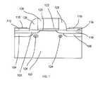
- FIG. 1is a diagram of a typical planar MOSFET geometry.
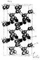
- FIG. 2is a diagram of the 4-to-1 Silicon to Oxygen structure of a preferred embodiment of the invention.
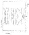
- FIGS. 3 a - care diagrams of the energy bands of the 4-to-1 Silicon to Oxygen structure of a preferred embodiment of the invention.
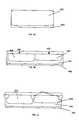
- FIGS. 4 a - hare diagrams showing various stages of fabrication of a semiconductor device.
- the present inventionrelates to controlling the properties of semiconductor materials at the atomic or molecular level to achieve improved performance within semiconductor devices. Further, the invention relates to the identification, creation, and use of improved materials for use in the conduction paths of semiconductor devices.
- Effective massis described with various definitions in the literature.
- the inventors' definition of the inverse conductivity effective massis such that a tensorial component of the conductivity of the material is greater for greater values of the corresponding component of the inverse conductivity mass tensor.
- the inverse of the appropriate tensor elementwe refer to as the conductivity effective mass.
- the inventionIn order to characterize semiconductor material structures, the invention relies on the conductivity effective mass for electrons/holes as described above and calculated in the direction of intended carrier transport as a means to distinguish improved materials.
- the typical planar MOSFET geometryincludes a substrate 102 , source/drain regions 104 and 106 , source/drain extensions 108 and 110 , source/drain silicides 112 and 114 , source/drain contacts 116 and 118 , halo implants 124 and 126 , channel region 120 , gate oxide 122 , gate 126 , and spacers 128 .
- the inventorshave identified improved materials or structures for the channel region 120 .
- the inventorshave identified materials or structures having energy band structures for which the conductivity effective masses for electrons and holes that are substantially less than the corresponding values for silicon.
- the materials or structuresare controlled at the atomic or molecular level and may be formed using known techniques of atomic layer deposition.
- the structurescomprise a repeating structure of a plurality of atomic layers of a semiconductor material and a single atomic layer of a material ((non-semiconductor) element or compound) other than the semiconductor material such as oxygen, nitrogen, fluorine, CO or other inorganic or organic elements or compounds which are compatible with the given semiconductor fabrication process.
- This structuremay be repeated two times or many times or combinations formed with different interleaved layers/different materials to form a low conductivity effective mass (high mobility) semiconductor region.
- FIG. 2An example of one such structure is shown in FIG. 2.
- This example structurehas a repeating structure of four atomic layers of silicon and a single atomic later of oxygen.
- This structurecan be formed using known techniques of atomic layer deposition by, for example, forming a first atomic layer of silicon on a substrate, forming a second atomic layer of silicon on the first atomic layer, forming a third atomic layer of silicon on the second layer, forming a fourth atomic layer of silicon on the third layer, forming a fifth atomic layer of oxygen on the fourth layer, and then starting over by forming a sixth layer of silicon on the fifth layer of oxygen.
- This example structureresults in the energy band structure shown in FIGS. 3 a - c .
- This energy band structure of the present inventionhas conductivity effective masses for electrons and holes that are substantially less (less than half) than the corresponding values for silicon.
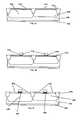
- FIGS. 4 a - hshow how the formation of a channel region of the above structure would fit into a simplified CMOS fabrication process for manufacturing PMOS and NMOS transistors.
- the example process of FIGS. 4 a - hbegins with an eight inch wafer of lightly doped P-type or N-type single crystal silicon with ⁇ 100> orientation 402 .
- the formation of two transistors, one NMOS and one PMOSwill be shown.
- a deep N-well 404is implanted in the substrate 402 for isolation.
- N-well and P-well regions 406 and 408are formed using an SiO 2 /Si 3 N 4 mask prepared using known techniques. This could entail, for example, steps of n-well and p-well implantation, strip, drive-in, clean, and re-growth.
- the strip steprefers to removing the mask (in this case, photoresist and silicon nitride).
- the drive-in stepis used to locate the dopants at the appropriate depth, assuming the implantation is lower energy (i.e. 80 keV) rather than higher energy (200-300 keV). A typical drive-in condition would be approximately 9-10 hrs. @ 1100-1150 C.
- the drive-in stepalso anneals out implantation damage.
- an anneal stepfollows, which is lower temperature and shorter. A clean step comes before any oxidation step so as to avoid contaminating the furnaces with organics, metals, etc. Other known ways or processes for reaching this point may be used as well.
- FIGS. 4 c - hand NMOS device will be shown in one side 200 of the Figures and a PMOS device will be shown in the other side 400 of the Figures.
- FIG. 4 cdepicts shallow trench isolation in which the wafer is patterned, the trenches 410 are etched (0.3-0.8 um), a thin oxide is grown, the trenches are filled with SiO 2 , and then the surface is planarized.
- FIG. 4 ddepicts the definition and deposition of the semiconductor structures of the present invention as the channel regions 412 , 414 .
- FIG. 4 edepicts the devices after the gate oxide layers and the gates are formed.
- a thin gate oxideis deposited, and steps of poly deposition, patterning, and etching are performed.
- Poly depositionrefers to low pressure chemical vapor deposition (LPCVD) of silicon onto an oxide (hence it forms a polycrystalline material).
- LPCVDlow pressure chemical vapor deposition
- the stepincludes doping with P + or As + to make it conducting and the layer is around 250 nm thick. This step depends on the exact process, so the 250 nm thickness is only an example.
- the pattern stepis made up of spinning photoresist, baking it, exposing it to light (photolithography step), and developing the resist. Usually, the patter is then transferred into another layer (oxide or nitride) which acts as an etch mask during the etch step.
- the etch steptypically is a plasma etch (anisotropic, dry etch) that is material selective (e.g. etches silicon 10 times faster than oxide) and transfers the lithography pattern into the material of interest.
- lowly doped source and drain regions 420 and 422are formed. These regions are formed using n-type and p-type LDD implantation, annealing, and cleaning. “LDD” refers to n-type lowly doped drain, or on the source side, p-type lowly doped source. This is a low energy/low dose implant that is the same ion type as the source/drain. An anneal step may be used after the LDD implantation, but depending on the specific process, it may be omitted. The clean step is a chemical etch to remove metals and organics prior to depositing an oxide layer.
- FIG. 4 gshows the spacer formation and the source and drain implants.
- An SiO 2 maskis deposited and etched back.
- N-type and p-type ion implantationis used to form the source and drain regions 430 , 432 , 434 , and 436 .
- the structureis annealed and cleaned.
- FIG. 4 hdepicts the self-aligned silicides formation, also known as salicidation.
- the salicidation processincludes metal deposition (e.g. Ti), nitrogen annealing, metal etching, and a second annealing.
Landscapes
- Insulated Gate Type Field-Effect Transistor (AREA)
- Recrystallisation Techniques (AREA)
Abstract
Description
- None.[0001]
- Not applicable.[0002]
- 1. Field of the Invention[0003]
- The present invention relates broadly to semiconductor structures and devices in which one or more atomic layers of an element or compound other than a semiconductor are interposed between layers of a semiconductor in order to reduce the conductivity effective mass of electrons and/or holes, with a view to improving the carrier mobility of semiconductor structure.[0004]
- 2. Description of the Related Art[0005]
- It is well known in the semiconductor art that for parabolic bands the second derivative, or curvature, of a valence band maximum and conduction band minimum, d[0006]2E/dk2, is inversely proportional to the effective mass. Thus, higher curvature gives a lower effective mass. It is also well known that the carrier transport properties of semiconductors are very sensitive to the effective mass and that, in general, small effective mass is related to high carrier mobility. In practice, the precise relationship between effective mass and carrier mobility is dependent on various scattering mechanisms, doping, electric field, etc., but it is generally understood that the premium on low effective mass in semiconductor materials is high, even under the extreme transport conditions that exist in modern high field (deep) sub-micron MOSFETs.
- Many methods and structures have been used or proposed for improving the operational performance of semiconductor devices. One such method has been to create strain in layers of Si, Ge, or SiGe to alter the carrier mobility in those layers.[0007]
- One such technique is disclosed in published U.S. Patent Application No. 20030057416. The published application discloses a technique which, in a simplified form, provides a silicon substrate, deposits a relaxed graded SiGe buffer layer to a final Ge composition on the silicon substrate, deposits a relaxed SiGe cap layer having a uniform composition on the graded SiGe buffer layer, planarizes the SiGe cap layer, deposits a relaxed SiGe regrowth layer having a uniform composition, and deposits a strained silicon layer on the SiGe regrowth layer. The lattice constant of SiGe is larger than that of Si and is a direct function of the amount of Ge in the SiGe alloy. The graded SiGe buffer layer, which is epitaxially deposited, initially is strained to match the in-plane lattice constant of the underlying silicon substrate. The deposition of the relaxed graded SiGe buffer layer enables engineering of the lattice constant of the SiGe cap layer and, therefore, the amount of strain in the strained silicon layer.[0008]
- The present invention provides semiconductor structures and devices having more desirable effective mass, and hence carrier mobility through the formation of atomic layers of a semiconductor such as silicon and materials other than the semiconductor to create a structure in which atomic layers of materials other than the semiconductor are interposed between atomic layers of the semiconductor. One such material other than a semiconductor is oxygen. Semiconductor materials other than silicon, such as Ge, SiGe, GaAs, SiC, InP, InAs, GaP or related ternary or quaternary alloys and other semiconductor materials may be used. Likewise, materials other than oxygen, such as nitrogen, fluorine, CO or other inorganic or organic elements or compounds which are compatible with a given semiconductor fabrication process may be used.[0009]
- The anisotropic nature of semiconductor materials means that quantities such as effective mass are tensorial in nature rather than scalar quantities. Thus, the direction of fields and carrier transport are an integral feature of the observed carrier transport properties.[0010]
- In order to discriminate between potential structures the inventors use the measure “inverse conductivity effective mass tensor”, which is defined below. The inverse of a component of this tensor corresponding to a preferred direction of transport is referred to as the “conductivity effective mass”.[0011]
- The semiconductor structures of the present invention have conductivity effective masses for electrons and holes that are substantially different than the corresponding values for the base semiconductor.[0012]
- The invention features a semiconductor structure having a first semiconductor layer having a plurality of atomic layers of a semiconductor; a first atomic layer of an (non-semiconductor) element or compound other than the semiconductor on the first semiconductor layer; a second semiconductor layer having a plurality of atomic layers of the semiconductor on the first atomic layer of an (non-semiconductor) element or compound other than the semiconductor; and a second atomic layer of the (non-semiconductor) element or compound other than the semiconductor on the second layer of the semiconductor.[0013]
- In one embodiment, the invention provides a method of forming a semiconductor device having the steps of forming what one may refer to as a super silicon layer by forming a first plurality of atomic layers of silicon on a substrate, forming a first atomic layer of oxygen on the first plurality of atomic layers of silicon, and forming a second plurality of atomic layers of silicon on the atomic layer of oxygen, forming a second atomic layer of oxygen on the second plurality of atomic layers of silicon; forming at least one p-type region in or adjacent to the super silicon layer; forming at least one n-type region in or adjacent to the super silicon layer; and forming a plurality of electrodes.[0014]
- The invention further provides a semiconductor structure having a first atomic layer of silicon; an atomic layer of oxygen on the first atomic layer of silicon; and a second atomic layer of silicon on the atomic layer of oxygen; wherein the semiconductor structure has conductivity effective masses for electrons and holes that are substantially less than the corresponding values for silicon.[0015]
- Still other aspects, features, and advantages of the present invention are readily apparent from the following detailed description, simply by illustrating preferable embodiments and implementations. The present invention is also capable of other and different embodiments, and its several details can be modified in various respects, all without departing from the spirit and scope of the present invention. Accordingly, the drawings and descriptions are to be regarded as illustrative in nature, and not as restrictive.[0016]
- The accompanying drawings, which are incorporated in and constitute a part of this specification illustrate some embodiments of the invention and, together with the description, serve to explain the objects, advantages, and principles of the invention. In the drawings,[0017]
- FIG. 1 is a diagram of a typical planar MOSFET geometry.[0018]
- FIG. 2 is a diagram of the 4-to-1 Silicon to Oxygen structure of a preferred embodiment of the invention.[0019]
- FIGS. 3[0020]a-care diagrams of the energy bands of the 4-to-1 Silicon to Oxygen structure of a preferred embodiment of the invention.
- FIGS. 4[0021]a-hare diagrams showing various stages of fabrication of a semiconductor device.
- The present invention relates to controlling the properties of semiconductor materials at the atomic or molecular level to achieve improved performance within semiconductor devices. Further, the invention relates to the identification, creation, and use of improved materials for use in the conduction paths of semiconductor devices.[0022]
- for holes.[0025]
- The inventors' definition of the inverse conductivity effective mass is such that a tensorial component of the conductivity of the material is greater for greater values of the corresponding component of the inverse conductivity mass tensor. In this patent application we will concentrate on setting the values of the inverse conductivity mass tensor so as to enhance the conductive properties of the material, typically for a preferred direction of carrier transport. The inverse of the appropriate tensor element we refer to as the conductivity effective mass.[0026]
- In order to characterize semiconductor material structures, the invention relies on the conductivity effective mass for electrons/holes as described above and calculated in the direction of intended carrier transport as a means to distinguish improved materials.[0027]
- Using the above-described measures, one can select materials having improved band structures for specific purposes. One such example would be a material for a channel region in a CMOS device. For purposes of explanation, a typical planar MOSFET geometry is shown in FIG. 1. One skilled in the art, however, would know that the materials identified and discovered using the above methods could be used in many different types of integrated circuit devices.[0028]
- As shown in FIG. 1, the typical planar MOSFET geometry includes a[0029]
substrate 102, source/drain regions drain extensions drain silicides drain contacts halo implants channel region 120,gate oxide 122,gate 126, andspacers 128. Using the above-described measures, the inventors have identified improved materials or structures for thechannel region 120. - More specifically, the inventors have identified materials or structures having energy band structures for which the conductivity effective masses for electrons and holes that are substantially less than the corresponding values for silicon.[0030]
- The materials or structures are controlled at the atomic or molecular level and may be formed using known techniques of atomic layer deposition. The structures comprise a repeating structure of a plurality of atomic layers of a semiconductor material and a single atomic layer of a material ((non-semiconductor) element or compound) other than the semiconductor material such as oxygen, nitrogen, fluorine, CO or other inorganic or organic elements or compounds which are compatible with the given semiconductor fabrication process. This structure may be repeated two times or many times or combinations formed with different interleaved layers/different materials to form a low conductivity effective mass (high mobility) semiconductor region.[0031]
- An example of one such structure is shown in FIG. 2. This example structure has a repeating structure of four atomic layers of silicon and a single atomic later of oxygen. This structure can be formed using known techniques of atomic layer deposition by, for example, forming a first atomic layer of silicon on a substrate, forming a second atomic layer of silicon on the first atomic layer, forming a third atomic layer of silicon on the second layer, forming a fourth atomic layer of silicon on the third layer, forming a fifth atomic layer of oxygen on the fourth layer, and then starting over by forming a sixth layer of silicon on the fifth layer of oxygen. This example structure results in the energy band structure shown in FIGS. 3[0032]a-c. This energy band structure of the present invention has conductivity effective masses for electrons and holes that are substantially less (less than half) than the corresponding values for silicon.
- The above, of course, is only one example structure of the invention. Other structures can be formed using different non-semiconductor materials, such as nitrogen instead of oxygen, or a material from the list of nitrogen, fluorine, CO or other inorganic or organic elements or compounds which are compatible with the given semiconductor fabrication process, or using semiconductor material selected from a list of Group IV semiconductor (or IV-IV) such as Si, Ge or SiGe, SiC; Group III-V semiconductor such as GaAs, InP, In As, GaP and related ternary and quaternary alloys, GaN, GaSb and Group II-VI semiconductors such as CdS, CdSe etc. Also, different numbers of atomic layers of silicon or other material may be used, although it is preferable to use fewer than eight atomic layers of silicon.[0033]
- The invention would be one structure within a larger device. As an example, FIGS. 4[0034]a-hshow how the formation of a channel region of the above structure would fit into a simplified CMOS fabrication process for manufacturing PMOS and NMOS transistors. The example process of FIGS. 4a-hbegins with an eight inch wafer of lightly doped P-type or N-type single crystal silicon with <100>
orientation 402. In the example, the formation of two transistors, one NMOS and one PMOS will be shown. In FIG. 4a, a deep N-well404 is implanted in thesubstrate 402 for isolation. In FIG. 4b, N-well and P-well regions - In FIGS. 4[0035]c-h, and NMOS device will be shown in one
side 200 of the Figures and a PMOS device will be shown in theother side 400 of the Figures. FIG. 4cdepicts shallow trench isolation in which the wafer is patterned, thetrenches 410 are etched (0.3-0.8 um), a thin oxide is grown, the trenches are filled with SiO2, and then the surface is planarized. FIG. 4ddepicts the definition and deposition of the semiconductor structures of the present invention as thechannel regions silicon 10 times faster than oxide) and transfers the lithography pattern into the material of interest. - In FIG. 4[0036]f, lowly doped source and drain
regions 420 and422 are formed. These regions are formed using n-type and p-type LDD implantation, annealing, and cleaning. “LDD” refers to n-type lowly doped drain, or on the source side, p-type lowly doped source. This is a low energy/low dose implant that is the same ion type as the source/drain. An anneal step may be used after the LDD implantation, but depending on the specific process, it may be omitted. The clean step is a chemical etch to remove metals and organics prior to depositing an oxide layer. - FIG. 4[0037]gshows the spacer formation and the source and drain implants. An SiO2mask is deposited and etched back. N-type and p-type ion implantation is used to form the source and drain
regions - This, of course, is just one example of a process and device in which the present invention may be used, and those of skill in the art will understand its application and use in many other processes and devices. The invention is by no means limited to the process or structures of FIGS. 1 and 4[0038]a-l. In other processes and devices the structures of the present invention may be formed on a portion of a wafer or across substantially all of a wafer.
- The foregoing description of the preferred embodiment of the invention has been presented for purposes of illustration and description. It is not intended to be exhaustive or to limit the invention to the precise form disclosed, and modifications and variations are possible in light of the above teachings or may be acquired from practice of the invention. The embodiment was chosen and described in order to explain the principles of the invention and its practical application to enable one skilled in the art to utilize the invention in various embodiments as are suited to the particular use contemplated. It is intended that the scope of the invention be defined by the claims appended hereto, and their equivalents. The entirety of each of the aforementioned documents is incorporated by reference herein.[0039]


Claims (11)
1. A method of producing a semiconductor device comprising the steps of:
forming a semiconductor layer by
forming a first plurality of atomic layers of a semiconductor on a substrate;
forming a first atomic layer of a non-semiconductor on said plurality of atomic layers of a semiconductor;
forming a second plurality of atomic layers of a semiconductor on said atomic layer of said non-semiconductor; and
forming a second atomic layer of a non-semiconductor on said second plurality of atomic layers of a semiconductor;
forming at least one p-type region in or directly adjacent to said semiconductor layer;
forming at least one n-type region in or directly adjacent to said semiconductor layer; and
forming a plurality of electrodes.
2. A method according toclaim 1 wherein said step of forming a first plurality of atomic layers of a semiconductor on a substrate comprises the step of forming a plurality of atomic layers of a silicon on a substrate.
3. A method according toclaim 1 wherein said step of forming a first plurality of atomic layers of a semiconductor on a substrate comprises the step of forming fewer than eight atomic layers of said semiconductor on a substrate.
4. A method according toclaim 1 wherein said step of forming a first plurality of atomic layers of a semiconductor on a substrate comprises the step of forming on a substrate a plurality of atomic layers of a semiconductor selected from the group of: Group IV semiconductors, Group VI semiconductors, Group II-V semiconductors, and Group II-VI semiconductors.
5. A method according toclaim 1 wherein said step of forming a first plurality of atomic layers of a semiconductor on a substrate comprises the step of forming on a substrate a plurality of atomic layers of a semiconductor selected from the group of Si, Ge, SiGe, GaAs, InP, InAs, GaP, GaN, GaSb, CdS, and CdSe.
6. A method according toclaim 1 wherein said step of forming a first atomic layer of a non-semiconductor on said plurality of atomic layers of a semiconductor comprises the step of forming a first atomic layer of oxygen on said plurality of atomic layers of a semiconductor.
7. A method according toclaim 1 wherein said step of forming a first atomic layer of a non-semiconductor on said plurality of atomic layers of a semiconductor comprises the step of forming on said plurality of layers of a semiconductor a first atomic layer of one or more selected from the group of: oxygen, nitrogen, fluorine, and CO.
8. A method of forming a semiconductor structure comprising the steps of:
forming first, second, third and fourth atomic layers of silicon;
forming a fifth atomic layer of oxygen on said fourth atomic layer of silicon on a substrate; and
forming sixth, seventh, eighth, and ninth atomic layers of silicon on said fifth atomic layer of oxygen.
forming a tenth atomic layer of oxygen on said ninth atomic layer of silicon.
9. A method of forming a channel region comprising the steps of:
forming first, second, third and fourth atomic layers of silicon;
forming a fifth atomic layer of oxygen on said fourth atomic layer of silicon; and
forming sixth, seventh, eighth, and ninth atomic layers of silicon on said fifth atomic layer of oxygen.
10. A method of forming a high-conductivity region comprising the steps of:
forming a first plurality of atomic layers of a semiconductor on a substrate;
forming a first atomic layer of a non-semiconductor on said plurality of atomic layers of a semiconductor;
forming a second plurality of atomic layers of a semiconductor on said atomic layer of said non-semiconductor; and
forming a second atomic layer of a non-semiconductor on said second plurality of atomic layers of a semiconductor.
11. A method according toclaim 9 , wherein said high-conductivity region is a channel region.
Priority Applications (92)
| Application Number | Priority Date | Filing Date | Title |
|---|---|---|---|
| US10/603,621US20040266116A1 (en) | 2003-06-26 | 2003-06-26 | Methods of fabricating semiconductor structures having improved conductivity effective mass |
| US10/647,060US6958486B2 (en) | 2003-06-26 | 2003-08-22 | Semiconductor device including band-engineered superlattice |
| US10/647,069US6897472B2 (en) | 2003-06-26 | 2003-08-22 | Semiconductor device including MOSFET having band-engineered superlattice |
| US10/647,061US6830964B1 (en) | 2003-06-26 | 2003-08-22 | Method for making semiconductor device including band-engineered superlattice |
| US10/716,994US6952018B2 (en) | 2003-06-26 | 2003-11-19 | Semiconductor device including band-engineered superlattice |
| US10/716,991US6878576B1 (en) | 2003-06-26 | 2003-11-19 | Method for making semiconductor device including band-engineered superlattice |
| US10/717,370US7033437B2 (en) | 2003-06-26 | 2003-11-19 | Method for making semiconductor device including band-engineered superlattice |
| US10/717,375US6927413B2 (en) | 2003-06-26 | 2003-11-19 | Semiconductor device including band-engineered superlattice |
| US10/717,374US6891188B2 (en) | 2003-06-26 | 2003-11-19 | Semiconductor device including band-engineered superlattice |
| US10/716,783US6833294B1 (en) | 2003-06-26 | 2003-11-19 | Method for making semiconductor device including band-engineered superlattice |
| EP04809463AEP1644984B1 (en) | 2003-06-26 | 2004-06-28 | Semiconductor device including superlattice |
| PCT/US2004/020634WO2005018004A1 (en) | 2003-06-26 | 2004-06-28 | Method for making semiconductor device including band-engineered superlattice |
| AU2004301905AAU2004301905B2 (en) | 2003-06-26 | 2004-06-28 | Semiconductor device including band-engineered superlattice |
| DE602004017472TDE602004017472D1 (en) | 2003-06-26 | 2004-06-28 | SEMICONDUCTOR COMPONENT WITH A MOSFET WITH BANDBAG ADJUSTED OVERGATE |
| CN200480018053.0ACN1813354B (en) | 2003-06-26 | 2004-06-28 | Method for making semiconductor device including band-engineered superlattice |
| DE602004025349TDE602004025349D1 (en) | 2003-06-26 | 2004-06-28 | SEMICONDUCTOR COMPONENT WITH BANDBAG ADAPTED OVER |
| DE602004016855TDE602004016855D1 (en) | 2003-06-26 | 2004-06-28 | METHOD FOR PRODUCING A SEMICONDUCTOR COMPONENT WITH RIBBON DESIGNED SUPER GRILLE |
| CA2530065ACA2530065C (en) | 2003-06-26 | 2004-06-28 | Semiconductor device including mosfet having band-engineered superlattice |
| CA002530061ACA2530061A1 (en) | 2003-06-26 | 2004-06-28 | Method for making semiconductor device including band-engineered superlattice |
| JP2006515379AJP4918355B2 (en) | 2003-06-26 | 2004-06-28 | Semiconductor device having a band design superlattice |
| AU2004300982AAU2004300982B2 (en) | 2003-06-26 | 2004-06-28 | Semiconductor device including MOSFET having band-engineered superlattice |
| CA2530067ACA2530067C (en) | 2003-06-26 | 2004-06-28 | Semiconductor device including band-engineered superlattice |
| PCT/US2004/020631WO2005013371A2 (en) | 2003-06-26 | 2004-06-28 | Semiconductor device including band-engineered superlattice |
| CN2004800180155ACN1813353B (en) | 2003-06-26 | 2004-06-28 | Method for making semiconductor device including band-engineered superlattice |
| JP2006515376AJP4742035B2 (en) | 2003-06-26 | 2004-06-28 | Semiconductor device having a band design superlattice |
| CN2004800180935ACN1813355B (en) | 2003-06-26 | 2004-06-28 | Semiconductor device including MOSFET with band engineered superlattice |
| AU2004306355AAU2004306355B2 (en) | 2003-06-26 | 2004-06-28 | Semiconductor device including band-engineered superlattice |
| PCT/US2004/020641WO2005018005A1 (en) | 2003-06-26 | 2004-06-28 | Semiconductor device including mosfet having band-engineered superlattice |
| DE602004023200TDE602004023200D1 (en) | 2003-06-26 | 2004-06-28 | SEMICONDUCTOR COMPONENT WITH SUPER GRILLE |
| EP04785967AEP1644982B1 (en) | 2003-06-26 | 2004-06-28 | Method for making semiconductor device including band-engineered superlattice |
| JP2006515377AJP4918354B2 (en) | 2003-06-26 | 2004-06-28 | Method for fabricating a semiconductor device having a band design superlattice |
| EP04785968AEP1644983B1 (en) | 2003-06-26 | 2004-06-28 | Semiconductor device including mosfet having bandgap-engineered superlattice |
| PCT/US2004/020652WO2005034245A1 (en) | 2003-06-26 | 2004-06-28 | Semiconductor device including band-engineered superlattice |
| AU2004300981AAU2004300981B2 (en) | 2003-06-26 | 2004-06-28 | Method for making semiconductor device including band-engineered superlattice |
| EP04785966AEP1644981B1 (en) | 2003-06-26 | 2004-06-28 | Semiconductor device including band-engineered superlattice and method of manufacturing the same |
| CN2004800179321ACN1813352B (en) | 2003-06-26 | 2004-06-28 | Semiconductor devices including band-engineered superlattices |
| JP2006515378AJP2007521648A (en) | 2003-06-26 | 2004-06-28 | Semiconductor device having MOSFET with band design superlattice |
| CA002530050ACA2530050A1 (en) | 2003-06-26 | 2004-06-28 | Semiconductor device including band-engineered superlattice |
| US10/936,920US7109052B2 (en) | 2003-06-26 | 2004-09-09 | Method for making an integrated circuit comprising a waveguide having an energy band engineered superlattice |
| US10/936,913US7446334B2 (en) | 2003-06-26 | 2004-09-09 | Electronic device comprising active optical devices with an energy band engineered superlattice |
| US10/937,071US7279699B2 (en) | 2003-06-26 | 2004-09-09 | Integrated circuit comprising a waveguide having an energy band engineered superlattice |
| US10/937,072US20050029510A1 (en) | 2003-06-26 | 2004-09-09 | Method for making electronic device comprising active optical devices with an energy band engineered superlattice |
| US10/936,933US20050032247A1 (en) | 2003-06-26 | 2004-09-09 | Method for making an integrated circuit comprising an active optical device having an energy band engineered superlattice |
| US10/936,903US7432524B2 (en) | 2003-06-26 | 2004-09-09 | Integrated circuit comprising an active optical device having an energy band engineered superlattice |
| US10/941,062US7279701B2 (en) | 2003-06-26 | 2004-09-14 | Semiconductor device comprising a superlattice with upper portions extending above adjacent upper portions of source and drain regions |
| US10/940,418US7018900B2 (en) | 2003-06-26 | 2004-09-14 | Method for making a semiconductor device comprising a superlattice channel vertically stepped above source and drain regions |
| US10/940,426US7436026B2 (en) | 2003-06-26 | 2004-09-14 | Semiconductor device comprising a superlattice channel vertically stepped above source and drain regions |
| US10/940,594US7288457B2 (en) | 2003-06-26 | 2004-09-14 | Method for making semiconductor device comprising a superlattice with upper portions extending above adjacent upper portions of source and drain regions |
| US10/992,422US7071119B2 (en) | 2003-06-26 | 2004-11-18 | Method for making a semiconductor device including band-engineered superlattice having 3/1-5/1 germanium layer structure |
| US10/992,186US7034329B2 (en) | 2003-06-26 | 2004-11-18 | Semiconductor device including band-engineered superlattice having 3/1-5/1 germanium layer structure |
| US11/042,270US7435988B2 (en) | 2003-06-26 | 2005-01-25 | Semiconductor device including a MOSFET having a band-engineered superlattice with a semiconductor cap layer providing a channel |
| US11/042,272US7265002B2 (en) | 2003-06-26 | 2005-01-25 | Method for making a semiconductor device including a MOSFET having a band-engineered superlattice with a semiconductor cap layer providing a channel |
| US11/089,950US7303948B2 (en) | 2003-06-26 | 2005-03-25 | Semiconductor device including MOSFET having band-engineered superlattice |
| US11/096,828US7045377B2 (en) | 2003-06-26 | 2005-04-01 | Method for making a semiconductor device including a superlattice and adjacent semiconductor layer with doped regions defining a semiconductor junction |
| US11/097,433US7045813B2 (en) | 2003-06-26 | 2005-04-01 | Semiconductor device including a superlattice with regions defining a semiconductor junction |
| US11/097,612US7229902B2 (en) | 2003-06-26 | 2005-04-01 | Method for making a semiconductor device including a superlattice with regions defining a semiconductor junction |
| US11/097,588US7227174B2 (en) | 2003-06-26 | 2005-04-01 | Semiconductor device including a superlattice and adjacent semiconductor layer with doped regions defining a semiconductor junction |
| US11/136,747US7446002B2 (en) | 2003-06-26 | 2005-05-25 | Method for making a semiconductor device comprising a superlattice dielectric interface layer |
| US11/136,757US20050279991A1 (en) | 2003-06-26 | 2005-05-25 | Semiconductor device including a superlattice having at least one group of substantially undoped layers |
| US11/136,748US20050282330A1 (en) | 2003-06-26 | 2005-05-25 | Method for making a semiconductor device including a superlattice having at least one group of substantially undoped layers |
| US11/136,881US20060011905A1 (en) | 2003-06-26 | 2005-05-25 | Semiconductor device comprising a superlattice dielectric interface layer |
| US11/136,834US7153763B2 (en) | 2003-06-26 | 2005-05-25 | Method for making a semiconductor device including band-engineered superlattice using intermediate annealing |
| US11/380,992US20060273299A1 (en) | 2003-06-26 | 2006-05-01 | Method for making a semiconductor device including a dopant blocking superlattice |
| US11/380,987US20060220118A1 (en) | 2003-06-26 | 2006-05-01 | Semiconductor device including a dopant blocking superlattice |
| US11/381,835US7586116B2 (en) | 2003-06-26 | 2006-05-05 | Semiconductor device having a semiconductor-on-insulator configuration and a superlattice |
| US11/381,850US20060243964A1 (en) | 2003-06-26 | 2006-05-05 | Method for making a semiconductor device having a semiconductor-on-insulator configuration and a superlattice |
| US11/381,794US20060263980A1 (en) | 2003-06-26 | 2006-05-05 | Method for making a semiconductor device including a floating gate memory cell with a superlattice channel |
| US11/381,787US7659539B2 (en) | 2003-06-26 | 2006-05-05 | Semiconductor device including a floating gate memory cell with a superlattice channel |
| US11/420,891US20060231857A1 (en) | 2003-06-26 | 2006-05-30 | Method for making a semiconductor device including a memory cell with a negative differential resistance (ndr) device |
| US11/420,876US7531850B2 (en) | 2003-06-26 | 2006-05-30 | Semiconductor device including a memory cell with a negative differential resistance (NDR) device |
| US11/421,234US7586165B2 (en) | 2003-06-26 | 2006-05-31 | Microelectromechanical systems (MEMS) device including a superlattice |
| US11/421,263US20060223215A1 (en) | 2003-06-26 | 2006-05-31 | Method for Making a Microelectromechanical Systems (MEMS) Device Including a Superlattice |
| US11/425,209US7514328B2 (en) | 2003-06-26 | 2006-06-20 | Method for making a semiconductor device including shallow trench isolation (STI) regions with a superlattice therebetween |
| US11/425,201US20060267130A1 (en) | 2003-06-26 | 2006-06-20 | Semiconductor Device Including Shallow Trench Isolation (STI) Regions with a Superlattice Therebetween |
| US11/426,969US7202494B2 (en) | 2003-06-26 | 2006-06-28 | FINFET including a superlattice |
| US11/426,976US20060292765A1 (en) | 2003-06-26 | 2006-06-28 | Method for Making a FINFET Including a Superlattice |
| US11/428,003US7491587B2 (en) | 2003-06-26 | 2006-06-30 | Method for making a semiconductor device having a semiconductor-on-insulator (SOI) configuration and including a superlattice on a thin semiconductor layer |
| US11/428,015US20060289049A1 (en) | 2003-06-26 | 2006-06-30 | Semiconductor Device Having a Semiconductor-on-Insulator (SOI) Configuration and Including a Superlattice on a Thin Semiconductor Layer |
| US11/457,315US20070020833A1 (en) | 2003-06-26 | 2006-07-13 | Method for Making a Semiconductor Device Including a Channel with a Non-Semiconductor Layer Monolayer |
| US11/457,256US7612366B2 (en) | 2003-06-26 | 2006-07-13 | Semiconductor device including a strained superlattice layer above a stress layer |
| US11/457,293US20070020860A1 (en) | 2003-06-26 | 2006-07-13 | Method for Making Semiconductor Device Including a Strained Superlattice and Overlying Stress Layer and Related Methods |
| US11/457,269US7531828B2 (en) | 2003-06-26 | 2006-07-13 | Semiconductor device including a strained superlattice between at least one pair of spaced apart stress regions |
| US11/457,286US7598515B2 (en) | 2003-06-26 | 2006-07-13 | Semiconductor device including a strained superlattice and overlying stress layer and related methods |
| US11/457,276US20070015344A1 (en) | 2003-06-26 | 2006-07-13 | Method for Making a Semiconductor Device Including a Strained Superlattice Between at Least One Pair of Spaced Apart Stress Regions |
| US11/457,299US20070012910A1 (en) | 2003-06-26 | 2006-07-13 | Semiconductor Device Including a Channel with a Non-Semiconductor Layer Monolayer |
| US11/457,263US20070010040A1 (en) | 2003-06-26 | 2006-07-13 | Method for Making a Semiconductor Device Including a Strained Superlattice Layer Above a Stress Layer |
| US11/534,298US7531829B2 (en) | 2003-06-26 | 2006-09-22 | Semiconductor device including regions of band-engineered semiconductor superlattice to reduce device-on resistance |
| US11/534,343US7535041B2 (en) | 2003-06-26 | 2006-09-22 | Method for making a semiconductor device including regions of band-engineered semiconductor superlattice to reduce device-on resistance |
| US11/534,819US20070063186A1 (en) | 2003-06-26 | 2006-09-25 | Method for making a semiconductor device including a front side strained superlattice layer and a back side stress layer |
| US11/534,796US20070063185A1 (en) | 2003-06-26 | 2006-09-25 | Semiconductor device including a front side strained superlattice layer and a back side stress layer |
| JP2010237839AJP2011044728A (en) | 2003-06-26 | 2010-10-22 | Semiconductor device with band-engineered superlattice |
| JP2010237837AJP2011044727A (en) | 2003-06-26 | 2010-10-22 | Method of making semiconductor device |
Applications Claiming Priority (1)
| Application Number | Priority Date | Filing Date | Title |
|---|---|---|---|
| US10/603,621US20040266116A1 (en) | 2003-06-26 | 2003-06-26 | Methods of fabricating semiconductor structures having improved conductivity effective mass |
Related Parent Applications (3)
| Application Number | Title | Priority Date | Filing Date |
|---|---|---|---|
| US10/603,696ContinuationUS20040262594A1 (en) | 2003-06-26 | 2003-06-26 | Semiconductor structures having improved conductivity effective mass and methods for fabricating same |
| US10/603,696Continuation-In-PartUS20040262594A1 (en) | 2003-06-26 | 2003-06-26 | Semiconductor structures having improved conductivity effective mass and methods for fabricating same |
| US11/457,269ContinuationUS7531828B2 (en) | 2003-06-26 | 2006-07-13 | Semiconductor device including a strained superlattice between at least one pair of spaced apart stress regions |
Related Child Applications (7)
| Application Number | Title | Priority Date | Filing Date |
|---|---|---|---|
| US10/603,696Continuation-In-PartUS20040262594A1 (en) | 2003-06-26 | 2003-06-26 | Semiconductor structures having improved conductivity effective mass and methods for fabricating same |
| US10/603,696ContinuationUS20040262594A1 (en) | 2003-06-26 | 2003-06-26 | Semiconductor structures having improved conductivity effective mass and methods for fabricating same |
| US10/647,061Continuation-In-PartUS6830964B1 (en) | 2003-06-26 | 2003-08-22 | Method for making semiconductor device including band-engineered superlattice |
| US10/647,069Continuation-In-PartUS6897472B2 (en) | 2003-06-26 | 2003-08-22 | Semiconductor device including MOSFET having band-engineered superlattice |
| US10/647,069ContinuationUS6897472B2 (en) | 2003-06-26 | 2003-08-22 | Semiconductor device including MOSFET having band-engineered superlattice |
| US10/647,060Continuation-In-PartUS6958486B2 (en) | 2003-06-26 | 2003-08-22 | Semiconductor device including band-engineered superlattice |
| US11/381,794Continuation-In-PartUS20060263980A1 (en) | 2003-06-26 | 2006-05-05 | Method for making a semiconductor device including a floating gate memory cell with a superlattice channel |
Publications (1)
| Publication Number | Publication Date |
|---|---|
| US20040266116A1true US20040266116A1 (en) | 2004-12-30 |
Family
ID=33539780
Family Applications (1)
| Application Number | Title | Priority Date | Filing Date |
|---|---|---|---|
| US10/603,621AbandonedUS20040266116A1 (en) | 2003-06-26 | 2003-06-26 | Methods of fabricating semiconductor structures having improved conductivity effective mass |
Country Status (2)
| Country | Link |
|---|---|
| US (1) | US20040266116A1 (en) |
| CN (3) | CN1813352B (en) |
Cited By (35)
| Publication number | Priority date | Publication date | Assignee | Title |
|---|---|---|---|---|
| US20050035369A1 (en)* | 2003-08-15 | 2005-02-17 | Chun-Chieh Lin | Structure and method of forming integrated circuits utilizing strained channel transistors |
| US20050035410A1 (en)* | 2003-08-15 | 2005-02-17 | Yee-Chia Yeo | Semiconductor diode with reduced leakage |
| US20050093067A1 (en)* | 2003-04-30 | 2005-05-05 | Yee-Chia Yeo | Semiconductor-on-insulator chip incorporating strained-channel partially-depleted, fully-depleted, and multiple-gate transistors |
| US20050282330A1 (en)* | 2003-06-26 | 2005-12-22 | Rj Mears, Llc | Method for making a semiconductor device including a superlattice having at least one group of substantially undoped layers |
| US20060226487A1 (en)* | 2003-08-18 | 2006-10-12 | Yee-Chia Yeo | Resistor with reduced leakage |
| US20060265803A1 (en)* | 2005-05-25 | 2006-11-30 | Gestion Ultra Internationale Inc. | Hydromassaging bathing tub with adjustable elevated seat |
| US20070063186A1 (en)* | 2003-06-26 | 2007-03-22 | Rj Mears, Llc | Method for making a semiconductor device including a front side strained superlattice layer and a back side stress layer |
| US20070063185A1 (en)* | 2003-06-26 | 2007-03-22 | Rj Mears, Llc | Semiconductor device including a front side strained superlattice layer and a back side stress layer |
| US7354843B2 (en) | 2003-07-25 | 2008-04-08 | Taiwan Semiconductor Manufacturing Company, Ltd. | Method of forming a capacitor that includes forming a bottom electrode in a strained silicon layer |
| US7646068B2 (en) | 2003-08-15 | 2010-01-12 | Taiwan Semiconductor Manufacturing Company, Ltd. | Structure and method of a strained channel transistor and a second semiconductor component in an integrated circuit |
| US7745279B2 (en) | 2003-07-25 | 2010-06-29 | Taiwan Semiconductor Manufacturing Company, Ltd. | Capacitor that includes high permittivity capacitor dielectric |
| US7808051B2 (en) | 2008-09-29 | 2010-10-05 | Taiwan Semiconductor Manufacturing Company, Ltd. | Standard cell without OD space effect in Y-direction |
| US7867860B2 (en) | 2003-07-25 | 2011-01-11 | Taiwan Semiconductor Manufacturing Company, Ltd. | Strained channel transistor formation |
| US7888201B2 (en) | 2003-11-04 | 2011-02-15 | Taiwan Semiconductor Manufacturing Company, Ltd. | Semiconductor-on-insulator SRAM configured using partially-depleted and fully-depleted transistors |
| US7943961B2 (en) | 2008-03-13 | 2011-05-17 | Taiwan Semiconductor Manufacturing Company, Ltd. | Strain bars in stressed layers of MOS devices |
| US20120244670A1 (en)* | 2011-03-22 | 2012-09-27 | Samsung Electronics Co., Ltd. | Methods of fabricating semiconductor devices |
| US8558278B2 (en) | 2007-01-16 | 2013-10-15 | Taiwan Semiconductor Manufacturing Company, Ltd. | Strained transistor with optimized drive current and method of forming |
| US9275996B2 (en) | 2013-11-22 | 2016-03-01 | Mears Technologies, Inc. | Vertical semiconductor devices including superlattice punch through stop layer and related methods |
| US9406753B2 (en) | 2013-11-22 | 2016-08-02 | Atomera Incorporated | Semiconductor devices including superlattice depletion layer stack and related methods |
| US9558939B1 (en) | 2016-01-15 | 2017-01-31 | Atomera Incorporated | Methods for making a semiconductor device including atomic layer structures using N2O as an oxygen source |
| US9716147B2 (en) | 2014-06-09 | 2017-07-25 | Atomera Incorporated | Semiconductor devices with enhanced deterministic doping and related methods |
| US9722046B2 (en) | 2014-11-25 | 2017-08-01 | Atomera Incorporated | Semiconductor device including a superlattice and replacement metal gate structure and related methods |
| US9721790B2 (en) | 2015-06-02 | 2017-08-01 | Atomera Incorporated | Method for making enhanced semiconductor structures in single wafer processing chamber with desired uniformity control |
| US9899479B2 (en) | 2015-05-15 | 2018-02-20 | Atomera Incorporated | Semiconductor devices with superlattice layers providing halo implant peak confinement and related methods |
| US10916642B2 (en) | 2019-04-18 | 2021-02-09 | Globalfoundries U.S. Inc. | Heterojunction bipolar transistor with emitter base junction oxide interface |
| CN112789730A (en)* | 2018-08-30 | 2021-05-11 | 阿托梅拉公司 | Method and device for manufacturing superlattice structure with reduced defect density |
| US11158722B2 (en) | 2019-12-30 | 2021-10-26 | Globalfoundries U.S. Inc. | Transistors with lattice structure |
| CN113871460A (en)* | 2019-05-06 | 2021-12-31 | 林和 | Superlattice VLSI |
| US11264499B2 (en) | 2019-09-16 | 2022-03-01 | Globalfoundries U.S. Inc. | Transistor devices with source/drain regions comprising an interface layer that comprises a non-semiconductor material |
| US11978771B2 (en) | 2020-07-02 | 2024-05-07 | Atomera Incorporated | Gate-all-around (GAA) device including a superlattice |
| US12142669B2 (en) | 2023-03-24 | 2024-11-12 | Atomera Incorporated | Method for making nanostructure transistors with flush source/drain dopant blocking structures including a superlattice |
| US12267996B2 (en) | 2022-05-04 | 2025-04-01 | Atomera Incorporated | DRAM sense amplifier architecture with reduced power consumption and related methods |
| US12308229B2 (en) | 2023-07-03 | 2025-05-20 | Atomera Incorporated | Method for making memory device including a superlattice gettering layer |
| US12315722B2 (en) | 2023-03-14 | 2025-05-27 | Atomera Incorporated | Method for making a radio frequency silicon-on-insulator (RFSOI) wafer including a superlattice |
| US12382689B2 (en) | 2023-05-08 | 2025-08-05 | Atomera Incorporated | Method for making DMOS devices including a superlattice and field plate for drift region diffusion |
Families Citing this family (2)
| Publication number | Priority date | Publication date | Assignee | Title |
|---|---|---|---|---|
| US7834345B2 (en)* | 2008-09-05 | 2010-11-16 | Taiwan Semiconductor Manufacturing Company, Ltd. | Tunnel field-effect transistors with superlattice channels |
| WO2019118840A1 (en)* | 2017-12-15 | 2019-06-20 | Atomera Incorporated | Cmos image sensor including stacked semiconductor chips and readout circuitry including a superlattice and related methods |
Citations (32)
| Publication number | Priority date | Publication date | Assignee | Title |
|---|---|---|---|---|
| US505887A (en)* | 1893-10-03 | Drawing-rolls | ||
| US4485128A (en)* | 1981-11-20 | 1984-11-27 | Chronar Corporation | Bandgap control in amorphous semiconductors |
| US4594603A (en)* | 1982-04-22 | 1986-06-10 | Board Of Trustees Of The University Of Illinois | Semiconductor device with disordered active region |
| US4882609A (en)* | 1984-11-19 | 1989-11-21 | Max-Planck Gesellschaft Zur Forderung Der Wissenschafter E.V. | Semiconductor devices with at least one monoatomic layer of doping atoms |
| US4908678A (en)* | 1986-10-08 | 1990-03-13 | Semiconductor Energy Laboratory Co., Ltd. | FET with a super lattice channel |
| US4937204A (en)* | 1985-03-15 | 1990-06-26 | Sony Corporation | Method of making a superlattice heterojunction bipolar device |
| US4969031A (en)* | 1982-02-03 | 1990-11-06 | Hitachi, Ltd. | Semiconductor devices and method for making the same |
| US5081513A (en)* | 1991-02-28 | 1992-01-14 | Xerox Corporation | Electronic device with recovery layer proximate to active layer |
| US5216262A (en)* | 1992-03-02 | 1993-06-01 | Raphael Tsu | Quantum well structures useful for semiconductor devices |
| US5357119A (en)* | 1993-02-19 | 1994-10-18 | Board Of Regents Of The University Of California | Field effect devices having short period superlattice structures using Si and Ge |
| US5606177A (en)* | 1993-10-29 | 1997-02-25 | Texas Instruments Incorporated | Silicon oxide resonant tunneling diode structure |
| US5683934A (en)* | 1994-09-26 | 1997-11-04 | Motorola, Inc. | Enhanced mobility MOSFET device and method |
| US5684817A (en)* | 1995-05-12 | 1997-11-04 | Thomson-Csf | Semiconductor laser having a structure of photonic bandgap material |
| US5994164A (en)* | 1997-03-18 | 1999-11-30 | The Penn State Research Foundation | Nanostructure tailoring of material properties using controlled crystallization |
| US6058127A (en)* | 1996-12-13 | 2000-05-02 | Massachusetts Institute Of Technology | Tunable microcavity and method of using nonlinear materials in a photonic crystal |
| US6255150B1 (en)* | 1997-10-23 | 2001-07-03 | Texas Instruments Incorporated | Use of crystalline SiOx barriers for Si-based resonant tunneling diodes |
| US6274007B1 (en)* | 1999-11-25 | 2001-08-14 | Sceptre Electronics Limited | Methods of formation of a silicon nanostructure, a silicon quantum wire array and devices based thereon |
| US6281532B1 (en)* | 1999-06-28 | 2001-08-28 | Intel Corporation | Technique to obtain increased channel mobilities in NMOS transistors by gate electrode engineering |
| US6281518B1 (en)* | 1997-12-04 | 2001-08-28 | Ricoh Company, Ltd. | Layered III-V semiconductor structures and light emitting devices including the structures |
| US6326311B1 (en)* | 1998-03-30 | 2001-12-04 | Sharp Kabushiki Kaisha | Microstructure producing method capable of controlling growth position of minute particle or thin and semiconductor device employing the microstructure |
| US6344271B1 (en)* | 1998-11-06 | 2002-02-05 | Nanoenergy Corporation | Materials and products using nanostructured non-stoichiometric substances |
| US6350993B1 (en)* | 1999-03-12 | 2002-02-26 | International Business Machines Corporation | High speed composite p-channel Si/SiGe heterostructure for field effect devices |
| US6376337B1 (en)* | 1997-11-10 | 2002-04-23 | Nanodynamics, Inc. | Epitaxial SiOx barrier/insulation layer |
| US6436784B1 (en)* | 1995-08-03 | 2002-08-20 | Hitachi Europe Limited | Method of forming semiconductor structure |
| US6472685B2 (en)* | 1997-12-03 | 2002-10-29 | Matsushita Electric Industrial Co., Ltd. | Semiconductor device |
| US6498359B2 (en)* | 2000-05-22 | 2002-12-24 | Max-Planck-Gesellschaft Zur Foerderung Der Wissenschaften E.V. | Field-effect transistor based on embedded cluster structures and process for its production |
| US6501092B1 (en)* | 1999-10-25 | 2002-12-31 | Intel Corporation | Integrated semiconductor superlattice optical modulator |
| US6521549B1 (en)* | 2000-11-28 | 2003-02-18 | Lsi Logic Corporation | Method of reducing silicon oxynitride gate insulator thickness in some transistors of a hybrid integrated circuit to obtain increased differential in gate insulator thickness with other transistors of the hybrid circuit |
| US20030034529A1 (en)* | 2000-12-04 | 2003-02-20 | Amberwave Systems Corporation | CMOS inverter and integrated circuits utilizing strained silicon surface channel MOSFETs |
| US20030057416A1 (en)* | 2001-09-21 | 2003-03-27 | Amberwave Systems Corporation | Semiconductor structures employing strained material layers with defined impurity gradients and methods for fabricating same |
| US20030162335A1 (en)* | 1999-01-14 | 2003-08-28 | Matsushita Electric Industrial Co., Ltd. | Semiconductor device and method for fabricating the same |
| US20030215990A1 (en)* | 2002-03-14 | 2003-11-20 | Eugene Fitzgerald | Methods for fabricating strained layers on semiconductor substrates |
Family Cites Families (1)
| Publication number | Priority date | Publication date | Assignee | Title |
|---|---|---|---|---|
| EP0843361A1 (en)* | 1996-11-15 | 1998-05-20 | Hitachi Europe Limited | Memory device |
- 2003
- 2003-06-26USUS10/603,621patent/US20040266116A1/ennot_activeAbandoned
- 2004
- 2004-06-28CNCN2004800179321Apatent/CN1813352B/ennot_activeExpired - Fee Related
- 2004-06-28CNCN2004800180935Apatent/CN1813355B/ennot_activeExpired - Fee Related
- 2004-06-28CNCN2004800180155Apatent/CN1813353B/ennot_activeExpired - Fee Related
Patent Citations (34)
| Publication number | Priority date | Publication date | Assignee | Title |
|---|---|---|---|---|
| US505887A (en)* | 1893-10-03 | Drawing-rolls | ||
| US4485128A (en)* | 1981-11-20 | 1984-11-27 | Chronar Corporation | Bandgap control in amorphous semiconductors |
| US4969031A (en)* | 1982-02-03 | 1990-11-06 | Hitachi, Ltd. | Semiconductor devices and method for making the same |
| US4594603A (en)* | 1982-04-22 | 1986-06-10 | Board Of Trustees Of The University Of Illinois | Semiconductor device with disordered active region |
| US4882609A (en)* | 1984-11-19 | 1989-11-21 | Max-Planck Gesellschaft Zur Forderung Der Wissenschafter E.V. | Semiconductor devices with at least one monoatomic layer of doping atoms |
| US4937204A (en)* | 1985-03-15 | 1990-06-26 | Sony Corporation | Method of making a superlattice heterojunction bipolar device |
| US4908678A (en)* | 1986-10-08 | 1990-03-13 | Semiconductor Energy Laboratory Co., Ltd. | FET with a super lattice channel |
| US5081513A (en)* | 1991-02-28 | 1992-01-14 | Xerox Corporation | Electronic device with recovery layer proximate to active layer |
| US5216262A (en)* | 1992-03-02 | 1993-06-01 | Raphael Tsu | Quantum well structures useful for semiconductor devices |
| US5357119A (en)* | 1993-02-19 | 1994-10-18 | Board Of Regents Of The University Of California | Field effect devices having short period superlattice structures using Si and Ge |
| US5606177A (en)* | 1993-10-29 | 1997-02-25 | Texas Instruments Incorporated | Silicon oxide resonant tunneling diode structure |
| US5683934A (en)* | 1994-09-26 | 1997-11-04 | Motorola, Inc. | Enhanced mobility MOSFET device and method |
| US5684817A (en)* | 1995-05-12 | 1997-11-04 | Thomson-Csf | Semiconductor laser having a structure of photonic bandgap material |
| US6436784B1 (en)* | 1995-08-03 | 2002-08-20 | Hitachi Europe Limited | Method of forming semiconductor structure |
| US6058127A (en)* | 1996-12-13 | 2000-05-02 | Massachusetts Institute Of Technology | Tunable microcavity and method of using nonlinear materials in a photonic crystal |
| US5994164A (en)* | 1997-03-18 | 1999-11-30 | The Penn State Research Foundation | Nanostructure tailoring of material properties using controlled crystallization |
| US6255150B1 (en)* | 1997-10-23 | 2001-07-03 | Texas Instruments Incorporated | Use of crystalline SiOx barriers for Si-based resonant tunneling diodes |
| US6376337B1 (en)* | 1997-11-10 | 2002-04-23 | Nanodynamics, Inc. | Epitaxial SiOx barrier/insulation layer |
| US6472685B2 (en)* | 1997-12-03 | 2002-10-29 | Matsushita Electric Industrial Co., Ltd. | Semiconductor device |
| US6281518B1 (en)* | 1997-12-04 | 2001-08-28 | Ricoh Company, Ltd. | Layered III-V semiconductor structures and light emitting devices including the structures |
| US6326311B1 (en)* | 1998-03-30 | 2001-12-04 | Sharp Kabushiki Kaisha | Microstructure producing method capable of controlling growth position of minute particle or thin and semiconductor device employing the microstructure |
| US6344271B1 (en)* | 1998-11-06 | 2002-02-05 | Nanoenergy Corporation | Materials and products using nanostructured non-stoichiometric substances |
| US20030162335A1 (en)* | 1999-01-14 | 2003-08-28 | Matsushita Electric Industrial Co., Ltd. | Semiconductor device and method for fabricating the same |
| US6350993B1 (en)* | 1999-03-12 | 2002-02-26 | International Business Machines Corporation | High speed composite p-channel Si/SiGe heterostructure for field effect devices |
| US6281532B1 (en)* | 1999-06-28 | 2001-08-28 | Intel Corporation | Technique to obtain increased channel mobilities in NMOS transistors by gate electrode engineering |
| US6566679B2 (en)* | 1999-10-25 | 2003-05-20 | Intel Corporation | Integrated semiconductor superlattice optical modulator |
| US6501092B1 (en)* | 1999-10-25 | 2002-12-31 | Intel Corporation | Integrated semiconductor superlattice optical modulator |
| US6621097B2 (en)* | 1999-10-25 | 2003-09-16 | Intel Corporation | Integrated semiconductor superlattice optical modulator |
| US6274007B1 (en)* | 1999-11-25 | 2001-08-14 | Sceptre Electronics Limited | Methods of formation of a silicon nanostructure, a silicon quantum wire array and devices based thereon |
| US6498359B2 (en)* | 2000-05-22 | 2002-12-24 | Max-Planck-Gesellschaft Zur Foerderung Der Wissenschaften E.V. | Field-effect transistor based on embedded cluster structures and process for its production |
| US6521549B1 (en)* | 2000-11-28 | 2003-02-18 | Lsi Logic Corporation | Method of reducing silicon oxynitride gate insulator thickness in some transistors of a hybrid integrated circuit to obtain increased differential in gate insulator thickness with other transistors of the hybrid circuit |
| US20030034529A1 (en)* | 2000-12-04 | 2003-02-20 | Amberwave Systems Corporation | CMOS inverter and integrated circuits utilizing strained silicon surface channel MOSFETs |
| US20030057416A1 (en)* | 2001-09-21 | 2003-03-27 | Amberwave Systems Corporation | Semiconductor structures employing strained material layers with defined impurity gradients and methods for fabricating same |
| US20030215990A1 (en)* | 2002-03-14 | 2003-11-20 | Eugene Fitzgerald | Methods for fabricating strained layers on semiconductor substrates |
Cited By (53)
| Publication number | Priority date | Publication date | Assignee | Title |
|---|---|---|---|---|
| US20050093067A1 (en)* | 2003-04-30 | 2005-05-05 | Yee-Chia Yeo | Semiconductor-on-insulator chip incorporating strained-channel partially-depleted, fully-depleted, and multiple-gate transistors |
| US7268024B2 (en) | 2003-04-30 | 2007-09-11 | Taiwan Semiconductor Manufacturing Company, Ltd. | Semiconductor-on-insulator chip incorporating strained-channel partially-depleted, fully-depleted, and multiple-gate transistors |
| US20070063185A1 (en)* | 2003-06-26 | 2007-03-22 | Rj Mears, Llc | Semiconductor device including a front side strained superlattice layer and a back side stress layer |
| US20050282330A1 (en)* | 2003-06-26 | 2005-12-22 | Rj Mears, Llc | Method for making a semiconductor device including a superlattice having at least one group of substantially undoped layers |
| US20070063186A1 (en)* | 2003-06-26 | 2007-03-22 | Rj Mears, Llc | Method for making a semiconductor device including a front side strained superlattice layer and a back side stress layer |
| US7867860B2 (en) | 2003-07-25 | 2011-01-11 | Taiwan Semiconductor Manufacturing Company, Ltd. | Strained channel transistor formation |
| US7745279B2 (en) | 2003-07-25 | 2010-06-29 | Taiwan Semiconductor Manufacturing Company, Ltd. | Capacitor that includes high permittivity capacitor dielectric |
| US7354843B2 (en) | 2003-07-25 | 2008-04-08 | Taiwan Semiconductor Manufacturing Company, Ltd. | Method of forming a capacitor that includes forming a bottom electrode in a strained silicon layer |
| US7646068B2 (en) | 2003-08-15 | 2010-01-12 | Taiwan Semiconductor Manufacturing Company, Ltd. | Structure and method of a strained channel transistor and a second semiconductor component in an integrated circuit |
| US20050035369A1 (en)* | 2003-08-15 | 2005-02-17 | Chun-Chieh Lin | Structure and method of forming integrated circuits utilizing strained channel transistors |
| US20050035410A1 (en)* | 2003-08-15 | 2005-02-17 | Yee-Chia Yeo | Semiconductor diode with reduced leakage |
| US20060226487A1 (en)* | 2003-08-18 | 2006-10-12 | Yee-Chia Yeo | Resistor with reduced leakage |
| US7888201B2 (en) | 2003-11-04 | 2011-02-15 | Taiwan Semiconductor Manufacturing Company, Ltd. | Semiconductor-on-insulator SRAM configured using partially-depleted and fully-depleted transistors |
| WO2006127291A3 (en)* | 2005-05-25 | 2007-02-22 | Rj Mears Llc | Method for making a semiconductor device including a superlattice having at least one group of substantially undoped layers |
| US20060265803A1 (en)* | 2005-05-25 | 2006-11-30 | Gestion Ultra Internationale Inc. | Hydromassaging bathing tub with adjustable elevated seat |
| WO2007038656A1 (en)* | 2005-09-26 | 2007-04-05 | Mears Technologies, Inc. | Semiconductor device including a front side strained superlattice layer and a back side stress layer and associated methods |
| US8558278B2 (en) | 2007-01-16 | 2013-10-15 | Taiwan Semiconductor Manufacturing Company, Ltd. | Strained transistor with optimized drive current and method of forming |
| US8389316B2 (en) | 2008-03-13 | 2013-03-05 | Taiwan Semiconductor Manufacturing Company, Ltd. | Strain bars in stressed layers of MOS devices |
| US7943961B2 (en) | 2008-03-13 | 2011-05-17 | Taiwan Semiconductor Manufacturing Company, Ltd. | Strain bars in stressed layers of MOS devices |
| US7808051B2 (en) | 2008-09-29 | 2010-10-05 | Taiwan Semiconductor Manufacturing Company, Ltd. | Standard cell without OD space effect in Y-direction |
| US20120244670A1 (en)* | 2011-03-22 | 2012-09-27 | Samsung Electronics Co., Ltd. | Methods of fabricating semiconductor devices |
| US8778753B2 (en)* | 2011-03-22 | 2014-07-15 | Samsung Electronics Co., Ltd. | Methods of fabricating semiconductor devices |
| US9142461B2 (en) | 2011-03-22 | 2015-09-22 | Samsung Electronics Co., Ltd. | Methods of fabricating semiconductor devices |
| US9275996B2 (en) | 2013-11-22 | 2016-03-01 | Mears Technologies, Inc. | Vertical semiconductor devices including superlattice punch through stop layer and related methods |
| US9406753B2 (en) | 2013-11-22 | 2016-08-02 | Atomera Incorporated | Semiconductor devices including superlattice depletion layer stack and related methods |
| US9972685B2 (en) | 2013-11-22 | 2018-05-15 | Atomera Incorporated | Vertical semiconductor devices including superlattice punch through stop layer and related methods |
| US10170560B2 (en) | 2014-06-09 | 2019-01-01 | Atomera Incorporated | Semiconductor devices with enhanced deterministic doping and related methods |
| US9716147B2 (en) | 2014-06-09 | 2017-07-25 | Atomera Incorporated | Semiconductor devices with enhanced deterministic doping and related methods |
| US9722046B2 (en) | 2014-11-25 | 2017-08-01 | Atomera Incorporated | Semiconductor device including a superlattice and replacement metal gate structure and related methods |
| US10084045B2 (en) | 2014-11-25 | 2018-09-25 | Atomera Incorporated | Semiconductor device including a superlattice and replacement metal gate structure and related methods |
| US9899479B2 (en) | 2015-05-15 | 2018-02-20 | Atomera Incorporated | Semiconductor devices with superlattice layers providing halo implant peak confinement and related methods |
| US9941359B2 (en) | 2015-05-15 | 2018-04-10 | Atomera Incorporated | Semiconductor devices with superlattice and punch-through stop (PTS) layers at different depths and related methods |
| US9721790B2 (en) | 2015-06-02 | 2017-08-01 | Atomera Incorporated | Method for making enhanced semiconductor structures in single wafer processing chamber with desired uniformity control |
| US9558939B1 (en) | 2016-01-15 | 2017-01-31 | Atomera Incorporated | Methods for making a semiconductor device including atomic layer structures using N2O as an oxygen source |
| CN112789730A (en)* | 2018-08-30 | 2021-05-11 | 阿托梅拉公司 | Method and device for manufacturing superlattice structure with reduced defect density |
| US10916642B2 (en) | 2019-04-18 | 2021-02-09 | Globalfoundries U.S. Inc. | Heterojunction bipolar transistor with emitter base junction oxide interface |
| US11848192B2 (en) | 2019-04-18 | 2023-12-19 | Globalfoundries U.S. Inc. | Heterojunction bipolar transistor with emitter base junction oxide interface |
| CN113871461A (en)* | 2019-05-06 | 2021-12-31 | 林和 | Superlattice very large scale integrated circuit |
| CN113871459A (en)* | 2019-05-06 | 2021-12-31 | 林和 | Superlattice VLSI |
| CN113871457A (en)* | 2019-05-06 | 2021-12-31 | 林和 | Superlattice VLSI |
| CN113871458A (en)* | 2019-05-06 | 2021-12-31 | 林和 | Superlattice very large scale integrated circuit |
| CN113871460A (en)* | 2019-05-06 | 2021-12-31 | 林和 | Superlattice VLSI |
| US11264499B2 (en) | 2019-09-16 | 2022-03-01 | Globalfoundries U.S. Inc. | Transistor devices with source/drain regions comprising an interface layer that comprises a non-semiconductor material |
| US11158722B2 (en) | 2019-12-30 | 2021-10-26 | Globalfoundries U.S. Inc. | Transistors with lattice structure |
| US11978771B2 (en) | 2020-07-02 | 2024-05-07 | Atomera Incorporated | Gate-all-around (GAA) device including a superlattice |
| US12142641B2 (en) | 2020-07-02 | 2024-11-12 | Atomera Incorporated | Method for making gate-all-around (GAA) device including a superlattice |
| US12267996B2 (en) | 2022-05-04 | 2025-04-01 | Atomera Incorporated | DRAM sense amplifier architecture with reduced power consumption and related methods |
| US12315722B2 (en) | 2023-03-14 | 2025-05-27 | Atomera Incorporated | Method for making a radio frequency silicon-on-insulator (RFSOI) wafer including a superlattice |
| US12142669B2 (en) | 2023-03-24 | 2024-11-12 | Atomera Incorporated | Method for making nanostructure transistors with flush source/drain dopant blocking structures including a superlattice |
| US12142662B2 (en) | 2023-03-24 | 2024-11-12 | Atomera Incorporated | Method for making nanostructure transistors with offset source/drain dopant blocking structures including a superlattice |
| US12230694B2 (en) | 2023-03-24 | 2025-02-18 | Atomera Incorporated | Method for making nanostructure transistors with source/drain trench contact liners |
| US12382689B2 (en) | 2023-05-08 | 2025-08-05 | Atomera Incorporated | Method for making DMOS devices including a superlattice and field plate for drift region diffusion |
| US12308229B2 (en) | 2023-07-03 | 2025-05-20 | Atomera Incorporated | Method for making memory device including a superlattice gettering layer |
Also Published As
| Publication number | Publication date |
|---|---|
| CN1813353B (en) | 2010-07-07 |
| CN1813355A (en) | 2006-08-02 |
| CN1813352B (en) | 2010-05-26 |
| CN1813352A (en) | 2006-08-02 |
| CN1813353A (en) | 2006-08-02 |
| CN1813355B (en) | 2010-05-26 |
Similar Documents
| Publication | Publication Date | Title |
|---|---|---|
| US20040266116A1 (en) | Methods of fabricating semiconductor structures having improved conductivity effective mass | |
| US20040262594A1 (en) | Semiconductor structures having improved conductivity effective mass and methods for fabricating same | |
| US6833294B1 (en) | Method for making semiconductor device including band-engineered superlattice | |
| US7034329B2 (en) | Semiconductor device including band-engineered superlattice having 3/1-5/1 germanium layer structure | |
| JP5450652B2 (en) | Quantum well MOSFET channel with uniaxial strain generated by metal source / drain and conformal regrowth source / drain | |
| US7265002B2 (en) | Method for making a semiconductor device including a MOSFET having a band-engineered superlattice with a semiconductor cap layer providing a channel | |
| US7112495B2 (en) | Structure and method of a strained channel transistor and a second semiconductor component in an integrated circuit | |
| KR101436129B1 (en) | Stress-type field-effect transistor and manufacturing method thereof | |
| JP5300509B2 (en) | Method for fabricating a semiconductor structure using a strained material layer having a defined impurity gradient | |
| US8232172B2 (en) | Stress enhanced transistor devices and methods of making | |
| US8963248B2 (en) | Semiconductor device having SSOI substrate with relaxed tensile stress | |
| US20120080720A1 (en) | Method of forming a semiconductor device and semiconductor device | |
| EP1478029A1 (en) | Mos transistor and method of fabricating the same | |
| US20050282330A1 (en) | Method for making a semiconductor device including a superlattice having at least one group of substantially undoped layers | |
| US20050279991A1 (en) | Semiconductor device including a superlattice having at least one group of substantially undoped layers | |
| TW200910470A (en) | Enhanced hole mobility p-type JFET and fabrication method therefor | |
| CN102468164A (en) | Transistor and method of manufacturing the same |
Legal Events
| Date | Code | Title | Description |
|---|---|---|---|
| AS | Assignment | Owner name:R.J. MEARS LLC, MASSACHUSETTS Free format text:ASSIGNMENT OF ASSIGNORS INTEREST;ASSIGNORS:MEARS, ROBERT J.;YIPTONG, JEAN AUGUSTIN CHAN SOW FOOK;HYTHA, MAREK;REEL/FRAME:014674/0623 Effective date:20031029 | |
| STCB | Information on status: application discontinuation | Free format text:ABANDONED -- FAILURE TO RESPOND TO AN OFFICE ACTION |