US20040262732A1 - Semiconductor device and manufacturing method thereof - Google Patents
Semiconductor device and manufacturing method thereofDownload PDFInfo
- Publication number
- US20040262732A1 US20040262732A1US10/828,556US82855604AUS2004262732A1US 20040262732 A1US20040262732 A1US 20040262732A1US 82855604 AUS82855604 AUS 82855604AUS 2004262732 A1US2004262732 A1US 2004262732A1
- Authority
- US
- United States
- Prior art keywords
- wiring
- semiconductor device
- semiconductor
- semiconductor chip
- manufacturing
- Prior art date
- Legal status (The legal status is an assumption and is not a legal conclusion. Google has not performed a legal analysis and makes no representation as to the accuracy of the status listed.)
- Granted
Links
Images


Classifications
- H—ELECTRICITY
- H01—ELECTRIC ELEMENTS
- H01L—SEMICONDUCTOR DEVICES NOT COVERED BY CLASS H10
- H01L21/00—Processes or apparatus adapted for the manufacture or treatment of semiconductor or solid state devices or of parts thereof
- H01L21/70—Manufacture or treatment of devices consisting of a plurality of solid state components formed in or on a common substrate or of parts thereof; Manufacture of integrated circuit devices or of parts thereof
- H01L21/71—Manufacture of specific parts of devices defined in group H01L21/70
- H01L21/768—Applying interconnections to be used for carrying current between separate components within a device comprising conductors and dielectrics
- H01L21/76898—Applying interconnections to be used for carrying current between separate components within a device comprising conductors and dielectrics formed through a semiconductor substrate
- E—FIXED CONSTRUCTIONS
- E06—DOORS, WINDOWS, SHUTTERS, OR ROLLER BLINDS IN GENERAL; LADDERS
- E06B—FIXED OR MOVABLE CLOSURES FOR OPENINGS IN BUILDINGS, VEHICLES, FENCES OR LIKE ENCLOSURES IN GENERAL, e.g. DOORS, WINDOWS, BLINDS, GATES
- E06B7/00—Special arrangements or measures in connection with doors or windows
- E06B7/16—Sealing arrangements on wings or parts co-operating with the wings
- E06B7/18—Sealing arrangements on wings or parts co-operating with the wings by means of movable edgings, e.g. draught sealings additionally used for bolting, e.g. by spring force or with operating lever
- E06B7/20—Sealing arrangements on wings or parts co-operating with the wings by means of movable edgings, e.g. draught sealings additionally used for bolting, e.g. by spring force or with operating lever automatically withdrawn when the wing is opened, e.g. by means of magnetic attraction, a pin or an inclined surface, especially for sills
- E06B7/215—Sealing arrangements on wings or parts co-operating with the wings by means of movable edgings, e.g. draught sealings additionally used for bolting, e.g. by spring force or with operating lever automatically withdrawn when the wing is opened, e.g. by means of magnetic attraction, a pin or an inclined surface, especially for sills with sealing strip being moved to a retracted position by elastic means, e.g. springs
- E—FIXED CONSTRUCTIONS
- E06—DOORS, WINDOWS, SHUTTERS, OR ROLLER BLINDS IN GENERAL; LADDERS
- E06B—FIXED OR MOVABLE CLOSURES FOR OPENINGS IN BUILDINGS, VEHICLES, FENCES OR LIKE ENCLOSURES IN GENERAL, e.g. DOORS, WINDOWS, BLINDS, GATES
- E06B7/00—Special arrangements or measures in connection with doors or windows
- E06B7/28—Other arrangements on doors or windows, e.g. door-plates, windows adapted to carry plants, hooks for window cleaners
- E06B7/36—Finger guards or other measures preventing harmful access between the door and the door frame
- H—ELECTRICITY
- H01—ELECTRIC ELEMENTS
- H01L—SEMICONDUCTOR DEVICES NOT COVERED BY CLASS H10
- H01L23/00—Details of semiconductor or other solid state devices
- H01L23/28—Encapsulations, e.g. encapsulating layers, coatings, e.g. for protection
- H01L23/31—Encapsulations, e.g. encapsulating layers, coatings, e.g. for protection characterised by the arrangement or shape
- H01L23/3107—Encapsulations, e.g. encapsulating layers, coatings, e.g. for protection characterised by the arrangement or shape the device being completely enclosed
- H01L23/3114—Encapsulations, e.g. encapsulating layers, coatings, e.g. for protection characterised by the arrangement or shape the device being completely enclosed the device being a chip scale package, e.g. CSP
- H—ELECTRICITY
- H01—ELECTRIC ELEMENTS
- H01L—SEMICONDUCTOR DEVICES NOT COVERED BY CLASS H10
- H01L24/00—Arrangements for connecting or disconnecting semiconductor or solid-state bodies; Methods or apparatus related thereto
- H01L24/01—Means for bonding being attached to, or being formed on, the surface to be connected, e.g. chip-to-package, die-attach, "first-level" interconnects; Manufacturing methods related thereto
- H01L24/02—Bonding areas ; Manufacturing methods related thereto
- H01L24/03—Manufacturing methods
- H—ELECTRICITY
- H01—ELECTRIC ELEMENTS
- H01L—SEMICONDUCTOR DEVICES NOT COVERED BY CLASS H10
- H01L25/00—Assemblies consisting of a plurality of semiconductor or other solid state devices
- H01L25/03—Assemblies consisting of a plurality of semiconductor or other solid state devices all the devices being of a type provided for in a single subclass of subclasses H10B, H10D, H10F, H10H, H10K or H10N, e.g. assemblies of rectifier diodes
- H01L25/04—Assemblies consisting of a plurality of semiconductor or other solid state devices all the devices being of a type provided for in a single subclass of subclasses H10B, H10D, H10F, H10H, H10K or H10N, e.g. assemblies of rectifier diodes the devices not having separate containers
- H01L25/065—Assemblies consisting of a plurality of semiconductor or other solid state devices all the devices being of a type provided for in a single subclass of subclasses H10B, H10D, H10F, H10H, H10K or H10N, e.g. assemblies of rectifier diodes the devices not having separate containers the devices being of a type provided for in group H10D89/00
- H01L25/0657—Stacked arrangements of devices
- H—ELECTRICITY
- H10—SEMICONDUCTOR DEVICES; ELECTRIC SOLID-STATE DEVICES NOT OTHERWISE PROVIDED FOR
- H10F—INORGANIC SEMICONDUCTOR DEVICES SENSITIVE TO INFRARED RADIATION, LIGHT, ELECTROMAGNETIC RADIATION OF SHORTER WAVELENGTH OR CORPUSCULAR RADIATION
- H10F39/00—Integrated devices, or assemblies of multiple devices, comprising at least one element covered by group H10F30/00, e.g. radiation detectors comprising photodiode arrays
- H10F39/80—Constructional details of image sensors
- E—FIXED CONSTRUCTIONS
- E05—LOCKS; KEYS; WINDOW OR DOOR FITTINGS; SAFES
- E05Y—INDEXING SCHEME ASSOCIATED WITH SUBCLASSES E05D AND E05F, RELATING TO CONSTRUCTION ELEMENTS, ELECTRIC CONTROL, POWER SUPPLY, POWER SIGNAL OR TRANSMISSION, USER INTERFACES, MOUNTING OR COUPLING, DETAILS, ACCESSORIES, AUXILIARY OPERATIONS NOT OTHERWISE PROVIDED FOR, APPLICATION THEREOF
- E05Y2800/00—Details, accessories and auxiliary operations not otherwise provided for
- E05Y2800/40—Physical or chemical protection
- E05Y2800/41—Physical or chemical protection against finger injury
- E—FIXED CONSTRUCTIONS
- E06—DOORS, WINDOWS, SHUTTERS, OR ROLLER BLINDS IN GENERAL; LADDERS
- E06B—FIXED OR MOVABLE CLOSURES FOR OPENINGS IN BUILDINGS, VEHICLES, FENCES OR LIKE ENCLOSURES IN GENERAL, e.g. DOORS, WINDOWS, BLINDS, GATES
- E06B3/00—Window sashes, door leaves, or like elements for closing wall or like openings; Layout of fixed or moving closures, e.g. windows in wall or like openings; Features of rigidly-mounted outer frames relating to the mounting of wing frames
- E06B3/02—Wings made completely of glass
- H—ELECTRICITY
- H01—ELECTRIC ELEMENTS
- H01L—SEMICONDUCTOR DEVICES NOT COVERED BY CLASS H10
- H01L2224/00—Indexing scheme for arrangements for connecting or disconnecting semiconductor or solid-state bodies and methods related thereto as covered by H01L24/00
- H01L2224/01—Means for bonding being attached to, or being formed on, the surface to be connected, e.g. chip-to-package, die-attach, "first-level" interconnects; Manufacturing methods related thereto
- H01L2224/02—Bonding areas; Manufacturing methods related thereto
- H01L2224/0212—Auxiliary members for bonding areas, e.g. spacers
- H01L2224/02122—Auxiliary members for bonding areas, e.g. spacers being formed on the semiconductor or solid-state body
- H01L2224/02123—Auxiliary members for bonding areas, e.g. spacers being formed on the semiconductor or solid-state body inside the bonding area
- H01L2224/02125—Reinforcing structures
- H—ELECTRICITY
- H01—ELECTRIC ELEMENTS
- H01L—SEMICONDUCTOR DEVICES NOT COVERED BY CLASS H10
- H01L2224/00—Indexing scheme for arrangements for connecting or disconnecting semiconductor or solid-state bodies and methods related thereto as covered by H01L24/00
- H01L2224/01—Means for bonding being attached to, or being formed on, the surface to be connected, e.g. chip-to-package, die-attach, "first-level" interconnects; Manufacturing methods related thereto
- H01L2224/02—Bonding areas; Manufacturing methods related thereto
- H01L2224/023—Redistribution layers [RDL] for bonding areas
- H01L2224/0237—Disposition of the redistribution layers
- H01L2224/02371—Disposition of the redistribution layers connecting the bonding area on a surface of the semiconductor or solid-state body with another surface of the semiconductor or solid-state body
- H—ELECTRICITY
- H01—ELECTRIC ELEMENTS
- H01L—SEMICONDUCTOR DEVICES NOT COVERED BY CLASS H10
- H01L2224/00—Indexing scheme for arrangements for connecting or disconnecting semiconductor or solid-state bodies and methods related thereto as covered by H01L24/00
- H01L2224/01—Means for bonding being attached to, or being formed on, the surface to be connected, e.g. chip-to-package, die-attach, "first-level" interconnects; Manufacturing methods related thereto
- H01L2224/02—Bonding areas; Manufacturing methods related thereto
- H01L2224/04—Structure, shape, material or disposition of the bonding areas prior to the connecting process
- H01L2224/0401—Bonding areas specifically adapted for bump connectors, e.g. under bump metallisation [UBM]
- H—ELECTRICITY
- H01—ELECTRIC ELEMENTS
- H01L—SEMICONDUCTOR DEVICES NOT COVERED BY CLASS H10
- H01L2224/00—Indexing scheme for arrangements for connecting or disconnecting semiconductor or solid-state bodies and methods related thereto as covered by H01L24/00
- H01L2224/01—Means for bonding being attached to, or being formed on, the surface to be connected, e.g. chip-to-package, die-attach, "first-level" interconnects; Manufacturing methods related thereto
- H01L2224/02—Bonding areas; Manufacturing methods related thereto
- H01L2224/04—Structure, shape, material or disposition of the bonding areas prior to the connecting process
- H01L2224/05—Structure, shape, material or disposition of the bonding areas prior to the connecting process of an individual bonding area
- H01L2224/0554—External layer
- H01L2224/05541—Structure
- H01L2224/05548—Bonding area integrally formed with a redistribution layer on the semiconductor or solid-state body
- H—ELECTRICITY
- H01—ELECTRIC ELEMENTS
- H01L—SEMICONDUCTOR DEVICES NOT COVERED BY CLASS H10
- H01L2224/00—Indexing scheme for arrangements for connecting or disconnecting semiconductor or solid-state bodies and methods related thereto as covered by H01L24/00
- H01L2224/01—Means for bonding being attached to, or being formed on, the surface to be connected, e.g. chip-to-package, die-attach, "first-level" interconnects; Manufacturing methods related thereto
- H01L2224/02—Bonding areas; Manufacturing methods related thereto
- H01L2224/04—Structure, shape, material or disposition of the bonding areas prior to the connecting process
- H01L2224/06—Structure, shape, material or disposition of the bonding areas prior to the connecting process of a plurality of bonding areas
- H01L2224/061—Disposition
- H01L2224/0618—Disposition being disposed on at least two different sides of the body, e.g. dual array
- H01L2224/06181—On opposite sides of the body
- H01L2224/06182—On opposite sides of the body with specially adapted redistribution layers [RDL]
- H—ELECTRICITY
- H01—ELECTRIC ELEMENTS
- H01L—SEMICONDUCTOR DEVICES NOT COVERED BY CLASS H10
- H01L2224/00—Indexing scheme for arrangements for connecting or disconnecting semiconductor or solid-state bodies and methods related thereto as covered by H01L24/00
- H01L2224/01—Means for bonding being attached to, or being formed on, the surface to be connected, e.g. chip-to-package, die-attach, "first-level" interconnects; Manufacturing methods related thereto
- H01L2224/10—Bump connectors; Manufacturing methods related thereto
- H01L2224/12—Structure, shape, material or disposition of the bump connectors prior to the connecting process
- H01L2224/13—Structure, shape, material or disposition of the bump connectors prior to the connecting process of an individual bump connector
- H01L2224/13001—Core members of the bump connector
- H01L2224/1302—Disposition
- H01L2224/13022—Disposition the bump connector being at least partially embedded in the surface
- H—ELECTRICITY
- H01—ELECTRIC ELEMENTS
- H01L—SEMICONDUCTOR DEVICES NOT COVERED BY CLASS H10
- H01L2224/00—Indexing scheme for arrangements for connecting or disconnecting semiconductor or solid-state bodies and methods related thereto as covered by H01L24/00
- H01L2224/01—Means for bonding being attached to, or being formed on, the surface to be connected, e.g. chip-to-package, die-attach, "first-level" interconnects; Manufacturing methods related thereto
- H01L2224/10—Bump connectors; Manufacturing methods related thereto
- H01L2224/12—Structure, shape, material or disposition of the bump connectors prior to the connecting process
- H01L2224/13—Structure, shape, material or disposition of the bump connectors prior to the connecting process of an individual bump connector
- H01L2224/13001—Core members of the bump connector
- H01L2224/1302—Disposition
- H01L2224/13024—Disposition the bump connector being disposed on a redistribution layer on the semiconductor or solid-state body
- H—ELECTRICITY
- H01—ELECTRIC ELEMENTS
- H01L—SEMICONDUCTOR DEVICES NOT COVERED BY CLASS H10
- H01L2224/00—Indexing scheme for arrangements for connecting or disconnecting semiconductor or solid-state bodies and methods related thereto as covered by H01L24/00
- H01L2224/01—Means for bonding being attached to, or being formed on, the surface to be connected, e.g. chip-to-package, die-attach, "first-level" interconnects; Manufacturing methods related thereto
- H01L2224/10—Bump connectors; Manufacturing methods related thereto
- H01L2224/15—Structure, shape, material or disposition of the bump connectors after the connecting process
- H01L2224/16—Structure, shape, material or disposition of the bump connectors after the connecting process of an individual bump connector
- H01L2224/161—Disposition
- H01L2224/16135—Disposition the bump connector connecting between different semiconductor or solid-state bodies, i.e. chip-to-chip
- H01L2224/16145—Disposition the bump connector connecting between different semiconductor or solid-state bodies, i.e. chip-to-chip the bodies being stacked
- H01L2224/16147—Disposition the bump connector connecting between different semiconductor or solid-state bodies, i.e. chip-to-chip the bodies being stacked the bump connector connecting to a bonding area disposed in a recess of the surface
- H—ELECTRICITY
- H01—ELECTRIC ELEMENTS
- H01L—SEMICONDUCTOR DEVICES NOT COVERED BY CLASS H10
- H01L2225/00—Details relating to assemblies covered by the group H01L25/00 but not provided for in its subgroups
- H01L2225/03—All the devices being of a type provided for in the same main group of the same subclass of class H10, e.g. assemblies of rectifier diodes
- H01L2225/04—All the devices being of a type provided for in the same main group of the same subclass of class H10, e.g. assemblies of rectifier diodes the devices not having separate containers
- H01L2225/065—All the devices being of a type provided for in the same main group of the same subclass of class H10
- H01L2225/06503—Stacked arrangements of devices
- H01L2225/06513—Bump or bump-like direct electrical connections between devices, e.g. flip-chip connection, solder bumps
- H—ELECTRICITY
- H01—ELECTRIC ELEMENTS
- H01L—SEMICONDUCTOR DEVICES NOT COVERED BY CLASS H10
- H01L2225/00—Details relating to assemblies covered by the group H01L25/00 but not provided for in its subgroups
- H01L2225/03—All the devices being of a type provided for in the same main group of the same subclass of class H10, e.g. assemblies of rectifier diodes
- H01L2225/04—All the devices being of a type provided for in the same main group of the same subclass of class H10, e.g. assemblies of rectifier diodes the devices not having separate containers
- H01L2225/065—All the devices being of a type provided for in the same main group of the same subclass of class H10
- H01L2225/06503—Stacked arrangements of devices
- H01L2225/06517—Bump or bump-like direct electrical connections from device to substrate
- H—ELECTRICITY
- H01—ELECTRIC ELEMENTS
- H01L—SEMICONDUCTOR DEVICES NOT COVERED BY CLASS H10
- H01L2225/00—Details relating to assemblies covered by the group H01L25/00 but not provided for in its subgroups
- H01L2225/03—All the devices being of a type provided for in the same main group of the same subclass of class H10, e.g. assemblies of rectifier diodes
- H01L2225/04—All the devices being of a type provided for in the same main group of the same subclass of class H10, e.g. assemblies of rectifier diodes the devices not having separate containers
- H01L2225/065—All the devices being of a type provided for in the same main group of the same subclass of class H10
- H01L2225/06503—Stacked arrangements of devices
- H01L2225/06527—Special adaptation of electrical connections, e.g. rewiring, engineering changes, pressure contacts, layout
- H—ELECTRICITY
- H01—ELECTRIC ELEMENTS
- H01L—SEMICONDUCTOR DEVICES NOT COVERED BY CLASS H10
- H01L2225/00—Details relating to assemblies covered by the group H01L25/00 but not provided for in its subgroups
- H01L2225/03—All the devices being of a type provided for in the same main group of the same subclass of class H10, e.g. assemblies of rectifier diodes
- H01L2225/04—All the devices being of a type provided for in the same main group of the same subclass of class H10, e.g. assemblies of rectifier diodes the devices not having separate containers
- H01L2225/065—All the devices being of a type provided for in the same main group of the same subclass of class H10
- H01L2225/06503—Stacked arrangements of devices
- H01L2225/06555—Geometry of the stack, e.g. form of the devices, geometry to facilitate stacking
- H01L2225/06565—Geometry of the stack, e.g. form of the devices, geometry to facilitate stacking the devices having the same size and there being no auxiliary carrier between the devices
- H—ELECTRICITY
- H01—ELECTRIC ELEMENTS
- H01L—SEMICONDUCTOR DEVICES NOT COVERED BY CLASS H10
- H01L24/00—Arrangements for connecting or disconnecting semiconductor or solid-state bodies; Methods or apparatus related thereto
- H01L24/01—Means for bonding being attached to, or being formed on, the surface to be connected, e.g. chip-to-package, die-attach, "first-level" interconnects; Manufacturing methods related thereto
- H01L24/02—Bonding areas ; Manufacturing methods related thereto
- H01L24/04—Structure, shape, material or disposition of the bonding areas prior to the connecting process
- H01L24/05—Structure, shape, material or disposition of the bonding areas prior to the connecting process of an individual bonding area
- H—ELECTRICITY
- H01—ELECTRIC ELEMENTS
- H01L—SEMICONDUCTOR DEVICES NOT COVERED BY CLASS H10
- H01L24/00—Arrangements for connecting or disconnecting semiconductor or solid-state bodies; Methods or apparatus related thereto
- H01L24/01—Means for bonding being attached to, or being formed on, the surface to be connected, e.g. chip-to-package, die-attach, "first-level" interconnects; Manufacturing methods related thereto
- H01L24/02—Bonding areas ; Manufacturing methods related thereto
- H01L24/04—Structure, shape, material or disposition of the bonding areas prior to the connecting process
- H01L24/06—Structure, shape, material or disposition of the bonding areas prior to the connecting process of a plurality of bonding areas
- H—ELECTRICITY
- H01—ELECTRIC ELEMENTS
- H01L—SEMICONDUCTOR DEVICES NOT COVERED BY CLASS H10
- H01L24/00—Arrangements for connecting or disconnecting semiconductor or solid-state bodies; Methods or apparatus related thereto
- H01L24/01—Means for bonding being attached to, or being formed on, the surface to be connected, e.g. chip-to-package, die-attach, "first-level" interconnects; Manufacturing methods related thereto
- H01L24/10—Bump connectors ; Manufacturing methods related thereto
- H01L24/12—Structure, shape, material or disposition of the bump connectors prior to the connecting process
- H01L24/13—Structure, shape, material or disposition of the bump connectors prior to the connecting process of an individual bump connector
- H—ELECTRICITY
- H01—ELECTRIC ELEMENTS
- H01L—SEMICONDUCTOR DEVICES NOT COVERED BY CLASS H10
- H01L24/00—Arrangements for connecting or disconnecting semiconductor or solid-state bodies; Methods or apparatus related thereto
- H01L24/01—Means for bonding being attached to, or being formed on, the surface to be connected, e.g. chip-to-package, die-attach, "first-level" interconnects; Manufacturing methods related thereto
- H01L24/10—Bump connectors ; Manufacturing methods related thereto
- H01L24/15—Structure, shape, material or disposition of the bump connectors after the connecting process
- H01L24/16—Structure, shape, material or disposition of the bump connectors after the connecting process of an individual bump connector
- H—ELECTRICITY
- H01—ELECTRIC ELEMENTS
- H01L—SEMICONDUCTOR DEVICES NOT COVERED BY CLASS H10
- H01L2924/00—Indexing scheme for arrangements or methods for connecting or disconnecting semiconductor or solid-state bodies as covered by H01L24/00
- H01L2924/0001—Technical content checked by a classifier
- H—ELECTRICITY
- H01—ELECTRIC ELEMENTS
- H01L—SEMICONDUCTOR DEVICES NOT COVERED BY CLASS H10
- H01L2924/00—Indexing scheme for arrangements or methods for connecting or disconnecting semiconductor or solid-state bodies as covered by H01L24/00
- H01L2924/01—Chemical elements
- H01L2924/01005—Boron [B]
- H—ELECTRICITY
- H01—ELECTRIC ELEMENTS
- H01L—SEMICONDUCTOR DEVICES NOT COVERED BY CLASS H10
- H01L2924/00—Indexing scheme for arrangements or methods for connecting or disconnecting semiconductor or solid-state bodies as covered by H01L24/00
- H01L2924/01—Chemical elements
- H01L2924/01014—Silicon [Si]
- H—ELECTRICITY
- H01—ELECTRIC ELEMENTS
- H01L—SEMICONDUCTOR DEVICES NOT COVERED BY CLASS H10
- H01L2924/00—Indexing scheme for arrangements or methods for connecting or disconnecting semiconductor or solid-state bodies as covered by H01L24/00
- H01L2924/01—Chemical elements
- H01L2924/01028—Nickel [Ni]
- H—ELECTRICITY
- H01—ELECTRIC ELEMENTS
- H01L—SEMICONDUCTOR DEVICES NOT COVERED BY CLASS H10
- H01L2924/00—Indexing scheme for arrangements or methods for connecting or disconnecting semiconductor or solid-state bodies as covered by H01L24/00
- H01L2924/01—Chemical elements
- H01L2924/01029—Copper [Cu]
- H—ELECTRICITY
- H01—ELECTRIC ELEMENTS
- H01L—SEMICONDUCTOR DEVICES NOT COVERED BY CLASS H10
- H01L2924/00—Indexing scheme for arrangements or methods for connecting or disconnecting semiconductor or solid-state bodies as covered by H01L24/00
- H01L2924/01—Chemical elements
- H01L2924/01033—Arsenic [As]
- H—ELECTRICITY
- H01—ELECTRIC ELEMENTS
- H01L—SEMICONDUCTOR DEVICES NOT COVERED BY CLASS H10
- H01L2924/00—Indexing scheme for arrangements or methods for connecting or disconnecting semiconductor or solid-state bodies as covered by H01L24/00
- H01L2924/01—Chemical elements
- H01L2924/01047—Silver [Ag]
- H—ELECTRICITY
- H01—ELECTRIC ELEMENTS
- H01L—SEMICONDUCTOR DEVICES NOT COVERED BY CLASS H10
- H01L2924/00—Indexing scheme for arrangements or methods for connecting or disconnecting semiconductor or solid-state bodies as covered by H01L24/00
- H01L2924/01—Chemical elements
- H01L2924/01078—Platinum [Pt]
- H—ELECTRICITY
- H01—ELECTRIC ELEMENTS
- H01L—SEMICONDUCTOR DEVICES NOT COVERED BY CLASS H10
- H01L2924/00—Indexing scheme for arrangements or methods for connecting or disconnecting semiconductor or solid-state bodies as covered by H01L24/00
- H01L2924/01—Chemical elements
- H01L2924/01079—Gold [Au]
- H—ELECTRICITY
- H01—ELECTRIC ELEMENTS
- H01L—SEMICONDUCTOR DEVICES NOT COVERED BY CLASS H10
- H01L2924/00—Indexing scheme for arrangements or methods for connecting or disconnecting semiconductor or solid-state bodies as covered by H01L24/00
- H01L2924/013—Alloys
- H01L2924/014—Solder alloys
- H—ELECTRICITY
- H01—ELECTRIC ELEMENTS
- H01L—SEMICONDUCTOR DEVICES NOT COVERED BY CLASS H10
- H01L2924/00—Indexing scheme for arrangements or methods for connecting or disconnecting semiconductor or solid-state bodies as covered by H01L24/00
- H01L2924/10—Details of semiconductor or other solid state devices to be connected
- H01L2924/11—Device type
- H01L2924/12—Passive devices, e.g. 2 terminal devices
- H01L2924/1204—Optical Diode
- H01L2924/12042—LASER
Definitions
- This inventionrelates to a semiconductor device and its manufacturing method specifically to a packaging technology of a semiconductor chip.
- MCMMulti-Chip Module
- the MCMis a high performance module implemented by incorporating a plurality of semiconductor chips into a single package.
- MCMsThere are various kinds of MCMs depending on how the semiconductor chips are placed. Among them, attention is focused on a “stacked MCM” which is made by stacking a plurality of semiconductor chips.
- the stacked MCM 200is made by stacking a plurality of semiconductor chips 204 . Via holes 205 cutting through the semiconductor chips 204 are formed by laser processing. Barrier metals 202 are formed on side surfaces of the via holes by sputtering or by CVD (Chemical Vapor Deposition). Vertically adjacent semiconductor chips 204 are connected with each other through wirings formed by burying conductive material in the via holes 205 by copper plating.
- Insulation between the semiconductor chips 204is maintained by inserting a thermoplastic film 203 .
- the plurality of semiconductor chips 204are stacked by repeating such manufacturing process steps. Connections to an external circuit are made through conductive terminals 206 attached to a semiconductor chip 204 disposed at the bottom of the stack.
- the stacked MCM 200is manufactured by the manufacturing steps described above.
- the stacked MCM mentioned aboveis disclosed, for example, in Japanese Patent Application Publication No. 9-232503.
- Manufacturing the stacked MCM 200 described aboverequires forming via holes which are tens of micrometers in diameter and in depth and burying the conductive material in the via holes. Consequently the manufacturing process requires expensive apparatus not used in conventional packaging of semiconductors such as a laser processing machine to process the via holes, barrier CVD equipment to form the barrier metal films and copper plating equipment to bury in the via holes, causing a problem of higher manufacturing cost.
- a first wiring and a second wiringare formed on a surface of a semiconductor chip through a first insulation film in a semiconductor device of this invention.
- a supporting body having an opening to expose the second wiringis bonded to the surface of the semiconductor chip on which the first and the second wirings are formed.
- a third wiringis formed on a back surface and a side surface of the semiconductor chip through a second insulation film and is connected to the first wiring.
- FIG. 1is a cross-sectional view showing a manufacturing method of a semiconductor device according to an embodiment of this invention.
- FIG. 2is a cross-sectional view showing the manufacturing method of the semiconductor device according to the embodiment of this invention.
- FIG. 3is a cross-sectional view showing the manufacturing method of the semiconductor device according to the embodiment of this invention.
- FIG. 4is a cross-sectional view showing the manufacturing method of the semiconductor device according to the embodiment of this invention.
- FIG. 5is a cross-sectional view showing the manufacturing method of the semiconductor device according to the embodiment of this invention.
- FIG. 6is a cross-sectional view showing the manufacturing method of the semiconductor device according to the embodiment of this invention.
- FIG. 7is a cross-sectional view showing the manufacturing method of the semiconductor device according to the embodiment of this invention.
- FIG. 8is a cross-sectional view showing the manufacturing method of the semiconductor device according to the embodiment of this invention.
- FIG. 9is a cross-sectional view showing the manufacturing method of the semiconductor device according to the embodiment of this invention.
- FIG. 10is a cross-sectional view showing the manufacturing method of the semiconductor device according to the embodiment of this invention.
- FIG. 11is a cross-sectional view showing the manufacturing method of the semiconductor device according to the embodiment of this invention.
- FIG. 12is a cross-sectional view showing the manufacturing method of the semiconductor device according to the embodiment of this invention.
- FIG. 13is a cross-sectional view showing the manufacturing method of the semiconductor device according to the embodiment of this invention.
- FIG. 14is a diagrammatic drawing showing a cross-section of an MCM type semiconductor device according to a conventional art.
- FIGS. 1 through 13a semiconductor device and its manufacturing method according to an embodiment of this invention will be described, referring to FIGS. 1 through 13.
- a semiconductor wafer 1 ais provided, as shown in FIG. 1.
- the semiconductor wafer 1 awill be cut into a plurality of semiconductor chips 1 in a process step which will be described later.
- the semiconductor chips 1are CCD (Charge Coupled Device) image sensors or semiconductor memory chips, for example, and are manufactured by semiconductor wafer processing.
- a plurality of first wirings 3 A and a plurality of second wirings 3 Bare formed on a surface of the semiconductor wafer 1 a through an insulation film 2 simultaneously.
- the first wirings 3 Aare formed to have a predetermined length of separation from each other across a border S along which the semiconductor wafer 1 a is to be cut into the plurality of semiconductor chips 1 .
- the border Sis called a dicing line or a scribe line.
- the first wiring 3 Ais to place a pad at a location away from an ordinary bonding pad area on the semiconductor chip 1 and closer to the border S.
- the plurality of second wirings 3 Bconnect conductive pads electrically to conductive terminals of another semiconductor device stacked on the semiconductor chip 1 in a later process step.
- a glass substrate 4 making a supporting bodyis bonded to the surface of the semiconductor wafer 1 a, on which the first wirings 3 A and the second wirings 3 B are formed, using an epoxy resin layer 5 as an adhesive.
- an epoxy resin layer 5may be used as an adhesive.
- a silicon substrate, a plastic plate or a tape- or sheet-shaped materialmay be used as the supporting body other than the glass substrate used in the embodiment.
- An adhesive suitable for the chosen supporting bodyis to be selected in this case.
- a surface of the semiconductor wafer 1 a to which the glass substrate 4 is not bondedi.e., a back surface of the semiconductor wafer 1 a
- a back surface of the semiconductor wafer 1 ais back-ground to reduce a thickness of the semiconductor wafer 1 a, as shown in FIG. 2.
- Scratchesarise on the back-ground back surface of the semiconductor wafer 1 a, causing bumps and dips of several micrometers in width and in depth.
- Wet etchingis conducted to reduce them using a silicon etching solution which has higher selection rate on silicon which is a material for the silicon wafer 1 a than that on silicon dioxide (SiO2) which is a material for the insulation film 2 .
- a mixed solution composed of 2.5% of hydrofluoric acid, 50% of nitric acid, 10% of acetic acid and 37.5% of wateris suitable as the silicon etching solution, for example.
- isotropic etchingis made on the back surface of the semiconductor wafer 1 a using a mask of photoresist (not shown) provided with an opening along the border S, as shown in FIG. 3.
- a grooveis formed in the silicon wafer 1 a along the border S to expose the insulation film 2 partially.
- the isotropic etchingmay be performed either by dry-etching or by wet-etching.
- the silicon wafer 1 ais cut into the plurality of semiconductor chips 1 by the etching, it is supported with the glass substrate 4 to maintain a shape of the semiconductor wafer 1 a.
- Bumps and dips, residues and foreign particlesare left on the etched back surface of the semiconductor wafer 1 a. Also corners are formed as shown in circles a and b depicted with dashed lines in FIG. 3. Wet-etching is conducted to remove the residues and the foreign particles and to round the comers, as shown in FIG. 4. The comers shown in the dashed line circles a and b in FIG. 3 are turned into smooth shapes as shown in dashed line circles a and b in FIG. 4.
- an insulation film 7is formed to cover the back surface and the etched side surface of the plurality of semiconductor chips 1 , as shown in FIG. 5.
- the insulation film 7is a silane-based oxide film, for example.
- a photoresist film(not shown) is applied to the back surface of the semiconductor chip 1 and patterning is made on the photoresist film.
- the insulation film 7 and the insulation film 2are etched using the photoresist film as a mask to expose end portions of the first wirings 3 A.
- flexible cushioning pads 8are formed at locations where the conductive terminals 11 are to be formed.
- the cushioning pads 8have function to absorb power applied through the conductive terminals 11 and relax stresses when the conductive terminals 11 are bonded.
- this inventiondoes not necessarily require the cushioning pads 8 .
- the third wiring 9is formed to cover the insulation film 7 , the cushioning pads 8 and the exposed portions of the first wirings 3 A, as shown in FIG. 6. With this, the first wirings 3 A are electrically connected with the third wiring 9 .
- a photoresist film(not shown) is applied to the back surface of the semiconductor chip 1 and pattering is made to form an opening in the photoresist film along the border S. Etching is done using the photoresist film as a mask to remove a portion of the third wiring 9 around the border S, as shown in FIG. 7.
- Ni-Au platingmay be applied to a surface of the third wiring 9 by making electroless plating after forming the third wiring 9 .
- a protection film 10is formed over the back surface of the semiconductor chip 1 .
- a thermosetting organic resinis dropped on the back surface of the semiconductor chip 1 while the back surface is facing upward, and the semiconductor wafer 1 a having the plurality of semiconductor chips 1 and bonded to the glass substrate 4 is spun to form the protection film 10 .
- the organic resinis spread over the surface of the semiconductor wafer 1 a by centrifugal force caused by the spinning.
- the protection film 10is formed on the surface of the third wiring 9 .
- the protection film 10is removed from regions where the conductive terminals 11 are to be formed by selective etching using a photoresist film as a mask to expose the third wiring 9 .
- the conductive terminals 11are formed on the exposed third wiring 9 to make contact with it, as shown in FIG. 8.
- the conductive terminals 11can be made of projecting electrode terminals such as solder bumps or gold bumps, for example. Thickness of the conductive terminals 11 is 160 ⁇ m for solder bumps and can be reduced to several micrometers—tens of micrometers when gold bumps are used.
- a plurality of conductive terminals 11can be formed in similar structure on the back surface of the semiconductor chip 1 to constitute a BGA (Ball Grid Array).
- the glass substrate 4is thinned by removing its surface portion, as shown in FIG. 9. By doing so, processing time to form openings in the glass substrate 4 , which will be described later, is shortened. Thickness of 50-100 ⁇ m is appropriate for the glass substrate 4 .
- openings 12 to expose surfaces of the second wirings 3 Bare formed by removing the glass substrate 4 and the resin layer 5 from regions above the second wirings 3 B by etching, for example, as shown in FIG. 10.
- the glass substrate 4may be thinned after forming the openings 12 .
- processing time to form the openings 12becomes longer in this case.
- a plating layer 13is formed on each surface of the second wirings 3 B exposed in the openings 12 .
- the plating layer 13makes a part of the second wiring 3 B.
- the plating layer 13is formed by stacking a Ni plating layer and a Au plating layer, for example.
- the semiconductor wafer 1 ais cut along the border S and separated into the plurality of semiconductor chips I using a dicing machine, as shown in FIG. 12.
- the glass substrate 4 , the resin layer 5 and the protection film 10are cut along the border S in the process.
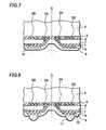
- a BGA type semiconductor device 100 having the semiconductor chip 1is hereby completed. According to the BGA type semiconductor device 100 , only one glass substrate 4 supporting the semiconductor chip 1 is bonded to the semiconductor chip 1 and the glass substrate 4 is processed to reduce its thickness, thus enabling making the whole package thinner. And because the openings 12 are formed in the glass substrate 4 to expose the second wirings 3 B of the semiconductor chip 1 , electrical connections to an external electronic circuit can be made though the openings 12 .
- FIG. 13is a cross-sectional view showing a structure of a stacked MCM as an example of such an electrically connected structure.
- a first semiconductor device 100 a and a second semiconductor device 100 bare stacked in the stacked MCM.
- the first semiconductor device 100 a and the second semiconductor device 100 bhave structures similar to the semiconductor device 100 described above.
- a second wiring 3 B of the first semiconductor device 100 ais electrically and mechanically connected with a conductive terminal 11 B of the second semiconductor device 100 b through an opening 12 . If strength of the connection is not enough, an organic adhesive, such as underfill, may be used supplementary.
- the number of semiconductor devices to be stackedmay be chosen as required.
- the stacked MCMcan be manufactured at reduced cost without using expensive apparatus.
Landscapes
- Engineering & Computer Science (AREA)
- Microelectronics & Electronic Packaging (AREA)
- Power Engineering (AREA)
- Computer Hardware Design (AREA)
- General Physics & Mathematics (AREA)
- Physics & Mathematics (AREA)
- Condensed Matter Physics & Semiconductors (AREA)
- Manufacturing & Machinery (AREA)
- Civil Engineering (AREA)
- Structural Engineering (AREA)
- Internal Circuitry In Semiconductor Integrated Circuit Devices (AREA)
- Dicing (AREA)
- Pressure Sensors (AREA)
Abstract
Description
- This invention is based on Japanese Patent Application No. 2003-120228, the content of which is incorporated by reference in its entirety.[0001]
- 1. Field of the Invention:[0002]
- This invention relates to a semiconductor device and its manufacturing method specifically to a packaging technology of a semiconductor chip.[0003]
- 2. Description of the Related Art:[0004]
- An MCM (Multi-Chip Module) has received attention in recent years as a new packaging technology. The MCM is a high performance module implemented by incorporating a plurality of semiconductor chips into a single package. There are various kinds of MCMs depending on how the semiconductor chips are placed. Among them, attention is focused on a “stacked MCM” which is made by stacking a plurality of semiconductor chips.[0005]
- An example of the stacked MCM structure is shown in FIG. 14. The[0006]
stacked MCM 200 is made by stacking a plurality ofsemiconductor chips 204. Viaholes 205 cutting through thesemiconductor chips 204 are formed by laser processing.Barrier metals 202 are formed on side surfaces of the via holes by sputtering or by CVD (Chemical Vapor Deposition). Verticallyadjacent semiconductor chips 204 are connected with each other through wirings formed by burying conductive material in thevia holes 205 by copper plating. - Insulation between the[0007]
semiconductor chips 204 is maintained by inserting athermoplastic film 203. The plurality ofsemiconductor chips 204 are stacked by repeating such manufacturing process steps. Connections to an external circuit are made throughconductive terminals 206 attached to asemiconductor chip 204 disposed at the bottom of the stack. - The stacked MCM[0008]200 is manufactured by the manufacturing steps described above. The stacked MCM mentioned above is disclosed, for example, in Japanese Patent Application Publication No. 9-232503.
- Manufacturing the stacked[0009]
MCM 200 described above requires forming via holes which are tens of micrometers in diameter and in depth and burying the conductive material in the via holes. Consequently the manufacturing process requires expensive apparatus not used in conventional packaging of semiconductors such as a laser processing machine to process the via holes, barrier CVD equipment to form the barrier metal films and copper plating equipment to bury in the via holes, causing a problem of higher manufacturing cost. - A first wiring and a second wiring are formed on a surface of a semiconductor chip through a first insulation film in a semiconductor device of this invention. A supporting body having an opening to expose the second wiring is bonded to the surface of the semiconductor chip on which the first and the second wirings are formed. A third wiring is formed on a back surface and a side surface of the semiconductor chip through a second insulation film and is connected to the first wiring.[0010]
- FIG. 1 is a cross-sectional view showing a manufacturing method of a semiconductor device according to an embodiment of this invention.[0011]
- FIG. 2 is a cross-sectional view showing the manufacturing method of the semiconductor device according to the embodiment of this invention.[0012]
- FIG. 3 is a cross-sectional view showing the manufacturing method of the semiconductor device according to the embodiment of this invention.[0013]
- FIG. 4 is a cross-sectional view showing the manufacturing method of the semiconductor device according to the embodiment of this invention.[0014]
- FIG. 5 is a cross-sectional view showing the manufacturing method of the semiconductor device according to the embodiment of this invention.[0015]
- FIG. 6 is a cross-sectional view showing the manufacturing method of the semiconductor device according to the embodiment of this invention.[0016]
- FIG. 7 is a cross-sectional view showing the manufacturing method of the semiconductor device according to the embodiment of this invention.[0017]
- FIG. 8 is a cross-sectional view showing the manufacturing method of the semiconductor device according to the embodiment of this invention.[0018]
- FIG. 9 is a cross-sectional view showing the manufacturing method of the semiconductor device according to the embodiment of this invention.[0019]
- FIG. 10 is a cross-sectional view showing the manufacturing method of the semiconductor device according to the embodiment of this invention.[0020]
- FIG. 11 is a cross-sectional view showing the manufacturing method of the semiconductor device according to the embodiment of this invention.[0021]
- FIG. 12 is a cross-sectional view showing the manufacturing method of the semiconductor device according to the embodiment of this invention.[0022]
- FIG. 13 is a cross-sectional view showing the manufacturing method of the semiconductor device according to the embodiment of this invention.[0023]
- FIG. 14 is a diagrammatic drawing showing a cross-section of an MCM type semiconductor device according to a conventional art.[0024]
- Next, a semiconductor device and its manufacturing method according to an embodiment of this invention will be described, referring to FIGS. 1 through 13.[0025]
- First, a[0026]
semiconductor wafer 1ais provided, as shown in FIG. 1. The semiconductor wafer1awill be cut into a plurality ofsemiconductor chips 1 in a process step which will be described later. Thesemiconductor chips 1 are CCD (Charge Coupled Device) image sensors or semiconductor memory chips, for example, and are manufactured by semiconductor wafer processing. A plurality offirst wirings 3A and a plurality ofsecond wirings 3B are formed on a surface of the semiconductor wafer1athrough aninsulation film 2 simultaneously. Thefirst wirings 3A are formed to have a predetermined length of separation from each other across a border S along which the semiconductor wafer1ais to be cut into the plurality ofsemiconductor chips 1. The border S is called a dicing line or a scribe line. - The[0027]
first wiring 3A is to place a pad at a location away from an ordinary bonding pad area on thesemiconductor chip 1 and closer to the border S. The plurality ofsecond wirings 3B connect conductive pads electrically to conductive terminals of another semiconductor device stacked on thesemiconductor chip 1 in a later process step. - Then a[0028]
glass substrate 4 making a supporting body is bonded to the surface of the semiconductor wafer1a,on which thefirst wirings 3A and thesecond wirings 3B are formed, using anepoxy resin layer 5 as an adhesive. Note that a silicon substrate, a plastic plate or a tape- or sheet-shaped material may be used as the supporting body other than the glass substrate used in the embodiment. An adhesive suitable for the chosen supporting body is to be selected in this case. - Next, a surface of the semiconductor wafer[0029]1ato which the
glass substrate 4 is not bonded, i.e., a back surface of thesemiconductor wafer 1a,is back-ground to reduce a thickness of thesemiconductor wafer 1a,as shown in FIG. 2. Scratches arise on the back-ground back surface of the semiconductor wafer1a,causing bumps and dips of several micrometers in width and in depth. Wet etching is conducted to reduce them using a silicon etching solution which has higher selection rate on silicon which is a material for thesilicon wafer 1athan that on silicon dioxide (SiO2) which is a material for theinsulation film 2. A mixed solution composed of 2.5% of hydrofluoric acid, 50% of nitric acid, 10% of acetic acid and 37.5% of water is suitable as the silicon etching solution, for example. - Next, isotropic etching is made on the back surface of the semiconductor wafer[0030]1ausing a mask of photoresist (not shown) provided with an opening along the border S, as shown in FIG. 3. A groove is formed in the
silicon wafer 1aalong the border S to expose theinsulation film 2 partially. Note that the isotropic etching may be performed either by dry-etching or by wet-etching. Although the silicon wafer1ais cut into the plurality ofsemiconductor chips 1 by the etching, it is supported with theglass substrate 4 to maintain a shape of the semiconductor wafer1a. - Bumps and dips, residues and foreign particles are left on the etched back surface of the semiconductor wafer[0031]1a.Also corners are formed as shown in circles a and b depicted with dashed lines in FIG. 3. Wet-etching is conducted to remove the residues and the foreign particles and to round the comers, as shown in FIG. 4. The comers shown in the dashed line circles a and b in FIG. 3 are turned into smooth shapes as shown in dashed line circles a and b in FIG. 4.
- Next, an[0032]
insulation film 7 is formed to cover the back surface and the etched side surface of the plurality ofsemiconductor chips 1, as shown in FIG. 5. Theinsulation film 7 is a silane-based oxide film, for example. - Next, a photoresist film (not shown) is applied to the back surface of the[0033]
semiconductor chip 1 and patterning is made on the photoresist film. Theinsulation film 7 and theinsulation film 2 are etched using the photoresist film as a mask to expose end portions of thefirst wirings 3A. - Next,[0034]
flexible cushioning pads 8 are formed at locations where theconductive terminals 11 are to be formed. Thecushioning pads 8 have function to absorb power applied through theconductive terminals 11 and relax stresses when theconductive terminals 11 are bonded. However this invention does not necessarily require thecushioning pads 8. Then thethird wiring 9 is formed to cover theinsulation film 7, thecushioning pads 8 and the exposed portions of thefirst wirings 3A, as shown in FIG. 6. With this, thefirst wirings 3A are electrically connected with thethird wiring 9. - Next, a photoresist film (not shown) is applied to the back surface of the[0035]
semiconductor chip 1 and pattering is made to form an opening in the photoresist film along the border S. Etching is done using the photoresist film as a mask to remove a portion of thethird wiring 9 around the border S, as shown in FIG. 7. Although not shown in the figure, Ni-Au plating may be applied to a surface of thethird wiring 9 by making electroless plating after forming thethird wiring 9. - Next, a[0036]
protection film 10 is formed over the back surface of thesemiconductor chip 1. A thermosetting organic resin is dropped on the back surface of thesemiconductor chip 1 while the back surface is facing upward, and thesemiconductor wafer 1ahaving the plurality ofsemiconductor chips 1 and bonded to theglass substrate 4 is spun to form theprotection film 10. The organic resin is spread over the surface of thesemiconductor wafer 1aby centrifugal force caused by the spinning. Theprotection film 10 is formed on the surface of thethird wiring 9. - Next, the[0037]
protection film 10 is removed from regions where theconductive terminals 11 are to be formed by selective etching using a photoresist film as a mask to expose thethird wiring 9. Theconductive terminals 11 are formed on the exposedthird wiring 9 to make contact with it, as shown in FIG. 8. Theconductive terminals 11 can be made of projecting electrode terminals such as solder bumps or gold bumps, for example. Thickness of theconductive terminals 11 is 160 μm for solder bumps and can be reduced to several micrometers—tens of micrometers when gold bumps are used. A plurality ofconductive terminals 11 can be formed in similar structure on the back surface of thesemiconductor chip 1 to constitute a BGA (Ball Grid Array). - Next, the[0038]
glass substrate 4 is thinned by removing its surface portion, as shown in FIG. 9. By doing so, processing time to form openings in theglass substrate 4, which will be described later, is shortened. Thickness of 50-100 μm is appropriate for theglass substrate 4. Followings are methods to reduce the thickness of the glass substrate4: (1) grinding theglass substrate 4 with a back-grinding machine; (2) polishing theglass substrate 4 with CMP (Chemical Mechanical Polishing) equipment; (3) etching theglass substrate 4 by dropping etching solution onto theglass substrate 4 and rotating thesemiconductor wafer 1ato which theglass substrate 4 is attached so that the etching solution pervades whole surface of theglass substrate 4, as in photoresist coating; and (4) etching theglass substrate 4 by dry etching. Note that this invention does not necessarily include the process step to reduce the thickness of theglass substrate 4 and that using a supporting body made of plate material shaped in a tape or a sheet having a predetermined thickness from the beginning is not excluded. - Next,[0039]
openings 12 to expose surfaces of thesecond wirings 3B are formed by removing theglass substrate 4 and theresin layer 5 from regions above thesecond wirings 3B by etching, for example, as shown in FIG. 10. Theglass substrate 4 may be thinned after forming theopenings 12. However, processing time to form theopenings 12 becomes longer in this case. Next, aplating layer 13 is formed on each surface of thesecond wirings 3B exposed in theopenings 12. Theplating layer 13 makes a part of thesecond wiring 3B. Theplating layer 13 is formed by stacking a Ni plating layer and a Au plating layer, for example. - Next, the[0040]
semiconductor wafer 1ais cut along the border S and separated into the plurality of semiconductor chips I using a dicing machine, as shown in FIG. 12. Theglass substrate 4, theresin layer 5 and theprotection film 10 are cut along the border S in the process. A BGAtype semiconductor device 100 having thesemiconductor chip 1 is hereby completed. According to the BGAtype semiconductor device 100, only oneglass substrate 4 supporting thesemiconductor chip 1 is bonded to thesemiconductor chip 1 and theglass substrate 4 is processed to reduce its thickness, thus enabling making the whole package thinner. And because theopenings 12 are formed in theglass substrate 4 to expose thesecond wirings 3B of thesemiconductor chip 1, electrical connections to an external electronic circuit can be made though theopenings 12. - FIG. 13 is a cross-sectional view showing a structure of a stacked MCM as an example of such an electrically connected structure. A[0041]
first semiconductor device 100aand asecond semiconductor device 100bare stacked in the stacked MCM. Thefirst semiconductor device 100aand thesecond semiconductor device 100bhave structures similar to thesemiconductor device 100 described above. Asecond wiring 3B of thefirst semiconductor device 100ais electrically and mechanically connected with a conductive terminal11B of thesecond semiconductor device 100bthrough anopening 12. If strength of the connection is not enough, an organic adhesive, such as underfill, may be used supplementary. The number of semiconductor devices to be stacked may be chosen as required. - According to this invention, the stacked MCM can be manufactured at reduced cost without using expensive apparatus.[0042]
Claims (15)
Priority Applications (1)
| Application Number | Priority Date | Filing Date | Title |
|---|---|---|---|
| US11/492,044US7256073B2 (en) | 2003-04-24 | 2006-07-25 | Semiconductor device and manufacturing method thereof |
Applications Claiming Priority (2)
| Application Number | Priority Date | Filing Date | Title |
|---|---|---|---|
| JP2003-120228 | 2003-04-24 | ||
| JP2003120228 | 2003-04-24 |
Related Child Applications (1)
| Application Number | Title | Priority Date | Filing Date |
|---|---|---|---|
| US11/492,044DivisionUS7256073B2 (en) | 2003-04-24 | 2006-07-25 | Semiconductor device and manufacturing method thereof |
Publications (2)
| Publication Number | Publication Date |
|---|---|
| US20040262732A1true US20040262732A1 (en) | 2004-12-30 |
| US7102238B2 US7102238B2 (en) | 2006-09-05 |
Family
ID=32959661
Family Applications (2)
| Application Number | Title | Priority Date | Filing Date |
|---|---|---|---|
| US10/828,556Expired - LifetimeUS7102238B2 (en) | 2003-04-24 | 2004-04-21 | Semiconductor device and manufacturing method thereof |
| US11/492,044Expired - LifetimeUS7256073B2 (en) | 2003-04-24 | 2006-07-25 | Semiconductor device and manufacturing method thereof |
Family Applications After (1)
| Application Number | Title | Priority Date | Filing Date |
|---|---|---|---|
| US11/492,044Expired - LifetimeUS7256073B2 (en) | 2003-04-24 | 2006-07-25 | Semiconductor device and manufacturing method thereof |
Country Status (5)
| Country | Link |
|---|---|
| US (2) | US7102238B2 (en) |
| EP (1) | EP1471571B1 (en) |
| KR (2) | KR20040092435A (en) |
| CN (1) | CN100334723C (en) |
| TW (1) | TWI229890B (en) |
Cited By (15)
| Publication number | Priority date | Publication date | Assignee | Title |
|---|---|---|---|---|
| US20060024949A1 (en)* | 2004-07-29 | 2006-02-02 | Sanyo Electric Co., Ltd. | Method of manufacturing semiconductor device |
| US20060249075A1 (en)* | 2005-03-11 | 2006-11-09 | Kiyonori Oyu | Semiconductor chip with a porous single crystal layer and manufacturing method of the same |
| US20070087524A1 (en)* | 2005-10-18 | 2007-04-19 | Robert Montgomery | Wafer singulation process |
| US20070158806A1 (en)* | 2006-01-12 | 2007-07-12 | Stats Chippac Ltd. | Integrated circuit package system including honeycomb molding |
| US20080157098A1 (en)* | 2006-12-27 | 2008-07-03 | Sanyo Electric Co., Ltd | Semiconductor device and method of manufacturing the same |
| US20080265441A1 (en)* | 2007-04-25 | 2008-10-30 | Sanyo Elelctric Co., Ltd. | Semiconductor device and method of manufacturing the same |
| US20100279504A1 (en)* | 2006-01-12 | 2010-11-04 | Heap Hoe Kuan | Integrated circuit package system including honeycomb molding |
| US20110175223A1 (en)* | 2005-05-19 | 2011-07-21 | Wood Alan G | Stacked Semiconductor Components Having Conductive Interconnects |
| US8581387B1 (en) | 2006-04-24 | 2013-11-12 | Micron Technology, Inc. | Through wire interconnect (TWI) having bonded connection and encapsulating polymer layer |
| US9013044B2 (en) | 2005-12-07 | 2015-04-21 | Micron Technology, Inc. | Through wire interconnect (TWI) for semiconductor components having wire in via and bonded connection with substrate contact |
| CN111446193A (en)* | 2020-03-05 | 2020-07-24 | 绍兴同芯成集成电路有限公司 | Glass carrier plate with central part removed |
| CN111446194A (en)* | 2020-03-05 | 2020-07-24 | 绍兴同芯成集成电路有限公司 | Glass carrier plate for wafer processing |
| CN111599740A (en)* | 2020-04-16 | 2020-08-28 | 绍兴同芯成集成电路有限公司 | Ladder-shaped/gentle slope-shaped wafer bonding glass carrier plate framework |
| CN111599743A (en)* | 2020-07-06 | 2020-08-28 | 绍兴同芯成集成电路有限公司 | Method for producing wafer by combining composite adhesive film with through hole glass carrier plate structure |
| US20220085095A1 (en)* | 2019-02-26 | 2022-03-17 | Hamamatsu Photonics K.K. | Method for manufacturing photodetector, and photodetector |
Families Citing this family (59)
| Publication number | Priority date | Publication date | Assignee | Title |
|---|---|---|---|---|
| TWI232560B (en)* | 2002-04-23 | 2005-05-11 | Sanyo Electric Co | Semiconductor device and its manufacture |
| TWI229435B (en) | 2002-06-18 | 2005-03-11 | Sanyo Electric Co | Manufacture of semiconductor device |
| TWI227550B (en)* | 2002-10-30 | 2005-02-01 | Sanyo Electric Co | Semiconductor device manufacturing method |
| JP4401181B2 (en) | 2003-08-06 | 2010-01-20 | 三洋電機株式会社 | Semiconductor device and manufacturing method thereof |
| US7091124B2 (en) | 2003-11-13 | 2006-08-15 | Micron Technology, Inc. | Methods for forming vias in microelectronic devices, and methods for packaging microelectronic devices |
| US8084866B2 (en) | 2003-12-10 | 2011-12-27 | Micron Technology, Inc. | Microelectronic devices and methods for filling vias in microelectronic devices |
| US20050247894A1 (en) | 2004-05-05 | 2005-11-10 | Watkins Charles M | Systems and methods for forming apertures in microfeature workpieces |
| US7232754B2 (en) | 2004-06-29 | 2007-06-19 | Micron Technology, Inc. | Microelectronic devices and methods for forming interconnects in microelectronic devices |
| US7425499B2 (en) | 2004-08-24 | 2008-09-16 | Micron Technology, Inc. | Methods for forming interconnects in vias and microelectronic workpieces including such interconnects |
| SG120200A1 (en)* | 2004-08-27 | 2006-03-28 | Micron Technology Inc | Slanted vias for electrical circuits on circuit boards and other substrates |
| US7300857B2 (en) | 2004-09-02 | 2007-11-27 | Micron Technology, Inc. | Through-wafer interconnects for photoimager and memory wafers |
| US20060138626A1 (en)* | 2004-12-29 | 2006-06-29 | Tessera, Inc. | Microelectronic packages using a ceramic substrate having a window and a conductive surface region |
| US7271482B2 (en) | 2004-12-30 | 2007-09-18 | Micron Technology, Inc. | Methods for forming interconnects in microelectronic workpieces and microelectronic workpieces formed using such methods |
| TWI313914B (en)* | 2005-01-31 | 2009-08-21 | Sanyo Electric Co | Semiconductor device and a method for manufacturing thereof |
| JP2008541039A (en)* | 2005-05-04 | 2008-11-20 | エヌエックスピー ビー ヴィ | Device comprising a sensor module |
| US7589406B2 (en)* | 2005-06-27 | 2009-09-15 | Micron Technology, Inc. | Stacked semiconductor component |
| US7795134B2 (en) | 2005-06-28 | 2010-09-14 | Micron Technology, Inc. | Conductive interconnect structures and formation methods using supercritical fluids |
| KR100629498B1 (en)* | 2005-07-15 | 2006-09-28 | 삼성전자주식회사 | Micro-Packages, Multi-Stack Micro-Packages, and Methods for Making the Same |
| JP4235835B2 (en)* | 2005-08-08 | 2009-03-11 | セイコーエプソン株式会社 | Semiconductor device |
| US7262134B2 (en) | 2005-09-01 | 2007-08-28 | Micron Technology, Inc. | Microfeature workpieces and methods for forming interconnects in microfeature workpieces |
| US7622377B2 (en)* | 2005-09-01 | 2009-11-24 | Micron Technology, Inc. | Microfeature workpiece substrates having through-substrate vias, and associated methods of formation |
| US7863187B2 (en) | 2005-09-01 | 2011-01-04 | Micron Technology, Inc. | Microfeature workpieces and methods for forming interconnects in microfeature workpieces |
| JP2007165696A (en)* | 2005-12-15 | 2007-06-28 | Sanyo Electric Co Ltd | Semiconductor device and manufacturing method thereof |
| JP5010244B2 (en)* | 2005-12-15 | 2012-08-29 | オンセミコンダクター・トレーディング・リミテッド | Semiconductor device |
| TWI324800B (en) | 2005-12-28 | 2010-05-11 | Sanyo Electric Co | Method for manufacturing semiconductor device |
| US20110267235A1 (en)* | 2006-01-20 | 2011-11-03 | Bae Systems Information And Electronic Systems Integration Inc. | Method of tracking a vehicle using microradios |
| TW200737506A (en)* | 2006-03-07 | 2007-10-01 | Sanyo Electric Co | Semiconductor device and manufacturing method of the same |
| KR100855702B1 (en)* | 2006-04-05 | 2008-09-04 | 엠텍비젼 주식회사 | Wafer Level Package Manufacturing Method |
| US7749899B2 (en) | 2006-06-01 | 2010-07-06 | Micron Technology, Inc. | Microelectronic workpieces and methods and systems for forming interconnects in microelectronic workpieces |
| JP5143382B2 (en)* | 2006-07-27 | 2013-02-13 | オンセミコンダクター・トレーディング・リミテッド | Semiconductor device and manufacturing method thereof |
| JP5258567B2 (en)* | 2006-08-11 | 2013-08-07 | セミコンダクター・コンポーネンツ・インダストリーズ・リミテッド・ライアビリティ・カンパニー | Semiconductor device and manufacturing method thereof |
| US7629249B2 (en) | 2006-08-28 | 2009-12-08 | Micron Technology, Inc. | Microfeature workpieces having conductive interconnect structures formed by chemically reactive processes, and associated systems and methods |
| US7902643B2 (en) | 2006-08-31 | 2011-03-08 | Micron Technology, Inc. | Microfeature workpieces having interconnects and conductive backplanes, and associated systems and methods |
| CN100423249C (en)* | 2006-10-17 | 2008-10-01 | 晶方半导体科技(苏州)有限公司 | "N" Shape Electrically Connected Wafer Level Chip Scale Package Structure and Manufacturing Method |
| CN100423250C (en)* | 2006-10-17 | 2008-10-01 | 晶方半导体科技(苏州)有限公司 | Double-layer lead package structure and manufacturing method thereof |
| US7807508B2 (en) | 2006-10-31 | 2010-10-05 | Tessera Technologies Hungary Kft. | Wafer-level fabrication of lidded chips with electrodeposited dielectric coating |
| US7935568B2 (en) | 2006-10-31 | 2011-05-03 | Tessera Technologies Ireland Limited | Wafer-level fabrication of lidded chips with electrodeposited dielectric coating |
| JP5010247B2 (en)* | 2006-11-20 | 2012-08-29 | オンセミコンダクター・トレーディング・リミテッド | Semiconductor device and manufacturing method thereof |
| US7468544B2 (en)* | 2006-12-07 | 2008-12-23 | Advanced Chip Engineering Technology Inc. | Structure and process for WL-CSP with metal cover |
| US8018071B2 (en)* | 2007-02-07 | 2011-09-13 | Samsung Electronics Co., Ltd. | Stacked structure using semiconductor devices and semiconductor device package including the same |
| JP5301108B2 (en) | 2007-04-20 | 2013-09-25 | セミコンダクター・コンポーネンツ・インダストリーズ・リミテッド・ライアビリティ・カンパニー | Semiconductor device |
| JP5101157B2 (en)* | 2007-05-07 | 2012-12-19 | オンセミコンダクター・トレーディング・リミテッド | Manufacturing method of semiconductor device |
| TW200845339A (en)* | 2007-05-07 | 2008-11-16 | Sanyo Electric Co | Semiconductor device and manufacturing method thereof |
| JP2009032929A (en) | 2007-07-27 | 2009-02-12 | Sanyo Electric Co Ltd | Semiconductor device and manufacturing method thereof |
| JP4548459B2 (en)* | 2007-08-21 | 2010-09-22 | セイコーエプソン株式会社 | Electronic component mounting structure |
| SG150410A1 (en) | 2007-08-31 | 2009-03-30 | Micron Technology Inc | Partitioned through-layer via and associated systems and methods |
| JP5536322B2 (en) | 2007-10-09 | 2014-07-02 | 新光電気工業株式会社 | Substrate manufacturing method |
| TW200924148A (en)* | 2007-11-26 | 2009-06-01 | Ind Tech Res Inst | Structure of three-dimensional stacked dies with vertical electrical self-interconnections and method for manufacturing the same |
| US7884015B2 (en) | 2007-12-06 | 2011-02-08 | Micron Technology, Inc. | Methods for forming interconnects in microelectronic workpieces and microelectronic workpieces formed using such methods |
| US7800238B2 (en)* | 2008-06-27 | 2010-09-21 | Micron Technology, Inc. | Surface depressions for die-to-die interconnects and associated systems and methods |
| JP2010103300A (en)* | 2008-10-23 | 2010-05-06 | Sanyo Electric Co Ltd | Semiconductor device, and method of manufacturing the same |
| US8298917B2 (en)* | 2009-04-14 | 2012-10-30 | International Business Machines Corporation | Process for wet singulation using a dicing singulation structure |
| JP2012039005A (en)* | 2010-08-10 | 2012-02-23 | Toshiba Corp | Semiconductor device and method of manufacturing the same |
| DE102011112659B4 (en)* | 2011-09-06 | 2022-01-27 | Vishay Semiconductor Gmbh | Surface mount electronic component |
| KR102492366B1 (en)* | 2015-09-15 | 2023-01-27 | 닛산 가가쿠 가부시키가이샤 | Surface roughening method by wet treatment |
| CN110498386B (en)* | 2019-08-29 | 2022-09-27 | 深迪半导体(绍兴)有限公司 | Semiconductor chip and processing method thereof |
| CN111446192A (en)* | 2020-03-05 | 2020-07-24 | 绍兴同芯成集成电路有限公司 | Glass carrier plate with groove-shaped window hole |
| CN111524820B (en)* | 2020-04-29 | 2021-08-31 | 绍兴同芯成集成电路有限公司 | Wafer double-sided lead-tin alloy bump forming process |
| CN111430325A (en)* | 2020-04-29 | 2020-07-17 | 绍兴同芯成集成电路有限公司 | Process structure of wafer double-sided alloy bump |
Citations (7)
| Publication number | Priority date | Publication date | Assignee | Title |
|---|---|---|---|---|
| US5648684A (en)* | 1995-07-26 | 1997-07-15 | International Business Machines Corporation | Endcap chip with conductive, monolithic L-connect for multichip stack |
| US6002163A (en)* | 1998-01-02 | 1999-12-14 | General Electric Company | Electronic device pad relocation, precision placement, and packaging in arrays |
| US6054760A (en)* | 1996-12-23 | 2000-04-25 | Scb Technologies Inc. | Surface-connectable semiconductor bridge elements and devices including the same |
| US6221751B1 (en)* | 1997-01-24 | 2001-04-24 | Chipscale, Inc. | Wafer fabrication of die-bottom contacts for electronic devices |
| US6326689B1 (en)* | 1999-07-26 | 2001-12-04 | Stmicroelectronics, Inc. | Backside contact for touchchip |
| US20020139577A1 (en)* | 2001-03-27 | 2002-10-03 | Miller Charles A. | In-street integrated circuit wafer via |
| US6894386B2 (en)* | 2001-10-08 | 2005-05-17 | Micron Technology, Inc. | Apparatus and method for packaging circuits |
Family Cites Families (6)
| Publication number | Priority date | Publication date | Assignee | Title |
|---|---|---|---|---|
| JP3610661B2 (en) | 1996-02-21 | 2005-01-19 | 株式会社日立製作所 | Three-dimensional laminated module |
| JP3437369B2 (en)* | 1996-03-19 | 2003-08-18 | 松下電器産業株式会社 | Chip carrier and semiconductor device using the same |
| JP4329235B2 (en) | 2000-06-27 | 2009-09-09 | セイコーエプソン株式会社 | Semiconductor device and manufacturing method thereof |
| JP2002093942A (en)* | 2000-09-14 | 2002-03-29 | Nec Corp | Semiconductor device and its manufacturing method |
| JP3433193B2 (en)* | 2000-10-23 | 2003-08-04 | 松下電器産業株式会社 | Semiconductor chip and manufacturing method thereof |
| US6693358B2 (en) | 2000-10-23 | 2004-02-17 | Matsushita Electric Industrial Co., Ltd. | Semiconductor chip, wiring board and manufacturing process thereof as well as semiconductor device |
- 2004
- 2004-04-07TWTW093109555Apatent/TWI229890B/ennot_activeIP Right Cessation
- 2004-04-21KRKR1020040027385Apatent/KR20040092435A/ennot_activeCeased
- 2004-04-21USUS10/828,556patent/US7102238B2/ennot_activeExpired - Lifetime
- 2004-04-26CNCNB2004100384578Apatent/CN100334723C/ennot_activeExpired - Fee Related
- 2004-04-26EPEP04009853.5Apatent/EP1471571B1/ennot_activeExpired - Lifetime
- 2006
- 2006-06-29KRKR1020060059179Apatent/KR100938970B1/ennot_activeExpired - Fee Related
- 2006-07-25USUS11/492,044patent/US7256073B2/ennot_activeExpired - Lifetime
Patent Citations (7)
| Publication number | Priority date | Publication date | Assignee | Title |
|---|---|---|---|---|
| US5648684A (en)* | 1995-07-26 | 1997-07-15 | International Business Machines Corporation | Endcap chip with conductive, monolithic L-connect for multichip stack |
| US6054760A (en)* | 1996-12-23 | 2000-04-25 | Scb Technologies Inc. | Surface-connectable semiconductor bridge elements and devices including the same |
| US6221751B1 (en)* | 1997-01-24 | 2001-04-24 | Chipscale, Inc. | Wafer fabrication of die-bottom contacts for electronic devices |
| US6002163A (en)* | 1998-01-02 | 1999-12-14 | General Electric Company | Electronic device pad relocation, precision placement, and packaging in arrays |
| US6326689B1 (en)* | 1999-07-26 | 2001-12-04 | Stmicroelectronics, Inc. | Backside contact for touchchip |
| US20020139577A1 (en)* | 2001-03-27 | 2002-10-03 | Miller Charles A. | In-street integrated circuit wafer via |
| US6894386B2 (en)* | 2001-10-08 | 2005-05-17 | Micron Technology, Inc. | Apparatus and method for packaging circuits |
Cited By (27)
| Publication number | Priority date | Publication date | Assignee | Title |
|---|---|---|---|---|
| US20060024949A1 (en)* | 2004-07-29 | 2006-02-02 | Sanyo Electric Co., Ltd. | Method of manufacturing semiconductor device |
| US7557017B2 (en)* | 2004-07-29 | 2009-07-07 | Sanyo Electric Co., Ltd. | Method of manufacturing semiconductor device with two-step etching of layer |
| US20060249075A1 (en)* | 2005-03-11 | 2006-11-09 | Kiyonori Oyu | Semiconductor chip with a porous single crystal layer and manufacturing method of the same |
| US7632696B2 (en)* | 2005-03-11 | 2009-12-15 | Elpida Memory, Inc. | Semiconductor chip with a porous single crystal layer and manufacturing method of the same |
| US8546931B2 (en)* | 2005-05-19 | 2013-10-01 | Micron Technology, Inc. | Stacked semiconductor components having conductive interconnects |
| US20110175223A1 (en)* | 2005-05-19 | 2011-07-21 | Wood Alan G | Stacked Semiconductor Components Having Conductive Interconnects |
| US20070087524A1 (en)* | 2005-10-18 | 2007-04-19 | Robert Montgomery | Wafer singulation process |
| US8153464B2 (en)* | 2005-10-18 | 2012-04-10 | International Rectifier Corporation | Wafer singulation process |
| US9013044B2 (en) | 2005-12-07 | 2015-04-21 | Micron Technology, Inc. | Through wire interconnect (TWI) for semiconductor components having wire in via and bonded connection with substrate contact |
| US20070158806A1 (en)* | 2006-01-12 | 2007-07-12 | Stats Chippac Ltd. | Integrated circuit package system including honeycomb molding |
| US7737539B2 (en)* | 2006-01-12 | 2010-06-15 | Stats Chippac Ltd. | Integrated circuit package system including honeycomb molding |
| US8217501B2 (en) | 2006-01-12 | 2012-07-10 | Stats Chippac Ltd. | Integrated circuit package system including honeycomb molding |
| US20100237488A1 (en)* | 2006-01-12 | 2010-09-23 | Hyeog Chan Kwon | Integrated circuit package system including honeycomb molding |
| US20100279504A1 (en)* | 2006-01-12 | 2010-11-04 | Heap Hoe Kuan | Integrated circuit package system including honeycomb molding |
| US8409921B2 (en) | 2006-01-12 | 2013-04-02 | Stats Chippac Ltd. | Integrated circuit package system including honeycomb molding |
| US8581387B1 (en) | 2006-04-24 | 2013-11-12 | Micron Technology, Inc. | Through wire interconnect (TWI) having bonded connection and encapsulating polymer layer |
| US8741667B2 (en) | 2006-04-24 | 2014-06-03 | Micron Technology, Inc. | Method for fabricating a through wire interconnect (TWI) on a semiconductor substrate having a bonded connection and an encapsulating polymer layer |
| US9018751B2 (en) | 2006-04-24 | 2015-04-28 | Micron Technology, Inc. | Semiconductor module system having encapsulated through wire interconnect (TWI) |
| US7847299B2 (en)* | 2006-12-27 | 2010-12-07 | Sanyo Electric Co., Ltd. | Semiconductor device and method of manufacturing the same |
| US20080157098A1 (en)* | 2006-12-27 | 2008-07-03 | Sanyo Electric Co., Ltd | Semiconductor device and method of manufacturing the same |
| US7759779B2 (en)* | 2007-04-25 | 2010-07-20 | Sanyo Semiconductor Co., Ltd. | Semiconductor device and method of manufacturing the same |
| US20080265441A1 (en)* | 2007-04-25 | 2008-10-30 | Sanyo Elelctric Co., Ltd. | Semiconductor device and method of manufacturing the same |
| US20220085095A1 (en)* | 2019-02-26 | 2022-03-17 | Hamamatsu Photonics K.K. | Method for manufacturing photodetector, and photodetector |
| CN111446193A (en)* | 2020-03-05 | 2020-07-24 | 绍兴同芯成集成电路有限公司 | Glass carrier plate with central part removed |
| CN111446194A (en)* | 2020-03-05 | 2020-07-24 | 绍兴同芯成集成电路有限公司 | Glass carrier plate for wafer processing |
| CN111599740A (en)* | 2020-04-16 | 2020-08-28 | 绍兴同芯成集成电路有限公司 | Ladder-shaped/gentle slope-shaped wafer bonding glass carrier plate framework |
| CN111599743A (en)* | 2020-07-06 | 2020-08-28 | 绍兴同芯成集成电路有限公司 | Method for producing wafer by combining composite adhesive film with through hole glass carrier plate structure |
Also Published As
| Publication number | Publication date |
|---|---|
| TWI229890B (en) | 2005-03-21 |
| EP1471571B1 (en) | 2013-09-04 |
| EP1471571A1 (en) | 2004-10-27 |
| CN1551347A (en) | 2004-12-01 |
| KR20060088518A (en) | 2006-08-04 |
| KR100938970B1 (en) | 2010-01-26 |
| US7256073B2 (en) | 2007-08-14 |
| US20060270093A1 (en) | 2006-11-30 |
| KR20040092435A (en) | 2004-11-03 |
| US7102238B2 (en) | 2006-09-05 |
| CN100334723C (en) | 2007-08-29 |
| TW200425245A (en) | 2004-11-16 |
Similar Documents
| Publication | Publication Date | Title |
|---|---|---|
| US7256073B2 (en) | Semiconductor device and manufacturing method thereof | |
| US11456251B2 (en) | Semiconductor structure, package structure, and manufacturing method thereof | |
| US7919875B2 (en) | Semiconductor device with recess portion over pad electrode | |
| US11749651B2 (en) | Semiconductor package and manufacturing method thereof | |
| US7981807B2 (en) | Manufacturing method of semiconductor device with smoothing | |
| US7271466B2 (en) | Semiconductor device with sidewall wiring | |
| US20090261476A1 (en) | Semiconductor device and manufacturing method thereof | |
| KR101245928B1 (en) | Ultra-thin stacked chips packaging | |
| JP4100936B2 (en) | Manufacturing method of semiconductor device | |
| KR100565961B1 (en) | 3D stacked chip package manufacturing method | |
| JP3602118B2 (en) | Semiconductor device | |
| WO2002101831A1 (en) | Semiconductor device and its manufacturing method | |
| CN100592513C (en) | Chip component and method for manufacturing chip component | |
| US20220293483A1 (en) | Semiconductor package and method of fabricating the same | |
| EP1478021A1 (en) | Semiconductor device and manufacturing method thereof | |
| JP4334397B2 (en) | Semiconductor device and manufacturing method thereof | |
| CN117690804A (en) | Wafer level packaging method | |
| CN120109113A (en) | Semiconductor package and method of manufacturing semiconductor package | |
| JP2010087295A (en) | Semiconductor chip and method of manufacturing the same and semiconductor device and method of manufacturing the same |
Legal Events
| Date | Code | Title | Description |
|---|---|---|---|
| AS | Assignment | Owner name:SANYO ELECTRIC CO., LTD., JAPAN Free format text:ASSIGNMENT OF ASSIGNORS INTEREST;ASSIGNORS:NOMA, TAKASHI;SUZUKI, AKIRA;SHINOGI, HIROYUKI;REEL/FRAME:015752/0021;SIGNING DATES FROM 20040729 TO 20040730 | |
| STCF | Information on status: patent grant | Free format text:PATENTED CASE | |
| FEPP | Fee payment procedure | Free format text:PAYOR NUMBER ASSIGNED (ORIGINAL EVENT CODE: ASPN); ENTITY STATUS OF PATENT OWNER: LARGE ENTITY | |
| FPAY | Fee payment | Year of fee payment:4 | |
| FEPP | Fee payment procedure | Free format text:PAYOR NUMBER ASSIGNED (ORIGINAL EVENT CODE: ASPN); ENTITY STATUS OF PATENT OWNER: LARGE ENTITY | |
| AS | Assignment | Owner name:SEMICONDUCTOR COMPONENTS INDUSTRIES, LLC, ARIZONA Free format text:ASSIGNMENT OF ASSIGNORS INTEREST;ASSIGNOR:SANYO ELECTRIC CO., LTD.;REEL/FRAME:026594/0385 Effective date:20110101 | |
| FPAY | Fee payment | Year of fee payment:8 | |
| AS | Assignment | Owner name:SEMICONDUCTOR COMPONENTS INDUSTRIES, LLC, ARIZONA Free format text:CORRECTIVE ASSIGNMENT TO CORRECT THE INCORRECT #12/577882 PREVIOUSLY RECORDED ON REEL 026594 FRAME 0385. ASSIGNOR(S) HEREBY CONFIRMS THE ASSIGNMENT;ASSIGNOR:SANYO ELECTRIC CO., LTD;REEL/FRAME:032836/0342 Effective date:20110101 | |
| AS | Assignment | Owner name:DEUTSCHE BANK AG NEW YORK BRANCH, NEW YORK Free format text:SECURITY INTEREST;ASSIGNOR:SEMICONDUCTOR COMPONENTS INDUSTRIES, LLC;REEL/FRAME:038620/0087 Effective date:20160415 | |
| AS | Assignment | Owner name:DEUTSCHE BANK AG NEW YORK BRANCH, AS COLLATERAL AGENT, NEW YORK Free format text:CORRECTIVE ASSIGNMENT TO CORRECT THE INCORRECT PATENT NUMBER 5859768 AND TO RECITE COLLATERAL AGENT ROLE OF RECEIVING PARTY IN THE SECURITY INTEREST PREVIOUSLY RECORDED ON REEL 038620 FRAME 0087. ASSIGNOR(S) HEREBY CONFIRMS THE SECURITY INTEREST;ASSIGNOR:SEMICONDUCTOR COMPONENTS INDUSTRIES, LLC;REEL/FRAME:039853/0001 Effective date:20160415 Owner name:DEUTSCHE BANK AG NEW YORK BRANCH, AS COLLATERAL AG Free format text:CORRECTIVE ASSIGNMENT TO CORRECT THE INCORRECT PATENT NUMBER 5859768 AND TO RECITE COLLATERAL AGENT ROLE OF RECEIVING PARTY IN THE SECURITY INTEREST PREVIOUSLY RECORDED ON REEL 038620 FRAME 0087. ASSIGNOR(S) HEREBY CONFIRMS THE SECURITY INTEREST;ASSIGNOR:SEMICONDUCTOR COMPONENTS INDUSTRIES, LLC;REEL/FRAME:039853/0001 Effective date:20160415 | |
| MAFP | Maintenance fee payment | Free format text:PAYMENT OF MAINTENANCE FEE, 12TH YEAR, LARGE ENTITY (ORIGINAL EVENT CODE: M1553) Year of fee payment:12 | |
| AS | Assignment | Owner name:FAIRCHILD SEMICONDUCTOR CORPORATION, ARIZONA Free format text:RELEASE OF SECURITY INTEREST IN PATENTS RECORDED AT REEL 038620, FRAME 0087;ASSIGNOR:DEUTSCHE BANK AG NEW YORK BRANCH, AS COLLATERAL AGENT;REEL/FRAME:064070/0001 Effective date:20230622 Owner name:SEMICONDUCTOR COMPONENTS INDUSTRIES, LLC, ARIZONA Free format text:RELEASE OF SECURITY INTEREST IN PATENTS RECORDED AT REEL 038620, FRAME 0087;ASSIGNOR:DEUTSCHE BANK AG NEW YORK BRANCH, AS COLLATERAL AGENT;REEL/FRAME:064070/0001 Effective date:20230622 |