US20040256662A1 - Nonvolatile memory device using semiconductor nanocrystals and method of forming same - Google Patents
Nonvolatile memory device using semiconductor nanocrystals and method of forming sameDownload PDFInfo
- Publication number
- US20040256662A1 US20040256662A1US10/465,797US46579703AUS2004256662A1US 20040256662 A1US20040256662 A1US 20040256662A1US 46579703 AUS46579703 AUS 46579703AUS 2004256662 A1US2004256662 A1US 2004256662A1
- Authority
- US
- United States
- Prior art keywords
- nanoparticles
- floating gate
- field effect
- effect transistor
- silicon
- Prior art date
- Legal status (The legal status is an assumption and is not a legal conclusion. Google has not performed a legal analysis and makes no representation as to the accuracy of the status listed.)
- Granted
Links
- 238000000034methodMethods0.000titleclaimsabstractdescription69
- 239000004054semiconductor nanocrystalSubstances0.000title1
- 239000002105nanoparticleSubstances0.000claimsabstractdescription70
- 239000000463materialSubstances0.000claimsabstractdescription57
- 238000007667floatingMethods0.000claimsabstractdescription51
- 230000005669field effectEffects0.000claimsabstractdescription22
- 239000002159nanocrystalSubstances0.000claimsdescription101
- XUIMIQQOPSSXEZ-UHFFFAOYSA-NSiliconChemical compound[Si]XUIMIQQOPSSXEZ-UHFFFAOYSA-N0.000claimsdescription63
- 229910052710siliconInorganic materials0.000claimsdescription56
- 239000010703siliconSubstances0.000claimsdescription56
- 239000010408filmSubstances0.000claimsdescription42
- 229920003229poly(methyl methacrylate)Polymers0.000claimsdescription35
- 239000004926polymethyl methacrylateSubstances0.000claimsdescription35
- 238000001338self-assemblyMethods0.000claimsdescription28
- 230000008569processEffects0.000claimsdescription27
- 229920000359diblock copolymerPolymers0.000claimsdescription26
- 229920000642polymerPolymers0.000claimsdescription26
- 239000004793PolystyreneSubstances0.000claimsdescription22
- 238000009826distributionMethods0.000claimsdescription21
- 239000002245particleSubstances0.000claimsdescription21
- 239000011148porous materialSubstances0.000claimsdescription20
- 229920002223polystyrenePolymers0.000claimsdescription18
- 229920002717polyvinylpyridinePolymers0.000claimsdescription16
- 239000000758substrateSubstances0.000claimsdescription15
- 239000010409thin filmSubstances0.000claimsdescription14
- 238000000151depositionMethods0.000claimsdescription12
- 238000005530etchingMethods0.000claimsdescription11
- 229920006254polymer filmPolymers0.000claimsdescription11
- 229920001400block copolymerPolymers0.000claimsdescription9
- 238000004519manufacturing processMethods0.000claimsdescription8
- 229910000577Silicon-germaniumInorganic materials0.000claimsdescription6
- 229910021417amorphous siliconInorganic materials0.000claimsdescription6
- 229910052732germaniumInorganic materials0.000claimsdescription6
- GNPVGFCGXDBREM-UHFFFAOYSA-Ngermanium atomChemical compound[Ge]GNPVGFCGXDBREM-UHFFFAOYSA-N0.000claimsdescription6
- 229920001485poly(butyl acrylate) polymerPolymers0.000claimsdescription6
- 229920001490poly(butyl methacrylate) polymerPolymers0.000claimsdescription6
- -1poly(methyl methacrylate)Polymers0.000claimsdescription6
- LEVVHYCKPQWKOP-UHFFFAOYSA-N[Si].[Ge]Chemical compound[Si].[Ge]LEVVHYCKPQWKOP-UHFFFAOYSA-N0.000claimsdescription5
- 239000002184metalSubstances0.000claimsdescription5
- 229910052751metalInorganic materials0.000claimsdescription5
- 239000004065semiconductorSubstances0.000claimsdescription5
- 239000005062PolybutadieneSubstances0.000claimsdescription4
- 239000012777electrically insulating materialSubstances0.000claimsdescription4
- 229920002857polybutadienePolymers0.000claimsdescription4
- 229920001195polyisoprenePolymers0.000claimsdescription4
- 239000004020conductorSubstances0.000claimsdescription3
- 230000003362replicative effectEffects0.000claimsdescription3
- 239000004205dimethyl polysiloxaneSubstances0.000claimsdescription2
- 239000011810insulating materialSubstances0.000claimsdescription2
- 239000005543nano-size silicon particleSubstances0.000claimsdescription2
- 230000003647oxidationEffects0.000claimsdescription2
- 238000007254oxidation reactionMethods0.000claimsdescription2
- 229920000435poly(dimethylsiloxane)Polymers0.000claimsdescription2
- 230000002542deteriorative effectEffects0.000claims1
- 125000006850spacer groupChemical group0.000claims1
- 230000015654memoryEffects0.000description19
- 239000010410layerSubstances0.000description17
- 238000001020plasma etchingMethods0.000description14
- VYPSYNLAJGMNEJ-UHFFFAOYSA-NSilicium dioxideChemical compoundO=[Si]=OVYPSYNLAJGMNEJ-UHFFFAOYSA-N0.000description10
- 230000008901benefitEffects0.000description10
- 229920000390Poly(styrene-block-methyl methacrylate)Polymers0.000description9
- 230000000694effectsEffects0.000description7
- 238000005229chemical vapour depositionMethods0.000description6
- 238000007796conventional methodMethods0.000description6
- 238000003860storageMethods0.000description6
- 238000003491arrayMethods0.000description5
- 230000015572biosynthetic processEffects0.000description5
- 238000007600chargingMethods0.000description5
- 150000004767nitridesChemical class0.000description5
- 238000000231atomic layer depositionMethods0.000description4
- 229910052681coesiteInorganic materials0.000description4
- 229910052906cristobaliteInorganic materials0.000description4
- 230000008021depositionEffects0.000description4
- 238000010586diagramMethods0.000description4
- 239000003989dielectric materialSubstances0.000description4
- 238000000059patterningMethods0.000description4
- 239000000377silicon dioxideSubstances0.000description4
- 229910052682stishoviteInorganic materials0.000description4
- 238000012546transferMethods0.000description4
- 229910052905tridymiteInorganic materials0.000description4
- QTBSBXVTEAMEQO-UHFFFAOYSA-NAcetic acidChemical compoundCC(O)=OQTBSBXVTEAMEQO-UHFFFAOYSA-N0.000description3
- KRHYYFGTRYWZRS-UHFFFAOYSA-NFluoraneChemical compoundFKRHYYFGTRYWZRS-UHFFFAOYSA-N0.000description3
- YXFVVABEGXRONW-UHFFFAOYSA-NTolueneChemical compoundCC1=CC=CC=C1YXFVVABEGXRONW-UHFFFAOYSA-N0.000description3
- 230000014759maintenance of locationEffects0.000description3
- 229910021420polycrystalline siliconInorganic materials0.000description3
- 238000001878scanning electron micrographMethods0.000description3
- XKRFYHLGVUSROY-UHFFFAOYSA-NArgonChemical compound[Ar]XKRFYHLGVUSROY-UHFFFAOYSA-N0.000description2
- PNEYBMLMFCGWSK-UHFFFAOYSA-Naluminium oxideInorganic materials[O-2].[O-2].[O-2].[Al+3].[Al+3]PNEYBMLMFCGWSK-UHFFFAOYSA-N0.000description2
- 230000008878couplingEffects0.000description2
- 238000010168coupling processMethods0.000description2
- 238000005859coupling reactionMethods0.000description2
- 238000005516engineering processMethods0.000description2
- 150000002500ionsChemical class0.000description2
- 238000004518low pressure chemical vapour depositionMethods0.000description2
- 239000011159matrix materialSubstances0.000description2
- 230000007246mechanismEffects0.000description2
- 238000012856packingMethods0.000description2
- 238000000623plasma-assisted chemical vapour depositionMethods0.000description2
- 229920005591polysiliconPolymers0.000description2
- 102000004169proteins and genesHuman genes0.000description2
- 108090000623proteins and genesProteins0.000description2
- 238000001289rapid thermal chemical vapour depositionMethods0.000description2
- 239000013545self-assembled monolayerSubstances0.000description2
- 229910052814silicon oxideInorganic materials0.000description2
- 239000000126substanceSubstances0.000description2
- 238000012876topographyMethods0.000description2
- 230000005641tunnelingEffects0.000description2
- 208000000044AmnesiaDiseases0.000description1
- XPDWGBQVDMORPB-UHFFFAOYSA-NFluoroformChemical compoundFC(F)FXPDWGBQVDMORPB-UHFFFAOYSA-N0.000description1
- 229910052581Si3N4Inorganic materials0.000description1
- 238000000137annealingMethods0.000description1
- 229910052786argonInorganic materials0.000description1
- 230000006399behaviorEffects0.000description1
- 238000004364calculation methodMethods0.000description1
- 230000001413cellular effectEffects0.000description1
- 238000011109contaminationMethods0.000description1
- 229920001577copolymerPolymers0.000description1
- 239000013078crystalSubstances0.000description1
- 238000005137deposition processMethods0.000description1
- 238000009792diffusion processMethods0.000description1
- 238000007786electrostatic chargingMethods0.000description1
- 239000007943implantSubstances0.000description1
- 238000001459lithographyMethods0.000description1
- 231100000863loss of memoryToxicity0.000description1
- 239000000203mixtureSubstances0.000description1
- 230000004048modificationEffects0.000description1
- 238000012986modificationMethods0.000description1
- QPJSUIGXIBEQAC-UHFFFAOYSA-Nn-(2,4-dichloro-5-propan-2-yloxyphenyl)acetamideChemical compoundCC(C)OC1=CC(NC(C)=O)=C(Cl)C=C1ClQPJSUIGXIBEQAC-UHFFFAOYSA-N0.000description1
- 230000006911nucleationEffects0.000description1
- 238000010899nucleationMethods0.000description1
- 230000001590oxidative effectEffects0.000description1
- 230000037361pathwayEffects0.000description1
- 238000005325percolationMethods0.000description1
- 239000002096quantum dotSubstances0.000description1
- 238000011160researchMethods0.000description1
- 230000000717retained effectEffects0.000description1
- 238000000926separation methodMethods0.000description1
- HQVNEWCFYHHQES-UHFFFAOYSA-Nsilicon nitrideChemical compoundN12[Si]34N5[Si]62N3[Si]51N64HQVNEWCFYHHQES-UHFFFAOYSA-N0.000description1
- 239000002210silicon-based materialSubstances0.000description1
- 239000011856silicon-based particleSubstances0.000description1
- 238000004513sizingMethods0.000description1
- 239000002904solventSubstances0.000description1
- 238000004381surface treatmentMethods0.000description1
- 238000003631wet chemical etchingMethods0.000description1
Images


Classifications
- B—PERFORMING OPERATIONS; TRANSPORTING
- B82—NANOTECHNOLOGY
- B82Y—SPECIFIC USES OR APPLICATIONS OF NANOSTRUCTURES; MEASUREMENT OR ANALYSIS OF NANOSTRUCTURES; MANUFACTURE OR TREATMENT OF NANOSTRUCTURES
- B82Y10/00—Nanotechnology for information processing, storage or transmission, e.g. quantum computing or single electron logic
- H—ELECTRICITY
- H10—SEMICONDUCTOR DEVICES; ELECTRIC SOLID-STATE DEVICES NOT OTHERWISE PROVIDED FOR
- H10D—INORGANIC ELECTRIC SEMICONDUCTOR DEVICES
- H10D30/00—Field-effect transistors [FET]
- H10D30/01—Manufacture or treatment
- H10D30/021—Manufacture or treatment of FETs having insulated gates [IGFET]
- H10D30/0411—Manufacture or treatment of FETs having insulated gates [IGFET] of FETs having floating gates
- H—ELECTRICITY
- H01—ELECTRIC ELEMENTS
- H01L—SEMICONDUCTOR DEVICES NOT COVERED BY CLASS H10
- H01L21/00—Processes or apparatus adapted for the manufacture or treatment of semiconductor or solid state devices or of parts thereof
- H01L21/02—Manufacture or treatment of semiconductor devices or of parts thereof
- H01L21/02104—Forming layers
- H01L21/02107—Forming insulating materials on a substrate
- H01L21/02109—Forming insulating materials on a substrate characterised by the type of layer, e.g. type of material, porous/non-porous, pre-cursors, mixtures or laminates
- H01L21/02112—Forming insulating materials on a substrate characterised by the type of layer, e.g. type of material, porous/non-porous, pre-cursors, mixtures or laminates characterised by the material of the layer
- H01L21/02118—Forming insulating materials on a substrate characterised by the type of layer, e.g. type of material, porous/non-porous, pre-cursors, mixtures or laminates characterised by the material of the layer carbon based polymeric organic or inorganic material, e.g. polyimides, poly cyclobutene or PVC
- H—ELECTRICITY
- H01—ELECTRIC ELEMENTS
- H01L—SEMICONDUCTOR DEVICES NOT COVERED BY CLASS H10
- H01L21/00—Processes or apparatus adapted for the manufacture or treatment of semiconductor or solid state devices or of parts thereof
- H01L21/02—Manufacture or treatment of semiconductor devices or of parts thereof
- H01L21/02104—Forming layers
- H01L21/02107—Forming insulating materials on a substrate
- H01L21/02225—Forming insulating materials on a substrate characterised by the process for the formation of the insulating layer
- H01L21/02227—Forming insulating materials on a substrate characterised by the process for the formation of the insulating layer formation by a process other than a deposition process
- H—ELECTRICITY
- H01—ELECTRIC ELEMENTS
- H01L—SEMICONDUCTOR DEVICES NOT COVERED BY CLASS H10
- H01L21/00—Processes or apparatus adapted for the manufacture or treatment of semiconductor or solid state devices or of parts thereof
- H01L21/02—Manufacture or treatment of semiconductor devices or of parts thereof
- H01L21/02104—Forming layers
- H01L21/02365—Forming inorganic semiconducting materials on a substrate
- H01L21/02518—Deposited layers
- H01L21/02521—Materials
- H01L21/02524—Group 14 semiconducting materials
- H01L21/02532—Silicon, silicon germanium, germanium
- H—ELECTRICITY
- H01—ELECTRIC ELEMENTS
- H01L—SEMICONDUCTOR DEVICES NOT COVERED BY CLASS H10
- H01L21/00—Processes or apparatus adapted for the manufacture or treatment of semiconductor or solid state devices or of parts thereof
- H01L21/02—Manufacture or treatment of semiconductor devices or of parts thereof
- H01L21/02104—Forming layers
- H01L21/02365—Forming inorganic semiconducting materials on a substrate
- H01L21/02612—Formation types
- H01L21/02617—Deposition types
- H01L21/02636—Selective deposition, e.g. simultaneous growth of mono- and non-monocrystalline semiconductor materials
- H—ELECTRICITY
- H01—ELECTRIC ELEMENTS
- H01L—SEMICONDUCTOR DEVICES NOT COVERED BY CLASS H10
- H01L21/00—Processes or apparatus adapted for the manufacture or treatment of semiconductor or solid state devices or of parts thereof
- H01L21/02—Manufacture or treatment of semiconductor devices or of parts thereof
- H01L21/04—Manufacture or treatment of semiconductor devices or of parts thereof the devices having potential barriers, e.g. a PN junction, depletion layer or carrier concentration layer
- H01L21/18—Manufacture or treatment of semiconductor devices or of parts thereof the devices having potential barriers, e.g. a PN junction, depletion layer or carrier concentration layer the devices having semiconductor bodies comprising elements of Group IV of the Periodic Table or AIIIBV compounds with or without impurities, e.g. doping materials
- H01L21/30—Treatment of semiconductor bodies using processes or apparatus not provided for in groups H01L21/20 - H01L21/26
- H01L21/31—Treatment of semiconductor bodies using processes or apparatus not provided for in groups H01L21/20 - H01L21/26 to form insulating layers thereon, e.g. for masking or by using photolithographic techniques; After treatment of these layers; Selection of materials for these layers
- H01L21/3105—After-treatment
- H01L21/311—Etching the insulating layers by chemical or physical means
- H01L21/31105—Etching inorganic layers
- H01L21/31111—Etching inorganic layers by chemical means
- H—ELECTRICITY
- H10—SEMICONDUCTOR DEVICES; ELECTRIC SOLID-STATE DEVICES NOT OTHERWISE PROVIDED FOR
- H10D—INORGANIC ELECTRIC SEMICONDUCTOR DEVICES
- H10D30/00—Field-effect transistors [FET]
- H10D30/60—Insulated-gate field-effect transistors [IGFET]
- H10D30/68—Floating-gate IGFETs
- H10D30/687—Floating-gate IGFETs having more than two programming levels
- H—ELECTRICITY
- H10—SEMICONDUCTOR DEVICES; ELECTRIC SOLID-STATE DEVICES NOT OTHERWISE PROVIDED FOR
- H10D—INORGANIC ELECTRIC SEMICONDUCTOR DEVICES
- H10D30/00—Field-effect transistors [FET]
- H10D30/60—Insulated-gate field-effect transistors [IGFET]
- H10D30/68—Floating-gate IGFETs
- H10D30/6891—Floating-gate IGFETs characterised by the shapes, relative sizes or dispositions of the floating gate electrode
- H10D30/6893—Floating-gate IGFETs characterised by the shapes, relative sizes or dispositions of the floating gate electrode wherein the floating gate has multiple non-connected parts, e.g. multi-particle floating gate
- H—ELECTRICITY
- H10—SEMICONDUCTOR DEVICES; ELECTRIC SOLID-STATE DEVICES NOT OTHERWISE PROVIDED FOR
- H10D—INORGANIC ELECTRIC SEMICONDUCTOR DEVICES
- H10D30/00—Field-effect transistors [FET]
- H10D30/60—Insulated-gate field-effect transistors [IGFET]
- H10D30/69—IGFETs having charge trapping gate insulators, e.g. MNOS transistors
- H10D30/691—IGFETs having charge trapping gate insulators, e.g. MNOS transistors having more than two programming levels
- H—ELECTRICITY
- H10—SEMICONDUCTOR DEVICES; ELECTRIC SOLID-STATE DEVICES NOT OTHERWISE PROVIDED FOR
- H10D—INORGANIC ELECTRIC SEMICONDUCTOR DEVICES
- H10D64/00—Electrodes of devices having potential barriers
- H10D64/01—Manufacture or treatment
- H10D64/031—Manufacture or treatment of data-storage electrodes
- H10D64/035—Manufacture or treatment of data-storage electrodes comprising conductor-insulator-conductor-insulator-semiconductor structures
- H—ELECTRICITY
- H10—SEMICONDUCTOR DEVICES; ELECTRIC SOLID-STATE DEVICES NOT OTHERWISE PROVIDED FOR
- H10D—INORGANIC ELECTRIC SEMICONDUCTOR DEVICES
- H10D64/00—Electrodes of devices having potential barriers
- H10D64/01—Manufacture or treatment
- H10D64/031—Manufacture or treatment of data-storage electrodes
- H10D64/037—Manufacture or treatment of data-storage electrodes comprising charge-trapping insulators
- G—PHYSICS
- G11—INFORMATION STORAGE
- G11C—STATIC STORES
- G11C2216/00—Indexing scheme relating to G11C16/00 and subgroups, for features not directly covered by these groups
- G11C2216/02—Structural aspects of erasable programmable read-only memories
- G11C2216/06—Floating gate cells in which the floating gate consists of multiple isolated silicon islands, e.g. nanocrystals
- Y—GENERAL TAGGING OF NEW TECHNOLOGICAL DEVELOPMENTS; GENERAL TAGGING OF CROSS-SECTIONAL TECHNOLOGIES SPANNING OVER SEVERAL SECTIONS OF THE IPC; TECHNICAL SUBJECTS COVERED BY FORMER USPC CROSS-REFERENCE ART COLLECTIONS [XRACs] AND DIGESTS
- Y10—TECHNICAL SUBJECTS COVERED BY FORMER USPC
- Y10S—TECHNICAL SUBJECTS COVERED BY FORMER USPC CROSS-REFERENCE ART COLLECTIONS [XRACs] AND DIGESTS
- Y10S438/00—Semiconductor device manufacturing: process
- Y10S438/942—Masking
- Y10S438/947—Subphotolithographic processing
- Y—GENERAL TAGGING OF NEW TECHNOLOGICAL DEVELOPMENTS; GENERAL TAGGING OF CROSS-SECTIONAL TECHNOLOGIES SPANNING OVER SEVERAL SECTIONS OF THE IPC; TECHNICAL SUBJECTS COVERED BY FORMER USPC CROSS-REFERENCE ART COLLECTIONS [XRACs] AND DIGESTS
- Y10—TECHNICAL SUBJECTS COVERED BY FORMER USPC
- Y10S—TECHNICAL SUBJECTS COVERED BY FORMER USPC CROSS-REFERENCE ART COLLECTIONS [XRACs] AND DIGESTS
- Y10S977/00—Nanotechnology
- Y10S977/70—Nanostructure
- Y10S977/778—Nanostructure within specified host or matrix material, e.g. nanocomposite films
- Y10S977/78—Possessing fully enclosed nanosized voids or physical holes
- Y—GENERAL TAGGING OF NEW TECHNOLOGICAL DEVELOPMENTS; GENERAL TAGGING OF CROSS-SECTIONAL TECHNOLOGIES SPANNING OVER SEVERAL SECTIONS OF THE IPC; TECHNICAL SUBJECTS COVERED BY FORMER USPC CROSS-REFERENCE ART COLLECTIONS [XRACs] AND DIGESTS
- Y10—TECHNICAL SUBJECTS COVERED BY FORMER USPC
- Y10S—TECHNICAL SUBJECTS COVERED BY FORMER USPC CROSS-REFERENCE ART COLLECTIONS [XRACs] AND DIGESTS
- Y10S977/00—Nanotechnology
- Y10S977/70—Nanostructure
- Y10S977/778—Nanostructure within specified host or matrix material, e.g. nanocomposite films
- Y10S977/783—Organic host/matrix, e.g. lipid
- Y—GENERAL TAGGING OF NEW TECHNOLOGICAL DEVELOPMENTS; GENERAL TAGGING OF CROSS-SECTIONAL TECHNOLOGIES SPANNING OVER SEVERAL SECTIONS OF THE IPC; TECHNICAL SUBJECTS COVERED BY FORMER USPC CROSS-REFERENCE ART COLLECTIONS [XRACs] AND DIGESTS
- Y10—TECHNICAL SUBJECTS COVERED BY FORMER USPC
- Y10S—TECHNICAL SUBJECTS COVERED BY FORMER USPC CROSS-REFERENCE ART COLLECTIONS [XRACs] AND DIGESTS
- Y10S977/00—Nanotechnology
- Y10S977/70—Nanostructure
- Y10S977/813—Of specified inorganic semiconductor composition, e.g. periodic table group IV-VI compositions
- Y—GENERAL TAGGING OF NEW TECHNOLOGICAL DEVELOPMENTS; GENERAL TAGGING OF CROSS-SECTIONAL TECHNOLOGIES SPANNING OVER SEVERAL SECTIONS OF THE IPC; TECHNICAL SUBJECTS COVERED BY FORMER USPC CROSS-REFERENCE ART COLLECTIONS [XRACs] AND DIGESTS
- Y10—TECHNICAL SUBJECTS COVERED BY FORMER USPC
- Y10S—TECHNICAL SUBJECTS COVERED BY FORMER USPC CROSS-REFERENCE ART COLLECTIONS [XRACs] AND DIGESTS
- Y10S977/00—Nanotechnology
- Y10S977/84—Manufacture, treatment, or detection of nanostructure
- Y10S977/849—Manufacture, treatment, or detection of nanostructure with scanning probe
- Y10S977/855—Manufacture, treatment, or detection of nanostructure with scanning probe for manufacture of nanostructure
- Y10S977/856—Manufacture, treatment, or detection of nanostructure with scanning probe for manufacture of nanostructure including etching/cutting
- Y—GENERAL TAGGING OF NEW TECHNOLOGICAL DEVELOPMENTS; GENERAL TAGGING OF CROSS-SECTIONAL TECHNOLOGIES SPANNING OVER SEVERAL SECTIONS OF THE IPC; TECHNICAL SUBJECTS COVERED BY FORMER USPC CROSS-REFERENCE ART COLLECTIONS [XRACs] AND DIGESTS
- Y10—TECHNICAL SUBJECTS COVERED BY FORMER USPC
- Y10S—TECHNICAL SUBJECTS COVERED BY FORMER USPC CROSS-REFERENCE ART COLLECTIONS [XRACs] AND DIGESTS
- Y10S977/00—Nanotechnology
- Y10S977/84—Manufacture, treatment, or detection of nanostructure
- Y10S977/882—Assembling of separate components, e.g. by attaching
- Y10S977/883—Fluidic self-assembly, FSA
- Y—GENERAL TAGGING OF NEW TECHNOLOGICAL DEVELOPMENTS; GENERAL TAGGING OF CROSS-SECTIONAL TECHNOLOGIES SPANNING OVER SEVERAL SECTIONS OF THE IPC; TECHNICAL SUBJECTS COVERED BY FORMER USPC CROSS-REFERENCE ART COLLECTIONS [XRACs] AND DIGESTS
- Y10—TECHNICAL SUBJECTS COVERED BY FORMER USPC
- Y10S—TECHNICAL SUBJECTS COVERED BY FORMER USPC CROSS-REFERENCE ART COLLECTIONS [XRACs] AND DIGESTS
- Y10S977/00—Nanotechnology
- Y10S977/84—Manufacture, treatment, or detection of nanostructure
- Y10S977/888—Shaping or removal of materials, e.g. etching
- Y—GENERAL TAGGING OF NEW TECHNOLOGICAL DEVELOPMENTS; GENERAL TAGGING OF CROSS-SECTIONAL TECHNOLOGIES SPANNING OVER SEVERAL SECTIONS OF THE IPC; TECHNICAL SUBJECTS COVERED BY FORMER USPC CROSS-REFERENCE ART COLLECTIONS [XRACs] AND DIGESTS
- Y10—TECHNICAL SUBJECTS COVERED BY FORMER USPC
- Y10S—TECHNICAL SUBJECTS COVERED BY FORMER USPC CROSS-REFERENCE ART COLLECTIONS [XRACs] AND DIGESTS
- Y10S977/00—Nanotechnology
- Y10S977/84—Manufacture, treatment, or detection of nanostructure
- Y10S977/89—Deposition of materials, e.g. coating, cvd, or ald
- Y10S977/893—Deposition in pores, molding, with subsequent removal of mold
Definitions
- the present inventiongenerally relates to a memory device, and more particularly to a nonvolatile memory device using semiconductor crystals and a method for making the same.
- Nonvolatile memoryis ubiquitous in today's technology-laden world, and the most prevalent type of device used to store information is the flash memory.
- Flash memoryis based on the concept of a field effect transistor (FET) whose threshold voltage (VT) can be reversibly changed between first and second values.
- FETfield effect transistor
- VTthreshold voltage
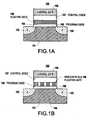
- a conventional flash memory device 100including a substrate 101 , source 102 and drain 103 , formed in the substrate 101 with a channel 104 formed therebetween, a program oxide 105 formed over the substrate 101 , a floating gate 106 formed over the program oxide 105 , a control oxide 107 formed over the floating gate 106 , and a control gate 108 formed over the control oxide 107 .
- a main component of the flash memory device 100 which facilitates this multi-state operationis a conducting floating gate 106 in the gate stack of the transistor (see FIG. 1 (a)) which is coupled to its surroundings (the control gate 108 , and also the channel 104 /source 102 /drain 103 regions) via dielectrics (e.g., 107 , 105 ) on top and below.
- the device 100is programmed by injecting charge into the floating gate 106 (though the program oxide 105 ), and is erased by expelling charge from the floating gate 106 .
- These devices 100are made nonvolatile by decoupling the floating gate 106 from the source 102 /drain 103 /channel 104 and control gate 108 with a sufficiently thick control oxide 107 .
- flash memorycontinues to scale to increasingly higher densities.
- improvements in device speed, power consumption, and endurancee.g., number of times the memory can be read/erased before failing
- flash memory deviceshave improved performance through storage of multiple bits per memory cell (e.g., most notably Intel's StrataFlashTM technology currently stores 2 bits/cell with announced future plans to increase the number of bits/cell). This is achieved by programming the floating gate 106 with different amounts of charge in order to achieve multiple possible threshold voltage (VT) shifts in the same device.
- VTthreshold voltage
- thinning the program oxide 105 thickness in order to achieve lower write/erase voltages (and thus lower power)has the effect of reducing retention times and reliability.
- nanocrystal memory deviceshave been proposed as a way to improve the scaling of flash memory devices, and also as a possible means to achieve robust multi-bit operation (e.g., see H. Hanafi, IEEE Trans. Elect. Dev. 43 1553 (1996); S. Tiwari, F. Rana, H. Hanafi, A. Hartstein, E. Crabbe, C. Chan, Appl. Phys. Lett. 68 1377 (1996); and S. Tiwari, F. Rana, K. Chan, H. Hanafi, W. Chan, D. Buchanan, IEDM 521 (1995)).
- FIG. 1( b )Turning to the conventional nanocrystal memory device 150 shown in FIG. 1( b ), the structure is somewhat similar to that shown in FIG. 1( a ) except that the floating gate 106 is replaced with nanocrystals 156 .
- nanocrystal memory devicesbreaking up a continuous, conducting floating gate 106 into small bits of isolated conducting material can aid in overcoming some of the roadblocks to further scaling.
- the nanocrystal floating gate 156has reduced capacitive coupling to the source 151 /drain region 152 , which leads to a smaller drain turn-on effect.
- the nanocrystal floating gate 106should make the device less susceptible to stress-induced leakage current. That is, if an individual nanocrystal becomes shorted to the channel 154 , other nanocrystals remain unaffected. In a standard floating gate device (e.g., such as device 100 ), any short to the channel 104 is disastrous because charge can no longer be maintained in the floating gate 106 .
- Nanocrystal floating gate devices(e.g., such as those exemplified by reference numeral 150 in FIG. 1( b )) have improved retention characteristics compared to conventional flash devices with the same program oxide thicknesses, because most charge leakage from the floating gate 156 occurs to the heavily doped source 152 /drain regions 153 .
- nanocrystal floating gate devices 150allows scaling to thinner program oxides 155 , which can result in added benefits.
- Thinner oxides 155permit programming at lower voltages using direct quantum mechanical tunneling, rather than Fowler-Nordheim field emission processes.
- nanocrystal memories 150One of the more interesting aspects of nanocrystal memories 150 is the possibility to program the floating gate 156 with discrete numbers of electrons, which in turn leads to multiple discrete, well-defined device threshold voltage (VT) shifts.
- VTdevice threshold voltage
- Table 1 aboveillustrates a calculated charging energy (Ec) and corresponding threshold voltage shift ( ⁇ VT) for nanocrystals of different sizes (e.g., from Tiwari et al., mentioned above).
- Table 1shows that the addition of a single charge to a nanocrystal can result in a significant threshold voltage shift ( ⁇ VT ⁇ 0.5 V for a nanocrystal diameter between 5-10 nm). In this way, it may be possible to use this effect for multi-bit storage, where discrete VT shifts correspond to adding incrementally larger numbers of charges to the floating gate 156 .
- These types of discrete VT shifts from adding single chargeshave been seen experimentally in extremely small devices in which the floating gate 156 contains only a single nanocrystal (e.g., see J. J. Welser, S. Tiwari, S. Rishton, K. Y. Lee, Y. Lee, IEEE Elect. Dev. Lett. 18 278 (1997).
- Kim et al.have also published results on a similar device (e.g., see I. Kim et al., IEEE Electon Dev. Lett. 20 630 (1999)).
- Welser et al.e.g., see above-mentioned J. J. Welser, S. Tiwari, S. Rishton, K. Y. Lee, Y. Lee, IEEE Elect. Dev. Lett. 18 278 (1997), have demonstrated a memory device based on a single nanocrystal in the floating gate. This type of device is often called a “quantum dot memory”. Chou et al. also hold a patent on this device structure (e.g., see U.S. Pat. No. 6,069,380, incorporated herein by reference).
- Ostraat et al.have described operation of a memory device in which the floating gate contains aerosol-deposited silicon nanocrystals (e.g., see M. L. Ostraat et al., Appl. Phys. Lett. 79 433 (2001)).
- nanocrystal floating gate memorieshave been difficult to use for multi-bit memory applications, because of the large nanocrystal size distributions.
- an exemplary feature of the present inventionis to provide a method (and structure) for building a nanocrystal memory device.
- Another exemplary feature of the present inventionis to form a nanocrystal memory device in which a self-assembled material is used to template or define the nanocrystals, and allowing good control over the uniformity of the size of the nanocrystal particles, and over their distribution (e.g., where the nanocrystals are located and the spacing between them).
- a floating gate for a field effect transistorincludes discrete nanoparticles whose dimensions and distribution are defined by a self-assembling material.
- the nanoparticlesmay have diameters between about 2 and about 30 nanometers, with size distributions no greater than substantially 15% of a mean diameter of the nanoparticles.
- a field effect transistorin a second exemplary aspect of the present invention, includes a source region and a drain region formed in a semiconductor material, a channel region disposed between the source region and the drain region, an insulating layer of electrically insulating material disposed over the channel region, a floating gate layer of electrically conducting material disposed over the insulating layer, a layer of electrically insulating material disposed over the floating gate layer, and a gate electrode overlying the layer of insulating material.
- the floating gate layerincludes discrete nanoparticles whose dimensions and distribution are defined by a self-assembling material.
- the nanoparticle densitymay be greater than 10 10 /cm 2 .
- the nanoparticlesmay be arranged in a cubic lattice, or a close-packed, two-dimensional hexagonal lattice.
- the hexagonal latticemay include an average inter-nanoparticle distance between about 1 and about 2 times an average nanoparticle diameter, and a standard deviation of inter-nanoparticle distance no greater than substantially 20% of the mean distance.
- the nanoparticles in the floating gatemay include first and second distinct sizes, each with diameter standard deviations being less than approximately 15% of a mean diameter of the nanoparticles.
- self assemblymay involve a block copolymer film.
- the block copolymermay include a diblock copolymer including a molecular weight within a range of about 5,000 kg/mol to about 250,000 kg/mol.
- a method of forming a floating gate for a field effect transistorincludes forming discrete nanoparticles whose dimensions and distribution are defined using a self-assembled material to template the nanoparticles.
- a method for making a uniform nanoparticle arrayincludes replicating a dimension of a polymer template in a dielectric film, to form a porous dielectric film, conformally depositing a material over the porous dielectric film, and anisotropically and selectively etching the deposited material.
- a method for making a uniform nanoparticle arrayincludes performing a diblock copolymer thin film self assembly over a material film, creating a polymer dot array from the diblock copolymer thin film, and using a polymer dot of the polymer dot array as an etch mask for a nanoparticle reactive ion etching (RIE) of the material film.
- RIEnanoparticle reactive ion etching
- a method for making a uniform nanoparticle arrayincludes performing a diblock copolymer thin film self assembly over silicon, creating a porous polymer film, directionally depositing a first material over the porous polymer film, and dissolving the polymer to lift off at least one region of the first material deposited over the porous polymer.
- a method for making a uniform nanoparticle arrayincludes performing a diblock copolymer thin film self assembly over a first dielectric over an oxidizable material film, creating a porous polymer film, transferring a pattern into the first dielectric, etching the pattern into the material, and thermally oxidizing the material until a narrowest material region between hexagonally-arranged pores close, thereby leaving an array of material nanoparticles.
- a method for making a uniform nanoparticle arrayincludes performing diblock copolymer thin film self assembly over a first dielectric on silicon, creating a porous polymer film, transferring a pattern into the first dielectric, and selectively growing epitaxial silicon off a silicon substrate from within pores to create a silicon nanoparticle array.
- the inventionprovides a method of fabricating a nanocrystal memory device.
- a nanocrystal memory devicecan be formed in which the nanocrystals can be defined using a self-assembly process.
- the nanocrystal memory device(and the method for forming it) allows good control over the uniformity of the size of the nanocrystal particles, and over their distribution (e.g., where the nanocrystals are located and the spacing between them).
- the inventive methodresults in a device having a regular array of such nanocrystals throughout the active area of the device.
- FIG. 1( a )illustrates a schematic diagram of a conventional flash memory device 100 ;
- FIG. 1( b )illustrates a schematic diagram of a conventional nanocrystal memory device 150 ;
- FIG. 2( a )illustrates a top-down scanning electron micrograph (SEM) image of a porous polystyrene (PS) thin film on silicon formed by diblock copolymer self assembly, and in which hexagonally-arranged dark circles are cylindrical holes in the PS film down to the substrate from which the PMMA has been selectively removed;
- SEMscanning electron micrograph
- FIG. 2( b )illustrates a histogram of pore diameters showing a narrow distribution of 10% centered around 20 nm for PS-PMMA molecular weight 67 kg/mol;
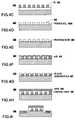
- FIGS. 3 ( a )- 3 ( h )illustrate schematic diagrams depicting silicon nanocrystal array formation based on diblock copolymer self assembly, and more specifically:
- FIG. 3( a )illustrates a step 310 of assembling PS-PMMA diblock copolymer on a thermally-oxidized silicon substrate
- FIG. 3( b )illustrates a step 320 of removing the PMMA block, leaving a porous PS template
- FIG. 3( c )illustrates a step 330 of using reactive ion etching (RIE) to transfer the PS pattern into the oxide film;
- RIEreactive ion etching
- FIG. 3( d )illustrates a step 340 of stripping the remaining polymer, leaving a porous oxide film
- FIG. 3( e )illustrates a step 350 of conformally depositing a material (e.g., silicon);
- FIG. 3( f )illustrates a step 360 of anisotropically etching the silicon
- FIG. 3( g )illustrates a step of 370 stripping oxide to leave the silicon nanocrystal array on silicon
- FIG. 3( h )illustrates a flowchart of the method 300 shown in FIGS. 3 ( a )- 3 ( g );
- FIGS. 4 ( a )- 4 ( j )illustrate a schematic process flow 400 showing formation of a nanocrystal memory device, and more specifically:
- FIG. 4( a )illustrates a step of assembling PS-PMMA diblock copolymer on a thermally-oxidized silicon substrate
- FIG. 4( b )illustrates a step of removing the PMMA block, leaving a porous PS template
- FIG. 4( c )illustrates a step 430 using reactive ion etching (RIE) to transfer the PS pattern into the oxide film;
- RIEreactive ion etching
- FIG. 4( d )illustrates a step of stripping the remaining polymer, leaving a porous oxide film
- FIG. 4( e )illustrates a step of conformally depositing a material (e.g., silicon);
- FIG. 4( f )illustrates a step of anisotropically etching the silicon
- FIG. 4 ( g )illustrates a step of stripping oxide to leave silicon nanocrystal array on silicon
- FIG. 4 ( h )illustrates a step of stripping oxide to leave silicon nanocrystal array on silicon
- FIG. 4 ( i )illustrates a step of stripping oxide to leave silicon nanocrystal array on silicon
- FIG. 4( j )illustrates a flowchart of the method 400 shown in FIGS. 4 ( a )- 4 ( i ).
- FIGS. 2 - 4 ( j )there are shown exemplary embodiments of the method and structures according to the present invention.
- the inventioncan generally take advantage of self-assembling materials which are not exclusively the particular diblock copolymers described below.
- materialswhich naturally form regular arrays, thereby allowing the invention to take advantage of the scale in self-assembling materials.
- nanoparticles which self-assemblethere are proteins which naturally self-assemble, there are block copolymers which naturally self-assemble, there are self-assembled pores in anodized alumina, there are other self-assembling molecules including self-assembled monolayers (SAMs), etc., all of which the invention may be applied advantageously thereto.
- SAMsself-assembled monolayers
- the conventional techniquesmay include using a chemical vapor deposition (CVD) technique to scatter silicon over the sample. While this technique may be somewhat acceptable under some conditions, there is little control of the distribution, and there are small and large sizes randomly over the sample.
- CVDchemical vapor deposition
- Another technique(e.g., on the other extreme from CVD) is using lithography in which patterning occurs, and more specifically a point is written at each location where a particle is to be placed.
- Such a techniqueis very tedious and slow, is not a very manufacturable solution, and does not achieve the resolution or reliability that can be achieved in a self-assembly process.
- the invention's use of self-assemblyovercomes the problems of the conventional techniques and allows controlling the size distribution and positions (e.g., situs) of the particles, as well as a technique which is potentially more manufacturable, simpler, and scalable.
- nanocrystals in the device floating gate according to the present inventionmust be discrete (i.e., electrically isolated from each other), and densely-spaced (e.g., in order to prevent electron conduction by percolation through the silicon channel).
- Nanocrystal sizesshould be highly uniform. Nanocrystal sizes on the order of about 3 nm to about 10 nm diameters should provide sufficient Coulomb charging energies for single-electron charging behavior at room temperature (e.g., see above-mentioned Tiwari et al. article).
- the nanocrystals residing in the gate stackmust be much smaller than this and therefore must be defined using some non-lithographic means.
- the nanocrystalsare preferably patterned using a self-assembly process, which sets (e.g., templates or defines) the dimensions, density, and uniformity of the nanocrystals.
- the characteristic dimensions of self-assembled filmsdepend on fundamental length scales (e.g., such as molecular size), and are therefore inherently more controllable than structures defined using deposition processes, whose size distributions are limited by nucleation and diffusion effects, and sample topography.
- a systemis provided based exemplarily on diblock copolymer self-assembly in one embodiment.
- the inventionis not limited to the diblock copolymer material as mentioned above and would be clearly evident to one of ordinary skill in the art taking the present application as a whole. Indeed, other materials which could be used may include, as mentioned above, self-assembled nanoparticles, anodized alumina, self-assembling proteins, etc.
- diblock copolymer moleculescan microphase separate on a nanometer-scale length scale, thereby forming a hexagonal array of pores in a thin polymer film.
- phase morphologiescould be used for this process and other phase morphologies are achievable (e.g., besides the hexagonal close-packed cylindrical phase morphology described here).
- phase morphologiesmay include spherical phase, the lamellar phase, etc.
- the PS-PMMA diblock copolymersare preferably diluted in a solvent such as toluene or the like, and spin-cast as a thin film preferably having a thickness within a range of about a few nanometers to about a few hundred nanometers onto a sample (e.g., such as a hard mask oxide underneath (e.g., SiO 2 which is thermally grown on silicon) or the like).
- a solventsuch as toluene or the like
- the sampleis heated (e.g., to a temperature within a range of 140° C. to about 200° C., for several hours), thereby to promote the microphase separation (hexagonally close packed (hcp)) array of the exemplary polymers (as shown exemplarily in FIG. 2( a )), which results in an ordered array formation in the film.
- hcphexagonally close packed
- the resulting self assembled film( ⁇ 40 nm thick) is composed of 20-nm-diameter PMMA cylinders (e.g., the black circles shown in FIG. 2( a )) arranged in a hexagonal lattice (40 nm center-to-center spacing) embedded in a matrix of PS (e.g., shown in the white areas in FIG. 2( a ) around the PMMA).
- the temperatureallows this material to phase-separate into the shown ordered pattern.
- the filmPrior to being heated, the film is a mixture of the two polymers which are not physically separated yet.
- “ordered array” for purposes of the present inventionis certainly not limited to hop, and may include others such as spherical or lamellar arrays which result in a different packing arrangement and which depend on the morphology of the materials and the ratio of molecular weights of the two polymers.
- a simple aqueous developing stepe.g., using acetic acid or the like
- acetic acid or the likecan selectively remove the PMMA, leaving a porous PS film (e.g., porous template having a thickness of 40 nm center-to-center spacing of adjacent holes), as shown in FIG. 2( a ).
- the size and density of the holes created in the PSwill be varied depending upon the molecular weights of the materials (e.g., polymers) selected. Thus, choosing a material (e.g., PMMA) with a larger molecular weight will create larger holes (e.g., larger spacings). Greater (or lesser) spacing may be desirable depending upon the application. For example, for a flash memory device, it may be desirable to scale the devices to a smaller physical size, and thereby scaling the size of the nanoparticles at the same time would be desirable. Selectively using the molecular weight of the materials allows such a scaling and control to a smaller size.
- the materialse.g., polymers
- aqueous developing stepinstead of the aqueous developing step, another step could be performed such as etching to leave the topography.
- the inventionis not limited to the aqueous developing step.
- the black circlesindicate where the PMMA resides after it is phase-separated, and the white surrounding the PMMA represents the PS matrix.
- FIG. 2( b )shows a histogram of pore diameters in the PS-PMMA film.
- the narrow distribution (e.g., 10%) around the 20-nm mean-diametershows that these films are highly uniform.
- the characteristic dimensions of features in the self-assembled filmcan be adjusted by beginning with a different copolymer molecular weight, with typical pore diameters ranging from about 10 to about 100 nm.
- FIG. 2( a )shows a top-down SEM image of a porous PS thin film on silicon formed by diblock copolymer self assembly.
- the hexagonally-arranged dark circlesare cylindrical holes in the PS film down to the substrate from which the PMMA has been selectively removed.
- FIG. 2( b )shows a histogram of pore diameters showing a narrow distribution of ⁇ 10% centered around 20 nm for PS-PMMA molecular weight 67 kg/mol.
- the thin porous polymer template formed from diblock copolymer self assemblyis compatible with standard semiconductor processes (e.g., it does not introduce contamination and can be used in a manner similar to a polymer resist for reactive ion etch (RIE) transfer, etc.), and can therefore be used as a mask for transfer of the nanometer-scale pattern into an underlying film or substrate (as described below). (This is often desirable since the polymer template is neither thermally stable nor mechanically robust.)
- FIGS. 3 ( a )- 3 ( g )illustrate schematic diagrams depicting a method 300 (see FIG. 3( h ) showing a flowchart of the process) of silicon nanocrystal array formation based on diblock copolymer self assembly. That is, FIGS. 3 ( a )- 3 ( g ) illustrate schematically how to form a dense array of nanocrystals beginning with a self-assembled PS-PMMA film (e.g., which has been exemplarily formed as described above and shown in FIG. 2( a )).
- a self-assembled PS-PMMA filme.g., which has been exemplarily formed as described above and shown in FIG. 2( a )
- the thin film of PS 303 and PMMA 304is prepared on a thermally oxidized (e.g., SiO 2 or the like 302 ) silicon wafer 301 , as shown in FIG. 3( a ) (step 310 in FIG. 3( h )).
- a thermally oxidized silicon wafer 301e.g., SiO 2 or the like 302
- the PMMA 304is removed from the pores (e.g., as shown in. FIG. 3( b ) and in step 320 ), and the pattern (e.g., PS 303 ) is transferred into the oxide film using a reactive ion etch (RIE) process (e.g., a directional etch using CHF 3 and argon or the like as shown in FIG. 3( c ) and in step 330 ).
- RIEreactive ion etch
- the remaining polymer (PS) 303is removed (e.g., as shown in FIG. 3( d ) and step 340 ), to leave a porous oxide film 302 which has the same dimensions as were in the porous polymer film.
- a thin film 306 of conformally-deposited materiale.g., silicon, such as polysilicon or amorphous silicon, or potentially other materials from which nanocrystals may be formed such as germanium or silicon germanium or metal; an amorphous silicon layer will be assumed in the exemplary process
- the conformally deposited film 306preferably should be continuous and preferably should fully conformally cover the surface.
- the thin film 306has a thickness which is more than about half the pore diameter because the holes must be filled up.
- the thin film 306should be a truly conformal deposition which covers every surface with the same thickness regardless of the surface being a vertical surface or a horizontal surface, in order to fill up or “pinch off” the holes, the thickness deposited should be at least half of the width on either side of the hole in order to pinch together. Thus, the thickness deposited should be at least half of the diameter of the pore.
- a vertical thickness of the deposited silicon layer(e.g., amorphous silicon layer) is much greater inside the hole than it is on top of the oxide.
- the inventiontakes advantage of such a greater thickness to leave material in these holes which will become the silicon nanocrystals.
- the conformally deposited silicon 306is etched using an anisotropic directional etch RIE process that leaves silicon 306 in the pores.
- the directional etch of siliconis performed (e.g., preferably selective against the silicon oxide, but not an etch stop in the conventional sense), stopping on the silicon oxide 302 .
- the inventionensures that the amount of material left in the holes preserves the dimensions of the original polymer film (e.g., no shrinkage or growing thereof).
- the oxide 302is selectively removed using a wet chemical etch or the like such as dilute hydrofluoric acid (HF), thereby resulting in a dense regular array of silicon “dots” (e.g., structures) extending over the sample that reproduce the pore pattern in the original PS-PMMA film.
- a wet chemical etch or the likesuch as dilute hydrofluoric acid (HF)
- the inventioncan form an array of silicon particles having the same dimensions as the polymer pores.
- the oxide 302may be left in building a nanocrystal memory device using the present invention.
- nanocrystal arrayssuch as variations on the etch processes or dielectric films used.
- the dielectric filmsdo not necessarily need to be SiO 2 .
- Such dielectric filmscould be oxide, nitride, high-k, or dielectric film stacks.
- nanocrystals of different materialsuch as germanium, silicon germanium, and metal, can be created by conformal deposition of materials other than silicon, such as germanium, silicon germanium, and/or metal (e.g., different from that of silicon shown in FIG. 3( e )).
- nanoparticlese.g., formed of silicon or the like
- a key advantage of this device structureis that self-assembly is used to define a dense array of uniform nanometer-scale silicon nanocrystals in the gate stack of the FET.
- a key component of the deviceis a gate stack, and hereinbelow is provided a process flow for producing a stack containing uniformly-sized silicon nanocrystals separated from the silicon channel below by a thin program dielectric.
- a substrate 401is provided (e.g., a p-type Si substrate).
- a layer of oxide 402(e.g., exemplarily SiO 2 ) is used, but of course other oxides and nitrides or stack dielectrics or high k dielectrics could be employed is thermally grown on the substrate 401 or deposited by CVD or atomic layer deposition (ALD) or other means, as shown in step 420 and FIG. 4( b ).
- This layer thicknessdefines nanocrystal heights, and may exemplarily be between about 2 to about 20 nm thick.
- the conductivity of the substratecould be different and the invention does not require a p-type substrate.
- step 430 and in FIG. 4( c )the diblock copolymer 403 self assembly process is performed on top of this oxide layer 402 , and the nanometer-scale pattern is transferred into oxide 402 using the RIE process depicted earlier in FIG. 3( c ).
- the polymer 403is stripped, and the wafer cleaned (e.g., by O 02 plasma, and wet chemical cleaner, or the like), thereby leaving a porous dielectric (oxide) film 402 A on silicon 401 , as shown in step 440 and FIG. 4( d ).
- the nanometer-scale holes 404can be optionally shrunk (e.g., to any desired size after the holes are formed) using a nitride deposition and anisotropic etch.
- a fixed polymercould be used, and after the polymer pattern has been transferred into oxide, the holes could be widened or shrunk once they are in the dielectric material.
- the holescould be widened or shrunk once they are in the dielectric material.
- the holescould be further etched (e.g., overetched), which would widen the holes further laterally, but preserve their center positions, center-to-center spacing, and uniformity. This would make the holes larger.
- the holescould be shrunk by depositing a conformal, very thin (e.g., having a thickness of ⁇ 2-8 nm) nitride dielectric deposition, and then performing an anisotropic silicon nitride RIE etch, which leaves a small nitride ring around the edge of the hole, thereby making the hole narrower than before, but preserving the uniformity of the size.
- the size of the nanoparticles(to be built) can be suitably adjusted by this step, and allows setting and precisely controlling the dimensions of the nanoparticles.
- the inventioncan achieve a very precise controlling of the dimensions of every particle, and can set a very precise specification (e.g., a specification can be made for “a particle having a 20 nm ⁇ 1-2 nm, and positioned such that each particles is spaced 40 nm from the next”).
- the inventionhas been shown to achieve a substantially uniform particle spacing (e.g., a center-to-center spacing between adjacent particles) with a variance of no more than 20%. More specifically, the variance of the particle spacing may be no more than about 15%. More specifically, the variance of the particle spacing may be no more than about 10%.
- the inventionhas been shown to achieve a substantially uniform particle spacing, having a variance of the spacing within a range of about 10% to about 20%. This is in contrast to the CVD method in which the particles are typically clustered randomly on the wafer.
- a program oxide 405is thermally grown (e.g., having an exemplary thickness within a range of about 1.5 to about 4 nm).
- step 460a conformal silicon 406 (e.g., similar to the amorphous or polysilicon, etc. as above in step 350 of FIG. 3( e )) is deposited, as shown in FIG. 4( f ).
- a conformal silicon 406e.g., similar to the amorphous or polysilicon, etc. as above in step 350 of FIG. 3( e )
- nanocrystals 407are defined and isolated from each other with an anisotropic silicon RIE which stops when the oxide layer 402 A below is reached.
- the thermal oxide 402 A between the nanocrystalscan be optionally thinned or removed at this stage by selective wet chemical or RIE etching.
- a layer of oxide 408is deposited over (e.g., on top of) the nanocrystals.
- This layer 408will serve as the control oxide in the device (e.g., typical thickness values range from about 4 to about 10 nm).
- the control oxideis formed preferably by deposited low-temperature oxide such as low pressure CVD (LPCVD) oxide (or plasma-enhanced CVD (PECVD) or rapid thermal CVD (RTCVD) or atomic layer deposition (ALD)).
- LPCVDlow pressure CVD
- PECVDplasma-enhanced CVD
- RTCVDrapid thermal CVD
- ALDatomic layer deposition
- the control oxidemay be formed by thermal oxidation (e.g., preferably at a temperature within a range of about 700° to about 1100°) of the silicon nanocrystals.
- the gate material 409is deposited next, and is preferably formed of poly-Si or metal having a suitable thickness.
- the nanocrystalscan optionally be crystallized using a high-temperature anneal. It is noted that typically, the invention may use an amorphous silicon layer which is deposited and then etched. Hence, typically the material is amorphous and not necessarily crystalline. However, the conventional device fabrication methods oftentimes use temperatures which are high enough such that the particles become crystallized. Thus, with the invention, if the temperature was kept relatively low (the temperature range depending, of course, on the material being used), then the amorphous nature of the material could be retained.
- the inventionis not so limited. Indeed, any material could be used so long as the material can be directionally etched and can be conformally deposited. For example, instead of silicon, Ge, SiGe, or another material could be employed for the nanocrystals.
- the devicecan be completed (source/drain patterning, gate contact) using standard FET fabrication processes.
- Such processesmay involve removing the nanocrystals from the source/drain region, patterning the source/drain, and performing a self-aligned source/drain implant to define highly-doped regions. These processes are schematically illustrated in step 490 and in FIG. 4( i ).
- a nanocrystal memory devicecan be formed in which the nanocrystals can be defined using a self-assembly process.
- At least one of a size, spacing, and density of the nanoparticlesmay be templated by the self-assembled material (e.g., as illustrated in FIGS. 4 ( a )- 4 ( j )).
- at least one of the size, spacing, and density of the nanoparticlesmay be defined by the self-assembled material (e.g., where the nanoparticles are separated by the self-assembled material).
- the nanocrystal memory device(and method for forming it) allows good control over the uniformity of the size of the nanocrystal particles, and over their distribution (e.g., where the nanocrystals are located and the spacing between them).
- the inventive methodresults in a device having a regular array of such nanocrystals throughout the active area of the device.
Landscapes
- Engineering & Computer Science (AREA)
- Physics & Mathematics (AREA)
- Chemical & Material Sciences (AREA)
- Nanotechnology (AREA)
- Manufacturing & Machinery (AREA)
- Microelectronics & Electronic Packaging (AREA)
- Power Engineering (AREA)
- Computer Hardware Design (AREA)
- General Physics & Mathematics (AREA)
- Condensed Matter Physics & Semiconductors (AREA)
- Mathematical Physics (AREA)
- Crystallography & Structural Chemistry (AREA)
- Theoretical Computer Science (AREA)
- Inorganic Chemistry (AREA)
- General Chemical & Material Sciences (AREA)
- Chemical Kinetics & Catalysis (AREA)
- Non-Volatile Memory (AREA)
- Semiconductor Memories (AREA)
- Thin Film Transistor (AREA)
Abstract
Description
- 1. Field of the Invention[0001]
- The present invention generally relates to a memory device, and more particularly to a nonvolatile memory device using semiconductor crystals and a method for making the same.[0002]
- 2. Description of the Related Art[0003]
- Nonvolatile memory is ubiquitous in today's technology-laden world, and the most prevalent type of device used to store information is the flash memory.[0004]
- In addition to the need for integrated nonvolatile memory in logic systems, there is a large (and rapidly increasing) market for flash memories as stand-alone storage elements. Cellular telephones and digital cameras are several examples of devices which benefit from nonvolatile flash memory cards.[0005]
- There are various forecasts predicting increased future markets for this type of storage (e.g., see P. Pavan, R. Bez, P. Olivio, and E. Zanoni,[0006]IEEE Proc.85 1248 (1997).
- Flash memory is based on the concept of a field effect transistor (FET) whose threshold voltage (VT) can be reversibly changed between first and second values.[0007]
- As shown in the side sectional view of FIG. 1([0008]a), a conventional
flash memory device 100 is shown including asubstrate 101,source 102 anddrain 103, formed in thesubstrate 101 with achannel 104 formed therebetween, aprogram oxide 105 formed over thesubstrate 101, afloating gate 106 formed over theprogram oxide 105, acontrol oxide 107 formed over thefloating gate 106, and acontrol gate 108 formed over thecontrol oxide 107. - A main component of the[0009]
flash memory device 100 which facilitates this multi-state operation is a conducting floatinggate 106 in the gate stack of the transistor (see FIG. 1 (a)) which is coupled to its surroundings (thecontrol gate 108, and also thechannel 104/source 102/drain 103 regions) via dielectrics (e.g.,107,105) on top and below. - The[0010]
device 100 is programmed by injecting charge into the floating gate106 (though the program oxide105), and is erased by expelling charge from thefloating gate 106. Thesedevices 100 are made nonvolatile by decoupling thefloating gate 106 from thesource 102/drain 103/channel 104 andcontrol gate 108 with a sufficientlythick control oxide 107. - As with all other semiconductor technologies, flash memory continues to scale to increasingly higher densities. At the same time, improvements in device speed, power consumption, and endurance (e.g., number of times the memory can be read/erased before failing) also pay obvious benefits.[0011]
- Finally, some flash memory devices have improved performance through storage of multiple bits per memory cell (e.g., most notably Intel's StrataFlash™ technology currently stores 2 bits/cell with announced future plans to increase the number of bits/cell). This is achieved by programming the[0012]
floating gate 106 with different amounts of charge in order to achieve multiple possible threshold voltage (VT) shifts in the same device. - The pathway to many of these density and performance benefits involves scaling the memory FET, which is becoming increasingly difficult. For example, shrinking the device width in order to improve packing density and speed results in increased drain turn-on effects from capacitive coupling between the[0013]
drain 103 and thefloating gate 106. - Also, thinning the[0014]
program oxide 105 thickness in order to achieve lower write/erase voltages (and thus lower power) has the effect of reducing retention times and reliability. - Referring to FIG. 1([0015]b), nanocrystal memory devices have been proposed as a way to improve the scaling of flash memory devices, and also as a possible means to achieve robust multi-bit operation (e.g., see H. Hanafi,IEEE Trans. Elect. Dev.43 1553 (1996); S. Tiwari, F. Rana, H. Hanafi, A. Hartstein, E. Crabbe, C. Chan,Appl. Phys. Lett.68 1377 (1996); and S. Tiwari, F. Rana, K. Chan, H. Hanafi, W. Chan, D. Buchanan,IEDM521 (1995)).
- Turning to the conventional[0016]
nanocrystal memory device 150 shown in FIG. 1(b), the structure is somewhat similar to that shown in FIG. 1(a) except that thefloating gate 106 is replaced withnanocrystals 156. - That is, a basic idea in nanocrystal memory devices is that breaking up a continuous, conducting floating[0017]
gate 106 into small bits of isolated conducting material can aid in overcoming some of the roadblocks to further scaling. - The nanocrystal floating[0018]
gate 156 has reduced capacitive coupling to thesource 151/drain region 152, which leads to a smaller drain turn-on effect. In addition, the nanocrystal floatinggate 106 should make the device less susceptible to stress-induced leakage current. That is, if an individual nanocrystal becomes shorted to thechannel 154, other nanocrystals remain unaffected. In a standard floating gate device (e.g., such as device100), any short to thechannel 104 is disastrous because charge can no longer be maintained in thefloating gate 106. - Nanocrystal floating gate devices (e.g., such as those exemplified by[0019]
reference numeral 150 in FIG. 1(b)) have improved retention characteristics compared to conventional flash devices with the same program oxide thicknesses, because most charge leakage from thefloating gate 156 occurs to the heavily dopedsource 152/drain regions 153. - In a flash device, such leakage will deplete charge from the entire floating gate, resulting in a loss of memory (e.g., in the same way as stress-induced leakage currents compromise the device).[0020]
- In a nanocrystal device, only those nanocrystals in close proximity to the[0021]
source 152/drain 153 lose their charge by this leakage mechanism, while those farther away (e.g., near the device center) do not. This argument assumes that there is no electrical conduction between nanocrystals in the floating gate156 (e.g., a condition which can be controlled via the nanocrystal density). - The improved retention properties of nanocrystal[0022]
floating gate devices 150 allows scaling tothinner program oxides 155, which can result in added benefits. Thinner oxides155 permit programming at lower voltages using direct quantum mechanical tunneling, rather than Fowler-Nordheim field emission processes. - In addition to the obvious lower-power benefit of lower voltage operation, there is some evidence which suggests that a direct tunneling write/erase mechanism puts less stress on the[0023]
program oxide 155, thereby resulting in increased device cyclability. Modeling also suggests that devices withthinner oxides 155 can be programmed more quickly (e.g., see M. She, Y. C. King, T. J. King, C. Hu,IEEE Device Research Conference,139 (2001)). - One of the more intriguing aspects of[0024]
nanocrystal memories 150 is the possibility to program thefloating gate 156 with discrete numbers of electrons, which in turn leads to multiple discrete, well-defined device threshold voltage (VT) shifts. The idea is that the electrostatic energy necessary to add a single charge to a sufficiently small nanocrystal can become significant. This electrostatic charging energy is given by:
- where e is the electron charge and CΣ is the nanocrystal capacitance to its surroundings. Tiwari et al. have estimated this charging energy for different diameter nanocrystals (in this calculation, the nanocrystals were assumed to be spherical) (e.g., see S. Tiwari, J. A. Wahl, H. Silva, F. Rana, J. J. Welser,[0025]Appl. Phys. A71 403 (2000)). The results are shown in Table 1. The charge stored in the floating gate will shift the device VT by an amount:

- where Q is the amount of charge stored on the[0026]
floating gate 156 and Cctl is the floating gate capacitance to thecontrol gate 158. Tiwari et al. have also computed the AVT for charge stored in different sized nanocrystals. These results are also shown in Table 1 below.TABLE 1 Nanocrystal ΔVT (for a single Diameter (nm) Ec (eV) added charge) (V) 30 .011 .03 20 .018 .06 10 .036 .23 5 .072 .8 2 .178 >5 - Table 1 above illustrates a calculated charging energy (Ec) and corresponding threshold voltage shift (ΔVT) for nanocrystals of different sizes (e.g., from Tiwari et al., mentioned above).[0027]
- Table 1 shows that the addition of a single charge to a nanocrystal can result in a significant threshold voltage shift (ΔVT˜0.5 V for a nanocrystal diameter between 5-10 nm). In this way, it may be possible to use this effect for multi-bit storage, where discrete VT shifts correspond to adding incrementally larger numbers of charges to the[0028]
floating gate 156. These types of discrete VT shifts from adding single charges have been seen experimentally in extremely small devices in which thefloating gate 156 contains only a single nanocrystal (e.g., see J. J. Welser, S. Tiwari, S. Rishton, K. Y. Lee, Y. Lee,IEEE Elect. Dev. Lett.18 278 (1997). - In more conventional devices where the floating[0029]
gate 156 contains many nanocrystals (e.g., instead of a single one), effects due to discrete charging are usually averaged out due to nanocrystal size distributions. - In order to observe this effect (and thus make possible multi-bit storage in the device), it is essential to define all nanocrystals to be of similar size.[0030]
- Several groups have demonstrated implementations of nanocrystal-based flash memories. However, none has defined all nanocrystals to be of similar size by using a self-assembly technique. Tiwari et al. have published numerous papers and also hold a patent (e.g., see U.S. Pat. No. 5,714,766, incorporated herein by reference) on a memory device based on CVD-deposited silicon nanocrystals.[0031]
- Kim et al. have also published results on a similar device (e.g., see I. Kim et al.,[0032]IEEE Electon Dev. Lett.20 630 (1999)). Welser et al. (e.g., see above-mentioned J. J. Welser, S. Tiwari, S. Rishton, K. Y. Lee, Y. Lee,IEEE Elect. Dev. Lett.18 278 (1997), have demonstrated a memory device based on a single nanocrystal in the floating gate. This type of device is often called a “quantum dot memory”. Chou et al. also hold a patent on this device structure (e.g., see U.S. Pat. No. 6,069,380, incorporated herein by reference).
- Ostraat et al. have described operation of a memory device in which the floating gate contains aerosol-deposited silicon nanocrystals (e.g., see M. L. Ostraat et al.,[0033]Appl. Phys. Lett.79 433 (2001)).
- Finally, King et al. have described a device containing germanium nanocrystals (e.g., see . Y. C. King, T. J. King, C. Hu,[0034]IEDM,155 (1998)).
- However, in each of these conventional demonstrations, the nanocrystal sizes were not well-defined, thereby leading to limitations on device performance improvements.[0035]
- Additionally, as mentioned above and prior to the present invention, nanocrystal floating gate memories have been difficult to use for multi-bit memory applications, because of the large nanocrystal size distributions.[0036]
- Further, prior to the present invention, defining all nanocrystals to be of substantially similar size (and thus making possible multi-bit storage in the device), has not been achieved.[0037]
- Moreover, there has been no technique which produces a nanocrystal memory device having nanocrystal size distributions which are substantially uniform, using a self-assembly technique.[0038]
- In sum, the conventional techniques (and subsequently the resulting structure) to make a nanocrystal memory have been notoriously unreliable, and it has been difficult to obtain uniform size of the nanocrystals, and difficult to control the spacing of the distribution around the sample, each of which impact the performance of the device.[0039]
- In view of the foregoing and other problems, drawbacks, and disadvantages of the conventional methods and structures, an exemplary feature of the present invention is to provide a method (and structure) for building a nanocrystal memory device.[0040]
- Another exemplary feature of the present invention is to form a nanocrystal memory device in which a self-assembled material is used to template or define the nanocrystals, and allowing good control over the uniformity of the size of the nanocrystal particles, and over their distribution (e.g., where the nanocrystals are located and the spacing between them).[0041]
- In a first exemplary aspect of the present invention, a floating gate for a field effect transistor, includes discrete nanoparticles whose dimensions and distribution are defined by a self-assembling material. For example, in one explemplary aspect, the nanoparticles may have diameters between about 2 and about 30 nanometers, with size distributions no greater than substantially 15% of a mean diameter of the nanoparticles.[0042]
- In a second exemplary aspect of the present invention, a field effect transistor, includes a source region and a drain region formed in a semiconductor material, a channel region disposed between the source region and the drain region, an insulating layer of electrically insulating material disposed over the channel region, a floating gate layer of electrically conducting material disposed over the insulating layer, a layer of electrically insulating material disposed over the floating gate layer, and a gate electrode overlying the layer of insulating material. The floating gate layer includes discrete nanoparticles whose dimensions and distribution are defined by a self-assembling material.[0043]
- For example, in one exemplary aspect, the nanoparticle density may be greater than 10[0044]10/cm2. In addition, in one exemplary aspect, the nanoparticles may be arranged in a cubic lattice, or a close-packed, two-dimensional hexagonal lattice. Further, the hexagonal lattice may include an average inter-nanoparticle distance between about 1 and about 2 times an average nanoparticle diameter, and a standard deviation of inter-nanoparticle distance no greater than substantially 20% of the mean distance. More specifically, the nanoparticles in the floating gate may include first and second distinct sizes, each with diameter standard deviations being less than approximately 15% of a mean diameter of the nanoparticles.
- Further, in this exemplary aspect of the present invention, self assembly may involve a block copolymer film. For example, the block copolymer may include a diblock copolymer including a molecular weight within a range of about 5,000 kg/mol to about 250,000 kg/mol.[0045]
- In a third exemplary aspect of the present invention, a method of forming a floating gate for a field effect transistor, includes forming discrete nanoparticles whose dimensions and distribution are defined using a self-assembled material to template the nanoparticles.[0046]
- In a fourth exemplary aspect of the present invention, a method for making a uniform nanoparticle array, includes replicating a dimension of a polymer template in a dielectric film, to form a porous dielectric film, conformally depositing a material over the porous dielectric film, and anisotropically and selectively etching the deposited material.[0047]
- In a fifth exemplary aspect of the present invention, a method for making a uniform nanoparticle array, includes performing a diblock copolymer thin film self assembly over a material film, creating a polymer dot array from the diblock copolymer thin film, and using a polymer dot of the polymer dot array as an etch mask for a nanoparticle reactive ion etching (RIE) of the material film.[0048]
- In a sixth exemplary aspect of the present invention, a method for making a uniform nanoparticle array, includes performing a diblock copolymer thin film self assembly over silicon, creating a porous polymer film, directionally depositing a first material over the porous polymer film, and dissolving the polymer to lift off at least one region of the first material deposited over the porous polymer.[0049]
- In a seventh exemplary aspect of the present invention, a method for making a uniform nanoparticle array, includes performing a diblock copolymer thin film self assembly over a first dielectric over an oxidizable material film, creating a porous polymer film, transferring a pattern into the first dielectric, etching the pattern into the material, and thermally oxidizing the material until a narrowest material region between hexagonally-arranged pores close, thereby leaving an array of material nanoparticles.[0050]
- In an eighth exemplary aspect of the present invention, a method for making a uniform nanoparticle array, includes performing diblock copolymer thin film self assembly over a first dielectric on silicon, creating a porous polymer film, transferring a pattern into the first dielectric, and selectively growing epitaxial silicon off a silicon substrate from within pores to create a silicon nanoparticle array.[0051]
- Additionally, the invention provides a method of fabricating a nanocrystal memory device.[0052]
- With the unique and unobvious combination of exemplary features of the invention, a nanocrystal memory device can be formed in which the nanocrystals can be defined using a self-assembly process.[0053]
- Further, the nanocrystal memory device (and the method for forming it) allows good control over the uniformity of the size of the nanocrystal particles, and over their distribution (e.g., where the nanocrystals are located and the spacing between them).[0054]
- Hence, the inventive method results in a device having a regular array of such nanocrystals throughout the active area of the device.[0055]
- The foregoing and other purposes, aspects and advantages will be better understood from the following detailed description of an exemplary embodiment of the invention with reference to the drawings, in which:[0056]
- FIG. 1([0057]a) illustrates a schematic diagram of a conventional
flash memory device 100; - FIG. 1([0058]b) illustrates a schematic diagram of a conventional
nanocrystal memory device 150; - FIG. 2([0059]a) illustrates a top-down scanning electron micrograph (SEM) image of a porous polystyrene (PS) thin film on silicon formed by diblock copolymer self assembly, and in which hexagonally-arranged dark circles are cylindrical holes in the PS film down to the substrate from which the PMMA has been selectively removed;
- FIG. 2([0060]b) illustrates a histogram of pore diameters showing a narrow distribution of 10% centered around 20 nm for PS-PMMA molecular weight 67 kg/mol;
- FIGS.[0061]3(a)-3(h) illustrate schematic diagrams depicting silicon nanocrystal array formation based on diblock copolymer self assembly, and more specifically:
- FIG. 3([0062]a) illustrates a
step 310 of assembling PS-PMMA diblock copolymer on a thermally-oxidized silicon substrate; - FIG. 3([0063]b) illustrates a
step 320 of removing the PMMA block, leaving a porous PS template; - FIG. 3([0064]c) illustrates a
step 330 of using reactive ion etching (RIE) to transfer the PS pattern into the oxide film; - FIG. 3([0065]d) illustrates a
step 340 of stripping the remaining polymer, leaving a porous oxide film; - FIG. 3([0066]e) illustrates a
step 350 of conformally depositing a material (e.g., silicon); - FIG. 3([0067]f) illustrates a
step 360 of anisotropically etching the silicon; and - FIG. 3([0068]g) illustrates a step of370 stripping oxide to leave the silicon nanocrystal array on silicon; and
- FIG. 3([0069]h) illustrates a flowchart of the
method 300 shown in FIGS.3(a)-3(g); and - FIGS.[0070]4(a)-4(j) illustrate a
schematic process flow 400 showing formation of a nanocrystal memory device, and more specifically: - FIG. 4([0071]a) illustrates a step of assembling PS-PMMA diblock copolymer on a thermally-oxidized silicon substrate;
- FIG. 4([0072]b) illustrates a step of removing the PMMA block, leaving a porous PS template;
- FIG. 4([0073]c) illustrates a
step 430 using reactive ion etching (RIE) to transfer the PS pattern into the oxide film; - FIG. 4([0074]d) illustrates a step of stripping the remaining polymer, leaving a porous oxide film;
- FIG. 4([0075]e) illustrates a step of conformally depositing a material (e.g., silicon);
- FIG. 4([0076]f) illustrates a step of anisotropically etching the silicon;
- FIG. 4 ([0077]g) illustrates a step of stripping oxide to leave silicon nanocrystal array on silicon;
- FIG. 4 ([0078]h) illustrates a step of stripping oxide to leave silicon nanocrystal array on silicon;
- FIG. 4 ([0079]i) illustrates a step of stripping oxide to leave silicon nanocrystal array on silicon; and
- FIG. 4([0080]j) illustrates a flowchart of the
method 400 shown in FIGS.4(a)-4(i). - Referring now to the drawings, and more particularly to FIGS.[0081]2-4(j), there are shown exemplary embodiments of the method and structures according to the present invention.
- First, hereinbelow is described an exemplary method for making dense silicon nanocrystal arrays based on self-assembly according to the present invention.[0082]
- It is noted that, while a diblock copolymer is described exemplarily below, the invention is not limited to such materials as would be known by one of ordinary skill in the art, taking the present invention as a whole.[0083]
- That is, the invention can generally take advantage of self-assembling materials which are not exclusively the particular diblock copolymers described below. There are a variety of different material which naturally form regular arrays, thereby allowing the invention to take advantage of the scale in self-assembling materials. Indeed, there are nanoparticles which self-assemble, there are proteins which naturally self-assemble, there are block copolymers which naturally self-assemble, there are self-assembled pores in anodized alumina, there are other self-assembling molecules including self-assembled monolayers (SAMs), etc., all of which the invention may be applied advantageously thereto.[0084]
- The invention's use of self-assembly is clearly different from the conventional techniques. That is, the conventional techniques may include using a chemical vapor deposition (CVD) technique to scatter silicon over the sample. While this technique may be somewhat acceptable under some conditions, there is little control of the distribution, and there are small and large sizes randomly over the sample.[0085]
- Another technique (e.g., on the other extreme from CVD) is using lithography in which patterning occurs, and more specifically a point is written at each location where a particle is to be placed. Such a technique is very tedious and slow, is not a very manufacturable solution, and does not achieve the resolution or reliability that can be achieved in a self-assembly process.[0086]
- Thus, the invention's use of self-assembly overcomes the problems of the conventional techniques and allows controlling the size distribution and positions (e.g., situs) of the particles, as well as a technique which is potentially more manufacturable, simpler, and scalable.[0087]
- In order to achieve the above-mentioned performance improvements over the conventional flash memory and conventional nanocrystal memory devices, the present inventors have discovered that nanocrystals in the device floating gate according to the present invention must be discrete (i.e., electrically isolated from each other), and densely-spaced (e.g., in order to prevent electron conduction by percolation through the silicon channel).[0088]
- For multi-bit memory operation, nanocrystal sizes should be highly uniform. Nanocrystal sizes on the order of about 3 nm to about 10 nm diameters should provide sufficient Coulomb charging energies for single-electron charging behavior at room temperature (e.g., see above-mentioned Tiwari et al. article).[0089]
- Because the transistor device dimensions are typically defined at the limit of lithographic resolution, the nanocrystals residing in the gate stack must be much smaller than this and therefore must be defined using some non-lithographic means.[0090]
- As mentioned above, previous demonstrations have used CVD-deposited or aerosol-deposited nanocrystals, which have inherent size variations.[0091]
- In the present invention, the nanocrystals are preferably patterned using a self-assembly process, which sets (e.g., templates or defines) the dimensions, density, and uniformity of the nanocrystals. The characteristic dimensions of self-assembled films depend on fundamental length scales (e.g., such as molecular size), and are therefore inherently more controllable than structures defined using deposition processes, whose size distributions are limited by nucleation and diffusion effects, and sample topography.[0092]
- There are many self-assembling systems that result in regular arrays of nanometer-scale features.[0093]
- In the present invention, a system is provided based exemplarily on diblock copolymer self-assembly in one embodiment. Obviously, the invention is not limited to the diblock copolymer material as mentioned above and would be clearly evident to one of ordinary skill in the art taking the present application as a whole. Indeed, other materials which could be used may include, as mentioned above, self-assembled nanoparticles, anodized alumina, self-assembling proteins, etc.[0094]
- Under suitable process conditions (e.g., such as molecular weight, block weight ratio, film thickness, annealing conditions, surface treatment and the like), diblock copolymer molecules can microphase separate on a nanometer-scale length scale, thereby forming a hexagonal array of pores in a thin polymer film.[0095]
- Many different polymers (e.g., such as[0096]
- Polybutadiene-polybutylmethcrylate,[0097]
- Polybutadiene-polydimethylsiloxane,[0098]
- polybutadiene-polymethylmethacrylate,[0099]
- polybutadiene-polyvinylpyridine,[0100]
- polyisoprene-polymethylmethacrylate,[0101]
- polyisoprene-polyvinylpyridine,[0102]
- polybutylacrylate-polymethylmethacrylate,[0103]
- polybutylacrylate-polyvinylpyridine,[0104]
- polyhexylacrylate-polyvinylpyridine,[0105]
- polyisobutylene-polybutylmethacrylate,[0106]
- polyisobutylene-polydimethoxysiloxane,[0107]
- polyisobutylene-polymethylmethacrylate,[0108]
- polyisobutylene-polyvinylpyridine,[0109]
- polybutylmethacrylate-polybutylacrylate,[0110]
- polybutylmethacrylate-polyvinylpyridine,[0111]
- polyethylene-polymethylmethacrylate,[0112]
- polymethylmathacrylate-polybutylacrylate,[0113]
- polymethylmethacrylate-polybutylmethacrylate,[0114]
- polystyrene-polybutadiene,[0115]
- polystyrene-polybutylacrylate,[0116]
- polystyrene-polybutylmethacrylate,[0117]
- polystyrene-polybutylstyrene,[0118]
- polystyrene-polydimethoxysiloxane,[0119]
- polystyrene-polyisoprene,[0120]
- polystyrene-polymethylmethacrylate,[0121]
- polystyrene-polyvinylpyridine,[0122]
- polyethylene-polyvinylpyridine,[0123]
- polyvinylpyridine-polymethylmethacrylate,[0124]
- polyethyleneoxide-polyisoprene,[0125]
- polyethyleneoxide-polybutadiene,[0126]
- polyethyleleoxide-polystyrene, and[0127]
- polyetheleneoxide-polymethylmethacrylate[0128]
- could be used for this process and other phase morphologies are achievable (e.g., besides the hexagonal close-packed cylindrical phase morphology described here). For example, other phase morphologies may include spherical phase, the lamellar phase, etc.[0129]
- Hereinbelow and referring first to FIGS.[0130]2(a) and2(b), is detailed an exemplary self-assembly process using diblock copolymers exemplarily including polystyrene (PS) and poly(methyl methacrylate) (PMMA).
- First, the PS-PMMA diblock copolymers are preferably diluted in a solvent such as toluene or the like, and spin-cast as a thin film preferably having a thickness within a range of about a few nanometers to about a few hundred nanometers onto a sample (e.g., such as a hard mask oxide underneath (e.g., SiO[0131]2which is thermally grown on silicon) or the like).
- Then, the sample is heated (e.g., to a temperature within a range of 140° C. to about 200° C., for several hours), thereby to promote the microphase separation (hexagonally close packed (hcp)) array of the exemplary polymers (as shown exemplarily in FIG. 2([0132]a)), which results in an ordered array formation in the film.
- It is noted that it is the temperature which allows the two types of polymers to separate themselves from one another, and gives them mobility. Thus, the temperature and the time are significant, but may vary depending upon the polymer system, with a particular thickness, concentration, etc.[0133]
- For PS-PMMA copolymers having, for example, a molecular weight 67 kg/mol and a mass ratio of 70:30 PS:PMMA, the resulting self assembled film (˜40 nm thick) is composed of 20-nm-diameter PMMA cylinders (e.g., the black circles shown in FIG. 2([0134]a)) arranged in a hexagonal lattice (40 nm center-to-center spacing) embedded in a matrix of PS (e.g., shown in the white areas in FIG. 2(a) around the PMMA). Again, the temperature allows this material to phase-separate into the shown ordered pattern. Prior to being heated, the film is a mixture of the two polymers which are not physically separated yet.
- Again, it is noted that other morphologies can be employed, and thus “ordered array” for purposes of the present invention is certainly not limited to hop, and may include others such as spherical or lamellar arrays which result in a different packing arrangement and which depend on the morphology of the materials and the ratio of molecular weights of the two polymers.[0135]
- Then, a simple aqueous developing step (e.g., using acetic acid or the like) can selectively remove the PMMA, leaving a porous PS film (e.g., porous template having a thickness of 40 nm center-to-center spacing of adjacent holes), as shown in FIG. 2([0136]a).
- The size and density of the holes created in the PS will be varied depending upon the molecular weights of the materials (e.g., polymers) selected. Thus, choosing a material (e.g., PMMA) with a larger molecular weight will create larger holes (e.g., larger spacings). Greater (or lesser) spacing may be desirable depending upon the application. For example, for a flash memory device, it may be desirable to scale the devices to a smaller physical size, and thereby scaling the size of the nanoparticles at the same time would be desirable. Selectively using the molecular weight of the materials allows such a scaling and control to a smaller size.[0137]
- It is noted that, instead of the aqueous developing step, another step could be performed such as etching to leave the topography. Thus, the invention is not limited to the aqueous developing step.[0138]
- Returning to FIG. 2([0139]a), the black circles indicate where the PMMA resides after it is phase-separated, and the white surrounding the PMMA represents the PS matrix.
- FIG. 2([0140]b) shows a histogram of pore diameters in the PS-PMMA film. The narrow distribution (e.g., 10%) around the 20-nm mean-diameter shows that these films are highly uniform.
- The characteristic dimensions of features in the self-assembled film can be adjusted by beginning with a different copolymer molecular weight, with typical pore diameters ranging from about 10 to about 100 nm.[0141]
- Hence, FIG. 2([0142]a) shows a top-down SEM image of a porous PS thin film on silicon formed by diblock copolymer self assembly. The hexagonally-arranged dark circles are cylindrical holes in the PS film down to the substrate from which the PMMA has been selectively removed. FIG. 2(b) shows a histogram of pore diameters showing a narrow distribution of ˜10% centered around 20 nm for PS-PMMA molecular weight 67 kg/mol.
- The thin porous polymer template formed from diblock copolymer self assembly is compatible with standard semiconductor processes (e.g., it does not introduce contamination and can be used in a manner similar to a polymer resist for reactive ion etch (RIE) transfer, etc.), and can therefore be used as a mask for transfer of the nanometer-scale pattern into an underlying film or substrate (as described below). (This is often desirable since the polymer template is neither thermally stable nor mechanically robust.)[0143]
- The above steps will be used in building an exemplary device of interest according to the present invention, and as described below.[0144]
- Exemplary Method of the Present Invention[0145]
- FIGS.[0146]3(a)-3(g) illustrate schematic diagrams depicting a method300 (see FIG. 3(h) showing a flowchart of the process) of silicon nanocrystal array formation based on diblock copolymer self assembly. That is, FIGS.3(a)-3(g) illustrate schematically how to form a dense array of nanocrystals beginning with a self-assembled PS-PMMA film (e.g., which has been exemplarily formed as described above and shown in FIG. 2(a)).
- First, the thin film of[0147]
PS 303 andPMMA 304 is prepared on a thermally oxidized (e.g., SiO2or the like302)silicon wafer 301, as shown in FIG. 3(a) (step 310 in FIG. 3(h)). - Then, the[0148]
PMMA 304 is removed from the pores (e.g., as shown in. FIG. 3(b) and in step320), and the pattern (e.g., PS303) is transferred into the oxide film using a reactive ion etch (RIE) process (e.g., a directional etch using CHF3and argon or the like as shown in FIG. 3(c) and in step330). - Then, the remaining polymer (PS)[0149]303 is removed (e.g., as shown in FIG. 3(d) and step340), to leave a
porous oxide film 302 which has the same dimensions as were in the porous polymer film. - In[0150]
step 350 and as shown in FIG. 3(e), athin film 306 of conformally-deposited material (e.g., silicon, such as polysilicon or amorphous silicon, or potentially other materials from which nanocrystals may be formed such as germanium or silicon germanium or metal; an amorphous silicon layer will be assumed in the exemplary process) is deposited on top of theporous oxide 302. The conformally depositedfilm 306 preferably should be continuous and preferably should fully conformally cover the surface. Preferably, thethin film 306 has a thickness which is more than about half the pore diameter because the holes must be filled up. - That is, since the[0151]
thin film 306 should be a truly conformal deposition which covers every surface with the same thickness regardless of the surface being a vertical surface or a horizontal surface, in order to fill up or “pinch off” the holes, the thickness deposited should be at least half of the width on either side of the hole in order to pinch together. Thus, the thickness deposited should be at least half of the diameter of the pore. - Hence, since a directional etch is to be performed subsequently, it is noted that because of the dimension of the patterns, a vertical thickness of the deposited silicon layer (e.g., amorphous silicon layer) is much greater inside the hole than it is on top of the oxide. The invention takes advantage of such a greater thickness to leave material in these holes which will become the silicon nanocrystals.[0152]
- Then, in[0153]
step 360 and as shown in FIG. 3(f), the conformally depositedsilicon 306 is etched using an anisotropic directional etch RIE process that leavessilicon 306 in the pores. Thus, the directional etch of silicon is performed (e.g., preferably selective against the silicon oxide, but not an etch stop in the conventional sense), stopping on thesilicon oxide 302. However, as mentioned above, it is not a natural stop, and it could be possible to continue to etch and remove all of the silicon in the pores. However, this would not be desirable. - Thus, care must be taken to etch just a sufficient amount of silicon material, such that the silicon remains as discrete particles. Thus, the invention ensures that the amount of material left in the holes preserves the dimensions of the original polymer film (e.g., no shrinkage or growing thereof).[0154]
- As shown in[0155]
step 370 and in FIG. 3(g), optionally, theoxide 302 is selectively removed using a wet chemical etch or the like such as dilute hydrofluoric acid (HF), thereby resulting in a dense regular array of silicon “dots” (e.g., structures) extending over the sample that reproduce the pore pattern in the original PS-PMMA film. - Thus, with the exemplary process above, the invention can form an array of silicon particles having the same dimensions as the polymer pores.[0156]
- It is noted that, as further described below with regard to FIGS.[0157]4(a)-4(g), the
oxide 302 may be left in building a nanocrystal memory device using the present invention. - Several related and similar techniques could be implemented to create nanocrystal arrays, such as variations on the etch processes or dielectric films used. For example, the dielectric films do not necessarily need to be SiO[0158]2. Such dielectric films could be oxide, nitride, high-k, or dielectric film stacks. Also, nanocrystals of different material, such as germanium, silicon germanium, and metal, can be created by conformal deposition of materials other than silicon, such as germanium, silicon germanium, and/or metal (e.g., different from that of silicon shown in FIG. 3(e)).
- Thus, with the exemplary process of the present invention, nanoparticles (e.g., formed of silicon or the like) have been formed having uniform dimensions by self-assembly.[0159]
- Exemplary Process Flow for Nanocrystal Flash Memory Fabrication[0160]
- Hereinbelow, a process flow is described for fabricating the nanocrystal flash memory device, as depicted in FIGS.[0161]4(a)-4(i) and the flowchart of FIG. 4(j), utilizing the nanoparticles having the uniform dimensions as described above.
- A key advantage of this device structure is that self-assembly is used to define a dense array of uniform nanometer-scale silicon nanocrystals in the gate stack of the FET.[0162]
- Gate Stack Formation:[0163]
- A key component of the device is a gate stack, and hereinbelow is provided a process flow for producing a stack containing uniformly-sized silicon nanocrystals separated from the silicon channel below by a thin program dielectric.[0164]
- In[0165]
step 410, asubstrate 401 is provided (e.g., a p-type Si substrate). - Then, a layer of oxide[0166]402 (e.g., exemplarily SiO2) is used, but of course other oxides and nitrides or stack dielectrics or high k dielectrics could be employed is thermally grown on the
substrate 401 or deposited by CVD or atomic layer deposition (ALD) or other means, as shown instep 420 and FIG. 4(b). This layer thickness defines nanocrystal heights, and may exemplarily be between about 2 to about 20 nm thick. As would be evident to one of ordinary skill in the art, the conductivity of the substrate could be different and the invention does not require a p-type substrate. - As shown in[0167]
step 430 and in FIG. 4(c), thediblock copolymer 403 self assembly process is performed on top of thisoxide layer 402, and the nanometer-scale pattern is transferred intooxide 402 using the RIE process depicted earlier in FIG. 3(c). - After the RIE, the[0168]
polymer 403 is stripped, and the wafer cleaned (e.g., by O02plasma, and wet chemical cleaner, or the like), thereby leaving a porous dielectric (oxide) film402A onsilicon 401, as shown instep 440 and FIG. 4(d). - At this stage, the nanometer-[0169]
scale holes 404 can be optionally shrunk (e.g., to any desired size after the holes are formed) using a nitride deposition and anisotropic etch. - That is, as described above, one can start initially with different polymer molecular weights to set (e.g., template or define) any of the size, the distribution and spacing of the holes of the polymer.[0170]
- However, as another option, a fixed polymer could be used, and after the polymer pattern has been transferred into oxide, the holes could be widened or shrunk once they are in the dielectric material. There are two exemplary methods for performing such a widening or shrinking of the holes.[0171]
- First, in FIG. 4([0172]d) in which the PS pattern has been transferred into the oxide to make them porous, the holes could be further etched (e.g., overetched), which would widen the holes further laterally, but preserve their center positions, center-to-center spacing, and uniformity. This would make the holes larger. Alternatively, the holes could be shrunk by depositing a conformal, very thin (e.g., having a thickness of ˜2-8 nm) nitride dielectric deposition, and then performing an anisotropic silicon nitride RIE etch, which leaves a small nitride ring around the edge of the hole, thereby making the hole narrower than before, but preserving the uniformity of the size.
- Thus, the size of the nanoparticles (to be built) can be suitably adjusted by this step, and allows setting and precisely controlling the dimensions of the nanoparticles.[0173]
- Hence, in contrast to the conventional techniques including CVD processes of making a nanocrystal gate device, in which all that can be set is an exemplary particle dimension “which may be within a range of 2-50 nm” and which are scattered randomly all over the wafer with an average distance of “X”, the invention can achieve a very precise controlling of the dimensions of every particle, and can set a very precise specification (e.g., a specification can be made for “a particle having a 20 nm±1-2 nm, and positioned such that each particles is spaced 40 nm from the next”).[0174]
- Hence, a precise spacing and sizing can be obtained by the invention. Indeed, the invention has been shown to achieve a substantially uniform particle spacing (e.g., a center-to-center spacing between adjacent particles) with a variance of no more than 20%. More specifically, the variance of the particle spacing may be no more than about 15%. More specifically, the variance of the particle spacing may be no more than about 10%.[0175]
- Thus, the invention has been shown to achieve a substantially uniform particle spacing, having a variance of the spacing within a range of about 10% to about 20%. This is in contrast to the CVD method in which the particles are typically clustered randomly on the wafer.[0176]
- Next, as shown in[0177]
step 450 and in FIG. 4(e), aprogram oxide 405 is thermally grown (e.g., having an exemplary thickness within a range of about 1.5 to about 4 nm). - This is followed by[0178]
step 460 in which a conformal silicon406 (e.g., similar to the amorphous or polysilicon, etc. as above instep 350 of FIG. 3(e)) is deposited, as shown in FIG. 4(f). - As shown in[0179]
step 470 and in FIG. 4(g),nanocrystals 407 are defined and isolated from each other with an anisotropic silicon RIE which stops when the oxide layer402A below is reached. - The thermal oxide[0180]402A between the nanocrystals can be optionally thinned or removed at this stage by selective wet chemical or RIE etching.
- Next, in[0181]
step 480 and as shown in FIG. 4(h), a layer ofoxide 408 is deposited over (e.g., on top of) the nanocrystals. Thislayer 408 will serve as the control oxide in the device (e.g., typical thickness values range from about 4 to about 10 nm). - The control oxide is formed preferably by deposited low-temperature oxide such as low pressure CVD (LPCVD) oxide (or plasma-enhanced CVD (PECVD) or rapid thermal CVD (RTCVD) or atomic layer deposition (ALD)). Alternatively, the control oxide may be formed by thermal oxidation (e.g., preferably at a temperature within a range of about 700° to about 1100°) of the silicon nanocrystals. The[0182]
gate material 409 is deposited next, and is preferably formed of poly-Si or metal having a suitable thickness. - The nanocrystals can optionally be crystallized using a high-temperature anneal. It is noted that typically, the invention may use an amorphous silicon layer which is deposited and then etched. Hence, typically the material is amorphous and not necessarily crystalline. However, the conventional device fabrication methods oftentimes use temperatures which are high enough such that the particles become crystallized. Thus, with the invention, if the temperature was kept relatively low (the temperature range depending, of course, on the material being used), then the amorphous nature of the material could be retained.[0183]
- It is noted again that, while the exemplary embodiment above, has used silicon to generate the nanocrystals, the invention is not so limited. Indeed, any material could be used so long as the material can be directionally etched and can be conformally deposited. For example, instead of silicon, Ge, SiGe, or another material could be employed for the nanocrystals.[0184]
- Device Patterning:[0185]
- Once the gate stack is grown, the device can be completed (source/drain patterning, gate contact) using standard FET fabrication processes.[0186]
- Such processes may involve removing the nanocrystals from the source/drain region, patterning the source/drain, and performing a self-aligned source/drain implant to define highly-doped regions. These processes are schematically illustrated in[0187]
step 490 and in FIG. 4(i). - Thus, with the unique and unobvious combination of exemplary features of the invention, a nanocrystal memory device can be formed in which the nanocrystals can be defined using a self-assembly process.[0188]
- It is important to note that in the exemplary aspects of the present invention, at least one of a size, spacing, and density of the nanoparticles may be templated by the self-assembled material (e.g., as illustrated in FIGS.[0189]4(a)-4(j)). Alternatively, at least one of the size, spacing, and density of the nanoparticles may be defined by the self-assembled material (e.g., where the nanoparticles are separated by the self-assembled material).
- Further, the nanocrystal memory device (and method for forming it) allows good control over the uniformity of the size of the nanocrystal particles, and over their distribution (e.g., where the nanocrystals are located and the spacing between them). Thus, the inventive method results in a device having a regular array of such nanocrystals throughout the active area of the device.[0190]
- While the invention has been described in terms of several exemplary embodiments, those skilled in the art will recognize that the invention can be practiced with modification within the spirit and scope of the appended claims.[0191]
- Further, it is noted that, Applicant's intent is to encompass equivalents of all claim elements, even if amended later during prosecution.[0192]


Claims (35)
Priority Applications (13)
| Application Number | Priority Date | Filing Date | Title |
|---|---|---|---|
| US10/465,797US7045851B2 (en) | 2003-06-20 | 2003-06-20 | Nonvolatile memory device using semiconductor nanocrystals and method of forming same |
| TW093116874ATWI299575B (en) | 2003-06-20 | 2004-06-11 | Nonvolatile memory device using semiconductor nanocrystals and method of forming same |
| TW095150070ATWI300609B (en) | 2003-06-20 | 2004-06-11 | Nonvolatile memory device using semiconductor nanocrystals and method of forming same |
| PCT/EP2004/051155WO2004114389A1 (en) | 2003-06-20 | 2004-06-17 | Nonvolatile memory device with a floating gate comprising semiconductor nanocrystals |
| EP04741826AEP1647050A1 (en) | 2003-06-20 | 2004-06-17 | Nonvolatile memory device with a floating gate comprising semiconductor nanocrystals |
| KR1020057023246AKR100773012B1 (en) | 2003-06-20 | 2004-06-17 | Nonvolatile memory device with a floating gate comprising semiconductor nanocrystals |
| CN200480015225ACN100587925C (en) | 2003-06-20 | 2004-06-17 | Semiconductor device and method for manufacturing the same |
| IL172520AIL172520A0 (en) | 2003-06-20 | 2005-12-12 | Nonvolatile memory device with a floating gate comprising semiconductor nanocrystals |
| US11/373,127US7985686B2 (en) | 2003-06-20 | 2006-03-13 | Method of forming a nonvolatile memory device using semiconductor nanoparticles |
| US12/545,010US8273665B2 (en) | 2003-06-20 | 2009-08-20 | Nonvolatile memory device using semiconductor nanocrystals and method forming same |
| US13/025,018US8987138B2 (en) | 2003-06-20 | 2011-02-10 | Nonvolatile memory device using semiconductor nanocrystals and method of forming same |
| US13/095,577US8247292B2 (en) | 2003-06-20 | 2011-04-27 | Nonvolative memory device using semiconductor nanocrystals and method of forming same |
| US14/617,647US20150200277A1 (en) | 2003-06-20 | 2015-02-09 | Nonvolatile memory device using semiconductor nanocrystals and method of forming same |
Applications Claiming Priority (1)
| Application Number | Priority Date | Filing Date | Title |
|---|---|---|---|
| US10/465,797US7045851B2 (en) | 2003-06-20 | 2003-06-20 | Nonvolatile memory device using semiconductor nanocrystals and method of forming same |
Related Child Applications (1)
| Application Number | Title | Priority Date | Filing Date |
|---|---|---|---|
| US11/373,127DivisionUS7985686B2 (en) | 2003-06-20 | 2006-03-13 | Method of forming a nonvolatile memory device using semiconductor nanoparticles |
Publications (2)
| Publication Number | Publication Date |
|---|---|
| US20040256662A1true US20040256662A1 (en) | 2004-12-23 |
| US7045851B2 US7045851B2 (en) | 2006-05-16 |
Family
ID=33517590
Family Applications (6)
| Application Number | Title | Priority Date | Filing Date |
|---|---|---|---|
| US10/465,797Expired - LifetimeUS7045851B2 (en) | 2003-06-20 | 2003-06-20 | Nonvolatile memory device using semiconductor nanocrystals and method of forming same |
| US11/373,127Expired - Fee RelatedUS7985686B2 (en) | 2003-06-20 | 2006-03-13 | Method of forming a nonvolatile memory device using semiconductor nanoparticles |
| US12/545,010Expired - Fee RelatedUS8273665B2 (en) | 2003-06-20 | 2009-08-20 | Nonvolatile memory device using semiconductor nanocrystals and method forming same |
| US13/025,018Expired - Fee RelatedUS8987138B2 (en) | 2003-06-20 | 2011-02-10 | Nonvolatile memory device using semiconductor nanocrystals and method of forming same |
| US13/095,577Expired - Fee RelatedUS8247292B2 (en) | 2003-06-20 | 2011-04-27 | Nonvolative memory device using semiconductor nanocrystals and method of forming same |
| US14/617,647AbandonedUS20150200277A1 (en) | 2003-06-20 | 2015-02-09 | Nonvolatile memory device using semiconductor nanocrystals and method of forming same |
Family Applications After (5)
| Application Number | Title | Priority Date | Filing Date |
|---|---|---|---|
| US11/373,127Expired - Fee RelatedUS7985686B2 (en) | 2003-06-20 | 2006-03-13 | Method of forming a nonvolatile memory device using semiconductor nanoparticles |
| US12/545,010Expired - Fee RelatedUS8273665B2 (en) | 2003-06-20 | 2009-08-20 | Nonvolatile memory device using semiconductor nanocrystals and method forming same |
| US13/025,018Expired - Fee RelatedUS8987138B2 (en) | 2003-06-20 | 2011-02-10 | Nonvolatile memory device using semiconductor nanocrystals and method of forming same |
| US13/095,577Expired - Fee RelatedUS8247292B2 (en) | 2003-06-20 | 2011-04-27 | Nonvolative memory device using semiconductor nanocrystals and method of forming same |
| US14/617,647AbandonedUS20150200277A1 (en) | 2003-06-20 | 2015-02-09 | Nonvolatile memory device using semiconductor nanocrystals and method of forming same |
Country Status (7)
| Country | Link |
|---|---|
| US (6) | US7045851B2 (en) |
| EP (1) | EP1647050A1 (en) |
| KR (1) | KR100773012B1 (en) |
| CN (1) | CN100587925C (en) |
| IL (1) | IL172520A0 (en) |
| TW (2) | TWI299575B (en) |
| WO (1) | WO2004114389A1 (en) |
Cited By (67)
| Publication number | Priority date | Publication date | Assignee | Title |
|---|---|---|---|---|
| US20050164132A1 (en)* | 2004-01-28 | 2005-07-28 | Moll Nicolas J. | Nanostructures and methods of making the same |
| US7045851B2 (en)* | 2003-06-20 | 2006-05-16 | International Business Machines Corporation | Nonvolatile memory device using semiconductor nanocrystals and method of forming same |
| US20060193175A1 (en)* | 2005-02-16 | 2006-08-31 | Samsung Electronics Co., Ltd. | Nonvolatile memory device and method of manufacturing the same |
| US20060221672A1 (en)* | 2005-01-11 | 2006-10-05 | The Trustees Of The University Of Pennsylvania | Nanocrystal quantum dot memory devices |
| US20060234418A1 (en)* | 2005-04-19 | 2006-10-19 | Klaus-Dieter Ufert | Method for fabricating a nonvolatile memory element and a nonvolatile memory element |
| US20060237772A1 (en)* | 2005-04-22 | 2006-10-26 | Hynix Semiconductor, Inc. | Method of manufacturing flash memory device |
| US20060261379A1 (en)* | 2005-05-19 | 2006-11-23 | Kabushiki Kaisha Toshiba | Phase change memory and manufacturing method thereof |
| WO2006127589A1 (en)* | 2005-05-23 | 2006-11-30 | Board Of Regents, The University Of Texas System | Nanoparticles in a flash memory using chaperonin proteins |
| US20060273404A1 (en)* | 2005-06-01 | 2006-12-07 | Matrix Semiconductor, Inc. | TFT charge storage memory cell having high-mobility corrugated channel |
| US20060278863A1 (en)* | 2005-06-10 | 2006-12-14 | Chang Heon Y | Phase change ram device and method for fabricating the same |
| US20060281216A1 (en)* | 2005-06-10 | 2006-12-14 | Heon Yong Chang | Method of manufacturing a phase change RAM device utilizing reduced phase change current |
| US20070075353A1 (en)* | 2005-10-05 | 2007-04-05 | Promos Technologies Inc. | Flash memory structure and method for fabricating the same |
| US20070116989A1 (en)* | 2005-11-24 | 2007-05-24 | Hiroshi Ikekame | Magnetic recording media, its fabrication technique, and hard disk drive |
| US20070254488A1 (en)* | 2006-04-28 | 2007-11-01 | Hannu Huotari | Methods for forming roughened surfaces and applications thereof |
| US20080121967A1 (en)* | 2006-09-08 | 2008-05-29 | Ramachandran Muralidhar | Nanocrystal non-volatile memory cell and method therefor |
| US20080217292A1 (en)* | 2007-03-06 | 2008-09-11 | Micron Technology, Inc. | Registered structure formation via the application of directed thermal energy to diblock copolymer films |
| WO2008127293A3 (en)* | 2006-10-19 | 2008-12-11 | Micron Technology Inc | Memory transistor with nanodot floating gate and carbon nanotube control gate and manufacturing method thereof |
| US20080308943A1 (en)* | 2007-06-18 | 2008-12-18 | Elpida Memory, Inc. | Wiring structure and semiconductor device, and their fabrication methods |
| US20080318005A1 (en)* | 2007-06-19 | 2008-12-25 | Millward Dan B | Crosslinkable Graft Polymer Non-Preferentially Wetted by Polystyrene and Polyethylene Oxide |
| US20090062470A1 (en)* | 2007-08-31 | 2009-03-05 | Micron Technology, Inc. | Zwitterionic block copolymers and methods |
| US20090155967A1 (en)* | 2007-12-18 | 2009-06-18 | Vinod Robert Purayath | Method of forming memory with floating gates including self-aligned metal nanodots using a coupling layer |
| US20090166712A1 (en)* | 2006-09-08 | 2009-07-02 | Freescale Semiconductor, Inc. | Nanocrystal non-volatile memory cell and method therefor |
| US7563715B2 (en) | 2005-12-05 | 2009-07-21 | Asm International N.V. | Method of producing thin films |
| EP2088618A1 (en)* | 2008-02-08 | 2009-08-12 | Commissariat a L'Energie Atomique | Method of producing a floating gate |
| US20090200646A1 (en)* | 2008-02-13 | 2009-08-13 | Millward Dan B | One-Dimensional Arrays of Block Copolymer Cylinders and Applications Thereof |
| US20090225602A1 (en)* | 2005-05-26 | 2009-09-10 | Micron Technology, Inc. | Multi-state memory cell |
| US20090240001A1 (en)* | 2008-03-21 | 2009-09-24 | Jennifer Kahl Regner | Methods of Improving Long Range Order in Self-Assembly of Block Copolymer Films with Ionic Liquids |
| US20090236309A1 (en)* | 2008-03-21 | 2009-09-24 | Millward Dan B | Thermal Anneal of Block Copolymer Films with Top Interface Constrained to Wet Both Blocks with Equal Preference |
| US20090263628A1 (en)* | 2008-04-21 | 2009-10-22 | Millward Dan B | Multi-Layer Method for Formation of Registered Arrays of Cylindrical Pores in Polymer Films |
| US20090274887A1 (en)* | 2008-05-02 | 2009-11-05 | Millward Dan B | Graphoepitaxial Self-Assembly of Arrays of Downward Facing Half-Cylinders |
| WO2009099924A3 (en)* | 2008-02-05 | 2009-11-26 | Micron Technology, Inc. | Method to produce nanometer-sized features with directed assembly of block copolymers |
| US20100052018A1 (en)* | 2008-08-26 | 2010-03-04 | International Business Machines Corporation | Continuous metal semiconductor alloy via for interconnects |
| US20100163180A1 (en)* | 2007-03-22 | 2010-07-01 | Millward Dan B | Sub-10 NM Line Features Via Rapid Graphoepitaxial Self-Assembly of Amphiphilic Monolayers |
| CN101863452A (en)* | 2010-06-10 | 2010-10-20 | 中国科学院苏州纳米技术与纳米仿生研究所 | A Method for Improving Fabrication of Nanoarray Structured Devices on Insulating Substrate |
| US20100308412A1 (en)* | 2009-06-03 | 2010-12-09 | International Business Machines Corporation | Control of flatband voltages and threshold voltages in high-k metal gate stacks and structures for cmos devices |
| US20110044115A1 (en)* | 2009-08-21 | 2011-02-24 | Chartered Semiconductor Manufacturing, Ltd. | Non-volatile memory using pyramidal nanocrystals as electron storage elements |
| US20110115026A1 (en)* | 2009-11-16 | 2011-05-19 | International Business Machines Corporation | Control of threshold voltages in high-k metal gate stack and structures for cmos devices |
| WO2012013911A1 (en) | 2010-07-30 | 2012-02-02 | Centre National De La Recherche Scientifique (C.N.R.S) | Thin films organised in nanodomains on the basis of copolymers having polysaccharide blocks for applications in nanotechnology |
| US8193055B1 (en)* | 2007-12-18 | 2012-06-05 | Sandisk Technologies Inc. | Method of forming memory with floating gates including self-aligned metal nanodots using a polymer solution |
| KR101163980B1 (en)* | 2009-08-24 | 2012-07-11 | 한국기초과학지원연구원 | Method of fabricating quantum dot |
| EP2487708A1 (en)* | 2011-02-11 | 2012-08-15 | Commissariat à l'Énergie Atomique et aux Énergies Alternatives | Method for obtaining a network of nanometric terminals |
| US8372295B2 (en) | 2007-04-20 | 2013-02-12 | Micron Technology, Inc. | Extensions of self-assembled structures to increased dimensions via a “bootstrap” self-templating method |
| US8394483B2 (en) | 2007-01-24 | 2013-03-12 | Micron Technology, Inc. | Two-dimensional arrays of holes with sub-lithographic diameters formed by block copolymer self-assembly |
| US8404124B2 (en) | 2007-06-12 | 2013-03-26 | Micron Technology, Inc. | Alternating self-assembling morphologies of diblock copolymers controlled by variations in surfaces |
| US8450418B2 (en) | 2010-08-20 | 2013-05-28 | Micron Technology, Inc. | Methods of forming block copolymers, and block copolymer compositions |
| CN103187245A (en)* | 2011-12-30 | 2013-07-03 | 中芯国际集成电路制造(上海)有限公司 | Method of photoetching of block copolymer through directed self-assembly |
| US8545936B2 (en) | 2008-03-28 | 2013-10-01 | Asm International N.V. | Methods for forming carbon nanotubes |
| US8551808B2 (en) | 2007-06-21 | 2013-10-08 | Micron Technology, Inc. | Methods of patterning a substrate including multilayer antireflection coatings |
| US20140035011A1 (en)* | 2004-06-08 | 2014-02-06 | Sandisk Corporation | Methods and devices for forming nanostructure monolayers and devices including such monolayers |
| US8669645B2 (en) | 2008-10-28 | 2014-03-11 | Micron Technology, Inc. | Semiconductor structures including polymer material permeated with metal oxide |
| US8823075B2 (en) | 2012-11-30 | 2014-09-02 | Sandisk Technologies Inc. | Select gate formation for nanodot flat cell |
| US8822288B2 (en) | 2012-07-02 | 2014-09-02 | Sandisk Technologies Inc. | NAND memory device containing nanodots and method of making thereof |
| US8900963B2 (en) | 2011-11-02 | 2014-12-02 | Micron Technology, Inc. | Methods of forming semiconductor device structures, and related structures |
| US8956713B2 (en) | 2007-04-18 | 2015-02-17 | Micron Technology, Inc. | Methods of forming a stamp and a stamp |
| US8969153B2 (en) | 2013-07-01 | 2015-03-03 | Sandisk Technologies Inc. | NAND string containing self-aligned control gate sidewall cladding |
| US8987802B2 (en)* | 2013-02-28 | 2015-03-24 | Sandisk Technologies Inc. | Method for using nanoparticles to make uniform discrete floating gate layer |
| US9087699B2 (en) | 2012-10-05 | 2015-07-21 | Micron Technology, Inc. | Methods of forming an array of openings in a substrate, and related methods of forming a semiconductor device structure |
| US9139906B2 (en) | 2001-03-06 | 2015-09-22 | Asm America, Inc. | Doping with ALD technology |
| US9177808B2 (en) | 2013-05-21 | 2015-11-03 | Sandisk Technologies Inc. | Memory device with control gate oxygen diffusion control and method of making thereof |
| US9177795B2 (en) | 2013-09-27 | 2015-11-03 | Micron Technology, Inc. | Methods of forming nanostructures including metal oxides |
| EP2839341A4 (en)* | 2012-04-16 | 2015-11-25 | Brewer Science Inc | SILICON HARD MASK LAYER FOR DIRECTED AUTOASSEMBLY |
| US9229328B2 (en) | 2013-05-02 | 2016-01-05 | Micron Technology, Inc. | Methods of forming semiconductor device structures, and related semiconductor device structures |
| US9331181B2 (en) | 2013-03-11 | 2016-05-03 | Sandisk Technologies Inc. | Nanodot enhanced hybrid floating gate for non-volatile memory devices |
| US20190319193A1 (en)* | 2018-04-11 | 2019-10-17 | Soochow University | Auto-polymerization electric storage material based on dopamine, preparation method thereof and application to electric storage device thereof |
| US20190334010A1 (en)* | 2015-09-11 | 2019-10-31 | Intel Corporation | Transistor with dynamic threshold voltage for low-leakage standby and high speed active mode |
| US10483464B1 (en) | 2018-05-31 | 2019-11-19 | Uchicago Argonne, Llc | Resistive switching memory device |
| US12359315B2 (en) | 2019-02-14 | 2025-07-15 | Asm Ip Holding B.V. | Deposition of oxides and nitrides |
Families Citing this family (56)
| Publication number | Priority date | Publication date | Assignee | Title |
|---|---|---|---|---|
| US8568684B2 (en)* | 2000-10-17 | 2013-10-29 | Nanogram Corporation | Methods for synthesizing submicron doped silicon particles |
| US6599631B2 (en) | 2001-01-26 | 2003-07-29 | Nanogram Corporation | Polymer-inorganic particle composites |
| US20090075083A1 (en) | 1997-07-21 | 2009-03-19 | Nanogram Corporation | Nanoparticle production and corresponding structures |
| US7226966B2 (en) | 2001-08-03 | 2007-06-05 | Nanogram Corporation | Structures incorporating polymer-inorganic particle blends |
| WO2005089165A2 (en) | 2004-03-10 | 2005-09-29 | Nanosys, Inc. | Nano-enabled memory devices and anisotropic charge carrying arrays |
| US7595528B2 (en) | 2004-03-10 | 2009-09-29 | Nanosys, Inc. | Nano-enabled memory devices and anisotropic charge carrying arrays |
| US7776758B2 (en) | 2004-06-08 | 2010-08-17 | Nanosys, Inc. | Methods and devices for forming nanostructure monolayers and devices including such monolayers |
| US8563133B2 (en) | 2004-06-08 | 2013-10-22 | Sandisk Corporation | Compositions and methods for modulation of nanostructure energy levels |
| EP1797584A4 (en)* | 2004-06-08 | 2014-08-13 | Sandisk Corp | METHODS AND DEVICES FOR FORMING NANOSTRUCTURE MONOLAYERS AND DEVICES COMPRISING SUCH SINGLES |
| EP1848752A2 (en)* | 2005-01-11 | 2007-10-31 | University Of Massachusetts Lowell | End-capped polymer chains and products thereof |
| TWI240426B (en)* | 2005-01-13 | 2005-09-21 | Chung-Hua Li | Manufacturing method for laminated structure of solar cell, electrode of solar cell, and the solar cell |
| US7309650B1 (en)* | 2005-02-24 | 2007-12-18 | Spansion Llc | Memory device having a nanocrystal charge storage region and method |
| US7391074B2 (en)* | 2005-08-03 | 2008-06-24 | International Business Machines Corporation | Nanowire based non-volatile floating-gate memory |
| US7241695B2 (en)* | 2005-10-06 | 2007-07-10 | Freescale Semiconductor, Inc. | Semiconductor device having nano-pillars and method therefor |
| KR100837413B1 (en)* | 2006-02-28 | 2008-06-12 | 삼성전자주식회사 | Method for producing memory device comprising nanocrystals and the memory device produced hereby |
| TWI395335B (en)* | 2006-06-30 | 2013-05-01 | Applied Materials Inc | Formation of nanocrystals |
| US7667260B2 (en)* | 2006-08-09 | 2010-02-23 | Micron Technology, Inc. | Nanoscale floating gate and methods of formation |
| US7384852B2 (en) | 2006-10-25 | 2008-06-10 | International Business Machines Corporation | Sub-lithographic gate length transistor using self-assembling polymers |
| US7482270B2 (en)* | 2006-12-05 | 2009-01-27 | International Business Machines Corporation | Fully and uniformly silicided gate structure and method for forming same |
| US7847341B2 (en) | 2006-12-20 | 2010-12-07 | Nanosys, Inc. | Electron blocking layers for electronic devices |
| US8686490B2 (en) | 2006-12-20 | 2014-04-01 | Sandisk Corporation | Electron blocking layers for electronic devices |
| US20090136785A1 (en)* | 2007-01-03 | 2009-05-28 | Nanosys, Inc. | Methods for nanopatterning and production of magnetic nanostructures |
| US20080246076A1 (en)* | 2007-01-03 | 2008-10-09 | Nanosys, Inc. | Methods for nanopatterning and production of nanostructures |
| CN101622319B (en) | 2007-01-03 | 2013-05-08 | 内诺格雷姆公司 | Silicon/germanium based nanoparticle inks, doped particles, printing and methods for semiconductor applications |
| US7964107B2 (en)* | 2007-02-08 | 2011-06-21 | Micron Technology, Inc. | Methods using block copolymer self-assembly for sub-lithographic patterning |
| KR100885666B1 (en)* | 2007-05-25 | 2009-02-25 | 한국과학기술원 | Nanostructure comprising organic monolayer and block copolymer and method for producing same |
| US8283258B2 (en)* | 2007-08-16 | 2012-10-09 | Micron Technology, Inc. | Selective wet etching of hafnium aluminum oxide films |
| KR100941021B1 (en)* | 2008-01-21 | 2010-02-05 | 고려대학교 산학협력단 | Method for manufacturing solar cell using triple block copolymer |
| US8215074B2 (en)* | 2008-02-05 | 2012-07-10 | International Business Machines Corporation | Pattern formation employing self-assembled material |
| US8114468B2 (en) | 2008-06-18 | 2012-02-14 | Boise Technology, Inc. | Methods of forming a non-volatile resistive oxide memory array |
| KR101051570B1 (en)* | 2009-01-29 | 2011-07-22 | 주식회사 엘지실트론 | Warp-controlled epitaxial wafer using selective epitaxy and manufacturing method thereof |
| WO2010129884A1 (en)* | 2009-05-08 | 2010-11-11 | 1366 Technologies Inc. | Porous lift-off layer for selective removal of deposited films |
| US8383479B2 (en) | 2009-07-21 | 2013-02-26 | Sandisk Technologies Inc. | Integrated nanostructure-based non-volatile memory fabrication |
| CN102754217B (en)* | 2009-11-17 | 2016-07-06 | 3M创新有限公司 | The textured surfaces of extinction base material |
| TWI408801B (en)* | 2009-12-30 | 2013-09-11 | Univ Nat Taiwan | Non-volatile memory element and method of manufacturing same |
| FR2959349B1 (en) | 2010-04-22 | 2012-09-21 | Commissariat Energie Atomique | MANUFACTURING A MEMORY WITH TWO SELF-ALIGNED INDEPENDENT GRIDS |
| CN101866927A (en)* | 2010-05-12 | 2010-10-20 | 上海宏力半导体制造有限公司 | Word line-sharing contactless nanocrystalline split gate type flash memory |
| US8895962B2 (en) | 2010-06-29 | 2014-11-25 | Nanogram Corporation | Silicon/germanium nanoparticle inks, laser pyrolysis reactors for the synthesis of nanoparticles and associated methods |
| US8535544B2 (en) | 2010-07-26 | 2013-09-17 | International Business Machines Corporation | Structure and method to form nanopore |
| US8138068B2 (en) | 2010-08-11 | 2012-03-20 | International Business Machines Corporation | Method to form nanopore array |
| TWI440218B (en)* | 2010-10-15 | 2014-06-01 | Preparation of nanometer microstructure | |
| CN102456547A (en)* | 2010-10-27 | 2012-05-16 | 和椿科技股份有限公司 | Method for manufacturing nano-micro structure |
| CN103221487A (en) | 2010-11-24 | 2013-07-24 | 道康宁公司 | Controlling morphology of block copolymers |
| CN104919012A (en) | 2013-05-24 | 2015-09-16 | 纳克公司 | Printable ink with silicon/germanium based nanoparticles and with high viscosity alcoholic solvent |
| US9281203B2 (en)* | 2013-08-23 | 2016-03-08 | Taiwan Semiconductor Manufacturing Co., Ltd. | Silicon dot formation by direct self-assembly method for flash memory |
| US9064821B2 (en) | 2013-08-23 | 2015-06-23 | Taiwan Semiconductor Manufacturing Co. Ltd. | Silicon dot formation by self-assembly method and selective silicon growth for flash memory |
| US9228994B1 (en) | 2014-08-06 | 2016-01-05 | Globalfoundries Inc. | Nanochannel electrode devices |
| CN104409460A (en)* | 2014-10-20 | 2015-03-11 | 中国科学院微电子研究所 | Flash memory unit and flash memory device |
| US9812545B2 (en) | 2014-10-30 | 2017-11-07 | City University Of Hong Kong | Electronic device for data storage and a method of producing an electronic device for data storage |
| US9991132B2 (en)* | 2015-04-17 | 2018-06-05 | Taiwan Semiconductor Manufacturing Company, Ltd. | Lithographic technique incorporating varied pattern materials |
| CN105742289A (en)* | 2016-02-26 | 2016-07-06 | 上海华力微电子有限公司 | Flash memory structure |
| CN107170744B (en)* | 2017-04-28 | 2019-10-29 | 中国科学院微电子研究所 | A flash memory cell device and flash memory |
| CN108962899B (en)* | 2017-05-26 | 2021-12-17 | 智瑞佳(苏州)半导体科技有限公司 | Multi-time programmable (MTP) storage unit structure and manufacturing method thereof |
| CN109728076B (en)* | 2018-12-28 | 2020-12-29 | 电子科技大学 | A lateral radiation resistant power device structure |
| CN111863605A (en)* | 2020-07-31 | 2020-10-30 | 合肥维信诺科技有限公司 | Thin film transistor, method of making the same, and display |
| KR20220131561A (en) | 2021-03-12 | 2022-09-29 | 조성진 | Monitoring and control method using a monitoring and control system that supports remote operation based on big data using open source |
Citations (9)
| Publication number | Priority date | Publication date | Assignee | Title |
|---|---|---|---|---|
| US5714766A (en)* | 1995-09-29 | 1998-02-03 | International Business Machines Corporation | Nano-structure memory device |
| US6069380A (en)* | 1997-07-25 | 2000-05-30 | Regents Of The University Of Minnesota | Single-electron floating-gate MOS memory |
| US6090666A (en)* | 1997-09-30 | 2000-07-18 | Sharp Kabushiki Kaisha | Method for fabricating semiconductor nanocrystal and semiconductor memory device using the semiconductor nanocrystal |
| US6310376B1 (en)* | 1997-10-03 | 2001-10-30 | Sharp Kabushiki Kaisha | Semiconductor storage device capable of improving controllability of density and size of floating gate |
| US6320784B1 (en)* | 2000-03-14 | 2001-11-20 | Motorola, Inc. | Memory cell and method for programming thereof |
| US6331463B1 (en)* | 1998-09-19 | 2001-12-18 | United Microelectronics Corp. | Method for manufacturing low power high efficiency non-volatile erasable programmable memory cell structure |
| US6407424B2 (en)* | 1997-01-29 | 2002-06-18 | Micron Technology, Inc. | Flash memory with nanocrystalline silicon film floating gate |
| US6586785B2 (en)* | 2000-06-29 | 2003-07-01 | California Institute Of Technology | Aerosol silicon nanoparticles for use in semiconductor device fabrication |
| US6743406B2 (en)* | 1999-10-22 | 2004-06-01 | The Board Of Trustees Of The University Of Illinois | Family of discretely sized silicon nanoparticles and method for producing the same |
Family Cites Families (30)
| Publication number | Priority date | Publication date | Assignee | Title |
|---|---|---|---|---|
| US4045302A (en) | 1976-07-08 | 1977-08-30 | Burroughs Corporation | Multilevel metallization process |
| US5420067A (en)* | 1990-09-28 | 1995-05-30 | The United States Of America As Represented By The Secretary Of The Navy | Method of fabricatring sub-half-micron trenches and holes |
| KR960005246B1 (en)* | 1992-10-21 | 1996-04-23 | 현대전자산업주식회사 | Method for manufacturing storage electrode of capacitor |
| US5583069A (en)* | 1994-07-08 | 1996-12-10 | Hyundai Electronics Industries Co., Ltd. | Method for making a fine annular charge storage electrode in a semiconductor device using a phase-shift mask |
| US5656205A (en)* | 1994-12-29 | 1997-08-12 | International Business Machines Corporation | Optical components from phase separated block polymers |
| EP0931859B1 (en) | 1996-08-26 | 2008-06-04 | Nippon Telegraph And Telephone Corporation | Method of manufacturing porous anodized alumina film |
| KR100216605B1 (en)* | 1996-12-06 | 1999-08-16 | 정선종 | Method for forming nano-wiring in semiconductor device |
| US5849215A (en) | 1997-01-08 | 1998-12-15 | The Regents Of The University Of California | Highly ordered nanocomposites via a monomer self-assembly in situ condensation approach |
| US5948470A (en) | 1997-04-28 | 1999-09-07 | Harrison; Christopher | Method of nanoscale patterning and products made thereby |
| US6313185B1 (en) | 1998-09-24 | 2001-11-06 | Honeywell International Inc. | Polymers having backbones with reactive groups employed in crosslinking as precursors to nanoporous thin film structures |
| US6705152B2 (en) | 2000-10-24 | 2004-03-16 | Nanoproducts Corporation | Nanostructured ceramic platform for micromachined devices and device arrays |
| US6214746B1 (en) | 1999-05-07 | 2001-04-10 | Honeywell International Inc. | Nanoporous material fabricated using a dissolvable reagent |
| US6536604B1 (en) | 1999-06-25 | 2003-03-25 | C. Jeffrey Brinker | Inorganic dual-layer microporous supported membranes |
| JP4586219B2 (en)* | 1999-09-17 | 2010-11-24 | ソニー株式会社 | Erase method for nonvolatile semiconductor memory device |
| US6171687B1 (en) | 1999-10-18 | 2001-01-09 | Honeywell International Inc. | Infiltrated nanoporous materials and methods of producing same |
| JP2001233674A (en) | 2000-02-24 | 2001-08-28 | Fine Seru:Kk | Method for producing nanoporous carbon material using inorganic template particles |
| WO2001070873A2 (en)* | 2000-03-22 | 2001-09-27 | University Of Massachusetts | Nanocylinder arrays |
| US6271273B1 (en) | 2000-07-14 | 2001-08-07 | Shipley Company, L.L.C. | Porous materials |
| US6589629B1 (en) | 2000-09-11 | 2003-07-08 | Lucent Technologies Inc. | Process for fabricating patterned, functionalized particles and article formed from particles |
| JP3848070B2 (en)* | 2000-09-27 | 2006-11-22 | 株式会社東芝 | Pattern formation method |
| US6358813B1 (en) | 2000-11-15 | 2002-03-19 | International Business Machines Corporation | Method for increasing the capacitance of a semiconductor capacitors |
| CN1305232A (en)* | 2001-02-27 | 2001-07-25 | 南京大学 | MOSFET memory with composite nm-grain Ge/Si float grid structure |
| KR100408520B1 (en) | 2001-05-10 | 2003-12-06 | 삼성전자주식회사 | Single electron memory device comprising quantum dots between gate electrode and single electron storage element and method for manufacturing the same |
| KR100450749B1 (en)* | 2001-12-28 | 2004-10-01 | 한국전자통신연구원 | Method of manufacturing er-doped silicon nano-dot array and laser ablation apparatus used therein |
| US6638441B2 (en)* | 2002-01-07 | 2003-10-28 | Macronix International Co., Ltd. | Method for pitch reduction |
| KR100459895B1 (en)* | 2002-02-09 | 2004-12-04 | 삼성전자주식회사 | Memory device with quantum dot and method of manufacturing the same |
| US7045851B2 (en)* | 2003-06-20 | 2006-05-16 | International Business Machines Corporation | Nonvolatile memory device using semiconductor nanocrystals and method of forming same |
| US7630777B2 (en)* | 2006-07-06 | 2009-12-08 | Honeywell International Inc. | Apparatus and method for configurable process automation in a process control system |
| US7850941B2 (en)* | 2006-10-20 | 2010-12-14 | General Electric Company | Nanostructure arrays and methods for forming same |
| US7544578B2 (en)* | 2007-01-03 | 2009-06-09 | International Business Machines Corporation | Structure and method for stochastic integrated circuit personalization |
- 2003
- 2003-06-20USUS10/465,797patent/US7045851B2/ennot_activeExpired - Lifetime
- 2004
- 2004-06-11TWTW093116874Apatent/TWI299575B/ennot_activeIP Right Cessation
- 2004-06-11TWTW095150070Apatent/TWI300609B/ennot_activeIP Right Cessation
- 2004-06-17EPEP04741826Apatent/EP1647050A1/ennot_activeWithdrawn
- 2004-06-17WOPCT/EP2004/051155patent/WO2004114389A1/enactiveApplication Filing
- 2004-06-17CNCN200480015225Apatent/CN100587925C/ennot_activeExpired - Fee Related
- 2004-06-17KRKR1020057023246Apatent/KR100773012B1/ennot_activeExpired - Fee Related
- 2005
- 2005-12-12ILIL172520Apatent/IL172520A0/enunknown
- 2006
- 2006-03-13USUS11/373,127patent/US7985686B2/ennot_activeExpired - Fee Related
- 2009
- 2009-08-20USUS12/545,010patent/US8273665B2/ennot_activeExpired - Fee Related
- 2011
- 2011-02-10USUS13/025,018patent/US8987138B2/ennot_activeExpired - Fee Related
- 2011-04-27USUS13/095,577patent/US8247292B2/ennot_activeExpired - Fee Related
- 2015
- 2015-02-09USUS14/617,647patent/US20150200277A1/ennot_activeAbandoned
Patent Citations (9)
| Publication number | Priority date | Publication date | Assignee | Title |
|---|---|---|---|---|
| US5714766A (en)* | 1995-09-29 | 1998-02-03 | International Business Machines Corporation | Nano-structure memory device |
| US6407424B2 (en)* | 1997-01-29 | 2002-06-18 | Micron Technology, Inc. | Flash memory with nanocrystalline silicon film floating gate |
| US6069380A (en)* | 1997-07-25 | 2000-05-30 | Regents Of The University Of Minnesota | Single-electron floating-gate MOS memory |
| US6090666A (en)* | 1997-09-30 | 2000-07-18 | Sharp Kabushiki Kaisha | Method for fabricating semiconductor nanocrystal and semiconductor memory device using the semiconductor nanocrystal |
| US6310376B1 (en)* | 1997-10-03 | 2001-10-30 | Sharp Kabushiki Kaisha | Semiconductor storage device capable of improving controllability of density and size of floating gate |
| US6331463B1 (en)* | 1998-09-19 | 2001-12-18 | United Microelectronics Corp. | Method for manufacturing low power high efficiency non-volatile erasable programmable memory cell structure |
| US6743406B2 (en)* | 1999-10-22 | 2004-06-01 | The Board Of Trustees Of The University Of Illinois | Family of discretely sized silicon nanoparticles and method for producing the same |
| US6320784B1 (en)* | 2000-03-14 | 2001-11-20 | Motorola, Inc. | Memory cell and method for programming thereof |
| US6586785B2 (en)* | 2000-06-29 | 2003-07-01 | California Institute Of Technology | Aerosol silicon nanoparticles for use in semiconductor device fabrication |
Cited By (170)
| Publication number | Priority date | Publication date | Assignee | Title |
|---|---|---|---|---|
| US9139906B2 (en) | 2001-03-06 | 2015-09-22 | Asm America, Inc. | Doping with ALD technology |
| US7985686B2 (en) | 2003-06-20 | 2011-07-26 | International Business Machines Corporation | Method of forming a nonvolatile memory device using semiconductor nanoparticles |
| US7045851B2 (en)* | 2003-06-20 | 2006-05-16 | International Business Machines Corporation | Nonvolatile memory device using semiconductor nanocrystals and method of forming same |
| US8273665B2 (en) | 2003-06-20 | 2012-09-25 | International Business Machines Corporation | Nonvolatile memory device using semiconductor nanocrystals and method forming same |
| US8247292B2 (en) | 2003-06-20 | 2012-08-21 | International Business Machines Corporation | Nonvolative memory device using semiconductor nanocrystals and method of forming same |
| US20110201182A1 (en)* | 2003-06-20 | 2011-08-18 | International Business Machines Corporation | Nonvolative memory device using semiconductor nanocrystals and method of forming same |
| US8987138B2 (en) | 2003-06-20 | 2015-03-24 | International Business Machines Corporation | Nonvolatile memory device using semiconductor nanocrystals and method of forming same |
| US20110129973A1 (en)* | 2003-06-20 | 2011-06-02 | International Business Machines Corporation | Nonvolatile memory device using semiconductor nanocrystals and method of forming same |
| US7052618B2 (en)* | 2004-01-28 | 2006-05-30 | Agilent Technologies, Inc. | Nanostructures and methods of making the same |
| US20050164132A1 (en)* | 2004-01-28 | 2005-07-28 | Moll Nicolas J. | Nanostructures and methods of making the same |
| US20140035011A1 (en)* | 2004-06-08 | 2014-02-06 | Sandisk Corporation | Methods and devices for forming nanostructure monolayers and devices including such monolayers |
| US8981452B2 (en)* | 2004-06-08 | 2015-03-17 | Sandisk Corporation | Methods and devices for forming nanostructure monolayers and devices including such monolayers |
| US20060221672A1 (en)* | 2005-01-11 | 2006-10-05 | The Trustees Of The University Of Pennsylvania | Nanocrystal quantum dot memory devices |
| US7813160B2 (en) | 2005-01-11 | 2010-10-12 | The Trustees Of The University Of Pennsylvania | Nanocrystal quantum dot memory devices |
| US7635628B2 (en)* | 2005-02-16 | 2009-12-22 | Samsung Electronics Co., Ltd. | Nonvolatile memory device and method of manufacturing the same |
| US20060193175A1 (en)* | 2005-02-16 | 2006-08-31 | Samsung Electronics Co., Ltd. | Nonvolatile memory device and method of manufacturing the same |
| US20060234418A1 (en)* | 2005-04-19 | 2006-10-19 | Klaus-Dieter Ufert | Method for fabricating a nonvolatile memory element and a nonvolatile memory element |
| US7410868B2 (en)* | 2005-04-19 | 2008-08-12 | Infineon Technologies Ag | Method for fabricating a nonvolatile memory element and a nonvolatile memory element |
| US20060237772A1 (en)* | 2005-04-22 | 2006-10-26 | Hynix Semiconductor, Inc. | Method of manufacturing flash memory device |
| US20080293183A1 (en)* | 2005-05-19 | 2008-11-27 | Kabushiki Kaisha Toshiba | Phase change memory and manufacturing method thereof |
| US20060261379A1 (en)* | 2005-05-19 | 2006-11-23 | Kabushiki Kaisha Toshiba | Phase change memory and manufacturing method thereof |
| US7883930B2 (en) | 2005-05-19 | 2011-02-08 | Kabushiki Kaisha Toshiba | Phase change memory including a plurality of electrically conductive bodies, and manufacturing method thereof |
| US20080191265A1 (en)* | 2005-05-23 | 2008-08-14 | Board Of Regents, The Univeristy Of Texas System | Nanoparticles In a Flash Memory Using Chaperonin Proteins |
| WO2006127589A1 (en)* | 2005-05-23 | 2006-11-30 | Board Of Regents, The University Of Texas System | Nanoparticles in a flash memory using chaperonin proteins |
| US8709892B2 (en)* | 2005-05-23 | 2014-04-29 | Darpa | Nanoparticles in a flash memory using chaperonin proteins |
| US20090225602A1 (en)* | 2005-05-26 | 2009-09-10 | Micron Technology, Inc. | Multi-state memory cell |
| WO2006130801A3 (en)* | 2005-06-01 | 2007-04-12 | Sandisk 3D Llc | Tft charge storage memory cell having high-mobility corrugated channel and method of manufacturing the same |
| US8946017B2 (en) | 2005-06-01 | 2015-02-03 | Sandisk 3D Llc | Method of making a TFT charge storage memory cell having high-mobility corrugated channel |
| US20060273404A1 (en)* | 2005-06-01 | 2006-12-07 | Matrix Semiconductor, Inc. | TFT charge storage memory cell having high-mobility corrugated channel |
| US8110863B2 (en) | 2005-06-01 | 2012-02-07 | Sandisk 3D Llc | TFT charge storage memory cell having high-mobility corrugated channel |
| US20060278863A1 (en)* | 2005-06-10 | 2006-12-14 | Chang Heon Y | Phase change ram device and method for fabricating the same |
| US7332370B2 (en) | 2005-06-10 | 2008-02-19 | Hynix Semiconductor Inc. | Method of manufacturing a phase change RAM device utilizing reduced phase change current |
| KR100842903B1 (en) | 2005-06-10 | 2008-07-02 | 주식회사 하이닉스반도체 | Phase change memory device and manufacturing method thereof |
| US7851776B2 (en) | 2005-06-10 | 2010-12-14 | Hynix Semiconductor Inc. | Phase change RAM device |
| US20110053317A1 (en)* | 2005-06-10 | 2011-03-03 | Hynix Semiconductor Inc. | Phase change ram device and method for fabricating the same |
| US8026125B2 (en) | 2005-06-10 | 2011-09-27 | Hynix Semiconductor Inc. | Phase change RAM device and method for fabricating the same |
| US20060281216A1 (en)* | 2005-06-10 | 2006-12-14 | Heon Yong Chang | Method of manufacturing a phase change RAM device utilizing reduced phase change current |
| KR100668846B1 (en) | 2005-06-10 | 2007-01-16 | 주식회사 하이닉스반도체 | Manufacturing method of phase change memory device |
| JP2006344951A (en)* | 2005-06-10 | 2006-12-21 | Hynix Semiconductor Inc | Phase change memory element and manufacturing method thereof |
| US7223658B2 (en)* | 2005-10-05 | 2007-05-29 | Promos Technologies, Inc. | Flash memory structure and method for fabricating the same |
| US20070075353A1 (en)* | 2005-10-05 | 2007-04-05 | Promos Technologies Inc. | Flash memory structure and method for fabricating the same |
| US20070116989A1 (en)* | 2005-11-24 | 2007-05-24 | Hiroshi Ikekame | Magnetic recording media, its fabrication technique, and hard disk drive |
| US7563715B2 (en) | 2005-12-05 | 2009-07-21 | Asm International N.V. | Method of producing thin films |
| US7491634B2 (en) | 2006-04-28 | 2009-02-17 | Asm International N.V. | Methods for forming roughened surfaces and applications thereof |
| US20090246931A1 (en)* | 2006-04-28 | 2009-10-01 | Asm International N.V. | Methods for Forming Roughened Surfaces and Applications thereof |
| US8252703B2 (en) | 2006-04-28 | 2012-08-28 | Asm International N.V. | Methods for forming roughened surfaces and applications thereof |
| US7923382B2 (en) | 2006-04-28 | 2011-04-12 | Asm International N.V. | Method for forming roughened surface |
| US20070254488A1 (en)* | 2006-04-28 | 2007-11-01 | Hannu Huotari | Methods for forming roughened surfaces and applications thereof |
| US20080121967A1 (en)* | 2006-09-08 | 2008-05-29 | Ramachandran Muralidhar | Nanocrystal non-volatile memory cell and method therefor |
| US7800164B2 (en) | 2006-09-08 | 2010-09-21 | Freescale Semiconductor, Inc. | Nanocrystal non-volatile memory cell and method therefor |
| US20090166712A1 (en)* | 2006-09-08 | 2009-07-02 | Freescale Semiconductor, Inc. | Nanocrystal non-volatile memory cell and method therefor |
| US20100090265A1 (en)* | 2006-10-19 | 2010-04-15 | Micron Technology, Inc. | High density nanodot nonvolatile memory |
| WO2008127293A3 (en)* | 2006-10-19 | 2008-12-11 | Micron Technology Inc | Memory transistor with nanodot floating gate and carbon nanotube control gate and manufacturing method thereof |
| US8394483B2 (en) | 2007-01-24 | 2013-03-12 | Micron Technology, Inc. | Two-dimensional arrays of holes with sub-lithographic diameters formed by block copolymer self-assembly |
| US8512846B2 (en) | 2007-01-24 | 2013-08-20 | Micron Technology, Inc. | Two-dimensional arrays of holes with sub-lithographic diameters formed by block copolymer self-assembly |
| US8409449B2 (en) | 2007-03-06 | 2013-04-02 | Micron Technology, Inc. | Registered structure formation via the application of directed thermal energy to diblock copolymer films |
| US20080217292A1 (en)* | 2007-03-06 | 2008-09-11 | Micron Technology, Inc. | Registered structure formation via the application of directed thermal energy to diblock copolymer films |
| US8753738B2 (en) | 2007-03-06 | 2014-06-17 | Micron Technology, Inc. | Registered structure formation via the application of directed thermal energy to diblock copolymer films |
| US8083953B2 (en) | 2007-03-06 | 2011-12-27 | Micron Technology, Inc. | Registered structure formation via the application of directed thermal energy to diblock copolymer films |
| US8801894B2 (en)* | 2007-03-22 | 2014-08-12 | Micron Technology, Inc. | Sub-10 NM line features via rapid graphoepitaxial self-assembly of amphiphilic monolayers |
| US20100163180A1 (en)* | 2007-03-22 | 2010-07-01 | Millward Dan B | Sub-10 NM Line Features Via Rapid Graphoepitaxial Self-Assembly of Amphiphilic Monolayers |
| US8557128B2 (en) | 2007-03-22 | 2013-10-15 | Micron Technology, Inc. | Sub-10 nm line features via rapid graphoepitaxial self-assembly of amphiphilic monolayers |
| US8784974B2 (en) | 2007-03-22 | 2014-07-22 | Micron Technology, Inc. | Sub-10 NM line features via rapid graphoepitaxial self-assembly of amphiphilic monolayers |
| US8956713B2 (en) | 2007-04-18 | 2015-02-17 | Micron Technology, Inc. | Methods of forming a stamp and a stamp |
| US9768021B2 (en) | 2007-04-18 | 2017-09-19 | Micron Technology, Inc. | Methods of forming semiconductor device structures including metal oxide structures |
| US9276059B2 (en) | 2007-04-18 | 2016-03-01 | Micron Technology, Inc. | Semiconductor device structures including metal oxide structures |
| US8372295B2 (en) | 2007-04-20 | 2013-02-12 | Micron Technology, Inc. | Extensions of self-assembled structures to increased dimensions via a “bootstrap” self-templating method |
| US9142420B2 (en) | 2007-04-20 | 2015-09-22 | Micron Technology, Inc. | Extensions of self-assembled structures to increased dimensions via a “bootstrap” self-templating method |
| US9257256B2 (en) | 2007-06-12 | 2016-02-09 | Micron Technology, Inc. | Templates including self-assembled block copolymer films |
| US8404124B2 (en) | 2007-06-12 | 2013-03-26 | Micron Technology, Inc. | Alternating self-assembling morphologies of diblock copolymers controlled by variations in surfaces |
| US8609221B2 (en) | 2007-06-12 | 2013-12-17 | Micron Technology, Inc. | Alternating self-assembling morphologies of diblock copolymers controlled by variations in surfaces |
| US8080470B2 (en)* | 2007-06-18 | 2011-12-20 | Elpida Memory, Inc. | Wiring structure and semiconductor device, and their fabrication methods |
| US20080308943A1 (en)* | 2007-06-18 | 2008-12-18 | Elpida Memory, Inc. | Wiring structure and semiconductor device, and their fabrication methods |
| US8445592B2 (en) | 2007-06-19 | 2013-05-21 | Micron Technology, Inc. | Crosslinkable graft polymer non-preferentially wetted by polystyrene and polyethylene oxide |
| US8080615B2 (en) | 2007-06-19 | 2011-12-20 | Micron Technology, Inc. | Crosslinkable graft polymer non-preferentially wetted by polystyrene and polyethylene oxide |
| US8513359B2 (en) | 2007-06-19 | 2013-08-20 | Micron Technology, Inc. | Crosslinkable graft polymer non preferentially wetted by polystyrene and polyethylene oxide |
| US8785559B2 (en) | 2007-06-19 | 2014-07-22 | Micron Technology, Inc. | Crosslinkable graft polymer non-preferentially wetted by polystyrene and polyethylene oxide |
| US20080318005A1 (en)* | 2007-06-19 | 2008-12-25 | Millward Dan B | Crosslinkable Graft Polymer Non-Preferentially Wetted by Polystyrene and Polyethylene Oxide |
| US8551808B2 (en) | 2007-06-21 | 2013-10-08 | Micron Technology, Inc. | Methods of patterning a substrate including multilayer antireflection coatings |
| US7732533B2 (en) | 2007-08-31 | 2010-06-08 | Micron Technology, Inc. | Zwitterionic block copolymers and methods |
| US8022147B2 (en) | 2007-08-31 | 2011-09-20 | Micron Technology, Inc. | Zwitterionic block copolymers and methods |
| US20110144275A1 (en)* | 2007-08-31 | 2011-06-16 | Micron Technology, Inc. | Zwitterionic Block Copolymers and Methods |
| US20090062470A1 (en)* | 2007-08-31 | 2009-03-05 | Micron Technology, Inc. | Zwitterionic block copolymers and methods |
| US8236899B2 (en) | 2007-08-31 | 2012-08-07 | Micron Technology, Inc. | Zwitterionic block copolymers and methods |
| WO2009032448A3 (en)* | 2007-08-31 | 2009-08-06 | Micron Technology Inc | Zwitterionic block copolymers and methods |
| US20100204402A1 (en)* | 2007-08-31 | 2010-08-12 | Micron Technology, Inc. | Zwitterionic Block Copolymers And Methods |
| US7910660B2 (en) | 2007-08-31 | 2011-03-22 | Micron Technology, Inc. | Zwitterionic block copolymers and methods |
| US20090155967A1 (en)* | 2007-12-18 | 2009-06-18 | Vinod Robert Purayath | Method of forming memory with floating gates including self-aligned metal nanodots using a coupling layer |
| US7723186B2 (en)* | 2007-12-18 | 2010-05-25 | Sandisk Corporation | Method of forming memory with floating gates including self-aligned metal nanodots using a coupling layer |
| US8263465B2 (en) | 2007-12-18 | 2012-09-11 | Sandisk Technologies Inc. | Method of forming memory with floating gates including self-aligned metal nanodots using a coupling layer |
| US8193055B1 (en)* | 2007-12-18 | 2012-06-05 | Sandisk Technologies Inc. | Method of forming memory with floating gates including self-aligned metal nanodots using a polymer solution |
| US20100190319A1 (en)* | 2007-12-18 | 2010-07-29 | Vinod Robert Purayath | Method of forming memory with floating gates including self-aligned metal nanodots using a coupling layer |
| US10005308B2 (en) | 2008-02-05 | 2018-06-26 | Micron Technology, Inc. | Stamps and methods of forming a pattern on a substrate |
| US11560009B2 (en) | 2008-02-05 | 2023-01-24 | Micron Technology, Inc. | Stamps including a self-assembled block copolymer material, and related methods |
| US8999492B2 (en) | 2008-02-05 | 2015-04-07 | Micron Technology, Inc. | Method to produce nanometer-sized features with directed assembly of block copolymers |
| US10828924B2 (en) | 2008-02-05 | 2020-11-10 | Micron Technology, Inc. | Methods of forming a self-assembled block copolymer material |
| WO2009099924A3 (en)* | 2008-02-05 | 2009-11-26 | Micron Technology, Inc. | Method to produce nanometer-sized features with directed assembly of block copolymers |
| EP2088618A1 (en)* | 2008-02-08 | 2009-08-12 | Commissariat a L'Energie Atomique | Method of producing a floating gate |
| US20090203205A1 (en)* | 2008-02-08 | 2009-08-13 | Commissariat A L'energie Atomique | Method for producing a floating gate with an alternation of lines of first and second materials |
| US7968398B2 (en) | 2008-02-08 | 2011-06-28 | Commissariat A L'energie Atomique | Method for producing a floating gate with an alternation of lines of first and second materials |
| FR2927467A1 (en)* | 2008-02-08 | 2009-08-14 | Commissariat Energie Atomique | METHOD FOR PRODUCING A FLOATING GRID HAVING ALTERNANCE OF LINES IN FIRST AND SECOND MATERIALS |
| US8101261B2 (en) | 2008-02-13 | 2012-01-24 | Micron Technology, Inc. | One-dimensional arrays of block copolymer cylinders and applications thereof |
| US20090200646A1 (en)* | 2008-02-13 | 2009-08-13 | Millward Dan B | One-Dimensional Arrays of Block Copolymer Cylinders and Applications Thereof |
| US8642157B2 (en) | 2008-02-13 | 2014-02-04 | Micron Technology, Inc. | One-dimensional arrays of block copolymer cylinders and applications thereof |
| US11282741B2 (en) | 2008-03-21 | 2022-03-22 | Micron Technology, Inc. | Methods of forming a semiconductor device using block copolymer materials |
| US20090236309A1 (en)* | 2008-03-21 | 2009-09-24 | Millward Dan B | Thermal Anneal of Block Copolymer Films with Top Interface Constrained to Wet Both Blocks with Equal Preference |
| US10153200B2 (en) | 2008-03-21 | 2018-12-11 | Micron Technology, Inc. | Methods of forming a nanostructured polymer material including block copolymer materials |
| US8426313B2 (en) | 2008-03-21 | 2013-04-23 | Micron Technology, Inc. | Thermal anneal of block copolymer films with top interface constrained to wet both blocks with equal preference |
| US20090240001A1 (en)* | 2008-03-21 | 2009-09-24 | Jennifer Kahl Regner | Methods of Improving Long Range Order in Self-Assembly of Block Copolymer Films with Ionic Liquids |
| US9315609B2 (en) | 2008-03-21 | 2016-04-19 | Micron Technology, Inc. | Thermal anneal of block copolymer films with top interface constrained to wet both blocks with equal preference |
| US8633112B2 (en) | 2008-03-21 | 2014-01-21 | Micron Technology, Inc. | Thermal anneal of block copolymer films with top interface constrained to wet both blocks with equal preference |
| US9682857B2 (en) | 2008-03-21 | 2017-06-20 | Micron Technology, Inc. | Methods of improving long range order in self-assembly of block copolymer films with ionic liquids and materials produced therefrom |
| US8641914B2 (en) | 2008-03-21 | 2014-02-04 | Micron Technology, Inc. | Methods of improving long range order in self-assembly of block copolymer films with ionic liquids |
| US8425982B2 (en) | 2008-03-21 | 2013-04-23 | Micron Technology, Inc. | Methods of improving long range order in self-assembly of block copolymer films with ionic liquids |
| US8545936B2 (en) | 2008-03-28 | 2013-10-01 | Asm International N.V. | Methods for forming carbon nanotubes |
| US8114300B2 (en) | 2008-04-21 | 2012-02-14 | Micron Technology, Inc. | Multi-layer method for formation of registered arrays of cylindrical pores in polymer films |
| US8455082B2 (en) | 2008-04-21 | 2013-06-04 | Micron Technology, Inc. | Polymer materials for formation of registered arrays of cylindrical pores |
| US20090263628A1 (en)* | 2008-04-21 | 2009-10-22 | Millward Dan B | Multi-Layer Method for Formation of Registered Arrays of Cylindrical Pores in Polymer Films |
| US8993088B2 (en) | 2008-05-02 | 2015-03-31 | Micron Technology, Inc. | Polymeric materials in self-assembled arrays and semiconductor structures comprising polymeric materials |
| US8114301B2 (en) | 2008-05-02 | 2012-02-14 | Micron Technology, Inc. | Graphoepitaxial self-assembly of arrays of downward facing half-cylinders |
| US20090274887A1 (en)* | 2008-05-02 | 2009-11-05 | Millward Dan B | Graphoepitaxial Self-Assembly of Arrays of Downward Facing Half-Cylinders |
| US8518275B2 (en) | 2008-05-02 | 2013-08-27 | Micron Technology, Inc. | Graphoepitaxial self-assembly of arrays of downward facing half-cylinders |
| US8659093B2 (en) | 2008-08-26 | 2014-02-25 | International Business Machines Corporation | Continuous metal semiconductor alloy via for interconnects |
| US8169031B2 (en) | 2008-08-26 | 2012-05-01 | International Business Machines Corporation | Continuous metal semiconductor alloy via for interconnects |
| US20100052018A1 (en)* | 2008-08-26 | 2010-03-04 | International Business Machines Corporation | Continuous metal semiconductor alloy via for interconnects |
| US8530293B2 (en) | 2008-08-26 | 2013-09-10 | International Businsess Machines Corporation | Continuous metal semiconductor alloy via for interconnects |
| US8669645B2 (en) | 2008-10-28 | 2014-03-11 | Micron Technology, Inc. | Semiconductor structures including polymer material permeated with metal oxide |
| US20100308412A1 (en)* | 2009-06-03 | 2010-12-09 | International Business Machines Corporation | Control of flatband voltages and threshold voltages in high-k metal gate stacks and structures for cmos devices |
| US8748991B2 (en) | 2009-06-03 | 2014-06-10 | International Business Machines Corporation | Control of flatband voltages and threshold voltages in high-k metal gate stacks and structures for CMOS devices |
| US8680629B2 (en)* | 2009-06-03 | 2014-03-25 | International Business Machines Corporation | Control of flatband voltages and threshold voltages in high-k metal gate stacks and structures for CMOS devices |
| US20110044115A1 (en)* | 2009-08-21 | 2011-02-24 | Chartered Semiconductor Manufacturing, Ltd. | Non-volatile memory using pyramidal nanocrystals as electron storage elements |
| US8824208B2 (en) | 2009-08-21 | 2014-09-02 | Globalfoundries Singapore Pte. Ltd. | Non-volatile memory using pyramidal nanocrystals as electron storage elements |
| US8446779B2 (en)* | 2009-08-21 | 2013-05-21 | Globalfoundries Singapore Pte. Ltd. | Non-volatile memory using pyramidal nanocrystals as electron storage elements |
| KR101163980B1 (en)* | 2009-08-24 | 2012-07-11 | 한국기초과학지원연구원 | Method of fabricating quantum dot |
| KR101175325B1 (en)* | 2009-08-24 | 2012-08-20 | 한국기초과학지원연구원 | Method of fabricating quantum dot |
| US8835260B2 (en) | 2009-11-16 | 2014-09-16 | International Business Machines Corporation | Control of threshold voltages in high-k metal gate stack and structures for CMOS devices |
| US20110115026A1 (en)* | 2009-11-16 | 2011-05-19 | International Business Machines Corporation | Control of threshold voltages in high-k metal gate stack and structures for cmos devices |
| US8274116B2 (en) | 2009-11-16 | 2012-09-25 | International Business Machines Corporation | Control of threshold voltages in high-k metal gate stack and structures for CMOS devices |
| CN101863452A (en)* | 2010-06-10 | 2010-10-20 | 中国科学院苏州纳米技术与纳米仿生研究所 | A Method for Improving Fabrication of Nanoarray Structured Devices on Insulating Substrate |
| US9377684B2 (en) | 2010-07-30 | 2016-06-28 | Centre National De La Recherche Scientifique (C.N.R.S) | Thin films organized in nanodomains on the basis of copolymers having polysaccharide blocks for applications in nanotechnology |
| WO2012013911A1 (en) | 2010-07-30 | 2012-02-02 | Centre National De La Recherche Scientifique (C.N.R.S) | Thin films organised in nanodomains on the basis of copolymers having polysaccharide blocks for applications in nanotechnology |
| US8450418B2 (en) | 2010-08-20 | 2013-05-28 | Micron Technology, Inc. | Methods of forming block copolymers, and block copolymer compositions |
| EP2487708A1 (en)* | 2011-02-11 | 2012-08-15 | Commissariat à l'Énergie Atomique et aux Énergies Alternatives | Method for obtaining a network of nanometric terminals |
| FR2971618A1 (en)* | 2011-02-11 | 2012-08-17 | Commissariat Energie Atomique | METHOD FOR OBTAINING A NETWORK OF NANOMETERIC PLOTS |
| US8940623B2 (en) | 2011-02-11 | 2015-01-27 | Commissariat A L'energie Atomique Et Aux Energies Alternatives | Process for obtaining an array of nanodots |
| US9431605B2 (en) | 2011-11-02 | 2016-08-30 | Micron Technology, Inc. | Methods of forming semiconductor device structures |
| US8900963B2 (en) | 2011-11-02 | 2014-12-02 | Micron Technology, Inc. | Methods of forming semiconductor device structures, and related structures |
| CN103187245A (en)* | 2011-12-30 | 2013-07-03 | 中芯国际集成电路制造(上海)有限公司 | Method of photoetching of block copolymer through directed self-assembly |
| EP2839341A4 (en)* | 2012-04-16 | 2015-11-25 | Brewer Science Inc | SILICON HARD MASK LAYER FOR DIRECTED AUTOASSEMBLY |
| US9249013B2 (en) | 2012-04-16 | 2016-02-02 | Brewer Science Inc. | Silicon hardmask layer for directed self-assembly |
| US8822288B2 (en) | 2012-07-02 | 2014-09-02 | Sandisk Technologies Inc. | NAND memory device containing nanodots and method of making thereof |
| US9029936B2 (en) | 2012-07-02 | 2015-05-12 | Sandisk Technologies Inc. | Non-volatile memory structure containing nanodots and continuous metal layer charge traps and method of making thereof |
| US9087699B2 (en) | 2012-10-05 | 2015-07-21 | Micron Technology, Inc. | Methods of forming an array of openings in a substrate, and related methods of forming a semiconductor device structure |
| US8823075B2 (en) | 2012-11-30 | 2014-09-02 | Sandisk Technologies Inc. | Select gate formation for nanodot flat cell |
| US8987802B2 (en)* | 2013-02-28 | 2015-03-24 | Sandisk Technologies Inc. | Method for using nanoparticles to make uniform discrete floating gate layer |
| US9331181B2 (en) | 2013-03-11 | 2016-05-03 | Sandisk Technologies Inc. | Nanodot enhanced hybrid floating gate for non-volatile memory devices |
| US9229328B2 (en) | 2013-05-02 | 2016-01-05 | Micron Technology, Inc. | Methods of forming semiconductor device structures, and related semiconductor device structures |
| US9177808B2 (en) | 2013-05-21 | 2015-11-03 | Sandisk Technologies Inc. | Memory device with control gate oxygen diffusion control and method of making thereof |
| US8969153B2 (en) | 2013-07-01 | 2015-03-03 | Sandisk Technologies Inc. | NAND string containing self-aligned control gate sidewall cladding |
| US9230971B2 (en) | 2013-07-01 | 2016-01-05 | Sandisk Technologies Inc. | NAND string containing self-aligned control gate sidewall cladding |
| US10049874B2 (en) | 2013-09-27 | 2018-08-14 | Micron Technology, Inc. | Self-assembled nanostructures including metal oxides and semiconductor structures comprised thereof |
| US11532477B2 (en) | 2013-09-27 | 2022-12-20 | Micron Technology, Inc. | Self-assembled nanostructures including metal oxides and semiconductor structures comprised thereof |
| US9177795B2 (en) | 2013-09-27 | 2015-11-03 | Micron Technology, Inc. | Methods of forming nanostructures including metal oxides |
| US12400856B2 (en) | 2013-09-27 | 2025-08-26 | Micron Technology, Inc. | Methods of forming nanostructures including metal oxides using block copolymer materials |
| US10720504B2 (en)* | 2015-09-11 | 2020-07-21 | Intel Corporation | Transistor with dynamic threshold voltage for low-leakage standby and high speed active mode |
| US20190334010A1 (en)* | 2015-09-11 | 2019-10-31 | Intel Corporation | Transistor with dynamic threshold voltage for low-leakage standby and high speed active mode |
| US10714690B2 (en)* | 2018-04-11 | 2020-07-14 | Soochow University | Auto-polymerization electric storage material based on dopamine, preparation method thereof and application to electric storage device thereof |
| US20190319193A1 (en)* | 2018-04-11 | 2019-10-17 | Soochow University | Auto-polymerization electric storage material based on dopamine, preparation method thereof and application to electric storage device thereof |
| US10483464B1 (en) | 2018-05-31 | 2019-11-19 | Uchicago Argonne, Llc | Resistive switching memory device |
| US12359315B2 (en) | 2019-02-14 | 2025-07-15 | Asm Ip Holding B.V. | Deposition of oxides and nitrides |
Also Published As
| Publication number | Publication date |
|---|---|
| KR100773012B1 (en) | 2007-11-05 |
| CN100587925C (en) | 2010-02-03 |
| US20090311851A1 (en) | 2009-12-17 |
| IL172520A0 (en) | 2006-04-10 |
| US7045851B2 (en) | 2006-05-16 |
| EP1647050A1 (en) | 2006-04-19 |
| TWI299575B (en) | 2008-08-01 |
| CN1799131A (en) | 2006-07-05 |
| KR20060017532A (en) | 2006-02-23 |
| TW200518349A (en) | 2005-06-01 |
| US8273665B2 (en) | 2012-09-25 |
| US8987138B2 (en) | 2015-03-24 |
| US20110201182A1 (en) | 2011-08-18 |
| US20150200277A1 (en) | 2015-07-16 |
| US20110129973A1 (en) | 2011-06-02 |
| US20060163646A1 (en) | 2006-07-27 |
| US7985686B2 (en) | 2011-07-26 |
| WO2004114389A9 (en) | 2006-02-16 |
| WO2004114389A1 (en) | 2004-12-29 |
| US8247292B2 (en) | 2012-08-21 |
| TWI300609B (en) | 2008-09-01 |
Similar Documents
| Publication | Publication Date | Title |
|---|---|---|
| US7045851B2 (en) | Nonvolatile memory device using semiconductor nanocrystals and method of forming same | |
| US20110018053A1 (en) | Memory cell and methods of manufacturing thereof | |
| US6670670B2 (en) | Single electron memory device comprising quantum dots between gate electrode and single electron storage element and method for manufacturing the same | |
| EP1437775B1 (en) | Method of manufacturing a semiconductor memory device with nano dots | |
| US8263465B2 (en) | Method of forming memory with floating gates including self-aligned metal nanodots using a coupling layer | |
| EP2387066B1 (en) | Method of forming a single-electron memory device using a sub-micron mask | |
| CN1437261A (en) | Memory with quantum point and producing method thereof | |
| CN101267002A (en) | Nonvolatile memory element and manufacturing method thereof | |
| US7391074B2 (en) | Nanowire based non-volatile floating-gate memory | |
| CN101305452A (en) | Programmable structure including nanocrystal memory elements in trenches | |
| US6414333B1 (en) | Single electron transistor using porous silicon | |
| US8193055B1 (en) | Method of forming memory with floating gates including self-aligned metal nanodots using a polymer solution | |
| KR100418182B1 (en) | Method for manufacturing a silicon single electron transistor memory device | |
| KR20050058613A (en) | Memory device and manufacturing method thereof | |
| US9356106B2 (en) | Method to form self-aligned high density nanocrystals | |
| WO2011036214A1 (en) | A memory device and a method of manufacturing the memory device |
Legal Events
| Date | Code | Title | Description |
|---|---|---|---|
| AS | Assignment | Owner name:INTERNATIONAL BUSINESS MACHINES CORPORATION, NEW Y Free format text:ASSIGNMENT OF ASSIGNORS INTEREST;ASSIGNORS:BLACK, CHARLES T.;GUARINI, KATHRYN WILDER;REEL/FRAME:015245/0883 Effective date:20031003 | |
| AS | Assignment | Owner name:INTERNATIONAL BUSINESS MACHINES CORPORATON, NEW YO Free format text:ASSIGNMENT OF ASSIGNORS INTEREST;ASSIGNORS:BLACK, CHARLES T.;GUARINI, KATHRYN WILDER;REEL/FRAME:014864/0048 Effective date:20031003 | |
| FEPP | Fee payment procedure | Free format text:PAYOR NUMBER ASSIGNED (ORIGINAL EVENT CODE: ASPN); ENTITY STATUS OF PATENT OWNER: LARGE ENTITY | |
| STCF | Information on status: patent grant | Free format text:PATENTED CASE | |
| FPAY | Fee payment | Year of fee payment:4 | |
| REMI | Maintenance fee reminder mailed | ||
| FPAY | Fee payment | Year of fee payment:8 | |
| SULP | Surcharge for late payment | Year of fee payment:7 | |
| AS | Assignment | Owner name:GLOBALFOUNDRIES U.S. 2 LLC, NEW YORK Free format text:ASSIGNMENT OF ASSIGNORS INTEREST;ASSIGNOR:INTERNATIONAL BUSINESS MACHINES CORPORATION;REEL/FRAME:036550/0001 Effective date:20150629 | |
| AS | Assignment | Owner name:GLOBALFOUNDRIES INC., CAYMAN ISLANDS Free format text:ASSIGNMENT OF ASSIGNORS INTEREST;ASSIGNORS:GLOBALFOUNDRIES U.S. 2 LLC;GLOBALFOUNDRIES U.S. INC.;REEL/FRAME:036779/0001 Effective date:20150910 | |
| MAFP | Maintenance fee payment | Free format text:PAYMENT OF MAINTENANCE FEE, 12TH YEAR, LARGE ENTITY (ORIGINAL EVENT CODE: M1553) Year of fee payment:12 | |
| AS | Assignment | Owner name:WILMINGTON TRUST, NATIONAL ASSOCIATION, DELAWARE Free format text:SECURITY AGREEMENT;ASSIGNOR:GLOBALFOUNDRIES INC.;REEL/FRAME:049490/0001 Effective date:20181127 | |
| AS | Assignment | Owner name:GLOBALFOUNDRIES U.S. INC., CALIFORNIA Free format text:ASSIGNMENT OF ASSIGNORS INTEREST;ASSIGNOR:GLOBALFOUNDRIES INC.;REEL/FRAME:054633/0001 Effective date:20201022 | |
| AS | Assignment | Owner name:GLOBALFOUNDRIES INC., CAYMAN ISLANDS Free format text:RELEASE BY SECURED PARTY;ASSIGNOR:WILMINGTON TRUST, NATIONAL ASSOCIATION;REEL/FRAME:054636/0001 Effective date:20201117 | |
| AS | Assignment | Owner name:GLOBALFOUNDRIES U.S. INC., NEW YORK Free format text:RELEASE BY SECURED PARTY;ASSIGNOR:WILMINGTON TRUST, NATIONAL ASSOCIATION;REEL/FRAME:056987/0001 Effective date:20201117 |