US20040256657A1 - [flash memory cell structure and method of manufacturing and operating the memory cell] - Google Patents
[flash memory cell structure and method of manufacturing and operating the memory cell]Download PDFInfo
- Publication number
- US20040256657A1 US20040256657A1US10/250,286US25028603AUS2004256657A1US 20040256657 A1US20040256657 A1US 20040256657A1US 25028603 AUS25028603 AUS 25028603AUS 2004256657 A1US2004256657 A1US 2004256657A1
- Authority
- US
- United States
- Prior art keywords
- gate
- dielectric layer
- substrate
- erase
- memory cell
- Prior art date
- Legal status (The legal status is an assumption and is not a legal conclusion. Google has not performed a legal analysis and makes no representation as to the accuracy of the status listed.)
- Abandoned
Links
- 230000015654memoryEffects0.000titleclaimsabstractdescription91
- 238000004519manufacturing processMethods0.000titleclaimsdescription7
- 239000000758substrateSubstances0.000claimsabstractdescription92
- 125000006850spacer groupChemical group0.000claimsabstractdescription38
- 230000005641tunnelingEffects0.000claimsabstractdescription34
- 238000000034methodMethods0.000claimsdescription34
- 230000008569processEffects0.000claimsdescription18
- 229910021420polycrystalline siliconInorganic materials0.000claimsdescription9
- 229920005591polysiliconPolymers0.000claimsdescription9
- 230000003647oxidationEffects0.000claimsdescription8
- 238000007254oxidation reactionMethods0.000claimsdescription8
- 230000000694effectsEffects0.000claimsdescription6
- 239000002784hot electronSubstances0.000claimsdescription6
- 229910052785arsenicInorganic materials0.000claimsdescription2
- 238000000059patterningMethods0.000claims2
- RQNWIZPPADIBDY-UHFFFAOYSA-Narsenic atomChemical compound[As]RQNWIZPPADIBDY-UHFFFAOYSA-N0.000claims1
- 238000011017operating methodMethods0.000claims1
- 230000001960triggered effectEffects0.000claims1
- VYPSYNLAJGMNEJ-UHFFFAOYSA-NSilicium dioxideChemical compoundO=[Si]=OVYPSYNLAJGMNEJ-UHFFFAOYSA-N0.000description10
- 229910052814silicon oxideInorganic materials0.000description10
- 230000015556catabolic processEffects0.000description9
- 239000002131composite materialSubstances0.000description7
- 150000004767nitridesChemical class0.000description6
- 238000005229chemical vapour depositionMethods0.000description5
- 230000005684electric fieldEffects0.000description3
- 238000011065in-situ storageMethods0.000description3
- 238000005468ion implantationMethods0.000description3
- 150000002500ionsChemical class0.000description3
- 230000004888barrier functionEffects0.000description2
- 238000013461designMethods0.000description2
- 239000002019doping agentSubstances0.000description2
- 238000005530etchingMethods0.000description2
- 238000002347injectionMethods0.000description2
- 239000007924injectionSubstances0.000description2
- 238000012986modificationMethods0.000description2
- 230000004048modificationEffects0.000description2
- 230000009467reductionEffects0.000description2
- 230000000717retained effectEffects0.000description2
- -1Arsenic ionsChemical class0.000description1
- MYMOFIZGZYHOMD-UHFFFAOYSA-NDioxygenChemical compoundO=OMYMOFIZGZYHOMD-UHFFFAOYSA-N0.000description1
- 230000005689Fowler Nordheim tunnelingEffects0.000description1
- UFHFLCQGNIYNRP-UHFFFAOYSA-NHydrogenChemical compound[H][H]UFHFLCQGNIYNRP-UHFFFAOYSA-N0.000description1
- 229910052581Si3N4Inorganic materials0.000description1
- 239000004020conductorSubstances0.000description1
- 239000008246gaseous mixtureSubstances0.000description1
- 239000001257hydrogenSubstances0.000description1
- 229910052739hydrogenInorganic materials0.000description1
- 230000005012migrationEffects0.000description1
- 238000013508migrationMethods0.000description1
- 239000001301oxygenSubstances0.000description1
- 229910052760oxygenInorganic materials0.000description1
- 230000035945sensitivityEffects0.000description1
- HQVNEWCFYHHQES-UHFFFAOYSA-Nsilicon nitrideChemical compoundN12[Si]34N5[Si]62N3[Si]51N64HQVNEWCFYHHQES-UHFFFAOYSA-N0.000description1
- 238000012546transferMethods0.000description1
Images


Classifications
- H—ELECTRICITY
- H10—SEMICONDUCTOR DEVICES; ELECTRIC SOLID-STATE DEVICES NOT OTHERWISE PROVIDED FOR
- H10B—ELECTRONIC MEMORY DEVICES
- H10B41/00—Electrically erasable-and-programmable ROM [EEPROM] devices comprising floating gates
- H10B41/30—Electrically erasable-and-programmable ROM [EEPROM] devices comprising floating gates characterised by the memory core region
- H—ELECTRICITY
- H10—SEMICONDUCTOR DEVICES; ELECTRIC SOLID-STATE DEVICES NOT OTHERWISE PROVIDED FOR
- H10B—ELECTRONIC MEMORY DEVICES
- H10B69/00—Erasable-and-programmable ROM [EPROM] devices not provided for in groups H10B41/00 - H10B63/00, e.g. ultraviolet erasable-and-programmable ROM [UVEPROM] devices
- H—ELECTRICITY
- H10—SEMICONDUCTOR DEVICES; ELECTRIC SOLID-STATE DEVICES NOT OTHERWISE PROVIDED FOR
- H10D—INORGANIC ELECTRIC SEMICONDUCTOR DEVICES
- H10D30/00—Field-effect transistors [FET]
- H10D30/60—Insulated-gate field-effect transistors [IGFET]
- H10D30/68—Floating-gate IGFETs
- H10D30/681—Floating-gate IGFETs having only two programming levels
- H10D30/684—Floating-gate IGFETs having only two programming levels programmed by hot carrier injection
- H10D30/685—Floating-gate IGFETs having only two programming levels programmed by hot carrier injection from the channel
- H—ELECTRICITY
- H10—SEMICONDUCTOR DEVICES; ELECTRIC SOLID-STATE DEVICES NOT OTHERWISE PROVIDED FOR
- H10D—INORGANIC ELECTRIC SEMICONDUCTOR DEVICES
- H10D30/00—Field-effect transistors [FET]
- H10D30/60—Insulated-gate field-effect transistors [IGFET]
- H10D30/68—Floating-gate IGFETs
- H10D30/6891—Floating-gate IGFETs characterised by the shapes, relative sizes or dispositions of the floating gate electrode
- H10D30/6892—Floating-gate IGFETs characterised by the shapes, relative sizes or dispositions of the floating gate electrode having at least one additional gate other than the floating gate and the control gate, e.g. program gate, erase gate or select gate
Definitions
- the present inventionrelates to a memory cell device. More particularly, the present invention relates to a flash memory cell structure and a method of manufacturing and operating the memory cell.
- Flash memoryis a memory device that allows multiple data writing, reading and erasing operations. In addition, the stored data will be retained even after power to the device is removed. With these advantages, it has been broadly applied in personal computers and electronic equipment.
- a typical flash memory devicehas a floating gate and a control gate fabricated using doped polysilicon.
- the control gateis set up above the floating gate with an inter-gate dielectric layer separating the two.
- a tunneling oxide layeris also set up between the floating gate and an underlying substrate (the so-called stack gate flash memory).
- a bias voltageis applied to the control gate and the source/drain regions so that an electric field is set up to inject electrons into the floating gate.
- an operating voltageis applied to the control gate. Since the entrapment of charges inside the floating gate will directly affect the opening or closing of the underlying channel, the opening or closing of the channel can be construed as a data value of “1” or “0”.
- the relative potential between the substrate and the drain (source) region or the control gateis raised.
- a tunneling effectcan be utilized to transfer electrons from the floating gate to the substrate or drain (source) via the tunneling oxide layer (the so-called substrate erase or drain [source] side erase) or from the floating gate to the control gate via the inter-gate dielectric layer.
- the select gate(or erase gate) is isolated from the control gate, the floating gate and the substrate through an inter-gate dielectric layer. Hence, if the channel underneath the floating gate conducts even without the application of an operating voltage to the control gate due to serious over-erasure, the channel underneath the select gate (or the erase gate) can still be cut off to prevent any electrical connection between the source/drain regions. In other words, erroneous determination of data value can be prevented.
- FIG. 1is a schematic cross-sectional view of a conventional split-gate flash memory cell.
- the flash memory cellis fabricated on a substrate 100 .
- a tunneling oxide layer 102 , a floating gate 104 , an inter-gate dielectric layer 106 and a control gate 108are sequentially formed over the substrate 100 .
- a spacer 110is formed on the sidewalls and top section of the control gate 106 and another spacer 112 is formed on the sidewall of the floating gate 104 .
- the select gate 114is set up on the sidewall on one side of the floating gate 104 and the control gate 106 .
- a select gate oxide layer 116is set up between the select gate 114 and the substrate 100 .
- a source region 118is set up in the substrate 100 on the side of the floating gate 104 and the control gate 106 where the select gate 114 is absent.
- the drain region 120is set up in the substrate 100 on the side of the floating gate 104 and the control gate 106 where the select gate 114 is present.
- a 10V bias voltageis applied to the control gate 108
- a 10V bias voltageis applied to the select gate 114
- a 6V bias voltageis applied to the source region 118
- 0Vis applied to the drain region 120 .
- the programmingis achieved through the migration of electrons from the drain region 120 to the source region 118 and the injection of electrons from the source region 118 into the floating gate 104 .
- a 0Vis applied to the control gate 108 and a 10V to 12V bias voltage is applied to the select gate 114 while setting the source region 118 and the drain region 120 to a floating state.
- an electric field of considerable intensityis set up between the floating gate 104 and the select gate 114 so that the trapped electrons inside the floating gate 104 are pulled out and transferred to the select gate 114 through the Fowler-Nordheim (F-N) tunneling effect.
- F-NFowler-Nordheim
- the aforementioned flash memory cellutilizes the select gate 114 both as a channel transistor and an erase gate.
- the select gate 114serves as an erase gate during an erasing operation. If the select gate oxide layer has only a moderate thickness, substrate breakdown may occur during the erasing operation. Therefore, the select gate oxide layer 116 must have a thickness capable of preventing a possible substrate breakdown (for example, greater than 200 ⁇ ). However, during a programming operation, the select gate 114 serves as the gate of a channel transistor. If the select gate oxide layer 116 is thick, a greater bias voltage will have to be applied to the select gate 114 just to turn on the channel transistor. In other words, the channel transistor has a high threshold voltage.
- the cell current flowing from the source terminal to the drain terminalwill be reduced leading to a slowdown in the operating speed of the memory cell.
- the channel transistorhas a low threshold voltage
- a greater thickness for the select gate oxide layer 116will lead to a worsening of the channel control by the select gate and an increase in substrate leakage current. Since the memory cell has a high programming sensitivity, programming disturbance may occur with greater frequency.
- one object of the present inventionis to provide a flash memory cell and a method of fabricating and operation the flash memory cell such that current running inside the memory device is increased and programming disturbance within the device is minimized. Hence, overall operating speed of the memory device is improved.
- the flash memory cellincludes a substrate, a tunneling dielectric layer over the substrate, a floating gate over the tunneling dielectric layer, an inter-gate dielectric layer over the floating gate, a control gate over the inter-gate dielectric layer, a first spacer on the sidewall and the top section of the control gate, a second spacer on the sidewall of the floating gate, a source region in the substrate on a first side of the control gate and the floating gate, an erase gate over a source region, an erase gate dielectric layer between the source region and the erase gate, a select gate on a second side of the control gate and the floating gate, a select gate dielectric layer between the substrate and the select gate and a drain region in the substrate on the side close to the select gate.
- the erase gate dielectric layerhas a thickness between about 200 ⁇ to 250 ⁇ 58 .
- the select gate dielectric layerhas a thickness between about 50 ⁇ to 75 ⁇ and the tunneling dielectric layer has a thickness between about 85 ⁇ to 110 ⁇ .
- the erase gateis set up over the source region so that separate erase gate and the select gate are used inside the flash memory cell.
- the thickness of the select gate dielectric layercan be reduced while the thickness of the erase gate dielectric layer can be increased.
- memory cell currentcan be increased when data are read from the memory so that a high operating speed is maintained.
- substrate breakdownis also prevented during a memory erase operation.
- the flash memory cellincludes a substrate, a first gate structure and a second gate structure over the substrate with each gate structure having at least a floating gate over the substrate and a control gate over the floating gate, a source region in the substrate between the first gate structure and the second gate structure, an erase gate above the source region between the first gate structure and the second gate structure, an erase gate dielectric layer between the source region and the erase gate, a first select gate and a second select gate on the sidewall of the first gate structure and the second gate structure away from the source region, a select gate dielectric layer between the substrate and the first and the second select gate and a drain region in the substrate just outside the first select gate and the second select gate.
- the erase gate dielectric layerhas a thickness between about 200 ⁇ to 250 ⁇ .
- the select gate dielectric layerhas a thickness between about 50 ⁇ to 75 ⁇ and the tunneling dielectric layer has a thickness between about 85 ⁇ to 110 ⁇ .
- the erase gateis set up over the source region between the first gate structure and the second gate structure so that separate erase gate and the select gate are used inside the flash memory cell.
- the thickness of the select gate dielectric layercan be reduced while the thickness of the erase gate dielectric layer can be increased.
- memory cell currentcan be increased when data are read from the memory so that a high operating speed is maintained.
- substrate breakdownis also prevented during a memory erase operation.
- This inventionalso provides a method of fabricating a flash memory cell.
- a substrate having a first gate structure and a second gate structure thereonis provided.
- the first gate structure and the second gate structureeach includes a tunneling dielectric layer formed over the substrate, a floating gate formed over the tunneling dielectric layer, an inter-gate dielectric layer formed over the floating gate, a control gate formed over the inter-gate dielectric layer and a first spacer formed on the sidewall and top section of the control gate.
- a source regionis formed in the substrate between the first gate structure and the second gate structure.
- An erase gate dielectric layeris formed over the surface of the source region.
- a second spaceris formed on the sidewall of the floating gate.
- An erase gateis formed over the source region such that the erase gate fills up the space between the first gate structure and the second gate structure.
- a select gate dielectric layeris formed over the substrate.
- a first select gate and a second select gateare formed on the sidewall of the third spacers.
- a first drain region and a second drain regionare formed in the substrate on one side of the first select gate and the second select gate.
- the first gate structure and the second gate structureare formed before forming a first dielectric layer, a first conductive layer and a second dielectric layer sequentially over the substrate. Thereafter, a second conductive layer is formed over the second dielectric layer and then the second conductive layer is patterned to form the control gate. Next, a first spacer is formed on the sidewalls and the top section of the control gate. Using the first spacer and the control gate as a mask, the second dielectric layer, the first conductive layer, the first dielectric layer are patterned to form an inter-gate dielectric layer, a floating gate and a tunneling dielectric layer.
- a conductive layeris formed over a source region to fabricate the erase gate so that the erase gate and the select gate are separate devices.
- the erase gate dielectric layercan have a greater thickness (for example, greater than 200 ⁇ ) while the select gate dielectric layer underneath the select gate can be thinner (for example, about 65 ⁇ ).
- the threshold voltage for triggering the memory deviceis reduced and cell current flowing inside the memory device is increased.
- programming disturbanceis minimized so that the memory cell can operate faster.
- substrate breakdown during an erasing operationis prevented.
- This inventionalso provides a method of operating a flash memory cell.
- the flash memory cellincludes a substrate, a floating gate over the substrate, a floating gate over the control gate, a source region in the substrate on a first side of the control gate and the floating gate, an erase gate over the source region on a first side of the control gate and the floating gate, a select gate on the sidewall on a second side of the control gate and the floating gate and a drain region in the substrate on one side of the select gate.
- the channel hot electron injection effectare induced to program data into the flash memory cell by applying a first positive voltage to the control gate, a second positive voltage to the select gate, a third positive voltage to the source region and maintaining the drain region is in a floating state.
- the Fowler-Nordheim tunneling effectis induced to erase data from the flash memory cell by applying a fourth positive voltage to the erase gate, setting the control gate to 0V and maintaining both the source region and the drain region in a floating state.
- the erase gate dielectric layercan have a greater thickness (for example, greater than 200 ⁇ ) while the select gate dielectric layer underneath the select gate can be thinner (for example, about 65 ⁇ ).
- a smaller threshold voltagecan be used to trigger the memory device and a larger cell current can be used for the programming so that programming disturbance is minimized and operating speed of the memory cell is increased.
- substrate breakdown during an erase operationcan be prevented.
- FIG. 1is a schematic cross-sectional view of a conventional split-gate flash memory cell.
- FIG. 2is a schematic cross-sectional view of a flash memory cell according to one preferred embodiment of this invention.
- FIGS. 3A to 3 Fare schematic cross-sectional views showing the progression of steps for fabricating a flash memory cell according to one preferred embodiment of this invention.
- FIG. 4Ais a schematic cross-sectional view of a flash memory cell showing the method of programming data into the flash memory cell according to this invention.
- FIG. 4Bis a schematic cross-sectional view of a flash memory cell showing the method of erasing data from the flash memory cell according to this invention.
- FIG. 2is a schematic cross-sectional view of a flash memory cell according to one preferred embodiment of this invention.
- the flash memory cellincludes a substrate 200 , a gate structure 202 , a source region 204 , an erase gate 206 , an erase gate dielectric layer 208 , a spacer 210 , a select gate 212 , a select gate dielectric layer 214 and a drain region 216 .
- the gate structure 202is set up over the substrate 200 .
- the gate structure 202includes a tunneling oxide layer 218 , a floating gate 220 , an inter-gate dielectric layer 222 , a control gate 224 and spacers 226 , 228 . Furthermore, each pair of neighboring gate structures 202 constitutes a composite gate structure 230 .
- the tunneling oxide layer 218is formed over the substrate 200 .
- the floating gateis formed over the tunneling oxide layer 218 .
- the inter-gate dielectric layer 222is formed over the floating gate 220 .
- the control gate 224is formed over the inter-gate dielectric layer 222 .
- the spacer 226is formed on the sidewalls and the top section of the control gate 224 .
- the spacer 228is formed on the sidewalls of the floating gate 220 .
- the source region 204is formed in the substrate 200 (in the substrate 200 on one side of the gate structure 202 ) within a composite gate structure 230 .
- the erase gate 206is formed over the source region 204 between the two gate structures of the composite gate structure 230 .
- the erase gate dielectric layer 208is formed between the erase gate 206 and the source region 204 .
- the erase gate dielectric layer 208 having a thickness greater than about 200 ⁇is a silicon oxide layer, for example.
- the spacer 210is formed on the sidewalls of the composite gate structure 230 (that is, the sidewall of the gate structure 202 away from the erase gate 206 ).
- the select gate 212is formed on the sidewall of the spacer 210 .
- the select gate dielectric layer 212is formed between the select gate 212 and the substrate 200 .
- the select gate dielectric layer 212having a thickness between 50 ⁇ to 70 ⁇ , is a silicon oxide layer, for example.
- the drain region 216is formed in the substrate 200 on one side of the select gate 212 .
- an additional erase gate 206is set up over the source region 204 so that the erase gate 206 and the select gate 212 are separate members. Therefore, thickness of the select gate dielectric layer 214 underneath the select gate 212 can be reduced while the erase gate dielectric layer 208 underneath the erase gate 206 can be increased. As a result, a smaller voltage can be applied to the select gate 212 to program data into the memory cell at a normal operating speed and substrate breakdown during a memory erasing operation can be prevented. Moreover, with each pair of neighboring gate structures 202 (memory cells) using the same erase gate 206 , there is no additional size increase in the memory cell of this invention.
- FIGS. 3A to 3 Fare schematic cross-sectional views showing the progression of steps for fabricating a flash memory cell according to one preferred embodiment of this invention.
- a substrate 300is provided.
- a tunneling dielectric layer 302is formed over the substrate 300 .
- the tunneling dielectric layer 302is a silicon oxide layer formed, for example, by performing a thermal oxidation process.
- the tunneling dielectric layer 302preferably has a thickness between about 85 ⁇ ⁇ 110 ⁇ .
- a conductive layer 304is formed over the tunneling dielectric layer 302 .
- the conductive layer 304is a doped polysilicon layer formed, for example, by performing a chemical vapor deposition process to form an undoped polysilicon layer and then performing an ion implantation process to transformed the undoped polysilicon layer into the doped polysilicon layer.
- the conductive layer 304preferably has a thickness about 200 ⁇ .
- Arsenic ionsfor example, are used to form the implanted conductive layer 204 so that easy-to-erase circular structures are formed in a subsequent thermal oxidation process.
- an inter-gate dielectric layer 306is formed over the substrate 300 .
- the inter-gate dielectric layer 306is, for example, an oxide/nitride/oxide composite layer with the lower oxide layer having a thickness between 60 ⁇ to 100 ⁇ , the middle nitride layer having a thickness between 70 ⁇ to 100 ⁇ and the upper oxide layer having a thickness between 60 ⁇ to 100 ⁇ .
- a thermal oxidation processis performed to form a silicon oxide layer over the substrate 300 .
- a chemical vapor deposition processis performed to deposit a silicon nitride layer over the silicon oxide layer.
- the inter-gate dielectric layer 306can be a silicon oxide layer or an oxide/nitride composite layer as well.
- a conductive layer(not shown) is formed over the substrate 300 . Thereafter, using a mask, the conductive layer is patterned to form a conductive layer 308 that serves as a control gate.
- the conductive layer 308is a doped polysilicon layer formed, for example, by performing a chemical vapor deposition process with in-situ ion doping.
- an insulating layer 310(a spacer) is formed on the sidewalls and the top section of the conductive layer 308 .
- the insulating layer 310(the spacer) is a silicon oxide layer formed, for example, by performing a thermal oxidation process.
- the inter-gate dielectric layer 306 , the conductive layer 304 and the tunneling dielectric layer 302are patterned to form an inter-gate dielectric layer 306 a, a conductive layer 304 a and a tunneling dielectric layer 302 a .
- the conductive layer 304 aserves as a floating gate.
- the conductive layer (the control gate) 308 , the inter-gate dielectric layer 306 a, the conductive layer (the floating gate) 304 a and the oxide layer 302 (the tunneling oxide layer)together form a gate structure 311 .
- a patterned mask layer 312is formed over the substrate 300 globally.
- the patterned mask layer 312exposes a portion of the substrate 300 for forming a source region 314 .
- an ion implantationis carried out implanting dopants into the substrate 300 to form the source region 314 .
- each pair of neighboring gate structures 311can be regarded as a composite gate so that the source region 314 is located between the individual gate structure 311 of the pair.
- the patterned mask layer 312is removed. Thereafter, an erase gate dielectric layer 316 is formed over the source region 314 between two gate structures 311 , a dielectric layer 318 is formed over the substrate 300 and an insulating layer (a spacer) 320 is formed on the sidewall of the conductive layer 304 a (the floating gate).
- the erase gate dielectric layer 316 , the dielectric layer 318 and the insulating layer (the spacer) 320are silicon oxide layers formed, for example, by performing a thermal oxidation process.
- the erase gate oxide layer 316has a thickness greater than 200 ⁇ , preferably between about 200 ⁇ to 250 ⁇ .
- a conductive layer 322is formed over the source region 314 (that is, between the gate structures 311 ).
- the conductive layer 322serves as an erase gate.
- the conductive layer 322is a doped polysilicon layer formed, for example, by performing a chemical vapor deposition process with in-situ ion doping to form a conductive layer (not shown) over the substrate 300 and then removing excess conductive material outside the space between the gate structures 311 .
- a spacer 324is formed on the sidewall of the gate structure 311 away from the conductive layer 322 .
- the spacer 324is formed, for example, by forming a high temperature oxide (HTO) having a thickness between 150 ⁇ to 400 ⁇ and then performing an anisotropic etching process to remove a portion of the HTO layer. Only a portion of the dielectric layer 318 is retained to form a dielectric layer 318 a when the spacer 324 is formed. However, the dielectric layer 318 a can be regarded as a portion of the spacer 324 .
- HTOhigh temperature oxide
- a select gate dielectric layer 326is formed over the substrate 300 and then an insulating layer 328 is formed on the top section of the conductive layer 322 .
- the select gate dielectric layer 326is a silicon oxide layer having a thickness between 50 ⁇ to 70 ⁇ , for example.
- the select gate dielectric layer 326 and the insulating layer 328are formed, for example, by performing a thermal oxidation process.
- a conductive layer 330is formed on the sidewall of the gate structures 311 away from the conductive layer 322 .
- the conductive layer 320is a doped polysilicon layer formed, for example, by performing a chemical vapor deposition process with in-situ ion doping to form a conductive layer (not shown) over the substrate 300 and then performing an anisotropic etching process to remove a portion of the conductive layer. Thereafter, using the gate structures 311 and the conductive layers 330 as a mask, an ion implantation is carried out implanting dopants into the substrate 300 to form a drain region 332 on one side of the conductive layer 330 . Finally, other operations necessary for completing the flash memory cell fabrication are carried through. Since conventional processes are used, a detailed description of these operations is omitted here.
- a conductive layer 322is formed over a source region 314 to fabricate the erase gate so that the erase gate and the select gate are separate devices.
- the erase gate dielectric layer 316can have a greater thickness (for example, greater than 200 ⁇ ) while the select gate dielectric layer 326 underneath the select gate can be thinner (for example, about 65 ⁇ ).
- threshold voltage for triggering the memory deviceis reduced and cell current flowing inside the memory device is increased.
- programming disturbanceis minimized so that the memory cell can operate faster.
- substrate breakdown during an erasing operationis prevented.
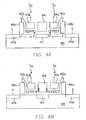
- FIGS. 4A and 4Bare a schematic cross-sectional views of a flash memory cell showing two methods of operating the flash memory cell according to this invention.
- FIG. 4Ashows a method of programming data into the flash memory cell and
- FIG. 4Bshows a method of erasing data from the flash memory cell.
- a bias voltage of about 10Vis applied to the select gate 406 a to open up the channel underneath the select gate 406 a
- a positive bias voltage VCG p within the range 10V to 12Vis applied to the control gate 404 a
- a positive bias voltage VS p of about 6Vis applied to the source region 412 and the drain region 410 a is grounded.
- a bias voltage of about 10Vis applied to the select gate 406 b to open up the channel underneath the select gate 406 b
- a positive bias voltage VCG p within the range 10V to 12Vis applied to the control gate 404 b
- a positive bias voltage VS p of about 6Vis applied to the source region 412 and the drain region 410 b is grounded.
- a 0Vis applied to the control gate 404 a and the control gate 404 b
- a positive bias voltage VSGEwithin the range 10V to 12V is applied to the erase gate 408 and setting the source region 412 , the drain regions 410 a, 410 b in a floating state.
- an intense electric fieldis built up between the floating gates 402 a , 402 b and the erase gate 408 so that electrons are pulled out from the floating gates 402 a , 402 b to the erase gate 408 through the Fowler-Nordheim effect as shown in FIG. 4B.
- an erase gate dielectric layer having a greater thicknesscan be used wile a select gate dielectric layer having a smaller thickness (around 65 ⁇ ) can be used underneath the select gates 406 a , 406 b .
- a smaller threshold voltagecan be used to trigger the memory device and a larger cell current can be used for the programming so that programming disturbance is minimized and operating speed of the memory cell is increased.
- substrate breakdown during an erase operationcan be prevented.
Landscapes
- Non-Volatile Memory (AREA)
Abstract
Description
- 1. Field of Invention[0001]
- The present invention relates to a memory cell device. More particularly, the present invention relates to a flash memory cell structure and a method of manufacturing and operating the memory cell.[0002]
- 2. Description of Related Art[0003]
- Flash memory is a memory device that allows multiple data writing, reading and erasing operations. In addition, the stored data will be retained even after power to the device is removed. With these advantages, it has been broadly applied in personal computers and electronic equipment.[0004]
- A typical flash memory device has a floating gate and a control gate fabricated using doped polysilicon. The control gate is set up above the floating gate with an inter-gate dielectric layer separating the two. Furthermore, a tunneling oxide layer is also set up between the floating gate and an underlying substrate (the so-called stack gate flash memory).[0005]
- To write data into the flash memory, a bias voltage is applied to the control gate and the source/drain regions so that an electric field is set up to inject electrons into the floating gate. On the other hand, to read data from the flash memory, an operating voltage is applied to the control gate. Since the entrapment of charges inside the floating gate will directly affect the opening or closing of the underlying channel, the opening or closing of the channel can be construed as a data value of “1” or “0”. Finally, to erase data from the flash memory, the relative potential between the substrate and the drain (source) region or the control gate is raised. Hence, a tunneling effect can be utilized to transfer electrons from the floating gate to the substrate or drain (source) via the tunneling oxide layer (the so-called substrate erase or drain [source] side erase) or from the floating gate to the control gate via the inter-gate dielectric layer.[0006]
- However, in the process of erasing data from the flash memory, the quantity of electrons expelled from the floating gate is difficult to control and hence often leads to the expulsion of too many electric charges from the floating gate, the so-called over-erasure. When the degree of over-erasure is severe, the channel underneath the floating gate may conduct even before an operating voltage is applied to the control gate. That means, erroneous data value may be read. To lessen the over-erasure problem, many types of flash memories have a split gate design. One major aspect of a split gate design is the inclusion of a select gate (or an erase gate) on the sidewall of the control gate and the floating gate above the substrate. The select gate (or erase gate) is isolated from the control gate, the floating gate and the substrate through an inter-gate dielectric layer. Hence, if the channel underneath the floating gate conducts even without the application of an operating voltage to the control gate due to serious over-erasure, the channel underneath the select gate (or the erase gate) can still be cut off to prevent any electrical connection between the source/drain regions. In other words, erroneous determination of data value can be prevented.[0007]
- FIG. 1 is a schematic cross-sectional view of a conventional split-gate flash memory cell. As shown in FIG. 1, the flash memory cell is fabricated on a[0008]
substrate 100. Atunneling oxide layer 102, afloating gate 104, an inter-gatedielectric layer 106 and acontrol gate 108 are sequentially formed over thesubstrate 100. Aspacer 110 is formed on the sidewalls and top section of thecontrol gate 106 and anotherspacer 112 is formed on the sidewall of thefloating gate 104. Theselect gate 114 is set up on the sidewall on one side of thefloating gate 104 and thecontrol gate 106. A selectgate oxide layer 116 is set up between theselect gate 114 and thesubstrate 100. Asource region 118 is set up in thesubstrate 100 on the side of thefloating gate 104 and thecontrol gate 106 where theselect gate 114 is absent. Thedrain region 120 is set up in thesubstrate 100 on the side of thefloating gate 104 and thecontrol gate 106 where theselect gate 114 is present. - To program the aforementioned flash memory cell, a 10V bias voltage is applied to the[0009]
control gate 108, a 10V bias voltage is applied to theselect gate 114, a 6V bias voltage is applied to thesource region 118 and 0V is applied to thedrain region 120. With this voltage setup, the programming is achieved through the migration of electrons from thedrain region 120 to thesource region 118 and the injection of electrons from thesource region 118 into thefloating gate 104. To erase data from the memory cell, a 0V is applied to thecontrol gate 108 and a 10V to 12V bias voltage is applied to theselect gate 114 while setting thesource region 118 and thedrain region 120 to a floating state. Hence, an electric field of considerable intensity is set up between thefloating gate 104 and theselect gate 114 so that the trapped electrons inside thefloating gate 104 are pulled out and transferred to theselect gate 114 through the Fowler-Nordheim (F-N) tunneling effect. - The aforementioned flash memory cell utilizes the[0010]
select gate 114 both as a channel transistor and an erase gate. In other words, theselect gate 114 serves as an erase gate during an erasing operation. If the select gate oxide layer has only a moderate thickness, substrate breakdown may occur during the erasing operation. Therefore, the selectgate oxide layer 116 must have a thickness capable of preventing a possible substrate breakdown (for example, greater than 200Ã□). However, during a programming operation, theselect gate 114 serves as the gate of a channel transistor. If the selectgate oxide layer 116 is thick, a greater bias voltage will have to be applied to theselect gate 114 just to turn on the channel transistor. In other words, the channel transistor has a high threshold voltage. Furthermore, the cell current flowing from the source terminal to the drain terminal will be reduced leading to a slowdown in the operating speed of the memory cell. On the other hand, if the channel transistor has a low threshold voltage, a greater thickness for the selectgate oxide layer 116 will lead to a worsening of the channel control by the select gate and an increase in substrate leakage current. Since the memory cell has a high programming sensitivity, programming disturbance may occur with greater frequency. - Accordingly, one object of the present invention is to provide a flash memory cell and a method of fabricating and operation the flash memory cell such that current running inside the memory device is increased and programming disturbance within the device is minimized. Hence, overall operating speed of the memory device is improved.[0011]
- To achieve these and other advantages and in accordance with the purpose of the invention, as embodied and broadly described herein, the invention provides a flash memory cell structure. The flash memory cell includes a substrate, a tunneling dielectric layer over the substrate, a floating gate over the tunneling dielectric layer, an inter-gate dielectric layer over the floating gate, a control gate over the inter-gate dielectric layer, a first spacer on the sidewall and the top section of the control gate, a second spacer on the sidewall of the floating gate, a source region in the substrate on a first side of the control gate and the floating gate, an erase gate over a source region, an erase gate dielectric layer between the source region and the erase gate, a select gate on a second side of the control gate and the floating gate, a select gate dielectric layer between the substrate and the select gate and a drain region in the substrate on the side close to the select gate.[0012]
- In the aforementioned flash memory cell, the erase gate dielectric layer has a thickness between about 200Ã□ to 250Ã[0013]58 . The select gate dielectric layer has a thickness between about 50Ã□ to 75Ã□ and the tunneling dielectric layer has a thickness between about 85Ã□ to 110Ã□.
- In this invention, the erase gate is set up over the source region so that separate erase gate and the select gate are used inside the flash memory cell. Hence, the thickness of the select gate dielectric layer can be reduced while the thickness of the erase gate dielectric layer can be increased. Thus, there is no need to apply a high voltage to the select gate when the memory cell is programmed. Furthermore, due to the reduction in thickness of the oxide layer underneath the select gate, memory cell current can be increased when data are read from the memory so that a high operating speed is maintained. In addition, substrate breakdown is also prevented during a memory erase operation.[0014]
- This invention also provides an alternative flash memory cell structure. The flash memory cell includes a substrate, a first gate structure and a second gate structure over the substrate with each gate structure having at least a floating gate over the substrate and a control gate over the floating gate, a source region in the substrate between the first gate structure and the second gate structure, an erase gate above the source region between the first gate structure and the second gate structure, an erase gate dielectric layer between the source region and the erase gate, a first select gate and a second select gate on the sidewall of the first gate structure and the second gate structure away from the source region, a select gate dielectric layer between the substrate and the first and the second select gate and a drain region in the substrate just outside the first select gate and the second select gate.[0015]
- In the aforementioned flash memory cell, the erase gate dielectric layer has a thickness between about 200Ã□ to 250Ã□. The select gate dielectric layer has a thickness between about 50Ã□ to 75Ã□ and the tunneling dielectric layer has a thickness between about 85Ã□ to 110Ã□.[0016]
- In this invention, the erase gate is set up over the source region between the first gate structure and the second gate structure so that separate erase gate and the select gate are used inside the flash memory cell. Hence, the thickness of the select gate dielectric layer can be reduced while the thickness of the erase gate dielectric layer can be increased. Thus, there is no need to apply a high voltage to the select gate when the memory cell is programmed. Furthermore, due to the reduction in thickness of the oxide layer underneath the select gate, memory cell current can be increased when data are read from the memory so that a high operating speed is maintained. In addition, substrate breakdown is also prevented during a memory erase operation. Moreover, with two neighboring gate structures using a single erase gate, there is no increase in the overall size of the flash memory cell.[0017]
- This invention also provides a method of fabricating a flash memory cell. First, a substrate having a first gate structure and a second gate structure thereon is provided. The first gate structure and the second gate structure each includes a tunneling dielectric layer formed over the substrate, a floating gate formed over the tunneling dielectric layer, an inter-gate dielectric layer formed over the floating gate, a control gate formed over the inter-gate dielectric layer and a first spacer formed on the sidewall and top section of the control gate. Thereafter, a source region is formed in the substrate between the first gate structure and the second gate structure. An erase gate dielectric layer is formed over the surface of the source region. A second spacer is formed on the sidewall of the floating gate. An erase gate is formed over the source region such that the erase gate fills up the space between the first gate structure and the second gate structure. After forming a third spacer on the sidewall on one side of the first and the second gate structures, a select gate dielectric layer is formed over the substrate. Next, a first select gate and a second select gate are formed on the sidewall of the third spacers. Finally, a first drain region and a second drain region are formed in the substrate on one side of the first select gate and the second select gate.[0018]
- In the aforementioned method of fabricating the memory cell, the first gate structure and the second gate structure are formed before forming a first dielectric layer, a first conductive layer and a second dielectric layer sequentially over the substrate. Thereafter, a second conductive layer is formed over the second dielectric layer and then the second conductive layer is patterned to form the control gate. Next, a first spacer is formed on the sidewalls and the top section of the control gate. Using the first spacer and the control gate as a mask, the second dielectric layer, the first conductive layer, the first dielectric layer are patterned to form an inter-gate dielectric layer, a floating gate and a tunneling dielectric layer.[0019]
- In this invention, a conductive layer is formed over a source region to fabricate the erase gate so that the erase gate and the select gate are separate devices. Hence, the erase gate dielectric layer can have a greater thickness (for example, greater than 200Ã□) while the select gate dielectric layer underneath the select gate can be thinner (for example, about 65Ã□). As a result, the threshold voltage for triggering the memory device is reduced and cell current flowing inside the memory device is increased. In addition, programming disturbance is minimized so that the memory cell can operate faster. Moreover, with a thicker erase gate dielectric layer, substrate breakdown during an erasing operation is prevented.[0020]
- This invention also provides a method of operating a flash memory cell. The flash memory cell includes a substrate, a floating gate over the substrate, a floating gate over the control gate, a source region in the substrate on a first side of the control gate and the floating gate, an erase gate over the source region on a first side of the control gate and the floating gate, a select gate on the sidewall on a second side of the control gate and the floating gate and a drain region in the substrate on one side of the select gate. The channel hot electron injection effect are induced to program data into the flash memory cell by applying a first positive voltage to the control gate, a second positive voltage to the select gate, a third positive voltage to the source region and maintaining the drain region is in a floating state. The Fowler-Nordheim tunneling effect is induced to erase data from the flash memory cell by applying a fourth positive voltage to the erase gate, setting the control gate to 0V and maintaining both the source region and the drain region in a floating state.[0021]
- In the aforementioned method of operating the flash memory cell, electrons are removed through the erase gate instead of select gate. Hence, the erase gate dielectric layer can have a greater thickness (for example, greater than 200Ã□) while the select gate dielectric layer underneath the select gate can be thinner (for example, about 65Ã□). In other words, a smaller threshold voltage can be used to trigger the memory device and a larger cell current can be used for the programming so that programming disturbance is minimized and operating speed of the memory cell is increased. Furthermore, with a thicker erase dielectric layer, substrate breakdown during an erase operation can be prevented.[0022]
- It is to be understood that both the foregoing general description and the following detailed description are exemplary, and are intended to provide further explanation of the invention as claimed.[0023]
- The accompanying drawings are included to provide a further understanding of the invention, and are incorporated in and constitute a part of this specification. The drawings illustrate embodiments of the invention and, together with the description, serve to explain the principles of the invention.[0024]
- FIG. 1 is a schematic cross-sectional view of a conventional split-gate flash memory cell.[0025]
- FIG. 2 is a schematic cross-sectional view of a flash memory cell according to one preferred embodiment of this invention.[0026]
- FIGS. 3A to[0027]3F are schematic cross-sectional views showing the progression of steps for fabricating a flash memory cell according to one preferred embodiment of this invention.
- FIG. 4A is a schematic cross-sectional view of a flash memory cell showing the method of programming data into the flash memory cell according to this invention.[0028]
- FIG. 4B is a schematic cross-sectional view of a flash memory cell showing the method of erasing data from the flash memory cell according to this invention.[0029]
- Reference will now be made in detail to the present preferred embodiments of the invention, examples of which are illustrated in the accompanying drawings. Wherever possible, the same reference numbers are used in the drawings and the description to refer to the same or like parts.[0030]
- FIG. 2 is a schematic cross-sectional view of a flash memory cell according to one preferred embodiment of this invention. As shown in FIG. 2, the flash memory cell includes a[0031]
substrate 200, agate structure 202, asource region 204, an erasegate 206, an erasegate dielectric layer 208, aspacer 210, aselect gate 212, a selectgate dielectric layer 214 and adrain region 216. - The[0032]
gate structure 202 is set up over thesubstrate 200. Thegate structure 202 includes atunneling oxide layer 218, a floatinggate 220, an inter-gatedielectric layer 222, acontrol gate 224 andspacers gate structures 202 constitutes acomposite gate structure 230. Thetunneling oxide layer 218 is formed over thesubstrate 200. The floating gate is formed over thetunneling oxide layer 218. The inter-gatedielectric layer 222 is formed over the floatinggate 220. Thecontrol gate 224 is formed over the inter-gatedielectric layer 222. Thespacer 226 is formed on the sidewalls and the top section of thecontrol gate 224. Thespacer 228 is formed on the sidewalls of the floatinggate 220. - The[0033]
source region 204 is formed in the substrate200 (in thesubstrate 200 on one side of the gate structure202) within acomposite gate structure 230. The erasegate 206 is formed over thesource region 204 between the two gate structures of thecomposite gate structure 230. The erasegate dielectric layer 208 is formed between the erasegate 206 and thesource region 204. The erasegate dielectric layer 208 having a thickness greater than about 200Ã□ is a silicon oxide layer, for example. Thespacer 210 is formed on the sidewalls of the composite gate structure230 (that is, the sidewall of thegate structure 202 away from the erase gate206). Theselect gate 212 is formed on the sidewall of thespacer 210. The selectgate dielectric layer 212 is formed between theselect gate 212 and thesubstrate 200. The selectgate dielectric layer 212, having a thickness between 50Ã□ to 70Ã□, is a silicon oxide layer, for example. Thedrain region 216 is formed in thesubstrate 200 on one side of theselect gate 212. - In the aforementioned flash memory cell, an additional erase[0034]
gate 206 is set up over thesource region 204 so that the erasegate 206 and theselect gate 212 are separate members. Therefore, thickness of the selectgate dielectric layer 214 underneath theselect gate 212 can be reduced while the erasegate dielectric layer 208 underneath the erasegate 206 can be increased. As a result, a smaller voltage can be applied to theselect gate 212 to program data into the memory cell at a normal operating speed and substrate breakdown during a memory erasing operation can be prevented. Moreover, with each pair of neighboring gate structures202 (memory cells) using the same erasegate 206, there is no additional size increase in the memory cell of this invention. - FIGS. 3A to[0035]3F are schematic cross-sectional views showing the progression of steps for fabricating a flash memory cell according to one preferred embodiment of this invention. As shown in FIG. 3A, a
substrate 300 is provided. Thereafter, atunneling dielectric layer 302 is formed over thesubstrate 300. Thetunneling dielectric layer 302 is a silicon oxide layer formed, for example, by performing a thermal oxidation process. Thetunneling dielectric layer 302 preferably has a thickness between about 85Ã□˜110Ã□. - Thereafter, a[0036]
conductive layer 304 is formed over the tunnelingdielectric layer 302. Theconductive layer 304 is a doped polysilicon layer formed, for example, by performing a chemical vapor deposition process to form an undoped polysilicon layer and then performing an ion implantation process to transformed the undoped polysilicon layer into the doped polysilicon layer. Theconductive layer 304 preferably has a thickness about 200Ã□. Arsenic ions, for example, are used to form the implantedconductive layer 204 so that easy-to-erase circular structures are formed in a subsequent thermal oxidation process. Next, an inter-gatedielectric layer 306 is formed over thesubstrate 300. The inter-gatedielectric layer 306 is, for example, an oxide/nitride/oxide composite layer with the lower oxide layer having a thickness between 60Ã□ to 100Ã□, the middle nitride layer having a thickness between 70Ã□ to 100Ã□ and the upper oxide layer having a thickness between 60Ã□ to 100Ã□. To form the inter-gatedielectric layer 306, for example, a thermal oxidation process is performed to form a silicon oxide layer over thesubstrate 300. Thereafter, a chemical vapor deposition process is performed to deposit a silicon nitride layer over the silicon oxide layer. Finally, a wet hydrogen/oxygen (H2/O2) gaseous mixture is blown over the nitride layer to oxidize a portion of the nitride layer into another silicon oxide layer over the nitride layer. Obviously, the inter-gatedielectric layer 306 can be a silicon oxide layer or an oxide/nitride composite layer as well. - As shown in FIG. 3B, a conductive layer (not shown) is formed over the[0037]
substrate 300. Thereafter, using a mask, the conductive layer is patterned to form aconductive layer 308 that serves as a control gate. Theconductive layer 308 is a doped polysilicon layer formed, for example, by performing a chemical vapor deposition process with in-situ ion doping. After removing the mask, an insulating layer310 (a spacer) is formed on the sidewalls and the top section of theconductive layer 308. The insulating layer310 (the spacer) is a silicon oxide layer formed, for example, by performing a thermal oxidation process. - As shown in FIG. 3C, using the[0038]
conductive layer 308 and the insulating layer310 (the spacer) as a mask, the inter-gatedielectric layer 306, theconductive layer 304 and thetunneling dielectric layer 302 are patterned to form an inter-gatedielectric layer 306a,aconductive layer 304aand atunneling dielectric layer 302a. Theconductive layer 304aserves as a floating gate. The conductive layer (the control gate)308, the inter-gatedielectric layer 306a,the conductive layer (the floating gate)304aand the oxide layer302 (the tunneling oxide layer) together form agate structure 311. Thereafter, a patternedmask layer 312 is formed over thesubstrate 300 globally. The patternedmask layer 312 exposes a portion of thesubstrate 300 for forming asource region 314. Using the patternedmask layer 312 as a mask, an ion implantation is carried out implanting dopants into thesubstrate 300 to form thesource region 314. In general, each pair of neighboringgate structures 311 can be regarded as a composite gate so that thesource region 314 is located between theindividual gate structure 311 of the pair. - As shown in FIG. 3D, the patterned[0039]
mask layer 312 is removed. Thereafter, an erasegate dielectric layer 316 is formed over thesource region 314 between twogate structures 311, adielectric layer 318 is formed over thesubstrate 300 and an insulating layer (a spacer)320 is formed on the sidewall of theconductive layer 304a(the floating gate). The erasegate dielectric layer 316, thedielectric layer 318 and the insulating layer (the spacer)320 are silicon oxide layers formed, for example, by performing a thermal oxidation process. The erasegate oxide layer 316 has a thickness greater than 200Ã□, preferably between about 200Ã□ to 250Ã□. Next, aconductive layer 322 is formed over the source region314 (that is, between the gate structures311). Theconductive layer 322 serves as an erase gate. Theconductive layer 322 is a doped polysilicon layer formed, for example, by performing a chemical vapor deposition process with in-situ ion doping to form a conductive layer (not shown) over thesubstrate 300 and then removing excess conductive material outside the space between thegate structures 311. - As shown in FIG. 3E, a[0040]
spacer 324 is formed on the sidewall of thegate structure 311 away from theconductive layer 322. Thespacer 324 is formed, for example, by forming a high temperature oxide (HTO) having a thickness between 150Ã□ to 400Ã□ and then performing an anisotropic etching process to remove a portion of the HTO layer. Only a portion of thedielectric layer 318 is retained to form adielectric layer 318awhen thespacer 324 is formed. However, thedielectric layer 318acan be regarded as a portion of thespacer 324. Thereafter, a selectgate dielectric layer 326 is formed over thesubstrate 300 and then an insulatinglayer 328 is formed on the top section of theconductive layer 322. The selectgate dielectric layer 326 is a silicon oxide layer having a thickness between 50Ã□ to 70Ã□, for example. The selectgate dielectric layer 326 and the insulatinglayer 328 are formed, for example, by performing a thermal oxidation process. - As shown in FIG. 3F, a[0041]
conductive layer 330 is formed on the sidewall of thegate structures 311 away from theconductive layer 322. Theconductive layer 320 is a doped polysilicon layer formed, for example, by performing a chemical vapor deposition process with in-situ ion doping to form a conductive layer (not shown) over thesubstrate 300 and then performing an anisotropic etching process to remove a portion of the conductive layer. Thereafter, using thegate structures 311 and theconductive layers 330 as a mask, an ion implantation is carried out implanting dopants into thesubstrate 300 to form a drain region332 on one side of theconductive layer 330. Finally, other operations necessary for completing the flash memory cell fabrication are carried through. Since conventional processes are used, a detailed description of these operations is omitted here. - In the aforementioned embodiment of this invention, a[0042]
conductive layer 322 is formed over asource region 314 to fabricate the erase gate so that the erase gate and the select gate are separate devices. Hence, the erasegate dielectric layer 316 can have a greater thickness (for example, greater than 200Ã□) while the selectgate dielectric layer 326 underneath the select gate can be thinner (for example, about 65Ã□). As a result, threshold voltage for triggering the memory device is reduced and cell current flowing inside the memory device is increased. In addition, programming disturbance is minimized so that the memory cell can operate faster. Moreover, with a thicker erase gate dielectric layer, substrate breakdown during an erasing operation is prevented. - FIGS. 4A and 4B are a schematic cross-sectional views of a flash memory cell showing two methods of operating the flash memory cell according to this invention. FIG. 4A shows a method of programming data into the flash memory cell and FIG. 4B shows a method of erasing data from the flash memory cell.[0043]
- To program the memory cell Qn[0044]1, for example, a bias voltage of about 10V is applied to the
select gate 406ato open up the channel underneath theselect gate 406a,a positive bias voltage VCGpwithin the range 10V to 12V is applied to thecontrol gate 404a,a positive bias voltage VSpof about 6V is applied to thesource region 412 and thedrain region 410ais grounded. With this voltage setup, electrons move from thedrain region 410ato thesource region 412 and get accelerated by the high channel field at thesource region 412 terminal to produce hot electrons. Thus, the electrons received enough kinetic energy to overcome the energy barrier of the tunneling dielectric layer. Together with the positive bias voltage applied to thecontrol gate 404a, the hot electrons are injected from thesource region 412 terminal into the floatinggate 402aand hence programmed the memory cell Qn1. Similarly, to program the memory cell Qn2, a bias voltage of about 10V is applied to theselect gate 406bto open up the channel underneath theselect gate 406b,a positive bias voltage VCGpwithin the range 10V to 12V is applied to thecontrol gate 404b,a positive bias voltage VSpof about 6V is applied to thesource region 412 and thedrain region 410bis grounded. With this voltage setup, electrons move from thedrain region 410bto thesource region 412 and are accelerated by the high channel field at thesource region 412 terminal to produce hot electrons. Thus, the electrons received enough kinetic energy to overcome the energy barrier of the tunneling dielectric layer. Together with the positive bias voltage applied to thecontrol gate 404b,the hot electrons are injected from thesource region 412 terminal into the floatinggate 402band hence programmed the memory cell Qn2. - To erase data from the memory cells Qn[0045]1, Qn2, a 0V is applied to the
control gate 404aand thecontrol gate 404b,a positive bias voltage VSGE within the range 10V to 12V is applied to the erasegate 408 and setting thesource region 412, thedrain regions gates gate 408 so that electrons are pulled out from the floatinggates gate 408 through the Fowler-Nordheim effect as shown in FIG. 4B. - In the aforementioned embodiment, electrons are removed by way of the erase[0046]
gate 408 instead of theselect gate 406aor theselect gate 406b.Hence, an erase gate dielectric layer having a greater thickness (greater than 200Ã□) can be used wile a select gate dielectric layer having a smaller thickness (around 65Ã□) can be used underneath theselect gates - It will be apparent to those skilled in the art that various modifications and variations can be made to the structure of the present invention without departing from the scope or spirit of the invention. In view of the foregoing, it is intended that the present invention cover modifications and variations of this invention provided they fall within the scope of the following claims and their equivalents.[0047]
Claims (20)
1. A flash memory cell, comprising:
a substrate;
a tunneling dielectric layer formed over the substrate;
a floating gate formed over the tunneling dielectric layer;
an inter-gate dielectric layer formed over the floating gate;
a control gate formed over the inter-gate dielectric layer;
a first spacer layer formed on the sidewalls and the top section of the control gate;
a pair of second spacers formed on the sidewalls of the floating gate;
a source region formed in the substrate on a first side of the control gate and the floating gate;
an erase gate formed on the source region;
an erase gate dielectric layer formed between the source region and the erase gate;
a select gate formed on a second side of the control gate and the floating gate;
a select gate dielectric layer formed between the substrate and the select gate; and
a drain region formed in the substrate on one side of the select gate.
2. The flash memory cell ofclaim 1 , wherein the erase gate dielectric layer has a thickness between about 200Ã□ to 250Ã□.
3. The flash memory cell ofclaim 1 , wherein the select gate dielectric layer has a thickness between about 50Ã□ to 75Ã□.
4. The flash memory cell ofclaim 1 , wherein the tunneling dielectric layer has a thickness between about 85Ã□ to 110Ã□.
5. The flash memory cell ofclaim 1 , wherein the cell further comprises a third spacer formed between the select gate and the control gate as well as between the select gate and the floating gate.
6. A flash memory cell, comprising:
a substrate;
a first gate structure and a second gate structure formed on the substrate, wherein the first gate structure and the second gate structure each has at least a floating gate formed over the substrate and a control gate formed over the floating gate;
a source region formed in the substrate between the first gate structure and the second gate structure;
an erase gate formed above the source region between the first gate structure and the second gate structure;
an erase gate dielectric layer formed between the source region and the erase gate;
a first select gate and a second select gate formed on one side of the sidewall of the first gate structure and the second gate structure away from the source region;
a select gate dielectric layer formed between the substrate and the first and second select gate; and
a pair of drain regions formed in the substrate just outside the first select gate and the second select gate.
7. The flash memory cell ofclaim 6 , wherein the erase gate dielectric layer has a thickness between about 200Ã□ to 250Ã□.
8. The flash memory cell ofclaim 6 , wherein the select gate dielectric layer has a thickness between about 50Ã□ to 75Ã□.
9. The flash memory cell ofclaim 6 , wherein each of the first gate structure and the second gate structure further comprises:
a tunneling dielectric layer formed between the floating gate and the substrate;
an inter-gate dielectric layer formed between the control gate and the floating gate;
a first spacer layer formed on the sidewalls and the top section of the control gate; and
a pair of second spacers formed on the sidewalls of the floating gate.
10. The flash memory cell ofclaim 9 , wherein the tunneling dielectric layer has a thickness between about 85Ã□ to 110Ã□.
11. A method of fabricating flash memory cells, comprising the steps of:
providing a substrate, wherein the substrate has a first gate structure and a second gate structure thereon, the first gate structure and the second gate structure each comprises a tunneling dielectric layer formed over the substrate, a floating gate formed over the tunneling dielectric layer, an inter-gate dielectric layer formed over the floating gate, a control gate formed over the inter-gate dielectric layer and a first spacer formed on the sidewalls and the top section of the control gate;
forming a source region in the substrate between the first gate structure and the second gate structure;
forming an erase gate dielectric layer over the upper surface of the source region and forming a second spacer on the sidewalls of the floating gate;
forming an erase gate over the source region such that the erase gate completely fills the space between the first gate structure and the second gate structure;
forming third spacers on the other sides of the first gate structure and the second gate structure corresponding the erase gate;
forming a select gate dielectric layer over the substrate;
forming a first select gate and a second select gate on the sidewall of the third spacers; and
forming a first drain region and a second drain region in the substrate just outside the first select gate and the second select gate.
12. The method ofclaim 11 , wherein the step of forming the first gate structure and the second gate structure furthermore includes:
forming a first dielectric layer over the substrate;
forming a first conductive layer over the dielectric layer;
forming a second dielectric layer over the first conductive layer;
forming a second conductive layer over the second dielectric layer;
patterning the second conductive layer to form the control gate;
forming the first spacer layer on the sidewalls and the top section of the control gate; and
patterning the second dielectric layer, the first conductive layer, the first dielectric layer to form the inter-gate dielectric layer, the floating gate and the tunneling dielectric layer using the first spacer layer and the control gate as a mask.
13. The method ofclaim 11 , wherein the step of forming the erase gate dielectric layer over the source region and a pair of second spacers on the sidewalls of the floating gate includes performing a thermal oxidation process.
14. The method ofclaim 11 , wherein the erase gate dielectric layer has a thickness between about 200Ã□ to 250Ã□.
15. The method ofclaim 11 , wherein the select gate dielectric layer has a thickness between about 50Ã□ to 75Ã□.
16. The method ofclaim 11 , wherein the tunneling dielectric layer has a thickness between about 85Ã□ to 110Ã□.
17. The method ofclaim 11 , wherein the step of forming the select gate dielectric layer over the substrate further comprises a step of forming an insulating layer over the erase gate.
18. The method ofclaim 17 , wherein the step of forming the select gate dielectric layer over the substrate comprises performing a thermal oxidation process.
19. The method ofclaim 11 , wherein the floating gate includes arsenic doped polysilicon layer.
20. A method of operating a flash memory cell, wherein the flash memory cell comprises a substrate, a floating gate formed over the substrate, a control gate formed over the floating gate, a source region formed in the substrate on a first side of the control gate and the floating gate, an erase gate formed above the source region on the firs side of the control gate and the floating gate, a select gate formed on a second side of the sidewall of the control gate and the floating gate, a drain region formed in the substrate just outside the select gate, the operating method comprising the steps of:
applying a first positive voltage to the control gate, applying a second positive voltage to the select gate, applying a third positive voltage to the source region and connecting the drain region to ground so that channel hot electrons are injected to program data into the flash memory cell; and
applying a fourth positive voltage to the erase gate, setting the control gate to 0V and setting the source region and the drain region to a floating state so that the Fowler-Nordheim effect is triggered to erase data from the flash memory cell.
Priority Applications (1)
| Application Number | Priority Date | Filing Date | Title |
|---|---|---|---|
| US10/250,286US20040256657A1 (en) | 2003-06-20 | 2003-06-20 | [flash memory cell structure and method of manufacturing and operating the memory cell] |
Applications Claiming Priority (1)
| Application Number | Priority Date | Filing Date | Title |
|---|---|---|---|
| US10/250,286US20040256657A1 (en) | 2003-06-20 | 2003-06-20 | [flash memory cell structure and method of manufacturing and operating the memory cell] |
Publications (1)
| Publication Number | Publication Date |
|---|---|
| US20040256657A1true US20040256657A1 (en) | 2004-12-23 |
Family
ID=33516816
Family Applications (1)
| Application Number | Title | Priority Date | Filing Date |
|---|---|---|---|
| US10/250,286AbandonedUS20040256657A1 (en) | 2003-06-20 | 2003-06-20 | [flash memory cell structure and method of manufacturing and operating the memory cell] |
Country Status (1)
| Country | Link |
|---|---|
| US (1) | US20040256657A1 (en) |
Cited By (29)
| Publication number | Priority date | Publication date | Assignee | Title |
|---|---|---|---|---|
| US20060203552A1 (en)* | 2004-03-17 | 2006-09-14 | Actrans System Incorporation, Usa | Process of Fabricating Flash Memory with Enhanced Program and Erase Coupling |
| US20060237761A1 (en)* | 2005-04-26 | 2006-10-26 | Ming-Chang Kuo | Non-volatile memory, fabrication method thereof and operation method thereof |
| US20070042544A1 (en)* | 2005-08-16 | 2007-02-22 | Macronix International Co., Ltd. | Low-k spacer structure for flash memory |
| JP2009044164A (en)* | 2007-08-06 | 2009-02-26 | Silicon Storage Technology Inc | Improved split-gate non-volatile flash memory cell, array, and fabrication method having a floating gate, a control gate, a select gate, and an erase gate with an overhang on the floating gate |
| US20100165736A1 (en)* | 2008-12-31 | 2010-07-01 | Young Jun Kwon | Flash memory device and manufacturing method of the same |
| US20110006355A1 (en)* | 2009-07-08 | 2011-01-13 | Taiwan Semiconductor Manufacturing Company, Ltd. | Novel Structure for Flash Memory Cells |
| US20120201084A1 (en)* | 2011-02-04 | 2012-08-09 | Taiwan Semiconductor Manufacturing Company, Ltd. | Operating methods of flash memory and decoding circuits thereof |
| CN102637694A (en)* | 2012-04-05 | 2012-08-15 | 上海华力微电子有限公司 | Stacked gate type programmable flash memory device |
| US8320191B2 (en) | 2007-08-30 | 2012-11-27 | Infineon Technologies Ag | Memory cell arrangement, method for controlling a memory cell, memory array and electronic device |
| CN103715144A (en)* | 2012-09-29 | 2014-04-09 | 中芯国际集成电路制造(上海)有限公司 | Discrete gate memory device and forming method thereof |
| US20150263123A1 (en)* | 2014-03-13 | 2015-09-17 | Taiwan Semiconductor Manufacturing Co., Ltd. | Common source oxide formation by in-situ steam oxidation for embedded flash |
| US20150364558A1 (en)* | 2014-06-17 | 2015-12-17 | Taiwan Semiconductor Manufacturing Co., Ltd. | Split gate flash memory structure and method of making the split gate flash memory structure |
| CN105514043A (en)* | 2015-02-16 | 2016-04-20 | 北京芯盈速腾电子科技有限责任公司 | Non-volatile memory manufacturing method and non-volatile memory |
| US20160336415A1 (en)* | 2015-05-15 | 2016-11-17 | Taiwan Semiconductor Manufacturing Co., Ltd. | Memory cell structure for improving erase speed |
| US9583640B1 (en)* | 2015-12-29 | 2017-02-28 | Globalfoundries Inc. | Method including a formation of a control gate of a nonvolatile memory cell and semiconductor structure |
| US20170162589A1 (en)* | 2013-01-10 | 2017-06-08 | Micron Technology, Inc. | Transistors, Semiconductor Constructions, and Methods of Forming Semiconductor Constructions |
| US9865693B1 (en)* | 2016-08-04 | 2018-01-09 | United Microelectronics Corporation | Semiconductor memory cell, semiconductor memory device, and method of manufacturing semiconductor memory device |
| KR20180060946A (en)* | 2016-11-29 | 2018-06-07 | 타이완 세미콘덕터 매뉴팩쳐링 컴퍼니 리미티드 | Semiconductor device and manufacturing method thereof |
| US20190067305A1 (en)* | 2017-08-29 | 2019-02-28 | Taiwan Semiconductor Manufacturing Company Ltd. | Semiconductor structure for memory device and method for forming the same |
| CN109712981A (en)* | 2019-01-02 | 2019-05-03 | 上海华虹宏力半导体制造有限公司 | Memory and forming method thereof |
| US20190140099A1 (en)* | 2017-11-08 | 2019-05-09 | Globalfoundries Singapore Pte. Ltd. | Split gate non-volatile memory (nvm) with improved programming efficiency |
| US20190145927A1 (en)* | 2015-12-07 | 2019-05-16 | Taiwan Semiconductor Manufacturing Co., Ltd. | Dual gate biologically sensitive field effect transistor |
| US20190148529A1 (en)* | 2016-04-20 | 2019-05-16 | Silicon Storage Technology, Inc. | Method Of Forming Pairs Of Three-Gate Non-volatile Flash Memory Cells Using Two Polysilicon Deposition Steps |
| US10325918B2 (en) | 2016-11-29 | 2019-06-18 | Taiwan Semiconductor Manufacturing Co., Ltd. | Semiconductor device and manufacturing method thereof |
| US10340393B2 (en) | 2013-01-07 | 2019-07-02 | Micron Technology, Inc. | Semiconductor constructions, methods of forming vertical memory strings, and methods of forming vertically-stacked structures |
| CN111180447A (en)* | 2018-11-09 | 2020-05-19 | 物联记忆体科技股份有限公司 | Nonvolatile memory and method of manufacturing the same |
| US10950611B2 (en) | 2016-11-29 | 2021-03-16 | Taiwan Semiconductor Manufacturing Co., Ltd. | Semiconductor device and manufacturing method thereof |
| CN115643761A (en)* | 2022-10-31 | 2023-01-24 | 北京知存科技有限公司 | Preparation process of flash memory cell array and flash memory cell array |
| CN119233639A (en)* | 2024-11-13 | 2024-12-31 | 上海华力集成电路制造有限公司 | Manufacturing method of SONOS memory |
Citations (3)
| Publication number | Priority date | Publication date | Assignee | Title |
|---|---|---|---|---|
| US5756385A (en)* | 1994-03-30 | 1998-05-26 | Sandisk Corporation | Dense flash EEPROM cell array and peripheral supporting circuits formed in deposited field oxide with the use of spacers |
| US6573142B1 (en)* | 2002-02-26 | 2003-06-03 | Taiwan Semiconductor Manufacturing Company | Method to fabricate self-aligned source and drain in split gate flash |
| US6747310B2 (en)* | 2002-10-07 | 2004-06-08 | Actrans System Inc. | Flash memory cells with separated self-aligned select and erase gates, and process of fabrication |
- 2003
- 2003-06-20USUS10/250,286patent/US20040256657A1/ennot_activeAbandoned
Patent Citations (3)
| Publication number | Priority date | Publication date | Assignee | Title |
|---|---|---|---|---|
| US5756385A (en)* | 1994-03-30 | 1998-05-26 | Sandisk Corporation | Dense flash EEPROM cell array and peripheral supporting circuits formed in deposited field oxide with the use of spacers |
| US6573142B1 (en)* | 2002-02-26 | 2003-06-03 | Taiwan Semiconductor Manufacturing Company | Method to fabricate self-aligned source and drain in split gate flash |
| US6747310B2 (en)* | 2002-10-07 | 2004-06-08 | Actrans System Inc. | Flash memory cells with separated self-aligned select and erase gates, and process of fabrication |
Cited By (62)
| Publication number | Priority date | Publication date | Assignee | Title |
|---|---|---|---|---|
| US7718488B2 (en)* | 2004-03-17 | 2010-05-18 | Silicon Storage Technology, Inc. | Process of fabricating flash memory with enhanced program and erase coupling |
| US20060203552A1 (en)* | 2004-03-17 | 2006-09-14 | Actrans System Incorporation, Usa | Process of Fabricating Flash Memory with Enhanced Program and Erase Coupling |
| US20060237761A1 (en)* | 2005-04-26 | 2006-10-26 | Ming-Chang Kuo | Non-volatile memory, fabrication method thereof and operation method thereof |
| US7170129B2 (en)* | 2005-04-26 | 2007-01-30 | Macronix International Co., Ltd. | Non-volatile memory, fabrication method thereof and operation method thereof |
| US20070092997A1 (en)* | 2005-04-26 | 2007-04-26 | Macronix International Co., Ltd. | Fabrication method of non-volatile memory |
| US7732256B2 (en)* | 2005-04-26 | 2010-06-08 | Macronix International Co., Ltd. | Fabrication method of non-volatile memory |
| US7846794B2 (en) | 2005-08-16 | 2010-12-07 | Macronix International Co., Ltd. | Low-K spacer structure for flash memory |
| US20070042544A1 (en)* | 2005-08-16 | 2007-02-22 | Macronix International Co., Ltd. | Low-k spacer structure for flash memory |
| US7319618B2 (en)* | 2005-08-16 | 2008-01-15 | Macronic International Co., Ltd. | Low-k spacer structure for flash memory |
| US20080076219A1 (en)* | 2005-08-16 | 2008-03-27 | Macronix International Co., Ltd. | Low-K Spacer Structure for Flash Memory |
| JP2009044164A (en)* | 2007-08-06 | 2009-02-26 | Silicon Storage Technology Inc | Improved split-gate non-volatile flash memory cell, array, and fabrication method having a floating gate, a control gate, a select gate, and an erase gate with an overhang on the floating gate |
| US8320191B2 (en) | 2007-08-30 | 2012-11-27 | Infineon Technologies Ag | Memory cell arrangement, method for controlling a memory cell, memory array and electronic device |
| US9030877B2 (en) | 2007-08-30 | 2015-05-12 | Infineon Technologies Ag | Memory cell arrangement, method for controlling a memory cell, memory array and electronic device |
| US20100165736A1 (en)* | 2008-12-31 | 2010-07-01 | Young Jun Kwon | Flash memory device and manufacturing method of the same |
| US8264030B2 (en)* | 2008-12-31 | 2012-09-11 | Dongbu Hitek Co., Ltd. | Flash memory device and manufacturing method of the same |
| US20110006355A1 (en)* | 2009-07-08 | 2011-01-13 | Taiwan Semiconductor Manufacturing Company, Ltd. | Novel Structure for Flash Memory Cells |
| US8445953B2 (en)* | 2009-07-08 | 2013-05-21 | Taiwan Semiconductor Manufacturing Company, Ltd. | Structure for flash memory cells |
| US9257568B2 (en) | 2009-07-08 | 2016-02-09 | Taiwan Semiconductor Manufacturing Company, Ltd. | Structure for flash memory cells |
| US8908434B2 (en)* | 2011-02-04 | 2014-12-09 | Taiwan Semiconductor Manufacturing Company, Ltd. | Operating methods of flash memory and decoding circuits thereof |
| US20120201084A1 (en)* | 2011-02-04 | 2012-08-09 | Taiwan Semiconductor Manufacturing Company, Ltd. | Operating methods of flash memory and decoding circuits thereof |
| CN102637694A (en)* | 2012-04-05 | 2012-08-15 | 上海华力微电子有限公司 | Stacked gate type programmable flash memory device |
| CN103715144A (en)* | 2012-09-29 | 2014-04-09 | 中芯国际集成电路制造(上海)有限公司 | Discrete gate memory device and forming method thereof |
| US10340393B2 (en) | 2013-01-07 | 2019-07-02 | Micron Technology, Inc. | Semiconductor constructions, methods of forming vertical memory strings, and methods of forming vertically-stacked structures |
| US10833205B2 (en) | 2013-01-07 | 2020-11-10 | Micron Technology, Inc. | Semiconductor constructions, methods of forming vertical memory strings, and methods of forming vertically-stacked structures |
| US11424256B2 (en) | 2013-01-10 | 2022-08-23 | Micron Technology, Inc. | Transistors, semiconductor constructions, and methods of forming semiconductor constructions |
| US10497707B2 (en)* | 2013-01-10 | 2019-12-03 | Micron Technology, Inc. | Semiconductor constructions which include metal-containing gate portions and semiconductor-containing gate portions |
| US20170162589A1 (en)* | 2013-01-10 | 2017-06-08 | Micron Technology, Inc. | Transistors, Semiconductor Constructions, and Methods of Forming Semiconductor Constructions |
| US20150263123A1 (en)* | 2014-03-13 | 2015-09-17 | Taiwan Semiconductor Manufacturing Co., Ltd. | Common source oxide formation by in-situ steam oxidation for embedded flash |
| US9679980B2 (en)* | 2014-03-13 | 2017-06-13 | Taiwan Semiconductor Manufacturing Co., Ltd. | Common source oxide formation by in-situ steam oxidation for embedded flash |
| US20150364558A1 (en)* | 2014-06-17 | 2015-12-17 | Taiwan Semiconductor Manufacturing Co., Ltd. | Split gate flash memory structure and method of making the split gate flash memory structure |
| US9614048B2 (en)* | 2014-06-17 | 2017-04-04 | Taiwan Semiconductor Manufacturing Co., Ltd. | Split gate flash memory structure and method of making the split gate flash memory structure |
| CN105514043A (en)* | 2015-02-16 | 2016-04-20 | 北京芯盈速腾电子科技有限责任公司 | Non-volatile memory manufacturing method and non-volatile memory |
| US9917165B2 (en)* | 2015-05-15 | 2018-03-13 | Taiwan Semiconductor Manufacturing Co., Ltd. | Memory cell structure for improving erase speed |
| US20160336415A1 (en)* | 2015-05-15 | 2016-11-17 | Taiwan Semiconductor Manufacturing Co., Ltd. | Memory cell structure for improving erase speed |
| US12352724B2 (en) | 2015-12-07 | 2025-07-08 | Taiwan Semiconductor Manufacturing Co., Ltd. | Dual gate biologically sensitive field effect transistor |
| US11614422B2 (en) | 2015-12-07 | 2023-03-28 | Taiwan Semiconductor Manufacturing Co., Ltd. | Dual gate biologically sensitive field effect transistor |
| US20190145927A1 (en)* | 2015-12-07 | 2019-05-16 | Taiwan Semiconductor Manufacturing Co., Ltd. | Dual gate biologically sensitive field effect transistor |
| US10876998B2 (en)* | 2015-12-07 | 2020-12-29 | Taiwan Semiconductor Manufacturing Co., Ltd. | Dual gate biologically sensitive field effect transistor |
| US9583640B1 (en)* | 2015-12-29 | 2017-02-28 | Globalfoundries Inc. | Method including a formation of a control gate of a nonvolatile memory cell and semiconductor structure |
| US11652162B2 (en) | 2016-04-20 | 2023-05-16 | Silicon Storage Technology, Inc. | Method of forming a three-gate non-volatile flash memory cell using two polysilicon deposition steps |
| US20190148529A1 (en)* | 2016-04-20 | 2019-05-16 | Silicon Storage Technology, Inc. | Method Of Forming Pairs Of Three-Gate Non-volatile Flash Memory Cells Using Two Polysilicon Deposition Steps |
| US9865693B1 (en)* | 2016-08-04 | 2018-01-09 | United Microelectronics Corporation | Semiconductor memory cell, semiconductor memory device, and method of manufacturing semiconductor memory device |
| KR20180060946A (en)* | 2016-11-29 | 2018-06-07 | 타이완 세미콘덕터 매뉴팩쳐링 컴퍼니 리미티드 | Semiconductor device and manufacturing method thereof |
| US10950611B2 (en) | 2016-11-29 | 2021-03-16 | Taiwan Semiconductor Manufacturing Co., Ltd. | Semiconductor device and manufacturing method thereof |
| US12439594B2 (en) | 2016-11-29 | 2025-10-07 | Taiwan Semiconductor Manufacturing Company, Ltd. | Semiconductor device and manufacturing method thereof |
| US12058856B2 (en) | 2016-11-29 | 2024-08-06 | Taiwan Semiconductor Manufacturing Company, Ltd. | Semiconductor device and manufacturing method thereof |
| US11825651B2 (en) | 2016-11-29 | 2023-11-21 | Taiwan Semiconductor Manufacturing Company, Ltd. | Semiconductor device and manufacturing method thereof |
| CN108172580A (en)* | 2016-11-29 | 2018-06-15 | 台湾积体电路制造股份有限公司 | Semiconductor device and manufacturing method thereof |
| US10879253B2 (en) | 2016-11-29 | 2020-12-29 | Taiwan Semiconductor Manufacturing Co., Ltd. | Semiconductor device and manufacturing method thereof |
| US10943996B2 (en) | 2016-11-29 | 2021-03-09 | Taiwan Semiconductor Manufacturing Co., Ltd. | Method of manufacturing semiconductor device including non-volatile memories and logic devices |
| US10950715B2 (en) | 2016-11-29 | 2021-03-16 | Taiwan Semiconductor Manufacturing Co., Ltd. | Method of manufacturing semiconductor device including non-volatile memories and logic devices |
| KR102112114B1 (en)* | 2016-11-29 | 2020-05-19 | 타이완 세미콘덕터 매뉴팩쳐링 컴퍼니 리미티드 | Semiconductor device and manufacturing method thereof |
| US10325918B2 (en) | 2016-11-29 | 2019-06-18 | Taiwan Semiconductor Manufacturing Co., Ltd. | Semiconductor device and manufacturing method thereof |
| US11594620B2 (en) | 2016-11-29 | 2023-02-28 | Taiwan Semiconductor Manufacturing Co., Ltd. | Semiconductor device and manufacturing method thereof |
| US10879250B2 (en)* | 2017-08-29 | 2020-12-29 | Taiwan Semiconductor Manufacturing Company Ltd. | Semiconductor structure for memory device and method for forming the same |
| US20190067305A1 (en)* | 2017-08-29 | 2019-02-28 | Taiwan Semiconductor Manufacturing Company Ltd. | Semiconductor structure for memory device and method for forming the same |
| US20190140099A1 (en)* | 2017-11-08 | 2019-05-09 | Globalfoundries Singapore Pte. Ltd. | Split gate non-volatile memory (nvm) with improved programming efficiency |
| US10347773B2 (en)* | 2017-11-08 | 2019-07-09 | Globalfoundries Singapore Pte. Ltd. | Split gate non-volatile memory (NVM) with improved programming efficiency |
| CN111180447A (en)* | 2018-11-09 | 2020-05-19 | 物联记忆体科技股份有限公司 | Nonvolatile memory and method of manufacturing the same |
| CN109712981A (en)* | 2019-01-02 | 2019-05-03 | 上海华虹宏力半导体制造有限公司 | Memory and forming method thereof |
| CN115643761A (en)* | 2022-10-31 | 2023-01-24 | 北京知存科技有限公司 | Preparation process of flash memory cell array and flash memory cell array |
| CN119233639A (en)* | 2024-11-13 | 2024-12-31 | 上海华力集成电路制造有限公司 | Manufacturing method of SONOS memory |
Similar Documents
| Publication | Publication Date | Title |
|---|---|---|
| US20040256657A1 (en) | [flash memory cell structure and method of manufacturing and operating the memory cell] | |
| US5614747A (en) | Method for manufacturing a flash EEPROM cell | |
| JP3733595B2 (en) | Manufacturing method of semiconductor device including MOS element | |
| US20080198669A1 (en) | Method of operating non-volatile memory | |
| JP2882392B2 (en) | Nonvolatile semiconductor memory device and method of manufacturing the same | |
| US6875660B2 (en) | Method of manufacturing high coupling ratio flash memory having sidewall spacer floating gate electrode | |
| US6943404B2 (en) | Sonos multi-level memory cell | |
| US5422292A (en) | Process for fabricating split gate flash EEPROM memory | |
| US5643812A (en) | Method of making EEPROM flash memory cell with erase gate | |
| US5756384A (en) | Method of fabricating an EPROM cell with a high coupling ratio | |
| US6245614B1 (en) | Method of manufacturing a split-gate flash memory cell with polysilicon spacers | |
| US7397080B2 (en) | Non-volatile memory | |
| KR100348311B1 (en) | Nonvolatile Memory Device and method for Fabricating the same | |
| US7164177B2 (en) | Multi-level memory cell | |
| KR20040023294A (en) | Method for fabricating non-volatile memory device having a sidewall gate and SONOS(Silicon-Oxide-Nitride-Oxide-Silicon) cell structure | |
| KR100606928B1 (en) | Nonvolatile Memory Device and Manufacturing Method Thereof | |
| US6025229A (en) | Method of fabricating split-gate source side injection flash memory array | |
| US20080293200A1 (en) | Method of fabricating nonvolatile semiconductor memory device | |
| JP4969748B2 (en) | Nonvolatile semiconductor memory device and method of manufacturing nonvolatile memory cell | |
| TWI555131B (en) | Nor flash memory and manufacturing method thereof | |
| US7220651B2 (en) | Transistor and method for manufacturing the same | |
| KR100606536B1 (en) | Nonvolatile Memory Device and Manufacturing Method Thereof | |
| US7227216B2 (en) | Mono gate memory device and fabricating method thereof | |
| CN100372121C (en) | Multi-level memory cell | |
| CN1534785A (en) | Flash memory unit, manufacturing method of flash memory unit and operation method of flash memory unit |
Legal Events
| Date | Code | Title | Description |
|---|---|---|---|
| AS | Assignment | Owner name:POWERCHIP SEMICONDUCTOR CORP., TAIWAN Free format text:ASSIGNMENT OF ASSIGNORS INTEREST;ASSIGNORS:HUNG, CHIH-WEI;HSU, CHENG-YUAN;WU, CHI-SHAN;AND OTHERS;REEL/FRAME:013744/0106 Effective date:20030502 | |
| STCB | Information on status: application discontinuation | Free format text:ABANDONED -- FAILURE TO RESPOND TO AN OFFICE ACTION |