US20040256647A1 - Strained silicon finFET device - Google Patents
Strained silicon finFET deviceDownload PDFInfo
- Publication number
- US20040256647A1 US20040256647A1US10/602,436US60243603AUS2004256647A1US 20040256647 A1US20040256647 A1US 20040256647A1US 60243603 AUS60243603 AUS 60243603AUS 2004256647 A1US2004256647 A1US 2004256647A1
- Authority
- US
- United States
- Prior art keywords
- silicon
- layer
- channel
- strained
- seed
- Prior art date
- Legal status (The legal status is an assumption and is not a legal conclusion. Google has not performed a legal analysis and makes no representation as to the accuracy of the status listed.)
- Granted
Links
- XUIMIQQOPSSXEZ-UHFFFAOYSA-NSiliconChemical compound[Si]XUIMIQQOPSSXEZ-UHFFFAOYSA-N0.000titleclaimsabstractdescription389
- 229910052710siliconInorganic materials0.000titleclaimsabstractdescription378
- 239000010703siliconSubstances0.000titleclaimsabstractdescription377
- 229910000577Silicon-germaniumInorganic materials0.000claimsabstractdescription177
- LEVVHYCKPQWKOP-UHFFFAOYSA-N[Si].[Ge]Chemical compound[Si].[Ge]LEVVHYCKPQWKOP-UHFFFAOYSA-N0.000claimsabstractdescription155
- OKTJSMMVPCPJKN-UHFFFAOYSA-NCarbonChemical compound[C]OKTJSMMVPCPJKN-UHFFFAOYSA-N0.000claimsabstractdescription42
- 229910052799carbonInorganic materials0.000claimsabstractdescription42
- 239000000758substrateSubstances0.000claimsdescription103
- 238000000034methodMethods0.000claimsdescription70
- 239000012212insulatorSubstances0.000claimsdescription67
- 239000000463materialSubstances0.000claimsdescription41
- 238000004519manufacturing processMethods0.000claimsdescription32
- 238000000151depositionMethods0.000claimsdescription20
- 238000000059patterningMethods0.000claimsdescription14
- 125000006850spacer groupChemical group0.000claimsdescription10
- 229910052732germaniumInorganic materials0.000claimsdescription8
- GNPVGFCGXDBREM-UHFFFAOYSA-Ngermanium atomChemical compound[Ge]GNPVGFCGXDBREM-UHFFFAOYSA-N0.000claimsdescription8
- 230000015572biosynthetic processEffects0.000claimsdescription4
- 125000001475halogen functional groupChemical group0.000claimsdescription3
- 238000002513implantationMethods0.000claimsdescription3
- FGUUSXIOTUKUDN-IBGZPJMESA-NC1(=CC=CC=C1)N1C2=C(NC([C@H](C1)NC=1OC(=NN=1)C1=CC=CC=C1)=O)C=CC=C2Chemical compoundC1(=CC=CC=C1)N1C2=C(NC([C@H](C1)NC=1OC(=NN=1)C1=CC=CC=C1)=O)C=CC=C2FGUUSXIOTUKUDN-IBGZPJMESA-N0.000claims1
- 230000000694effectsEffects0.000abstractdescription13
- 230000009467reductionEffects0.000abstractdescription4
- 230000002708enhancing effectEffects0.000abstract1
- 239000010410layerSubstances0.000description258
- 230000008569processEffects0.000description44
- VYPSYNLAJGMNEJ-UHFFFAOYSA-NSilicium dioxideChemical compoundO=[Si]=OVYPSYNLAJGMNEJ-UHFFFAOYSA-N0.000description29
- 239000004065semiconductorSubstances0.000description25
- 230000008021depositionEffects0.000description17
- 235000012239silicon dioxideNutrition0.000description12
- 239000000377silicon dioxideSubstances0.000description12
- 229910003811SiGeCInorganic materials0.000description11
- 235000012431wafersNutrition0.000description11
- 238000005530etchingMethods0.000description10
- 230000003647oxidationEffects0.000description9
- 238000007254oxidation reactionMethods0.000description9
- 229920002120photoresistant polymerPolymers0.000description9
- 229910021332silicideInorganic materials0.000description7
- FVBUAEGBCNSCDD-UHFFFAOYSA-Nsilicide(4-)Chemical compound[Si-4]FVBUAEGBCNSCDD-UHFFFAOYSA-N0.000description7
- 238000005468ion implantationMethods0.000description6
- 238000000206photolithographyMethods0.000description6
- 230000006872improvementEffects0.000description5
- 229910021420polycrystalline siliconInorganic materials0.000description5
- 229920005591polysiliconPolymers0.000description5
- 229910052814silicon oxideInorganic materials0.000description5
- 229910052581Si3N4Inorganic materials0.000description4
- 230000008901benefitEffects0.000description4
- 150000001875compoundsChemical class0.000description4
- 238000005520cutting processMethods0.000description4
- 230000005669field effectEffects0.000description4
- 230000004048modificationEffects0.000description4
- 238000012986modificationMethods0.000description4
- HQVNEWCFYHHQES-UHFFFAOYSA-Nsilicon nitrideChemical compoundN12[Si]34N5[Si]62N3[Si]51N64HQVNEWCFYHHQES-UHFFFAOYSA-N0.000description4
- 229910045601alloyInorganic materials0.000description3
- 239000000956alloySubstances0.000description3
- 239000002019doping agentSubstances0.000description3
- 230000003071parasitic effectEffects0.000description3
- 238000001020plasma etchingMethods0.000description3
- PXHVJJICTQNCMI-UHFFFAOYSA-NNickelChemical compound[Ni]PXHVJJICTQNCMI-UHFFFAOYSA-N0.000description2
- BPQQTUXANYXVAA-UHFFFAOYSA-NOrthosilicateChemical compound[O-][Si]([O-])([O-])[O-]BPQQTUXANYXVAA-UHFFFAOYSA-N0.000description2
- KDLHZDBZIXYQEI-UHFFFAOYSA-NPalladiumChemical compound[Pd]KDLHZDBZIXYQEI-UHFFFAOYSA-N0.000description2
- NRTOMJZYCJJWKI-UHFFFAOYSA-NTitanium nitrideChemical compound[Ti]#NNRTOMJZYCJJWKI-UHFFFAOYSA-N0.000description2
- YKTSYUJCYHOUJP-UHFFFAOYSA-N[O--].[Al+3].[Al+3].[O-][Si]([O-])([O-])[O-]Chemical compound[O--].[Al+3].[Al+3].[O-][Si]([O-])([O-])[O-]YKTSYUJCYHOUJP-UHFFFAOYSA-N0.000description2
- 239000004020conductorSubstances0.000description2
- 230000007547defectEffects0.000description2
- 230000008570general processEffects0.000description2
- 229910052735hafniumInorganic materials0.000description2
- VBJZVLUMGGDVMO-UHFFFAOYSA-Nhafnium atomChemical compound[Hf]VBJZVLUMGGDVMO-UHFFFAOYSA-N0.000description2
- 229910000449hafnium oxideInorganic materials0.000description2
- WIHZLLGSGQNAGK-UHFFFAOYSA-Nhafnium(4+);oxygen(2-)Chemical compound[O-2].[O-2].[Hf+4]WIHZLLGSGQNAGK-UHFFFAOYSA-N0.000description2
- 239000007943implantSubstances0.000description2
- 229910052751metalInorganic materials0.000description2
- 239000002184metalSubstances0.000description2
- TWNQGVIAIRXVLR-UHFFFAOYSA-Noxo(oxoalumanyloxy)alumaneChemical compoundO=[Al]O[Al]=OTWNQGVIAIRXVLR-UHFFFAOYSA-N0.000description2
- RVTZCBVAJQQJTK-UHFFFAOYSA-Noxygen(2-);zirconium(4+)Chemical compound[O-2].[O-2].[Zr+4]RVTZCBVAJQQJTK-UHFFFAOYSA-N0.000description2
- 239000003870refractory metalSubstances0.000description2
- 229910001928zirconium oxideInorganic materials0.000description2
- GFQYVLUOOAAOGM-UHFFFAOYSA-Nzirconium(iv) silicateChemical compound[Zr+4].[O-][Si]([O-])([O-])[O-]GFQYVLUOOAAOGM-UHFFFAOYSA-N0.000description2
- 206010010144Completed suicideDiseases0.000description1
- RYGMFSIKBFXOCR-UHFFFAOYSA-NCopperChemical compound[Cu]RYGMFSIKBFXOCR-UHFFFAOYSA-N0.000description1
- 229910000881Cu alloyInorganic materials0.000description1
- 108091006149Electron carriersProteins0.000description1
- ZOKXTWBITQBERF-UHFFFAOYSA-NMolybdenumChemical compound[Mo]ZOKXTWBITQBERF-UHFFFAOYSA-N0.000description1
- 238000001015X-ray lithographyMethods0.000description1
- HMDDXIMCDZRSNE-UHFFFAOYSA-N[C].[Si]Chemical compound[C].[Si]HMDDXIMCDZRSNE-UHFFFAOYSA-N0.000description1
- 229910052782aluminiumInorganic materials0.000description1
- XAGFODPZIPBFFR-UHFFFAOYSA-NaluminiumChemical compound[Al]XAGFODPZIPBFFR-UHFFFAOYSA-N0.000description1
- WPPDFTBPZNZZRP-UHFFFAOYSA-Naluminum copperChemical compound[Al].[Cu]WPPDFTBPZNZZRP-UHFFFAOYSA-N0.000description1
- 230000015556catabolic processEffects0.000description1
- 229910017052cobaltInorganic materials0.000description1
- 239000010941cobaltSubstances0.000description1
- GUTLYIVDDKVIGB-UHFFFAOYSA-Ncobalt atomChemical compound[Co]GUTLYIVDDKVIGB-UHFFFAOYSA-N0.000description1
- 229910052802copperInorganic materials0.000description1
- 239000010949copperSubstances0.000description1
- 239000013078crystalSubstances0.000description1
- 230000003247decreasing effectEffects0.000description1
- 238000006731degradation reactionMethods0.000description1
- 230000002939deleterious effectEffects0.000description1
- 238000005137deposition processMethods0.000description1
- 239000003989dielectric materialSubstances0.000description1
- 238000009792diffusion processMethods0.000description1
- 230000009977dual effectEffects0.000description1
- 238000000609electron-beam lithographyMethods0.000description1
- 239000011521glassSubstances0.000description1
- 238000007654immersionMethods0.000description1
- 239000012535impuritySubstances0.000description1
- 239000011810insulating materialSubstances0.000description1
- 230000003993interactionEffects0.000description1
- 150000002500ionsChemical class0.000description1
- 230000007774longtermEffects0.000description1
- 229910052750molybdenumInorganic materials0.000description1
- 239000011733molybdenumSubstances0.000description1
- 229910021421monocrystalline siliconInorganic materials0.000description1
- 229910052759nickelInorganic materials0.000description1
- 229910052763palladiumInorganic materials0.000description1
- 230000008439repair processEffects0.000description1
- XUIMIQQOPSSXEZ-AKLPVKDBSA-Nsilicon-31 atomChemical compound[31Si]XUIMIQQOPSSXEZ-AKLPVKDBSA-N0.000description1
- 239000007787solidSubstances0.000description1
- 230000001629suppressionEffects0.000description1
- 239000002344surface layerSubstances0.000description1
- 229910021341titanium silicideInorganic materials0.000description1
- 230000005641tunnelingEffects0.000description1
Images


Classifications
- H—ELECTRICITY
- H10—SEMICONDUCTOR DEVICES; ELECTRIC SOLID-STATE DEVICES NOT OTHERWISE PROVIDED FOR
- H10D—INORGANIC ELECTRIC SEMICONDUCTOR DEVICES
- H10D30/00—Field-effect transistors [FET]
- H10D30/60—Insulated-gate field-effect transistors [IGFET]
- H10D30/62—Fin field-effect transistors [FinFET]
- H—ELECTRICITY
- H10—SEMICONDUCTOR DEVICES; ELECTRIC SOLID-STATE DEVICES NOT OTHERWISE PROVIDED FOR
- H10D—INORGANIC ELECTRIC SEMICONDUCTOR DEVICES
- H10D30/00—Field-effect transistors [FET]
- H10D30/01—Manufacture or treatment
- H10D30/021—Manufacture or treatment of FETs having insulated gates [IGFET]
- H10D30/024—Manufacture or treatment of FETs having insulated gates [IGFET] of fin field-effect transistors [FinFET]
- H—ELECTRICITY
- H10—SEMICONDUCTOR DEVICES; ELECTRIC SOLID-STATE DEVICES NOT OTHERWISE PROVIDED FOR
- H10D—INORGANIC ELECTRIC SEMICONDUCTOR DEVICES
- H10D30/00—Field-effect transistors [FET]
- H10D30/60—Insulated-gate field-effect transistors [IGFET]
- H10D30/67—Thin-film transistors [TFT]
- H10D30/674—Thin-film transistors [TFT] characterised by the active materials
- H10D30/6741—Group IV materials, e.g. germanium or silicon carbide
- H10D30/6748—Group IV materials, e.g. germanium or silicon carbide having a multilayer structure or superlattice structure
- H—ELECTRICITY
- H10—SEMICONDUCTOR DEVICES; ELECTRIC SOLID-STATE DEVICES NOT OTHERWISE PROVIDED FOR
- H10D—INORGANIC ELECTRIC SEMICONDUCTOR DEVICES
- H10D30/00—Field-effect transistors [FET]
- H10D30/60—Insulated-gate field-effect transistors [IGFET]
- H10D30/751—Insulated-gate field-effect transistors [IGFET] having composition variations in the channel regions
Definitions
- This inventionrelated generally to semiconductor devices including field effect transistors (FETs), metal-oxide-semiconductor FETs (MOSFETs), and more particularly related to improved semiconductor devices having double gates and strained channel.
- FETsfield effect transistors
- MOSFETsmetal-oxide-semiconductor FETs
- FETsField effect transistors
- MOSFETsMetal-Oxide-Semiconductor field effect transistors
- MOSFET devicesexperience certain deleterious performance due to their size, such as the short channel effect caused by the close proximity of the source and drain, resulting in the reduction of the threshold voltage and the increase of sub-threshold current.
- the source and drain regionsmay extend towards each other and may essentially occupy the entire channel area between the source and the drain.
- the channelis in part depleted and the gate charge necessary to alter the source and drain current flow is reduced.
- the interaction between the source and drain of the MOSFETdegrades the ability of the gate to control the operation of the device.
- ultra thin gate dielectricequivalent oxide thickness should be less than 0.5 nm
- ultra shallow junctionless than 10 nm depth for reducing short channel effect
- high concentration channel doping>10 18 cm ⁇ 3
- ultra thin gate oxideless than 1-2 nm
- ultra shallow junctionhas significant problem of low sheet resistance and junction lateral steepness.
- Silicon-On-Insulator (SOI) substratehas enabled MOSFET devices to have higher speed, lower power and higher density.
- Strain-induced band modification of the device channelhas enabled MOSFET devices to have enhanced carrier mobility and therefore increased drive current.
- Double gate MOSFET structureallows gate control of the channel from both sides, reducing short channel effect and allowing more current flow.
- Double gate MOSFET structureoffers improvement for short channel effect reduction since it adds another gate on either side of the channel to allow gate control of the channel from both sides. Additionally, when the device is turned on using both gates, two conduction layers are formed, allowing more current flow. An extension of the double gate is the wrap-around gate where the gate is surrounding the channel.
- One variation of double gate MOSFET structureis finFET, a double gate device consists of a silicon channel formed in a silicon vertical fin controlled by a self-aligned double gate.
- the epitaxial layerwill try to extend itself to match the larger lattice constant, and therefore experience tensile stress and forming a tensile strained channel fin structure. If the lattice constant of the seed fin is smaller than the lattice constant of the epitaxial layer, the epitaxial layer will try squeeze itself into the smaller lattice constant, and therefore experience compressive stress and forming a compressive strained channel fin structure.
- the strained silicon fin channelcomprises an epitaxial silicon layer deposited on a relaxed silicon germanium seed fin.
- Other embodiments of the inventioninclude an epitaxial silicon layer deposited on a strained silicon germanium seed fin wherein the strained silicon germanium seed fin is deposited on an underseed relaxed silicon layer, and a strained channel silicon fin fabricated on a relaxed silicon germanium seed layer.
- the present invention strained silicon channel fin structurecan be employed to fabricate a strained silicon finFET device.
- the present invention strained silicon finFET devicecomprises a thin strained silicon-containing fin channel standing on an insulator layer, sandwiching between a source and a drain.
- a gate dielectric and double gatescover the sides of the fin to form the inversion layers on the sides of the channel.
- the channel finis sufficiently thin so that the two gates control the entire channel film.
- the double gates on the channel fincan suppress the short channel effect and enhance drive current.
- the strained channelcan provide enhanced carrier mobility to further improve the device performance.
- the present invention strained channel finFET devicethus can improve hole carrier mobility and/or electron carrier mobility, in addition to suppressing short channel effect.
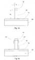
- FIG. 1shows an embodiment of the present invention strained silicon channel fin structure.
- FIG. 2shows a variation of the embodiment of FIG. 1.
- FIGS. 3 a - 3 cshow the fabrication process of the embodiment of FIG. 1.
- FIGS. 4 a - 4 cshow the fabrication process of the embodiment of FIG. 2.
- FIG. 5shows another embodiment of the present invention strained silicon channel fin structure.
- FIGS. 8 a - 8 cshow the fabrication process of the embodiment of FIG. 6.
- FIG. 9shows another embodiment of the present invention strained silicon channel fin structure.
- FIGS. 12 a - 12 bshow the fabrication process of the embodiment of FIG. 10.
- FIG. 14shows different views of an embodiment of the disclosed strained silicon finFET device.
- FIGS. 18 a - 18 eshow the fabrication steps of the strained silicon finFET device in accordance with one embodiment of the invention.
- the present invention strained silicon fin structurecomprises a seed fin structure disposed on an insulator substrate, and a strained channel layer fabricated on the seed fin structure.
- the channel layer materialhas a lattice constant different than the lattice constant of the seed fin material, and therefore the channel layer becomes a strained channel layer due the lattice mismatch between the seed fin and the channel layer.
- FIG. 1An embodiment of the present invention strained silicon fin structure is shown in FIG. 1 wherein the channel layer covers both the top side and the two sidewalls of the seed fin.
- the seed fin of this embodimentcan be a strained seed fin, but preferably a relaxed seed fin.
- a strained channel silicon layer 11covers a relaxed silicon germanium fin seed fin 10 on an insulator layer 12 .
- the relaxed silicon germanium fin 10is preferably disposed on an insulator layer 12 (such as silicon dioxide) on a silicon substrate 13 .
- the seed fin 10is a relaxed silicon germanium fin having lattice constant larger than the lattice constant of silicon, therefore the epitaxial silicon layer 11 grown on the seed fin 10 will be tensilely strained.
- the relaxed silicon germanium fin structureis preferably fabricated from a silicon germanium-on-insulator (SGOI) substrate with the concentration of germanium ranging from 10% to 100%. Then the SGOI substrate is patterned into a silicon germanium fin structure. Then a silicon layer is epitaxially deposited on the silicon germanium fin structure. The epitaxial deposition is preferably selectively epitaxial deposition wherein the deposition only occurs on the silicon germanium exposed surfaces.
- the siliconis under biaxial tensile stress because the lattice constant of silicon is smaller than the lattice constant of silicon germanium. The degree of tensile stress is a function of the concentration of germanium and can be optimized for the desired properties of the silicon device.
- the patterning of the silicon germanium fin from the SGOI substrateis preferably by photolithography where a patterned mask is provided on the substrate, then the substrate is patterned according to the pattern mask, and then the patterned mask is removed.
- the patterned maskis preferably a photoresist layer, coated and exposed to UV light under a photo mask to transfer a pattern from the photo mask onto the photoresist.
- the photoresist maskprotects the substrate during an etch step to transfer the pattern from the photoresist onto the substrate. And then the photoresist mask can be stripped.
- the pattern transfer etchingis preferably accomplished by reactive ion etching or by wet etches.
- SGOI substratesbelong to a class of Silicon-On-Insulator (SOI) substrates.
- SOI substratetypically consists of a thin surface layer of single crystal silicon on an underlayer of insulating material on a bulk silicon wafer.
- the thin surface silicon layertypically a few tens of nanometers to several microns thick, is the silicon channel of the transistor.
- the insulating layerusually made of silicon dioxide, is referred to as the buried oxide and is usually a few hundreds of nanometers thick.
- the present inventionis not limited to just silicon, but applicable to various silicon-containing materials or semiconductor materials such as silicon germanium, silicon carbon, or compound semiconductor materials.
- silicon in “strained silicon fin structure” and “strained silicon finFET device”can mean silicon germanium, carbon doped silicon, or other semiconductor material.
- SOI used in the present inventionis also broadened to include all substrates having a thin semiconductor layer on an insulator on a semiconductor substrate. Examples include a silicon layer on a silicon dioxide insulating layer on a silicon substrate (SOI), and a silicon germanium layer on a silicon dioxide insulating layer on a silicon substrate (SGOI). Other example is a carbon doped silicon layer on a silicon dioxide insulating layer on a silicon substrate.
- the insulator substrate used in the present inventionmeans a substrate having a multilayer on an insulator on a semiconductor support layer.
- the multilayercan comprise 2 or more semiconductor layers having mismatched lattice constants so that the upper semiconductor layer can be under strain.
- the bottommost layer of the multilayeris generally a part of the wafer substrate, such as a silicon layer in a SOI substrate, or a silicon germanium layer in a SGOI substrate.
- the upper layers of the multilayercan be epitaxially deposited on the bottommost layer of the SOI or SGOI wafer.
- the multilayercan also comprise a plurality of semiconductor layers and a hard mask layer.
- the term SOI substrate in the present inventionalso covers all substrates having similar structures (semiconductor/insulator/semiconductor) such as SIMOX substrates.
- FIG. 2shows a variation of the above strained silicon fin structure with the addition of a hard mask layer on the seed fin structure.
- the channel layercover only the two sidewalls of the seed fin structure.
- the epitaxial silicon layer 11 ′only deposited on the silicon germanium exposed sidewall surfaces, and not on the top of the seed fin.
- the strained silicon channel fin structure as shown in FIG. 2can become double gate device in a finFET structure because the silicon channel covers only two sides of the seed fin structure.
- the epitaxial channel silicon layer 11 or 11 ′ grown on the relaxed silicon germanium seed fin 10will be tensilely strained because the lattice constant of silicon is smaller than that of silicon germanium. Due to this tensile strain, the six-fold degeneracy of the electron conduction band of the silicon layer is split into a two-fold degenerate band and a four-fold degenerate band. The two-fold degenerate band has smaller energy, and therefore the electrons have smaller effective mass in this band, resulting in the electrons moving faster in the strained silicon channel of the silicon germanium/silicon heterojunction. Thus the mobility of the electrons in the strained silicon channel increases, resulting in the increased speed of the operating transistor.
- the silicon germanium/silicon heterojunctionserves as a heterobarrier to confine the electrons in the silicon channel.
- the tensile strain of the silicon layeralso serves to split the two-fold degeneracy valence band into a light hole band and a heavy hole band. Similar to the case of the conduction band, the light hole band has smaller energy, resulting in smaller effective mass of the holes, and an increase in hole mobility in the strained silicon channel device.
- the channel layeris an epitaxial carbon doped silicon (SiC) layer or an epitaxial carbon doped silicon germanium (SiGeC) layer. Since the lattice constant of carbon is smaller than the lattice constant of silicon or germanium, carbon doped silicon layer or carbon doped silicon germanium layer fabricated on the silicon germanium seed fin will be tensilely strained, and thus forming a strained carbon doped silicon or a carbon doped silicon germanium fin structure. The concentration of carbon in the carbon doped silicon or silicon germanium is preferably less than 30%.
- strained SiC or SiGeC channel layerSimilar to strained silicon channel mobility enhancement, the degeneracy of the conduction and valence bands in the SiC and SiGeC layer is similarly split, resulting in an enhancement of electron and hole mobility of the strained SiC and SiGeC channel layer.
- a further advantage of strained SiC or SiGeC channel layeris that the energy level of the light hole band is higher, and thus the light holes can also be confined in the strained SiC or SiGeC channel layer, similar to and in addition to the confinement of the light electrons.
- a further advantage of the strained SiC or SiGeC channel layeris that the seed fin can be silicon.
- a variation of the above embodimentcomprises a SiC or SiGeC channel layer fabricated on a silicon seed fin.
- SOIsilicon-on-insulator
- the silicon germanium layershould be grown on the silicon substrate until the silicon germanium becomes thick enough to reduce the lattice strain of the silicon germanium layer.
- the lattice strain of the silicon germaniumis relaxed, a large number of dislocations can be generated in the silicon germanium layer. These dislocations may deteriorate the performance characteristics of the transistor and its long-term reliability.
- Better technologyis currently available to reduce the defect level in SGOI substrates, but in general, SOI substrates are more technologically advanced.
- the starting substrate of the above embodimentis a relaxed silicon germanium layer 15 on an insulator 12 on a silicon substrate 13 (SiGe-On-Insulator, SGOI) (FIG. 3 a ).
- a fin structureis patterned on the SGOI substrate.
- the patterning of the silicon germanium finis preferably by photolithography process.
- the silicon germanium fin structure 10 after the patterning processis shown in FIG. 3 b with a thickness T and height H.
- FIG. 3 bshows the etching of the silicon germanium layer 15 and stopping on the insulator layer 12 , but the pattern etching of the fin structure may be over-etched onto the insulator layer 12 .
- the fabrication processcontinues with a selective deposition of an epitaxial silicon layer 11 , covering the exposed surface of the silicon germanium (FIG. 3 c ). Due to the mismatched lattice constants between the silicon germanium seed fin structure and the epitaxial deposited silicon layer, the deposited silicon layer is under strained to form a strained silicon fin structure.
- a hard mask 16can be first deposited on the silicon germanium layer 15 to form a multilayer 16 / 15 on an insulator 12 on a silicon substrate 13 (FIG. 4 a ). Then the fabrication process continues as above with the patterning of a fin structure comprising a hard mask section 14 on a silicon germanium fin section 10 (FIG. 4 b ) with a thickness T and height H, and the selective epitaxial deposition of a silicon layer 11 ′ (FIG. 4 c ). Since the hard mask is preferably an insulator material such as silicon dioxide or silicon nitride, the selective deposition of the silicon layer only deposited on the two sides of the seed fin structure. The hard mask then can be etched away, or left alone to protect the fin structure during subsequent process steps.
- the complete fin structure after FIG. 4 bwill be similar to the fin structure shown in FIG. 3 c.
- FIG. 5shows the embodiment of the present invention strained silicon channel fin structure with the strained seed fin disposed on an underseed layer.
- the strained channel silicon 21covers the strained silicon germanium fin seed layer 20 on a relaxed silicon underseed layer 25 on an insulator layer 22 .
- the relaxed silicon underseed layer 25is preferably disposed on an insulator layer 12 (such as silicon dioxide) on a silicon substrate 23 .
- the silicon-on-insulator substrateis patterned into a multilayer seed fin structure.
- the multilayeris silicon germanium on silicon, preferably fabricated by epitaxially deposition of a layer of silicon germanium on a SOI substrate.
- the multilayercomprises 2 semiconductor layers (silicon germanium layer and silicon layer) having mismatched lattice constant to generate the strained in the upper silicon germanium layer. Then a silicon channel layer 21 is epitaxially deposited on the multilayer fin seed structure.
- the epitaxial depositionis preferably selectively epitaxial deposition wherein the deposition only occurs on the silicon germanium or silicon surface.
- the seed fin structurehas a thickness of T and a height of H as shown in FIG. 5.
- the silicon underseed layer 25has a relaxed silicon lattice d Si because of the SOI substrate.
- the epitaxial silicon layer deposited on the strained silicon germanium seed layerwill experience some strain.
- the silicon germaniummight experience some lattice shrinkage in the z direction, but in general, the silicon germanium is rigid enough to prevent serious lattice shrinkage, and the lattice constant of the deposited silicon germanium in the z direction could still be larger than the relaxed silicon germanium lattice constant.
- the epitaxial deposited silicon layerwill have the lattice constant x′ Si , y′ Si and z′ Si in the x, y, and z directions respectively.
- y′ Siy Si (the relaxed silicon lattice constant) in the y direction
- z′ Siz SiGe (the tensile strained silicon germanium lattice constant, larger than the relaxed silicon lattice constant) in the z direction.
- the lattice constant of the epitaxial deposited silicon layer in the x direction x′ Sican be smaller or larger than the relaxed silicon lattice constant d Si .
- the epitaxial silicon layercould be under tensile strained in the z direction due to the silicon germanium seed.
- the silicon germanium layeris preferably having a concentration of germanium ranging from 10% to 100%, and more preferably from 10% to 50%.
- FIG. 6shows a variation of the above strained silicon channel fin structure. If a hard mask 24 was used and left on the seed fin before the selective epitaxial deposition of the silicon layer, the silicon 21 ′ only deposited on the silicon germanium 20 and silicon 25 exposed surface, and not on the top of the seed fin.
- the epitaxial layeris an epitaxial carbon doped silicon (SiC) layer or an epitaxial carbon doped silicon germanium (SiGeC) layer. Since the lattice constant of carbon is smaller than the lattice constant of silicon or germanium, carbon doped silicon layer or carbon doped silicon germanium layer fabricated on the silicon germanium seed layer will have a tensile strain, and thus forming a strained carbon doped silicon or a carbon doped silicon germanium fin structure.
- Fabrication process of the above embodimentcan start on a silicon layer 26 on an insulator 22 on a silicon substrate 23 (Si-On-Insulator, SOI wafer).
- the thickness of the silicon layeris preferably between 5 nm to 20 nm, therefore a thinning process can be applied if the silicon thickness of the starting SOI wafer is outside of this range.
- a preferred thinning processis to oxidize the silicon layer and then wet etch the silicon oxide layer. Then a silicon germanium layer 27 is deposited on the silicon layer 26 (FIG. 7 a ).
- FIG. 7 asilicon germanium layer
- a silicon on insulator substratein which a silicon-containing multilayer (in this case, a silicon germanium/silicon multilayer) is disposed on an insulator layer. Due to the mismatched lattices between silicon and silicon germanium, the silicon germanium layer 27 is under lattice strained.
- a fin structureis then patterned on the silicon germanium/silicon substrate. The patterning of the silicon germanium/silicon fin is preferably by photolithography process.
- the fin structureconsists of a silicon germanium seed fin 20 on a silicon underseed 25 is shown in FIG. 7 b.
- the pattern etching of the fin structuremay be over-etched onto the insulator layer 22 , or onto the silicon substrate 23 .
- the fabrication processcontinues with a selective deposition of an epitaxial silicon layer 21 , covering the exposed surface of the silicon germanium and silicon (FIG. 7 c ). Due to the mismatched lattice constants between the strained silicon germanium seed fin structure and the epitaxial deposited silicon layer, the deposited silicon layer is under strained to form a strained silicon fin structure.
- FIG. 8 ais a silicon on insulator substrate in which a silicon-containing multilayer (in this case, a hard mask/silicon germanium/silicon multilayer) is disposed on an insulator layer. Then the fabrication process continues as above with the patterning of a fin structure comprising a hard mask section 24 on a silicon germanium fin section 20 on a silicon underseed section 25 (FIG. 8 b ), and the selective epitaxial deposition of a silicon layer 21 ′ (FIG. 8 c ).
- a silicon-containing multilayerin this case, a hard mask/silicon germanium/silicon multilayer
- the hard maskis preferably an insulator material such as silicon dioxide or silicon nitride, the selective deposition of the silicon layer only deposited on the two sides of the seed fin structure. The hard mask then can be etched away, or left alone to protect the fin structure during subsequent process steps.
- the complete fin structure after FIG. 8 bwill be similar to the fin structure shown in FIG. 7 c.
- strained silicon channel fin structurehas the channel layer covering only the top side of the seed fin.
- the seed fin of this embodimentcan be a strained seed fin, but preferably a relaxed seed fin.
- the strained channel materialis carbon doped silicon (SiC) or carbon doped silicon germanium (SiGeC).
- the seed layeris a silicon layer of a SOI substrate.
- the strained channelcan be silicon germanium, carbon doped silicon (SiC) or carbon doped silicon germanium (SiGeC).
- the channel film width in a finFET deviceis less than channel length, and the double gates on the channel fin effectively suppress short channel effect and enhance drive current.
- Self-aligned gates in which the two gates are self-aligned to each other and to the source and drain regionsare preferred for reducing parasitic gate capacitance, series resistance and for control of the channel length.
- the disclosed strained silicon finFET devicecan further have raised source and drain to reduce parasitic resistance. Since the fin is thin, doping of the fin is not required to suppress short channel effect and undoped silicon can be used as device channel, reducing mobility degradation due to impurity scattering.
- the strained silicon finFET structureis preferably fabricated on an insulator substrate such as a silicon-on-insulator (SOI) substrate. It is also possible that the disclosed strained silicon finFET device is fabricated on a bulk semiconductor substrate such as a bulk silicon wafer.
- SOIsilicon-on-insulator
- Various embodiments of the seed fin and the overlaid channel layer having mismatch latticesare:
- an epitaxial channel layer deposited on a seed finfor example
- an epitaxial channel layer deposited on a seed fin with the seed fin fabricated on an underseed layerfor example
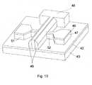
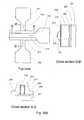
- FIG. 14shows the top view of the disclosed strained silicon finFET device having the first embodiment of a silicon layer on a seed fin structure without a hard mask.
- the finFETis a field effect transistor having a source 106 and a drain 107 separated by a channel 104 .
- the channel 104 conductionis controlled by the double gate 103 , extending and covering the channel 104 , and connected to the gate electrode 108 .
- the double gate 103is electrically isolated from the channel 104 by a spacer 109 and a gate dielectric 110 .
- the double gate 103is actually a triple gate because it covers both sides and the top of the strained silicon channel 104 .
- the term “double gate” in the context of the present inventionis a generic term to mean “more than one gate”, and therefore covers double or triple gate device.
- FIG. 14also shows the cross section AA′, cutting through the fin channel 104 of the finFET structure.
- the finFET deviceis preferably fabricated on an insulator layer 102 on a substrate 101 .
- the finFET channelis a strained silicon channel, comprising a seed fin 105 and a strained silicon channel 104 , covering both sides and the top of the seed fin 105 .
- the finFET devicebecomes a triple gate device because the gate 103 covers the strained silicon channel 104 on both sides and also on the top of the fin.
- the triple gate 103is isolated from the channel 104 by a gate dielectric 110 .
- FIG. 14further shows the cross section BB′, cutting through the triple gate 103 of the finFET structure.
- the cross section BB′cuts through the seed fin layer 105 on a insulator layer 102 and a substrate 101 , the strained silicon channel 104 and the gate dielectric 110 .
- the triple gate 103also covers the top section of the fin structure, with the spacer 109 to isolate the triple gate 103 from the silicon channel 104 .
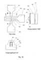
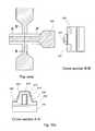
- FIG. 15shows the cross section AA′, cutting through the fin channel 104 of the new variation finFET structure.
- the finFET channelis a strained silicon channel, comprising a seed fin 105 , a hard mask 111 and a strained silicon channel 104 selectively grown on the seed fin 105 .
- the double gate 103covers the strained silicon channel 104 and is isolated from the channel 104 by a gate dielectric 110 .
- FIG. 16shows the cross section AA′ for another embodiment of the finFET structure having a silicon layer on a seed fin structure with the seed fin structure generated from a underseed layer.
- the finFET deviceis fabricated on an insulator layer 122 on a substrate 121 .
- the finFET channelis a strained silicon channel, comprising a seed fin 125 grown on an underseed layer 132 , and a strained silicon channel 124 selectively grown on the seed fin 125 and the underseed layer 132 .
- the double gate 123covers the strained silicon channel 124 and is isolated from the channel 124 by a gate dielectric 130 .
- the disclosed strained silicon finFET structureis preferably having the thickness of the fin structure is between 10 nm to 200 nm, the width of the fin structure is between 5 nm to 100 nm, and the thickness of the strained channel is between 5 nm to 15 nm.
- the width of the present invention strained channel fin structureis preferably less than the gate length to ensure fully depleted body.
- the strained silicon finFET structurepreferably has the strained channel fabricated on two sides of the fin structure, or more preferably on two sides and on top of the fin structure.
- the strained silicon finFET structurepreferably further comprises LDD (lightly doped drain) and Halo implantation where the source and drain regions include a lightly doped region extending to the channel region, doping implantation for the strained channel, source and drain where the source and drain regions are preferably more heavily doped than the channel region, and the silicidation of the source, drain, and gates.
- the gate dielectric of the disclosed strained silicon finFET structureis preferably thermally grown silicon dioxide, deposited silicon dioxide, or high k dielectric material such as hafnium oxide, zirconium oxide, aluminum oxide, hafnium silicate, zirconium silicate, aluminum silicate, or any combination or alloy thereof.
- the equivalent silicon dioxide thickness of the gate dielectricis preferably between 0.3 nm and 3 nm.
- the gate of the disclosed strained silicon finFET structureis preferably polysilicon, doped polysilicon or metal.
- strained silicon finFET devicestarts with the fabrication of a strained silicon channel fin structure as shown in FIG. 1, FIG. 2, FIG. 5, FIG. 6, FIG. 9, or FIG. 10.
- FIG. 1The fabrication process for these various embodiments are similar, and therefore only one embodiment is shown below.
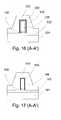
- FIGS. 18 a - 18 eshow the steps in the fabrication of the strained silicon finFET device in accordance with one embodiment of the invention, a silicon layer on a seed fin structure, with the seed fin structure generated from a underseed layer.
- a silicon on insulator substrate having a silicon-containing multilayer on an insulator layeris provided.
- the silicon-containing multilayercomprises a silicon germanium layer 204 on a silicon layer 203 .
- the silicon germanium layer 204is preferably epitaxially deposited on the silicon layer 203 , or can be germanium implanted into a silicon layer.
- a photoresistis applied to define a pattern through the use of optical lithography, electron beam lithography, x-ray lithography, or other conventional means to produce a photoresist mask comprising a fin channel between a source and drain structures.
- an etch processis used to pattern the silicon germanium layer 204 and the silicon layer 203 .
- the photoresistis stripped and the partially-fabricated device is shown in FIG. 18 b.
- the device formationincludes a source 207 and a drain 208 sandwiching a strained silicon germanium seed fin 206 on an underseed layer 205 .
- a sacrificial oxidation processmay be used to repair any damage done to the seed fin surface during the etch process.
- the oxidation processmay also be used to reduce the seed fin width, thereby allowing sub-lithographic dimension to be achieved.
- the sacrificial oxidationmay be performed by thermal oxidation process or rapid thermal oxidation process.
- the sacrificial oxideis then stripped to expose the silicon and silicon germanium surface.
- the height of the finis preferably between 10 nm to 200 nm, and the width of the fin is preferably between 5 nm to 100 nm.
- a selective epitaxial silicon layeris next deposited on the seed fin surface as shown in FIG. 18 c.
- the silicon thicknessis between 5 nm to 15 nm and is under stress due to the mismatched lattice with the silicon germanium seed fin 206 and the silicon underseed layer 205 .
- the epitaxial silicon layerforms the strained silicon channel 210 , and also covers the drain 211 and the source 212 .
- a channel ion implantation stepmay be applied to the silicon channel fin structure to optimize the device performance such as work function adjustments.
- the implanted dopantsmay be selected to permit dual work function adjustments for both p-type and n-type devices. Since the fin is thin, channel ion implantation doping may not be required to suppress short channel effect.
- the threshold voltage of the devicecan be controlled by adjusting the work function of the gate, for example by using silicon germanium alloy or a refractory metal or compound such as titanium nitride.
- a gate dielectric layer 213is grown or deposited on the strained silicon channel fin structure.
- the gate dielectriccan thermally grown silicon oxide, deposited silicon oxide, silicon nitride, a high dielectric constant material such as hafnium oxide, zirconium oxide, aluminum oxide, hafnium silicate, zirconium silicate, aluminum silicate, or any combination or alloy thereof.
- the oxide equivalent thickness of the gate dielectricis preferably between 0.3 nm and 10 nm, and more preferably between 0.3 nm and 3 nm.
- a gate material layeris deposited over the surface.
- the gate materialcan be polysilicon, silicon germanium, a refractory metal or compound such as titanium nitride or molybdenum, or other suitable conductive material such as aluminum, copper, or aluminum copper alloy. If the polysilicon gate material is used, the gate may be doped by ion implantation at this step.
- a gate maskis defined, preferably by photolithography technique, and then the underlying gate material is etched to form the gate electrode 216 and the gate 215 across the strained silicon channel 210 . The gate etching process stops on the gate dielectric 213 and the insulator layer 202 .
- the gate etchingcan stop on the hard mask instead on the thin gate dielectric, and therefore the hard mask can protect the silicon active area during the gate etching step.
- the gate 215is electrically isolated from the silicon channel 210 by the gate dielectric 213 .
- a light implant of appropriate dopantsthen may be used to form a lightly doped drain (LDD) and/or halo region.
- LDDlightly doped drain
- a spacerthen is formed on the sidewalls of the gate and the channel by deposition and non-isotropic etching of a dielectric such as silicon oxide or silicon nitride. The spacer on the sidewalls of the channel or other areas may be removed if desired by an additional etching, leaving the gate spacer 217 on either side of gate 215 as shown in FIG. 18 d.
- the polysilicon gate 225may also be doped at this step if not already doped.
- the dopingmay be accomplished by ion implantation, gas immersion laser doping, ion shower doping, gas or solid source diffusion.
- the dopant species and concentrationare chosen to achieve the required device characteristics such as n-type or p-type device.
- Angled or shallow ion implantationmay be used to dope the sides and top of the source and drain region. Any implant damage can be annealed at high temperatures.
- the series resistance of the source and draincan also be reduced by treating the source 221 and drain 220 with a highly conductive material such as a silicide deposition process (where a silicide is deposited on the source and drain) or a self aligned silicide (salicide) process (where a metal is deposited on the source and drain and subsequently reacts with silicon to form a silicide).
- a silicide deposition processwhere a silicide is deposited on the source and drain
- sialicideself aligned silicide
- a number of silicide or salicide processesare available such as titanium silicide, cobalt silicide, nickel suicide, or palladium silicide (FIG. 18 e ).
- the processingcan be continued with other state of the art device fabrication processes to finish the device or circuit fabrication.
- the methodcan use a bulk substrate or an insulator substrate (such as glass or plastic) instead of a SOI substrate.
- the methodcan also be used to fabricate vertically aligned NMOS and PMOS transistors separated by a dielectric layer and having a common gate, for example, see Hu et al., U.S. Pat. No. 6,413,802, hereby incorporated by reference.
- CMP techniquecan also be employed for the fabrication of the finFET structure according to the present invention, for example, see Muller et al., U.S. Pat. Nos. 6,252,284 and 6,432,829, hereby incorporated by reference.
- the methodcan also be used to fabricate strained silicon finFET device where the double gates are two separate gates with two separate gate electrodes, for example see Yu, U.S. Pat. No. 6,458,662, hereby incorporated by reference.
- the methodcan also be used to fabricate strained silicon finFET device where the double gates have different widths, for example see Ieong et al., U.S. Pat. No. 6,492,212, hereby incorporated by reference.
Landscapes
- Thin Film Transistor (AREA)
- Insulated Gate Type Field-Effect Transistor (AREA)
Abstract
Description
- This invention related generally to semiconductor devices including field effect transistors (FETs), metal-oxide-semiconductor FETs (MOSFETs), and more particularly related to improved semiconductor devices having double gates and strained channel.[0001]
- Field effect transistors (FETs) and particularly Metal-Oxide-Semiconductor field effect transistors (MOSFETs) are the dominant electronic devices in use today. The performance of these devices has been improved steadily through the reduction in device dimensions, from 10-20 μm channel length in the '70 to 100 nm channel length in '00 technology.[0002]
- As the channel length becomes smaller than 100 nm, MOSFET devices experience certain deleterious performance due to their size, such as the short channel effect caused by the close proximity of the source and drain, resulting in the reduction of the threshold voltage and the increase of sub-threshold current. With a short channel length, the source and drain regions may extend towards each other and may essentially occupy the entire channel area between the source and the drain. As a result of this effective occupation of the channel area by the source and drain, the channel is in part depleted and the gate charge necessary to alter the source and drain current flow is reduced. Thus the interaction between the source and drain of the MOSFET degrades the ability of the gate to control the operation of the device.[0003]
- Therefore, scaling of conventional bulk MOSFET devices beyond the 50 nm process generations is very difficult. Straightforward scaling requires ultra thin gate dielectric (equivalent oxide thickness should be less than 0.5 nm), ultra shallow junction (less than 10 nm depth for reducing short channel effect) and high concentration channel doping (>10[0004]18cm−3), all of which generate different problems of similar magnitude. For example, ultra thin gate oxide (less than 1-2 nm) has significant problem of tunneling current, and ultra shallow junction has significant problem of low sheet resistance and junction lateral steepness.
- Significant innovations have been made to the conventional bulk MOSFET devices to improve their performance. Silicon-On-Insulator (SOI) substrate has enabled MOSFET devices to have higher speed, lower power and higher density. Strain-induced band modification of the device channel has enabled MOSFET devices to have enhanced carrier mobility and therefore increased drive current. Double gate MOSFET structure allows gate control of the channel from both sides, reducing short channel effect and allowing more current flow.[0005]
- SOI wafers improve the transistor performance by reducing the operating silicon volume and by isolating the transistors. The thin surface silicon layer limits the volume of silicon that needs to be charged to switch the transistor on and off, and therefore reduces the parasitic capacitance of the transistor and increases the switching speed. The insulating layer isolates the transistor from its neighbors, and therefore reduces the leakage current and allows the transistor to operate at lower supply voltages and thus the transistors can be smaller and more densely packed.[0006]
- Further improvement of the MOSFET device performance is the introduction of strain-induced band modification of the device channel. Generally speaking, a compressive strained channel MOSFET has significant hole mobility enhancement, and a tensile strained channel MOSFET achieves both significant hole and electron mobility enhancement. Enhanced carrier mobility allows strained silicon MOSFET devices to exhibit vastly increased performance over their bulk silicon counterparts at identical gate lengths.[0007]
- Double gate MOSFET structure offers improvement for short channel effect reduction since it adds another gate on either side of the channel to allow gate control of the channel from both sides. Additionally, when the device is turned on using both gates, two conduction layers are formed, allowing more current flow. An extension of the double gate is the wrap-around gate where the gate is surrounding the channel. One variation of double gate MOSFET structure is finFET, a double gate device consists of a silicon channel formed in a silicon vertical fin controlled by a self-aligned double gate.[0008]
- The present invention discloses a novel strained silicon finFET device on an insulator substrate having the advantages of finFET structure for suppressing short channel effect and strained channel MOSFET structure for mobility enhancement.[0009]
- The disclosed strained silicon finFET device is a double gate finFET device having a strained silicon fin channel fabricated on an insulator substrate. The strained silicon fin channel is fabricated by forming a silicon-containing epitaxial layer on a silicon-containing seed fin having different lattice constant. By growing an epitaxial layer on a seed fin, the epitaxial layer will follow the single crystal nature of the seed fin, and by having different lattice constant, the epitaxial layer will experience lattice stress, which gives rise to a strained channel layer. If the lattice constant of the seed fin is larger than the lattice constant of the epitaxial layer, the epitaxial layer will try to extend itself to match the larger lattice constant, and therefore experience tensile stress and forming a tensile strained channel fin structure. If the lattice constant of the seed fin is smaller than the lattice constant of the epitaxial layer, the epitaxial layer will try squeeze itself into the smaller lattice constant, and therefore experience compressive stress and forming a compressive strained channel fin structure.[0010]
- In one embodiment of the invention, the strained silicon fin channel comprises an epitaxial silicon layer deposited on a relaxed silicon germanium seed fin. Other embodiments of the invention include an epitaxial silicon layer deposited on a strained silicon germanium seed fin wherein the strained silicon germanium seed fin is deposited on an underseed relaxed silicon layer, and a strained channel silicon fin fabricated on a relaxed silicon germanium seed layer.[0011]
- In a variation of the above embodiments, the strained silicon channel fin structure comprises an epitaxial carbon doped silicon (SiC) layer or an epitaxial carbon doped silicon germanium (SiGeC) layer deposited on a silicon germanium or a silicon seed fin.[0012]
- The present invention strained silicon channel fin structure can be employed to fabricate a strained silicon finFET device. The present invention strained silicon finFET device comprises a thin strained silicon-containing fin channel standing on an insulator layer, sandwiching between a source and a drain. A gate dielectric and double gates cover the sides of the fin to form the inversion layers on the sides of the channel. The channel fin is sufficiently thin so that the two gates control the entire channel film. The double gates on the channel fin can suppress the short channel effect and enhance drive current. The strained channel can provide enhanced carrier mobility to further improve the device performance. The present invention strained channel finFET device thus can improve hole carrier mobility and/or electron carrier mobility, in addition to suppressing short channel effect.[0013]
- FIG. 1 shows an embodiment of the present invention strained silicon channel fin structure.[0014]
- FIG. 2 shows a variation of the embodiment of FIG. 1.[0015]
- FIGS. 3[0016]a-3cshow the fabrication process of the embodiment of FIG. 1.
- FIGS. 4[0017]a-4cshow the fabrication process of the embodiment of FIG. 2.
- FIG. 5 shows another embodiment of the present invention strained silicon channel fin structure.[0018]
- FIG. 6 shows a variation of the embodiment of FIG. 5.[0019]
- FIGS. 7[0020]a-7cshow the fabrication process of the embodiment of FIG. 5.
- FIGS. 8[0021]a-8cshow the fabrication process of the embodiment of FIG. 6.
- FIG. 9 shows another embodiment of the present invention strained silicon channel fin structure.[0022]
- FIG. 10 shows a variation of the embodiment of FIG. 9.[0023]
- FIGS. 11[0024]a-11bshow the fabrication process of the embodiment of FIG. 9.
- FIGS. 12[0025]a-12bshow the fabrication process of the embodiment of FIG. 10.
- FIG. 13 shows a perspective view of the present invention strained silicon finFET device.[0026]
- FIG. 14 shows different views of an embodiment of the disclosed strained silicon finFET device.[0027]
- FIG. 15 shows a variation of the embodiment of FIG. 14.[0028]
- FIG. 16 shows another variation of the embodiment of FIG. 14.[0029]
- FIG. 17 shows another variation of the embodiment of FIG. 14.[0030]
- FIGS. 18[0031]a-18eshow the fabrication steps of the strained silicon finFET device in accordance with one embodiment of the invention.
- The present invention discloses a strained silicon fin structure and a strained silicon finFET device employing the disclosed strained silicon fin structure. The strained silicon fin structure is fabricated by forming a silicon-containing epitaxial layer on a silicon-containing seed fin having different lattice constant. The strained silicon finFET device comprises a strained silicon fin structure standing on an insulator layer, sandwiching between a source and a drain with a gate dielectric and a double gates covering the sides of the strained silicon fin structure to form the inversion layers on the sides of the fin.[0032]
- The present invention strained silicon fin structure comprises a seed fin structure disposed on an insulator substrate, and a strained channel layer fabricated on the seed fin structure. The channel layer material has a lattice constant different than the lattice constant of the seed fin material, and therefore the channel layer becomes a strained channel layer due the lattice mismatch between the seed fin and the channel layer.[0033]
- There are various variations of the present invention strained silicon fin structure: the seed fin can be strained, or relaxed (no strained at all or minimum strained); the channel layer can cover only the top side of the seed fin, or only the two sidewalls of the seed fin, or both the top side and the two sidewalls of the seed fin.[0034]
- An embodiment of the present invention strained silicon fin structure is shown in FIG. 1 wherein the channel layer covers both the top side and the two sidewalls of the seed fin. The seed fin of this embodiment can be a strained seed fin, but preferably a relaxed seed fin.[0035]
- In FIG. 1, a strained[0036]
channel silicon layer 11 covers a relaxed silicon germaniumfin seed fin 10 on aninsulator layer 12. The relaxedsilicon germanium fin 10 is preferably disposed on an insulator layer12 (such as silicon dioxide) on asilicon substrate 13. Theseed fin 10 is a relaxed silicon germanium fin having lattice constant larger than the lattice constant of silicon, therefore theepitaxial silicon layer 11 grown on theseed fin 10 will be tensilely strained. - The relaxed silicon germanium fin structure is preferably fabricated from a silicon germanium-on-insulator (SGOI) substrate with the concentration of germanium ranging from 10% to 100%. Then the SGOI substrate is patterned into a silicon germanium fin structure. Then a silicon layer is epitaxially deposited on the silicon germanium fin structure. The epitaxial deposition is preferably selectively epitaxial deposition wherein the deposition only occurs on the silicon germanium exposed surfaces. The silicon is under biaxial tensile stress because the lattice constant of silicon is smaller than the lattice constant of silicon germanium. The degree of tensile stress is a function of the concentration of germanium and can be optimized for the desired properties of the silicon device. The strained silicon fin structure as shown in FIG. 1 can become triple gate device in a finFET structure because the silicon channel covers two sides and top of the seed fin structure. The height H of the seed fin is preferably in the range of 10 nm to 200 nm, and the thickness T of the seed fin is preferably in the range of 5 nm to 100 nm. The epitaxial silicon layer thickness is preferably in the range of 5 to 15 nm. The optimized dimensions of the disclosed strained silicon fin structure are preferably chosen to ensure fully depleted body under the operation conditions of the finFET device.[0037]
- The patterning of the silicon germanium fin from the SGOI substrate is preferably by photolithography where a patterned mask is provided on the substrate, then the substrate is patterned according to the pattern mask, and then the patterned mask is removed. The patterned mask is preferably a photoresist layer, coated and exposed to UV light under a photo mask to transfer a pattern from the photo mask onto the photoresist. The photoresist mask protects the substrate during an etch step to transfer the pattern from the photoresist onto the substrate. And then the photoresist mask can be stripped. The pattern transfer etching is preferably accomplished by reactive ion etching or by wet etches.[0038]
- SGOI substrates belong to a class of Silicon-On-Insulator (SOI) substrates. The SOI substrate typically consists of a thin surface layer of single crystal silicon on an underlayer of insulating material on a bulk silicon wafer. The thin surface silicon layer, typically a few tens of nanometers to several microns thick, is the silicon channel of the transistor. The insulating layer, usually made of silicon dioxide, is referred to as the buried oxide and is usually a few hundreds of nanometers thick. The present invention is not limited to just silicon, but applicable to various silicon-containing materials or semiconductor materials such as silicon germanium, silicon carbon, or compound semiconductor materials. Therefore the term “silicon” in “strained silicon fin structure” and “strained silicon finFET device” can mean silicon germanium, carbon doped silicon, or other semiconductor material. The term SOI used in the present invention is also broadened to include all substrates having a thin semiconductor layer on an insulator on a semiconductor substrate. Examples include a silicon layer on a silicon dioxide insulating layer on a silicon substrate (SOI), and a silicon germanium layer on a silicon dioxide insulating layer on a silicon substrate (SGOI). Other example is a carbon doped silicon layer on a silicon dioxide insulating layer on a silicon substrate. The insulator substrate used in the present invention means a substrate having a multilayer on an insulator on a semiconductor support layer. The multilayer can comprise 2 or more semiconductor layers having mismatched lattice constants so that the upper semiconductor layer can be under strain. The bottommost layer of the multilayer is generally a part of the wafer substrate, such as a silicon layer in a SOI substrate, or a silicon germanium layer in a SGOI substrate. To fabricate the insulator substrate having a multilayer, the upper layers of the multilayer can be epitaxially deposited on the bottommost layer of the SOI or SGOI wafer. The multilayer can also comprise a plurality of semiconductor layers and a hard mask layer. Also, the term SOI substrate in the present invention also covers all substrates having similar structures (semiconductor/insulator/semiconductor) such as SIMOX substrates.[0039]
- FIG. 2 shows a variation of the above strained silicon fin structure with the addition of a hard mask layer on the seed fin structure. In this variation, the channel layer cover only the two sidewalls of the seed fin structure. With a[0040]
hard mask 14 on the seed fin, theepitaxial silicon layer 11′ only deposited on the silicon germanium exposed sidewall surfaces, and not on the top of the seed fin. The strained silicon channel fin structure as shown in FIG. 2 can become double gate device in a finFET structure because the silicon channel covers only two sides of the seed fin structure. - The epitaxial[0041]
channel silicon layer germanium seed fin 10 will be tensilely strained because the lattice constant of silicon is smaller than that of silicon germanium. Due to this tensile strain, the six-fold degeneracy of the electron conduction band of the silicon layer is split into a two-fold degenerate band and a four-fold degenerate band. The two-fold degenerate band has smaller energy, and therefore the electrons have smaller effective mass in this band, resulting in the electrons moving faster in the strained silicon channel of the silicon germanium/silicon heterojunction. Thus the mobility of the electrons in the strained silicon channel increases, resulting in the increased speed of the operating transistor. In addition, since the energy level of the two-fold degenerate band is lower than the energy level at the edge of the conduction band in the silicon germanium layer, the silicon germanium/silicon heterojunction serves as a heterobarrier to confine the electrons in the silicon channel. - The tensile strain of the silicon layer also serves to split the two-fold degeneracy valence band into a light hole band and a heavy hole band. Similar to the case of the conduction band, the light hole band has smaller energy, resulting in smaller effective mass of the holes, and an increase in hole mobility in the strained silicon channel device.[0042]
- In another variation of the above embodiment, the channel layer is an epitaxial carbon doped silicon (SiC) layer or an epitaxial carbon doped silicon germanium (SiGeC) layer. Since the lattice constant of carbon is smaller than the lattice constant of silicon or germanium, carbon doped silicon layer or carbon doped silicon germanium layer fabricated on the silicon germanium seed fin will be tensilely strained, and thus forming a strained carbon doped silicon or a carbon doped silicon germanium fin structure. The concentration of carbon in the carbon doped silicon or silicon germanium is preferably less than 30%.[0043]
- Similar to strained silicon channel mobility enhancement, the degeneracy of the conduction and valence bands in the SiC and SiGeC layer is similarly split, resulting in an enhancement of electron and hole mobility of the strained SiC and SiGeC channel layer. A further advantage of strained SiC or SiGeC channel layer is that the energy level of the light hole band is higher, and thus the light holes can also be confined in the strained SiC or SiGeC channel layer, similar to and in addition to the confinement of the light electrons.[0044]
- A further advantage of the strained SiC or SiGeC channel layer is that the seed fin can be silicon. Thus a variation of the above embodiment comprises a SiC or SiGeC channel layer fabricated on a silicon seed fin. Because of the use of silicon wafer substrate, a relaxed silicon seed fin on a silicon-on-insulator (SOI) substrate can be achieved with lower defect level than a relaxed silicon germanium seed layer. For example, to achieve a relaxed silicon germanium layer, the silicon germanium layer should be grown on the silicon substrate until the silicon germanium becomes thick enough to reduce the lattice strain of the silicon germanium layer. However, when the lattice strain of the silicon germanium is relaxed, a large number of dislocations can be generated in the silicon germanium layer. These dislocations may deteriorate the performance characteristics of the transistor and its long-term reliability. Better technology is currently available to reduce the defect level in SGOI substrates, but in general, SOI substrates are more technologically advanced.[0045]
- In a further variation of the above embodiment, the seed layer is a silicon seed fin, and the epitaxial layer is an epitaxial silicon germanium layer. Because the lattice constant of silicon is smaller than the lattice constant of silicon germanium, the epitaxial silicon germanium layer fabricated on the silicon seed layer will have a compressive strain, and thus forming a compressive strained silicon germanium channel fin structure. In general, compressive strained channel finFET has enhanced hole mobility but little or no enhanced electron mobility, and thus has significant mobility improvement on p-channel transistors.[0046]
- The fabrication of the above disclosed strained silicon fin structure can be accomplished by semiconductor fabrication process technology as disclosed below. Although illustrated and described below with reference to certain specific fabrication processes, the present invention is nevertheless not intended to be limited to the details shown. The general process of semiconductor fabrication has been practiced for many years, and due to the multitude of different ways of fabricating a device or structure, various modifications may be made in the fabrication process details within the scope and range of the present invention and without departing from the meaning of the invention.[0047]
- The starting substrate of the above embodiment is a relaxed[0048]
silicon germanium layer 15 on aninsulator 12 on a silicon substrate13 (SiGe-On-Insulator, SGOI) (FIG. 3a). A fin structure is patterned on the SGOI substrate. The patterning of the silicon germanium fin is preferably by photolithography process. The silicongermanium fin structure 10 after the patterning process is shown in FIG. 3bwith a thickness T and height H. FIG. 3bshows the etching of thesilicon germanium layer 15 and stopping on theinsulator layer 12, but the pattern etching of the fin structure may be over-etched onto theinsulator layer 12. The fabrication process continues with a selective deposition of anepitaxial silicon layer 11, covering the exposed surface of the silicon germanium (FIG. 3c). Due to the mismatched lattice constants between the silicon germanium seed fin structure and the epitaxial deposited silicon layer, the deposited silicon layer is under strained to form a strained silicon fin structure. - In a variation of the above process sequence, a[0049]
hard mask 16 can be first deposited on thesilicon germanium layer 15 to form amultilayer 16/15 on aninsulator 12 on a silicon substrate13 (FIG. 4a). Then the fabrication process continues as above with the patterning of a fin structure comprising ahard mask section 14 on a silicon germanium fin section10 (FIG. 4b) with a thickness T and height H, and the selective epitaxial deposition of asilicon layer 11′ (FIG. 4c). Since the hard mask is preferably an insulator material such as silicon dioxide or silicon nitride, the selective deposition of the silicon layer only deposited on the two sides of the seed fin structure. The hard mask then can be etched away, or left alone to protect the fin structure during subsequent process steps. - If the hard mask is etched away after the patterning of the fin structure and before the selective deposition of the silicon layer, the complete fin structure after FIG. 4[0050]bwill be similar to the fin structure shown in FIG. 3c.
- The above process sequence description uses silicon germanium and silicon as the seed fin and the strained channel respectively, but the process sequence can also be applied to other material variations. For example,[0051]
layer 15 can be a silicon layer from a SOI substrate comprising asilicon layer 15 on aninsulator 12 on asilicon substrate 13. Thusseed fin 10 can be a silicon seed fin and thechannel layer - The present invention strained silicon channel fin structure can further comprise an underseed layer disposed between the seed fin structure and the insulator substrate. The lattice constant of the underseed layer is different from the lattice constant of the seed fin, therefore forcing the seed fin to be strained. In this embodiment, the channel layer can cover both the top side and the two sidewalls of the seed fin, or only the two sidewalls of the seed fin with the help of a hard mask.[0052]
- FIG. 5 shows the embodiment of the present invention strained silicon channel fin structure with the strained seed fin disposed on an underseed layer. The[0053]
strained channel silicon 21 covers the strained silicon germaniumfin seed layer 20 on a relaxedsilicon underseed layer 25 on aninsulator layer 22. The relaxedsilicon underseed layer 25 is preferably disposed on an insulator layer12 (such as silicon dioxide) on asilicon substrate 23. Starting from a silicon-on-insulator substrate having a multilayer on an insulator layer, the silicon-on-insulator substrate is patterned into a multilayer seed fin structure. The multilayer is silicon germanium on silicon, preferably fabricated by epitaxially deposition of a layer of silicon germanium on a SOI substrate. The multilayer comprises2 semiconductor layers (silicon germanium layer and silicon layer) having mismatched lattice constant to generate the strained in the upper silicon germanium layer. Then asilicon channel layer 21 is epitaxially deposited on the multilayer fin seed structure. The epitaxial deposition is preferably selectively epitaxial deposition wherein the deposition only occurs on the silicon germanium or silicon surface. The seed fin structure has a thickness of T and a height of H as shown in FIG. 5. - The[0054]
silicon underseed layer 25 has a relaxed silicon lattice dSibecause of the SOI substrate. The lattice constant for thesilicon underseed layer 25 is then xSi=ySi=zSi=dSi. For the silicongermanium seed layer 20 deposited on the silicon, the lattice constant in the substrate xy plane will preferably match the lattice constant of the silicon underseed layer, therefore the deposited SiGe lattice constant is smaller in the xy plane than the relaxed SiGe lattice constant dSiGe: xSiGe=xSi<dSiGe, and ySiGe=ysi<dSiGe. The lattice constant of the deposited silicon germanium in the z direction has no such constraint, and therefore trying to compensate for the compressive of the lattice constant in the xy direction by becoming tensile in that direction. Thus the deposited SiGe lattice constant could be larger in the z direction than the relaxed SiGe lattice constant dSiGe: zSiGe>dSiGe. The schematic of the lattice constant of silicon and silicon germanium layers are shown in the inset of FIG. 5. - The epitaxial silicon layer deposited on the strained silicon germanium seed layer will experience some strain. The silicon germanium might experience some lattice shrinkage in the z direction, but in general, the silicon germanium is rigid enough to prevent serious lattice shrinkage, and the lattice constant of the deposited silicon germanium in the z direction could still be larger than the relaxed silicon germanium lattice constant. The epitaxial deposited silicon layer will have the lattice constant x′[0055]Si, y′Siand z′Siin the x, y, and z directions respectively. The lattice constant of the epitaxial deposited silicon layer in the y and z directions will preferably follow the underlayer lattice constants, namely y′Si=ySi(the relaxed silicon lattice constant) in the y direction, and z′Si=zSiGe(the tensile strained silicon germanium lattice constant, larger than the relaxed silicon lattice constant) in the z direction. In the x direction, there is no such constraint, and the lattice constant of the epitaxial deposited silicon layer in the x direction x′Sican be smaller or larger than the relaxed silicon lattice constant dSi. The epitaxial silicon layer could be under tensile strained in the z direction due to the silicon germanium seed. This strain could modify the supposedly stress-free condition of the silicon layer in the y direction, and put the silicon layer in a tensile stress. Even with the silicon germanium lattice constant zSiGedecreasing due to the compressive strain by the epitaxial silicon layer, the epitaxial silicon layer and the silicon germanium will reach an equilibrium condition where both layers could be under strain. It is estimated that under this equilibrium condition, the silicon germanium layer could be under compressive strain in all directions and the epitaxial silicon layer could be under tensile stress in all directions. The compressive strain in the silicon germanium seed layer will further benefit the hole mobility in p-channel PMOS finFET device under this embodiment of the present invention. The silicon germanium layer is preferably having a concentration of germanium ranging from 10% to 100%, and more preferably from 10% to 50%.
- FIG. 6 shows a variation of the above strained silicon channel fin structure. If a[0056]
hard mask 24 was used and left on the seed fin before the selective epitaxial deposition of the silicon layer, thesilicon 21′ only deposited on thesilicon germanium 20 andsilicon 25 exposed surface, and not on the top of the seed fin. - In a variation of the above embodiment, the epitaxial layer is an epitaxial carbon doped silicon (SiC) layer or an epitaxial carbon doped silicon germanium (SiGeC) layer. Since the lattice constant of carbon is smaller than the lattice constant of silicon or germanium, carbon doped silicon layer or carbon doped silicon germanium layer fabricated on the silicon germanium seed layer will have a tensile strain, and thus forming a strained carbon doped silicon or a carbon doped silicon germanium fin structure.[0057]
- Fabrication process of the above embodiment can start on a[0058]
silicon layer 26 on aninsulator 22 on a silicon substrate23 (Si-On-Insulator, SOI wafer). The thickness of the silicon layer is preferably between 5 nm to 20 nm, therefore a thinning process can be applied if the silicon thickness of the starting SOI wafer is outside of this range. A preferred thinning process is to oxidize the silicon layer and then wet etch the silicon oxide layer. Then asilicon germanium layer 27 is deposited on the silicon layer26 (FIG. 7a). FIG. 7ais a silicon on insulator substrate in which a silicon-containing multilayer (in this case, a silicon germanium/silicon multilayer) is disposed on an insulator layer. Due to the mismatched lattices between silicon and silicon germanium, thesilicon germanium layer 27 is under lattice strained. A fin structure is then patterned on the silicon germanium/silicon substrate. The patterning of the silicon germanium/silicon fin is preferably by photolithography process. The fin structure consists of a silicongermanium seed fin 20 on asilicon underseed 25 is shown in FIG. 7b.The pattern etching of the fin structure may be over-etched onto theinsulator layer 22, or onto thesilicon substrate 23. The fabrication process continues with a selective deposition of anepitaxial silicon layer 21, covering the exposed surface of the silicon germanium and silicon (FIG. 7c). Due to the mismatched lattice constants between the strained silicon germanium seed fin structure and the epitaxial deposited silicon layer, the deposited silicon layer is under strained to form a strained silicon fin structure. - In a variation of the above process sequence, a[0059]
hard mask 28 can be deposited on the silicon germanium layer27 (FIG. 8a). FIG. 8ais a silicon on insulator substrate in which a silicon-containing multilayer (in this case, a hard mask/silicon germanium/silicon multilayer) is disposed on an insulator layer. Then the fabrication process continues as above with the patterning of a fin structure comprising ahard mask section 24 on a silicongermanium fin section 20 on a silicon underseed section25 (FIG. 8b), and the selective epitaxial deposition of asilicon layer 21′ (FIG. 8c). Since the hard mask is preferably an insulator material such as silicon dioxide or silicon nitride, the selective deposition of the silicon layer only deposited on the two sides of the seed fin structure. The hard mask then can be etched away, or left alone to protect the fin structure during subsequent process steps. - If the hard mask is etched away after the patterning of the fin structure and before the selective deposition of the silicon layer, the complete fin structure after FIG. 8[0060]bwill be similar to the fin structure shown in FIG. 7c.
- Another embodiment of the present invention strained silicon channel fin structure has the channel layer covering only the top side of the seed fin. The seed fin of this embodiment can be a strained seed fin, but preferably a relaxed seed fin.[0061]
- In FIG. 9 the[0062]
strained channel silicon 31 is fabricated on the relaxed silicongermanium seed layer 30 on aninsulator layer 22. The relaxed silicongermanium seed layer 30 is preferably disposed on an insulator layer32 (such as silicon dioxide) on asilicon substrate 33. FIG. 10 shows a variation of the above strained silicon channel fin structure comprising ahard mask 34 on thestrained silicon fin 31. - In a variation of the above embodiment, the strained channel material is carbon doped silicon (SiC) or carbon doped silicon germanium (SiGeC). In further variations of the above embodiment, the seed layer is a silicon layer of a SOI substrate. In these variations, the strained channel can be silicon germanium, carbon doped silicon (SiC) or carbon doped silicon germanium (SiGeC).[0063]
- The fabrication process of the above embodiment starts with a[0064]
silicon layer 36 on aninsulator 32 on a silicon substrate33 (Si-On-Insulator, SOI wafer). The thickness of the silicon layer is preferably between 5 nm to 20 nm, therefore a thinning process can be applied if the silicon thickness of the starting SOI wafer is outside of this range. Then asilicon germanium layer 37 is deposited on the silicon layer36 (FIG. 11a). A fin structure is then patterned on the silicon germanium/silicon substrate, stopping on theinsulator layer 32, or over-etched onto theinsulator layer 32 or thesilicon substrate 33. The patterning of the silicon germanium/silicon fin is preferably by photolithography process. The fin structure consisting of a silicon germanium strainedchannel fin 31 on asilicon seed 30 is shown in FIG. 11b. - In a variation of the above process sequence, a[0065]
hard mask 38 can be deposited on the silicon germanium layer37 (FIG. 12a). Then the fabrication process continues as above with the patterning of a fin structure comprising ahard mask section 34 on a silicongermanium fin section 31 on a silicon seed section30 (FIG. 12b). - The present invention discloses a strained silicon fin structure. Within the scope of the invention, the basic component of the strained silicon fin structure is silicon, therefore the term “strained silicon” within the scope of the invention refers to “strained silicon-containing” material, such as silicon germanium, carbon doped silicon. Although the above description details silicon-containing fin structure, the present invention also could be used for compound semiconductors, or other semiconductor materials wherein the strained semiconductor channel fin structure could make an improvement in carrier mobility. Furthermore, although the above description details a strained silicon fin structure on an insulator substrate, the present invention could also be used for bulk semiconductor substrate such as a silicon wafer.[0066]
- The present invention strained silicon channel fin structure is also employed to fabricate a strained silicon finFET device as disclosed below.[0067]
- The present invention finFET device is a double gate MOSFET device consisting of a strained silicon channel formed in a silicon vertical fin controlled by a self-aligned double gate. The finFET structure includes an ultra thin silicon fin for suppression of the short channel effect, and two self-aligned gates to control the entire fully depleted channel film. In finFET structure, the gate length of the finFET structure is the distance between the source and drain and often is defined by a spacer gap. The device width of the finFET structure is the fin height because the current flows along the vertical surface of the fin. This width definition counts only one side of the channel. Because there are two gates controlling both sides of the fin, the fin thickness equals the twice the body thickness. The channel film width in a finFET device is less than channel length, and the double gates on the channel fin effectively suppress short channel effect and enhance drive current. Self-aligned gates in which the two gates are self-aligned to each other and to the source and drain regions are preferred for reducing parasitic gate capacitance, series resistance and for control of the channel length. The disclosed strained silicon finFET device can further have raised source and drain to reduce parasitic resistance. Since the fin is thin, doping of the fin is not required to suppress short channel effect and undoped silicon can be used as device channel, reducing mobility degradation due to impurity scattering.[0068]
- Further improvement of the present invention finFET device is the addition of the strained channel fin structure as disclosed above. A strained channel finFET device could achieves significant hole and/or electron mobility enhancement. Enhanced carrier mobility could allow strained silicon finFET devices to exhibit significantly increased performance over their bulk silicon counterparts or their non-strained silicon finFET counterparts at identical gate lengths.[0069]
- FIG. 13 shows a perspective view of the present invention strained silicon finFET device. The strained silicon finFET structure includes a strained[0070]
silicon fin structure 52 on aninsulator layer 42 on asubstrate 43, a gate dielectric layer covering the strained channel fin, and agate 48 extending across thestrain channel fin 52 and electrically isolated from thestrained channel fin 52 by the gate dielectric. The strained silicon finFET structure further includes asource 47 and adrain 51 sandwiching thestrained silicon fin 52. An optional dielectrichard mask 46 covers the source, drain and channel fin. Adielectric spacer 49 covers and isolates thegate 48. - The strained silicon finFET structure is preferably fabricated on an insulator substrate such as a silicon-on-insulator (SOI) substrate. It is also possible that the disclosed strained silicon finFET device is fabricated on a bulk semiconductor substrate such as a bulk silicon wafer.[0071]
- The disclosed strained silicon finFET device employs a strained silicon channel fin structure as disclosed in details above. To recapitulate, the disclosed strained silicon channel fin structure comprises a strained silicon-containing channel layer deposited on a seed fin having mismatched lattice. The mismatch lattices between the seed fin and the overlaid channel layer generates the strain in the channel layer.[0072]
- Various embodiments of the seed fin and the overlaid channel layer having mismatch lattices are:[0073]
- an epitaxial channel layer deposited on a seed fin, for example[0074]
- an epitaxial silicon layer deposited on a relaxed silicon germanium seed fin with the silicon germanium fin fabricated from a SGOI substrate;[0075]
- an epitaxial silicon germanium layer deposited on a relaxed silicon seed fin with the silicon fin fabricated from a SOI substrate;[0076]
- an epitaxial carbon doped silicon layer deposited on a relaxed silicon germanium seed fin with the silicon germanium fin fabricated from a SGOI substrate;[0077]
- an epitaxial carbon doped silicon layer deposited on a relaxed silicon seed fin with the silicon fin fabricated from a SOI substrate;[0078]
- an epitaxial carbon doped silicon germanium layer deposited on a relaxed silicon germanium seed fin with the silicon germanium fin fabricated from a SGOI substrate;[0079]
- an epitaxial carbon doped silicon germanium layer deposited on a relaxed silicon seed fin with the silicon fin fabricated from a SOI substrate;[0080]
- an epitaxial channel layer deposited on a seed fin with the seed fin fabricated on an underseed layer, for example[0081]
- an epitaxial silicon layer deposited on a silicon germanium seed fin on a silicon underseed layer with the multilayer silicon germanium/silicon fin fabricated from a SOI substrate;[0082]
- an epitaxial carbon doped silicon layer deposited on a silicon germanium seed fin on a silicon underseed layer with the multilayer silicon germanium/silicon fin fabricated from a SOI substrate;[0083]
- an epitaxial carbon doped silicon germanium layer deposited on a silicon germanium seed fin on a silicon underseed layer with the multilayer silicon germanium/silicon fin fabricated from a SOI substrate;[0084]
- a channel/seed multilayer on a insulator substrate fabricated into a fin structure, for example[0085]
- an epitaxial silicon layer deposited on a silicon germanium seed layer of a SGOI substrate;[0086]
- an epitaxial carbon doped silicon layer deposited on a silicon germanium seed layer of a SGOI substrate;[0087]
- an epitaxial carbon doped silicon germanium layer deposited on a silicon germanium seed layer of a SGOI substrate;[0088]
- an epitaxial carbon doped silicon layer deposited on a silicon seed layer of a SOI substrate;[0089]
- an epitaxial carbon doped silicon germanium layer deposited on a silicon seed layer of a SOI substrate.[0090]
- FIG. 14 shows the top view of the disclosed strained silicon finFET device having the first embodiment of a silicon layer on a seed fin structure without a hard mask. The finFET is a field effect transistor having a[0091]
source 106 and adrain 107 separated by achannel 104. Thechannel 104 conduction is controlled by thedouble gate 103, extending and covering thechannel 104, and connected to thegate electrode 108. Thedouble gate 103 is electrically isolated from thechannel 104 by aspacer 109 and agate dielectric 110. Thedouble gate 103 is actually a triple gate because it covers both sides and the top of thestrained silicon channel 104. The term “double gate” in the context of the present invention is a generic term to mean “more than one gate”, and therefore covers double or triple gate device. - FIG. 14 also shows the cross section AA′, cutting through the[0092]
fin channel 104 of the finFET structure. The finFET device is preferably fabricated on aninsulator layer 102 on asubstrate 101. The finFET channel is a strained silicon channel, comprising aseed fin 105 and astrained silicon channel 104, covering both sides and the top of theseed fin 105. The finFET device becomes a triple gate device because thegate 103 covers thestrained silicon channel 104 on both sides and also on the top of the fin. Thetriple gate 103 is isolated from thechannel 104 by agate dielectric 110. - FIG. 14 further shows the cross section BB′, cutting through the[0093]
triple gate 103 of the finFET structure. The cross section BB′ cuts through theseed fin layer 105 on ainsulator layer 102 and asubstrate 101, thestrained silicon channel 104 and thegate dielectric 110. Thetriple gate 103 also covers the top section of the fin structure, with thespacer 109 to isolate thetriple gate 103 from thesilicon channel 104. - In a variation of the above embodiment with a silicon layer on a seed fin with a hard mask, FIG. 15 shows the cross section AA′, cutting through the[0094]
fin channel 104 of the new variation finFET structure. The finFET channel is a strained silicon channel, comprising aseed fin 105, ahard mask 111 and astrained silicon channel 104 selectively grown on theseed fin 105. Thedouble gate 103 covers thestrained silicon channel 104 and is isolated from thechannel 104 by agate dielectric 110. - FIG. 15 also shows the cross section BB′ of the new variation finFET structure, cutting through the[0095]
double gate 103 of the finFET structure. The cross section BB′ cuts through theseed fin layer 105 positioned on ainsulator layer 102 and asubstrate 101, and thehard mask layer 111. Thedouble gate 103 has thespacer 109 to isolate thedouble gate 103 from thesilicon channel 104. - FIG. 16 shows the cross section AA′ for another embodiment of the finFET structure having a silicon layer on a seed fin structure with the seed fin structure generated from a underseed layer. The finFET device is fabricated on an[0096]
insulator layer 122 on asubstrate 121. The finFET channel is a strained silicon channel, comprising aseed fin 125 grown on anunderseed layer 132, and astrained silicon channel 124 selectively grown on theseed fin 125 and theunderseed layer 132. Thedouble gate 123 covers thestrained silicon channel 124 and is isolated from thechannel 124 by agate dielectric 130. - FIG. 17 shows the cross section AA′ for another embodiment of the finFET structure having a silicon layer on a seed layer. The finFET device is fabricated on an[0097]
insulator layer 142 on asubstrate 141. The finFET channel is a strained silicon channel, comprising aseed layer 145, and astrained silicon channel 144 grown on theseed layer 145. Thedouble gate 143 covers thestrained silicon channel 144 and is isolated from thechannel 144 by agate dielectric 150. - The disclosed strained silicon finFET structure is preferably having the thickness of the fin structure is between 10 nm to 200 nm, the width of the fin structure is between 5 nm to 100 nm, and the thickness of the strained channel is between 5 nm to 15 nm. The width of the present invention strained channel fin structure is preferably less than the gate length to ensure fully depleted body. The strained silicon finFET structure preferably has the strained channel fabricated on two sides of the fin structure, or more preferably on two sides and on top of the fin structure. The strained silicon finFET structure preferably further comprises LDD (lightly doped drain) and Halo implantation where the source and drain regions include a lightly doped region extending to the channel region, doping implantation for the strained channel, source and drain where the source and drain regions are preferably more heavily doped than the channel region, and the silicidation of the source, drain, and gates. The gate dielectric of the disclosed strained silicon finFET structure is preferably thermally grown silicon dioxide, deposited silicon dioxide, or high k dielectric material such as hafnium oxide, zirconium oxide, aluminum oxide, hafnium silicate, zirconium silicate, aluminum silicate, or any combination or alloy thereof. The equivalent silicon dioxide thickness of the gate dielectric is preferably between 0.3 nm and 3 nm. The gate of the disclosed strained silicon finFET structure is preferably polysilicon, doped polysilicon or metal.[0098]
- The fabrication of the above disclosed strained silicon finFET device can be accomplished by semiconductor fabrication process technology as disclosed below. Although illustrated and described below with reference to certain specific fabrication processes, the present invention is nevertheless not intended to be limited to the details shown. The general process of semiconductor fabrication has been practiced for many years, and due to the multitude of different ways of fabricating a device or structure, various modifications may be made in the fabrication process details within the scope and range of the present invention and without departing from the meaning of the invention.[0099]
- The fabrication process of the present invention strained silicon finFET device starts with the fabrication of a strained silicon channel fin structure as shown in FIG. 1, FIG. 2, FIG. 5, FIG. 6, FIG. 9, or FIG. 10. The fabrication process for these various embodiments are similar, and therefore only one embodiment is shown below.[0100]
- FIGS. 18[0101]a-18eshow the steps in the fabrication of the strained silicon finFET device in accordance with one embodiment of the invention, a silicon layer on a seed fin structure, with the seed fin structure generated from a underseed layer. In FIG. 18a,a silicon on insulator substrate having a silicon-containing multilayer on an insulator layer is provided. The silicon-containing multilayer comprises a
silicon germanium layer 204 on asilicon layer 203. Thesilicon germanium layer 204 is preferably epitaxially deposited on thesilicon layer 203, or can be germanium implanted into a silicon layer. Thesilicon layer 203 is a part of an insulator SOI or SIMOX substrate comprising asilicon substrate 201, a buriedoxide layer 202, and thesilicon layer 203. In other aspect of the invention, the multilayer can further comprise a hard mask layer deposited on top of the silicon germanium layer. Thesilicon layer 203 serves as an underseed layer with the thickness preferably between 5 nm to 20 nm. A silicon thinning step may be performed if the thickness of the silicon layer of the starting substrate is outside this range. The silicon thinning step is preferably an oxidation/etching step wherein the silicon is oxidized and then the silicon oxide is selectively etched away. The oxidation is preferably thermal oxidation or rapid thermal oxidation, and the selective etch is preferably wet etch with HF solution, or reactive ion etching. After thinning the silicon layer to the desired thickness, a layer ofsilicon germanium 204 is epitaxially deposited on thesilicon layer 203. The combined thickness of thesilicon germanium layer 204 and thesilicon layer 203 defines the width of the finFET device. The silicon germanium is under strained and will serves as a seed layer for the strained channel of the strained silicon finFET structure. A hard mask layer may be deposited (not shown) on the silicon germanium layer to protect the silicon germanium surface and to allow the use of aggressive etch chemistries such as plasma etching. - A photoresist is applied to define a pattern through the use of optical lithography, electron beam lithography, x-ray lithography, or other conventional means to produce a photoresist mask comprising a fin channel between a source and drain structures. After the photoresist mask definition, an etch process is used to pattern the[0102]
silicon germanium layer 204 and thesilicon layer 203. Then the photoresist is stripped and the partially-fabricated device is shown in FIG. 18b.The device formation includes asource 207 and adrain 208 sandwiching a strained silicongermanium seed fin 206 on anunderseed layer 205. A sacrificial oxidation process may be used to repair any damage done to the seed fin surface during the etch process. The oxidation process may also be used to reduce the seed fin width, thereby allowing sub-lithographic dimension to be achieved. The sacrificial oxidation may be performed by thermal oxidation process or rapid thermal oxidation process. The sacrificial oxide is then stripped to expose the silicon and silicon germanium surface. The height of the fin is preferably between 10 nm to 200 nm, and the width of the fin is preferably between 5 nm to 100 nm. - A selective epitaxial silicon layer is next deposited on the seed fin surface as shown in FIG. 18[0103]c.The silicon thickness is between 5 nm to 15 nm and is under stress due to the mismatched lattice with the silicon
germanium seed fin 206 and thesilicon underseed layer 205. The epitaxial silicon layer forms thestrained silicon channel 210, and also covers thedrain 211 and thesource 212. A channel ion implantation step may be applied to the silicon channel fin structure to optimize the device performance such as work function adjustments. The implanted dopants may be selected to permit dual work function adjustments for both p-type and n-type devices. Since the fin is thin, channel ion implantation doping may not be required to suppress short channel effect. The threshold voltage of the device can be controlled by adjusting the work function of the gate, for example by using silicon germanium alloy or a refractory metal or compound such as titanium nitride. - A[0104]
gate dielectric layer 213 is grown or deposited on the strained silicon channel fin structure. The gate dielectric can thermally grown silicon oxide, deposited silicon oxide, silicon nitride, a high dielectric constant material such as hafnium oxide, zirconium oxide, aluminum oxide, hafnium silicate, zirconium silicate, aluminum silicate, or any combination or alloy thereof. The oxide equivalent thickness of the gate dielectric is preferably between 0.3 nm and 10 nm, and more preferably between 0.3 nm and 3 nm. Next a gate material layer is deposited over the surface. The gate material can be polysilicon, silicon germanium, a refractory metal or compound such as titanium nitride or molybdenum, or other suitable conductive material such as aluminum, copper, or aluminum copper alloy. If the polysilicon gate material is used, the gate may be doped by ion implantation at this step. A gate mask is defined, preferably by photolithography technique, and then the underlying gate material is etched to form thegate electrode 216 and thegate 215 across thestrained silicon channel 210. The gate etching process stops on thegate dielectric 213 and theinsulator layer 202. If a hard mask is used, the gate etching can stop on the hard mask instead on the thin gate dielectric, and therefore the hard mask can protect the silicon active area during the gate etching step. Thegate 215 is electrically isolated from thesilicon channel 210 by thegate dielectric 213. A light implant of appropriate dopants then may be used to form a lightly doped drain (LDD) and/or halo region. A spacer then is formed on the sidewalls of the gate and the channel by deposition and non-isotropic etching of a dielectric such as silicon oxide or silicon nitride. The spacer on the sidewalls of the channel or other areas may be removed if desired by an additional etching, leaving thegate spacer 217 on either side ofgate 215 as shown in FIG. 18d. - After spacer formation is the formation of the source and drain by ion implantation. The[0105]
polysilicon gate 225 may also be doped at this step if not already doped. The doping may be accomplished by ion implantation, gas immersion laser doping, ion shower doping, gas or solid source diffusion. The dopant species and concentration are chosen to achieve the required device characteristics such as n-type or p-type device. Angled or shallow ion implantation may be used to dope the sides and top of the source and drain region. Any implant damage can be annealed at high temperatures. The series resistance of the source and drain can also be reduced by treating thesource 221 and drain220 with a highly conductive material such as a silicide deposition process (where a silicide is deposited on the source and drain) or a self aligned silicide (salicide) process (where a metal is deposited on the source and drain and subsequently reacts with silicon to form a silicide). A number of silicide or salicide processes are available such as titanium silicide, cobalt silicide, nickel suicide, or palladium silicide (FIG. 18e). The processing can be continued with other state of the art device fabrication processes to finish the device or circuit fabrication. - In an alternative embodiment, the method can use a bulk substrate or an insulator substrate (such as glass or plastic) instead of a SOI substrate. The method can also be used to fabricate vertically aligned NMOS and PMOS transistors separated by a dielectric layer and having a common gate, for example, see Hu et al., U.S. Pat. No. 6,413,802, hereby incorporated by reference. CMP technique can also be employed for the fabrication of the finFET structure according to the present invention, for example, see Muller et al., U.S. Pat. Nos. 6,252,284 and 6,432,829, hereby incorporated by reference. The method can also be used to fabricate strained silicon finFET device where the double gates are two separate gates with two separate gate electrodes, for example see Yu, U.S. Pat. No. 6,458,662, hereby incorporated by reference. The method can also be used to fabricate strained silicon finFET device where the double gates have different widths, for example see Ieong et al., U.S. Pat. No. 6,492,212, hereby incorporated by reference.[0106]
Claims (30)
Priority Applications (3)
| Application Number | Priority Date | Filing Date | Title |
|---|---|---|---|
| US10/602,436US7045401B2 (en) | 2003-06-23 | 2003-06-23 | Strained silicon finFET device |
| JP2004153999AJP2005019970A (en) | 2003-06-23 | 2004-05-24 | Strained silicon fin FET device |
| US11/327,092US7115945B2 (en) | 2003-06-23 | 2006-01-06 | Strained silicon fin structure |
Applications Claiming Priority (1)
| Application Number | Priority Date | Filing Date | Title |
|---|---|---|---|
| US10/602,436US7045401B2 (en) | 2003-06-23 | 2003-06-23 | Strained silicon finFET device |
Related Child Applications (1)
| Application Number | Title | Priority Date | Filing Date |
|---|---|---|---|
| US11/327,092DivisionUS7115945B2 (en) | 2003-06-23 | 2006-01-06 | Strained silicon fin structure |
Publications (2)
| Publication Number | Publication Date |
|---|---|
| US20040256647A1true US20040256647A1 (en) | 2004-12-23 |
| US7045401B2 US7045401B2 (en) | 2006-05-16 |
Family
ID=33518092
Family Applications (2)
| Application Number | Title | Priority Date | Filing Date |
|---|---|---|---|
| US10/602,436Expired - LifetimeUS7045401B2 (en) | 2003-06-23 | 2003-06-23 | Strained silicon finFET device |
| US11/327,092Expired - LifetimeUS7115945B2 (en) | 2003-06-23 | 2006-01-06 | Strained silicon fin structure |
Family Applications After (1)
| Application Number | Title | Priority Date | Filing Date |
|---|---|---|---|
| US11/327,092Expired - LifetimeUS7115945B2 (en) | 2003-06-23 | 2006-01-06 | Strained silicon fin structure |
Country Status (2)
| Country | Link |
|---|---|
| US (2) | US7045401B2 (en) |
| JP (1) | JP2005019970A (en) |
Cited By (120)
| Publication number | Priority date | Publication date | Assignee | Title |
|---|---|---|---|---|
| US20040147079A1 (en)* | 2002-06-10 | 2004-07-29 | Leonard Forbes | Output prediction logic circuits with ultra-thin vertical transistors and methods of formation |
| US20050035391A1 (en)* | 2003-08-14 | 2005-02-17 | Lee Deok Hyung | Multi-structured Si-fin and method of manufacture |
| US20050051825A1 (en)* | 2003-09-09 | 2005-03-10 | Makoto Fujiwara | Semiconductor device and manufacturing method thereof |
| US20050051812A1 (en)* | 2003-07-18 | 2005-03-10 | Interuniversitair Microelektronica Centrum (Imec Vzw) | Multiple gate semiconductor device and method for forming same |
| US20050148137A1 (en)* | 2003-12-30 | 2005-07-07 | Brask Justin K. | Nonplanar transistors with metal gate electrodes |
| US20050202608A1 (en)* | 2004-03-15 | 2005-09-15 | International Business Machines Corporation | Locally thinned fins |
| US20050199949A1 (en)* | 2002-08-23 | 2005-09-15 | Chau Robert S. | Tri-gate devices and methods of fabrication |
| US20050218438A1 (en)* | 2004-03-31 | 2005-10-06 | Nick Lindert | Bulk non-planar transistor having strained enhanced mobility and methods of fabrication |
| US20050263795A1 (en)* | 2004-05-25 | 2005-12-01 | Jeong-Dong Choi | Semiconductor device having a channel layer and method of manufacturing the same |
| US6972461B1 (en)* | 2004-06-30 | 2005-12-06 | International Business Machines Corporation | Channel MOSFET with strained silicon channel on strained SiGe |
| US20060001109A1 (en)* | 2004-06-30 | 2006-01-05 | Shaheen Mohamad A | High mobility tri-gate devices and methods of fabrication |
| US20060022262A1 (en)* | 2004-07-30 | 2006-02-02 | Jae-Man Yoon | Semiconductor device having a fin structure and method of manufacturing the same |
| US20060063332A1 (en)* | 2004-09-23 | 2006-03-23 | Brian Doyle | U-gate transistors and methods of fabrication |
| US20060071275A1 (en)* | 2004-09-30 | 2006-04-06 | Brask Justin K | Nonplanar transistors with metal gate electrodes |
| US20060076625A1 (en)* | 2004-09-25 | 2006-04-13 | Lee Sung-Young | Field effect transistors having a strained silicon channel and methods of fabricating same |
| US20060131606A1 (en)* | 2004-12-18 | 2006-06-22 | Amberwave Systems Corporation | Lattice-mismatched semiconductor structures employing seed layers and related fabrication methods |
| US7074623B2 (en)* | 2002-06-07 | 2006-07-11 | Amberwave Systems Corporation | Methods of forming strained-semiconductor-on-insulator finFET device structures |
| US20060157794A1 (en)* | 2005-01-18 | 2006-07-20 | Doyle Brian S | Non-planar MOS structure with a strained channel region |
| US20060177998A1 (en)* | 2003-09-03 | 2006-08-10 | Harrity & Snyder, L.L.P. | Fully silicided gate structure for finfet devices |
| US20060240621A1 (en)* | 2005-04-21 | 2006-10-26 | Samsung Electronics Co., Ltd. | Double gate transistors having at least two polysilicon patterns on a thin body used as active region and methods of forming the same |
| US20070001198A1 (en)* | 2004-08-11 | 2007-01-04 | Hynix Semiconductor Inc. | Semiconductor device and method for forming the same |
| US20070001219A1 (en)* | 2005-06-30 | 2007-01-04 | Marko Radosavljevic | Block contact architectures for nanoscale channel transistors |
| US20070020936A1 (en)* | 2005-07-19 | 2007-01-25 | Micron Technology, Inc. | Methods of etching features into substrates |
| US20070040223A1 (en)* | 2005-08-17 | 2007-02-22 | Intel Corporation | Lateral undercut of metal gate in SOI device |
| US20070048947A1 (en)* | 2003-08-14 | 2007-03-01 | Lee Deok H | Multi-structured Si-fin and method of manufacture |
| US20070052041A1 (en)* | 2003-05-30 | 2007-03-08 | Haruyuki Sorada | Semiconductor device and method of fabricating the same |
| US20070087510A1 (en)* | 2005-10-12 | 2007-04-19 | Myung Jin Jung | Semiconductor devices and manufacturing methods of the same |
| US20070090416A1 (en)* | 2005-09-28 | 2007-04-26 | Doyle Brian S | CMOS devices with a single work function gate electrode and method of fabrication |
| US20070108536A1 (en)* | 2005-11-15 | 2007-05-17 | International Business Machines Corporation | QUASI SELF-ALIGNED SOURCE/DRAIN FinFET PROCESS |
| US20070120154A1 (en)* | 2005-11-30 | 2007-05-31 | International Business Machines Corporation | Finfet structure with multiply stressed gate electrode |
| US7241653B2 (en) | 2003-06-27 | 2007-07-10 | Intel Corporation | Nonplanar device with stress incorporation layer and method of fabrication |
| WO2007076791A1 (en)* | 2005-12-12 | 2007-07-12 | Infineon Technologies Ag | Method for the production of a compound semiconductor field effect transistor comprising a fin structure, and compound semiconductor field effect transistor comprising a fin structure |
| US7268058B2 (en) | 2004-01-16 | 2007-09-11 | Intel Corporation | Tri-gate transistors and methods to fabricate same |
| US20070221956A1 (en)* | 2006-03-23 | 2007-09-27 | Kabushiki Kaisha Toshiba | Semiconductor device and method of fabricating the same |
| US20070235818A1 (en)* | 2006-03-28 | 2007-10-11 | Anderson Brent A | Dual-plane complementary metal oxide semiconductor |
| US7348284B2 (en) | 2004-08-10 | 2008-03-25 | Intel Corporation | Non-planar pMOS structure with a strained channel region and an integrated strained CMOS flow |
| US20080099839A1 (en)* | 2006-06-14 | 2008-05-01 | Willy Rachmady | Ultra-thin oxide bonding for S1 to S1 dual orientation bonding |
| US7393733B2 (en)* | 2004-12-01 | 2008-07-01 | Amberwave Systems Corporation | Methods of forming hybrid fin field-effect transistor structures |
| US7396711B2 (en) | 2005-12-27 | 2008-07-08 | Intel Corporation | Method of fabricating a multi-cornered film |
| US20080176363A1 (en)* | 2005-07-27 | 2008-07-24 | Anderson Brent A | Virtual body-contacted trigate |
| US20080237675A1 (en)* | 2007-03-29 | 2008-10-02 | Doyle Brian S | Capacitor, method of increasing a capacitance area of same, and system containing same |
| US7449373B2 (en) | 2006-03-31 | 2008-11-11 | Intel Corporation | Method of ion implanting for tri-gate devices |
| US7456476B2 (en) | 2003-06-27 | 2008-11-25 | Intel Corporation | Nonplanar semiconductor device with partially or fully wrapped around gate electrode and methods of fabrication |
| US20080311732A1 (en)* | 2003-12-04 | 2008-12-18 | International Business Machines Corporation | Method for Forming Non-Amorphous, Ultra-Thin Semiconductor Devices Using Sacrificial Implantation Layer |
| US7479421B2 (en) | 2005-09-28 | 2009-01-20 | Intel Corporation | Process for integrating planar and non-planar CMOS transistors on a bulk substrate and article made thereby |
| US20090085114A1 (en)* | 2007-09-28 | 2009-04-02 | Muhammad Nawaz | Semiconductor Structure |
| US7518196B2 (en) | 2005-02-23 | 2009-04-14 | Intel Corporation | Field effect transistor with narrow bandgap source and drain regions and method of fabrication |
| WO2009070252A1 (en)* | 2007-11-30 | 2009-06-04 | Advanced Micro Devices, Inc. | A hetero-structured, inverted-t field effect transistor |
| US7547637B2 (en) | 2005-06-21 | 2009-06-16 | Intel Corporation | Methods for patterning a semiconductor film |
| US7550333B2 (en) | 2004-10-25 | 2009-06-23 | Intel Corporation | Nonplanar device with thinned lower body portion and method of fabrication |
| US7579280B2 (en) | 2004-06-01 | 2009-08-25 | Intel Corporation | Method of patterning a film |
| US20090315114A1 (en)* | 2008-06-23 | 2009-12-24 | Intel Corporation | Stress in trigate devices using complimentary gate fill materials |
| US20090321828A1 (en)* | 2008-06-26 | 2009-12-31 | International Business Machines Corporation | Structures, fabrication methods, design structures for strained fin field effect transistors (finfets) |
| US7772048B2 (en)* | 2007-02-23 | 2010-08-10 | Freescale Semiconductor, Inc. | Forming semiconductor fins using a sacrificial fin |
| US20100252816A1 (en)* | 2009-04-01 | 2010-10-07 | Taiwan Semiconductor Manufacturing Company, Ltd. | High-Mobility Multiple-Gate Transistor with Improved On-to-Off Current Ratio |
| US20100264470A1 (en)* | 2009-04-21 | 2010-10-21 | Applied Materials, Inc. | Nmos transistor devices and methods for fabricating same |
| US20100301392A1 (en)* | 2009-06-01 | 2010-12-02 | Chih-Hsin Ko | Source/Drain Re-Growth for Manufacturing III-V Based Transistors |
| CN101924105A (en)* | 2009-05-29 | 2010-12-22 | 台湾积体电路制造股份有限公司 | Integrated circuit structure |
| US20100320508A1 (en)* | 2007-09-12 | 2010-12-23 | Arizona Board Of Regents For And On Behalf Of Arizona State University | Horizontally depleted metal semiconductor field effect transistor |
| US7858481B2 (en) | 2005-06-15 | 2010-12-28 | Intel Corporation | Method for fabricating transistor with thinned channel |
| US7859053B2 (en) | 2004-09-29 | 2010-12-28 | Intel Corporation | Independently accessed double-gate and tri-gate transistors in same process flow |
| US7879675B2 (en) | 2005-03-14 | 2011-02-01 | Intel Corporation | Field effect transistor with metal source/drain regions |
| US20110073951A1 (en)* | 2009-09-30 | 2011-03-31 | International Business Machines Corporation | Enhanced stress-retention fin-fet devices and methods of fabricating enhanced stress retention fin-fet devices |
| US20110127580A1 (en)* | 2008-04-30 | 2011-06-02 | Industry-University Cooperation Foundation Hanyang University | Capacitor-less memory device |
| US20110175140A1 (en)* | 2009-12-17 | 2011-07-21 | Applied Materials, Inc. | Methods for forming nmos epi layers |
| US7989280B2 (en) | 2005-11-30 | 2011-08-02 | Intel Corporation | Dielectric interface for group III-V semiconductor device |
| US20110210393A1 (en)* | 2010-03-01 | 2011-09-01 | Taiwan Semiconductor Manufacturing Co., Ltd. | Dual epitaxial process for a finfet device |
| US20110266622A1 (en)* | 2009-10-09 | 2011-11-03 | Globalfoundries Inc. | Semiconductor device with stressed fin sections |
| US20120126332A1 (en)* | 2010-05-25 | 2012-05-24 | Huilong Zhu | Semiconductor device and method for forming the same |
| US8216951B2 (en) | 2006-09-27 | 2012-07-10 | Taiwan Semiconductor Manufacturing Company, Ltd. | Quantum tunneling devices and circuits with lattice-mismatched semiconductor structures |
| US8237151B2 (en) | 2009-01-09 | 2012-08-07 | Taiwan Semiconductor Manufacturing Company, Ltd. | Diode-based devices and methods for making the same |
| US8253211B2 (en) | 2008-09-24 | 2012-08-28 | Taiwan Semiconductor Manufacturing Company, Ltd. | Semiconductor sensor structures with reduced dislocation defect densities |
| US20120223331A1 (en)* | 2010-07-01 | 2012-09-06 | Institute of Microelectronics, Chinese Academy of Sciences | Semiconductor device and method for forming the same |
| US8274097B2 (en) | 2008-07-01 | 2012-09-25 | Taiwan Semiconductor Manufacturing Company, Ltd. | Reduction of edge effects from aspect ratio trapping |
| US8304805B2 (en) | 2009-01-09 | 2012-11-06 | Taiwan Semiconductor Manufacturing Company, Ltd. | Semiconductor diodes fabricated by aspect ratio trapping with coalesced films |
| US8324660B2 (en) | 2005-05-17 | 2012-12-04 | Taiwan Semiconductor Manufacturing Company, Ltd. | Lattice-mismatched semiconductor structures with reduced dislocation defect densities and related methods for device fabrication |
| US8329541B2 (en) | 2007-06-15 | 2012-12-11 | Taiwan Semiconductor Manufacturing Company, Ltd. | InP-based transistor fabrication |
| US20120319211A1 (en)* | 2011-06-16 | 2012-12-20 | Taiwan Semiconductor Manufacturing Company, Ltd. | Strained channel field effect transistor |
| US8344242B2 (en) | 2007-09-07 | 2013-01-01 | Taiwan Semiconductor Manufacturing Company, Ltd. | Multi-junction solar cells |
| US20130037886A1 (en)* | 2011-08-10 | 2013-02-14 | Teng-Chun Tsai | Semiconductor device and method of making the same |
| US8384196B2 (en) | 2008-09-19 | 2013-02-26 | Taiwan Semiconductor Manufacturing Company, Ltd. | Formation of devices by epitaxial layer overgrowth |
| US20130078778A1 (en)* | 2011-09-23 | 2013-03-28 | United Microelectronics Corp. | Semiconductor process |
| US8461650B2 (en)* | 2010-12-31 | 2013-06-11 | Institute of Microelectronics, Chinese Academy of Sciences | Semiconductor device and method for manufacturing the same |
| US8502263B2 (en) | 2006-10-19 | 2013-08-06 | Taiwan Semiconductor Manufacturing Company, Ltd. | Light-emitter-based devices with lattice-mismatched semiconductor structures |
| US8617945B2 (en) | 2006-08-02 | 2013-12-31 | Intel Corporation | Stacking fault and twin blocking barrier for integrating III-V on Si |
| US8624103B2 (en) | 2007-04-09 | 2014-01-07 | Taiwan Semiconductor Manufacturing Company, Ltd. | Nitride-based multi-junction solar cell modules and methods for making the same |
| US20140008736A1 (en)* | 2012-07-05 | 2014-01-09 | Taiwan Semiconductor Manufacturing Company, Ltd. | FinFET with High Mobility and Strain Channel |
| US8629446B2 (en) | 2009-04-02 | 2014-01-14 | Taiwan Semiconductor Manufacturing Company, Ltd. | Devices formed from a non-polar plane of a crystalline material and method of making the same |
| US8643108B2 (en) | 2011-08-19 | 2014-02-04 | Altera Corporation | Buffered finFET device |
| US20140070273A1 (en)* | 2010-09-23 | 2014-03-13 | Stephen M. Cea | Non-Planar Device Having Uniaxially Strained Semiconductor Body and Method of Making Same |
| US8674408B2 (en) | 2009-04-30 | 2014-03-18 | Taiwan Semiconductor Manufacturing Company, Ltd. | Reducing source/drain resistance of III-V based transistors |
| US8703566B2 (en)* | 2004-07-28 | 2014-04-22 | Micron Technology, Inc. | Transistors comprising a SiC-containing channel |
| US20140113424A1 (en)* | 2010-12-03 | 2014-04-24 | Taiwan Semiconductor Manufacturing Company, Ltd. | Source/Drain Stressor Having Enhanced Carrier Mobility and Method for Manufacturing Same |
| US20140239402A1 (en)* | 2013-02-27 | 2014-08-28 | Taiwan Semiconductor Manufacturing Company, Ltd. | FinFETs with Strained Well Regions |
| US8822248B2 (en) | 2008-06-03 | 2014-09-02 | Taiwan Semiconductor Manufacturing Company, Ltd. | Epitaxial growth of crystalline material |
| CN104037083A (en)* | 2013-03-04 | 2014-09-10 | 中芯国际集成电路制造(上海)有限公司 | Manufacture method of semiconductor device |
| US20140252479A1 (en)* | 2013-03-11 | 2014-09-11 | International Business Machines Corporation | Semiconductor fin isolation by a well trapping fin portion |
| US8847279B2 (en) | 2006-09-07 | 2014-09-30 | Taiwan Semiconductor Manufacturing Company, Ltd. | Defect reduction using aspect ratio trapping |
| US8878243B2 (en) | 2006-03-24 | 2014-11-04 | Taiwan Semiconductor Manufacturing Company, Ltd. | Lattice-mismatched semiconductor structures and related methods for device fabrication |
| US8916444B2 (en)* | 2011-01-21 | 2014-12-23 | Taiwan Semiconductor Manufacturing Company, Ltd. | Non-uniform channel junction-less transistor |
| US8981427B2 (en) | 2008-07-15 | 2015-03-17 | Taiwan Semiconductor Manufacturing Company, Ltd. | Polishing of small composite semiconductor materials |
| US9159824B2 (en) | 2013-02-27 | 2015-10-13 | Taiwan Semiconductor Manufacturing Company, Ltd. | FinFETs with strained well regions |
| EP2978016A1 (en)* | 2014-07-25 | 2016-01-27 | IMEC vzw | A method for providing an nMOS device and a pMOS device on a silicon substrate and silicon substrate comprising an nMOS device and a pMOS device |
| US9312179B2 (en) | 2010-03-17 | 2016-04-12 | Taiwan-Semiconductor Manufacturing Co., Ltd. | Method of making a finFET, and finFET formed by the method |
| US9385234B2 (en) | 2013-02-27 | 2016-07-05 | Taiwan Semiconductor Manufacturing Company, Ltd. | FinFETs with strained well regions |
| US9508890B2 (en) | 2007-04-09 | 2016-11-29 | Taiwan Semiconductor Manufacturing Company, Ltd. | Photovoltaics on silicon |
| US20160359003A1 (en)* | 2015-01-13 | 2016-12-08 | International Business Machines Corporation | Strain release in pfet regions |
| US20170092646A1 (en)* | 2015-09-25 | 2017-03-30 | International Business Machines Corporation | Orientation engineering in complementary metal oxide semiconductor fin field effect transistor integration for increased mobility and sharper junction |
| DE112012004134B4 (en)* | 2011-10-27 | 2017-09-07 | International Business Machines Corporation | Method for manufacturing a transistor unit |
| US9768075B1 (en)* | 2016-06-20 | 2017-09-19 | International Business Machines Corporation | Method and structure to enable dual channel fin critical dimension control |
| GB2522826B (en)* | 2012-12-20 | 2017-12-06 | Intel Corp | Epitaxial film on nanoscale structure |
| US9859381B2 (en) | 2005-05-17 | 2018-01-02 | Taiwan Semiconductor Manufacturing Company, Ltd. | Lattice-mismatched semiconductor structures with reduced dislocation defect densities and related methods for device fabrication |
| US9984872B2 (en) | 2008-09-19 | 2018-05-29 | Taiwan Semiconductor Manufacturing Company, Ltd. | Fabrication and structures of crystalline material |
| US10236369B2 (en) | 2009-12-23 | 2019-03-19 | Intel Corporation | Techniques for forming non-planar germanium quantum well devices |
| US10515801B2 (en) | 2007-06-04 | 2019-12-24 | Micron Technology, Inc. | Pitch multiplication using self-assembling materials |
| US10600870B2 (en) | 2015-07-30 | 2020-03-24 | International Business Machines Corporation | Semiconductor structure with a silicon germanium alloy fin and silicon germanium alloy pad structure |
| CN111509048A (en)* | 2020-04-28 | 2020-08-07 | 上海华力集成电路制造有限公司 | N-type fin transistor and its manufacturing method |
| CN113675135A (en)* | 2020-05-14 | 2021-11-19 | 上海功成半导体科技有限公司 | FD-SOI substrate structure and preparation method of device structure |
| US20220344211A1 (en)* | 2014-07-08 | 2022-10-27 | Tessera Llc | Selective removal of semiconductor fins |
| US20240055524A1 (en)* | 2022-08-09 | 2024-02-15 | Micron Technology, Inc. | Finfets with reduced parasitics |
Families Citing this family (291)
| Publication number | Priority date | Publication date | Assignee | Title |
|---|---|---|---|---|
| KR100487566B1 (en)* | 2003-07-23 | 2005-05-03 | 삼성전자주식회사 | Fin field effect transistors and methods of formiing the same |
| JP2005051241A (en)* | 2003-07-25 | 2005-02-24 | Interuniv Micro Electronica Centrum Vzw | Multilayer gate semiconductor device and manufacturing method thereof |
| EP1519420A2 (en)* | 2003-09-25 | 2005-03-30 | Interuniversitaire Microelectronica Centrum vzw ( IMEC) | Multiple gate semiconductor device and method for forming same |
| US7385247B2 (en)* | 2004-01-17 | 2008-06-10 | Samsung Electronics Co., Ltd. | At least penta-sided-channel type of FinFET transistor |
| WO2006011369A1 (en)* | 2004-07-29 | 2006-02-02 | Nec Corporation | Substrate for field effect transistor, field effect transistor, and manufacturing method thereof |
| US7332439B2 (en)* | 2004-09-29 | 2008-02-19 | Intel Corporation | Metal gate transistors with epitaxial source and drain regions |
| US7282766B2 (en)* | 2005-01-17 | 2007-10-16 | Fujitsu Limited | Fin-type semiconductor device with low contact resistance |
| US7288805B2 (en)* | 2005-02-24 | 2007-10-30 | International Business Machines Corporation | Double gate isolation |
| JP4239203B2 (en)* | 2005-05-31 | 2009-03-18 | 株式会社東芝 | Semiconductor device and manufacturing method thereof |
| JP4857697B2 (en)* | 2005-10-05 | 2012-01-18 | トヨタ自動車株式会社 | Silicon carbide semiconductor device |
| JP5167816B2 (en)* | 2005-10-21 | 2013-03-21 | 富士通株式会社 | Fin-type semiconductor device and manufacturing method thereof |
| US7326976B2 (en)* | 2005-11-15 | 2008-02-05 | International Business Machines Corporation | Corner dominated trigate field effect transistor |
| US7723805B2 (en)* | 2006-01-10 | 2010-05-25 | Freescale Semiconductor, Inc. | Electronic device including a fin-type transistor structure and a process for forming the electronic device |
| US7754560B2 (en)* | 2006-01-10 | 2010-07-13 | Freescale Semiconductor, Inc. | Integrated circuit using FinFETs and having a static random access memory (SRAM) |
| US7413970B2 (en)* | 2006-03-15 | 2008-08-19 | Freescale Semiconductor, Inc. | Process of forming an electronic device including a semiconductor fin |
| US20070235763A1 (en)* | 2006-03-29 | 2007-10-11 | Doyle Brian S | Substrate band gap engineered multi-gate pMOS devices |
| JP2007299951A (en)* | 2006-04-28 | 2007-11-15 | Toshiba Corp | Semiconductor device and manufacturing method thereof |
| KR100739653B1 (en)* | 2006-05-13 | 2007-07-13 | 삼성전자주식회사 | Fin field effect transistor and its manufacturing method |
| WO2008039495A1 (en) | 2006-09-27 | 2008-04-03 | Amberwave Systems Corporation | Tri-gate field-effect transistors formed by aspect ratio trapping |
| DE102007008562A1 (en)* | 2007-02-21 | 2008-08-28 | Qimonda Ag | Field effect transistor arrangement |
| US20080206965A1 (en)* | 2007-02-27 | 2008-08-28 | International Business Machines Corporation | STRAINED SILICON MADE BY PRECIPITATING CARBON FROM Si(1-x-y)GexCy ALLOY |
| US8258035B2 (en)* | 2007-05-04 | 2012-09-04 | Freescale Semiconductor, Inc. | Method to improve source/drain parasitics in vertical devices |
| JP2008300384A (en)* | 2007-05-29 | 2008-12-11 | Elpida Memory Inc | Semiconductor device and manufacturing method thereof |
| KR100879733B1 (en)* | 2007-06-26 | 2009-01-20 | 삼성전자주식회사 | Nonvolatile Memory Device and Formation Method |
| KR101263648B1 (en)* | 2007-08-31 | 2013-05-21 | 삼성전자주식회사 | Fin field effect transistor and method of manufacturing the same |
| US7674669B2 (en)* | 2007-09-07 | 2010-03-09 | Micron Technology, Inc. | FIN field effect transistor |
| US7993815B2 (en)* | 2007-09-11 | 2011-08-09 | International Business Machines Corporation | Line ends forming |
| US20090065956A1 (en)* | 2007-09-11 | 2009-03-12 | International Business Machines Corporation | Memory cell |
| US8288233B2 (en)* | 2007-09-28 | 2012-10-16 | Intel Corporation | Method to introduce uniaxial strain in multigate nanoscale transistors by self aligned SI to SIGE conversion processes and structures formed thereby |
| JP5285947B2 (en)* | 2008-04-11 | 2013-09-11 | 株式会社東芝 | Semiconductor device and manufacturing method thereof |
| JP2010034470A (en)* | 2008-07-31 | 2010-02-12 | Renesas Technology Corp | Semiconductor device |
| JP5551350B2 (en)* | 2008-10-20 | 2014-07-16 | 猛英 白土 | Semiconductor device and manufacturing method thereof |
| JP2010118621A (en)* | 2008-11-14 | 2010-05-27 | Nec Electronics Corp | Semiconductor device, and method of manufacturing the same |
| US8816391B2 (en)* | 2009-04-01 | 2014-08-26 | Taiwan Semiconductor Manufacturing Company, Ltd. | Source/drain engineering of devices with high-mobility channels |
| US8427200B2 (en) | 2009-04-14 | 2013-04-23 | Monolithic 3D Inc. | 3D semiconductor device |
| US8395191B2 (en) | 2009-10-12 | 2013-03-12 | Monolithic 3D Inc. | Semiconductor device and structure |
| US8384426B2 (en) | 2009-04-14 | 2013-02-26 | Monolithic 3D Inc. | Semiconductor device and structure |
| US8362800B2 (en) | 2010-10-13 | 2013-01-29 | Monolithic 3D Inc. | 3D semiconductor device including field repairable logics |
| US8362482B2 (en) | 2009-04-14 | 2013-01-29 | Monolithic 3D Inc. | Semiconductor device and structure |
| US8378715B2 (en) | 2009-04-14 | 2013-02-19 | Monolithic 3D Inc. | Method to construct systems |
| US9577642B2 (en) | 2009-04-14 | 2017-02-21 | Monolithic 3D Inc. | Method to form a 3D semiconductor device |
| US8373439B2 (en) | 2009-04-14 | 2013-02-12 | Monolithic 3D Inc. | 3D semiconductor device |
| US8258810B2 (en) | 2010-09-30 | 2012-09-04 | Monolithic 3D Inc. | 3D semiconductor device |
| US8405420B2 (en) | 2009-04-14 | 2013-03-26 | Monolithic 3D Inc. | System comprising a semiconductor device and structure |
| US9509313B2 (en) | 2009-04-14 | 2016-11-29 | Monolithic 3D Inc. | 3D semiconductor device |
| US8754533B2 (en) | 2009-04-14 | 2014-06-17 | Monolithic 3D Inc. | Monolithic three-dimensional semiconductor device and structure |
| US8669778B1 (en) | 2009-04-14 | 2014-03-11 | Monolithic 3D Inc. | Method for design and manufacturing of a 3D semiconductor device |
| US8058137B1 (en) | 2009-04-14 | 2011-11-15 | Monolithic 3D Inc. | Method for fabrication of a semiconductor device and structure |
| US7986042B2 (en) | 2009-04-14 | 2011-07-26 | Monolithic 3D Inc. | Method for fabrication of a semiconductor device and structure |
| US9711407B2 (en) | 2009-04-14 | 2017-07-18 | Monolithic 3D Inc. | Method of manufacturing a three dimensional integrated circuit by transfer of a mono-crystalline layer |
| US8101486B2 (en) | 2009-10-07 | 2012-01-24 | Globalfoundries Inc. | Methods for forming isolated fin structures on bulk semiconductor material |
| US11374118B2 (en) | 2009-10-12 | 2022-06-28 | Monolithic 3D Inc. | Method to form a 3D integrated circuit |
| US10910364B2 (en) | 2009-10-12 | 2021-02-02 | Monolitaic 3D Inc. | 3D semiconductor device |
| US10354995B2 (en) | 2009-10-12 | 2019-07-16 | Monolithic 3D Inc. | Semiconductor memory device and structure |
| US8581349B1 (en) | 2011-05-02 | 2013-11-12 | Monolithic 3D Inc. | 3D memory semiconductor device and structure |
| US10388863B2 (en) | 2009-10-12 | 2019-08-20 | Monolithic 3D Inc. | 3D memory device and structure |
| US11018133B2 (en) | 2009-10-12 | 2021-05-25 | Monolithic 3D Inc. | 3D integrated circuit |
| US8536023B2 (en) | 2010-11-22 | 2013-09-17 | Monolithic 3D Inc. | Method of manufacturing a semiconductor device and structure |
| US9099424B1 (en) | 2012-08-10 | 2015-08-04 | Monolithic 3D Inc. | Semiconductor system, device and structure with heat removal |
| US8742476B1 (en) | 2012-11-27 | 2014-06-03 | Monolithic 3D Inc. | Semiconductor device and structure |
| US8476145B2 (en) | 2010-10-13 | 2013-07-02 | Monolithic 3D Inc. | Method of fabricating a semiconductor device and structure |
| US8148728B2 (en) | 2009-10-12 | 2012-04-03 | Monolithic 3D, Inc. | Method for fabrication of a semiconductor device and structure |
| US10157909B2 (en) | 2009-10-12 | 2018-12-18 | Monolithic 3D Inc. | 3D semiconductor device and structure |
| US12027518B1 (en) | 2009-10-12 | 2024-07-02 | Monolithic 3D Inc. | 3D semiconductor devices and structures with metal layers |
| US11984445B2 (en) | 2009-10-12 | 2024-05-14 | Monolithic 3D Inc. | 3D semiconductor devices and structures with metal layers |
| US10043781B2 (en) | 2009-10-12 | 2018-08-07 | Monolithic 3D Inc. | 3D semiconductor device and structure |
| US8450804B2 (en) | 2011-03-06 | 2013-05-28 | Monolithic 3D Inc. | Semiconductor device and structure for heat removal |
| US10366970B2 (en) | 2009-10-12 | 2019-07-30 | Monolithic 3D Inc. | 3D semiconductor device and structure |
| US8298875B1 (en) | 2011-03-06 | 2012-10-30 | Monolithic 3D Inc. | Method for fabrication of a semiconductor device and structure |
| US8461035B1 (en) | 2010-09-30 | 2013-06-11 | Monolithic 3D Inc. | Method for fabrication of a semiconductor device and structure |
| US8492886B2 (en) | 2010-02-16 | 2013-07-23 | Monolithic 3D Inc | 3D integrated circuit with logic |
| US8541819B1 (en) | 2010-12-09 | 2013-09-24 | Monolithic 3D Inc. | Semiconductor device and structure |
| US9099526B2 (en) | 2010-02-16 | 2015-08-04 | Monolithic 3D Inc. | Integrated circuit device and structure |
| US8373230B1 (en) | 2010-10-13 | 2013-02-12 | Monolithic 3D Inc. | Method for fabrication of a semiconductor device and structure |
| US8026521B1 (en) | 2010-10-11 | 2011-09-27 | Monolithic 3D Inc. | Semiconductor device and structure |
| US8207038B2 (en) | 2010-05-24 | 2012-06-26 | International Business Machines Corporation | Stressed Fin-FET devices with low contact resistance |
| US8368146B2 (en) | 2010-06-15 | 2013-02-05 | International Business Machines Corporation | FinFET devices |
| US8394710B2 (en)* | 2010-06-21 | 2013-03-12 | International Business Machines Corporation | Semiconductor devices fabricated by doped material layer as dopant source |
| US10217667B2 (en) | 2011-06-28 | 2019-02-26 | Monolithic 3D Inc. | 3D semiconductor device, fabrication method and system |
| US8642416B2 (en) | 2010-07-30 | 2014-02-04 | Monolithic 3D Inc. | Method of forming three dimensional integrated circuit devices using layer transfer technique |
| US9953925B2 (en) | 2011-06-28 | 2018-04-24 | Monolithic 3D Inc. | Semiconductor system and device |
| US9219005B2 (en) | 2011-06-28 | 2015-12-22 | Monolithic 3D Inc. | Semiconductor system and device |
| US8901613B2 (en) | 2011-03-06 | 2014-12-02 | Monolithic 3D Inc. | Semiconductor device and structure for heat removal |
| US8273610B2 (en) | 2010-11-18 | 2012-09-25 | Monolithic 3D Inc. | Method of constructing a semiconductor device and structure |
| US10497713B2 (en) | 2010-11-18 | 2019-12-03 | Monolithic 3D Inc. | 3D semiconductor memory device and structure |
| US11482440B2 (en) | 2010-12-16 | 2022-10-25 | Monolithic 3D Inc. | 3D semiconductor device and structure with a built-in test circuit for repairing faulty circuits |
| US8163581B1 (en) | 2010-10-13 | 2012-04-24 | Monolith IC 3D | Semiconductor and optoelectronic devices |
| US12362219B2 (en) | 2010-11-18 | 2025-07-15 | Monolithic 3D Inc. | 3D semiconductor memory device and structure |
| US10896931B1 (en) | 2010-10-11 | 2021-01-19 | Monolithic 3D Inc. | 3D semiconductor device and structure |
| US11158674B2 (en) | 2010-10-11 | 2021-10-26 | Monolithic 3D Inc. | Method to produce a 3D semiconductor device and structure |
| US11018191B1 (en) | 2010-10-11 | 2021-05-25 | Monolithic 3D Inc. | 3D semiconductor device and structure |
| US11469271B2 (en) | 2010-10-11 | 2022-10-11 | Monolithic 3D Inc. | Method to produce 3D semiconductor devices and structures with memory |
| US11257867B1 (en) | 2010-10-11 | 2022-02-22 | Monolithic 3D Inc. | 3D semiconductor device and structure with oxide bonds |
| US11227897B2 (en) | 2010-10-11 | 2022-01-18 | Monolithic 3D Inc. | Method for producing a 3D semiconductor memory device and structure |
| US8114757B1 (en) | 2010-10-11 | 2012-02-14 | Monolithic 3D Inc. | Semiconductor device and structure |
| US11315980B1 (en) | 2010-10-11 | 2022-04-26 | Monolithic 3D Inc. | 3D semiconductor device and structure with transistors |
| US11024673B1 (en) | 2010-10-11 | 2021-06-01 | Monolithic 3D Inc. | 3D semiconductor device and structure |
| US10290682B2 (en) | 2010-10-11 | 2019-05-14 | Monolithic 3D Inc. | 3D IC semiconductor device and structure with stacked memory |
| US11600667B1 (en) | 2010-10-11 | 2023-03-07 | Monolithic 3D Inc. | Method to produce 3D semiconductor devices and structures with memory |
| US12360310B2 (en) | 2010-10-13 | 2025-07-15 | Monolithic 3D Inc. | Multilevel semiconductor device and structure with oxide bonding |
| US12080743B2 (en) | 2010-10-13 | 2024-09-03 | Monolithic 3D Inc. | Multilevel semiconductor device and structure with image sensors and wafer bonding |
| US8379458B1 (en) | 2010-10-13 | 2013-02-19 | Monolithic 3D Inc. | Semiconductor device and structure |
| US11869915B2 (en) | 2010-10-13 | 2024-01-09 | Monolithic 3D Inc. | Multilevel semiconductor device and structure with image sensors and wafer bonding |
| US11855100B2 (en) | 2010-10-13 | 2023-12-26 | Monolithic 3D Inc. | Multilevel semiconductor device and structure with oxide bonding |
| US11063071B1 (en) | 2010-10-13 | 2021-07-13 | Monolithic 3D Inc. | Multilevel semiconductor device and structure with waveguides |
| US8283215B2 (en) | 2010-10-13 | 2012-10-09 | Monolithic 3D Inc. | Semiconductor and optoelectronic devices |
| US11437368B2 (en) | 2010-10-13 | 2022-09-06 | Monolithic 3D Inc. | Multilevel semiconductor device and structure with oxide bonding |
| US11605663B2 (en) | 2010-10-13 | 2023-03-14 | Monolithic 3D Inc. | Multilevel semiconductor device and structure with image sensors and wafer bonding |
| US11133344B2 (en) | 2010-10-13 | 2021-09-28 | Monolithic 3D Inc. | Multilevel semiconductor device and structure with image sensors |
| US9197804B1 (en) | 2011-10-14 | 2015-11-24 | Monolithic 3D Inc. | Semiconductor and optoelectronic devices |
| US11404466B2 (en) | 2010-10-13 | 2022-08-02 | Monolithic 3D Inc. | Multilevel semiconductor device and structure with image sensors |
| US11327227B2 (en) | 2010-10-13 | 2022-05-10 | Monolithic 3D Inc. | Multilevel semiconductor device and structure with electromagnetic modulators |
| US10943934B2 (en) | 2010-10-13 | 2021-03-09 | Monolithic 3D Inc. | Multilevel semiconductor device and structure |
| US11855114B2 (en) | 2010-10-13 | 2023-12-26 | Monolithic 3D Inc. | Multilevel semiconductor device and structure with image sensors and wafer bonding |
| US10679977B2 (en) | 2010-10-13 | 2020-06-09 | Monolithic 3D Inc. | 3D microdisplay device and structure |
| US11984438B2 (en) | 2010-10-13 | 2024-05-14 | Monolithic 3D Inc. | Multilevel semiconductor device and structure with oxide bonding |
| US11929372B2 (en) | 2010-10-13 | 2024-03-12 | Monolithic 3D Inc. | Multilevel semiconductor device and structure with image sensors and wafer bonding |
| US11694922B2 (en) | 2010-10-13 | 2023-07-04 | Monolithic 3D Inc. | Multilevel semiconductor device and structure with oxide bonding |
| US12094892B2 (en) | 2010-10-13 | 2024-09-17 | Monolithic 3D Inc. | 3D micro display device and structure |
| US11043523B1 (en) | 2010-10-13 | 2021-06-22 | Monolithic 3D Inc. | Multilevel semiconductor device and structure with image sensors |
| US10833108B2 (en) | 2010-10-13 | 2020-11-10 | Monolithic 3D Inc. | 3D microdisplay device and structure |
| US10998374B1 (en) | 2010-10-13 | 2021-05-04 | Monolithic 3D Inc. | Multilevel semiconductor device and structure |
| US11164898B2 (en) | 2010-10-13 | 2021-11-02 | Monolithic 3D Inc. | Multilevel semiconductor device and structure |
| US11163112B2 (en) | 2010-10-13 | 2021-11-02 | Monolithic 3D Inc. | Multilevel semiconductor device and structure with electromagnetic modulators |
| US10978501B1 (en) | 2010-10-13 | 2021-04-13 | Monolithic 3D Inc. | Multilevel semiconductor device and structure with waveguides |
| US8551829B2 (en)* | 2010-11-10 | 2013-10-08 | United Microelectronics Corp. | Method for manufacturing multi-gate transistor device |
| US8633096B2 (en) | 2010-11-11 | 2014-01-21 | International Business Machines Corporation | Creating anisotropically diffused junctions in field effect transistor devices |
| US11508605B2 (en) | 2010-11-18 | 2022-11-22 | Monolithic 3D Inc. | 3D semiconductor memory device and structure |
| US12243765B2 (en) | 2010-11-18 | 2025-03-04 | Monolithic 3D Inc. | 3D semiconductor device and structure with metal layers and memory cells |
| US12272586B2 (en) | 2010-11-18 | 2025-04-08 | Monolithic 3D Inc. | 3D semiconductor memory device and structure with memory and metal layers |
| US12154817B1 (en) | 2010-11-18 | 2024-11-26 | Monolithic 3D Inc. | Methods for producing a 3D semiconductor memory device and structure |
| US11018042B1 (en) | 2010-11-18 | 2021-05-25 | Monolithic 3D Inc. | 3D semiconductor memory device and structure |
| US11610802B2 (en) | 2010-11-18 | 2023-03-21 | Monolithic 3D Inc. | Method for producing a 3D semiconductor device and structure with single crystal transistors and metal gate electrodes |
| US11482438B2 (en) | 2010-11-18 | 2022-10-25 | Monolithic 3D Inc. | Methods for producing a 3D semiconductor memory device and structure |
| US11094576B1 (en) | 2010-11-18 | 2021-08-17 | Monolithic 3D Inc. | Methods for producing a 3D semiconductor memory device and structure |
| US11615977B2 (en) | 2010-11-18 | 2023-03-28 | Monolithic 3D Inc. | 3D semiconductor memory device and structure |
| US11495484B2 (en) | 2010-11-18 | 2022-11-08 | Monolithic 3D Inc. | 3D semiconductor devices and structures with at least two single-crystal layers |
| US11569117B2 (en) | 2010-11-18 | 2023-01-31 | Monolithic 3D Inc. | 3D semiconductor device and structure with single-crystal layers |
| US12144190B2 (en) | 2010-11-18 | 2024-11-12 | Monolithic 3D Inc. | 3D semiconductor device and structure with bonding and memory cells preliminary class |
| US11211279B2 (en) | 2010-11-18 | 2021-12-28 | Monolithic 3D Inc. | Method for processing a 3D integrated circuit and structure |
| US11854857B1 (en) | 2010-11-18 | 2023-12-26 | Monolithic 3D Inc. | Methods for producing a 3D semiconductor device and structure with memory cells and multiple metal layers |
| US12136562B2 (en) | 2010-11-18 | 2024-11-05 | Monolithic 3D Inc. | 3D semiconductor device and structure with single-crystal layers |
| US11031275B2 (en) | 2010-11-18 | 2021-06-08 | Monolithic 3D Inc. | 3D semiconductor device and structure with memory |
| US11164770B1 (en) | 2010-11-18 | 2021-11-02 | Monolithic 3D Inc. | Method for producing a 3D semiconductor memory device and structure |
| US11784082B2 (en) | 2010-11-18 | 2023-10-10 | Monolithic 3D Inc. | 3D semiconductor device and structure with bonding |
| US11923230B1 (en) | 2010-11-18 | 2024-03-05 | Monolithic 3D Inc. | 3D semiconductor device and structure with bonding |
| US11443971B2 (en) | 2010-11-18 | 2022-09-13 | Monolithic 3D Inc. | 3D semiconductor device and structure with memory |
| US12125737B1 (en) | 2010-11-18 | 2024-10-22 | Monolithic 3D Inc. | 3D semiconductor device and structure with metal layers and memory cells |
| US11804396B2 (en) | 2010-11-18 | 2023-10-31 | Monolithic 3D Inc. | Methods for producing a 3D semiconductor device and structure with memory cells and multiple metal layers |
| US12068187B2 (en) | 2010-11-18 | 2024-08-20 | Monolithic 3D Inc. | 3D semiconductor device and structure with bonding and DRAM memory cells |
| US11004719B1 (en) | 2010-11-18 | 2021-05-11 | Monolithic 3D Inc. | Methods for producing a 3D semiconductor memory device and structure |
| US11355380B2 (en) | 2010-11-18 | 2022-06-07 | Monolithic 3D Inc. | Methods for producing 3D semiconductor memory device and structure utilizing alignment marks |
| US11521888B2 (en) | 2010-11-18 | 2022-12-06 | Monolithic 3D Inc. | 3D semiconductor device and structure with high-k metal gate transistors |
| US11735462B2 (en) | 2010-11-18 | 2023-08-22 | Monolithic 3D Inc. | 3D semiconductor device and structure with single-crystal layers |
| US11121021B2 (en) | 2010-11-18 | 2021-09-14 | Monolithic 3D Inc. | 3D semiconductor device and structure |
| US11355381B2 (en) | 2010-11-18 | 2022-06-07 | Monolithic 3D Inc. | 3D semiconductor memory device and structure |
| US11482439B2 (en) | 2010-11-18 | 2022-10-25 | Monolithic 3D Inc. | Methods for producing a 3D semiconductor memory device comprising charge trap junction-less transistors |
| US11107721B2 (en) | 2010-11-18 | 2021-08-31 | Monolithic 3D Inc. | 3D semiconductor device and structure with NAND logic |
| US12100611B2 (en) | 2010-11-18 | 2024-09-24 | Monolithic 3D Inc. | Methods for producing a 3D semiconductor device and structure with memory cells and multiple metal layers |
| US11862503B2 (en) | 2010-11-18 | 2024-01-02 | Monolithic 3D Inc. | Method for producing a 3D semiconductor device and structure with memory cells and multiple metal layers |
| US12033884B2 (en) | 2010-11-18 | 2024-07-09 | Monolithic 3D Inc. | Methods for producing a 3D semiconductor device and structure with memory cells and multiple metal layers |
| US11901210B2 (en) | 2010-11-18 | 2024-02-13 | Monolithic 3D Inc. | 3D semiconductor device and structure with memory |
| US8975670B2 (en) | 2011-03-06 | 2015-03-10 | Monolithic 3D Inc. | Semiconductor device and structure for heat removal |
| US8361854B2 (en)* | 2011-03-21 | 2013-01-29 | United Microelectronics Corp. | Fin field-effect transistor structure and manufacturing process thereof |
| US10388568B2 (en) | 2011-06-28 | 2019-08-20 | Monolithic 3D Inc. | 3D semiconductor device and system |
| US8687399B2 (en) | 2011-10-02 | 2014-04-01 | Monolithic 3D Inc. | Semiconductor device and structure |
| US9029173B2 (en) | 2011-10-18 | 2015-05-12 | Monolithic 3D Inc. | Method for fabrication of a semiconductor device and structure |
| US8772149B2 (en) | 2011-10-19 | 2014-07-08 | International Business Machines Corporation | FinFET structure and method to adjust threshold voltage in a FinFET structure |
| KR101835655B1 (en) | 2012-03-06 | 2018-03-07 | 삼성전자주식회사 | FinFET and method of fabricating the same |
| US9000557B2 (en) | 2012-03-17 | 2015-04-07 | Zvi Or-Bach | Semiconductor device and structure |
| US11735501B1 (en) | 2012-04-09 | 2023-08-22 | Monolithic 3D Inc. | 3D semiconductor device and structure with metal layers and a connective path |
| US11594473B2 (en) | 2012-04-09 | 2023-02-28 | Monolithic 3D Inc. | 3D semiconductor device and structure with metal layers and a connective path |
| US11164811B2 (en) | 2012-04-09 | 2021-11-02 | Monolithic 3D Inc. | 3D semiconductor device with isolation layers and oxide-to-oxide bonding |
| US11088050B2 (en) | 2012-04-09 | 2021-08-10 | Monolithic 3D Inc. | 3D semiconductor device with isolation layers |
| US8557632B1 (en) | 2012-04-09 | 2013-10-15 | Monolithic 3D Inc. | Method for fabrication of a semiconductor device and structure |
| US10600888B2 (en) | 2012-04-09 | 2020-03-24 | Monolithic 3D Inc. | 3D semiconductor device |
| US11616004B1 (en) | 2012-04-09 | 2023-03-28 | Monolithic 3D Inc. | 3D semiconductor device and structure with metal layers and a connective path |
| US11881443B2 (en) | 2012-04-09 | 2024-01-23 | Monolithic 3D Inc. | 3D semiconductor device and structure with metal layers and a connective path |
| US11476181B1 (en) | 2012-04-09 | 2022-10-18 | Monolithic 3D Inc. | 3D semiconductor device and structure with metal layers |
| US11694944B1 (en) | 2012-04-09 | 2023-07-04 | Monolithic 3D Inc. | 3D semiconductor device and structure with metal layers and a connective path |
| US11410912B2 (en) | 2012-04-09 | 2022-08-09 | Monolithic 3D Inc. | 3D semiconductor device with vias and isolation layers |
| KR101996325B1 (en)* | 2012-05-14 | 2019-07-04 | 삼성전자주식회사 | Buried channel transistor and method of forming the same |
| US8618639B2 (en)* | 2012-05-16 | 2013-12-31 | Infineon Technologies Austria Ag | Semiconductor structure, semiconductor device having a semiconductor structure, and method for manufacturing a semiconductor structure |
| KR101909204B1 (en)* | 2012-06-25 | 2018-10-17 | 삼성전자 주식회사 | Semiconductor device having embedded strain-inducing pattern and method of forming the same |
| US9142400B1 (en) | 2012-07-17 | 2015-09-22 | Stc.Unm | Method of making a heteroepitaxial layer on a seed area |
| US8722494B1 (en) | 2012-11-01 | 2014-05-13 | International Business Machines Corporation | Dual gate finFET devices |
| US8574929B1 (en) | 2012-11-16 | 2013-11-05 | Monolithic 3D Inc. | Method to form a 3D semiconductor device and structure |
| US8686428B1 (en) | 2012-11-16 | 2014-04-01 | Monolithic 3D Inc. | Semiconductor device and structure |
| US8716094B1 (en) | 2012-11-21 | 2014-05-06 | Global Foundries Inc. | FinFET formation using double patterning memorization |
| CN103839814B (en)* | 2012-11-21 | 2016-12-21 | 中芯国际集成电路制造(上海)有限公司 | The forming method of fin formula field effect transistor |
| US11018116B2 (en) | 2012-12-22 | 2021-05-25 | Monolithic 3D Inc. | Method to form a 3D semiconductor device and structure |
| US11063024B1 (en) | 2012-12-22 | 2021-07-13 | Monlithic 3D Inc. | Method to form a 3D semiconductor device and structure |
| US11961827B1 (en) | 2012-12-22 | 2024-04-16 | Monolithic 3D Inc. | 3D semiconductor device and structure with metal layers |
| US11784169B2 (en) | 2012-12-22 | 2023-10-10 | Monolithic 3D Inc. | 3D semiconductor device and structure with metal layers |
| US11967583B2 (en) | 2012-12-22 | 2024-04-23 | Monolithic 3D Inc. | 3D semiconductor device and structure with metal layers |
| US11309292B2 (en) | 2012-12-22 | 2022-04-19 | Monolithic 3D Inc. | 3D semiconductor device and structure with metal layers |
| US11217565B2 (en) | 2012-12-22 | 2022-01-04 | Monolithic 3D Inc. | Method to form a 3D semiconductor device and structure |
| US12051674B2 (en) | 2012-12-22 | 2024-07-30 | Monolithic 3D Inc. | 3D semiconductor device and structure with metal layers |
| US11916045B2 (en) | 2012-12-22 | 2024-02-27 | Monolithic 3D Inc. | 3D semiconductor device and structure with metal layers |
| US8674470B1 (en) | 2012-12-22 | 2014-03-18 | Monolithic 3D Inc. | Semiconductor device and structure |
| US9385058B1 (en) | 2012-12-29 | 2016-07-05 | Monolithic 3D Inc. | Semiconductor device and structure |
| US11430667B2 (en) | 2012-12-29 | 2022-08-30 | Monolithic 3D Inc. | 3D semiconductor device and structure with bonding |
| US9871034B1 (en) | 2012-12-29 | 2018-01-16 | Monolithic 3D Inc. | Semiconductor device and structure |
| US11004694B1 (en) | 2012-12-29 | 2021-05-11 | Monolithic 3D Inc. | 3D semiconductor device and structure |
| US10115663B2 (en) | 2012-12-29 | 2018-10-30 | Monolithic 3D Inc. | 3D semiconductor device and structure |
| US11430668B2 (en) | 2012-12-29 | 2022-08-30 | Monolithic 3D Inc. | 3D semiconductor device and structure with bonding |
| US10892169B2 (en) | 2012-12-29 | 2021-01-12 | Monolithic 3D Inc. | 3D semiconductor device and structure |
| US10600657B2 (en) | 2012-12-29 | 2020-03-24 | Monolithic 3D Inc | 3D semiconductor device and structure |
| US11087995B1 (en) | 2012-12-29 | 2021-08-10 | Monolithic 3D Inc. | 3D semiconductor device and structure |
| US12249538B2 (en) | 2012-12-29 | 2025-03-11 | Monolithic 3D Inc. | 3D semiconductor device and structure including power distribution grids |
| US10651054B2 (en) | 2012-12-29 | 2020-05-12 | Monolithic 3D Inc. | 3D semiconductor device and structure |
| US10903089B1 (en) | 2012-12-29 | 2021-01-26 | Monolithic 3D Inc. | 3D semiconductor device and structure |
| US11177140B2 (en) | 2012-12-29 | 2021-11-16 | Monolithic 3D Inc. | 3D semiconductor device and structure |
| JP6309299B2 (en)* | 2013-02-27 | 2018-04-11 | ルネサスエレクトロニクス株式会社 | Semiconductor device having compressive strain channel region and manufacturing method thereof |
| US11935949B1 (en) | 2013-03-11 | 2024-03-19 | Monolithic 3D Inc. | 3D semiconductor device and structure with metal layers and memory cells |
| US12094965B2 (en) | 2013-03-11 | 2024-09-17 | Monolithic 3D Inc. | 3D semiconductor device and structure with metal layers and memory cells |
| US10325651B2 (en) | 2013-03-11 | 2019-06-18 | Monolithic 3D Inc. | 3D semiconductor device with stacked memory |
| US11869965B2 (en) | 2013-03-11 | 2024-01-09 | Monolithic 3D Inc. | 3D semiconductor device and structure with metal layers and memory cells |
| US8902663B1 (en) | 2013-03-11 | 2014-12-02 | Monolithic 3D Inc. | Method of maintaining a memory state |
| US11923374B2 (en) | 2013-03-12 | 2024-03-05 | Monolithic 3D Inc. | 3D semiconductor device and structure with metal layers |
| US12100646B2 (en) | 2013-03-12 | 2024-09-24 | Monolithic 3D Inc. | 3D semiconductor device and structure with metal layers |
| US11398569B2 (en) | 2013-03-12 | 2022-07-26 | Monolithic 3D Inc. | 3D semiconductor device and structure |
| US11088130B2 (en) | 2014-01-28 | 2021-08-10 | Monolithic 3D Inc. | 3D semiconductor device and structure |
| US10840239B2 (en) | 2014-08-26 | 2020-11-17 | Monolithic 3D Inc. | 3D semiconductor device and structure |
| US8994404B1 (en) | 2013-03-12 | 2015-03-31 | Monolithic 3D Inc. | Semiconductor device and structure |
| US8841178B1 (en) | 2013-03-13 | 2014-09-23 | International Business Machines Corporation | Strained silicon nFET and silicon germanium pFET on same wafer |
| US8951870B2 (en) | 2013-03-14 | 2015-02-10 | International Business Machines Corporation | Forming strained and relaxed silicon and silicon germanium fins on the same wafer |
| US10224279B2 (en) | 2013-03-15 | 2019-03-05 | Monolithic 3D Inc. | Semiconductor device and structure |
| US9117749B1 (en) | 2013-03-15 | 2015-08-25 | Monolithic 3D Inc. | Semiconductor device and structure |
| US11341309B1 (en) | 2013-04-15 | 2022-05-24 | Monolithic 3D Inc. | Automation for monolithic 3D devices |
| US11487928B2 (en) | 2013-04-15 | 2022-11-01 | Monolithic 3D Inc. | Automation for monolithic 3D devices |
| US11030371B2 (en) | 2013-04-15 | 2021-06-08 | Monolithic 3D Inc. | Automation for monolithic 3D devices |
| US11720736B2 (en) | 2013-04-15 | 2023-08-08 | Monolithic 3D Inc. | Automation methods for 3D integrated circuits and devices |
| US11270055B1 (en) | 2013-04-15 | 2022-03-08 | Monolithic 3D Inc. | Automation for monolithic 3D devices |
| US9021414B1 (en) | 2013-04-15 | 2015-04-28 | Monolithic 3D Inc. | Automation for monolithic 3D devices |
| US11574109B1 (en) | 2013-04-15 | 2023-02-07 | Monolithic 3D Inc | Automation methods for 3D integrated circuits and devices |
| US9425042B2 (en) | 2013-10-10 | 2016-08-23 | Taiwan Semiconductor Manufacturing Company Limited | Hybrid silicon germanium substrate for device fabrication |
| US9425257B2 (en) | 2013-11-20 | 2016-08-23 | Taiwan Semiconductor Manufacturing Company Limited | Non-planar SiGe channel PFET |
| US9455346B2 (en) | 2013-12-09 | 2016-09-27 | Taiwan Semiconductor Manufacturing Co., Ltd. | Channel strain inducing architecture and doping technique at replacement poly gate (RPG) stage |
| US12094829B2 (en) | 2014-01-28 | 2024-09-17 | Monolithic 3D Inc. | 3D semiconductor device and structure |
| US10297586B2 (en) | 2015-03-09 | 2019-05-21 | Monolithic 3D Inc. | Methods for processing a 3D semiconductor device |
| US11031394B1 (en) | 2014-01-28 | 2021-06-08 | Monolithic 3D Inc. | 3D semiconductor device and structure |
| US11107808B1 (en) | 2014-01-28 | 2021-08-31 | Monolithic 3D Inc. | 3D semiconductor device and structure |
| US20150255555A1 (en)* | 2014-03-05 | 2015-09-10 | Globalfoundries Inc. | Methods of forming a non-planar ultra-thin body device |
| US9431537B2 (en) | 2014-03-26 | 2016-08-30 | Samsung Electronics Co., Ltd. | Semiconductor devices and methods of fabricating the same |
| KR102255174B1 (en) | 2014-10-10 | 2021-05-24 | 삼성전자주식회사 | Semiconductor device having active region and method of forming the same |
| US9306038B1 (en) | 2014-12-12 | 2016-04-05 | International Business Machines Corporation | Shallow extension junction |
| US9666716B2 (en) | 2014-12-15 | 2017-05-30 | Sang U. Kim | FinFET transistor |
| US10825779B2 (en) | 2015-04-19 | 2020-11-03 | Monolithic 3D Inc. | 3D semiconductor device and structure |
| US11056468B1 (en) | 2015-04-19 | 2021-07-06 | Monolithic 3D Inc. | 3D semiconductor device and structure |
| US10381328B2 (en) | 2015-04-19 | 2019-08-13 | Monolithic 3D Inc. | Semiconductor device and structure |
| US11011507B1 (en) | 2015-04-19 | 2021-05-18 | Monolithic 3D Inc. | 3D semiconductor device and structure |
| US9425259B1 (en) | 2015-07-17 | 2016-08-23 | Samsung Electronics Co., Ltd. | Semiconductor device having a fin |
| US11956952B2 (en) | 2015-08-23 | 2024-04-09 | Monolithic 3D Inc. | Semiconductor memory device and structure |
| US11978731B2 (en) | 2015-09-21 | 2024-05-07 | Monolithic 3D Inc. | Method to produce a multi-level semiconductor memory device and structure |
| US12178055B2 (en) | 2015-09-21 | 2024-12-24 | Monolithic 3D Inc. | 3D semiconductor memory devices and structures |
| US11937422B2 (en) | 2015-11-07 | 2024-03-19 | Monolithic 3D Inc. | Semiconductor memory device and structure |
| US11114427B2 (en) | 2015-11-07 | 2021-09-07 | Monolithic 3D Inc. | 3D semiconductor processor and memory device and structure |
| US12100658B2 (en) | 2015-09-21 | 2024-09-24 | Monolithic 3D Inc. | Method to produce a 3D multilayer semiconductor device and structure |
| US12250830B2 (en) | 2015-09-21 | 2025-03-11 | Monolithic 3D Inc. | 3D semiconductor memory devices and structures |
| CN108401468A (en) | 2015-09-21 | 2018-08-14 | 莫诺利特斯3D有限公司 | 3D semiconductor devices and structures |
| US10522225B1 (en) | 2015-10-02 | 2019-12-31 | Monolithic 3D Inc. | Semiconductor device with non-volatile memory |
| US11296115B1 (en) | 2015-10-24 | 2022-04-05 | Monolithic 3D Inc. | 3D semiconductor device and structure |
| US11991884B1 (en) | 2015-10-24 | 2024-05-21 | Monolithic 3D Inc. | 3D semiconductor device and structure with logic and memory |
| US12219769B2 (en) | 2015-10-24 | 2025-02-04 | Monolithic 3D Inc. | 3D semiconductor device and structure with logic and memory |
| US11114464B2 (en) | 2015-10-24 | 2021-09-07 | Monolithic 3D Inc. | 3D semiconductor device and structure |
| US10847540B2 (en) | 2015-10-24 | 2020-11-24 | Monolithic 3D Inc. | 3D semiconductor memory device and structure |
| US12016181B2 (en) | 2015-10-24 | 2024-06-18 | Monolithic 3D Inc. | 3D semiconductor device and structure with logic and memory |
| US12120880B1 (en) | 2015-10-24 | 2024-10-15 | Monolithic 3D Inc. | 3D semiconductor device and structure with logic and memory |
| US10418369B2 (en) | 2015-10-24 | 2019-09-17 | Monolithic 3D Inc. | Multi-level semiconductor memory device and structure |
| US12035531B2 (en) | 2015-10-24 | 2024-07-09 | Monolithic 3D Inc. | 3D semiconductor device and structure with logic and memory |
| US9570590B1 (en) | 2015-12-10 | 2017-02-14 | International Business Machines Corporation | Selective oxidation of buried silicon-germanium to form tensile strained silicon FinFETs |
| CN107275399B (en)* | 2016-04-06 | 2022-06-28 | 联华电子股份有限公司 | Semiconductor element and manufacturing method thereof |
| US9755073B1 (en) | 2016-05-11 | 2017-09-05 | International Business Machines Corporation | Fabrication of vertical field effect transistor structure with strained channels |
| US9859426B1 (en) | 2016-06-29 | 2018-01-02 | International Business Machines Corporation | Semiconductor device including optimized elastic strain buffer |
| WO2018004680A1 (en) | 2016-07-01 | 2018-01-04 | Intel Corporation | Self-aligned gate edge trigate and finfet devices |
| US11812620B2 (en) | 2016-10-10 | 2023-11-07 | Monolithic 3D Inc. | 3D DRAM memory devices and structures with control circuits |
| US12225704B2 (en) | 2016-10-10 | 2025-02-11 | Monolithic 3D Inc. | 3D memory devices and structures with memory arrays and metal layers |
| US11251149B2 (en) | 2016-10-10 | 2022-02-15 | Monolithic 3D Inc. | 3D memory device and structure |
| US11711928B2 (en) | 2016-10-10 | 2023-07-25 | Monolithic 3D Inc. | 3D memory devices and structures with control circuits |
| US11930648B1 (en) | 2016-10-10 | 2024-03-12 | Monolithic 3D Inc. | 3D memory devices and structures with metal layers |
| US11869591B2 (en) | 2016-10-10 | 2024-01-09 | Monolithic 3D Inc. | 3D memory devices and structures with control circuits |
| US11329059B1 (en) | 2016-10-10 | 2022-05-10 | Monolithic 3D Inc. | 3D memory devices and structures with thinned single crystal substrates |
| US9847416B1 (en) | 2016-11-15 | 2017-12-19 | Globalfoundries Inc. | Performance-enhanced vertical device and method of forming thereof |
| US11018156B2 (en) | 2019-04-08 | 2021-05-25 | Monolithic 3D Inc. | 3D memory semiconductor devices and structures |
| US10892016B1 (en) | 2019-04-08 | 2021-01-12 | Monolithic 3D Inc. | 3D memory semiconductor devices and structures |
| US11763864B2 (en) | 2019-04-08 | 2023-09-19 | Monolithic 3D Inc. | 3D memory semiconductor devices and structures with bit-line pillars |
| US11158652B1 (en) | 2019-04-08 | 2021-10-26 | Monolithic 3D Inc. | 3D memory semiconductor devices and structures |
| US11296106B2 (en) | 2019-04-08 | 2022-04-05 | Monolithic 3D Inc. | 3D memory semiconductor devices and structures |
| US11646314B2 (en) | 2021-04-16 | 2023-05-09 | Taiwan Semiconductor Manufacturing Company, Ltd. | Semiconductor device and manufacture thereof |
| US20230299069A1 (en)* | 2021-09-27 | 2023-09-21 | Invention And Collaboration Laboratory Pte. Ltd. | Standard cell structure |
Citations (22)
| Publication number | Priority date | Publication date | Assignee | Title |
|---|---|---|---|---|
| US5241197A (en)* | 1989-01-25 | 1993-08-31 | Hitachi, Ltd. | Transistor provided with strained germanium layer |
| US5441901A (en)* | 1993-10-05 | 1995-08-15 | Motorola, Inc. | Method for forming a carbon doped silicon semiconductor device having a narrowed bandgap characteristic |
| US5461250A (en)* | 1992-08-10 | 1995-10-24 | International Business Machines Corporation | SiGe thin film or SOI MOSFET and method for making the same |
| US5534713A (en)* | 1994-05-20 | 1996-07-09 | International Business Machines Corporation | Complementary metal-oxide semiconductor transistor logic using strained SI/SIGE heterostructure layers |
| US6252284B1 (en)* | 1999-12-09 | 2001-06-26 | International Business Machines Corporation | Planarized silicon fin device |
| US6350993B1 (en)* | 1999-03-12 | 2002-02-26 | International Business Machines Corporation | High speed composite p-channel Si/SiGe heterostructure for field effect devices |
| US6406962B1 (en)* | 2001-01-17 | 2002-06-18 | International Business Machines Corporation | Vertical trench-formed dual-gate FET device structure and method for creation |
| US6413802B1 (en)* | 2000-10-23 | 2002-07-02 | The Regents Of The University Of California | Finfet transistor structures having a double gate channel extending vertically from a substrate and methods of manufacture |
| US6432754B1 (en)* | 2001-02-20 | 2002-08-13 | International Business Machines Corporation | Double SOI device with recess etch and epitaxy |
| US6458662B1 (en)* | 2001-04-04 | 2002-10-01 | Advanced Micro Devices, Inc. | Method of fabricating a semiconductor device having an asymmetrical dual-gate silicon-germanium (SiGe) channel MOSFET and a device thereby formed |
| US6472685B2 (en)* | 1997-12-03 | 2002-10-29 | Matsushita Electric Industrial Co., Ltd. | Semiconductor device |
| US6475869B1 (en)* | 2001-02-26 | 2002-11-05 | Advanced Micro Devices, Inc. | Method of forming a double gate transistor having an epitaxial silicon/germanium channel region |
| US6492212B1 (en)* | 2001-10-05 | 2002-12-10 | International Business Machines Corporation | Variable threshold voltage double gated transistors and method of fabrication |
| US6492216B1 (en)* | 2002-02-07 | 2002-12-10 | Taiwan Semiconductor Manufacturing Company | Method of forming a transistor with a strained channel |
| US6525403B2 (en)* | 2000-09-28 | 2003-02-25 | Kabushiki Kaisha Toshiba | Semiconductor device having MIS field effect transistors or three-dimensional structure |
| US6544854B1 (en)* | 2000-11-28 | 2003-04-08 | Lsi Logic Corporation | Silicon germanium CMOS channel |
| US6633066B1 (en)* | 2000-01-07 | 2003-10-14 | Samsung Electronics Co., Ltd. | CMOS integrated circuit devices and substrates having unstrained silicon active layers |
| US6689650B2 (en)* | 2001-09-27 | 2004-02-10 | International Business Machines Corporation | Fin field effect transistor with self-aligned gate |
| US6737670B2 (en)* | 2000-08-16 | 2004-05-18 | Massachusetts Institute Of Technology | Semiconductor substrate structure |
| US6800910B2 (en)* | 2002-09-30 | 2004-10-05 | Advanced Micro Devices, Inc. | FinFET device incorporating strained silicon in the channel region |
| US6803631B2 (en)* | 2003-01-23 | 2004-10-12 | Advanced Micro Devices, Inc. | Strained channel finfet |
| US6838322B2 (en)* | 2003-05-01 | 2005-01-04 | Freescale Semiconductor, Inc. | Method for forming a double-gated semiconductor device |
Family Cites Families (8)
| Publication number | Priority date | Publication date | Assignee | Title |
|---|---|---|---|---|
| JPH0548109A (en)* | 1991-08-07 | 1993-02-26 | Mitsubishi Electric Corp | Vertical MOS transistor and method of manufacturing the same |
| JP3602679B2 (en)* | 1997-02-26 | 2004-12-15 | 株式会社ルネサステクノロジ | Semiconductor device and manufacturing method thereof |
| DE10012112C2 (en)* | 2000-03-13 | 2002-01-10 | Infineon Technologies Ag | Bridge field effect transistor and method for producing a bridge field effect transistor |
| US7074623B2 (en)* | 2002-06-07 | 2006-07-11 | Amberwave Systems Corporation | Methods of forming strained-semiconductor-on-insulator finFET device structures |
| US7358121B2 (en)* | 2002-08-23 | 2008-04-15 | Intel Corporation | Tri-gate devices and methods of fabrication |
| US6855990B2 (en)* | 2002-11-26 | 2005-02-15 | Taiwan Semiconductor Manufacturing Co., Ltd | Strained-channel multiple-gate transistor |
| WO2004073044A2 (en)* | 2003-02-13 | 2004-08-26 | Massachusetts Institute Of Technology | Finfet device and method to make same |
| CN1799146A (en)* | 2003-05-30 | 2006-07-05 | 松下电器产业株式会社 | Semiconductor device and method for manufacturing same |
- 2003
- 2003-06-23USUS10/602,436patent/US7045401B2/ennot_activeExpired - Lifetime
- 2004
- 2004-05-24JPJP2004153999Apatent/JP2005019970A/enactivePending
- 2006
- 2006-01-06USUS11/327,092patent/US7115945B2/ennot_activeExpired - Lifetime
Patent Citations (23)
| Publication number | Priority date | Publication date | Assignee | Title |
|---|---|---|---|---|
| US5241197A (en)* | 1989-01-25 | 1993-08-31 | Hitachi, Ltd. | Transistor provided with strained germanium layer |
| US5461250A (en)* | 1992-08-10 | 1995-10-24 | International Business Machines Corporation | SiGe thin film or SOI MOSFET and method for making the same |
| US5441901A (en)* | 1993-10-05 | 1995-08-15 | Motorola, Inc. | Method for forming a carbon doped silicon semiconductor device having a narrowed bandgap characteristic |
| US5534713A (en)* | 1994-05-20 | 1996-07-09 | International Business Machines Corporation | Complementary metal-oxide semiconductor transistor logic using strained SI/SIGE heterostructure layers |
| US6472685B2 (en)* | 1997-12-03 | 2002-10-29 | Matsushita Electric Industrial Co., Ltd. | Semiconductor device |
| US6350993B1 (en)* | 1999-03-12 | 2002-02-26 | International Business Machines Corporation | High speed composite p-channel Si/SiGe heterostructure for field effect devices |
| US6252284B1 (en)* | 1999-12-09 | 2001-06-26 | International Business Machines Corporation | Planarized silicon fin device |
| US6432829B2 (en)* | 1999-12-09 | 2002-08-13 | International Business Machines Corporation | Process for making planarized silicon fin device |
| US6633066B1 (en)* | 2000-01-07 | 2003-10-14 | Samsung Electronics Co., Ltd. | CMOS integrated circuit devices and substrates having unstrained silicon active layers |
| US6737670B2 (en)* | 2000-08-16 | 2004-05-18 | Massachusetts Institute Of Technology | Semiconductor substrate structure |
| US6525403B2 (en)* | 2000-09-28 | 2003-02-25 | Kabushiki Kaisha Toshiba | Semiconductor device having MIS field effect transistors or three-dimensional structure |
| US6413802B1 (en)* | 2000-10-23 | 2002-07-02 | The Regents Of The University Of California | Finfet transistor structures having a double gate channel extending vertically from a substrate and methods of manufacture |
| US6544854B1 (en)* | 2000-11-28 | 2003-04-08 | Lsi Logic Corporation | Silicon germanium CMOS channel |
| US6406962B1 (en)* | 2001-01-17 | 2002-06-18 | International Business Machines Corporation | Vertical trench-formed dual-gate FET device structure and method for creation |
| US6432754B1 (en)* | 2001-02-20 | 2002-08-13 | International Business Machines Corporation | Double SOI device with recess etch and epitaxy |
| US6475869B1 (en)* | 2001-02-26 | 2002-11-05 | Advanced Micro Devices, Inc. | Method of forming a double gate transistor having an epitaxial silicon/germanium channel region |
| US6458662B1 (en)* | 2001-04-04 | 2002-10-01 | Advanced Micro Devices, Inc. | Method of fabricating a semiconductor device having an asymmetrical dual-gate silicon-germanium (SiGe) channel MOSFET and a device thereby formed |
| US6689650B2 (en)* | 2001-09-27 | 2004-02-10 | International Business Machines Corporation | Fin field effect transistor with self-aligned gate |
| US6492212B1 (en)* | 2001-10-05 | 2002-12-10 | International Business Machines Corporation | Variable threshold voltage double gated transistors and method of fabrication |
| US6492216B1 (en)* | 2002-02-07 | 2002-12-10 | Taiwan Semiconductor Manufacturing Company | Method of forming a transistor with a strained channel |
| US6800910B2 (en)* | 2002-09-30 | 2004-10-05 | Advanced Micro Devices, Inc. | FinFET device incorporating strained silicon in the channel region |
| US6803631B2 (en)* | 2003-01-23 | 2004-10-12 | Advanced Micro Devices, Inc. | Strained channel finfet |
| US6838322B2 (en)* | 2003-05-01 | 2005-01-04 | Freescale Semiconductor, Inc. | Method for forming a double-gated semiconductor device |
Cited By (309)
| Publication number | Priority date | Publication date | Assignee | Title |
|---|---|---|---|---|
| US7074623B2 (en)* | 2002-06-07 | 2006-07-11 | Amberwave Systems Corporation | Methods of forming strained-semiconductor-on-insulator finFET device structures |
| US20050156230A1 (en)* | 2002-06-10 | 2005-07-21 | Leonard Forbes | Output prediction logic circuits with ultra-thin vertical transistors and methods of formation |
| US7217974B2 (en) | 2002-06-10 | 2007-05-15 | Micron Technology, Inc. | Output prediction logic circuits with ultra-thin vertical transistors and methods of formation |
| US6998311B2 (en)* | 2002-06-10 | 2006-02-14 | Micron Technology, Inc. | Methods of forming output prediction logic circuits with ultra-thin vertical transistors |
| US20040147079A1 (en)* | 2002-06-10 | 2004-07-29 | Leonard Forbes | Output prediction logic circuits with ultra-thin vertical transistors and methods of formation |
| US7358121B2 (en) | 2002-08-23 | 2008-04-15 | Intel Corporation | Tri-gate devices and methods of fabrication |
| US20070281409A1 (en)* | 2002-08-23 | 2007-12-06 | Yuegang Zhang | Multi-gate carbon nano-tube transistors |
| US20050199949A1 (en)* | 2002-08-23 | 2005-09-15 | Chau Robert S. | Tri-gate devices and methods of fabrication |
| US7368791B2 (en) | 2002-08-23 | 2008-05-06 | Intel Corporation | Multi-gate carbon nano-tube transistors |
| US7560756B2 (en) | 2002-08-23 | 2009-07-14 | Intel Corporation | Tri-gate devices and methods of fabrication |
| US7514346B2 (en) | 2002-08-23 | 2009-04-07 | Intel Corporation | Tri-gate devices and methods of fabrication |
| US7504678B2 (en) | 2002-08-23 | 2009-03-17 | Intel Corporation | Tri-gate devices and methods of fabrication |
| US20060228840A1 (en)* | 2002-08-23 | 2006-10-12 | Chau Robert S | Tri-gate devices and methods of fabrication |
| US7005366B2 (en) | 2002-08-23 | 2006-02-28 | Intel Corporation | Tri-gate devices and methods of fabrication |
| US7427794B2 (en) | 2002-08-23 | 2008-09-23 | Intel Corporation | Tri-gate devices and methods of fabrication |
| US7473967B2 (en)* | 2003-05-30 | 2009-01-06 | Panasonic Corporation | Strained channel finFET device |
| US20070052041A1 (en)* | 2003-05-30 | 2007-03-08 | Haruyuki Sorada | Semiconductor device and method of fabricating the same |
| US7456476B2 (en) | 2003-06-27 | 2008-11-25 | Intel Corporation | Nonplanar semiconductor device with partially or fully wrapped around gate electrode and methods of fabrication |
| US7714397B2 (en) | 2003-06-27 | 2010-05-11 | Intel Corporation | Tri-gate transistor device with stress incorporation layer and method of fabrication |
| US7820513B2 (en) | 2003-06-27 | 2010-10-26 | Intel Corporation | Nonplanar semiconductor device with partially or fully wrapped around gate electrode and methods of fabrication |
| US7241653B2 (en) | 2003-06-27 | 2007-07-10 | Intel Corporation | Nonplanar device with stress incorporation layer and method of fabrication |
| US8273626B2 (en) | 2003-06-27 | 2012-09-25 | Intel Corporationn | Nonplanar semiconductor device with partially or fully wrapped around gate electrode and methods of fabrication |
| US8405164B2 (en) | 2003-06-27 | 2013-03-26 | Intel Corporation | Tri-gate transistor device with stress incorporation layer and method of fabrication |
| US20050051812A1 (en)* | 2003-07-18 | 2005-03-10 | Interuniversitair Microelektronica Centrum (Imec Vzw) | Multiple gate semiconductor device and method for forming same |
| US7202517B2 (en)* | 2003-07-18 | 2007-04-10 | Interuniversitair Microelektronica Centrum (Imec Vzw) | Multiple gate semiconductor device and method for forming same |
| US20070048947A1 (en)* | 2003-08-14 | 2007-03-01 | Lee Deok H | Multi-structured Si-fin and method of manufacture |
| US7141856B2 (en)* | 2003-08-14 | 2006-11-28 | Samsung Electronics Co., Ltd. | Multi-structured Si-fin |
| US7534686B2 (en) | 2003-08-14 | 2009-05-19 | Samsung Electronics Co., Ltd. | Multi-structured Si-fin and method of manufacture |
| US20050035391A1 (en)* | 2003-08-14 | 2005-02-17 | Lee Deok Hyung | Multi-structured Si-fin and method of manufacture |
| US20060177998A1 (en)* | 2003-09-03 | 2006-08-10 | Harrity & Snyder, L.L.P. | Fully silicided gate structure for finfet devices |
| US8008136B2 (en)* | 2003-09-03 | 2011-08-30 | Advanced Micro Devices, Inc. | Fully silicided gate structure for FinFET devices |
| US7129550B2 (en)* | 2003-09-09 | 2006-10-31 | Kabushiki Kaisha Toshiba | Fin-shaped semiconductor device |
| US20050051825A1 (en)* | 2003-09-09 | 2005-03-10 | Makoto Fujiwara | Semiconductor device and manufacturing method thereof |
| US20080311732A1 (en)* | 2003-12-04 | 2008-12-18 | International Business Machines Corporation | Method for Forming Non-Amorphous, Ultra-Thin Semiconductor Devices Using Sacrificial Implantation Layer |
| US7329913B2 (en) | 2003-12-30 | 2008-02-12 | Intel Corporation | Nonplanar transistors with metal gate electrodes |
| US20050148137A1 (en)* | 2003-12-30 | 2005-07-07 | Brask Justin K. | Nonplanar transistors with metal gate electrodes |
| US7105390B2 (en) | 2003-12-30 | 2006-09-12 | Intel Corporation | Nonplanar transistors with metal gate electrodes |
| US7268058B2 (en) | 2004-01-16 | 2007-09-11 | Intel Corporation | Tri-gate transistors and methods to fabricate same |
| US20050202608A1 (en)* | 2004-03-15 | 2005-09-15 | International Business Machines Corporation | Locally thinned fins |
| US7087471B2 (en)* | 2004-03-15 | 2006-08-08 | International Business Machines Corporation | Locally thinned fins |
| US7154118B2 (en) | 2004-03-31 | 2006-12-26 | Intel Corporation | Bulk non-planar transistor having strained enhanced mobility and methods of fabrication |
| WO2005098963A1 (en)* | 2004-03-31 | 2005-10-20 | Intel Corporation | A bulk non-planar transistor having a strained channel with enhanced mobility and methods of fabrication |
| US7781771B2 (en) | 2004-03-31 | 2010-08-24 | Intel Corporation | Bulk non-planar transistor having strained enhanced mobility and methods of fabrication |
| US7326634B2 (en) | 2004-03-31 | 2008-02-05 | Intel Corporation | Bulk non-planar transistor having strained enhanced mobility and methods of fabrication |
| US20050224800A1 (en)* | 2004-03-31 | 2005-10-13 | Nick Lindert | Bulk non-planar transistor having strained enhanced mobility and methods of fabrication |
| US20050218438A1 (en)* | 2004-03-31 | 2005-10-06 | Nick Lindert | Bulk non-planar transistor having strained enhanced mobility and methods of fabrication |
| US20050263795A1 (en)* | 2004-05-25 | 2005-12-01 | Jeong-Dong Choi | Semiconductor device having a channel layer and method of manufacturing the same |
| US7579280B2 (en) | 2004-06-01 | 2009-08-25 | Intel Corporation | Method of patterning a film |
| US20060001109A1 (en)* | 2004-06-30 | 2006-01-05 | Shaheen Mohamad A | High mobility tri-gate devices and methods of fabrication |
| US7042009B2 (en) | 2004-06-30 | 2006-05-09 | Intel Corporation | High mobility tri-gate devices and methods of fabrication |
| US8084818B2 (en) | 2004-06-30 | 2011-12-27 | Intel Corporation | High mobility tri-gate devices and methods of fabrication |
| US6972461B1 (en)* | 2004-06-30 | 2005-12-06 | International Business Machines Corporation | Channel MOSFET with strained silicon channel on strained SiGe |
| US8703566B2 (en)* | 2004-07-28 | 2014-04-22 | Micron Technology, Inc. | Transistors comprising a SiC-containing channel |
| US20060022262A1 (en)* | 2004-07-30 | 2006-02-02 | Jae-Man Yoon | Semiconductor device having a fin structure and method of manufacturing the same |
| US7883972B2 (en) | 2004-07-30 | 2011-02-08 | Samsung Electronics Co., Ltd. | Semiconductor device having a fin structure and method of manufacturing the same |
| US7420244B2 (en)* | 2004-07-30 | 2008-09-02 | Samsung Electronics Co., Ltd. | Semiconductor device having a fin structure and method of manufacturing the same |
| US7960794B2 (en) | 2004-08-10 | 2011-06-14 | Intel Corporation | Non-planar pMOS structure with a strained channel region and an integrated strained CMOS flow |
| US7348284B2 (en) | 2004-08-10 | 2008-03-25 | Intel Corporation | Non-planar pMOS structure with a strained channel region and an integrated strained CMOS flow |
| US20070001198A1 (en)* | 2004-08-11 | 2007-01-04 | Hynix Semiconductor Inc. | Semiconductor device and method for forming the same |
| US7683406B2 (en)* | 2004-08-11 | 2010-03-23 | Hynix Semiconductor Inc. | Semiconductor device and method for forming the same |
| US20060063332A1 (en)* | 2004-09-23 | 2006-03-23 | Brian Doyle | U-gate transistors and methods of fabrication |
| US20060076625A1 (en)* | 2004-09-25 | 2006-04-13 | Lee Sung-Young | Field effect transistors having a strained silicon channel and methods of fabricating same |
| US8268709B2 (en) | 2004-09-29 | 2012-09-18 | Intel Corporation | Independently accessed double-gate and tri-gate transistors in same process flow |
| US7859053B2 (en) | 2004-09-29 | 2010-12-28 | Intel Corporation | Independently accessed double-gate and tri-gate transistors in same process flow |
| US8399922B2 (en) | 2004-09-29 | 2013-03-19 | Intel Corporation | Independently accessed double-gate and tri-gate transistors |
| US7531437B2 (en) | 2004-09-30 | 2009-05-12 | Intel Corporation | Method of forming metal gate electrodes using sacrificial gate electrode material and sacrificial gate dielectric material |
| US7361958B2 (en) | 2004-09-30 | 2008-04-22 | Intel Corporation | Nonplanar transistors with metal gate electrodes |
| US20060071275A1 (en)* | 2004-09-30 | 2006-04-06 | Brask Justin K | Nonplanar transistors with metal gate electrodes |
| US20060138553A1 (en)* | 2004-09-30 | 2006-06-29 | Brask Justin K | Nonplanar transistors with metal gate electrodes |
| US20060138552A1 (en)* | 2004-09-30 | 2006-06-29 | Brask Justin K | Nonplanar transistors with metal gate electrodes |
| US7326656B2 (en) | 2004-09-30 | 2008-02-05 | Intel Corporation | Method of forming a metal oxide dielectric |
| US7550333B2 (en) | 2004-10-25 | 2009-06-23 | Intel Corporation | Nonplanar device with thinned lower body portion and method of fabrication |
| US8502351B2 (en) | 2004-10-25 | 2013-08-06 | Intel Corporation | Nonplanar device with thinned lower body portion and method of fabrication |
| US9741809B2 (en) | 2004-10-25 | 2017-08-22 | Intel Corporation | Nonplanar device with thinned lower body portion and method of fabrication |
| US8067818B2 (en) | 2004-10-25 | 2011-11-29 | Intel Corporation | Nonplanar device with thinned lower body portion and method of fabrication |
| US8749026B2 (en) | 2004-10-25 | 2014-06-10 | Intel Corporation | Nonplanar device with thinned lower body portion and method of fabrication |
| US9190518B2 (en) | 2004-10-25 | 2015-11-17 | Intel Corporation | Nonplanar device with thinned lower body portion and method of fabrication |
| US10236356B2 (en) | 2004-10-25 | 2019-03-19 | Intel Corporation | Nonplanar device with thinned lower body portion and method of fabrication |
| US8183627B2 (en) | 2004-12-01 | 2012-05-22 | Taiwan Semiconductor Manufacturing Company, Ltd. | Hybrid fin field-effect transistor structures and related methods |
| US7393733B2 (en)* | 2004-12-01 | 2008-07-01 | Amberwave Systems Corporation | Methods of forming hybrid fin field-effect transistor structures |
| US20060131606A1 (en)* | 2004-12-18 | 2006-06-22 | Amberwave Systems Corporation | Lattice-mismatched semiconductor structures employing seed layers and related fabrication methods |
| US7531393B2 (en) | 2005-01-18 | 2009-05-12 | Intel Corporation | Non-planar MOS structure with a strained channel region |
| US20060157794A1 (en)* | 2005-01-18 | 2006-07-20 | Doyle Brian S | Non-planar MOS structure with a strained channel region |
| US7193279B2 (en) | 2005-01-18 | 2007-03-20 | Intel Corporation | Non-planar MOS structure with a strained channel region |
| US20060157687A1 (en)* | 2005-01-18 | 2006-07-20 | Doyle Brian S | Non-planar MOS structure with a strained channel region |
| US7518196B2 (en) | 2005-02-23 | 2009-04-14 | Intel Corporation | Field effect transistor with narrow bandgap source and drain regions and method of fabrication |
| US7825481B2 (en) | 2005-02-23 | 2010-11-02 | Intel Corporation | Field effect transistor with narrow bandgap source and drain regions and method of fabrication |
| US8183646B2 (en) | 2005-02-23 | 2012-05-22 | Intel Corporation | Field effect transistor with narrow bandgap source and drain regions and method of fabrication |
| US8368135B2 (en) | 2005-02-23 | 2013-02-05 | Intel Corporation | Field effect transistor with narrow bandgap source and drain regions and method of fabrication |
| US9368583B2 (en) | 2005-02-23 | 2016-06-14 | Intel Corporation | Field effect transistor with narrow bandgap source and drain regions and method of fabrication |
| US8816394B2 (en) | 2005-02-23 | 2014-08-26 | Intel Corporation | Field effect transistor with narrow bandgap source and drain regions and method of fabrication |
| US7893506B2 (en) | 2005-02-23 | 2011-02-22 | Intel Corporation | Field effect transistor with narrow bandgap source and drain regions and method of fabrication |
| US8664694B2 (en) | 2005-02-23 | 2014-03-04 | Intel Corporation | Field effect transistor with narrow bandgap source and drain regions and method of fabrication |
| US9048314B2 (en) | 2005-02-23 | 2015-06-02 | Intel Corporation | Field effect transistor with narrow bandgap source and drain regions and method of fabrication |
| US7879675B2 (en) | 2005-03-14 | 2011-02-01 | Intel Corporation | Field effect transistor with metal source/drain regions |
| US7557403B2 (en) | 2005-04-21 | 2009-07-07 | Samsung Electronics Co., Ltd. | Double gate transistors having at least two polysilicon patterns on a thin body used as active region and methods of forming the same |
| US20060240621A1 (en)* | 2005-04-21 | 2006-10-26 | Samsung Electronics Co., Ltd. | Double gate transistors having at least two polysilicon patterns on a thin body used as active region and methods of forming the same |
| US10522629B2 (en) | 2005-05-17 | 2019-12-31 | Taiwan Semiconductor Manufacturing Company, Ltd. | Lattice-mismatched semiconductor structures with reduced dislocation defect densities and related methods for device fabrication |
| US8519436B2 (en) | 2005-05-17 | 2013-08-27 | Taiwan Semiconductor Manufacturing Company, Ltd. | Lattice-mismatched semiconductor structures with reduced dislocation defect densities and related methods for device fabrication |
| US8796734B2 (en) | 2005-05-17 | 2014-08-05 | Taiwan Semiconductor Manufacturing Company, Ltd. | Lattice-mismatched semiconductor structures with reduced dislocation defect densities and related methods for device fabrication |
| US8629477B2 (en) | 2005-05-17 | 2014-01-14 | Taiwan Semiconductor Manufacturing Company, Ltd. | Lattice-mismatched semiconductor structures with reduced dislocation defect densities and related methods for device fabrication |
| US8987028B2 (en) | 2005-05-17 | 2015-03-24 | Taiwan Semiconductor Manufacturing Company, Ltd. | Lattice-mismatched semiconductor structures with reduced dislocation defect densities and related methods for device fabrication |
| US9219112B2 (en) | 2005-05-17 | 2015-12-22 | Taiwan Semiconductor Manufacturing Company, Ltd. | Lattice-mismatched semiconductor structures with reduced dislocation defect densities and related methods for device fabrication |
| US8324660B2 (en) | 2005-05-17 | 2012-12-04 | Taiwan Semiconductor Manufacturing Company, Ltd. | Lattice-mismatched semiconductor structures with reduced dislocation defect densities and related methods for device fabrication |
| US9859381B2 (en) | 2005-05-17 | 2018-01-02 | Taiwan Semiconductor Manufacturing Company, Ltd. | Lattice-mismatched semiconductor structures with reduced dislocation defect densities and related methods for device fabrication |
| US9431243B2 (en) | 2005-05-17 | 2016-08-30 | Taiwan Semiconductor Manufacturing Company, Ltd. | Lattice-mismatched semiconductor structures with reduced dislocation defect densities and related methods for device fabrication |
| US11251272B2 (en) | 2005-05-17 | 2022-02-15 | Taiwan Semiconductor Manufacturing Company, Ltd. | Lattice-mismatched semiconductor structures with reduced dislocation defect densities and related methods for device fabrication |
| US11978799B2 (en) | 2005-06-15 | 2024-05-07 | Tahoe Research, Ltd. | Method for fabricating transistor with thinned channel |
| US9806195B2 (en) | 2005-06-15 | 2017-10-31 | Intel Corporation | Method for fabricating transistor with thinned channel |
| US7858481B2 (en) | 2005-06-15 | 2010-12-28 | Intel Corporation | Method for fabricating transistor with thinned channel |
| US9337307B2 (en) | 2005-06-15 | 2016-05-10 | Intel Corporation | Method for fabricating transistor with thinned channel |
| US8581258B2 (en) | 2005-06-21 | 2013-11-12 | Intel Corporation | Semiconductor device structures and methods of forming semiconductor structures |
| US7547637B2 (en) | 2005-06-21 | 2009-06-16 | Intel Corporation | Methods for patterning a semiconductor film |
| US9385180B2 (en) | 2005-06-21 | 2016-07-05 | Intel Corporation | Semiconductor device structures and methods of forming semiconductor structures |
| US8071983B2 (en) | 2005-06-21 | 2011-12-06 | Intel Corporation | Semiconductor device structures and methods of forming semiconductor structures |
| US8933458B2 (en) | 2005-06-21 | 2015-01-13 | Intel Corporation | Semiconductor device structures and methods of forming semiconductor structures |
| US9761724B2 (en) | 2005-06-21 | 2017-09-12 | Intel Corporation | Semiconductor device structures and methods of forming semiconductor structures |
| US7279375B2 (en) | 2005-06-30 | 2007-10-09 | Intel Corporation | Block contact architectures for nanoscale channel transistors |
| US20070001219A1 (en)* | 2005-06-30 | 2007-01-04 | Marko Radosavljevic | Block contact architectures for nanoscale channel transistors |
| US7898041B2 (en) | 2005-06-30 | 2011-03-01 | Intel Corporation | Block contact architectures for nanoscale channel transistors |
| US20070020936A1 (en)* | 2005-07-19 | 2007-01-25 | Micron Technology, Inc. | Methods of etching features into substrates |
| US7857982B2 (en) | 2005-07-19 | 2010-12-28 | Micron Technology, Inc. | Methods of etching features into substrates |
| US7700446B2 (en) | 2005-07-27 | 2010-04-20 | International Business Machines Corporation | Virtual body-contacted trigate |
| US20080176363A1 (en)* | 2005-07-27 | 2008-07-24 | Anderson Brent A | Virtual body-contacted trigate |
| EP1908111A4 (en)* | 2005-07-27 | 2008-09-03 | Ibm | VIRTUAL BODY-CONTACTED TRIGATE |
| US20070040223A1 (en)* | 2005-08-17 | 2007-02-22 | Intel Corporation | Lateral undercut of metal gate in SOI device |
| US7402875B2 (en) | 2005-08-17 | 2008-07-22 | Intel Corporation | Lateral undercut of metal gate in SOI device |
| US7736956B2 (en) | 2005-08-17 | 2010-06-15 | Intel Corporation | Lateral undercut of metal gate in SOI device |
| US7902014B2 (en) | 2005-09-28 | 2011-03-08 | Intel Corporation | CMOS devices with a single work function gate electrode and method of fabrication |
| US20070090416A1 (en)* | 2005-09-28 | 2007-04-26 | Doyle Brian S | CMOS devices with a single work function gate electrode and method of fabrication |
| US8193567B2 (en) | 2005-09-28 | 2012-06-05 | Intel Corporation | Process for integrating planar and non-planar CMOS transistors on a bulk substrate and article made thereby |
| US8294180B2 (en) | 2005-09-28 | 2012-10-23 | Intel Corporation | CMOS devices with a single work function gate electrode and method of fabrication |
| US7479421B2 (en) | 2005-09-28 | 2009-01-20 | Intel Corporation | Process for integrating planar and non-planar CMOS transistors on a bulk substrate and article made thereby |
| US20070087510A1 (en)* | 2005-10-12 | 2007-04-19 | Myung Jin Jung | Semiconductor devices and manufacturing methods of the same |
| US7498214B2 (en)* | 2005-10-12 | 2009-03-03 | Dongbu Hitek Co., Ltd. | Semiconductor devices and manufacturing methods of the same |
| US20080042202A1 (en)* | 2005-11-15 | 2008-02-21 | International Business Machines Corporation | QUASI SELF-ALIGNED SOURCE/DRAIN FinFET PROCESS |
| US7309626B2 (en) | 2005-11-15 | 2007-12-18 | International Business Machines Corporation | Quasi self-aligned source/drain FinFET process |
| US20070108536A1 (en)* | 2005-11-15 | 2007-05-17 | International Business Machines Corporation | QUASI SELF-ALIGNED SOURCE/DRAIN FinFET PROCESS |
| US7564081B2 (en) | 2005-11-30 | 2009-07-21 | International Business Machines Corporation | finFET structure with multiply stressed gate electrode |
| US7989280B2 (en) | 2005-11-30 | 2011-08-02 | Intel Corporation | Dielectric interface for group III-V semiconductor device |
| US20070120154A1 (en)* | 2005-11-30 | 2007-05-31 | International Business Machines Corporation | Finfet structure with multiply stressed gate electrode |
| WO2007076791A1 (en)* | 2005-12-12 | 2007-07-12 | Infineon Technologies Ag | Method for the production of a compound semiconductor field effect transistor comprising a fin structure, and compound semiconductor field effect transistor comprising a fin structure |
| US20080224183A1 (en)* | 2005-12-12 | 2008-09-18 | Muhammad Nawaz | Method for Manufacturing a Compound Semiconductor Field Effect Transistor Having a Fin Structure, and Compound Semiconductor Field Effect Transistor Having a Fin Structure |
| US7396711B2 (en) | 2005-12-27 | 2008-07-08 | Intel Corporation | Method of fabricating a multi-cornered film |
| US20070221956A1 (en)* | 2006-03-23 | 2007-09-27 | Kabushiki Kaisha Toshiba | Semiconductor device and method of fabricating the same |
| US8878243B2 (en) | 2006-03-24 | 2014-11-04 | Taiwan Semiconductor Manufacturing Company, Ltd. | Lattice-mismatched semiconductor structures and related methods for device fabrication |
| US10074536B2 (en) | 2006-03-24 | 2018-09-11 | Taiwan Semiconductor Manufacturing Company, Ltd. | Lattice-mismatched semiconductor structures and related methods for device fabrication |
| US7365401B2 (en) | 2006-03-28 | 2008-04-29 | International Business Machines Corporation | Dual-plane complementary metal oxide semiconductor |
| US20080113476A1 (en)* | 2006-03-28 | 2008-05-15 | International Business Machines Corporation | Dual-plane complementary metal oxide semiconductor |
| US20070235818A1 (en)* | 2006-03-28 | 2007-10-11 | Anderson Brent A | Dual-plane complementary metal oxide semiconductor |
| US7871876B2 (en) | 2006-03-28 | 2011-01-18 | International Business Machines Corporation | Method of forming a dual-plane complementary metal oxide semiconductor |
| US7449373B2 (en) | 2006-03-31 | 2008-11-11 | Intel Corporation | Method of ion implanting for tri-gate devices |
| US20080099839A1 (en)* | 2006-06-14 | 2008-05-01 | Willy Rachmady | Ultra-thin oxide bonding for S1 to S1 dual orientation bonding |
| US7670928B2 (en) | 2006-06-14 | 2010-03-02 | Intel Corporation | Ultra-thin oxide bonding for S1 to S1 dual orientation bonding |
| US20100072580A1 (en)* | 2006-06-14 | 2010-03-25 | Intel Corporation | Ultra-thin oxide bonding for si to si dual orientation bonding |
| US8617945B2 (en) | 2006-08-02 | 2013-12-31 | Intel Corporation | Stacking fault and twin blocking barrier for integrating III-V on Si |
| US9318325B2 (en) | 2006-09-07 | 2016-04-19 | Taiwan Semiconductor Manufacturing Company, Ltd. | Defect reduction using aspect ratio trapping |
| US9818819B2 (en) | 2006-09-07 | 2017-11-14 | Taiwan Semiconductor Manufacturing Company, Ltd. | Defect reduction using aspect ratio trapping |
| US8847279B2 (en) | 2006-09-07 | 2014-09-30 | Taiwan Semiconductor Manufacturing Company, Ltd. | Defect reduction using aspect ratio trapping |
| US8216951B2 (en) | 2006-09-27 | 2012-07-10 | Taiwan Semiconductor Manufacturing Company, Ltd. | Quantum tunneling devices and circuits with lattice-mismatched semiconductor structures |
| US8629047B2 (en) | 2006-09-27 | 2014-01-14 | Taiwan Semiconductor Manufacturing Company, Ltd. | Quantum tunneling devices and circuits with lattice-mismatched semiconductor structures |
| US9559712B2 (en) | 2006-09-27 | 2017-01-31 | Taiwan Semiconductor Manufacturing Company, Ltd. | Quantum tunneling devices and circuits with lattice-mismatched semiconductor structures |
| US8860160B2 (en) | 2006-09-27 | 2014-10-14 | Taiwan Semiconductor Manufacturing Company, Ltd. | Quantum tunneling devices and circuits with lattice-mismatched semiconductor structures |
| US9105522B2 (en) | 2006-09-27 | 2015-08-11 | Taiwan Semiconductor Manufacturing Company, Ltd. | Quantum tunneling devices and circuits with lattice-mismatched semiconductor structures |
| US8502263B2 (en) | 2006-10-19 | 2013-08-06 | Taiwan Semiconductor Manufacturing Company, Ltd. | Light-emitter-based devices with lattice-mismatched semiconductor structures |
| US10468551B2 (en) | 2006-10-19 | 2019-11-05 | Taiwan Semiconductor Manufacturing Company, Ltd. | Light-emitter-based devices with lattice-mismatched semiconductor structures |
| US7772048B2 (en)* | 2007-02-23 | 2010-08-10 | Freescale Semiconductor, Inc. | Forming semiconductor fins using a sacrificial fin |
| US20110079837A1 (en)* | 2007-03-29 | 2011-04-07 | Doyle Brian S | Capacitor, method of increasing a capacitance area of same, and system containing same |
| US7859081B2 (en)* | 2007-03-29 | 2010-12-28 | Intel Corporation | Capacitor, method of increasing a capacitance area of same, and system containing same |
| US8138042B2 (en) | 2007-03-29 | 2012-03-20 | Intel Corporation | Capacitor, method of increasing a capacitance area of same, and system containing same |
| US20080237675A1 (en)* | 2007-03-29 | 2008-10-02 | Doyle Brian S | Capacitor, method of increasing a capacitance area of same, and system containing same |
| US9853118B2 (en) | 2007-04-09 | 2017-12-26 | Taiwan Semiconductor Manufacturing Company, Ltd. | Diode-based devices and methods for making the same |
| US10680126B2 (en) | 2007-04-09 | 2020-06-09 | Taiwan Semiconductor Manufacturing Company, Ltd. | Photovoltaics on silicon |
| US9040331B2 (en) | 2007-04-09 | 2015-05-26 | Taiwan Semiconductor Manufacturing Company, Ltd. | Diode-based devices and methods for making the same |
| US8624103B2 (en) | 2007-04-09 | 2014-01-07 | Taiwan Semiconductor Manufacturing Company, Ltd. | Nitride-based multi-junction solar cell modules and methods for making the same |
| US9853176B2 (en) | 2007-04-09 | 2017-12-26 | Taiwan Semiconductor Manufacturing Company, Ltd. | Nitride-based multi-junction solar cell modules and methods for making the same |
| US9543472B2 (en) | 2007-04-09 | 2017-01-10 | Taiwan Semiconductor Manufacturing Company, Ltd. | Diode-based devices and methods for making the same |
| US9508890B2 (en) | 2007-04-09 | 2016-11-29 | Taiwan Semiconductor Manufacturing Company, Ltd. | Photovoltaics on silicon |
| US9231073B2 (en) | 2007-04-09 | 2016-01-05 | Taiwan Semiconductor Manufacturing Company, Ltd. | Diode-based devices and methods for making the same |
| US9449868B2 (en) | 2007-04-09 | 2016-09-20 | Taiwan Semiconductor Manufacutring Company, Ltd. | Methods of forming semiconductor diodes by aspect ratio trapping with coalesced films |
| US10515801B2 (en) | 2007-06-04 | 2019-12-24 | Micron Technology, Inc. | Pitch multiplication using self-assembling materials |
| US9780190B2 (en) | 2007-06-15 | 2017-10-03 | Taiwan Semiconductor Manufacturing Company, Ltd. | InP-based transistor fabrication |
| US8329541B2 (en) | 2007-06-15 | 2012-12-11 | Taiwan Semiconductor Manufacturing Company, Ltd. | InP-based transistor fabrication |
| US10002981B2 (en) | 2007-09-07 | 2018-06-19 | Taiwan Semiconductor Manufacturing Company, Ltd. | Multi-junction solar cells |
| US8344242B2 (en) | 2007-09-07 | 2013-01-01 | Taiwan Semiconductor Manufacturing Company, Ltd. | Multi-junction solar cells |
| US20100320508A1 (en)* | 2007-09-12 | 2010-12-23 | Arizona Board Of Regents For And On Behalf Of Arizona State University | Horizontally depleted metal semiconductor field effect transistor |
| US8441048B2 (en)* | 2007-09-12 | 2013-05-14 | Arizona Board Of Regents For And On Behalf Of Arizona State University | Horizontally depleted metal semiconductor field effect transistor |
| US9064963B2 (en)* | 2007-09-28 | 2015-06-23 | Infineon Technologies Ag | Semiconductor structure |
| US20090085114A1 (en)* | 2007-09-28 | 2009-04-02 | Muhammad Nawaz | Semiconductor Structure |
| WO2009070252A1 (en)* | 2007-11-30 | 2009-06-04 | Advanced Micro Devices, Inc. | A hetero-structured, inverted-t field effect transistor |
| US20110127580A1 (en)* | 2008-04-30 | 2011-06-02 | Industry-University Cooperation Foundation Hanyang University | Capacitor-less memory device |
| US8860109B2 (en)* | 2008-04-30 | 2014-10-14 | Industry-University Cooperation Foundation Hanyang University | Capacitor-less memory device |
| US9365949B2 (en) | 2008-06-03 | 2016-06-14 | Taiwan Semiconductor Manufacturing Company, Ltd. | Epitaxial growth of crystalline material |
| US10961639B2 (en) | 2008-06-03 | 2021-03-30 | Taiwan Semiconductor Manufacturing Company, Ltd. | Epitaxial growth of crystalline material |
| US8822248B2 (en) | 2008-06-03 | 2014-09-02 | Taiwan Semiconductor Manufacturing Company, Ltd. | Epitaxial growth of crystalline material |
| US9450092B2 (en) | 2008-06-23 | 2016-09-20 | Intel Corporation | Stress in trigate devices using complimentary gate fill materials |
| US9806193B2 (en) | 2008-06-23 | 2017-10-31 | Intel Corporation | Stress in trigate devices using complimentary gate fill materials |
| US8362566B2 (en) | 2008-06-23 | 2013-01-29 | Intel Corporation | Stress in trigate devices using complimentary gate fill materials |
| US20090315114A1 (en)* | 2008-06-23 | 2009-12-24 | Intel Corporation | Stress in trigate devices using complimentary gate fill materials |
| US9224754B2 (en) | 2008-06-23 | 2015-12-29 | Intel Corporation | Stress in trigate devices using complimentary gate fill materials |
| US8741733B2 (en) | 2008-06-23 | 2014-06-03 | Intel Corporation | Stress in trigate devices using complimentary gate fill materials |
| US8053838B2 (en)* | 2008-06-26 | 2011-11-08 | International Business Machines Corporation | Structures, fabrication methods, design structures for strained fin field effect transistors (FinFets) |
| US20090321828A1 (en)* | 2008-06-26 | 2009-12-31 | International Business Machines Corporation | Structures, fabrication methods, design structures for strained fin field effect transistors (finfets) |
| US9356103B2 (en) | 2008-07-01 | 2016-05-31 | Taiwan Semiconductor Manufacturing Company, Ltd. | Reduction of edge effects from aspect ratio trapping |
| US9640395B2 (en) | 2008-07-01 | 2017-05-02 | Taiwan Semiconductor Manufacturing Company, Ltd. | Reduction of edge effects from aspect ratio trapping |
| US8994070B2 (en) | 2008-07-01 | 2015-03-31 | Taiwan Semiconductor Manufacturing Company, Ltd. | Reduction of edge effects from aspect ratio trapping |
| US8274097B2 (en) | 2008-07-01 | 2012-09-25 | Taiwan Semiconductor Manufacturing Company, Ltd. | Reduction of edge effects from aspect ratio trapping |
| US8629045B2 (en) | 2008-07-01 | 2014-01-14 | Taiwan Semiconductor Manufacturing Company, Ltd. | Reduction of edge effects from aspect ratio trapping |
| US8981427B2 (en) | 2008-07-15 | 2015-03-17 | Taiwan Semiconductor Manufacturing Company, Ltd. | Polishing of small composite semiconductor materials |
| US9287128B2 (en) | 2008-07-15 | 2016-03-15 | Taiwan Semiconductor Manufacturing Company, Ltd. | Polishing of small composite semiconductor materials |
| US9607846B2 (en) | 2008-07-15 | 2017-03-28 | Taiwan Semiconductor Manufacturing Company, Ltd. | Polishing of small composite semiconductor materials |
| US9984872B2 (en) | 2008-09-19 | 2018-05-29 | Taiwan Semiconductor Manufacturing Company, Ltd. | Fabrication and structures of crystalline material |
| US9934967B2 (en) | 2008-09-19 | 2018-04-03 | Taiwan Semiconductor Manufacturing Co., Ltd. | Formation of devices by epitaxial layer overgrowth |
| US8384196B2 (en) | 2008-09-19 | 2013-02-26 | Taiwan Semiconductor Manufacturing Company, Ltd. | Formation of devices by epitaxial layer overgrowth |
| US9105549B2 (en) | 2008-09-24 | 2015-08-11 | Taiwan Semiconductor Manufacturing Company, Ltd. | Semiconductor sensor structures with reduced dislocation defect densities |
| US8253211B2 (en) | 2008-09-24 | 2012-08-28 | Taiwan Semiconductor Manufacturing Company, Ltd. | Semiconductor sensor structures with reduced dislocation defect densities |
| US9455299B2 (en) | 2008-09-24 | 2016-09-27 | Taiwan Semiconductor Manufacturing Company, Ltd. | Methods for semiconductor sensor structures with reduced dislocation defect densities |
| US8809106B2 (en) | 2008-09-24 | 2014-08-19 | Taiwan Semiconductor Manufacturing Company, Ltd. | Method for semiconductor sensor structures with reduced dislocation defect densities |
| US9029908B2 (en) | 2009-01-09 | 2015-05-12 | Taiwan Semiconductor Manufacturing Company, Ltd. | Semiconductor diodes fabricated by aspect ratio trapping with coalesced films |
| US8237151B2 (en) | 2009-01-09 | 2012-08-07 | Taiwan Semiconductor Manufacturing Company, Ltd. | Diode-based devices and methods for making the same |
| US8765510B2 (en) | 2009-01-09 | 2014-07-01 | Taiwan Semiconductor Manufacturing Company, Ltd. | Semiconductor diodes fabricated by aspect ratio trapping with coalesced films |
| US8304805B2 (en) | 2009-01-09 | 2012-11-06 | Taiwan Semiconductor Manufacturing Company, Ltd. | Semiconductor diodes fabricated by aspect ratio trapping with coalesced films |
| US8674341B2 (en) | 2009-04-01 | 2014-03-18 | Taiwan Semiconductor Manufacturing Company, Ltd. | High-mobility multiple-gate transistor with improved on-to-off current ratio |
| US20100252816A1 (en)* | 2009-04-01 | 2010-10-07 | Taiwan Semiconductor Manufacturing Company, Ltd. | High-Mobility Multiple-Gate Transistor with Improved On-to-Off Current Ratio |
| US9299562B2 (en) | 2009-04-02 | 2016-03-29 | Taiwan Semiconductor Manufacturing Company, Ltd. | Devices formed from a non-polar plane of a crystalline material and method of making the same |
| US9576951B2 (en) | 2009-04-02 | 2017-02-21 | Taiwan Semiconductor Manufacturing Company, Ltd. | Devices formed from a non-polar plane of a crystalline material and method of making the same |
| US8629446B2 (en) | 2009-04-02 | 2014-01-14 | Taiwan Semiconductor Manufacturing Company, Ltd. | Devices formed from a non-polar plane of a crystalline material and method of making the same |
| US8330225B2 (en) | 2009-04-21 | 2012-12-11 | Applied Materials, Inc. | NMOS transistor devices and methods for fabricating same |
| US20100264470A1 (en)* | 2009-04-21 | 2010-10-21 | Applied Materials, Inc. | Nmos transistor devices and methods for fabricating same |
| US7994015B2 (en) | 2009-04-21 | 2011-08-09 | Applied Materials, Inc. | NMOS transistor devices and methods for fabricating same |
| US8674408B2 (en) | 2009-04-30 | 2014-03-18 | Taiwan Semiconductor Manufacturing Company, Ltd. | Reducing source/drain resistance of III-V based transistors |
| US10269970B2 (en) | 2009-05-29 | 2019-04-23 | Taiwan Semiconductor Manufacturing Company, Ltd. | Gradient ternary or quaternary multiple-gate transistor |
| CN101924105A (en)* | 2009-05-29 | 2010-12-22 | 台湾积体电路制造股份有限公司 | Integrated circuit structure |
| US8617976B2 (en) | 2009-06-01 | 2013-12-31 | Taiwan Semiconductor Manufacturing Company, Ltd. | Source/drain re-growth for manufacturing III-V based transistors |
| US9006788B2 (en) | 2009-06-01 | 2015-04-14 | Taiwan Semiconductor Manufacturing Company, Ltd. | Source/drain re-growth for manufacturing III-V based transistors |
| US20100301392A1 (en)* | 2009-06-01 | 2010-12-02 | Chih-Hsin Ko | Source/Drain Re-Growth for Manufacturing III-V Based Transistors |
| US8084822B2 (en)* | 2009-09-30 | 2011-12-27 | International Business Machines Corporation | Enhanced stress-retention fin-FET devices and methods of fabricating enhanced stress retention fin-FET devices |
| US20110073951A1 (en)* | 2009-09-30 | 2011-03-31 | International Business Machines Corporation | Enhanced stress-retention fin-fet devices and methods of fabricating enhanced stress retention fin-fet devices |
| US20110266622A1 (en)* | 2009-10-09 | 2011-11-03 | Globalfoundries Inc. | Semiconductor device with stressed fin sections |
| US8912603B2 (en)* | 2009-10-09 | 2014-12-16 | GlobalFoundries, Inc. | Semiconductor device with stressed fin sections |
| US20110175140A1 (en)* | 2009-12-17 | 2011-07-21 | Applied Materials, Inc. | Methods for forming nmos epi layers |
| US8999798B2 (en) | 2009-12-17 | 2015-04-07 | Applied Materials, Inc. | Methods for forming NMOS EPI layers |
| US10236369B2 (en) | 2009-12-23 | 2019-03-19 | Intel Corporation | Techniques for forming non-planar germanium quantum well devices |
| US8937353B2 (en) | 2010-03-01 | 2015-01-20 | Taiwan Semiconductor Manufacturing Co., Ltd. | Dual epitaxial process for a finFET device |
| US20110210393A1 (en)* | 2010-03-01 | 2011-09-01 | Taiwan Semiconductor Manufacturing Co., Ltd. | Dual epitaxial process for a finfet device |
| US9224737B2 (en) | 2010-03-01 | 2015-12-29 | Taiwan Semiconductor Manufacturing Co., Ltd. | Dual epitaxial process for a finFET device |
| US10515856B2 (en) | 2010-03-17 | 2019-12-24 | Taiwan Semiconductor Manufacturing Co., Ltd. | Method of making a FinFET, and FinFET formed by the method |
| US20160204255A1 (en)* | 2010-03-17 | 2016-07-14 | Taiwan Semiconductor Manufacturing Co., Ltd. | Method of making a finfet, and finfet formed by the method |
| US9312179B2 (en) | 2010-03-17 | 2016-04-12 | Taiwan-Semiconductor Manufacturing Co., Ltd. | Method of making a finFET, and finFET formed by the method |
| US10224245B2 (en)* | 2010-03-17 | 2019-03-05 | Taiwan Semiconductor Manufacturing Co., Ltd. | Method of making a finFET, and finFET formed by the method |
| US8896062B2 (en)* | 2010-05-25 | 2014-11-25 | Institute of Microelectronics, Chinese Academy of Sciences | Semiconductor device and method for forming the same |
| US20120126332A1 (en)* | 2010-05-25 | 2012-05-24 | Huilong Zhu | Semiconductor device and method for forming the same |
| US8598662B2 (en)* | 2010-07-01 | 2013-12-03 | Institute of Microelectronics, Chinese Academy of Sciences | Semiconductor device and method for forming the same |
| US20120223331A1 (en)* | 2010-07-01 | 2012-09-06 | Institute of Microelectronics, Chinese Academy of Sciences | Semiconductor device and method for forming the same |
| US9680013B2 (en)* | 2010-09-23 | 2017-06-13 | Intel Corporation | Non-planar device having uniaxially strained semiconductor body and method of making same |
| US20140070273A1 (en)* | 2010-09-23 | 2014-03-13 | Stephen M. Cea | Non-Planar Device Having Uniaxially Strained Semiconductor Body and Method of Making Same |
| US9425286B2 (en)* | 2010-12-03 | 2016-08-23 | Taiwan Semiconductor Manufacturing Company, Ltd. | Source/drain stressor having enhanced carrier mobility and method for manufacturing same |
| US20140113424A1 (en)* | 2010-12-03 | 2014-04-24 | Taiwan Semiconductor Manufacturing Company, Ltd. | Source/Drain Stressor Having Enhanced Carrier Mobility and Method for Manufacturing Same |
| US8461650B2 (en)* | 2010-12-31 | 2013-06-11 | Institute of Microelectronics, Chinese Academy of Sciences | Semiconductor device and method for manufacturing the same |
| US8916444B2 (en)* | 2011-01-21 | 2014-12-23 | Taiwan Semiconductor Manufacturing Company, Ltd. | Non-uniform channel junction-less transistor |
| US11677004B2 (en) | 2011-06-16 | 2023-06-13 | Taiwan Semiconductor Manufacturing Company, Ltd. | Strained channel field effect transistor |
| US9761666B2 (en)* | 2011-06-16 | 2017-09-12 | Taiwan Semiconductor Manufacturing Company, Ltd. | Strained channel field effect transistor |
| US20120319211A1 (en)* | 2011-06-16 | 2012-12-20 | Taiwan Semiconductor Manufacturing Company, Ltd. | Strained channel field effect transistor |
| US10014227B2 (en) | 2011-08-10 | 2018-07-03 | United Microelectronics Corp. | Semiconductor device having strained fin structure and method of making the same |
| US9184100B2 (en)* | 2011-08-10 | 2015-11-10 | United Microelectronics Corp. | Semiconductor device having strained fin structure and method of making the same |
| US20130037886A1 (en)* | 2011-08-10 | 2013-02-14 | Teng-Chun Tsai | Semiconductor device and method of making the same |
| US8643108B2 (en) | 2011-08-19 | 2014-02-04 | Altera Corporation | Buffered finFET device |
| US8497198B2 (en)* | 2011-09-23 | 2013-07-30 | United Microelectronics Corp. | Semiconductor process |
| US20130078778A1 (en)* | 2011-09-23 | 2013-03-28 | United Microelectronics Corp. | Semiconductor process |
| DE112012004134B4 (en)* | 2011-10-27 | 2017-09-07 | International Business Machines Corporation | Method for manufacturing a transistor unit |
| US20140008736A1 (en)* | 2012-07-05 | 2014-01-09 | Taiwan Semiconductor Manufacturing Company, Ltd. | FinFET with High Mobility and Strain Channel |
| US9368628B2 (en)* | 2012-07-05 | 2016-06-14 | Taiwan Semiconductor Manufacturing Company, Ltd. | FinFET with high mobility and strain channel |
| US9997629B2 (en) | 2012-07-05 | 2018-06-12 | Taiwan Semiconductor Manufacturing Company | FinFET with high mobility and strain channel |
| GB2522826B (en)* | 2012-12-20 | 2017-12-06 | Intel Corp | Epitaxial film on nanoscale structure |
| US9865684B2 (en) | 2012-12-20 | 2018-01-09 | Intel Corporation | Nanoscale structure with epitaxial film having a recessed bottom portion |
| DE112013005629B4 (en) | 2012-12-20 | 2024-07-25 | Tahoe Research, Ltd. | Epitaxial film on nanostructure |
| US9385234B2 (en) | 2013-02-27 | 2016-07-05 | Taiwan Semiconductor Manufacturing Company, Ltd. | FinFETs with strained well regions |
| US9859380B2 (en) | 2013-02-27 | 2018-01-02 | Taiwan Semiconductor Manufacturing Company, Ltd. | FinFETs with strained well regions |
| US9159824B2 (en) | 2013-02-27 | 2015-10-13 | Taiwan Semiconductor Manufacturing Company, Ltd. | FinFETs with strained well regions |
| US9601342B2 (en) | 2013-02-27 | 2017-03-21 | Taiwan Semiconductor Manufacturing Company, Ltd. | FinFETs with strained well regions |
| US9087902B2 (en)* | 2013-02-27 | 2015-07-21 | Taiwan Semiconductor Manufacturing Company, Ltd. | FinFETs with strained well regions |
| US20140239402A1 (en)* | 2013-02-27 | 2014-08-28 | Taiwan Semiconductor Manufacturing Company, Ltd. | FinFETs with Strained Well Regions |
| US9455320B2 (en) | 2013-02-27 | 2016-09-27 | Taiwan Semiconductor Manufacturing Company, Ltd. | FinFETs with strained well regions |
| US9748143B2 (en) | 2013-02-27 | 2017-08-29 | Taiwan Semiconductor Manufacturing Company, Ltd. | FinFETs with strained well regions |
| US10158015B2 (en) | 2013-02-27 | 2018-12-18 | Taiwan Semiconductor Manufacturing Company, Ltd. | FinFETs with strained well regions |
| US9748142B2 (en) | 2013-02-27 | 2017-08-29 | Taiwan Semiconductor Manufacturing Company, Ltd. | FinFETs with strained well regions |
| CN104037083A (en)* | 2013-03-04 | 2014-09-10 | 中芯国际集成电路制造(上海)有限公司 | Manufacture method of semiconductor device |
| US10164022B2 (en) | 2013-03-08 | 2018-12-25 | Taiwan Semiconductor Manufacturing Company, Ltd. | FinFETs with strained well regions |
| US10164023B2 (en)* | 2013-03-08 | 2018-12-25 | Taiwan Semiconductor Manufacturing Company, Ltd. | FinFETs with strained well regions |
| US20180083103A1 (en)* | 2013-03-08 | 2018-03-22 | Taiwan Semiconductor Manufacturing Company, Ltd. | FinFETs with Strained Well Regions |
| US8933528B2 (en)* | 2013-03-11 | 2015-01-13 | International Business Machines Corporation | Semiconductor fin isolation by a well trapping fin portion |
| US10242980B2 (en) | 2013-03-11 | 2019-03-26 | International Business Machines Corporation | Semiconductor fin isolation by a well trapping fin portion |
| US9496258B2 (en) | 2013-03-11 | 2016-11-15 | International Business Machines Corporation | Semiconductor fin isolation by a well trapping fin portion |
| US20140252479A1 (en)* | 2013-03-11 | 2014-09-11 | International Business Machines Corporation | Semiconductor fin isolation by a well trapping fin portion |
| US20220344211A1 (en)* | 2014-07-08 | 2022-10-27 | Tessera Llc | Selective removal of semiconductor fins |
| EP2978016A1 (en)* | 2014-07-25 | 2016-01-27 | IMEC vzw | A method for providing an nMOS device and a pMOS device on a silicon substrate and silicon substrate comprising an nMOS device and a pMOS device |
| US9502415B2 (en) | 2014-07-25 | 2016-11-22 | Imec Vzw | Method for providing an NMOS device and a PMOS device on a silicon substrate and silicon substrate comprising an NMOS device and a PMOS device |
| US9761610B2 (en)* | 2015-01-13 | 2017-09-12 | International Business Machines Corporation | Strain release in PFET regions |
| US9966387B2 (en) | 2015-01-13 | 2018-05-08 | International Business Machines Corporation | Strain release in pFET regions |
| US20160359003A1 (en)* | 2015-01-13 | 2016-12-08 | International Business Machines Corporation | Strain release in pfet regions |
| US10600870B2 (en) | 2015-07-30 | 2020-03-24 | International Business Machines Corporation | Semiconductor structure with a silicon germanium alloy fin and silicon germanium alloy pad structure |
| US10529717B2 (en) | 2015-09-25 | 2020-01-07 | International Business Machines Corporation | Orientation engineering in complementary metal oxide semiconductor fin field effect transistor integration for increased mobility and sharper junction |
| US20170092646A1 (en)* | 2015-09-25 | 2017-03-30 | International Business Machines Corporation | Orientation engineering in complementary metal oxide semiconductor fin field effect transistor integration for increased mobility and sharper junction |
| US10453841B2 (en)* | 2015-09-25 | 2019-10-22 | International Business Machines Corporation | Orientation engineering in complementary metal oxide semiconductor fin field effect transistor integration for increased mobility and sharper junction |
| US9768075B1 (en)* | 2016-06-20 | 2017-09-19 | International Business Machines Corporation | Method and structure to enable dual channel fin critical dimension control |
| US10141230B2 (en) | 2016-06-20 | 2018-11-27 | International Business Machines Corproation | Method and structure to enable dual channel Fin critical dimension control |
| CN111509048A (en)* | 2020-04-28 | 2020-08-07 | 上海华力集成电路制造有限公司 | N-type fin transistor and its manufacturing method |
| CN113675135A (en)* | 2020-05-14 | 2021-11-19 | 上海功成半导体科技有限公司 | FD-SOI substrate structure and preparation method of device structure |
| US20240055524A1 (en)* | 2022-08-09 | 2024-02-15 | Micron Technology, Inc. | Finfets with reduced parasitics |
Also Published As
| Publication number | Publication date |
|---|---|
| US20060113522A1 (en) | 2006-06-01 |
| JP2005019970A (en) | 2005-01-20 |
| US7115945B2 (en) | 2006-10-03 |
| US7045401B2 (en) | 2006-05-16 |
Similar Documents
| Publication | Publication Date | Title |
|---|---|---|
| US7045401B2 (en) | Strained silicon finFET device | |
| US6413802B1 (en) | Finfet transistor structures having a double gate channel extending vertically from a substrate and methods of manufacture | |
| US7300837B2 (en) | FinFET transistor device on SOI and method of fabrication | |
| US7172943B2 (en) | Multiple-gate transistors formed on bulk substrates | |
| CN100530567C (en) | Method for making semiconductor side wall fin | |
| US7910413B2 (en) | Structure and method of fabricating FinFET with buried channel | |
| US8685825B2 (en) | Replacement source/drain finFET fabrication | |
| US11557659B2 (en) | Gate all around transistor device and fabrication methods thereof | |
| US7863674B2 (en) | Multiple-gate transistors formed on bulk substrates | |
| EP1519421A1 (en) | Multiple gate semiconductor device and method for forming same | |
| US20040110331A1 (en) | CMOS inverters configured using multiple-gate transistors | |
| US8227316B2 (en) | Method for manufacturing double gate finFET with asymmetric halo | |
| JP2008515188A (en) | Method of forming a semiconductor device having a strained channel and a heterojunction source / drain | |
| JP2005521258A (en) | Strained FinFET Structure and Method | |
| US7923346B2 (en) | Field effect transistor structure with an insulating layer at the junction | |
| US20070102756A1 (en) | FinFET transistor fabricated in bulk semiconducting material | |
| US7442612B2 (en) | Nitride-encapsulated FET (NNCFET) | |
| US20230014586A1 (en) | Horizontal gaa nano-wire and nano-slab transistors | |
| US20070257322A1 (en) | Hybrid Transistor Structure and a Method for Making the Same | |
| US12349380B2 (en) | Gate all around transistor device and fabrication methods thereof | |
| EP1498958B1 (en) | Method for forming a mutiple gate semiconductor device |
Legal Events
| Date | Code | Title | Description |
|---|---|---|---|
| AS | Assignment | Owner name:SHARP LABORATORIES OF AMERICA, INC., WASHINGTON Free format text:ASSIGNMENT OF ASSIGNORS INTEREST;ASSIGNORS:LEE, JONG-JAN;HSU, SHENG TENG;TWEET, DOUGLAS J.;AND OTHERS;REEL/FRAME:014224/0737;SIGNING DATES FROM 20030619 TO 20030620 | |
| STCF | Information on status: patent grant | Free format text:PATENTED CASE | |
| FPAY | Fee payment | Year of fee payment:4 | |
| AS | Assignment | Owner name:SHARP KABUSHIKI KAISHA,JAPAN Free format text:ASSIGNMENT OF ASSIGNORS INTEREST;ASSIGNOR:SHARP LABORATORIES OF AMERICA INC.;REEL/FRAME:024066/0073 Effective date:20100311 | |
| FEPP | Fee payment procedure | Free format text:PAYER NUMBER DE-ASSIGNED (ORIGINAL EVENT CODE: RMPN); ENTITY STATUS OF PATENT OWNER: LARGE ENTITY Free format text:PAYOR NUMBER ASSIGNED (ORIGINAL EVENT CODE: ASPN); ENTITY STATUS OF PATENT OWNER: LARGE ENTITY | |
| FPAY | Fee payment | Year of fee payment:8 | |
| AS | Assignment | Owner name:SHARP KABUSHIKI KAISHA AKA SHARP CORPORATION, JAPA Free format text:NUNC PRO TUNC ASSIGNMENT;ASSIGNOR:SHARP LABORATORIES OF AMERICA, INC.;REEL/FRAME:039973/0401 Effective date:20100311 | |
| MAFP | Maintenance fee payment | Free format text:PAYMENT OF MAINTENANCE FEE, 12TH YEAR, LARGE ENTITY (ORIGINAL EVENT CODE: M1553) Year of fee payment:12 | |
| AS | Assignment | Owner name:MICROSOFT TECHNOLOGY LICENSING, LLC, WASHINGTON Free format text:ASSIGNMENT OF ASSIGNORS INTEREST;ASSIGNOR:SHARP CORPORATION AKA SHARP KABUSHIKI KAISHA;REEL/FRAME:044410/0751 Effective date:20150715 |