US20040253761A1 - Well for CMOS imager and method of formation - Google Patents
Well for CMOS imager and method of formationDownload PDFInfo
- Publication number
- US20040253761A1 US20040253761A1US10/648,378US64837803AUS2004253761A1US 20040253761 A1US20040253761 A1US 20040253761A1US 64837803 AUS64837803 AUS 64837803AUS 2004253761 A1US2004253761 A1US 2004253761A1
- Authority
- US
- United States
- Prior art keywords
- region
- well region
- pixel
- type
- implanted well
- Prior art date
- Legal status (The legal status is an assumption and is not a legal conclusion. Google has not performed a legal analysis and makes no representation as to the accuracy of the status listed.)
- Granted
Links
- 238000000034methodMethods0.000titleclaimsdescription38
- 230000015572biosynthetic processEffects0.000titleclaimsdescription14
- 239000000758substrateSubstances0.000claimsabstractdescription52
- 238000012546transferMethods0.000claimsdescription42
- 239000010410layerSubstances0.000claimsdescription41
- 238000002955isolationMethods0.000claimsdescription32
- 239000002019doping agentSubstances0.000claimsdescription23
- 239000007943implantSubstances0.000claimsdescription22
- 238000009792diffusion processMethods0.000claimsdescription13
- 238000012545processingMethods0.000claimsdescription13
- XUIMIQQOPSSXEZ-UHFFFAOYSA-NSiliconChemical compound[Si]XUIMIQQOPSSXEZ-UHFFFAOYSA-N0.000claimsdescription12
- 229910052710siliconInorganic materials0.000claimsdescription12
- 239000010703siliconSubstances0.000claimsdescription12
- 239000003989dielectric materialSubstances0.000claimsdescription8
- 150000002500ionsChemical class0.000claimsdescription7
- 239000002344surface layerSubstances0.000claimsdescription6
- 238000006243chemical reactionMethods0.000claimsdescription5
- 238000003384imaging methodMethods0.000claimsdescription4
- 229920002120photoresistant polymerPolymers0.000description13
- VYPSYNLAJGMNEJ-UHFFFAOYSA-NSilicium dioxideChemical compoundO=[Si]=OVYPSYNLAJGMNEJ-UHFFFAOYSA-N0.000description11
- 239000004065semiconductorSubstances0.000description9
- 229910021332silicideInorganic materials0.000description6
- FVBUAEGBCNSCDD-UHFFFAOYSA-Nsilicide(4-)Chemical compound[Si-4]FVBUAEGBCNSCDD-UHFFFAOYSA-N0.000description6
- 238000010586diagramMethods0.000description5
- 238000002513implantationMethods0.000description5
- 238000009825accumulationMethods0.000description4
- 230000004888barrier functionEffects0.000description4
- 239000000463materialSubstances0.000description4
- 239000000377silicon dioxideSubstances0.000description4
- 229910052581Si3N4Inorganic materials0.000description3
- 239000004020conductorSubstances0.000description3
- 239000012212insulatorSubstances0.000description3
- 238000005468ion implantationMethods0.000description3
- 238000004519manufacturing processMethods0.000description3
- 235000012239silicon dioxideNutrition0.000description3
- HQVNEWCFYHHQES-UHFFFAOYSA-Nsilicon nitrideChemical compoundN12[Si]34N5[Si]62N3[Si]51N64HQVNEWCFYHHQES-UHFFFAOYSA-N0.000description3
- 229910052814silicon oxideInorganic materials0.000description3
- -1SiO or SiO2Chemical compound0.000description2
- 230000003321amplificationEffects0.000description2
- 238000005229chemical vapour depositionMethods0.000description2
- 230000000295complement effectEffects0.000description2
- 238000000151depositionMethods0.000description2
- 239000012634fragmentSubstances0.000description2
- 150000004767nitridesChemical class0.000description2
- 238000003199nucleic acid amplification methodMethods0.000description2
- 238000000623plasma-assisted chemical vapour depositionMethods0.000description2
- JBRZTFJDHDCESZ-UHFFFAOYSA-NAsGaChemical compound[As]#[Ga]JBRZTFJDHDCESZ-UHFFFAOYSA-N0.000description1
- ZOXJGFHDIHLPTG-UHFFFAOYSA-NBoronChemical compound[B]ZOXJGFHDIHLPTG-UHFFFAOYSA-N0.000description1
- 229910001218Gallium arsenideInorganic materials0.000description1
- 229910000577Silicon-germaniumInorganic materials0.000description1
- BOTDANWDWHJENH-UHFFFAOYSA-NTetraethyl orthosilicateChemical compoundCCO[Si](OCC)(OCC)OCCBOTDANWDWHJENH-UHFFFAOYSA-N0.000description1
- ATJFFYVFTNAWJD-UHFFFAOYSA-NTinChemical compound[Sn]ATJFFYVFTNAWJD-UHFFFAOYSA-N0.000description1
- LEVVHYCKPQWKOP-UHFFFAOYSA-N[Si].[Ge]Chemical compound[Si].[Ge]LEVVHYCKPQWKOP-UHFFFAOYSA-N0.000description1
- 229910052787antimonyInorganic materials0.000description1
- WATWJIUSRGPENY-UHFFFAOYSA-Nantimony atomChemical compound[Sb]WATWJIUSRGPENY-UHFFFAOYSA-N0.000description1
- 229910052785arsenicInorganic materials0.000description1
- RQNWIZPPADIBDY-UHFFFAOYSA-Narsenic atomChemical compound[As]RQNWIZPPADIBDY-UHFFFAOYSA-N0.000description1
- QVGXLLKOCUKJST-UHFFFAOYSA-Natomic oxygenChemical compound[O]QVGXLLKOCUKJST-UHFFFAOYSA-N0.000description1
- YXTPWUNVHCYOSP-UHFFFAOYSA-Nbis($l^{2}-silanylidene)molybdenumChemical compound[Si]=[Mo]=[Si]YXTPWUNVHCYOSP-UHFFFAOYSA-N0.000description1
- 229910052796boronInorganic materials0.000description1
- 239000005380borophosphosilicate glassSubstances0.000description1
- 230000008859changeEffects0.000description1
- 239000010941cobaltSubstances0.000description1
- 229910017052cobaltInorganic materials0.000description1
- GUTLYIVDDKVIGB-UHFFFAOYSA-Ncobalt atomChemical compound[Co]GUTLYIVDDKVIGB-UHFFFAOYSA-N0.000description1
- 229910052681coesiteInorganic materials0.000description1
- 238000007796conventional methodMethods0.000description1
- 229910052906cristobaliteInorganic materials0.000description1
- 230000007423decreaseEffects0.000description1
- 238000013461designMethods0.000description1
- 230000005670electromagnetic radiationEffects0.000description1
- 238000005516engineering processMethods0.000description1
- 230000001747exhibiting effectEffects0.000description1
- 230000006870functionEffects0.000description1
- 229910052732germaniumInorganic materials0.000description1
- GNPVGFCGXDBREM-UHFFFAOYSA-Ngermanium atomChemical compound[Ge]GNPVGFCGXDBREM-UHFFFAOYSA-N0.000description1
- BHEPBYXIRTUNPN-UHFFFAOYSA-Nhydridophosphorus(.) (triplet)Chemical compound[PH]BHEPBYXIRTUNPN-UHFFFAOYSA-N0.000description1
- 239000012535impuritySubstances0.000description1
- 229910052738indiumInorganic materials0.000description1
- APFVFJFRJDLVQX-UHFFFAOYSA-Nindium atomChemical compound[In]APFVFJFRJDLVQX-UHFFFAOYSA-N0.000description1
- 239000011810insulating materialSubstances0.000description1
- 230000004048modificationEffects0.000description1
- 238000012986modificationMethods0.000description1
- 229910021344molybdenum silicideInorganic materials0.000description1
- 230000003647oxidationEffects0.000description1
- 238000007254oxidation reactionMethods0.000description1
- 229910052760oxygenInorganic materials0.000description1
- 239000001301oxygenSubstances0.000description1
- 238000002161passivationMethods0.000description1
- 238000000059patterningMethods0.000description1
- 230000002093peripheral effectEffects0.000description1
- 229910021420polycrystalline siliconInorganic materials0.000description1
- 229920005591polysiliconPolymers0.000description1
- 238000005036potential barrierMethods0.000description1
- 230000008569processEffects0.000description1
- 239000003870refractory metalSubstances0.000description1
- 230000004044responseEffects0.000description1
- 229910052594sapphireInorganic materials0.000description1
- 239000010980sapphireSubstances0.000description1
- HBMJWWWQQXIZIP-UHFFFAOYSA-Nsilicon carbideChemical compound[Si+]#[C-]HBMJWWWQQXIZIP-UHFFFAOYSA-N0.000description1
- 229910010271silicon carbideInorganic materials0.000description1
- LIVNPJMFVYWSIS-UHFFFAOYSA-Nsilicon monoxideChemical compound[Si-]#[O+]LIVNPJMFVYWSIS-UHFFFAOYSA-N0.000description1
- 229910052682stishoviteInorganic materials0.000description1
- 238000003860storageMethods0.000description1
- 238000006467substitution reactionMethods0.000description1
- 229910052715tantalumInorganic materials0.000description1
- GUVRBAGPIYLISA-UHFFFAOYSA-Ntantalum atomChemical compound[Ta]GUVRBAGPIYLISA-UHFFFAOYSA-N0.000description1
- 229910021341titanium silicideInorganic materials0.000description1
- 229910052905tridymiteInorganic materials0.000description1
- WQJQOUPTWCFRMM-UHFFFAOYSA-Ntungsten disilicideChemical compound[Si]#[W]#[Si]WQJQOUPTWCFRMM-UHFFFAOYSA-N0.000description1
- 229910021342tungsten silicideInorganic materials0.000description1
Images


Classifications
- H—ELECTRICITY
- H10—SEMICONDUCTOR DEVICES; ELECTRIC SOLID-STATE DEVICES NOT OTHERWISE PROVIDED FOR
- H10F—INORGANIC SEMICONDUCTOR DEVICES SENSITIVE TO INFRARED RADIATION, LIGHT, ELECTROMAGNETIC RADIATION OF SHORTER WAVELENGTH OR CORPUSCULAR RADIATION
- H10F39/00—Integrated devices, or assemblies of multiple devices, comprising at least one element covered by group H10F30/00, e.g. radiation detectors comprising photodiode arrays
- H10F39/80—Constructional details of image sensors
- H10F39/807—Pixel isolation structures
- H—ELECTRICITY
- H10—SEMICONDUCTOR DEVICES; ELECTRIC SOLID-STATE DEVICES NOT OTHERWISE PROVIDED FOR
- H10F—INORGANIC SEMICONDUCTOR DEVICES SENSITIVE TO INFRARED RADIATION, LIGHT, ELECTROMAGNETIC RADIATION OF SHORTER WAVELENGTH OR CORPUSCULAR RADIATION
- H10F39/00—Integrated devices, or assemblies of multiple devices, comprising at least one element covered by group H10F30/00, e.g. radiation detectors comprising photodiode arrays
- H10F39/80—Constructional details of image sensors
- H—ELECTRICITY
- H10—SEMICONDUCTOR DEVICES; ELECTRIC SOLID-STATE DEVICES NOT OTHERWISE PROVIDED FOR
- H10F—INORGANIC SEMICONDUCTOR DEVICES SENSITIVE TO INFRARED RADIATION, LIGHT, ELECTROMAGNETIC RADIATION OF SHORTER WAVELENGTH OR CORPUSCULAR RADIATION
- H10F39/00—Integrated devices, or assemblies of multiple devices, comprising at least one element covered by group H10F30/00, e.g. radiation detectors comprising photodiode arrays
- H10F39/011—Manufacture or treatment of image sensors covered by group H10F39/12
- H10F39/014—Manufacture or treatment of image sensors covered by group H10F39/12 of CMOS image sensors
Definitions
- the present inventionrelates to the field of semiconductor devices and, in particular, to improved high quantum efficiency imagers.
- CMOS imagersare increasingly being used as low cost imaging devices.
- a CMOS image sensor circuitincludes a focal plane array of pixel cells, each one of the cells including a photogate, photoconductor, or photodiode overlying a charge accumulation region within a substrate for accumulating photo-generated charge.
- Each pixel cellmay include a transistor for transferring charge from the charge accumulation region to a sensing node, and a transistor for resetting a sensing node to a predetermined charge level prior to charge transference.
- the pixel cellmay also include a source follower transistor for receiving and amplifying charge from the sensing node and an access transistor for controlling the readout of the cell contents from the source follower transistor.
- CMOS image sensorthe active elements of a pixel cell perform the necessary functions of: (1) photon to charge conversion; (2) accumulation of image charge; (3) transfer of charge to the sensing node accompanied by charge amplification; (4) resetting the sensing node to a known state before the transfer of charge to it; (5) selection of a pixel for readout; and (6) output and amplification of a signal representing pixel charge from the sensing node.
- Photo-generated chargemay be amplified when it moves from the initial charge accumulation region to the sensing node.
- the charge at the sensing nodeis typically converted to a pixel output voltage by a source follower output transistor.
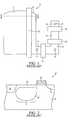
- FIG. 1A schematic top view of a portion of a semiconductor wafer fragment containing one exemplary CMOS pixel cell is shown in FIG. 1.
- the CMOS pixel cell 10is a four transistor (4T) cell.
- the CMOS pixel cell 10generally comprises a charge collection region 21 for collecting charges generated by light incident on the pixel, and a transfer gate 50 for transferring photoelectric charges from the collection region 21 to a sensing node, typically a floating diffusion region 25 .
- the floating diffusion region 25is electrically connected to the gate of an output source follower transistor 60 .
- the pixel cell 10also includes a reset transistor 40 for resetting the floating diffusion region 25 to a predetermined voltage before sensing a signal; a source follower transistor 60 which receives at its gate an electrical signal from the floating diffusion region 25 ; and a row select transistor 80 for outputting a signal from the source follower transistor 60 to an output terminal in response to an address signal.
- FIG. 2is a diagrammatic side sectional view of the pixel cell 10 of FIG. 1 taken along line A-A′.
- the exemplary CMOS pixel cell 10has a pinned photodiode (PPD) as the charge collection region 21 .
- PPDpinned photodiode
- the PPD 21is termed such since the potential in the photodiode is pinned to a constant value when the photodiode is fully depleted.
- the PPD 21is adjacent to the gate 50 of a transfer transistor.
- the PPD 21has a photosensitive or p-n-p junction region comprising a p-type surface layer 24 and an n-type photodiode region 26 within a p-type active layer 20 .
- CMOS image sensorssuch as the CMOS image sensor cell 10 of FIGS. 1-2
- incident lightcauses electrons to collect in region 26 .
- a maximum output signalwhich is produced by the source follower transistor having gate 60 , is proportional to the number of electrons to be extracted from the region 26 .
- the maximum output signalincreases with increased electron capacitance or acceptability of the region 26 to acquire electrons.
- the electron capacity of pinned photodiodestypically depends, among other factors, on the doping level of the image sensor and the dopants implanted into the active layer.
- the p-type layer 24 , the n-type region 26 and the floating diffusion region 25are formed within a doped well, for example a p-type well for NMOS transistors or an n-type well for PMOS transistors, located within substrate 20 .
- This wellis typically formed prior to the formation of the transfer gate 50 by implanting dopants of a predefined conductivity type within the substrate 20 .
- both the location and dopant concentration of the wellaffect critical parameters of CMOS imagers, such as dark current, lag and quantum efficiency. For example, if the p-type layer 24 , the n-type region 26 and the floating diffusion region 25 are all formed within the doped well, then the quantum efficiency of the imager decreases.
- the doped wellis masked only in the photodiode region so that the doped well extends below the transfer gate 50 and the floating diffusion region 25 , then the quantum efficiency is not affected, but the barrier to charge transfer between the photodiode and the transfer gate is undesirably increased.
- the doped wellis masked totally out of both the transfer gate and the photodiode region, then the transfer gate leakage undesirably increases.
- an improved active pixel photosensor for use in a CMOS imagerthat exhibits increased barrier control, improved quantum efficiency and improved leakage.
- a method of fabricating an active pixel photosensor exhibiting these improvementsis also needed, as well as a method of forming a doped well with optimized barrier control.
- the inventionprovides a well region of a first conductivity type located below at least a portion of an electrically active region of a transistor gate and laterally displaced from a charge collection region of a second conductivity type of a pinned photodiode.
- the well region of the first conductivity typeis located below about half of the electrically active portion of the transistor gate.
- the inventionprovides a well region of a first conductivity type which is located within a substrate of the first conductivity type, but which is totally masked from a photodiode region of a pixel sensor cell.
- the well region of the first conductivity typeis located below about half the length of the electrically active portion of a transistor gate and laterally displaced from a charge collection region of a second conductivity type of the photodiode.
- the inventionprovides a method of providing an improved charge transfer between a photodiode and a transistor gate, such as a transfer gate of a pixel sensor cell.
- a transistor gateis formed over a substrate of a first conductivity type.
- a well region of the first conductivity typeis formed below at least a portion of an electrically active region of the transistor gate and, preferably, subsequent to the formation of the transistor gate.
- the well regionis formed by implanting a dopant of the first conductivity type in an area of a substrate below about half the channel length of the electrically active portion of the transistor gate to form a doped region of a first dopant concentration.
- the doped regionis also laterally displaced from a charge collection region of a second conductivity type of a pinned photodiode, and having a second dopant concentration.
- a transistor gatefor example a transfer gate of a 4T pixel cell, is formed over a substrate of a first conductivity type.
- a maskis directly aligned with the transistor gate and patterned so that about half the length of the transistor gate and an active area where a photodiode is to be formed are masked.
- Ion implantationis next conducted to implant dopants of the first conductivity type below about half the length of the transistor gate and below an isolation region adjacent the active area, but not under the active area of the substrate where the photodiode is to be formed, forming a doped well region of the first conductivity type.
- a charge collection region of a second conductivity type of a photodiodeis formed laterally displaced from the well region of the first conductivity type.
- FIG. 1is a top plan view of an exemplary CMOS image sensor pixel.
- FIG. 2is a schematic cross-sectional view of the CMOS image sensor pixel of FIG. 1 taken along line 2 - 2 ′.
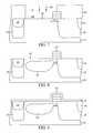
- FIG. 3is a schematic cross-sectional view of a CMOS image sensor pixel illustrating the fabrication of a doped well in accordance with an embodiment of the present invention and at an initial stage of processing.
- FIG. 4is a schematic cross-sectional view of a CMOS image sensor fragment of FIG. 3 at a stage of processing subsequent to that shown in FIG. 3.
- FIG. 5is a schematic cross-sectional view of a CMOS image sensor pixel of FIG. 3 at a stage of processing subsequent to that shown in FIG. 4.
- FIG. 6is a schematic cross-sectional view of a CMOS image sensor pixel of FIG. 3 at a stage of processing subsequent to that shown in FIG. 5.
- FIG. 7is a schematic cross-sectional view of a CMOS image sensor pixel of FIG. 3 at a stage of processing subsequent to that shown in FIG. 6.
- FIG. 8is a schematic cross-sectional view of a CMOS image sensor pixel of FIG. 3 at a stage of processing subsequent to that shown in FIG. 7.
- FIG. 9is a schematic cross-sectional view of a CMOS image sensor pixel of FIG. 3 at a stage of processing subsequent to that shown in FIG. 8.
- FIG. 10is a schematic cross-sectional view of a CMOS image sensor pixel of FIG. 3 at a stage of processing subsequent to that shown in FIG. 9.
- FIG. 11is a schematic cross-sectional view of a CMOS image sensor pixel of FIG. 3 at a stage of processing subsequent to that shown in FIG. 10.
- FIG. 12is a schematic diagram of the image sensor pixel of FIG. 11.
- FIG. 13is a schematic cross-sectional view of a CMOS image sensor pixel of FIG. 3 at a stage of processing subsequent to that shown in FIG. 4 and in accordance with a second embodiment of the invention.
- FIG. 14is a schematic diagram of the image sensor pixel of FIG. 13.
- FIG. 15is a schematic diagram of a 5T pixel sensor cell according to an embodiment of the present invention.
- FIG. 16illustrates a schematic diagram of a computer processor system incorporating a CMOS image sensor pixel fabricated according to the present invention.
- wafer and substrateare to be understood as a semiconductor-based material including silicon, silicon-on-insulator (SOI) or silicon-on-sapphire (SOS) technology, doped and undoped semiconductors, epitaxial layers of silicon supported by a base semiconductor foundation, and other semiconductor structures.
- SOIsilicon-on-insulator
- SOSsilicon-on-sapphire
- doped and undoped semiconductorsepitaxial layers of silicon supported by a base semiconductor foundation, and other semiconductor structures.
- previous process stepsmay have been utilized to form regions or junctions in or over the base semiconductor structure or foundation.
- the semiconductorneed not be silicon-based, but could be based on silicon-germanium, silicon-on-insulator, silicon-on-saphire, germanium, or gallium arsenide, among others.
- pixelrefers to a picture element unit cell containing a photosensor and transistors for converting electromagnetic radiation to an electrical signal.
- a representative pixelis illustrated in the figures and description herein and, typically, fabrication of all pixels in an imager will proceed simultaneously in a similar fashion.
- FIGS. 3-11illustrate a first exemplary embodiment of a method of forming a four-transistor (4T) pixel sensor cell 100 (FIG. 11) having a pinned photodiode 199 (FIG. 11) laterally displaced from a p-type well 120 formed below about half the length of gate stack 130 .
- 4Tfour-transistor
- FIG. 3illustrates a substrate 110 along a cross-sectional view which is the same view as in FIG. 2.
- the substrate 110is a silicon substrate lightly doped with a dopant of a first conductivity type, which for exemplary purposes is p-type.
- the dopant concentration in the p-type silicon substrate 110is within the range of about 1 ⁇ 10 14 to about 1 ⁇ 10 16 atoms per cm 3 , and is preferably within the range of about 5 ⁇ 10 14 to about 3 ⁇ 10 15 atoms per cm 3 .
- FIG. 3also illustrates isolation regions 155 which define a portion of a pixel.
- Isolation regions 155are preferably shallow trench isolation (STI) regions, having a depth of about 1,000 to about 4,000 Angstroms, more preferably of about 2,000 to about 3,500 Angstroms, and a width “W” of about 500 to about 10,000 Angstroms, more preferably of about 1,000 to about 8,000 Angstroms.
- isolation regions 155are formed as trenches which contain a blanket-deposited dielectric material, which may be an oxide material, for example a silicon oxide such as SiO or SiO 2 , oxynitride, a nitride material such as silicon nitride, silicon carbide, or other suitable dielectric materials.
- the dielectric materialis a high density plasma (HDP) oxide, a material which has a high ability to effectively fill narrow trenches.
- HDPhigh density plasma
- the transfer gate stack 130comprises a first gate oxide layer 131 of grown or deposited silicon oxide on the substrate 110 , a conductive layer 132 of doped polysilicon or other conductive material, and a second insulating layer 133 , which may be formed of, for example, silicon oxide (silicon dioxide), nitride (silicon nitride), oxynitride (silicon oxynitride), ON (oxide-nitride), NO (nitride-oxide), or ONO (oxide-nitride-oxide), or other insulating materials.
- the first and second insulating layers 131 , 133 and the conductive layer 132may be formed by conventional deposition methods, for example, chemical vapor deposition (CVD) or plasma enhanced chemical vapor deposition (PECVD), among many others.
- the transfer gate stack 130has a channel length “L” of about 500 Angstroms to about 10,000 Angstroms, more preferably of about 2,000 to about 8,000 Angstroms.
- a silicide layer(not shown) may be also formed in the multi-layered gate stack 130 , between the conductive layer 132 and the second insulating layer 133 .
- the gate structures of all other transistors in the imager circuit designmay have this additionally formed silicide layer.
- This silicide layermay be titanium silicide, tungsten silicide, cobalt silicide, molybdenum silicide, or tantalum silicide.
- the silicide layercould also be a barrier layer/refractory metal such as TiN/W or WN x /W or it could be entirely formed of WN x .
- a first photoresist layer 167is formed over the structure of FIG. 3 to a thickness of about 1,000 Angstroms to about 50,000 Angstroms, more preferably of about 10,000 Angstroms to about 45,000 Angstroms.
- the first photoresist layer 167is patterned to obtain two openings: a first opening 168 over an area 101 (FIG. 4) of the substrate 110 where a well region will be formed below at least a portion of transfer gate stack 130 ; and a second opening 166 over the left isolation region 155 of FIG. 4, in accordance with an embodiment of the present invention.
- the transistor immediate adjacent the photodiode in a 3T CMOS imageris the reset gate.
- the first photoresist layeris patterned over the reset transistor. In general, the patterning occurs over the transistor adjacent to the photodiode.
- the first photoresist layer 167is patterned so that, on one side of the first opening 168 , the photoresist layer 167 extends over the gate stack 130 by a distance “D 1 ” of about 250 Angstroms to about 5,000 Angstroms, more preferably of about 1,000 Angstroms to about 4,000 Angstroms, which represents about half of the channel length L of the transfer gate 130 .
- the photoresist layer 167is approximately coincident with the left side of right isolation region 155 of FIG. 5.
- the opening 166is smaller than the width W by about 0 to about 6,000 Angstroms, more preferably about 300 to about 3,000 Angstroms.
- FIG. 4is subjected to a first dopant implantation 169 (FIG. 5) with a dopant of the first conductivity type, which for exemplary purposes is p-type.
- a dopant of the first conductivity typewhich for exemplary purposes is p-type.
- p-type ionsare implanted through openings 166 , 168 and into areas 101 , 103 of the substrate 110 to form a p-type well region 120 , as illustrated in FIG. 6.
- the p-type well region 120extends below about half the length L of the gate stack 130 and is adjacent an active area 102 (FIG. 6) of the substrate 110 where a photodiode is to be formed, as will be described below.
- the p-type well region 120also extends below the left isolation region 155 of FIG. 6.
- the thickness T (FIG. 6) of the p-type well region 120is about 4,000 Angstroms to about 40,000 Angstroms, more preferably of about 10,000 Angstroms to about 30,000 Angstroms.
- the dopant implantation 169is conducted to implant p-type ions, such as boron or indium, into areas 101 and 103 of the substrate 110 located below about half the length L of the gate stack 130 and below the left isolation region 155 , to form the p-type well region 120 (FIG. 6).
- the ion implantation 169may be conducted at an energy of 50 keV to about 5 MeV, more preferably of about 100 keV to about 2 MeV.
- the implant dose in the p-type well 120is within the range of about 5 ⁇ 10 11 to about 5 ⁇ 10 13 atoms per cm 2 , and is preferably within the range of about 1 ⁇ 10 12 to about 5 ⁇ 10 12 atoms per cm 2 . If desired, multiple implants may be used to tailor the profile of the p-type well region 120 .
- a second masked dopant implantationis conducted with a dopant of a second conductivity type, which for exemplary purposes is n-type, to implant ions in the area of the substrate directly beneath the active area 102 of the pixel cell and to form an n-type region 126 , as illustrated in FIG. 8.
- a second photoresist layer 267is formed over the structure of FIG. 6 and patterned to obtain a third opening 268 , as shown in FIG. 7.
- the second photoresist layer 267is spaced away from the edge of the left STI region 155 of FIG. 7.
- the second photoresist layer 267just overlaps the left lateral edge of the gate stack 130 .
- the implanted n-doped region 126forms a photosensitive charge storage region for collecting photogenerated electrons which, on its right side, is laterally displaced from the p-type well 120 by an offset distance “ ⁇ ” (FIG. 8) of about 200 Angstroms to about 5,000 Angstroms, more preferably about 1,000 Angstroms to about 3,000 Angstroms, which represents just less than half of the channel length L of the transfer gate 130 (for a transfer gate channel of about 250 Angstroms to about 10,000 Angstroms, as noted above).
- ⁇offset distance
- Ion implantationmay be conducted by placing the substrate 110 in an ion implanter, and implanting appropriate n-type dopant ions into the substrate 110 at an energy of 10 keV to 1 MeV, more preferably 40 keV to 300 keV, to form the n-doped region 126 .
- N-type dopantssuch as arsenic, antimony, or phosphorous may be employed.
- the implant dose of the n-doped region 126(FIG. 8) is within the range of about 5 ⁇ 10 11 to about 1 ⁇ 10 13 atoms per cm 2 , and is preferably within the range of about 1 ⁇ 10 12 to about 5 ⁇ 10 12 atoms per cm 2 .
- multiple implantsmay be used to tailor the profile of the n-doped region 126 .
- the implants forming region 126may also be angled implants formed by angling the direction of implants 269 toward the gate stack 130 .
- the second photoresist layer 267is removed by conventional techniques, such as oxygen plasma for example.
- oxygen plasmafor example.
- An insulating layer 135is next formed over the substrate 110 including the p-type well region 120 , the STI regions 155 , and the gate stack 130 , as shown in FIG. 9.
- the insulating layer 135may be preferably an oxide, such as silicon dioxide, silicon nitride, silicon oxynitride, ON, NO, ONO or TEOS, among others.
- the insulating layer 135may be formed by an oxidation or a deposition method and to a thickness of about 20 Angstroms to about 1,500 Angstroms, more preferably of about 30 Angstroms to about 1,000 Angstroms.
- a third photoresist layer 367is formed over the structure of FIG. 9 and patterned to obtain a fourth opening 368 , as shown in FIG. 10.
- the third photoresist layer 367overlaps the left edge of the left STI region 155 of FIG. 10.
- the third photoresist layer 367overlaps the gate stack 130 .
- N-type floating diffusion region 125may be formed within the p-type well 120 before or after the formation of the structures of the photodiode 199 by methods known in the art.
- FIG. 12illustrates a schematic diagram of the pixel sensor cell 100 of FIG. 11. Conventional processing steps may be also employed to form contacts and wiring to connect gate lines and other connections in the pixel cell 100 .
- the entire surfacemay be covered with a passivation layer of, e.g., silicon dioxide, BSG, PSG, or BPSG, which is CMP planarized and etched to provide conductor holes, which are then metallized to provide contacts to the reset gate, transfer gate and other pixel gate structures, as needed.
- a passivation layere.g., silicon dioxide, BSG, PSG, or BPSG
- Conventional multiple layers of conductors and insulators to other circuit structuresmay also be used to interconnect the structures of the pixel sensor cell.
- FIGS. 13-14illustrate a 3T pixel sensor cell 300 comprising a p-type well region 320 formed below about half the length of reset gate stack 230 of a reset transistor.
- the 3 T pixel sensor cell 300differs from the 4T cell 100 by the omission of the charge transfer transistor and associated gate 130 .
- the n-region 126 b of photodiode 399 and the Vdd diffusion region 325are coupled through the reset transistor 230 .
- the p-type well region 320is adjacent an active area 102 (FIG. 13) of the substrate 110 where photodiode 399 is formed.
- the p-type well region 320also extends below the drain region 325 formed adjacent the reset gate stack 230 and below both isolation regions 155 , as shown in FIG. 13.
- Region 325is a more highly doped region to enable low contact resistance between the photodiode n-type region 126 b to the source follower gate 60 through a contact to the 325 diffusion (not shown).
- FIG. 15illustrates a five-transistor (5T) cell 400 comprising a p-type well region formed below at least a portion of a transfer transistor 130 , in accordance with another embodiment of the present invention.
- the 5T cell 400differs from the 4T cell 100 of FIGS. 11-12 by the addition of a shutter transistor 430 (FIG. 15).
- An imager device 640 containing a pixel array having pixels as constructed abovemay be coupled to a processor system.
- a typical processor systemwhich includes a CMOS image sensor 642 according to the invention is illustrated in FIG. 16. Without being limiting, such a system could include a computer system, camera system, scanner, machine vision, vehicle navigation, video phone, and surveillance system, all of which can utilize the present invention.
- a processor based systemsuch as a computer system, for example generally comprises a central processing unit (CPU) 644 , for example, a microprocessor, that communicates with an input/output (I/O) device 646 over a bus 652 .
- the CMOS image sensor 642also communicates with the system over bus 652 .
- the computer system 600also includes random access memory (RAM) 648 , and, in the case of a computer system may include peripheral devices such as a floppy disk drive 654 , and a compact disk (CD) ROM drive 656 or a flash memory card 657 which also communicate with CPU 644 over the bus 652 . It may also be desirable to integrate the processor 654 , CMOS image sensor 642 and memory 648 on a single IC chip.
- the embodiments of the inventionhave been described with reference to the formation of a p-n-p photodiode, such as the p-n-p photodiode 199 , 399 (FIGS. 11 and 13) and a p-type well region 120 , 320 formed below at least a portion of an active region of a transistor gate stack, it must be understood that the invention is not limited to this embodiment. Accordingly, the invention has equal applicability to complementary structures employing n-p-n photodiodes and an n-type well region 120 , 320 formed by the above-described methods. Of course, the dopant and conductivity type of all structures will change accordingly, with the transfer gate corresponding to a PMOS transistor.
Landscapes
- Solid State Image Pick-Up Elements (AREA)
Abstract
Description
- This application claims priority to U.S. Provisional Patent Application No. 60/478,350 filed on Jun. 16, 2003 which is hereby incorporated by reference in its entirety.[0001]
- The present invention relates to the field of semiconductor devices and, in particular, to improved high quantum efficiency imagers.[0002]
- CMOS imagers are increasingly being used as low cost imaging devices. A CMOS image sensor circuit includes a focal plane array of pixel cells, each one of the cells including a photogate, photoconductor, or photodiode overlying a charge accumulation region within a substrate for accumulating photo-generated charge. Each pixel cell may include a transistor for transferring charge from the charge accumulation region to a sensing node, and a transistor for resetting a sensing node to a predetermined charge level prior to charge transference. The pixel cell may also include a source follower transistor for receiving and amplifying charge from the sensing node and an access transistor for controlling the readout of the cell contents from the source follower transistor.[0003]
- In a CMOS image sensor, the active elements of a pixel cell perform the necessary functions of: (1) photon to charge conversion; (2) accumulation of image charge; (3) transfer of charge to the sensing node accompanied by charge amplification; (4) resetting the sensing node to a known state before the transfer of charge to it; (5) selection of a pixel for readout; and (6) output and amplification of a signal representing pixel charge from the sensing node. Photo-generated charge may be amplified when it moves from the initial charge accumulation region to the sensing node. The charge at the sensing node is typically converted to a pixel output voltage by a source follower output transistor.[0004]
- A schematic top view of a portion of a semiconductor wafer fragment containing one exemplary CMOS pixel cell is shown in FIG. 1. The[0005]
CMOS pixel cell 10 is a four transistor (4T) cell. TheCMOS pixel cell 10 generally comprises acharge collection region 21 for collecting charges generated by light incident on the pixel, and atransfer gate 50 for transferring photoelectric charges from thecollection region 21 to a sensing node, typically afloating diffusion region 25. Thefloating diffusion region 25 is electrically connected to the gate of an outputsource follower transistor 60. Thepixel cell 10 also includes areset transistor 40 for resetting thefloating diffusion region 25 to a predetermined voltage before sensing a signal; asource follower transistor 60 which receives at its gate an electrical signal from thefloating diffusion region 25; and a rowselect transistor 80 for outputting a signal from thesource follower transistor 60 to an output terminal in response to an address signal. - FIG. 2 is a diagrammatic side sectional view of the[0006]
pixel cell 10 of FIG. 1 taken along line A-A′. As shown in FIG. 2, the exemplaryCMOS pixel cell 10 has a pinned photodiode (PPD) as thecharge collection region 21. ThePPD 21 is termed such since the potential in the photodiode is pinned to a constant value when the photodiode is fully depleted. ThePPD 21 is adjacent to thegate 50 of a transfer transistor. ThePPD 21 has a photosensitive or p-n-p junction region comprising a p-type surface layer 24 and an n-type photodiode region 26 within a p-typeactive layer 20. - Generally, in CMOS image sensors such as the CMOS[0007]
image sensor cell 10 of FIGS. 1-2, incident light causes electrons to collect inregion 26. A maximum output signal, which is produced by the source followertransistor having gate 60, is proportional to the number of electrons to be extracted from theregion 26. The maximum output signal increases with increased electron capacitance or acceptability of theregion 26 to acquire electrons. The electron capacity of pinned photodiodes typically depends, among other factors, on the doping level of the image sensor and the dopants implanted into the active layer. - Typically, the p-[0008]
type layer 24, the n-type region 26 and thefloating diffusion region 25 are formed within a doped well, for example a p-type well for NMOS transistors or an n-type well for PMOS transistors, located withinsubstrate 20. This well is typically formed prior to the formation of thetransfer gate 50 by implanting dopants of a predefined conductivity type within thesubstrate 20. As known in the art, both the location and dopant concentration of the well affect critical parameters of CMOS imagers, such as dark current, lag and quantum efficiency. For example, if the p-type layer 24, the n-type region 26 and thefloating diffusion region 25 are all formed within the doped well, then the quantum efficiency of the imager decreases. If, however, the doped well is masked only in the photodiode region so that the doped well extends below thetransfer gate 50 and thefloating diffusion region 25, then the quantum efficiency is not affected, but the barrier to charge transfer between the photodiode and the transfer gate is undesirably increased. Alternatively, if the doped well is masked totally out of both the transfer gate and the photodiode region, then the transfer gate leakage undesirably increases. - Accordingly, there is needed an improved active pixel photosensor for use in a CMOS imager that exhibits increased barrier control, improved quantum efficiency and improved leakage. A method of fabricating an active pixel photosensor exhibiting these improvements is also needed, as well as a method of forming a doped well with optimized barrier control.[0009]
- In one aspect, the invention provides a well region of a first conductivity type located below at least a portion of an electrically active region of a transistor gate and laterally displaced from a charge collection region of a second conductivity type of a pinned photodiode. Preferably, the well region of the first conductivity type is located below about half of the electrically active portion of the transistor gate.[0010]
- In another aspect, the invention provides a well region of a first conductivity type which is located within a substrate of the first conductivity type, but which is totally masked from a photodiode region of a pixel sensor cell. Preferably, the well region of the first conductivity type is located below about half the length of the electrically active portion of a transistor gate and laterally displaced from a charge collection region of a second conductivity type of the photodiode.[0011]
- In another aspect, the invention provides a method of providing an improved charge transfer between a photodiode and a transistor gate, such as a transfer gate of a pixel sensor cell. A transistor gate is formed over a substrate of a first conductivity type. A well region of the first conductivity type is formed below at least a portion of an electrically active region of the transistor gate and, preferably, subsequent to the formation of the transistor gate. In one embodiment, the well region is formed by implanting a dopant of the first conductivity type in an area of a substrate below about half the channel length of the electrically active portion of the transistor gate to form a doped region of a first dopant concentration. The doped region is also laterally displaced from a charge collection region of a second conductivity type of a pinned photodiode, and having a second dopant concentration.[0012]
- In another embodiment, a transistor gate, for example a transfer gate of a 4T pixel cell, is formed over a substrate of a first conductivity type. A mask is directly aligned with the transistor gate and patterned so that about half the length of the transistor gate and an active area where a photodiode is to be formed are masked. Ion implantation is next conducted to implant dopants of the first conductivity type below about half the length of the transistor gate and below an isolation region adjacent the active area, but not under the active area of the substrate where the photodiode is to be formed, forming a doped well region of the first conductivity type. A charge collection region of a second conductivity type of a photodiode is formed laterally displaced from the well region of the first conductivity type.[0013]
- By providing a lateral impurity gradient and a corresponding potential gradient that favors photogenerated electron movement from the charge collection region of the photodiode, under the transistor gate, and to a floating diffusion node, potential barriers are less likely to form and more complete charge transfer and lower voltage operation are facilitated.[0014]
- These and other features of the invention will be more apparent from the following detailed description that is provided in connection with the accompanying drawings and illustrated exemplary embodiments of the invention.[0015]
- FIG. 1 is a top plan view of an exemplary CMOS image sensor pixel.[0016]
- FIG. 2 is a schematic cross-sectional view of the CMOS image sensor pixel of FIG. 1 taken along line[0017]2-2′.
- FIG. 3 is a schematic cross-sectional view of a CMOS image sensor pixel illustrating the fabrication of a doped well in accordance with an embodiment of the present invention and at an initial stage of processing.[0018]
- FIG. 4 is a schematic cross-sectional view of a CMOS image sensor fragment of FIG. 3 at a stage of processing subsequent to that shown in FIG. 3.[0019]
- FIG. 5 is a schematic cross-sectional view of a CMOS image sensor pixel of FIG. 3 at a stage of processing subsequent to that shown in FIG. 4.[0020]
- FIG. 6 is a schematic cross-sectional view of a CMOS image sensor pixel of FIG. 3 at a stage of processing subsequent to that shown in FIG. 5.[0021]
- FIG. 7 is a schematic cross-sectional view of a CMOS image sensor pixel of FIG. 3 at a stage of processing subsequent to that shown in FIG. 6.[0022]
- FIG. 8 is a schematic cross-sectional view of a CMOS image sensor pixel of FIG. 3 at a stage of processing subsequent to that shown in FIG. 7.[0023]
- FIG. 9 is a schematic cross-sectional view of a CMOS image sensor pixel of FIG. 3 at a stage of processing subsequent to that shown in FIG. 8.[0024]
- FIG. 10 is a schematic cross-sectional view of a CMOS image sensor pixel of FIG. 3 at a stage of processing subsequent to that shown in FIG. 9.[0025]
- FIG. 11 is a schematic cross-sectional view of a CMOS image sensor pixel of FIG. 3 at a stage of processing subsequent to that shown in FIG. 10.[0026]
- FIG. 12 is a schematic diagram of the image sensor pixel of FIG. 11.[0027]
- FIG. 13 is a schematic cross-sectional view of a CMOS image sensor pixel of FIG. 3 at a stage of processing subsequent to that shown in FIG. 4 and in accordance with a second embodiment of the invention.[0028]
- FIG. 14 is a schematic diagram of the image sensor pixel of FIG. 13.[0029]
- FIG. 15 is a schematic diagram of a 5T pixel sensor cell according to an embodiment of the present invention.[0030]
- FIG. 16 illustrates a schematic diagram of a computer processor system incorporating a CMOS image sensor pixel fabricated according to the present invention.[0031]
- In the following detailed description, reference is made to the accompanying drawings which form a part hereof, and in which is shown by way of illustration specific embodiments in which the invention may be practiced. These embodiments are described in sufficient detail to enable those skilled in the art to practice the invention, and it is to be understood that other embodiments may be utilized, and that structural, logical and electrical changes may be made without departing from the spirit and scope of the present invention.[0032]
- The terms “wafer” and “substrate” are to be understood as a semiconductor-based material including silicon, silicon-on-insulator (SOI) or silicon-on-sapphire (SOS) technology, doped and undoped semiconductors, epitaxial layers of silicon supported by a base semiconductor foundation, and other semiconductor structures. Furthermore, when reference is made to a “wafer” or “substrate” in the following description, previous process steps may have been utilized to form regions or junctions in or over the base semiconductor structure or foundation. In addition, the semiconductor need not be silicon-based, but could be based on silicon-germanium, silicon-on-insulator, silicon-on-saphire, germanium, or gallium arsenide, among others.[0033]
- The term “pixel” refers to a picture element unit cell containing a photosensor and transistors for converting electromagnetic radiation to an electrical signal. For purposes of illustration, a representative pixel is illustrated in the figures and description herein and, typically, fabrication of all pixels in an imager will proceed simultaneously in a similar fashion.[0034]
- Referring now to the drawings, where like elements are designated by like reference numerals, FIGS. 3-11 illustrate a first exemplary embodiment of a method of forming a four-transistor (4T) pixel sensor cell[0035]100 (FIG. 11) having a pinned photodiode199 (FIG. 11) laterally displaced from a p-type well120 formed below about half the length of
gate stack 130. - FIG. 3 illustrates a[0036]
substrate 110 along a cross-sectional view which is the same view as in FIG. 2. For exemplary purposes, thesubstrate 110 is a silicon substrate lightly doped with a dopant of a first conductivity type, which for exemplary purposes is p-type. However, as noted above, the invention has equal application to other semiconductor substrates and to complementary structures. The dopant concentration in the p-type silicon substrate 110 is within the range of about 1×10¹⁴to about 1×10¹⁶atoms per cm3, and is preferably within the range of about 5×10¹⁴to about 3×10¹⁵atoms per cm3. - FIG. 3 also illustrates[0037]
isolation regions 155 which define a portion of a pixel.Isolation regions 155 are preferably shallow trench isolation (STI) regions, having a depth of about 1,000 to about 4,000 Angstroms, more preferably of about 2,000 to about 3,500 Angstroms, and a width “W” of about 500 to about 10,000 Angstroms, more preferably of about 1,000 to about 8,000 Angstroms. Preferably,isolation regions 155 are formed as trenches which contain a blanket-deposited dielectric material, which may be an oxide material, for example a silicon oxide such as SiO or SiO2, oxynitride, a nitride material such as silicon nitride, silicon carbide, or other suitable dielectric materials. In a preferred embodiment, the dielectric material is a high density plasma (HDP) oxide, a material which has a high ability to effectively fill narrow trenches. - Also illustrated in FIG. 3 is a multi-layered[0038]
transfer gate stack 130 formed over thesubstrate 110. Thetransfer gate stack 130 comprises a firstgate oxide layer 131 of grown or deposited silicon oxide on thesubstrate 110, aconductive layer 132 of doped polysilicon or other conductive material, and a second insulatinglayer 133, which may be formed of, for example, silicon oxide (silicon dioxide), nitride (silicon nitride), oxynitride (silicon oxynitride), ON (oxide-nitride), NO (nitride-oxide), or ONO (oxide-nitride-oxide), or other insulating materials. The first and second insulatinglayers conductive layer 132 may be formed by conventional deposition methods, for example, chemical vapor deposition (CVD) or plasma enhanced chemical vapor deposition (PECVD), among many others. Thetransfer gate stack 130 has a channel length “L” of about 500 Angstroms to about 10,000 Angstroms, more preferably of about 2,000 to about 8,000 Angstroms. - If desired, a silicide layer (not shown) may be also formed in the[0039]
multi-layered gate stack 130, between theconductive layer 132 and the second insulatinglayer 133. Advantageously, the gate structures of all other transistors in the imager circuit design may have this additionally formed silicide layer. This silicide layer may be titanium silicide, tungsten silicide, cobalt silicide, molybdenum silicide, or tantalum silicide. The silicide layer could also be a barrier layer/refractory metal such as TiN/W or WNx/W or it could be entirely formed of WNx. - Referring now to FIG. 4, subsequent to the formation of the[0040]
isolation regions 155 and of thegate stack 130, afirst photoresist layer 167 is formed over the structure of FIG. 3 to a thickness of about 1,000 Angstroms to about 50,000 Angstroms, more preferably of about 10,000 Angstroms to about 45,000 Angstroms. Thefirst photoresist layer 167 is patterned to obtain two openings: afirst opening 168 over an area101 (FIG. 4) of thesubstrate 110 where a well region will be formed below at least a portion oftransfer gate stack 130; and asecond opening 166 over theleft isolation region 155 of FIG. 4, in accordance with an embodiment of the present invention. - As another example, the transistor immediate adjacent the photodiode in a 3T CMOS imager is the reset gate. Thus, in the case of 3T CMOS pixels, the first photoresist layer is patterned over the reset transistor. In general, the patterning occurs over the transistor adjacent to the photodiode.[0041]
- As illustrated in FIG. 4, the[0042]
first photoresist layer 167 is patterned so that, on one side of thefirst opening 168, thephotoresist layer 167 extends over thegate stack 130 by a distance “D1” of about 250 Angstroms to about 5,000 Angstroms, more preferably of about 1,000 Angstroms to about 4,000 Angstroms, which represents about half of the channel length L of thetransfer gate 130. On the other side of theopening 168, thephotoresist layer 167 is approximately coincident with the left side ofright isolation region 155 of FIG. 5. Preferably, theopening 166 is smaller than the width W by about 0 to about 6,000 Angstroms, more preferably about 300 to about 3,000 Angstroms. - Next, the structure of FIG. 4 is subjected to a first dopant implantation[0043]169 (FIG. 5) with a dopant of the first conductivity type, which for exemplary purposes is p-type. This way, p-type ions are implanted through
openings areas substrate 110 to form a p-type well region 120, as illustrated in FIG. 6. The p-type well region 120 extends below about half the length L of thegate stack 130 and is adjacent an active area102 (FIG. 6) of thesubstrate 110 where a photodiode is to be formed, as will be described below. The p-type well region 120 also extends below theleft isolation region 155 of FIG. 6. The thickness T (FIG. 6) of the p-type well region 120, or the depth of the of the p-type well region 120 below thegate stack 130, is about 4,000 Angstroms to about 40,000 Angstroms, more preferably of about 10,000 Angstroms to about 30,000 Angstroms. - The[0044]
dopant implantation 169 is conducted to implant p-type ions, such as boron or indium, intoareas substrate 110 located below about half the length L of thegate stack 130 and below theleft isolation region 155, to form the p-type well region120 (FIG. 6). Theion implantation 169 may be conducted at an energy of 50 keV to about 5 MeV, more preferably of about 100 keV to about 2 MeV. The implant dose in the p-type well 120 is within the range of about 5×10¹¹to about 5×10¹³atoms per cm2, and is preferably within the range of about 1×10¹²to about 5×10¹²atoms per cm2. If desired, multiple implants may be used to tailor the profile of the p-type well region 120. - Subsequent to, or before, the formation of the p-[0045]
type well region 120 shown in FIG. 6, a second masked dopant implantation is conducted with a dopant of a second conductivity type, which for exemplary purposes is n-type, to implant ions in the area of the substrate directly beneath theactive area 102 of the pixel cell and to form an n-type region 126, as illustrated in FIG. 8. For this, asecond photoresist layer 267 is formed over the structure of FIG. 6 and patterned to obtain athird opening 268, as shown in FIG. 7. On one side of theopening 268, thesecond photoresist layer 267 is spaced away from the edge of theleft STI region 155 of FIG. 7. On the other side of theopening 268, thesecond photoresist layer 267 just overlaps the left lateral edge of thegate stack 130. - The implanted n-doped[0046]
region 126 forms a photosensitive charge storage region for collecting photogenerated electrons which, on its right side, is laterally displaced from the p-type well120 by an offset distance “Δ” (FIG. 8) of about 200 Angstroms to about 5,000 Angstroms, more preferably about 1,000 Angstroms to about 3,000 Angstroms, which represents just less than half of the channel length L of the transfer gate130 (for a transfer gate channel of about 250 Angstroms to about 10,000 Angstroms, as noted above). - Ion implantation may be conducted by placing the[0047]
substrate 110 in an ion implanter, and implanting appropriate n-type dopant ions into thesubstrate 110 at an energy of 10 keV to 1 MeV, more preferably 40 keV to 300 keV, to form the n-dopedregion 126. N-type dopants such as arsenic, antimony, or phosphorous may be employed. The implant dose of the n-doped region126 (FIG. 8) is within the range of about 5×10¹¹to about 1×10¹³atoms per cm2, and is preferably within the range of about 1×10¹²to about 5×10¹²atoms per cm2. If desired, multiple implants may be used to tailor the profile of the n-dopedregion 126. Theimplants forming region 126 may also be angled implants formed by angling the direction ofimplants 269 toward thegate stack 130. - Subsequent to the second dopant implantation[0048]269 (FIG. 7), the
second photoresist layer 267 is removed by conventional techniques, such as oxygen plasma for example. The structure at this point is depicted in FIG. 8. - An insulating[0049]
layer 135 is next formed over thesubstrate 110 including the p-type well region 120, theSTI regions 155, and thegate stack 130, as shown in FIG. 9. The insulatinglayer 135 may be preferably an oxide, such as silicon dioxide, silicon nitride, silicon oxynitride, ON, NO, ONO or TEOS, among others. The insulatinglayer 135 may be formed by an oxidation or a deposition method and to a thickness of about 20 Angstroms to about 1,500 Angstroms, more preferably of about 30 Angstroms to about 1,000 Angstroms. - Next, a[0050]
third photoresist layer 367 is formed over the structure of FIG. 9 and patterned to obtain afourth opening 368, as shown in FIG. 10. On one side of theopening 368, thethird photoresist layer 367 overlaps the left edge of theleft STI region 155 of FIG. 10. On the other side of theopening 368, thethird photoresist layer 367 overlaps thegate stack 130. - A third dopant implantation with a dopant of the first conductivity type, which for exemplary purposes is p-type, is conducted so that p-type ions are implanted into the[0051]
area 102 of the substrate over the implanted n-type region 126 and between thetransfer gate 130 and theisolation region 155, to form a p-type surface layer 124 of the now completed photodiode199 (FIG. 11) formed byregions photodiode 199 by methods known in the art. - After or during the formation of the[0052]
trench isolation regions 155, p-type well 120 and photodiode regions shown in the embodiments of FIG. 11, the remaining devices of thepixel sensor cell 100 including the reset transistor, the source follower transistor and row select transistor shown in FIG. 1 as associated withrespective gates pixel sensor cell 100 of FIG. 11. Conventional processing steps may be also employed to form contacts and wiring to connect gate lines and other connections in thepixel cell 100. For example, the entire surface may be covered with a passivation layer of, e.g., silicon dioxide, BSG, PSG, or BPSG, which is CMP planarized and etched to provide conductor holes, which are then metallized to provide contacts to the reset gate, transfer gate and other pixel gate structures, as needed. Conventional multiple layers of conductors and insulators to other circuit structures may also be used to interconnect the structures of the pixel sensor cell. - Although the invention has been described above with reference to a transfer gate of a transfer transistor for use in a four-transistor (4T) pixel cell of a CMOS imager, the invention also applies to CCD imagers.[0053]
- In addition, although the invention has been described above with reference to a transfer gate of a transfer transistor for use in a four-transistor (4T) pixel cell, the invention also has applicability to a three-transistor (3T) cell or a five-transistor (5T) cell. For example, FIGS. 13-14 illustrate a 3T[0054]
pixel sensor cell 300 comprising a p-type well region 320 formed below about half the length ofreset gate stack 230 of a reset transistor. As known in the art, the3Tpixel sensor cell 300 differs from the4T cell 100 by the omission of the charge transfer transistor and associatedgate 130. The n-region 126bofphotodiode 399 and theVdd diffusion region 325 are coupled through thereset transistor 230. The p-type well region 320 is adjacent an active area102 (FIG. 13) of thesubstrate 110 wherephotodiode 399 is formed. The p-type well region 320 also extends below thedrain region 325 formed adjacent thereset gate stack 230 and below bothisolation regions 155, as shown in FIG. 13.Region 325 is a more highly doped region to enable low contact resistance between the photodiode n-type region 126bto thesource follower gate 60 through a contact to the325 diffusion (not shown). - FIG. 15 illustrates a five-transistor (5T)[0055]
cell 400 comprising a p-type well region formed below at least a portion of atransfer transistor 130, in accordance with another embodiment of the present invention. The5T cell 400 differs from the4T cell 100 of FIGS. 11-12 by the addition of a shutter transistor430 (FIG. 15). - An imager device[0056]640 containing a pixel array having pixels as constructed above may be coupled to a processor system. A typical processor system, which includes a
CMOS image sensor 642 according to the invention is illustrated in FIG. 16. Without being limiting, such a system could include a computer system, camera system, scanner, machine vision, vehicle navigation, video phone, and surveillance system, all of which can utilize the present invention. - A processor based system, such as a computer system, for example generally comprises a central processing unit (CPU)[0057]644, for example, a microprocessor, that communicates with an input/output (I/O)
device 646 over abus 652. TheCMOS image sensor 642 also communicates with the system overbus 652. Thecomputer system 600 also includes random access memory (RAM)648, and, in the case of a computer system may include peripheral devices such as afloppy disk drive 654, and a compact disk (CD)ROM drive 656 or a flash memory card657 which also communicate withCPU 644 over thebus 652. It may also be desirable to integrate theprocessor 654,CMOS image sensor 642 andmemory 648 on a single IC chip. - Although the embodiments of the invention have been described with reference to the formation of a p-n-p photodiode, such as the[0058]
p-n-p photodiode 199,399 (FIGS. 11 and 13) and a p-type well region type well region - Further, although the embodiments of the invention have been described with reference to the formation of the p-[0059]
type well region gate stack type well region gate stack - The above description and drawings are only to be considered illustrative of exemplary embodiments, which achieve the features and advantages of the invention. Modification and substitutions to specific process conditions and structures can be made without departing from the spirit and scope of the invention. Accordingly, the invention is not to be considered as being limited by the foregoing description and drawings, but is only limited by the scope of the appended claims.[0060]
Claims (82)
Priority Applications (5)
| Application Number | Priority Date | Filing Date | Title |
|---|---|---|---|
| US10/648,378US6897082B2 (en) | 2003-06-16 | 2003-08-27 | Method of forming well for CMOS imager |
| US11/025,960US7190041B2 (en) | 2003-06-16 | 2005-01-03 | Well for CMOS imager |
| US11/105,419US7635604B2 (en) | 2003-06-16 | 2005-04-14 | Well for CMOS imager and method of formation |
| US11/636,658US7511354B2 (en) | 2003-06-16 | 2006-12-11 | Well for CMOS imager and method of formation |
| US12/402,226US7847366B2 (en) | 2003-06-16 | 2009-03-11 | Well for CMOS imager |
Applications Claiming Priority (2)
| Application Number | Priority Date | Filing Date | Title |
|---|---|---|---|
| US47835003P | 2003-06-16 | 2003-06-16 | |
| US10/648,378US6897082B2 (en) | 2003-06-16 | 2003-08-27 | Method of forming well for CMOS imager |
Related Child Applications (2)
| Application Number | Title | Priority Date | Filing Date |
|---|---|---|---|
| US11/025,960DivisionUS7190041B2 (en) | 2003-06-16 | 2005-01-03 | Well for CMOS imager |
| US11/105,419ContinuationUS7635604B2 (en) | 2003-06-16 | 2005-04-14 | Well for CMOS imager and method of formation |
Publications (2)
| Publication Number | Publication Date |
|---|---|
| US20040253761A1true US20040253761A1 (en) | 2004-12-16 |
| US6897082B2 US6897082B2 (en) | 2005-05-24 |
Family
ID=33514228
Family Applications (5)
| Application Number | Title | Priority Date | Filing Date |
|---|---|---|---|
| US10/648,378Expired - LifetimeUS6897082B2 (en) | 2003-06-16 | 2003-08-27 | Method of forming well for CMOS imager |
| US11/025,960Expired - LifetimeUS7190041B2 (en) | 2003-06-16 | 2005-01-03 | Well for CMOS imager |
| US11/105,419Expired - LifetimeUS7635604B2 (en) | 2003-06-16 | 2005-04-14 | Well for CMOS imager and method of formation |
| US11/636,658Expired - LifetimeUS7511354B2 (en) | 2003-06-16 | 2006-12-11 | Well for CMOS imager and method of formation |
| US12/402,226Expired - LifetimeUS7847366B2 (en) | 2003-06-16 | 2009-03-11 | Well for CMOS imager |
Family Applications After (4)
| Application Number | Title | Priority Date | Filing Date |
|---|---|---|---|
| US11/025,960Expired - LifetimeUS7190041B2 (en) | 2003-06-16 | 2005-01-03 | Well for CMOS imager |
| US11/105,419Expired - LifetimeUS7635604B2 (en) | 2003-06-16 | 2005-04-14 | Well for CMOS imager and method of formation |
| US11/636,658Expired - LifetimeUS7511354B2 (en) | 2003-06-16 | 2006-12-11 | Well for CMOS imager and method of formation |
| US12/402,226Expired - LifetimeUS7847366B2 (en) | 2003-06-16 | 2009-03-11 | Well for CMOS imager |
Country Status (1)
| Country | Link |
|---|---|
| US (5) | US6897082B2 (en) |
Cited By (19)
| Publication number | Priority date | Publication date | Assignee | Title |
|---|---|---|---|---|
| US20060255372A1 (en)* | 2005-05-16 | 2006-11-16 | Micron Technology, Inc. | Color pixels with anti-blooming isolation and method of formation |
| US20060276014A1 (en)* | 2005-06-07 | 2006-12-07 | Taiwan Semiconductor Manufacturing Co., Ltd. | Self-aligned high-energy implantation for deep junction structure |
| US20070018264A1 (en)* | 2005-07-22 | 2007-01-25 | Omnivision Technologies, Inc. | Optimized image sensor process and structure to improve blooming |
| US20070045679A1 (en)* | 2005-08-26 | 2007-03-01 | Micron Technology, Inc. | Implanted isolation region for imager pixels |
| US20070145443A1 (en)* | 2005-12-28 | 2007-06-28 | Keun Hyuk Lim | CMOS Image Sensor and Method of Manufacturing the Same |
| US20080197389A1 (en)* | 2004-07-29 | 2008-08-21 | Jae-Young Park | Image sensor with improved charge transfer efficiency and method for fabricating the same |
| CN100438060C (en)* | 2005-08-30 | 2008-11-26 | 台湾积体电路制造股份有限公司 | Semiconductor device and method of forming the same |
| US7528427B2 (en) | 2007-01-30 | 2009-05-05 | International Business Machines Corporation | Pixel sensor cell having asymmetric transfer gate with reduced pinning layer barrier potential |
| US20100184242A1 (en)* | 2009-01-16 | 2010-07-22 | Taiwan Semiconductor Manufacturing Company, Ltd. | Method of implantation |
| US20100308213A1 (en)* | 2009-05-07 | 2010-12-09 | Daniel Durini Romero | Detector |
| CN102299163A (en)* | 2011-09-13 | 2011-12-28 | 上海中科高等研究院 | Image sensor |
| US8129764B2 (en) | 2008-06-11 | 2012-03-06 | Aptina Imaging Corporation | Imager devices having differing gate stack sidewall spacers, method for forming such imager devices, and systems including such imager devices |
| US20120077301A1 (en)* | 2010-09-29 | 2012-03-29 | Samsung Electronics Co., Ltd. | Image sensor and method of fabricating the same |
| CN102446852A (en)* | 2011-09-08 | 2012-05-09 | 上海华力微电子有限公司 | Method used for integrating deep junction depth device and shallow junction depth device |
| US20140312391A1 (en)* | 2013-04-23 | 2014-10-23 | Samsung Electronics Co., Ltd. | Image sensor |
| CN107068703A (en)* | 2016-01-12 | 2017-08-18 | 三星电子株式会社 | Imaging sensor |
| CN107895732A (en)* | 2017-11-10 | 2018-04-10 | 中国电子科技集团公司第四十四研究所 | The CCD of big full-well capacity |
| US20190098236A1 (en)* | 2015-07-31 | 2019-03-28 | Sony Semiconductor Solutions Corporation | Solid-state image pickup device and electronic apparatus |
| CN110672202A (en)* | 2019-09-18 | 2020-01-10 | 上海奕瑞光电子科技股份有限公司 | Flat panel detector pixel circuit, flat panel detection system and flat panel detection method |
Families Citing this family (29)
| Publication number | Priority date | Publication date | Assignee | Title |
|---|---|---|---|---|
| KR100477790B1 (en)* | 2003-03-13 | 2005-03-22 | 매그나칩 반도체 유한회사 | Method of manufacturing cmos image sensor |
| KR100544957B1 (en)* | 2003-09-23 | 2006-01-24 | 동부아남반도체 주식회사 | Manufacturing Method of CMOS Image Sensor |
| US7354789B2 (en)* | 2003-11-04 | 2008-04-08 | Dongbu Electronics Co., Ltd. | CMOS image sensor and method for fabricating the same |
| US7348651B2 (en)* | 2004-12-09 | 2008-03-25 | Taiwan Semiconductor Manufacturing Co., Ltd. | Pinned photodiode fabricated with shallow trench isolation |
| US20060130042A1 (en)* | 2004-12-15 | 2006-06-15 | Dias Daniel M | Method and apparatus for dynamic application upgrade in cluster and grid systems for supporting service level agreements |
| KR100672669B1 (en)* | 2004-12-29 | 2007-01-24 | 동부일렉트로닉스 주식회사 | CMS image sensor and its manufacturing method |
| KR100746222B1 (en)* | 2005-07-11 | 2007-08-03 | 삼성전자주식회사 | Manufacturing Methods of Image Sensors |
| KR100672729B1 (en)* | 2005-07-14 | 2007-01-24 | 동부일렉트로닉스 주식회사 | Manufacturing Method of CMOS Image Sensor |
| KR100619549B1 (en)* | 2005-09-13 | 2006-09-01 | (주)한비젼 | Photodiode manufacturing method of an image sensor using a multilayer substrate, its contact method and its structure |
| KR100731099B1 (en)* | 2005-12-28 | 2007-06-22 | 동부일렉트로닉스 주식회사 | CMOS image sensor and its manufacturing method |
| US20080124830A1 (en)* | 2006-11-29 | 2008-05-29 | Sang-Gi Lee | Method of manufacturing image sensor |
| JP4420039B2 (en)* | 2007-02-16 | 2010-02-24 | ソニー株式会社 | Solid-state imaging device |
| US7459668B2 (en)* | 2007-03-06 | 2008-12-02 | Micron Technology, Inc. | Method, apparatus, and system to reduce ground resistance in a pixel array |
| US7642608B2 (en)* | 2007-03-09 | 2010-01-05 | Aptina Imaging Corporation | Dual isolation for image sensors |
| US7724293B2 (en)* | 2007-03-12 | 2010-05-25 | Aptina Imaging Corporation | Multi-purpose image sensor circuits, imager, system and method of operation |
| KR101152389B1 (en)* | 2007-09-13 | 2012-06-05 | 삼성전자주식회사 | Image sensor and method of fabricating the same |
| US7812380B2 (en)* | 2007-10-03 | 2010-10-12 | Panasonic Corporation | Solid-state imaging device and manufacturing method of the same |
| CN101625996B (en)* | 2008-07-08 | 2011-03-23 | 中芯国际集成电路制造(上海)有限公司 | ONO side wall etching process for reducing dark current |
| JP5325006B2 (en)* | 2009-04-22 | 2013-10-23 | パナソニック株式会社 | Solid-state imaging device |
| JP5489570B2 (en)* | 2009-07-27 | 2014-05-14 | キヤノン株式会社 | Photoelectric conversion device and imaging system |
| JP5651976B2 (en)* | 2010-03-26 | 2015-01-14 | ソニー株式会社 | Solid-state imaging device, manufacturing method thereof, and electronic device |
| JP5403369B2 (en)* | 2010-03-31 | 2014-01-29 | ソニー株式会社 | Solid-state imaging device, driving method, and electronic apparatus |
| JP2012231026A (en)* | 2011-04-26 | 2012-11-22 | Toshiba Corp | Solid state image pickup device |
| EP2708021B1 (en) | 2011-05-12 | 2019-07-10 | DePuy Synthes Products, Inc. | Image sensor with tolerance optimizing interconnects |
| US9462234B2 (en) | 2012-07-26 | 2016-10-04 | DePuy Synthes Products, Inc. | Camera system with minimal area monolithic CMOS image sensor |
| AU2014223163A1 (en) | 2013-02-28 | 2015-08-20 | Olive Medical Corporation | Videostroboscopy of vocal chords with CMOS sensors |
| CA2906975A1 (en) | 2013-03-15 | 2014-09-18 | Olive Medical Corporation | Minimize image sensor i/o and conductor counts in endoscope applications |
| EP2967285B1 (en) | 2013-03-15 | 2023-08-16 | DePuy Synthes Products, Inc. | Image sensor synchronization without input clock and data transmission clock |
| US20150311240A1 (en)* | 2014-04-28 | 2015-10-29 | Sony Corporation | Deep well photodiode for nir image sensor |
Citations (4)
| Publication number | Priority date | Publication date | Assignee | Title |
|---|---|---|---|---|
| US5877049A (en)* | 1995-03-22 | 1999-03-02 | Advanced Micro Devices, Inc. | Method for forming advanced transistor structures with optimum short channel controls for high density/high performance integrated circuits |
| US6326219B2 (en)* | 1999-04-05 | 2001-12-04 | Ultratech Stepper, Inc. | Methods for determining wavelength and pulse length of radiant energy used for annealing |
| US6768149B1 (en)* | 2000-10-05 | 2004-07-27 | Ess Technology, Inc. | Tapered threshold reset FET for CMOS imagers |
| US6794281B2 (en)* | 2002-05-20 | 2004-09-21 | Freescale Semiconductor, Inc. | Dual metal gate transistors for CMOS process |
Family Cites Families (22)
| Publication number | Priority date | Publication date | Assignee | Title |
|---|---|---|---|---|
| US5563404A (en)* | 1995-03-22 | 1996-10-08 | Eastman Kodak Company | Full frame CCD image sensor with altered accumulation potential |
| US6306676B1 (en)* | 1996-04-04 | 2001-10-23 | Eastman Kodak Company | Method of making self-aligned, high-enegry implanted photodiode for solid-state image sensors |
| US6815791B1 (en)* | 1997-02-10 | 2004-11-09 | Fillfactory | Buried, fully depletable, high fill factor photodiodes |
| US5859450A (en)* | 1997-09-30 | 1999-01-12 | Intel Corporation | Dark current reducing guard ring |
| US6690423B1 (en)* | 1998-03-19 | 2004-02-10 | Kabushiki Kaisha Toshiba | Solid-state image pickup apparatus |
| US6232626B1 (en)* | 1999-02-01 | 2001-05-15 | Micron Technology, Inc. | Trench photosensor for a CMOS imager |
| JP3782297B2 (en)* | 2000-03-28 | 2006-06-07 | 株式会社東芝 | Solid-state imaging device and manufacturing method thereof |
| JP2001291858A (en)* | 2000-04-04 | 2001-10-19 | Sony Corp | Solid-state imaging device and method of manufacturing the same |
| JP3976470B2 (en)* | 2000-04-13 | 2007-09-19 | 本州化学工業株式会社 | Method for debutylating butylphenols |
| US20030127694A1 (en)* | 2000-09-26 | 2003-07-10 | Alec Morton | Higher voltage transistors for sub micron CMOS processes |
| US6512280B2 (en)* | 2001-05-16 | 2003-01-28 | Texas Instruments Incorporated | Integrated CMOS structure for gate-controlled buried photodiode |
| US20030038336A1 (en)* | 2001-08-22 | 2003-02-27 | Mann Richard A. | Semiconductor device for isolating a photodiode to reduce junction leakage and method of formation |
| KR100494030B1 (en)* | 2002-01-10 | 2005-06-10 | 매그나칩 반도체 유한회사 | Image sensor and method for fabricating the same |
| BR0307219A (en)* | 2002-02-08 | 2004-12-07 | Teijin Twaron Gmbh | Fabric, method for producing it, and stock-resistant and ballistically-resistant material |
| US6777662B2 (en)* | 2002-07-30 | 2004-08-17 | Freescale Semiconductor, Inc. | System, circuit and method providing a dynamic range pixel cell with blooming protection |
| US6744084B2 (en)* | 2002-08-29 | 2004-06-01 | Micro Technology, Inc. | Two-transistor pixel with buried reset channel and method of formation |
| US7091536B2 (en)* | 2002-11-14 | 2006-08-15 | Micron Technology, Inc. | Isolation process and structure for CMOS imagers |
| US7087944B2 (en)* | 2003-01-16 | 2006-08-08 | Micron Technology, Inc. | Image sensor having a charge storage region provided within an implant region |
| US6949445B2 (en)* | 2003-03-12 | 2005-09-27 | Micron Technology, Inc. | Method of forming angled implant for trench isolation |
| US7391066B2 (en)* | 2003-04-25 | 2008-06-24 | Micron Technology, Inc. | Imager floating diffusion region and process for forming same |
| US6847051B2 (en)* | 2003-05-23 | 2005-01-25 | Micron Technology, Inc. | Elevated photodiode in an image sensor |
| US7164182B2 (en)* | 2003-07-07 | 2007-01-16 | Micron Technology, Inc. | Pixel with strained silicon layer for improving carrier mobility and blue response in imagers |
- 2003
- 2003-08-27USUS10/648,378patent/US6897082B2/ennot_activeExpired - Lifetime
- 2005
- 2005-01-03USUS11/025,960patent/US7190041B2/ennot_activeExpired - Lifetime
- 2005-04-14USUS11/105,419patent/US7635604B2/ennot_activeExpired - Lifetime
- 2006
- 2006-12-11USUS11/636,658patent/US7511354B2/ennot_activeExpired - Lifetime
- 2009
- 2009-03-11USUS12/402,226patent/US7847366B2/ennot_activeExpired - Lifetime
Patent Citations (4)
| Publication number | Priority date | Publication date | Assignee | Title |
|---|---|---|---|---|
| US5877049A (en)* | 1995-03-22 | 1999-03-02 | Advanced Micro Devices, Inc. | Method for forming advanced transistor structures with optimum short channel controls for high density/high performance integrated circuits |
| US6326219B2 (en)* | 1999-04-05 | 2001-12-04 | Ultratech Stepper, Inc. | Methods for determining wavelength and pulse length of radiant energy used for annealing |
| US6768149B1 (en)* | 2000-10-05 | 2004-07-27 | Ess Technology, Inc. | Tapered threshold reset FET for CMOS imagers |
| US6794281B2 (en)* | 2002-05-20 | 2004-09-21 | Freescale Semiconductor, Inc. | Dual metal gate transistors for CMOS process |
Cited By (29)
| Publication number | Priority date | Publication date | Assignee | Title |
|---|---|---|---|---|
| US20080197389A1 (en)* | 2004-07-29 | 2008-08-21 | Jae-Young Park | Image sensor with improved charge transfer efficiency and method for fabricating the same |
| US8541825B2 (en)* | 2004-07-29 | 2013-09-24 | Intellectual Ventures Ii Llc | Image sensor with improved charge transfer efficiency and method for fabricating the same |
| US20060255372A1 (en)* | 2005-05-16 | 2006-11-16 | Micron Technology, Inc. | Color pixels with anti-blooming isolation and method of formation |
| US20060276014A1 (en)* | 2005-06-07 | 2006-12-07 | Taiwan Semiconductor Manufacturing Co., Ltd. | Self-aligned high-energy implantation for deep junction structure |
| US20070018264A1 (en)* | 2005-07-22 | 2007-01-25 | Omnivision Technologies, Inc. | Optimized image sensor process and structure to improve blooming |
| US7800146B2 (en) | 2005-08-26 | 2010-09-21 | Aptina Imaging Corporation | Implanted isolation region for imager pixels |
| US20070045679A1 (en)* | 2005-08-26 | 2007-03-01 | Micron Technology, Inc. | Implanted isolation region for imager pixels |
| CN100438060C (en)* | 2005-08-30 | 2008-11-26 | 台湾积体电路制造股份有限公司 | Semiconductor device and method of forming the same |
| US20070145443A1 (en)* | 2005-12-28 | 2007-06-28 | Keun Hyuk Lim | CMOS Image Sensor and Method of Manufacturing the Same |
| US7528427B2 (en) | 2007-01-30 | 2009-05-05 | International Business Machines Corporation | Pixel sensor cell having asymmetric transfer gate with reduced pinning layer barrier potential |
| US8129764B2 (en) | 2008-06-11 | 2012-03-06 | Aptina Imaging Corporation | Imager devices having differing gate stack sidewall spacers, method for forming such imager devices, and systems including such imager devices |
| US20100184242A1 (en)* | 2009-01-16 | 2010-07-22 | Taiwan Semiconductor Manufacturing Company, Ltd. | Method of implantation |
| US7968424B2 (en)* | 2009-01-16 | 2011-06-28 | Taiwan Semiconductor Manufacturing Company, Ltd. | Method of implantation |
| US8748794B2 (en) | 2009-05-07 | 2014-06-10 | Fraunhofer-Gesellschaft Zur Foerderung Der Angewandten Forschung E.V. | Time-of-flight 3D imaging system comprising a detector for detecting electromagnetic radiation |
| DE102009020218B8 (en)* | 2009-05-07 | 2011-05-12 | Fraunhofer-Gesellschaft zur Förderung der angewandten Forschung e.V. | Detector and method for detecting electromagnetic radiation and computer program for carrying out the method |
| US20100308213A1 (en)* | 2009-05-07 | 2010-12-09 | Daniel Durini Romero | Detector |
| US8324549B2 (en) | 2009-05-07 | 2012-12-04 | Fraunhofer-Gesellschaft Zur Foerderung Der Angewandten Forschung E.V. | Detector for detecting electromagnetic radiation having dopant concentration of a well increases monotonically in the direction parallel to the surface of a semiconductor substrate |
| DE102009020218B3 (en)* | 2009-05-07 | 2011-01-13 | Fraunhofer-Gesellschaft zur Förderung der angewandten Forschung e.V. | Detector and method for detecting electromagnetic radiation and computer program for carrying out the method |
| US8614113B2 (en)* | 2010-09-29 | 2013-12-24 | Samsung Electronics Co., Ltd. | Image sensor and method of fabricating the same |
| US20120077301A1 (en)* | 2010-09-29 | 2012-03-29 | Samsung Electronics Co., Ltd. | Image sensor and method of fabricating the same |
| CN102446852A (en)* | 2011-09-08 | 2012-05-09 | 上海华力微电子有限公司 | Method used for integrating deep junction depth device and shallow junction depth device |
| CN102299163A (en)* | 2011-09-13 | 2011-12-28 | 上海中科高等研究院 | Image sensor |
| US20140312391A1 (en)* | 2013-04-23 | 2014-10-23 | Samsung Electronics Co., Ltd. | Image sensor |
| US9318521B2 (en)* | 2013-04-23 | 2016-04-19 | Samsung Electronics Co., Ltd. | Image sensor |
| US20190098236A1 (en)* | 2015-07-31 | 2019-03-28 | Sony Semiconductor Solutions Corporation | Solid-state image pickup device and electronic apparatus |
| US10757350B2 (en)* | 2015-07-31 | 2020-08-25 | Sony Semiconductor Solutions Corporation | Solid-state image pickup device and electronic apparatus |
| CN107068703A (en)* | 2016-01-12 | 2017-08-18 | 三星电子株式会社 | Imaging sensor |
| CN107895732A (en)* | 2017-11-10 | 2018-04-10 | 中国电子科技集团公司第四十四研究所 | The CCD of big full-well capacity |
| CN110672202A (en)* | 2019-09-18 | 2020-01-10 | 上海奕瑞光电子科技股份有限公司 | Flat panel detector pixel circuit, flat panel detection system and flat panel detection method |
Also Published As
| Publication number | Publication date |
|---|---|
| US7190041B2 (en) | 2007-03-13 |
| US7511354B2 (en) | 2009-03-31 |
| US6897082B2 (en) | 2005-05-24 |
| US20090173975A1 (en) | 2009-07-09 |
| US20050179059A1 (en) | 2005-08-18 |
| US20050112789A1 (en) | 2005-05-26 |
| US7635604B2 (en) | 2009-12-22 |
| US20070080424A1 (en) | 2007-04-12 |
| US7847366B2 (en) | 2010-12-07 |
Similar Documents
| Publication | Publication Date | Title |
|---|---|---|
| US6897082B2 (en) | Method of forming well for CMOS imager | |
| US7750382B2 (en) | Image sensor having a charge storage region provided within an implant region | |
| US7078745B2 (en) | CMOS imager with enhanced transfer of charge and low voltage operation | |
| US6900484B2 (en) | Angled pinned photodiode for high quantum efficiency | |
| US7217589B2 (en) | Deep photodiode isolation process | |
| US7102184B2 (en) | Image device and photodiode structure | |
| US7009227B2 (en) | Photodiode structure and image pixel structure | |
| EP1883969B1 (en) | Isolation process and structure for cmos imagers | |
| US6969631B2 (en) | Method of forming photodiode with self-aligned implants for high quantum efficiency | |
| US7745858B2 (en) | Photodiode with self-aligned implants for high quantum efficiency and method of formation |
Legal Events
| Date | Code | Title | Description |
|---|---|---|---|
| AS | Assignment | Owner name:MICRON TECHNOLOGY, INC., IDAHO Free format text:ASSIGNMENT OF ASSIGNORS INTEREST;ASSIGNORS:RHODES, HOWARD E.;PATRICK, INNA;MAURITZSON, RICHARD A.;REEL/FRAME:014447/0883;SIGNING DATES FROM 20030616 TO 20030623 | |
| STCF | Information on status: patent grant | Free format text:PATENTED CASE | |
| FEPP | Fee payment procedure | Free format text:PAYOR NUMBER ASSIGNED (ORIGINAL EVENT CODE: ASPN); ENTITY STATUS OF PATENT OWNER: LARGE ENTITY | |
| FPAY | Fee payment | Year of fee payment:4 | |
| FPAY | Fee payment | Year of fee payment:8 | |
| AS | Assignment | Owner name:U.S. BANK NATIONAL ASSOCIATION, AS COLLATERAL AGENT, CALIFORNIA Free format text:SECURITY INTEREST;ASSIGNOR:MICRON TECHNOLOGY, INC.;REEL/FRAME:038669/0001 Effective date:20160426 Owner name:U.S. BANK NATIONAL ASSOCIATION, AS COLLATERAL AGEN Free format text:SECURITY INTEREST;ASSIGNOR:MICRON TECHNOLOGY, INC.;REEL/FRAME:038669/0001 Effective date:20160426 | |
| AS | Assignment | Owner name:MORGAN STANLEY SENIOR FUNDING, INC., AS COLLATERAL AGENT, MARYLAND Free format text:PATENT SECURITY AGREEMENT;ASSIGNOR:MICRON TECHNOLOGY, INC.;REEL/FRAME:038954/0001 Effective date:20160426 Owner name:MORGAN STANLEY SENIOR FUNDING, INC., AS COLLATERAL Free format text:PATENT SECURITY AGREEMENT;ASSIGNOR:MICRON TECHNOLOGY, INC.;REEL/FRAME:038954/0001 Effective date:20160426 | |
| FPAY | Fee payment | Year of fee payment:12 | |
| AS | Assignment | Owner name:U.S. BANK NATIONAL ASSOCIATION, AS COLLATERAL AGENT, CALIFORNIA Free format text:CORRECTIVE ASSIGNMENT TO CORRECT THE REPLACE ERRONEOUSLY FILED PATENT #7358718 WITH THE CORRECT PATENT #7358178 PREVIOUSLY RECORDED ON REEL 038669 FRAME 0001. ASSIGNOR(S) HEREBY CONFIRMS THE SECURITY INTEREST;ASSIGNOR:MICRON TECHNOLOGY, INC.;REEL/FRAME:043079/0001 Effective date:20160426 Owner name:U.S. BANK NATIONAL ASSOCIATION, AS COLLATERAL AGEN Free format text:CORRECTIVE ASSIGNMENT TO CORRECT THE REPLACE ERRONEOUSLY FILED PATENT #7358718 WITH THE CORRECT PATENT #7358178 PREVIOUSLY RECORDED ON REEL 038669 FRAME 0001. ASSIGNOR(S) HEREBY CONFIRMS THE SECURITY INTEREST;ASSIGNOR:MICRON TECHNOLOGY, INC.;REEL/FRAME:043079/0001 Effective date:20160426 | |
| AS | Assignment | Owner name:JPMORGAN CHASE BANK, N.A., AS COLLATERAL AGENT, ILLINOIS Free format text:SECURITY INTEREST;ASSIGNORS:MICRON TECHNOLOGY, INC.;MICRON SEMICONDUCTOR PRODUCTS, INC.;REEL/FRAME:047540/0001 Effective date:20180703 Owner name:JPMORGAN CHASE BANK, N.A., AS COLLATERAL AGENT, IL Free format text:SECURITY INTEREST;ASSIGNORS:MICRON TECHNOLOGY, INC.;MICRON SEMICONDUCTOR PRODUCTS, INC.;REEL/FRAME:047540/0001 Effective date:20180703 | |
| AS | Assignment | Owner name:MICRON TECHNOLOGY, INC., IDAHO Free format text:RELEASE BY SECURED PARTY;ASSIGNOR:U.S. BANK NATIONAL ASSOCIATION, AS COLLATERAL AGENT;REEL/FRAME:047243/0001 Effective date:20180629 | |
| AS | Assignment | Owner name:MICRON TECHNOLOGY, INC., IDAHO Free format text:RELEASE BY SECURED PARTY;ASSIGNOR:MORGAN STANLEY SENIOR FUNDING, INC., AS COLLATERAL AGENT;REEL/FRAME:050937/0001 Effective date:20190731 | |
| AS | Assignment | Owner name:MICRON TECHNOLOGY, INC., IDAHO Free format text:RELEASE BY SECURED PARTY;ASSIGNOR:JPMORGAN CHASE BANK, N.A., AS COLLATERAL AGENT;REEL/FRAME:051028/0001 Effective date:20190731 Owner name:MICRON SEMICONDUCTOR PRODUCTS, INC., IDAHO Free format text:RELEASE BY SECURED PARTY;ASSIGNOR:JPMORGAN CHASE BANK, N.A., AS COLLATERAL AGENT;REEL/FRAME:051028/0001 Effective date:20190731 |