US20040252477A1 - Contact grid array formed on a printed circuit board - Google Patents
Contact grid array formed on a printed circuit boardDownload PDFInfo
- Publication number
- US20040252477A1 US20040252477A1US10/460,497US46049703AUS2004252477A1US 20040252477 A1US20040252477 A1US 20040252477A1US 46049703 AUS46049703 AUS 46049703AUS 2004252477 A1US2004252477 A1US 2004252477A1
- Authority
- US
- United States
- Prior art keywords
- contact
- contact elements
- connector
- contact element
- present
- Prior art date
- Legal status (The legal status is an assumption and is not a legal conclusion. Google has not performed a legal analysis and makes no representation as to the accuracy of the status listed.)
- Granted
Links
- 239000000463materialSubstances0.000claimsdescription4
- 229910052751metalInorganic materials0.000abstractdescription98
- 239000002184metalSubstances0.000abstractdescription97
- 239000007787solidSubstances0.000abstractdescription6
- 239000004020conductorSubstances0.000abstractdescription5
- 229920000642polymerPolymers0.000abstractdescription5
- 239000000758substrateSubstances0.000description70
- 238000005516engineering processMethods0.000description12
- 229910000679solderInorganic materials0.000description9
- 238000003780insertionMethods0.000description8
- 230000037431insertionEffects0.000description8
- 239000003990capacitorSubstances0.000description7
- 238000004519manufacturing processMethods0.000description7
- 238000000034methodMethods0.000description7
- 239000011295pitchSubstances0.000description7
- 230000008901benefitEffects0.000description6
- 239000010949copperSubstances0.000description6
- 239000010931goldSubstances0.000description6
- PXHVJJICTQNCMI-UHFFFAOYSA-NnickelSubstances[Ni]PXHVJJICTQNCMI-UHFFFAOYSA-N0.000description6
- 230000008569processEffects0.000description6
- 238000012360testing methodMethods0.000description6
- 239000000853adhesiveSubstances0.000description4
- 230000001070adhesive effectEffects0.000description4
- 230000013011matingEffects0.000description4
- 239000010935stainless steelSubstances0.000description4
- 229910001220stainless steelInorganic materials0.000description4
- 229910000881Cu alloyInorganic materials0.000description3
- 230000006835compressionEffects0.000description3
- 238000007906compressionMethods0.000description3
- 230000003247decreasing effectEffects0.000description3
- 238000006073displacement reactionMethods0.000description3
- 229910052737goldInorganic materials0.000description3
- 230000017525heat dissipationEffects0.000description3
- 238000010438heat treatmentMethods0.000description3
- 229910052790berylliumInorganic materials0.000description2
- 230000015556catabolic processEffects0.000description2
- 230000007797corrosionEffects0.000description2
- 238000005260corrosionMethods0.000description2
- 238000006731degradation reactionMethods0.000description2
- 238000010586diagramMethods0.000description2
- 230000000694effectsEffects0.000description2
- 238000005530etchingMethods0.000description2
- PCHJSUWPFVWCPO-UHFFFAOYSA-NgoldChemical compound[Au]PCHJSUWPFVWCPO-UHFFFAOYSA-N0.000description2
- 238000002347injectionMethods0.000description2
- 239000007924injectionSubstances0.000description2
- 239000007769metal materialSubstances0.000description2
- 238000005272metallurgyMethods0.000description2
- 150000002739metalsChemical class0.000description2
- 239000000203mixtureSubstances0.000description2
- 238000012986modificationMethods0.000description2
- 230000004048modificationEffects0.000description2
- 229910052759nickelInorganic materials0.000description2
- 238000005457optimizationMethods0.000description2
- RYGMFSIKBFXOCR-UHFFFAOYSA-NCopperChemical compound[Cu]RYGMFSIKBFXOCR-UHFFFAOYSA-N0.000description1
- 239000004593EpoxySubstances0.000description1
- 239000004642PolyimideSubstances0.000description1
- ZBTDWLVGWJNPQM-UHFFFAOYSA-N[Ni].[Cu].[Au]Chemical compound[Ni].[Cu].[Au]ZBTDWLVGWJNPQM-UHFFFAOYSA-N0.000description1
- 230000004308accommodationEffects0.000description1
- 229910045601alloyInorganic materials0.000description1
- 239000000956alloySubstances0.000description1
- 238000005275alloyingMethods0.000description1
- 238000000137annealingMethods0.000description1
- 238000013459approachMethods0.000description1
- 238000003491arrayMethods0.000description1
- 238000005452bendingMethods0.000description1
- 229910052802copperInorganic materials0.000description1
- 230000008878couplingEffects0.000description1
- 238000010168coupling processMethods0.000description1
- 238000005859coupling reactionMethods0.000description1
- 230000007423decreaseEffects0.000description1
- 230000000593degrading effectEffects0.000description1
- 238000013461designMethods0.000description1
- 239000003989dielectric materialSubstances0.000description1
- 230000003467diminishing effectEffects0.000description1
- 230000006353environmental stressEffects0.000description1
- 230000006872improvementEffects0.000description1
- 230000010354integrationEffects0.000description1
- 230000007246mechanismEffects0.000description1
- 229910001092metal group alloyInorganic materials0.000description1
- 230000006855networkingEffects0.000description1
- 230000001590oxidative effectEffects0.000description1
- 238000012536packaging technologyMethods0.000description1
- 229920001721polyimidePolymers0.000description1
- 238000012545processingMethods0.000description1
- 238000009877renderingMethods0.000description1
- 230000000717retained effectEffects0.000description1
- 238000000926separation methodMethods0.000description1
- 230000035939shockEffects0.000description1
- 238000005476solderingMethods0.000description1
- 238000005482strain hardeningMethods0.000description1
- 238000005382thermal cyclingMethods0.000description1
- 238000007736thin film deposition techniqueMethods0.000description1
Images


Classifications
- H—ELECTRICITY
- H05—ELECTRIC TECHNIQUES NOT OTHERWISE PROVIDED FOR
- H05K—PRINTED CIRCUITS; CASINGS OR CONSTRUCTIONAL DETAILS OF ELECTRIC APPARATUS; MANUFACTURE OF ASSEMBLAGES OF ELECTRICAL COMPONENTS
- H05K3/00—Apparatus or processes for manufacturing printed circuits
- H05K3/40—Forming printed elements for providing electric connections to or between printed circuits
- H05K3/4092—Integral conductive tabs, i.e. conductive parts partly detached from the substrate
- H—ELECTRICITY
- H01—ELECTRIC ELEMENTS
- H01L—SEMICONDUCTOR DEVICES NOT COVERED BY CLASS H10
- H01L24/00—Arrangements for connecting or disconnecting semiconductor or solid-state bodies; Methods or apparatus related thereto
- H01L24/01—Means for bonding being attached to, or being formed on, the surface to be connected, e.g. chip-to-package, die-attach, "first-level" interconnects; Manufacturing methods related thereto
- H01L24/02—Bonding areas ; Manufacturing methods related thereto
- H01L24/04—Structure, shape, material or disposition of the bonding areas prior to the connecting process
- H01L24/05—Structure, shape, material or disposition of the bonding areas prior to the connecting process of an individual bonding area
- H—ELECTRICITY
- H01—ELECTRIC ELEMENTS
- H01R—ELECTRICALLY-CONDUCTIVE CONNECTIONS; STRUCTURAL ASSOCIATIONS OF A PLURALITY OF MUTUALLY-INSULATED ELECTRICAL CONNECTING ELEMENTS; COUPLING DEVICES; CURRENT COLLECTORS
- H01R12/00—Structural associations of a plurality of mutually-insulated electrical connecting elements, specially adapted for printed circuits, e.g. printed circuit boards [PCB], flat or ribbon cables, or like generally planar structures, e.g. terminal strips, terminal blocks; Coupling devices specially adapted for printed circuits, flat or ribbon cables, or like generally planar structures; Terminals specially adapted for contact with, or insertion into, printed circuits, flat or ribbon cables, or like generally planar structures
- H01R12/50—Fixed connections
- H01R12/51—Fixed connections for rigid printed circuits or like structures
- H01R12/52—Fixed connections for rigid printed circuits or like structures connecting to other rigid printed circuits or like structures
- H—ELECTRICITY
- H01—ELECTRIC ELEMENTS
- H01R—ELECTRICALLY-CONDUCTIVE CONNECTIONS; STRUCTURAL ASSOCIATIONS OF A PLURALITY OF MUTUALLY-INSULATED ELECTRICAL CONNECTING ELEMENTS; COUPLING DEVICES; CURRENT COLLECTORS
- H01R12/00—Structural associations of a plurality of mutually-insulated electrical connecting elements, specially adapted for printed circuits, e.g. printed circuit boards [PCB], flat or ribbon cables, or like generally planar structures, e.g. terminal strips, terminal blocks; Coupling devices specially adapted for printed circuits, flat or ribbon cables, or like generally planar structures; Terminals specially adapted for contact with, or insertion into, printed circuits, flat or ribbon cables, or like generally planar structures
- H01R12/70—Coupling devices
- H01R12/71—Coupling devices for rigid printing circuits or like structures
- H01R12/712—Coupling devices for rigid printing circuits or like structures co-operating with the surface of the printed circuit or with a coupling device exclusively provided on the surface of the printed circuit
- H01R12/714—Coupling devices for rigid printing circuits or like structures co-operating with the surface of the printed circuit or with a coupling device exclusively provided on the surface of the printed circuit with contacts abutting directly the printed circuit; Button contacts therefore provided on the printed circuit
- H—ELECTRICITY
- H01—ELECTRIC ELEMENTS
- H01R—ELECTRICALLY-CONDUCTIVE CONNECTIONS; STRUCTURAL ASSOCIATIONS OF A PLURALITY OF MUTUALLY-INSULATED ELECTRICAL CONNECTING ELEMENTS; COUPLING DEVICES; CURRENT COLLECTORS
- H01R13/00—Details of coupling devices of the kinds covered by groups H01R12/70 or H01R24/00 - H01R33/00
- H01R13/02—Contact members
- H01R13/03—Contact members characterised by the material, e.g. plating, or coating materials
- H—ELECTRICITY
- H01—ELECTRIC ELEMENTS
- H01R—ELECTRICALLY-CONDUCTIVE CONNECTIONS; STRUCTURAL ASSOCIATIONS OF A PLURALITY OF MUTUALLY-INSULATED ELECTRICAL CONNECTING ELEMENTS; COUPLING DEVICES; CURRENT COLLECTORS
- H01R13/00—Details of coupling devices of the kinds covered by groups H01R12/70 or H01R24/00 - H01R33/00
- H01R13/02—Contact members
- H01R13/22—Contacts for co-operating by abutting
- H01R13/24—Contacts for co-operating by abutting resilient; resiliently-mounted
- H01R13/2407—Contacts for co-operating by abutting resilient; resiliently-mounted characterized by the resilient means
- H—ELECTRICITY
- H01—ELECTRIC ELEMENTS
- H01R—ELECTRICALLY-CONDUCTIVE CONNECTIONS; STRUCTURAL ASSOCIATIONS OF A PLURALITY OF MUTUALLY-INSULATED ELECTRICAL CONNECTING ELEMENTS; COUPLING DEVICES; CURRENT COLLECTORS
- H01R43/00—Apparatus or processes specially adapted for manufacturing, assembling, maintaining, or repairing of line connectors or current collectors or for joining electric conductors
- H01R43/007—Apparatus or processes specially adapted for manufacturing, assembling, maintaining, or repairing of line connectors or current collectors or for joining electric conductors for elastomeric connecting elements
- H—ELECTRICITY
- H01—ELECTRIC ELEMENTS
- H01R—ELECTRICALLY-CONDUCTIVE CONNECTIONS; STRUCTURAL ASSOCIATIONS OF A PLURALITY OF MUTUALLY-INSULATED ELECTRICAL CONNECTING ELEMENTS; COUPLING DEVICES; CURRENT COLLECTORS
- H01R43/00—Apparatus or processes specially adapted for manufacturing, assembling, maintaining, or repairing of line connectors or current collectors or for joining electric conductors
- H01R43/20—Apparatus or processes specially adapted for manufacturing, assembling, maintaining, or repairing of line connectors or current collectors or for joining electric conductors for assembling or disassembling contact members with insulating base, case or sleeve
- H01R43/205—Apparatus or processes specially adapted for manufacturing, assembling, maintaining, or repairing of line connectors or current collectors or for joining electric conductors for assembling or disassembling contact members with insulating base, case or sleeve with a panel or printed circuit board
- H—ELECTRICITY
- H05—ELECTRIC TECHNIQUES NOT OTHERWISE PROVIDED FOR
- H05K—PRINTED CIRCUITS; CASINGS OR CONSTRUCTIONAL DETAILS OF ELECTRIC APPARATUS; MANUFACTURE OF ASSEMBLAGES OF ELECTRICAL COMPONENTS
- H05K7/00—Constructional details common to different types of electric apparatus
- H05K7/02—Arrangements of circuit components or wiring on supporting structure
- H05K7/10—Plug-in assemblages of components, e.g. IC sockets
- H05K7/1053—Plug-in assemblages of components, e.g. IC sockets having interior leads
- H05K7/1061—Plug-in assemblages of components, e.g. IC sockets having interior leads co-operating by abutting
- H05K7/1069—Plug-in assemblages of components, e.g. IC sockets having interior leads co-operating by abutting with spring contact pieces
- H—ELECTRICITY
- H01—ELECTRIC ELEMENTS
- H01L—SEMICONDUCTOR DEVICES NOT COVERED BY CLASS H10
- H01L2224/00—Indexing scheme for arrangements for connecting or disconnecting semiconductor or solid-state bodies and methods related thereto as covered by H01L24/00
- H01L2224/01—Means for bonding being attached to, or being formed on, the surface to be connected, e.g. chip-to-package, die-attach, "first-level" interconnects; Manufacturing methods related thereto
- H01L2224/02—Bonding areas; Manufacturing methods related thereto
- H01L2224/04—Structure, shape, material or disposition of the bonding areas prior to the connecting process
- H01L2224/05—Structure, shape, material or disposition of the bonding areas prior to the connecting process of an individual bonding area
- H01L2224/05001—Internal layers
- H01L2224/0502—Disposition
- H01L2224/05022—Disposition the internal layer being at least partially embedded in the surface
- H—ELECTRICITY
- H01—ELECTRIC ELEMENTS
- H01L—SEMICONDUCTOR DEVICES NOT COVERED BY CLASS H10
- H01L2224/00—Indexing scheme for arrangements for connecting or disconnecting semiconductor or solid-state bodies and methods related thereto as covered by H01L24/00
- H01L2224/01—Means for bonding being attached to, or being formed on, the surface to be connected, e.g. chip-to-package, die-attach, "first-level" interconnects; Manufacturing methods related thereto
- H01L2224/02—Bonding areas; Manufacturing methods related thereto
- H01L2224/04—Structure, shape, material or disposition of the bonding areas prior to the connecting process
- H01L2224/05—Structure, shape, material or disposition of the bonding areas prior to the connecting process of an individual bonding area
- H01L2224/05001—Internal layers
- H01L2224/05099—Material
- H01L2224/051—Material with a principal constituent of the material being a metal or a metalloid, e.g. boron [B], silicon [Si], germanium [Ge], arsenic [As], antimony [Sb], tellurium [Te] and polonium [Po], and alloys thereof
- H—ELECTRICITY
- H01—ELECTRIC ELEMENTS
- H01L—SEMICONDUCTOR DEVICES NOT COVERED BY CLASS H10
- H01L2224/00—Indexing scheme for arrangements for connecting or disconnecting semiconductor or solid-state bodies and methods related thereto as covered by H01L24/00
- H01L2224/01—Means for bonding being attached to, or being formed on, the surface to be connected, e.g. chip-to-package, die-attach, "first-level" interconnects; Manufacturing methods related thereto
- H01L2224/02—Bonding areas; Manufacturing methods related thereto
- H01L2224/04—Structure, shape, material or disposition of the bonding areas prior to the connecting process
- H01L2224/05—Structure, shape, material or disposition of the bonding areas prior to the connecting process of an individual bonding area
- H01L2224/0554—External layer
- H01L2224/0556—Disposition
- H01L2224/05568—Disposition the whole external layer protruding from the surface
- H—ELECTRICITY
- H01—ELECTRIC ELEMENTS
- H01L—SEMICONDUCTOR DEVICES NOT COVERED BY CLASS H10
- H01L2224/00—Indexing scheme for arrangements for connecting or disconnecting semiconductor or solid-state bodies and methods related thereto as covered by H01L24/00
- H01L2224/01—Means for bonding being attached to, or being formed on, the surface to be connected, e.g. chip-to-package, die-attach, "first-level" interconnects; Manufacturing methods related thereto
- H01L2224/02—Bonding areas; Manufacturing methods related thereto
- H01L2224/04—Structure, shape, material or disposition of the bonding areas prior to the connecting process
- H01L2224/05—Structure, shape, material or disposition of the bonding areas prior to the connecting process of an individual bonding area
- H01L2224/0554—External layer
- H01L2224/05573—Single external layer
- H—ELECTRICITY
- H01—ELECTRIC ELEMENTS
- H01L—SEMICONDUCTOR DEVICES NOT COVERED BY CLASS H10
- H01L2224/00—Indexing scheme for arrangements for connecting or disconnecting semiconductor or solid-state bodies and methods related thereto as covered by H01L24/00
- H01L2224/01—Means for bonding being attached to, or being formed on, the surface to be connected, e.g. chip-to-package, die-attach, "first-level" interconnects; Manufacturing methods related thereto
- H01L2224/02—Bonding areas; Manufacturing methods related thereto
- H01L2224/04—Structure, shape, material or disposition of the bonding areas prior to the connecting process
- H01L2224/05—Structure, shape, material or disposition of the bonding areas prior to the connecting process of an individual bonding area
- H01L2224/0554—External layer
- H01L2224/05599—Material
- H01L2224/056—Material with a principal constituent of the material being a metal or a metalloid, e.g. boron [B], silicon [Si], germanium [Ge], arsenic [As], antimony [Sb], tellurium [Te] and polonium [Po], and alloys thereof
- H—ELECTRICITY
- H01—ELECTRIC ELEMENTS
- H01L—SEMICONDUCTOR DEVICES NOT COVERED BY CLASS H10
- H01L2224/00—Indexing scheme for arrangements for connecting or disconnecting semiconductor or solid-state bodies and methods related thereto as covered by H01L24/00
- H01L2224/01—Means for bonding being attached to, or being formed on, the surface to be connected, e.g. chip-to-package, die-attach, "first-level" interconnects; Manufacturing methods related thereto
- H01L2224/10—Bump connectors; Manufacturing methods related thereto
- H01L2224/15—Structure, shape, material or disposition of the bump connectors after the connecting process
- H01L2224/16—Structure, shape, material or disposition of the bump connectors after the connecting process of an individual bump connector
- H01L2224/161—Disposition
- H01L2224/16151—Disposition the bump connector connecting between a semiconductor or solid-state body and an item not being a semiconductor or solid-state body, e.g. chip-to-substrate, chip-to-passive
- H01L2224/16221—Disposition the bump connector connecting between a semiconductor or solid-state body and an item not being a semiconductor or solid-state body, e.g. chip-to-substrate, chip-to-passive the body and the item being stacked
- H01L2224/16225—Disposition the bump connector connecting between a semiconductor or solid-state body and an item not being a semiconductor or solid-state body, e.g. chip-to-substrate, chip-to-passive the body and the item being stacked the item being non-metallic, e.g. insulating substrate with or without metallisation
- H—ELECTRICITY
- H01—ELECTRIC ELEMENTS
- H01L—SEMICONDUCTOR DEVICES NOT COVERED BY CLASS H10
- H01L23/00—Details of semiconductor or other solid state devices
- H01L23/32—Holders for supporting the complete device in operation, i.e. detachable fixtures
- H—ELECTRICITY
- H01—ELECTRIC ELEMENTS
- H01L—SEMICONDUCTOR DEVICES NOT COVERED BY CLASS H10
- H01L2924/00—Indexing scheme for arrangements or methods for connecting or disconnecting semiconductor or solid-state bodies as covered by H01L24/00
- H01L2924/01—Chemical elements
- H01L2924/01004—Beryllium [Be]
- H—ELECTRICITY
- H01—ELECTRIC ELEMENTS
- H01L—SEMICONDUCTOR DEVICES NOT COVERED BY CLASS H10
- H01L2924/00—Indexing scheme for arrangements or methods for connecting or disconnecting semiconductor or solid-state bodies as covered by H01L24/00
- H01L2924/01—Chemical elements
- H01L2924/01005—Boron [B]
- H—ELECTRICITY
- H01—ELECTRIC ELEMENTS
- H01L—SEMICONDUCTOR DEVICES NOT COVERED BY CLASS H10
- H01L2924/00—Indexing scheme for arrangements or methods for connecting or disconnecting semiconductor or solid-state bodies as covered by H01L24/00
- H01L2924/01—Chemical elements
- H01L2924/01013—Aluminum [Al]
- H—ELECTRICITY
- H01—ELECTRIC ELEMENTS
- H01L—SEMICONDUCTOR DEVICES NOT COVERED BY CLASS H10
- H01L2924/00—Indexing scheme for arrangements or methods for connecting or disconnecting semiconductor or solid-state bodies as covered by H01L24/00
- H01L2924/01—Chemical elements
- H01L2924/01015—Phosphorus [P]
- H—ELECTRICITY
- H01—ELECTRIC ELEMENTS
- H01L—SEMICONDUCTOR DEVICES NOT COVERED BY CLASS H10
- H01L2924/00—Indexing scheme for arrangements or methods for connecting or disconnecting semiconductor or solid-state bodies as covered by H01L24/00
- H01L2924/01—Chemical elements
- H01L2924/01027—Cobalt [Co]
- H—ELECTRICITY
- H01—ELECTRIC ELEMENTS
- H01L—SEMICONDUCTOR DEVICES NOT COVERED BY CLASS H10
- H01L2924/00—Indexing scheme for arrangements or methods for connecting or disconnecting semiconductor or solid-state bodies as covered by H01L24/00
- H01L2924/01—Chemical elements
- H01L2924/01029—Copper [Cu]
- H—ELECTRICITY
- H01—ELECTRIC ELEMENTS
- H01L—SEMICONDUCTOR DEVICES NOT COVERED BY CLASS H10
- H01L2924/00—Indexing scheme for arrangements or methods for connecting or disconnecting semiconductor or solid-state bodies as covered by H01L24/00
- H01L2924/01—Chemical elements
- H01L2924/01033—Arsenic [As]
- H—ELECTRICITY
- H01—ELECTRIC ELEMENTS
- H01L—SEMICONDUCTOR DEVICES NOT COVERED BY CLASS H10
- H01L2924/00—Indexing scheme for arrangements or methods for connecting or disconnecting semiconductor or solid-state bodies as covered by H01L24/00
- H01L2924/01—Chemical elements
- H01L2924/01039—Yttrium [Y]
- H—ELECTRICITY
- H01—ELECTRIC ELEMENTS
- H01L—SEMICONDUCTOR DEVICES NOT COVERED BY CLASS H10
- H01L2924/00—Indexing scheme for arrangements or methods for connecting or disconnecting semiconductor or solid-state bodies as covered by H01L24/00
- H01L2924/01—Chemical elements
- H01L2924/01078—Platinum [Pt]
- H—ELECTRICITY
- H01—ELECTRIC ELEMENTS
- H01L—SEMICONDUCTOR DEVICES NOT COVERED BY CLASS H10
- H01L2924/00—Indexing scheme for arrangements or methods for connecting or disconnecting semiconductor or solid-state bodies as covered by H01L24/00
- H01L2924/01—Chemical elements
- H01L2924/01079—Gold [Au]
- H—ELECTRICITY
- H01—ELECTRIC ELEMENTS
- H01L—SEMICONDUCTOR DEVICES NOT COVERED BY CLASS H10
- H01L2924/00—Indexing scheme for arrangements or methods for connecting or disconnecting semiconductor or solid-state bodies as covered by H01L24/00
- H01L2924/01—Chemical elements
- H01L2924/01082—Lead [Pb]
- H—ELECTRICITY
- H01—ELECTRIC ELEMENTS
- H01L—SEMICONDUCTOR DEVICES NOT COVERED BY CLASS H10
- H01L2924/00—Indexing scheme for arrangements or methods for connecting or disconnecting semiconductor or solid-state bodies as covered by H01L24/00
- H01L2924/01—Chemical elements
- H01L2924/01087—Francium [Fr]
- H—ELECTRICITY
- H01—ELECTRIC ELEMENTS
- H01L—SEMICONDUCTOR DEVICES NOT COVERED BY CLASS H10
- H01L2924/00—Indexing scheme for arrangements or methods for connecting or disconnecting semiconductor or solid-state bodies as covered by H01L24/00
- H01L2924/013—Alloys
- H01L2924/0132—Binary Alloys
- H01L2924/01327—Intermediate phases, i.e. intermetallics compounds
- H—ELECTRICITY
- H01—ELECTRIC ELEMENTS
- H01L—SEMICONDUCTOR DEVICES NOT COVERED BY CLASS H10
- H01L2924/00—Indexing scheme for arrangements or methods for connecting or disconnecting semiconductor or solid-state bodies as covered by H01L24/00
- H01L2924/10—Details of semiconductor or other solid state devices to be connected
- H01L2924/102—Material of the semiconductor or solid state bodies
- H01L2924/1025—Semiconducting materials
- H01L2924/10251—Elemental semiconductors, i.e. Group IV
- H01L2924/10253—Silicon [Si]
- H—ELECTRICITY
- H01—ELECTRIC ELEMENTS
- H01L—SEMICONDUCTOR DEVICES NOT COVERED BY CLASS H10
- H01L2924/00—Indexing scheme for arrangements or methods for connecting or disconnecting semiconductor or solid-state bodies as covered by H01L24/00
- H01L2924/10—Details of semiconductor or other solid state devices to be connected
- H01L2924/11—Device type
- H01L2924/14—Integrated circuits
- H—ELECTRICITY
- H01—ELECTRIC ELEMENTS
- H01L—SEMICONDUCTOR DEVICES NOT COVERED BY CLASS H10
- H01L2924/00—Indexing scheme for arrangements or methods for connecting or disconnecting semiconductor or solid-state bodies as covered by H01L24/00
- H01L2924/19—Details of hybrid assemblies other than the semiconductor or other solid state devices to be connected
- H01L2924/1901—Structure
- H01L2924/1904—Component type
- H01L2924/19041—Component type being a capacitor
- H—ELECTRICITY
- H01—ELECTRIC ELEMENTS
- H01L—SEMICONDUCTOR DEVICES NOT COVERED BY CLASS H10
- H01L2924/00—Indexing scheme for arrangements or methods for connecting or disconnecting semiconductor or solid-state bodies as covered by H01L24/00
- H01L2924/19—Details of hybrid assemblies other than the semiconductor or other solid state devices to be connected
- H01L2924/1901—Structure
- H01L2924/1904—Component type
- H01L2924/19042—Component type being an inductor
- H—ELECTRICITY
- H01—ELECTRIC ELEMENTS
- H01L—SEMICONDUCTOR DEVICES NOT COVERED BY CLASS H10
- H01L2924/00—Indexing scheme for arrangements or methods for connecting or disconnecting semiconductor or solid-state bodies as covered by H01L24/00
- H01L2924/19—Details of hybrid assemblies other than the semiconductor or other solid state devices to be connected
- H01L2924/1901—Structure
- H01L2924/1904—Component type
- H01L2924/19043—Component type being a resistor
- H—ELECTRICITY
- H01—ELECTRIC ELEMENTS
- H01L—SEMICONDUCTOR DEVICES NOT COVERED BY CLASS H10
- H01L2924/00—Indexing scheme for arrangements or methods for connecting or disconnecting semiconductor or solid-state bodies as covered by H01L24/00
- H01L2924/30—Technical effects
- H01L2924/301—Electrical effects
- H01L2924/30107—Inductance
- H—ELECTRICITY
- H01—ELECTRIC ELEMENTS
- H01L—SEMICONDUCTOR DEVICES NOT COVERED BY CLASS H10
- H01L2924/00—Indexing scheme for arrangements or methods for connecting or disconnecting semiconductor or solid-state bodies as covered by H01L24/00
- H01L2924/30—Technical effects
- H01L2924/301—Electrical effects
- H01L2924/3011—Impedance
- H—ELECTRICITY
- H05—ELECTRIC TECHNIQUES NOT OTHERWISE PROVIDED FOR
- H05K—PRINTED CIRCUITS; CASINGS OR CONSTRUCTIONAL DETAILS OF ELECTRIC APPARATUS; MANUFACTURE OF ASSEMBLAGES OF ELECTRICAL COMPONENTS
- H05K3/00—Apparatus or processes for manufacturing printed circuits
- H05K3/30—Assembling printed circuits with electric components, e.g. with resistor
- H05K3/32—Assembling printed circuits with electric components, e.g. with resistor electrically connecting electric components or wires to printed circuits
- H05K3/325—Assembling printed circuits with electric components, e.g. with resistor electrically connecting electric components or wires to printed circuits by abutting or pinching, i.e. without alloying process; mechanical auxiliary parts therefor
- H05K3/326—Assembling printed circuits with electric components, e.g. with resistor electrically connecting electric components or wires to printed circuits by abutting or pinching, i.e. without alloying process; mechanical auxiliary parts therefor the printed circuit having integral resilient or deformable parts, e.g. tabs or parts of flexible circuits
Definitions
- the inventionrelates to a printed circuit board including an area array of LGA contact elements formed thereon and, in particular, to a printed circuit board including a reconnectable, remountable contact grid array for connecting to an LGA package or an LGA area array.
- Electrical interconnects or connectorsare used to connect two or more electronic components together or to connect an electronic component to a piece of electrical equipment, such as a tester.
- an electrical interconnectis typically used to connect an electronic component, such as an integrated circuit (an IC or a chip), to a printed circuit broad.
- An electrical interconnectis also used during integrated circuit manufacturing for connecting an IC device under test to a test system.
- the electrical interconnect or connectorprovides separable or remountable connection so that the electronic component attached thereto can be removed and reattached. For example, it may be desirable to mount a packaged microprocessor chip to a personal computer mother board using a separable interconnect device so that malfunctioning chips can be readily removed or upgraded chips can be readily installed.
- Conventional electrical connectorsare usually made of stamped metal springs, which are formed and then individually inserted into an insulating carrier to form an array of electrical connection elements.
- Other approaches to making electrical connectorsinclude using isotropically conductive adhesives, injection molded conductive adhesives, bundled wire conductive elements, and small solid pieces of metal.
- Land grid arrayrefers to an array of metal pads (also called lands) that are used as the electrical contact points for an integrated circuit package, a printed circuit board, or other electronic component.
- the metal padsare usually formed using thin film deposition techniques and coated with gold to provide a non-oxidizing surface.
- LGA packagesare typically cheaper to manufacture than ball grid array (BGA) packages because there is no need to form solder balls or solder bumps.
- BGA packagesare typically more difficult to assemble onto a PC board or a multi-chip module.
- LGA connectorsare usually used to provide removable and remountable socketing capability for LGA packages to PC boards or chip modules.
- a particular problem encountered by today's interconnect systemsis the variation in coplanarity and positional misalignment of the leads in the electronic components to be connected.
- the pads (the leads) of the packagecan become non-coplanar due to substrate warpage.
- the vertical offset between the pads in the arrayis often referred to as coplanarity variations.
- coplanarity variationsWhen the amount of vertical offset exceeds the coplanarity tolerance of a LGA connector, some of the pads may not be able to make electrical connection to the connector at all.
- Coplanarity variations of the pads of an LGA componentmake it difficult to make high quality and reliable electrical connections to all the leads of the electronic component.
- the location of the leadsmay also deviate from their predefined ideal position due to manufacturing limitations, resulting in positional misalignment.
- An effective interconnectmust accommodate the horizontal positional variations of the leads of the electronic components to be connected.
- the positional deviation of a lead relative to the lead size itselfdue to either coplanarity variations or positional misalignments or both, on an electronic device from its ideal location increases as the size of the package decreases.
- Coplanarity problemsare not limited to IC packages but may also be exist in the printed circuit board (PC board) to which these IC packages are attached. Coplanarity problems may exist for LGA pads formed as an area array on a PC board due to warpage of the PC board substrate. Typically deviation from flatness in a conventional PC board is on the order of 75 to 125 microns or more per inch.
- LGA connectorscan be effectively used to electrically connect an LGA package to printed circuit boards or modules, providing high density, high performance interconnections
- the connector interface between the connector and the component to be connectedare subject to potential reliability degradation. For instance, corrosive materials or particulate debris can enter the interface area, preventing proper electrical connection to be made. Also, the repeated mating or separation and remating of an LGA package may degrade the LGA connector, causing intermittent connection conditions and inhibit reliable electrical connection.
- a connector for connecting the LGA packages to the printed circuit boards or modulesmust be able to meet the mechanical, electrical and reliability requirements of today's small geometry and large lead count packages.
- an LGA connectormust be capable of accommodating the coplanarity variations of the LGA package and/or the printed circuit board. Otherwise, the connector cannot make acceptable and reliable connection to the electronic components.
- Conventional interconnect devicessuch as stamped metal springs, bundled wire, and injection molded conductive adhesives, become very stiff and very difficult to manufacture as the dimensions are scaled down, rendering them unsuitable even for accommodating electronic components with normal positional variations.
- U.S. Pat. No. 5,199,879discloses an electrical assembly wherein a conductive pin projecting from one circuit member is electrically engaged by one or more flexible portion of a circuitized element in a second circuit member.
- the flexible portionsin the shape of tabs, include a conductor layer formed on a dielectric layer. Because the electrical assembly of the instant patent is used for making electrical connection to pins having a long electrical contact length, any variations in coplanarity can be accommodated by the length of the pins.
- the tabs of the electrical assemblyare not suitable for use in other electronic device package types, such as LGA packages, where accommodation for coplanarity variations is critical.
- a printed circuit boardincludes a dielectric layer and an area array of contact elements formed on a first surface of the dielectric layer.
- Each contact elementincludes a conductive portion disposed to engage a respective pad of a land grid array module for providing electrical connection to the land grid array module.
- the land grid array modulecan include a land grid array package or a second printed circuit board.
- the contact elementsare selected from the group of contact types including metal springs, bundled wires, metal in polymer, and solid metal tabs.
- a contact element in the area arrayincludes a base portion of conductive material and an elastic portion of conductive material formed integrally with the base portion whereby the elastic portion extends from the base portion and protrudes above the first surface of the dielectric layer.
- each elastic portionhas an elastic working range on the order of the electrical path length of the contact element.
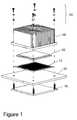
- FIG. 1is a cross-sectional view of an integrated circuit assembly incorporating an LGA connector according to one embodiment of the present invention.
- FIG. 2Ais a cross-sectional view of a connector according to one embodiment of the present invention.
- FIG. 2Bis a top view of a contact element in the connector of FIG. 2A.
- FIG. 2Cis a top view of a contact element according to another embodiment of the present invention.
- FIG. 3is a cross-sectional diagram illustrating the use of a connector for interconnecting a land grid array package and a PC board in accordance with the present invention.
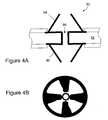
- FIG. 4Ais a cross-sectional view of a connector according to one embodiment of the present invention.
- FIG. 4Bis a top view of a contact element in the connector of FIG. 4A.
- FIG. 4Cis a perspective view of a connector according to one embodiment of the present invention.
- FIG. 5Ais a cross-sectional view of a connector according to an alternate embodiment of the present invention.
- FIG. 5Bis a top view of a contact element in the connector of FIG. 5A.
- FIG. 6is a cross-sectional view of a connector according to one embodiment of the present invention.
- FIGS. 7A to 7 Care cross-sectional views of the connector of FIG. 6 being applied in a hot-swapping operation.
- FIG. 7Dillustrates the optimization of the contact force using two contact elements with different spring constants.
- FIG. 7Eillustrates a connector including contact elements formed using multiple layers of metals according to another embodiment of the present invention.
- FIG. 8A and 8Bare cross-section view of connectors including ground planes for improving signal integrity and for controlling contact element impedance.
- FIG. 9Aillustrates one embodiment of a circuitized connector in accordance with the present invention.
- FIG. 9Billustrates another embodiment of a circuitized connector according to the present invention.
- FIG. 10Aillustrates another embodiment of a circuitized connector in accordance with the present invention.
- FIG. 10Bis a top view of the electrical circuit formed in the dielectric substrate of the connector of FIG. 10A.
- FIG. 10Cillustrates another embodiment of a circuitized connector in accordance with the present invention.
- FIG. 10Dis a top view of the electrical circuit formed in the dielectric substrate of the connector of FIG. 10C.
- FIG. 11illustrates a connector incorporating thermally conductive planes according to one embodiment of the present invention.
- FIG. 12illustrates the operation of the thermally conductive planes in the connector of FIG. 11.
- FIG. 13Ais a cross-sectional view of a connector including a coaxial contact element according to one embodiment of the present invention.
- FIG. 13Bis a top view of the coaxial contact elements of FIG. 13A.
- FIG. 14illustrates the mating of an LGA package to a PC board through the connector of FIG. 13A.
- FIG. 15is a cross-sectional view of a printed circuit board incorporating a contact grid array according to one embodiment of the present invention.
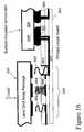
- FIG. 16is a cross-sectional view of a printed circuit board incorporating a contact grid array according to another embodiment of the present invention.
- a connector for a land grid array (LGA) package or area arrayincludes an array of contact elements formed on a dielectric substrate where each contact element includes an elastic portion having an elastic working range on the order of the electrical path length of the contact element.
- the large elastic working range of the LGA connector of the present inventionallows the connector to accommodate coplanarity deviations or positional misalignment that may be present in most electronic components to be connected, thereby providing high quality and reliable electrical connection between electronic components.
- the connector of the present inventionprovides separable or remountable connection and is capable of retaining high quality electrical connection over repeated insertions.
- the contact elementis formed as metal flanges extending from a ring-shaped base.
- the connector of the present inventionprovides numerous advantages over conventional systems.
- the connector of the present inventionis scalable in both pitch and height to less than 1 mm and is therefore suitable for use with electronic components packaged with small lead geometries and large lead count packages.
- the connector of the present inventionis capable of accommodating normal variations in coplanarity and positional misalignment of the electronic component to be connected while still meeting the mechanical, electrical, and reliability requirements of connectors for use with small lead geometries and large lead count electronic components.
- the contact elements of the connector of the present inventionare capable of maintaining elasticity over a range that accommodates positional tolerances in most applications, even for lead pitches of 1 mm or less.
- the connector of the present inventionis capable of providing a mechanical working range of more than 200 microns with an insertion force of 40 grams or less per contact.
- the connector of the present inventioncan accommodate coplanarity variations and positional misalignments on the order of 200 microns or more while maintaining a relatively low insertion force (40 grams or less per contact).
- Conventional connector technologiesthus far have not been able to accommodate coplanarity variations while still provide satisfactory mechanical or electrical or reliability properties.
- the connector of the present inventionis capable of achieving good signal integrity at frequencies above 1 GHz. Furthermore, the connector can meet high frequency performance requirement even when the spacing between contact elements is on the order of 1 mm or less.
- the connector of the present inventioncan be adapted for a wide variety of applications.
- the connectorcan be used to connect an LGA package to a PC board.
- the connectorcan also be used to connect between LGA area arrays on two PC boards.
- the connector of the present inventioncan be used to connect to LGA pads formed on any electronic components, such as on an LGA package, on a multi-chip module or on a PC board.
- the connector of the present inventioncan be formed by providing contact elements on one side of the connector only.
- the other side of the connectorcan be formed by providing pins, solder balls or other conventional connection mechanism.
- the connector of the present inventioncan also be formed by providing contact elements on both side of the connector so that the connector can be used to mate two LGA packages together or provide separable connection of an LGA package to pads on a PC board.
- an electrical interconnect or a connectorrefers to a device for connecting two electronic components together, such as an IC chip to a PC board, or for connecting an electronic component to an equipment, such as a tester.
- the term “electrical interconnect” or “electrical connector”will be used interchangeably to refer to the connector of the present invention for connecting to an electronic component using LGA pads for leads.
- An electrical interconnect system or an electrical connector, as described herein,can be used for electrically connecting two or more electronic components together or for electrically connecting an electronic component to a piece of equipment.
- the electronic componentscan include integrated circuit (IC) or chips, printed circuit boards or multi-chip modules.
- the LGAis sometimes referred to as an area array.
- the equipmentcan include test equipment such as an electrical tester.
- the term “lead”will be used collectively to refer to the electrical connections on the electronic components for making electrical contact with circuitry on or within the electronic components.
- the leads of an electronic componentcan include, but are not limited to, the pads of a land-grid array package or the pads on a printed circuit board.
- the connector of the present inventionis sometimes referred to as an LGA connector, it is understood that the connector of the present invention can be used with any electronic components including pads or “lands” as the electrical connection.
- LGA connectoris illustrative only and is not intended to limit the present invention to be used with LGA packages only.
- FIG. 1is a cross-sectional view of an integrated circuit assembly incorporating an LGA connector according to one embodiment of the present invention.
- FIG. 1illustrates one application in which the LGA connector of the present invention can be advantageously applied.
- an LGA connector 12is used to connect an LGA package 10 to a PC board 14 .
- the integrated circuit assemblycan be secured by a bolster plate 16 and hardware 20 which provide compressive force between the LGA package and the PC board.
- a heat sink 18is sometimes included and placed on the top of LGA package 10 to provide heat dissipation for the integrated circuit chip in the LGA package.
- FIG. 2Ais a cross-sectional view of a connector according to one embodiment of the present invention.
- FIG. 2Bis a top view of a contact element in the connector of FIG. 2A.
- connector 50includes a substrate 52 made of a dielectric material.
- the substrateis a dielectric layer made of FR- 4 or polyimide.
- connector 50is shown with a single contact element 54 built on the top surface of substrate 52 .
- connector 50will include multiple number of contact elements 54 arrayed on the top surface of the substrate. The number and arrangement of contact elements are selected based on the electronic component to which the connector is to be connected.
- Contact element 54is formed using a conductive metal and includes a base portion 55 A and one or more elastic portions 55 B.
- base portion 55 Ais formed in a the shape of a ring (FIG. 2B) and elastic portions 55 B are formed as flanges extending inwardly from base portion 55 A.
- elastic portions 55 Bare formed protruding above base portion 55 A and substrate 52 .
- elastic portions 55 Bare compressed against a pad of an electronic component to be connected to provide electrical connection to the electronic component.
- base portion 55 A of contact element 54is formed on the top surface of substrate 52 and embedded underneath a dielectric layer. In other embodiments, base portion 55 A can be formed directly on the top surface of substrate 52 as well.
- Contact element 54is formed using a conductive metal that can provide the desired elasticity.
- contact element 54can be formed using a copper-alloy (Cu-alloy) or a multilayer metal sheet such as stainless steel coated with Copper-Nickel-Gold (Cu/Ni/Au) multilayer metal sheet.
- the contact elementsare formed using a small-grained copper-beryllium (CuBe) alloy.
- each contact element 54is coupled to a corresponding terminal 58 on the bottom surface of substrate 52 .
- a via 56is formed in substrate 52 and includes a conductive line electrically connecting contact element 54 and terminal 58 .
- via 56is formed adjacent contact element 54 and is connected to base portion 55 A of the contact element as shown in FIG. 2B.
- Terminal 58can be formed as any type of electrical connection.
- terminal 58is formed as a solder ball.
- Connector 50thus can be used as an interconnect between an LGA package and a PC board where the solder ball of terminal 58 can be bonded to a pad on the PC board.
- Terminal 58can also be formed as pins or other contact structure, currently available or to be developed.
- terminal 58 and via 56are not critical to the practice of the present invention. According to an alternate embodiment of the present invention to be described in more detail below, terminal 58 can be formed using a second set of contact elements 54 so that the connector thus formed can be used to separably connect between pads of two LGA electronic components.
- terminal 58is shown as being formed in vertical alignment with contact element 54 .
- This configurationis illustrative only and terminal 58 may be formed in any position relative to contact element 54 depending on the application.
- terminal 58may be formed in an offset position from contact element 54 .
- the exact location or placement of terminal 58 relative to contact element 54is not critical to the connector of the present invention.
- contact element 54is formed as including a ring-shaped base portion and four elastic portions.
- the contact elementis coupled to terminal 58 through via 56 .
- the base portionis formed as a contiguous ring connecting the four elastic portions to via 56 .
- This configurationis illustrative only and is not intended to be limiting.
- the contact element of the present inventioncan be formed in a variety of configurations and each contact element only needs to have a base portion sufficient for attaching the elastic portion to the dielectric substrate.
- the base portioncan assume any shape and does not have to be in the form of a closed circle.
- a contact elementincludes a base portion 59 A and an elastic portion 59 B extending from the base portion.
- a viacan be formed in the base portion of the contact element for connecting the contact element to the respective terminal on the other side of the dielectric substrate.
- a contact elementcan include multiple separate base and elastic portions as shown in FIG. 2C. Although each of the base and elastic portions in the contact element are isolated from each other, they can be connected by metal traces in the dielectric substrate so that all base and elastic portions associated with one contact element are connected to a single terminal.
- the elastic portion of the contact elementhas a large elastic working range so that the elastic portion operates entirely in the elastic regime when compressed. Specifically, in one embodiment, the elastic portion behaves elasticity over substantially the entire electrical path length of the contact element.
- the “electrical path length” of the contact elementis defined as the distance the electrical current has to travel from the pad of the electronic component to the connector and is illustrated as the distance A-A′ in FIG. 2A.
- elastic portion 55 Bremains elastic over the entire electrical path length and does not become plastically deformed under typical load condition or typical insertion force that is applied to the connector when used in an integrated circuit assembly.
- the elastic working range of the elastic portionis maintained even when the dimension of the contact element is scaled down. This represent a significant improvement over conventional interconnect technologies which can become plastically deformed at a lower contact force when the contacts are scaled down.
- the conventional interconnect technologiescannot provide reliable separable connections because the connectors typically become permanently deformed upon initial insertion.
- the connector of the present inventioncan provide reliable remountable connection even over repeated insertions.
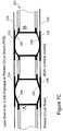
- FIG. 3is a cross-sectional diagram illustrating the use of a connector 60 for interconnecting a land grid array package 62 and a PC board 64 .
- connector 60includes a first set of contact elements formed on the top surface of the connector and a second set of contact elements formed on the bottom surface of the connector.
- connector 60 of the present inventionprovides reliable electrical connection between LGA package 62 and PC board 64 , despite the presence of coplanarity variations.
- some contact elementssuch as 66 A and 66 B
- other contact elementssuch as 68 A and 68 B
- the large elastic working range of the contact elementsalso permit the contact elements to make contact to pads that are positionally misaligned (such as pad 69 on PC board 64 ).
- each pad on LGA package 62is connected to each pad of PC board 64 through a pair of contact elements in connector 60 . Either LGA package 62 or PC board 64 can be demounted and remounted without degrading the integrity of connector 60 .
- contact element 54is formed on a contiguous substrate 52 .
- substrate 52may include apertures or holes, such as those for use in through-hole connection of conductive elements on the two surfaces of the substrate.
- FIG. 4Ais a cross-sectional view of a connector according to an alternate embodiment of the present invention.
- FIG. 4Bis a top view of a contact element in the connector of FIG. 4A.
- connector 80includes two sets of contact elements formed on the top and bottom surfaces of dielectric substrate 82 .
- connector 80can be used to connect between two land grid array components with pads as leads.
- connector 80includes a central aperture 88 formed in dielectric substrate 82 .
- Conductive traces for connecting contact element 84 on the top surface to contact element 86 on the bottom surfaceare coupled through central aperture 88 .
- the diameter of central aperture 88can be varied and can be made as large as the base portion of the contact elements. The exact dimension of central aperture 88 is not critical to the practice of the present invention.
- FIG. 4Aillustrates connector 80 as including one contact element 84 connected to one contact element 86 .
- connector 80typically includes an array of contact elements arranged in a manner to meet the floor plan of the leads of the electronic modules to be connected.
- FIG. 4Cis a perspective view of a connector 80 according to one embodiment of the present invention.
- connector 100includes a first set of contact elements 104 formed on a first major surface of a dielectric substrate 102 and a second set of contact elements 106 formed on a second major surface of dielectric substrate 102 .
- Each pair of contact elements 104 and 106are aligned with a hole 108 formed in substrate 102 .
- Metal tracesare formed through hole 108 to connect a contact element from the first major surface to a contact element from the second major surface.
- FIG. 4Cillustrates connector 100 during an intermediate step in the manufacturing process for forming the connector. Therefore, the array of contact elements is shown as being connected together on a sheet of metal or metallic material. In the subsequent manufacturing steps, the metal sheet between the contact elements are patterned to remove unwanted portions of the metal sheet so that the contact elements are isolated as needed. For example, the metal sheet can be etched to isolate each contact element.
- the process for forming the connector of the present inventionwill be described in more detail below.
- the connector of the present inventionis formed as follows. First, a dielectric substrate including conductive paths between the top surface and the bottom surface is provided. The conductive paths can be in the form of vias or an aperture as shown in FIG. 2A and FIG. 4A. In one embodiment, the dielectric substrate is a piece of FR- 4 material with plated through holes. A conductive metal sheet or a multi-layer metal sheet is then patterned to form an array of contact elements including the base portion and the elastic portion(s). The contact elements can be formed by etching or stamping or other means. The protrusion or bending of the elastic portions of the contact elements can be formed by stamping. The metal sheet is attached to the first major surface of the dielectric substrate.
- a second conductive metal sheet or multi-layer metal sheetis accordingly patterned and attached to the second major surface of dielectric substrate 102 .
- the metal sheet(s)can then be patterned to remove unwanted metal from the sheet(s). For example, the metal sheet(s) may be etched so that the contact elements are isolated from each other as needed.
- the metal sheet(s)can be patterned by etching or scribing or stamping or other means.
- the connector of the present inventioncan be manufactured in a variety of processes and in a variety of process sequences.
- the above-described processis illustrative only and is not intended to be limiting.
- the protrusion of the elastic portionscan be formed after the metal sheet including patterned contact elements has been attached to the dielectric substrate.
- the unwanted portions of the metal sheet(s)can be removed before the contact elements are formed.
- the unwanted portions of the metal sheet(s)can be removed before the metal sheet(s) are attached to the dielectric substrate.
- conductive tracesare formed in the plated through holes and also on the surface of the dielectric substrate 102 in a ring-shaped pattern encircling each plated through holes (denoted as feature 103 ). While such a conductive ring can be provided to enhance the electrical connection between the contact elements on the metal sheet and the conductive traces formed in the dielectric layer, the conductive ring is not a required component of the connector of the present invention.
- the connectorcan be formed by using a dielectric substrate including through holes (not plated). A metal sheet including an array of contact elements can be attached to the dielectric substrate.
- the entire structurecan then be plated to form conductive traces in the through holes connecting the contact elements through the holes to the respective terminals on the other side of the dielectric substrate.
- the dimension, geometry and material composition of the elastic portion of the contact elementcan be varied to provide the desired mechanical and electrical properties.
- the thickness, width, length, and shape of the elastic portionscan be selected to provide the desired elasticity.
- the number of elastic portionscan also be selected to obtain the desired mechanical and electrical properties. The description below provides more details concerning the relationship between the size and geometry of the elastic portions and the electrical and mechanical properties of the same.
- FIGS. 5A and 5Billustrate a contact element according to an alternate embodiment of the present invention.
- a connector 150 in accordance with the present inventionincludes a contact element 154 formed on a dielectric substrate 152 .
- Contact element 154includes a base portion 156 and two elastic portions 158 and 160 extending from the base portion.
- elastic portions 158 and 160are formed in a spiral shape whereby the two elastic portions extend upward from the top surface of substrate 152 in spiral fashion.
- the spiral shaped elastic portionsprovide additional benefits over a linearly shaped elastic portions. Specifically, the length of the elastic portions engaging a land area is effectively extended and the elastic working range of the elastic portion is accordingly lengthened.
- the elastic portionscan be formed in a variety of shapes to obtain the desired mechanical and electrical properties.
- a connector for land grid array(an LGA connector) is provided with contact elements with different operating properties. That is, the LGA connector includes heterogeneous contact elements where the operating properties of the contact elements can be selected to meet requirements in the desired application.
- the operating properties of a contact elementrefer to the electrical, mechanical and reliability properties of the contact element.
- individual contact elements of the LGA connectorcan be formed using any conventional LGA interconnect technology.
- a contact elementincludes a conductive portion for engaging the pad of the land grid array.
- Individual contact elementscan be formed on the top surface of the dielectric substrate, such as by placing the contact elements directly on the top surface, or by embedding a portion of the contact element within the top surface, or by forming a portion of the contact element within an aperture on the top surface of the dielectric substrate.
- contact elements in the form of metal springs, bundled wires, metal in polymer, solid metal tabs, or any other electrical contact technologycan be used to form the individual contact elements.
- an LGA connector including heterogeneous contact elementsis formed by incorporating different types of contact elements, each contact element selected to provide the desired operating properties.
- the LGA connectormay include one or a group of contact elements formed using metal springs, one or a group of contact elements formed using bundle wires, and one or a group of contact elements formed using the contact element of FIG. 2A or 4 A.
- an LGA connector including heterogeneous contact elementsis formed by using one type of contact elements (such as the contact element of FIG. 2A or 4 A) and specifically engineering one or a group of contact elements to provide a desired operating property different than the operating property of the remaining contact elements.
- an LGA connectorincludes a first set of contact elements requiring a low contact force and a second set of contact elements requiring a large contact force to engage.
- a larger contact forcecorrelates to a more robust and lower resistance electrical contact.
- contact elements to be connected to the power and ground pins of an integrated circuitare formed as contact elements requiring a large contact force while contact elements to be connected to the signal pins of the integrated circuit are formed as contact element requiring a low contact force.
- the power and ground pins carrying high currentcan have a low resistance electrical path to minimizing Joule heating while the signal pins can have low contact force to minimize the overall contact force required for the connector.
- the following mechanical propertiescan be specifically engineered for a contact element or a set of contact elements to achieve certain desired operational characteristics.
- the contact force for each contact elementcan be selected to ensure either a low resistance connection for some contact elements or a low overall contact force for the connector.
- the elastic working range of each contact element over which the contact element operates as required electricallycan be varied between contact elements.
- the vertical height of each contact elementcan be varied, such as for accommodating coplanarity variations.
- the pitch or horizontal dimensions of the contact elementcan be varied.
- the electrical propertiescan be specifically engineered for a contact element or a set of contact elements to achieve certain desired operational characteristics.
- the DC resistance, the impedance, the inductance and the current carrying capacity of each contact elementcan be varied between contact elements.
- a group of contact elementscan be engineered to have lower resistance or a group of contact elements can be engineered to have low inductance.
- the contact elementscan be engineered to obtain the desired reliability properties for a contact element or a set of contact elements to achieve certain desired operational characteristics.
- the contact elementscan be engineered to display no or minimal performance degradation after environmental stresses such as thermal cycling, thermal shock and vibration, corrosion testing, and humidity testing.
- the contact elementscan also be engineering to meet other reliability requirements defined by industry standards, such as those defined by the Electronics Industry Alliance (EIA).
- the mechanical and electrical properties of the contact elementscan be modified by changing the following design parameters.
- the thickness of the elastic portionsuch as the flanges, can be selected to give a desired contact force.
- a flange thickness of about 40 micronstypically gives low contact force on the order of 20 grams or less while a flange thickness of 80 microns gives a much higher contact force of over 100 grams for the same displacement.
- the width, length and shape of the elastic portioncan also be selected to give the desired contact force.
- the number of elastic portions to include in a contact membercan be selected to achieve the desired contact force, the desired current carrying capacity and the desired contact resistance. For example, doubling the number of flanges roughly doubles the contact force and current carrying capacity while roughly decreasing the contact resistance by a factor of two.
- specific metal composition and treatmentcan be selected to obtain the desired elastic and conductivity characteristics.
- Cu-alloyssuch as copper-beryllium
- metal multi-layerscan be used to provide both excellent mechanical and electrical properties.
- a stainless steel flangeis coated with copper (Cu) and then nickel (Ni) and finally gold (Au) to form a stainless steel/Cu/Ni/Au multilayer.
- the stainless steelwill provide excellent elasticity and high mechanical durability while the Cu provides excellent conductivity and the Ni and Au layers provide excellent corrosion resistance.
- cold working, alloying, annealing, and other metallurgical techniquescan be used to engineer the specific desired properties of the elastic portion.
- FIG. 6is a cross-sectional view of a connector according to one embodiment of the present invention.
- connector 200includes a first contact element 204 and a second contact element 206 formed on the top surface of a dielectric substrate 202 .
- a matching pair of contact elements 207 and 208is also formed on the bottom surface of dielectric substrate 202 to be connected to contact elements 204 and 206 , respectively.
- contact elements 207 and 208are optional and the bottom terminals of connector 200 may include other types of connection, such as a solder ball or a pin.
- contact element 204includes four elastic portions formed as flanges projecting straight or linearly from the base portion.
- contact element 206includes three elastic portions formed as flanges extending from the base portion in a concave curvature.
- the width of the flanges in contact element 204is larger than the width of the flanges in contact element 206 .
- the height of the elastic portions of contact element 206is greater than the height of the elastic portions of contact element 204 .
- contact element 204requires a larger contact force than contact element 206 .
- contact element 204has lower contact resistance and higher current carrying capacity.
- the LGA connector of the present inventioncan be advantageously applied in “hot-swapping” applications.
- Hot-swappingrefers to mounting or demounting an electronic component while the system to which the component is to be connected is electrically active without damaging to the electronic component or the system.
- various power and ground pins and signal pinsmust be connected and disconnected in sequence and not at the same time in order to avoid damages to the component or the system.
- taller contact elementscan be use to make electrical connection before shorter contact elements. In this manner, a desired sequence of electrical connection can be made to enable hot-swapping operation.
- FIGS. 7A to 7 Care cross-sectional views of connector 200 of FIG. 6 being applied in a hot-swapping operation.
- the height of contact elements 206 and 208are selected to obtain the desired contact force and desired spacing to achieve reliable hot-swapping operation.
- connector 200is shown in the unloaded condition.
- Connector 200is to be connected to a land grid array (LGA) package 220 and a printed circuit board (PC board) 222 .
- a pad 230 on LGA package 220represents a power connection (that is, either the positive power supply voltage or the ground voltage) of the integrated circuit packaged in the LGA package which is to be connected to a pad 232 on PC board 222 .
- Pad 232 on PC board 222is electrically active or “powered-up”.
- a pad 234 on LGA package 220represents a signal pin of the integrated circuit which is to be connected to a pad 236 on PC board 222 .
- connector 200includes contact elements 206 and 208 having an extended height and a larger elastic working range than contact elements 204 and 207 such that hot-swapping operation between LGA package 220 and PC board 222 is realized using connector 200 .
- FIG. 7Billustrates an intermediate step during the mounting process of LGA package 220 to PC board 222 using connector 200 .
- pad 230 and pad 232will make electrical contacts to respective contact elements 206 and 208 prior to pads 234 and 236 making connection to contact elements 204 and 207 .
- the power connection between LGA package 220 and PC board 222is established before the signal pads are connected.
- FIG. 7Cillustrates the mounting of LGA package 220 to PC board 222 in a fully loaded condition.
- LGA package 220is compressed against connector 200 so that contact element 204 engages signal pad 234 .
- PC board 222is compressed against connector 200 so that contact element 207 engages pad 236 on the PC board.
- the LGA packageis thus mounted onto PC board.
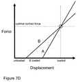
- the taller contact elements 206 , 208are compressed more to allow the shorter contact elements 204 and 207 to engage, the contact force required for the connector will increase.
- the taller contact elements 206 , 208can be designed with a lower spring constant than the shorter contact elements 204 and 207 such that all contact elements are at the optimal contact force in the fully loaded condition.
- FIG. 7Dillustrates the optimization of the contact force using two contact elements with different spring constants.
- there is generally an optimal contact forcewhich is the minimum contact force that needs to be applied to provide a stable, reliable electrical connection.
- both contact elementscan be at their respective optimal contact force when an electronic component is fully loaded onto the connector.
- contact element 206can be made to behave according to curve B having a less stiff or more elastic characteristic.
- contact element 206can withstand a larger displacement before reaching its optimal contact force.
- contact element 204can be made to behave according to curve A having a more stiff or less elastic characteristic.
- contact element 204withstands a lesser amount of displacement before reaching its optimal contact force.
- both contact element 206 and contact element 204are at the optimal contact force.
- FIGS. 6 and 7A to 7 Cillustrate one embodiment of the connector of the present invention where the contact elements are given different mechanical properties to enable the use of the connector for hot-swapping operation.
- the connector of the present inventioncan be designed to include contact elements of other differing mechanical and electrical properties depending on the application in which the connector is used.
- the differing mechanical and electrical properties of the contact elementscan be obtained by forming the contact elements using different sheets of metal formed on different layers.
- contact elements 204 and 206are formed using two different metal layers. Specifically, contact element 204 is formed using metal layer 244 while contact element 206 is formed using metal layer 246 .
- Metal layers 244 and 246are patterned so that only specific contact element or a specific group of contact elements is formed using the respective metal layer. Accordingly, contact element 204 is formed using a different metal alloy than contact element 206 .
- the elasticity or current carrying capability of the individual contact elementcan be tailored to obtain the desired mechanical, electrical and reliability properties.
- FIG. 7Eillustrates a connector including contact elements formed using multiple layers of metals according to another embodiment of the present invention.
- connector 250includes a multi-layer structure for forming a first group of contact elements 252 and a second group of contact elements 254 .
- the first group of contact elements 252is formed using a first metal layer 256
- the second group of contact elements 254is formed using a second metal layer 260 .
- First metal layer 256 and second metal layer 260are isolated by a dielectric layer 258 .
- Each metal layeris patterned so that a group of contact elements are formed at desired locations on the specific metal layer. For instance, referring to FIG.
- contact elements 252 formed using first metal layer 256constitute ground pin connections whereby the contact elements are connected together using a ground plane formed in substrate 262 .
- contact elements 254 formed by second metal layer 260constitute individual signal pin connections which are isolated from the ground pin connections in the first metal layer.
- connector 250can be formed using the following process sequence.
- First metal layer 256is stamped to form the first group of contact elements.
- the stamped metal layer 256can then be attached to dielectric substrate 262 .
- an insulating layer, such as dielectric layer 258is formed over first metal layer 256 .
- a second stamped metal layer 260can be stamped and attached to the dielectric layer 258 .
- Via holes and conductive tracesare formed in dielectric substrate 262 and in dielectric layer 258 as needed to provide a conductive path between each contact element to a respective terminal on the opposing side of substrate 262 .
- a multi-layer metal structureis formed whereby each metal layer is insulated from the other and different groups of contact elements can be formed using the different metal layers.
- the different metal layersmay include metal layers with different thicknesses or different metallurgies.
- FIGS. 6 and 7A to 7 Eillustrate an LGA connector formed using the contact elements of the present invention
- an LGA connector including heterogeneous contact elementscan be formed using other types of contact elements.
- the use of the contact elements of the present inventionis illustrative only and is not intended to limit the connector of the present invention to include contact elements of the present invention and described above.
- a connectoris provided with ground planes and the impedance of the contact elements can be controlled by varying the distance between the contact element for a signal pin and the ground plane or between the contact element for a signal pin and the contact element for a ground pin.
- FIGS. 8A and 8Bare cross-section view of connectors including ground planes for improving signal integrity and for controlling contact element impedance.
- a connector 300includes a contact element 302 which is to be connected to a signal pin on an electronic component.
- Connector 300further includes contact elements 304 and 306 which are to be connected to the ground potential of the electronic component.
- Connector 300includes ground planes 310 which are formed on and in dielectric substrate 320 .
- Ground planes 310can formed on the top surface of substrate 320 or embedded in substrate 320 .
- ground planes 310are connected to contact elements 304 and 306 to be electrically coupled to the ground potential.
- ground planes 310can be coupled to the ground potential through other means.
- ground planes 310in connector 300 has the effect of improving the signal integrity of the AC electrical signals that are connected through connector 300 .
- connector 300includes ground planes 310 which function to reduce noise and improve signal integrity of the connector.
- the distance B to B′ between the metal planes associated with contact element 302 for a signal pin and the metal planes associated with contact elements 304 and 306 for the ground potentialcan be varied to obtain a desired impedance for contact element 302 .
- FIG. 8Billustrates another embodiment of the connector of the present invention where a pair of contact elements 352 and 354 are used to couple to a pair of differential signals.
- contact elements 352 and 354are each formed as including conductive planes (such as conductive plane 360 ).
- the impedance of contact elements 352 and 354can be adjusted by varying the distance between the conductive planes associated with the contact elements.
- an LGA connectoris circuitized to incorporate an electrical circuit connecting to one or more contact elements of the connector.
- the electrical circuitincludes surface mounted or embedded electrical components.
- the LGA connector of the present inventioncan be provided with improved functionality.
- a circuitized connector of the present inventioncan be formed using any conventional LGA interconnect technology.
- the connectorcan include contact elements in the form of metal springs, bundled wires, metal in polymer, solid metal tabs, or any other electrical contact technology.
- a contact elementincludes a conductive portion for engaging the pad of the land grid array.
- the LGA connectorcan be formed using the contact element of the present invention and described above.
- Individual contact elementscan be formed on the top surface of the dielectric substrate, such as by placing the contact elements directly on the top surface, or by embedding a portion of the contact element within the top surface, or by forming a portion of the contact element within an aperture on the top surface of the dielectric substrate.
- FIG. 9Aillustrates one embodiment of a circuitized connector in accordance with the present invention.
- connector 400includes a contact element 404 on the top surface of dielectric substrate 402 connected to a contact element 406 on the bottom surface of dielectric substrate 402 .
- contact element 404is connected to a surface mounted electrical component 410 and an embedded electrical component 412 .
- Electrical components 410 and 412may be decoupling capacitors which are positioned on connector 400 so that the capacitors can be placed as close to the electronic component as possible. In conventional integrated circuit assembly, such decoupling capacitors are usually placed on the printed circuit board, distant from the electronic component.
- circuitized connector 400By using circuitized connector 400 , the decoupling capacitors can be placed as close to the electronic component as possible to enhance the effectiveness of the decoupling capacitors.
- Other electrical componentsthat may be used to circuitize the connector of the present invention include a resistor, an inductor and other passive or active electrical components.
- FIG. 9Billustrates another embodiment of a circuitized connector according to the present invention.
- Connector 500include a contact element 504 on a dielectric substrate 502 coupled to a solder ball terminal 506 through a via 508 .
- Contact element 504is connected to a surface mounted electrical component 510 and to an embedded electrical component 512 .
- Connector 500further illustrates that the placement of terminal 506 does not have to be aligned with contact element 504 as long as the contact element is electrically coupled to the terminal, such as through via 508 .
- a connector of the present inventionis circuitized by linking or connecting the power supply pins of the electronic components together, as illustrated in FIGS. 10A and 10B.
- a connector 550includes a contact element 552 and a contact element 554 for carrying signals and contact elements 556 A to 556 C for coupling to a power supply potential, such as a Vcc or a ground potential.
- connector 550is circuitized by including a conductive plane 558 electrically connecting contact elements 556 A to 556 C together.
- conductive plane 558is forming embedded in substrate 560 and is patterned so that the plane is electrically isolated from contact elements 552 and 554 (FIG. 10B). As demonstrated in FIG. 8, if the conductive plane 558 is a ground plane, the gaps between the conductive plane 558 and the contact elements 552 and 554 can be used to control the contact impedances of contact elements 552 and 554 .
- a circuitized connectorincludes an electrical circuit to redistribute one or more signals from one lead of the electronic component to a number of leads of the other electronic component connected to the connector.
- FIGS. 10C and 10Dillustrate a circuitized connector according to an alternate embodiment of the present invention.
- a circuitized connector 570includes contact elements 572 , 574 , 576 , 578 and 580 . Instead of being connected to a terminal in vertical alignment to each contact element, connector 570 is circuitized so that a contact element formed on the top surface of the substrate may be connected to any one or more terminals formed on the bottom of the substrate.
- the interconnection between the contact elements and the terminalscan be realized using metal traces formed in an intermediate layer embedded within the connector substrate.
- contact element 572is connected to a terminal 582 directly below.
- contact element 574is routed by metal trace 592 to be connected to terminal 588 .
- contact element 578is routed by metal trace 594 to be connected to terminal 584 .
- contact element 576is connected to terminal 586 but also connected to contact element 580 and terminal 590 through metal trace 596 .
- a connector of the present inventioncan be circuitized to connect one contact element to a terminal positioned anywhere on the opposite surface of the dielectric substrate.
- the connector of the present inventioncan be used to connect a contact element to a plural number of terminals so that any signal applied to the one contact element can be distributed to the plural number of terminals.
- FIGS. 9A, 9B, 10 A and 10 Cillustrate circuitized connectors formed using the contact elements of the present invention
- a circuitized LGA connectorcan be formed using other types of contact elements.
- the use of the contact elements of the present inventionis illustrative only and is not intended to limit the connector of the present invention to include only contact elements of the present invention and described above.
- an LGA connectorincorporates embedded thermal dissipation structures to provide enhanced heat dissipation capability at specific contact elements. For instance, when a contact element engaging a lead of an electronic package carries more than 1 A of current, significant Joule heating can result creating a temperature rise of 20 degrees or more at the contact element.
- an LGA connectorincludes embedded thermal dissipation structures so as to effectively limit the temperature rise at specific contact elements. For example, the amount of temperature rise can be reduced to 10 degrees or less by the use of the embedded thermal dissipation structures in the connector of the present invention.
- FIG. 11illustrates a connector incorporating thermally conductive planes according to one embodiment of the present invention.
- connector 600includes contact elements 604 and 606 formed on the top surface of dielectric substrate 602 .
- Thermally conductive planes 620 and 622are formed in substrate 602 during the manufacturing process of substrate 602 .
- Thermally conductive planes 620 and 622provide heat dissipation function for contact elements 604 , 608 , 606 and 607 .
- the thermally conductive planesare formed using Cu.
- the thermally conductive planesare formed using filled epoxy, which is not electrically conductive and be in intimate contact with the vias or contact elements without shorting the electrical paths.
- FIG. 12illustrates the operation of the thermally conductive planes in connector 600 .
- contact elements 606 and 607are to be connected to pads of the LGA package and the PC board representing a high current connection.
- Joule heating at the padsoccurs causing heat to be generated at the pads of the LGA package and the PC board.
- Thermally conductive planes 620 and 622function to dissipate the heat away from contact elements 606 and 607 .
- the neighboring contact elements 604 and 608are connected to a low current carrying signal.
- heat generated at contact elements 606 and 607can be dissipated through thermally conductive planes 620 and 622 and through contact elements 604 and 608 .
- a LGA connector incorporating thermal dissipation structurecan be formed using other types of contact elements.
- the connectorcan be formed using metal springs and bundle wires.
- the use of the contact elements of the present invention in the LGA connector of FIG. 11is illustrative only and is not intended to limit the connector of the present invention to include only contact elements of the present invention and described above.
- a connectorincludes one or more coaxial contact elements.
- FIG. 13Ais a cross-sectional view of a connector including a coaxial contact element according to one embodiment of the present invention.
- FIG. 13Bis a top view of the coaxial contact elements of FIG. 13A.
- connector 700includes a first contact element 704 and a second contact element 706 formed on the top surface of a dielectric substrate.
- Contact elements 704 and 706are formed in proximity to but electrical isolated from each other.
- contact element 704includes a base portion formed as an outer ring of aperture 703 while contact element 706 includes a base portion formed as an inner ring of aperture 703 .
- Each of contact elements 704 and 706includes three elastic portions (FIG. 13B). The elastic portions of contact element 704 do not overlap with the elastic portions of contact element 706 .
- contact element 704is connected to a contact element 708 on the bottom surface of dielectric substrate 702 through a via 712 .
- Contact elements 704 and 708form a first current path, referred herein as the outer current path of connector 700 .
- contact element 706is connected to a contact element 709 on the bottom surface of dielectric substrate 702 through a metal trace formed in aperture 703 .
- Contact elements 706 and 709form a second current path, referred herein as the inner current path of connector 700 .
- connector 700can be used to interconnect a coaxial connection on a LGA package 730 to a coaxial connection on a PC board 732 .
- FIG. 14illustrates the mating of LGA package 730 to PC board 732 through connector 700 .
- contact element 704engages a pad 742 on LGA package 730 .
- contact element 708engages a pad 746 on PC board 732 .
- the outer current path between pad 742 and pad 746is formed.
- the outer current pathconstitutes a ground potential connection.
- contact element 706engages a pad 744 on LGA package 730 while contact element 709 engages a pad 748 on PC board 732 .
- the inner current path between pad 744 and pad 748is formed.
- the inner current pathconstitutes a high frequency signal.
- a particular advantage of the connector of the present inventionis that the coaxial contact elements can be scaled to dimensions of 1 mm or less.
- the connector of the present inventioncan be used to provide coaxial connection even for small geometry electronic components.
- the connector of the present inventionis illustrated as being used to interconnect an LGA package to a PC board.
- the connectorcan be used to interconnect two PC boards or two chip modules together.
- the connector of the present inventioncan be generally applied to connect the metal pads (lands) of an area array on an electronic component to the metal pads (lands) of an area array on another electronic component.
- the connector of the present inventionprovides particular advantages as PC boards are almost never coplanar.
- the connector of the present inventioncan be applied to accommodate a large coplanarity variation, such as on the order of 200 microns or more, with an insertion force of about 40 grams per contact or less, the connector of the present invention can be readily applied to make area array connections between two PC boards. Furthermore, the connector of the present invention is scalable in both pitch and height to less than 1 mm and is therefore suitable for use in small dimensional area array connections.
- various embodiments of the connectorare illustrated as including a first contact element on top and a second contact element on the bottom surface of the substrate.
- a second contact element on the bottom surface of the substrateto serve as a terminal for the first contact element is illustrative only.
- the terminalcan be formed as other types of electrical connection such as a solder ball or a pin.
- a printed circuit boardincorporates an area array of LGA contact elements.
- an LGA package, an LGA module or another PC board with an area land grid array formed thereoncan be attached to the PC board without the use of an interposer connector.
- an area array of LGA contact elementsalso referred to as a contact grid array
- the contact grid arrayprovides separable or remountable interconnection for the LGA components to be mounted on the PC board.
- the contact grid arraycan be formed using any conventional LGA interconnect technology.
- a contact elementincludes a conductive portion for engaging the pad of a land grid array.
- the connectorcan include contact elements in the form of metal springs, bundled wires, metal in polymer, solid metal tabs, or any other electrical contact technology.
- Individual contact elementscan be formed on the top surface of the dielectric substrate, such as by placing the contact elements directly on the top surface, or by embedding a portion of the contact element within the top surface, or by forming a portion of the contact element within an aperture on the top surface of the dielectric substrate.
- the contact elementscan be secured in their respective locations by compression force from the side walls (compression fit) or by adhesive or by soldering. Furthermore, the contact grid array can be formed using the contact element of the present invention as described above.
- FIG. 15is a cross-sectional view of a printed circuit board incorporating a contact grid array according to one embodiment of the present invention.
- an array of contact elements 802or a contact grid array 802 , is integrated into a printed circuit board 800 .
- the contact grid array 802can be used to engage an LGA package or an LGA module without requiring the use of an LGA connector.
- individual contact elementscan be coupled to the respective connection on printed circuit board 800 using conventional PCB technologies.
- contact element 803is connected to a solder bump lead 812 of a surface mounted component 808 through a via 805 , a metal trace 810 and another via 809 .
- Contact grid array 802 formed on PC board 800can be customized as described above to provide the desired operating properties.
- the contact grid arraycan be formed to include contact elements having different operating properties, or the contact grid array can be circuitized to include electrical components, or the contact grid array can be formed to include thermally conductive planes.
- the contact grid arraycan also be formed to incorporate one or more coaxial contact elements.
- FIG. 16is cross-sectional view of a printed circuit board incorporating a contact grid array according to another embodiment of the present invention.
- a PC board 850includes a contact grid array 852 .
- contact grid array 852includes a contact element 852 formed using a metal spring, a contact element 854 formed using bundled wire, and a contact element 855 formed using a metal spring.
- Contact grid array 852can be used to connect to LGA package 856 .
- contact grid array 852provides a separable or remountable connection whereby LGA package 856 can be removed and remated.
- contact grid array of the present inventioncan be formed using other types of contact elements and also using a variety of contact elements. That is, contact grid array 852 does not have to be formed using the same type of contact elements. Furthermore, in addition to making electrical contact to the printed circuit board at the bottom of the contact element, the contact elements can make electrical contact with metallized sidewalls 864 in the circuit board. These sidewalls can be used to route electrical current to different layers in the circuit board 866 .
- Incorporating a contact grid array in a PC board in accordance with the present inventionprovides many advantages.
- individual contact elementscan be circuitized so that conductive traces for each contact element can be formed in different layers of the PC board, enabling high degree of integration.
- contact element 855is formed deeper in PC board 850 and connects to a metal trace 857 .
- metal trace 857contact element 855 is connected to a lead of a surface mount component 858 .
- surface mount component 858is a ball grid array and is attached to pads 860 and 862 of PC board 850 .
- the overall electrical path lengthcan be reduced by removing the interposer.
- Reducing the overall electrical path lengthgenerally reduces resistance and inductance, and improves signal integrity.
- the overall costcan be reduced by removing the interposer and reducing the number of components.
- the contact elementscan be reworked individually during assembly, if required, such that a single poor contact element does not require the replacement of the entire array.
- the profile of the connectorcan be reduced to allow the mounted LGA component to lie closer to the surface of the printed circuit board. This is particularly advantageous in mobile applications and other applications in which there are restrictions on the overall system height.
Landscapes
- Engineering & Computer Science (AREA)
- Manufacturing & Machinery (AREA)
- Microelectronics & Electronic Packaging (AREA)
- Computer Hardware Design (AREA)
- Power Engineering (AREA)
- Connecting Device With Holders (AREA)
- Coupling Device And Connection With Printed Circuit (AREA)
Abstract
Description
- This application is related to the following copending and commonly assigned U.S. patent application: U.S. patent application Ser. No. ______, entitled “A Contact Grid Array System,” of John D. Williams et al., filed on Apr. 11, 2003. This application is also related to the following concurrently filed and commonly assigned U.S. patent applications: U.S. patent application Ser. No. ______, entitled “Remountable Connector for Land Grid Array Packages,” of Dirk D. Brown et al.; U.S. patent application Ser. No. , entitled “Land Grid Array Connector Including Heterogeneous Contact Elements,” of Dirk D. Brown et al.; and U.S. patent application Ser. No. ______, entitled “Circuitized Connector for Land Grid Array,” of Dirk D. Brown et al. The aforementioned patent applications are incorporated herein by reference in their entireties.[0001]
- The invention relates to a printed circuit board including an area array of LGA contact elements formed thereon and, in particular, to a printed circuit board including a reconnectable, remountable contact grid array for connecting to an LGA package or an LGA area array.[0002]
- Electrical interconnects or connectors are used to connect two or more electronic components together or to connect an electronic component to a piece of electrical equipment, such as a tester. For instance, an electrical interconnect is typically used to connect an electronic component, such as an integrated circuit (an IC or a chip), to a printed circuit broad. An electrical interconnect is also used during integrated circuit manufacturing for connecting an IC device under test to a test system. In some applications, the electrical interconnect or connector provides separable or remountable connection so that the electronic component attached thereto can be removed and reattached. For example, it may be desirable to mount a packaged microprocessor chip to a personal computer mother board using a separable interconnect device so that malfunctioning chips can be readily removed or upgraded chips can be readily installed.[0003]
- Conventional electrical connectors are usually made of stamped metal springs, which are formed and then individually inserted into an insulating carrier to form an array of electrical connection elements. Other approaches to making electrical connectors include using isotropically conductive adhesives, injection molded conductive adhesives, bundled wire conductive elements, and small solid pieces of metal.[0004]
- Land grid array (LGA) refers to an array of metal pads (also called lands) that are used as the electrical contact points for an integrated circuit package, a printed circuit board, or other electronic component. The metal pads are usually formed using thin film deposition techniques and coated with gold to provide a non-oxidizing surface. LGA packages are typically cheaper to manufacture than ball grid array (BGA) packages because there is no need to form solder balls or solder bumps. However, LGA packages are typically more difficult to assemble onto a PC board or a multi-chip module. LGA connectors are usually used to provide removable and remountable socketing capability for LGA packages to PC boards or chip modules.[0005]
- Advances in electronic device packaging technology has led to shrinking package geometries and increasing lead count. That is, the spacing (or the pitch) between each component electrical connection (also referred to as a “lead”) on an electronic device is decreasing, while the total number of connections is increasing. For example, existing IC packages may be built with a pitch of 1 mm or less with 600 or more connections. Furthermore, IC devices are designed to be operated at increasingly higher frequencies. For example, IC devices for use in telecommunication and networking applications can be operated at a frequency of over 1 GHz. The operating frequencies of the electronic devices, the package size and lead count of the device packages place stringent requirements on the interconnect systems used to test or connect these electronic devices.[0006]
- In particular, the mechanical, electrical and reliability performance criteria of an interconnect system are becoming increasingly demanding. Conventional interconnect technologies have not been able to meet all of the mechanical, electrical and reliability requirements for use with high speed, small dimension and large pin count IC devices. In general, conventional connector systems optimized for electrical performance have poor mechanical and reliability properties, while connector systems optimized for mechanical performance and improved reliability have poor electrical characteristics.[0007]
- A particular problem encountered by today's interconnect systems is the variation in coplanarity and positional misalignment of the leads in the electronic components to be connected. In a conventional LGA package, the pads (the leads) of the package can become non-coplanar due to substrate warpage. The vertical offset between the pads in the array is often referred to as coplanarity variations. When the amount of vertical offset exceeds the coplanarity tolerance of a LGA connector, some of the pads may not be able to make electrical connection to the connector at all. Coplanarity variations of the pads of an LGA component make it difficult to make high quality and reliable electrical connections to all the leads of the electronic component.[0008]
- Moreover, the location of the leads may also deviate from their predefined ideal position due to manufacturing limitations, resulting in positional misalignment. An effective interconnect must accommodate the horizontal positional variations of the leads of the electronic components to be connected. To make matters worse, the positional deviation of a lead relative to the lead size itself, due to either coplanarity variations or positional misalignments or both, on an electronic device from its ideal location increases as the size of the package decreases.[0009]
- Coplanarity problems are not limited to IC packages but may also be exist in the printed circuit board (PC board) to which these IC packages are attached. Coplanarity problems may exist for LGA pads formed as an area array on a PC board due to warpage of the PC board substrate. Typically deviation from flatness in a conventional PC board is on the order of 75 to 125 microns or more per inch.[0010]
- While LGA connectors can be effectively used to electrically connect an LGA package to printed circuit boards or modules, providing high density, high performance interconnections, the connector interface between the connector and the component to be connected are subject to potential reliability degradation. For instance, corrosive materials or particulate debris can enter the interface area, preventing proper electrical connection to be made. Also, the repeated mating or separation and remating of an LGA package may degrade the LGA connector, causing intermittent connection conditions and inhibit reliable electrical connection.[0011]
- As a result, a connector for connecting the LGA packages to the printed circuit boards or modules must be able to meet the mechanical, electrical and reliability requirements of today's small geometry and large lead count packages. In particular, an LGA connector must be capable of accommodating the coplanarity variations of the LGA package and/or the printed circuit board. Otherwise, the connector cannot make acceptable and reliable connection to the electronic components. Conventional interconnect devices, such as stamped metal springs, bundled wire, and injection molded conductive adhesives, become very stiff and very difficult to manufacture as the dimensions are scaled down, rendering them unsuitable even for accommodating electronic components with normal positional variations. This is particularly true when the spacing between the contacts scales below 1 mm where the electrical path length requirement also scales to below 1 mm to minimize inductance and meet high frequency performance requirement. In this size regime, existing interconnect technologies become even more stiff and less elastic and cannot accommodate normal variations in system coplanarity and positional misalignments with a reasonable insertion force of about 30 to 40 grams per contact.[0012]
- U.S. Pat. No. 5,199,879 discloses an electrical assembly wherein a conductive pin projecting from one circuit member is electrically engaged by one or more flexible portion of a circuitized element in a second circuit member. The flexible portions, in the shape of tabs, include a conductor layer formed on a dielectric layer. Because the electrical assembly of the instant patent is used for making electrical connection to pins having a long electrical contact length, any variations in coplanarity can be accommodated by the length of the pins. The tabs of the electrical assembly are not suitable for use in other electronic device package types, such as LGA packages, where accommodation for coplanarity variations is critical.[0013]
- It is desirable to provide an electrical interconnect system which can accommodate normal positional tolerances, such as coplanarity variations and positional misalignments, in electronic components to be connected. Furthermore, it is desirable to provide an electrical interconnect system adapted for use with small geometry, high lead density electronic devices operating at high frequencies.[0014]
- According to one embodiment of the present invention, a printed circuit board includes a dielectric layer and an area array of contact elements formed on a first surface of the dielectric layer. Each contact element includes a conductive portion disposed to engage a respective pad of a land grid array module for providing electrical connection to the land grid array module. The land grid array module can include a land grid array package or a second printed circuit board. In one embodiment, the contact elements are selected from the group of contact types including metal springs, bundled wires, metal in polymer, and solid metal tabs.[0015]
- In another embodiment, a contact element in the area array includes a base portion of conductive material and an elastic portion of conductive material formed integrally with the base portion whereby the elastic portion extends from the base portion and protrudes above the first surface of the dielectric layer. In particular, each elastic portion has an elastic working range on the order of the electrical path length of the contact element.[0016]
- The present invention is better understood upon consideration of the detailed description below and the accompanying drawings.[0017]
- FIG. 1 is a cross-sectional view of an integrated circuit assembly incorporating an LGA connector according to one embodiment of the present invention.[0018]
- FIG. 2A is a cross-sectional view of a connector according to one embodiment of the present invention.[0019]
- FIG. 2B is a top view of a contact element in the connector of FIG. 2A.[0020]
- FIG. 2C is a top view of a contact element according to another embodiment of the present invention.[0021]
- FIG. 3 is a cross-sectional diagram illustrating the use of a connector for interconnecting a land grid array package and a PC board in accordance with the present invention.[0022]
- FIG. 4A is a cross-sectional view of a connector according to one embodiment of the present invention.[0023]
- FIG. 4B is a top view of a contact element in the connector of FIG. 4A.[0024]
- FIG. 4C is a perspective view of a connector according to one embodiment of the present invention.[0025]
- FIG. 5A is a cross-sectional view of a connector according to an alternate embodiment of the present invention.[0026]
- FIG. 5B is a top view of a contact element in the connector of FIG. 5A.[0027]
- FIG. 6 is a cross-sectional view of a connector according to one embodiment of the present invention.[0028]
- FIGS. 7A to[0029]7C are cross-sectional views of the connector of FIG. 6 being applied in a hot-swapping operation.
- FIG. 7D illustrates the optimization of the contact force using two contact elements with different spring constants.[0030]
- FIG. 7E illustrates a connector including contact elements formed using multiple layers of metals according to another embodiment of the present invention.[0031]
- FIG. 8A and 8B are cross-section view of connectors including ground planes for improving signal integrity and for controlling contact element impedance.[0032]
- FIG. 9A illustrates one embodiment of a circuitized connector in accordance with the present invention.[0033]
- FIG. 9B illustrates another embodiment of a circuitized connector according to the present invention.[0034]
- FIG. 10A illustrates another embodiment of a circuitized connector in accordance with the present invention.[0035]
- FIG. 10B is a top view of the electrical circuit formed in the dielectric substrate of the connector of FIG. 10A.[0036]
- FIG. 10C illustrates another embodiment of a circuitized connector in accordance with the present invention.[0037]
- FIG. 10D is a top view of the electrical circuit formed in the dielectric substrate of the connector of FIG. 10C.[0038]
- FIG. 11 illustrates a connector incorporating thermally conductive planes according to one embodiment of the present invention.[0039]
- FIG. 12 illustrates the operation of the thermally conductive planes in the connector of FIG. 11.[0040]
- FIG. 13A is a cross-sectional view of a connector including a coaxial contact element according to one embodiment of the present invention.[0041]
- FIG. 13B is a top view of the coaxial contact elements of FIG. 13A.[0042]
- FIG. 14 illustrates the mating of an LGA package to a PC board through the connector of FIG. 13A.[0043]
- FIG. 15 is a cross-sectional view of a printed circuit board incorporating a contact grid array according to one embodiment of the present invention.[0044]
- FIG. 16 is a cross-sectional view of a printed circuit board incorporating a contact grid array according to another embodiment of the present invention.[0045]
- In accordance with the principles of the present invention, a connector for a land grid array (LGA) package or area array includes an array of contact elements formed on a dielectric substrate where each contact element includes an elastic portion having an elastic working range on the order of the electrical path length of the contact element. The large elastic working range of the LGA connector of the present invention allows the connector to accommodate coplanarity deviations or positional misalignment that may be present in most electronic components to be connected, thereby providing high quality and reliable electrical connection between electronic components. The connector of the present invention provides separable or remountable connection and is capable of retaining high quality electrical connection over repeated insertions. In one embodiment, the contact element is formed as metal flanges extending from a ring-shaped base.[0046]
- The connector of the present invention provides numerous advantages over conventional systems. First, the connector of the present invention is scalable in both pitch and height to less than 1 mm and is therefore suitable for use with electronic components packaged with small lead geometries and large lead count packages.[0047]
- Second, the connector of the present invention is capable of accommodating normal variations in coplanarity and positional misalignment of the electronic component to be connected while still meeting the mechanical, electrical, and reliability requirements of connectors for use with small lead geometries and large lead count electronic components. Specifically, the contact elements of the connector of the present invention are capable of maintaining elasticity over a range that accommodates positional tolerances in most applications, even for lead pitches of 1 mm or less. For instance, in one embodiment of the present invention, the connector of the present invention is capable of providing a mechanical working range of more than 200 microns with an insertion force of 40 grams or less per contact. Thus, the connector of the present invention can accommodate coplanarity variations and positional misalignments on the order of 200 microns or more while maintaining a relatively low insertion force (40 grams or less per contact). Conventional connector technologies thus far have not been able to accommodate coplanarity variations while still provide satisfactory mechanical or electrical or reliability properties.[0048]
- Third, the connector of the present invention is capable of achieving good signal integrity at frequencies above 1 GHz. Furthermore, the connector can meet high frequency performance requirement even when the spacing between contact elements is on the order of 1 mm or less.[0049]
- Fourth, the connector of the present invention can be adapted for a wide variety of applications. For instance, the connector can be used to connect an LGA package to a PC board. The connector can also be used to connect between LGA area arrays on two PC boards. Basically, the connector of the present invention can be used to connect to LGA pads formed on any electronic components, such as on an LGA package, on a multi-chip module or on a PC board. As will be described in more detail below, the connector of the present invention can be formed by providing contact elements on one side of the connector only. The other side of the connector can be formed by providing pins, solder balls or other conventional connection mechanism. The connector of the present invention can also be formed by providing contact elements on both side of the connector so that the connector can be used to mate two LGA packages together or provide separable connection of an LGA package to pads on a PC board.[0050]
- In the present description, an electrical interconnect or a connector refers to a device for connecting two electronic components together, such as an IC chip to a PC board, or for connecting an electronic component to an equipment, such as a tester. In the present description, the term “electrical interconnect” or “electrical connector” will be used interchangeably to refer to the connector of the present invention for connecting to an electronic component using LGA pads for leads. An electrical interconnect system or an electrical connector, as described herein, can be used for electrically connecting two or more electronic components together or for electrically connecting an electronic component to a piece of equipment. The electronic components can include integrated circuit (IC) or chips, printed circuit boards or multi-chip modules. In the case of an LGA formed on a PC board, the LGA is sometimes referred to as an area array. The equipment can include test equipment such as an electrical tester. Furthermore, in the present description, the term “lead” will be used collectively to refer to the electrical connections on the electronic components for making electrical contact with circuitry on or within the electronic components. Thus, the leads of an electronic component can include, but are not limited to, the pads of a land-grid array package or the pads on a printed circuit board.[0051]
- Furthermore, while in the present description, the connector of the present invention is sometimes referred to as an LGA connector, it is understood that the connector of the present invention can be used with any electronic components including pads or “lands” as the electrical connection. The use of the term “LGA connector” is illustrative only and is not intended to limit the present invention to be used with LGA packages only.[0052]
- FIG. 1 is a cross-sectional view of an integrated circuit assembly incorporating an LGA connector according to one embodiment of the present invention. FIG. 1 illustrates one application in which the LGA connector of the present invention can be advantageously applied. Referring to FIG. 1, an[0053]
LGA connector 12 is used to connect anLGA package 10 to aPC board 14. The integrated circuit assembly can be secured by a bolsterplate 16 andhardware 20 which provide compressive force between the LGA package and the PC board. Aheat sink 18 is sometimes included and placed on the top ofLGA package 10 to provide heat dissipation for the integrated circuit chip in the LGA package. - FIG. 2A is a cross-sectional view of a connector according to one embodiment of the present invention. FIG. 2B is a top view of a contact element in the connector of FIG. 2A. Referring to FIG. 2A, connector[0054]50 includes a
substrate 52 made of a dielectric material. In one embodiment, the substrate is a dielectric layer made of FR-4 or polyimide. In FIG. 2A, connector50 is shown with asingle contact element 54 built on the top surface ofsubstrate 52. In most applications, connector50 will include multiple number ofcontact elements 54 arrayed on the top surface of the substrate. The number and arrangement of contact elements are selected based on the electronic component to which the connector is to be connected. - [0055]
Contact element 54 is formed using a conductive metal and includes abase portion 55A and one or moreelastic portions 55B. In the present embodiment,base portion 55A is formed in a the shape of a ring (FIG. 2B) andelastic portions 55B are formed as flanges extending inwardly frombase portion 55A. Furthermore,elastic portions 55B are formed protruding abovebase portion 55A andsubstrate 52. In operation,elastic portions 55B are compressed against a pad of an electronic component to be connected to provide electrical connection to the electronic component. In FIG. 2A,base portion 55A ofcontact element 54 is formed on the top surface ofsubstrate 52 and embedded underneath a dielectric layer. In other embodiments,base portion 55A can be formed directly on the top surface ofsubstrate 52 as well. - [0056]
Contact element 54 is formed using a conductive metal that can provide the desired elasticity. For example,contact element 54 can be formed using a copper-alloy (Cu-alloy) or a multilayer metal sheet such as stainless steel coated with Copper-Nickel-Gold (Cu/Ni/Au) multilayer metal sheet. In a preferred embodiment, the contact elements are formed using a small-grained copper-beryllium (CuBe) alloy. - In the embodiment shown in FIG. 2A, each[0057]
contact element 54 is coupled to a correspondingterminal 58 on the bottom surface ofsubstrate 52. A via56 is formed insubstrate 52 and includes a conductive line electrically connectingcontact element 54 andterminal 58. In the present embodiment, via56 is formedadjacent contact element 54 and is connected tobase portion 55A of the contact element as shown in FIG. 2B.Terminal 58 can be formed as any type of electrical connection. In the present embodiment, terminal58 is formed as a solder ball. Connector50 thus can be used as an interconnect between an LGA package and a PC board where the solder ball ofterminal 58 can be bonded to a pad on the PC board.Terminal 58 can also be formed as pins or other contact structure, currently available or to be developed. The exact configuration ofterminal 58 and via56 is not critical to the practice of the present invention. According to an alternate embodiment of the present invention to be described in more detail below, terminal58 can be formed using a second set ofcontact elements 54 so that the connector thus formed can be used to separably connect between pads of two LGA electronic components. - Furthermore, in FIG. 2A, terminal[0058]58 is shown as being formed in vertical alignment with
contact element 54. This configuration is illustrative only and terminal58 may be formed in any position relative to contactelement 54 depending on the application. For example, terminal58 may be formed in an offset position fromcontact element 54. The exact location or placement ofterminal 58 relative to contactelement 54 is not critical to the connector of the present invention. - In the embodiment shown in FIG. 2B,[0059]
contact element 54 is formed as including a ring-shaped base portion and four elastic portions. The contact element is coupled to terminal58 through via56. In the present embodiment, the base portion is formed as a contiguous ring connecting the four elastic portions to via56. This configuration is illustrative only and is not intended to be limiting. The contact element of the present invention can be formed in a variety of configurations and each contact element only needs to have a base portion sufficient for attaching the elastic portion to the dielectric substrate. The base portion can assume any shape and does not have to be in the form of a closed circle. Thus, in an alternate embodiment of the present invention shown in FIG. 2C, a contact element includes abase portion 59A and anelastic portion 59B extending from the base portion. A via can be formed in the base portion of the contact element for connecting the contact element to the respective terminal on the other side of the dielectric substrate. Furthermore, a contact element can include multiple separate base and elastic portions as shown in FIG. 2C. Although each of the base and elastic portions in the contact element are isolated from each other, they can be connected by metal traces in the dielectric substrate so that all base and elastic portions associated with one contact element are connected to a single terminal. - In accordance with the present invention, the elastic portion of the contact element has a large elastic working range so that the elastic portion operates entirely in the elastic regime when compressed. Specifically, in one embodiment, the elastic portion behaves elasticity over substantially the entire electrical path length of the contact element. In the present description, the “electrical path length” of the contact element is defined as the distance the electrical current has to travel from the pad of the electronic component to the connector and is illustrated as the distance A-A′ in FIG. 2A. In connector[0060]50 of the present invention,
elastic portion 55B remains elastic over the entire electrical path length and does not become plastically deformed under typical load condition or typical insertion force that is applied to the connector when used in an integrated circuit assembly. - More importantly, the elastic working range of the elastic portion is maintained even when the dimension of the contact element is scaled down. This represent a significant improvement over conventional interconnect technologies which can become plastically deformed at a lower contact force when the contacts are scaled down. Thus, for small geometry interconnects, the conventional interconnect technologies cannot provide reliable separable connections because the connectors typically become permanently deformed upon initial insertion. However, the connector of the present invention can provide reliable remountable connection even over repeated insertions.[0061]
- The large elastic working range of the connector of the present invention enables the connector to accommodate normal coplanarity variations and positional misalignments in the electronic components to be connected. The connector is thus capable of providing reliable electrical connection despite coplanarity and positional irregularities that may exist in conventional electronic components. FIG. 3 is a cross-sectional diagram illustrating the use of a[0062]
connector 60 for interconnecting a landgrid array package 62 and aPC board 64. In the present illustration,connector 60 includes a first set of contact elements formed on the top surface of the connector and a second set of contact elements formed on the bottom surface of the connector. - As discussed above, coplanarity variations can occur both in a[0063]
LGA package 62 and inPC board 64 to which the package is to be connected. In operation,connector 60 of the present invention provides reliable electrical connection betweenLGA package 62 andPC board 64, despite the presence of coplanarity variations. Specifically, due to the large elastic working range of the contact elements, some contact elements (such as66A and66B) can become more compressed so that other contact elements (such as68A and68B) can make effective electrical connections to pads that are vertically offset due to warping of the package body. Furthermore, the large elastic working range of the contact elements also permit the contact elements to make contact to pads that are positionally misaligned (such aspad 69 on PC board64). In this manner, each pad onLGA package 62 is connected to each pad ofPC board 64 through a pair of contact elements inconnector 60. EitherLGA package 62 orPC board 64 can be demounted and remounted without degrading the integrity ofconnector 60. - Returning to FIG. 2A,[0064]
contact element 54 is formed on acontiguous substrate 52. However, this is illustrative only and in other embodiments,substrate 52 may include apertures or holes, such as those for use in through-hole connection of conductive elements on the two surfaces of the substrate. FIG. 4A is a cross-sectional view of a connector according to an alternate embodiment of the present invention. FIG. 4B is a top view of a contact element in the connector of FIG. 4A. In the embodiment shown in FIG. 4A,connector 80 includes two sets of contact elements formed on the top and bottom surfaces ofdielectric substrate 82. Thus,connector 80 can be used to connect between two land grid array components with pads as leads. Furthermore,connector 80 includes acentral aperture 88 formed indielectric substrate 82. Conductive traces for connectingcontact element 84 on the top surface to contactelement 86 on the bottom surface are coupled throughcentral aperture 88. The diameter ofcentral aperture 88 can be varied and can be made as large as the base portion of the contact elements. The exact dimension ofcentral aperture 88 is not critical to the practice of the present invention. - FIG. 4A illustrates[0065]
connector 80 as including onecontact element 84 connected to onecontact element 86. In practice,connector 80 typically includes an array of contact elements arranged in a manner to meet the floor plan of the leads of the electronic modules to be connected. FIG. 4C is a perspective view of aconnector 80 according to one embodiment of the present invention. Referring to FIG. 4C,connector 100 includes a first set ofcontact elements 104 formed on a first major surface of adielectric substrate 102 and a second set ofcontact elements 106 formed on a second major surface ofdielectric substrate 102. Each pair ofcontact elements hole 108 formed insubstrate 102. Metal traces are formed throughhole 108 to connect a contact element from the first major surface to a contact element from the second major surface. - Note that FIG. 4C illustrates[0066]
connector 100 during an intermediate step in the manufacturing process for forming the connector. Therefore, the array of contact elements is shown as being connected together on a sheet of metal or metallic material. In the subsequent manufacturing steps, the metal sheet between the contact elements are patterned to remove unwanted portions of the metal sheet so that the contact elements are isolated as needed. For example, the metal sheet can be etched to isolate each contact element. The process for forming the connector of the present invention will be described in more detail below. - In one embodiment, the connector of the present invention is formed as follows. First, a dielectric substrate including conductive paths between the top surface and the bottom surface is provided. The conductive paths can be in the form of vias or an aperture as shown in FIG. 2A and FIG. 4A. In one embodiment, the dielectric substrate is a piece of FR-[0067]4 material with plated through holes. A conductive metal sheet or a multi-layer metal sheet is then patterned to form an array of contact elements including the base portion and the elastic portion(s). The contact elements can be formed by etching or stamping or other means. The protrusion or bending of the elastic portions of the contact elements can be formed by stamping. The metal sheet is attached to the first major surface of the dielectric substrate. When a second set of contact elements is to be included, a second conductive metal sheet or multi-layer metal sheet is accordingly patterned and attached to the second major surface of
dielectric substrate 102. The metal sheet(s) can then be patterned to remove unwanted metal from the sheet(s). For example, the metal sheet(s) may be etched so that the contact elements are isolated from each other as needed. The metal sheet(s) can be patterned by etching or scribing or stamping or other means. - One of ordinary skill in the art, upon being apprised of the present invention, would appreciate that the connector of the present invention can be manufactured in a variety of processes and in a variety of process sequences. The above-described process is illustrative only and is not intended to be limiting. For instance, in other embodiments, the protrusion of the elastic portions can be formed after the metal sheet including patterned contact elements has been attached to the dielectric substrate. In other alternate embodiments, the unwanted portions of the metal sheet(s) can be removed before the contact elements are formed. Also, the unwanted portions of the metal sheet(s) can be removed before the metal sheet(s) are attached to the dielectric substrate.[0068]
- Furthermore, in the embodiment shown in FIG. 4C, conductive traces are formed in the plated through holes and also on the surface of the[0069]
dielectric substrate 102 in a ring-shaped pattern encircling each plated through holes (denoted as feature103). While such a conductive ring can be provided to enhance the electrical connection between the contact elements on the metal sheet and the conductive traces formed in the dielectric layer, the conductive ring is not a required component of the connector of the present invention. In one embodiment, the connector can be formed by using a dielectric substrate including through holes (not plated). A metal sheet including an array of contact elements can be attached to the dielectric substrate. After the metal sheet is patterned to form individual contact elements, the entire structure can then be plated to form conductive traces in the through holes connecting the contact elements through the holes to the respective terminals on the other side of the dielectric substrate. Numerous modifications to the processing steps and sequence are possible for forming the connector of the present invention. - In accordance with the present invention, the dimension, geometry and material composition of the elastic portion of the contact element can be varied to provide the desired mechanical and electrical properties. Thus, the thickness, width, length, and shape of the elastic portions can be selected to provide the desired elasticity. The number of elastic portions can also be selected to obtain the desired mechanical and electrical properties. The description below provides more details concerning the relationship between the size and geometry of the elastic portions and the electrical and mechanical properties of the same.[0070]
- Furthermore, in FIG. 2A and 4A, the elastic portions of the contact elements are formed as flanges projecting linearly inward from the base portion. That is, the flanges are shaped in a straight line. The linear flange shape is illustrative only and the elastic portions of the contact elements of the present invention can assume other shapes depending on the desired mechanical and electrical properties. FIGS. 5A and 5B illustrate a contact element according to an alternate embodiment of the present invention. Referring to FIG. 5A, a[0071]
connector 150 in accordance with the present invention includes acontact element 154 formed on adielectric substrate 152.Contact element 154 includes abase portion 156 and twoelastic portions elastic portions substrate 152 in spiral fashion. The spiral shaped elastic portions provide additional benefits over a linearly shaped elastic portions. Specifically, the length of the elastic portions engaging a land area is effectively extended and the elastic working range of the elastic portion is accordingly lengthened. One of ordinary skill in the art, upon being apprised of the present invention, would appreciate that the elastic portions can be formed in a variety of shapes to obtain the desired mechanical and electrical properties. - According to another aspect of the present invention, a connector for land grid array (an LGA connector) is provided with contact elements with different operating properties. That is, the LGA connector includes heterogeneous contact elements where the operating properties of the contact elements can be selected to meet requirements in the desired application. In the present description, the operating properties of a contact element refer to the electrical, mechanical and reliability properties of the contact element. By incorporating contact elements with different electrical and/or mechanical properties, the LGA connector of the present invention can be made to meet all of the stringent electrical, mechanical and reliability requirements for high-speed interconnect applications.[0072]
- In accordance with one embodiment of the present invention, individual contact elements of the LGA connector can be formed using any conventional LGA interconnect technology. Typically, a contact element includes a conductive portion for engaging the pad of the land grid array. Individual contact elements can be formed on the top surface of the dielectric substrate, such as by placing the contact elements directly on the top surface, or by embedding a portion of the contact element within the top surface, or by forming a portion of the contact element within an aperture on the top surface of the dielectric substrate. For example, contact elements in the form of metal springs, bundled wires, metal in polymer, solid metal tabs, or any other electrical contact technology can be used to form the individual contact elements. Furthermore, the LGA connector can be formed using the contact element of the present invention and described above. In one embodiment, an LGA connector including heterogeneous contact elements is formed by incorporating different types of contact elements, each contact element selected to provide the desired operating properties. Thus, the LGA connector may include one or a group of contact elements formed using metal springs, one or a group of contact elements formed using bundle wires, and one or a group of contact elements formed using the contact element of FIG. 2A or[0073]4A. In another embodiment, an LGA connector including heterogeneous contact elements is formed by using one type of contact elements (such as the contact element of FIG. 2A or4A) and specifically engineering one or a group of contact elements to provide a desired operating property different than the operating property of the remaining contact elements.
- In one embodiment, an LGA connector includes a first set of contact elements requiring a low contact force and a second set of contact elements requiring a large contact force to engage. In general, a larger contact force correlates to a more robust and lower resistance electrical contact. Thus, in one embodiment of the present invention, contact elements to be connected to the power and ground pins of an integrated circuit are formed as contact elements requiring a large contact force while contact elements to be connected to the signal pins of the integrated circuit are formed as contact element requiring a low contact force. In this manner, the power and ground pins carrying high current can have a low resistance electrical path to minimizing Joule heating while the signal pins can have low contact force to minimize the overall contact force required for the connector.[0074]
- According to alternate embodiments of the present invention, the following mechanical properties can be specifically engineered for a contact element or a set of contact elements to achieve certain desired operational characteristics. First, the contact force for each contact element can be selected to ensure either a low resistance connection for some contact elements or a low overall contact force for the connector. Second, the elastic working range of each contact element over which the contact element operates as required electrically can be varied between contact elements. Third, the vertical height of each contact element can be varied, such as for accommodating coplanarity variations. Fourth, the pitch or horizontal dimensions of the contact element can be varied.[0075]
- According to alternate embodiments of the present invention, the electrical properties can be specifically engineered for a contact element or a set of contact elements to achieve certain desired operational characteristics. For instance, the DC resistance, the impedance, the inductance and the current carrying capacity of each contact element can be varied between contact elements. Thus, a group of contact elements can be engineered to have lower resistance or a group of contact elements can be engineered to have low inductance.[0076]
- In most applications, the contact elements can be engineered to obtain the desired reliability properties for a contact element or a set of contact elements to achieve certain desired operational characteristics. For instance, the contact elements can be engineered to display no or minimal performance degradation after environmental stresses such as thermal cycling, thermal shock and vibration, corrosion testing, and humidity testing. The contact elements can also be engineering to meet other reliability requirements defined by industry standards, such as those defined by the Electronics Industry Alliance (EIA).[0077]
- When the contact elements in accordance with the present invention is used to form the LGA connector, the mechanical and electrical properties of the contact elements can be modified by changing the following design parameters. First, the thickness of the elastic portion, such as the flanges, can be selected to give a desired contact force. For example, a flange thickness of about 40 microns typically gives low contact force on the order of 20 grams or less while a flange thickness of 80 microns gives a much higher contact force of over 100 grams for the same displacement. The width, length and shape of the elastic portion can also be selected to give the desired contact force.[0078]
- Second, the number of elastic portions to include in a contact member can be selected to achieve the desired contact force, the desired current carrying capacity and the desired contact resistance. For example, doubling the number of flanges roughly doubles the contact force and current carrying capacity while roughly decreasing the contact resistance by a factor of two.[0079]
- Third, specific metal composition and treatment can be selected to obtain the desired elastic and conductivity characteristics. For example, Cu-alloys, such as copper-beryllium, can be used to provide a good tradeoff between mechanical elasticity and electrical conductivity. Alternately, metal multi-layers can be used to provide both excellent mechanical and electrical properties. In one embodiment, a stainless steel flange is coated with copper (Cu) and then nickel (Ni) and finally gold (Au) to form a stainless steel/Cu/Ni/Au multilayer. The stainless steel will provide excellent elasticity and high mechanical durability while the Cu provides excellent conductivity and the Ni and Au layers provide excellent corrosion resistance. Finally, cold working, alloying, annealing, and other metallurgical techniques can be used to engineer the specific desired properties of the elastic portion.[0080]
- Fourth, the bend shape of the elastic portion can be designed to give certain electrical and mechanical properties. The height of the elastic portion, or the amount of protrusion from the base portion, can also be varied to give the desired electrical and mechanical properties. FIG. 6 is a cross-sectional view of a connector according to one embodiment of the present invention. Referring to FIG. 6,[0081]
connector 200 includes afirst contact element 204 and asecond contact element 206 formed on the top surface of adielectric substrate 202. A matching pair ofcontact elements dielectric substrate 202 to be connected to contactelements elements connector 200 may include other types of connection, such as a solder ball or a pin. - In the embodiment shown in FIG. 6,[0082]
contact element 204 includes four elastic portions formed as flanges projecting straight or linearly from the base portion. On the other hand,contact element 206 includes three elastic portions formed as flanges extending from the base portion in a concave curvature. The width of the flanges incontact element 204 is larger than the width of the flanges incontact element 206. On the other hand, the height of the elastic portions ofcontact element 206 is greater than the height of the elastic portions ofcontact element 204. As of result of the present configuration,contact element 204 requires a larger contact force thancontact element 206. However,contact element 204 has lower contact resistance and higher current carrying capacity. - By providing contact elements with different mechanical and electrical properties, the LGA connector of the present invention can be advantageously applied in “hot-swapping” applications. Hot-swapping refers to mounting or demounting an electronic component while the system to which the component is to be connected is electrically active without damaging to the electronic component or the system. In a hot-swapping operation, various power and ground pins and signal pins must be connected and disconnected in sequence and not at the same time in order to avoid damages to the component or the system. By using a connector including contact elements with different properties, taller contact elements can be use to make electrical connection before shorter contact elements. In this manner, a desired sequence of electrical connection can be made to enable hot-swapping operation.[0083]
- FIGS. 7A to[0084]7C are cross-sectional views of
connector 200 of FIG. 6 being applied in a hot-swapping operation. In actual implementation, the height ofcontact elements - Referring to FIG. 7A,[0085]
connector 200 is shown in the unloaded condition.Connector 200 is to be connected to a land grid array (LGA)package 220 and a printed circuit board (PC board)222. Apad 230 onLGA package 220 represents a power connection (that is, either the positive power supply voltage or the ground voltage) of the integrated circuit packaged in the LGA package which is to be connected to apad 232 onPC board 222.Pad 232 onPC board 222 is electrically active or “powered-up”. Apad 234 onLGA package 220 represents a signal pin of the integrated circuit which is to be connected to apad 236 onPC board 222. To enable hot-swapping operation,power pad 230 should be connected to pad232 prior tosignal pad 234 being connected to pad236. In accordance with the present invention,connector 200 includescontact elements contact elements LGA package 220 andPC board 222 is realized usingconnector 200. - FIG. 7B illustrates an intermediate step during the mounting process of[0086]
LGA package 220 toPC board 222 usingconnector 200. WhenLGA package 220 andPC board 222 are compressed together againstconnector 200,pad 230 andpad 232 will make electrical contacts torespective contact elements pads elements LGA package 220 andPC board 222 is established before the signal pads are connected. - FIG. 7C illustrates the mounting of[0087]
LGA package 220 toPC board 222 in a fully loaded condition. By applying further compression force,LGA package 220 is compressed againstconnector 200 so thatcontact element 204 engagessignal pad 234. Similarly,PC board 222 is compressed againstconnector 200 so thatcontact element 207 engagespad 236 on the PC board. The LGA package is thus mounted onto PC board. Inconnector 200, as thetaller contact elements shorter contact elements taller contact elements shorter contact elements - FIG. 7D illustrates the optimization of the contact force using two contact elements with different spring constants. As shown in FIG. 7B, there is generally an optimal contact force which is the minimum contact force that needs to be applied to provide a stable, reliable electrical connection. By selecting the appropriate spring constant for[0088]
contact elements contact element 206 can be made to behave according to curve B having a less stiff or more elastic characteristic. Thus,contact element 206 can withstand a larger displacement before reaching its optimal contact force. On the other hand,contact element 204 can be made to behave according to curve A having a more stiff or less elastic characteristic. Thus,contact element 204 withstands a lesser amount of displacement before reaching its optimal contact force. Ultimately, when an electronic component is fully loaded, bothcontact element 206 andcontact element 204 are at the optimal contact force. - FIGS. 6 and 7A to[0089]7C illustrate one embodiment of the connector of the present invention where the contact elements are given different mechanical properties to enable the use of the connector for hot-swapping operation. As discussed above, the connector of the present invention can be designed to include contact elements of other differing mechanical and electrical properties depending on the application in which the connector is used.
- Furthermore, in accordance with the present invention, the differing mechanical and electrical properties of the contact elements can be obtained by forming the contact elements using different sheets of metal formed on different layers. Referring again to FIG. 7A, contact[0090]
elements contact element 204 is formed usingmetal layer 244 whilecontact element 206 is formed usingmetal layer 246. Metal layers244 and246 are patterned so that only specific contact element or a specific group of contact elements is formed using the respective metal layer. Accordingly,contact element 204 is formed using a different metal alloy thancontact element 206. By providing a multi-layer metal structure, the elasticity or current carrying capability of the individual contact element can be tailored to obtain the desired mechanical, electrical and reliability properties. - FIG. 7E illustrates a connector including contact elements formed using multiple layers of metals according to another embodiment of the present invention. Referring to FIG. 7E,[0091]
connector 250 includes a multi-layer structure for forming a first group ofcontact elements 252 and a second group ofcontact elements 254. In this embodiment, the first group ofcontact elements 252 is formed using afirst metal layer 256 and the second group ofcontact elements 254 is formed using asecond metal layer 260.First metal layer 256 andsecond metal layer 260 are isolated by adielectric layer 258. Each metal layer is patterned so that a group of contact elements are formed at desired locations on the specific metal layer. For instance, referring to FIG. 7E,contact elements 252 are formed inmetal layer 256 at predefined locations whilecontact elements 254 are formed inmetal layer 260 at locations not occupied bycontact elements 252. The different metal layers may include metal layers with different thicknesses or different metallurgies so that the operating properties of the contact elements can be specifically tailored. Thus, by forming a selected contact element or a selected group of contact elements in a different metal layer, the contact elements ofconnector 250 can be made to exhibit different electrical and mechanical properties. - In one embodiment, contact[0092]
elements 252 formed usingfirst metal layer 256 constitute ground pin connections whereby the contact elements are connected together using a ground plane formed insubstrate 262. On the other hand,contact elements 254 formed bysecond metal layer 260 constitute individual signal pin connections which are isolated from the ground pin connections in the first metal layer. - In one embodiment,[0093]
connector 250 can be formed using the following process sequence.First metal layer 256 is stamped to form the first group of contact elements. The stampedmetal layer 256 can then be attached todielectric substrate 262. Subsequently, an insulating layer, such asdielectric layer 258, is formed overfirst metal layer 256. A second stampedmetal layer 260 can be stamped and attached to thedielectric layer 258. Via holes and conductive traces are formed indielectric substrate 262 and indielectric layer 258 as needed to provide a conductive path between each contact element to a respective terminal on the opposing side ofsubstrate 262. In this manner, a multi-layer metal structure is formed whereby each metal layer is insulated from the other and different groups of contact elements can be formed using the different metal layers. The different metal layers may include metal layers with different thicknesses or different metallurgies. - As described above, while FIGS. 6 and 7A to[0094]7E illustrate an LGA connector formed using the contact elements of the present invention, an LGA connector including heterogeneous contact elements can be formed using other types of contact elements. The use of the contact elements of the present invention is illustrative only and is not intended to limit the connector of the present invention to include contact elements of the present invention and described above.
- According to another aspect of the present invention, a connector is provided with ground planes and the impedance of the contact elements can be controlled by varying the distance between the contact element for a signal pin and the ground plane or between the contact element for a signal pin and the contact element for a ground pin. FIGS. 8A and 8B are cross-section view of connectors including ground planes for improving signal integrity and for controlling contact element impedance. Referring to FIG. 8A, a[0095]
connector 300 includes acontact element 302 which is to be connected to a signal pin on an electronic component.Connector 300 further includescontact elements Connector 300 includes ground planes310 which are formed on and indielectric substrate 320. Ground planes310 can formed on the top surface ofsubstrate 320 or embedded insubstrate 320. In the present embodiment, ground planes310 are connected to contactelements - The inclusion of[0096]
ground planes 310 inconnector 300 has the effect of improving the signal integrity of the AC electrical signals that are connected throughconnector 300. Specifically, as integrated circuits are being operated at higher and higher frequencies while the package lead count increases with decreasing lead pitches, the ability to improve signal integrity in a connector used to interconnect such integrated circuits becomes more important. In accordance with the present invention,connector 300 includes ground planes310 which function to reduce noise and improve signal integrity of the connector. Furthermore, in the configuration shown in FIG. 8A, the distance B to B′ between the metal planes associated withcontact element 302 for a signal pin and the metal planes associated withcontact elements contact element 302. - FIG. 8B illustrates another embodiment of the connector of the present invention where a pair of[0097]
contact elements elements contact elements - According to yet another aspect of the present invention, an LGA connector is circuitized to incorporate an electrical circuit connecting to one or more contact elements of the connector. In some embodiments, the electrical circuit includes surface mounted or embedded electrical components. By incorporating an electrical circuit coupled to one or more of the contact elements, the LGA connector of the present invention can be provided with improved functionality. A circuitized connector of the present invention can be formed using any conventional LGA interconnect technology. For example, the connector can include contact elements in the form of metal springs, bundled wires, metal in polymer, solid metal tabs, or any other electrical contact technology. Typically, a contact element includes a conductive portion for engaging the pad of the land grid array. Furthermore, the LGA connector can be formed using the contact element of the present invention and described above. Individual contact elements can be formed on the top surface of the dielectric substrate, such as by placing the contact elements directly on the top surface, or by embedding a portion of the contact element within the top surface, or by forming a portion of the contact element within an aperture on the top surface of the dielectric substrate.[0098]
- FIG. 9A illustrates one embodiment of a circuitized connector in accordance with the present invention. Referring to FIG. 9A,[0099]
connector 400 includes acontact element 404 on the top surface ofdielectric substrate 402 connected to acontact element 406 on the bottom surface ofdielectric substrate 402. In the present embodiment,contact element 404 is connected to a surface mountedelectrical component 410 and an embeddedelectrical component 412.Electrical components connector 400 so that the capacitors can be placed as close to the electronic component as possible. In conventional integrated circuit assembly, such decoupling capacitors are usually placed on the printed circuit board, distant from the electronic component. Thus, a large distance exists between the electronic component to be compensated and the actual decoupling capacitor, thereby diminishing the effect of the decoupling capacitor. By usingcircuitized connector 400, the decoupling capacitors can be placed as close to the electronic component as possible to enhance the effectiveness of the decoupling capacitors. Other electrical components that may be used to circuitize the connector of the present invention include a resistor, an inductor and other passive or active electrical components. - FIG. 9B illustrates another embodiment of a circuitized connector according to the present invention.[0100]
Connector 500 include acontact element 504 on adielectric substrate 502 coupled to asolder ball terminal 506 through a via508.Contact element 504 is connected to a surface mountedelectrical component 510 and to an embeddedelectrical component 512.Connector 500 further illustrates that the placement ofterminal 506 does not have to be aligned withcontact element 504 as long as the contact element is electrically coupled to the terminal, such as through via508. - Electrical circuits for providing other functionalities can also be applied in the connector of the present invention. In other embodiments, a connector of the present invention is circuitized by linking or connecting the power supply pins of the electronic components together, as illustrated in FIGS. 10A and 10B. Referring to FIG. 10A, a[0101]
connector 550 includes acontact element 552 and acontact element 554 for carrying signals andcontact elements 556A to556C for coupling to a power supply potential, such as a Vcc or a ground potential. In the present embodiment,connector 550 is circuitized by including aconductive plane 558 electrically connectingcontact elements 556A to556C together. In the present embodiment,conductive plane 558 is forming embedded insubstrate 560 and is patterned so that the plane is electrically isolated fromcontact elements 552 and554 (FIG. 10B). As demonstrated in FIG. 8, if theconductive plane 558 is a ground plane, the gaps between theconductive plane 558 and thecontact elements contact elements - In another embodiment, a circuitized connector includes an electrical circuit to redistribute one or more signals from one lead of the electronic component to a number of leads of the other electronic component connected to the connector. FIGS. 10C and 10D illustrate a circuitized connector according to an alternate embodiment of the present invention. Referring to FIGS. 10C and 10D, a[0102]
circuitized connector 570 includescontact elements connector 570 is circuitized so that a contact element formed on the top surface of the substrate may be connected to any one or more terminals formed on the bottom of the substrate. Specifically, the interconnection between the contact elements and the terminals can be realized using metal traces formed in an intermediate layer embedded within the connector substrate. In the present illustration,contact element 572 is connected to a terminal582 directly below. However,contact element 574 is routed bymetal trace 592 to be connected toterminal 588. Similarly,contact element 578 is routed bymetal trace 594 to be connected toterminal 584. Finally,contact element 576 is connected toterminal 586 but also connected to contactelement 580 and terminal590 throughmetal trace 596. Thus, in accordance with the present invention, a connector of the present invention can be circuitized to connect one contact element to a terminal positioned anywhere on the opposite surface of the dielectric substrate. Furthermore, the connector of the present invention can be used to connect a contact element to a plural number of terminals so that any signal applied to the one contact element can be distributed to the plural number of terminals. - As described above, while FIGS. 9A, 9B,[0103]10A and10C illustrate circuitized connectors formed using the contact elements of the present invention, a circuitized LGA connector can be formed using other types of contact elements. The use of the contact elements of the present invention is illustrative only and is not intended to limit the connector of the present invention to include only contact elements of the present invention and described above.
- According to another aspect of the present invention, an LGA connector incorporates embedded thermal dissipation structures to provide enhanced heat dissipation capability at specific contact elements. For instance, when a contact element engaging a lead of an electronic package carries more than[0104]1A of current, significant Joule heating can result creating a temperature rise of 20 degrees or more at the contact element. In accordance with the present invention, an LGA connector includes embedded thermal dissipation structures so as to effectively limit the temperature rise at specific contact elements. For example, the amount of temperature rise can be reduced to 10 degrees or less by the use of the embedded thermal dissipation structures in the connector of the present invention.
- FIG. 11 illustrates a connector incorporating thermally conductive planes according to one embodiment of the present invention. Referring to FIG. 11,[0105]
connector 600 includescontact elements dielectric substrate 602. Thermallyconductive planes substrate 602 during the manufacturing process ofsubstrate 602. Thermallyconductive planes contact elements - FIG. 12 illustrates the operation of the thermally conductive planes in[0106]
connector 600. Referring to FIG. 12,contact elements conductive planes contact elements contact elements contact elements conductive planes contact elements - While the embodiment described above and shown in FIG. 11 utilizes an LGA connector using the contact elements of the present invention, a LGA connector incorporating thermal dissipation structure can be formed using other types of contact elements. For example, the connector can be formed using metal springs and bundle wires. The use of the contact elements of the present invention in the LGA connector of FIG. 11 is illustrative only and is not intended to limit the connector of the present invention to include only contact elements of the present invention and described above.[0107]
- According to yet another aspect of the present invention, a connector includes one or more coaxial contact elements. FIG. 13A is a cross-sectional view of a connector including a coaxial contact element according to one embodiment of the present invention. FIG. 13B is a top view of the coaxial contact elements of FIG. 13A. Referring to FIG. 13A,[0108]
connector 700 includes afirst contact element 704 and asecond contact element 706 formed on the top surface of a dielectric substrate. Contactelements contact element 704 includes a base portion formed as an outer ring ofaperture 703 whilecontact element 706 includes a base portion formed as an inner ring ofaperture 703. Each ofcontact elements contact element 704 do not overlap with the elastic portions ofcontact element 706. In the present embodiment,contact element 704 is connected to acontact element 708 on the bottom surface ofdielectric substrate 702 through a via712. Contactelements connector 700. Furthermore,contact element 706 is connected to acontact element 709 on the bottom surface ofdielectric substrate 702 through a metal trace formed inaperture 703. Contactelements connector 700. - As thus constructed,[0109]
connector 700 can be used to interconnect a coaxial connection on aLGA package 730 to a coaxial connection on aPC board 732. FIG. 14 illustrates the mating ofLGA package 730 toPC board 732 throughconnector 700. Referring to FIG. 14, whenLGA package 730 is mounted toconnector 700,contact element 704 engages apad 742 onLGA package 730. Similarly, whenPC board 732 is mounted toconnector 700,contact element 708 engages apad 746 onPC board 732. As a result, the outer current path betweenpad 742 andpad 746 is formed. Typically, the outer current path constitutes a ground potential connection. On the other hand,contact element 706 engages apad 744 onLGA package 730 whilecontact element 709 engages apad 748 onPC board 732. As a result, the inner current path betweenpad 744 andpad 748 is formed. Typically, the inner current path constitutes a high frequency signal. - A particular advantage of the connector of the present invention is that the coaxial contact elements can be scaled to dimensions of 1 mm or less. Thus, the connector of the present invention can be used to provide coaxial connection even for small geometry electronic components.[0110]
- In the above description, the connector of the present invention is illustrated as being used to interconnect an LGA package to a PC board. This is illustrative only and in other embodiments of the present invention, the connector can be used to interconnect two PC boards or two chip modules together. Basically, the connector of the present invention can be generally applied to connect the metal pads (lands) of an area array on an electronic component to the metal pads (lands) of an area array on another electronic component. In the case of the mating of two PC boards, the connector of the present invention provides particular advantages as PC boards are almost never coplanar. Because the connector of the present invention can be applied to accommodate a large coplanarity variation, such as on the order of 200 microns or more, with an insertion force of about 40 grams per contact or less, the connector of the present invention can be readily applied to make area array connections between two PC boards. Furthermore, the connector of the present invention is scalable in both pitch and height to less than 1 mm and is therefore suitable for use in small dimensional area array connections.[0111]
- Moreover, in the above descriptions, various embodiments of the connector are illustrated as including a first contact element on top and a second contact element on the bottom surface of the substrate. As discussed above, the use of a second contact element on the bottom surface of the substrate to serve as a terminal for the first contact element is illustrative only. The terminal can be formed as other types of electrical connection such as a solder ball or a pin.[0112]
- According to yet another aspect of the present invention, a printed circuit board (PC board) incorporates an area array of LGA contact elements. Thus, an LGA package, an LGA module or another PC board with an area land grid array formed thereon can be attached to the PC board without the use of an interposer connector. By forming an area array of LGA contact elements, also referred to as a contact grid array, directly on a PC board, a compact and low profile integrated circuit assembly can be realized. Furthermore, the contact grid array provides separable or remountable interconnection for the LGA components to be mounted on the PC board. Thus, the benefit of a separable connection is retained even though a separate intermediate connector is eliminated.[0113]
- In one embodiment, the contact grid array can be formed using any conventional LGA interconnect technology. Typically, a contact element includes a conductive portion for engaging the pad of a land grid array. For example, the connector can include contact elements in the form of metal springs, bundled wires, metal in polymer, solid metal tabs, or any other electrical contact technology. Individual contact elements can be formed on the top surface of the dielectric substrate, such as by placing the contact elements directly on the top surface, or by embedding a portion of the contact element within the top surface, or by forming a portion of the contact element within an aperture on the top surface of the dielectric substrate. When metal springs and bundled wires are used as contact elements, the contact elements can be secured in their respective locations by compression force from the side walls (compression fit) or by adhesive or by soldering. Furthermore, the contact grid array can be formed using the contact element of the present invention as described above.[0114]
- FIG. 15 is a cross-sectional view of a printed circuit board incorporating a contact grid array according to one embodiment of the present invention. Referring to FIG. 15, an array of[0115]
contact elements 802, or acontact grid array 802, is integrated into a printedcircuit board 800. Thecontact grid array 802 can be used to engage an LGA package or an LGA module without requiring the use of an LGA connector. Furthermore, individual contact elements can be coupled to the respective connection on printedcircuit board 800 using conventional PCB technologies. For example,contact element 803 is connected to asolder bump lead 812 of a surface mountedcomponent 808 through a via805, ametal trace 810 and another via809. - [0116]
Contact grid array 802 formed onPC board 800 can be customized as described above to provide the desired operating properties. For example, the contact grid array can be formed to include contact elements having different operating properties, or the contact grid array can be circuitized to include electrical components, or the contact grid array can be formed to include thermally conductive planes. Finally, the contact grid array can also be formed to incorporate one or more coaxial contact elements. - FIG. 16 is cross-sectional view of a printed circuit board incorporating a contact grid array according to another embodiment of the present invention. Referring to FIG. 16, a[0117]
PC board 850 includes acontact grid array 852. In the present illustration,contact grid array 852 includes acontact element 852 formed using a metal spring, acontact element 854 formed using bundled wire, and acontact element 855 formed using a metal spring.Contact grid array 852 can be used to connect toLGA package 856. Furthermore,contact grid array 852 provides a separable or remountable connection wherebyLGA package 856 can be removed and remated. FIG. 16 illustrates that the contact grid array of the present invention can be formed using other types of contact elements and also using a variety of contact elements. That is,contact grid array 852 does not have to be formed using the same type of contact elements. Furthermore, in addition to making electrical contact to the printed circuit board at the bottom of the contact element, the contact elements can make electrical contact with metallizedsidewalls 864 in the circuit board. These sidewalls can be used to route electrical current to different layers in thecircuit board 866. - Incorporating a contact grid array in a PC board in accordance with the present invention provides many advantages. First, individual contact elements can be circuitized so that conductive traces for each contact element can be formed in different layers of the PC board, enabling high degree of integration. For example, as shown in FIG. 14,[0118]
contact element 855 is formed deeper inPC board 850 and connects to ametal trace 857. Throughmetal trace 857,contact element 855 is connected to a lead of asurface mount component 858. In the present illustration,surface mount component 858 is a ball grid array and is attached topads PC board 850. Second, the overall electrical path length can be reduced by removing the interposer. Reducing the overall electrical path length generally reduces resistance and inductance, and improves signal integrity. Similarly, the overall cost can be reduced by removing the interposer and reducing the number of components. The contact elements can be reworked individually during assembly, if required, such that a single poor contact element does not require the replacement of the entire array. Furthermore, the profile of the connector can be reduced to allow the mounted LGA component to lie closer to the surface of the printed circuit board. This is particularly advantageous in mobile applications and other applications in which there are restrictions on the overall system height. - The above detailed descriptions are provided to illustrate specific embodiments of the present invention and are not intended to be limiting. Numerous modifications and variations within the scope of the present invention are possible. For example, one of ordinary skill in the art would appreciate that references to the “top” and “bottom” surfaces of the dielectric substrate are illustrative only and the “top” and “bottom” references are merely used to refer to the two opposing major surfaces of the dielectric substrate. Furthermore, while the above description refers to the use of the connector of the present invention for connecting to land grid array packages, one of ordinary skill in the art would appreciate that the connector of the present invention can be used as an interconnect for any types of area array formed using pads or lands as the electrical connections or the leads. The references to land grid array packages are illustrative only. The present invention is defined by the appended claims.[0119]
Claims (8)
Priority Applications (9)
| Application Number | Priority Date | Filing Date | Title |
|---|---|---|---|
| US10/460,497US7113408B2 (en) | 2003-06-11 | 2003-06-11 | Contact grid array formed on a printed circuit board |
| PCT/US2004/011074WO2004093252A2 (en) | 2003-04-11 | 2004-04-09 | Electrical connector and method for making |
| TW093110155ATWI231621B (en) | 2003-04-11 | 2004-04-12 | Electrical connector and method for making |
| PCT/US2004/018408WO2004112451A1 (en) | 2003-06-11 | 2004-06-10 | Land grid array connector |
| CN2004800161065ACN1826845B (en) | 2003-06-11 | 2004-06-10 | Land grid array connector |
| EP04754875.5AEP1637019B1 (en) | 2003-06-11 | 2004-06-10 | Land grid array connector |
| TW093116959ATWI236785B (en) | 2003-06-11 | 2004-06-11 | Land grid array connector |
| US11/525,755US7628617B2 (en) | 2003-06-11 | 2006-09-22 | Structure and process for a contact grid array formed in a circuitized substrate |
| US12/653,035US20100167561A1 (en) | 2003-04-11 | 2009-12-07 | Structure and process for a contact grid array formed in a circuitized substrate |
Applications Claiming Priority (1)
| Application Number | Priority Date | Filing Date | Title |
|---|---|---|---|
| US10/460,497US7113408B2 (en) | 2003-06-11 | 2003-06-11 | Contact grid array formed on a printed circuit board |
Related Parent Applications (2)
| Application Number | Title | Priority Date | Filing Date |
|---|---|---|---|
| US10/412,729Continuation-In-PartUS7056131B1 (en) | 2003-04-11 | 2003-04-11 | Contact grid array system |
| US11/445,272Continuation-In-PartUS8584353B2 (en) | 2003-04-11 | 2006-06-02 | Method for fabricating a contact grid array |
Related Child Applications (1)
| Application Number | Title | Priority Date | Filing Date |
|---|---|---|---|
| US11/525,755Continuation-In-PartUS7628617B2 (en) | 2003-04-11 | 2006-09-22 | Structure and process for a contact grid array formed in a circuitized substrate |
Publications (2)
| Publication Number | Publication Date |
|---|---|
| US20040252477A1true US20040252477A1 (en) | 2004-12-16 |
| US7113408B2 US7113408B2 (en) | 2006-09-26 |
Family
ID=33511028
Family Applications (1)
| Application Number | Title | Priority Date | Filing Date |
|---|---|---|---|
| US10/460,497Expired - LifetimeUS7113408B2 (en) | 2003-04-11 | 2003-06-11 | Contact grid array formed on a printed circuit board |
Country Status (1)
| Country | Link |
|---|---|
| US (1) | US7113408B2 (en) |
Cited By (16)
| Publication number | Priority date | Publication date | Assignee | Title |
|---|---|---|---|---|
| US20070232090A1 (en)* | 2006-03-31 | 2007-10-04 | Colgan Evan G | Space transforming land grid array interposers |
| US20100053902A1 (en)* | 2008-09-01 | 2010-03-04 | Hon Hai Precision Industry Co., Ltd. | Electronic device with circuit board support |
| EP2378552A1 (en)* | 2010-04-14 | 2011-10-19 | SEMIKRON Elektronik GmbH & Co. KG | Power semiconductor module with connection elements |
| US20140342583A1 (en)* | 2013-05-14 | 2014-11-20 | Hon Hai Precision Industry Co., Ltd. | Low profile electrical connector have a fpc |
| WO2020229464A1 (en)* | 2019-05-14 | 2020-11-19 | Uhland Goebel | Apparatus radiating and receiving microwaves, radar apparatus comprising such an apparatus, and method for assembling such an apparatus |
| US10985480B2 (en) | 2018-04-30 | 2021-04-20 | GITech Inc. | Transformation connector |
| US11047878B2 (en) | 2018-04-30 | 2021-06-29 | GITech Inc. | Electrical connector |
| US11067603B2 (en) | 2018-04-30 | 2021-07-20 | GITech Inc. | Connector having contact members |
| US11211728B2 (en) | 2019-01-14 | 2021-12-28 | Amphenol Corporation | Midboard cable terminology assembly |
| US20220109258A1 (en)* | 2020-10-02 | 2022-04-07 | Cellink Corporation | Forming connections to flexible interconnect circuits |
| US11404811B2 (en) | 2019-01-14 | 2022-08-02 | Amphenol Corporation | Small form factor interposer |
| US11476619B2 (en) | 2018-07-20 | 2022-10-18 | Fci Usa Llc | High frequency connector with kick-out |
| US11670879B2 (en) | 2020-01-28 | 2023-06-06 | Fci Usa Llc | High frequency midboard connector |
| US11876312B2 (en) | 2020-10-02 | 2024-01-16 | Cellink Corporation | Methods and systems for terminal-free circuit connectors and flexible multilayered interconnect circuits |
| US11967782B2 (en) | 2020-11-12 | 2024-04-23 | Neoconix, Inc. | Connector including signal pins shielded by buried ground vias |
| US20240183880A1 (en)* | 2022-12-06 | 2024-06-06 | International Business Machines Corporation | Clustered rigid wafer test probe |
Families Citing this family (21)
| Publication number | Priority date | Publication date | Assignee | Title |
|---|---|---|---|---|
| DE60329857D1 (en)* | 2002-10-24 | 2009-12-10 | Ibm | MANUFACTURE OF A LAND OF GRID ARRAY USING ELASTOMERKERN AND LEADING METAL SHEET OR GRILLE |
| US7597561B2 (en) | 2003-04-11 | 2009-10-06 | Neoconix, Inc. | Method and system for batch forming spring elements in three dimensions |
| US8584353B2 (en) | 2003-04-11 | 2013-11-19 | Neoconix, Inc. | Method for fabricating a contact grid array |
| US7244125B2 (en) | 2003-12-08 | 2007-07-17 | Neoconix, Inc. | Connector for making electrical contact at semiconductor scales |
| US7758351B2 (en) | 2003-04-11 | 2010-07-20 | Neoconix, Inc. | Method and system for batch manufacturing of spring elements |
| US20070020960A1 (en)* | 2003-04-11 | 2007-01-25 | Williams John D | Contact grid array system |
| US7114961B2 (en) | 2003-04-11 | 2006-10-03 | Neoconix, Inc. | Electrical connector on a flexible carrier |
| WO2005091998A2 (en) | 2004-03-19 | 2005-10-06 | Neoconix, Inc. | Electrical connector in a flexible host |
| US7347698B2 (en) | 2004-03-19 | 2008-03-25 | Neoconix, Inc. | Deep drawn electrical contacts and method for making |
| US7354276B2 (en) | 2004-07-20 | 2008-04-08 | Neoconix, Inc. | Interposer with compliant pins |
| US7357644B2 (en) | 2005-12-12 | 2008-04-15 | Neoconix, Inc. | Connector having staggered contact architecture for enhanced working range |
| US20080018353A1 (en)* | 2006-07-24 | 2008-01-24 | Francis Rapheal Thamarayoor | Methods and apparatus for releasably mounting a semiconductor device to a printed circuit board |
| JP2008059810A (en)* | 2006-08-29 | 2008-03-13 | Japan Aviation Electronics Industry Ltd | Connector |
| DE102007006195A1 (en)* | 2007-02-07 | 2008-08-14 | Infineon Technologies Ag | Contact element, contact unit, method for producing a contact unit and method for commissioning fine-pitch components |
| US9426918B2 (en)* | 2009-02-05 | 2016-08-23 | Oracle America, Inc. | Socket package including integrataed capacitors |
| US7963775B2 (en)* | 2009-06-09 | 2011-06-21 | Tyco Electronics Corporation | Electrical connector having at least one hole with surface mount projections |
| US8959764B2 (en)* | 2009-11-06 | 2015-02-24 | International Business Machines Corporation | Metallurgical clamshell methods for micro land grid array fabrication |
| US8215966B2 (en) | 2010-04-20 | 2012-07-10 | Tyco Electronics Corporation | Interposer connector assembly |
| US8641428B2 (en) | 2011-12-02 | 2014-02-04 | Neoconix, Inc. | Electrical connector and method of making it |
| US9680273B2 (en) | 2013-03-15 | 2017-06-13 | Neoconix, Inc | Electrical connector with electrical contacts protected by a layer of compressible material and method of making it |
| US10340677B1 (en) | 2016-12-14 | 2019-07-02 | NDI Engineering Company | Flexible electrical contact module |
Citations (95)
| Publication number | Priority date | Publication date | Assignee | Title |
|---|---|---|---|---|
| US129894A (en)* | 1872-07-30 | Improvement in cultivators | ||
| US146919A (en)* | 1874-01-27 | Improvement in combined shirt-bosom supports and chest-protectors | ||
| US3634807A (en)* | 1969-03-28 | 1972-01-11 | Siemens Ag | Detachable electrical contact arrangement |
| US3670409A (en)* | 1970-11-19 | 1972-06-20 | Gte Automatic Electric Lab Inc | Planar receptacle |
| US4548451A (en)* | 1984-04-27 | 1985-10-22 | International Business Machines Corporation | Pinless connector interposer and method for making the same |
| US4893172A (en)* | 1987-01-19 | 1990-01-09 | Hitachi, Ltd. | Connecting structure for electronic part and method of manufacturing the same |
| US4998885A (en)* | 1989-10-27 | 1991-03-12 | International Business Machines Corporation | Elastomeric area array interposer |
| US5148266A (en)* | 1990-09-24 | 1992-09-15 | Ist Associates, Inc. | Semiconductor chip assemblies having interposer and flexible lead |
| US5152695A (en)* | 1991-10-10 | 1992-10-06 | Amp Incorporated | Surface mount electrical connector |
| US5228861A (en)* | 1992-06-12 | 1993-07-20 | Amp Incorporated | High density electrical connector system |
| US5292558A (en)* | 1991-08-08 | 1994-03-08 | University Of Texas At Austin, Texas | Process for metal deposition for microelectronic interconnections |
| US5299939A (en)* | 1992-03-05 | 1994-04-05 | International Business Machines Corporation | Spring array connector |
| US5358411A (en)* | 1993-08-09 | 1994-10-25 | The Whitaker Corporation | Duplex plated epsilon compliant beam contact and interposer |
| US5483741A (en)* | 1993-09-03 | 1996-01-16 | Micron Technology, Inc. | Method for fabricating a self limiting silicon based interconnect for testing bare semiconductor dice |
| US5530288A (en)* | 1994-10-12 | 1996-06-25 | International Business Machines Corporation | Passive interposer including at least one passive electronic component |
| US5532612A (en)* | 1994-07-19 | 1996-07-02 | Liang; Louis H. | Methods and apparatus for test and burn-in of integrated circuit devices |
| US5590460A (en)* | 1994-07-19 | 1997-01-07 | Tessera, Inc. | Method of making multilayer circuit |
| US5593903A (en)* | 1996-03-04 | 1997-01-14 | Motorola, Inc. | Method of forming contact pads for wafer level testing and burn-in of semiconductor dice |
| US5629837A (en)* | 1995-09-20 | 1997-05-13 | Oz Technologies, Inc. | Button contact for surface mounting an IC device to a circuit board |
| US5632631A (en)* | 1994-06-07 | 1997-05-27 | Tessera, Inc. | Microelectronic contacts with asperities and methods of making same |
| US5791911A (en)* | 1996-10-25 | 1998-08-11 | International Business Machines Corporation | Coaxial interconnect devices and methods of making the same |
| US5802699A (en)* | 1994-06-07 | 1998-09-08 | Tessera, Inc. | Methods of assembling microelectronic assembly with socket for engaging bump leads |
| US5860585A (en)* | 1996-05-31 | 1999-01-19 | Motorola, Inc. | Substrate for transferring bumps and method of use |
| US5896038A (en)* | 1996-11-08 | 1999-04-20 | W. L. Gore & Associates, Inc. | Method of wafer level burn-in |
| US6019611A (en)* | 1998-02-12 | 2000-02-01 | Hon Hai Precision Ind. Co., Ltd. | Land grid array assembly and related contact |
| US6029344A (en)* | 1993-11-16 | 2000-02-29 | Formfactor, Inc. | Composite interconnection element for microelectronic components, and method of making same |
| US6031282A (en)* | 1998-08-27 | 2000-02-29 | Advantest Corp. | High performance integrated circuit chip package |
| US6032356A (en)* | 1993-11-16 | 2000-03-07 | Formfactor. Inc. | Wafer-level test and burn-in, and semiconductor process |
| US6042387A (en)* | 1998-03-27 | 2000-03-28 | Oz Technologies, Inc. | Connector, connector system and method of making a connector |
| US6063640A (en)* | 1997-03-18 | 2000-05-16 | Fujitsu Limited | Semiconductor wafer testing method with probe pin contact |
| US6083837A (en)* | 1996-12-13 | 2000-07-04 | Tessera, Inc. | Fabrication of components by coining |
| US6184699B1 (en)* | 1995-06-07 | 2001-02-06 | Xerox Corporation | Photolithographically patterned spring contact |
| US6196852B1 (en)* | 1997-04-02 | 2001-03-06 | Siemens Nixdorf Informationssysteme Aktiengesellschaft | Contact arrangement |
| US6204065B1 (en)* | 1997-03-27 | 2001-03-20 | Ngk Insulators, Ltd. | Conduction assist member and manufacturing method of the same |
| US6208157B1 (en)* | 1997-08-22 | 2001-03-27 | Micron Technology, Inc. | Method for testing semiconductor components |
| US6221750B1 (en)* | 1998-10-28 | 2001-04-24 | Tessera, Inc. | Fabrication of deformable leads of microelectronic elements |
| US6250933B1 (en)* | 2000-01-20 | 2001-06-26 | Advantest Corp. | Contact structure and production method thereof |
| US6255727B1 (en)* | 1999-08-03 | 2001-07-03 | Advantest Corp. | Contact structure formed by microfabrication process |
| US6293806B1 (en)* | 2000-02-02 | 2001-09-25 | Hon Hai Precision Ind. Co., Ltd. | Electrical connector with improved terminals for electrically connecting to a circuit board |
| US6293808B1 (en)* | 1999-09-30 | 2001-09-25 | Ngk Insulators, Ltd. | Contact sheet |
| US6335210B1 (en)* | 1999-12-17 | 2002-01-01 | International Business Machines Corporation | Baseplate for chip burn-in and/of testing, and method thereof |
| US6336269B1 (en)* | 1993-11-16 | 2002-01-08 | Benjamin N. Eldridge | Method of fabricating an interconnection element |
| US6337575B1 (en)* | 1998-12-23 | 2002-01-08 | Micron Technology, Inc. | Methods of testing integrated circuitry, methods of forming tester substrates, and circuitry testing substrates |
| US20020011859A1 (en)* | 1993-12-23 | 2002-01-31 | Kenneth R. Smith | Method for forming conductive bumps for the purpose of contrructing a fine pitch test device |
| US6361328B1 (en)* | 1999-08-03 | 2002-03-26 | Framatome Connectors International | Surface-mounted low profile connector |
| US6373267B1 (en)* | 1997-05-30 | 2002-04-16 | Ando Electric Company | Ball grid array-integrated circuit testing device |
| US6374487B1 (en)* | 1998-01-09 | 2002-04-23 | Tessera, Inc. | Method of making a connection to a microelectronic element |
| US6375475B1 (en)* | 2001-03-06 | 2002-04-23 | International Business Machines Corporation | Method and structure for controlled shock and vibration of electrical interconnects |
| US20020055282A1 (en)* | 2000-11-09 | 2002-05-09 | Eldridge Benjamin N. | Electronic components with plurality of contoured microelectronic spring contacts |
| US20020058356A1 (en)* | 1998-04-16 | 2002-05-16 | Yoichi Oya | Semiconductor package and mount board, and mounting method using the same |
| US6392534B1 (en)* | 1996-08-22 | 2002-05-21 | Kenneth E. Flick | Remote control system for a vehicle having a data communications bus and related methods |
| US6392524B1 (en)* | 2000-06-09 | 2002-05-21 | Xerox Corporation | Photolithographically-patterned out-of-plane coil structures and method of making |
| US6399900B1 (en)* | 1999-04-30 | 2002-06-04 | Advantest Corp. | Contact structure formed over a groove |
| US6402526B1 (en)* | 2000-11-03 | 2002-06-11 | Delphi Technologies, Inc. | Microelectronic contact assembly |
| US20020079120A1 (en)* | 1999-08-30 | 2002-06-27 | Steven R. Eskildsen | Implementing micro bgatm assembly techniques for small die |
| US6420789B1 (en)* | 2000-05-16 | 2002-07-16 | Micron Technology, Inc. | Ball grid array chip packages having improved testing and stacking characteristics |
| US6420661B1 (en)* | 1995-09-12 | 2002-07-16 | Tessera, Inc. | Connector element for connecting microelectronic elements |
| US6420884B1 (en)* | 1999-01-29 | 2002-07-16 | Advantest Corp. | Contact structure formed by photolithography process |
| US6429112B1 (en)* | 1994-07-07 | 2002-08-06 | Tessera, Inc. | Multi-layer substrates and fabrication processes |
| US6437591B1 (en)* | 1999-03-25 | 2002-08-20 | Micron Technology, Inc. | Test interconnect for bumped semiconductor components and method of fabrication |
| US6436802B1 (en)* | 1998-11-30 | 2002-08-20 | Adoamtest Corp. | Method of producing contact structure |
| US6442039B1 (en)* | 1999-12-03 | 2002-08-27 | Delphi Technologies, Inc. | Metallic microstructure springs and method of making same |
| US20020117330A1 (en)* | 1993-11-16 | 2002-08-29 | Formfactor, Inc. | Resilient contact structures formed and then attached to a substrate |
| US6452407B2 (en)* | 1998-06-19 | 2002-09-17 | Advantest Corp. | Probe contactor and production method thereof |
| US20020129866A1 (en)* | 2001-03-15 | 2002-09-19 | Czebatul Philip A. | Powered band clamping under electrical control |
| US20030003779A1 (en)* | 2000-01-20 | 2003-01-02 | Rathburn James J | Flexible compliant interconnect assembly |
| US6517362B2 (en)* | 2000-09-26 | 2003-02-11 | Yukihiro Hirai | Spiral contactor, semiconductor device inspecting apparatus and electronic part using same, and method of manufacturing the same |
| US6520778B1 (en)* | 1997-02-18 | 2003-02-18 | Formfactor, Inc. | Microelectronic contact structures, and methods of making same |
| US20030035277A1 (en)* | 2001-07-13 | 2003-02-20 | Saputro Stephanus D. | Reducing inductance of a capacitor |
| US6524115B1 (en)* | 1999-08-20 | 2003-02-25 | 3M Innovative Properties Company | Compliant interconnect assembly |
| US6551112B1 (en)* | 2002-03-18 | 2003-04-22 | High Connection Density, Inc. | Test and burn-in connector |
| US6576485B2 (en)* | 1998-11-30 | 2003-06-10 | Advantest Corp. | Contact structure and production method thereof and probe contact assembly using same |
| US6604950B2 (en)* | 2001-04-26 | 2003-08-12 | Teledyne Technologies Incorporated | Low pitch, high density connector |
| US6612861B2 (en)* | 2000-02-14 | 2003-09-02 | Advantest Corp. | Contact structure and production method thereof |
| US6616966B2 (en)* | 1998-12-02 | 2003-09-09 | Formfactor, Inc. | Method of making lithographic contact springs |
| US6622380B1 (en)* | 2002-02-12 | 2003-09-23 | Micron Technology, Inc. | Methods for manufacturing microelectronic devices and methods for mounting microelectronic packages to circuit boards |
| US6627092B2 (en)* | 2001-07-27 | 2003-09-30 | Hewlett-Packard Development Company, L.P. | Method for the fabrication of electrical contacts |
| US6671947B2 (en)* | 1999-06-28 | 2004-01-06 | Intel Corporation | Method of making an interposer |
| US6677245B2 (en)* | 1998-11-30 | 2004-01-13 | Advantest Corp. | Contact structure production method |
| US6692263B2 (en)* | 2000-10-02 | 2004-02-17 | Alcatel | Spring connector for electrically connecting tracks of a display screen with an electrical circuit |
| US6700072B2 (en)* | 1996-12-13 | 2004-03-02 | Tessera, Inc. | Electrical connection with inwardly deformable contacts |
| US6701612B2 (en)* | 1993-11-16 | 2004-03-09 | Formfactor, Inc. | Method and apparatus for shaping spring elements |
| US6719569B2 (en)* | 2001-10-02 | 2004-04-13 | Ngk Insulators, Ltd. | Contact sheet for providing an electrical connection between a plurality of electronic devices |
| US6730134B2 (en)* | 2001-07-02 | 2004-05-04 | Intercon Systems, Inc. | Interposer assembly |
| US6736665B2 (en)* | 1998-11-30 | 2004-05-18 | Advantest Corp. | Contact structure production method |
| US6750136B2 (en)* | 1998-11-30 | 2004-06-15 | Advantest Corp. | Contact structure production method |
| US20040118603A1 (en)* | 2002-12-18 | 2004-06-24 | Chambers Douglas C. | Methods and apparatus for a flexible circuit interposer |
| US20040127073A1 (en)* | 2002-12-27 | 2004-07-01 | Ngk Insulators, Ltd. | Contact sheet, method of manufacturing the same and socket including the same |
| US6791171B2 (en)* | 2000-06-20 | 2004-09-14 | Nanonexus, Inc. | Systems for testing and packaging integrated circuits |
| US6843659B2 (en)* | 2002-11-22 | 2005-01-18 | Hon Hai Precision Ind. Co., Ltd. | Electrical connector having terminals with reinforced interference portions |
| US6847101B2 (en)* | 1995-10-31 | 2005-01-25 | Tessera, Inc. | Microelectronic package having a compliant layer with bumped protrusions |
| US6848173B2 (en)* | 1994-07-07 | 2005-02-01 | Tessera, Inc. | Microelectric packages having deformed bonded leads and methods therefor |
| US6857880B2 (en)* | 2001-11-09 | 2005-02-22 | Tomonari Ohtsuki | Electrical connector |
| US6881070B2 (en)* | 2003-05-27 | 2005-04-19 | Molex Incorporated | LGA connector and terminal thereof |
| US20050099193A1 (en)* | 2003-11-07 | 2005-05-12 | Jeff Burgess | Electronic component/interface interposer |
Family Cites Families (43)
| Publication number | Priority date | Publication date | Assignee | Title |
|---|---|---|---|---|
| US3543587A (en) | 1967-10-07 | 1970-12-01 | Tokyo Keiki Kk | Gyroscopic instrument |
| US5366380A (en) | 1989-06-13 | 1994-11-22 | General Datacomm, Inc. | Spring biased tapered contact elements for electrical connectors and integrated circuit packages |
| US5257950A (en) | 1991-07-17 | 1993-11-02 | The Whitaker Corporation | Filtered electrical connector |
| US5173055A (en) | 1991-08-08 | 1992-12-22 | Amp Incorporated | Area array connector |
| US6133534A (en) | 1991-11-29 | 2000-10-17 | Hitachi Chemical Company, Ltd. | Wiring board for electrical tests with bumps having polymeric coating |
| US5199879A (en) | 1992-02-24 | 1993-04-06 | International Business Machines Corporation | Electrical assembly with flexible circuit |
| US5772451A (en) | 1993-11-16 | 1998-06-30 | Form Factor, Inc. | Sockets for electronic components and methods of connecting to electronic components |
| US5518964A (en) | 1994-07-07 | 1996-05-21 | Tessera, Inc. | Microelectronic mounting with multiple lead deformation and bonding |
| US5741729A (en) | 1994-07-11 | 1998-04-21 | Sun Microsystems, Inc. | Ball grid array package for an integrated circuit |
| US5468655A (en) | 1994-10-31 | 1995-11-21 | Motorola, Inc. | Method for forming a temporary attachment between a semiconductor die and a substrate using a metal paste comprising spherical modules |
| US5842273A (en) | 1996-01-26 | 1998-12-01 | Hewlett-Packard Company | Method of forming electrical interconnects using isotropic conductive adhesives and connections formed thereby |
| US6086386A (en) | 1996-05-24 | 2000-07-11 | Tessera, Inc. | Flexible connectors for microelectronic elements |
| US6249135B1 (en) | 1997-09-19 | 2001-06-19 | Fujitsu Limited | Method and apparatus for passive optical characterization of semiconductor substrates subjected to high energy (MEV) ion implantation using high-injection surface photovoltage |
| US6045367A (en) | 1997-09-24 | 2000-04-04 | Teledyne Industries, Inc. | Multi-pin connector |
| US6156484A (en) | 1997-11-07 | 2000-12-05 | International Business Machines Corporation | Gray scale etching for thin flexible interposer |
| US5980335A (en) | 1998-03-27 | 1999-11-09 | Molex Incorporated | Electrical terminal |
| JP2000011443A (en) | 1998-04-21 | 2000-01-14 | Nec Corp | Optical module device, combined prism using it, and forming method thereof |
| US6306752B1 (en) | 1998-09-15 | 2001-10-23 | Tessera, Inc. | Connection component and method of making same |
| US5989994A (en) | 1998-12-29 | 1999-11-23 | Advantest Corp. | Method for producing contact structures |
| US6297164B1 (en) | 1998-11-30 | 2001-10-02 | Advantest Corp. | Method for producing contact structures |
| US6224392B1 (en) | 1998-12-04 | 2001-05-01 | International Business Machines Corporation | Compliant high-density land grid array (LGA) connector and method of manufacture |
| US6725536B1 (en) | 1999-03-10 | 2004-04-27 | Micron Technology, Inc. | Methods for the fabrication of electrical connectors |
| US6492251B1 (en) | 1999-03-10 | 2002-12-10 | Tessera, Inc. | Microelectronic joining processes with bonding material application |
| US6799976B1 (en) | 1999-07-28 | 2004-10-05 | Nanonexus, Inc. | Construction structures and manufacturing processes for integrated circuit wafer probe card assemblies |
| US6917525B2 (en) | 2001-11-27 | 2005-07-12 | Nanonexus, Inc. | Construction structures and manufacturing processes for probe card assemblies and packages having wafer level springs |
| US6285081B1 (en) | 1999-07-13 | 2001-09-04 | Micron Technology, Inc. | Deflectable interconnect |
| US6146151A (en) | 1999-08-18 | 2000-11-14 | Hon Hai Precision Ind. Co., Ltd. | Method for forming an electrical connector and an electrical connector obtained by the method |
| US6474997B1 (en) | 1999-09-30 | 2002-11-05 | Ngk Insulators, Ltd. | Contact sheet |
| JP4484176B2 (en) | 2000-01-21 | 2010-06-16 | イビデン株式会社 | Connection structure of ball grid array type package |
| US6461892B2 (en) | 2000-01-26 | 2002-10-08 | Tessera, Inc. | Methods of making a connection component using a removable layer |
| US6298552B1 (en) | 2000-02-10 | 2001-10-09 | Hon Hai Precision Ind. Co., Ltd. | Method for making socket connector |
| EP1267438A4 (en) | 2000-03-15 | 2004-03-31 | Matsushita Electric Industrial Co Ltd | MULTI-LAYER ELECTRONIC COMPONENT, MULTI-LAYER ANTENNA DUPLEXER, AND COMMUNICATION APPARATUS |
| BRPI0001536B1 (en) | 2000-04-04 | 2015-09-29 | Fundacao Oswaldo Cruz | method for diagnosing infection by genus schistosoma parasites and kit for use in diagnosing schistosoma sp infection |
| US6640432B1 (en) | 2000-04-12 | 2003-11-04 | Formfactor, Inc. | Method of fabricating shaped springs |
| GB0019073D0 (en) | 2000-08-03 | 2000-09-27 | Moore David F | Microconnector |
| US20020146919A1 (en) | 2000-12-29 | 2002-10-10 | Cohn Michael B. | Micromachined springs for strain relieved electrical connections to IC chips |
| US6884313B2 (en) | 2001-01-08 | 2005-04-26 | Fujitsu Limited | Method and system for joining and an ultra-high density interconnect |
| US6814584B2 (en)* | 2001-05-11 | 2004-11-09 | Molex Incorporated | Elastomeric electrical connector |
| US6545226B2 (en) | 2001-05-31 | 2003-04-08 | International Business Machines Corporation | Printed wiring board interposer sub-assembly |
| US7033184B2 (en) | 2001-06-14 | 2006-04-25 | Paricon Technologies Corporation | Electrical interconnect device incorporating anisotropically conductive elastomer and flexible circuit |
| US6888235B2 (en) | 2001-09-26 | 2005-05-03 | Molex Incorporated | Power delivery system for integrated circuits utilizing discrete capacitors |
| US6759257B2 (en) | 2001-11-13 | 2004-07-06 | Fujitsu Limited | Structure and method for embedding capacitors in z-connected multi-chip modules |
| TW559355U (en)* | 2002-10-25 | 2003-10-21 | Hon Hai Prec Ind Co Ltd | Electrical connector |
- 2003
- 2003-06-11USUS10/460,497patent/US7113408B2/ennot_activeExpired - Lifetime
Patent Citations (99)
| Publication number | Priority date | Publication date | Assignee | Title |
|---|---|---|---|---|
| US129894A (en)* | 1872-07-30 | Improvement in cultivators | ||
| US146919A (en)* | 1874-01-27 | Improvement in combined shirt-bosom supports and chest-protectors | ||
| US3634807A (en)* | 1969-03-28 | 1972-01-11 | Siemens Ag | Detachable electrical contact arrangement |
| US3670409A (en)* | 1970-11-19 | 1972-06-20 | Gte Automatic Electric Lab Inc | Planar receptacle |
| US4548451A (en)* | 1984-04-27 | 1985-10-22 | International Business Machines Corporation | Pinless connector interposer and method for making the same |
| US4893172A (en)* | 1987-01-19 | 1990-01-09 | Hitachi, Ltd. | Connecting structure for electronic part and method of manufacturing the same |
| US4998885A (en)* | 1989-10-27 | 1991-03-12 | International Business Machines Corporation | Elastomeric area array interposer |
| US5148266A (en)* | 1990-09-24 | 1992-09-15 | Ist Associates, Inc. | Semiconductor chip assemblies having interposer and flexible lead |
| US5292558A (en)* | 1991-08-08 | 1994-03-08 | University Of Texas At Austin, Texas | Process for metal deposition for microelectronic interconnections |
| US5152695A (en)* | 1991-10-10 | 1992-10-06 | Amp Incorporated | Surface mount electrical connector |
| US5299939A (en)* | 1992-03-05 | 1994-04-05 | International Business Machines Corporation | Spring array connector |
| US5228861A (en)* | 1992-06-12 | 1993-07-20 | Amp Incorporated | High density electrical connector system |
| US5358411A (en)* | 1993-08-09 | 1994-10-25 | The Whitaker Corporation | Duplex plated epsilon compliant beam contact and interposer |
| US5483741A (en)* | 1993-09-03 | 1996-01-16 | Micron Technology, Inc. | Method for fabricating a self limiting silicon based interconnect for testing bare semiconductor dice |
| US20020117330A1 (en)* | 1993-11-16 | 2002-08-29 | Formfactor, Inc. | Resilient contact structures formed and then attached to a substrate |
| US6701612B2 (en)* | 1993-11-16 | 2004-03-09 | Formfactor, Inc. | Method and apparatus for shaping spring elements |
| US6032356A (en)* | 1993-11-16 | 2000-03-07 | Formfactor. Inc. | Wafer-level test and burn-in, and semiconductor process |
| US6029344A (en)* | 1993-11-16 | 2000-02-29 | Formfactor, Inc. | Composite interconnection element for microelectronic components, and method of making same |
| US6336269B1 (en)* | 1993-11-16 | 2002-01-08 | Benjamin N. Eldridge | Method of fabricating an interconnection element |
| US20020011859A1 (en)* | 1993-12-23 | 2002-01-31 | Kenneth R. Smith | Method for forming conductive bumps for the purpose of contrructing a fine pitch test device |
| US5934914A (en)* | 1994-06-07 | 1999-08-10 | Tessera, Inc. | Microelectronic contacts with asperities and methods of making same |
| US5802699A (en)* | 1994-06-07 | 1998-09-08 | Tessera, Inc. | Methods of assembling microelectronic assembly with socket for engaging bump leads |
| US5632631A (en)* | 1994-06-07 | 1997-05-27 | Tessera, Inc. | Microelectronic contacts with asperities and methods of making same |
| US6205660B1 (en)* | 1994-06-07 | 2001-03-27 | Tessera, Inc. | Method of making an electronic contact |
| US6848173B2 (en)* | 1994-07-07 | 2005-02-01 | Tessera, Inc. | Microelectric packages having deformed bonded leads and methods therefor |
| US6429112B1 (en)* | 1994-07-07 | 2002-08-06 | Tessera, Inc. | Multi-layer substrates and fabrication processes |
| US5590460A (en)* | 1994-07-19 | 1997-01-07 | Tessera, Inc. | Method of making multilayer circuit |
| US5532612A (en)* | 1994-07-19 | 1996-07-02 | Liang; Louis H. | Methods and apparatus for test and burn-in of integrated circuit devices |
| US5530288A (en)* | 1994-10-12 | 1996-06-25 | International Business Machines Corporation | Passive interposer including at least one passive electronic component |
| US6184699B1 (en)* | 1995-06-07 | 2001-02-06 | Xerox Corporation | Photolithographically patterned spring contact |
| US6420661B1 (en)* | 1995-09-12 | 2002-07-16 | Tessera, Inc. | Connector element for connecting microelectronic elements |
| US5629837A (en)* | 1995-09-20 | 1997-05-13 | Oz Technologies, Inc. | Button contact for surface mounting an IC device to a circuit board |
| US6847101B2 (en)* | 1995-10-31 | 2005-01-25 | Tessera, Inc. | Microelectronic package having a compliant layer with bumped protrusions |
| US5593903A (en)* | 1996-03-04 | 1997-01-14 | Motorola, Inc. | Method of forming contact pads for wafer level testing and burn-in of semiconductor dice |
| US5860585A (en)* | 1996-05-31 | 1999-01-19 | Motorola, Inc. | Substrate for transferring bumps and method of use |
| US6392534B1 (en)* | 1996-08-22 | 2002-05-21 | Kenneth E. Flick | Remote control system for a vehicle having a data communications bus and related methods |
| US5791911A (en)* | 1996-10-25 | 1998-08-11 | International Business Machines Corporation | Coaxial interconnect devices and methods of making the same |
| US5896038A (en)* | 1996-11-08 | 1999-04-20 | W. L. Gore & Associates, Inc. | Method of wafer level burn-in |
| US6700072B2 (en)* | 1996-12-13 | 2004-03-02 | Tessera, Inc. | Electrical connection with inwardly deformable contacts |
| US6083837A (en)* | 1996-12-13 | 2000-07-04 | Tessera, Inc. | Fabrication of components by coining |
| US6520778B1 (en)* | 1997-02-18 | 2003-02-18 | Formfactor, Inc. | Microelectronic contact structures, and methods of making same |
| US6063640A (en)* | 1997-03-18 | 2000-05-16 | Fujitsu Limited | Semiconductor wafer testing method with probe pin contact |
| US6204065B1 (en)* | 1997-03-27 | 2001-03-20 | Ngk Insulators, Ltd. | Conduction assist member and manufacturing method of the same |
| US6196852B1 (en)* | 1997-04-02 | 2001-03-06 | Siemens Nixdorf Informationssysteme Aktiengesellschaft | Contact arrangement |
| US6373267B1 (en)* | 1997-05-30 | 2002-04-16 | Ando Electric Company | Ball grid array-integrated circuit testing device |
| US6208157B1 (en)* | 1997-08-22 | 2001-03-27 | Micron Technology, Inc. | Method for testing semiconductor components |
| US6374487B1 (en)* | 1998-01-09 | 2002-04-23 | Tessera, Inc. | Method of making a connection to a microelectronic element |
| US6428328B2 (en)* | 1998-01-09 | 2002-08-06 | Tessera, Inc. | Method of making a connection to a microelectronic element |
| US6019611A (en)* | 1998-02-12 | 2000-02-01 | Hon Hai Precision Ind. Co., Ltd. | Land grid array assembly and related contact |
| US6042387A (en)* | 1998-03-27 | 2000-03-28 | Oz Technologies, Inc. | Connector, connector system and method of making a connector |
| US20020058356A1 (en)* | 1998-04-16 | 2002-05-16 | Yoichi Oya | Semiconductor package and mount board, and mounting method using the same |
| US6452407B2 (en)* | 1998-06-19 | 2002-09-17 | Advantest Corp. | Probe contactor and production method thereof |
| US6031282A (en)* | 1998-08-27 | 2000-02-29 | Advantest Corp. | High performance integrated circuit chip package |
| US6221750B1 (en)* | 1998-10-28 | 2001-04-24 | Tessera, Inc. | Fabrication of deformable leads of microelectronic elements |
| US6736665B2 (en)* | 1998-11-30 | 2004-05-18 | Advantest Corp. | Contact structure production method |
| US6750136B2 (en)* | 1998-11-30 | 2004-06-15 | Advantest Corp. | Contact structure production method |
| US6576485B2 (en)* | 1998-11-30 | 2003-06-10 | Advantest Corp. | Contact structure and production method thereof and probe contact assembly using same |
| US6677245B2 (en)* | 1998-11-30 | 2004-01-13 | Advantest Corp. | Contact structure production method |
| US6436802B1 (en)* | 1998-11-30 | 2002-08-20 | Adoamtest Corp. | Method of producing contact structure |
| US6616966B2 (en)* | 1998-12-02 | 2003-09-09 | Formfactor, Inc. | Method of making lithographic contact springs |
| US6337575B1 (en)* | 1998-12-23 | 2002-01-08 | Micron Technology, Inc. | Methods of testing integrated circuitry, methods of forming tester substrates, and circuitry testing substrates |
| US6420884B1 (en)* | 1999-01-29 | 2002-07-16 | Advantest Corp. | Contact structure formed by photolithography process |
| US6853210B1 (en)* | 1999-03-25 | 2005-02-08 | Micron Technology, Inc. | Test interconnect having suspended contacts for bumped semiconductor components |
| US6437591B1 (en)* | 1999-03-25 | 2002-08-20 | Micron Technology, Inc. | Test interconnect for bumped semiconductor components and method of fabrication |
| US6399900B1 (en)* | 1999-04-30 | 2002-06-04 | Advantest Corp. | Contact structure formed over a groove |
| US6671947B2 (en)* | 1999-06-28 | 2004-01-06 | Intel Corporation | Method of making an interposer |
| US6255727B1 (en)* | 1999-08-03 | 2001-07-03 | Advantest Corp. | Contact structure formed by microfabrication process |
| US6361328B1 (en)* | 1999-08-03 | 2002-03-26 | Framatome Connectors International | Surface-mounted low profile connector |
| US6524115B1 (en)* | 1999-08-20 | 2003-02-25 | 3M Innovative Properties Company | Compliant interconnect assembly |
| US20020079120A1 (en)* | 1999-08-30 | 2002-06-27 | Steven R. Eskildsen | Implementing micro bgatm assembly techniques for small die |
| US6293808B1 (en)* | 1999-09-30 | 2001-09-25 | Ngk Insulators, Ltd. | Contact sheet |
| US6442039B1 (en)* | 1999-12-03 | 2002-08-27 | Delphi Technologies, Inc. | Metallic microstructure springs and method of making same |
| US6335210B1 (en)* | 1999-12-17 | 2002-01-01 | International Business Machines Corporation | Baseplate for chip burn-in and/of testing, and method thereof |
| US6250933B1 (en)* | 2000-01-20 | 2001-06-26 | Advantest Corp. | Contact structure and production method thereof |
| US20030003779A1 (en)* | 2000-01-20 | 2003-01-02 | Rathburn James J | Flexible compliant interconnect assembly |
| US6293806B1 (en)* | 2000-02-02 | 2001-09-25 | Hon Hai Precision Ind. Co., Ltd. | Electrical connector with improved terminals for electrically connecting to a circuit board |
| US6612861B2 (en)* | 2000-02-14 | 2003-09-02 | Advantest Corp. | Contact structure and production method thereof |
| US6420789B1 (en)* | 2000-05-16 | 2002-07-16 | Micron Technology, Inc. | Ball grid array chip packages having improved testing and stacking characteristics |
| US6392524B1 (en)* | 2000-06-09 | 2002-05-21 | Xerox Corporation | Photolithographically-patterned out-of-plane coil structures and method of making |
| US6791171B2 (en)* | 2000-06-20 | 2004-09-14 | Nanonexus, Inc. | Systems for testing and packaging integrated circuits |
| US6517362B2 (en)* | 2000-09-26 | 2003-02-11 | Yukihiro Hirai | Spiral contactor, semiconductor device inspecting apparatus and electronic part using same, and method of manufacturing the same |
| US6692263B2 (en)* | 2000-10-02 | 2004-02-17 | Alcatel | Spring connector for electrically connecting tracks of a display screen with an electrical circuit |
| US6402526B1 (en)* | 2000-11-03 | 2002-06-11 | Delphi Technologies, Inc. | Microelectronic contact assembly |
| US20020055282A1 (en)* | 2000-11-09 | 2002-05-09 | Eldridge Benjamin N. | Electronic components with plurality of contoured microelectronic spring contacts |
| US6375475B1 (en)* | 2001-03-06 | 2002-04-23 | International Business Machines Corporation | Method and structure for controlled shock and vibration of electrical interconnects |
| US20020129866A1 (en)* | 2001-03-15 | 2002-09-19 | Czebatul Philip A. | Powered band clamping under electrical control |
| US6604950B2 (en)* | 2001-04-26 | 2003-08-12 | Teledyne Technologies Incorporated | Low pitch, high density connector |
| US6730134B2 (en)* | 2001-07-02 | 2004-05-04 | Intercon Systems, Inc. | Interposer assembly |
| US20030035277A1 (en)* | 2001-07-13 | 2003-02-20 | Saputro Stephanus D. | Reducing inductance of a capacitor |
| US6627092B2 (en)* | 2001-07-27 | 2003-09-30 | Hewlett-Packard Development Company, L.P. | Method for the fabrication of electrical contacts |
| US6719569B2 (en)* | 2001-10-02 | 2004-04-13 | Ngk Insulators, Ltd. | Contact sheet for providing an electrical connection between a plurality of electronic devices |
| US6857880B2 (en)* | 2001-11-09 | 2005-02-22 | Tomonari Ohtsuki | Electrical connector |
| US6622380B1 (en)* | 2002-02-12 | 2003-09-23 | Micron Technology, Inc. | Methods for manufacturing microelectronic devices and methods for mounting microelectronic packages to circuit boards |
| US6551112B1 (en)* | 2002-03-18 | 2003-04-22 | High Connection Density, Inc. | Test and burn-in connector |
| US6843659B2 (en)* | 2002-11-22 | 2005-01-18 | Hon Hai Precision Ind. Co., Ltd. | Electrical connector having terminals with reinforced interference portions |
| US20040118603A1 (en)* | 2002-12-18 | 2004-06-24 | Chambers Douglas C. | Methods and apparatus for a flexible circuit interposer |
| US20040127073A1 (en)* | 2002-12-27 | 2004-07-01 | Ngk Insulators, Ltd. | Contact sheet, method of manufacturing the same and socket including the same |
| US6881070B2 (en)* | 2003-05-27 | 2005-04-19 | Molex Incorporated | LGA connector and terminal thereof |
| US20050099193A1 (en)* | 2003-11-07 | 2005-05-12 | Jeff Burgess | Electronic component/interface interposer |
Cited By (28)
| Publication number | Priority date | Publication date | Assignee | Title |
|---|---|---|---|---|
| US20070232090A1 (en)* | 2006-03-31 | 2007-10-04 | Colgan Evan G | Space transforming land grid array interposers |
| US7473102B2 (en) | 2006-03-31 | 2009-01-06 | International Business Machines Corporation | Space transforming land grid array interposers |
| US20100053902A1 (en)* | 2008-09-01 | 2010-03-04 | Hon Hai Precision Industry Co., Ltd. | Electronic device with circuit board support |
| US7957147B2 (en)* | 2008-09-01 | 2011-06-07 | Hon Hai Precision Industry Co., Ltd. | Electronic device with circuit board support |
| EP2378552A1 (en)* | 2010-04-14 | 2011-10-19 | SEMIKRON Elektronik GmbH & Co. KG | Power semiconductor module with connection elements |
| US20140342583A1 (en)* | 2013-05-14 | 2014-11-20 | Hon Hai Precision Industry Co., Ltd. | Low profile electrical connector have a fpc |
| US9214747B2 (en)* | 2013-05-14 | 2015-12-15 | Hon Hai Precision Industry Co., Ltd. | Low profile electrical connector have a FPC |
| US11996642B2 (en) | 2018-04-30 | 2024-05-28 | GITech Inc. | Transformation connector |
| US10985480B2 (en) | 2018-04-30 | 2021-04-20 | GITech Inc. | Transformation connector |
| US11047878B2 (en) | 2018-04-30 | 2021-06-29 | GITech Inc. | Electrical connector |
| US11067603B2 (en) | 2018-04-30 | 2021-07-20 | GITech Inc. | Connector having contact members |
| US11619653B2 (en) | 2018-04-30 | 2023-04-04 | GITech Inc. | Testing apparatus incorporating electrical connector |
| US11522306B2 (en) | 2018-04-30 | 2022-12-06 | GITech Inc. | Transformation connector |
| US11476619B2 (en) | 2018-07-20 | 2022-10-18 | Fci Usa Llc | High frequency connector with kick-out |
| US12149027B2 (en) | 2018-07-20 | 2024-11-19 | Fci Usa Llc | High frequency connector with kick-out |
| US11211728B2 (en) | 2019-01-14 | 2021-12-28 | Amphenol Corporation | Midboard cable terminology assembly |
| US11404811B2 (en) | 2019-01-14 | 2022-08-02 | Amphenol Corporation | Small form factor interposer |
| WO2020229464A1 (en)* | 2019-05-14 | 2020-11-19 | Uhland Goebel | Apparatus radiating and receiving microwaves, radar apparatus comprising such an apparatus, and method for assembling such an apparatus |
| US12142806B2 (en) | 2019-05-14 | 2024-11-12 | Uhland Goebel | Apparatus radiating and receiving microwaves, radar apparatus comprising such an apparatus, and method for assembling such an apparatus |
| US11670879B2 (en) | 2020-01-28 | 2023-06-06 | Fci Usa Llc | High frequency midboard connector |
| US11876312B2 (en) | 2020-10-02 | 2024-01-16 | Cellink Corporation | Methods and systems for terminal-free circuit connectors and flexible multilayered interconnect circuits |
| US11791577B2 (en)* | 2020-10-02 | 2023-10-17 | Cellink Corporation | Forming connections to flexible interconnect circuits |
| US20220109258A1 (en)* | 2020-10-02 | 2022-04-07 | Cellink Corporation | Forming connections to flexible interconnect circuits |
| US12176640B2 (en) | 2020-10-02 | 2024-12-24 | Cellink Corporation | Forming connections to flexible interconnect circuits |
| US11967782B2 (en) | 2020-11-12 | 2024-04-23 | Neoconix, Inc. | Connector including signal pins shielded by buried ground vias |
| US12224510B2 (en) | 2020-11-12 | 2025-02-11 | Neoconix, Inc. | Connector including signal pins shielded by buried ground vias |
| US20240183880A1 (en)* | 2022-12-06 | 2024-06-06 | International Business Machines Corporation | Clustered rigid wafer test probe |
| US12248003B2 (en)* | 2022-12-06 | 2025-03-11 | International Business Machines Corporation | Clustered rigid wafer test probe |
Also Published As
| Publication number | Publication date |
|---|---|
| US7113408B2 (en) | 2006-09-26 |
Similar Documents
| Publication | Publication Date | Title |
|---|---|---|
| US7070419B2 (en) | Land grid array connector including heterogeneous contact elements | |
| US6916181B2 (en) | Remountable connector for land grid array packages | |
| US7113408B2 (en) | Contact grid array formed on a printed circuit board | |
| US6869290B2 (en) | Circuitized connector for land grid array | |
| US7597561B2 (en) | Method and system for batch forming spring elements in three dimensions | |
| US7989945B2 (en) | Spring connector for making electrical contact at semiconductor scales | |
| US6224396B1 (en) | Compliant, surface-mountable interposer | |
| US20050120553A1 (en) | Method for forming MEMS grid array connector | |
| US6286208B1 (en) | Interconnector with contact pads having enhanced durability | |
| US8179692B2 (en) | Board having connection terminal | |
| US8232632B2 (en) | Composite contact for fine pitch electrical interconnect assembly | |
| US7056131B1 (en) | Contact grid array system | |
| USRE35733E (en) | Device for interconnecting integrated circuit packages to circuit boards | |
| US6046911A (en) | Dual substrate package assembly having dielectric member engaging contacts at only three locations | |
| US7371073B2 (en) | Contact grid array system | |
| US6449155B1 (en) | Land grid array subassembly for multichip modules | |
| US8770987B2 (en) | Connecting terminal structure, manufacturing method of the same and socket | |
| US20100167561A1 (en) | Structure and process for a contact grid array formed in a circuitized substrate | |
| US6540525B1 (en) | High I/O stacked modules for integrated circuits | |
| EP1637019B1 (en) | Land grid array connector | |
| US7140884B2 (en) | Contact assembly and method of making thereof | |
| WO2004093252A2 (en) | Electrical connector and method for making | |
| HK1092996B (en) | Land grid array connector | |
| HK1092996A (en) | Land grid array connector | |
| WO2005091996A2 (en) | Method and systems for batch forming spring elements in three dimensions |
Legal Events
| Date | Code | Title | Description |
|---|---|---|---|
| AS | Assignment | Owner name:EPIC TECHNOLOGY INC., CALIFORNIA Free format text:ASSIGNMENT OF ASSIGNORS INTEREST;ASSIGNORS:BROWN, DIRK D.;WILLIAMS, JOHN D.;REEL/FRAME:014181/0156 Effective date:20030611 | |
| AS | Assignment | Owner name:NEOCONIX, INC., CALIFORNIA Free format text:CHANGE OF NAME;ASSIGNOR:EPIC TECHNOLOGY INC.;REEL/FRAME:017644/0039 Effective date:20041118 | |
| STCF | Information on status: patent grant | Free format text:PATENTED CASE | |
| CC | Certificate of correction | ||
| FPAY | Fee payment | Year of fee payment:4 | |
| AS | Assignment | Owner name:SILICON VALLEY BANK, CALIFORNIA Free format text:SECURITY AGREEMENT;ASSIGNOR:NEOCONIX, INC.;REEL/FRAME:031421/0568 Effective date:20130927 | |
| FPAY | Fee payment | Year of fee payment:8 | |
| FEPP | Fee payment procedure | Free format text:ENTITY STATUS SET TO UNDISCOUNTED (ORIGINAL EVENT CODE: BIG.) | |
| MAFP | Maintenance fee payment | Free format text:PAYMENT OF MAINTENANCE FEE, 12TH YEAR, LARGE ENTITY (ORIGINAL EVENT CODE: M1553) Year of fee payment:12 | |
| AS | Assignment | Owner name:NEOCONIX, INC., CALIFORNIA Free format text:RELEASE BY SECURED PARTY;ASSIGNOR:SILICON VALLEY BANK;REEL/FRAME:063619/0209 Effective date:20230505 |