US20040248398A1 - Barrier-metal-free copper damascene technology using atomic hydrogen enhanced reflow - Google Patents
Barrier-metal-free copper damascene technology using atomic hydrogen enhanced reflowDownload PDFInfo
- Publication number
- US20040248398A1 US20040248398A1US10/889,203US88920304AUS2004248398A1US 20040248398 A1US20040248398 A1US 20040248398A1US 88920304 AUS88920304 AUS 88920304AUS 2004248398 A1US2004248398 A1US 2004248398A1
- Authority
- US
- United States
- Prior art keywords
- layer
- conductive material
- diffusion barrier
- insulating layer
- barrier layer
- Prior art date
- Legal status (The legal status is an assumption and is not a legal conclusion. Google has not performed a legal analysis and makes no representation as to the accuracy of the status listed.)
- Granted
Links
Images


Classifications
- H—ELECTRICITY
- H01—ELECTRIC ELEMENTS
- H01L—SEMICONDUCTOR DEVICES NOT COVERED BY CLASS H10
- H01L21/00—Processes or apparatus adapted for the manufacture or treatment of semiconductor or solid state devices or of parts thereof
- H01L21/70—Manufacture or treatment of devices consisting of a plurality of solid state components formed in or on a common substrate or of parts thereof; Manufacture of integrated circuit devices or of parts thereof
- H01L21/71—Manufacture of specific parts of devices defined in group H01L21/70
- H01L21/768—Applying interconnections to be used for carrying current between separate components within a device comprising conductors and dielectrics
- H01L21/76801—Applying interconnections to be used for carrying current between separate components within a device comprising conductors and dielectrics characterised by the formation and the after-treatment of the dielectrics, e.g. smoothing
- H01L21/76802—Applying interconnections to be used for carrying current between separate components within a device comprising conductors and dielectrics characterised by the formation and the after-treatment of the dielectrics, e.g. smoothing by forming openings in dielectrics
- H01L21/76807—Applying interconnections to be used for carrying current between separate components within a device comprising conductors and dielectrics characterised by the formation and the after-treatment of the dielectrics, e.g. smoothing by forming openings in dielectrics for dual damascene structures
- H—ELECTRICITY
- H01—ELECTRIC ELEMENTS
- H01L—SEMICONDUCTOR DEVICES NOT COVERED BY CLASS H10
- H01L21/00—Processes or apparatus adapted for the manufacture or treatment of semiconductor or solid state devices or of parts thereof
- H01L21/02—Manufacture or treatment of semiconductor devices or of parts thereof
- H01L21/02104—Forming layers
- H01L21/02107—Forming insulating materials on a substrate
- H01L21/02296—Forming insulating materials on a substrate characterised by the treatment performed before or after the formation of the layer
- H01L21/02318—Forming insulating materials on a substrate characterised by the treatment performed before or after the formation of the layer post-treatment
- H01L21/02321—Forming insulating materials on a substrate characterised by the treatment performed before or after the formation of the layer post-treatment introduction of substances into an already existing insulating layer
- H01L21/02329—Forming insulating materials on a substrate characterised by the treatment performed before or after the formation of the layer post-treatment introduction of substances into an already existing insulating layer introduction of nitrogen
- H01L21/02332—Forming insulating materials on a substrate characterised by the treatment performed before or after the formation of the layer post-treatment introduction of substances into an already existing insulating layer introduction of nitrogen into an oxide layer, e.g. changing SiO to SiON
- H—ELECTRICITY
- H01—ELECTRIC ELEMENTS
- H01L—SEMICONDUCTOR DEVICES NOT COVERED BY CLASS H10
- H01L21/00—Processes or apparatus adapted for the manufacture or treatment of semiconductor or solid state devices or of parts thereof
- H01L21/02—Manufacture or treatment of semiconductor devices or of parts thereof
- H01L21/02104—Forming layers
- H01L21/02107—Forming insulating materials on a substrate
- H01L21/02296—Forming insulating materials on a substrate characterised by the treatment performed before or after the formation of the layer
- H01L21/02318—Forming insulating materials on a substrate characterised by the treatment performed before or after the formation of the layer post-treatment
- H01L21/02337—Forming insulating materials on a substrate characterised by the treatment performed before or after the formation of the layer post-treatment treatment by exposure to a gas or vapour
- H01L21/0234—Forming insulating materials on a substrate characterised by the treatment performed before or after the formation of the layer post-treatment treatment by exposure to a gas or vapour treatment by exposure to a plasma
- H—ELECTRICITY
- H01—ELECTRIC ELEMENTS
- H01L—SEMICONDUCTOR DEVICES NOT COVERED BY CLASS H10
- H01L21/00—Processes or apparatus adapted for the manufacture or treatment of semiconductor or solid state devices or of parts thereof
- H01L21/02—Manufacture or treatment of semiconductor devices or of parts thereof
- H01L21/04—Manufacture or treatment of semiconductor devices or of parts thereof the devices having potential barriers, e.g. a PN junction, depletion layer or carrier concentration layer
- H01L21/18—Manufacture or treatment of semiconductor devices or of parts thereof the devices having potential barriers, e.g. a PN junction, depletion layer or carrier concentration layer the devices having semiconductor bodies comprising elements of Group IV of the Periodic Table or AIIIBV compounds with or without impurities, e.g. doping materials
- H01L21/28—Manufacture of electrodes on semiconductor bodies using processes or apparatus not provided for in groups H01L21/20 - H01L21/268
- H01L21/283—Deposition of conductive or insulating materials for electrodes conducting electric current
- H01L21/285—Deposition of conductive or insulating materials for electrodes conducting electric current from a gas or vapour, e.g. condensation
- H01L21/28506—Deposition of conductive or insulating materials for electrodes conducting electric current from a gas or vapour, e.g. condensation of conductive layers
- H01L21/28512—Deposition of conductive or insulating materials for electrodes conducting electric current from a gas or vapour, e.g. condensation of conductive layers on semiconductor bodies comprising elements of Group IV of the Periodic Table
- H01L21/2855—Deposition of conductive or insulating materials for electrodes conducting electric current from a gas or vapour, e.g. condensation of conductive layers on semiconductor bodies comprising elements of Group IV of the Periodic Table by physical means, e.g. sputtering, evaporation
- H—ELECTRICITY
- H01—ELECTRIC ELEMENTS
- H01L—SEMICONDUCTOR DEVICES NOT COVERED BY CLASS H10
- H01L21/00—Processes or apparatus adapted for the manufacture or treatment of semiconductor or solid state devices or of parts thereof
- H01L21/02—Manufacture or treatment of semiconductor devices or of parts thereof
- H01L21/04—Manufacture or treatment of semiconductor devices or of parts thereof the devices having potential barriers, e.g. a PN junction, depletion layer or carrier concentration layer
- H01L21/18—Manufacture or treatment of semiconductor devices or of parts thereof the devices having potential barriers, e.g. a PN junction, depletion layer or carrier concentration layer the devices having semiconductor bodies comprising elements of Group IV of the Periodic Table or AIIIBV compounds with or without impurities, e.g. doping materials
- H01L21/30—Treatment of semiconductor bodies using processes or apparatus not provided for in groups H01L21/20 - H01L21/26
- H01L21/31—Treatment of semiconductor bodies using processes or apparatus not provided for in groups H01L21/20 - H01L21/26 to form insulating layers thereon, e.g. for masking or by using photolithographic techniques; After treatment of these layers; Selection of materials for these layers
- H01L21/3105—After-treatment
- H—ELECTRICITY
- H01—ELECTRIC ELEMENTS
- H01L—SEMICONDUCTOR DEVICES NOT COVERED BY CLASS H10
- H01L21/00—Processes or apparatus adapted for the manufacture or treatment of semiconductor or solid state devices or of parts thereof
- H01L21/70—Manufacture or treatment of devices consisting of a plurality of solid state components formed in or on a common substrate or of parts thereof; Manufacture of integrated circuit devices or of parts thereof
- H01L21/71—Manufacture of specific parts of devices defined in group H01L21/70
- H01L21/768—Applying interconnections to be used for carrying current between separate components within a device comprising conductors and dielectrics
- H01L21/76801—Applying interconnections to be used for carrying current between separate components within a device comprising conductors and dielectrics characterised by the formation and the after-treatment of the dielectrics, e.g. smoothing
- H01L21/76802—Applying interconnections to be used for carrying current between separate components within a device comprising conductors and dielectrics characterised by the formation and the after-treatment of the dielectrics, e.g. smoothing by forming openings in dielectrics
- H01L21/76814—Applying interconnections to be used for carrying current between separate components within a device comprising conductors and dielectrics characterised by the formation and the after-treatment of the dielectrics, e.g. smoothing by forming openings in dielectrics post-treatment or after-treatment, e.g. cleaning or removal of oxides on underlying conductors
- H—ELECTRICITY
- H01—ELECTRIC ELEMENTS
- H01L—SEMICONDUCTOR DEVICES NOT COVERED BY CLASS H10
- H01L21/00—Processes or apparatus adapted for the manufacture or treatment of semiconductor or solid state devices or of parts thereof
- H01L21/70—Manufacture or treatment of devices consisting of a plurality of solid state components formed in or on a common substrate or of parts thereof; Manufacture of integrated circuit devices or of parts thereof
- H01L21/71—Manufacture of specific parts of devices defined in group H01L21/70
- H01L21/768—Applying interconnections to be used for carrying current between separate components within a device comprising conductors and dielectrics
- H01L21/76801—Applying interconnections to be used for carrying current between separate components within a device comprising conductors and dielectrics characterised by the formation and the after-treatment of the dielectrics, e.g. smoothing
- H01L21/76822—Modification of the material of dielectric layers, e.g. grading, after-treatment to improve the stability of the layers, to increase their density etc.
- H01L21/76826—Modification of the material of dielectric layers, e.g. grading, after-treatment to improve the stability of the layers, to increase their density etc. by contacting the layer with gases, liquids or plasmas
- H—ELECTRICITY
- H01—ELECTRIC ELEMENTS
- H01L—SEMICONDUCTOR DEVICES NOT COVERED BY CLASS H10
- H01L21/00—Processes or apparatus adapted for the manufacture or treatment of semiconductor or solid state devices or of parts thereof
- H01L21/70—Manufacture or treatment of devices consisting of a plurality of solid state components formed in or on a common substrate or of parts thereof; Manufacture of integrated circuit devices or of parts thereof
- H01L21/71—Manufacture of specific parts of devices defined in group H01L21/70
- H01L21/768—Applying interconnections to be used for carrying current between separate components within a device comprising conductors and dielectrics
- H01L21/76801—Applying interconnections to be used for carrying current between separate components within a device comprising conductors and dielectrics characterised by the formation and the after-treatment of the dielectrics, e.g. smoothing
- H01L21/76829—Applying interconnections to be used for carrying current between separate components within a device comprising conductors and dielectrics characterised by the formation and the after-treatment of the dielectrics, e.g. smoothing characterised by the formation of thin functional dielectric layers, e.g. dielectric etch-stop, barrier, capping or liner layers
- H01L21/76831—Applying interconnections to be used for carrying current between separate components within a device comprising conductors and dielectrics characterised by the formation and the after-treatment of the dielectrics, e.g. smoothing characterised by the formation of thin functional dielectric layers, e.g. dielectric etch-stop, barrier, capping or liner layers in via holes or trenches, e.g. non-conductive sidewall liners
- H—ELECTRICITY
- H01—ELECTRIC ELEMENTS
- H01L—SEMICONDUCTOR DEVICES NOT COVERED BY CLASS H10
- H01L21/00—Processes or apparatus adapted for the manufacture or treatment of semiconductor or solid state devices or of parts thereof
- H01L21/70—Manufacture or treatment of devices consisting of a plurality of solid state components formed in or on a common substrate or of parts thereof; Manufacture of integrated circuit devices or of parts thereof
- H01L21/71—Manufacture of specific parts of devices defined in group H01L21/70
- H01L21/768—Applying interconnections to be used for carrying current between separate components within a device comprising conductors and dielectrics
- H01L21/76838—Applying interconnections to be used for carrying current between separate components within a device comprising conductors and dielectrics characterised by the formation and the after-treatment of the conductors
- H01L21/76877—Filling of holes, grooves or trenches, e.g. vias, with conductive material
- H01L21/76882—Reflowing or applying of pressure to better fill the contact hole
- H—ELECTRICITY
- H01—ELECTRIC ELEMENTS
- H01L—SEMICONDUCTOR DEVICES NOT COVERED BY CLASS H10
- H01L2924/00—Indexing scheme for arrangements or methods for connecting or disconnecting semiconductor or solid-state bodies as covered by H01L24/00
- H01L2924/0001—Technical content checked by a classifier
- H01L2924/0002—Not covered by any one of groups H01L24/00, H01L24/00 and H01L2224/00
Definitions
- the inventionrelates generally to semiconductor devices, and more particularly to interconnections within semiconductor circuits and methods of making the interconnections, including methods for fabricating copper interconnects.
- Integrated circuitsare interconnected networks of resistors, transistors and other electrical components that are generally formed on a silicon substrate or wafer with conductive, insulative and semiconductive materials. Fabricating integrated circuits involves forming electrical components at a number of layers and different locations. The various components are then wired or interconnected together to form a memory or other electric circuit. Typically, the components are connected together by interlayer contact openings or vias formed through a dielectric layer to an underlying component and by conductive lines formed in trenches in the dielectric layer that extend from the via to one or more other vias in the layer. The trenches and vias are typically filled with aluminum, tungsten, copper, gold, silver, polysilicon, or other suitable conductive material.
- Copper interconnectis the most promising metallization scheme for future generation high-speed ULSI, primarily because of lower electrical resistivity (1.7 vs. 2.3 ⁇ cm) and more electro/stress-migration resistance than the conventional aluminum-based materials.
- Full, 6-level copper wiringhas now been introduced in a sub-025 ⁇ m CMOS ULSI technology.
- copper atomscan easily diffuse through most oxides into the devices in the underlying silicon substrate and act as recombination centers to spoil device performance. Copper also diffuses into commonly used dielectric materials (i.e., SiO 2 ) and certain polymers, resulting in conductivity of these insulators and higher effective dielectric constants.
- barrier materialssuch as tantalum (Ta), tantalum silicon nitride (TaSiN), titanium nitride (TiN), tantalum nitride (TaN) and tungsten nitride (WN) have been investigated.
- barrier filmsare generally deposited by sputtering to a thickness range of 20 to 30 nm and higher. If the barrier thickness does not scale with the device (and wiring scaling), the impact on electrical resistance is significant. The resistance increase due to liner (diffusion barrier) thickness becomes substantial for line widths of approximately 0.2 ⁇ m and below. It has been reported that a very thin ( ⁇ 6 nm) tungsten silicon nitride (WSiN) layer formed by electron cyclotron resonance (ECR) plasma nitridation of sputtered WSi film prevented copper diffusion.
- WSiNtungsten silicon nitride
- ECRelectron cyclotron resonance
- a barrier metal free copper damascene interconnection technologyhas been reported.
- the schemeinvolved formation of a thin barrier layer on the surface of silicon oxyfluoride (SiOF) film by ammonia (NH 3 ) plasma treatment.
- NH 3ammonia
- the reflow of copperwas then performed at 400° C. in atmospheric gas composed of N 2 /H 2 .
- the present inventionprovides methods for forming conductive contacts in a semiconductor structure, and the conductive components formed by those methods.
- the methodis used to fabricate copper contacts and interconnects in integrated circuits such as memory devices.
- the methodcan be used to form single or dual damascene copper interconnects and vias in the manufacture of integrated circuits.
- the method of the inventioninvolves forming a conductive component in a semiconductor device.
- the methodcomprises providing a substrate with an overlying insulating layer that includes at least one opening formed therein.
- a non-metal barrier layeris formed over the insulating layer, including over the sidewalls and bottom portion or base of the opening, by exposing the insulating layer to a nitrogen-containing plasma, preferably ammonia (NH 3 ), to transform the exposed surface of the insulating layer to the barrier layer, preferably to a thickness of about 5 nm to about 10 nm to prevent diffusion of the conductive material into the insulating layer.
- a nitrogen-containing plasmapreferably ammonia (NH 3 )
- the insulating layercomprises silicon oxyfluoride (SiOF), and the barrier layer comprises silicon oxynitride (SiON).
- a conductive materiali.e., copper
- the conductive materialis then reflowed at a temperature of less than about 400° C., preferably at a temperature of about 300 to about 350° C., in the presence of atomic hydrogen that is preferably generated using a microwave-excitation high density plasma system using a krypton/hydrogen plasma.
- excess conductive materialis removed, preferably by chemical-mechanical polishing, to form the conductive contact in the opening. The method is useful for forming a contact to a semiconductor component underlying the insulating layer on a substrate, for fabricating a semiconductor circuit and an integrated circuit.
- the methodcan be used to form a dual damascene conductive structure in a semiconductor device by providing a substrate comprising a semiconductor component and an insulating layer over the semiconductor component, and etching the insulating layer to form a channel corresponding to a trench along the insulating layer, and an opening extending from the trench to the semiconductor component.
- a non-metal barrier layeris formed over the insulating layer including the exposed surface of the channel and the opening, and a conductive material is deposited on the barrier layer by ionized magnetron sputtering to fill the channel and the opening to form dual damascene conductive structures in the insulating layer.
- the dual damascene structures resulting from the processcomprise an interconnect line coupled to a conductive contact to the semiconductor component.
- the barrier layerprevents diffusion of the copper into the insulating layer.
- the semiconductor circuitcomprises a semiconductor structure; an insulating layer formed over the semiconductor structure with an opening formed through the insulating layer to the semiconductor structure and/or a horizontal trench opening extending over the insulating layer; a non-metal-comprising barrier layer formed over the insulating layer including the surface of the contact opening and/or the trench opening, which prevents diffusion of a copper-comprising material into the insulating layer, and a conductive contact formed in the contact opening and/or the trench opening over the barrier layer, and coupled to the semiconductor structure.
- the conductive contactcomprises copper sputtered into the contact opening and/or the trench opening and reflowed at a temperature less than about 400° C. in the presence of atomic hydrogen.
- the semiconductor circuitcomprises a semiconductor structure; an insulating layer formed over the semiconductor structure and having a plurality of generally vertical contact openings extending therethrough to contact locations on the semiconductor structure, and a plurality of generally horizontal trench openings extending over the insulating layer; each of the contact openings and trench openings having a non-metal barrier layer formed on a surface; a plurality of generally vertical conductive contacts formed through the contact openings and coupled to the semiconductor structure; and a plurality of generally horizontal conductive interconnect lines formed in the trench openings, each of the interconnect lines coupled to at least one generally vertical conductive contact.
- the conductive contacts and/or the interconnect linescomprise copper deposited by ionized sputtering into the contact opening or the trench opening over the barrier layer and reflowed at a temperature less than about 400° C. in the presence of atomic hydrogen to fill the contact opening and/or the trench opening.
- the integrated circuit memory or microprocessorcomprises an array of memory and/or logic cells, internal circuitry, and conductive contacts and interconnects coupled to the memory or logic arrays and internal circuitry.
- the metal contacts and interconnectscomprise a one or more generally horizontal conductive interconnect lines extending over an insulating layer overlying the memory array, and one or more generally vertical conductive contact, whereby each interconnect line is coupled to at least one generally vertical conductive contact.
- the conductive interconnect and/or the conductive contactcomprises copper deposited by ionized sputtering over a non-metal-comprising barrier layer overlying the surface of a trench opening extending over the insulating layer and/or a contact opening extending vertically into the insulating layer.
- the deposited copperis preferably reflowed at a temperature less than about 400° C. in the presence of atomic hydrogen to fill the trench opening and/or the contact opening.
- the metal contacts and interconnectsare formed using a dual damascene process.
- the present inventionprovides higher purity copper contacts and interconnects having a lower resistivity (greater conductivity) compared to prior art copper films and contact structures.
- the methodadvantageously eliminates void formation in sub-micron trenches and contact openings, and other high aspect ratio conductive features.
- the processalso eliminates the need to form a separate diffusion barrier by transforming a portion of the insulating layer to form a diffusion barrier film or layer between the metal (copper) contact/interconnect and the insulating layer.
- FIG. 1is a process flow diagram for an embodiment of the method of the present invention.
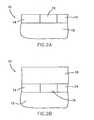
- FIG. 2Ais a diagrammatic cross-sectional view of a semiconductor wafer fragment at a preliminary step of a processing sequence.
- FIGS. 2B-2Fare views of the wafer fragment of FIG. 2A at subsequent and sequential processing steps, showing fabrication of a contact via and interconnect line by dual damascene processing according to the method of the invention, depicted in FIG. 1.
- the present inventionencompasses methods of making integrated circuits, particularly methods for forming copper contacts and interconnects using a dual damascene process.
- FIG. 1provides a process flow diagram for a first embodiment of the method of the present invention.
- a semiconductor deviceis provided that has been processed to where a first level of interconnects have been formed, and an insulating layer has been deposited ver the interconnects.
- the insulating layeris patterned to form a dual inlaid opening that extends to the underlying interconnect.
- the exposed surfaces of the insulating layere.g., SiOF
- a nitrogen plasmathat converts a portion of the insulating layer into a nitrided oxide film (e.g., SiON) that is a diffusion barrier layer for copper.
- a nitrided oxide filme.g., SiON
- a copper layeris then deposited, preferably by ionized magnetron sputtering followed by a low temperature reflow process in atomic hydrogen generated by a microwave excited Kr/H 2 . Excess copper is then removed from high regions by chemical mechanical polishing (CMP), which leaves copper only in the etched features to form the dual inlaid structures that include via and interconnect portions
- a dual damascene processis used to form copper contact vias and interconnects associated with a semiconductor circuit. It is understood that the method of the invention can be used in a single damascene process to form an interconnect and/or a via of an integrated circuit memory or microprocessor.
- interconnectsare illustrated and will be described as being coupled to a conductive area 16 ; however, the interconnects of the present invention can be used wherever required within the structure of a semiconductor circuit.
- a wafer fragment 10is shown as including a semiconductor base layer 12 , a dielectric or insulating layer 14 , and a conductive area 16 .
- the base layer 12is a semiconductor substrate, for example, a semiconductor wafer substrate or the wafer along with various process layers formed thereon, including one or more semiconductor layers or other formations, and active or operable portions of semiconductor devices.
- An exemplary base layer 12is monocrystalline silicon having regions that are p-type or n-type doped.
- the insulating layer 14for example, anoxide such as phosphosilicate glass (PSG) or borophosphosilicate glass (BPSG), in a single layer or multiple layers, is formed over the base layer 12 , being silicon in the illustrated embodiment.
- the insulating layer 14has been etched to provide an opening extending to the base layer 12 , and into which a conductive material has been deposited by chemical vapor deposition (CVD) or other suitable method, and planarized, for example, by chemical mechanical polishing (CMP), to form conductive area 16 , such as a conductive trace.
- the conductive areacan comprise a conductor or semiconductor material, for example, polysilicon, metal or doped silicon.
- the conductive areacomprises copper.
- the conductive area 16can be used for connecting power to the semiconductor base layer 12 as part of a semiconductor structure.
- a second dielectric or insulating layer 18in a single layer or multiple layers, is formed over insulating layer 14 and conductive area 16 , typically to a thickness of about 4,000 to about 10,000 angstroms (about 400 to about 1000 nm).
- the second insulating layer 18can be formed using, for example, tetraethylorthosilicate (TEOS), silicon oxyfluoride (SiOF), low k dielectrics, and the like.
- TEOStetraethylorthosilicate
- SiOFsilicon oxyfluoride
- a preferred insulating layer 18comprises SiOF, which has a low dielectric constant of 3.5.
- An SiOF insulating layer 18can be formed, for example, by introducing a fluorine species during plasma enhanced chemical vapor deposition (PECVD) of SiO 2 , or by deposition by electron cyclotron resonance (ECR) CVD.
- PECVDplasma enhanced chemical vapor deposition
- ECRelectron cycl
- the second insulating layer 18(e.g., SiOF) is patterned and etched to form dual inlaid openings that include a contact opening or via 20 and an interconnect channel or trench 22 , resulting in the structure shown in FIG. 2C. Etching of the insulating layer 18 can be performed using known techniques, preferably by reactive ion etching (RIE).
- RIEreactive ion etching
- the contact opening 20is etched through the second insulative layer 18 to extend to the underlying conductive layer 16 .
- the contact opening 20includes sidewalls 21 a and a base portion 21 b .
- the interconnect trench 22is etched into the second insulative layer 18 to align with the contact opening 20 and form a channel from the contact opening 20 to other circuit elements (not shown).
- the interconnect trench 22includes sidewalls 23 a and a base portion 23 b .
- the contact opening 20can be patterned and etched first, followed by etching of the interconnect trench 22 , or visa versa. The etch step can then followed by a resist strip step and a solvent clean step, as known and used in the art.
- the surface 24 of the insulating layer 18(e.g., SiOF) is nitrided in situ using a nitrogen-comprising plasma.
- the nitriding stepconverts a portion of the exposed surface 24 of the insulating (oxide) layer 18 (e.g., SiOF) to a nitrogen-comprising diffusion or barrier layer 26 , for example, silicon oxynitride (SiON).
- the plasma nitriding stepcan be performed by exposing the insulating layer 18 , for example, to ammonia (NH 3 ) and/or molecular nitrogen (N 2 ), to dope nitrogen into the insulating layer.
- the thickness of the nitrogen-comprising barrier layer 26e.g., SiON
- the barrier layer 26functions as a barrier to suppress out-diffusion of copper atoms into the underlying insulating (oxide) layer 18 (e.g., SiOF).
- Such nitriding techniquesare known in the art, for example, as described by Mikagi et al., the disclosure of which is incorporated by reference herein, whereby the nitriding step was performed by exposing the oxide insulating layer (e.g., SiOF) to an ammonia (NH 3 ) plasma at about 450° C. for about 30 minutes, resulting in a nitrogen-comprising barrier layer (e.g., SiON) having a thickness of about 10 nm.
- the oxide insulating layere.g., SiOF
- NH 3ammonia
- SiONnitrogen-comprising barrier layer having a thickness of about 10 nm.
- the stepis performed by exposing the oxide insulating layer (e.g., SiOF) to a relatively high power plasma, e.g., ammonia (NH 3 ) and/or nitrogen (N 2 ), in a range of about 500 to about 1,500 watts, and a pressure of about 500 to about 2,000 mTorr, for about 1 to about 3 minutes to convert about 20 to about 30 nm of the exposed oxide layer (e.g., SiOF) into the nitrogen-comprising barrier layer (e.g., SiON).
- a relatively high power plasmae.g., ammonia (NH 3 ) and/or nitrogen (N 2 )
- NH 3ammonia
- N 2nitrogen
- a copper layer 30is deposited over the exposed surface 28 of the barrier layer 26 (e.g., SiON) to completely fill the interconnect trench 22 and the contact opening 20 , resulting in the structure shown in FIG. 2E.
- the copperis deposited onto the trench 22 and contact opening 20 by sputtering, particularly ionized magnetron sputtering, also termed as ionized physical vapor deposition (I-PVD) and ion metal plasma (IMP) sputtering.
- I-PVDionized physical vapor deposition
- IMPion metal plasma
- Such sputtering techniques and process systemsare well known in the art, as described, for example, in U.S. Pat. No. 5,985,759 (Kim), the disclosure of which is incorporated by reference herein.
- the resulting metal layeris a high purity copper with low electrical resistivity.
- the copperis deposited by ionized magnetron sputtering in which sputtered copper atoms are ionized by pass through an RF source to create a high density, inductively coupled RF plasma.
- Ionized magnetron sputteringachieves directional deposition of metals, and is preferred to fill 0.25 ⁇ m and smaller contact openings having a high aspect ratio of about 3:1 or greater.
- the wafer 10is placed about 12 to about 15 cm (about 5 to about 6 inches) from a copper target cathode.
- the copper cathodeis sputtered under a pressure of about 0.5 to about 5 mTorr by applying a DC power field to an inert gas, typically argon (Ar), over a range of about 0.5 to about 8 kW, preferably about 4 kW, resulting in the emission of copper atoms.
- RF poweris applied to a 1 to 3-turn RF inductive coil in the area between the copper cathode and the wafer or other substrate.
- the RF poweris applied to the coil at a frequency of about 1.9 or 13.5 MHz and a wattage of about 0.5 to about 6 kW, preferably about 1.5 to about 4 kW.
- the RF plasmais generated using an inert gas, typically argon (Ar) at a pressure of about 30 mTorr, to create a high density, inductively coupled RF plasma (n e >10 11 cm ⁇ 3)
- Arargon
- n e >10 11 cm ⁇ 3As the sputtered copper atoms pass through the RF plasma, about 50 to about 90%, preferably about 70 to about 90% of the sputtered copper atoms are ionized.
- the copper ionsthen deposited onto the exposed surface 28 of the barrier layer 26 and into the contact opening 20 and the trench 22 .
- the preferred process for forming the copper layeris by sputtering techniques
- other means for producing copper atomscan be used.
- copper evaporation techniques for vaporizing copper for deposition using a conventional metal evaporatorcan be used. Such techniques are described, for example, in U.S. Pat. Nos. 4,944,961 (Lui) and U.S. Pat. No. 5,302,266 (Grabarz), the disclosures of which are incorporated by reference herein.
- metal evaporationuses a known method to heat the copper, including a heated filament, an electron gun, or RF induction.
- the metal evaporatorhas a port into a vacuum chamber where the wafer is placed.
- the copperis inserted into the metal evaporator, and the evaporator is heated to provide a steady flux of copper atoms through the port and into the vacuum chamber.
- the metal vaporis ionized by means of microwave energy, and the ions deposit as a layer on the exposed surface 28 of the barrier layer 26 .
- the deposited copperthen undergoes reflow processing step to ensure complete filling of narrow, high aspect ratio features.
- the deposited copper layer 30is reflowed at a low temperature in an atmosphere of atomic hydrogen to fill the trench 22 and the contact hole 20 .
- a low temperature reflowis used to avoid the copper from closing over the trench/via and forming a void, and to ensure complete filling of the contact opening and the bottom of the trench 22 .
- the copper layeris reflowed at a temperature below about 400 C., preferably at about 300 to about 350° C., more preferably at about ⁇ 320° C., for about 10 minutes.
- the atomic hydrogenenhances the reflow of the copper into the contact opening and trench.
- the irradiation of the copper film by hydrogen atoms during the reflow processreduces the reflow temperature by more than about 100° C., and prevents void formation even in 0.15 ⁇ m trenches with an aspect ratio of 3:1.
- the method of the inventionpreferably utilizes an atomic hydrogen that is generated in a mixed high density krypton/hydrogen (Kr/H 2 ) plasma using a microwave-excitation high-density plasma system at a pressure of about 1 Torr and temperature of about 400° C.
- the mixing ratio of hydrogen to inert gasis preferably about 3 to about 5% (H 2 /Kr).
- the reflowed copper layer 30 of FIG. 2Eis then polished down so that the copper only lies within the contact opening 20 and the trench 22 to provide a planarized copper interconnect, as shown in FIG. 2F, and complete the dual damascene interconnect structure.
- the copper layer 30can be polished using a convention Cu-chemical mechanical polishing (CMP) technique selective to oxide, as known and used in the art.
- CMPCu-chemical mechanical polishing
- the processresults in a dual inlaid structure that include both a via portion 20 and an interconnect channel portion 22 , for providing electrical connection to various parts of the semiconductor device.
- a passivation layer(not shown) can then be formed over the device.
- other interconnect layerscan be formed overlying the present structures.
- the foregoing processcan also be modified to a single damascene process to form only interconnect channels 22 .
Landscapes
- Engineering & Computer Science (AREA)
- Physics & Mathematics (AREA)
- Condensed Matter Physics & Semiconductors (AREA)
- General Physics & Mathematics (AREA)
- Manufacturing & Machinery (AREA)
- Computer Hardware Design (AREA)
- Microelectronics & Electronic Packaging (AREA)
- Power Engineering (AREA)
- Plasma & Fusion (AREA)
- Internal Circuitry In Semiconductor Integrated Circuit Devices (AREA)
Abstract
Description
- The invention relates generally to semiconductor devices, and more particularly to interconnections within semiconductor circuits and methods of making the interconnections, including methods for fabricating copper interconnects.[0001]
- Integrated circuits are interconnected networks of resistors, transistors and other electrical components that are generally formed on a silicon substrate or wafer with conductive, insulative and semiconductive materials. Fabricating integrated circuits involves forming electrical components at a number of layers and different locations. The various components are then wired or interconnected together to form a memory or other electric circuit. Typically, the components are connected together by interlayer contact openings or vias formed through a dielectric layer to an underlying component and by conductive lines formed in trenches in the dielectric layer that extend from the via to one or more other vias in the layer. The trenches and vias are typically filled with aluminum, tungsten, copper, gold, silver, polysilicon, or other suitable conductive material.[0002]
- The never-ending miniaturization of integrated circuits (IC) is leading to denser and finer pitched chips with ever increasing speed and performance. In order to enhance the performance of advanced integrated circuits, the interconnect systems are gradually migrating from aluminum-based metallurgy to higher-conductivity and more electromigration-resistant copper.[0003]
- Of the several schemes proposed for fabricating copper interconnects, the most promising method appears to be the damascene process. In a single damascene process, channels or trenches are etched into the dielectric layer, and a metal is deposited to fill the etched trenches forming an interconnect line. In a dual damascene process, both the via and trenches are etched in the dielectric layer overlying an underlying interconnect or trace. The desired metal is then deposited into the trenches and holes in one step to form a dual damascene structure. Chemical mechanical polishing (CMP) is used to remove the unwanted surface metal, while leaving the desired metal in the trenches and holes, thus forming inlaid interconnect lines and vias that are coupled to electrical components beneath the insulation layer. The CMP processing leaves a planarized surface for subsequent metallization to build multi-level interconnections.[0004]
- The introduction of copper conductors in integrated circuits has received wide publicity. Copper interconnect is the most promising metallization scheme for future generation high-speed ULSI, primarily because of lower electrical resistivity (1.7 vs. 2.3 μΩcm) and more electro/stress-migration resistance than the conventional aluminum-based materials. Full, 6-level copper wiring has now been introduced in a sub-025 μm CMOS ULSI technology. However, copper atoms can easily diffuse through most oxides into the devices in the underlying silicon substrate and act as recombination centers to spoil device performance. Copper also diffuses into commonly used dielectric materials (i.e., SiO[0005]2) and certain polymers, resulting in conductivity of these insulators and higher effective dielectric constants.
- Based on the foregoing, a suitable diffusion barrier is needed in order to adopt copper interconnects for ULSI. A variety of barrier materials such as tantalum (Ta), tantalum silicon nitride (TaSiN), titanium nitride (TiN), tantalum nitride (TaN) and tungsten nitride (WN) have been investigated.[0006]
- These barrier films are generally deposited by sputtering to a thickness range of 20 to 30 nm and higher. If the barrier thickness does not scale with the device (and wiring scaling), the impact on electrical resistance is significant. The resistance increase due to liner (diffusion barrier) thickness becomes substantial for line widths of approximately 0.2 μm and below. It has been reported that a very thin (<6 nm) tungsten silicon nitride (WSiN) layer formed by electron cyclotron resonance (ECR) plasma nitridation of sputtered WSi film prevented copper diffusion.[0007]
- A barrier metal free copper damascene interconnection technology has been reported. The scheme involved formation of a thin barrier layer on the surface of silicon oxyfluoride (SiOF) film by ammonia (NH[0008]3) plasma treatment. The reflow of copper was then performed at 400° C. in atmospheric gas composed of N2/H2.
- It would be desirable to provide a process for the formation of conductive contacts and interconnect lines that eliminates the need for depositing a metal barrier diffusion layer and results in a conductive contact/interconnect that has a higher purity and a lower resistivity compared to prior art films and contact structures.[0009]
- The present invention provides methods for forming conductive contacts in a semiconductor structure, and the conductive components formed by those methods. In particular, the method is used to fabricate copper contacts and interconnects in integrated circuits such as memory devices. The method can be used to form single or dual damascene copper interconnects and vias in the manufacture of integrated circuits.[0010]
- The method of the invention involves forming a conductive component in a semiconductor device. In one embodiment, the method comprises providing a substrate with an overlying insulating layer that includes at least one opening formed therein. A non-metal barrier layer is formed over the insulating layer, including over the sidewalls and bottom portion or base of the opening, by exposing the insulating layer to a nitrogen-containing plasma, preferably ammonia (NH[0011]3), to transform the exposed surface of the insulating layer to the barrier layer, preferably to a thickness of about 5 nm to about 10 nm to prevent diffusion of the conductive material into the insulating layer. In a preferred embodiment, the insulating layer comprises silicon oxyfluoride (SiOF), and the barrier layer comprises silicon oxynitride (SiON). A conductive material (i.e., copper) is directionally deposited into the opening, preferably by ionized magnetron sputtering. To ensure filling of the opening, the conductive material is then reflowed at a temperature of less than about 400° C., preferably at a temperature of about 300 to about 350° C., in the presence of atomic hydrogen that is preferably generated using a microwave-excitation high density plasma system using a krypton/hydrogen plasma. After depositing the conductive layer, excess conductive material is removed, preferably by chemical-mechanical polishing, to form the conductive contact in the opening. The method is useful for forming a contact to a semiconductor component underlying the insulating layer on a substrate, for fabricating a semiconductor circuit and an integrated circuit.
- In another embodiment, the method can be used to form a dual damascene conductive structure in a semiconductor device by providing a substrate comprising a semiconductor component and an insulating layer over the semiconductor component, and etching the insulating layer to form a channel corresponding to a trench along the insulating layer, and an opening extending from the trench to the semiconductor component. A non-metal barrier layer is formed over the insulating layer including the exposed surface of the channel and the opening, and a conductive material is deposited on the barrier layer by ionized magnetron sputtering to fill the channel and the opening to form dual damascene conductive structures in the insulating layer. The dual damascene structures resulting from the process comprise an interconnect line coupled to a conductive contact to the semiconductor component. The barrier layer prevents diffusion of the copper into the insulating layer.[0012]
- Another aspect is a semiconductor circuit resulting from the method of the invention. The semiconductor circuit comprises a semiconductor structure; an insulating layer formed over the semiconductor structure with an opening formed through the insulating layer to the semiconductor structure and/or a horizontal trench opening extending over the insulating layer; a non-metal-comprising barrier layer formed over the insulating layer including the surface of the contact opening and/or the trench opening, which prevents diffusion of a copper-comprising material into the insulating layer, and a conductive contact formed in the contact opening and/or the trench opening over the barrier layer, and coupled to the semiconductor structure. The conductive contact comprises copper sputtered into the contact opening and/or the trench opening and reflowed at a temperature less than about 400° C. in the presence of atomic hydrogen.[0013]
- In another embodiment, the semiconductor circuit comprises a semiconductor structure; an insulating layer formed over the semiconductor structure and having a plurality of generally vertical contact openings extending therethrough to contact locations on the semiconductor structure, and a plurality of generally horizontal trench openings extending over the insulating layer; each of the contact openings and trench openings having a non-metal barrier layer formed on a surface; a plurality of generally vertical conductive contacts formed through the contact openings and coupled to the semiconductor structure; and a plurality of generally horizontal conductive interconnect lines formed in the trench openings, each of the interconnect lines coupled to at least one generally vertical conductive contact. The conductive contacts and/or the interconnect lines comprise copper deposited by ionized sputtering into the contact opening or the trench opening over the barrier layer and reflowed at a temperature less than about 400° C. in the presence of atomic hydrogen to fill the contact opening and/or the trench opening.[0014]
- Another aspect is an integrated circuit memory or microprocessor resulting from the method of the invention. The integrated circuit memory or microprocessor comprises an array of memory and/or logic cells, internal circuitry, and conductive contacts and interconnects coupled to the memory or logic arrays and internal circuitry. The metal contacts and interconnects comprise a one or more generally horizontal conductive interconnect lines extending over an insulating layer overlying the memory array, and one or more generally vertical conductive contact, whereby each interconnect line is coupled to at least one generally vertical conductive contact. The conductive interconnect and/or the conductive contact comprises copper deposited by ionized sputtering over a non-metal-comprising barrier layer overlying the surface of a trench opening extending over the insulating layer and/or a contact opening extending vertically into the insulating layer. The deposited copper is preferably reflowed at a temperature less than about 400° C. in the presence of atomic hydrogen to fill the trench opening and/or the contact opening. Preferably, the metal contacts and interconnects are formed using a dual damascene process.[0015]
- Advantageously, the present invention provides higher purity copper contacts and interconnects having a lower resistivity (greater conductivity) compared to prior art copper films and contact structures. The method advantageously eliminates void formation in sub-micron trenches and contact openings, and other high aspect ratio conductive features. The process also eliminates the need to form a separate diffusion barrier by transforming a portion of the insulating layer to form a diffusion barrier film or layer between the metal (copper) contact/interconnect and the insulating layer.[0016]
- Preferred embodiments of the invention are described below with reference to the following accompanying drawings, which are for illustrative purposes only. Throughout the following views, the reference numerals will be used in the drawings, and the same reference numerals will be used throughout the several views and in the description to indicate same or like parts.[0017]
- FIG. 1 is a process flow diagram for an embodiment of the method of the present invention.[0018]
- FIG. 2A is a diagrammatic cross-sectional view of a semiconductor wafer fragment at a preliminary step of a processing sequence.[0019]
- FIGS. 2B-2F are views of the wafer fragment of FIG. 2A at subsequent and sequential processing steps, showing fabrication of a contact via and interconnect line by dual damascene processing according to the method of the invention, depicted in FIG. 1.[0020]
- The present invention encompasses methods of making integrated circuits, particularly methods for forming copper contacts and interconnects using a dual damascene process.[0021]
- The method of the invention will be described generally with reference to the drawings for the purpose of illustrating the present preferred embodiments of the invention only and not for purposes of limiting the same. The figures illustrate processing steps for use in the fabrication of semiconductor devices in accordance with the present invention. It should be readily apparent that the processing steps are only a portion of the entire fabrication process. The present invention particularly deals with the method of fabricating contacts and interconnects that are used in the fabrication of semiconductor devices.[0022]
- FIG. 1 provides a process flow diagram for a first embodiment of the method of the present invention. A semiconductor device is provided that has been processed to where a first level of interconnects have been formed, and an insulating layer has been deposited ver the interconnects. The insulating layer is patterned to form a dual inlaid opening that extends to the underlying interconnect. The exposed surfaces of the insulating layer (e.g., SiOF) are then exposed to a nitrogen plasma that converts a portion of the insulating layer into a nitrided oxide film (e.g., SiON) that is a diffusion barrier layer for copper. A copper layer is then deposited, preferably by ionized magnetron sputtering followed by a low temperature reflow process in atomic hydrogen generated by a microwave excited Kr/H[0023]2. Excess copper is then removed from high regions by chemical mechanical polishing (CMP), which leaves copper only in the etched features to form the dual inlaid structures that include via and interconnect portions
- The process is described in more detail with reference to FIGS. 2A-2F. As shown, a dual damascene process is used to form copper contact vias and interconnects associated with a semiconductor circuit. It is understood that the method of the invention can be used in a single damascene process to form an interconnect and/or a via of an integrated circuit memory or microprocessor.[0024]
- The interconnects are illustrated and will be described as being coupled to a[0025]
conductive area 16; however, the interconnects of the present invention can be used wherever required within the structure of a semiconductor circuit. - Referring to FIG. 2A, a[0026]
wafer fragment 10 is shown as including asemiconductor base layer 12, a dielectric or insulatinglayer 14, and aconductive area 16. Thebase layer 12 is a semiconductor substrate, for example, a semiconductor wafer substrate or the wafer along with various process layers formed thereon, including one or more semiconductor layers or other formations, and active or operable portions of semiconductor devices. Anexemplary base layer 12 is monocrystalline silicon having regions that are p-type or n-type doped. The insulatinglayer 14, for example, anoxide such as phosphosilicate glass (PSG) or borophosphosilicate glass (BPSG), in a single layer or multiple layers, is formed over thebase layer 12, being silicon in the illustrated embodiment. The insulatinglayer 14 has been etched to provide an opening extending to thebase layer 12, and into which a conductive material has been deposited by chemical vapor deposition (CVD) or other suitable method, and planarized, for example, by chemical mechanical polishing (CMP), to formconductive area 16, such as a conductive trace. The conductive area can comprise a conductor or semiconductor material, for example, polysilicon, metal or doped silicon. Preferably, the conductive area comprises copper. Theconductive area 16 can be used for connecting power to thesemiconductor base layer 12 as part of a semiconductor structure. - Referring to FIG. 2B, a second dielectric or insulating[0027]
layer 18, in a single layer or multiple layers, is formed over insulatinglayer 14 andconductive area 16, typically to a thickness of about 4,000 to about 10,000 angstroms (about 400 to about 1000 nm). The second insulatinglayer 18 can be formed using, for example, tetraethylorthosilicate (TEOS), silicon oxyfluoride (SiOF), low k dielectrics, and the like. A preferred insulatinglayer 18 comprises SiOF, which has a low dielectric constant of 3.5. AnSiOF insulating layer 18 can be formed, for example, by introducing a fluorine species during plasma enhanced chemical vapor deposition (PECVD) of SiO2, or by deposition by electron cyclotron resonance (ECR) CVD. - The second insulating layer[0028]18 (e.g., SiOF) is patterned and etched to form dual inlaid openings that include a contact opening or via20 and an interconnect channel or
trench 22, resulting in the structure shown in FIG. 2C. Etching of the insulatinglayer 18 can be performed using known techniques, preferably by reactive ion etching (RIE). Thecontact opening 20 is etched through thesecond insulative layer 18 to extend to the underlyingconductive layer 16. Thecontact opening 20 includes sidewalls21aand abase portion 21b. Theinterconnect trench 22 is etched into thesecond insulative layer 18 to align with thecontact opening 20 and form a channel from thecontact opening 20 to other circuit elements (not shown). Theinterconnect trench 22 includes sidewalls23aand abase portion 23b. Thecontact opening 20 can be patterned and etched first, followed by etching of theinterconnect trench 22, or visa versa. The etch step can then followed by a resist strip step and a solvent clean step, as known and used in the art. - After the[0029]
interconnect trench 22 andcontact opening 20 are formed, thesurface 24 of the insulating layer18 (e.g., SiOF) is nitrided in situ using a nitrogen-comprising plasma. As depicted in FIG. 2D, the nitriding step converts a portion of the exposedsurface 24 of the insulating (oxide) layer18 (e.g., SiOF) to a nitrogen-comprising diffusion orbarrier layer 26, for example, silicon oxynitride (SiON). The plasma nitriding step can be performed by exposing the insulatinglayer 18, for example, to ammonia (NH3) and/or molecular nitrogen (N2), to dope nitrogen into the insulating layer. Preferably, the thickness of the nitrogen-comprising barrier layer26 (e.g., SiON) is about 5 to about 10 nm. The barrier layer26 (e.g., SiON) functions as a barrier to suppress out-diffusion of copper atoms into the underlying insulating (oxide) layer18 (e.g., SiOF). - Such nitriding techniques are known in the art, for example, as described by Mikagi et al., the disclosure of which is incorporated by reference herein, whereby the nitriding step was performed by exposing the oxide insulating layer (e.g., SiOF) to an ammonia (NH[0030]3) plasma at about 450° C. for about 30 minutes, resulting in a nitrogen-comprising barrier layer (e.g., SiON) having a thickness of about 10 nm.
- Another nitriding technique is described in U.S. Pat. No. 5,821,168 (Jain), the disclosure of which is incorporated by reference herein. The step is performed by exposing the oxide insulating layer (e.g., SiOF) to a relatively high power plasma, e.g., ammonia (NH[0031]3) and/or nitrogen (N2), in a range of about 500 to about 1,500 watts, and a pressure of about 500 to about 2,000 mTorr, for about 1 to about 3 minutes to convert about 20 to about 30 nm of the exposed oxide layer (e.g., SiOF) into the nitrogen-comprising barrier layer (e.g., SiON).
- After the insulating[0032]
layer 18 is nitrided, acopper layer 30 is deposited over the exposed surface28 of the barrier layer26 (e.g., SiON) to completely fill theinterconnect trench 22 and thecontact opening 20, resulting in the structure shown in FIG. 2E. According to the invention, the copper is deposited onto thetrench 22 andcontact opening 20 by sputtering, particularly ionized magnetron sputtering, also termed as ionized physical vapor deposition (I-PVD) and ion metal plasma (IMP) sputtering. Such sputtering techniques and process systems are well known in the art, as described, for example, in U.S. Pat. No. 5,985,759 (Kim), the disclosure of which is incorporated by reference herein. The resulting metal layer is a high purity copper with low electrical resistivity. - Kin a preferred method, the copper is deposited by ionized magnetron sputtering in which sputtered copper atoms are ionized by pass through an RF source to create a high density, inductively coupled RF plasma. Ionized magnetron sputtering achieves directional deposition of metals, and is preferred to fill 0.25 μm and smaller contact openings having a high aspect ratio of about 3:1 or greater.[0033]
- Ian a exmplary ionized magnetron sputtering process using a conventional ionized PVD reactor (not shown), the[0034]
wafer 10 is placed about 12 to about 15 cm (about 5 to about 6 inches) from a copper target cathode. The copper cathode is sputtered under a pressure of about 0.5 to about 5 mTorr by applying a DC power field to an inert gas, typically argon (Ar), over a range of about 0.5 to about 8 kW, preferably about 4 kW, resulting in the emission of copper atoms. RF power is applied to a 1 to 3-turn RF inductive coil in the area between the copper cathode and the wafer or other substrate. The RF power is applied to the coil at a frequency of about 1.9 or 13.5 MHz and a wattage of about 0.5 to about 6 kW, preferably about 1.5 to about 4 kW. The RF plasma is generated using an inert gas, typically argon (Ar) at a pressure of about 30 mTorr, to create a high density, inductively coupled RF plasma (ne>1011cm−3) As the sputtered copper atoms pass through the RF plasma, about 50 to about 90%, preferably about 70 to about 90% of the sputtered copper atoms are ionized. The copper ions then deposited onto the exposed surface28 of thebarrier layer 26 and into thecontact opening 20 and thetrench 22. Although the preferred process for forming the copper layer is by sputtering techniques, other means for producing copper atoms can be used. For example, copper evaporation techniques for vaporizing copper for deposition using a conventional metal evaporator, can be used. Such techniques are described, for example, in U.S. Pat. Nos. 4,944,961 (Lui) and U.S. Pat. No. 5,302,266 (Grabarz), the disclosures of which are incorporated by reference herein. - In general, metal evaporation uses a known method to heat the copper, including a heated filament, an electron gun, or RF induction. The metal evaporator has a port into a vacuum chamber where the wafer is placed. The copper is inserted into the metal evaporator, and the evaporator is heated to provide a steady flux of copper atoms through the port and into the vacuum chamber. The metal vapor is ionized by means of microwave energy, and the ions deposit as a layer on the exposed surface[0035]28 of the
barrier layer 26. - The deposited copper then undergoes reflow processing step to ensure complete filling of narrow, high aspect ratio features. According to the invention, the deposited[0036]
copper layer 30 is reflowed at a low temperature in an atmosphere of atomic hydrogen to fill thetrench 22 and thecontact hole 20. - A low temperature reflow is used to avoid the copper from closing over the trench/via and forming a void, and to ensure complete filling of the contact opening and the bottom of the[0037]
trench 22. To that end, the copper layer is reflowed at a temperature below about 400 C., preferably at about 300 to about 350° C., more preferably at about −320° C., for about 10 minutes. - The atomic hydrogen enhances the reflow of the copper into the contact opening and trench. The irradiation of the copper film by hydrogen atoms during the reflow process reduces the reflow temperature by more than about 100° C., and prevents void formation even in 0.15 μm trenches with an aspect ratio of 3:1. The method of the invention preferably utilizes an atomic hydrogen that is generated in a mixed high density krypton/hydrogen (Kr/H[0038]2) plasma using a microwave-excitation high-density plasma system at a pressure of about 1 Torr and temperature of about 400° C. The mixing ratio of hydrogen to inert gas is preferably about 3 to about 5% (H2/Kr).
- The reflowed[0039]
copper layer 30 of FIG. 2E is then polished down so that the copper only lies within thecontact opening 20 and thetrench 22 to provide a planarized copper interconnect, as shown in FIG. 2F, and complete the dual damascene interconnect structure. Thecopper layer 30 can be polished using a convention Cu-chemical mechanical polishing (CMP) technique selective to oxide, as known and used in the art. - The process results in a dual inlaid structure that include both a via[0040]
portion 20 and aninterconnect channel portion 22, for providing electrical connection to various parts of the semiconductor device. A passivation layer (not shown) can then be formed over the device. Optionally, although not shown, other interconnect layers can be formed overlying the present structures. The foregoing process can also be modified to a single damascene process to formonly interconnect channels 22. - In compliance with the statute, the invention has been described in language more or less specific as to structural and methodical features. It is to be understood, however, that the invention is not limited to the specific features shown and described, since the means herein disclosed comprise preferred forms of putting the invention into effect. The invention is, therefore, claimed in any of its forms or modifications within the proper scope of the appended claims appropriately interpreted in accordance with the doctrine of equivalents.[0041]
Claims (82)
Priority Applications (5)
| Application Number | Priority Date | Filing Date | Title |
|---|---|---|---|
| US10/889,203US7186643B2 (en) | 2001-03-15 | 2004-07-12 | Barrier-metal-free copper damascene technology using atomic hydrogen enhanced reflow |
| US11/511,652US7605468B2 (en) | 2001-03-15 | 2006-08-29 | Barrier-metal-free copper damascene technology using atomic hydrogen enhanced reflow |
| US12/553,691US7888261B2 (en) | 2001-03-15 | 2009-09-03 | Barrier-metal-free copper damascene technology using atomic hydrogen enhanced reflow |
| US13/005,231US8211792B2 (en) | 2001-03-15 | 2011-01-12 | Barrier-metal-free copper damascene technology using atomic hydrogen enhanced reflow |
| US13/484,824US8513112B2 (en) | 2001-03-15 | 2012-05-31 | Barrier-metal-free copper damascene technology using enhanced reflow |
Applications Claiming Priority (3)
| Application Number | Priority Date | Filing Date | Title |
|---|---|---|---|
| US09/809,670US6696360B2 (en) | 2001-03-15 | 2001-03-15 | Barrier-metal-free copper damascene technology using atomic hydrogen enhanced reflow |
| US10/122,870US6762500B2 (en) | 2001-03-15 | 2002-04-15 | Barrier-metal-free copper damascene technology using atomic hydrogen enhanced reflow |
| US10/889,203US7186643B2 (en) | 2001-03-15 | 2004-07-12 | Barrier-metal-free copper damascene technology using atomic hydrogen enhanced reflow |
Related Parent Applications (1)
| Application Number | Title | Priority Date | Filing Date |
|---|---|---|---|
| US10/122,870ContinuationUS6762500B2 (en) | 2001-03-15 | 2002-04-15 | Barrier-metal-free copper damascene technology using atomic hydrogen enhanced reflow |
Related Child Applications (1)
| Application Number | Title | Priority Date | Filing Date |
|---|---|---|---|
| US11/511,652DivisionUS7605468B2 (en) | 2001-03-15 | 2006-08-29 | Barrier-metal-free copper damascene technology using atomic hydrogen enhanced reflow |
Publications (2)
| Publication Number | Publication Date |
|---|---|
| US20040248398A1true US20040248398A1 (en) | 2004-12-09 |
| US7186643B2 US7186643B2 (en) | 2007-03-06 |
Family
ID=25201937
Family Applications (7)
| Application Number | Title | Priority Date | Filing Date |
|---|---|---|---|
| US09/809,670Expired - Fee RelatedUS6696360B2 (en) | 2001-03-15 | 2001-03-15 | Barrier-metal-free copper damascene technology using atomic hydrogen enhanced reflow |
| US10/122,870Expired - Fee RelatedUS6762500B2 (en) | 2001-03-15 | 2002-04-15 | Barrier-metal-free copper damascene technology using atomic hydrogen enhanced reflow |
| US10/889,203Expired - Fee RelatedUS7186643B2 (en) | 2001-03-15 | 2004-07-12 | Barrier-metal-free copper damascene technology using atomic hydrogen enhanced reflow |
| US11/511,652Expired - Fee RelatedUS7605468B2 (en) | 2001-03-15 | 2006-08-29 | Barrier-metal-free copper damascene technology using atomic hydrogen enhanced reflow |
| US12/553,691Expired - Fee RelatedUS7888261B2 (en) | 2001-03-15 | 2009-09-03 | Barrier-metal-free copper damascene technology using atomic hydrogen enhanced reflow |
| US13/005,231Expired - Fee RelatedUS8211792B2 (en) | 2001-03-15 | 2011-01-12 | Barrier-metal-free copper damascene technology using atomic hydrogen enhanced reflow |
| US13/484,824Expired - Fee RelatedUS8513112B2 (en) | 2001-03-15 | 2012-05-31 | Barrier-metal-free copper damascene technology using enhanced reflow |
Family Applications Before (2)
| Application Number | Title | Priority Date | Filing Date |
|---|---|---|---|
| US09/809,670Expired - Fee RelatedUS6696360B2 (en) | 2001-03-15 | 2001-03-15 | Barrier-metal-free copper damascene technology using atomic hydrogen enhanced reflow |
| US10/122,870Expired - Fee RelatedUS6762500B2 (en) | 2001-03-15 | 2002-04-15 | Barrier-metal-free copper damascene technology using atomic hydrogen enhanced reflow |
Family Applications After (4)
| Application Number | Title | Priority Date | Filing Date |
|---|---|---|---|
| US11/511,652Expired - Fee RelatedUS7605468B2 (en) | 2001-03-15 | 2006-08-29 | Barrier-metal-free copper damascene technology using atomic hydrogen enhanced reflow |
| US12/553,691Expired - Fee RelatedUS7888261B2 (en) | 2001-03-15 | 2009-09-03 | Barrier-metal-free copper damascene technology using atomic hydrogen enhanced reflow |
| US13/005,231Expired - Fee RelatedUS8211792B2 (en) | 2001-03-15 | 2011-01-12 | Barrier-metal-free copper damascene technology using atomic hydrogen enhanced reflow |
| US13/484,824Expired - Fee RelatedUS8513112B2 (en) | 2001-03-15 | 2012-05-31 | Barrier-metal-free copper damascene technology using enhanced reflow |
Country Status (1)
| Country | Link |
|---|---|
| US (7) | US6696360B2 (en) |
Cited By (34)
| Publication number | Priority date | Publication date | Assignee | Title |
|---|---|---|---|---|
| US20060110902A1 (en)* | 2004-11-24 | 2006-05-25 | Semiconductor Manufacturing International (Shanghai) Corporation | Method and system for metal barrier and seed integration |
| US20070052096A1 (en)* | 2005-08-23 | 2007-03-08 | Taiwan Semiconductor Manufacturing Co., Ltd. | Semiconductor device and method for forming the same |
| US7235501B2 (en) | 2004-12-13 | 2007-06-26 | Micron Technology, Inc. | Lanthanum hafnium oxide dielectrics |
| US7312494B2 (en) | 2003-06-24 | 2007-12-25 | Micron Technology, Inc. | Lanthanide oxide / hafnium oxide dielectric layers |
| US7326980B2 (en) | 2002-08-28 | 2008-02-05 | Micron Technology, Inc. | Devices with HfSiON dielectric films which are Hf-O rich |
| US7388246B2 (en) | 2002-08-29 | 2008-06-17 | Micron Technology, Inc. | Lanthanide doped TiOx dielectric films |
| US7402876B2 (en) | 2002-12-04 | 2008-07-22 | Micron Technology, Inc. | Zr— Sn—Ti—O films |
| US7405454B2 (en) | 2003-03-04 | 2008-07-29 | Micron Technology, Inc. | Electronic apparatus with deposited dielectric layers |
| US7410668B2 (en) | 2001-03-01 | 2008-08-12 | Micron Technology, Inc. | Methods, systems, and apparatus for uniform chemical-vapor depositions |
| US7410910B2 (en) | 2005-08-31 | 2008-08-12 | Micron Technology, Inc. | Lanthanum aluminum oxynitride dielectric films |
| US7439194B2 (en) | 2002-08-15 | 2008-10-21 | Micron Technology, Inc. | Lanthanide doped TiOx dielectric films by plasma oxidation |
| US7446368B2 (en) | 2001-08-30 | 2008-11-04 | Micron Technology, Inc. | Deposition of metal oxide and/or low asymmetrical tunnel barrier interpoly insulators |
| US7510983B2 (en) | 2005-06-14 | 2009-03-31 | Micron Technology, Inc. | Iridium/zirconium oxide structure |
| US7554161B2 (en) | 2002-06-05 | 2009-06-30 | Micron Technology, Inc. | HfAlO3 films for gate dielectrics |
| US7560395B2 (en) | 2005-01-05 | 2009-07-14 | Micron Technology, Inc. | Atomic layer deposited hafnium tantalum oxide dielectrics |
| US7560793B2 (en) | 2002-05-02 | 2009-07-14 | Micron Technology, Inc. | Atomic layer deposition and conversion |
| US7572695B2 (en) | 2005-05-27 | 2009-08-11 | Micron Technology, Inc. | Hafnium titanium oxide films |
| US7601649B2 (en) | 2004-08-02 | 2009-10-13 | Micron Technology, Inc. | Zirconium-doped tantalum oxide films |
| US7605030B2 (en) | 2006-08-31 | 2009-10-20 | Micron Technology, Inc. | Hafnium tantalum oxynitride high-k dielectric and metal gates |
| US7611959B2 (en) | 2002-12-04 | 2009-11-03 | Micron Technology, Inc. | Zr-Sn-Ti-O films |
| US7625794B2 (en) | 2003-03-31 | 2009-12-01 | Micron Technology, Inc. | Methods of forming zirconium aluminum oxide |
| US7662729B2 (en) | 2005-04-28 | 2010-02-16 | Micron Technology, Inc. | Atomic layer deposition of a ruthenium layer to a lanthanide oxide dielectric layer |
| US7670646B2 (en) | 2002-05-02 | 2010-03-02 | Micron Technology, Inc. | Methods for atomic-layer deposition |
| US7687409B2 (en) | 2005-03-29 | 2010-03-30 | Micron Technology, Inc. | Atomic layer deposited titanium silicon oxide films |
| US7709402B2 (en) | 2006-02-16 | 2010-05-04 | Micron Technology, Inc. | Conductive layers for hafnium silicon oxynitride films |
| US7719065B2 (en) | 2004-08-26 | 2010-05-18 | Micron Technology, Inc. | Ruthenium layer for a dielectric layer containing a lanthanide oxide |
| US20100171197A1 (en)* | 2009-01-05 | 2010-07-08 | Hung-Pin Chang | Isolation Structure for Stacked Dies |
| US7867919B2 (en) | 2004-08-31 | 2011-01-11 | Micron Technology, Inc. | Method of fabricating an apparatus having a lanthanum-metal oxide dielectric layer |
| US20110068466A1 (en)* | 2009-09-22 | 2011-03-24 | Taiwan Semiconductor Manufacturing Company, Ltd. | Wafer Backside Interconnect Structure Connected to TSVs |
| US8501563B2 (en) | 2005-07-20 | 2013-08-06 | Micron Technology, Inc. | Devices with nanocrystals and methods of formation |
| US8841773B2 (en) | 2010-03-30 | 2014-09-23 | Taiwan Semiconductor Manufacturing Company, Ltd. | Multi-layer interconnect structure for stacked dies |
| US8900994B2 (en) | 2011-06-09 | 2014-12-02 | Taiwan Semiconductor Manufacturing Company, Ltd. | Method for producing a protective structure |
| US9286917B1 (en)* | 2015-04-30 | 2016-03-15 | Seagate Technology Llc | Write pole formed with evaporation deposition |
| US9312225B2 (en) | 2008-12-10 | 2016-04-12 | Taiwan Semiconductor Manufacturing Company, Ltd. | Bump structure for stacked dies |
Families Citing this family (42)
| Publication number | Priority date | Publication date | Assignee | Title |
|---|---|---|---|---|
| US6696360B2 (en)* | 2001-03-15 | 2004-02-24 | Micron Technology, Inc. | Barrier-metal-free copper damascene technology using atomic hydrogen enhanced reflow |
| US6979903B1 (en)* | 2001-06-04 | 2005-12-27 | Advanced Micro Devices, Inc. | Integrated circuit with dielectric diffusion barrier layer formed between interconnects and interlayer dielectric layers |
| US6984574B2 (en)* | 2002-01-23 | 2006-01-10 | Mosel Vitelic, Inc. | Cobalt silicide fabrication using protective titanium |
| US6548401B1 (en)* | 2002-01-23 | 2003-04-15 | Micron Technology, Inc. | Semiconductor processing methods, and semiconductor constructions |
| US7687917B2 (en)* | 2002-05-08 | 2010-03-30 | Nec Electronics Corporation | Single damascene structure semiconductor device having silicon-diffused metal wiring layer |
| JP2004207281A (en)* | 2002-12-20 | 2004-07-22 | Fujitsu Ltd | Multilayer wiring structure, method of forming the same, and semiconductor device |
| US6875693B1 (en)* | 2003-03-26 | 2005-04-05 | Lsi Logic Corporation | Via and metal line interface capable of reducing the incidence of electro-migration induced voids |
| US7151315B2 (en)* | 2003-06-11 | 2006-12-19 | Taiwan Semiconductor Manufacturing Company, Ltd. | Method of a non-metal barrier copper damascene integration |
| US6991979B2 (en)* | 2003-09-22 | 2006-01-31 | International Business Machines Corporation | Method for avoiding oxide undercut during pre-silicide clean for thin spacer FETs |
| KR100571405B1 (en)* | 2003-12-24 | 2006-04-14 | 동부아남반도체 주식회사 | Device Separator Formation Method of Semiconductor Device |
| CN100461366C (en)* | 2003-12-30 | 2009-02-11 | 中芯国际集成电路制造(上海)有限公司 | Method and structure of capacitor fabrication in damascene copper process for integrated circuit devices |
| US7169698B2 (en)* | 2004-01-14 | 2007-01-30 | International Business Machines Corporation | Sacrificial inorganic polymer intermetal dielectric damascene wire and via liner |
| US7674706B2 (en)* | 2004-04-13 | 2010-03-09 | Fei Company | System for modifying small structures using localized charge transfer mechanism to remove or deposit material |
| US7294574B2 (en)* | 2004-08-09 | 2007-11-13 | Applied Materials, Inc. | Sputter deposition and etching of metallization seed layer for overhang and sidewall improvement |
| US7820020B2 (en)* | 2005-02-03 | 2010-10-26 | Applied Materials, Inc. | Apparatus for plasma-enhanced physical vapor deposition of copper with RF source power applied through the workpiece with a lighter-than-copper carrier gas |
| JP4516447B2 (en)* | 2005-02-24 | 2010-08-04 | ルネサスエレクトロニクス株式会社 | Manufacturing method of semiconductor device |
| US7538434B2 (en)* | 2005-03-08 | 2009-05-26 | Taiwan Semiconductor Manufacturing Company, Ltd. | Copper interconnection with conductive polymer layer and method of forming the same |
| JP5023505B2 (en)* | 2006-02-09 | 2012-09-12 | 東京エレクトロン株式会社 | Film forming method, plasma film forming apparatus, and storage medium |
| US7608538B2 (en)* | 2007-01-05 | 2009-10-27 | International Business Machines Corporation | Formation of vertical devices by electroplating |
| JP4110192B1 (en)* | 2007-02-23 | 2008-07-02 | キヤノン株式会社 | Photoelectric conversion device and imaging system using photoelectric conversion device |
| US20090117731A1 (en)* | 2007-11-01 | 2009-05-07 | Taiwan Semiconductor Manufacturing Co., Ltd. | Semiconductor interconnection structure and method for making the same |
| TWI525773B (en)* | 2008-07-03 | 2016-03-11 | Kobe Steel Ltd | Wiring structure, thin film transistor substrate, manufacturing method thereof, and display device |
| US8436252B2 (en)* | 2009-06-30 | 2013-05-07 | Ibiden Co., Ltd. | Printed wiring board and method for manufacturing the same |
| US9064712B2 (en) | 2010-08-12 | 2015-06-23 | Freescale Semiconductor Inc. | Monolithic microwave integrated circuit |
| US10128206B2 (en)* | 2010-10-14 | 2018-11-13 | Taiwan Semiconductor Manufacturing Company, Ltd. | Conductive pillar structure |
| US8524599B2 (en) | 2011-03-17 | 2013-09-03 | Micron Technology, Inc. | Methods of forming at least one conductive element and methods of forming a semiconductor structure |
| US8525339B2 (en) | 2011-07-27 | 2013-09-03 | International Business Machines Corporation | Hybrid copper interconnect structure and method of fabricating same |
| US9255339B2 (en) | 2011-09-19 | 2016-02-09 | Fei Company | Localized, in-vacuum modification of small structures |
| TW201532247A (en) | 2013-10-16 | 2015-08-16 | Conversant Intellectual Property Man Inc | A cost-effective method of forming embedded dynamic random access memory capacitors |
| CN103839604A (en)* | 2014-02-26 | 2014-06-04 | 京东方科技集团股份有限公司 | Heat conducting film, manufacturing method of heat conducting film, and array substrate |
| US9685370B2 (en) | 2014-12-18 | 2017-06-20 | Globalfoundries Inc. | Titanium tungsten liner used with copper interconnects |
| US10199461B2 (en)* | 2015-10-27 | 2019-02-05 | Texas Instruments Incorporated | Isolation of circuit elements using front side deep trench etch |
| US9679810B1 (en)* | 2016-02-11 | 2017-06-13 | Globalfoundries Inc. | Integrated circuit having improved electromigration performance and method of forming same |
| US9842770B1 (en) | 2016-06-22 | 2017-12-12 | International Business Machines Corporation | Reflow enhancement layer for metallization structures |
| CN107564850B (en)* | 2016-07-01 | 2020-07-07 | 中芯国际集成电路制造(北京)有限公司 | Interconnect structure and method of making the same |
| CN109563021B (en) | 2016-08-18 | 2021-11-26 | 赢创运营有限公司 | Cross-linked polyglycerol esters |
| US9905459B1 (en)* | 2016-09-01 | 2018-02-27 | International Business Machines Corporation | Neutral atom beam nitridation for copper interconnect |
| US9786603B1 (en)* | 2016-09-22 | 2017-10-10 | International Business Machines Corporation | Surface nitridation in metal interconnects |
| US9966308B2 (en) | 2016-10-04 | 2018-05-08 | International Business Machines Corporation | Semiconductor device and method of forming the semiconductor device |
| US9741609B1 (en) | 2016-11-01 | 2017-08-22 | International Business Machines Corporation | Middle of line cobalt interconnection |
| KR20200101717A (en)* | 2019-02-20 | 2020-08-28 | 에스케이하이닉스 주식회사 | Semiconductor device and method for fabricating the same |
| TW202431541A (en)* | 2023-01-29 | 2024-08-01 | 美商應用材料股份有限公司 | Plasma treatment of barrier and liner layers |
Citations (18)
| Publication number | Priority date | Publication date | Assignee | Title |
|---|---|---|---|---|
| US4931410A (en)* | 1987-08-25 | 1990-06-05 | Hitachi, Ltd. | Process for producing semiconductor integrated circuit device having copper interconnections and/or wirings, and device produced |
| US5346600A (en)* | 1992-08-14 | 1994-09-13 | Hughes Aircraft Company | Plasma-enhanced magnetron-sputtered deposition of materials |
| US5891803A (en)* | 1996-06-26 | 1999-04-06 | Intel Corporation | Rapid reflow of conductive layers by directional sputtering for interconnections in integrated circuits |
| US6016000A (en)* | 1998-04-22 | 2000-01-18 | Cvc, Inc. | Ultra high-speed chip semiconductor integrated circuit interconnect structure and fabrication method using free-space dielectrics |
| US6015323A (en)* | 1997-01-03 | 2000-01-18 | Micron Technology, Inc. | Field emission display cathode assembly government rights |
| US6037248A (en)* | 1997-06-13 | 2000-03-14 | Micron Technology, Inc. | Method of fabricating integrated circuit wiring with low RC time delay |
| US6037258A (en)* | 1999-05-07 | 2000-03-14 | Taiwan Semiconductor Manufacturing Company | Method of forming a smooth copper seed layer for a copper damascene structure |
| US6097242A (en)* | 1998-02-26 | 2000-08-01 | Micron Technology, Inc. | Threshold voltage compensation circuits for low voltage and low power CMOS integrated circuits |
| US6134175A (en)* | 1998-08-04 | 2000-10-17 | Micron Technology, Inc. | Memory address decode array with vertical transistors |
| US6137167A (en)* | 1998-11-24 | 2000-10-24 | Micron Technology, Inc. | Multichip module with built in repeaters and method |
| US6149829A (en)* | 1998-03-17 | 2000-11-21 | James W. Mitzel | Plasma surface treatment method and resulting device |
| US6153522A (en)* | 1997-10-19 | 2000-11-28 | Fujitsu Limited | Semiconductor device manufacturing method |
| US6171961B1 (en)* | 1996-11-07 | 2001-01-09 | Semiconductor Energy Laboratory Co., Ltd. | Fabrication method of a semiconductor device |
| US6211073B1 (en)* | 1998-02-27 | 2001-04-03 | Micron Technology, Inc. | Methods for making copper and other metal interconnections in integrated circuits |
| US6274923B1 (en)* | 1998-06-12 | 2001-08-14 | Nec Corporation | Semiconductor device and method for making the same |
| US6335273B2 (en)* | 1998-09-18 | 2002-01-01 | Advanced Micro Devices, Inc. | Surface treatment of low-K SiOF to prevent metal interaction |
| US6475903B1 (en)* | 1993-12-28 | 2002-11-05 | Intel Corporation | Copper reflow process |
| US6696360B2 (en)* | 2001-03-15 | 2004-02-24 | Micron Technology, Inc. | Barrier-metal-free copper damascene technology using atomic hydrogen enhanced reflow |
Family Cites Families (16)
| Publication number | Priority date | Publication date | Assignee | Title |
|---|---|---|---|---|
| US5235199A (en) | 1988-03-25 | 1993-08-10 | Kabushiki Kaisha Toshiba | Semiconductor memory with pad electrode and bit line under stacked capacitor |
| US4944961A (en) | 1988-08-05 | 1990-07-31 | Rensselaer Polytechnic Institute | Deposition of metals on stepped surfaces |
| US4990464A (en)* | 1988-12-30 | 1991-02-05 | North American Philips Corp. | Method of forming improved encapsulation layer |
| US5024722A (en) | 1990-06-12 | 1991-06-18 | Micron Technology, Inc. | Process for fabricating conductors used for integrated circuit connections and the like |
| US5302265A (en)* | 1991-01-07 | 1994-04-12 | United Technologies Corporation | High rate electrophoresis process for ceramic coated fibers |
| US5250467A (en)* | 1991-03-29 | 1993-10-05 | Applied Materials, Inc. | Method for forming low resistance and low defect density tungsten contacts to silicon semiconductor wafer |
| US5302266A (en) | 1992-03-20 | 1994-04-12 | International Business Machines Corporation | Method and apparatus for filing high aspect patterns with metal |
| US5654232A (en)* | 1994-08-24 | 1997-08-05 | Intel Corporation | Wetting layer sidewalls to promote copper reflow into grooves |
| US5789317A (en) | 1996-04-12 | 1998-08-04 | Micron Technology, Inc. | Low temperature reflow method for filling high aspect ratio contacts |
| US5821168A (en) | 1997-07-16 | 1998-10-13 | Motorola, Inc. | Process for forming a semiconductor device |
| US5985759A (en) | 1998-02-24 | 1999-11-16 | Applied Materials, Inc. | Oxygen enhancement of ion metal plasma (IMP) sputter deposited barrier layers |
| US5920121A (en) | 1998-02-25 | 1999-07-06 | Micron Technology, Inc. | Methods and structures for gold interconnections in integrated circuits |
| US5980657A (en) | 1998-03-10 | 1999-11-09 | Micron Technology, Inc. | Alloy for enhanced filling of high aspect ratio dual damascene structures |
| US6210073B1 (en)* | 1998-11-30 | 2001-04-03 | Amsted Industries Incorporated | Multi-level fluid transfer apparatus, system and process |
| FR2794972B1 (en)* | 1999-06-21 | 2001-08-10 | Oreal | KERATINIC FIBER OXIDATION DYE COMPOSITION AND DYEING METHOD USING THE SAME |
| US6451177B1 (en)* | 2000-01-21 | 2002-09-17 | Applied Materials, Inc. | Vault shaped target and magnetron operable in two sputtering modes |
- 2001
- 2001-03-15USUS09/809,670patent/US6696360B2/ennot_activeExpired - Fee Related
- 2002
- 2002-04-15USUS10/122,870patent/US6762500B2/ennot_activeExpired - Fee Related
- 2004
- 2004-07-12USUS10/889,203patent/US7186643B2/ennot_activeExpired - Fee Related
- 2006
- 2006-08-29USUS11/511,652patent/US7605468B2/ennot_activeExpired - Fee Related
- 2009
- 2009-09-03USUS12/553,691patent/US7888261B2/ennot_activeExpired - Fee Related
- 2011
- 2011-01-12USUS13/005,231patent/US8211792B2/ennot_activeExpired - Fee Related
- 2012
- 2012-05-31USUS13/484,824patent/US8513112B2/ennot_activeExpired - Fee Related
Patent Citations (20)
| Publication number | Priority date | Publication date | Assignee | Title |
|---|---|---|---|---|
| US4931410A (en)* | 1987-08-25 | 1990-06-05 | Hitachi, Ltd. | Process for producing semiconductor integrated circuit device having copper interconnections and/or wirings, and device produced |
| US5346600A (en)* | 1992-08-14 | 1994-09-13 | Hughes Aircraft Company | Plasma-enhanced magnetron-sputtered deposition of materials |
| US6599828B1 (en)* | 1993-12-28 | 2003-07-29 | Intel Corporation | Copper reflow process |
| US6475903B1 (en)* | 1993-12-28 | 2002-11-05 | Intel Corporation | Copper reflow process |
| US5891803A (en)* | 1996-06-26 | 1999-04-06 | Intel Corporation | Rapid reflow of conductive layers by directional sputtering for interconnections in integrated circuits |
| US6171961B1 (en)* | 1996-11-07 | 2001-01-09 | Semiconductor Energy Laboratory Co., Ltd. | Fabrication method of a semiconductor device |
| US6015323A (en)* | 1997-01-03 | 2000-01-18 | Micron Technology, Inc. | Field emission display cathode assembly government rights |
| US6037248A (en)* | 1997-06-13 | 2000-03-14 | Micron Technology, Inc. | Method of fabricating integrated circuit wiring with low RC time delay |
| US6153522A (en)* | 1997-10-19 | 2000-11-28 | Fujitsu Limited | Semiconductor device manufacturing method |
| US6097242A (en)* | 1998-02-26 | 2000-08-01 | Micron Technology, Inc. | Threshold voltage compensation circuits for low voltage and low power CMOS integrated circuits |
| US6211073B1 (en)* | 1998-02-27 | 2001-04-03 | Micron Technology, Inc. | Methods for making copper and other metal interconnections in integrated circuits |
| US6149829A (en)* | 1998-03-17 | 2000-11-21 | James W. Mitzel | Plasma surface treatment method and resulting device |
| US6016000A (en)* | 1998-04-22 | 2000-01-18 | Cvc, Inc. | Ultra high-speed chip semiconductor integrated circuit interconnect structure and fabrication method using free-space dielectrics |
| US6274923B1 (en)* | 1998-06-12 | 2001-08-14 | Nec Corporation | Semiconductor device and method for making the same |
| US6383911B2 (en)* | 1998-06-12 | 2002-05-07 | Nec Corporation | Semiconductor device and method for making the same |
| US6134175A (en)* | 1998-08-04 | 2000-10-17 | Micron Technology, Inc. | Memory address decode array with vertical transistors |
| US6335273B2 (en)* | 1998-09-18 | 2002-01-01 | Advanced Micro Devices, Inc. | Surface treatment of low-K SiOF to prevent metal interaction |
| US6137167A (en)* | 1998-11-24 | 2000-10-24 | Micron Technology, Inc. | Multichip module with built in repeaters and method |
| US6037258A (en)* | 1999-05-07 | 2000-03-14 | Taiwan Semiconductor Manufacturing Company | Method of forming a smooth copper seed layer for a copper damascene structure |
| US6696360B2 (en)* | 2001-03-15 | 2004-02-24 | Micron Technology, Inc. | Barrier-metal-free copper damascene technology using atomic hydrogen enhanced reflow |
Cited By (76)
| Publication number | Priority date | Publication date | Assignee | Title |
|---|---|---|---|---|
| US7410668B2 (en) | 2001-03-01 | 2008-08-12 | Micron Technology, Inc. | Methods, systems, and apparatus for uniform chemical-vapor depositions |
| US7476925B2 (en) | 2001-08-30 | 2009-01-13 | Micron Technology, Inc. | Atomic layer deposition of metal oxide and/or low asymmetrical tunnel barrier interploy insulators |
| US7446368B2 (en) | 2001-08-30 | 2008-11-04 | Micron Technology, Inc. | Deposition of metal oxide and/or low asymmetrical tunnel barrier interpoly insulators |
| US7589029B2 (en) | 2002-05-02 | 2009-09-15 | Micron Technology, Inc. | Atomic layer deposition and conversion |
| US7560793B2 (en) | 2002-05-02 | 2009-07-14 | Micron Technology, Inc. | Atomic layer deposition and conversion |
| US7670646B2 (en) | 2002-05-02 | 2010-03-02 | Micron Technology, Inc. | Methods for atomic-layer deposition |
| US7554161B2 (en) | 2002-06-05 | 2009-06-30 | Micron Technology, Inc. | HfAlO3 films for gate dielectrics |
| US7439194B2 (en) | 2002-08-15 | 2008-10-21 | Micron Technology, Inc. | Lanthanide doped TiOx dielectric films by plasma oxidation |
| US7326980B2 (en) | 2002-08-28 | 2008-02-05 | Micron Technology, Inc. | Devices with HfSiON dielectric films which are Hf-O rich |
| US7388246B2 (en) | 2002-08-29 | 2008-06-17 | Micron Technology, Inc. | Lanthanide doped TiOx dielectric films |
| US7402876B2 (en) | 2002-12-04 | 2008-07-22 | Micron Technology, Inc. | Zr— Sn—Ti—O films |
| US7410917B2 (en) | 2002-12-04 | 2008-08-12 | Micron Technology, Inc. | Atomic layer deposited Zr-Sn-Ti-O films using TiI4 |
| US7611959B2 (en) | 2002-12-04 | 2009-11-03 | Micron Technology, Inc. | Zr-Sn-Ti-O films |
| US8445952B2 (en) | 2002-12-04 | 2013-05-21 | Micron Technology, Inc. | Zr-Sn-Ti-O films |
| US7923381B2 (en) | 2002-12-04 | 2011-04-12 | Micron Technology, Inc. | Methods of forming electronic devices containing Zr-Sn-Ti-O films |
| US7405454B2 (en) | 2003-03-04 | 2008-07-29 | Micron Technology, Inc. | Electronic apparatus with deposited dielectric layers |
| US7625794B2 (en) | 2003-03-31 | 2009-12-01 | Micron Technology, Inc. | Methods of forming zirconium aluminum oxide |
| US7312494B2 (en) | 2003-06-24 | 2007-12-25 | Micron Technology, Inc. | Lanthanide oxide / hafnium oxide dielectric layers |
| US7727905B2 (en) | 2004-08-02 | 2010-06-01 | Micron Technology, Inc. | Zirconium-doped tantalum oxide films |
| US7601649B2 (en) | 2004-08-02 | 2009-10-13 | Micron Technology, Inc. | Zirconium-doped tantalum oxide films |
| US7776762B2 (en) | 2004-08-02 | 2010-08-17 | Micron Technology, Inc. | Zirconium-doped tantalum oxide films |
| US8765616B2 (en) | 2004-08-02 | 2014-07-01 | Micron Technology, Inc. | Zirconium-doped tantalum oxide films |
| US8288809B2 (en) | 2004-08-02 | 2012-10-16 | Micron Technology, Inc. | Zirconium-doped tantalum oxide films |
| US8907486B2 (en) | 2004-08-26 | 2014-12-09 | Micron Technology, Inc. | Ruthenium for a dielectric containing a lanthanide |
| US8558325B2 (en) | 2004-08-26 | 2013-10-15 | Micron Technology, Inc. | Ruthenium for a dielectric containing a lanthanide |
| US7719065B2 (en) | 2004-08-26 | 2010-05-18 | Micron Technology, Inc. | Ruthenium layer for a dielectric layer containing a lanthanide oxide |
| US7867919B2 (en) | 2004-08-31 | 2011-01-11 | Micron Technology, Inc. | Method of fabricating an apparatus having a lanthanum-metal oxide dielectric layer |
| US8237216B2 (en) | 2004-08-31 | 2012-08-07 | Micron Technology, Inc. | Apparatus having a lanthanum-metal oxide semiconductor device |
| US8309456B2 (en)* | 2004-11-24 | 2012-11-13 | Semiconductor Manufacturing International (Shanghai) Corporation | Method and system for metal barrier and seed integration |
| US20060110902A1 (en)* | 2004-11-24 | 2006-05-25 | Semiconductor Manufacturing International (Shanghai) Corporation | Method and system for metal barrier and seed integration |
| US7411237B2 (en) | 2004-12-13 | 2008-08-12 | Micron Technology, Inc. | Lanthanum hafnium oxide dielectrics |
| US7915174B2 (en) | 2004-12-13 | 2011-03-29 | Micron Technology, Inc. | Dielectric stack containing lanthanum and hafnium |
| US7235501B2 (en) | 2004-12-13 | 2007-06-26 | Micron Technology, Inc. | Lanthanum hafnium oxide dielectrics |
| US8524618B2 (en) | 2005-01-05 | 2013-09-03 | Micron Technology, Inc. | Hafnium tantalum oxide dielectrics |
| US8278225B2 (en) | 2005-01-05 | 2012-10-02 | Micron Technology, Inc. | Hafnium tantalum oxide dielectrics |
| US7560395B2 (en) | 2005-01-05 | 2009-07-14 | Micron Technology, Inc. | Atomic layer deposited hafnium tantalum oxide dielectrics |
| US7602030B2 (en) | 2005-01-05 | 2009-10-13 | Micron Technology, Inc. | Hafnium tantalum oxide dielectrics |
| US7687409B2 (en) | 2005-03-29 | 2010-03-30 | Micron Technology, Inc. | Atomic layer deposited titanium silicon oxide films |
| US8399365B2 (en) | 2005-03-29 | 2013-03-19 | Micron Technology, Inc. | Methods of forming titanium silicon oxide |
| US8076249B2 (en) | 2005-03-29 | 2011-12-13 | Micron Technology, Inc. | Structures containing titanium silicon oxide |
| US7662729B2 (en) | 2005-04-28 | 2010-02-16 | Micron Technology, Inc. | Atomic layer deposition of a ruthenium layer to a lanthanide oxide dielectric layer |
| US7700989B2 (en) | 2005-05-27 | 2010-04-20 | Micron Technology, Inc. | Hafnium titanium oxide films |
| US7572695B2 (en) | 2005-05-27 | 2009-08-11 | Micron Technology, Inc. | Hafnium titanium oxide films |
| US7510983B2 (en) | 2005-06-14 | 2009-03-31 | Micron Technology, Inc. | Iridium/zirconium oxide structure |
| US8501563B2 (en) | 2005-07-20 | 2013-08-06 | Micron Technology, Inc. | Devices with nanocrystals and methods of formation |
| US8921914B2 (en) | 2005-07-20 | 2014-12-30 | Micron Technology, Inc. | Devices with nanocrystals and methods of formation |
| US20100230816A1 (en)* | 2005-08-23 | 2010-09-16 | Taiwan Semiconductor Manufacturing Co., Ltd. | Semiconductor device and method for forming the same |
| US9978681B2 (en)* | 2005-08-23 | 2018-05-22 | Taiwan Semiconductor Manufacturing Co., Ltd | Semiconductor device |
| US20150371943A1 (en)* | 2005-08-23 | 2015-12-24 | Taiwan Semiconductor Manufacturing Co., Ltd | Semiconductor device |
| US9123781B2 (en)* | 2005-08-23 | 2015-09-01 | Taiwan Semiconductor Manufacturing Co., Ltd | Semiconductor device and method for forming the same |
| US7749896B2 (en)* | 2005-08-23 | 2010-07-06 | Taiwan Semiconductor Manufacturing Co., Ltd. | Semiconductor device and method for forming the same |
| US20070052096A1 (en)* | 2005-08-23 | 2007-03-08 | Taiwan Semiconductor Manufacturing Co., Ltd. | Semiconductor device and method for forming the same |
| US7410910B2 (en) | 2005-08-31 | 2008-08-12 | Micron Technology, Inc. | Lanthanum aluminum oxynitride dielectric films |
| US7531869B2 (en) | 2005-08-31 | 2009-05-12 | Micron Technology, Inc. | Lanthanum aluminum oxynitride dielectric films |
| US8785312B2 (en) | 2006-02-16 | 2014-07-22 | Micron Technology, Inc. | Conductive layers for hafnium silicon oxynitride |
| US8067794B2 (en) | 2006-02-16 | 2011-11-29 | Micron Technology, Inc. | Conductive layers for hafnium silicon oxynitride films |
| US7709402B2 (en) | 2006-02-16 | 2010-05-04 | Micron Technology, Inc. | Conductive layers for hafnium silicon oxynitride films |
| US7605030B2 (en) | 2006-08-31 | 2009-10-20 | Micron Technology, Inc. | Hafnium tantalum oxynitride high-k dielectric and metal gates |
| US8759170B2 (en) | 2006-08-31 | 2014-06-24 | Micron Technology, Inc. | Hafnium tantalum oxynitride dielectric |
| US8084370B2 (en) | 2006-08-31 | 2011-12-27 | Micron Technology, Inc. | Hafnium tantalum oxynitride dielectric |
| US8466016B2 (en) | 2006-08-31 | 2013-06-18 | Micron Technolgy, Inc. | Hafnium tantalum oxynitride dielectric |
| US9312225B2 (en) | 2008-12-10 | 2016-04-12 | Taiwan Semiconductor Manufacturing Company, Ltd. | Bump structure for stacked dies |
| US10163756B2 (en) | 2009-01-05 | 2018-12-25 | Taiwan Semiconductor Manufacturing Company, Ltd. | Isolation structure for stacked dies |
| US20100171197A1 (en)* | 2009-01-05 | 2010-07-08 | Hung-Pin Chang | Isolation Structure for Stacked Dies |
| US8791549B2 (en)* | 2009-09-22 | 2014-07-29 | Taiwan Semiconductor Manufacturing Company, Ltd. | Wafer backside interconnect structure connected to TSVs |
| US20110068466A1 (en)* | 2009-09-22 | 2011-03-24 | Taiwan Semiconductor Manufacturing Company, Ltd. | Wafer Backside Interconnect Structure Connected to TSVs |
| US9978708B2 (en) | 2009-09-22 | 2018-05-22 | Taiwan Semiconductor Manufacturing Company, Ltd. | Wafer backside interconnect structure connected to TSVs |
| US9716074B2 (en) | 2009-09-22 | 2017-07-25 | Taiwan Semiconductor Manufacturing Company, Ltd. | Wafer backside interconnect structure connected to TSVs |
| US9449875B2 (en) | 2009-09-22 | 2016-09-20 | Taiwan Semiconductor Manufacturing Company, Ltd. | Wafer backside interconnect structure connected to TSVs |
| US8841773B2 (en) | 2010-03-30 | 2014-09-23 | Taiwan Semiconductor Manufacturing Company, Ltd. | Multi-layer interconnect structure for stacked dies |
| US9633900B2 (en) | 2011-06-09 | 2017-04-25 | Taiwan Semiconductor Manufacturing Company, Ltd. | Method for through silicon via structure |
| US9299676B2 (en) | 2011-06-09 | 2016-03-29 | Taiwan Semiconductor Manufacturing Company, Ltd. | Through silicon via structure |
| US8952506B2 (en) | 2011-06-09 | 2015-02-10 | Taiwan Semiconductor Manufacturing Company, Ltd. | Through silicon via structure |
| US9997497B2 (en) | 2011-06-09 | 2018-06-12 | Taiwan Semiconductor Manufacturing Company, Ltd. | Through silicon via structure |
| US8900994B2 (en) | 2011-06-09 | 2014-12-02 | Taiwan Semiconductor Manufacturing Company, Ltd. | Method for producing a protective structure |
| US9286917B1 (en)* | 2015-04-30 | 2016-03-15 | Seagate Technology Llc | Write pole formed with evaporation deposition |
Also Published As
| Publication number | Publication date |
|---|---|
| US20100197132A1 (en) | 2010-08-05 |
| US20060289993A1 (en) | 2006-12-28 |
| US6696360B2 (en) | 2004-02-24 |
| US20110111589A1 (en) | 2011-05-12 |
| US20020130419A1 (en) | 2002-09-19 |
| US8513112B2 (en) | 2013-08-20 |
| US20020132474A1 (en) | 2002-09-19 |
| US7186643B2 (en) | 2007-03-06 |
| US7888261B2 (en) | 2011-02-15 |
| US20120235295A1 (en) | 2012-09-20 |
| US7605468B2 (en) | 2009-10-20 |
| US8211792B2 (en) | 2012-07-03 |
| US6762500B2 (en) | 2004-07-13 |
Similar Documents
| Publication | Publication Date | Title |
|---|---|---|
| US6696360B2 (en) | Barrier-metal-free copper damascene technology using atomic hydrogen enhanced reflow | |
| US7071562B2 (en) | Interconnects with improved barrier layer adhesion | |
| KR100365643B1 (en) | Method for forming damascene interconnection of semiconductor device and damascene interconnection fabricated thereby | |
| US6509267B1 (en) | Method of forming low resistance barrier on low k interconnect with electrolessly plated copper seed layer | |
| EP1442479B1 (en) | Method of forming reliable cu interconnects | |
| US7064056B2 (en) | Barrier layer stack to prevent Ti diffusion | |
| US6664187B1 (en) | Laser thermal annealing for Cu seedlayer enhancement | |
| US6841468B2 (en) | Method of forming a conductive barrier layer having improve adhesion and resistivity characteristics | |
| US6870263B1 (en) | Device interconnection | |
| US6191031B1 (en) | Process for producing multi-layer wiring structure | |
| TW202201786A (en) | Semiconductor device | |
| US7223692B2 (en) | Multi-level semiconductor device with capping layer for improved adhesion | |
| US6723634B1 (en) | Method of forming interconnects with improved barrier layer adhesion | |
| US6444593B1 (en) | Surface treatment of low-K SiOF to prevent metal interaction | |
| US6599838B1 (en) | Method for forming metal filled semiconductor features to improve a subsequent metal CMP process | |
| US6897144B1 (en) | Cu capping layer deposition with improved integrated circuit reliability | |
| US6281584B1 (en) | Integrated circuit with improved adhesion between interfaces of conductive and dielectric surfaces | |
| CN112928062B (en) | Semiconductor structure and forming method thereof | |
| KR100386628B1 (en) | Method for forming interconnect structures of semiconductor device | |
| US20020182856A1 (en) | Method for forming a contact window with low resistance | |
| KR20020052566A (en) | Method of fabricating conductive lines and interconnections in semiconductor devices |
Legal Events
| Date | Code | Title | Description |
|---|---|---|---|
| FEPP | Fee payment procedure | Free format text:PAYOR NUMBER ASSIGNED (ORIGINAL EVENT CODE: ASPN); ENTITY STATUS OF PATENT OWNER: LARGE ENTITY | |
| STCF | Information on status: patent grant | Free format text:PATENTED CASE | |
| CC | Certificate of correction | ||
| AS | Assignment | Owner name:MOSAID TECHNOLOGIES INCORPORATED, CANADA Free format text:ASSIGNMENT OF ASSIGNORS INTEREST;ASSIGNOR:MICRON TECHNOLOGY, INC.;REEL/FRAME:023438/0409 Effective date:20090609 | |
| FEPP | Fee payment procedure | Free format text:PAYOR NUMBER ASSIGNED (ORIGINAL EVENT CODE: ASPN); ENTITY STATUS OF PATENT OWNER: LARGE ENTITY Free format text:PAYER NUMBER DE-ASSIGNED (ORIGINAL EVENT CODE: RMPN); ENTITY STATUS OF PATENT OWNER: LARGE ENTITY | |
| FPAY | Fee payment | Year of fee payment:4 | |
| AS | Assignment | Owner name:ROYAL BANK OF CANADA, CANADA Free format text:U.S. INTELLECTUAL PROPERTY SECURITY AGREEMENT (FOR NON-U.S. GRANTORS) - SHORT FORM;ASSIGNORS:658276 N.B. LTD.;658868 N.B. INC.;MOSAID TECHNOLOGIES INCORPORATED;REEL/FRAME:027512/0196 Effective date:20111223 | |
| AS | Assignment | Owner name:MICRON TECHNOLOGY, INC., IDAHO Free format text:ASSIGNMENT OF ASSIGNORS INTEREST;ASSIGNORS:AHN, KIE Y.;FORBES, LEONARD;REEL/FRAME:027821/0637 Effective date:20010312 | |
| AS | Assignment | Owner name:CONVERSANT INTELLECTUAL PROPERTY MANAGEMENT INC., Free format text:CHANGE OF NAME;ASSIGNOR:MOSAID TECHNOLOGIES INCORPORATED;REEL/FRAME:032439/0638 Effective date:20140101 | |
| FPAY | Fee payment | Year of fee payment:8 | |
| AS | Assignment | Owner name:CONVERSANT IP N.B. 868 INC., CANADA Free format text:RELEASE OF SECURITY INTEREST;ASSIGNOR:ROYAL BANK OF CANADA;REEL/FRAME:033484/0344 Effective date:20140611 Owner name:CONVERSANT IP N.B. 276 INC., CANADA Free format text:RELEASE OF SECURITY INTEREST;ASSIGNOR:ROYAL BANK OF CANADA;REEL/FRAME:033484/0344 Effective date:20140611 Owner name:CONVERSANT INTELLECTUAL PROPERTY MANAGEMENT INC., Free format text:RELEASE OF SECURITY INTEREST;ASSIGNOR:ROYAL BANK OF CANADA;REEL/FRAME:033484/0344 Effective date:20140611 | |
| AS | Assignment | Owner name:CONVERSANT INTELLECTUAL PROPERTY MANAGEMENT INC., CANADA Free format text:CHANGE OF ADDRESS;ASSIGNOR:CONVERSANT INTELLECTUAL PROPERTY MANAGEMENT INC.;REEL/FRAME:033678/0096 Effective date:20140820 Owner name:CONVERSANT INTELLECTUAL PROPERTY MANAGEMENT INC., Free format text:CHANGE OF ADDRESS;ASSIGNOR:CONVERSANT INTELLECTUAL PROPERTY MANAGEMENT INC.;REEL/FRAME:033678/0096 Effective date:20140820 | |
| AS | Assignment | Owner name:CPPIB CREDIT INVESTMENTS INC., AS LENDER, CANADA Free format text:U.S. PATENT SECURITY AGREEMENT (FOR NON-U.S. GRANTORS);ASSIGNOR:CONVERSANT INTELLECTUAL PROPERTY MANAGEMENT INC.;REEL/FRAME:033706/0367 Effective date:20140611 Owner name:ROYAL BANK OF CANADA, AS LENDER, CANADA Free format text:U.S. PATENT SECURITY AGREEMENT (FOR NON-U.S. GRANTORS);ASSIGNOR:CONVERSANT INTELLECTUAL PROPERTY MANAGEMENT INC.;REEL/FRAME:033706/0367 Effective date:20140611 | |
| AS | Assignment | Owner name:CPPIB CREDIT INVESTMENTS, INC., CANADA Free format text:AMENDED AND RESTATED U.S. PATENT SECURITY AGREEMENT (FOR NON-U.S. GRANTORS);ASSIGNOR:CONVERSANT INTELLECTUAL PROPERTY MANAGEMENT INC.;REEL/FRAME:046900/0136 Effective date:20180731 | |
| AS | Assignment | Owner name:CONVERSANT INTELLECTUAL PROPERTY MANAGEMENT INC., CANADA Free format text:RELEASE OF U.S. PATENT AGREEMENT (FOR NON-U.S. GRANTORS);ASSIGNOR:ROYAL BANK OF CANADA, AS LENDER;REEL/FRAME:047645/0424 Effective date:20180731 Owner name:CONVERSANT INTELLECTUAL PROPERTY MANAGEMENT INC., Free format text:RELEASE OF U.S. PATENT AGREEMENT (FOR NON-U.S. GRANTORS);ASSIGNOR:ROYAL BANK OF CANADA, AS LENDER;REEL/FRAME:047645/0424 Effective date:20180731 | |
| FEPP | Fee payment procedure | Free format text:MAINTENANCE FEE REMINDER MAILED (ORIGINAL EVENT CODE: REM.); ENTITY STATUS OF PATENT OWNER: LARGE ENTITY | |
| LAPS | Lapse for failure to pay maintenance fees | Free format text:PATENT EXPIRED FOR FAILURE TO PAY MAINTENANCE FEES (ORIGINAL EVENT CODE: EXP.); ENTITY STATUS OF PATENT OWNER: LARGE ENTITY | |
| STCH | Information on status: patent discontinuation | Free format text:PATENT EXPIRED DUE TO NONPAYMENT OF MAINTENANCE FEES UNDER 37 CFR 1.362 | |
| FP | Lapsed due to failure to pay maintenance fee | Effective date:20190306 | |
| AS | Assignment | Owner name:CONVERSANT INTELLECTUAL PROPERTY MANAGEMENT INC., CANADA Free format text:RELEASE BY SECURED PARTY;ASSIGNOR:CPPIB CREDIT INVESTMENTS INC.;REEL/FRAME:054372/0281 Effective date:20201028 |