US20040247232A1 - Wafer based optical chassis and associated methods - Google Patents
Wafer based optical chassis and associated methodsDownload PDFInfo
- Publication number
- US20040247232A1 US20040247232A1US10/809,914US80991404AUS2004247232A1US 20040247232 A1US20040247232 A1US 20040247232A1US 80991404 AUS80991404 AUS 80991404AUS 2004247232 A1US2004247232 A1US 2004247232A1
- Authority
- US
- United States
- Prior art keywords
- substrate
- mount
- optical apparatus
- sealer
- optical
- Prior art date
- Legal status (The legal status is an assumption and is not a legal conclusion. Google has not performed a legal analysis and makes no representation as to the accuracy of the status listed.)
- Granted
Links
Images


Classifications
- H—ELECTRICITY
- H10—SEMICONDUCTOR DEVICES; ELECTRIC SOLID-STATE DEVICES NOT OTHERWISE PROVIDED FOR
- H10F—INORGANIC SEMICONDUCTOR DEVICES SENSITIVE TO INFRARED RADIATION, LIGHT, ELECTROMAGNETIC RADIATION OF SHORTER WAVELENGTH OR CORPUSCULAR RADIATION
- H10F77/00—Constructional details of devices covered by this subclass
- H10F77/50—Encapsulations or containers
- G—PHYSICS
- G02—OPTICS
- G02B—OPTICAL ELEMENTS, SYSTEMS OR APPARATUS
- G02B6/00—Light guides; Structural details of arrangements comprising light guides and other optical elements, e.g. couplings
- G02B6/24—Coupling light guides
- G02B6/42—Coupling light guides with opto-electronic elements
- G02B6/4201—Packages, e.g. shape, construction, internal or external details
- G02B6/4204—Packages, e.g. shape, construction, internal or external details the coupling comprising intermediate optical elements, e.g. lenses, holograms
- G—PHYSICS
- G02—OPTICS
- G02B—OPTICAL ELEMENTS, SYSTEMS OR APPARATUS
- G02B6/00—Light guides; Structural details of arrangements comprising light guides and other optical elements, e.g. couplings
- G02B6/24—Coupling light guides
- G02B6/42—Coupling light guides with opto-electronic elements
- G02B6/4201—Packages, e.g. shape, construction, internal or external details
- G02B6/4251—Sealed packages
- G—PHYSICS
- G02—OPTICS
- G02B—OPTICAL ELEMENTS, SYSTEMS OR APPARATUS
- G02B6/00—Light guides; Structural details of arrangements comprising light guides and other optical elements, e.g. couplings
- G02B6/24—Coupling light guides
- G02B6/42—Coupling light guides with opto-electronic elements
- G02B6/4201—Packages, e.g. shape, construction, internal or external details
- G02B6/4256—Details of housings
- G02B6/4257—Details of housings having a supporting carrier or a mounting substrate or a mounting plate
- G02B6/4259—Details of housings having a supporting carrier or a mounting substrate or a mounting plate of the transparent type
- G—PHYSICS
- G02—OPTICS
- G02B—OPTICAL ELEMENTS, SYSTEMS OR APPARATUS
- G02B6/00—Light guides; Structural details of arrangements comprising light guides and other optical elements, e.g. couplings
- G02B6/24—Coupling light guides
- G02B6/42—Coupling light guides with opto-electronic elements
- G02B6/4201—Packages, e.g. shape, construction, internal or external details
- G02B6/4274—Electrical aspects
- H—ELECTRICITY
- H01—ELECTRIC ELEMENTS
- H01S—DEVICES USING THE PROCESS OF LIGHT AMPLIFICATION BY STIMULATED EMISSION OF RADIATION [LASER] TO AMPLIFY OR GENERATE LIGHT; DEVICES USING STIMULATED EMISSION OF ELECTROMAGNETIC RADIATION IN WAVE RANGES OTHER THAN OPTICAL
- H01S5/00—Semiconductor lasers
- H01S5/02—Structural details or components not essential to laser action
- H01S5/0201—Separation of the wafer into individual elements, e.g. by dicing, cleaving, etching or directly during growth
- G—PHYSICS
- G02—OPTICS
- G02B—OPTICAL ELEMENTS, SYSTEMS OR APPARATUS
- G02B6/00—Light guides; Structural details of arrangements comprising light guides and other optical elements, e.g. couplings
- G02B6/24—Coupling light guides
- G02B6/42—Coupling light guides with opto-electronic elements
- G02B6/4201—Packages, e.g. shape, construction, internal or external details
- G02B6/4266—Thermal aspects, temperature control or temperature monitoring
- G02B6/4268—Cooling
- G02B6/4269—Cooling with heat sinks or radiation fins
- G—PHYSICS
- G02—OPTICS
- G02B—OPTICAL ELEMENTS, SYSTEMS OR APPARATUS
- G02B6/00—Light guides; Structural details of arrangements comprising light guides and other optical elements, e.g. couplings
- G02B6/24—Coupling light guides
- G02B6/42—Coupling light guides with opto-electronic elements
- G02B6/4201—Packages, e.g. shape, construction, internal or external details
- G02B6/4286—Optical modules with optical power monitoring
- H—ELECTRICITY
- H01—ELECTRIC ELEMENTS
- H01L—SEMICONDUCTOR DEVICES NOT COVERED BY CLASS H10
- H01L2224/00—Indexing scheme for arrangements for connecting or disconnecting semiconductor or solid-state bodies and methods related thereto as covered by H01L24/00
- H01L2224/01—Means for bonding being attached to, or being formed on, the surface to be connected, e.g. chip-to-package, die-attach, "first-level" interconnects; Manufacturing methods related thereto
- H01L2224/42—Wire connectors; Manufacturing methods related thereto
- H01L2224/47—Structure, shape, material or disposition of the wire connectors after the connecting process
- H01L2224/48—Structure, shape, material or disposition of the wire connectors after the connecting process of an individual wire connector
- H01L2224/4805—Shape
- H01L2224/4809—Loop shape
- H01L2224/48091—Arched
- H—ELECTRICITY
- H01—ELECTRIC ELEMENTS
- H01L—SEMICONDUCTOR DEVICES NOT COVERED BY CLASS H10
- H01L2224/00—Indexing scheme for arrangements for connecting or disconnecting semiconductor or solid-state bodies and methods related thereto as covered by H01L24/00
- H01L2224/01—Means for bonding being attached to, or being formed on, the surface to be connected, e.g. chip-to-package, die-attach, "first-level" interconnects; Manufacturing methods related thereto
- H01L2224/42—Wire connectors; Manufacturing methods related thereto
- H01L2224/47—Structure, shape, material or disposition of the wire connectors after the connecting process
- H01L2224/48—Structure, shape, material or disposition of the wire connectors after the connecting process of an individual wire connector
- H01L2224/481—Disposition
- H01L2224/48151—Connecting between a semiconductor or solid-state body and an item not being a semiconductor or solid-state body, e.g. chip-to-substrate, chip-to-passive
- H01L2224/48221—Connecting between a semiconductor or solid-state body and an item not being a semiconductor or solid-state body, e.g. chip-to-substrate, chip-to-passive the body and the item being stacked
- H01L2224/48225—Connecting between a semiconductor or solid-state body and an item not being a semiconductor or solid-state body, e.g. chip-to-substrate, chip-to-passive the body and the item being stacked the item being non-metallic, e.g. insulating substrate with or without metallisation
- H01L2224/48227—Connecting between a semiconductor or solid-state body and an item not being a semiconductor or solid-state body, e.g. chip-to-substrate, chip-to-passive the body and the item being stacked the item being non-metallic, e.g. insulating substrate with or without metallisation connecting the wire to a bond pad of the item
- H—ELECTRICITY
- H01—ELECTRIC ELEMENTS
- H01L—SEMICONDUCTOR DEVICES NOT COVERED BY CLASS H10
- H01L2224/00—Indexing scheme for arrangements for connecting or disconnecting semiconductor or solid-state bodies and methods related thereto as covered by H01L24/00
- H01L2224/01—Means for bonding being attached to, or being formed on, the surface to be connected, e.g. chip-to-package, die-attach, "first-level" interconnects; Manufacturing methods related thereto
- H01L2224/42—Wire connectors; Manufacturing methods related thereto
- H01L2224/47—Structure, shape, material or disposition of the wire connectors after the connecting process
- H01L2224/48—Structure, shape, material or disposition of the wire connectors after the connecting process of an individual wire connector
- H01L2224/484—Connecting portions
- H01L2224/48463—Connecting portions the connecting portion on the bonding area of the semiconductor or solid-state body being a ball bond
- H01L2224/48465—Connecting portions the connecting portion on the bonding area of the semiconductor or solid-state body being a ball bond the other connecting portion not on the bonding area being a wedge bond, i.e. ball-to-wedge, regular stitch
Definitions
- the present inventionis directed to a wafer based optical chassis and associated methods. More particularly, the present invention is directed to protecting active elements in an optical system and realizing electrical input/output without requiring separate packaging.
- Active elementssuch as optoelectronic chips, e.g., light sources for transmitters and detectors for receivers, are typically housed in a transistor outline (TO) can.
- TOtransistor outline
- Such a TO canis typically made of metal, has a large form factor, involves an expensive serial manufacturing process and requires active alignment with external passive optical elements. This large form factor separates the active element from an external passive optic along the optical axis, resulting in the passive optic needing to handle a more divergent beam, rendering the optic bigger, thereby further increasing the size of the system.
- the TOcan has electrical termination concerns, limiting the speed of the active elements.
- the present inventionis therefore directed to a wafer based optical chassis and associated methods that substantially overcome one or more of the problems due to the limitations and disadvantages of the related art.
- an optical apparatusincluding a mount substrate, an optoelectronic device on the mount substrate, a spacer substrate and a sealer substrate.
- the mount substrate, the spacer substrate and the sealer substrateare vertically stacked and hermetically seal the optoelectronic device.
- the apparatusalso includes external electrical contact for the optoelectronic device outside the sealing.
- the electrical contactmay include a metalized trench.
- the mount substrate and the spacer substratemay be flush.
- the optical apparatusas may include a ledge formed by differing widths between the mount substrate and the spacer substrate.
- the metalized trenchesmay be in the ledge or the electrical contact may be on the ledge.
- the electrical contactmay include a conductive via on a bottom surface of the mount substrate and a conductive structure in the via.
- the conductive structureis a solder ball.
- the electrical contactmay include a conductive material on at least two non-parallel surfaces of the mount substrate.
- a passive optical elementmay be on a surface of the sealer substrate.
- the optical apparatusmay include, above the sealer substrate, an optical block having a passive optical element on at least one surface thereof.
- the optical apparatusmay include, above the sealer substrate, an isolator stack including first and second polarizers and a Faraday rotator sandwiched between the first and second polarizers.
- the optical apparatusmay include, above the sealer substrate, another spacer substrate. At least two of the mount substrate, the spacer substrate and the sealer substrate are of materials with approximately same coefficients of thermal expansion.
- One of the at least two substratesmay be silicon and the other may be Pyrex.
- a terminal surface of the optical apparatusmay include a mating feature for mating the optical apparatus with another structure, e.g., a ferrule.
- At least one of the above and other featuresmay be realized by providing a method of aligning an active device and a lens, including providing the active device on a mount substrate, the active device having an active area on a side thereof, positioning an angled reflector relative to the active area in accordance with a radius of curvature of the lens, viewing the active area reflected by the angled reflector, and positioning the lens in accordance with the viewed active area.
- At least one of the above and other featuresmay be realized by providing a method of creating a plurality of optical apparatuses, including patterning a conductive material on a mount wafer, populating the mount substrate with optoelectronic devices in accordance with the patterning, stacking and securing a spacer substrate on the mount wafer, stacking and securing a sealer substrate on the spacer substrate, wherein the stacking and securing of the spacer substrate and the sealer substrate on the mount wafer hermetically seal the optoelectronic devices, and vertically separating the mount wafer to form the plurality of optical apparatuses.
- the vertically separatingincluding exposing a portion of the conductive material outside the hermetic seal.
- Each optical apparatusincludes a mount substrate, an optoelectronic device, a spacer substrate, a sealer substrate, and exposed conductive material.
- FIG. 1is an elevational perspective view of an embodiment of the optical chassis of the present invention
- FIG. 2is a detailed elevational perspective view of the optoelectronic devices and electrical interconnections of the optical chassis of FIG. 1;
- FIG. 3is an elevational perspective exploded view of the wafer components to be used to create the optical chassis of FIG. 1;
- FIG. 4is an elevational perspective view of the passive optical element wafers of FIG. 3 secured together;
- FIG. 5is an elevational perspective view of the active element wafer to be bonded to the stack of wafers in FIG. 4 and then vertically separated to form the optical chassis of FIG. 1;
- FIG. 6an elevational perspective view of another embodiment of the optical chassis of the present invention.
- FIG. 7is a detailed perspective bottom view of the electrical interconnections of the optical chassis shown in FIG. 6;
- FIGS. 8 a - 8 dare schematic drawings illustrating creation and use of an electrical connection on the face of a substrate
- FIG. 9is a schematic side view of another embodiment of electrical connections for the optical chassis.
- FIG. 10is a schematic side view of the optical chassis with a larger optical element bonded thereto:
- FIG. 11is a schematic side view of the optical chassis in a common housing with a larger optical element
- FIG. 12Ais a schematic cross-section of a specific configuration of the optical chassis of the present invention inserted in a system
- FIG. 12Bis a schematic cross-section of the specific configuration of the optical chassis of FIG. 12A alone;
- FIG. 13Ais a schematic top view of alignment of the active optical element to the mirror
- FIG. 13Bis a schematic side view of alignment of the active optical element to the mirror
- FIG. 14Ais a schematic top view of alignment of the active optical element to the optics block.
- FIG. 14Bis a schematic bottom view of alignment features of the optics block.
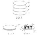
- FIG. 1shows an embodiment of an optical chassis 5 of the present invention having four substrates. These four substrates include a mount substrate 10 , a spacer substrate 20 , a sealer substrate 30 and an optional optics substrate 40 .
- the mount substrate 10serves as a mount for optoelectronic devices, here a light source 12 and a power monitor 14 , and provides the electrical interconnections, here including a wire bond 16 , conductive patterns 17 and metalized trenches 18 .
- the conductive patterns 17each include a pad for the wire bond 16 and connect the pad to the trench 18 for external communication.
- the conductive patterns 17may be created by patterning conductive material on the mount substrate 10 in a known manner.
- the trenches 18may be created by removing a portion of the mount substrate 10 in a conventional manner and filling this portion with conductive material.
- the conductive material for the trenches 18may be provided at the same time the conductive patterns 17 are formed.
- the details of the mount substrate 10can be seen more clearly in FIG. 2.
- the spacer substrate 20provides room for the beam output from the light source 12 to expand. If the optoelectronic device 12 does not have its active area on its top face, e.g., an edge emitting laser, an appropriate portion of a sidewall 22 of the spacer substrate 20 may be angled and coated with a reflective coating to appropriately direct the beam in the optical chassis 5 .
- a hole 24 in the spacer wafer 20may be formed by etching a silicon wafer, producing the characteristic angled sidewall 22 from such an etch.
- the spacer substrate 20in conjunction with the sealer substrate 30 , hermetically seals and protects the optoelectronic devices 12 , 14 from the environment.
- the sealer substrate 30may also include an optical element on either surface thereof, e.g., an optical element which reduces the divergence of the beam output from the light source 12 .
- the optional optics substrate 40includes at least one optical element.
- a diffractive optical element 44 on a first surface of the optics substrate 40directs some of the light from the light source 12 to the power monitor 14 , as disclosed, for example, in commonly assigned U.S. Pat. No. 6,314,223 entitled “Diffractive Vertical Cavity Surface Emitting Laser Power Monitor and System.”
- a coupling element 42 on a second surface of the optics substrate 40may couple the light between the optoelectronic device, here the light source 12 , and further applications, e.g., a fiber.
- more than one functionalitymay be incorporated into each optical element.
- a separation feature 32e.g., an indentation or stand off, may be provided on either the sealer substrate 30 or the optional optics substrate 40 to insure proper functioning of the optical element.
- the sealer substrate 30is transparent.
- the sealer substrate 30may be glass or may be some other transparent material that closely matches the coefficient of thermal expansion of the spacer substrate 20 , e.g., Pyrex when the spacer substrate is silicon.
- the smaller size of the chassis 5e.g., roughly 2 mm by 2 mm in x and y, also helps with any thermal mismatch, since there is not a lot of strain placed in the securing joints between the substrates.
- mating featuresmay be provided on a terminal surface thereof.
- a standoff 43encircling the optical element 42 may be provided.
- the standoff 43may be SU-8 and provides both alignment of the optical chassis 5 with additional devices and provides separation of the optical element 42 .
- a plurality of each of these substratesmay be created on a wafer level, secured together with other substrates in a vertical stack, and then vertically separated to form a plurality of individual optical chassis 5 .
- a mount wafer 10 ′, a spacer wafer 20 ′, a sealer wafer 30 ′ and an optional optics wafer 40 ′are to be aligned and secured together on a wafer level.
- Each of these wafersincludes a plurality of the respective mount substrates 10 , spacer substrates 20 , sealer substrates 30 and optional optical substrates 40 .
- the top three wafers 40 ′, 30 ′ and 20 ′may be created completely on a wafer level in known fashions. These wafers may then be secured together as shown in FIG. 4 forming a secured stack wafer 50 ′. These wafers may be aligned and secured as set forth, for example, in U.S. Pat. No. 6,096,155 entitled “Method of Dicing Wafer Level Integrated Optical Elements.”
- a plurality of metalized trenches 18 for providing the electrical interconnectionsmay be formed on the wafer level.
- the optoelectronic elements 12 , 14may then be positioned on the mount wafer 10 ′, e.g., using pick-and-place techniques, and then wire bonded 16 to the metalized trenches 18 .
- the metalized trenches 18may extend along the mount wafer 10 ′, so the separation of the mount wafer 10 ′ will expose the metal on the edge of the mount substrate, as can be seen in FIGS. 1 and 2.
- the secured stack wafer 50 ′is then secured to the mount wafer 10 ′ and then vertically separated to form a plurality of optical chassis 5 as shown in FIG. 1. Alternatively, the secured stack wafer may be vertically separated to form secured stack substrates, which are then bonded to the mount wafer 10 ′.
- the optional optical substrate 40is not included.
- Only a diffractive optical element 34 for power monitoring and/or efficient couplingis provided on the sealer substrate 30 .
- the spacer substrate 20is the same as in FIG. 1.
- the mount substrate 60provides different electrical connections as in FIG. 1 for the light source 12 and the power monitor 14 .
- the optoelectronic devicesare again wire bonded, here to conductive pads 65 .
- conductive, e.g., metalized, through holes or vias 64 and conductive structures 62e.g., solder balls, are used to provide the electrical interconnections to the optical elements on the top surface of the mount substrate 60 .
- FIGS. 8A-8DAnother alternative for providing electrical interconnections to the optoelectronic element on a wafer level is shown in FIGS. 8A-8D.
- a saw or other etching deviceis used to produce V-shaped groove 81 in a wafer 80 .
- the groove 81 and the wafer 80are coated with an electrically conductive coating 82 , e.g., metal, as shown in FIG. 8B.
- the wafer 80is separated at the V-groove 81 and at another portion to form a mount substrate 83 , as shown in FIG. 8C.
- the groove 81needs to be wide enough so that an angle remains after separation. For example, if dicing is used as the separation technique, the groove will need to be wider than the blade width of the dicing saw.
- an optoelectronic device 86is mounted on the conductive coating 82 of the mount substrate 83 .
- a solder ball 84 or other conductive structuremay then used to connect the conductive coating 82 to an electrical connection on a board 88 .
- the other substrates 20 , 30 and optionally 40may be stacked over the mount substrate 83 as shown in the other configurations.
- Electrical input/outputmay also be realized as shown in FIG. 9, in which the substrates forming the optical chassis do not have the same width, thereby forming a ledge 15 , with the electrical connection being realized on a portion of the chassis 5 providing the ledge 15 .
- the ledge 15may be formed by having the mount substrate 10 extend further in at least one direction than the adjacent spacer substrate 20 .
- the electrical contactsmay be formed on the surface of the ledge or a portion of the ledge 15 may be removed to form the trenches 18 therein to increase the surface for electrical contact.
- Such a ledgemay be formed by die bonding a secured stacked substrate having the spacer substrate 20 and the sealer substrate 30 to the mount substrate 10 .
- Forming such a ledge on wafer levelmay be realized in a number of manners, including using dicing saws of different thicknesses and dicing through opposite surfaces, e.g., flipping the wafer after partial dicing, of the secured stacked wafer, including the mount wafer 10 ′. Details of forming such a ledge on a wafer level are set forth in the commonly assigned, co-pending application entitled “Separating of Optical Integrated Modules and Structures Formed Thereby,” filed Oct. 23, 2001, which is hereby incorporated by reference in its entirety.
- the optical chassis of the present inventionmay be used to simply replace the conventional TO-can element and can have the conventional optics aligned thereto, as is currently done for the TO-can optoelectronics. Two manners of achieving this are shown in shown in FIGS. 10 and 11.
- the vertically integrated optical chassis 55 of the present inventionmay have an optical element 90 , including optical elements larger in the x- and/or y-direction than the optical chassis 55 , die-bonded thereto.
- the optical element 90may be separate from but aligned with the optical chassis 55 , here shown in a common housing 92 . This separation reduces the alignment tolerances for the optical element 90 .
- the sealer substrate 30may still include optics thereon for improving the light from the light source 12 , e.g., collimating or at least reducing the divergence of the light.
- FIGS. 12A-12BA specific configuration of an optical chassis in accordance with the present invention is shown in FIGS. 12A-12B.
- an optical chassis 100is attached to a flex lead 150 , inserted into a magnet 160 , on which a fiber stop 170 and then a fiber sleeve 180 is secured.
- This structuremay be provided on a heat sink.
- the optical chassis 100includes a mount substrate 110 having a ledge 115 , a spacer substrate 120 and a sealer substrate 130 .
- An optoelectronic device 112 and wire bonds 116are on the mount substrate 110 .
- the sealer substrate 130includes a lens 132 and an angled, reflective sidewall 122 .
- the angled, reflective sidewall 122serves as a mirror to direct light between the optoelectronic device 112 and the fiber in the fiber sleeve 180 . If the active area or facet of the optoelectronic device is not on an edge thereof, this angled, reflective sidewall 122 is not needed.
- An additional spacer substrate 136which may include additional spacing structures 138 , separates the lens 132 from an isolator stack 140 .
- the spacing structures 138are used when a passive optical element is on one or more opposing surfaces in the stack and the surfaces would otherwise by flush at the passive optical element.
- the spacing structuresmay be integral with the surface or may be provided on the surface. Alternatively, these spacing structures may be on the sealer substrate 130 .
- the electrical connection of the optoelectronic device 116is realized using the ledge 115 , as discussed in connection with FIG. 9.
- the isolator stack 140includes a first polarizer 142 , a Faraday rotator 144 and a second polarizer 146 .
- the magnet 170which may be a ring magnet, surrounds the isolator stack 140 when the optical chassis 100 is inserted as shown in FIG. 12A, thereby completing the isolator. If the Faraday rotator 144 is a latching type, then the speared magnet 170 is not needed.
- the active elementsare secured to the mount substrate such that they remain secured and withstand subsequent processing, e.g., the securing of the substrate.
- the construction of the optical chassis of the present inventionneeds to be determined in an appropriate order, with the least robust technique being performed last.
- the materials used for the securing of the active elements, realizing the electrical connections and the securing of the substratesmust be selected in accordance with the required order.
- the active elementsmay be secured on the mount substrate using a gold-tin (AuSn) solder and the substrates may then be secured using a material with a lower melting point, e.g., silver-tin (AgSn) solder.
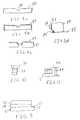
- FIGS. 13A-14BTechniques for realizing alignment of the optical elements in the optical chassis are shown in FIGS. 13A-14B.
- characteristicse.g., lens thickness, radius of curvature (ROC), of individual elements.
- ROCradius of curvature
- the variation in ROCmay be compensated for with the placement of the angled surface 122 of the spacer substrate 120 , as shown in FIG. 13A-13B.
- the separation d between the optoelectronic device 112 and a back edge of the angled surface 122is determined in accordance with the ROC of the lens to be used. If the angled surface 122 has an angle of approximately 45°, this distance d will be roughly equal to the height of the spacer substrate 120 . Thus, this aligning of the optoelectronic device 112 with the angled surface 122 compensates for any variations in the thickness of the spacer substrate 120 , as well as taking the ROC of the lens into account.
- FIGS. 14A-14BThe aligning of the lens to the optoelectronic device 112 is shown in FIGS. 14A-14B.
- the image of the active area of the optoelectronic device 112 in the reflective angled surface 122may be used to align the lens.
- a bottom surface of the substrate having the lens thereonwhich may be the sealer substrate 130 as shown in FIGS. 12A-12B, includes alignment features 134 , here in the form of a crosshair centered on the lens on the top surface of the substrate.
- the alignment features 134are then centered with the image of the active area of the optoelectronic device 112 as reflected by the angled surface 122 to insure proper alignment there between. Since the height of the optoelectronic element changes its location on the angled surface 122 , by aligning the lens to the reflection from the angled surface 122 , variations in the height of the optoelectronic element may be compensated for as well.
- the lensmay be aligned by directly viewing the active area using alignment features 134 .
- the alignment thereofis not critical. Since the sealer substrate 130 is transparent, alignment features do not need to be provided thereon, as alignment features on surfaces below the sealer substrate may be viewed through it. If there are optical elements on other substrates, and the sealer substrate 130 is transparent, the same alignment techniques may be employed.
- an optical chassis having a small form factormay be created at least partially on a wafer level, including electrical interconnections.
- the optical chassis of the present inventionalso provides a hermetic seal without requiring a TO can or other separate housing. Further, since substrates of the optical chassis are secured to one another, rather than to a carrier as in a TO can, better alignment can be maintained for longer.
- any of the electrical interconnections shownmay be used with any optical chassis embodiments.
- additional optical substrates or elements as neededmay be secured to the optical chassis.
- any of the configurations of the optical chassismay be created at least partially on a wafer level as discussed regarding FIGS. 3-5.
Landscapes
- Physics & Mathematics (AREA)
- General Physics & Mathematics (AREA)
- Optics & Photonics (AREA)
- Condensed Matter Physics & Semiconductors (AREA)
- Electromagnetism (AREA)
- Led Device Packages (AREA)
- Optical Couplings Of Light Guides (AREA)
Abstract
Description
- The present application claims priority under 35 U.S.C. §119 to U.S. Provisional Application Ser. No. 60/457,664 filed on Mar. 26, 2003, entitled “Wafer Based Optical Chassis” and under 35[0001]
U.S.C. § 120 as a continuation-in-part to U.S. application Ser. No. 09/983,278 filed Oct. 23, 2001, entitled “Separating of Optical Integrated Modules and Structures Formed Thereby,” the entire contents of both of which are hereby incorporated by reference for all purposes. - 1. Field of the Invention[0002]
- The present invention is directed to a wafer based optical chassis and associated methods. More particularly, the present invention is directed to protecting active elements in an optical system and realizing electrical input/output without requiring separate packaging.[0003]
- 2. Description of Related Art[0004]
- Active elements, such as optoelectronic chips, e.g., light sources for transmitters and detectors for receivers, are typically housed in a transistor outline (TO) can. Such a TO can is typically made of metal, has a large form factor, involves an expensive serial manufacturing process and requires active alignment with external passive optical elements. This large form factor separates the active element from an external passive optic along the optical axis, resulting in the passive optic needing to handle a more divergent beam, rendering the optic bigger, thereby further increasing the size of the system. Additionally, the TO can has electrical termination concerns, limiting the speed of the active elements.[0005]
- Current trends towards miniaturization have spurred numerous small form factor designs. Most of these designs are directed to integrating the passive optical element with some connector, separate from the TO can. While this may reduce the length of the system and simplify the manufacturing of the passive optical portion of the system, the TO can, and the problems attendant therewith, are still present.[0006]
- The present invention is therefore directed to a wafer based optical chassis and associated methods that substantially overcome one or more of the problems due to the limitations and disadvantages of the related art.[0007]
- It is a feature of the present invention to protect an active element with an assembly including passive optical elements. It is another feature of the present invention to provide efficient electrical coupling to and from the protected active elements. It is yet another feature of the present invention to provide hermetic packaging of an active element that can at least partially be created in parallel. It is yet another feature of the present invention to provide alignment that compensates for variations arising in the manufacturing process.[0008]
- At least one of the above and other features may be realized by providing an optical apparatus including a mount substrate, an optoelectronic device on the mount substrate, a spacer substrate and a sealer substrate. The mount substrate, the spacer substrate and the sealer substrate are vertically stacked and hermetically seal the optoelectronic device. The apparatus also includes external electrical contact for the optoelectronic device outside the sealing.[0009]
- An interior surface of the spacer substrate may be angled and have a reflective material thereon. The electrical contact may include a metalized trench. The mount substrate and the spacer substrate may be flush. The optical apparatus as may include a ledge formed by differing widths between the mount substrate and the spacer substrate. The metalized trenches may be in the ledge or the electrical contact may be on the ledge. The electrical contact may include a conductive via on a bottom surface of the mount substrate and a conductive structure in the via. The conductive structure is a solder ball. The electrical contact may include a conductive material on at least two non-parallel surfaces of the mount substrate.[0010]
- A passive optical element may be on a surface of the sealer substrate. The optical apparatus may include, above the sealer substrate, an optical block having a passive optical element on at least one surface thereof. The optical apparatus may include, above the sealer substrate, an isolator stack including first and second polarizers and a Faraday rotator sandwiched between the first and second polarizers. The optical apparatus may include, above the sealer substrate, another spacer substrate. At least two of the mount substrate, the spacer substrate and the sealer substrate are of materials with approximately same coefficients of thermal expansion. One of the at least two substrates may be silicon and the other may be Pyrex. A terminal surface of the optical apparatus may include a mating feature for mating the optical apparatus with another structure, e.g., a ferrule.[0011]
- At least one of the above and other features may be realized by providing a method of aligning an active device and a lens, including providing the active device on a mount substrate, the active device having an active area on a side thereof, positioning an angled reflector relative to the active area in accordance with a radius of curvature of the lens, viewing the active area reflected by the angled reflector, and positioning the lens in accordance with the viewed active area.[0012]
- At least one of the above and other features may be realized by providing a method of creating a plurality of optical apparatuses, including patterning a conductive material on a mount wafer, populating the mount substrate with optoelectronic devices in accordance with the patterning, stacking and securing a spacer substrate on the mount wafer, stacking and securing a sealer substrate on the spacer substrate, wherein the stacking and securing of the spacer substrate and the sealer substrate on the mount wafer hermetically seal the optoelectronic devices, and vertically separating the mount wafer to form the plurality of optical apparatuses. The vertically separating including exposing a portion of the conductive material outside the hermetic seal. Each optical apparatus includes a mount substrate, an optoelectronic device, a spacer substrate, a sealer substrate, and exposed conductive material.[0013]
- The stacking and securing of the sealer substrate to the spacer substrate occurs before stacking and securing of the spacer substrate stacked to the mount substrate.[0014]
- The above and other features and advantages of the present invention will become readily apparent to those of skill in the art by describing in detail embodiments thereof with reference to the attached drawings, in which:[0015]
- FIG. 1 is an elevational perspective view of an embodiment of the optical chassis of the present invention;[0016]
- FIG. 2 is a detailed elevational perspective view of the optoelectronic devices and electrical interconnections of the optical chassis of FIG. 1;[0017]
- FIG. 3 is an elevational perspective exploded view of the wafer components to be used to create the optical chassis of FIG. 1;[0018]
- FIG. 4 is an elevational perspective view of the passive optical element wafers of FIG. 3 secured together;[0019]
- FIG. 5 is an elevational perspective view of the active element wafer to be bonded to the stack of wafers in FIG. 4 and then vertically separated to form the optical chassis of FIG. 1;[0020]
- FIG. 6 an elevational perspective view of another embodiment of the optical chassis of the present invention;[0021]
- FIG. 7 is a detailed perspective bottom view of the electrical interconnections of the optical chassis shown in FIG. 6;[0022]
- FIGS. 8[0023]a-8dare schematic drawings illustrating creation and use of an electrical connection on the face of a substrate;
- FIG. 9 is a schematic side view of another embodiment of electrical connections for the optical chassis;[0024]
- FIG. 10 is a schematic side view of the optical chassis with a larger optical element bonded thereto:[0025]
- FIG. 11 is a schematic side view of the optical chassis in a common housing with a larger optical element;[0026]
- FIG. 12A is a schematic cross-section of a specific configuration of the optical chassis of the present invention inserted in a system;[0027]
- FIG. 12B is a schematic cross-section of the specific configuration of the optical chassis of FIG. 12A alone;[0028]
- FIG. 13A is a schematic top view of alignment of the active optical element to the mirror;[0029]
- FIG. 13B is a schematic side view of alignment of the active optical element to the mirror;[0030]
- FIG. 14A is a schematic top view of alignment of the active optical element to the optics block; and[0031]
- FIG. 14B is a schematic bottom view of alignment features of the optics block.[0032]
- The present invention will now be described more fully hereinafter with reference to the accompanying drawings, in which exemplary embodiments of the invention are shown. The invention may, however, be embodied in different forms and should not be construed as limited to the embodiments set forth herein. Rather, these embodiments are provided so that this disclosure will be thorough and complete, and will fully convey the concept of the invention to those skilled in the art. In the drawings, the thickness of layers and regions are exaggerated for clarity. It will also be understood that when a layer is referred to as being “on” another layer or substrate, it may be directly on the other layer or substrate, or intervening layers may also be present. Further, it will be understood that when a layer is referred to as being “under” another layer, it may be directly under, or one or more intervening layers may also be present. In addition, it will also be understood that when a layer is referred to as being “between” two layers, it may be the only layer between the two layers, or one or more intervening layers may also be present. Like numbers refer to like elements throughout.[0033]
- FIG. 1 shows an embodiment of an[0034]
optical chassis 5 of the present invention having four substrates. These four substrates include amount substrate 10, aspacer substrate 20, asealer substrate 30 and anoptional optics substrate 40. Themount substrate 10 serves as a mount for optoelectronic devices, here alight source 12 and apower monitor 14, and provides the electrical interconnections, here including awire bond 16, conductive patterns17 and metalizedtrenches 18. The conductive patterns17 each include a pad for thewire bond 16 and connect the pad to thetrench 18 for external communication. The conductive patterns17 may be created by patterning conductive material on themount substrate 10 in a known manner. Thetrenches 18 may be created by removing a portion of themount substrate 10 in a conventional manner and filling this portion with conductive material. The conductive material for thetrenches 18 may be provided at the same time the conductive patterns17 are formed. The details of themount substrate 10 can be seen more clearly in FIG. 2. - The[0035]
spacer substrate 20 provides room for the beam output from thelight source 12 to expand. If theoptoelectronic device 12 does not have its active area on its top face, e.g., an edge emitting laser, an appropriate portion of asidewall 22 of thespacer substrate 20 may be angled and coated with a reflective coating to appropriately direct the beam in theoptical chassis 5. Ahole 24 in thespacer wafer 20 may be formed by etching a silicon wafer, producing the characteristicangled sidewall 22 from such an etch. Thespacer substrate 20, in conjunction with thesealer substrate 30, hermetically seals and protects theoptoelectronic devices sealer substrate 30 may also include an optical element on either surface thereof, e.g., an optical element which reduces the divergence of the beam output from thelight source 12. - The[0036]
optional optics substrate 40 includes at least one optical element. Here, a diffractiveoptical element 44 on a first surface of theoptics substrate 40 directs some of the light from thelight source 12 to thepower monitor 14, as disclosed, for example, in commonly assigned U.S. Pat. No. 6,314,223 entitled “Diffractive Vertical Cavity Surface Emitting Laser Power Monitor and System.” Acoupling element 42 on a second surface of theoptics substrate 40 may couple the light between the optoelectronic device, here thelight source 12, and further applications, e.g., a fiber. Of course, more than one functionality may be incorporated into each optical element. - If an optical element is to be provided on one or both of the surfaces of the optional[0037]
optical substrate 40 or thesealer substrate 30 adjacent to one another, aseparation feature 32, e.g., an indentation or stand off, may be provided on either thesealer substrate 30 or theoptional optics substrate 40 to insure proper functioning of the optical element. Thesealer substrate 30 is transparent. Thesealer substrate 30 may be glass or may be some other transparent material that closely matches the coefficient of thermal expansion of thespacer substrate 20, e.g., Pyrex when the spacer substrate is silicon. The smaller size of thechassis 5, e.g., roughly 2 mm by 2 mm in x and y, also helps with any thermal mismatch, since there is not a lot of strain placed in the securing joints between the substrates. - Finally, when the[0038]
optical chassis 5 is to be joined with another device, mating features may be provided on a terminal surface thereof. For example, if the optical chassis is to be mated with a fiber optic ferule, astandoff 43 encircling theoptical element 42 may be provided. Thestandoff 43 may be SU-8 and provides both alignment of theoptical chassis 5 with additional devices and provides separation of theoptical element 42. - As can be seen from the profile of the[0039]
optical chassis 5, a plurality of each of these substrates may be created on a wafer level, secured together with other substrates in a vertical stack, and then vertically separated to form a plurality of individualoptical chassis 5. As shown in FIG. 3, amount wafer 10′, aspacer wafer 20′, asealer wafer 30′ and anoptional optics wafer 40′ are to be aligned and secured together on a wafer level. Each of these wafers includes a plurality of therespective mount substrates 10,spacer substrates 20,sealer substrates 30 and optionaloptical substrates 40. The top threewafers 40′,30′ and20′ may be created completely on a wafer level in known fashions. These wafers may then be secured together as shown in FIG. 4 forming a secured stack wafer50′. These wafers may be aligned and secured as set forth, for example, in U.S. Pat. No. 6,096,155 entitled “Method of Dicing Wafer Level Integrated Optical Elements.” - For the[0040]
mount wafer 10′, a plurality of metalizedtrenches 18 for providing the electrical interconnections may be formed on the wafer level. Theoptoelectronic elements mount wafer 10′, e.g., using pick-and-place techniques, and then wire bonded16 to the metalizedtrenches 18. The metalizedtrenches 18 may extend along themount wafer 10′, so the separation of themount wafer 10′ will expose the metal on the edge of the mount substrate, as can be seen in FIGS. 1 and 2. The secured stack wafer50′ is then secured to themount wafer 10′ and then vertically separated to form a plurality ofoptical chassis 5 as shown in FIG. 1. Alternatively, the secured stack wafer may be vertically separated to form secured stack substrates, which are then bonded to themount wafer 10′. - An alternative[0041]
optical chassis 55 is shown in FIGS. 6 and 7. Here, the optionaloptical substrate 40 is not included. Only a diffractiveoptical element 34 for power monitoring and/or efficient coupling is provided on thesealer substrate 30. Thespacer substrate 20 is the same as in FIG. 1. Themount substrate 60 provides different electrical connections as in FIG. 1 for thelight source 12 and thepower monitor 14. Here, the optoelectronic devices are again wire bonded, here to conductive pads65. Then, on the bottom of themount substrate 60, conductive, e.g., metalized, through holes orvias 64 andconductive structures 62, e.g., solder balls, are used to provide the electrical interconnections to the optical elements on the top surface of themount substrate 60. These conductive structures must be large enough to obscure the hole in the mount substrate to insure the hermetic seal, to avoid creating a thermal gradient and to avoid extra oxidation. This solution is particularly useful if the mount substrate is a ceramic, since it is expensive to put solder on ceramic. - Another alternative for providing electrical interconnections to the optoelectronic element on a wafer level is shown in FIGS. 8A-8D. As shown in FIG. 8A, a saw or other etching device is used to produce V-shaped groove[0042]81 in a
wafer 80. Then, the groove81 and thewafer 80 are coated with an electricallyconductive coating 82, e.g., metal, as shown in FIG. 8B. Then, thewafer 80 is separated at the V-groove81 and at another portion to form amount substrate 83, as shown in FIG. 8C. The groove81 needs to be wide enough so that an angle remains after separation. For example, if dicing is used as the separation technique, the groove will need to be wider than the blade width of the dicing saw. - As shown in FIG. 8D, an optoelectronic device[0043]86 is mounted on the
conductive coating 82 of themount substrate 83. Asolder ball 84 or other conductive structure may then used to connect theconductive coating 82 to an electrical connection on aboard 88. Theother substrates mount substrate 83 as shown in the other configurations. - Electrical input/output may also be realized as shown in FIG. 9, in which the substrates forming the optical chassis do not have the same width, thereby forming a[0044]
ledge 15, with the electrical connection being realized on a portion of thechassis 5 providing theledge 15. As shown in FIG. 9, theledge 15 may be formed by having themount substrate 10 extend further in at least one direction than theadjacent spacer substrate 20. The electrical contacts may be formed on the surface of the ledge or a portion of theledge 15 may be removed to form thetrenches 18 therein to increase the surface for electrical contact. - Such a ledge may be formed by die bonding a secured stacked substrate having the[0045]
spacer substrate 20 and thesealer substrate 30 to themount substrate 10. Forming such a ledge on wafer level may be realized in a number of manners, including using dicing saws of different thicknesses and dicing through opposite surfaces, e.g., flipping the wafer after partial dicing, of the secured stacked wafer, including themount wafer 10′. Details of forming such a ledge on a wafer level are set forth in the commonly assigned, co-pending application entitled “Separating of Optical Integrated Modules and Structures Formed Thereby,” filed Oct. 23, 2001, which is hereby incorporated by reference in its entirety. - If customized performance of the optical chassis is known, optional optical substrate(s) may be incorporated to provide the desired performance. Otherwise, the optical chassis of the present invention may be used to simply replace the conventional TO-can element and can have the conventional optics aligned thereto, as is currently done for the TO-can optoelectronics. Two manners of achieving this are shown in shown in FIGS. 10 and 11. As shown in FIG. 10, the vertically integrated[0046]
optical chassis 55 of the present invention may have anoptical element 90, including optical elements larger in the x- and/or y-direction than theoptical chassis 55, die-bonded thereto. As shown in FIG. 11, theoptical element 90 may be separate from but aligned with theoptical chassis 55, here shown in acommon housing 92. This separation reduces the alignment tolerances for theoptical element 90. Thesealer substrate 30 may still include optics thereon for improving the light from thelight source 12, e.g., collimating or at least reducing the divergence of the light. - A specific configuration of an optical chassis in accordance with the present invention is shown in FIGS. 12A-12B. As can be seen therein, an[0047]
optical chassis 100 is attached to a flex lead150, inserted into amagnet 160, on which a fiber stop170 and then afiber sleeve 180 is secured. This structure may be provided on a heat sink. - The[0048]
optical chassis 100 includes amount substrate 110 having aledge 115, aspacer substrate 120 and asealer substrate 130. Anoptoelectronic device 112 andwire bonds 116 are on themount substrate 110. Thesealer substrate 130 includes a lens132 and an angled,reflective sidewall 122. The angled,reflective sidewall 122 serves as a mirror to direct light between theoptoelectronic device 112 and the fiber in thefiber sleeve 180. If the active area or facet of the optoelectronic device is not on an edge thereof, this angled,reflective sidewall 122 is not needed. - An[0049]
additional spacer substrate 136, which may includeadditional spacing structures 138, separates the lens132 from anisolator stack 140. The spacingstructures 138 are used when a passive optical element is on one or more opposing surfaces in the stack and the surfaces would otherwise by flush at the passive optical element. The spacing structures may be integral with the surface or may be provided on the surface. Alternatively, these spacing structures may be on thesealer substrate 130. The electrical connection of theoptoelectronic device 116 is realized using theledge 115, as discussed in connection with FIG. 9. - The[0050]
isolator stack 140 includes afirst polarizer 142, aFaraday rotator 144 and asecond polarizer 146. The magnet170, which may be a ring magnet, surrounds theisolator stack 140 when theoptical chassis 100 is inserted as shown in FIG. 12A, thereby completing the isolator. If theFaraday rotator 144 is a latching type, then the speared magnet170 is not needed. - In any of the above configurations, the active elements are secured to the mount substrate such that they remain secured and withstand subsequent processing, e.g., the securing of the substrate. The construction of the optical chassis of the present invention needs to be determined in an appropriate order, with the least robust technique being performed last. The materials used for the securing of the active elements, realizing the electrical connections and the securing of the substrates must be selected in accordance with the required order. For example, the active elements may be secured on the mount substrate using a gold-tin (AuSn) solder and the substrates may then be secured using a material with a lower melting point, e.g., silver-tin (AgSn) solder.[0051]
- Techniques for realizing alignment of the optical elements in the optical chassis are shown in FIGS. 13A-14B. In making micro-optical elements, there are inevitable variations in characteristics, e.g., lens thickness, radius of curvature (ROC), of individual elements. By classifying these lenses by their ROC into different groups within a range, e.g., ±1%, the variation in ROC may be compensated for with the placement of the[0052]
angled surface 122 of thespacer substrate 120, as shown in FIG. 13A-13B. Once a lens is selected for a particularoptoelectronic device 112 on themount substrate 110, the separation d between theoptoelectronic device 112 and a back edge of theangled surface 122 is determined in accordance with the ROC of the lens to be used. If theangled surface 122 has an angle of approximately 45°, this distance d will be roughly equal to the height of thespacer substrate 120. Thus, this aligning of theoptoelectronic device 112 with theangled surface 122 compensates for any variations in the thickness of thespacer substrate 120, as well as taking the ROC of the lens into account. - The aligning of the lens to the[0053]
optoelectronic device 112 is shown in FIGS. 14A-14B. Here, the image of the active area of theoptoelectronic device 112 in the reflectiveangled surface 122 may be used to align the lens. A bottom surface of the substrate having the lens thereon, which may be thesealer substrate 130 as shown in FIGS. 12A-12B, includes alignment features134, here in the form of a crosshair centered on the lens on the top surface of the substrate. The alignment features134 are then centered with the image of the active area of theoptoelectronic device 112 as reflected by theangled surface 122 to insure proper alignment there between. Since the height of the optoelectronic element changes its location on theangled surface 122, by aligning the lens to the reflection from theangled surface 122, variations in the height of the optoelectronic element may be compensated for as well. - If the active area of the[0054]
optoelectronic device 112 is not on a side thereof, the lens may be aligned by directly viewing the active area using alignment features134. The variation in height of such optoelectronic devices, i.e., in the z-direction, do not significantly affect the performance. If there are no optical elements on thesealer substrate 130, the alignment thereof is not critical. Since thesealer substrate 130 is transparent, alignment features do not need to be provided thereon, as alignment features on surfaces below the sealer substrate may be viewed through it. If there are optical elements on other substrates, and thesealer substrate 130 is transparent, the same alignment techniques may be employed. - Thus, in accordance with the present invention, an optical chassis having a small form factor may be created at least partially on a wafer level, including electrical interconnections. The optical chassis of the present invention also provides a hermetic seal without requiring a TO can or other separate housing. Further, since substrates of the optical chassis are secured to one another, rather than to a carrier as in a TO can, better alignment can be maintained for longer.[0055]
- While the present invention is described herein with reference to illustrative embodiments for particular applications, it should be understood that the present invention is not limited thereto. Those having ordinary skill in the art and access to the teachings provided herein will recognize additional modifications, applications, and embodiments within the scope thereof and additional fields in which the invention would be of significant utility without undue experimentation. For example, any of the electrical interconnections shown may be used with any optical chassis embodiments. Further, additional optical substrates or elements as needed may be secured to the optical chassis. Finally, any of the configurations of the optical chassis may be created at least partially on a wafer level as discussed regarding FIGS. 3-5.[0056]
Claims (20)
Priority Applications (4)
| Application Number | Priority Date | Filing Date | Title |
|---|---|---|---|
| US10/809,914US7224856B2 (en) | 2001-10-23 | 2004-03-26 | Wafer based optical chassis and associated methods |
| US11/783,530US7751659B2 (en) | 2001-10-23 | 2007-04-10 | Optical apparatus |
| US11/932,693US7961989B2 (en) | 2001-10-23 | 2007-10-31 | Optical chassis, camera having an optical chassis, and associated methods |
| US12/801,940US8233757B2 (en) | 2001-10-23 | 2010-07-02 | Wafer based optical chassis and associated methods |
Applications Claiming Priority (3)
| Application Number | Priority Date | Filing Date | Title |
|---|---|---|---|
| US09/983,278US6798931B2 (en) | 2001-03-06 | 2001-10-23 | Separating of optical integrated modules and structures formed thereby |
| US45766403P | 2003-03-26 | 2003-03-26 | |
| US10/809,914US7224856B2 (en) | 2001-10-23 | 2004-03-26 | Wafer based optical chassis and associated methods |
Related Parent Applications (1)
| Application Number | Title | Priority Date | Filing Date |
|---|---|---|---|
| US09/983,278Continuation-In-PartUS6798931B2 (en) | 2001-03-06 | 2001-10-23 | Separating of optical integrated modules and structures formed thereby |
Related Child Applications (1)
| Application Number | Title | Priority Date | Filing Date |
|---|---|---|---|
| US11/783,530ContinuationUS7751659B2 (en) | 2001-10-23 | 2007-04-10 | Optical apparatus |
Publications (2)
| Publication Number | Publication Date |
|---|---|
| US20040247232A1true US20040247232A1 (en) | 2004-12-09 |
| US7224856B2 US7224856B2 (en) | 2007-05-29 |
Family
ID=38367516
Family Applications (3)
| Application Number | Title | Priority Date | Filing Date |
|---|---|---|---|
| US10/809,914Expired - LifetimeUS7224856B2 (en) | 2001-10-23 | 2004-03-26 | Wafer based optical chassis and associated methods |
| US11/783,530Expired - Fee RelatedUS7751659B2 (en) | 2001-10-23 | 2007-04-10 | Optical apparatus |
| US12/801,940Expired - Fee RelatedUS8233757B2 (en) | 2001-10-23 | 2010-07-02 | Wafer based optical chassis and associated methods |
Family Applications After (2)
| Application Number | Title | Priority Date | Filing Date |
|---|---|---|---|
| US11/783,530Expired - Fee RelatedUS7751659B2 (en) | 2001-10-23 | 2007-04-10 | Optical apparatus |
| US12/801,940Expired - Fee RelatedUS8233757B2 (en) | 2001-10-23 | 2010-07-02 | Wafer based optical chassis and associated methods |
Country Status (1)
| Country | Link |
|---|---|
| US (3) | US7224856B2 (en) |
Cited By (5)
| Publication number | Priority date | Publication date | Assignee | Title |
|---|---|---|---|---|
| JP2011107705A (en)* | 2009-11-16 | 2011-06-02 | Tessera North America Inc | Triplexer for optical fiber, package including the same and associated method |
| US20120063718A1 (en)* | 2010-09-13 | 2012-03-15 | Tyco Electronics Svenska Holdings Ab | Miniaturized high speed optical module |
| US20140361200A1 (en)* | 2011-12-22 | 2014-12-11 | Heptagon Micro Optics Pte. Ltd. | Opto-Electronic Modules, In Particular Flash Modules, and Method For Manufacturing The Same |
| US20170153128A1 (en)* | 2012-07-17 | 2017-06-01 | Heptagon Micro Optics Pte. Ltd. | Sensor module and method of manufacturing the same |
| CN115064599A (en)* | 2022-06-10 | 2022-09-16 | 无锡泓瑞航天科技有限公司 | Preparation method of metal film layer of metallized window sheet for infrared detector |
Families Citing this family (18)
| Publication number | Priority date | Publication date | Assignee | Title |
|---|---|---|---|---|
| US20050255722A1 (en)* | 2004-05-07 | 2005-11-17 | Salmon Peter C | Micro blade assembly |
| US7427809B2 (en)* | 2004-12-16 | 2008-09-23 | Salmon Technologies, Llc | Repairable three-dimensional semiconductor subsystem |
| US20070007983A1 (en)* | 2005-01-06 | 2007-01-11 | Salmon Peter C | Semiconductor wafer tester |
| US20070023889A1 (en)* | 2005-08-01 | 2007-02-01 | Salmon Peter C | Copper substrate with feedthroughs and interconnection circuits |
| US7586747B2 (en)* | 2005-08-01 | 2009-09-08 | Salmon Technologies, Llc. | Scalable subsystem architecture having integrated cooling channels |
| US20070023923A1 (en)* | 2005-08-01 | 2007-02-01 | Salmon Peter C | Flip chip interface including a mixed array of heat bumps and signal bumps |
| US20070023904A1 (en)* | 2005-08-01 | 2007-02-01 | Salmon Peter C | Electro-optic interconnection apparatus and method |
| KR20090033070A (en)* | 2007-09-27 | 2009-04-01 | 엘지이노텍 주식회사 | Camera module |
| TWI402979B (en)* | 2007-12-13 | 2013-07-21 | Sharp Kk | Electronic component wafer module, electronic component module, sensor wafer module, sensor module, lens array disk, sensor module manufacturing method, and electronic information device |
| FR2931587B1 (en)* | 2008-05-21 | 2011-05-13 | Commissariat Energie Atomique | METHOD FOR PRODUCING AN OPTICAL DEVICE WITH INTEGRATED OPTOELECTRONIC COMPONENTS |
| US20090321861A1 (en)* | 2008-06-26 | 2009-12-31 | Micron Technology, Inc. | Microelectronic imagers with stacked lens assemblies and processes for wafer-level packaging of microelectronic imagers |
| WO2010022503A1 (en)* | 2008-09-01 | 2010-03-04 | Lensvector Inc. | Wafer-level fabrication of liquid crystal optoelectronic devices |
| DE102009042479A1 (en) | 2009-09-24 | 2011-03-31 | Msg Lithoglas Ag | Method for producing an arrangement having a component on a carrier substrate and arrangement, and method for producing a semifinished product and semifinished product |
| JP2013000359A (en)* | 2011-06-16 | 2013-01-07 | Toshiba Corp | Endoscope apparatus and electronic apparatus |
| US9182545B2 (en)* | 2012-10-25 | 2015-11-10 | Empire Technology Development Llc | Wafer level optical device |
| US9563028B2 (en)* | 2013-01-31 | 2017-02-07 | Ccs Technology, Inc. | Method to manufacture an optoelectronic assembly |
| EP3125008A1 (en)* | 2015-07-29 | 2017-02-01 | CCS Technology Inc. | Method to manufacture optoelectronic modules |
| US9876200B2 (en) | 2015-08-07 | 2018-01-23 | International Business Machines Corporation | All-silicon hermetic package and processing for narrow, low-profile microbatteries |
Citations (12)
| Publication number | Priority date | Publication date | Assignee | Title |
|---|---|---|---|---|
| US126940A (en)* | 1872-05-21 | Improvement in hydraulic betons | ||
| US4873566A (en)* | 1985-10-28 | 1989-10-10 | American Telephone And Telegraph Company | Multilayer ceramic laser package |
| US4945400A (en)* | 1988-03-03 | 1990-07-31 | At&T Bell Laboratories | Subassembly for optoelectronic devices |
| US6104690A (en)* | 1996-09-27 | 2000-08-15 | Digital Optics Corporation | Integrated optical apparatus and associated methods |
| US6184066B1 (en)* | 1997-05-28 | 2001-02-06 | Matsushita Electric Industrial Co., Ltd. | Method for fabricating semiconductor device |
| US20020068373A1 (en)* | 2000-02-16 | 2002-06-06 | Nova Crystals, Inc. | Method for fabricating light emitting diodes |
| US20030002809A1 (en)* | 1998-06-08 | 2003-01-02 | Jian Benjamin B. | Vertically integrated optical devices coupled to optical fibers |
| US6509807B1 (en)* | 1997-04-08 | 2003-01-21 | X2Y Attenuators, Llc | Energy conditioning circuit assembly |
| US6581279B1 (en)* | 1998-08-25 | 2003-06-24 | Commissariat A L'energie Atomique | Method of collectively packaging electronic components |
| US6597713B2 (en)* | 1998-07-22 | 2003-07-22 | Canon Kabushiki Kaisha | Apparatus with an optical functional device having a special wiring electrode and method for fabricating the same |
| US6606011B2 (en)* | 1998-04-07 | 2003-08-12 | X2Y Attenuators, Llc | Energy conditioning circuit assembly |
| US20030162214A1 (en)* | 1993-11-01 | 2003-08-28 | Nanogen, Inc. | Self-addressable self-assembling microelectronic systems and devices for molecular biological analysis and diagnostics |
Family Cites Families (53)
| Publication number | Priority date | Publication date | Assignee | Title |
|---|---|---|---|---|
| US5011256A (en) | 1988-10-28 | 1991-04-30 | E. I. Du Pont De Nemours And Company | Package for an opto-electronic component |
| US4995695A (en) | 1989-08-17 | 1991-02-26 | At&T Bell Laboratories | Optical assembly comprising optical fiber coupling means |
| US5300788A (en)* | 1991-01-18 | 1994-04-05 | Kopin Corporation | Light emitting diode bars and arrays and method of making same |
| US5168537A (en) | 1991-06-28 | 1992-12-01 | Digital Equipment Corporation | Method and apparatus for coupling light between an optoelectronic device and a waveguide |
| US5359208A (en) | 1993-02-26 | 1994-10-25 | Nippon Sheet Glass Co., Ltd. | Chip package with microlens array |
| US5406543A (en)* | 1993-04-07 | 1995-04-11 | Olympus Optical Co., Ltd. | Optical head with semiconductor laser |
| US6059188A (en)* | 1993-10-25 | 2000-05-09 | Symbol Technologies | Packaged mirror including mirror travel stops |
| US5586207A (en) | 1993-11-29 | 1996-12-17 | Northern Telecom Limited | Methods and assemblies for packaging opto-electronic devices and for coupling optical fibers to the packaged devices |
| TW272311B (en) | 1994-01-12 | 1996-03-11 | At & T Corp | |
| US5790730A (en) | 1994-11-10 | 1998-08-04 | Kravitz; Stanley H. | Package for integrated optic circuit and method |
| DE4440976A1 (en) | 1994-11-17 | 1996-05-23 | Ant Nachrichtentech | Optical transmitter and receiver with a surface emitting laser |
| JP3613838B2 (en) | 1995-05-18 | 2005-01-26 | 株式会社デンソー | Manufacturing method of semiconductor device |
| DE19601955C2 (en) | 1996-01-09 | 1997-12-11 | Siemens Ag | Optoelectronic transmitter module |
| US5781682A (en) | 1996-02-01 | 1998-07-14 | International Business Machines Corporation | Low-cost packaging for parallel optical computer link |
| US5940562A (en) | 1996-03-12 | 1999-08-17 | Minnesota Mining And Manufacturing Company | Stubless optoelectronic device receptacle |
| US6014476A (en) | 1996-05-24 | 2000-01-11 | Siemens Aktiengesellschaft | Electro-optical module |
| US5774614A (en) | 1996-07-16 | 1998-06-30 | Gilliland; Patrick B. | Optoelectronic coupling and method of making same |
| US6096155A (en) | 1996-09-27 | 2000-08-01 | Digital Optics Corporation | Method of dicing wafer level integrated multiple optical elements |
| US5768456A (en) | 1996-11-22 | 1998-06-16 | Motorola, Inc. | Optoelectronic package including photonic device mounted in flexible substrate |
| US6155724A (en) | 1997-03-04 | 2000-12-05 | Hamamatsu Photonics Kk | Light transmitting module for optical communication and light transmitting unit thereof |
| US6102068A (en)* | 1997-09-23 | 2000-08-15 | Hewlett-Packard Company | Selector valve assembly |
| DE19742895C2 (en) | 1997-09-24 | 1999-10-21 | Siemens Ag | Electro-optical arrangement |
| WO1999024856A1 (en) | 1997-11-07 | 1999-05-20 | Gore Enterprise Holdings, Inc. | Optical subassembly for transmitting an optical signal with a controlled divergence angle and output power |
| US5913002A (en) | 1997-12-31 | 1999-06-15 | The Whitaker Corporation | Optical coupling device for passive alignment of optoelectronic devices and fibers |
| US6150188A (en) | 1998-02-26 | 2000-11-21 | Micron Technology Inc. | Integrated circuits using optical fiber interconnects formed through a semiconductor wafer and methods for forming same |
| US6198864B1 (en) | 1998-11-24 | 2001-03-06 | Agilent Technologies, Inc. | Optical wavelength demultiplexer |
| US6318909B1 (en) | 1999-02-11 | 2001-11-20 | Agilent Technologies, Inc. | Integrated packaging system for optical communications devices that provides automatic alignment with optical fibers |
| US6249136B1 (en) | 1999-06-28 | 2001-06-19 | Advanced Micro Devices, Inc. | Bottom side C4 bumps for integrated circuits |
| US6856630B2 (en)* | 2000-02-02 | 2005-02-15 | Semiconductor Energy Laboratory Co., Ltd. | Beam homogenizer, laser irradiation apparatus, semiconductor device, and method of fabricating the semiconductor device |
| US6351027B1 (en) | 2000-02-29 | 2002-02-26 | Agilent Technologies, Inc. | Chip-mounted enclosure |
| US6461881B1 (en)* | 2000-06-08 | 2002-10-08 | Micron Technology, Inc. | Stereolithographic method and apparatus for fabricating spacers for semiconductor devices and resulting structures |
| US6472758B1 (en) | 2000-07-20 | 2002-10-29 | Amkor Technology, Inc. | Semiconductor package including stacked semiconductor dies and bond wires |
| US20020094528A1 (en)* | 2000-11-29 | 2002-07-18 | Salafsky Joshua S. | Method and apparatus using a surface-selective nonlinear optical technique for detection of probe-target interations |
| US7075112B2 (en)* | 2001-01-31 | 2006-07-11 | Gentex Corporation | High power radiation emitter device and heat dissipating package for electronic components |
| US6798931B2 (en)* | 2001-03-06 | 2004-09-28 | Digital Optics Corp. | Separating of optical integrated modules and structures formed thereby |
| US6636539B2 (en)* | 2001-05-25 | 2003-10-21 | Novalux, Inc. | Method and apparatus for controlling thermal variations in an optical device |
| US6576488B2 (en)* | 2001-06-11 | 2003-06-10 | Lumileds Lighting U.S., Llc | Using electrophoresis to produce a conformally coated phosphor-converted light emitting semiconductor |
| US20030020091A1 (en)* | 2001-07-25 | 2003-01-30 | Motorola, Inc. | Structure and method for fabricating an optical switch utilizing the formation of a compliant substrate |
| EP1286194A3 (en)* | 2001-08-21 | 2004-05-19 | Canon Kabushiki Kaisha | Optical waveguide apparatus |
| SG161099A1 (en)* | 2001-08-24 | 2010-05-27 | Schott Ag | Method for producing electronic components |
| US7961989B2 (en)* | 2001-10-23 | 2011-06-14 | Tessera North America, Inc. | Optical chassis, camera having an optical chassis, and associated methods |
| AU2002359708A1 (en)* | 2001-12-14 | 2003-07-15 | Digital Optics International Corporation | Uniform illumination system |
| US7074638B2 (en)* | 2002-04-22 | 2006-07-11 | Fuji Photo Film Co., Ltd. | Solid-state imaging device and method of manufacturing said solid-state imaging device |
| US6867420B2 (en)* | 2002-06-03 | 2005-03-15 | The Regents Of The University Of California | Solid-state detector and optical system for microchip analyzers |
| US6969204B2 (en) | 2002-11-26 | 2005-11-29 | Hymite A/S | Optical package with an integrated lens and optical assemblies incorporating the package |
| JP4397394B2 (en)* | 2003-01-24 | 2010-01-13 | ディジタル・オプティクス・インターナショナル・コーポレイション | High density lighting system |
| US7773143B2 (en)* | 2004-04-08 | 2010-08-10 | Tessera North America, Inc. | Thin color camera having sub-pixel resolution |
| US8049806B2 (en)* | 2004-09-27 | 2011-11-01 | Digitaloptics Corporation East | Thin camera and associated methods |
| KR100652379B1 (en)* | 2004-09-11 | 2006-12-01 | 삼성전자주식회사 | CMS image sensor and its manufacturing method |
| US7193289B2 (en)* | 2004-11-30 | 2007-03-20 | International Business Machines Corporation | Damascene copper wiring image sensor |
| US20070102622A1 (en)* | 2005-07-01 | 2007-05-10 | Olsen Richard I | Apparatus for multiple camera devices and method of operating same |
| US20080118241A1 (en)* | 2006-11-16 | 2008-05-22 | Tekolste Robert | Control of stray light in camera systems employing an optics stack and associated methods |
| WO2008060630A2 (en)* | 2006-11-17 | 2008-05-22 | Tessera North America, Inc. | Internal noise reducing structures in camera systems employing an optics stack and associated methods |
- 2004
- 2004-03-26USUS10/809,914patent/US7224856B2/ennot_activeExpired - Lifetime
- 2007
- 2007-04-10USUS11/783,530patent/US7751659B2/ennot_activeExpired - Fee Related
- 2010
- 2010-07-02USUS12/801,940patent/US8233757B2/ennot_activeExpired - Fee Related
Patent Citations (13)
| Publication number | Priority date | Publication date | Assignee | Title |
|---|---|---|---|---|
| US126940A (en)* | 1872-05-21 | Improvement in hydraulic betons | ||
| US4873566A (en)* | 1985-10-28 | 1989-10-10 | American Telephone And Telegraph Company | Multilayer ceramic laser package |
| US4945400A (en)* | 1988-03-03 | 1990-07-31 | At&T Bell Laboratories | Subassembly for optoelectronic devices |
| US20030162214A1 (en)* | 1993-11-01 | 2003-08-28 | Nanogen, Inc. | Self-addressable self-assembling microelectronic systems and devices for molecular biological analysis and diagnostics |
| US6104690A (en)* | 1996-09-27 | 2000-08-15 | Digital Optics Corporation | Integrated optical apparatus and associated methods |
| US6509807B1 (en)* | 1997-04-08 | 2003-01-21 | X2Y Attenuators, Llc | Energy conditioning circuit assembly |
| US6184066B1 (en)* | 1997-05-28 | 2001-02-06 | Matsushita Electric Industrial Co., Ltd. | Method for fabricating semiconductor device |
| US6606011B2 (en)* | 1998-04-07 | 2003-08-12 | X2Y Attenuators, Llc | Energy conditioning circuit assembly |
| US20030002809A1 (en)* | 1998-06-08 | 2003-01-02 | Jian Benjamin B. | Vertically integrated optical devices coupled to optical fibers |
| US6981804B2 (en)* | 1998-06-08 | 2006-01-03 | Arrayed Fiberoptics Corporation | Vertically integrated optical devices coupled to optical fibers |
| US6597713B2 (en)* | 1998-07-22 | 2003-07-22 | Canon Kabushiki Kaisha | Apparatus with an optical functional device having a special wiring electrode and method for fabricating the same |
| US6581279B1 (en)* | 1998-08-25 | 2003-06-24 | Commissariat A L'energie Atomique | Method of collectively packaging electronic components |
| US20020068373A1 (en)* | 2000-02-16 | 2002-06-06 | Nova Crystals, Inc. | Method for fabricating light emitting diodes |
Cited By (9)
| Publication number | Priority date | Publication date | Assignee | Title |
|---|---|---|---|---|
| JP2011107705A (en)* | 2009-11-16 | 2011-06-02 | Tessera North America Inc | Triplexer for optical fiber, package including the same and associated method |
| US20120063718A1 (en)* | 2010-09-13 | 2012-03-15 | Tyco Electronics Svenska Holdings Ab | Miniaturized high speed optical module |
| CN102401946A (en)* | 2010-09-13 | 2012-04-04 | 泰科电子瑞典控股有限责任公司 | Miniaturized high speed optical module |
| US8867869B2 (en)* | 2010-09-13 | 2014-10-21 | Tyco Electronics Svenska Holdings Ab | Miniaturized high speed optical module |
| US20140361200A1 (en)* | 2011-12-22 | 2014-12-11 | Heptagon Micro Optics Pte. Ltd. | Opto-Electronic Modules, In Particular Flash Modules, and Method For Manufacturing The Same |
| US10431571B2 (en)* | 2011-12-22 | 2019-10-01 | Ams Sensors Singapore Pte. Ltd. | Opto-electronic modules, in particular flash modules, and method for manufacturing the same |
| US20170153128A1 (en)* | 2012-07-17 | 2017-06-01 | Heptagon Micro Optics Pte. Ltd. | Sensor module and method of manufacturing the same |
| US10378931B2 (en)* | 2012-07-17 | 2019-08-13 | Ams Sensors Singapore Pte. Ltd. | Sensor module and method of manufacturing the same |
| CN115064599A (en)* | 2022-06-10 | 2022-09-16 | 无锡泓瑞航天科技有限公司 | Preparation method of metal film layer of metallized window sheet for infrared detector |
Also Published As
| Publication number | Publication date |
|---|---|
| US8233757B2 (en) | 2012-07-31 |
| US20070187789A1 (en) | 2007-08-16 |
| US20100272393A1 (en) | 2010-10-28 |
| US7751659B2 (en) | 2010-07-06 |
| US7224856B2 (en) | 2007-05-29 |
Similar Documents
| Publication | Publication Date | Title |
|---|---|---|
| US8233757B2 (en) | Wafer based optical chassis and associated methods | |
| US7961989B2 (en) | Optical chassis, camera having an optical chassis, and associated methods | |
| US9442255B2 (en) | Low profile fiber-to-module interface with relaxed alignment tolerances | |
| CN100530865C (en) | Surface emitting laser package having integrated optical element and alignment post | |
| KR101217630B1 (en) | Optical assemblies | |
| US6969204B2 (en) | Optical package with an integrated lens and optical assemblies incorporating the package | |
| US9151916B2 (en) | Compact optical package made with planar structures | |
| JP4479875B2 (en) | Optical subassembly | |
| CN105705975B (en) | Method and system for optical communication device | |
| US9507112B2 (en) | Photoelectric conversion module and method of manufacturing photoelectric conversion module | |
| US6786627B2 (en) | Light generating module | |
| US6793407B2 (en) | Manufacturable optical connection assemblies | |
| US7543999B2 (en) | Optical module hermetically packaged in micro-machined structures | |
| JP3532456B2 (en) | Semiconductor device having optical signal input / output mechanism | |
| US7520679B2 (en) | Optical device package with turning mirror and alignment post | |
| WO2001027675A1 (en) | Interface between opto-electronic devices and fibers | |
| US6643420B2 (en) | Optical subassembly | |
| CA2523418C (en) | Package for optoelectronic device on wafer level and associated methods |
Legal Events
| Date | Code | Title | Description |
|---|---|---|---|
| AS | Assignment | Owner name:DIGITAL OPTICS CORPORATION, NORTH CAROLINA Free format text:ASSIGNMENT OF ASSIGNORS INTEREST;ASSIGNORS:KATHMAN, ALAN D.;MORRIS, JAMES E.;HAMMOND, JOHN BARNETT;AND OTHERS;REEL/FRAME:015662/0331;SIGNING DATES FROM 20040609 TO 20040616 | |
| STCF | Information on status: patent grant | Free format text:PATENTED CASE | |
| AS | Assignment | Owner name:TESSERA NORTH AMERICA, INC., NORTH CAROLINA Free format text:CHANGE OF NAME;ASSIGNOR:DIGITAL OPTICS CORPORATION;REEL/FRAME:024697/0727 Effective date:20070330 | |
| REMI | Maintenance fee reminder mailed | ||
| FPAY | Fee payment | Year of fee payment:4 | |
| SULP | Surcharge for late payment | ||
| AS | Assignment | Owner name:DIGITALOPTICS CORPORATION EAST, NORTH CAROLINA Free format text:CHANGE OF NAME;ASSIGNOR:TESSERA NORTH AMERICA, INC.;REEL/FRAME:027768/0541 Effective date:20110701 | |
| AS | Assignment | Owner name:FLIR SYSTEMS TRADING BELGIUM BVBA, BELGIUM Free format text:ASSIGNMENT OF ASSIGNORS INTEREST;ASSIGNOR:DIGITALOPTICS CORPORATION EAST;REEL/FRAME:032827/0362 Effective date:20130808 | |
| REMI | Maintenance fee reminder mailed | ||
| FPAY | Fee payment | Year of fee payment:8 | |
| SULP | Surcharge for late payment | Year of fee payment:7 | |
| AS | Assignment | Owner name:DIGITALOPTICS CORPORATION EAST, NORTH CAROLINA Free format text:CORRECTIVE ASSIGNMENT TO CORRECT THE PATENT NO. 7817833 PREVIOUSLY RECORDED AT REEL: 027768 FRAME: 0541. ASSIGNOR(S) HEREBY CONFIRMS THE ASSIGNMENT;ASSIGNOR:TESSERA NORTH AMERICA, INC.;REEL/FRAME:036733/0896 Effective date:20110701 | |
| MAFP | Maintenance fee payment | Free format text:PAYMENT OF MAINTENANCE FEE, 12TH YEAR, LARGE ENTITY (ORIGINAL EVENT CODE: M1553); ENTITY STATUS OF PATENT OWNER: LARGE ENTITY Year of fee payment:12 |