US20040246775A1 - Hybrid write mechanism for high speed and high density magnetic random access memory - Google Patents
Hybrid write mechanism for high speed and high density magnetic random access memoryDownload PDFInfo
- Publication number
- US20040246775A1 US20040246775A1US10/456,451US45645103AUS2004246775A1US 20040246775 A1US20040246775 A1US 20040246775A1US 45645103 AUS45645103 AUS 45645103AUS 2004246775 A1US2004246775 A1US 2004246775A1
- Authority
- US
- United States
- Prior art keywords
- magnetoresistive element
- layer
- free layer
- random access
- pinned
- Prior art date
- Legal status (The legal status is an assumption and is not a legal conclusion. Google has not performed a legal analysis and makes no representation as to the accuracy of the status listed.)
- Granted
Links
Images


Classifications
- G—PHYSICS
- G11—INFORMATION STORAGE
- G11C—STATIC STORES
- G11C11/00—Digital stores characterised by the use of particular electric or magnetic storage elements; Storage elements therefor
- G11C11/02—Digital stores characterised by the use of particular electric or magnetic storage elements; Storage elements therefor using magnetic elements
- G11C11/14—Digital stores characterised by the use of particular electric or magnetic storage elements; Storage elements therefor using magnetic elements using thin-film elements
- G11C11/15—Digital stores characterised by the use of particular electric or magnetic storage elements; Storage elements therefor using magnetic elements using thin-film elements using multiple magnetic layers
Definitions
- This inventionrelates to magnetic random access memory and, more particularly, to a method of writing to magnetic random access memory and magnetic random access memory that can be used to perform the method.
- Magnetic random access memoryis a new technology that will likely provide superior performance over existing flash memory technology and may even supplant disk drives in certain low power applications requiring a compact non-volatile memory device.
- bitsare represented by the magnetic configuration of a small volume of ferromagnetic material and its magnetic state is measured via a magnetoresistive (MR) effect during read-back.
- MRmagnetoresistive
- the MRAMtypically includes a two-dimensional array of cells, with each cell containing one MR element that can store one bit.
- GMRgiant magnetoresistance
- TMRtunneling magnetoresistance
- PLpinned ferromagnetic layer
- FLfree ferromagnetic layer
- the leading method to write bitsis a so-called “half-select” process in which the magnetic fields generated by two roughly orthogonal current carrying wires orient the free layer into its intended configuration. All publicly disclosed MRAM prototypes to date have used this method.
- the amplitudes of the currents flowing through the two wires, referred to as the word and bit lines,are chosen so that the corresponding fields reverse a FL only where the two wires intersect. Therefore, this method can select any individual cell within the array with a minimum of electrical wires and without unintentionally reversing the magnetic state of other cells.
- MRAMhas yet to reach the commercial market, it is likely that at least the first generation of products will employ a half-select write process. Unfortunately, this writing scheme exhibits poor scaling with increasing areal density of cells. MRAM faces the same issue of thermal stability that is confronting hard disk drives. In order to preserve the stability of the bits, the magnetic anisotropy of the FL will necessarily have to increase whenever the dimensions of the MR element decrease. This means that higher density MRAM will require larger magnetic fields in order to write bits, which will require larger currents through the word and bit lines that will consume more power.
- One way to improve the writing efficiencyis to employ a thermally assisted writing scheme that reduces the FL anisotropy by heating the MR element.
- a method of writing to a magnetic random access memorycomprising: producing a magnetic field along a magnetically hard axis of a free layer of a magnetoresistive element; and passing current through the magnetoresistive element to change a direction of magnetization of the free layer by spin momentum transfer.
- the magnetic field along the magnetically hard axis of a free layer of a magnetoresistive elementcan be produced by passing a current through one or more conductors located adjacent to the magnetoresistive element.
- a single conductorcan serve as the means for producing a magnetic field along a magnetically hard axis of a free layer of a magnetoresistive element and a connection for supplying current to the magnetoresistive element.
- the magnetic field along the magnetically hard axis of a free layer of a magnetoresistive elementcan cause the magnetization of the free layer to precess around an equilibrium direction, and the current through the magnetoresistive element can be applied at times when the magnetization of the free layer overshoots the equilibrium direction.
- the inventionencompasses a magnetic random access memory comprising means for producing a magnetic field along a magnetically hard axis of a free layer of a magnetoresistive element, and means for passing current through the magnetoresistive element to change a direction of magnetization of the free layer by spin momentum transfer.
- the magnetoresistive elementcan comprise a pinned layer and a nonmagnetic layer positioned between the free layer and the pinned layer.
- a nano-oxide layercan be positioned in either the free layer, the pinned layer, or both the free layer and a pinned layer.
- the magnetoresistive elementcan alternatively comprise a first pinned layer; a first nonmagnetic layer positioned between the free layer and the pinned layer; a second pinned layer; and a second nonmagnetic layer positioned between the free layer and the pinned layer.
- FIG. 1is a schematic representation of a prior art MRAM.
- FIG. 2is a cross-sectional view of a prior art MR element.
- FIG. 3is a graph of energy versus magnetization angle for a MR element.
- FIG. 4is a schematic representation of a MRAM constructed in accordance with this invention.
- FIG. 5is a cross-sectional view of a MR element constructed in accordance with this invention.
- FIG. 6is a graph of magnetization versus magnetic field for a free layer within a MR element.
- FIG. 7is a graph of resistance versus current of a MR element.
- FIGS. 8, 9 and 10are cross-sectional views of alternative MR elements constructed in accordance with this invention.
- FIG. 11is a cross-sectional view of a portion of a MRAM constructed in accordance with this invention.
- FIG. 12is a top view of a portion of the MRAM of FIG. 11.
- FIG. 13is a top view of a portion of another MRAM constructed in accordance with this invention.
- FIG. 14is a top view of a portion of another MRAM constructed in accordance with this invention.
- FIG. 1is a schematic representation of a conventional magnetic random access memory 10 .
- MRAM 10includes a 3 ⁇ 3 array of cells 12 that are a subset of the total number of cells comprising the MRAM device. Every cell contains one MR element 14 .
- word lines 16 , 18 and 20There are two roughly orthogonal sets of electrical wires, referred to as word lines 16 , 18 and 20 , and bit lines 22 , 24 and 26 , that overlap the MR elements. A bit is written only at the intersection of the word and bit lines that have current flowing through them.
- FIG. 2is a cross-sectional view of a MR element 14 , which for this particular example is a magnetic tunnel junction.
- the MR elementis connected between a word line 16 and a bit line 22 , and includes an antiferromagnetic layer 28 , a pinned layer 30 positioned on the antiferromagnetic layer, a free layer 32 , and a nonmagnetic layer 34 between the pinned layer and the free layer.
- the arrows 36 and 38 in the free layer, and arrow 40 in the pinned layerindicate the direction of magnetization.
- Current passing through the word lineproduces a field 42 along the hard axis of the free layer.
- Current passing through the bit lineproduces a field 44 along the easy axis of the free layer.
- Curve 46shows the energy versus magnetization angle for a FL in its quiescent state with assumed uniaxial anisotropy. There are two preferred magnetic orientations 48 and 50 as indicated by the minima of curve 46 , that correspond to the points of minimum energy.
- a current passing through the word lineproduces a field along the hard axis of the FL with an amplitude that is roughly one half of the anisotropy field, H K .
- Curve 52shows that this field lowers the energy barrier for magnetization reversal, but the magnetization is still “trapped” in an energy minimum close to its initial state as illustrated by dot 54 .
- a current passing through the bit lineproduces a field along the easy axis of the FL in a direction that sets the final orientation of the FL magnetization.
- This fieldalso lowers the energy barrier for magnetization reversal but, as is the case for the hard axis field from the word line, the magnetization stays in the metastable energy minimum 56 around its initial configuration, as shown in curve 58 . Only the simultaneous application of these two fields will drive the FL magnetization to a new configuration 180° away from its initial state.
- Curve 60illustrates how these fields eliminate the energy barrier, leaving only one energetically preferred state 62 in a direction determined by the direction of the field from the bit line.
- FIG. 3illustrates the “half-select” write mechanism for reversing the magnetization of a single-domain ferromagnetic particle having uniaxial anisotropy.
- the dashed line 64indicates a hypothetical initial magnetization direction, and the dots indicate the equilibrium state of the magnetization for all four situations.
- Curve 46represents energy as a function of the angle of the magnetization in the absence of an external magnetic field.
- Curve 52represents energy when the word line produces a magnetic field equal to 0.4*H K along the hard axis, or 90° direction.
- Curve 58represents energy when the bit line produces a field of 0.4*H K along the easy axis, or 0° direction.
- Curve 60represents energy when both hard and easy axis fields are applied by the word and bit lines, respectively. This occurs only at the cell where the word and bit lines overlap, and it is the combination of these two fields that drives the magnetization into its new orientation.
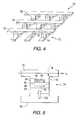
- FIG. 4is a schematic representation of a MRAM 70 constructed in accordance with this invention.
- MRAM 70includes a two-dimensional array of cells 72 , each including a MR element 74 .
- Word lines 76 , 78 and 80produce a magnetic field 82 along the hard axis of the MR elements, but the bit lines have been omitted.
- the bitis written via spin momentum transfer provided by a current perpendicular to the plane (CPP) flowing through the MR elements.
- CPPcurrent perpendicular to the plane
- FIG. 5is a cross-sectional view of a MR element 74 constructed in accordance with this invention.
- the MR elementincludes an antiferromagnetic layer 84 , a pinned layer 86 positioned adjacent to the antiferromagnetic layer, a free layer 88 , and a nonmagnetic layer 90 positioned between the pinned layer and the free layer.
- Arrow 92illustrates the direction of magnetization of the pinned layer.
- Arrows 94 and 96illustrate alternative directions of magnetization of the free layer.
- the MR element in this exampleis a CPP spin valve. The spin valve is connected between a word line 76 and a contact layer 98 .
- a current sourceis connected to the word line and the contact layer to supply electrical current to the spin valve during the writing process.
- the direction of magnetization of the free layercan be set into parallel and anti-parallel configurations with respect to the pinned layer by simply changing the direction of a CPP current of sufficient amplitude to cause switching.
- the currentcan be supplied through a suitable arrangement of diodes, transistors, or other components in accordance with known techniques.
- FIG. 6is a plot of the magnetization component along the easy axis M EA as a function of easy axis magnetic field H EA for a single-domain ferromagnetic particle having uniaxial anisotropy.
- the particleswitches its orientation by 180° when the easy axis field equals or exceeds the uniaxial anisotropy field, H K .
- H Kuniaxial anisotropy field
- FIG. 7is a plot of actual data from a CPP bottom spin valve having a rectangular cross-sectional area of approximately 10 4 nm 2 and the following layer structure from bottom-to-top: IrMn90/CoFe40/Ru10/CoFe40/Cu22/CoFe30, where the numbers refer to layer thicknesses in ⁇ .
- the anisotropy field of the free layeris approximately H K ⁇ 1500 Oe.
- the curves in FIG. 7are labeled to indicate the direction the current is being swept and the numbers represent the hard axis bias field.
- the CPP currentcan switch the orientation of the free layer with respect to the pinned layer via spin momentum transfer, as evidenced by abrupt changes in the resistance between the low resistance parallel and high resistance anti-parallel states.
- these current switching thresholdsdecrease with increasing hard axis bias field. Note that the switching thresholds are asymmetric about zero current due to small misalignment of the magnetic field with respect to the hard axis of the device.
- FIGS. 8, 9 and 10are cross-sectional views of alternative MR elements that can be used in combination with the hybrid write mechanism.
- FIG. 8shows a CPP spin valve structure 110 including a pinned layer 112 , a free layer 114 , and a nonmagnetic layer 116 positioned between the pinned layer and the free layer. An antiferromagnetic layer 118 is positioned adjacent to the pinned layer.
- First and second contacts, 120 and 122are provided on opposite sides of the CPP pillar and are connected to a current source 124 .
- Means generally indicated as block 126can further be provided to connect the current source to the pillar and to produce a signal in response to a change in resistance of the pillar during reading of the element.
- Arrow 128illustrates the direction of magnetization of the pinned layer.
- Arrows 130 and 132illustrate alternative directions of magnetization of the free layer.
- Arrows 134 and 136illustrate the direction of positive conventional electrical current.
- Arrow 138illustrates the direction of negative conventional electrical current.
- spin momentum transfer between the free layer and pinned layerwrites the bits, and magnetoresistance between these two layers is used to measure the relative configuration during read-back.
- FIG. 9shows a modification of the CPP spin valve whereby nano-oxide layers are inserted into the thin film multilayer in order to boost the resistance of the device and increase the amplitude of the read-back signal.
- FIG. 9shows a CPP spin valve structure 150 including a pinned layer 152 , a free layer 154 , and a nonmagnetic layer 156 positioned between the pinned layer and the free layer. An antiferromagnetic layer 158 is positioned adjacent to the pinned layer.
- First and second contacts, 160 and 162are provided on opposite sides of the CPP pillar and are connected to a current source 164 .
- Means generally indicated as block 166can further be provided to connect the current source to the pillar and to produce a signal in response to a change in resistance of the pillar during reading of the element.
- Arrows 168 and 170illustrate the direction of positive conventional electrical current.
- Arrow 172illustrates the direction of negative conventional electrical current.
- Nano-oxide layers 174 and 176are shown in layers 154 and 152 respectively. The magnetization directions of the free and pinned layers are aligned along the same directions as in FIG. 8.
- FIG. 10shows a magnetic tunnel junction that has a pinned reference layer and Cu spacer layer adjacent to the free layer.
- FIG. 10shows a CPP spin valve structure 180 including a pinned layer 182 , a free layer 184 , and a nonmagnetic insulating tunnel barrier layer 186 positioned between the pinned layer and the free layer.
- An antiferromagnetic layer 188is positioned adjacent to the pinned layer.
- An additional reference pinned layer 190is separated from the free layer 184 by a nonmagnetic layer 192 .
- First and second contacts, 194 and 196are provided on opposite sides of the CPP pillar and are connected to a current source 198 .
- Means generally indicated as block 200can further be provided to connect the current source to the pillar and to produce a signal in response to a change in resistance of the pillar during reading of the element.
- Arrow 202illustrates the direction of magnetization of the pinned layer 182 .
- Arrows 204 and 206illustrate alternative directions of magnetization of the free layer.
- Arrow 208illustrates the direction of magnetization of the reference pinned layer 190 .
- Arrows 210 and 212illustrate the direction of positive conventional electrical current.
- Arrow 214illustrates the direction of negative conventional electrical current.
- Spin momentum transfer between the free layer and pinned reference layer 190is used to write bits while the tunneling magnetoresistance between the free layer and pinned layer 182 is used to measure the free layer orientation during read-back.
- FIG. 11is a cross-sectional view of a portion of another MRAM 220 constructed in accordance with this invention.
- FIG. 12is a top view of a portion of a MRAM of FIG. 11.
- the magnetoresistive element 222includes a pinned layer 224 , a free layer 226 , and a nonmagnetic layer 228 positioned between the pinned layer and the free layer.
- An antiferromagnetic layer 230is positioned adjacent to the pinned layer.
- First and second leads, 232 and 234are provided on opposite sides of the CPP pillar and are connected to a current source.
- the leads 232 and 234 to the CPP pillarare configured so that the current flowing in the portion of lead 234 that is above lead 232 produces a magnetic field 236 along the hard axis of the free layer concurrently with a CPP current flowing through the pillar.
- the electrical leadsare insulated from each other and supported by insulating material, which has been omitted from FIGS. 11 and 12 for the sake of clarity.
- FIG. 12is a top view of the MR element 222 and electrical lead 234 .
- the electrical lead 234can be tapered in the region 238 near the element in order to locally boost the current density that will, in turn, produce larger hard axis bias fields.
- FIG. 13is a top view of a portion of another MRAM 250 constructed in accordance with this invention.
- FIG. 13shows a current carrying word line 252 that produces a field H W along the hard axis of a free layer within a MR element 254 . That field is used in combination with a CPP current to set the final free layer orientation with respect to the pinned layer via spin momentum transfer.
- the concept in FIG. 13can be extended by having two roughly orthogonal current carrying wires 262 and 264 that apply a magnetic field at a 45° angle with respect to the free layer hard axis of a CPP pillar 256 , as shown in FIG. 14.
- MRAM constructed in accordance with this inventioninclude a word line that produces a field along the hard axis of a MR element in a similar manner to the half-select process described above. However, the bit lines are replaced and now a CPP current is applied to the MR element. This CPP current will produce a spin transfer torque acting on the FL that, depending on current direction, will orient the FL either parallel or anti-parallel to the PL.
- FIGS. 6 and 7illustrate the well-known reduction in the switching field of a single domain magnetic particle when a hard axis field is applied.
- FIG. 6is simply another way of showing the data presented in FIG. 3.
- FIG. 7shows actual experimental data from a CPP bottom spin valve structure in which an external hard axis magnetic field lowers the current induced switching thresholds between the low resistance parallel and high resistance anti-parallel states. The application of a hard axis field will therefore make switching via spin transfer more efficient and enable the switching of FL's exhibiting significantly larger anisotropy compared to the case where spin transfer is the sole physical write mechanism.
- Equation 1⁇ right arrow over (m) ⁇ right arrow over (M) ⁇ /M S is the normalized magnetization
- ⁇is the gyromagnetic ratio
- ⁇ right arrow over (H) ⁇ effis the net magnetic field acting on the FL
- ⁇is the phenomenological damping coefficient
- Planck's constantj is the electrical current density
- gis a factor related to the spin polarization of conduction electrons
- eis the electron charge.
- the first two terms on the right hand side of Equation 1are the usual precession and damping terms.
- the third term on the rightis the torque due to spin transfer. A quick inspection of this last term reveals that the torque goes to zero when the FL and PL are either parallel or anti-parallel.
- spin transfer torqueis smallest when the MR element in the MRAM cell is in its quiescent state. Switching the FL 180° from this quiescent state by spin transfer alone consequently takes a relatively long time for two predominant reasons.
- thermal fluctuationsare necessary to produce small deflections of the FL magnetization away from being parallel or anti-parallel to the PL before the FL magnetization begins the switching process.
- spin transfer torqueis different in nature than the usual torque produced by a magnetic field such that it is necessary for the FL to undergo several precessional orbits around its initial direction before the magnetization rotates past 90° and into its new equilibrium direction.
- a dc hard axis fieldcan improve the efficiency and speed of switching via spin transfer. Further improvements can be made by exploiting the precessional overshoot of underdamped magnetic behavior, where the magnetization rotates around the equilibrium field direction largely set by the field from the word line. These improvements can be implemented by applying fast rise time current pulses through the word line that induces precession of the FL magnetization. The CPP current will then be synchronously applied at those instants when the FL magnetization overshoots its equilibrium configuration. The net result is that the FL can be switched using a smaller CPP current than that required when the magnetization has settled down into its static equilibrium direction.
- FIGS. 8, 9 and 10show three basic structures.
- FIG. 8shows a basic CPP spin valve having three essential features of a PL, FL, and a non-magnetic spacer layer.
- FIG. 9shows a CPP spin valve having a nano-oxide layer (NOL) in both the FL and PL, although a single NOL in either the FL or PL can also be used.
- NOLnano-oxide layer
- FIG. 10shows a magnetic tunnel junction with an additional pinned reference layer.
- the read-back signalis determined by the magnetoresistance of the FL and PL on either side of the insulating tunnel barrier.
- the write processis determined by the spin transfer torque acting within the FL, the pinned reference layer, and the non-magnetic metallic spacer layer in between.
- the PL for all three examplesis shown as a single layer of soft ferromagnetic material exchange biased by an antiferromagnet.
- other pinned layer structurescan equally be applied, such as a synthetic antiferromagnet (SAF) pinned via exchange coupling to an antiferromagnet or permanent magnet, a single permanent magnet layer, or a soft ferromagnet exchange coupled to a permanent magnet.
- SAFsynthetic antiferromagnet
- the pinned reference layer in FIG. 10is shown as a single layer for clarity.
- other structurescan be equally applied. These include a SAF pinned via exchange coupling to an antiferromagnet or permanent magnet, a single layer of permanent magnet, or a soft ferromagnet exchange coupled to a permanent magnet or an antiferromagnet.
- Typical antiferromagnetic materialsthat can be readily used include IrMn, PtMn, PtPdMn, and NiMn.
- Permanent magnet materialscan be CoPt, CoCrPt, FePt, or FePtCu.
- soft magnetic materialsinclude Co, CoFe, NiFe, and their alloys.
- the nonmagnetic metallic spacerscan be made from Cu, Ag, Au, or any other low resistance metal that efficiently transports spin polarized electrons from one ferromagnetic layer to another. Thicknesses of the layers are typically in the range of 1 to 15 nm.
- the anisotropy of the free layercan be tuned in the usual manner using shape anisotropy, where a rectangular shape will promote uniaxial anisotropy that favors having the magnetization aligned along the long axis of the rectangle.
- the shapecan be further refined by tapering the short sides of the rectangle into a point in order to promote single domain behavior in a now six-sided FL.
- the PLis unperturbed by the fields from the current carrying wires. Only the FL magnetization will be significantly influenced by any magnetic field supplied by the word line.
- the design shown in FIG. 4can be simplified using a lead geometry illustrated in FIG. 11.
- separate word linesare unnecessary as the electrical lead is wrapped around the MR element in such a way as to produce a hard axis field whenever a CPP current is applied to the device.
- the magnitude of the hard axis fieldis determined by the CPP current necessary to switch the FL via spin transfer and by the geometry of the lead.
- the hard axis fieldcan be tuned by varying the separation between the lead and the MR element, or by adjusting the cross-sectional area of the lead in the region where it overlaps the MR element.
- FIG. 13shows a top view of the basic elements necessary to implement the write process.
- the writing efficiencycan be further improved by using two orthogonal word lines to lower the energy barrier for magnetization reversal, and then orient the FL into its intended direction using spin transfer torque.
- This conceptis illustrated in FIG. 14.
- One word lineapplies a magnetic field along the hard axis while the second word line applies a field along the easy axis.
- the field from the second word lineis reversible, depending on current direction, and is directed along the same direction in which the FL magnetization is to be set.
- the second word lineincreases the switching efficiency of the FL via spin transfer, which is confirmed by the experimental data shown in FIG. 7.
- the fields from the two word linescan have arbitrary values as long as the fields are below the reversal threshold. But, the advantage of writing with two word lines in combination with spin transfer is maximized for the particular case of equal field magnitudes shown in FIG. 14. This is because this writing scheme takes the fullest advantage of reducing the barrier height by applying a magnetic field. The energy barrier for magnetization reversal is dependent upon the magnitude and direction of a magnetic field. Larger fields obviously reduce the barrier more than smaller fields.
- the energy barrier for magnetization reversalis maximum when the field is applied along the hard or easy axis and it is minimum (smaller by a factor of 2) when the field is applied 45° with respect to the anisotropy axis.
- the field applied to the selected cellis oriented along the 45° direction.
- the vector addition of the fields from the two word linesresults in a net field that is a factor of 1.4 times larger than that of each individual word line.
- this writing schememaximizes the writing efficiency of the selected cell and minimally impacts those cells along the two energized word lines.
- MRAMtypically also has some sort of series diode or transistor incorporated into each cell along with the MR element, the purpose of which is to properly direct the currents in the electrical circuitry during writing and read-back.
- This inventionprovides a method of writing bits in a MRAM device that uses a combination of conventional magnetic field and spin momentum transfer.
- the magnetic fieldis produced by a current carrying wire in much the same way as conventional MRAM.
- the final direction of the bitis set by the spin transfer torque from a CPP current.
- Previous patentshave proposed using only spin momentum transfer to write bits.
- this inventionovercomes the two issues of current efficiency and reversal speed by using a hybrid write mechanism. This invention improves the extensibility of MRAM to higher density and faster writing speeds.
Landscapes
- Engineering & Computer Science (AREA)
- Computer Hardware Design (AREA)
- Hall/Mr Elements (AREA)
- Mram Or Spin Memory Techniques (AREA)
Abstract
Description
- This invention relates to magnetic random access memory and, more particularly, to a method of writing to magnetic random access memory and magnetic random access memory that can be used to perform the method.[0001]
- Magnetic random access memory (MRAM) is a new technology that will likely provide superior performance over existing flash memory technology and may even supplant disk drives in certain low power applications requiring a compact non-volatile memory device. In MRAM, bits are represented by the magnetic configuration of a small volume of ferromagnetic material and its magnetic state is measured via a magnetoresistive (MR) effect during read-back. The MRAM typically includes a two-dimensional array of cells, with each cell containing one MR element that can store one bit.[0002]
- Most common MRAM designs employ MR elements that are based on either giant magnetoresistance (GMR) or tunneling magnetoresistance (TMR), where these elements are patterned thin film multilayer structures that include at least one pinned ferromagnetic layer (PL) and one free ferromagnetic layer (FL). These elements are designed so that the FL has a bistable magnetic configuration that is preferentially aligned along one out of a possible two anti-parallel directions. Hence, the binary data are stored as the orientation of the FL magnetization. The PL magnetization is aligned along only one of the two possible FL directions, and its role is to provide a fixed reference so that the magnetoresistance reveals the FL orientation with respect to the PL.[0003]
- There are numerous ways to implement a device based on this concept. However, the leading method to write bits is a so-called “half-select” process in which the magnetic fields generated by two roughly orthogonal current carrying wires orient the free layer into its intended configuration. All publicly disclosed MRAM prototypes to date have used this method. The amplitudes of the currents flowing through the two wires, referred to as the word and bit lines, are chosen so that the corresponding fields reverse a FL only where the two wires intersect. Therefore, this method can select any individual cell within the array with a minimum of electrical wires and without unintentionally reversing the magnetic state of other cells.[0004]
- Although MRAM has yet to reach the commercial market, it is likely that at least the first generation of products will employ a half-select write process. Unfortunately, this writing scheme exhibits poor scaling with increasing areal density of cells. MRAM faces the same issue of thermal stability that is confronting hard disk drives. In order to preserve the stability of the bits, the magnetic anisotropy of the FL will necessarily have to increase whenever the dimensions of the MR element decrease. This means that higher density MRAM will require larger magnetic fields in order to write bits, which will require larger currents through the word and bit lines that will consume more power. One way to improve the writing efficiency is to employ a thermally assisted writing scheme that reduces the FL anisotropy by heating the MR element. However, this write process will have to overcome numerous reliability issues related to the large increases in temperature required to make this scheme work. Thermally assisted writing will also face significant challenges in producing competitive writing speeds, as the process is fundamentally limited by the time (˜1 ns) it takes for thermal energy to transfer from the lattice (phonons) to the magnetic system.[0005]
- Another way to improve the writing efficiency of high density MRAM is to set the FL magnetization using the torque from an effect referred to as spin momentum transfer, as has been proposed in certain patents. Spin transfer is a phenomenon that occurs in current perpendicular to the plane (CPP) GMR devices that have cross-sectional areas on the order to 10[0006]4nm2or less. The strength of the torque is directly proportional to the current density through the CPP pillar. Therefore, for a given current, the current density will increase as the area of the CPP pillar decreases in size, and spin transfer will become more efficient as the density of MRAM increases. However, even a write process based on spin momentum transfer will have to confront the increasingly burdensome requirement of having to reverse the magnetization of a FL having a larger anisotropy. Furthermore, initial predictions indicate that a write process based on spin transfer alone can be slower at reversing the FL magnetization than writing with a conventional magnetic field.
- There is a need for a MRAM that can overcome the deficiencies of previous MRAM devices.[0007]
- A method of writing to a magnetic random access memory comprising: producing a magnetic field along a magnetically hard axis of a free layer of a magnetoresistive element; and passing current through the magnetoresistive element to change a direction of magnetization of the free layer by spin momentum transfer.[0008]
- The magnetic field along the magnetically hard axis of a free layer of a magnetoresistive element can be produced by passing a current through one or more conductors located adjacent to the magnetoresistive element.[0009]
- A single conductor can serve as the means for producing a magnetic field along a magnetically hard axis of a free layer of a magnetoresistive element and a connection for supplying current to the magnetoresistive element.[0010]
- The magnetic field along the magnetically hard axis of a free layer of a magnetoresistive element can cause the magnetization of the free layer to precess around an equilibrium direction, and the current through the magnetoresistive element can be applied at times when the magnetization of the free layer overshoots the equilibrium direction.[0011]
- In another aspect, the invention encompasses a magnetic random access memory comprising means for producing a magnetic field along a magnetically hard axis of a free layer of a magnetoresistive element, and means for passing current through the magnetoresistive element to change a direction of magnetization of the free layer by spin momentum transfer.[0012]
- The magnetoresistive element can comprise a pinned layer and a nonmagnetic layer positioned between the free layer and the pinned layer. A nano-oxide layer can be positioned in either the free layer, the pinned layer, or both the free layer and a pinned layer.[0013]
- The magnetoresistive element can alternatively comprise a first pinned layer; a first nonmagnetic layer positioned between the free layer and the pinned layer; a second pinned layer; and a second nonmagnetic layer positioned between the free layer and the pinned layer.[0014]
- FIG. 1 is a schematic representation of a prior art MRAM.[0015]
- FIG. 2 is a cross-sectional view of a prior art MR element.[0016]
- FIG. 3 is a graph of energy versus magnetization angle for a MR element.[0017]
- FIG. 4 is a schematic representation of a MRAM constructed in accordance with this invention.[0018]
- FIG. 5 is a cross-sectional view of a MR element constructed in accordance with this invention.[0019]
- FIG. 6 is a graph of magnetization versus magnetic field for a free layer within a MR element.[0020]
- FIG. 7 is a graph of resistance versus current of a MR element.[0021]
- FIGS. 8, 9 and[0022]10 are cross-sectional views of alternative MR elements constructed in accordance with this invention.
- FIG. 11 is a cross-sectional view of a portion of a MRAM constructed in accordance with this invention.[0023]
- FIG. 12 is a top view of a portion of the MRAM of FIG. 11.[0024]
- FIG. 13 is a top view of a portion of another MRAM constructed in accordance with this invention.[0025]
- FIG. 14 is a top view of a portion of another MRAM constructed in accordance with this invention.[0026]
- Referring to the drawings, FIG. 1 is a schematic representation of a conventional magnetic[0027]
random access memory 10. MRAM10 includes a 3×3 array ofcells 12 that are a subset of the total number of cells comprising the MRAM device. Every cell contains oneMR element 14. There are two roughly orthogonal sets of electrical wires, referred to asword lines bit lines - FIG. 2 is a cross-sectional view of a[0028]
MR element 14, which for this particular example is a magnetic tunnel junction. The MR element is connected between aword line 16 and abit line 22, and includes anantiferromagnetic layer 28, a pinned layer30 positioned on the antiferromagnetic layer, afree layer 32, and anonmagnetic layer 34 between the pinned layer and the free layer. Thearrows arrow 40 in the pinned layer indicate the direction of magnetization. Current passing through the word line produces afield 42 along the hard axis of the free layer. Current passing through the bit line produces afield 44 along the easy axis of the free layer. - The half-select process is further illustrated in FIG. 3.[0029]
Curve 46 shows the energy versus magnetization angle for a FL in its quiescent state with assumed uniaxial anisotropy. There are two preferredmagnetic orientations curve 46, that correspond to the points of minimum energy. A current passing through the word line produces a field along the hard axis of the FL with an amplitude that is roughly one half of the anisotropy field, HK. Curve52 shows that this field lowers the energy barrier for magnetization reversal, but the magnetization is still “trapped” in an energy minimum close to its initial state as illustrated bydot 54. A current passing through the bit line produces a field along the easy axis of the FL in a direction that sets the final orientation of the FL magnetization. This field also lowers the energy barrier for magnetization reversal but, as is the case for the hard axis field from the word line, the magnetization stays in themetastable energy minimum 56 around its initial configuration, as shown incurve 58. Only the simultaneous application of these two fields will drive the FL magnetization to anew configuration 180° away from its initial state.Curve 60 illustrates how these fields eliminate the energy barrier, leaving only one energetically preferredstate 62 in a direction determined by the direction of the field from the bit line. - FIG. 3 illustrates the “half-select” write mechanism for reversing the magnetization of a single-domain ferromagnetic particle having uniaxial anisotropy. The dashed[0030]
line 64 indicates a hypothetical initial magnetization direction, and the dots indicate the equilibrium state of the magnetization for all four situations.Curve 46 represents energy as a function of the angle of the magnetization in the absence of an external magnetic field.Curve 52 represents energy when the word line produces a magnetic field equal to 0.4*HKalong the hard axis, or 90° direction.Curve 58 represents energy when the bit line produces a field of 0.4*HKalong the easy axis, or 0° direction.Curve 60 represents energy when both hard and easy axis fields are applied by the word and bit lines, respectively. This occurs only at the cell where the word and bit lines overlap, and it is the combination of these two fields that drives the magnetization into its new orientation. - This invention provides a different write process that uses a combination of spin momentum transfer and the conventional magnetic field from a current carrying wire. FIG. 4 is a schematic representation of a[0031]
MRAM 70 constructed in accordance with this invention.MRAM 70 includes a two-dimensional array ofcells 72, each including aMR element 74. Word lines76,78 and80 produce amagnetic field 82 along the hard axis of the MR elements, but the bit lines have been omitted. The bit is written via spin momentum transfer provided by a current perpendicular to the plane (CPP) flowing through the MR elements. - FIG. 5 is a cross-sectional view of a[0032]
MR element 74 constructed in accordance with this invention. The MR element includes anantiferromagnetic layer 84, a pinnedlayer 86 positioned adjacent to the antiferromagnetic layer, afree layer 88, and anonmagnetic layer 90 positioned between the pinned layer and the free layer.Arrow 92 illustrates the direction of magnetization of the pinned layer.Arrows word line 76 and acontact layer 98. A current source, not shown, is connected to the word line and the contact layer to supply electrical current to the spin valve during the writing process. There is a torque acting on the free layer due to spin transfer whenever a CPP current is driven through the stack as illustrated byarrow 100. The direction of magnetization of the free layer can be set into parallel and anti-parallel configurations with respect to the pinned layer by simply changing the direction of a CPP current of sufficient amplitude to cause switching. The current can be supplied through a suitable arrangement of diodes, transistors, or other components in accordance with known techniques. - FIG. 6 is a plot of the magnetization component along the easy axis M[0033]EAas a function of easy axis magnetic field HEAfor a single-domain ferromagnetic particle having uniaxial anisotropy. With no hard axis field applied, as illustrated by
curve 102, the particle switches its orientation by 180° when the easy axis field equals or exceeds the uniaxial anisotropy field, HK. When a hard axis field of 0.4*HKis applied, as illustrated bycurve 104, the particle will switch at fields that are much less than HK. FIG. 7 is a plot of actual data from a CPP bottom spin valve having a rectangular cross-sectional area of approximately 104nm2and the following layer structure from bottom-to-top: IrMn90/CoFe40/Ru10/CoFe40/Cu22/CoFe30, where the numbers refer to layer thicknesses in Å. The anisotropy field of the free layer is approximately HK˜1500 Oe. The curves in FIG. 7 are labeled to indicate the direction the current is being swept and the numbers represent the hard axis bias field. - The CPP current can switch the orientation of the free layer with respect to the pinned layer via spin momentum transfer, as evidenced by abrupt changes in the resistance between the low resistance parallel and high resistance anti-parallel states. In an analogous manner as the field-induced switching shown in FIG. 6, these current switching thresholds decrease with increasing hard axis bias field. Note that the switching thresholds are asymmetric about zero current due to small misalignment of the magnetic field with respect to the hard axis of the device.[0034]
- FIGS. 8, 9 and[0035]10 are cross-sectional views of alternative MR elements that can be used in combination with the hybrid write mechanism. FIG. 8 shows a CPP spin valve structure110 including a pinned
layer 112, afree layer 114, and anonmagnetic layer 116 positioned between the pinned layer and the free layer. Anantiferromagnetic layer 118 is positioned adjacent to the pinned layer. First and second contacts,120 and122, are provided on opposite sides of the CPP pillar and are connected to acurrent source 124. Means generally indicated asblock 126 can further be provided to connect the current source to the pillar and to produce a signal in response to a change in resistance of the pillar during reading of the element.Arrow 128 illustrates the direction of magnetization of the pinned layer.Arrows Arrows Arrow 138 illustrates the direction of negative conventional electrical current. In the structure of FIG. 8, spin momentum transfer between the free layer and pinned layer writes the bits, and magnetoresistance between these two layers is used to measure the relative configuration during read-back. - FIG. 9 shows a modification of the CPP spin valve whereby nano-oxide layers are inserted into the thin film multilayer in order to boost the resistance of the device and increase the amplitude of the read-back signal. FIG. 9 shows a CPP spin valve structure[0036]150 including a pinned
layer 152, afree layer 154, and anonmagnetic layer 156 positioned between the pinned layer and the free layer. Anantiferromagnetic layer 158 is positioned adjacent to the pinned layer. First and second contacts,160 and162, are provided on opposite sides of the CPP pillar and are connected to acurrent source 164. Means generally indicated asblock 166 can further be provided to connect the current source to the pillar and to produce a signal in response to a change in resistance of the pillar during reading of the element.Arrows Arrow 172 illustrates the direction of negative conventional electrical current. Nano-oxide layers layers - FIG. 10 shows a magnetic tunnel junction that has a pinned reference layer and Cu spacer layer adjacent to the free layer. FIG. 10 shows a CPP[0037]
spin valve structure 180 including a pinnedlayer 182, afree layer 184, and a nonmagnetic insulatingtunnel barrier layer 186 positioned between the pinned layer and the free layer. Anantiferromagnetic layer 188 is positioned adjacent to the pinned layer. An additional reference pinnedlayer 190 is separated from thefree layer 184 by anonmagnetic layer 192. First and second contacts,194 and196, are provided on opposite sides of the CPP pillar and are connected to acurrent source 198. Means generally indicated asblock 200 can further be provided to connect the current source to the pillar and to produce a signal in response to a change in resistance of the pillar during reading of the element.Arrow 202 illustrates the direction of magnetization of the pinnedlayer 182. Arrows204 and206 illustrate alternative directions of magnetization of the free layer. Arrow208 illustrates the direction of magnetization of the reference pinnedlayer 190.Arrows Arrow 214 illustrates the direction of negative conventional electrical current. Spin momentum transfer between the free layer and pinnedreference layer 190 is used to write bits while the tunneling magnetoresistance between the free layer and pinnedlayer 182 is used to measure the free layer orientation during read-back. - FIG. 11 is a cross-sectional view of a portion of another MRAM[0038]220 constructed in accordance with this invention. FIG. 12 is a top view of a portion of a MRAM of FIG. 11. The
magnetoresistive element 222 includes a pinnedlayer 224, afree layer 226, and anonmagnetic layer 228 positioned between the pinned layer and the free layer. Anantiferromagnetic layer 230 is positioned adjacent to the pinned layer. First and second leads,232 and234, are provided on opposite sides of the CPP pillar and are connected to a current source. The leads232 and234 to the CPP pillar are configured so that the current flowing in the portion oflead 234 that is abovelead 232 produces amagnetic field 236 along the hard axis of the free layer concurrently with a CPP current flowing through the pillar. The electrical leads are insulated from each other and supported by insulating material, which has been omitted from FIGS. 11 and 12 for the sake of clarity. FIG. 12 is a top view of theMR element 222 andelectrical lead 234. Theelectrical lead 234 can be tapered in theregion 238 near the element in order to locally boost the current density that will, in turn, produce larger hard axis bias fields. - FIG. 13 is a top view of a portion of another[0039]
MRAM 250 constructed in accordance with this invention. FIG. 13 shows a current carryingword line 252 that produces a field HWalong the hard axis of a free layer within aMR element 254. That field is used in combination with a CPP current to set the final free layer orientation with respect to the pinned layer via spin momentum transfer. The concept in FIG. 13 can be extended by having two roughly orthogonal current carryingwires - MRAM constructed in accordance with this invention include a word line that produces a field along the hard axis of a MR element in a similar manner to the half-select process described above. However, the bit lines are replaced and now a CPP current is applied to the MR element. This CPP current will produce a spin transfer torque acting on the FL that, depending on current direction, will orient the FL either parallel or anti-parallel to the PL.[0040]
- One of the advantages of going to a hybrid write mechanism is illustrated in FIGS. 6 and 7. FIG. 6 illustrates the well-known reduction in the switching field of a single domain magnetic particle when a hard axis field is applied. FIG. 6 is simply another way of showing the data presented in FIG. 3. However, the same principle can also be applied to switching via spin momentum transfer. FIG. 7 shows actual experimental data from a CPP bottom spin valve structure in which an external hard axis magnetic field lowers the current induced switching thresholds between the low resistance parallel and high resistance anti-parallel states. The application of a hard axis field will therefore make switching via spin transfer more efficient and enable the switching of FL's exhibiting significantly larger anisotropy compared to the case where spin transfer is the sole physical write mechanism.[0041]
- In addition to these gains in efficiency, the hard axis field will also lead to faster switching speeds than if spin transfer were to be used by itself. This is illustrated by the Landau-Lifshitz equation of motion:[0042]
- ∂{right arrow over (m)}FL/∂t=−γ{right arrow over (m)}FL×[{right arrow over (H)}eff+α{right arrow over (m)}FL×{right arrow over (H)}eff]+(jg/e){right arrow over (m)}FL×{right arrow over (m)}FL×{right arrow over (m)}PL, (1)

- where {right arrow over (m)}≡{right arrow over (M)}/M[0043]Sis the normalized magnetization, γ is the gyromagnetic ratio, {right arrow over (H)}effis the net magnetic field acting on the FL, α is the phenomenological damping coefficient,is Planck's constant, j is the electrical current density, g is a factor related to the spin polarization of conduction electrons, and e is the electron charge. The first two terms on the right hand side of
Equation 1 are the usual precession and damping terms. The third term on the right is the torque due to spin transfer. A quick inspection of this last term reveals that the torque goes to zero when the FL and PL are either parallel or anti-parallel. In other words, spin transfer torque is smallest when the MR element in the MRAM cell is in its quiescent state. Switching theFL 180° from this quiescent state by spin transfer alone consequently takes a relatively long time for two predominant reasons. First, thermal fluctuations are necessary to produce small deflections of the FL magnetization away from being parallel or anti-parallel to the PL before the FL magnetization begins the switching process. Second, spin transfer torque is different in nature than the usual torque produced by a magnetic field such that it is necessary for the FL to undergo several precessional orbits around its initial direction before the magnetization rotates past 90° and into its new equilibrium direction. In contrast, the application of a hard axis field will deflect the FL into a state where there is a non-zero angle between the FL and PL magnetizations. Thus, the spin transfer torque produced by a CPP current will initially be large, thereby circumventing the long build up in angle required when spin transfer acts alone. - Therefore, a dc hard axis field can improve the efficiency and speed of switching via spin transfer. Further improvements can be made by exploiting the precessional overshoot of underdamped magnetic behavior, where the magnetization rotates around the equilibrium field direction largely set by the field from the word line. These improvements can be implemented by applying fast rise time current pulses through the word line that induces precession of the FL magnetization. The CPP current will then be synchronously applied at those instants when the FL magnetization overshoots its equilibrium configuration. The net result is that the FL can be switched using a smaller CPP current than that required when the magnetization has settled down into its static equilibrium direction.[0044]
- Many different types of MR elements are compatible with the proposed write mechanism. The only major constraint is that electrical leads should be connected in such a way as to pass a CPP current through the pillar. Examples of three basic structures are shown in FIGS. 8, 9 and[0045]10. FIG. 8 shows a basic CPP spin valve having three essential features of a PL, FL, and a non-magnetic spacer layer. FIG. 9 shows a CPP spin valve having a nano-oxide layer (NOL) in both the FL and PL, although a single NOL in either the FL or PL can also be used. The advantage of incorporating a NOL is that this increases the magnetoresistance, which will improve the power efficiency and amplitude of the read-back signal.
- FIG. 10 shows a magnetic tunnel junction with an additional pinned reference layer. The read-back signal is determined by the magnetoresistance of the FL and PL on either side of the insulating tunnel barrier. The write process is determined by the spin transfer torque acting within the FL, the pinned reference layer, and the non-magnetic metallic spacer layer in between.[0046]
- Note that the PL for all three examples is shown as a single layer of soft ferromagnetic material exchange biased by an antiferromagnet. However, other pinned layer structures can equally be applied, such as a synthetic antiferromagnet (SAF) pinned via exchange coupling to an antiferromagnet or permanent magnet, a single permanent magnet layer, or a soft ferromagnet exchange coupled to a permanent magnet. The pinned reference layer in FIG. 10 is shown as a single layer for clarity. As is the case for the PL, other structures can be equally applied. These include a SAF pinned via exchange coupling to an antiferromagnet or permanent magnet, a single layer of permanent magnet, or a soft ferromagnet exchange coupled to a permanent magnet or an antiferromagnet.[0047]
- There is a wide latitude for the choice of materials and their thicknesses within the CPP stacks. Typical antiferromagnetic materials that can be readily used include IrMn, PtMn, PtPdMn, and NiMn. Permanent magnet materials can be CoPt, CoCrPt, FePt, or FePtCu. Examples of soft magnetic materials include Co, CoFe, NiFe, and their alloys. The nonmagnetic metallic spacers can be made from Cu, Ag, Au, or any other low resistance metal that efficiently transports spin polarized electrons from one ferromagnetic layer to another. Thicknesses of the layers are typically in the range of 1 to 15 nm.[0048]
- The anisotropy of the free layer can be tuned in the usual manner using shape anisotropy, where a rectangular shape will promote uniaxial anisotropy that favors having the magnetization aligned along the long axis of the rectangle. The shape can be further refined by tapering the short sides of the rectangle into a point in order to promote single domain behavior in a now six-sided FL. Lastly, it is implicit in this disclosure that the PL is unperturbed by the fields from the current carrying wires. Only the FL magnetization will be significantly influenced by any magnetic field supplied by the word line.[0049]
- The design shown in FIG. 4 can be simplified using a lead geometry illustrated in FIG. 11. In this simplified design, separate word lines are unnecessary as the electrical lead is wrapped around the MR element in such a way as to produce a hard axis field whenever a CPP current is applied to the device. The magnitude of the hard axis field is determined by the CPP current necessary to switch the FL via spin transfer and by the geometry of the lead. The hard axis field can be tuned by varying the separation between the lead and the MR element, or by adjusting the cross-sectional area of the lead in the region where it overlaps the MR element.[0050]
- Another extension of the proposed design is presented in FIG. 13. FIG. 13 shows a top view of the basic elements necessary to implement the write process. However, the writing efficiency can be further improved by using two orthogonal word lines to lower the energy barrier for magnetization reversal, and then orient the FL into its intended direction using spin transfer torque. This concept is illustrated in FIG. 14. One word line applies a magnetic field along the hard axis while the second word line applies a field along the easy axis. The field from the second word line is reversible, depending on current direction, and is directed along the same direction in which the FL magnetization is to be set. In other words, the second word line increases the switching efficiency of the FL via spin transfer, which is confirmed by the experimental data shown in FIG. 7.[0051]
- In general, the fields from the two word lines can have arbitrary values as long as the fields are below the reversal threshold. But, the advantage of writing with two word lines in combination with spin transfer is maximized for the particular case of equal field magnitudes shown in FIG. 14. This is because this writing scheme takes the fullest advantage of reducing the barrier height by applying a magnetic field. The energy barrier for magnetization reversal is dependent upon the magnitude and direction of a magnetic field. Larger fields obviously reduce the barrier more than smaller fields. But, for a given field amplitude, the energy barrier for magnetization reversal is maximum when the field is applied along the hard or easy axis and it is minimum (smaller by a factor of 2) when the field is applied 45° with respect to the anisotropy axis. For the example in FIG. 14, the field applied to the selected cell is oriented along the 45° direction. Moreover, the vector addition of the fields from the two word lines results in a net field that is a factor of 1.4 times larger than that of each individual word line. Hence, this writing scheme maximizes the writing efficiency of the selected cell and minimally impacts those cells along the two energized word lines.[0052]
- The above examples have focused solely on the method of writing and on possible MR elements that can be used for such a method. In another aspect of the invention, the MR elements can be incorporated into various MRAM architectures beyond the specific example presented in FIG. 4.[0053]
- Another important point is that MRAM typically also has some sort of series diode or transistor incorporated into each cell along with the MR element, the purpose of which is to properly direct the currents in the electrical circuitry during writing and read-back. These additional components have been omitted from the FIGs. for the sake of clarity, and it is an implicit assumption that the MRAM of this disclosure can incorporate whatever additional components are necessary to perform the write mechanism and to incorporate the MR elements into a system level architecture.[0054]
- This invention provides a method of writing bits in a MRAM device that uses a combination of conventional magnetic field and spin momentum transfer. The magnetic field is produced by a current carrying wire in much the same way as conventional MRAM. However, the final direction of the bit is set by the spin transfer torque from a CPP current. Previous patents have proposed using only spin momentum transfer to write bits. In contrast, this invention overcomes the two issues of current efficiency and reversal speed by using a hybrid write mechanism. This invention improves the extensibility of MRAM to higher density and faster writing speeds.[0055]
- While the invention has been described in term of several examples, it will be apparent to those skilled in the art that various changes can be made to the disclosed examples without departing from the scope of the invention as defined by the following claims.[0056]

Claims (19)
Priority Applications (1)
| Application Number | Priority Date | Filing Date | Title |
|---|---|---|---|
| US10/456,451US7006375B2 (en) | 2003-06-06 | 2003-06-06 | Hybrid write mechanism for high speed and high density magnetic random access memory |
Applications Claiming Priority (1)
| Application Number | Priority Date | Filing Date | Title |
|---|---|---|---|
| US10/456,451US7006375B2 (en) | 2003-06-06 | 2003-06-06 | Hybrid write mechanism for high speed and high density magnetic random access memory |
Publications (2)
| Publication Number | Publication Date |
|---|---|
| US20040246775A1true US20040246775A1 (en) | 2004-12-09 |
| US7006375B2 US7006375B2 (en) | 2006-02-28 |
Family
ID=33490176
Family Applications (1)
| Application Number | Title | Priority Date | Filing Date |
|---|---|---|---|
| US10/456,451Expired - Fee RelatedUS7006375B2 (en) | 2003-06-06 | 2003-06-06 | Hybrid write mechanism for high speed and high density magnetic random access memory |
Country Status (1)
| Country | Link |
|---|---|
| US (1) | US7006375B2 (en) |
Cited By (11)
| Publication number | Priority date | Publication date | Assignee | Title |
|---|---|---|---|---|
| US20070253121A1 (en)* | 2006-04-26 | 2007-11-01 | Masaki Yamada | Spin accumulation device and magnetic sensor applied with spin current confined layer |
| US20080037179A1 (en)* | 2006-05-04 | 2008-02-14 | Kenchi Ito | Magnetic memory device |
| US20080247223A1 (en)* | 2005-10-28 | 2008-10-09 | Tomoaki Inokuchi | Spin-injection magnetic random access memory |
| US7502249B1 (en)* | 2006-07-17 | 2009-03-10 | Grandis, Inc. | Method and system for using a pulsed field to assist spin transfer induced switching of magnetic memory elements |
| US20100067281A1 (en)* | 2008-09-15 | 2010-03-18 | Seagate Technology Llc | Variable write and read methods for resistive random access memory |
| US8411497B2 (en) | 2010-05-05 | 2013-04-02 | Grandis, Inc. | Method and system for providing a magnetic field aligned spin transfer torque random access memory |
| US20140010004A1 (en)* | 2011-03-22 | 2014-01-09 | Renesas Electronics Corporation | Magnetic memory |
| US10424726B2 (en) | 2017-12-28 | 2019-09-24 | Spin Memory, Inc. | Process for improving photoresist pillar adhesion during MRAM fabrication |
| US10446210B2 (en) | 2016-09-27 | 2019-10-15 | Spin Memory, Inc. | Memory instruction pipeline with a pre-read stage for a write operation for reducing power consumption in a memory device that uses dynamic redundancy registers |
| US10460781B2 (en) | 2016-09-27 | 2019-10-29 | Spin Memory, Inc. | Memory device with a dual Y-multiplexer structure for performing two simultaneous operations on the same row of a memory bank |
| US11132135B2 (en)* | 2019-04-11 | 2021-09-28 | International Business Machines Corporation | Dynamic disk replication mode selection based on storage area network latency |
Families Citing this family (114)
| Publication number | Priority date | Publication date | Assignee | Title |
|---|---|---|---|---|
| FR2866750B1 (en)* | 2004-02-23 | 2006-04-21 | Centre Nat Rech Scient | MAGNETIC MEMORY MEMORY WITH MAGNETIC TUNNEL JUNCTION AND METHOD FOR ITS WRITING |
| US7576956B2 (en)* | 2004-07-26 | 2009-08-18 | Grandis Inc. | Magnetic tunnel junction having diffusion stop layer |
| DE102004042338B4 (en)* | 2004-09-01 | 2006-09-07 | Infineon Technologies Ag | MRAM with improved memory and readout characteristics |
| KR100754930B1 (en)* | 2004-12-22 | 2007-09-03 | 한국과학기술원 | MRM element of voltage controlled magnetization inversion recording method and method of recording and reading information using the same |
| US7224601B2 (en)* | 2005-08-25 | 2007-05-29 | Grandis Inc. | Oscillating-field assisted spin torque switching of a magnetic tunnel junction memory element |
| US7973349B2 (en)* | 2005-09-20 | 2011-07-05 | Grandis Inc. | Magnetic device having multilayered free ferromagnetic layer |
| US7859034B2 (en)* | 2005-09-20 | 2010-12-28 | Grandis Inc. | Magnetic devices having oxide antiferromagnetic layer next to free ferromagnetic layer |
| US7777261B2 (en) | 2005-09-20 | 2010-08-17 | Grandis Inc. | Magnetic device having stabilized free ferromagnetic layer |
| US7430135B2 (en)* | 2005-12-23 | 2008-09-30 | Grandis Inc. | Current-switched spin-transfer magnetic devices with reduced spin-transfer switching current density |
| US20070246787A1 (en)* | 2006-03-29 | 2007-10-25 | Lien-Chang Wang | On-plug magnetic tunnel junction devices based on spin torque transfer switching |
| US7532505B1 (en) | 2006-07-17 | 2009-05-12 | Grandis, Inc. | Method and system for using a pulsed field to assist spin transfer induced switching of magnetic memory elements |
| US7851840B2 (en)* | 2006-09-13 | 2010-12-14 | Grandis Inc. | Devices and circuits based on magnetic tunnel junctions utilizing a multilayer barrier |
| US7589600B2 (en)* | 2006-10-31 | 2009-09-15 | Seagate Technology Llc | Spin oscillator device |
| US7508042B2 (en) | 2006-12-22 | 2009-03-24 | Magic Technologies, Inc. | Spin transfer MRAM device with magnetic biasing |
| US7742329B2 (en)* | 2007-03-06 | 2010-06-22 | Qualcomm Incorporated | Word line transistor strength control for read and write in spin transfer torque magnetoresistive random access memory |
| US7859069B2 (en)* | 2007-03-16 | 2010-12-28 | Seagate Technology Llc | Magnetic storage element with storage layer magnetization directed for increased responsiveness to spin polarized current |
| US7852662B2 (en)* | 2007-04-24 | 2010-12-14 | Magic Technologies, Inc. | Spin-torque MRAM: spin-RAM, array |
| US7957179B2 (en)* | 2007-06-27 | 2011-06-07 | Grandis Inc. | Magnetic shielding in magnetic multilayer structures |
| US7750421B2 (en)* | 2007-07-23 | 2010-07-06 | Magic Technologies, Inc. | High performance MTJ element for STT-RAM and method for making the same |
| US7982275B2 (en)* | 2007-08-22 | 2011-07-19 | Grandis Inc. | Magnetic element having low saturation magnetization |
| US20090103354A1 (en)* | 2007-10-17 | 2009-04-23 | Qualcomm Incorporated | Ground Level Precharge Bit Line Scheme for Read Operation in Spin Transfer Torque Magnetoresistive Random Access Memory |
| US7898849B2 (en)* | 2007-12-05 | 2011-03-01 | Seagate Technology, Llc | Compound cell spin-torque magnetic random access memory |
| US7999336B2 (en)* | 2008-04-24 | 2011-08-16 | Seagate Technology Llc | ST-RAM magnetic element configurations to reduce switching current |
| US7894248B2 (en)* | 2008-09-12 | 2011-02-22 | Grandis Inc. | Programmable and redundant circuitry based on magnetic tunnel junction (MTJ) |
| US8320175B2 (en)* | 2009-02-27 | 2012-11-27 | Magsil Corporation | Magnetic booster for magnetic random access memory |
| US9171601B2 (en) | 2009-07-08 | 2015-10-27 | Alexander Mikhailovich Shukh | Scalable magnetic memory cell with reduced write current |
| US8406041B2 (en) | 2009-07-08 | 2013-03-26 | Alexander Mikhailovich Shukh | Scalable magnetic memory cell with reduced write current |
| US8411494B2 (en) | 2009-07-21 | 2013-04-02 | Alexander Mikhailovich Shukh | Three-dimensional magnetic random access memory with high speed writing |
| US8331141B2 (en) | 2009-08-05 | 2012-12-11 | Alexander Mikhailovich Shukh | Multibit cell of magnetic random access memory with perpendicular magnetization |
| EP2325846B1 (en)* | 2009-11-12 | 2015-10-28 | Crocus Technology S.A. | A magnetic tunnel junction memory with thermally assisted writing |
| US8625340B1 (en) | 2010-02-26 | 2014-01-07 | Magsil Corporation | Magnetic sidewalls for write lines in field-induced MRAM and methods of manufacturing them |
| US8988934B2 (en) | 2010-07-27 | 2015-03-24 | Alexander Mikhailovich Shukh | Multibit cell of magnetic random access memory with perpendicular magnetization |
| US9666639B2 (en) | 2010-09-17 | 2017-05-30 | Micron Technology, Inc. | Spin torque transfer memory cell structures and methods |
| US8300454B2 (en) | 2010-09-17 | 2012-10-30 | Micron Technology, Inc. | Spin torque transfer memory cell structures and methods |
| US8358534B2 (en) | 2010-09-17 | 2013-01-22 | Micron Technology, Inc. | Spin torque transfer memory cell structures and methods |
| US8310868B2 (en) | 2010-09-17 | 2012-11-13 | Micron Technology, Inc. | Spin torque transfer memory cell structures and methods |
| US9070456B2 (en) | 2011-04-07 | 2015-06-30 | Tom A. Agan | High density magnetic random access memory |
| US8976577B2 (en) | 2011-04-07 | 2015-03-10 | Tom A. Agan | High density magnetic random access memory |
| EP2608208B1 (en)* | 2011-12-22 | 2015-02-11 | Crocus Technology S.A. | Self-referenced MRAM cell and method for writing the cell using a spin transfer torque write operation |
| US9214212B2 (en)* | 2012-12-03 | 2015-12-15 | Taiwan Semiconductor Manufacturing Company, Ltd. | Magnetic tunnel junction memory device |
| US9251816B2 (en) | 2013-10-03 | 2016-02-02 | Seagate Technology Llc | Magnetic sensor shield pinned by a high-coercivity ferromagnet |
| US9263667B1 (en) | 2014-07-25 | 2016-02-16 | Spin Transfer Technologies, Inc. | Method for manufacturing MTJ memory device |
| US9337412B2 (en) | 2014-09-22 | 2016-05-10 | Spin Transfer Technologies, Inc. | Magnetic tunnel junction structure for MRAM device |
| JP6451362B2 (en)* | 2015-02-04 | 2019-01-16 | Tdk株式会社 | Magnetoresistive device |
| US10468590B2 (en) | 2015-04-21 | 2019-11-05 | Spin Memory, Inc. | High annealing temperature perpendicular magnetic anisotropy structure for magnetic random access memory |
| US9728712B2 (en) | 2015-04-21 | 2017-08-08 | Spin Transfer Technologies, Inc. | Spin transfer torque structure for MRAM devices having a spin current injection capping layer |
| US9853206B2 (en) | 2015-06-16 | 2017-12-26 | Spin Transfer Technologies, Inc. | Precessional spin current structure for MRAM |
| US9773974B2 (en) | 2015-07-30 | 2017-09-26 | Spin Transfer Technologies, Inc. | Polishing stop layer(s) for processing arrays of semiconductor elements |
| US10163479B2 (en) | 2015-08-14 | 2018-12-25 | Spin Transfer Technologies, Inc. | Method and apparatus for bipolar memory write-verify |
| US9490297B1 (en) | 2015-09-30 | 2016-11-08 | HGST Netherlands B.V. | Half select method and structure for gating rashba or spin hall MRAM |
| US9741926B1 (en) | 2016-01-28 | 2017-08-22 | Spin Transfer Technologies, Inc. | Memory cell having magnetic tunnel junction and thermal stability enhancement layer |
| US10360964B2 (en) | 2016-09-27 | 2019-07-23 | Spin Memory, Inc. | Method of writing contents in memory during a power up sequence using a dynamic redundancy register in a memory device |
| US11119910B2 (en) | 2016-09-27 | 2021-09-14 | Spin Memory, Inc. | Heuristics for selecting subsegments for entry in and entry out operations in an error cache system with coarse and fine grain segments |
| US10366774B2 (en) | 2016-09-27 | 2019-07-30 | Spin Memory, Inc. | Device with dynamic redundancy registers |
| US10818331B2 (en) | 2016-09-27 | 2020-10-27 | Spin Memory, Inc. | Multi-chip module for MRAM devices with levels of dynamic redundancy registers |
| US10628316B2 (en) | 2016-09-27 | 2020-04-21 | Spin Memory, Inc. | Memory device with a plurality of memory banks where each memory bank is associated with a corresponding memory instruction pipeline and a dynamic redundancy register |
| US10437491B2 (en) | 2016-09-27 | 2019-10-08 | Spin Memory, Inc. | Method of processing incomplete memory operations in a memory device during a power up sequence and a power down sequence using a dynamic redundancy register |
| US11119936B2 (en) | 2016-09-27 | 2021-09-14 | Spin Memory, Inc. | Error cache system with coarse and fine segments for power optimization |
| US11151042B2 (en) | 2016-09-27 | 2021-10-19 | Integrated Silicon Solution, (Cayman) Inc. | Error cache segmentation for power reduction |
| US10546625B2 (en) | 2016-09-27 | 2020-01-28 | Spin Memory, Inc. | Method of optimizing write voltage based on error buffer occupancy |
| US10991410B2 (en) | 2016-09-27 | 2021-04-27 | Spin Memory, Inc. | Bi-polar write scheme |
| US10437723B2 (en) | 2016-09-27 | 2019-10-08 | Spin Memory, Inc. | Method of flushing the contents of a dynamic redundancy register to a secure storage area during a power down in a memory device |
| US10665777B2 (en) | 2017-02-28 | 2020-05-26 | Spin Memory, Inc. | Precessional spin current structure with non-magnetic insertion layer for MRAM |
| US10672976B2 (en) | 2017-02-28 | 2020-06-02 | Spin Memory, Inc. | Precessional spin current structure with high in-plane magnetization for MRAM |
| US10032978B1 (en) | 2017-06-27 | 2018-07-24 | Spin Transfer Technologies, Inc. | MRAM with reduced stray magnetic fields |
| US10481976B2 (en) | 2017-10-24 | 2019-11-19 | Spin Memory, Inc. | Forcing bits as bad to widen the window between the distributions of acceptable high and low resistive bits thereby lowering the margin and increasing the speed of the sense amplifiers |
| US10529439B2 (en) | 2017-10-24 | 2020-01-07 | Spin Memory, Inc. | On-the-fly bit failure detection and bit redundancy remapping techniques to correct for fixed bit defects |
| US10656994B2 (en) | 2017-10-24 | 2020-05-19 | Spin Memory, Inc. | Over-voltage write operation of tunnel magnet-resistance (“TMR”) memory device and correcting failure bits therefrom by using on-the-fly bit failure detection and bit redundancy remapping techniques |
| US10489245B2 (en) | 2017-10-24 | 2019-11-26 | Spin Memory, Inc. | Forcing stuck bits, waterfall bits, shunt bits and low TMR bits to short during testing and using on-the-fly bit failure detection and bit redundancy remapping techniques to correct them |
| US10679685B2 (en) | 2017-12-27 | 2020-06-09 | Spin Memory, Inc. | Shared bit line array architecture for magnetoresistive memory |
| US10891997B2 (en) | 2017-12-28 | 2021-01-12 | Spin Memory, Inc. | Memory array with horizontal source line and a virtual source line |
| US10395712B2 (en) | 2017-12-28 | 2019-08-27 | Spin Memory, Inc. | Memory array with horizontal source line and sacrificial bitline per virtual source |
| US10395711B2 (en) | 2017-12-28 | 2019-08-27 | Spin Memory, Inc. | Perpendicular source and bit lines for an MRAM array |
| US10516094B2 (en) | 2017-12-28 | 2019-12-24 | Spin Memory, Inc. | Process for creating dense pillars using multiple exposures for MRAM fabrication |
| US10360962B1 (en) | 2017-12-28 | 2019-07-23 | Spin Memory, Inc. | Memory array with individually trimmable sense amplifiers |
| US10811594B2 (en) | 2017-12-28 | 2020-10-20 | Spin Memory, Inc. | Process for hard mask development for MRAM pillar formation using photolithography |
| US10840439B2 (en) | 2017-12-29 | 2020-11-17 | Spin Memory, Inc. | Magnetic tunnel junction (MTJ) fabrication methods and systems |
| US10236047B1 (en) | 2017-12-29 | 2019-03-19 | Spin Memory, Inc. | Shared oscillator (STNO) for MRAM array write-assist in orthogonal STT-MRAM |
| US10886330B2 (en) | 2017-12-29 | 2021-01-05 | Spin Memory, Inc. | Memory device having overlapping magnetic tunnel junctions in compliance with a reference pitch |
| US10199083B1 (en) | 2017-12-29 | 2019-02-05 | Spin Transfer Technologies, Inc. | Three-terminal MRAM with ac write-assist for low read disturb |
| US10360961B1 (en) | 2017-12-29 | 2019-07-23 | Spin Memory, Inc. | AC current pre-charge write-assist in orthogonal STT-MRAM |
| US10236048B1 (en) | 2017-12-29 | 2019-03-19 | Spin Memory, Inc. | AC current write-assist in orthogonal STT-MRAM |
| US10424723B2 (en) | 2017-12-29 | 2019-09-24 | Spin Memory, Inc. | Magnetic tunnel junction devices including an optimization layer |
| US10784439B2 (en) | 2017-12-29 | 2020-09-22 | Spin Memory, Inc. | Precessional spin current magnetic tunnel junction devices and methods of manufacture |
| US10546624B2 (en) | 2017-12-29 | 2020-01-28 | Spin Memory, Inc. | Multi-port random access memory |
| US10270027B1 (en) | 2017-12-29 | 2019-04-23 | Spin Memory, Inc. | Self-generating AC current assist in orthogonal STT-MRAM |
| US10840436B2 (en) | 2017-12-29 | 2020-11-17 | Spin Memory, Inc. | Perpendicular magnetic anisotropy interface tunnel junction devices and methods of manufacture |
| US10367139B2 (en) | 2017-12-29 | 2019-07-30 | Spin Memory, Inc. | Methods of manufacturing magnetic tunnel junction devices |
| US10236439B1 (en) | 2017-12-30 | 2019-03-19 | Spin Memory, Inc. | Switching and stability control for perpendicular magnetic tunnel junction device |
| US10255962B1 (en) | 2017-12-30 | 2019-04-09 | Spin Memory, Inc. | Microwave write-assist in orthogonal STT-MRAM |
| US10229724B1 (en) | 2017-12-30 | 2019-03-12 | Spin Memory, Inc. | Microwave write-assist in series-interconnected orthogonal STT-MRAM devices |
| US10319900B1 (en) | 2017-12-30 | 2019-06-11 | Spin Memory, Inc. | Perpendicular magnetic tunnel junction device with precessional spin current layer having a modulated moment density |
| US10339993B1 (en) | 2017-12-30 | 2019-07-02 | Spin Memory, Inc. | Perpendicular magnetic tunnel junction device with skyrmionic assist layers for free layer switching |
| US10141499B1 (en) | 2017-12-30 | 2018-11-27 | Spin Transfer Technologies, Inc. | Perpendicular magnetic tunnel junction device with offset precessional spin current layer |
| US10468588B2 (en) | 2018-01-05 | 2019-11-05 | Spin Memory, Inc. | Perpendicular magnetic tunnel junction device with skyrmionic enhancement layers for the precessional spin current magnetic layer |
| US10438995B2 (en) | 2018-01-08 | 2019-10-08 | Spin Memory, Inc. | Devices including magnetic tunnel junctions integrated with selectors |
| US10438996B2 (en) | 2018-01-08 | 2019-10-08 | Spin Memory, Inc. | Methods of fabricating magnetic tunnel junctions integrated with selectors |
| US10388861B1 (en) | 2018-03-08 | 2019-08-20 | Spin Memory, Inc. | Magnetic tunnel junction wafer adaptor used in magnetic annealing furnace and method of using the same |
| US10446744B2 (en) | 2018-03-08 | 2019-10-15 | Spin Memory, Inc. | Magnetic tunnel junction wafer adaptor used in magnetic annealing furnace and method of using the same |
| US10784437B2 (en) | 2018-03-23 | 2020-09-22 | Spin Memory, Inc. | Three-dimensional arrays with MTJ devices including a free magnetic trench layer and a planar reference magnetic layer |
| US20190296220A1 (en) | 2018-03-23 | 2019-09-26 | Spin Transfer Technologies, Inc. | Magnetic Tunnel Junction Devices Including an Annular Free Magnetic Layer and a Planar Reference Magnetic Layer |
| US11107974B2 (en) | 2018-03-23 | 2021-08-31 | Spin Memory, Inc. | Magnetic tunnel junction devices including a free magnetic trench layer and a planar reference magnetic layer |
| US11107978B2 (en) | 2018-03-23 | 2021-08-31 | Spin Memory, Inc. | Methods of manufacturing three-dimensional arrays with MTJ devices including a free magnetic trench layer and a planar reference magnetic layer |
| US10411185B1 (en) | 2018-05-30 | 2019-09-10 | Spin Memory, Inc. | Process for creating a high density magnetic tunnel junction array test platform |
| US10593396B2 (en) | 2018-07-06 | 2020-03-17 | Spin Memory, Inc. | Multi-bit cell read-out techniques for MRAM cells with mixed pinned magnetization orientations |
| US10692569B2 (en) | 2018-07-06 | 2020-06-23 | Spin Memory, Inc. | Read-out techniques for multi-bit cells |
| US10559338B2 (en) | 2018-07-06 | 2020-02-11 | Spin Memory, Inc. | Multi-bit cell read-out techniques |
| US10600478B2 (en) | 2018-07-06 | 2020-03-24 | Spin Memory, Inc. | Multi-bit cell read-out techniques for MRAM cells with mixed pinned magnetization orientations |
| US10650875B2 (en) | 2018-08-21 | 2020-05-12 | Spin Memory, Inc. | System for a wide temperature range nonvolatile memory |
| US10699761B2 (en) | 2018-09-18 | 2020-06-30 | Spin Memory, Inc. | Word line decoder memory architecture |
| US11621293B2 (en) | 2018-10-01 | 2023-04-04 | Integrated Silicon Solution, (Cayman) Inc. | Multi terminal device stack systems and methods |
| US10971680B2 (en) | 2018-10-01 | 2021-04-06 | Spin Memory, Inc. | Multi terminal device stack formation methods |
| US10580827B1 (en) | 2018-11-16 | 2020-03-03 | Spin Memory, Inc. | Adjustable stabilizer/polarizer method for MRAM with enhanced stability and efficient switching |
| US11107979B2 (en) | 2018-12-28 | 2021-08-31 | Spin Memory, Inc. | Patterned silicide structures and methods of manufacture |
Citations (12)
| Publication number | Priority date | Publication date | Assignee | Title |
|---|---|---|---|---|
| US5640343A (en)* | 1996-03-18 | 1997-06-17 | International Business Machines Corporation | Magnetic memory array using magnetic tunnel junction devices in the memory cells |
| US5695864A (en)* | 1995-09-28 | 1997-12-09 | International Business Machines Corporation | Electronic device using magnetic components |
| US5768181A (en)* | 1997-04-07 | 1998-06-16 | Motorola, Inc. | Magnetic device having multi-layer with insulating and conductive layers |
| US6081445A (en)* | 1998-07-27 | 2000-06-27 | Motorola, Inc. | Method to write/read MRAM arrays |
| US6256223B1 (en)* | 1998-07-28 | 2001-07-03 | International Business Machines Corporation | Current-induced magnetic switching device and memory including the same |
| US6385082B1 (en)* | 2000-11-08 | 2002-05-07 | International Business Machines Corp. | Thermally-assisted magnetic random access memory (MRAM) |
| US20020105823A1 (en)* | 2000-12-07 | 2002-08-08 | Commissariat A L'energie Atomique | Magnetic spin polarisation and magnetisation rotation device with memory and writing process, using such a device |
| US20020105827A1 (en)* | 2000-12-07 | 2002-08-08 | Commissariat A L'energie Atomique | Three-layered stacked magnetic spin polarisation device with memory, using such a device |
| US20030048676A1 (en)* | 2001-08-31 | 2003-03-13 | Nve Corporation | Antiparallel magnetoresistive memory cells |
| US20030048658A1 (en)* | 2000-03-22 | 2003-03-13 | Chen Eugene Youjun | Magnetic element with an improved magnetoresistance ratio and fabricating method thereof |
| US6754100B1 (en)* | 2002-11-28 | 2004-06-22 | Hitachi, Ltd. | High output nonvolatile magnetic memory |
| US6865109B2 (en)* | 2003-06-06 | 2005-03-08 | Seagate Technology Llc | Magnetic random access memory having flux closure for the free layer and spin transfer write mechanism |
- 2003
- 2003-06-06USUS10/456,451patent/US7006375B2/ennot_activeExpired - Fee Related
Patent Citations (13)
| Publication number | Priority date | Publication date | Assignee | Title |
|---|---|---|---|---|
| US5695864A (en)* | 1995-09-28 | 1997-12-09 | International Business Machines Corporation | Electronic device using magnetic components |
| US5640343A (en)* | 1996-03-18 | 1997-06-17 | International Business Machines Corporation | Magnetic memory array using magnetic tunnel junction devices in the memory cells |
| US5768181A (en)* | 1997-04-07 | 1998-06-16 | Motorola, Inc. | Magnetic device having multi-layer with insulating and conductive layers |
| US6081445A (en)* | 1998-07-27 | 2000-06-27 | Motorola, Inc. | Method to write/read MRAM arrays |
| US6256223B1 (en)* | 1998-07-28 | 2001-07-03 | International Business Machines Corporation | Current-induced magnetic switching device and memory including the same |
| US20030048658A1 (en)* | 2000-03-22 | 2003-03-13 | Chen Eugene Youjun | Magnetic element with an improved magnetoresistance ratio and fabricating method thereof |
| US6385082B1 (en)* | 2000-11-08 | 2002-05-07 | International Business Machines Corp. | Thermally-assisted magnetic random access memory (MRAM) |
| US20020105823A1 (en)* | 2000-12-07 | 2002-08-08 | Commissariat A L'energie Atomique | Magnetic spin polarisation and magnetisation rotation device with memory and writing process, using such a device |
| US20020105827A1 (en)* | 2000-12-07 | 2002-08-08 | Commissariat A L'energie Atomique | Three-layered stacked magnetic spin polarisation device with memory, using such a device |
| US20030048676A1 (en)* | 2001-08-31 | 2003-03-13 | Nve Corporation | Antiparallel magnetoresistive memory cells |
| US6754100B1 (en)* | 2002-11-28 | 2004-06-22 | Hitachi, Ltd. | High output nonvolatile magnetic memory |
| US6842368B2 (en)* | 2002-11-28 | 2005-01-11 | Hitachi, Ltd. | High output nonvolatile magnetic memory |
| US6865109B2 (en)* | 2003-06-06 | 2005-03-08 | Seagate Technology Llc | Magnetic random access memory having flux closure for the free layer and spin transfer write mechanism |
Cited By (16)
| Publication number | Priority date | Publication date | Assignee | Title |
|---|---|---|---|---|
| US20080247223A1 (en)* | 2005-10-28 | 2008-10-09 | Tomoaki Inokuchi | Spin-injection magnetic random access memory |
| US7649767B2 (en) | 2005-10-28 | 2010-01-19 | Kabushiki Kaisha Toshiba | Spin-injection magnetic random access memory |
| US20070253121A1 (en)* | 2006-04-26 | 2007-11-01 | Masaki Yamada | Spin accumulation device and magnetic sensor applied with spin current confined layer |
| US20080037179A1 (en)* | 2006-05-04 | 2008-02-14 | Kenchi Ito | Magnetic memory device |
| US7738286B2 (en)* | 2006-05-04 | 2010-06-15 | Hitachi, Ltd. | Magnetic memory device |
| US7502249B1 (en)* | 2006-07-17 | 2009-03-10 | Grandis, Inc. | Method and system for using a pulsed field to assist spin transfer induced switching of magnetic memory elements |
| US20100067281A1 (en)* | 2008-09-15 | 2010-03-18 | Seagate Technology Llc | Variable write and read methods for resistive random access memory |
| US7826255B2 (en)* | 2008-09-15 | 2010-11-02 | Seagate Technology Llc | Variable write and read methods for resistive random access memory |
| US8411497B2 (en) | 2010-05-05 | 2013-04-02 | Grandis, Inc. | Method and system for providing a magnetic field aligned spin transfer torque random access memory |
| US20140010004A1 (en)* | 2011-03-22 | 2014-01-09 | Renesas Electronics Corporation | Magnetic memory |
| US9082497B2 (en)* | 2011-03-22 | 2015-07-14 | Renesas Electronics Corporation | Magnetic memory using spin orbit interaction |
| US9508923B2 (en) | 2011-03-22 | 2016-11-29 | Renesas Electronics Corporation | Magnetic memory using spin orbit interaction |
| US10446210B2 (en) | 2016-09-27 | 2019-10-15 | Spin Memory, Inc. | Memory instruction pipeline with a pre-read stage for a write operation for reducing power consumption in a memory device that uses dynamic redundancy registers |
| US10460781B2 (en) | 2016-09-27 | 2019-10-29 | Spin Memory, Inc. | Memory device with a dual Y-multiplexer structure for performing two simultaneous operations on the same row of a memory bank |
| US10424726B2 (en) | 2017-12-28 | 2019-09-24 | Spin Memory, Inc. | Process for improving photoresist pillar adhesion during MRAM fabrication |
| US11132135B2 (en)* | 2019-04-11 | 2021-09-28 | International Business Machines Corporation | Dynamic disk replication mode selection based on storage area network latency |
Also Published As
| Publication number | Publication date |
|---|---|
| US7006375B2 (en) | 2006-02-28 |
Similar Documents
| Publication | Publication Date | Title |
|---|---|---|
| US7006375B2 (en) | Hybrid write mechanism for high speed and high density magnetic random access memory | |
| CN103069564B (en) | Magnetoresistive element and magnetic random-access memory | |
| US6865109B2 (en) | Magnetic random access memory having flux closure for the free layer and spin transfer write mechanism | |
| US6724652B2 (en) | Low remanence flux concentrator for MRAM devices | |
| US7965543B2 (en) | Method for reducing current density in a magnetoelectronic device | |
| US8331141B2 (en) | Multibit cell of magnetic random access memory with perpendicular magnetization | |
| JP5338666B2 (en) | Domain wall random access memory | |
| US8988934B2 (en) | Multibit cell of magnetic random access memory with perpendicular magnetization | |
| US6946302B2 (en) | Synthetic-ferrimagnet sense-layer for high density MRAM applications | |
| US7656700B2 (en) | Magnetoresistive sensor memory with multiferroic material | |
| JP2010522978A (en) | Magnetic memory with magnetic tunnel junction | |
| US20170372761A1 (en) | Systems for Source Line Sensing of Magnetoelectric Junctions | |
| JP4532909B2 (en) | Multistage cell magnetoresistive random access memory | |
| US7630231B2 (en) | Hybrid memory cell for spin-polarized electron current induced switching and writing/reading process using such memory cell | |
| TWI422083B (en) | Magnetic memory lattice and magnetic random access memory | |
| TW200414191A (en) | Antiferromagnetically coupled bi-layer sensor for magnetic random access memory | |
| KR20060124578A (en) | Magnetic memory device for storing data by magnetoresistive effect | |
| US8089802B2 (en) | Memory device and memory | |
| US6980466B2 (en) | Soft-reference four conductor magnetic memory storage device | |
| US7102920B2 (en) | Soft-reference three conductor magnetic memory storage device | |
| JP2010093091A (en) | Magnetic memory, magnetic memory array and method of writing information in magnetic memory array | |
| WO2005020327A1 (en) | Magnetic storage cell and magnetic memory device | |
| JP2002353418A (en) | Magnetoresistive effect element and magnetic memory device | |
| JP2003197872A (en) | Memory using magnetoresistive film | |
| JP2001256773A (en) | Method of accessing magnetic memory cell and magnetic memory cell |
Legal Events
| Date | Code | Title | Description |
|---|---|---|---|
| AS | Assignment | Owner name:SEAGATE TECHNOLOGY LLC, CALIFORNIA Free format text:ASSIGNMENT OF ASSIGNORS INTEREST;ASSIGNOR:COVINGTON, MARK WILLIAM;REEL/FRAME:014160/0005 Effective date:20030605 | |
| FEPP | Fee payment procedure | Free format text:PAYOR NUMBER ASSIGNED (ORIGINAL EVENT CODE: ASPN); ENTITY STATUS OF PATENT OWNER: LARGE ENTITY | |
| AS | Assignment | Owner name:WELLS FARGO BANK, NATIONAL ASSOCIATION, AS COLLATERAL AGENT AND SECOND PRIORITY REPRESENTATIVE, CALIFORNIA Free format text:SECURITY AGREEMENT;ASSIGNORS:MAXTOR CORPORATION;SEAGATE TECHNOLOGY LLC;SEAGATE TECHNOLOGY INTERNATIONAL;REEL/FRAME:022757/0017 Effective date:20090507 Owner name:JPMORGAN CHASE BANK, N.A., AS ADMINISTRATIVE AGENT AND FIRST PRIORITY REPRESENTATIVE, NEW YORK Free format text:SECURITY AGREEMENT;ASSIGNORS:MAXTOR CORPORATION;SEAGATE TECHNOLOGY LLC;SEAGATE TECHNOLOGY INTERNATIONAL;REEL/FRAME:022757/0017 Effective date:20090507 Owner name:JPMORGAN CHASE BANK, N.A., AS ADMINISTRATIVE AGENT Free format text:SECURITY AGREEMENT;ASSIGNORS:MAXTOR CORPORATION;SEAGATE TECHNOLOGY LLC;SEAGATE TECHNOLOGY INTERNATIONAL;REEL/FRAME:022757/0017 Effective date:20090507 Owner name:WELLS FARGO BANK, NATIONAL ASSOCIATION, AS COLLATE Free format text:SECURITY AGREEMENT;ASSIGNORS:MAXTOR CORPORATION;SEAGATE TECHNOLOGY LLC;SEAGATE TECHNOLOGY INTERNATIONAL;REEL/FRAME:022757/0017 Effective date:20090507 | |
| FPAY | Fee payment | Year of fee payment:4 | |
| AS | Assignment | Owner name:SEAGATE TECHNOLOGY LLC, CALIFORNIA Free format text:RELEASE;ASSIGNOR:JPMORGAN CHASE BANK, N.A., AS ADMINISTRATIVE AGENT;REEL/FRAME:025662/0001 Effective date:20110114 Owner name:MAXTOR CORPORATION, CALIFORNIA Free format text:RELEASE;ASSIGNOR:JPMORGAN CHASE BANK, N.A., AS ADMINISTRATIVE AGENT;REEL/FRAME:025662/0001 Effective date:20110114 Owner name:SEAGATE TECHNOLOGY INTERNATIONAL, CALIFORNIA Free format text:RELEASE;ASSIGNOR:JPMORGAN CHASE BANK, N.A., AS ADMINISTRATIVE AGENT;REEL/FRAME:025662/0001 Effective date:20110114 Owner name:SEAGATE TECHNOLOGY HDD HOLDINGS, CALIFORNIA Free format text:RELEASE;ASSIGNOR:JPMORGAN CHASE BANK, N.A., AS ADMINISTRATIVE AGENT;REEL/FRAME:025662/0001 Effective date:20110114 | |
| AS | Assignment | Owner name:THE BANK OF NOVA SCOTIA, AS ADMINISTRATIVE AGENT, CANADA Free format text:SECURITY AGREEMENT;ASSIGNOR:SEAGATE TECHNOLOGY LLC;REEL/FRAME:026010/0350 Effective date:20110118 Owner name:THE BANK OF NOVA SCOTIA, AS ADMINISTRATIVE AGENT, Free format text:SECURITY AGREEMENT;ASSIGNOR:SEAGATE TECHNOLOGY LLC;REEL/FRAME:026010/0350 Effective date:20110118 | |
| AS | Assignment | Owner name:SEAGATE TECHNOLOGY INTERNATIONAL, CAYMAN ISLANDS Free format text:TERMINATION AND RELEASE OF SECURITY INTEREST IN PATENT RIGHTS;ASSIGNOR:WELLS FARGO BANK, NATIONAL ASSOCIATION, AS COLLATERAL AGENT AND SECOND PRIORITY REPRESENTATIVE;REEL/FRAME:030833/0001 Effective date:20130312 Owner name:EVAULT INC. (F/K/A I365 INC.), CALIFORNIA Free format text:TERMINATION AND RELEASE OF SECURITY INTEREST IN PATENT RIGHTS;ASSIGNOR:WELLS FARGO BANK, NATIONAL ASSOCIATION, AS COLLATERAL AGENT AND SECOND PRIORITY REPRESENTATIVE;REEL/FRAME:030833/0001 Effective date:20130312 Owner name:SEAGATE TECHNOLOGY US HOLDINGS, INC., CALIFORNIA Free format text:TERMINATION AND RELEASE OF SECURITY INTEREST IN PATENT RIGHTS;ASSIGNOR:WELLS FARGO BANK, NATIONAL ASSOCIATION, AS COLLATERAL AGENT AND SECOND PRIORITY REPRESENTATIVE;REEL/FRAME:030833/0001 Effective date:20130312 Owner name:SEAGATE TECHNOLOGY LLC, CALIFORNIA Free format text:TERMINATION AND RELEASE OF SECURITY INTEREST IN PATENT RIGHTS;ASSIGNOR:WELLS FARGO BANK, NATIONAL ASSOCIATION, AS COLLATERAL AGENT AND SECOND PRIORITY REPRESENTATIVE;REEL/FRAME:030833/0001 Effective date:20130312 | |
| REMI | Maintenance fee reminder mailed | ||
| LAPS | Lapse for failure to pay maintenance fees | ||
| STCH | Information on status: patent discontinuation | Free format text:PATENT EXPIRED DUE TO NONPAYMENT OF MAINTENANCE FEES UNDER 37 CFR 1.362 | |
| FP | Lapsed due to failure to pay maintenance fee | Effective date:20140228 | |
| AS | Assignment | Owner name:SEAGATE TECHNOLOGY PUBLIC LIMITED COMPANY, CALIFORNIA Free format text:RELEASE BY SECURED PARTY;ASSIGNOR:THE BANK OF NOVA SCOTIA;REEL/FRAME:072193/0001 Effective date:20250303 Owner name:SEAGATE TECHNOLOGY, CALIFORNIA Free format text:RELEASE BY SECURED PARTY;ASSIGNOR:THE BANK OF NOVA SCOTIA;REEL/FRAME:072193/0001 Effective date:20250303 Owner name:SEAGATE TECHNOLOGY HDD HOLDINGS, CALIFORNIA Free format text:RELEASE BY SECURED PARTY;ASSIGNOR:THE BANK OF NOVA SCOTIA;REEL/FRAME:072193/0001 Effective date:20250303 Owner name:I365 INC., CALIFORNIA Free format text:RELEASE BY SECURED PARTY;ASSIGNOR:THE BANK OF NOVA SCOTIA;REEL/FRAME:072193/0001 Effective date:20250303 Owner name:SEAGATE TECHNOLOGY LLC, CALIFORNIA Free format text:RELEASE BY SECURED PARTY;ASSIGNOR:THE BANK OF NOVA SCOTIA;REEL/FRAME:072193/0001 Effective date:20250303 Owner name:SEAGATE TECHNOLOGY INTERNATIONAL, CAYMAN ISLANDS Free format text:RELEASE BY SECURED PARTY;ASSIGNOR:THE BANK OF NOVA SCOTIA;REEL/FRAME:072193/0001 Effective date:20250303 Owner name:SEAGATE HDD CAYMAN, CAYMAN ISLANDS Free format text:RELEASE BY SECURED PARTY;ASSIGNOR:THE BANK OF NOVA SCOTIA;REEL/FRAME:072193/0001 Effective date:20250303 Owner name:SEAGATE TECHNOLOGY (US) HOLDINGS, INC., CALIFORNIA Free format text:RELEASE BY SECURED PARTY;ASSIGNOR:THE BANK OF NOVA SCOTIA;REEL/FRAME:072193/0001 Effective date:20250303 |