US20040246209A1 - OLED display and pixel structure thereof - Google Patents
OLED display and pixel structure thereofDownload PDFInfo
- Publication number
- US20040246209A1 US20040246209A1US10/797,160US79716004AUS2004246209A1US 20040246209 A1US20040246209 A1US 20040246209A1US 79716004 AUS79716004 AUS 79716004AUS 2004246209 A1US2004246209 A1US 2004246209A1
- Authority
- US
- United States
- Prior art keywords
- transistor
- coupled
- voltage
- oled
- reference node
- Prior art date
- Legal status (The legal status is an assumption and is not a legal conclusion. Google has not performed a legal analysis and makes no representation as to the accuracy of the status listed.)
- Granted
Links
Images


Classifications
- H—ELECTRICITY
- H10—SEMICONDUCTOR DEVICES; ELECTRIC SOLID-STATE DEVICES NOT OTHERWISE PROVIDED FOR
- H10D—INORGANIC ELECTRIC SEMICONDUCTOR DEVICES
- H10D86/00—Integrated devices formed in or on insulating or conducting substrates, e.g. formed in silicon-on-insulator [SOI] substrates or on stainless steel or glass substrates
- H10D86/40—Integrated devices formed in or on insulating or conducting substrates, e.g. formed in silicon-on-insulator [SOI] substrates or on stainless steel or glass substrates characterised by multiple TFTs
- G—PHYSICS
- G09—EDUCATION; CRYPTOGRAPHY; DISPLAY; ADVERTISING; SEALS
- G09G—ARRANGEMENTS OR CIRCUITS FOR CONTROL OF INDICATING DEVICES USING STATIC MEANS TO PRESENT VARIABLE INFORMATION
- G09G3/00—Control arrangements or circuits, of interest only in connection with visual indicators other than cathode-ray tubes
- G09G3/20—Control arrangements or circuits, of interest only in connection with visual indicators other than cathode-ray tubes for presentation of an assembly of a number of characters, e.g. a page, by composing the assembly by combination of individual elements arranged in a matrix no fixed position being assigned to or needed to be assigned to the individual characters or partial characters
- G09G3/22—Control arrangements or circuits, of interest only in connection with visual indicators other than cathode-ray tubes for presentation of an assembly of a number of characters, e.g. a page, by composing the assembly by combination of individual elements arranged in a matrix no fixed position being assigned to or needed to be assigned to the individual characters or partial characters using controlled light sources
- G09G3/30—Control arrangements or circuits, of interest only in connection with visual indicators other than cathode-ray tubes for presentation of an assembly of a number of characters, e.g. a page, by composing the assembly by combination of individual elements arranged in a matrix no fixed position being assigned to or needed to be assigned to the individual characters or partial characters using controlled light sources using electroluminescent panels
- G09G3/32—Control arrangements or circuits, of interest only in connection with visual indicators other than cathode-ray tubes for presentation of an assembly of a number of characters, e.g. a page, by composing the assembly by combination of individual elements arranged in a matrix no fixed position being assigned to or needed to be assigned to the individual characters or partial characters using controlled light sources using electroluminescent panels semiconductive, e.g. using light-emitting diodes [LED]
- G09G3/3208—Control arrangements or circuits, of interest only in connection with visual indicators other than cathode-ray tubes for presentation of an assembly of a number of characters, e.g. a page, by composing the assembly by combination of individual elements arranged in a matrix no fixed position being assigned to or needed to be assigned to the individual characters or partial characters using controlled light sources using electroluminescent panels semiconductive, e.g. using light-emitting diodes [LED] organic, e.g. using organic light-emitting diodes [OLED]
- G09G3/3225—Control arrangements or circuits, of interest only in connection with visual indicators other than cathode-ray tubes for presentation of an assembly of a number of characters, e.g. a page, by composing the assembly by combination of individual elements arranged in a matrix no fixed position being assigned to or needed to be assigned to the individual characters or partial characters using controlled light sources using electroluminescent panels semiconductive, e.g. using light-emitting diodes [LED] organic, e.g. using organic light-emitting diodes [OLED] using an active matrix
- G09G3/3233—Control arrangements or circuits, of interest only in connection with visual indicators other than cathode-ray tubes for presentation of an assembly of a number of characters, e.g. a page, by composing the assembly by combination of individual elements arranged in a matrix no fixed position being assigned to or needed to be assigned to the individual characters or partial characters using controlled light sources using electroluminescent panels semiconductive, e.g. using light-emitting diodes [LED] organic, e.g. using organic light-emitting diodes [OLED] using an active matrix with pixel circuitry controlling the current through the light-emitting element
- H—ELECTRICITY
- H10—SEMICONDUCTOR DEVICES; ELECTRIC SOLID-STATE DEVICES NOT OTHERWISE PROVIDED FOR
- H10D—INORGANIC ELECTRIC SEMICONDUCTOR DEVICES
- H10D86/00—Integrated devices formed in or on insulating or conducting substrates, e.g. formed in silicon-on-insulator [SOI] substrates or on stainless steel or glass substrates
- H10D86/40—Integrated devices formed in or on insulating or conducting substrates, e.g. formed in silicon-on-insulator [SOI] substrates or on stainless steel or glass substrates characterised by multiple TFTs
- H10D86/60—Integrated devices formed in or on insulating or conducting substrates, e.g. formed in silicon-on-insulator [SOI] substrates or on stainless steel or glass substrates characterised by multiple TFTs wherein the TFTs are in active matrices
- H—ELECTRICITY
- H10—SEMICONDUCTOR DEVICES; ELECTRIC SOLID-STATE DEVICES NOT OTHERWISE PROVIDED FOR
- H10K—ORGANIC ELECTRIC SOLID-STATE DEVICES
- H10K59/00—Integrated devices, or assemblies of multiple devices, comprising at least one organic light-emitting element covered by group H10K50/00
- H10K59/10—OLED displays
- H10K59/12—Active-matrix OLED [AMOLED] displays
- H10K59/121—Active-matrix OLED [AMOLED] displays characterised by the geometry or disposition of pixel elements
- H10K59/1213—Active-matrix OLED [AMOLED] displays characterised by the geometry or disposition of pixel elements the pixel elements being TFTs
- G—PHYSICS
- G09—EDUCATION; CRYPTOGRAPHY; DISPLAY; ADVERTISING; SEALS
- G09G—ARRANGEMENTS OR CIRCUITS FOR CONTROL OF INDICATING DEVICES USING STATIC MEANS TO PRESENT VARIABLE INFORMATION
- G09G2300/00—Aspects of the constitution of display devices
- G09G2300/04—Structural and physical details of display devices
- G09G2300/0404—Matrix technologies
- G09G2300/0417—Special arrangements specific to the use of low carrier mobility technology
- G—PHYSICS
- G09—EDUCATION; CRYPTOGRAPHY; DISPLAY; ADVERTISING; SEALS
- G09G—ARRANGEMENTS OR CIRCUITS FOR CONTROL OF INDICATING DEVICES USING STATIC MEANS TO PRESENT VARIABLE INFORMATION
- G09G2300/00—Aspects of the constitution of display devices
- G09G2300/04—Structural and physical details of display devices
- G09G2300/0439—Pixel structures
- G—PHYSICS
- G09—EDUCATION; CRYPTOGRAPHY; DISPLAY; ADVERTISING; SEALS
- G09G—ARRANGEMENTS OR CIRCUITS FOR CONTROL OF INDICATING DEVICES USING STATIC MEANS TO PRESENT VARIABLE INFORMATION
- G09G2300/00—Aspects of the constitution of display devices
- G09G2300/08—Active matrix structure, i.e. with use of active elements, inclusive of non-linear two terminal elements, in the pixels together with light emitting or modulating elements
- G09G2300/0809—Several active elements per pixel in active matrix panels
- G09G2300/0842—Several active elements per pixel in active matrix panels forming a memory circuit, e.g. a dynamic memory with one capacitor
- H—ELECTRICITY
- H10—SEMICONDUCTOR DEVICES; ELECTRIC SOLID-STATE DEVICES NOT OTHERWISE PROVIDED FOR
- H10D—INORGANIC ELECTRIC SEMICONDUCTOR DEVICES
- H10D62/00—Semiconductor bodies, or regions thereof, of devices having potential barriers
- H10D62/40—Crystalline structures
Definitions
- the present inventionrelates to an active matrix organic light-emitting diode (OLED) display and in particular to a less costly and easily manufactured active matrix OLED display.
- OLEDorganic light-emitting diode
- OLEDOrganic light-emitting diodes
- the OLEDis easily formed on large panels.
- displays utilizing OLEDsrequire no backlight module, such that process is simpler and costs are reduced.
- OLEDscan be applied to small panels such as those in personal digital assistant (PDA) or digital camera applications.
- a pixelis formed by two thin film transistors (TFT).
- the first TFTswitches the pixel, and the second TFT controls the power applied to the OLED.
- Two types of common TFTsare applied to OLED displays, amorphous silicon thin film transistor (a-Si TFT) and low-temperature Poli-silicon (LTPS) TFT.
- a-Si TFTamorphous silicon thin film transistor
- LTPSlow-temperature Poli-silicon
- the carrier mobility of the LTPS TFTis 100 times that of a-Si TFT, such that the LTPS TFT can supply the OLED with sufficient current, making it a better choice as a control element of the active matrix OLED display.
- manufacture of the LTPS TFTis very complicated, lowering product reliability and increasing costs.
- the pixel structure of the present inventioncomprises a first transistor, a storage capacitor, a second transistor and an OLED.
- the first transistorhas a gate terminal coupled to a scan signal and a drain terminal coupled to a data signal.
- the storage capacitorhas two terminals coupled to a source terminal of the first transistor and a reference node, which has a second voltage.
- the second transistorhas a gate terminal coupled to the source terminal of the first transistor and a source terminal coupled to the reference node.
- the OLEDhas a cathode coupled to a drain terminal of the second transistor and an anode coupled to a first voltage, higher than the second voltage.
- the second transistoris an amorphous silicon thin film transistor (a-Si TFT), and an equivalent channel width/length (W/L) ratio of the second transistor exceeds 10.
- FIG. 1 ashows the first embodiment of the present invention
- FIG. 1 bshows the second embodiment of the present invention
- FIG. 2shows electrical properties of the a-Si and LTPS TFTs
- FIG. 4shows electrical properties of an a-Si TFT with an equivalent channel width/length (W/L) ratio greater than 10 and a common a-Si TFT;
- FIG. 5 ashows the third embodiment of the present invention
- FIG. 5 bshows the fourth embodiment of the present invention.
- FIG. 1shows a first example of the present invention.
- the pixel structurecomprises a first transistor (switching transistor) M 1 , a storage capacitor C 1 , a second transistor (driving transistor) M 2 and an organic light-emitting diode (OLED).
- the first transistorhas a gate terminal coupled to a scan signal SCAN and a drain terminal coupled to a data signal DATA.
- the first transistor M 1controls the transmission of data signal DATA according to the scan signal SCAN.
- the storage capacitor C 1has two terminals coupled to a source terminal of the first transistor M 1 and a reference node.
- the reference nodehas a second voltage V 2 .
- the second transistor M 2has a gate terminal coupled to the source terminal of the first transistor M 1 and a source terminal coupled to the reference node.
- the OLEDhas a cathode coupled to a drain terminal of the second transistor M 2 and an anode coupled to a first voltage V 1 .
- the first voltage V 1exceeds the second voltage V 2 .
- the second transistorcontrols the current through the OLED according to the data signal DATA.
- the second transistor M 2is an amorphous silicon thin film transistor (a-Si TFT), and an equivalent channel width/length (W/L) ratio of the second transistor M 2 exceeds 10 .
- the second voltage V 2is a ground or a low voltage.
- the first voltageis a power supply voltage.
- FIG. 1 bshows a second embodiment of the present invention, wherein the OLED is connected to the source terminal of the second transistor M 2 via the anode, and connected to the first voltage V 1 via the cathode.
- the drain terminal of the second transistor M 2is connected to the reference node.
- the second voltage V 2exceeds the first voltage V 1 .
- the a-Si TFTtransmits less current than the LTPS TFT transmits, however, by increasing an equivalent channel width/length (W/L) ratio of the a-Si TFT, sufficient actuation current is provided to actuate the OLED.
- Table 1shows a simulation result of current needed to actuate display. As shown in Table 1, the highest current request for actuating the OLED is about 6.13 ⁇ A. Thus, if the a-Si TFT can supply a current with 6.13 ⁇ A, it can be applied in an active matrix OLED display. TABLE 1 Current Required Light required brightness efficiency to Maximum brightness from OLED of OLED activate of display (cd/m 2 ) (cd/m2) (cd/A) OLED ( ⁇ A) White R 8 450 4 0.65 light G 6 900 15 0.34 applied B 150 4 0.22 in mobile phone display (60) White R 0 1687 4 6.13 light G 80 3374 15 3.3 applied B 0 562 4 2 in notebook display (300)
- the a-Si TFTcan output a 6.13 ⁇ A current.
- I Dis output current, ⁇ carrier mobility, V GS input voltage, V th threshold voltage, W channel width, and L channel length. Accordingly, the output current can be raised by increasing carrier mobility, equivalent channel width/length (W/L) ratio, or input voltage. Because the carrier mobility of the a-Si TFT is fixed between 0.5-1, it is difficult to raise the output current by increasing carrier mobility, and raising input voltage hastens degradation of the a-Si TFT. Thus, the optimum method of raising output current is to increase the equivalent channel width/length (W/L) ratio.
- FIG. 3shows a structure of an a-Si TFT, comprising a substrate 12 , source terminal 20 , drain terminal 22 , channel 24 , gate isolation layer 16 , and gate terminal 18 .
- Wis channel width and L channel length.
- the a-Si TFToutputs a 6.13 ⁇ A current by inputting only 7 volt input voltage.
- performance of the a-Si TFTis superior to an LTPS TFT.
- the a-Si TFTcan be applied in an OLED display by raising the W/L above 10. The less costly a-Si TFT commensurately reduces the price of the active matrix OLED display.
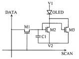
- FIG. 5shows the third embodiment of the present invention, which comprises a first transistor (switching transistor) M 1 , a storage capacitor C 1 , a second transistor (driving transistor) M 2 , a third transistor (driving transistor) M 3 and an OLED.
- the first transistorhas a gate terminal coupled to a scan signal SCAN and a drain terminal coupled to a data signal DATA.
- the first transistor M 1controls the transmission of data signal DATA according to the scan signal SCAN.
- the storage capacitor C 1has two terminals coupled to a source terminal of the first transistor M 1 and a reference node.
- the reference nodehas a second voltage V 2 .
- the second transistor M 2 and the third transistor M 3are connected in parallel.
- the second transistor M 2 and the third transistor M 3have gate terminals coupled to the source terminal of the first transistor M 1 and source terminals coupled to the reference node.
- the OLEDhas a cathode coupled to drain terminals of the second transistor M 2 and the third transistor M 3 and an anode coupled to a first voltage V 1 .
- the first voltage V 1exceeds the second voltage V 2 .
- the second transistor M 2 and the third transistor M 3control current through the OLED according to the data signal DATA.
- the second transistor M 2 and the third transistor M 3are an amorphous silicon thin film transistor (a-Si TFT), and equivalent channel width/length (W/L) ratios of the second transistor M 2 and the third transistor M 3 exceed 5.
- the third embodimentreduces the W/L ratio requirement by parallel connection.
- the relation between the amount N of the driving transistors and equivalent channel width/length (W/L) ratio Ris R ⁇ 10 N .
- the second voltage V 2is a ground or a low voltage
- the first voltageis a power supply voltage
- FIG. 5 bshows a fourth embodiment of the present invention, wherein the OLED is connected to the source terminals of the second transistor M 2 and the third transistor M 3 via the anode, and to the first voltage V 1 via the cathode.
- the drain terminals of the second transistor (driving transistor) M 2 and the third transistor (driving transistor) M 3are connected to the reference node.
- the second voltage V 2exceeds the first voltage V 1 .
- the present inventioncan also constitute display comprising the pixel structure disclosed.
- the present inventionutilizes a less complex TFT to control the signal of the active matrix OLED display, decreasing costs thereof.
Landscapes
- Engineering & Computer Science (AREA)
- Physics & Mathematics (AREA)
- Computer Hardware Design (AREA)
- General Physics & Mathematics (AREA)
- Theoretical Computer Science (AREA)
- Geometry (AREA)
- Microelectronics & Electronic Packaging (AREA)
- Electroluminescent Light Sources (AREA)
- Control Of El Displays (AREA)
- Control Of Indicators Other Than Cathode Ray Tubes (AREA)
Abstract
Description
- 1. Field of the Invention[0001]
- The present invention relates to an active matrix organic light-emitting diode (OLED) display and in particular to a less costly and easily manufactured active matrix OLED display.[0002]
- 2. Description of the Related Art[0003]
- Organic light-emitting diodes (OLED) are active lighting elements, which, when receiving a voltage, inject an electron into an organic semiconductor through a cathode, and into an electron hole through an anode. The electron and the electron hole form an electron-hole pair in an organic thin film, and produce photons by radiative recombination.[0004]
- Compared with a conventional inorganic LED, the OLED is easily formed on large panels. As well, displays utilizing OLEDs require no backlight module, such that process is simpler and costs are reduced.[0005]
- OLEDs can be applied to small panels such as those in personal digital assistant (PDA) or digital camera applications.[0006]
- In conventional OLED display, a pixel is formed by two thin film transistors (TFT). The first TFT switches the pixel, and the second TFT controls the power applied to the OLED. Two types of common TFTs are applied to OLED displays, amorphous silicon thin film transistor (a-Si TFT) and low-temperature Poli-silicon (LTPS) TFT. The carrier mobility of the LTPS TFT is 100 times that of a-Si TFT, such that the LTPS TFT can supply the OLED with sufficient current, making it a better choice as a control element of the active matrix OLED display. However, manufacture of the LTPS TFT is very complicated, lowering product reliability and increasing costs.[0007]
- The pixel structure of the present invention comprises a first transistor, a storage capacitor, a second transistor and an OLED. The first transistor has a gate terminal coupled to a scan signal and a drain terminal coupled to a data signal. The storage capacitor has two terminals coupled to a source terminal of the first transistor and a reference node, which has a second voltage. The second transistor has a gate terminal coupled to the source terminal of the first transistor and a source terminal coupled to the reference node. The OLED has a cathode coupled to a drain terminal of the second transistor and an anode coupled to a first voltage, higher than the second voltage. The second transistor is an amorphous silicon thin film transistor (a-Si TFT), and an equivalent channel width/length (W/L) ratio of the second transistor exceeds 10.[0008]
- The present invention can be more fully understood by reading the subsequent detailed description and examples with references made to the accompanying drawings, wherein:[0009]
- FIG. 1[0010]ashows the first embodiment of the present invention;
- FIG. 1[0011]bshows the second embodiment of the present invention;
- FIG. 2 shows electrical properties of the a-Si and LTPS TFTs;[0012]
- FIG. 3 shows the structure of the a-si TFT;[0013]
- FIG. 4 shows electrical properties of an a-Si TFT with an equivalent channel width/length (W/L) ratio greater than 10 and a common a-Si TFT;[0014]
- FIG. 5[0015]ashows the third embodiment of the present invention;
- FIG. 5[0016]bshows the fourth embodiment of the present invention.
- FIG. 1 shows a first example of the present invention. The pixel structure comprises a first transistor (switching transistor) M[0017]1, a storage capacitor C1, a second transistor (driving transistor) M2 and an organic light-emitting diode (OLED). The first transistor has a gate terminal coupled to a scan signal SCAN and a drain terminal coupled to a data signal DATA. The first transistor M1 controls the transmission of data signal DATA according to the scan signal SCAN. The storage capacitor C1 has two terminals coupled to a source terminal of the first transistor M1 and a reference node. The reference node has a second voltage V2. The second transistor M2 has a gate terminal coupled to the source terminal of the first transistor M1 and a source terminal coupled to the reference node. The OLED has a cathode coupled to a drain terminal of the second transistor M2 and an anode coupled to a first voltage V1. The first voltage V1 exceeds the second voltage V2. The second transistor controls the current through the OLED according to the data signal DATA. The second transistor M2 is an amorphous silicon thin film transistor (a-Si TFT), and an equivalent channel width/length (W/L) ratio of the second transistor M2 exceeds10.
- The second voltage V[0018]2 is a ground or a low voltage.
- The first voltage is a power supply voltage.[0019]
- FIG. 1[0020]bshows a second embodiment of the present invention, wherein the OLED is connected to the source terminal of the second transistor M2 via the anode, and connected to the first voltage V1 via the cathode. The drain terminal of the second transistor M2 is connected to the reference node. The second voltage V2 exceeds the first voltage V1.
- When a voltage of the scan signal SCAN received by the gate terminal of the first transistor M[0021]1 exceeds an active voltage of the first transistor M1, the first transistor M1 transmits the data signal DATA to the storage capacitor C1. Then, when a stored voltage Vg in the storage capacitor C1 exceeds an active voltage of the second transistor M2, the second transistor M2 transmits an actuation current through the OLED according to the stored voltage Vg. Thus, brightness of the OLED is controlled by the data signal DATA.
- Applied with the same voltage, the a-Si TFT transmits less current than the LTPS TFT transmits, however, by increasing an equivalent channel width/length (W/L) ratio of the a-Si TFT, sufficient actuation current is provided to actuate the OLED.[0022]
- Table 1 shows a simulation result of current needed to actuate display. As shown in Table 1, the highest current request for actuating the OLED is about 6.13 μA. Thus, if the a-Si TFT can supply a current with 6.13 μA, it can be applied in an active matrix OLED display.[0023]
TABLE 1 Current Required Light required brightness efficiency to Maximum brightness from OLED of OLED activate of display (cd/m2) (cd/m2) (cd/A) OLED (μA) White R 8 450 4 0.65 light G 6 900 15 0.34 applied B 150 4 0.22 in mobile phone display (60) White R 0 1687 4 6.13 light G 80 3374 15 3.3 applied B 0 562 4 2 in notebook display (300) - I[0025]Dis output current, μ carrier mobility, VGSinput voltage, Vththreshold voltage, W channel width, and L channel length. Accordingly, the output current can be raised by increasing carrier mobility, equivalent channel width/length (W/L) ratio, or input voltage. Because the carrier mobility of the a-Si TFT is fixed between 0.5-1, it is difficult to raise the output current by increasing carrier mobility, and raising input voltage hastens degradation of the a-Si TFT. Thus, the optimum method of raising output current is to increase the equivalent channel width/length (W/L) ratio. FIG. 3 shows a structure of an a-Si TFT, comprising a
substrate 12,source terminal 20,drain terminal 22,channel 24,gate isolation layer 16, andgate terminal 18. W is channel width and L channel length. In FIG. 4, when the equivalent channel width/length (W/L) ratio equals10, the a-Si TFT outputs a 6.13 μA current by inputting only 7 volt input voltage. As to current leakage, performance of the a-Si TFT is superior to an LTPS TFT. Thus, the a-Si TFT can be applied in an OLED display by raising the W/L above 10. The less costly a-Si TFT commensurately reduces the price of the active matrix OLED display. - Parallel connection of two driving transistors reduces the equivalent channel width/length (W/L) ratio requirement. FIG. 5 shows the third embodiment of the present invention, which comprises a first transistor (switching transistor) M[0026]1, a storage capacitor C1, a second transistor (driving transistor) M2, a third transistor (driving transistor) M3 and an OLED. The first transistor has a gate terminal coupled to a scan signal SCAN and a drain terminal coupled to a data signal DATA. The first transistor M1 controls the transmission of data signal DATA according to the scan signal SCAN. The storage capacitor C1 has two terminals coupled to a source terminal of the first transistor M1 and a reference node. The reference node has a second voltage V2. The second transistor M2 and the third transistor M3 are connected in parallel. The second transistor M2 and the third transistor M3 have gate terminals coupled to the source terminal of the first transistor M1 and source terminals coupled to the reference node. The OLED has a cathode coupled to drain terminals of the second transistor M2 and the third transistor M3 and an anode coupled to a first voltage V1. The first voltage V1 exceeds the second voltage V2. The second transistor M2 and the third transistor M3 control current through the OLED according to the data signal DATA. The second transistor M2 and the third transistor M3 are an amorphous silicon thin film transistor (a-Si TFT), and equivalent channel width/length (W/L) ratios of the second transistor M2 and the third transistor M3 exceed 5.
- The second voltage V[0028]2 is a ground or a low voltage, and the first voltage is a power supply voltage.
- FIG. 5[0029]bshows a fourth embodiment of the present invention, wherein the OLED is connected to the source terminals of the second transistor M2 and the third transistor M3 via the anode, and to the first voltage V1 via the cathode. The drain terminals of the second transistor (driving transistor) M2 and the third transistor (driving transistor) M3 are connected to the reference node. The second voltage V2 exceeds the first voltage V1.
- The present invention can also constitute display comprising the pixel structure disclosed.[0030]
- The present invention utilizes a less complex TFT to control the signal of the active matrix OLED display, decreasing costs thereof.[0031]
- While the invention has been described by way of example and in terms of the preferred embodiments, it is to be understood that the invention is not limited to the disclosed embodiments. To the contrary, it is intended to cover various modifications and similar arrangements (as would be apparent to those skilled in the art). Therefore, the scope of the appended claims should be accorded the broadest interpretation so as to encompass all such modifications and similar arrangements.[0032]


Claims (16)
1. A pixel structure of an active matrix organic light-emitting diode (OLED) display, comprising:
a first transistor having a gate terminal coupled to a scan signal and a drain terminal coupled to a data signal;
a storage capacitor having two terminals coupled to a source terminal of the first transistor and a reference node respectively, the reference node having a second voltage;
a second transistor having a gate terminal coupled to the source terminal of the first transistor and a source terminal coupled to the reference node; and
an OLED having a cathode coupled to a drain terminal of the second transistor and an anode coupled to a first voltage exceeding the second voltage;
wherein the second transistor is an amorphous silicon thin film transistor (a-Si TFT), and an equivalent channel width/length (W/L) ratio of the second transistor exceeds 10.
2. The pixel structure as claimed inclaim 1 , wherein the second voltage is a ground or a low voltage.
3. A pixel structure of an active matrix organic light-emitting diode (OLED) display, comprising:
a switching transistor having a gate terminal coupled to a scan signal and a drain terminal coupled to a data signal;
a storage capacitor having two terminals coupled to a source terminal of the switching transistor and a reference node respectively, the reference node having a second voltage;
a plurality of driving transistors connected in parallel, each having a gate terminal coupled to the source terminal of the switching transistor, a source terminal coupled to the reference node, and a drain terminal; and
an OLED having a cathode coupled to the drain terminals of the driving transistor and an anode coupled to a first voltage exceeding the second voltage;
wherein the driving transistors are amorphous silicon thin film transistors (a-Si TFT), wherein the relationship between an equivalent channel width/length (W/L) ratio R of the driving transistor and the number of driving transistors N is

4. The pixel structure as claimed inclaim 3 , wherein the second voltage is a ground or a low voltage.
5. An active matrix organic light-emitting diode (OLED) display, comprising:
a panel, comprising a plurality of pixels, each comprising a first transistor having a gate terminal coupled to a scan signal and a drain terminal coupled to a data signal; a storage capacitor having two terminals coupled to a source terminal of the first transistor and a reference node respectively, the reference node having a second voltage; a second transistor having a gate terminal coupled to the source terminal of the first transistor and a source terminal coupled to the reference node; and an OLED having a cathode coupled to a drain terminal of the second transistor and an anode coupled to a first voltage exceeding the second voltage; wherein the second transistor is an amorphous silicon thin film transistor (a-Si TFT), and an equivalent channel width/length (W/L) ratio of the second transistor exceeds 10.
6. The active matrix OLED display as claimed inclaim 5 , wherein the second voltage is a ground or a low voltage.
7. An active matrix organic light-emitting diode (OLED) display, comprising:
a panel, comprising a plurality of pixels, each comprising a switching transistor having a gate terminal coupled to a scan signal and a drain terminal coupled to a data signal; a storage capacitor having two terminals coupled to a source terminal of the switching transistor and a reference node respectively, the reference node having a second voltage; a plurality of driving transistors connected in parallel, each having a gate terminal coupled to the source terminal of the switching transistor, a source terminal coupled to the reference node and a drain terminal; and an OLED having a cathode coupled to the drain terminals of the driving transistor and an anode coupled to a first voltage exceeding the second voltage; wherein the driving transistors are amorphous silicon thin film transistors (a-Si TFT), wherein the relationship between an equivalent channel width/length (W/L) ratio R of the driving transistor and the number of driving transistors N is

8. The active matrix OLED display as claimed inclaim 7 , wherein the second voltage is a ground or a low voltage.
9. A pixel structure of an active matrix organic light-emitting diode (OLED) display, comprising:
a first transistor having a gate terminal coupled to a scan signal and a drain terminal coupled to a data signal;
a storage capacitor having two terminals coupled to a source terminal of the first transistor and a reference node respectively, the reference node having a second voltage;
a second transistor having a gate terminal coupled to the source terminal of the first transistor and a drain terminal coupled to the reference node; and
an OLED having an anode coupled to a source terminal of the second transistor and a cathode coupled to a first voltage less than the second voltage;
wherein the second transistor is an amorphous silicon thin film transistor (a-Si TFT), and an equivalent channel width/length (W/L) ratio of the second transistor exceeds10.
10. The pixel structure as claimed inclaim 9 , wherein the second voltage is a high voltage.
11. A pixel structure of an active matrix organic light-emitting diode (OLED) display, comprising:
a switching transistor having a gate terminal coupled to a scan signal and a drain terminal coupled to a data signal;
a storage capacitor having two terminals coupled to a source terminal of the switching transistor and a reference node respectively, the reference node having a second voltage;
a plurality of driving transistors connected in parallel, each having a gate terminal coupled to the source terminal of the switching transistor, a drain terminal coupled to the reference node, and a source terminal; and
an OLED having an anode coupled to the source terminals of the driving transistor and a cathode coupled to a first voltage less than the second voltage;
wherein the driving transistors are amorphous silicon thin film transistors (a-Si TFT), and the relationship between an equivalent channel width/length (W/L) ratio R of the driving transistor and the number of driving transistors N is

12. The pixel structure as claimed inclaim 11 , wherein the second voltage is a ground or a high voltage.
13. An active matrix organic light-emitting diode (OLED) display, comprising:
a panel, comprising a plurality of pixels, each comprising a first transistor having a gate terminal coupled to a scan signal and a drain terminal coupled to a data signal; a storage capacitor having two terminals coupled to a source terminal of the first transistor and a reference node respectively, the reference node having a second voltage; a second transistor having a gate terminal coupled to the source terminal of the first transistor and a drain terminal coupled to the reference node; and an OLED having an anode coupled to a source terminal of the second transistor and a cathode coupled to a first voltage less than the second voltage; wherein the second transistor is an amorphous silicon thin film transistor (a-Si TFT), and an equivalent channel width/length (W/L) ratio of the second transistor exceeds 10.
14. The active matrix OLED display as claimed inclaim 13 , wherein the second voltage is a high voltage.
15. An active matrix organic light-emitting diode (OLED) display, comprising:
a panel, comprising a plurality of pixels, each comprising a switching transistor having a gate terminal coupled to a scan signal and a drain terminal coupled to a data signal; a storage capacitor having two terminals coupled to a source terminal of the switching transistor and a reference node respectively, the reference node having a second voltage; a plurality of driving transistors connected in parallel, each having a gate terminal coupled to the source terminal of the switching transistor, a drain terminal coupled to the reference node, and a source terminal; and an OLED having an anode coupled to the source terminals of the driving transistor and a cathode coupled to a first voltage less than the second voltage; wherein the driving transistors are amorphous silicon thin film transistors (a-Si TFT), and the relationship between an equivalent channel width/length (W/L) ratio R of the driving transistor and the number of driving transistors N is

16. The active matrix OLED display as claimed inclaim 15 , wherein the second voltage is a high voltage.
Applications Claiming Priority (2)
| Application Number | Priority Date | Filing Date | Title |
|---|---|---|---|
| TW92115178 | 2003-06-05 | ||
| TW092115178ATW200428688A (en) | 2003-06-05 | 2003-06-05 | Organic light-emitting display and its pixel structure |
Publications (2)
| Publication Number | Publication Date |
|---|---|
| US20040246209A1true US20040246209A1 (en) | 2004-12-09 |
| US7253815B2 US7253815B2 (en) | 2007-08-07 |
Family
ID=33488656
Family Applications (1)
| Application Number | Title | Priority Date | Filing Date |
|---|---|---|---|
| US10/797,160Active2025-11-09US7253815B2 (en) | 2003-06-05 | 2004-03-10 | OLED display and pixel structure thereof |
Country Status (2)
| Country | Link |
|---|---|
| US (1) | US7253815B2 (en) |
| TW (1) | TW200428688A (en) |
Cited By (20)
| Publication number | Priority date | Publication date | Assignee | Title |
|---|---|---|---|---|
| US20060061525A1 (en)* | 2004-09-21 | 2006-03-23 | Kim Eun-Ah | Organic electroluminescent display device having plurality of driving transistors and plurality of anodes or cathodes per pixel |
| US20070108443A1 (en)* | 2005-11-14 | 2007-05-17 | Kim Eun A | Organic light emitting display device |
| US20080030433A1 (en)* | 2006-08-04 | 2008-02-07 | Ritdisplay Corporation | Driving circuit |
| US20080030451A1 (en)* | 2006-08-04 | 2008-02-07 | Ritdisplay Corporation | Active matrix organic electro-luminescence display panel |
| US20080030443A1 (en)* | 2006-08-03 | 2008-02-07 | Sony Corporation | Display device and electronic equipment |
| US20080122755A1 (en)* | 2006-11-24 | 2008-05-29 | Ritdisplay Corporation | Active matrix organic electro-luminescence display panel and fabrication method thereof |
| US20080143653A1 (en)* | 2006-12-15 | 2008-06-19 | Semiconductor Energy Laboratory Co., Ltd. | Semiconductor device and driving method thereof |
| US20080238328A1 (en)* | 2007-03-26 | 2008-10-02 | Yun Seung Shin | Light emitting pixel and apparatus for driving the same |
| CN100451795C (en)* | 2006-11-13 | 2009-01-14 | 友达光电股份有限公司 | Pixel structure |
| US20100096638A1 (en)* | 2008-10-21 | 2010-04-22 | Byoung Kwon Choo | Thin film transistor substrate, method of manufacturing the same, and display apparatus having the same |
| US20100123700A1 (en)* | 2008-11-15 | 2010-05-20 | Seung-Tae Kim | Organic electroluminescent display device and method of driving the same |
| US20150097762A1 (en)* | 2013-10-07 | 2015-04-09 | Samsung Display Co., Ltd. | Pixel and organic light emitting display using the same |
| US20150187269A1 (en)* | 2013-12-30 | 2015-07-02 | Shanghai Tianma AM-OLED Co., Ltd | Organic light-emitting diode pixel circuit, display panel and display device |
| US20170047003A1 (en)* | 2015-08-12 | 2017-02-16 | Samsung Display Co., Ltd. | Display device |
| TWI587271B (en)* | 2012-05-18 | 2017-06-11 | 半導體能源研究所股份有限公司 | Pixel circuit, display device, and electronic device |
| US9955097B2 (en) | 2005-06-02 | 2018-04-24 | Sony Corporation | Semiconductor image sensor module and method of manufacturing the same |
| CN111292687A (en)* | 2020-02-20 | 2020-06-16 | 京东方科技集团股份有限公司 | Pixel drive circuit, pixel structure and display panel |
| CN114937436A (en)* | 2022-06-30 | 2022-08-23 | 天马微电子股份有限公司 | Display panel and display device |
| CN115862518A (en)* | 2022-12-29 | 2023-03-28 | Tcl华星光电技术有限公司 | Gate drive circuit and display panel |
| US20250124868A1 (en)* | 2022-07-13 | 2025-04-17 | Beijing Boe Technology Development Co., Ltd. | Semiconductor substrate and driving method therefor, and semiconductor display apparatus |
Families Citing this family (2)
| Publication number | Priority date | Publication date | Assignee | Title |
|---|---|---|---|---|
| TWI488348B (en)* | 2012-05-24 | 2015-06-11 | Au Optronics Corp | Pixel circuit of the light emitting diode display, the driving method thereof and the light emitting diode display |
| KR101967407B1 (en)* | 2012-10-08 | 2019-04-10 | 삼성디스플레이 주식회사 | Organic light emitting diode display |
Citations (12)
| Publication number | Priority date | Publication date | Assignee | Title |
|---|---|---|---|---|
| US5463335A (en)* | 1992-10-30 | 1995-10-31 | International Business Machines Corporation | Power up detection circuits |
| US6097179A (en)* | 1999-03-08 | 2000-08-01 | Texas Instruments Incorporated | Temperature compensating compact voltage regulator for integrated circuit device |
| US20010022565A1 (en)* | 2000-03-10 | 2001-09-20 | Hajime Kimura | Electronic device and method of driving electronic device |
| US20020135312A1 (en)* | 2001-03-22 | 2002-09-26 | Jun Koyama | Light emitting device, driving method for the same and electronic apparatus |
| US20030107565A1 (en)* | 2001-11-20 | 2003-06-12 | International Business Machines Corporation | Active matrix oled voltage drive pixel circuit |
| US20030146912A1 (en)* | 2002-02-04 | 2003-08-07 | Au Optronics Corp. | Display driving circuit |
| US20030156101A1 (en)* | 2001-10-19 | 2003-08-21 | Lechevalier Robert | Adaptive control boost current method and apparatus |
| US20030197666A1 (en)* | 2002-04-17 | 2003-10-23 | Hajime Akimoto | Image display device |
| US20030205708A1 (en)* | 2002-05-01 | 2003-11-06 | Au Optronics Corp | Active matrix organic light emitting display and method of forming the same |
| US20030234392A1 (en)* | 2002-06-25 | 2003-12-25 | Nein-Hui Kung | Active matrix organic light emitting diode display pixel structure |
| US6879110B2 (en)* | 2000-07-27 | 2005-04-12 | Semiconductor Energy Laboratory Co., Ltd. | Method of driving display device |
| US20060027807A1 (en)* | 2001-02-16 | 2006-02-09 | Arokia Nathan | Pixel current driver for organic light emitting diode displays |
Family Cites Families (4)
| Publication number | Priority date | Publication date | Assignee | Title |
|---|---|---|---|---|
| JP2804063B2 (en) | 1989-02-15 | 1998-09-24 | 株式会社日立製作所 | Thin film transistor, active matrix circuit substrate using the transistor, and image display device |
| US6157356A (en) | 1996-04-12 | 2000-12-05 | International Business Machines Company | Digitally driven gray scale operation of active matrix OLED displays |
| JP2000221903A (en) | 1999-01-29 | 2000-08-11 | Sanyo Electric Co Ltd | Electro-luminescence display device |
| JP3757797B2 (en) | 2001-01-09 | 2006-03-22 | 株式会社日立製作所 | Organic LED display and driving method thereof |
- 2003
- 2003-06-05TWTW092115178Apatent/TW200428688A/ennot_activeIP Right Cessation
- 2004
- 2004-03-10USUS10/797,160patent/US7253815B2/enactiveActive
Patent Citations (14)
| Publication number | Priority date | Publication date | Assignee | Title |
|---|---|---|---|---|
| US5463335A (en)* | 1992-10-30 | 1995-10-31 | International Business Machines Corporation | Power up detection circuits |
| US6097179A (en)* | 1999-03-08 | 2000-08-01 | Texas Instruments Incorporated | Temperature compensating compact voltage regulator for integrated circuit device |
| US20010022565A1 (en)* | 2000-03-10 | 2001-09-20 | Hajime Kimura | Electronic device and method of driving electronic device |
| US6879110B2 (en)* | 2000-07-27 | 2005-04-12 | Semiconductor Energy Laboratory Co., Ltd. | Method of driving display device |
| US7158104B2 (en)* | 2000-07-27 | 2007-01-02 | Semiconductor Energy Laboratory Co., Ltd. | Method of driving display device |
| US20060027807A1 (en)* | 2001-02-16 | 2006-02-09 | Arokia Nathan | Pixel current driver for organic light emitting diode displays |
| US20020135312A1 (en)* | 2001-03-22 | 2002-09-26 | Jun Koyama | Light emitting device, driving method for the same and electronic apparatus |
| US20030156101A1 (en)* | 2001-10-19 | 2003-08-21 | Lechevalier Robert | Adaptive control boost current method and apparatus |
| US20030107565A1 (en)* | 2001-11-20 | 2003-06-12 | International Business Machines Corporation | Active matrix oled voltage drive pixel circuit |
| US20030146912A1 (en)* | 2002-02-04 | 2003-08-07 | Au Optronics Corp. | Display driving circuit |
| US20030197666A1 (en)* | 2002-04-17 | 2003-10-23 | Hajime Akimoto | Image display device |
| US20030205708A1 (en)* | 2002-05-01 | 2003-11-06 | Au Optronics Corp | Active matrix organic light emitting display and method of forming the same |
| US20040232420A1 (en)* | 2002-05-01 | 2004-11-25 | Au Optronics Corp. | Active matrix organic light emitting display and method of forming the same |
| US20030234392A1 (en)* | 2002-06-25 | 2003-12-25 | Nein-Hui Kung | Active matrix organic light emitting diode display pixel structure |
Cited By (51)
| Publication number | Priority date | Publication date | Assignee | Title |
|---|---|---|---|---|
| US20060061525A1 (en)* | 2004-09-21 | 2006-03-23 | Kim Eun-Ah | Organic electroluminescent display device having plurality of driving transistors and plurality of anodes or cathodes per pixel |
| US9202853B2 (en) | 2004-09-21 | 2015-12-01 | Samsung Display Co., Ltd. | Organic electroluminescent display device having plurality of driving transistors and plurality of anodes or cathodes per pixel |
| US8441420B2 (en)* | 2004-09-21 | 2013-05-14 | Samsung Display Co., Ltd. | Organic electroluminescent display device having plurality of driving transistors and plurality of anodes or cathodes per pixel |
| US11722800B2 (en) | 2005-06-02 | 2023-08-08 | Sony Group Corporation | Semiconductor image sensor module and method of manufacturing the same |
| US11228728B2 (en) | 2005-06-02 | 2022-01-18 | Sony Group Corporation | Semiconductor image sensor module and method of manufacturing the same |
| US10645324B2 (en) | 2005-06-02 | 2020-05-05 | Sony Corporation | Semiconductor image sensor module and method of manufacturing the same |
| US10594972B2 (en) | 2005-06-02 | 2020-03-17 | Sony Corporation | Semiconductor image sensor module and method of manufacturing the same |
| US10129497B2 (en) | 2005-06-02 | 2018-11-13 | Sony Corporation | Semiconductor image sensor module and method of manufacturing the same |
| US9955097B2 (en) | 2005-06-02 | 2018-04-24 | Sony Corporation | Semiconductor image sensor module and method of manufacturing the same |
| US20070108443A1 (en)* | 2005-11-14 | 2007-05-17 | Kim Eun A | Organic light emitting display device |
| US8338832B2 (en) | 2005-11-14 | 2012-12-25 | Samsung Display Co., Ltd. | Organic light emitting display device |
| US20110012876A1 (en)* | 2006-08-03 | 2011-01-20 | Sony Corporation | Display device and electronic equipment |
| US9406258B2 (en)* | 2006-08-03 | 2016-08-02 | Sony Corporation | Display device and electronic equipment |
| US11151938B2 (en)* | 2006-08-03 | 2021-10-19 | Sony Group Corporation | Display device and electronic equipment |
| US20080030443A1 (en)* | 2006-08-03 | 2008-02-07 | Sony Corporation | Display device and electronic equipment |
| US8217878B2 (en)* | 2006-08-03 | 2012-07-10 | Sony Corporation | Display device and electronic equipment |
| US10573233B2 (en)* | 2006-08-03 | 2020-02-25 | Sony Corporation | Display device and electronic equipment |
| US9870736B2 (en)* | 2006-08-03 | 2018-01-16 | Sony Corporation | Display device and electronic equipment |
| US9620059B2 (en) | 2006-08-03 | 2017-04-11 | Sony Corporation | Display device and electronic equipment |
| US7825879B2 (en)* | 2006-08-03 | 2010-11-02 | Sony Corporation | Display device and electronic equipment |
| US20150364086A1 (en)* | 2006-08-03 | 2015-12-17 | Sony Corporation | Display device and electronic equipment |
| US8692744B2 (en)* | 2006-08-03 | 2014-04-08 | Sony Corporation | Display device and electronic equipment |
| US8773335B2 (en) | 2006-08-03 | 2014-07-08 | Sony Corporation | Display device and electronic equipment |
| US9129553B2 (en) | 2006-08-03 | 2015-09-08 | Sony Corporation | Display device and electronic equipment |
| US20080030433A1 (en)* | 2006-08-04 | 2008-02-07 | Ritdisplay Corporation | Driving circuit |
| US20080030451A1 (en)* | 2006-08-04 | 2008-02-07 | Ritdisplay Corporation | Active matrix organic electro-luminescence display panel |
| US7935959B2 (en)* | 2006-08-04 | 2011-05-03 | Ritdisplay Corporation | Active matrix organic electro-luminescence display panel |
| CN100451795C (en)* | 2006-11-13 | 2009-01-14 | 友达光电股份有限公司 | Pixel structure |
| US20080122755A1 (en)* | 2006-11-24 | 2008-05-29 | Ritdisplay Corporation | Active matrix organic electro-luminescence display panel and fabrication method thereof |
| US8284125B2 (en)* | 2006-11-24 | 2012-10-09 | Ritdisplay Corporation | Active matrix organic electro-luminescence display panel and fabrication method thereof |
| US20080143653A1 (en)* | 2006-12-15 | 2008-06-19 | Semiconductor Energy Laboratory Co., Ltd. | Semiconductor device and driving method thereof |
| US8477085B2 (en) | 2006-12-15 | 2013-07-02 | Semiconductor Energy Laboratory Co., Ltd. | Semiconductor device and driving method thereof |
| US20080238328A1 (en)* | 2007-03-26 | 2008-10-02 | Yun Seung Shin | Light emitting pixel and apparatus for driving the same |
| US7973483B2 (en)* | 2007-03-26 | 2011-07-05 | Samsung Electronics Co., Ltd. | Light emitting pixel and apparatus for driving the same |
| US20100096638A1 (en)* | 2008-10-21 | 2010-04-22 | Byoung Kwon Choo | Thin film transistor substrate, method of manufacturing the same, and display apparatus having the same |
| US8860032B2 (en)* | 2008-10-21 | 2014-10-14 | Samsung Display Co., Ltd. | Thin film transistor substrate, method of manufacturing the same, and display apparatus having the same which improve switching characteristics |
| US20100123700A1 (en)* | 2008-11-15 | 2010-05-20 | Seung-Tae Kim | Organic electroluminescent display device and method of driving the same |
| US9530353B2 (en) | 2008-11-15 | 2016-12-27 | Lg Display Co., Ltd. | Organic electroluminescent display device and method of driving the same |
| US8547305B2 (en)* | 2008-11-15 | 2013-10-01 | Lg Display Co., Ltd. | Organic electroluminescent display device and method of driving the same |
| TWI587271B (en)* | 2012-05-18 | 2017-06-11 | 半導體能源研究所股份有限公司 | Pixel circuit, display device, and electronic device |
| US20150097762A1 (en)* | 2013-10-07 | 2015-04-09 | Samsung Display Co., Ltd. | Pixel and organic light emitting display using the same |
| US20150187269A1 (en)* | 2013-12-30 | 2015-07-02 | Shanghai Tianma AM-OLED Co., Ltd | Organic light-emitting diode pixel circuit, display panel and display device |
| US9202414B2 (en)* | 2013-12-30 | 2015-12-01 | Shanghai Tianma AM-OLED Co., Ltd | Organic light-emitting diode pixel circuit, display panel and display device |
| US20170047003A1 (en)* | 2015-08-12 | 2017-02-16 | Samsung Display Co., Ltd. | Display device |
| US10861385B2 (en)* | 2015-08-12 | 2020-12-08 | Samsung Display Co., Ltd. | Display device including pixels with driving transistors that have different amounts of unit transistors |
| CN111292687A (en)* | 2020-02-20 | 2020-06-16 | 京东方科技集团股份有限公司 | Pixel drive circuit, pixel structure and display panel |
| US11869424B2 (en) | 2020-02-20 | 2024-01-09 | Boe Technology Group Co., Ltd. | Pixel driving circuit, pixel structure, and display panel |
| CN114937436A (en)* | 2022-06-30 | 2022-08-23 | 天马微电子股份有限公司 | Display panel and display device |
| US12236869B2 (en) | 2022-06-30 | 2025-02-25 | Tianma Microelectronics Co., Ltd. | Display panel and display device |
| US20250124868A1 (en)* | 2022-07-13 | 2025-04-17 | Beijing Boe Technology Development Co., Ltd. | Semiconductor substrate and driving method therefor, and semiconductor display apparatus |
| CN115862518A (en)* | 2022-12-29 | 2023-03-28 | Tcl华星光电技术有限公司 | Gate drive circuit and display panel |
Also Published As
| Publication number | Publication date |
|---|---|
| TWI302044B (en) | 2008-10-11 |
| US7253815B2 (en) | 2007-08-07 |
| TW200428688A (en) | 2004-12-16 |
Similar Documents
| Publication | Publication Date | Title |
|---|---|---|
| US7253815B2 (en) | OLED display and pixel structure thereof | |
| US11062652B1 (en) | Pixel circuit, driving method thereof, display panel and display device | |
| US10971067B1 (en) | AMOLED pixel driving circuit, driving method and terminal | |
| US10089929B2 (en) | Pixel driver circuit with load-balance in current mirror circuit | |
| US10872566B2 (en) | OLED pixel circuit, driving method for the OLED pixel circuit and display device | |
| US7872620B2 (en) | Pixel structure using voltage programming-type for active matrix organic light emitting device | |
| US8330680B2 (en) | Light-emitting display | |
| KR101239157B1 (en) | Semiconductor device, and display device, driving method and electronic apparatus thereof | |
| US7423638B2 (en) | Organic electroluminescent display, driving method and pixel circuit thereof | |
| KR101278205B1 (en) | Display device and driving method of display device | |
| US20150154907A1 (en) | Pixel driver circuit and pixel circuit having control circuit coupled to supply voltage | |
| US20020180671A1 (en) | Display device and method of driving the same | |
| US10714010B2 (en) | Pixel compensation circuit, method for driving the same, organic light-emitting diode display panel, and display device | |
| CN111754939B (en) | Pixel circuit, driving method thereof and display device | |
| JP4999351B2 (en) | Semiconductor device and display device | |
| US7615803B2 (en) | Method for manufacturing transistor and image display device using the same | |
| US20240395207A1 (en) | Pixel circuit, driving method and display apparatus | |
| US7006062B2 (en) | Driving circuit of display | |
| US20030234392A1 (en) | Active matrix organic light emitting diode display pixel structure | |
| CN114899213A (en) | Display panel and display device | |
| CN114038393A (en) | Pixel circuit and display panel | |
| US12230214B2 (en) | Array substrate, display panel and driving method of array substrate | |
| US20040246201A1 (en) | OLED display and pixel structure thereof | |
| US20050212448A1 (en) | Organic EL display and active matrix substrate | |
| CN1567412A (en) | Organic Light Emitting Display and Its Pixel Structure |
Legal Events
| Date | Code | Title | Description |
|---|---|---|---|
| AS | Assignment | Owner name:AU OPTRONICS CORP., TAIWAN Free format text:ASSIGNMENT OF ASSIGNORS INTEREST;ASSIGNOR:SUNG, CHIH-FENG;REEL/FRAME:015092/0140 Effective date:20040216 | |
| STCF | Information on status: patent grant | Free format text:PATENTED CASE | |
| FPAY | Fee payment | Year of fee payment:4 | |
| FPAY | Fee payment | Year of fee payment:8 | |
| MAFP | Maintenance fee payment | Free format text:PAYMENT OF MAINTENANCE FEE, 12TH YEAR, LARGE ENTITY (ORIGINAL EVENT CODE: M1553); ENTITY STATUS OF PATENT OWNER: LARGE ENTITY Year of fee payment:12 |