US20040245557A1 - Nonvolatile memory device comprising one switching device and one resistant material and method of manufacturing the same - Google Patents
Nonvolatile memory device comprising one switching device and one resistant material and method of manufacturing the sameDownload PDFInfo
- Publication number
- US20040245557A1 US20040245557A1US10/852,287US85228704AUS2004245557A1US 20040245557 A1US20040245557 A1US 20040245557A1US 85228704 AUS85228704 AUS 85228704AUS 2004245557 A1US2004245557 A1US 2004245557A1
- Authority
- US
- United States
- Prior art keywords
- data storage
- material layer
- storage material
- memory device
- voltage
- Prior art date
- Legal status (The legal status is an assumption and is not a legal conclusion. Google has not performed a legal analysis and makes no representation as to the accuracy of the status listed.)
- Granted
Links
Images


Classifications
- G—PHYSICS
- G11—INFORMATION STORAGE
- G11C—STATIC STORES
- G11C13/00—Digital stores characterised by the use of storage elements not covered by groups G11C11/00, G11C23/00, or G11C25/00
- G11C13/0002—Digital stores characterised by the use of storage elements not covered by groups G11C11/00, G11C23/00, or G11C25/00 using resistive RAM [RRAM] elements
- G11C13/0007—Digital stores characterised by the use of storage elements not covered by groups G11C11/00, G11C23/00, or G11C25/00 using resistive RAM [RRAM] elements comprising metal oxide memory material, e.g. perovskites
- G—PHYSICS
- G11—INFORMATION STORAGE
- G11C—STATIC STORES
- G11C11/00—Digital stores characterised by the use of particular electric or magnetic storage elements; Storage elements therefor
- G11C11/02—Digital stores characterised by the use of particular electric or magnetic storage elements; Storage elements therefor using magnetic elements
- G11C11/14—Digital stores characterised by the use of particular electric or magnetic storage elements; Storage elements therefor using magnetic elements using thin-film elements
- G11C11/15—Digital stores characterised by the use of particular electric or magnetic storage elements; Storage elements therefor using magnetic elements using thin-film elements using multiple magnetic layers
- H—ELECTRICITY
- H10—SEMICONDUCTOR DEVICES; ELECTRIC SOLID-STATE DEVICES NOT OTHERWISE PROVIDED FOR
- H10B—ELECTRONIC MEMORY DEVICES
- H10B63/00—Resistance change memory devices, e.g. resistive RAM [ReRAM] devices
- H10B63/20—Resistance change memory devices, e.g. resistive RAM [ReRAM] devices comprising selection components having two electrodes, e.g. diodes
- H—ELECTRICITY
- H10—SEMICONDUCTOR DEVICES; ELECTRIC SOLID-STATE DEVICES NOT OTHERWISE PROVIDED FOR
- H10B—ELECTRONIC MEMORY DEVICES
- H10B63/00—Resistance change memory devices, e.g. resistive RAM [ReRAM] devices
- H10B63/30—Resistance change memory devices, e.g. resistive RAM [ReRAM] devices comprising selection components having three or more electrodes, e.g. transistors
- H—ELECTRICITY
- H10—SEMICONDUCTOR DEVICES; ELECTRIC SOLID-STATE DEVICES NOT OTHERWISE PROVIDED FOR
- H10N—ELECTRIC SOLID-STATE DEVICES NOT OTHERWISE PROVIDED FOR
- H10N70/00—Solid-state devices having no potential barriers, and specially adapted for rectifying, amplifying, oscillating or switching
- H10N70/20—Multistable switching devices, e.g. memristors
- H—ELECTRICITY
- H10—SEMICONDUCTOR DEVICES; ELECTRIC SOLID-STATE DEVICES NOT OTHERWISE PROVIDED FOR
- H10N—ELECTRIC SOLID-STATE DEVICES NOT OTHERWISE PROVIDED FOR
- H10N70/00—Solid-state devices having no potential barriers, and specially adapted for rectifying, amplifying, oscillating or switching
- H10N70/801—Constructional details of multistable switching devices
- H10N70/821—Device geometry
- H10N70/826—Device geometry adapted for essentially vertical current flow, e.g. sandwich or pillar type devices
- H—ELECTRICITY
- H10—SEMICONDUCTOR DEVICES; ELECTRIC SOLID-STATE DEVICES NOT OTHERWISE PROVIDED FOR
- H10N—ELECTRIC SOLID-STATE DEVICES NOT OTHERWISE PROVIDED FOR
- H10N70/00—Solid-state devices having no potential barriers, and specially adapted for rectifying, amplifying, oscillating or switching
- H10N70/801—Constructional details of multistable switching devices
- H10N70/881—Switching materials
- H10N70/883—Oxides or nitrides
- H10N70/8833—Binary metal oxides, e.g. TaOx
- G—PHYSICS
- G11—INFORMATION STORAGE
- G11C—STATIC STORES
- G11C2213/00—Indexing scheme relating to G11C13/00 for features not covered by this group
- G11C2213/30—Resistive cell, memory material aspects
- G11C2213/32—Material having simple binary metal oxide structure
- G—PHYSICS
- G11—INFORMATION STORAGE
- G11C—STATIC STORES
- G11C2213/00—Indexing scheme relating to G11C13/00 for features not covered by this group
- G11C2213/70—Resistive array aspects
- G11C2213/79—Array wherein the access device being a transistor
Definitions
- the present inventionrelates to a nonvolatile memory, and more particularly, to a nonvolatile memory device comprising one transistor and one resistant material in which data is written and a method of manufacturing the nonvolatile memory device.
- An example of a conventional memory device that consists of one transistor and one resistant materialis a parameter random access memory (PRAM).
- PRAMparameter random access memory
- the resistant material used in the PRAMis a calcogenide material.
- the calcogenide materialmay be in an amorphous or crystalline state depending on a manufacturing temperature.
- the resistance of the calcogenide materialis high when it is amorphous and is low when it is crystalline.
- the PRAMis a nonvolatile memory device that reads and writes data by changing the state of the calcogenide resistant material.
- the present inventionprovides a nonvolatile memory device having one switching device, for example, a transistor (Tr) or diode, and one resistant material, and a method of manufacturing the nonvolatile memory device which can be mass produced at lower production costs.
- a memory characteristic of the resistant materialdoes not directly influence the degree of integration of the memory device.
- a nonvolatile memory devicecomprising a transistor and a data storage unit connected to a drain of the transistor, wherein the data storage unit includes a data storage material layer.
- the data storage material layershows a first resistance characteristic in a first voltage range and a second resistance characteristic in a second voltage range. The first voltage range differs from the second voltage range, and the first resistance characteristic differs from the second resistance characteristic.
- An upper electrode and a lower electrodemay be formed on the upper and lower surfaces of the data storage material layer, respectively.
- An interlayer insulating layermay be formed between the lower electrode and the substrate, a contact hole that exposes the drain is formed in the interlayer insulating layer, and the contact hole may be filled with a conductive plug.
- the data storage material layermay be a transition metal oxide layer whose resistance dramatically increases in a predetermined voltage range.
- a nonvolatile memory devicecomprising a diode with a switching function and a data storage unit connected to the diode, wherein the data storage unit includes a data storage material layer, which is the same in the above description.
- a method of manufacturing a nonvolatile memory devicecomprising a substrate, a transition formed on the substrate, and a data storage unit connected to a drain of the transistor, the method comprising: sequentially forming a lower electrode, a data storage material layer, and an upper electrode to form the data storage unit, wherein the data storage material layer is formed of a material layer having different resistance characteristics in different voltage ranges.
- the material layermay be formed of a transition metal oxide layer whose resistance dramatically increases in the voltage range.
- a method of manufacturing a nonvolatile memory devicecomprising: forming a diode on a substrate; and forming a data storage unit connected to the diode on the substrate, wherein the data storage unit is formed by sequentially forming a lower electrode connected to the diode, a data storage material layer, and an upper electrode.
- the data storage material layermay be formed of a material layer having different resistance characteristics in different voltage ranges.
- the data storage material layeris the same as described above.
- the conventional DRAM manufacturing processcan be used since the transition metal oxide layer is used as the resistant material.
- productivity increases and production costsare lowered.
- the memory characteristic of the resistant materialdoes not change, even though its size is reduced due to higher integration density, since the data is read and written using changes in resistance of the resistant material.
- data written to the resistant material layercan be non-destructively read, the resistant material remains in the same state as before data reading, and an operation voltage is lowered. Thus, after data is read, a restoring process is not required.
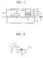
- FIG. 1is a cross-section of a nonvolatile memory device according to an embodiment of the present invention
- FIG. 2is a circuit diagram of the nonvolatile memory device of FIG. 1;
- FIG. 3is a cross-sectional view illustrating a variation of the non-memory device shown in FIG. 1 according to the present invention
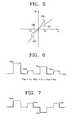
- FIG. 4is a graph illustrating voltage-current characteristics when a data storage material layer is an NiO layer in the nonvolatile memory device of FIG. 1;
- FIG. 5is a graph illustrating voltage-current characteristics when a data storage material layer is a TiO 2 layer in the nonvolatile memory device of FIG. 1;
- FIG. 6is a drawing illustrating a voltage pulse applied to the nonvolatile memory device of FIG. 1 when a data storage material layer is an NiO layer;
- FIG. 7illustrates a voltage pulse applied to the nonvolatile memory device of FIG. 1 when a data storage material layer is a TiO 2 layer;
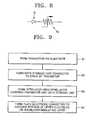
- FIG. 8is a circuit diagram illustrating a case where a transistor is replaced with a diode in the circuit of FIG. 2;
- FIG. 9is a block diagram illustrating a method of manufacturing the nonvolatile memory device of FIG. 1 according to an order of a process performed.
- FIG. 1is a cross-section of a nonvolatile memory device according to an embodiment of the present invention.
- a nonvolatile memory device having one transistor and one resistant materialincludes a substrate 40 , a transistor which is formed on the substrate 40 , and a data storage unit S which is connected to a portion of the transistor.
- the transistoris formed on an upper surface of the substrate 40 and includes a source 42 and a drain 44 doped with conductive impurities, and gate stacking materials 48 and 50 on a channel 46 between the source 42 and the drain 44 .
- the gate stacking materials 48 and 50consist of a gate insulating layer 48 and a gate electrode 50 .
- the data storage unit Sis formed on the drain 44 .
- the data storage unit Sincludes a lower electrode 52 directly contacting the drain 44 , a data storage material layer 54 stacked on the lower electrode 52 , and an upper electrode 56 stacked on the data storage material layer 54 .
- the data storage material layer 54is a variable resistant material layer in which resistance is changed according to a size and direction of voltage or current pulse.
- the variable resistant material layer that can be used as the data storage material 54is preferable to be a transition metal oxide layer such as NiO, V 2 O 5 , ZnO, Nb 2 O 5 , TiO 2 , WO 3 , CoO layers etc.
- the transition metal oxide layerhas a noticeable characteristic. That is, if a specific voltage or current value is applied to the transition metal oxide layer and thus the transition metal oxide layer has the specific value, the transition metal oxide layer maintains the specific value until a new specific value is applied. This characteristic of the transition metal oxide layer will be explained in detail later.
- An interlayer insulating layer 60 covering the transistor surrounding the data storage unit Sis formed on the substrate 40 .
- a section of the interlayer insulating layer 60 formed on the upper electrode 56is removed to expose an upper surface of the upper electrode 56 .
- a plate electrode 58which is stacked on the interlayer insulating layer 60 , is connected to the front of the exposed surface of the upper electrode 56 .
- the plate electrode 58 and the upper electrode 56may be formed of the same material.
- a current amplifier 61is connected to the drain 44 and senses and amplifies a drain current Id.
- FIG. 2is a circuit diagram of the nonvolatile memory device of FIG. 1.
- Trdenotes the transistor
- Rvdenotes a changeable resistant material corresponding to the data storage material layer 54 .
- FIG. 3is a cross-sectional view of a variation of the nonvolatile memory device shown in FIG. 1 according to the present invention.
- a first interlayer insulating layer 62 covering a source 42 , gate stacking materials 48 and 50 , and a drain 44is formed on a substrate 40 and has a flat upper surface.
- a contact hole h 1is formed in the first interlayer insulating layer 62 .
- the drain 44is exposed through the contact hole h 1 .
- the contact hole h 1is filled with a conductive plug 64 .
- the data storage unit Sis formed on the first interlayer insulating layer 62 covering the conductive plug 64 .
- a second interlayer insulating layer 66 covering the data storage unit Sis formed on the first interlayer insulating layer 62 .
- a via hole h 2is formed in the second interlayer insulating 66 such that the upper electrode 56 of the data storage unit S is exposed. where an upper electrode 56 of the data storage unit S is exposed.
- a plate electrode 58 filling the via hole h 2is formed on the second interlayer insulating layer 66 .
- the elements of the data storage unit Smay be not a stacked type.
- the lower electrode 52 of the data storage unit Smay have a cylindrical shape and the data storage material layer 54 may be formed on the surface of the lower electrode 52 .
- the lower electrode 52may be a columnar shape and the data storage material layer 54 may be formed on the upper surface of the lower electrode 52 .
- FIG. 4is a graph illustrating current-voltage characteristic of the data storage unit S when the data storage material layer 54 is an NiO layer
- FIG. 5is a graph illustrating current-voltage characteristic of the data storage unit S when the data storage material layer 54 is a TiO 2 layer.
- a horizontal axisindicates a voltage applied to the data storage unit S and a vertical axis indicates a drain current Id flowing between the source 42 and the drain 44 .
- a first graph G 1illustrates a case where the resistance of the data storage unit S, i.e., the resistance of the data storage material layer 54 , is lowered
- a second graph G 2illustrates a case where the resistance of the data storage material layer 54 has an increased value.
- the drain current Idis changed in proportional to the voltage applied to the data storage material layer 54 .
- V 1 >0the voltage applied to the data storage material layer 54 reaches a first voltage V 1 (V 1 >0)
- V 1first voltage
- V 2second voltage
- the resistance of the data storage material 54is dramatically while a voltage in the range of ⁇ V (V 1 -V 2 ) is applied to the data storage material layer 54 .
- the change of the drain current Idis the same as the change occurring when the first voltage V 1 is applied to the data storage material 54 .
- the change of the drain current Id of the data storage material layer 54is proportional to the applied voltage and is the same as when a lower voltage than the first voltage V 1 is applied thereto.
- the current of the data storage material layer 54varies depending on a voltage applied thereto, i.e., whether the voltage applied thereto is greater or smaller than the first voltage V 1 .
- the current measured at the predetermined voltage in the second caseis much less than that measured in the second case.
- the resistanceis much larger in the second case. This means that these two different currents can be measured from the data storage material layer 54 at a predetermined voltage smaller than the first voltage V 1 .
- the two current valuesrespectively correspond to data “0” and “1” written in the data storage material layer 54 .
- the first casecorresponds to data “1” being stored in the data storage material layer 54 and the second case corresponds to data “0” being stored in the data storage material layer 54 .
- the data values “0” and “1” for the first and second casesare optionally designated. That is, the first case may corresponding to data “0” being stored in the data storage material layer 54 and the second case may correspond to data “1” being stored in the data storage material layer 54 .
- the voltage-current characteristics of the data storage material layer 54differ from the voltage-current characteristics illustrated in FIG. 4.
- third and fifth graphs G 3 and G 5illustrate voltage-current characteristics when a negative voltage, that is, a voltage smaller than a fifth voltage V 5 (
- Fourth and sixth graphs G 4 and G 6illustrate voltage-current characteristics when a positive voltage, that is, one larger than a fourth voltage V 4 (V>V 4 >0), is applied to the data storage unit S and the resistance of the data storage material layer 54 dramatically increases.
- the voltage-current characteristics of the data storage material layer 54become those illustrated in the fourth graph G 4 when the voltage is positive and become those illustrated in the sixth graph G 6 when the voltage is negative.
- the data storage material layer 54maintains a high resistance until the fifth voltage V 5 is applied to the data storage unit S (hereinafter, this is called the third case).
- the fourth caseAfter a voltage smaller than the fifth voltage V 5 is applied to the data storage unit S, the voltage-current characteristics of the data storage material layer 54 become those illustrated in the fifth graph G 5 when the voltage is negative and those illustrated in the third graph G 3 when the voltage is positive. Thus, after a voltage smaller than the fifth voltage V 5 is applied to the data storage unit S, the data storage material layer 54 maintains a low resistance until the fourth voltage V 4 is applied to the data storage unit S (hereinafter, this is called the fourth case).
- the data storage material layer 54has two different currents (or resistances) in the range between the fifth voltage V 5 and the fourth voltage V 4 . This means that the data storage material layer 54 has the two different states in the above voltage range and one of the two different states may correspond to data “1” and the other may correspond to data “0” being stored in the data storage material layer 54 .
- the two states of the data storage material layer 54are determined as a voltage larger than the fourth voltage V 4 or smaller than the fifth voltage V 5 is applied to the data storage unit S. However, since the voltage applied to the data storage material layer 54 to detect these states is smaller than the fourth voltage V 4 or larger than the fifth voltage V 5 , the data storage material layer 54 maintains its initial state even after the state is detected. That is, data stored in the data storage material layer 54 is maintained even after the pertinent data is read.
- FIGS. 6 and 7illustrate examples of voltage pulses applied to the data storage unit S to write data in the data storage material layer 54 and read or erase the data written in the data storage material layer 54 .
- FIG. 6illustrates a voltage pulse applied to the data storage material layer 54 when it is a NiO layer
- FIG. 7illustrates a voltage pulse applied to the data storage material layer 54 when it is a TiO 2 layer.
- a second write voltage pulse V W2is applied to the data storage material layer 54 in order to write data, for example “1”, in the data storage material layer 54 .
- the second write voltage pulse V W2has a value corresponding to the third voltage V 3 of FIG. 4.
- a third read voltage pulse V R3is applied to the data storage material layer 54 to read the data “1” stored in the data storage material layer 54 .
- the third read voltage pulse V R3has a voltage that is lower than the first voltage V 1 of FIG. 4.
- a third write voltage pulse V E2is applied to the data storage material layer 54 in order to write data, for example “0”, in the data storage material layer 54 .
- the third write voltage pulse V E2has a voltage between the first and second voltages V 1 and V 2 . Therefore, when the third write voltage pulse V E2 , that is smaller than the second write voltage pulse V W2 , is applied to the data storage material layer 54 , the resistance of the data storage material layer 54 dramatically increases (see FIG. 4).
- the data storage material layer 54remains in this state when a voltage pulse applied to the data storage material layer 54 is lower than the first voltage V 1 (see the second graph G 2 of FIG. 4).
- a fourth read voltage pulse V R4is applied to the data storage material layer 54 to read the data “0” from the data storage material layer 54 .
- the fourth read voltage pulse V R4has a voltage that is lower than the first voltage V 1 of FIG. 4.
- the current measured from the data storage material layer 54is a lot smaller than the current measured when the data “1” is read.
- the data stored in the data storage material layer 54is erased by simply applying a voltage pulse that has an opposite polarity to one applied when writing the data to the data storage unit S.
- a first write voltage pulse V W1is applied to the data storage material layer 54 in order to write a predetermined data, for example “1”, in the data storage material layer 54 .
- a first read voltage pulse V R1is applied to the data storage unit S to read the data “1” stored in the data storage material layer 54 by applying the first write voltage pulse V W1 .
- the first read voltage pulse V R1which is lower than the first write voltage pulse V W1 , has a voltage higher than zero and lower than fourth voltage V 4 .
- the resistance characteristics of the data storage material layer 54do not change since the first read voltage pulse V R1 has a voltage that not only lower than the first write voltage pulse V W1 , but also has the same polarity as the first write voltage pulse V W1 .
- the first read voltage pulse V R1is applied to the data storage material layer 54 , the data written in the data storage material layer 54 is not damaged and destroyed.
- the resistance of the data storage material layer 54 at the fifth voltage V 5dramatically decreases. Accordingly, the fifth voltage V 5 can be used to erase the data written in the data storage material layer 54 by applying the first write voltage pulse V W1 .
- V E1denotes a first erase voltage pulse corresponding to the fifth voltage V 5 . If the first erase voltage pulse V E1 (
- a second read voltage pulse V R2is applied to the data storage material layer 54 to read data “0” from the data storage material layer 54 .
- the second read voltage pulse V R2is lower than an absolute value of the voltage of the first erase voltage pulse V E1 (V R2 ⁇
- the data storage material layer 54has a different current value depending on the voltage applied thereto to write data. Accordingly, the data written in the data storage material layer 54 can be precisely read. In addition, since a voltage applied to read data from the data storage material layer 54 is lower than the voltage applied to write data thereto, the data state of the data storage material layer 54 can be maintained constantly even after the data is read. Thus, a refresh process that is conducted in the conventional memory device after data reading is not required.
- FIG. 8is a circuit diagram of a nonvolatile memory device comprising one diode D and one variable resistant material Rv, that is, 1 D-1 R.
- a transistoris formed on the substrate 40 in step S 1 .
- the data storage unit S connected to the drain 44 of the transistoris formed on the substrate 40 by sequentially forming the lower electrode 52 , the data storage material layer 54 , and the upper electrode 56 on the drain 44 of the substrate 40 .
- the data storage material layer 54may be formed of a transition metal oxide layer having a resistance that varies according to the applied voltage. For instance, a NiO, V 2 O 5 , ZnO, Nb 2 O 5 , TiO 2 , WO 3 , or CoO layer may be used.
- the interlayer insulating layer 60 covering the transistor and the data storage unit Sis formed on the substrate 40 .
- step S 4the upper electrode of the data storage unit S is exposed and the plate electrode 58 is formed on an exposed portion of the upper electrode 56 of the data storage unit S and the interlayer insulating layer 60 .
- the plate electrode 58may be substituted with a plate pad that contacts all upper electrodes included in data storage units of all cells (not shown).
- the contact hole h 1may be filled with the conductive plug 64 . Additionally, the data storage unit S contacting the conductive plug 64 may be formed on the first interlayer insulating layer 62 .
- the lower electrode 52 and the data storage material layer 54may be formed in a non-stack type rather than a stack type.
- the data storage unit S connected to the diodemay be formed on the substrate 40 .
- the data storage unit Smay be formed in the same way as described above.
- the nonvolatile memory deviceincluding 1T-1R or 1D-1R, comprises a transition metal oxide layer, which has the voltage-current characteristic as illustrated in FIG. 4 and is easy to process, as the resistant material in which the data is stored. Therefore, the conventional DRAM manufacturing process can be used and an increased productivity along with lowered production costs can be achieved. Furthermore, memory characteristics of the resistant material do not change even though the size of the resistant material is reduced due to a high integration density. This is because that the data is written or read using changes in resistance of the resistant material. Also, because data written in the resistant material is read non-destructively, the state of the resistant material remains constant even after the data is read and a lower operation voltage is applied. Thus, a refresh process that is conducted in the conventional memory device after data reading is not required.
Landscapes
- Engineering & Computer Science (AREA)
- Chemical & Material Sciences (AREA)
- Materials Engineering (AREA)
- Computer Hardware Design (AREA)
- Semiconductor Memories (AREA)
- Thin Film Transistor (AREA)
Abstract
Description
- This application claims the priority of Korean Patent Application No. 2003-35562, filed on Jun. 3, 2003, in the Korean Intellectual Property Office, the disclosure of which is incorporated herein in its entirety by reference.[0001]
- 1. Field of the Invention[0002]
- The present invention relates to a nonvolatile memory, and more particularly, to a nonvolatile memory device comprising one transistor and one resistant material in which data is written and a method of manufacturing the nonvolatile memory device.[0003]
- 2. Description of the Related Art[0004]
- An example of a conventional memory device that consists of one transistor and one resistant material (hereinafter 1T-1R) is a parameter random access memory (PRAM).[0005]
- The resistant material used in the PRAM is a calcogenide material. The calcogenide material may be in an amorphous or crystalline state depending on a manufacturing temperature. The resistance of the calcogenide material is high when it is amorphous and is low when it is crystalline.[0006]
- The PRAM is a nonvolatile memory device that reads and writes data by changing the state of the calcogenide resistant material.[0007]
- It is difficult to etch a conventional nonvolatile memory device, for example, the PRAM, by a conventional DRAM process using a resistant material having an excellent anti-etching property. Even if the nonvolatile memory device can be etched by the DRAM process, it takes a considerable amount of time. Thus, in the case of the conventional nonvolatile memory device including 1T-1 R, manufacturing costs increase due to low productivity and thus a competitive edge of the product cannot be obtained.[0008]
- The present invention provides a nonvolatile memory device having one switching device, for example, a transistor (Tr) or diode, and one resistant material, and a method of manufacturing the nonvolatile memory device which can be mass produced at lower production costs. A memory characteristic of the resistant material does not directly influence the degree of integration of the memory device.[0009]
- According to an aspect of the present invention, there is provided a nonvolatile memory device comprising a transistor and a data storage unit connected to a drain of the transistor, wherein the data storage unit includes a data storage material layer. The data storage material layer shows a first resistance characteristic in a first voltage range and a second resistance characteristic in a second voltage range. The first voltage range differs from the second voltage range, and the first resistance characteristic differs from the second resistance characteristic.[0010]
- An upper electrode and a lower electrode may be formed on the upper and lower surfaces of the data storage material layer, respectively.[0011]
- An interlayer insulating layer may be formed between the lower electrode and the substrate, a contact hole that exposes the drain is formed in the interlayer insulating layer, and the contact hole may be filled with a conductive plug.[0012]
- The data storage material layer may be a transition metal oxide layer whose resistance dramatically increases in a predetermined voltage range.[0013]
- According to another aspect of the present invention, there is provided a nonvolatile memory device comprising a diode with a switching function and a data storage unit connected to the diode, wherein the data storage unit includes a data storage material layer, which is the same in the above description.[0014]
- According to still another aspect of the present invention, there is provided a method of manufacturing a nonvolatile memory device comprising a substrate, a transition formed on the substrate, and a data storage unit connected to a drain of the transistor, the method comprising: sequentially forming a lower electrode, a data storage material layer, and an upper electrode to form the data storage unit, wherein the data storage material layer is formed of a material layer having different resistance characteristics in different voltage ranges.[0015]
- The material layer may be formed of a transition metal oxide layer whose resistance dramatically increases in the voltage range.[0016]
- According to still another aspect of the present invention, there is provided a method of manufacturing a nonvolatile memory device comprising: forming a diode on a substrate; and forming a data storage unit connected to the diode on the substrate, wherein the data storage unit is formed by sequentially forming a lower electrode connected to the diode, a data storage material layer, and an upper electrode.[0017]
- The data storage material layer may be formed of a material layer having different resistance characteristics in different voltage ranges. The data storage material layer is the same as described above.[0018]
- As a result, according to certain embodiments of the present invention, the conventional DRAM manufacturing process can be used since the transition metal oxide layer is used as the resistant material. Thus, productivity increases and production costs are lowered. Moreover, the memory characteristic of the resistant material does not change, even though its size is reduced due to higher integration density, since the data is read and written using changes in resistance of the resistant material. Additionally, since data written to the resistant material layer can be non-destructively read, the resistant material remains in the same state as before data reading, and an operation voltage is lowered. Thus, after data is read, a restoring process is not required.[0019]
- The above and other features and advantages of the present invention will become more apparent by describing in detail exemplary embodiments thereof with reference to the attached drawings in which:[0020]
- FIG. 1 is a cross-section of a nonvolatile memory device according to an embodiment of the present invention;[0021]
- FIG. 2 is a circuit diagram of the nonvolatile memory device of FIG. 1;[0022]
- FIG. 3 is a cross-sectional view illustrating a variation of the non-memory device shown in FIG. 1 according to the present invention;[0023]
- FIG. 4 is a graph illustrating voltage-current characteristics when a data storage material layer is an NiO layer in the nonvolatile memory device of FIG. 1;[0024]
- FIG. 5 is a graph illustrating voltage-current characteristics when a data storage material layer is a TiO[0025]2layer in the nonvolatile memory device of FIG. 1;
- FIG. 6 is a drawing illustrating a voltage pulse applied to the nonvolatile memory device of FIG. 1 when a data storage material layer is an NiO layer;[0026]
- FIG. 7 illustrates a voltage pulse applied to the nonvolatile memory device of FIG. 1 when a data storage material layer is a TiO[0027]2layer;
- FIG. 8 is a circuit diagram illustrating a case where a transistor is replaced with a diode in the circuit of FIG. 2; and[0028]
- FIG. 9 is a block diagram illustrating a method of manufacturing the nonvolatile memory device of FIG. 1 according to an order of a process performed.[0029]
- The present invention will now be described more fully with reference to the attached drawings, in which exemplary embodiments thereof are shown. This invention may, however, be embodied in many different forms and should not be construed as being limited to the embodiments set forth herein; rather these embodiments are provided so that this disclosure will be thorough and complete, and will fully convey the concept of the invention to those skilled in the art. In the drawings, the forms of elements are exaggerated for clarity. To facilitate understanding, identical reference numerals have been used for like elements throughout the figures.[0030]
- FIG. 1 is a cross-section of a nonvolatile memory device according to an embodiment of the present invention.[0031]
- Referring to FIG. 1, a nonvolatile memory device having one transistor and one resistant material includes a[0032]
substrate 40, a transistor which is formed on thesubstrate 40, and a data storage unit S which is connected to a portion of the transistor. The transistor is formed on an upper surface of thesubstrate 40 and includes asource 42 and adrain 44 doped with conductive impurities, andgate stacking materials channel 46 between thesource 42 and thedrain 44. Thegate stacking materials gate insulating layer 48 and agate electrode 50. The data storage unit S is formed on thedrain 44. The data storage unit S includes alower electrode 52 directly contacting thedrain 44, a datastorage material layer 54 stacked on thelower electrode 52, and anupper electrode 56 stacked on the datastorage material layer 54. The datastorage material layer 54 is a variable resistant material layer in which resistance is changed according to a size and direction of voltage or current pulse. The variable resistant material layer that can be used as thedata storage material 54, is preferable to be a transition metal oxide layer such as NiO, V2O5, ZnO, Nb2O5, TiO2, WO3, CoO layers etc. - The transition metal oxide layer has a noticeable characteristic. That is, if a specific voltage or current value is applied to the transition metal oxide layer and thus the transition metal oxide layer has the specific value, the transition metal oxide layer maintains the specific value until a new specific value is applied. This characteristic of the transition metal oxide layer will be explained in detail later.[0033]
- An[0034]
interlayer insulating layer 60 covering the transistor surrounding the data storage unit S is formed on thesubstrate 40. A section of theinterlayer insulating layer 60 formed on theupper electrode 56 is removed to expose an upper surface of theupper electrode 56. Aplate electrode 58, which is stacked on theinterlayer insulating layer 60, is connected to the front of the exposed surface of theupper electrode 56. Theplate electrode 58 and theupper electrode 56 may be formed of the same material. - A[0035]
current amplifier 61 is connected to thedrain 44 and senses and amplifies a drain current Id. - FIG. 2 is a circuit diagram of the nonvolatile memory device of FIG. 1. In FIG. 2, Tr denotes the transistor, and Rv denotes a changeable resistant material corresponding to the data[0036]
storage material layer 54. - FIG. 3 is a cross-sectional view of a variation of the nonvolatile memory device shown in FIG. 1 according to the present invention.[0037]
- Referring to FIG. 3, a first[0038]
interlayer insulating layer 62 covering asource 42,gate stacking materials drain 44 is formed on asubstrate 40 and has a flat upper surface. A contact hole h1 is formed in the firstinterlayer insulating layer 62. Thedrain 44 is exposed through the contact hole h1. The contact hole h1 is filled with aconductive plug 64. The data storage unit S is formed on the firstinterlayer insulating layer 62 covering theconductive plug 64. A secondinterlayer insulating layer 66 covering the data storage unit S is formed on the firstinterlayer insulating layer 62. A via hole h2 is formed in the second interlayer insulating66 such that theupper electrode 56 of the data storage unit S is exposed. where anupper electrode 56 of the data storage unit S is exposed. Aplate electrode 58 filling the via hole h2 is formed on the secondinterlayer insulating layer 66. - While the elements of the data storage unit S may be not a stacked type.[0039]
- For instance, the[0040]
lower electrode 52 of the data storage unit S may have a cylindrical shape and the datastorage material layer 54 may be formed on the surface of thelower electrode 52. Or thelower electrode 52 may be a columnar shape and the datastorage material layer 54 may be formed on the upper surface of thelower electrode 52. - Next, characteristics of the data storage unit S of the non-volatile memory device will be explained with reference to FIGS. 4 and 5.[0041]
- FIG. 4 is a graph illustrating current-voltage characteristic of the data storage unit S when the data[0042]
storage material layer 54 is an NiO layer and FIG. 5 is a graph illustrating current-voltage characteristic of the data storage unit S when the datastorage material layer 54 is a TiO2layer. - Referring to FIGS. 4 and 5, a horizontal axis indicates a voltage applied to the data storage unit S and a vertical axis indicates a drain current Id flowing between the[0043]
source 42 and thedrain 44. - A first graph G[0044]1 illustrates a case where the resistance of the data storage unit S, i.e., the resistance of the data
storage material layer 54, is lowered, and a second graph G2 illustrates a case where the resistance of the datastorage material layer 54 has an increased value. - Referring to the first graph G[0045]1, the drain current Id is changed in proportional to the voltage applied to the data
storage material layer 54. However, when the voltage applied to the datastorage material layer 54 reaches a first voltage V1(V1>0), the resistance of the datastorage material layer 54 suddenly increases and the drain current Id of the datastorage material layer 54 is dramatically reduced. The datastorage material layer 54 remains in this state until a second voltage V2(V2>V1) is applied. That is, the resistance of thedata storage material 54 is dramatically while a voltage in the range of ΔV (V1-V2) is applied to the datastorage material layer 54. Then, as the voltage applied to the datastorage material layer 54 increases beyond the second voltage V2, the resistance of the datastorage material layer 54 dramatically decreases. In this case, the change of the drain current Id is the same as the change occurring when the first voltage V1is applied to thedata storage material 54. The change of the drain current Id of the datastorage material layer 54 is proportional to the applied voltage and is the same as when a lower voltage than the first voltage V1is applied thereto. - The current of the data[0046]
storage material layer 54 varies depending on a voltage applied thereto, i.e., whether the voltage applied thereto is greater or smaller than the first voltage V1. - In particular, when a third voltage V[0047]3(V3>V2) is applied to the data
storage material layer 54 so that the datastorage material layer 54 has a first resistance, and a voltage smaller than the first voltage V1is applied to the datastorage material layer 54, the datastorage material layer 54 has a current (resistance) value as illustrated in the first graph G1 (hereinafter, this is called the first case). - On the other hand, when a predetermined voltage V[0048]3, (V1<V<V2) is applied so that the data
storage material layer 54 has a second resistance, which is greater than the first resistance, as illustrated in FIG. 4, and a voltage smaller than the first voltage V1is applied to the datastorage material layer 54, the datastorage material layer 54 has a current value as illustrate in the second graph G2 (hereinafter, this is called the second case). - The current measured at the predetermined voltage in the second case is much less than that measured in the second case. The resistance is much larger in the second case. This means that these two different currents can be measured from the data[0049]
storage material layer 54 at a predetermined voltage smaller than the first voltage V1. The two current values respectively correspond to data “0” and “1” written in the datastorage material layer 54. - The first case corresponds to data “1” being stored in the data[0050]
storage material layer 54 and the second case corresponds to data “0” being stored in the datastorage material layer 54. - The data values “0” and “1” for the first and second cases are optionally designated. That is, the first case may corresponding to data “0” being stored in the data[0051]
storage material layer 54 and the second case may correspond to data “1” being stored in the datastorage material layer 54. - When the data storage material layer is the TiO[0052]2layer, the voltage-current characteristics of the data
storage material layer 54 differ from the voltage-current characteristics illustrated in FIG. 4. - Referring to FIG. 5, third and fifth graphs G[0053]3 and G5 illustrate voltage-current characteristics when a negative voltage, that is, a voltage smaller than a fifth voltage V5(|V|>|V5|>0), is applied to the data storage unit S and the resistance of the data
storage material layer 54 dramatically decreases. Fourth and sixth graphs G4 and G6 illustrate voltage-current characteristics when a positive voltage, that is, one larger than a fourth voltage V4(V>V4>0), is applied to the data storage unit S and the resistance of the datastorage material layer 54 dramatically increases. - Referring to FIG. 5, after a voltage larger than the fourth voltage V[0054]4is applied to the data storage unit S, the voltage-current characteristics of the data
storage material layer 54 become those illustrated in the fourth graph G4 when the voltage is positive and become those illustrated in the sixth graph G6 when the voltage is negative. Thus, after a voltage that is higher than the fourth voltage V4is applied to the data storage unit S, the datastorage material layer 54 maintains a high resistance until the fifth voltage V5is applied to the data storage unit S (hereinafter, this is called the third case). - Furthermore, referring to the third and fifth graphs G[0055]3 and G5, after a voltage smaller than the fifth voltage V5is applied to the data storage unit S, the voltage-current characteristics of the data
storage material layer 54 become those illustrated in the fifth graph G5 when the voltage is negative and those illustrated in the third graph G3 when the voltage is positive. Thus, after a voltage smaller than the fifth voltage V5is applied to the data storage unit S, the datastorage material layer 54 maintains a low resistance until the fourth voltage V4is applied to the data storage unit S (hereinafter, this is called the fourth case). - In the third and fourth cases, the data[0056]
storage material layer 54 has two different currents (or resistances) in the range between the fifth voltage V5and the fourth voltage V4. This means that the datastorage material layer 54 has the two different states in the above voltage range and one of the two different states may correspond to data “1” and the other may correspond to data “0” being stored in the datastorage material layer 54. - The two states of the data[0057]
storage material layer 54 are determined as a voltage larger than the fourth voltage V4or smaller than the fifth voltage V5is applied to the data storage unit S. However, since the voltage applied to the datastorage material layer 54 to detect these states is smaller than the fourth voltage V4or larger than the fifth voltage V5, the datastorage material layer 54 maintains its initial state even after the state is detected. That is, data stored in the datastorage material layer 54 is maintained even after the pertinent data is read. - FIGS. 6 and 7 illustrate examples of voltage pulses applied to the data storage unit S to write data in the data[0058]
storage material layer 54 and read or erase the data written in the datastorage material layer 54. - In particular, FIG. 6 illustrates a voltage pulse applied to the data[0059]
storage material layer 54 when it is a NiO layer and FIG. 7 illustrates a voltage pulse applied to the datastorage material layer 54 when it is a TiO2layer. - Referring to FIG. 6, a second write voltage pulse V[0060]W2is applied to the data
storage material layer 54 in order to write data, for example “1”, in the datastorage material layer 54. The second write voltage pulse VW2has a value corresponding to the third voltage V3of FIG. 4. A third read voltage pulse VR3is applied to the datastorage material layer 54 to read the data “1” stored in the datastorage material layer 54. The third read voltage pulse VR3has a voltage that is lower than the first voltage V1of FIG. 4. - Referring to the first graph of FIG. 4, when the third voltage V[0061]3is applied to the data
storage material layer 54, the resistance of the datastorage material layer 54 is in a low state. This low state is maintained when a voltage smaller than the first voltage V1is applied to the datastorage material layer 54. Thus, when the third read voltage pulse VR3, which is smaller than the first voltage V1, is applied to the datastorage material layer 54, a current through the datastorage material layer 54 is a lot larger than the current when a voltage between the first voltage V1and the second voltage V2is applied to the datastorage material layer 54. This result reveals that the data “1” is written in the datastorage material layer 54. - A third write voltage pulse V[0062]E2is applied to the data
storage material layer 54 in order to write data, for example “0”, in the datastorage material layer 54. The third write voltage pulse VE2has a voltage between the first and second voltages V1and V2. Therefore, when the third write voltage pulse VE2, that is smaller than the second write voltage pulse VW2, is applied to the datastorage material layer 54, the resistance of the datastorage material layer 54 dramatically increases (see FIG. 4). The datastorage material layer 54 remains in this state when a voltage pulse applied to the datastorage material layer 54 is lower than the first voltage V1(see the second graph G2 of FIG. 4). - When a fourth read voltage pulse V[0063]R4is applied to the data
storage material layer 54 to read the data “0” from the datastorage material layer 54. The fourth read voltage pulse VR4has a voltage that is lower than the first voltage V1of FIG. 4. In addition, since the data “0” is read when the fourth read voltage pulse VR4is applied to the datastorage material layer 54, the current measured from the datastorage material layer 54 is a lot smaller than the current measured when the data “1” is read. - The data stored in the data[0064]
storage material layer 54 is erased by simply applying a voltage pulse that has an opposite polarity to one applied when writing the data to the data storage unit S. - Referring to FIG. 7, a first write voltage pulse V[0065]W1is applied to the data
storage material layer 54 in order to write a predetermined data, for example “1”, in the datastorage material layer 54. A first read voltage pulse VR1is applied to the data storage unit S to read the data “1” stored in the datastorage material layer 54 by applying the first write voltage pulse VW1. The first read voltage pulse VR1, which is lower than the first write voltage pulse VW1, has a voltage higher than zero and lower than fourth voltage V4. - As described above, although the first read voltage pulse V[0066]R1is applied to the data
storage material layer 54, the resistance characteristics of the datastorage material layer 54 do not change since the first read voltage pulse VR1has a voltage that not only lower than the first write voltage pulse VW1, but also has the same polarity as the first write voltage pulse VW1. Thus, although the first read voltage pulse VR1is applied to the datastorage material layer 54, the data written in the datastorage material layer 54 is not damaged and destroyed. - As described above, when the data[0067]
storage material layer 54 is the TiO2layer, the resistance of the datastorage material layer 54 at the fifth voltage V5dramatically decreases. Accordingly, the fifth voltage V5can be used to erase the data written in the datastorage material layer 54 by applying the first write voltage pulse VW1. - Referring to FIG. 7, V[0068]E1denotes a first erase voltage pulse corresponding to the fifth voltage V5. If the first erase voltage pulse VE1(|VE1|>VR1) is applied to the data
storage material layer 54, the resistance of the datastorage material layer 54 is dramatically decreased and the data written in the datastorage material layer 54 is erased. When the resistance of the datastorage material layer 54 is low, it is assumed that data “0” is written in the datastorage material layer 54. In this case, the first erase voltage pulse VE1can be considered to be a writing voltage applied to write data “0” in the datastorage material layer 54. - A second read voltage pulse V[0069]R2is applied to the data
storage material layer 54 to read data “0” from the datastorage material layer 54. The second read voltage pulse VR2is lower than an absolute value of the voltage of the first erase voltage pulse VE1(VR2<|VE1|). In this case, although the second read voltage pulse VR2is applied after the first erase voltage pulse VE1is applied to the datastorage material layer 54, the datastorage material layer 54 maintains the resistance after the first erase voltage pulse VE1is applied. - As described above, the data[0070]
storage material layer 54 has a different current value depending on the voltage applied thereto to write data. Accordingly, the data written in the datastorage material layer 54 can be precisely read. In addition, since a voltage applied to read data from the datastorage material layer 54 is lower than the voltage applied to write data thereto, the data state of the datastorage material layer 54 can be maintained constantly even after the data is read. Thus, a refresh process that is conducted in the conventional memory device after data reading is not required. - Meanwhile, a transistor Tr used as a switching device in FIG. 2 can be substituted with other switching devices, for instance, a diode, as illustrated in FIG. 8. FIG. 8 is a circuit diagram of a nonvolatile memory device comprising one diode D and one variable resistant material Rv, that is, 1 D-1 R.[0071]
- A method of manufacturing the nonvolatile memory device of FIG. 1 will now be explained with reference to FIG. 9.[0072]
- Referring to FIGS. 1 and 9, a transistor is formed on the[0073]
substrate 40 in step S1. In step S2, the data storage unit S connected to thedrain 44 of the transistor is formed on thesubstrate 40 by sequentially forming thelower electrode 52, the datastorage material layer 54, and theupper electrode 56 on thedrain 44 of thesubstrate 40. The datastorage material layer 54 may be formed of a transition metal oxide layer having a resistance that varies according to the applied voltage. For instance, a NiO, V2O5, ZnO, Nb2O5, TiO2, WO3, or CoO layer may be used. In step S3, theinterlayer insulating layer 60 covering the transistor and the data storage unit S is formed on thesubstrate 40. In step S4, the upper electrode of the data storage unit S is exposed and theplate electrode 58 is formed on an exposed portion of theupper electrode 56 of the data storage unit S and the interlayer insulatinglayer 60. When the datastorage material layer 54 is formed of a NiO layer, theplate electrode 58 may be substituted with a plate pad that contacts all upper electrodes included in data storage units of all cells (not shown). - Referring to FIG. 3, after the first[0074]
interlayer insulating layer 62 is formed between the data storage unit S and thesubstrate 40 and the contact hole h1 that exposes thedrain 44 is formed in the firstinterlayer insulating layer 62, the contact hole h1 may be filled with theconductive plug 64. Additionally, the data storage unit S contacting theconductive plug 64 may be formed on the firstinterlayer insulating layer 62. - Also, the[0075]
lower electrode 52 and the datastorage material layer 54 may be formed in a non-stack type rather than a stack type. - Although it is not illustrated in the drawings, after forming a diode on the[0076]
substrate 40, the data storage unit S connected to the diode may be formed on thesubstrate 40. The data storage unit S may be formed in the same way as described above. - As described above, according to the exemplary embodiments of the present invention, the nonvolatile memory device, including 1T-1R or 1D-1R, comprises a transition metal oxide layer, which has the voltage-current characteristic as illustrated in FIG. 4 and is easy to process, as the resistant material in which the data is stored. Therefore, the conventional DRAM manufacturing process can be used and an increased productivity along with lowered production costs can be achieved. Furthermore, memory characteristics of the resistant material do not change even though the size of the resistant material is reduced due to a high integration density. This is because that the data is written or read using changes in resistance of the resistant material. Also, because data written in the resistant material is read non-destructively, the state of the resistant material remains constant even after the data is read and a lower operation voltage is applied. Thus, a refresh process that is conducted in the conventional memory device after data reading is not required.[0077]
- Although the present invention is fully explained here, the invention may, however, be embodied in many different forms and should not be construed as being limited to the embodiments set forth herein; rather these embodiments are provided so that this disclosure will be thorough and complete, and will fully convey the concept of the invention to those skilled in the art. For instance, instead of the transition metal oxide layer which is used as the data[0078]
storage material layer 54, another material layer that has the voltage-current characteristic that the data is not destroyed or damaged after data reading may be used. - While the present invention has been particularly shown and described with reference to exemplary embodiments thereof, it will be understood by those of ordinary skill in the art that various changes in form and details may be made therein without departing from the spirit and scope of the present invention as defined by the following claims.[0079]
Claims (18)
Priority Applications (2)
| Application Number | Priority Date | Filing Date | Title |
|---|---|---|---|
| US10/987,842US7242469B2 (en) | 2003-05-27 | 2004-11-12 | Applications of Raman scattering probes |
| US11/654,626US8101983B2 (en) | 2003-06-03 | 2007-01-18 | Nonvolatile memory device comprising one switching device and one resistant material and method of manufacturing the same |
Applications Claiming Priority (3)
| Application Number | Priority Date | Filing Date | Title |
|---|---|---|---|
| KR2003-35562 | 2003-06-03 | ||
| KR1020030035562AKR100773537B1 (en) | 2003-06-03 | 2003-06-03 | Non-volatile memory device including one switching element and one resistor, and manufacturing method thereof |
| KR10-2003-0035562 | 2003-06-03 |
Related Child Applications (2)
| Application Number | Title | Priority Date | Filing Date |
|---|---|---|---|
| US10/987,842Continuation-In-PartUS7242469B2 (en) | 2003-05-27 | 2004-11-12 | Applications of Raman scattering probes |
| US11/654,626DivisionUS8101983B2 (en) | 2003-06-03 | 2007-01-18 | Nonvolatile memory device comprising one switching device and one resistant material and method of manufacturing the same |
Publications (2)
| Publication Number | Publication Date |
|---|---|
| US20040245557A1true US20040245557A1 (en) | 2004-12-09 |
| US8164130B2 US8164130B2 (en) | 2012-04-24 |
Family
ID=33157373
Family Applications (2)
| Application Number | Title | Priority Date | Filing Date |
|---|---|---|---|
| US10/852,287Expired - Fee RelatedUS8164130B2 (en) | 2003-05-27 | 2004-05-25 | Nonvolatile memory device comprising one switching device and one resistant material and method of manufacturing the same |
| US11/654,626Expired - Fee RelatedUS8101983B2 (en) | 2003-06-03 | 2007-01-18 | Nonvolatile memory device comprising one switching device and one resistant material and method of manufacturing the same |
Family Applications After (1)
| Application Number | Title | Priority Date | Filing Date |
|---|---|---|---|
| US11/654,626Expired - Fee RelatedUS8101983B2 (en) | 2003-06-03 | 2007-01-18 | Nonvolatile memory device comprising one switching device and one resistant material and method of manufacturing the same |
Country Status (6)
| Country | Link |
|---|---|
| US (2) | US8164130B2 (en) |
| EP (3) | EP2164104A3 (en) |
| JP (1) | JP4511249B2 (en) |
| KR (1) | KR100773537B1 (en) |
| CN (2) | CN1574363B (en) |
| DE (1) | DE602004025877D1 (en) |
Cited By (93)
| Publication number | Priority date | Publication date | Assignee | Title |
|---|---|---|---|---|
| US20050247921A1 (en)* | 2004-04-28 | 2005-11-10 | Samsung Electronics Co., Ltd. | Memory device using multi-layer with a graded resistance change |
| US20050270826A1 (en)* | 2002-11-26 | 2005-12-08 | Thomas Mikolajick | Semiconductor memory device and method for producing a semiconductor memory device |
| US20060054950A1 (en)* | 2004-09-10 | 2006-03-16 | In-Gyu Baek | Non-volatile memory cells employing a transition metal oxide layer as a data storage material layer and methods of manufacturing the same |
| US20060108625A1 (en)* | 2004-11-23 | 2006-05-25 | Moon-Sook Lee | Methods of programming non-volatile memory devices including transition metal oxide layer as data storage material layer and devices so operated |
| US20060113614A1 (en)* | 2004-11-06 | 2006-06-01 | Yoo In-Kyeong | Nonvolatile memory device and method including resistor and transistor |
| US20060273298A1 (en)* | 2005-06-02 | 2006-12-07 | Matrix Semiconductor, Inc. | Rewriteable memory cell comprising a transistor and resistance-switching material in series |
| US20070045728A1 (en)* | 2005-08-24 | 2007-03-01 | Samsung Electronics Co., Ltd. | Non-volatile semiconductor memory device having ion conductive layer and methods of fabricating and operating the same |
| US20070114509A1 (en)* | 2005-11-23 | 2007-05-24 | Sandisk 3D Llc | Memory cell comprising nickel-cobalt oxide switching element |
| US20070114508A1 (en)* | 2005-11-23 | 2007-05-24 | Matrix Semiconductor, Inc. | Reversible resistivity-switching metal oxide or nitride layer with added metal |
| US20070188187A1 (en)* | 2005-11-03 | 2007-08-16 | Cswitch Corp., A California Corporation | Impedance matching and trimming apparatuses and methods using programmable resistance devices |
| US20070215977A1 (en)* | 2006-03-10 | 2007-09-20 | Samsung Electronics Co., Ltd. | Resistance random access memory device and a method of manufacturing the same |
| US20070240995A1 (en)* | 2006-04-13 | 2007-10-18 | Matsushita Electric Industrial Co., Ltd. | Electro-resistance element, electro-resistance memory using the same and method of manufacturing the same |
| US20070246832A1 (en)* | 2006-04-19 | 2007-10-25 | Matsushita Electric Industrial Co., Ltd. | Electro-resistance element and electro-resistance memory using the same |
| US20070267621A1 (en)* | 2006-05-19 | 2007-11-22 | Infineon Technologies Ag | Resistive memory device |
| US20070290186A1 (en)* | 2006-05-04 | 2007-12-20 | El Mostafa Bourim | Non-volatile variable resistance memory device and method of fabricating the same |
| US20080013363A1 (en)* | 2006-06-27 | 2008-01-17 | Samsung Electronics Co., Ltd | Operation method of nonvolatile memory device induced by pulse voltage |
| US20080054243A1 (en)* | 2006-07-26 | 2008-03-06 | National Institute Of Advanced Industrial Science And Technology | Switching elements and production methods thereof |
| US20080116438A1 (en)* | 2006-11-16 | 2008-05-22 | Samsung Electronics Co., Ltd. | Resistive random access memory having a solid solution layer and method of manufacturing the same |
| US20080121864A1 (en)* | 2006-11-28 | 2008-05-29 | Samsung Electronics Co., Ltd. | Resistive random access memory and method of manufacturing the same |
| US20080161375A1 (en)* | 2005-06-17 | 2008-07-03 | Galderma S.A. | Solubilizing of metronidazole |
| US20080164568A1 (en)* | 2007-01-04 | 2008-07-10 | Samsung Electronics Co., Ltd | Resistance random access memory and method of manufacturing the same |
| US20080296550A1 (en)* | 2007-05-30 | 2008-12-04 | Samsung Electronics Co., Ltd. | Resistive random access memory device and methods of manufacturing and operating the same |
| US20090097300A1 (en)* | 2005-12-27 | 2009-04-16 | Kazuya Ishihara | Variable resistance element, its manufacturing method and semiconductor memory device comprising the same |
| US20090096568A1 (en)* | 2006-04-28 | 2009-04-16 | Yasunari Hosoi | Variable resistance element, and its manufacturing method |
| US20090114896A1 (en)* | 2005-06-30 | 2009-05-07 | Electronics And Telecommunications Research Institute | Memory device using abrupt metal-insulator transition and method of operating the same |
| US20090147558A1 (en)* | 2007-12-07 | 2009-06-11 | Yukio Tamai | Variable resistance element, method for producing the same, and nonvolatile semiconductor storage device |
| US20090155962A1 (en)* | 2007-12-17 | 2009-06-18 | Sandisk 3D Llc | Method for fabricating pitch-doubling pillar structures |
| US20090168492A1 (en)* | 2007-12-28 | 2009-07-02 | Sandisk 3D Llc | Two terminal nonvolatile memory using gate controlled diode elements |
| US20090168486A1 (en)* | 2007-12-27 | 2009-07-02 | Sandisk 3D Llc | Large capacity one-time programmable memory cell using metal oxides |
| US20090173985A1 (en)* | 2000-08-14 | 2009-07-09 | Sandisk 3D Llc | Dense arrays and charge storage devices |
| US20090200640A1 (en)* | 2006-04-28 | 2009-08-13 | Yasunari Hosoi | Variable resistive element, and its manufacturing method |
| US20090230391A1 (en)* | 2008-03-11 | 2009-09-17 | Fujitsu Limited | Resistance Storage Element and Method for Manufacturing the Same |
| US20090236581A1 (en)* | 2006-11-30 | 2009-09-24 | Fujitsu Limited | Resistance memory element, method of manufacturing resistance memory element and semiconductor memory device |
| US20090257271A1 (en)* | 2006-12-19 | 2009-10-15 | Fujitsu Limited | Resistance change element and method of manufacturing the same |
| US20090269932A1 (en)* | 2008-04-28 | 2009-10-29 | Sandisk 3D Llc | Method for fabricating self-aligned complimentary pillar structures and wiring |
| US20090309690A1 (en)* | 2007-03-01 | 2009-12-17 | Fujitsu Limited | Semiconductor device and manufacturing method of the same |
| US20090321789A1 (en)* | 2008-06-30 | 2009-12-31 | Sandisk 3D Llc | Triangle two dimensional complementary patterning of pillars |
| US20100001330A1 (en)* | 2008-07-02 | 2010-01-07 | Macronix International Co., Ltd. | Semiconductor device, data element thereof and method of fabricating the same |
| US20100086875A1 (en)* | 2008-10-06 | 2010-04-08 | Sandisk 3D Llc | Method of making sub-resolution pillar structures using undercutting technique |
| US20100083487A1 (en)* | 2006-12-19 | 2010-04-08 | Fujitsu Limited | Method of manufacturing resistance change element |
| US20100085142A1 (en)* | 2005-08-05 | 2010-04-08 | Yasunari Hosoi | Variable resistor element, manufacturing method thereof, and memory device provided with it |
| US20100105210A1 (en)* | 2008-10-27 | 2010-04-29 | Sandisk 3D Llc | Method of making pillars using photoresist spacer mask |
| US7732235B2 (en) | 2008-06-30 | 2010-06-08 | Sandisk 3D Llc | Method for fabricating high density pillar structures by double patterning using positive photoresist |
| US20100167520A1 (en)* | 2008-12-31 | 2010-07-01 | Sandisk 3D Llc | Resist feature and removable spacer pitch doubling patterning method for pillar structures |
| US20100167502A1 (en)* | 2008-12-31 | 2010-07-01 | Sandisk 3D Llc | Nanoimprint enhanced resist spacer patterning method |
| US20100172170A1 (en)* | 2007-05-10 | 2010-07-08 | Yukio Tamai | Variable resistive element, manufacturing method for same, and non-volatile semiconductor memory device |
| US20100193916A1 (en)* | 2008-12-31 | 2010-08-05 | Sandisk 3D Llc | Methods for increased array feature density |
| US20100207094A1 (en)* | 2007-10-15 | 2010-08-19 | Yoshihiko Kanzawa | Nonvolatile memory element, and nonvolatile semiconductor device using the nonvolatile memory element |
| US20100237313A1 (en)* | 2007-10-30 | 2010-09-23 | Takumi Mikawa | Nonvolatile semiconductor memory device and manufacturing method thereof |
| US7808810B2 (en) | 2006-03-31 | 2010-10-05 | Sandisk 3D Llc | Multilevel nonvolatile memory cell comprising a resistivity-switching oxide or nitride and an antifuse |
| US7812404B2 (en)* | 2005-05-09 | 2010-10-12 | Sandisk 3D Llc | Nonvolatile memory cell comprising a diode and a resistance-switching material |
| US20100271860A1 (en)* | 2008-09-30 | 2010-10-28 | Shunsaku Muraoka | Driving method of variable resistance element, initialization method of variable resistance element, and nonvolatile storage device |
| US7824956B2 (en) | 2007-06-29 | 2010-11-02 | Sandisk 3D Llc | Memory cell that employs a selectively grown reversible resistance-switching element and methods of forming the same |
| US7829875B2 (en) | 2006-03-31 | 2010-11-09 | Sandisk 3D Llc | Nonvolatile rewritable memory cell comprising a resistivity-switching oxide or nitride and an antifuse |
| US7846785B2 (en) | 2007-06-29 | 2010-12-07 | Sandisk 3D Llc | Memory cell that employs a selectively deposited reversible resistance-switching element and methods of forming the same |
| US20100308298A1 (en)* | 2008-10-01 | 2010-12-09 | Takeki Ninomiya | Nonvolatile memory element and nonvolatile memory device incorporating nonvolatile memory element |
| US20110001109A1 (en)* | 2009-02-04 | 2011-01-06 | Takeki Ninomiya | Nonvolatile memory element |
| US20110002158A1 (en)* | 2008-02-25 | 2011-01-06 | Shunsaku Muraoka | Method of programming variable resistance element and variable resistance memory device using the same |
| US7875871B2 (en) | 2006-03-31 | 2011-01-25 | Sandisk 3D Llc | Heterojunction device comprising a semiconductor and a resistivity-switching oxide or nitride |
| US20110031465A1 (en)* | 2009-01-29 | 2011-02-10 | Panasonic Corporation | Resistance variable element and manufacturing method thereof |
| US20110051500A1 (en)* | 2008-12-04 | 2011-03-03 | Takeshi Takagi | Nonvolatile memory element and nonvolatile memory device |
| US7902537B2 (en) | 2007-06-29 | 2011-03-08 | Sandisk 3D Llc | Memory cell that employs a selectively grown reversible resistance-switching element and methods of forming the same |
| US20110080770A1 (en)* | 2009-03-25 | 2011-04-07 | Shunsaku Muraoka | Method of programming variable resistance element and nonvolatile storage device |
| US7923305B1 (en) | 2010-01-12 | 2011-04-12 | Sandisk 3D Llc | Patterning method for high density pillar structures |
| US20110171815A1 (en)* | 2010-01-12 | 2011-07-14 | Sandisk 3D Llc | Patterning method for high density pillar structures |
| US7981592B2 (en) | 2008-04-11 | 2011-07-19 | Sandisk 3D Llc | Double patterning method |
| US8106377B2 (en) | 2006-12-19 | 2012-01-31 | Fujitsu Limited | Resistance change element and method of manufacturing the same |
| US8233308B2 (en) | 2007-06-29 | 2012-07-31 | Sandisk 3D Llc | Memory cell that employs a selectively deposited reversible resistance-switching element and methods of forming the same |
| US8264868B2 (en) | 2010-10-25 | 2012-09-11 | Hewlett-Packard Development Company, L.P. | Memory array with metal-insulator transition switching devices |
| US8264865B2 (en) | 2008-07-11 | 2012-09-11 | Panasonic Corporation | Nonvolatile memory element, manufacturing method thereof, and nonvolatile semiconductor device incorporating nonvolatile memory element |
| US8314477B2 (en) | 2004-09-29 | 2012-11-20 | Sandisk 3D Llc | Deposited semiconductor structure to minimize N-type dopant diffusion and method of making |
| US8445886B2 (en) | 2009-02-02 | 2013-05-21 | Panasonic Corporation | Nonvolatile memory element, nonvolatile memory device, nonvolatile semiconductor device, and method of manufacturing nonvolatile memory element |
| US8482953B2 (en) | 2009-03-12 | 2013-07-09 | Fujitsu Limited | Composite resistance variable element and method for manufacturing the same |
| US8551853B2 (en) | 2010-07-08 | 2013-10-08 | Panasonic Corporation | Non-volatile semiconductor memory device and manufacturing method thereof |
| US8563962B2 (en) | 2009-12-28 | 2013-10-22 | Panasonic Corporation | Memory device and method of manufacturing the same |
| CN103367639A (en)* | 2013-07-25 | 2013-10-23 | 福州大学 | Zinc oxide nanowire low-power consumption resistive random access memory and preparation method thereof |
| WO2014051725A1 (en)* | 2012-09-28 | 2014-04-03 | Intel Corporation | Low voltage embedded memory having conductive oxide and electrode stacks |
| US20140191183A1 (en)* | 2013-01-08 | 2014-07-10 | National Tsing Hua University | Resistive random access memory |
| TWI462099B (en)* | 2006-03-31 | 2014-11-21 | Sandisk 3D Llc | Nonvolatile memory cells, monolithic three dimensional memory arrays and methods for programming such memory arrays |
| US9087582B2 (en) | 2013-04-30 | 2015-07-21 | Panasonic Intellectual Property Management Co., Ltd. | Driving method of non-volatile memory element and non-volatile memory device |
| US9111610B2 (en) | 2012-04-20 | 2015-08-18 | Panasonic Intellectual Property Management Co., Ltd. | Method of driving nonvolatile memory element and nonvolatile memory device |
| US9142289B2 (en) | 2011-06-13 | 2015-09-22 | Panasonic Intellectual Property Management Co., Ltd. | Method for driving variable resistance element, and nonvolatile memory device |
| US9153319B2 (en) | 2011-03-14 | 2015-10-06 | Panasonic Intellectual Property Management Co., Ltd. | Method for driving nonvolatile memory element, and nonvolatile memory device having a variable resistance element |
| US20160087198A1 (en)* | 2014-09-19 | 2016-03-24 | Winbond Electronics Corp. | Resistive random access memory |
| US20170117464A1 (en)* | 2015-10-22 | 2017-04-27 | Winbond Electronics Corp. | Resistive random access memory device |
| US10355205B2 (en) | 2014-12-18 | 2019-07-16 | Intel Corporation | Resistive memory cells including localized filamentary channels, devices including the same, and methods of making the same |
| US10490276B2 (en) | 2017-09-12 | 2019-11-26 | Panasonic Corporation | Non-volatile storage device and driving method |
| US20220077388A1 (en)* | 2020-09-10 | 2022-03-10 | Rockwell Collins, Inc. | System and Device Including Memristor Material |
| US11424407B2 (en)* | 2020-09-02 | 2022-08-23 | Winbond Electronics Corp. | Resistive random access memory and method of manufacturing the same |
| US11456418B2 (en) | 2020-09-10 | 2022-09-27 | Rockwell Collins, Inc. | System and device including memristor materials in parallel |
| US11462267B2 (en) | 2020-12-07 | 2022-10-04 | Rockwell Collins, Inc. | System and device including memristor material |
| US11631808B2 (en) | 2020-12-07 | 2023-04-18 | Rockwell Collins, Inc. | System and device including memristor material |
| US11889776B2 (en) | 2018-12-26 | 2024-01-30 | Nuvoton Technology Corporation Japan | Variable resistance non-volatile memory element and variable resistance non-volatile memory device using the element |
Families Citing this family (85)
| Publication number | Priority date | Publication date | Assignee | Title |
|---|---|---|---|---|
| KR100773537B1 (en) | 2003-06-03 | 2007-11-07 | 삼성전자주식회사 | Non-volatile memory device including one switching element and one resistor, and manufacturing method thereof |
| KR100657911B1 (en) | 2004-11-10 | 2006-12-14 | 삼성전자주식회사 | Nonvolatile Memory Device with One Resistor and One Diode |
| KR100593750B1 (en)* | 2004-11-10 | 2006-06-28 | 삼성전자주식회사 | Cross-point nonvolatile memory device adopting binary metal oxide film as data storage material film and manufacturing method |
| KR100682908B1 (en)* | 2004-12-21 | 2007-02-15 | 삼성전자주식회사 | Nonvolatile Memory Device with Two Resistors |
| KR100693409B1 (en)* | 2005-01-14 | 2007-03-12 | 광주과학기술원 | Nonvolatile Memory Device and Manufacturing Method Using Changed Resistance of Oxide Film |
| KR100682926B1 (en)* | 2005-01-31 | 2007-02-15 | 삼성전자주식회사 | Nonvolatile Memory Device Using Resistor and Manufacturing Method Thereof |
| KR100657956B1 (en) | 2005-04-06 | 2006-12-14 | 삼성전자주식회사 | Multi-value resistor memory device and its manufacture and operation method |
| KR100695150B1 (en)* | 2005-05-12 | 2007-03-14 | 삼성전자주식회사 | Transistor using metal-insulator conversion material and manufacturing method thereof |
| JP5190182B2 (en)* | 2005-05-31 | 2013-04-24 | 株式会社半導体エネルギー研究所 | Semiconductor device |
| JP4843259B2 (en)* | 2005-06-10 | 2011-12-21 | シャープ株式会社 | Method for manufacturing variable resistance element |
| JP4783070B2 (en)* | 2005-06-24 | 2011-09-28 | シャープ株式会社 | Semiconductor memory device and manufacturing method thereof |
| KR100622268B1 (en)* | 2005-07-04 | 2006-09-11 | 한양대학교 산학협력단 | Formation method of multilayer binary oxide thin film for JRRAM devices |
| US7955515B2 (en)* | 2005-07-11 | 2011-06-07 | Sandisk 3D Llc | Method of plasma etching transition metal oxides |
| JP5019821B2 (en)* | 2005-08-12 | 2012-09-05 | 株式会社半導体エネルギー研究所 | Semiconductor device |
| KR101369864B1 (en)* | 2005-08-12 | 2014-03-05 | 가부시키가이샤 한도오따이 에네루기 켄큐쇼 | Semiconductor device and method for manufacturing the same |
| JP4854233B2 (en) | 2005-08-15 | 2012-01-18 | 独立行政法人産業技術総合研究所 | Switching element |
| US7521705B2 (en)* | 2005-08-15 | 2009-04-21 | Micron Technology, Inc. | Reproducible resistance variable insulating memory devices having a shaped bottom electrode |
| US7601995B2 (en)* | 2005-10-27 | 2009-10-13 | Infineon Technologies Ag | Integrated circuit having resistive memory cells |
| KR100668348B1 (en)* | 2005-11-11 | 2007-01-12 | 삼성전자주식회사 | Nonvolatile Memory Device and Manufacturing Method Thereof |
| JP4939324B2 (en)* | 2005-12-02 | 2012-05-23 | シャープ株式会社 | Variable resistance element and manufacturing method thereof |
| KR100684908B1 (en) | 2006-01-09 | 2007-02-22 | 삼성전자주식회사 | A resistive memory element having a plurality of resistive states, a resistive memory cell, a method of operating the same, and a data processing system employing the resistive memory element |
| US7714315B2 (en) | 2006-02-07 | 2010-05-11 | Qimonda North America Corp. | Thermal isolation of phase change memory cells |
| KR100718155B1 (en)* | 2006-02-27 | 2007-05-14 | 삼성전자주식회사 | Nonvolatile Memory Device Using Two Oxide Layers |
| JP4228033B2 (en) | 2006-03-08 | 2009-02-25 | パナソニック株式会社 | Nonvolatile memory element, nonvolatile memory device, and manufacturing method thereof |
| KR101213702B1 (en)* | 2006-04-21 | 2012-12-18 | 삼성전자주식회사 | Non-volatile memory device having a pair of fins between which a void is defined |
| KR101206034B1 (en) | 2006-05-19 | 2012-11-28 | 삼성전자주식회사 | Nonvolatile memory device using oxygen-deficient metal oxide layer and the fabrication method |
| KR100738116B1 (en)* | 2006-07-06 | 2007-07-12 | 삼성전자주식회사 | Nonvolatile Memory Devices Including Variable Resistance Materials |
| US7964869B2 (en) | 2006-08-25 | 2011-06-21 | Panasonic Corporation | Memory element, memory apparatus, and semiconductor integrated circuit |
| US8232175B2 (en) | 2006-09-14 | 2012-07-31 | Spansion Llc | Damascene metal-insulator-metal (MIM) device with improved scaleability |
| JP4655019B2 (en)* | 2006-10-04 | 2011-03-23 | セイコーエプソン株式会社 | Variable resistance element |
| CN101174672A (en) | 2006-10-04 | 2008-05-07 | 旺宏电子股份有限公司 | Memory cell and its manufacturing process |
| US7524722B2 (en) | 2006-10-12 | 2009-04-28 | Macronix International Co., Ltd. | Resistance type memory device and fabricating method and operating method thereof |
| CN100573953C (en)* | 2006-10-13 | 2009-12-23 | 旺宏电子股份有限公司 | Operation method of resistive memory element |
| JP5107252B2 (en) | 2006-10-24 | 2012-12-26 | パナソニック株式会社 | Nonvolatile semiconductor memory device and manufacturing method thereof |
| BRPI0719055A2 (en)* | 2006-11-08 | 2013-11-26 | Symetrix Corp | Correlated memory of electrons |
| KR100816759B1 (en)* | 2006-11-09 | 2008-03-25 | 삼성전자주식회사 | Nonvolatile Memory with Variable Resistance Storage and Operation Method |
| US9236381B2 (en) | 2006-11-17 | 2016-01-12 | Panasonic Intellectual Property Management Co., Ltd. | Nonvolatile memory element, nonvolatile memory apparatus, nonvolatile semiconductor apparatus, and method of manufacturing nonvolatile memory element |
| CN101506980B (en) | 2006-11-20 | 2012-01-11 | 松下电器产业株式会社 | Nonvolatile semiconductor memory device and manufacturing method thereof |
| KR100846502B1 (en)* | 2006-11-21 | 2008-07-17 | 삼성전자주식회사 | Nonvolatile Memory Device and Manufacturing Method Thereof |
| CN101569011A (en) | 2006-12-28 | 2009-10-28 | 松下电器产业株式会社 | Resistance variable element, resistance variable memory device, and resistance variable device |
| WO2008081741A1 (en) | 2006-12-28 | 2008-07-10 | Panasonic Corporation | Resistance variable element and resistance variable storage device |
| JP2008182156A (en)* | 2007-01-26 | 2008-08-07 | Nippon Telegr & Teleph Corp <Ntt> | Metal oxide device and manufacturing method thereof |
| JP2008182154A (en)* | 2007-01-26 | 2008-08-07 | Nippon Telegr & Teleph Corp <Ntt> | Memory device |
| WO2008097742A1 (en)* | 2007-02-05 | 2008-08-14 | Interolecular, Inc. | Methods for forming resistive switching memory elements |
| US7678607B2 (en) | 2007-02-05 | 2010-03-16 | Intermolecular, Inc. | Methods for forming resistive switching memory elements |
| US7972897B2 (en) | 2007-02-05 | 2011-07-05 | Intermolecular, Inc. | Methods for forming resistive switching memory elements |
| US7704789B2 (en) | 2007-02-05 | 2010-04-27 | Intermolecular, Inc. | Methods for forming resistive switching memory elements |
| US8097878B2 (en) | 2007-03-05 | 2012-01-17 | Intermolecular, Inc. | Nonvolatile memory elements with metal-deficient resistive-switching metal oxides |
| US7629198B2 (en) | 2007-03-05 | 2009-12-08 | Intermolecular, Inc. | Methods for forming nonvolatile memory elements with resistive-switching metal oxides |
| JP5345052B2 (en)* | 2007-03-23 | 2013-11-20 | 富士通株式会社 | Resistance memory element and nonvolatile semiconductor memory device |
| WO2008126365A1 (en) | 2007-03-29 | 2008-10-23 | Panasonic Corporation | Nonvolatile memory device, nonvolatile memory element, and nonvolatile memory element array |
| US7960224B2 (en) | 2007-04-03 | 2011-06-14 | Macronix International Co., Ltd. | Operation method for multi-level switching of metal-oxide based RRAM |
| CN101542729B (en) | 2007-04-09 | 2012-05-02 | 松下电器产业株式会社 | Resistance variable element, nonvolatile switching element, and resistance variable memory device |
| WO2008132899A1 (en)* | 2007-04-17 | 2008-11-06 | Nec Corporation | Resistance change element and semiconductor device including it |
| CN101711431B (en) | 2007-05-09 | 2015-11-25 | 分子间公司 | Resistive non-volatile memory element |
| KR101350979B1 (en) | 2007-05-11 | 2014-01-14 | 삼성전자주식회사 | Resistive memory device and Manufacturing Method for the same |
| US8148711B2 (en) | 2007-05-18 | 2012-04-03 | Panasonic Corporation | Nonvolatile memory element, manufacturing method thereof, and nonvolatile semiconductor apparatus using nonvolatile memory element |
| DE602008006652D1 (en) | 2007-06-05 | 2011-06-16 | Panasonic Corp | NON-VOLATILE MEMORY ELEMENT, METHOD FOR THE PRODUCTION THEREOF, AND NON-VOLATILE SEMICONDUCTOR DEVICE WITH THE NON-VOLATILE MEMORY ELEMENT |
| KR101447176B1 (en)* | 2007-06-29 | 2014-10-08 | 쌘디스크 3디 엘엘씨 | Method for forming a memory cell and a memory cell using a selectively reversible resistive-switching element |
| US7777215B2 (en) | 2007-07-20 | 2010-08-17 | Macronix International Co., Ltd. | Resistive memory structure with buffer layer |
| US8294219B2 (en) | 2007-07-25 | 2012-10-23 | Intermolecular, Inc. | Nonvolatile memory element including resistive switching metal oxide layers |
| JP5501966B2 (en) | 2007-07-25 | 2014-05-28 | インターモレキュラー, インコーポレイテッド | Multi-state non-volatile memory device |
| JP5012312B2 (en)* | 2007-08-15 | 2012-08-29 | ソニー株式会社 | Driving method of storage device |
| US8345462B2 (en) | 2007-12-05 | 2013-01-01 | Macronix International Co., Ltd. | Resistive memory and method for manufacturing the same |
| US8373149B2 (en)* | 2008-04-07 | 2013-02-12 | Nec Corporation | Resistance change element and manufacturing method thereof |
| JPWO2009142165A1 (en)* | 2008-05-20 | 2011-09-29 | 日本電気株式会社 | Semiconductor device and manufacturing method thereof |
| KR20100041155A (en) | 2008-10-13 | 2010-04-22 | 삼성전자주식회사 | Resistive memory device |
| JP2010177624A (en)* | 2009-02-02 | 2010-08-12 | Toshiba Corp | Semiconductor storage device |
| JP2010251529A (en)* | 2009-04-16 | 2010-11-04 | Sony Corp | Semiconductor memory device and manufacturing method thereof |
| US8488362B2 (en)* | 2009-04-29 | 2013-07-16 | Macronix International Co., Ltd. | Graded metal oxide resistance based semiconductor memory device |
| JP5287544B2 (en) | 2009-06-25 | 2013-09-11 | ソニー株式会社 | Nonvolatile memory recording method and nonvolatile memory |
| JP5016699B2 (en) | 2009-12-16 | 2012-09-05 | シャープ株式会社 | Nonvolatile semiconductor memory device and manufacturing method thereof |
| KR20110072921A (en) | 2009-12-23 | 2011-06-29 | 삼성전자주식회사 | Memory device and its operation method |
| KR20110074354A (en) | 2009-12-24 | 2011-06-30 | 삼성전자주식회사 | Memory device and its operation method |
| JP5120967B2 (en)* | 2009-12-25 | 2013-01-16 | シャープ株式会社 | Variable resistance element |
| US8432721B2 (en) | 2010-02-02 | 2013-04-30 | Panasonic Corporation | Method of programming variable resistance element, method of initializing variable resistance element, and nonvolatile storage device |
| KR20110101983A (en) | 2010-03-10 | 2011-09-16 | 삼성전자주식회사 | Bipolar memory cell and memory device including same |
| CN102064276B (en)* | 2010-11-01 | 2014-06-04 | 华中科技大学 | Asymmetric phase-change memory unit and element |
| US8699258B2 (en) | 2011-01-21 | 2014-04-15 | Macronix International Co., Ltd. | Verification algorithm for metal-oxide resistive memory |
| US8951829B2 (en) | 2011-04-01 | 2015-02-10 | Micron Technology, Inc. | Resistive switching in memory cells |
| JP2014032724A (en)* | 2012-08-03 | 2014-02-20 | Sharp Corp | Semiconductor storage device |
| CN103682100B (en)* | 2013-12-06 | 2016-04-06 | 南昌大学 | The data storage of zinc oxide/polymethyl methacrylate/cuprous sulfocyanide structure and preparation method |
| CN103985816B (en)* | 2014-05-28 | 2016-09-14 | 淮阴师范学院 | A kind of aluminum/Fe2O3 doping amorphous carbon-film/aluminum nano thin-film memory resistor memory device and preparation method thereof |
| CN105448948B (en)* | 2014-09-30 | 2019-01-11 | 华邦电子股份有限公司 | Resistive random access memory |
| CN109698213A (en)* | 2017-10-20 | 2019-04-30 | 联华电子股份有限公司 | Semiconductor structure and preparation method thereof |
Citations (40)
| Publication number | Priority date | Publication date | Assignee | Title |
|---|---|---|---|---|
| US3761896A (en)* | 1972-04-18 | 1973-09-25 | Ibm | Memory array of cells containing bistable switchable resistors |
| US4472296A (en)* | 1982-06-21 | 1984-09-18 | Iowa State University Research Foundation, Inc. | Bulk, polycrystalline switching materials for threshold and/or memory switching |
| US5099302A (en)* | 1988-09-14 | 1992-03-24 | Sgs-Thomson Microelectronics, S.A. | Integrable active diode |
| US5640343A (en)* | 1996-03-18 | 1997-06-17 | International Business Machines Corporation | Magnetic memory array using magnetic tunnel junction devices in the memory cells |
| US5751012A (en)* | 1995-06-07 | 1998-05-12 | Micron Technology, Inc. | Polysilicon pillar diode for use in a non-volatile memory cell |
| US6151241A (en)* | 1999-05-19 | 2000-11-21 | Symetrix Corporation | Ferroelectric memory with disturb protection |
| US20020008263A1 (en)* | 1998-06-16 | 2002-01-24 | Hiroshige Hirano | Ferroelectric memory device |
| US6358756B1 (en)* | 2001-02-07 | 2002-03-19 | Micron Technology, Inc. | Self-aligned, magnetoresistive random-access memory (MRAM) structure utilizing a spacer containment scheme |
| US20020036917A1 (en)* | 2000-09-27 | 2002-03-28 | Naoki Nishimura | Nonvolatile solid-state memory devices and memory using magnetoresistive effect, and recording/reproducing method of the memory device and memory |
| US20020063274A1 (en)* | 1998-07-24 | 2002-05-30 | Hiroyuki Kanaya | Semiconductor device and method for manufacturing the same |
| US20020079526A1 (en)* | 2000-12-26 | 2002-06-27 | Fujitsu Limited | Semiconductor device and method for fabricating the same |
| US6436757B1 (en)* | 1999-11-18 | 2002-08-20 | Nec Corporation | Method for fabricating a capacitor having a tantalum oxide dielectrics in a semiconductor device |
| US6522573B2 (en)* | 2000-06-30 | 2003-02-18 | Kabushiki Kaisha Toshiba | Solid-state magnetic memory using ferromagnetic tunnel junctions |
| US20030048666A1 (en)* | 2001-08-30 | 2003-03-13 | Micron Technology, Inc. | Graded composition metal oxide tunnel barrier interpoly insulators |
| US20030062558A1 (en)* | 2000-06-06 | 2003-04-03 | Sam Yang | Memory cell capacitor structure and method of formation |
| US20030072195A1 (en)* | 2001-06-12 | 2003-04-17 | Thomas Mikolajick | Semiconductor memory device and fabrication method |
| US20030096468A1 (en)* | 2000-05-15 | 2003-05-22 | Soininen Pekka J. | Method of growing electrical conductors |
| US6583003B1 (en)* | 2002-09-26 | 2003-06-24 | Sharp Laboratories Of America, Inc. | Method of fabricating 1T1R resistive memory array |
| US20030123284A1 (en)* | 2001-12-28 | 2003-07-03 | Tyler Lowrey | Method and apparatus to operate a memory cell |
| US6590244B2 (en)* | 2001-03-29 | 2003-07-08 | Kabushiki Kaisha Toshiba | Semiconductor memory device using magneto resistive effect element |
| US20030156468A1 (en)* | 2002-02-20 | 2003-08-21 | Campbell Kristy A. | Resistance variable 'on' memory |
| US20030156467A1 (en)* | 2002-02-20 | 2003-08-21 | Gilton Terry L. | Removable programmable conductor memory card and associated read/write device and method of operation |
| US20030189851A1 (en)* | 2002-04-09 | 2003-10-09 | Brandenberger Sarah M. | Non-volatile, multi-level memory device |
| US20030209971A1 (en)* | 2000-02-11 | 2003-11-13 | Kozicki Michael N. | Programmable structure, an array including the structure, and methods of forming the same |
| US20040037106A1 (en)* | 2002-08-20 | 2004-02-26 | Macronix International Co., Ltd. | Laser programmable electrically readable phase-change memory method and device |
| US20040113192A1 (en)* | 2002-12-13 | 2004-06-17 | Wicker Guy C. | Phase change memory and method therefor |
| US20040113137A1 (en)* | 2002-12-13 | 2004-06-17 | Lowrey Tyler A. | Memory and access device and method therefor |
| US20040114413A1 (en)* | 2002-12-13 | 2004-06-17 | Parkinson Ward D. | Memory and access devices |
| US6773929B2 (en)* | 2001-09-14 | 2004-08-10 | Hynix Semiconductor Inc. | Ferroelectric memory device and method for manufacturing the same |
| US20040155317A1 (en)* | 2003-02-10 | 2004-08-12 | Arup Bhattacharyya | Transistor constructions and electronic devices |
| US6815744B1 (en)* | 1999-02-17 | 2004-11-09 | International Business Machines Corporation | Microelectronic device for storing information with switchable ohmic resistance |
| US6816404B2 (en)* | 2001-12-27 | 2004-11-09 | Stmicroelectronics S.R.L. | Architecture of a phase-change nonvolatile memory array |
| US20050009361A1 (en)* | 1997-02-27 | 2005-01-13 | Micron Technology, Inc. | Methods and apparatus for forming a high dielectric film and the dielectric film formed thereby |
| US20050247921A1 (en)* | 2004-04-28 | 2005-11-10 | Samsung Electronics Co., Ltd. | Memory device using multi-layer with a graded resistance change |
| US20060113573A1 (en)* | 2004-11-29 | 2006-06-01 | Byung-Ki Cheong | Phase change memory cell with transparent conducting oxide for electrode contact layer |
| US20060172083A1 (en)* | 2005-01-31 | 2006-08-03 | Samsung Electronics Co., Ltd | Method of fabricating a thin film |
| US20070132049A1 (en)* | 2005-12-12 | 2007-06-14 | Stipe Barry C | Unipolar resistance random access memory (RRAM) device and vertically stacked architecture |
| US20070200158A1 (en)* | 2006-02-27 | 2007-08-30 | Samsung Electronics Co., Ltd. | Electrode structure having at least two oxide layers and non-volatile memory device having the same |
| US20080211036A1 (en)* | 2007-03-02 | 2008-09-04 | Samsung Electronics Co., Ltd. | Bipolar Resistive Memory Device Having Tunneling Layer |
| US7924138B2 (en)* | 2007-03-01 | 2011-04-12 | Fujitsu Limited | Semiconductor device and manufacturing method of the same |
Family Cites Families (14)
| Publication number | Priority date | Publication date | Assignee | Title |
|---|---|---|---|---|
| JPS6242582A (en) | 1985-08-20 | 1987-02-24 | Matsushita Electric Ind Co Ltd | Nonlinear resistance element and manufacture of same |
| JPS63226981A (en) | 1987-03-16 | 1988-09-21 | Fujitsu Ltd | Superconducting integrated circuit device and its manufacturing method |
| JPH0258264A (en) | 1988-08-23 | 1990-02-27 | Matsushita Electric Ind Co Ltd | memory element |
| US5406509A (en) | 1991-01-18 | 1995-04-11 | Energy Conversion Devices, Inc. | Electrically erasable, directly overwritable, multibit single cell memory elements and arrays fabricated therefrom |
| KR100254246B1 (en) | 1991-08-19 | 2000-05-01 | 마빈 에스. 시스킨드 | Electrically erasable, directly overwritable, multibit single cell memory elements and arrays fabricated therefrom |
| KR970009616B1 (en)* | 1993-12-31 | 1997-06-14 | Hyundai Electronics Ind | Fabricating method of semiconductor device |
| GB9902993D0 (en) | 1999-02-11 | 1999-03-31 | Univ Strathclyde | Low pressure chemical vapour deposition of titanium dioxide |
| US6297539B1 (en) | 1999-07-19 | 2001-10-02 | Sharp Laboratories Of America, Inc. | Doped zirconia, or zirconia-like, dielectric film transistor structure and deposition method for same |
| US6605311B2 (en)* | 2000-06-22 | 2003-08-12 | The Procter & Gamble Company | Insoluble protein particles |
| JP4575664B2 (en) | 2001-09-25 | 2010-11-04 | 独立行政法人科学技術振興機構 | Electrical element using solid electrolyte |
| KR20030034500A (en)* | 2001-10-23 | 2003-05-09 | 주식회사 하이닉스반도체 | Magnetic random access memory |
| JP4103497B2 (en)* | 2002-04-18 | 2008-06-18 | ソニー株式会社 | Memory device and method for manufacturing and using the same, semiconductor device and method for manufacturing the same |
| US6887523B2 (en) | 2002-12-20 | 2005-05-03 | Sharp Laboratories Of America, Inc. | Method for metal oxide thin film deposition via MOCVD |
| KR100773537B1 (en) | 2003-06-03 | 2007-11-07 | 삼성전자주식회사 | Non-volatile memory device including one switching element and one resistor, and manufacturing method thereof |
- 2003
- 2003-06-03KRKR1020030035562Apatent/KR100773537B1/ennot_activeExpired - Fee Related
- 2004
- 2004-05-25USUS10/852,287patent/US8164130B2/ennot_activeExpired - Fee Related
- 2004-05-27EPEP09179704Apatent/EP2164104A3/ennot_activeWithdrawn
- 2004-05-27EPEP08155548Apatent/EP1947696B1/ennot_activeExpired - Lifetime
- 2004-05-27EPEP04253135Apatent/EP1484799B1/ennot_activeExpired - Lifetime
- 2004-05-27DEDE602004025877Tpatent/DE602004025877D1/ennot_activeExpired - Lifetime
- 2004-06-02CNCN2004100465448Apatent/CN1574363B/ennot_activeExpired - Lifetime
- 2004-06-02JPJP2004164659Apatent/JP4511249B2/ennot_activeExpired - Fee Related
- 2004-06-02CNCN201010114820Apatent/CN101794807A/enactivePending
- 2007
- 2007-01-18USUS11/654,626patent/US8101983B2/ennot_activeExpired - Fee Related
Patent Citations (42)
| Publication number | Priority date | Publication date | Assignee | Title |
|---|---|---|---|---|
| US3761896A (en)* | 1972-04-18 | 1973-09-25 | Ibm | Memory array of cells containing bistable switchable resistors |
| US4472296A (en)* | 1982-06-21 | 1984-09-18 | Iowa State University Research Foundation, Inc. | Bulk, polycrystalline switching materials for threshold and/or memory switching |
| US5099302A (en)* | 1988-09-14 | 1992-03-24 | Sgs-Thomson Microelectronics, S.A. | Integrable active diode |
| US5751012A (en)* | 1995-06-07 | 1998-05-12 | Micron Technology, Inc. | Polysilicon pillar diode for use in a non-volatile memory cell |
| US5640343A (en)* | 1996-03-18 | 1997-06-17 | International Business Machines Corporation | Magnetic memory array using magnetic tunnel junction devices in the memory cells |
| US20050009361A1 (en)* | 1997-02-27 | 2005-01-13 | Micron Technology, Inc. | Methods and apparatus for forming a high dielectric film and the dielectric film formed thereby |
| US20020008263A1 (en)* | 1998-06-16 | 2002-01-24 | Hiroshige Hirano | Ferroelectric memory device |
| US20020063274A1 (en)* | 1998-07-24 | 2002-05-30 | Hiroyuki Kanaya | Semiconductor device and method for manufacturing the same |
| US6815744B1 (en)* | 1999-02-17 | 2004-11-09 | International Business Machines Corporation | Microelectronic device for storing information with switchable ohmic resistance |
| US6151241A (en)* | 1999-05-19 | 2000-11-21 | Symetrix Corporation | Ferroelectric memory with disturb protection |
| US6436757B1 (en)* | 1999-11-18 | 2002-08-20 | Nec Corporation | Method for fabricating a capacitor having a tantalum oxide dielectrics in a semiconductor device |
| US20030209971A1 (en)* | 2000-02-11 | 2003-11-13 | Kozicki Michael N. | Programmable structure, an array including the structure, and methods of forming the same |
| US20030096468A1 (en)* | 2000-05-15 | 2003-05-22 | Soininen Pekka J. | Method of growing electrical conductors |
| US20030062558A1 (en)* | 2000-06-06 | 2003-04-03 | Sam Yang | Memory cell capacitor structure and method of formation |
| US6522573B2 (en)* | 2000-06-30 | 2003-02-18 | Kabushiki Kaisha Toshiba | Solid-state magnetic memory using ferromagnetic tunnel junctions |
| US20020036917A1 (en)* | 2000-09-27 | 2002-03-28 | Naoki Nishimura | Nonvolatile solid-state memory devices and memory using magnetoresistive effect, and recording/reproducing method of the memory device and memory |
| US6487110B2 (en)* | 2000-09-27 | 2002-11-26 | Canon Kabushiki Kaisha | Nonvolatile solid-state memory device using magnetoresistive effect and recording and reproducing method of the same |
| US20020079526A1 (en)* | 2000-12-26 | 2002-06-27 | Fujitsu Limited | Semiconductor device and method for fabricating the same |
| US6358756B1 (en)* | 2001-02-07 | 2002-03-19 | Micron Technology, Inc. | Self-aligned, magnetoresistive random-access memory (MRAM) structure utilizing a spacer containment scheme |
| US6590244B2 (en)* | 2001-03-29 | 2003-07-08 | Kabushiki Kaisha Toshiba | Semiconductor memory device using magneto resistive effect element |
| US20030072195A1 (en)* | 2001-06-12 | 2003-04-17 | Thomas Mikolajick | Semiconductor memory device and fabrication method |
| US20030048666A1 (en)* | 2001-08-30 | 2003-03-13 | Micron Technology, Inc. | Graded composition metal oxide tunnel barrier interpoly insulators |
| US6773929B2 (en)* | 2001-09-14 | 2004-08-10 | Hynix Semiconductor Inc. | Ferroelectric memory device and method for manufacturing the same |
| US6816404B2 (en)* | 2001-12-27 | 2004-11-09 | Stmicroelectronics S.R.L. | Architecture of a phase-change nonvolatile memory array |
| US20030123284A1 (en)* | 2001-12-28 | 2003-07-03 | Tyler Lowrey | Method and apparatus to operate a memory cell |
| US20030156468A1 (en)* | 2002-02-20 | 2003-08-21 | Campbell Kristy A. | Resistance variable 'on' memory |
| US20030156467A1 (en)* | 2002-02-20 | 2003-08-21 | Gilton Terry L. | Removable programmable conductor memory card and associated read/write device and method of operation |
| US20030189851A1 (en)* | 2002-04-09 | 2003-10-09 | Brandenberger Sarah M. | Non-volatile, multi-level memory device |
| US20040037106A1 (en)* | 2002-08-20 | 2004-02-26 | Macronix International Co., Ltd. | Laser programmable electrically readable phase-change memory method and device |
| US6583003B1 (en)* | 2002-09-26 | 2003-06-24 | Sharp Laboratories Of America, Inc. | Method of fabricating 1T1R resistive memory array |
| US20040114413A1 (en)* | 2002-12-13 | 2004-06-17 | Parkinson Ward D. | Memory and access devices |
| US20040113137A1 (en)* | 2002-12-13 | 2004-06-17 | Lowrey Tyler A. | Memory and access device and method therefor |
| US20040113192A1 (en)* | 2002-12-13 | 2004-06-17 | Wicker Guy C. | Phase change memory and method therefor |
| US20070155117A1 (en)* | 2002-12-13 | 2007-07-05 | Wicker Guy C | Phase change memory and method therefor |
| US20040155317A1 (en)* | 2003-02-10 | 2004-08-12 | Arup Bhattacharyya | Transistor constructions and electronic devices |
| US20050247921A1 (en)* | 2004-04-28 | 2005-11-10 | Samsung Electronics Co., Ltd. | Memory device using multi-layer with a graded resistance change |
| US20060113573A1 (en)* | 2004-11-29 | 2006-06-01 | Byung-Ki Cheong | Phase change memory cell with transparent conducting oxide for electrode contact layer |
| US20060172083A1 (en)* | 2005-01-31 | 2006-08-03 | Samsung Electronics Co., Ltd | Method of fabricating a thin film |
| US20070132049A1 (en)* | 2005-12-12 | 2007-06-14 | Stipe Barry C | Unipolar resistance random access memory (RRAM) device and vertically stacked architecture |
| US20070200158A1 (en)* | 2006-02-27 | 2007-08-30 | Samsung Electronics Co., Ltd. | Electrode structure having at least two oxide layers and non-volatile memory device having the same |
| US7924138B2 (en)* | 2007-03-01 | 2011-04-12 | Fujitsu Limited | Semiconductor device and manufacturing method of the same |
| US20080211036A1 (en)* | 2007-03-02 | 2008-09-04 | Samsung Electronics Co., Ltd. | Bipolar Resistive Memory Device Having Tunneling Layer |
Cited By (180)
| Publication number | Priority date | Publication date | Assignee | Title |
|---|---|---|---|---|
| US7825455B2 (en) | 2000-08-14 | 2010-11-02 | Sandisk 3D Llc | Three terminal nonvolatile memory device with vertical gated diode |
| US20090173985A1 (en)* | 2000-08-14 | 2009-07-09 | Sandisk 3D Llc | Dense arrays and charge storage devices |
| US20050270826A1 (en)* | 2002-11-26 | 2005-12-08 | Thomas Mikolajick | Semiconductor memory device and method for producing a semiconductor memory device |
| US20050247921A1 (en)* | 2004-04-28 | 2005-11-10 | Samsung Electronics Co., Ltd. | Memory device using multi-layer with a graded resistance change |
| US7521704B2 (en) | 2004-04-28 | 2009-04-21 | Samsung Electronics Co., Ltd. | Memory device using multi-layer with a graded resistance change |
| US7420198B2 (en)* | 2004-09-10 | 2008-09-02 | Samsung Electronics Co., Ltd. | Non-volatile memory cells employing a transition metal oxide layer as a data storage material layer and methods of manufacturing the same |
| US20060054950A1 (en)* | 2004-09-10 | 2006-03-16 | In-Gyu Baek | Non-volatile memory cells employing a transition metal oxide layer as a data storage material layer and methods of manufacturing the same |
| US7994557B2 (en) | 2004-09-10 | 2011-08-09 | Samsung Electronics Co., Ltd. | Non-volatile memory cells employing a transition metal oxide layer as a data storage material layer and methods of manufacturing the same |
| US20100224850A1 (en)* | 2004-09-10 | 2010-09-09 | In-Gyu Baek | Non-Volatile Memory Cells Employing a Transition Metal Oxide Layer as a Data Storage Material Layer and Methods of Manufacturing the Same |
| US8314477B2 (en) | 2004-09-29 | 2012-11-20 | Sandisk 3D Llc | Deposited semiconductor structure to minimize N-type dopant diffusion and method of making |
| US8766414B2 (en) | 2004-09-29 | 2014-07-01 | Sandisk 3D Llc | Deposited semiconductor structure to minimize N-type dopant diffusion and method of making |
| US20060113614A1 (en)* | 2004-11-06 | 2006-06-01 | Yoo In-Kyeong | Nonvolatile memory device and method including resistor and transistor |
| US7821809B2 (en)* | 2004-11-06 | 2010-10-26 | Samsung Electronics Co., Ltd. | Nonvolatile memory device and method including resistor and transistor |
| US20070228370A1 (en)* | 2004-11-23 | 2007-10-04 | Samsung Electronics Co., Ltd. | Methods of programming non-volatile memory devices including transition metal oxide layer as data storage material layer and devices so operated |
| US7292469B2 (en)* | 2004-11-23 | 2007-11-06 | Samsung Electronics Co., Ltd. | Methods of programming non-volatile memory devices including transition metal oxide layer as data storage material layer and devices so operated |
| US7480174B2 (en) | 2004-11-23 | 2009-01-20 | Samsung Electronics Co., Ltd. | Methods of programming non-volatile memory devices including transition metal oxide layer as data storage material layer and devices so operated |
| US20060108625A1 (en)* | 2004-11-23 | 2006-05-25 | Moon-Sook Lee | Methods of programming non-volatile memory devices including transition metal oxide layer as data storage material layer and devices so operated |
| US7812404B2 (en)* | 2005-05-09 | 2010-10-12 | Sandisk 3D Llc | Nonvolatile memory cell comprising a diode and a resistance-switching material |
| US8687410B2 (en) | 2005-05-09 | 2014-04-01 | Sandisk 3D Llc | Nonvolatile memory cell comprising a diode and a resistance-switching material |
| US20060273298A1 (en)* | 2005-06-02 | 2006-12-07 | Matrix Semiconductor, Inc. | Rewriteable memory cell comprising a transistor and resistance-switching material in series |
| US20080161375A1 (en)* | 2005-06-17 | 2008-07-03 | Galderma S.A. | Solubilizing of metronidazole |
| US7791924B2 (en)* | 2005-06-30 | 2010-09-07 | Electronics And Telecommunications Research Institute | Memory device using abrupt metal-insulator transition and method of operating the same |
| US20090114896A1 (en)* | 2005-06-30 | 2009-05-07 | Electronics And Telecommunications Research Institute | Memory device using abrupt metal-insulator transition and method of operating the same |
| US7884699B2 (en)* | 2005-08-05 | 2011-02-08 | Sharp Kabushiki Kaisha | Variable resistor element, manufacturing method thereof, and memory device provided with it |
| US20100085142A1 (en)* | 2005-08-05 | 2010-04-08 | Yasunari Hosoi | Variable resistor element, manufacturing method thereof, and memory device provided with it |
| US8193569B2 (en) | 2005-08-24 | 2012-06-05 | Samsung Electronics Co., Ltd. | Non-volatile semiconductor memory device having ion conductive layer and methods of fabricating and operating the same |
| US20070045728A1 (en)* | 2005-08-24 | 2007-03-01 | Samsung Electronics Co., Ltd. | Non-volatile semiconductor memory device having ion conductive layer and methods of fabricating and operating the same |
| US8222917B2 (en)* | 2005-11-03 | 2012-07-17 | Agate Logic, Inc. | Impedance matching and trimming apparatuses and methods using programmable resistance devices |
| US20070188187A1 (en)* | 2005-11-03 | 2007-08-16 | Cswitch Corp., A California Corporation | Impedance matching and trimming apparatuses and methods using programmable resistance devices |
| US20070114509A1 (en)* | 2005-11-23 | 2007-05-24 | Sandisk 3D Llc | Memory cell comprising nickel-cobalt oxide switching element |
| US20070114508A1 (en)* | 2005-11-23 | 2007-05-24 | Matrix Semiconductor, Inc. | Reversible resistivity-switching metal oxide or nitride layer with added metal |
| US7834338B2 (en) | 2005-11-23 | 2010-11-16 | Sandisk 3D Llc | Memory cell comprising nickel-cobalt oxide switching element |
| US7816659B2 (en)* | 2005-11-23 | 2010-10-19 | Sandisk 3D Llc | Devices having reversible resistivity-switching metal oxide or nitride layer with added metal |
| US20090097300A1 (en)* | 2005-12-27 | 2009-04-16 | Kazuya Ishihara | Variable resistance element, its manufacturing method and semiconductor memory device comprising the same |
| US7796416B2 (en) | 2005-12-27 | 2010-09-14 | Sharp Kabushiki Kaisha | Variable resistance element, its manufacturing method and semiconductor memory device comprising the same |
| US8009454B2 (en)* | 2006-03-10 | 2011-08-30 | Samsung Electronics Co., Ltd. | Resistance random access memory device and a method of manufacturing the same |
| US20070215977A1 (en)* | 2006-03-10 | 2007-09-20 | Samsung Electronics Co., Ltd. | Resistance random access memory device and a method of manufacturing the same |
| US7829875B2 (en) | 2006-03-31 | 2010-11-09 | Sandisk 3D Llc | Nonvolatile rewritable memory cell comprising a resistivity-switching oxide or nitride and an antifuse |
| US7808810B2 (en) | 2006-03-31 | 2010-10-05 | Sandisk 3D Llc | Multilevel nonvolatile memory cell comprising a resistivity-switching oxide or nitride and an antifuse |
| TWI462099B (en)* | 2006-03-31 | 2014-11-21 | Sandisk 3D Llc | Nonvolatile memory cells, monolithic three dimensional memory arrays and methods for programming such memory arrays |
| US8592792B2 (en) | 2006-03-31 | 2013-11-26 | Sandisk 3D Llc | Heterojunction device comprising a semiconductor oxide and a resistivity-switching oxide or nitride |
| US8227787B2 (en) | 2006-03-31 | 2012-07-24 | Sandisk 3D Llc | Heterojunction device comprising a semiconductor and a resistivity-switching oxide or nitride |
| US7875871B2 (en) | 2006-03-31 | 2011-01-25 | Sandisk 3D Llc | Heterojunction device comprising a semiconductor and a resistivity-switching oxide or nitride |
| US7781230B2 (en) | 2006-04-13 | 2010-08-24 | Panasonic Corporation | Electro-resistance element, electro-resistance memory using the same and method of manufacturing the same |
| US20070240995A1 (en)* | 2006-04-13 | 2007-10-18 | Matsushita Electric Industrial Co., Ltd. | Electro-resistance element, electro-resistance memory using the same and method of manufacturing the same |
| US20070246832A1 (en)* | 2006-04-19 | 2007-10-25 | Matsushita Electric Industrial Co., Ltd. | Electro-resistance element and electro-resistance memory using the same |
| US7791119B2 (en)* | 2006-04-19 | 2010-09-07 | Panasonic Corporation | Electro-resistance element and electro-resistance memory using the same |
| US8980722B2 (en) | 2006-04-28 | 2015-03-17 | Xenogenic Development Limited Liability Company | Variable resistive element, and its manufacturing method |
| US8115586B2 (en)* | 2006-04-28 | 2012-02-14 | Sharp Kabushiki Kaisha | Variable resistance element, and its manufacturing method |
| US20090096568A1 (en)* | 2006-04-28 | 2009-04-16 | Yasunari Hosoi | Variable resistance element, and its manufacturing method |
| US20090200640A1 (en)* | 2006-04-28 | 2009-08-13 | Yasunari Hosoi | Variable resistive element, and its manufacturing method |
| US8497492B2 (en) | 2006-04-28 | 2013-07-30 | Xenogenic Development Limited Liability Company | Variable resistive element, and its manufacturing method |
| US20070290186A1 (en)* | 2006-05-04 | 2007-12-20 | El Mostafa Bourim | Non-volatile variable resistance memory device and method of fabricating the same |
| US8525142B2 (en) | 2006-05-04 | 2013-09-03 | Samsung Electronics Co., Ltd. | Non-volatile variable resistance memory device and method of fabricating the same |
| US20070267621A1 (en)* | 2006-05-19 | 2007-11-22 | Infineon Technologies Ag | Resistive memory device |
| US20080013363A1 (en)* | 2006-06-27 | 2008-01-17 | Samsung Electronics Co., Ltd | Operation method of nonvolatile memory device induced by pulse voltage |
| US7923711B2 (en) | 2006-07-26 | 2011-04-12 | National Institute Of Advanced Industrial Science And Technology | Switching elements and production methods thereof |
| US20080054243A1 (en)* | 2006-07-26 | 2008-03-06 | National Institute Of Advanced Industrial Science And Technology | Switching elements and production methods thereof |
| US20080116438A1 (en)* | 2006-11-16 | 2008-05-22 | Samsung Electronics Co., Ltd. | Resistive random access memory having a solid solution layer and method of manufacturing the same |
| US8350247B2 (en) | 2006-11-16 | 2013-01-08 | Samsung Electronics Co., Ltd. | Resistive random access memory having a solid solution layer and method of manufacturing the same |
| US8466461B2 (en)* | 2006-11-28 | 2013-06-18 | Samsung Electronics Co., Ltd. | Resistive random access memory and method of manufacturing the same |
| US20080121864A1 (en)* | 2006-11-28 | 2008-05-29 | Samsung Electronics Co., Ltd. | Resistive random access memory and method of manufacturing the same |
| US8102003B2 (en) | 2006-11-30 | 2012-01-24 | Fujitsu Limited | Resistance memory element, method of manufacturing resistance memory element and semiconductor memory device |
| US20090236581A1 (en)* | 2006-11-30 | 2009-09-24 | Fujitsu Limited | Resistance memory element, method of manufacturing resistance memory element and semiconductor memory device |
| US8106377B2 (en) | 2006-12-19 | 2012-01-31 | Fujitsu Limited | Resistance change element and method of manufacturing the same |
| US20090257271A1 (en)* | 2006-12-19 | 2009-10-15 | Fujitsu Limited | Resistance change element and method of manufacturing the same |
| US20100083487A1 (en)* | 2006-12-19 | 2010-04-08 | Fujitsu Limited | Method of manufacturing resistance change element |
| US8227782B2 (en) | 2006-12-19 | 2012-07-24 | Fujitsu Limited | Resistance change element and method of manufacturing the same |
| US8533938B2 (en) | 2006-12-19 | 2013-09-17 | Fujitsu Limited | Method of manufacturing resistance change element |
| US7759771B2 (en) | 2007-01-04 | 2010-07-20 | Samsung Electronics Co., Ltd. | Resistance random access memory and method of manufacturing the same |
| US20080164568A1 (en)* | 2007-01-04 | 2008-07-10 | Samsung Electronics Co., Ltd | Resistance random access memory and method of manufacturing the same |
| US7924138B2 (en) | 2007-03-01 | 2011-04-12 | Fujitsu Limited | Semiconductor device and manufacturing method of the same |
| US20090309690A1 (en)* | 2007-03-01 | 2009-12-17 | Fujitsu Limited | Semiconductor device and manufacturing method of the same |
| US20100172170A1 (en)* | 2007-05-10 | 2010-07-08 | Yukio Tamai | Variable resistive element, manufacturing method for same, and non-volatile semiconductor memory device |
| US8054674B2 (en) | 2007-05-10 | 2011-11-08 | Sharp Kabushiki Kaisha | Variable resistive element, manufacturing method for same, and non-volatile semiconductor memory device |
| US20080296550A1 (en)* | 2007-05-30 | 2008-12-04 | Samsung Electronics Co., Ltd. | Resistive random access memory device and methods of manufacturing and operating the same |
| US8173989B2 (en) | 2007-05-30 | 2012-05-08 | Samsung Electronics Co., Ltd. | Resistive random access memory device and methods of manufacturing and operating the same |
| US8816315B2 (en) | 2007-06-29 | 2014-08-26 | Sandisk 3D Llc | Memory cell that employs a selectively grown reversible resistance-switching element and methods of forming the same |
| US8373150B2 (en) | 2007-06-29 | 2013-02-12 | Sandisk 3D, Llc | Memory cell that employs a selectively grown reversible resistance-switching element and methods of forming the same |
| US8507315B2 (en) | 2007-06-29 | 2013-08-13 | Sandisk 3D Llc | Memory cell that employs a selectively grown reversible resistance-switching element and methods of forming the same |
| US8233308B2 (en) | 2007-06-29 | 2012-07-31 | Sandisk 3D Llc | Memory cell that employs a selectively deposited reversible resistance-switching element and methods of forming the same |
| US8173486B2 (en) | 2007-06-29 | 2012-05-08 | Sandisk 3D Llc | Memory cell that employs a selectively grown reversible resistance-switching element and methods of forming the same |
| US8809114B2 (en) | 2007-06-29 | 2014-08-19 | Sandisk 3D Llc | Memory cell that employs a selectively grown reversible resistance-switching element and methods of forming the same |
| US7846785B2 (en) | 2007-06-29 | 2010-12-07 | Sandisk 3D Llc | Memory cell that employs a selectively deposited reversible resistance-switching element and methods of forming the same |
| US7824956B2 (en) | 2007-06-29 | 2010-11-02 | Sandisk 3D Llc | Memory cell that employs a selectively grown reversible resistance-switching element and methods of forming the same |
| US7902537B2 (en) | 2007-06-29 | 2011-03-08 | Sandisk 3D Llc | Memory cell that employs a selectively grown reversible resistance-switching element and methods of forming the same |
| US8913417B2 (en) | 2007-06-29 | 2014-12-16 | Sandisk 3D Llc | Memory cell that employs a selectively deposited reversible resistance-switching element and methods of forming the same |
| US20100207094A1 (en)* | 2007-10-15 | 2010-08-19 | Yoshihiko Kanzawa | Nonvolatile memory element, and nonvolatile semiconductor device using the nonvolatile memory element |
| US8338816B2 (en) | 2007-10-15 | 2012-12-25 | Panasonic Corporation | Nonvolatile memory element, and nonvolatile semiconductor device using the nonvolatile memory element |
| US8389990B2 (en) | 2007-10-30 | 2013-03-05 | Panasonic Corporation | Nonvolatile semiconductor memory device and manufacturing method thereof |
| US8253136B2 (en) | 2007-10-30 | 2012-08-28 | Panasonic Corporation | Nonvolatile semiconductor memory device and manufacturing method thereof |
| US20100237313A1 (en)* | 2007-10-30 | 2010-09-23 | Takumi Mikawa | Nonvolatile semiconductor memory device and manufacturing method thereof |
| US20090147558A1 (en)* | 2007-12-07 | 2009-06-11 | Yukio Tamai | Variable resistance element, method for producing the same, and nonvolatile semiconductor storage device |
| US7894239B2 (en) | 2007-12-07 | 2011-02-22 | Sharp Kabushiki Kaisha | Variable resistance element, method for producing the same, and nonvolatile semiconductor storage device |
| US20090155962A1 (en)* | 2007-12-17 | 2009-06-18 | Sandisk 3D Llc | Method for fabricating pitch-doubling pillar structures |
| US7759201B2 (en) | 2007-12-17 | 2010-07-20 | Sandisk 3D Llc | Method for fabricating pitch-doubling pillar structures |
| US7706169B2 (en) | 2007-12-27 | 2010-04-27 | Sandisk 3D Llc | Large capacity one-time programmable memory cell using metal oxides |
| US20090168486A1 (en)* | 2007-12-27 | 2009-07-02 | Sandisk 3D Llc | Large capacity one-time programmable memory cell using metal oxides |
| US20090168492A1 (en)* | 2007-12-28 | 2009-07-02 | Sandisk 3D Llc | Two terminal nonvolatile memory using gate controlled diode elements |
| US7764534B2 (en)* | 2007-12-28 | 2010-07-27 | Sandisk 3D Llc | Two terminal nonvolatile memory using gate controlled diode elements |
| US20110002158A1 (en)* | 2008-02-25 | 2011-01-06 | Shunsaku Muraoka | Method of programming variable resistance element and variable resistance memory device using the same |
| US8125818B2 (en) | 2008-02-25 | 2012-02-28 | Panasonic Corporation | Method of programming variable resistance element and variable resistance memory device using the same |
| US20090230391A1 (en)* | 2008-03-11 | 2009-09-17 | Fujitsu Limited | Resistance Storage Element and Method for Manufacturing the Same |
| US8178286B2 (en) | 2008-04-11 | 2012-05-15 | Sandisk 3D Llc | Double patterning method |
| US20110236833A1 (en)* | 2008-04-11 | 2011-09-29 | Sandisk 3D Llc | Double Patterning Method |
| US7981592B2 (en) | 2008-04-11 | 2011-07-19 | Sandisk 3D Llc | Double patterning method |
| US20090269932A1 (en)* | 2008-04-28 | 2009-10-29 | Sandisk 3D Llc | Method for fabricating self-aligned complimentary pillar structures and wiring |
| US7786015B2 (en) | 2008-04-28 | 2010-08-31 | Sandisk 3D Llc | Method for fabricating self-aligned complementary pillar structures and wiring |
| US8138010B2 (en) | 2008-06-30 | 2012-03-20 | Sandisk 3D Llc | Method for fabricating high density pillar structures by double patterning using positive photoresist |
| KR101487288B1 (en) | 2008-06-30 | 2015-01-29 | 쌘디스크 3디 엘엘씨 | Method for fabricating high density pillar structures by double patterning using positive photoresist |
| US7732235B2 (en) | 2008-06-30 | 2010-06-08 | Sandisk 3D Llc | Method for fabricating high density pillar structures by double patterning using positive photoresist |
| US7781269B2 (en) | 2008-06-30 | 2010-08-24 | Sandisk 3D Llc | Triangle two dimensional complementary patterning of pillars |
| US20090321789A1 (en)* | 2008-06-30 | 2009-12-31 | Sandisk 3D Llc | Triangle two dimensional complementary patterning of pillars |
| US20100219510A1 (en)* | 2008-06-30 | 2010-09-02 | Sandisk 3D Llc | Method for fabricating high density pillar structures by double patterning using positive photoresist |
| US7935553B2 (en) | 2008-06-30 | 2011-05-03 | Sandisk 3D Llc | Method for fabricating high density pillar structures by double patterning using positive photoresist |
| US20100001330A1 (en)* | 2008-07-02 | 2010-01-07 | Macronix International Co., Ltd. | Semiconductor device, data element thereof and method of fabricating the same |
| US7981742B2 (en) | 2008-07-02 | 2011-07-19 | Macronic International Co., Ltd. | Semiconductor device, data element thereof and method of fabricating the same |
| US8553446B2 (en) | 2008-07-11 | 2013-10-08 | Panasonic Corporation | Nonvolatile memory element, manufacturing method thereof, and nonvolatile semiconductor device incorporating nonvolatile memory element |
| US8264865B2 (en) | 2008-07-11 | 2012-09-11 | Panasonic Corporation | Nonvolatile memory element, manufacturing method thereof, and nonvolatile semiconductor device incorporating nonvolatile memory element |
| US20100271860A1 (en)* | 2008-09-30 | 2010-10-28 | Shunsaku Muraoka | Driving method of variable resistance element, initialization method of variable resistance element, and nonvolatile storage device |
| US8345465B2 (en) | 2008-09-30 | 2013-01-01 | Panasonic Corporation | Driving method of variable resistance element, initialization method of variable resistance element, and nonvolatile storage device |
| US8441060B2 (en) | 2008-10-01 | 2013-05-14 | Panasonic Corporation | Nonvolatile memory element and nonvolatile memory device incorporating nonvolatile memory element |
| US20100308298A1 (en)* | 2008-10-01 | 2010-12-09 | Takeki Ninomiya | Nonvolatile memory element and nonvolatile memory device incorporating nonvolatile memory element |
| US20100086875A1 (en)* | 2008-10-06 | 2010-04-08 | Sandisk 3D Llc | Method of making sub-resolution pillar structures using undercutting technique |
| US8076056B2 (en) | 2008-10-06 | 2011-12-13 | Sandisk 3D Llc | Method of making sub-resolution pillar structures using undercutting technique |
| US8080443B2 (en) | 2008-10-27 | 2011-12-20 | Sandisk 3D Llc | Method of making pillars using photoresist spacer mask |
| US20100105210A1 (en)* | 2008-10-27 | 2010-04-29 | Sandisk 3D Llc | Method of making pillars using photoresist spacer mask |
| US8279657B2 (en) | 2008-12-04 | 2012-10-02 | Panasonic Corporation | Nonvolatile memory element and nonvolatile memory device |
| US8565005B2 (en) | 2008-12-04 | 2013-10-22 | Panasonic Corporation | Nonvolatile memory element and nonvolatile memory device |
| US20110051500A1 (en)* | 2008-12-04 | 2011-03-03 | Takeshi Takagi | Nonvolatile memory element and nonvolatile memory device |
| US20100167502A1 (en)* | 2008-12-31 | 2010-07-01 | Sandisk 3D Llc | Nanoimprint enhanced resist spacer patterning method |
| US8084347B2 (en) | 2008-12-31 | 2011-12-27 | Sandisk 3D Llc | Resist feature and removable spacer pitch doubling patterning method for pillar structures |
| US20100193916A1 (en)* | 2008-12-31 | 2010-08-05 | Sandisk 3D Llc | Methods for increased array feature density |
| US7846756B2 (en) | 2008-12-31 | 2010-12-07 | Sandisk 3D Llc | Nanoimprint enhanced resist spacer patterning method |
| US8372740B2 (en) | 2008-12-31 | 2013-02-12 | Sandisk 3D, Llc | Methods for increased array feature density |
| US8114765B2 (en) | 2008-12-31 | 2012-02-14 | Sandisk 3D Llc | Methods for increased array feature density |
| US8357606B2 (en) | 2008-12-31 | 2013-01-22 | Sandisk 3D Llc | Resist feature and removable spacer pitch doubling patterning method for pillar structures |
| US8658526B2 (en) | 2008-12-31 | 2014-02-25 | Sandisk 3D Llc | Methods for increased array feature density |
| US8637389B2 (en) | 2008-12-31 | 2014-01-28 | Sandisk 3D Llc | Resist feature and removable spacer pitch doubling patterning method for pillar structures |
| US20100167520A1 (en)* | 2008-12-31 | 2010-07-01 | Sandisk 3D Llc | Resist feature and removable spacer pitch doubling patterning method for pillar structures |
| US8309946B2 (en) | 2009-01-29 | 2012-11-13 | Panasonic Corporation | Resistance variable element |
| US20110031465A1 (en)* | 2009-01-29 | 2011-02-10 | Panasonic Corporation | Resistance variable element and manufacturing method thereof |
| US8445886B2 (en) | 2009-02-02 | 2013-05-21 | Panasonic Corporation | Nonvolatile memory element, nonvolatile memory device, nonvolatile semiconductor device, and method of manufacturing nonvolatile memory element |
| US20110001109A1 (en)* | 2009-02-04 | 2011-01-06 | Takeki Ninomiya | Nonvolatile memory element |
| US8405076B2 (en) | 2009-02-04 | 2013-03-26 | Panasonic Corporation | Nonvolatile memory element |
| US8482953B2 (en) | 2009-03-12 | 2013-07-09 | Fujitsu Limited | Composite resistance variable element and method for manufacturing the same |
| US8279658B2 (en) | 2009-03-25 | 2012-10-02 | Panasonic Corporation | Method of programming variable resistance element and nonvolatile storage device |
| US8395930B2 (en) | 2009-03-25 | 2013-03-12 | Panasonic Corporation | Method of programming variable resistance element and nonvolatile storage device |
| US20110080770A1 (en)* | 2009-03-25 | 2011-04-07 | Shunsaku Muraoka | Method of programming variable resistance element and nonvolatile storage device |
| US8563962B2 (en) | 2009-12-28 | 2013-10-22 | Panasonic Corporation | Memory device and method of manufacturing the same |
| US7923305B1 (en) | 2010-01-12 | 2011-04-12 | Sandisk 3D Llc | Patterning method for high density pillar structures |
| US8026178B2 (en) | 2010-01-12 | 2011-09-27 | Sandisk 3D Llc | Patterning method for high density pillar structures |
| US20110171815A1 (en)* | 2010-01-12 | 2011-07-14 | Sandisk 3D Llc | Patterning method for high density pillar structures |
| US8241969B2 (en) | 2010-01-12 | 2012-08-14 | Sandisk 3D Llc | Patterning method for high density pillar structures |
| US8329512B2 (en) | 2010-01-12 | 2012-12-11 | Sandisk 3D Llc | Patterning method for high density pillar structures |
| US8551853B2 (en) | 2010-07-08 | 2013-10-08 | Panasonic Corporation | Non-volatile semiconductor memory device and manufacturing method thereof |
| US8264868B2 (en) | 2010-10-25 | 2012-09-11 | Hewlett-Packard Development Company, L.P. | Memory array with metal-insulator transition switching devices |
| US9153319B2 (en) | 2011-03-14 | 2015-10-06 | Panasonic Intellectual Property Management Co., Ltd. | Method for driving nonvolatile memory element, and nonvolatile memory device having a variable resistance element |
| US9142289B2 (en) | 2011-06-13 | 2015-09-22 | Panasonic Intellectual Property Management Co., Ltd. | Method for driving variable resistance element, and nonvolatile memory device |
| US9111610B2 (en) | 2012-04-20 | 2015-08-18 | Panasonic Intellectual Property Management Co., Ltd. | Method of driving nonvolatile memory element and nonvolatile memory device |
| WO2014051725A1 (en)* | 2012-09-28 | 2014-04-03 | Intel Corporation | Low voltage embedded memory having conductive oxide and electrode stacks |
| US9647208B2 (en) | 2012-09-28 | 2017-05-09 | Intel Corporation | Low voltage embedded memory having conductive oxide and electrode stacks |
| US9231204B2 (en) | 2012-09-28 | 2016-01-05 | Intel Corporation | Low voltage embedded memory having conductive oxide and electrode stacks |
| US20140191183A1 (en)* | 2013-01-08 | 2014-07-10 | National Tsing Hua University | Resistive random access memory |
| US9159918B2 (en)* | 2013-01-08 | 2015-10-13 | National Tsing Hua University | Resistive random access memory |
| US9087582B2 (en) | 2013-04-30 | 2015-07-21 | Panasonic Intellectual Property Management Co., Ltd. | Driving method of non-volatile memory element and non-volatile memory device |
| CN103367639A (en)* | 2013-07-25 | 2013-10-23 | 福州大学 | Zinc oxide nanowire low-power consumption resistive random access memory and preparation method thereof |
| US20160087198A1 (en)* | 2014-09-19 | 2016-03-24 | Winbond Electronics Corp. | Resistive random access memory |
| US10305033B2 (en)* | 2014-09-19 | 2019-05-28 | Winbond Electronics Corp. | Resistive random access memory |
| US10355205B2 (en) | 2014-12-18 | 2019-07-16 | Intel Corporation | Resistive memory cells including localized filamentary channels, devices including the same, and methods of making the same |
| US20170117464A1 (en)* | 2015-10-22 | 2017-04-27 | Winbond Electronics Corp. | Resistive random access memory device |
| CN106611815A (en)* | 2015-10-22 | 2017-05-03 | 华邦电子股份有限公司 | Resistive random access memory device |
| US10490276B2 (en) | 2017-09-12 | 2019-11-26 | Panasonic Corporation | Non-volatile storage device and driving method |
| US11889776B2 (en) | 2018-12-26 | 2024-01-30 | Nuvoton Technology Corporation Japan | Variable resistance non-volatile memory element and variable resistance non-volatile memory device using the element |
| US11424407B2 (en)* | 2020-09-02 | 2022-08-23 | Winbond Electronics Corp. | Resistive random access memory and method of manufacturing the same |
| US20220077388A1 (en)* | 2020-09-10 | 2022-03-10 | Rockwell Collins, Inc. | System and Device Including Memristor Material |
| US11456418B2 (en) | 2020-09-10 | 2022-09-27 | Rockwell Collins, Inc. | System and device including memristor materials in parallel |
| US11469373B2 (en)* | 2020-09-10 | 2022-10-11 | Rockwell Collins, Inc. | System and device including memristor material |
| US11462267B2 (en) | 2020-12-07 | 2022-10-04 | Rockwell Collins, Inc. | System and device including memristor material |
| US11631808B2 (en) | 2020-12-07 | 2023-04-18 | Rockwell Collins, Inc. | System and device including memristor material |
Also Published As
| Publication number | Publication date |
|---|---|
| EP1484799A3 (en) | 2006-06-14 |
| CN1574363B (en) | 2011-08-10 |
| DE602004025877D1 (en) | 2010-04-22 |
| EP1484799A2 (en) | 2004-12-08 |
| EP1947696B1 (en) | 2011-07-06 |
| EP2164104A2 (en) | 2010-03-17 |
| US8101983B2 (en) | 2012-01-24 |
| CN101794807A (en) | 2010-08-04 |
| EP2164104A3 (en) | 2010-04-21 |
| JP4511249B2 (en) | 2010-07-28 |
| US8164130B2 (en) | 2012-04-24 |
| EP1484799B1 (en) | 2010-03-10 |
| KR100773537B1 (en) | 2007-11-07 |
| EP1947696A1 (en) | 2008-07-23 |
| CN1574363A (en) | 2005-02-02 |
| US20070114587A1 (en) | 2007-05-24 |
| KR20040104967A (en) | 2004-12-14 |
| JP2004363604A (en) | 2004-12-24 |
Similar Documents
| Publication | Publication Date | Title |
|---|---|---|
| US8164130B2 (en) | Nonvolatile memory device comprising one switching device and one resistant material and method of manufacturing the same | |
| JP4684297B2 (en) | Writing method for nonvolatile semiconductor memory device | |
| KR100682908B1 (en) | Nonvolatile Memory Device with Two Resistors | |
| KR100657911B1 (en) | Nonvolatile Memory Device with One Resistor and One Diode | |
| US7521704B2 (en) | Memory device using multi-layer with a graded resistance change | |
| US7525832B2 (en) | Memory device and semiconductor integrated circuit | |
| KR100738070B1 (en) | Nonvolatile Memory Device with One Resistor and One Transistor | |
| US7579612B2 (en) | Resistive memory device having enhanced resist ratio and method of manufacturing same | |
| US8213214B2 (en) | Storage device and information rerecording method | |
| US8023318B2 (en) | Resistance memory element, phase change memory element, resistance random access memory device, information reading method thereof, phase change random access memory device, and information reading method thereof | |
| JPWO2006137111A1 (en) | Nonvolatile semiconductor memory device and writing method thereof | |
| US8369128B2 (en) | Storage device and information rerecording method | |
| JPWO2006137110A1 (en) | Nonvolatile semiconductor memory device and writing method thereof | |
| JP2010153591A (en) | Nonvolatile variable resistor element and method of driving the same | |
| KR100902510B1 (en) | Nonvolatile Memory Device Including One Switching Element and One Resistor |
Legal Events
| Date | Code | Title | Description |
|---|---|---|---|
| AS | Assignment | Owner name:SAMSUNG ELECTRONICS CO., LTD., KOREA, REPUBLIC OF Free format text:ASSIGNMENT OF ASSIGNORS INTEREST;ASSIGNORS:SEO, SUN-AE;YOO, IN-KYEONG;LEE, MYOUNG-JAE;AND OTHERS;REEL/FRAME:015373/0837 Effective date:20040517 | |
| FEPP | Fee payment procedure | Free format text:PAYOR NUMBER ASSIGNED (ORIGINAL EVENT CODE: ASPN); ENTITY STATUS OF PATENT OWNER: LARGE ENTITY | |
| STCF | Information on status: patent grant | Free format text:PATENTED CASE | |
| FPAY | Fee payment | Year of fee payment:4 | |
| MAFP | Maintenance fee payment | Free format text:PAYMENT OF MAINTENANCE FEE, 8TH YEAR, LARGE ENTITY (ORIGINAL EVENT CODE: M1552); ENTITY STATUS OF PATENT OWNER: LARGE ENTITY Year of fee payment:8 | |
| FEPP | Fee payment procedure | Free format text:MAINTENANCE FEE REMINDER MAILED (ORIGINAL EVENT CODE: REM.); ENTITY STATUS OF PATENT OWNER: LARGE ENTITY | |
| LAPS | Lapse for failure to pay maintenance fees | Free format text:PATENT EXPIRED FOR FAILURE TO PAY MAINTENANCE FEES (ORIGINAL EVENT CODE: EXP.); ENTITY STATUS OF PATENT OWNER: LARGE ENTITY | |
| STCH | Information on status: patent discontinuation | Free format text:PATENT EXPIRED DUE TO NONPAYMENT OF MAINTENANCE FEES UNDER 37 CFR 1.362 | |
| FP | Lapsed due to failure to pay maintenance fee | Effective date:20240424 |