US20040238636A1 - Semiconductor device identification apparatus - Google Patents
Semiconductor device identification apparatusDownload PDFInfo
- Publication number
- US20040238636A1 US20040238636A1US10/816,142US81614204AUS2004238636A1US 20040238636 A1US20040238636 A1US 20040238636A1US 81614204 AUS81614204 AUS 81614204AUS 2004238636 A1US2004238636 A1US 2004238636A1
- Authority
- US
- United States
- Prior art keywords
- sensor
- holes
- radiation
- elevations
- distance
- Prior art date
- Legal status (The legal status is an assumption and is not a legal conclusion. Google has not performed a legal analysis and makes no representation as to the accuracy of the status listed.)
- Granted
Links
- 239000004065semiconductorSubstances0.000titleclaimsabstractdescription38
- 230000005855radiationEffects0.000claimsabstractdescription39
- 238000012545processingMethods0.000claimsabstractdescription27
- 238000003909pattern recognitionMethods0.000claimsabstractdescription18
- 239000011159matrix materialSubstances0.000claimsdescription23
- 238000000034methodMethods0.000claimsdescription19
- 238000005259measurementMethods0.000claimsdescription14
- 230000001678irradiating effectEffects0.000claimsdescription6
- 235000012431wafersNutrition0.000description19
- 230000003287optical effectEffects0.000description15
- 238000013459approachMethods0.000description9
- 239000010410layerSubstances0.000description5
- 238000002845discolorationMethods0.000description4
- 239000000428dustSubstances0.000description3
- 239000002184metalSubstances0.000description3
- 238000012937correctionMethods0.000description2
- 238000000151depositionMethods0.000description2
- 238000012986modificationMethods0.000description2
- 230000004048modificationEffects0.000description2
- 239000002245particleSubstances0.000description2
- 230000008569processEffects0.000description2
- 230000008859changeEffects0.000description1
- 230000001427coherent effectEffects0.000description1
- 239000003086colorantSubstances0.000description1
- 239000012141concentrateSubstances0.000description1
- 230000003247decreasing effectEffects0.000description1
- 230000008021depositionEffects0.000description1
- 238000001514detection methodMethods0.000description1
- 238000007865dilutingMethods0.000description1
- 238000011835investigationMethods0.000description1
- 238000004519manufacturing processMethods0.000description1
- 239000000463materialSubstances0.000description1
- 230000009467reductionEffects0.000description1
- 239000002344surface layerSubstances0.000description1
- 230000007704transitionEffects0.000description1
Images


Classifications
- H—ELECTRICITY
- H01—ELECTRIC ELEMENTS
- H01L—SEMICONDUCTOR DEVICES NOT COVERED BY CLASS H10
- H01L21/00—Processes or apparatus adapted for the manufacture or treatment of semiconductor or solid state devices or of parts thereof
- H01L21/67—Apparatus specially adapted for handling semiconductor or electric solid state devices during manufacture or treatment thereof; Apparatus specially adapted for handling wafers during manufacture or treatment of semiconductor or electric solid state devices or components ; Apparatus not specifically provided for elsewhere
- H01L21/67005—Apparatus not specifically provided for elsewhere
- H01L21/67242—Apparatus for monitoring, sorting or marking
- H01L21/67294—Apparatus for monitoring, sorting or marking using identification means, e.g. labels on substrates or labels on containers
- G—PHYSICS
- G01—MEASURING; TESTING
- G01B—MEASURING LENGTH, THICKNESS OR SIMILAR LINEAR DIMENSIONS; MEASURING ANGLES; MEASURING AREAS; MEASURING IRREGULARITIES OF SURFACES OR CONTOURS
- G01B11/00—Measuring arrangements characterised by the use of optical techniques
- G01B11/02—Measuring arrangements characterised by the use of optical techniques for measuring length, width or thickness
- G01B11/06—Measuring arrangements characterised by the use of optical techniques for measuring length, width or thickness for measuring thickness ; e.g. of sheet material
- G01B11/0608—Height gauges
Definitions
- the present inventionrelates to a semiconductor device identification apparatus for reading an identification pattern from the surface of a semiconductor device in a processing tool.
- each deviceis marked with a device identification number comprising, e.g., the lot name and the device number.
- the device identification supplied on the device surfaceis read out in order to check, whether the correct device is currently being processed, and perhaps information is retrieved from a database, whether specific actions are to be taken for the current device.
- single wafer trackingis enabled by engraving the wafer identification onto the wafer backside surface in, e.g., the form of a dot matrix by use of a laser.
- a laser spotengraves a hole at a specified position in the matrix on the device surface, e.g. representing a binary “one”. If a matrix element position is free of an engraved laser dot, a binary “zero” is provided, then.
- the binary dot matrixcan be read out and be interpreted in terms of an identification number.
- the matrix of dotsdirectly corresponds to a structure providing a number or character when being recognized.
- the device identification numberis first read out by use of a CCD-camera, and second, identified by using a pattern recognition algorithm in an image processing unit.
- the approach using a CCD-camerahas several disadvantages under productive circumstances.
- the read-out rate of the engraved dot matrixcan be too low originating from discoloration of the surface leading to ring-like structures on the surface layer of the semiconductor wafer.
- Such a ring running through a laser dot or holecan result in a non-detection of the corresponding matrix element, thereby issuing an error signal if the corresponding wrong wafer identification is currently not expected at the processing tool.
- an apparatus using a laser emitting coherent light onto the laser dots or holes and a detector array receiving the light that is scattered at the concave sidewalls of laser holes being covered with an oxide layeris provided in DE 197 52 663 A1.
- a laser hole, or patternis recognized by an enhanced contrast due to the surface having plain, concave, or convex structure, thereby concentrating or diluting, respectively, the light scattered onto the array.
- Due to the enhanced contrasta contrast-rich surface map of the wafer can be established by scanning the surface portion under investigation. The map of scattered light can then be evaluated into a potential map of the surface. Using an image processing unit with a pattern recognition algorithm, the wafer identification can then be performed.
- a semiconductor device identification apparatuscan reduce erroneous reading of device identification patterns due to discolorations, while providing a high image pattern contrast for a large range of dot profiles.
- a semiconductor device identification apparatus for reading an identification pattern from the surface of a semiconductor devicein which identification pattern includes a matrix of holes or elevations formed in said surface, can include a source of radiation for irradiating the holes or elevations, a sensor for detecting the radiation being reflected from the surface and the holes or elevations, a means for determining the distance of the sensor to the semiconductor device surface, at least one motor for moving the sensor in at least one distance level above the surface, and a control unit for controlling the movement due to the at least one motor.
- the present inventioncan derive three-dimensional information of the device identification pattern area.
- a measurer or a means for determining the distance of the sensor to the semiconductor device surface, or the holes or elevations respectivelycan be provided.
- the distance measurementscan be performed either by individually scanning the surface for retrieving local height levels of the surface, or the holes or elevations, or by performing multi-directional distance measurements from a predefined set of sensor positions.
- the first apparatusis more appropriate for sources of radiation working with light, while the latter aspect is convenient for acoustic radiation.
- a three-dimensional surface mapcan be calculated, if the three-dimensional positions of the measuring sensor are known.
- the corresponding informationcan be provided by the control unit that controls the movement of the sensor performed by the motor, and the sensor, which provides distance raw data, which can be evaluated to real distance data.
- the control unitcan maintain the movement of the direction of the optical path leading to the sensor.
- the present inventioncan work irrespective of colors. Thus, the problem of discolorations due to previous processes leading to erroneous wafer identification reading can be circumvented.
- the wavelength of the light usedis not important for the present invention to work accurately. Although monochromatic light is preferred, multi-frequency radiation is generally possible.
- the obliteration of the laser holes with dust or oxide layers on the one side or no contaminating particles on the other sidedo not put restrictions to the present invention.
- the present inventiondoes not depend on the exact form of the surface profile. Only the distances are measured, and as long as height differences are immanent in significant amounts, the corresponding distance differences can be measured and the holes can be detected. Therefore, the present invention can offer a high variability and is not restricted to specific laser hole sidewall geometric forms. Rectangular steps as well as smooth concave or convex transitions can be detected by their distance to the sensor.
- the radiationis considered to be a concentrated beam of light and the corresponding spot diameter is considered to be smaller than the diameter of the structure to be measured, i.e., the hole or elevation.
- the source of radiationis a laser.
- the profile of the laser holecan be scanned by subsequent measurements of the distance to the sensor, which, for example, can be moved across the surface in a horizontal direction.
- the sensorcan be considered to be a position-sensitive device (PSD), which can receive light through an optical system by a beam splitter.
- PSDposition-sensitive device
- the image processing unitcan include a pattern recognition means for identifying the identification pattern.
- a pattern recognition meansfor identifying the identification pattern.
- expected three-dimensional patternsi.e., laser hole forms
- reference patternscan be compared with structures in the three-dimensional image
- the three-dimensional imagecan be reduced to a two-dimensional image by applying a threshold height value. Any height value above this threshold can be associated with a binary “one”, and those values below this threshold can be associated with a binary “zero”.
- the laser engravement procedurecan structure into a two-dimensional pattern onto the surface.
- the identification patterncan be considered to be a barcode using such a identification pattern, adjacent laser holes can be connected or at least provide a common structure, if taken together.
- the pattern recognition softwarecan have a restricted number of structures possible in the dot matrix.
- the barshave the same length (with a few exceptions, for example, at the border) and a distinct choice of widths can be provided.
- a further approachcan use of acoustic waves for the radiation. Due to the limited velocity of these waves, run time differences can be measured due to which a distance measurement is possible. A three-dimensional profile of the identification pattern surface can be gained by locally emitting and receiving acoustic waves and the run time difference can provide the nearest distance of a surface element. This approach can use minimum size emitters and sensors.
- Another approachis to emit acoustic waves at three different positions above the identification pattern surface, and then recording the signal of reflected waves as a function of time. Recovering the surface profile from these reflected signals as a function of time involves some effort in computation, but which are well-known in the art.
- a method of identifying a semiconductor device using the apparatus of the present inventioncan include moving the source of radiation and the sensor to a first position above an identification pattern matrix of holes or elevations, irradiating a beam of radiation onto a first spot on the surface using the source of radiation, detecting the radiation which is reflected from the spot on the surface using the sensor, determining the first distance of the surface spot to the sensor using the means for determining the distance (measurer), repeating the steps described above for determining further distances of further surface spots to said sensor position, generating a three-dimensional image of surface heights from the distances as a function of position, and using a pattern recognition algorithm to identify said identification pattern matrix of holes or elevations.
- the surfacecan be scanned by distance measurements resulting in a three-dimensional image of surface height as a function of position, which can be input to an image processing unit for being applied to a pattern recognition algorithm for identifying the identification pattern of the semiconductor device.
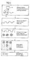
- FIG. 1shows a stage with the sensor and radiation source scanning a semiconductor device having an identification pattern with laser dot holes
- FIG. 2shows a side view of a laser dot hole, which is scanned with a laser and a sensor
- FIG. 3shows an embodiment of the apparatus using a position-sensitive device
- FIG. 4shows a top view of the stage being mounted on guide rails driven by motors
- FIG. 5shows a flowchart performed by the method of the present invention.
- the source of radiation 4which can be a laser, and a sensor 5 can be mounted on a stage 10 , as shown in FIG. 1.
- the stage 10can provide a scanning movement in both x- and y-direction at a constant height level above a semiconductor device 2 having a surface 2 a , on which an identification pattern 1 is structured by an arrangement of laser-engraved holes 3 .
- the semiconductor device 2can be a semiconductor wafer and the surface 2 a can be the wafer backside surface, and the identification pattern 1 is to be read out for performing an identification in, e.g., a sorter or another semiconductor processing tool.
- FIG. 2A side view of the scanning procedure is shown in FIG. 2. For illustrating the distance measurement, a cut is performed through the position of a hole 3 being engraved into the surface 2 a .
- Two scanning steps having a scanning pitch 24e.g., the horizontal distance between two laser beams, can be visualized in FIG. 2.
- the source of radiationi.e., the laser according to this embodiment, can concentrate its laser beam in a vertical direction directly onto the surface 2 a or hole 3 , respectively, below the laser 4 .
- the laser spot diameter 20can have a width of 10 nm, which is considerably smaller than the laser-engraved hole diameter 21 of 100 ⁇ m.
- a system of optical lenses 70 , 71can focus light emitted at a wavelength of 780 nm from a laser diode 4 onto a laser spot at the surface 2 a of a semiconductor wafer 2 being provided with holes 3 of an identification pattern 1 .
- the lightcan be emitted back through the optical lenses 70 , 71 onto a beam splitter 30 diffracting the beam onto a spot residing on a position-sensitive device 5 .
- the position-sensitive device 5can be connected to a measurer or means for determining the distance 6 of the surface 2 a to the sensor 5 .
- a measurer or means for determining the distance 6 of the surface 2 a to the sensor 5There are at least two possibilities, or embodiments, how the apparatus works measuring the distance:
- a distancecan be measured by an auto-focus measurement. If the laser spot on the surface 2 a runs out of focus due to a hole 3 or an elevation, the spot reflected through the optical lenses 70 , 71 and the beam splitter 30 onto the position-sensitive device 5 can become blurred or widened, and the corresponding widening shift of the spot, or the intensity or gradient, can be measured across the position-sensitive device (PSD-) array 5 .
- the measurer or means for determining the distance 6can be a processing unit receiving these array data, which can calculate the gradient or changed local intensity across the array into a defocus value, i.e., the amount of deviation current focus position from the corresponding surface position as being pointed to by the beam.
- a corresponding signalcan be sent to the control unit 8 , which can provide a movement of either one of the optical lenses 70 for establishing an optimum focus by the motor 7 , or can change the distance of the complete system, i.e., the optical lenses 70 , 71 , the beam splitter 30 and the position-sensitive device 5 from the surface 2 a .
- the measurer or means for determining the distance 6can determine the distance from the knowledge of the amount of defocus.
- the measurer or means for determining the distance 6can forward the distance data to the image processing unit 9 and the control unit 8 moving the optical system can forward positional data to the image processing unit 9 as well.
- the positional information and the distance informationcan be combined into a three-dimensional image of the surface structure 2 a in the identification pattern area.
- the distance valuecan be converted into a height value of the local surface area covered by the laser spot. If the distance of the position-sensitive device 5 from the surface 2 a is constant throughout the distance measurements, this procedure can be straightforward. If the distance has changed, particularly, in the case of an autofocus measurement, where the optical path length is held constant instead of the metric distance, the vertical height corrections by motor 7 or either the optical lens 70 or the complete optical system 70 , 71 , 30 , 4 , 5 are to be summed up by control unit 8 or the measurer or means for determining the distance 6 . The same is valid in the case of measuring the inclination if the optical system follows the surface profile by vertical height corrections. Here, the height changes are also to be summed up for adjacent measurements.
- the image processing unit 9can store the images in a database 50 and eventually can use a pattern recognition means or device 100 according to the method of the present invention for recovering a two-dimensional pattern of the wafer backside surface in order to identify the wafer.
- the systemcan have a measuring range in vertical height direction 23 of ⁇ 150 ⁇ m as compared to a depth 22 of holes 3 , which amounts to 100 ⁇ m if no dust or oxide layers are deposited inside holes 3 .
- the apparatuscan include guide rails 11 , 12 , which are each driven by motors 7 a , 7 b .
- the guide rails 12can be mounted on a frame 60 shown in the top view of FIG. 4.
- Guide rails 11can be mounted on these guide rails 11 fully disposable by motor 7 b , which can move the guide rails 11 along guide rails 11 by a metal band structured similarly as in floppy disk drives.
- Guide rails 11can be mounted on a motor stage 61 holding the second motor 7 a , which can have a similar structure as motor 7 b with metal bands, which by being unrolled provide a movement of the stage 10 , to which the metal band can be connected.
- Stage 10can also be mounted being freely disposable on guide rails 11 , thus providing a horizontal adjustment in a second direction 11 a , additionally to the first direction 12 a provided by the movement of the motor stage 61 along guide rails 12 .
- the method according to the present inventionis illustrated in FIG. 5.
- the apparatuscan start scanning the surface 2 a including holes 3 of the identification pattern 1 at a scan rate of 30 kHz.
- the identification pattern 1can include an area of 3.2 mm ⁇ 1.6 mm, such that the pitch or step width 24 amounts to 50 ⁇ m.
- its central opening areacan be, for example, 5 mm ⁇ 2 mm.
- a digitalized three-dimensional imagecan be obtained by the measurer or means for determining the distance 6 for obtaining height values, the control unit 8 for obtaining positional data, and the image processing unit 9 can combine these data.
- Applying a threshold level to the height valuesa binary one can be associated with the positional address values having a height value above this threshold level, and a binary zero with height values below this level.
- the three-dimensional imagecan be reduced to a two-dimensional image including areas associated with the one and with the zero value.
- the threshold valuemay be iteratively adjusted together with the following pattern recognition algorithm in order to obtain legible structures.
Landscapes
- Physics & Mathematics (AREA)
- General Physics & Mathematics (AREA)
- Engineering & Computer Science (AREA)
- Condensed Matter Physics & Semiconductors (AREA)
- Manufacturing & Machinery (AREA)
- Computer Hardware Design (AREA)
- Microelectronics & Electronic Packaging (AREA)
- Power Engineering (AREA)
- Length Measuring Devices By Optical Means (AREA)
Abstract
Description
- This application is a continuation of PCT Application No. PCT/EP02/10964, filed on Sep. 30, 2002, and titled “Semiconductor Device Identification Apparatus,” which claims priority from Euopean Patent Application No. EP 01123998.5, filed on Oct. 8, 2001, and titled “Semiconductor Device Identification Apparatus,” the entire contents of which are hereby incorporated by reference.[0001]
- The present invention relates to a semiconductor device identification apparatus for reading an identification pattern from the surface of a semiconductor device in a processing tool.[0002]
- In semiconductor device manufacturing, in particular, semiconductor wafers, it is often necessary to track single devices or lots through their sequence of processing steps. For this reason, each device is marked with a device identification number comprising, e.g., the lot name and the device number. In case of entering a processing tool, the device identification supplied on the device surface is read out in order to check, whether the correct device is currently being processed, and perhaps information is retrieved from a database, whether specific actions are to be taken for the current device.[0003]
- In the case of semiconductor wafers as an example, single wafer tracking is enabled by engraving the wafer identification onto the wafer backside surface in, e.g., the form of a dot matrix by use of a laser. A laser spot engraves a hole at a specified position in the matrix on the device surface, e.g. representing a binary “one”. If a matrix element position is free of an engraved laser dot, a binary “zero” is provided, then. Thus, the binary dot matrix can be read out and be interpreted in terms of an identification number.[0004]
- Alternatively, the matrix of dots directly corresponds to a structure providing a number or character when being recognized. Commonly, the device identification number is first read out by use of a CCD-camera, and second, identified by using a pattern recognition algorithm in an image processing unit.[0005]
- In the same way, it is also possible to structure elevations on the device surface, e.g., with the help of a laser depositing some material at predefined matrix positions. The read-out process and the recognition is then performed in the same way as described above.[0006]
- The approach using a CCD-camera has several disadvantages under productive circumstances. For example, the read-out rate of the engraved dot matrix can be too low originating from discoloration of the surface leading to ring-like structures on the surface layer of the semiconductor wafer. Such a ring running through a laser dot or hole can result in a non-detection of the corresponding matrix element, thereby issuing an error signal if the corresponding wrong wafer identification is currently not expected at the processing tool.[0007]
- Moreover, dust particles due to previous processing may have deposited inside the engraved holes, thereby additionally decreasing the color contrast, which is necessary for the optical CCD-camera approach. Also, deposited oxide layers lead to a reduction of the depth of the holes obliterating the sidewall contrast for the CCD-camera. In such cases, only concave surfaces indicate the existence of underlying laser-engraved holes.[0008]
- In order to circumvent these disadvantages, an apparatus using a laser emitting coherent light onto the laser dots or holes and a detector array receiving the light that is scattered at the concave sidewalls of laser holes being covered with an oxide layer is provided in DE 197 52 663 A1. There, a laser hole, or pattern, is recognized by an enhanced contrast due to the surface having plain, concave, or convex structure, thereby concentrating or diluting, respectively, the light scattered onto the array. Due to the enhanced contrast, a contrast-rich surface map of the wafer can be established by scanning the surface portion under investigation. The map of scattered light can then be evaluated into a potential map of the surface. Using an image processing unit with a pattern recognition algorithm, the wafer identification can then be performed.[0009]
- Unfortunately, this approach becomes particularly advantageous only in the case of the laser holes being obliterated by deposition of an oxide layer. If alternatively the laser inscription itself is not deteriorated, but rings of discoloration only impose changes of surface characteristics, the scattering approach becomes inefficient. Moreover, efforts have to be spent in order to calculate the potentials of the laser dots, and in case of dense matrices, it is questionable whether a unique potential solution can be expected. In the case of steep sidewalls of the laser holes, the contrast even reduces due to the lack of convex or concave surface elements.[0010]
- A semiconductor device identification apparatus can reduce erroneous reading of device identification patterns due to discolorations, while providing a high image pattern contrast for a large range of dot profiles. In particular, a semiconductor device identification apparatus for reading an identification pattern from the surface of a semiconductor device, in which identification pattern includes a matrix of holes or elevations formed in said surface, can include a source of radiation for irradiating the holes or elevations, a sensor for detecting the radiation being reflected from the surface and the holes or elevations, a means for determining the distance of the sensor to the semiconductor device surface, at least one motor for moving the sensor in at least one distance level above the surface, and a control unit for controlling the movement due to the at least one motor.[0011]
- The present invention can derive three-dimensional information of the device identification pattern area. For this purpose, for example, a measurer or a means for determining the distance of the sensor to the semiconductor device surface, or the holes or elevations respectively, can be provided. The distance measurements can be performed either by individually scanning the surface for retrieving local height levels of the surface, or the holes or elevations, or by performing multi-directional distance measurements from a predefined set of sensor positions. The first apparatus is more appropriate for sources of radiation working with light, while the latter aspect is convenient for acoustic radiation.[0012]
- Having obtained a distance map of the identification pattern surface, a three-dimensional surface map can be calculated, if the three-dimensional positions of the measuring sensor are known. The corresponding information can be provided by the control unit that controls the movement of the sensor performed by the motor, and the sensor, which provides distance raw data, which can be evaluated to real distance data. In case of a non-vertical direction of light being received by the sensor, directional information can also be needed. In this case, the control unit can maintain the movement of the direction of the optical path leading to the sensor.[0013]
- The present invention can work irrespective of colors. Thus, the problem of discolorations due to previous processes leading to erroneous wafer identification reading can be circumvented. The wavelength of the light used is not important for the present invention to work accurately. Although monochromatic light is preferred, multi-frequency radiation is generally possible.[0014]
- Also, the obliteration of the laser holes with dust or oxide layers on the one side or no contaminating particles on the other side do not put restrictions to the present invention. The present invention does not depend on the exact form of the surface profile. Only the distances are measured, and as long as height differences are immanent in significant amounts, the corresponding distance differences can be measured and the holes can be detected. Therefore, the present invention can offer a high variability and is not restricted to specific laser hole sidewall geometric forms. Rectangular steps as well as smooth concave or convex transitions can be detected by their distance to the sensor.[0015]
- In a further aspect, the radiation is considered to be a concentrated beam of light and the corresponding spot diameter is considered to be smaller than the diameter of the structure to be measured, i.e., the hole or elevation. In an exemplary configuration, the source of radiation is a laser. Using then a spot of this size, the profile of the laser hole can be scanned by subsequent measurements of the distance to the sensor, which, for example, can be moved across the surface in a horizontal direction. In a further aspect, the sensor can be considered to be a position-sensitive device (PSD), which can receive light through an optical system by a beam splitter. Such configurations for arbitrary distance measurements are commonly available and offer sufficient precision for performing distance measurements of pattern sizes provided for the present apparatus.[0016]
- In a further aspect, the image processing unit can include a pattern recognition means for identifying the identification pattern. There are two approaches possible: first, expected three-dimensional patterns, i.e., laser hole forms, as reference patterns can be compared with structures in the three-dimensional image, or second, the three-dimensional image can be reduced to a two-dimensional image by applying a threshold height value. Any height value above this threshold can be associated with a binary “one”, and those values below this threshold can be associated with a binary “zero”. The laser engravement procedure can structure into a two-dimensional pattern onto the surface.[0017]
- In a further aspect, the identification pattern can be considered to be a barcode using such a identification pattern, adjacent laser holes can be connected or at least provide a common structure, if taken together. The pattern recognition software can have a restricted number of structures possible in the dot matrix. The bars have the same length (with a few exceptions, for example, at the border) and a distinct choice of widths can be provided.[0018]
- As mentioned before, a further approach can use of acoustic waves for the radiation. Due to the limited velocity of these waves, run time differences can be measured due to which a distance measurement is possible. A three-dimensional profile of the identification pattern surface can be gained by locally emitting and receiving acoustic waves and the run time difference can provide the nearest distance of a surface element. This approach can use minimum size emitters and sensors.[0019]
- Another approach is to emit acoustic waves at three different positions above the identification pattern surface, and then recording the signal of reflected waves as a function of time. Recovering the surface profile from these reflected signals as a function of time involves some effort in computation, but which are well-known in the art.[0020]
- A method of identifying a semiconductor device using the apparatus of the present invention can include moving the source of radiation and the sensor to a first position above an identification pattern matrix of holes or elevations, irradiating a beam of radiation onto a first spot on the surface using the source of radiation, detecting the radiation which is reflected from the spot on the surface using the sensor, determining the first distance of the surface spot to the sensor using the means for determining the distance (measurer), repeating the steps described above for determining further distances of further surface spots to said sensor position, generating a three-dimensional image of surface heights from the distances as a function of position, and using a pattern recognition algorithm to identify said identification pattern matrix of holes or elevations.[0021]
- By this method, the surface can be scanned by distance measurements resulting in a three-dimensional image of surface height as a function of position, which can be input to an image processing unit for being applied to a pattern recognition algorithm for identifying the identification pattern of the semiconductor device.[0022]
- The invention will be better understood by reference to the following description of embodiments of the invention taken in conjunction with the accompanying drawings, wherein[0023]
- FIG. 1 shows a stage with the sensor and radiation source scanning a semiconductor device having an identification pattern with laser dot holes,[0024]
- FIG. 2 shows a side view of a laser dot hole, which is scanned with a laser and a sensor,[0025]
- FIG. 3 shows an embodiment of the apparatus using a position-sensitive device,[0026]
- FIG. 4 shows a top view of the stage being mounted on guide rails driven by motors, and[0027]
- FIG. 5 shows a flowchart performed by the method of the present invention.[0028]
- The source of[0029]
radiation 4, which can be a laser, and a sensor5 can be mounted on astage 10, as shown in FIG. 1. Thestage 10 can provide a scanning movement in both x- and y-direction at a constant height level above asemiconductor device 2 having asurface 2a, on which anidentification pattern 1 is structured by an arrangement of laser-engravedholes 3. Thesemiconductor device 2, according to this embodiment, can be a semiconductor wafer and thesurface 2acan be the wafer backside surface, and theidentification pattern 1 is to be read out for performing an identification in, e.g., a sorter or another semiconductor processing tool. - A side view of the scanning procedure is shown in FIG. 2. For illustrating the distance measurement, a cut is performed through the position of a[0030]
hole 3 being engraved into thesurface 2a. Two scanning steps having a scanningpitch 24, e.g., the horizontal distance between two laser beams, can be visualized in FIG. 2. The source of radiation, i.e., the laser according to this embodiment, can concentrate its laser beam in a vertical direction directly onto thesurface 2aorhole 3, respectively, below thelaser 4. In order to scan the hole profile, thelaser spot diameter 20 can have a width of 10 nm, which is considerably smaller than the laser-engravedhole diameter 21 of 100 μm. - In FIG. 3, the apparatus according to an embodiment of the present invention is shown in detail. A system of[0031]
optical lenses laser diode 4 onto a laser spot at thesurface 2aof asemiconductor wafer 2 being provided withholes 3 of anidentification pattern 1. The light can be emitted back through theoptical lenses beam splitter 30 diffracting the beam onto a spot residing on a position-sensitive device5. - The position-sensitive device[0032]5 can be connected to a measurer or means for determining the
distance 6 of thesurface 2ato the sensor5. There are at least two possibilities, or embodiments, how the apparatus works measuring the distance: - 1.) A distance can be measured by an auto-focus measurement. If the laser spot on the[0033]
surface 2aruns out of focus due to ahole 3 or an elevation, the spot reflected through theoptical lenses beam splitter 30 onto the position-sensitive device5 can become blurred or widened, and the corresponding widening shift of the spot, or the intensity or gradient, can be measured across the position-sensitive device (PSD-) array5. The measurer or means for determining thedistance 6 can be a processing unit receiving these array data, which can calculate the gradient or changed local intensity across the array into a defocus value, i.e., the amount of deviation current focus position from the corresponding surface position as being pointed to by the beam. A corresponding signal can be sent to the control unit8, which can provide a movement of either one of theoptical lenses 70 for establishing an optimum focus by the motor7, or can change the distance of the complete system, i.e., theoptical lenses beam splitter 30 and the position-sensitive device5 from thesurface 2a. In a vertical movement (horizontal in FIG. 3), the measurer or means for determining thedistance 6 can determine the distance from the knowledge of the amount of defocus. - 2.) Due to a[0034]
surface inclination 200 when entering ahole 3 on thesurface 2a, the reflected beam can be shifted, which can lead to a shift of the spot on the position-sensitive device5 (PSD). The corresponding shift in the array can then be detected by the measurer or means for determining thedistance 6 and can be converted into a distance value. - Using one of the two approaches, the measurer or means for determining the[0035]
distance 6 can forward the distance data to theimage processing unit 9 and the control unit8 moving the optical system can forward positional data to theimage processing unit 9 as well. The positional information and the distance information can be combined into a three-dimensional image of thesurface structure 2ain the identification pattern area. - For each x- and y-coordinate, the distance value can be converted into a height value of the local surface area covered by the laser spot. If the distance of the position-sensitive device[0036]5 from the
surface 2ais constant throughout the distance measurements, this procedure can be straightforward. If the distance has changed, particularly, in the case of an autofocus measurement, where the optical path length is held constant instead of the metric distance, the vertical height corrections by motor7 or either theoptical lens 70 or the completeoptical system distance 6. The same is valid in the case of measuring the inclination if the optical system follows the surface profile by vertical height corrections. Here, the height changes are also to be summed up for adjacent measurements. - The[0037]
image processing unit 9 can store the images in adatabase 50 and eventually can use a pattern recognition means ordevice 100 according to the method of the present invention for recovering a two-dimensional pattern of the wafer backside surface in order to identify the wafer. - The system can have a measuring range in[0038]
vertical height direction 23 of ±150 μm as compared to adepth 22 ofholes 3, which amounts to 100 μm if no dust or oxide layers are deposited inside holes3. - The technique of moving the[0039]
stage 10 across theidentification pattern 1 onsurface 2ais illustrated in FIG. 4. The apparatus can includeguide rails motors Guide rails 11 can be mounted on theseguide rails 11 fully disposable bymotor 7b, which can move the guide rails11 alongguide rails 11 by a metal band structured similarly as in floppy disk drives.Guide rails 11 can be mounted on amotor stage 61 holding thesecond motor 7a, which can have a similar structure asmotor 7bwith metal bands, which by being unrolled provide a movement of thestage 10, to which the metal band can be connected. - [0040]
Stage 10 can also be mounted being freely disposable onguide rails 11, thus providing a horizontal adjustment in asecond direction 11a, additionally to thefirst direction 12aprovided by the movement of themotor stage 61 along guide rails12. - The method according to the present invention is illustrated in FIG. 5. After providing the[0041]
semiconductor wafer 2 to the apparatus and aligning it, such that theidentification pattern 1 can take a defined position in front of the frame60 with the sensor and source of radiation having a default position, the apparatus can start scanning thesurface 2aincludingholes 3 of theidentification pattern 1 at a scan rate of 30 kHz. Theidentification pattern 1 can include an area of 3.2 mm×1.6 mm, such that the pitch orstep width 24 amounts to 50 μm. Using the frame60 of the present apparatus, its central opening area can be, for example, 5 mm×2 mm. - Using the apparatus according to the present invention, a digitalized three-dimensional image can be obtained by the measurer or means for determining the[0042]
distance 6 for obtaining height values, the control unit8 for obtaining positional data, and theimage processing unit 9 can combine these data. Applying a threshold level to the height values, a binary one can be associated with the positional address values having a height value above this threshold level, and a binary zero with height values below this level. Thereby, the three-dimensional image can be reduced to a two-dimensional image including areas associated with the one and with the zero value. The threshold value may be iteratively adjusted together with the following pattern recognition algorithm in order to obtain legible structures. - If the pattern recognition algorithm only expects binary-“one”-squares as reference patterns, these will eventually be recovered from the reduced two-dimensional image, and the corresponding matrix filling can be evaluated to provide the wafer identification number.[0043]
- While the invention has been described in detail and with reference to specific embodiments thereof, it will be apparent to one skilled in the art that various changes and modifications can be made therein without departing from the spirit and scope thereof. Accordingly, it is intended that the present invention covers the modifications and variations of this invention provided they come within the scope of the appended claims and their equivalents.[0044]
- [0045]1 identification pattern
- [0046]2 semiconductor device, wafer
- [0047]2adevice surface, wafer surface
- [0048]3 laser dot holes of identification pattern
- [0049]4 source of radiation, laser
- [0050]5 sensor, position-sensitive device
- [0051]6 means for determining the distance
- [0052]7 motor
- [0053]7amotor, x-direction
- [0054]7bmotor, y-direction
- [0055]8 control unit for motor
- [0056]9 image processing unit
- [0057]10 stage carrying sensor and source of radiation
- [0058]11 guide rail, x-direction
- [0059]11ax-direction
- [0060]12 guide rail in y-direction
- [0061]12ay-direction
- [0062]20 laser spot diameter
- [0063]21 hole diameter
- [0064]22 hole depth
- [0065]23 focus range, measuring range
- [0066]24 pitch, step width
- [0067]30 beam splitter
- [0068]50 database
- [0069]60 frame
- [0070]61 motor stage
- [0071]70 optical lens, movable for autofocus
- [0072]71 optical lens
- [0073]100 pattern recognition algorithm
- [0074]200 inclination
Claims (28)
Applications Claiming Priority (3)
| Application Number | Priority Date | Filing Date | Title |
|---|---|---|---|
| EPEP01123998.5 | 2001-10-08 | ||
| EP01123998AEP1300872A1 (en) | 2001-10-08 | 2001-10-08 | Semiconductor device identification apparatus |
| PCT/EP2002/010964WO2003032373A2 (en) | 2001-10-08 | 2002-09-30 | Semiconductor device identification apparatus |
Related Parent Applications (1)
| Application Number | Title | Priority Date | Filing Date |
|---|---|---|---|
| PCT/EP2002/010964ContinuationWO2003032373A2 (en) | 2001-10-08 | 2002-09-30 | Semiconductor device identification apparatus |
Publications (2)
| Publication Number | Publication Date |
|---|---|
| US20040238636A1true US20040238636A1 (en) | 2004-12-02 |
| US6866200B2 US6866200B2 (en) | 2005-03-15 |
Family
ID=8178888
Family Applications (1)
| Application Number | Title | Priority Date | Filing Date |
|---|---|---|---|
| US10/816,142Expired - Fee RelatedUS6866200B2 (en) | 2001-10-08 | 2004-04-02 | Semiconductor device identification apparatus |
Country Status (4)
| Country | Link |
|---|---|
| US (1) | US6866200B2 (en) |
| EP (1) | EP1300872A1 (en) |
| TW (1) | TW591689B (en) |
| WO (1) | WO2003032373A2 (en) |
Cited By (6)
| Publication number | Priority date | Publication date | Assignee | Title |
|---|---|---|---|---|
| CN103177235A (en)* | 2013-04-18 | 2013-06-26 | 河海大学常州校区 | Chinese-sensible code recognition device and Chinese-sensible code recognition method under complicated background |
| CN103994718A (en)* | 2014-05-27 | 2014-08-20 | 天津大学 | Tiny electronic element location recognition method based on microscope and computer vision |
| CN104424457A (en)* | 2013-08-20 | 2015-03-18 | 复旦大学 | Method for identifying two-dimensional code under the condition of nonlinear distortion |
| US20150345934A1 (en)* | 2012-12-27 | 2015-12-03 | Nova Measuring Instruments Ltd. | Optical method and system for critical dimensions and thickness characterization |
| US20150369595A1 (en)* | 2014-06-24 | 2015-12-24 | Byk-Gardner Gmbh | Multiple-stage method of investigating surfaces and corresponding apparatus |
| US20190064775A1 (en)* | 2017-07-20 | 2019-02-28 | Wuhan China Star Optoelectronics Semiconductor Display Technology Co., Ltd. | Complement method and system of the identification number used in the engraving machine |
Families Citing this family (9)
| Publication number | Priority date | Publication date | Assignee | Title |
|---|---|---|---|---|
| US7212330B2 (en)* | 2004-03-22 | 2007-05-01 | Angstrom, Inc. | Three-dimensional imaging system for pattern recognition |
| US7333218B2 (en)* | 2005-06-28 | 2008-02-19 | United Technologies Corporation | Systems and methods for determining the location and angular orientation of a hole with an obstructed opening residing on a surface of an article |
| US8006560B2 (en) | 2006-04-14 | 2011-08-30 | Toshiba Mitsubishi-Electric Industrial Systems Corporation | Laser ultrasonic property measurement apparatus |
| FR2905521A1 (en)* | 2006-08-31 | 2008-03-07 | Microcomposants De Haute Secur | METHOD OF MARKING A SEMICONDUCTOR PLATE FOR ITS IDENTIFICATION AND SEMICONDUCTOR PLATE MARKED THEREBY |
| JP4885762B2 (en)* | 2007-02-27 | 2012-02-29 | 株式会社ディスコ | Measuring device for workpiece held on chuck table and laser processing machine |
| US7953511B1 (en)* | 2007-09-21 | 2011-05-31 | National Semiconductor Corporation | System and method for reducing processing errors during wafer fabrication employing a 2D wafer scribe and monitoring system |
| TW201241399A (en)* | 2011-04-07 | 2012-10-16 | xi-ming Xu | Laser measurement device |
| CN103675897B (en)* | 2012-08-30 | 2017-10-27 | 中国石油化工股份有限公司 | A kind of earthquake diffracted wave method for separate imaging |
| US9400865B2 (en)* | 2014-06-13 | 2016-07-26 | Kla-Tencor Corp. | Extracting comprehensive design guidance for in-line process control tools and methods |
Citations (15)
| Publication number | Priority date | Publication date | Assignee | Title |
|---|---|---|---|---|
| US3636250A (en)* | 1964-02-26 | 1972-01-18 | Andrew V Haeff | Apparatus for scanning and reproducing a three-dimensional representation of an object |
| US4575719A (en)* | 1983-10-14 | 1986-03-11 | Avicom International, Inc. | Controlled access storage system |
| US4667087A (en)* | 1986-03-31 | 1987-05-19 | Max A. Quintana | Secure credit card |
| US4983842A (en)* | 1988-03-31 | 1991-01-08 | Tokyo Electron Limited | Image reading apparatus |
| US5155888A (en)* | 1991-05-22 | 1992-10-20 | Mactronix | Semiconductor wafer lifter |
| US5197650A (en)* | 1990-09-18 | 1993-03-30 | Sharp Kabushiki Kaisha | Die bonding apparatus |
| US5287414A (en)* | 1991-06-21 | 1994-02-15 | Esselte Pendaflex Corporation | Coded file locator system |
| US5559446A (en)* | 1993-07-19 | 1996-09-24 | Tokyo Electron Kabushiki Kaisha | Probing method and device |
| US5567927A (en)* | 1994-07-25 | 1996-10-22 | Texas Instruments Incorporated | Apparatus for semiconductor wafer identification |
| US5883374A (en)* | 1997-03-27 | 1999-03-16 | Advanced Micro Devices, Inc. | Scanning system for identifying wafers in semiconductor process tool chambers |
| US5942763A (en)* | 1997-04-11 | 1999-08-24 | Mitsubishi Denki Kabushiki Kaisha | Apparatus and method for identifying an identification mark of a wafer |
| US6075373A (en)* | 1996-05-31 | 2000-06-13 | Tokyo Electron Limited | Inspection device for inspecting a semiconductor wafer |
| US6168296B1 (en)* | 1997-06-23 | 2001-01-02 | Ccs Co., Ltd. | Lighting unit for reading marks |
| US6215551B1 (en)* | 1994-12-08 | 2001-04-10 | Kla-Tencor Corporation | Scanning system for inspecting anomalies on surfaces |
| US6617172B2 (en)* | 2000-12-15 | 2003-09-09 | Hitachi, Ltd. | Semiconductor device having identification number, manufacturing method thereof and electronic device |
Family Cites Families (11)
| Publication number | Priority date | Publication date | Assignee | Title |
|---|---|---|---|---|
| JPS61236117A (en)* | 1985-04-12 | 1986-10-21 | Hitachi Ltd | Pattern position detecting method |
| JPS63108736A (en)* | 1986-10-27 | 1988-05-13 | Mitsubishi Electric Corp | Wafer prober device |
| WO1991018313A1 (en)* | 1990-05-21 | 1991-11-28 | Interactive Video Systems, Inc. | Projected image focus system and method of use |
| JPH05203583A (en)* | 1992-01-23 | 1993-08-10 | Sony Corp | Visual inspection method |
| JPH06112300A (en) | 1992-09-25 | 1994-04-22 | Matsushita Electron Corp | Device for reading semiconductor wafer id |
| US6321601B1 (en)* | 1996-08-06 | 2001-11-27 | Brown University Research Foundation | Optical method for the characterization of laterally-patterned samples in integrated circuits |
| FR2751769B1 (en) | 1996-07-29 | 1998-10-09 | Recif Sa | METHOD AND APPARATUS FOR IDENTIFYING CHARACTERS FORMED ON A PLURALITY OF SILICON WAFERS |
| JPH10185530A (en) | 1996-08-23 | 1998-07-14 | Asahi Optical Co Ltd | Pattern reader |
| JPH10255026A (en) | 1997-03-11 | 1998-09-25 | Asahi Optical Co Ltd | Pattern reader |
| JPH11145017A (en)* | 1997-11-04 | 1999-05-28 | Oki Electric Ind Co Ltd | Wafer writing method and wafer reading method |
| JP2001101337A (en)* | 1999-07-26 | 2001-04-13 | Komatsu Ltd | Dot mark reading device and reading method |
- 2001
- 2001-10-08EPEP01123998Apatent/EP1300872A1/ennot_activeWithdrawn
- 2002
- 2002-09-30WOPCT/EP2002/010964patent/WO2003032373A2/ennot_activeApplication Discontinuation
- 2002-10-07TWTW091123090Apatent/TW591689B/ennot_activeIP Right Cessation
- 2004
- 2004-04-02USUS10/816,142patent/US6866200B2/ennot_activeExpired - Fee Related
Patent Citations (16)
| Publication number | Priority date | Publication date | Assignee | Title |
|---|---|---|---|---|
| US3636250A (en)* | 1964-02-26 | 1972-01-18 | Andrew V Haeff | Apparatus for scanning and reproducing a three-dimensional representation of an object |
| US4575719A (en)* | 1983-10-14 | 1986-03-11 | Avicom International, Inc. | Controlled access storage system |
| US4667087A (en)* | 1986-03-31 | 1987-05-19 | Max A. Quintana | Secure credit card |
| US4983842A (en)* | 1988-03-31 | 1991-01-08 | Tokyo Electron Limited | Image reading apparatus |
| US5197650A (en)* | 1990-09-18 | 1993-03-30 | Sharp Kabushiki Kaisha | Die bonding apparatus |
| US5155888A (en)* | 1991-05-22 | 1992-10-20 | Mactronix | Semiconductor wafer lifter |
| US5287414A (en)* | 1991-06-21 | 1994-02-15 | Esselte Pendaflex Corporation | Coded file locator system |
| US5982183A (en)* | 1993-07-19 | 1999-11-09 | Tokyo Electron Limited | Probing method and device with contact film wiper feature |
| US5559446A (en)* | 1993-07-19 | 1996-09-24 | Tokyo Electron Kabushiki Kaisha | Probing method and device |
| US5567927A (en)* | 1994-07-25 | 1996-10-22 | Texas Instruments Incorporated | Apparatus for semiconductor wafer identification |
| US6215551B1 (en)* | 1994-12-08 | 2001-04-10 | Kla-Tencor Corporation | Scanning system for inspecting anomalies on surfaces |
| US6075373A (en)* | 1996-05-31 | 2000-06-13 | Tokyo Electron Limited | Inspection device for inspecting a semiconductor wafer |
| US5883374A (en)* | 1997-03-27 | 1999-03-16 | Advanced Micro Devices, Inc. | Scanning system for identifying wafers in semiconductor process tool chambers |
| US5942763A (en)* | 1997-04-11 | 1999-08-24 | Mitsubishi Denki Kabushiki Kaisha | Apparatus and method for identifying an identification mark of a wafer |
| US6168296B1 (en)* | 1997-06-23 | 2001-01-02 | Ccs Co., Ltd. | Lighting unit for reading marks |
| US6617172B2 (en)* | 2000-12-15 | 2003-09-09 | Hitachi, Ltd. | Semiconductor device having identification number, manufacturing method thereof and electronic device |
Cited By (10)
| Publication number | Priority date | Publication date | Assignee | Title |
|---|---|---|---|---|
| US20150345934A1 (en)* | 2012-12-27 | 2015-12-03 | Nova Measuring Instruments Ltd. | Optical method and system for critical dimensions and thickness characterization |
| US10054423B2 (en)* | 2012-12-27 | 2018-08-21 | Nova Measuring Instruments Ltd. | Optical method and system for critical dimensions and thickness characterization |
| CN103177235A (en)* | 2013-04-18 | 2013-06-26 | 河海大学常州校区 | Chinese-sensible code recognition device and Chinese-sensible code recognition method under complicated background |
| CN104424457A (en)* | 2013-08-20 | 2015-03-18 | 复旦大学 | Method for identifying two-dimensional code under the condition of nonlinear distortion |
| CN103994718A (en)* | 2014-05-27 | 2014-08-20 | 天津大学 | Tiny electronic element location recognition method based on microscope and computer vision |
| US20150369595A1 (en)* | 2014-06-24 | 2015-12-24 | Byk-Gardner Gmbh | Multiple-stage method of investigating surfaces and corresponding apparatus |
| CN105277558A (en)* | 2014-06-24 | 2016-01-27 | 毕克-加特纳有限责任公司 | Multiple-stage method of investigating surfaces and corresponding apparatus |
| US11300406B2 (en)* | 2014-06-24 | 2022-04-12 | Byk-Gardner Gmbh | Multiple-stage method of investigating surfaces and corresponding apparatus |
| US20190064775A1 (en)* | 2017-07-20 | 2019-02-28 | Wuhan China Star Optoelectronics Semiconductor Display Technology Co., Ltd. | Complement method and system of the identification number used in the engraving machine |
| US10838397B2 (en)* | 2017-07-20 | 2020-11-17 | Wuhan China Star Optoelectronics Semiconductor Display Technology Co., Ltd. | Complement method and system of the identification number used in the engraving machine |
Also Published As
| Publication number | Publication date |
|---|---|
| WO2003032373A2 (en) | 2003-04-17 |
| US6866200B2 (en) | 2005-03-15 |
| EP1300872A1 (en) | 2003-04-09 |
| WO2003032373A3 (en) | 2003-12-18 |
| TW591689B (en) | 2004-06-11 |
Similar Documents
| Publication | Publication Date | Title |
|---|---|---|
| US6866200B2 (en) | Semiconductor device identification apparatus | |
| US4860374A (en) | Apparatus for detecting position of reference pattern | |
| JP2641829B2 (en) | Bending angle detection device in bending machine | |
| EP0114517A1 (en) | Mark position detecting method and apparatus | |
| US12172430B2 (en) | Substrate positioning for deposition machine | |
| JP5508734B2 (en) | Pattern drawing apparatus and pattern drawing method | |
| US6721058B2 (en) | Apparatus for and method of measuring thickness of materials using the focal length of a lensed fiber | |
| JP3391470B2 (en) | Projection exposure apparatus and projection exposure method | |
| JP2003109985A (en) | Wafer bump inspection method and wafer bump inspection device | |
| JP3640012B2 (en) | Method for measuring level of mask or wafer in exposure apparatus and measurement control apparatus | |
| US6812479B2 (en) | Sample positioning method for surface optical diagnostics using video imaging | |
| JPH11135390A (en) | Wafer on which id is printed, manufacture of semiconductor device and manufacture equipment therefor | |
| JP7285433B2 (en) | LASER PROCESSING APPARATUS AND LASER PROCESSING METHOD | |
| US20080151246A1 (en) | Alignment routine for optically based tools | |
| JPS59164910A (en) | distance measuring device | |
| JPH09106945A (en) | Particle beam alignment method and irradiation method and apparatus using the same | |
| JP2001059716A (en) | Device for measuring inclination angle of inclined flat surface and laser marker and mark reading device provided with the same | |
| JPS61255020A (en) | Mark detection method in charged beam exposure equipment | |
| JPH0346220A (en) | Focus setting method for electron beam lithography and exposure device | |
| JP3040881B2 (en) | Light beam diameter measuring device | |
| JP2986130B2 (en) | Mark detection processing method | |
| JP2828320B2 (en) | Electron beam length measurement method | |
| JP2946336B2 (en) | Sample surface height detector | |
| JPS63271618A (en) | Aligning mark and aligning method | |
| JPH0518780U (en) | Laser beam positioning device |
Legal Events
| Date | Code | Title | Description |
|---|---|---|---|
| AS | Assignment | Owner name:INFINEON TECHNOLOGIES SC300 GMBH & CO. KG, GERMANY Free format text:ASSIGNMENT OF ASSIGNORS INTEREST;ASSIGNORS:MARX, ECKHARD;PEITER, MARTIN;REEL/FRAME:015649/0074 Effective date:20040720 | |
| FEPP | Fee payment procedure | Free format text:PAYOR NUMBER ASSIGNED (ORIGINAL EVENT CODE: ASPN); ENTITY STATUS OF PATENT OWNER: LARGE ENTITY | |
| CC | Certificate of correction | ||
| FPAY | Fee payment | Year of fee payment:4 | |
| AS | Assignment | Owner name:QIMONDA AG, GERMANY Free format text:ASSIGNMENT OF ASSIGNORS INTEREST;ASSIGNOR:INFINEON TECHNOLOGIES SC300 GMBH & CO. KG;REEL/FRAME:023854/0001 Effective date:20060425 | |
| FPAY | Fee payment | Year of fee payment:8 | |
| AS | Assignment | Owner name:INFINEON TECHNOLOGIES AG, GERMANY Free format text:ASSIGNMENT OF ASSIGNORS INTEREST;ASSIGNOR:QIMONDA AG;REEL/FRAME:035623/0001 Effective date:20141009 | |
| AS | Assignment | Owner name:POLARIS INNOVATIONS LIMITED, IRELAND Free format text:ASSIGNMENT OF ASSIGNORS INTEREST;ASSIGNOR:INFINEON TECHNOLOGIES AG;REEL/FRAME:036615/0885 Effective date:20150708 | |
| REMI | Maintenance fee reminder mailed | ||
| LAPS | Lapse for failure to pay maintenance fees | ||
| STCH | Information on status: patent discontinuation | Free format text:PATENT EXPIRED DUE TO NONPAYMENT OF MAINTENANCE FEES UNDER 37 CFR 1.362 | |
| FP | Lapsed due to failure to pay maintenance fee | Effective date:20170315 |