US20040235216A1 - Multi-trench region for accumulation of photo-generated charge in a CMOS imager - Google Patents
Multi-trench region for accumulation of photo-generated charge in a CMOS imagerDownload PDFInfo
- Publication number
- US20040235216A1 US20040235216A1US10/871,018US87101804AUS2004235216A1US 20040235216 A1US20040235216 A1US 20040235216A1US 87101804 AUS87101804 AUS 87101804AUS 2004235216 A1US2004235216 A1US 2004235216A1
- Authority
- US
- United States
- Prior art keywords
- doped
- transistor
- photosensor
- charge
- pixel
- Prior art date
- Legal status (The legal status is an assumption and is not a legal conclusion. Google has not performed a legal analysis and makes no representation as to the accuracy of the status listed.)
- Granted
Links
- 238000009825accumulationMethods0.000titledescription5
- 238000000034methodMethods0.000claimsabstractdescription39
- 239000000758substrateSubstances0.000claimsabstractdescription37
- 230000008569processEffects0.000claimsabstractdescription23
- 239000004065semiconductorSubstances0.000claimsdescription24
- 238000005468ion implantationMethods0.000claimsdescription6
- 238000001020plasma etchingMethods0.000claimsdescription5
- 238000009792diffusion processMethods0.000description31
- VYPSYNLAJGMNEJ-UHFFFAOYSA-NSilicium dioxideChemical compoundO=[Si]=OVYPSYNLAJGMNEJ-UHFFFAOYSA-N0.000description18
- 239000003990capacitorSubstances0.000description11
- 239000000463materialSubstances0.000description11
- 239000000377silicon dioxideSubstances0.000description9
- 235000012239silicon dioxideNutrition0.000description9
- XUIMIQQOPSSXEZ-UHFFFAOYSA-NSiliconChemical compound[Si]XUIMIQQOPSSXEZ-UHFFFAOYSA-N0.000description8
- 238000003384imaging methodMethods0.000description8
- 229910052710siliconInorganic materials0.000description8
- 239000010703siliconSubstances0.000description8
- 238000005516engineering processMethods0.000description7
- 229910052581Si3N4Inorganic materials0.000description6
- 238000005530etchingMethods0.000description6
- HQVNEWCFYHHQES-UHFFFAOYSA-Nsilicon nitrideChemical compoundN12[Si]34N5[Si]62N3[Si]51N64HQVNEWCFYHHQES-UHFFFAOYSA-N0.000description6
- 238000003491arrayMethods0.000description5
- 239000007943implantSubstances0.000description5
- 150000002500ionsChemical class0.000description5
- 229910052751metalInorganic materials0.000description5
- 239000002184metalSubstances0.000description5
- 229910021420polycrystalline siliconInorganic materials0.000description5
- 229920005591polysiliconPolymers0.000description5
- WFKWXMTUELFFGS-UHFFFAOYSA-NtungstenChemical compound[W]WFKWXMTUELFFGS-UHFFFAOYSA-N0.000description5
- 229910052721tungstenInorganic materials0.000description5
- 239000010937tungstenSubstances0.000description5
- 239000004020conductorSubstances0.000description4
- 238000010586diagramMethods0.000description4
- 239000012212insulatorSubstances0.000description4
- 230000010354integrationEffects0.000description4
- 238000004519manufacturing processMethods0.000description4
- 230000003647oxidationEffects0.000description4
- 238000007254oxidation reactionMethods0.000description4
- 230000015572biosynthetic processEffects0.000description3
- 230000006870functionEffects0.000description3
- 238000003860storageMethods0.000description3
- JBRZTFJDHDCESZ-UHFFFAOYSA-NAsGaChemical compound[As]#[Ga]JBRZTFJDHDCESZ-UHFFFAOYSA-N0.000description2
- 229910001218Gallium arsenideInorganic materials0.000description2
- 229910000577Silicon-germaniumInorganic materials0.000description2
- 230000003321amplificationEffects0.000description2
- 239000005380borophosphosilicate glassSubstances0.000description2
- 238000006243chemical reactionMethods0.000description2
- 238000005229chemical vapour depositionMethods0.000description2
- 230000003750conditioning effectEffects0.000description2
- 238000013144data compressionMethods0.000description2
- 238000000151depositionMethods0.000description2
- 238000001514detection methodMethods0.000description2
- 230000005670electromagnetic radiationEffects0.000description2
- 230000005669field effectEffects0.000description2
- 238000001465metallisationMethods0.000description2
- 238000003199nucleic acid amplification methodMethods0.000description2
- 230000004044responseEffects0.000description2
- 238000005070samplingMethods0.000description2
- 229910052594sapphireInorganic materials0.000description2
- 239000010980sapphireSubstances0.000description2
- 230000006641stabilisationEffects0.000description2
- 238000011105stabilizationMethods0.000description2
- NXHILIPIEUBEPD-UHFFFAOYSA-Htungsten hexafluorideChemical compoundF[W](F)(F)(F)(F)FNXHILIPIEUBEPD-UHFFFAOYSA-H0.000description2
- RYGMFSIKBFXOCR-UHFFFAOYSA-NCopperChemical compound[Cu]RYGMFSIKBFXOCR-UHFFFAOYSA-N0.000description1
- 241000819554MendisSpecies0.000description1
- LEVVHYCKPQWKOP-UHFFFAOYSA-N[Si].[Ge]Chemical compound[Si].[Ge]LEVVHYCKPQWKOP-UHFFFAOYSA-N0.000description1
- 229910052782aluminiumInorganic materials0.000description1
- XAGFODPZIPBFFR-UHFFFAOYSA-NaluminiumChemical compound[Al]XAGFODPZIPBFFR-UHFFFAOYSA-N0.000description1
- 230000009286beneficial effectEffects0.000description1
- 229910052802copperInorganic materials0.000description1
- 239000010949copperSubstances0.000description1
- 230000002596correlated effectEffects0.000description1
- 230000000779depleting effectEffects0.000description1
- 230000008021depositionEffects0.000description1
- 230000001066destructive effectEffects0.000description1
- 230000008020evaporationEffects0.000description1
- 238000001704evaporationMethods0.000description1
- 238000011049fillingMethods0.000description1
- 229910052732germaniumInorganic materials0.000description1
- GNPVGFCGXDBREM-UHFFFAOYSA-Ngermanium atomChemical compound[Ge]GNPVGFCGXDBREM-UHFFFAOYSA-N0.000description1
- 238000002513implantationMethods0.000description1
- AMGQUBHHOARCQH-UHFFFAOYSA-Nindium;oxotinChemical compound[In].[Sn]=OAMGQUBHHOARCQH-UHFFFAOYSA-N0.000description1
- 238000002347injectionMethods0.000description1
- 239000007924injectionSubstances0.000description1
- 238000002955isolationMethods0.000description1
- 150000002736metal compoundsChemical class0.000description1
- 238000002161passivationMethods0.000description1
- 230000002093peripheral effectEffects0.000description1
- 238000003672processing methodMethods0.000description1
- 230000005855radiationEffects0.000description1
- 230000009467reductionEffects0.000description1
- 229910021332silicideInorganic materials0.000description1
- FVBUAEGBCNSCDD-UHFFFAOYSA-Nsilicide(4-)Chemical compound[Si-4]FVBUAEGBCNSCDD-UHFFFAOYSA-N0.000description1
- 239000002210silicon-based materialSubstances0.000description1
- 239000007787solidSubstances0.000description1
- 125000006850spacer groupChemical group0.000description1
- 238000004544sputter depositionMethods0.000description1
- XOLBLPGZBRYERU-UHFFFAOYSA-Ntin dioxideChemical compoundO=[Sn]=OXOLBLPGZBRYERU-UHFFFAOYSA-N0.000description1
- 229910001887tin oxideInorganic materials0.000description1
Images


Classifications
- H—ELECTRICITY
- H10—SEMICONDUCTOR DEVICES; ELECTRIC SOLID-STATE DEVICES NOT OTHERWISE PROVIDED FOR
- H10F—INORGANIC SEMICONDUCTOR DEVICES SENSITIVE TO INFRARED RADIATION, LIGHT, ELECTROMAGNETIC RADIATION OF SHORTER WAVELENGTH OR CORPUSCULAR RADIATION
- H10F39/00—Integrated devices, or assemblies of multiple devices, comprising at least one element covered by group H10F30/00, e.g. radiation detectors comprising photodiode arrays
- H10F39/10—Integrated devices
- H10F39/12—Image sensors
- H10F39/18—Complementary metal-oxide-semiconductor [CMOS] image sensors; Photodiode array image sensors
- H—ELECTRICITY
- H10—SEMICONDUCTOR DEVICES; ELECTRIC SOLID-STATE DEVICES NOT OTHERWISE PROVIDED FOR
- H10F—INORGANIC SEMICONDUCTOR DEVICES SENSITIVE TO INFRARED RADIATION, LIGHT, ELECTROMAGNETIC RADIATION OF SHORTER WAVELENGTH OR CORPUSCULAR RADIATION
- H10F30/00—Individual radiation-sensitive semiconductor devices in which radiation controls the flow of current through the devices, e.g. photodetectors
- H10F30/20—Individual radiation-sensitive semiconductor devices in which radiation controls the flow of current through the devices, e.g. photodetectors the devices having potential barriers, e.g. phototransistors
- H10F30/21—Individual radiation-sensitive semiconductor devices in which radiation controls the flow of current through the devices, e.g. photodetectors the devices having potential barriers, e.g. phototransistors the devices being sensitive to infrared, visible or ultraviolet radiation
- H10F30/22—Individual radiation-sensitive semiconductor devices in which radiation controls the flow of current through the devices, e.g. photodetectors the devices having potential barriers, e.g. phototransistors the devices being sensitive to infrared, visible or ultraviolet radiation the devices having only one potential barrier, e.g. photodiodes
- H10F30/221—Individual radiation-sensitive semiconductor devices in which radiation controls the flow of current through the devices, e.g. photodetectors the devices having potential barriers, e.g. phototransistors the devices being sensitive to infrared, visible or ultraviolet radiation the devices having only one potential barrier, e.g. photodiodes the potential barrier being a PN homojunction
- H—ELECTRICITY
- H10—SEMICONDUCTOR DEVICES; ELECTRIC SOLID-STATE DEVICES NOT OTHERWISE PROVIDED FOR
- H10F—INORGANIC SEMICONDUCTOR DEVICES SENSITIVE TO INFRARED RADIATION, LIGHT, ELECTROMAGNETIC RADIATION OF SHORTER WAVELENGTH OR CORPUSCULAR RADIATION
- H10F39/00—Integrated devices, or assemblies of multiple devices, comprising at least one element covered by group H10F30/00, e.g. radiation detectors comprising photodiode arrays
- H10F39/011—Manufacture or treatment of image sensors covered by group H10F39/12
- H10F39/014—Manufacture or treatment of image sensors covered by group H10F39/12 of CMOS image sensors
- H—ELECTRICITY
- H10—SEMICONDUCTOR DEVICES; ELECTRIC SOLID-STATE DEVICES NOT OTHERWISE PROVIDED FOR
- H10F—INORGANIC SEMICONDUCTOR DEVICES SENSITIVE TO INFRARED RADIATION, LIGHT, ELECTROMAGNETIC RADIATION OF SHORTER WAVELENGTH OR CORPUSCULAR RADIATION
- H10F39/00—Integrated devices, or assemblies of multiple devices, comprising at least one element covered by group H10F30/00, e.g. radiation detectors comprising photodiode arrays
- H10F39/011—Manufacture or treatment of image sensors covered by group H10F39/12
- H10F39/026—Wafer-level processing
- H—ELECTRICITY
- H10—SEMICONDUCTOR DEVICES; ELECTRIC SOLID-STATE DEVICES NOT OTHERWISE PROVIDED FOR
- H10F—INORGANIC SEMICONDUCTOR DEVICES SENSITIVE TO INFRARED RADIATION, LIGHT, ELECTROMAGNETIC RADIATION OF SHORTER WAVELENGTH OR CORPUSCULAR RADIATION
- H10F39/00—Integrated devices, or assemblies of multiple devices, comprising at least one element covered by group H10F30/00, e.g. radiation detectors comprising photodiode arrays
- H10F39/80—Constructional details of image sensors
- H10F39/807—Pixel isolation structures
- H—ELECTRICITY
- H10—SEMICONDUCTOR DEVICES; ELECTRIC SOLID-STATE DEVICES NOT OTHERWISE PROVIDED FOR
- H10F—INORGANIC SEMICONDUCTOR DEVICES SENSITIVE TO INFRARED RADIATION, LIGHT, ELECTROMAGNETIC RADIATION OF SHORTER WAVELENGTH OR CORPUSCULAR RADIATION
- H10F77/00—Constructional details of devices covered by this subclass
- H10F77/10—Semiconductor bodies
- H10F77/14—Shape of semiconductor bodies; Shapes, relative sizes or dispositions of semiconductor regions within semiconductor bodies
- H10F77/148—Shapes of potential barriers
- H—ELECTRICITY
- H10—SEMICONDUCTOR DEVICES; ELECTRIC SOLID-STATE DEVICES NOT OTHERWISE PROVIDED FOR
- H10F—INORGANIC SEMICONDUCTOR DEVICES SENSITIVE TO INFRARED RADIATION, LIGHT, ELECTROMAGNETIC RADIATION OF SHORTER WAVELENGTH OR CORPUSCULAR RADIATION
- H10F77/00—Constructional details of devices covered by this subclass
- H10F77/10—Semiconductor bodies
- H10F77/14—Shape of semiconductor bodies; Shapes, relative sizes or dispositions of semiconductor regions within semiconductor bodies
- H10F77/147—Shapes of bodies
- Y—GENERAL TAGGING OF NEW TECHNOLOGICAL DEVELOPMENTS; GENERAL TAGGING OF CROSS-SECTIONAL TECHNOLOGIES SPANNING OVER SEVERAL SECTIONS OF THE IPC; TECHNICAL SUBJECTS COVERED BY FORMER USPC CROSS-REFERENCE ART COLLECTIONS [XRACs] AND DIGESTS
- Y02—TECHNOLOGIES OR APPLICATIONS FOR MITIGATION OR ADAPTATION AGAINST CLIMATE CHANGE
- Y02E—REDUCTION OF GREENHOUSE GAS [GHG] EMISSIONS, RELATED TO ENERGY GENERATION, TRANSMISSION OR DISTRIBUTION
- Y02E10/00—Energy generation through renewable energy sources
- Y02E10/50—Photovoltaic [PV] energy
Definitions
- the inventionrelates generally to improved semiconductor imaging devices and in particular to a silicon imaging device which can be fabricated using a standard CMOS process. Particularly, the invention relates to a multi-trench region for accumulation of photo-generated charge in a CMOS imager.
- CCDscharge coupled devices
- photodiode arrayscharge injection devices
- hybrid focal plane arraysCCDs
- CCDsare often employed for image acquisition and enjoy a number of advantages which makes it the incumbent technology, particularly for small size imaging applications.
- CCDsare also capable of large formats with small pixel size and they employ low noise charge domain processing techniques.
- CCD imagersalso suffer from a number of disadvantages. For example, they are susceptible to radiation damage, they exhibit destructive read out over time, they require good light shielding to avoid image smear and they have a high power dissipation for large arrays.
- CCD arraysare difficult to integrate with CMOS processing in part due to a different processing technology and to their high capacitances, complicating the integration of on-chip drive and signal processing electronics with the CCD array. While there has been some attempts to integrate on-chip signal processing with the CCD array, these attempts have not been entirely successful. CCDs also must transfer an image by line charge transfers from pixel to pixel, requiring that the entire array be read out into a memory before individual pixels or groups of pixels can be accessed and processed. This takes time. CCDs may also suffer from incomplete charge transfer from pixel to pixel during charge transfer which also results in image smear.
- CMOS imagersBecause of the inherent limitations in CCD technology, there is an interest in CMOS imagers for possible use as low cost imaging devices.
- a fully compatible CMOS sensor technology enabling a higher level of integration of an image array with associated processing circuitswould be beneficial to many digital applications such as, for example, in cameras, scanners, machine vision systems, vehicle navigation systems, video telephones, computer input devices, surveillance systems, auto focus systems, star trackers, motion detection systems, image stabilization systems and data compression systems for high-definition television.
- CMOS imagershave a low voltage operation and low power consumption; CMOS imagers are compatible with integrated on-chip electronics (control logic and timing, image processing, and signal conditioning such as A/D conversion); CMOS imagers allow random access to the image data; and CMOS imagers have lower fabrication costs as compared with the conventional CCD since standard CMOS processing techniques can be used. Additionally, low power consumption is achieved for CMOS imagers because only one row of pixels at a time needs to be active during the readout and there is no charge transfer (and associated switching) from pixel to pixel during image acquisition. On-chip integration of electronics is particularly advantageous because of the potential to perform many signal conditioning functions in the digital domain (versus analog signal processing) as well as to achieve a reduction in system size and cost.
- a CMOS imager circuitincludes a focal plane array of pixel cells, each one of the cells including either a photogate, a photodiode, or a photoconductor overlying a substrate for accumulating photo-generated charge in the underlying portion of the substrate.
- a readout circuitis connected to each pixel cell and includes at least an output field effect transistor formed in the substrate and a charge transfer section formed on the substrate adjacent the photogate, photodiode, or the photoconductor having a sensing node, typically a floating diffusion node, connected to the gate of an output transistor.
- the imagermay include at least one electronic device such as a transistor for transferring charge from the underlying portion of the substrate to the floating diffusion node and one device, also typically a transistor, for resetting the node to a predetermined charge level prior to charge transference.
- the active elements of a pixel cellperform the necessary functions of: (1) photon to charge conversion; (2) accumulation of image charge; (3) transfer of charge to the floating diffusion node accompanied by charge amplification; (4) resetting the floating diffusion node to a known state before the transfer of charge to it; (5) selection of a pixel for readout; and (6) output and amplification of a signal representing pixel charge.
- Photo chargemay be amplified when it moves from the initial charge accumulation region to the floating diffusion node.
- the charge at the floating diffusion nodeis typically converted to a pixel output voltage by a source follower output transistor.
- the photosensitive element of a CMOS imager pixelis typically either a depleted p-n junction photodiode or a field induced depletion region beneath a photogate or a photoconductor.
- image lagcan be eliminated by completely depleting the photodiode upon readout.
- CMOS imagers of the type discussed aboveare generally known as discussed, for example, in Nixon et al., “256 ⁇ 256 CMOS Active Pixel Sensor Camera-on-a-Chip,” IEEE Journal of Solid-State Circuits, Vol. 31(12) pp. 2046-2050, 1996; Mendis et al, “CMOS Active Pixel Image Sensors,” IEEE Transactions on Electron Devices, Vol. 41(3) pp. 452-453, 1994 as well as U.S. Pat. No. 5,708,263 and U.S. Pat. No. 5,471,515, which are herein incorporated by reference.
- CMOS imaging circuitincludes a photogate for accumulating photo-generated charge in an underlying portion of the substrate.
- CMOS imagermay include a photodiode or other image to charge converting device, in lieu of a photogate, as the initial accumulator for photo-generated charge.
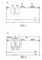
- FIG. 1shows a simplified circuit for a pixel of an exemplary CMOS imager using a photogate and having a pixel photodetector circuit 14 and a readout circuit 60 .
- FIG. 1shows the circuitry for operation of a single pixel, that in practical use there will be an M ⁇ N array of pixels arranged in rows and columns with the pixels of the array accessed using row and column select circuitry, as described in more detail below.
- the photodetector circuit 14is shown in part as a cross-sectional view of a semiconductor substrate 16 typically of a p-type silicon, having a surface well of p-type material 20 .
- An optional layer 18 of p-type materialmay be used if desired, but is not required.
- Substrate 16may be formed of, for example, Si, SiGe, Ge, and GaAs.
- the entire substrate 16is p-type doped silicon substrate and may contain a surface p-well 20 (with layer 18 omitted), but many other options are possible, such as, for example p on p ⁇ substrates, p on p+ substrates, p-wells in n-type substrates or the like.
- wafer or substrate used in the descriptionincludes any semiconductor-based structure having an exposed surface in which to form the circuit structure used in the invention.
- Wafer and substrateare to be understood as including, silicon-on-insulator (SOI) technology, silicon-on-sapphire (SOS) technology, doped and undoped semiconductors, epitaxial layers of silicon supported by a base semiconductor foundation, and other semiconductor structures.
- SOIsilicon-on-insulator
- SOSsilicon-on-sapphire
- doped and undoped semiconductorssilicon-on-insulator
- epitaxial layers of silicon supported by a base semiconductor foundationand other semiconductor structures.
- previous process stepsmay have been utilized to form regions/junctions in the base semiconductor structure or foundation.
- An insulating layer 22such as, for example, silicon dioxide is formed on the upper surface of p-well 20 .
- the p-type layermay be a p-well formed in substrate 16 .
- a photogate 24thin enough to pass radiant energy or of a material which passes radiant energy is formed on the insulating layer 22 .
- the photogate 24receives an applied control signal PG which causes the initial accumulation of pixel charges in n+ region 26 .
- the n+ type region 26adjacent one side of photogate 24 , is formed in the upper surface of p-well 20 .
- a transfer gate 28is formed on insulating layer 22 between n+ type region 26 and a second n+ type region 30 formed in p-well 20 .
- the n+ regions 26 and 30 and transfer gate 28form a charge transfer transistor 29 which is controlled by a transfer signal TX.
- the n+ region 30is typically called a floating diffusion region. It is also a node for passing charge accumulated thereat to the gate of a source follower transistor 36 described below.
- a reset gate 32is also formed on insulating layer 22 adjacent and between n+ type region 30 and another n+ region 34 which is also formed in p-well 20 .
- the reset gate 32 and n+ regions 30 and 34form a reset transistor 31 which is controlled by a reset signal RST.
- the n+ type region 34is coupled to voltage source VDD.
- the transfer and reset transistors 29 , 31are n-channel transistors as described in this implementation of a CMOS imager circuit in a p-well. It should be understood that it is possible to implement a CMOS imager in an n-well in which case each of the transistors would be p-channel transistors. It should also be noted that while FIG. 1 shows the use of a transfer gate 28 and associated transistor 29 , this structure provides advantages, but is not required.
- Photodetector circuit 14also includes two additional n-channel transistors, source follower transistor 36 and row select transistor 38 .
- Transistors 36 , 38are coupled in series, source to drain, with the source of transistor 36 also coupled over lead 40 to voltage source VDD and the drain of transistor 38 coupled to a lead 42 .
- the gate of transistor 36is coupled over lead 44 to n+ region 30 .
- the drain of row select transistor 38is connected via conductor 42 to the drains of similar row select transistors for other pixels in a given pixel row.
- a load transistor 39is also coupled between the drain of transistor 38 and a voltage source VSS. Transistor 39 is kept on by a signal VLN applied to its gate.
- the imagerincludes a readout circuit 60 which includes a signal sample and hold (S/H) circuit including a S/H n-channel field effect transistor 62 and a signal storage capacitor 64 connected to the source follower transistor 36 through row transistor 38 .
- the other side of the capacitor 64is connected to a source voltage VSS.
- the upper side of the capacitor 64is also connected to the gate of a p-channel output transistor 66 .
- the drain of the output transistor 66is connected through a column select transistor 68 to a signal sample output node VOUTS and through a load transistor 70 to the voltage supply VDD.
- a signal called “signal sample and hold” (SHS)briefly turns on the S/H transistor 62 after the charge accumulated beneath the photogate electrode 24 has been transferred to the floating diffusion node 30 and from there to the source follower transistor 36 and through row select transistor 38 to line 42 , so that the capacitor 64 stores a voltage representing the amount of charge previously accumulated beneath the photogate electrode 24 .
- SHSsignal sample and hold
- the readout circuit 60also includes a reset sample and hold (S/H) circuit including a S/H transistor 72 and a signal storage capacitor 74 connected through the S/H transistor 72 and through the row select transistor 38 to the source of the source follower transistor 36 .
- the other side of the capacitor 74is connected to the source voltage VSS.
- the upper side of the capacitor 74is also connected to the gate of a p-channel output transistor 76 .
- the drain of the output transistor 76is connected through a p-channel column select transistor 78 to a reset sample output node VOUTR and through a load transistor 80 to the supply voltage VDD.
- a signal called “reset sample and hold” (SHR)briefly turns on the S/H transistor 72 immediately after the reset signal RST has caused reset transistor 31 to turn on and reset the potential of the floating diffusion node 30 , so that the capacitor 74 stores the voltage to which the floating diffusion node 30 has been reset.
- the readout circuit 60provides correlated sampling of the potential of the floating diffusion node 30 , first of the reset charge applied to node 30 by reset transistor 31 and then of the stored charge from the photogate 24 .
- the two samplings of the diffusion node 30charges produce respective output voltages VOUTR and VOUTS of the readout circuit 60 .
- These voltagesare then subtracted (VOUTS-VOUTR) by subtractor 82 to provide an output signal terminal 81 which is an image signal independent of pixel to pixel variations caused by fabrication variations in the reset voltage transistor 31 which might cause pixel to pixel variations in the output signal.
- FIG. 2illustrates a block diagram for a CMOS imager having a pixel array 200 with each pixel cell being constructed in the manner shown by element 14 of FIG. 1.
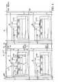
- FIG. 4shows a 2 ⁇ 2 portion of pixel array 200 .
- Pixel array 200comprises a plurality of pixels arranged in a predetermined number of columns and rows. The pixels of each row in array 200 are all turned on at the same time by a row select line, e.g., line 86 (FIG. 4), and the pixels of each column are selectively output by a column select line, e.g., line 42 (FIG. 4). A plurality of rows and column lines are provided for the entire array 200 .
- the row linesare selectively activated by the row driver 210 in response to row address decoder 220 and the column select lines are selectively activated by the column driver 260 in response to column address decoder 270 .
- a row and column addressis provided for each pixel.
- the CMOS imageris operated by the control circuit 250 which controls address decoders 220 , 270 for selecting the appropriate row and column lines for pixel readout, and row and column driver circuitry 210 , 260 which apply driving voltage to the drive transistors of the selected row and column lines.
- FIG. 3shows a simplified timing diagram for the signals used to transfer charge out of photodetector circuit 14 of the FIG. 1 CMOS imager.
- the photogate signal PGis nominally set to 5V and the reset signal RST is nominally set at 2.5V.
- the processis begun at time to by briefly pulsing reset voltage RST to 5V.
- the RST voltagewhich is applied to the gate 32 of reset transistor 31 , causes transistor 31 to turn on and the floating diffusion node 30 to charge to the VDD voltage present at n+ region 34 (less the voltage drop Vth of transistor 31 ). This resets the floating diffusion node 30 to a predetermined voltage (VDD-Vth).
- the charge on floating diffusion node 30is applied to the gate of the source follower transistor 36 to control the current passing through transistor 38 , which has been turned on by a row select (ROW) signal, and load transistor 39 .
- This currentis translated into a voltage on line 42 which is next sampled by providing a SHR signal to the S/H transistor 72 which charges capacitor 74 with the source follower transistor output voltage on line 42 representing the reset charge present at floating diffusion node 30 .
- the PG signalis next pulsed to 0 volts, causing charge to be collected in n+ region 26 .
- a transfer gate voltage pulse TXsimilar to the reset pulse RST, is then applied to transfer gate 28 of transistor 29 to cause the charge in n+ region 26 to transfer to floating diffusion node 30 .
- the transfer gate voltage TXmay be pulsed or held to a fixed DC potential.
- the transfer gate voltage TXmust be pulsed.
- the new output voltage on line 42 generated by source follower transistor 36 currentis then sampled onto capacitor 64 by enabling the sample and hold switch 62 by signal SHS.
- the column select signalis next applied to transistors 68 and 70 and the respective charges stored in capacitors 64 and 74 are subtracted in subtractor 82 to provide a pixel output signal at terminal 81 .
- CMOS imagersmay dispense with the transistor gate 28 and associated transistor 29 or retain these structures while biasing the transfer transistor gate 28 to an always “on” state.
- CMOS imagerThe operation of the charge collection of the CMOS imager is known in the art and is described in several publications such as Mendis et al., “Progress in CMOS Active Pixel Image Sensors,” SPIE Vol. 2172, pp. 19-29 1994; Mendis et al., “CMOS Active Pixel Image Sensors for Highly Integrated Imaging Systems,” IEEE Journal of Solid State Circuits, Vol. 32(2), 1997; and Eric R, Fossum, “CMOS Image Sensors: Electronic Camera on a Chip, IEDM Vol. 95 pages 17-25 (1995) as well as other publications. These references are incorporated herein by reference.
- FIG. 5illustrates a portion of a prior CMOS imager having a photogate as the photoactive area and further includes a transfer gate.
- the imager 100is provided with three doped regions 143 , 126 and 115 , which are doped to a conductivity type different from that of the substrate, for exemplary purposes regions 143 , 126 and 115 are treated as n type, which are within a p-well of a substrate.
- the first doped region 143is the photosite charge collector, and it underlies a portion of the photogate 142 , which is a thin layer of material transparent or partially transparent to radiant energy, such as polysilicon.
- the first doped region 143is typically an n-doped region.
- An insulating layer 140 of silicon dioxide, silicon nitride, or other suitable materialis formed over a surface of the doped layer 143 of the substrate between the photogate 142 and first doped region 143 .
- the second doped region 126transfers charge collected by the photogate 142 and it serves as the source for the transfer transistor 128 .
- the transfer transistor 128includes a transfer gate 139 formed over a gate oxide layer 140 .
- the transfer gate 139has insulating spacers 149 formed on its sides.
- the third doped region 115is the floating diffusion region and is connected to a gate 136 of a source follower transistor by contact lines 125 , 127 , 129 which are typically metal contact lines as described in more detail below.
- the imager 100typically includes a highly n+ doped region 120 within n-doped region 115 under the floating diffusion region contact 125 which provides good ohmic contact of the contact 125 with the n-doped region 115 .
- the floating diffusion contact 125connects n+ region 120 of the floating diffusion region with the gate 136 of the source follower transistor.
- the entire region 115may be doped n+ thereby eliminating the need for n+ region 120 .
- the source and drain regions of the source follower transistorare not seen in FIG. 5 as they are perpendicular to the page but are on either side of gate 136 .
- the source follower gate 136is usually formed of a doped polysilicon which may be silicided and which is deposited over a gate oxide 140 , such as silicon dioxide.
- the floating diffusion contact 125is usually formed of a tungsten plug, typically a Ti/TiN/W metallization stack.
- the floating diffusion contact 125is formed in an insulating layer 135 which is typically an undoped oxide followed by the deposition of a doped oxide such as a BPSG layer deposited over the substrate.
- the tungsten metal which forms the floating diffusion/source follower contact 125is typically deposited using a tungsten fluoride such as WF 6 .
- the layer 135must be etched with a selective dry etch process prior to depositing the tungsten plug connector 125 .
- the imager 100also includes a source follower contact 127 formed in layer 135 in a similar fashion to floating diffusion contact 125 .
- Source follower contact 127is also usually formed of a tungsten plug typically a Ti/TiN/W metallization stack.
- the floating diffusion contact 125 and the source follower contact 127are connected by a metal layer 129 formed over layer 135 .
- metal layer 129is formed of aluminum, copper or any other metal.
- a field oxide layer 132Separating the source follower transistor gate 136 and the floating diffusion region 115 is a field oxide layer 132 , which serves to surround and isolate the cells.
- the field oxide 132may be formed by thermal oxidation of the substrate or in the Local Oxidation of Silicon (LOCOS) or by the Shallow Trench Isolation (STI) process which involves the chemical vapor deposition of an oxide material.
- LOCOSLocal Oxidation of Silicon
- STIShallow Trench Isolation
- FIG. 5shows an imager having a photogate as the photoactive area and additionally includes a transfer transistor
- additional imager structuresare also well known.
- CMOS imagers having a photodiode or a photoconductor as the photoactive areaare known.
- a transfer transistorhas some advantages as described above, it is not required.
- CMOS imagerssuffer dynamic range and charge capacity limitations, and undesirably low signal-to-noise ratios. Attempts to increase charge capacity and improve signal-to-noise ratios have typically focused on using photogate photosensors instead of photodiodes, adding transfer gate stacks to enhance charge transfer, and increasing the size of the photosensor. These methods add process complexity, may limit the use of advantageous features such as silicided gates, and may result in increased pixel cell sizes, thereby reducing pixel array densities.
- the present inventionprovides a CMOS imager having a multiple trench photosensor formed in a doped semiconductor substrate for use in a pixel sensor cell.
- Each trenchcomprises a doped region on the sides and bottom, with a conductive layer formed over the doped region.
- a dielectric layeris preferably formed on the sides and bottom of each trench prior to forming the conductive layer.
- the multi-trench photosensorprovides the photosensitive element with an increased surface area compared to a flat photosensor occupying a comparable area on a substrate.
- the multi-trench photosensoralso exhibits a higher charge capacity, improved dynamic range, and a better signal-to-noise ratio.
- FIG. 1is a representative circuit of a CMOS imager
- FIG. 2is a block diagram of a CMOS active pixel sensor chip
- FIG. 3is a representative timing diagram for the CMOS imager
- FIG. 4is a representative pixel layout showing a 2 ⁇ 2 pixel layout of a CMOS imager
- FIG. 5is a partially cut away side view of a semiconductor imager having a photogate and a transfer gate according to the prior art
- FIG. 6shows a partially cut away side view of a semiconductor imager having a multi-trench photosensor according to the present invention
- FIG. 7shows a partially cut away side view of a semiconductor imager of a first embodiment of the present invention at an intermediate step of processing
- FIG. 8shows a partially cut away side view of a semiconductor imager of the present invention at a processing step subsequent to FIG. 7;
- FIG. 9shows a partially cut away side view of a semiconductor imager of the present invention at a processing step subsequent to FIG. 8;
- FIG. 10shows a partially cut away side view of a semiconductor imager of the present invention at a processing step subsequent to FIG. 9;
- FIG. 11shows a partially cut away side view of a semiconductor imager of the present invention at a processing step subsequent to FIG. 10;
- FIG. 12shows a partially cut away side view of a semiconductor imager of the present invention at a processing step subsequent to FIG. 11;
- FIG. 13shows the wafer of FIG. 7 undergoing an alternative process according to an embodiment of the present invention
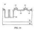
- FIG. 14shows the wafer of FIG. 13 at a processing step subsequent to that shown in FIG. 12;
- FIG. 15is an illustration of a computer system having a CMOS imager according to the present invention.
- wafer and substrateare to be understood as including silicon-on-insulator (SOI) or silicon-on-sapphire (SOS) technology, doped and undoped semiconductors, epitaxial layers of silicon supported by a base semiconductor foundation, and other semiconductor structures.
- SOIsilicon-on-insulator
- SOSsilicon-on-sapphire
- doped and undoped semiconductorsepitaxial layers of silicon supported by a base semiconductor foundation
- previous process stepsmay have been utilized to form regions or junctions in the base semiconductor structure or foundation.
- the semiconductorneed not be silicon-based, but could be based on silicon-germanium, germanium, or gallium arsenide.
- pixelrefers to a picture element unit cell containing a photosensor and transistors for converting electromagnetic radiation to an electrical signal.
- a representative pixelis illustrated in the figures and description herein, and typically fabrication of all pixels in an imager will proceed simultaneously in a similar fashion.
- the following detailed descriptionis, therefore, not to be taken in a limiting sense, and the scope of the present invention is defined by the appended claims.
- a multiple trench photosensorfor use in a pixel sensor cell of a CMOS imager.
- Each trenchcomprises a doped region on the sides and bottom, with a conductive layer formed over the doped region.
- the multi-trench photosensorprovides the photosensitive element with an increased surface area compared to a flat photosensor occupying a comparable area on a substrate.
- the multi-trench photosensoralso exhibits a higher charge capacity, improved dynamic range, and a better signal-to-noise ratio.
- FIG. 6shows a partially cut away cross-sectional view of a CMOS semiconductor wafer according to the present invention. It should be understood that similar reference numbers correspond to similar elements for FIGS. 6-13.
- the structure of the pixel cell 300is shown in more detail in FIG. 6.
- the pixel cell 300may be formed in a substrate 316 having a doped layer or well 311 of a first conductivity type, which for exemplary purposes is treated as a p-type substrate.
- the CMOS imager of the present inventioncan also be fabricated using p-doped regions in an n-well.
- the doped layer 311is provided with three doped regions 326 , 330 and 334 , which are doped to a second conductivity type, which for exemplary purposes is treated as n-type.
- the first doped region 326is the photosite, and it underlies a conductive layer 340 of material transparent to radiant energy, such as polysilicon.
- the photosite 326 and conductive layer 340together form a multi-trench photosensor 324 in accordance with the present invention.
- An insulating layer 328 of silicon dioxide, silicon nitride, ON (oxide-nitride), NO (nitride-oxide), ONO (oxide-nitride-oxide) or other suitable materialis formed between the conductive layer 340 and the photosite 326 .
- a deposited insulating layer 328may extend over a pixel-isolating field region 350 on the opposite side of the photosensor 324 from the transfer gate 352 as illustrated.
- the second doped region 330is the floating diffusion region, sometimes also referred to as a floating diffusion node, and it serves as the source for the reset transistor 354 .
- the third doped region 334is the drain of the reset transistor 354 , and is also connected to voltage source V DD .
- the multi-trench photosensor 324 of the present inventionis manufactured through a process described as follows, and illustrated by FIGS. 7 through 12.
- a substrate 316which may be any of the types of substrates described above, is doped to form a doped substrate layer or well 311 of a first conductivity type, which for exemplary purposes will be described as p-type.
- a field oxide layer 350is formed around the cell 314 at this time, and is shown in FIG. 6 as residing on a side of the photosite 324 opposite the transfer gate 352 and adjacent to the third doped region 334 .
- the field oxide layer 350may be formed by any known technique such as thermal oxidation of the underlying silicon in a LOCOS process or by etching trenches and filling them with oxide in an STI process.
- the reset transistor gate stack 354 and an optional transfer gate stack 352are formed. These include a silicon dioxide or silicon nitride insulator 356 on the doped layer 311 , and a conductive layer 358 of doped polysilicon, tungsten, or other suitable material over the insulating layer 356 .
- Insulating sidewalls 362are also formed on the sides of the gate stacks 352 , 354 . These sidewalls 362 may be formed of, for example, silicon dioxide, silicon nitride, ON, NO or ONO.
- the next stepis to form multiple trenches in the doped layer 311 .
- a resist and mask(not shown) are applied, and photolithographic techniques are used to define the area to be etched-out.
- a directional etching processsuch as Reactive Ion Etching (RIE), or etching with a preferential anisotropic etchant is used to etch into the doped layer 311 to a sufficient depth, e.g., about 0.05 to 10 ⁇ m, to form a pair of trenches 370 a , 370 b . While two trenches 370 a , 370 b are illustrated in FIG. 8, the invention is not so limited and any number of trenches may be formed.
- each trench 370 a , 370 bthe higher the charge storage capacitance of each trench and subsequently of the imager.
- the resist and maskare removed, leaving a structure that appears as shown in FIG. 8.
- the gate stacksmay be formed after the trenches 370 a , 370 b are etched, for exemplary purposes and for convenience etching of the trenches is described as occurring subsequent to gate stack formation.
- the order of these preliminary process stepsmay be varied as is required or convenient for a particular process flow, for example, if a photogate sensor which overlaps the transfer gate is desired, the gate stacks must be formed before the photogate, but if a non-overlapping photogate is desired, the gate stacks are preferably formed after photogate formation.
- fabrication of a photodiode photosensoris greatly simplified if the gate stacks are fabricated before the trench is etched.
- doped regionsare formed in the doped substrate layer 311 by any suitable doping process, such as ion implantation.
- a resist and mask(not shown) are used to shield areas of the layer 311 that are not to be doped.
- Three doped regionsare formed in this step: the photosite 326 , which is formed in the sides and bottom of each trench 370 a , 370 b ; the floating diffusion region 330 ; and a drain region 334 as illustrated in FIG. 10.
- the ion implantation of doped region 326is preferably performed as a series of angled implants, typically four, to assure a more uniformly doped trench sidewall.
- FIG. 9illustrates a resist layer 380 which covers all of the surface of the substrate layer 311 except the trenches 370 a , 370 b , and the region 382 between the trenches 370 a , 370 b , to be doped.
- the implantsare performed at implantation angles ⁇ 1 , that are greater than the critical angle ⁇ C , where each implant is orthogonal to the last implant performed.
- the dose of each implantis between 1 ⁇ 10 12 ions/cm 2 and 1 ⁇ 10 16 ions/cm 2 , preferably between 1 ⁇ 10 13 ions/cm 2 and 1 ⁇ 10 15 ions/cm 2 , and most preferably about 5 ⁇ 10 13 ions/cm 2 .
- the resist 380 and maskare stripped, and a second resist and mask (not shown) are applied. Standard ion implantation is then performed to dope the second and third doped regions 330 , 334 .
- the doped regions 326 , 330 , 334are doped to a second conductivity type, which for exemplary purposes will be considered to be n-type.
- the doping level of the doped regions 326 , 330 , 334may vary but should be of comparable or greater strength than the doping level of the doped layer 311 .
- Doped region 326may be variably doped, such as either n+ or n ⁇ for an n-channel device.
- Doped region 334should be strongly doped, i.e., for an n-channel device, the doped region 334 will be doped as n+.
- Doped region 330is typically strongly doped (n+), and would not be lightly doped (n ⁇ ) unless a buried contact is also used. If desired, multiple masks and resists may be used to dope regions 330 , 334 to different levels.
- an insulating layer 328may now be formed on the sides and bottom of each trench 370 a , 370 b , and the region 382 between the trenches 370 a , 370 b , by chemical vapor deposition, thermal oxidation or other suitable means.
- the insulating layer 382can abut the insulating sidewall 362 of gate stack 352 , or can partially overlap a portion of gate stack 352 as illustrated in FIG. 6.
- the insulating layer 382may be of silicon dioxide, silicon nitride, NO, ON, ONO, or other suitable material, and it has a thickness of approximately 20 to 500 Angstroms for a photogate photosensor. If a photodiode is formed instead of a photogate, the insulating layer 328 would typically be at least 30 Angstroms thick, and may, with the addition of further insulating and passivating layers on the device, be approximately 5 microns thick.
- the final step in the process of the present inventionis to form the photogate 324 .
- the photogate 324has a thin conductive layer 390 that is at least partially transparent to electromagnetic radiation of the wavelengths desired to be sensed.
- the conductive layer 390is of a first conductivity type, and may be doped polysilicon, indium tin oxide, tin oxide, or other suitable material.
- the thickness of the conductive layer 390may be any suitable thickness, e.g., approximately 200 to 4000 Angstroms.
- the conductive layer 390will be formed by CVD or other suitable means, and if the conductive material is a metal compound, CVD, evaporation or sputtering are preferred means of forming the conductive layer 390 .
- the conductive layer 390is formed to cover substantial portions of the insulating layer 328 , and may extend at least partially over the field oxide layer 350 and a portion of the transfer gate 328 .
- the photosensor 324 at this stageis shown in FIG. 12.
- the photosensor 324is essentially complete at this stage, and conventional processing methods may then be used to form contacts and wiring to connect gate lines and other connections in the pixel cell 300 .
- the entire surfacemay then be covered with a passivation layer of, e.g., silicon dioxide, BSG, PSG, or BPSG, which is CMP planarized and etched to provide contact holes, which are then metallized to provide contacts to the photogate, reset gate, and transfer gate.
- a passivation layere.g., silicon dioxide, BSG, PSG, or BPSG
- Conventional multiple layers of conductors and insulatorsmay also be used to interconnect the structures in the manner shown in FIG. 1.
- FIG. 6 and FIGS. 13 and 14An alternative embodiment of the process is illustrated by FIG. 6 and FIGS. 13 and 14. As shown in FIG. 6, this process also begins with a substrate 316 having a doped layer or well 311 of a first conductivity type, e.g., p-type, on which the transfer gate 352 and the reset transistor gate 354 have been formed. Referring now to FIG. 13, the next step in the alternative process is to form doped regions 330 , 334 and a deep doped well 400 in the doped layer 311 .
- a first conductivity typee.g., p-type
- a resist and mask(not shown) are used to expose only the areas to be doped, and a suitable doping process, such as ion implantation, is used to form a deep well 400 of a second conductivity type, e.g., n-type, in the doped layer 311 .
- a suitable doping processsuch as ion implantation
- the doped regions 330 , 334may also be formed at this time by ion implantation or other suitable means.
- the next stepis to form the multiple trenches in the well 400 .
- a resist and mask(not shown) are applied, and photolithographic techniques are used to define the area to be etched-out.
- a directional etching processsuch as Reactive Ion Etching (RIE), or etching with a preferential anisotropic etchant is used to etch into the well 400 to a sufficient depth, e.g., about 0.05 to 10 ⁇ m to form the pair of trenches 370 a , 370 b .
- the depth of the trenchesshould be sufficient to form the photosensor 324 of the present invention therein.
- the resist and maskare removed, leaving a structure that appears as shown in FIG. 14.
- the photosensor 324is then further formed according to the process described above in conjunction with reference to FIGS. 11 and 12.
- Pixel arrays having the photosensors of the present invention, and described with reference to FIGS. 6-14,may be further processed as known in the art to arrive at CMOS imagers having the functions and features of those discussed with reference to FIGS. 1-4 and having the multi-trench photosite of the present invention.
- a typical processor based system which includes a CMOS imager device according to the present inventionis illustrated generally at 500 in FIG. 15.
- a processor based systemis exemplary of a system having digital circuits which could include CMOS imager devices. Without being limiting, such a system could include a computer system, camera system, scanner, machine vision, vehicle navigation, video phone, surveillance system, auto focus system, star tracker system, motion detection system, image stabilization system and data compression system for high-definition television, all of which can utilize the present invention.
- a processor based systemsuch as a computer system, for example generally comprises a central processing unit (CPU) 544 , for example, a microprocessor, that communicates with an input/output (I/O) device 546 over a bus 552 .
- the CMOS imager 542also communicates with the system over bus 552 .
- the computer system 500also includes random access memory (RAM) 548 , and, in the case of a computer system may include peripheral devices such as a floppy disk drive 554 and a compact disk (CD) ROM drive 556 which also communicate with CPU 544 over the bus 552 .
- RAMrandom access memory
- CMOS imager 542is preferably constructed as an integrated circuit which includes pixels containing a photosensor such as a photogate or photodiode formed with multiple trenches, as previously described with respect to FIGS. 6-14. It may also be desirable to integrate the processor 554 , CMOS imager 542 and memory 548 on a single IC chip.
- the present inventionencompasses a photosensor such as a photogate or photodiode formed in multiple trenches.
- the multiple trench photosensorhas an improved charge capacity due to the increase in surface area of the multiple trench photosensor compared to conventional flat photosensors.
Landscapes
- Solid State Image Pick-Up Elements (AREA)
Abstract
Description
- 1. Field of the Invention[0001]
- The invention relates generally to improved semiconductor imaging devices and in particular to a silicon imaging device which can be fabricated using a standard CMOS process. Particularly, the invention relates to a multi-trench region for accumulation of photo-generated charge in a CMOS imager.[0002]
- 2. Discussion of Related Art[0003]
- There are a number of different types of semiconductor-based imagers, including charge coupled devices (CCDs), photodiode arrays, charge injection devices and hybrid focal plane arrays. CCDs are often employed for image acquisition and enjoy a number of advantages which makes it the incumbent technology, particularly for small size imaging applications. CCDs are also capable of large formats with small pixel size and they employ low noise charge domain processing techniques. However, CCD imagers also suffer from a number of disadvantages. For example, they are susceptible to radiation damage, they exhibit destructive read out over time, they require good light shielding to avoid image smear and they have a high power dissipation for large arrays. Additionally, while offering high performance, CCD arrays are difficult to integrate with CMOS processing in part due to a different processing technology and to their high capacitances, complicating the integration of on-chip drive and signal processing electronics with the CCD array. While there has been some attempts to integrate on-chip signal processing with the CCD array, these attempts have not been entirely successful. CCDs also must transfer an image by line charge transfers from pixel to pixel, requiring that the entire array be read out into a memory before individual pixels or groups of pixels can be accessed and processed. This takes time. CCDs may also suffer from incomplete charge transfer from pixel to pixel during charge transfer which also results in image smear.[0004]
- Because of the inherent limitations in CCD technology, there is an interest in CMOS imagers for possible use as low cost imaging devices. A fully compatible CMOS sensor technology enabling a higher level of integration of an image array with associated processing circuits would be beneficial to many digital applications such as, for example, in cameras, scanners, machine vision systems, vehicle navigation systems, video telephones, computer input devices, surveillance systems, auto focus systems, star trackers, motion detection systems, image stabilization systems and data compression systems for high-definition television.[0005]
- The advantages of CMOS imagers over CCD imagers are that CMOS imagers have a low voltage operation and low power consumption; CMOS imagers are compatible with integrated on-chip electronics (control logic and timing, image processing, and signal conditioning such as A/D conversion); CMOS imagers allow random access to the image data; and CMOS imagers have lower fabrication costs as compared with the conventional CCD since standard CMOS processing techniques can be used. Additionally, low power consumption is achieved for CMOS imagers because only one row of pixels at a time needs to be active during the readout and there is no charge transfer (and associated switching) from pixel to pixel during image acquisition. On-chip integration of electronics is particularly advantageous because of the potential to perform many signal conditioning functions in the digital domain (versus analog signal processing) as well as to achieve a reduction in system size and cost.[0006]
- A CMOS imager circuit includes a focal plane array of pixel cells, each one of the cells including either a photogate, a photodiode, or a photoconductor overlying a substrate for accumulating photo-generated charge in the underlying portion of the substrate. A readout circuit is connected to each pixel cell and includes at least an output field effect transistor formed in the substrate and a charge transfer section formed on the substrate adjacent the photogate, photodiode, or the photoconductor having a sensing node, typically a floating diffusion node, connected to the gate of an output transistor. The imager may include at least one electronic device such as a transistor for transferring charge from the underlying portion of the substrate to the floating diffusion node and one device, also typically a transistor, for resetting the node to a predetermined charge level prior to charge transference.[0007]
- In a CMOS imager, the active elements of a pixel cell perform the necessary functions of: (1) photon to charge conversion; (2) accumulation of image charge; (3) transfer of charge to the floating diffusion node accompanied by charge amplification; (4) resetting the floating diffusion node to a known state before the transfer of charge to it; (5) selection of a pixel for readout; and (6) output and amplification of a signal representing pixel charge. Photo charge may be amplified when it moves from the initial charge accumulation region to the floating diffusion node. The charge at the floating diffusion node is typically converted to a pixel output voltage by a source follower output transistor. The photosensitive element of a CMOS imager pixel is typically either a depleted p-n junction photodiode or a field induced depletion region beneath a photogate or a photoconductor. For photodiodes, image lag can be eliminated by completely depleting the photodiode upon readout.[0008]
- CMOS imagers of the type discussed above are generally known as discussed, for example, in Nixon et al., “256×256 CMOS Active Pixel Sensor Camera-on-a-Chip,” IEEE Journal of Solid-State Circuits, Vol. 31(12) pp. 2046-2050, 1996; Mendis et al, “CMOS Active Pixel Image Sensors,” IEEE Transactions on Electron Devices, Vol. 41(3) pp. 452-453, 1994 as well as U.S. Pat. No. 5,708,263 and U.S. Pat. No. 5,471,515, which are herein incorporated by reference.[0009]
- To provide context for the invention, an exemplary CMOS imaging circuit is described below with reference to FIG. 1. The circuit described below, for example, includes a photogate for accumulating photo-generated charge in an underlying portion of the substrate. It should be understood that the CMOS imager may include a photodiode or other image to charge converting device, in lieu of a photogate, as the initial accumulator for photo-generated charge.[0010]
- Reference is now made to FIG. 1 which shows a simplified circuit for a pixel of an exemplary CMOS imager using a photogate and having a[0011]
pixel photodetector circuit 14 and areadout circuit 60. It should be understood that while FIG. 1 shows the circuitry for operation of a single pixel, that in practical use there will be an M×N array of pixels arranged in rows and columns with the pixels of the array accessed using row and column select circuitry, as described in more detail below. - The[0012]
photodetector circuit 14 is shown in part as a cross-sectional view of asemiconductor substrate 16 typically of a p-type silicon, having a surface well of p-type material 20. Anoptional layer 18 of p-type material may be used if desired, but is not required.Substrate 16 may be formed of, for example, Si, SiGe, Ge, and GaAs. Typically theentire substrate 16 is p-type doped silicon substrate and may contain a surface p-well20 (withlayer 18 omitted), but many other options are possible, such as, for example p on p− substrates, p on p+ substrates, p-wells in n-type substrates or the like. The terms wafer or substrate used in the description includes any semiconductor-based structure having an exposed surface in which to form the circuit structure used in the invention. Wafer and substrate are to be understood as including, silicon-on-insulator (SOI) technology, silicon-on-sapphire (SOS) technology, doped and undoped semiconductors, epitaxial layers of silicon supported by a base semiconductor foundation, and other semiconductor structures. Furthermore, when reference is made to a wafer or substrate in the following description, previous process steps may have been utilized to form regions/junctions in the base semiconductor structure or foundation. - An[0013]
insulating layer 22 such as, for example, silicon dioxide is formed on the upper surface of p-well 20. The p-type layer may be a p-well formed insubstrate 16. A photogate24 thin enough to pass radiant energy or of a material which passes radiant energy is formed on theinsulating layer 22. Thephotogate 24 receives an applied control signal PG which causes the initial accumulation of pixel charges inn+ region 26. Then+ type region 26, adjacent one side ofphotogate 24, is formed in the upper surface of p-well 20. Atransfer gate 28 is formed on insulatinglayer 22 betweenn+ type region 26 and a secondn+ type region 30 formed in p-well 20. Then+ regions transfer gate 28 form acharge transfer transistor 29 which is controlled by a transfer signal TX. Then+ region 30 is typically called a floating diffusion region. It is also a node for passing charge accumulated thereat to the gate of asource follower transistor 36 described below. Areset gate 32 is also formed on insulatinglayer 22 adjacent and betweenn+ type region 30 and anothern+ region 34 which is also formed in p-well 20. Thereset gate 32 andn+ regions reset transistor 31 which is controlled by a reset signal RST. Then+ type region 34 is coupled to voltage source VDD. The transfer andreset transistors transfer gate 28 and associatedtransistor 29, this structure provides advantages, but is not required. - [0014]
Photodetector circuit 14 also includes two additional n-channel transistors,source follower transistor 36 and rowselect transistor 38.Transistors transistor 36 also coupled overlead 40 to voltage source VDD and the drain oftransistor 38 coupled to alead 42. The gate oftransistor 36 is coupled overlead 44 ton+ region 30. The drain of rowselect transistor 38 is connected viaconductor 42 to the drains of similar row select transistors for other pixels in a given pixel row. Aload transistor 39 is also coupled between the drain oftransistor 38 and a voltage source VSS.Transistor 39 is kept on by a signal VLN applied to its gate. - The imager includes a[0015]
readout circuit 60 which includes a signal sample and hold (S/H) circuit including a S/H n-channelfield effect transistor 62 and a signal storage capacitor64 connected to thesource follower transistor 36 throughrow transistor 38. The other side of the capacitor64 is connected to a source voltage VSS. The upper side of the capacitor64 is also connected to the gate of a p-channel output transistor 66. The drain of theoutput transistor 66 is connected through a columnselect transistor 68 to a signal sample output node VOUTS and through aload transistor 70 to the voltage supply VDD. A signal called “signal sample and hold” (SHS) briefly turns on the S/H transistor 62 after the charge accumulated beneath thephotogate electrode 24 has been transferred to the floatingdiffusion node 30 and from there to thesource follower transistor 36 and through rowselect transistor 38 toline 42, so that the capacitor64 stores a voltage representing the amount of charge previously accumulated beneath thephotogate electrode 24. - The[0016]
readout circuit 60 also includes a reset sample and hold (S/H) circuit including a S/H transistor72 and a signal storage capacitor74 connected through the S/H transistor72 and through the rowselect transistor 38 to the source of thesource follower transistor 36. The other side of the capacitor74 is connected to the source voltage VSS. The upper side of the capacitor74 is also connected to the gate of a p-channel output transistor 76. The drain of theoutput transistor 76 is connected through a p-channel columnselect transistor 78 to a reset sample output node VOUTR and through aload transistor 80 to the supply voltage VDD. A signal called “reset sample and hold” (SHR) briefly turns on the S/H transistor72 immediately after the reset signal RST has causedreset transistor 31 to turn on and reset the potential of the floatingdiffusion node 30, so that the capacitor74 stores the voltage to which the floatingdiffusion node 30 has been reset. - The[0017]
readout circuit 60 provides correlated sampling of the potential of the floatingdiffusion node 30, first of the reset charge applied tonode 30 byreset transistor 31 and then of the stored charge from thephotogate 24. The two samplings of thediffusion node 30 charges produce respective output voltages VOUTR and VOUTS of thereadout circuit 60. These voltages are then subtracted (VOUTS-VOUTR) bysubtractor 82 to provide anoutput signal terminal 81 which is an image signal independent of pixel to pixel variations caused by fabrication variations in thereset voltage transistor 31 which might cause pixel to pixel variations in the output signal. - FIG. 2 illustrates a block diagram for a CMOS imager having a[0018]
pixel array 200 with each pixel cell being constructed in the manner shown byelement 14 of FIG. 1. FIG. 4 shows a 2×2 portion ofpixel array 200.Pixel array 200 comprises a plurality of pixels arranged in a predetermined number of columns and rows. The pixels of each row inarray 200 are all turned on at the same time by a row select line, e.g., line86 (FIG. 4), and the pixels of each column are selectively output by a column select line, e.g., line42 (FIG. 4). A plurality of rows and column lines are provided for theentire array 200. The row lines are selectively activated by therow driver 210 in response torow address decoder 220 and the column select lines are selectively activated by thecolumn driver 260 in response tocolumn address decoder 270. Thus, a row and column address is provided for each pixel. The CMOS imager is operated by thecontrol circuit 250 which controls addressdecoders column driver circuitry - FIG. 3 shows a simplified timing diagram for the signals used to transfer charge out of[0019]
photodetector circuit 14 of the FIG. 1 CMOS imager. The photogate signal PG is nominally set to 5V and the reset signal RST is nominally set at 2.5V. As can be seen from the figure, the process is begun at time to by briefly pulsing reset voltage RST to 5V. The RST voltage, which is applied to thegate 32 ofreset transistor 31, causestransistor 31 to turn on and the floatingdiffusion node 30 to charge to the VDD voltage present at n+ region34 (less the voltage drop Vth of transistor31). This resets the floatingdiffusion node 30 to a predetermined voltage (VDD-Vth). The charge on floatingdiffusion node 30 is applied to the gate of thesource follower transistor 36 to control the current passing throughtransistor 38, which has been turned on by a row select (ROW) signal, andload transistor 39. This current is translated into a voltage online 42 which is next sampled by providing a SHR signal to the S/H transistor72 which charges capacitor74 with the source follower transistor output voltage online 42 representing the reset charge present at floatingdiffusion node 30. The PG signal is next pulsed to 0 volts, causing charge to be collected inn+ region 26. A transfer gate voltage pulse TX, similar to the reset pulse RST, is then applied to transfergate 28 oftransistor 29 to cause the charge inn+ region 26 to transfer to floatingdiffusion node 30. It should be understood that for the case of a photogate, the transfer gate voltage TX may be pulsed or held to a fixed DC potential. For the implementation of a photodiode with a transfer gate, the transfer gate voltage TX must be pulsed. The new output voltage online 42 generated bysource follower transistor 36 current is then sampled onto capacitor64 by enabling the sample and holdswitch 62 by signal SHS. The column select signal is next applied totransistors subtractor 82 to provide a pixel output signal atterminal 81. It should also be understood that CMOS imagers may dispense with thetransistor gate 28 and associatedtransistor 29 or retain these structures while biasing thetransfer transistor gate 28 to an always “on” state. - The operation of the charge collection of the CMOS imager is known in the art and is described in several publications such as Mendis et al., “Progress in CMOS Active Pixel Image Sensors,” SPIE Vol. 2172, pp. 19-29 1994; Mendis et al., “CMOS Active Pixel Image Sensors for Highly Integrated Imaging Systems,” IEEE Journal of Solid State Circuits, Vol. 32(2), 1997; and Eric R, Fossum, “CMOS Image Sensors: Electronic Camera on a Chip, IEDM Vol. 95 pages 17-25 (1995) as well as other publications. These references are incorporated herein by reference.[0020]
- FIG. 5 illustrates a portion of a prior CMOS imager having a photogate as the photoactive area and further includes a transfer gate. The[0021]
imager 100 is provided with threedoped regions exemplary purposes regions doped region 143 is the photosite charge collector, and it underlies a portion of thephotogate 142, which is a thin layer of material transparent or partially transparent to radiant energy, such as polysilicon. The firstdoped region 143 is typically an n-doped region. An insulatinglayer 140 of silicon dioxide, silicon nitride, or other suitable material is formed over a surface of the dopedlayer 143 of the substrate between the photogate142 and firstdoped region 143. - The second[0022]
doped region 126 transfers charge collected by thephotogate 142 and it serves as the source for thetransfer transistor 128. Thetransfer transistor 128 includes atransfer gate 139 formed over agate oxide layer 140. Thetransfer gate 139 has insulatingspacers 149 formed on its sides. - The third[0023]
doped region 115 is the floating diffusion region and is connected to agate 136 of a source follower transistor bycontact lines imager 100 typically includes a highly n+doped region 120 within n-dopedregion 115 under the floatingdiffusion region contact 125 which provides good ohmic contact of thecontact 125 with the n-dopedregion 115. The floatingdiffusion contact 125 connectsn+ region 120 of the floating diffusion region with thegate 136 of the source follower transistor. In other embodiments of the prior art, theentire region 115 may be doped n+ thereby eliminating the need forn+ region 120. - The source and drain regions of the source follower transistor are not seen in FIG. 5 as they are perpendicular to the page but are on either side of[0024]
gate 136. Thesource follower gate 136 is usually formed of a doped polysilicon which may be silicided and which is deposited over agate oxide 140, such as silicon dioxide. The floatingdiffusion contact 125 is usually formed of a tungsten plug, typically a Ti/TiN/W metallization stack. The floatingdiffusion contact 125 is formed in an insulatinglayer 135 which is typically an undoped oxide followed by the deposition of a doped oxide such as a BPSG layer deposited over the substrate. The tungsten metal which forms the floating diffusion/source follower contact 125 is typically deposited using a tungsten fluoride such as WF6. - Typically, the[0025]
layer 135 must be etched with a selective dry etch process prior to depositing thetungsten plug connector 125. Theimager 100 also includes a source follower contact127 formed inlayer 135 in a similar fashion to floatingdiffusion contact 125. Source follower contact127 is also usually formed of a tungsten plug typically a Ti/TiN/W metallization stack. The floatingdiffusion contact 125 and the source follower contact127 are connected by ametal layer 129 formed overlayer 135. Typicallymetal layer 129 is formed of aluminum, copper or any other metal. - Separating the source[0026]
follower transistor gate 136 and the floatingdiffusion region 115 is afield oxide layer 132, which serves to surround and isolate the cells. Thefield oxide 132 may be formed by thermal oxidation of the substrate or in the Local Oxidation of Silicon (LOCOS) or by the Shallow Trench Isolation (STI) process which involves the chemical vapor deposition of an oxide material. - It should be understood that while FIG. 5 shows an imager having a photogate as the photoactive area and additionally includes a transfer transistor, additional imager structures are also well known. For example, CMOS imagers having a photodiode or a photoconductor as the photoactive area are known. Additionally, while a transfer transistor has some advantages as described above, it is not required.[0027]
- There are drawbacks, however, with prior CMOS imagers. Prior CMOS pixel photosensors suffer dynamic range and charge capacity limitations, and undesirably low signal-to-noise ratios. Attempts to increase charge capacity and improve signal-to-noise ratios have typically focused on using photogate photosensors instead of photodiodes, adding transfer gate stacks to enhance charge transfer, and increasing the size of the photosensor. These methods add process complexity, may limit the use of advantageous features such as silicided gates, and may result in increased pixel cell sizes, thereby reducing pixel array densities.[0028]
- There is a need, therefore, for an improved photosensor for use in an image that exhibits improved dynamic range, a better signal-to-noise ratio, and improved charge capacity for longer integration times.[0029]
- The present invention provides a CMOS imager having a multiple trench photosensor formed in a doped semiconductor substrate for use in a pixel sensor cell. Each trench comprises a doped region on the sides and bottom, with a conductive layer formed over the doped region. For a photogate-type photosensor, a dielectric layer is preferably formed on the sides and bottom of each trench prior to forming the conductive layer.[0030]
- The multi-trench photosensor provides the photosensitive element with an increased surface area compared to a flat photosensor occupying a comparable area on a substrate. The multi-trench photosensor also exhibits a higher charge capacity, improved dynamic range, and a better signal-to-noise ratio.[0031]
- The above and other advantages and features of the invention will be more clearly understood from the following detailed description which is provided in connection with the accompanying drawings.[0032]
- FIG. 1 is a representative circuit of a CMOS imager;[0033]
- FIG. 2 is a block diagram of a CMOS active pixel sensor chip;[0034]
- FIG. 3 is a representative timing diagram for the CMOS imager;[0035]
- FIG. 4 is a representative pixel layout showing a 2×2 pixel layout of a CMOS imager;[0036]
- FIG. 5 is a partially cut away side view of a semiconductor imager having a photogate and a transfer gate according to the prior art;[0037]
- FIG. 6 shows a partially cut away side view of a semiconductor imager having a multi-trench photosensor according to the present invention;[0038]
- FIG. 7 shows a partially cut away side view of a semiconductor imager of a first embodiment of the present invention at an intermediate step of processing;[0039]
- FIG. 8 shows a partially cut away side view of a semiconductor imager of the present invention at a processing step subsequent to FIG. 7;[0040]
- FIG. 9 shows a partially cut away side view of a semiconductor imager of the present invention at a processing step subsequent to FIG. 8;[0041]
- FIG. 10 shows a partially cut away side view of a semiconductor imager of the present invention at a processing step subsequent to FIG. 9;[0042]
- FIG. 11 shows a partially cut away side view of a semiconductor imager of the present invention at a processing step subsequent to FIG. 10;[0043]
- FIG. 12 shows a partially cut away side view of a semiconductor imager of the present invention at a processing step subsequent to FIG. 11;[0044]
- FIG. 13 shows the wafer of FIG. 7 undergoing an alternative process according to an embodiment of the present invention;[0045]
- FIG. 14 shows the wafer of FIG. 13 at a processing step subsequent to that shown in FIG. 12; and[0046]
- FIG. 15 is an illustration of a computer system having a CMOS imager according to the present invention.[0047]
- In the following detailed description, reference is made to the accompanying drawings which form a part hereof, and in which is shown by way of illustration specific embodiments in which the invention may be practiced. These embodiments are described in sufficient detail to enable those skilled in the art to practice the invention, and it is to be understood that other embodiments may be utilized, and that structural, logical and electrical changes may be made without departing from the spirit and scope of the present invention.[0048]
- The terms “wafer” and “substrate” are to be understood as including silicon-on-insulator (SOI) or silicon-on-sapphire (SOS) technology, doped and undoped semiconductors, epitaxial layers of silicon supported by a base semiconductor foundation, and other semiconductor structures. Furthermore, when reference is made to a “wafer” or “substrate” in the following description, previous process steps may have been utilized to form regions or junctions in the base semiconductor structure or foundation. In addition, the semiconductor need not be silicon-based, but could be based on silicon-germanium, germanium, or gallium arsenide.[0049]
- The term “pixel” refers to a picture element unit cell containing a photosensor and transistors for converting electromagnetic radiation to an electrical signal. For purposes of illustration, a representative pixel is illustrated in the figures and description herein, and typically fabrication of all pixels in an imager will proceed simultaneously in a similar fashion. The following detailed description is, therefore, not to be taken in a limiting sense, and the scope of the present invention is defined by the appended claims.[0050]
- In accordance with the present invention, a multiple trench photosensor for use in a pixel sensor cell of a CMOS imager is provided. Each trench comprises a doped region on the sides and bottom, with a conductive layer formed over the doped region. The multi-trench photosensor provides the photosensitive element with an increased surface area compared to a flat photosensor occupying a comparable area on a substrate. The multi-trench photosensor also exhibits a higher charge capacity, improved dynamic range, and a better signal-to-noise ratio.[0051]
- The invention is now described with reference to FIGS. 6-13. FIG. 6 shows a partially cut away cross-sectional view of a CMOS semiconductor wafer according to the present invention. It should be understood that similar reference numbers correspond to similar elements for FIGS. 6-13.[0052]
- The structure of the[0053]
pixel cell 300 according to one embodiment is shown in more detail in FIG. 6. Thepixel cell 300 may be formed in asubstrate 316 having a doped layer or well311 of a first conductivity type, which for exemplary purposes is treated as a p-type substrate. It should be understood that the CMOS imager of the present invention can also be fabricated using p-doped regions in an n-well. The dopedlayer 311 is provided with threedoped regions doped region 326 is the photosite, and it underlies aconductive layer 340 of material transparent to radiant energy, such as polysilicon. Thephotosite 326 andconductive layer 340 together form amulti-trench photosensor 324 in accordance with the present invention. An insulatinglayer 328 of silicon dioxide, silicon nitride, ON (oxide-nitride), NO (nitride-oxide), ONO (oxide-nitride-oxide) or other suitable material is formed between theconductive layer 340 and thephotosite 326. If a deposited insulatinglayer 328 is used (as opposed to a grown layer), it may extend over a pixel-isolatingfield region 350 on the opposite side of the photosensor324 from thetransfer gate 352 as illustrated. The seconddoped region 330 is the floating diffusion region, sometimes also referred to as a floating diffusion node, and it serves as the source for thereset transistor 354. The thirddoped region 334 is the drain of thereset transistor 354, and is also connected to voltage source VDD. - The[0054]
multi-trench photosensor 324 of the present invention is manufactured through a process described as follows, and illustrated by FIGS. 7 through 12. Referring now to FIG. 7, asubstrate 316, which may be any of the types of substrates described above, is doped to form a doped substrate layer or well311 of a first conductivity type, which for exemplary purposes will be described as p-type. Afield oxide layer 350 is formed around thecell 314 at this time, and is shown in FIG. 6 as residing on a side of thephotosite 324 opposite thetransfer gate 352 and adjacent to the thirddoped region 334. Thefield oxide layer 350 may be formed by any known technique such as thermal oxidation of the underlying silicon in a LOCOS process or by etching trenches and filling them with oxide in an STI process. - Next, the reset[0055]
transistor gate stack 354 and an optionaltransfer gate stack 352 are formed. These include a silicon dioxide orsilicon nitride insulator 356 on the dopedlayer 311, and aconductive layer 358 of doped polysilicon, tungsten, or other suitable material over the insulatinglayer 356. Aninsulating cap layer 360 of, for example, silicon dioxide, silicon nitride, ON, NO, or ONO may be formed if desired; also a more conductive layer such as a silicide layer (not shown) may be used between theconductive layer 358 and thecap 360. Insulatingsidewalls 362 are also formed on the sides of the gate stacks352,354. Thesesidewalls 362 may be formed of, for example, silicon dioxide, silicon nitride, ON, NO or ONO. - As shown in FIG. 8, the next step is to form multiple trenches in the doped[0056]
layer 311. A resist and mask (not shown) are applied, and photolithographic techniques are used to define the area to be etched-out. A directional etching process such as Reactive Ion Etching (RIE), or etching with a preferential anisotropic etchant is used to etch into the dopedlayer 311 to a sufficient depth, e.g., about 0.05 to 10 μm, to form a pair oftrenches trenches trench - While the gate stacks may be formed after the[0057]
trenches - IN the next step of the process, illustrated in FIGS. 9 and 10, doped regions are formed in the doped[0058]
substrate layer 311 by any suitable doping process, such as ion implantation. A resist and mask (not shown) are used to shield areas of thelayer 311 that are not to be doped. Three doped regions are formed in this step: thephotosite 326, which is formed in the sides and bottom of eachtrench diffusion region 330; and adrain region 334 as illustrated in FIG. 10. - The ion implantation of doped[0059]
region 326 is preferably performed as a series of angled implants, typically four, to assure a more uniformly doped trench sidewall. FIG. 9 illustrates a resistlayer 380 which covers all of the surface of thesubstrate layer 311 except thetrenches region 382 between thetrenches trenches trench - After formation of the first[0060]
doped region 326, the resist380 and mask are stripped, and a second resist and mask (not shown) are applied. Standard ion implantation is then performed to dope the second and thirddoped regions regions regions layer 311.Doped region 326 may be variably doped, such as either n+ or n− for an n-channel device.Doped region 334 should be strongly doped, i.e., for an n-channel device, the dopedregion 334 will be doped as n+.Doped region 330 is typically strongly doped (n+), and would not be lightly doped (n−) unless a buried contact is also used. If desired, multiple masks and resists may be used todope regions - Referring now to FIG. 11, an insulating[0061]
layer 328 may now be formed on the sides and bottom of eachtrench region 382 between thetrenches layer 382 can abut the insulatingsidewall 362 ofgate stack 352, or can partially overlap a portion ofgate stack 352 as illustrated in FIG. 6. The insulatinglayer 382 may be of silicon dioxide, silicon nitride, NO, ON, ONO, or other suitable material, and it has a thickness of approximately 20 to 500 Angstroms for a photogate photosensor. If a photodiode is formed instead of a photogate, the insulatinglayer 328 would typically be at least 30 Angstroms thick, and may, with the addition of further insulating and passivating layers on the device, be approximately 5 microns thick. - As shown in FIG. 12, the final step in the process of the present invention is to form the[0062]
photogate 324. Thephotogate 324 has a thinconductive layer 390 that is at least partially transparent to electromagnetic radiation of the wavelengths desired to be sensed. Theconductive layer 390 is of a first conductivity type, and may be doped polysilicon, indium tin oxide, tin oxide, or other suitable material. The thickness of theconductive layer 390 may be any suitable thickness, e.g., approximately 200 to 4000 Angstroms. If the conductive material is a silicon material, then theconductive layer 390 will be formed by CVD or other suitable means, and if the conductive material is a metal compound, CVD, evaporation or sputtering are preferred means of forming theconductive layer 390. Theconductive layer 390 is formed to cover substantial portions of the insulatinglayer 328, and may extend at least partially over thefield oxide layer 350 and a portion of thetransfer gate 328. The photosensor324 at this stage is shown in FIG. 12. - For the[0063]
pixel cell 300 of the first embodiment, thephotosensor 324 is essentially complete at this stage, and conventional processing methods may then be used to form contacts and wiring to connect gate lines and other connections in thepixel cell 300. For example, the entire surface may then be covered with a passivation layer of, e.g., silicon dioxide, BSG, PSG, or BPSG, which is CMP planarized and etched to provide contact holes, which are then metallized to provide contacts to the photogate, reset gate, and transfer gate. Conventional multiple layers of conductors and insulators may also be used to interconnect the structures in the manner shown in FIG. 1. - An alternative embodiment of the process is illustrated by FIG. 6 and FIGS. 13 and 14. As shown in FIG. 6, this process also begins with a[0064]
substrate 316 having a doped layer or well311 of a first conductivity type, e.g., p-type, on which thetransfer gate 352 and thereset transistor gate 354 have been formed. Referring now to FIG. 13, the next step in the alternative process is to form dopedregions layer 311. A resist and mask (not shown) are used to expose only the areas to be doped, and a suitable doping process, such as ion implantation, is used to form a deep well400 of a second conductivity type, e.g., n-type, in the dopedlayer 311. The dopedregions - As shown in FIG. 14, the next step is to form the multiple trenches in the[0065]
well 400. A resist and mask (not shown) are applied, and photolithographic techniques are used to define the area to be etched-out. A directional etching process such as Reactive Ion Etching (RIE), or etching with a preferential anisotropic etchant is used to etch into the well400 to a sufficient depth, e.g., about 0.05 to 10 μm to form the pair oftrenches photosensor 324 of the present invention therein. The resist and mask are removed, leaving a structure that appears as shown in FIG. 14. Thephotosensor 324 is then further formed according to the process described above in conjunction with reference to FIGS. 11 and 12. - Pixel arrays having the photosensors of the present invention, and described with reference to FIGS. 6-14, may be further processed as known in the art to arrive at CMOS imagers having the functions and features of those discussed with reference to FIGS. 1-4 and having the multi-trench photosite of the present invention.[0066]
- A typical processor based system which includes a CMOS imager device according to the present invention is illustrated generally at[0067]500 in FIG. 15. A processor based system is exemplary of a system having digital circuits which could include CMOS imager devices. Without being limiting, such a system could include a computer system, camera system, scanner, machine vision, vehicle navigation, video phone, surveillance system, auto focus system, star tracker system, motion detection system, image stabilization system and data compression system for high-definition television, all of which can utilize the present invention.
- A processor based system, such as a computer system, for example generally comprises a central processing unit (CPU)[0068]544, for example, a microprocessor, that communicates with an input/output (I/O)
device 546 over abus 552. TheCMOS imager 542 also communicates with the system overbus 552. Thecomputer system 500 also includes random access memory (RAM)548, and, in the case of a computer system may include peripheral devices such as afloppy disk drive 554 and a compact disk (CD)ROM drive 556 which also communicate withCPU 544 over thebus 552.CMOS imager 542 is preferably constructed as an integrated circuit which includes pixels containing a photosensor such as a photogate or photodiode formed with multiple trenches, as previously described with respect to FIGS. 6-14. It may also be desirable to integrate theprocessor 554,CMOS imager 542 andmemory 548 on a single IC chip. - As can be seen by the embodiments described herein, the present invention encompasses a photosensor such as a photogate or photodiode formed in multiple trenches. The multiple trench photosensor has an improved charge capacity due to the increase in surface area of the multiple trench photosensor compared to conventional flat photosensors.[0069]
- It should be noted that although the invention has been described with specific reference to CMOS imaging circuits having a photogate and a floating diffusion region, the invention has broader applicability and may be used in any CMOS imaging apparatus. Similarly, the process described above is but one method of many that could be used. The above description and drawings illustrate preferred embodiments which achieve the objects, features and advantages of the present invention. Accordingly, the above description and accompanying drawings are only illustrative of preferred embodiments which can achieve the features and advantages of the present invention. It is not intended that the invention be limited to the embodiments shown and described in detail herein. The invention is only limited by the scope of the following claims.[0070]
Claims (8)
1-105. (Cancelled)
106. A method of forming a photosensor, comprising the steps of:
providing a semiconductor substrate having a doped layer of a first conductivity type;
forming a doped region of a second conductivity type in the doped layer;
forming a plurality of trenches in said doped region so that the sides and bottom of each of said plurality of trenches are of the second conductivity type; and
forming an insulating layer on the sides and bottom of each of said plurality of trenches.
107. The method ofclaim 106 , wherein the photosensor is a photodiode sensor.
108. The method ofclaim 106 , further comprising forming a conductive layer on the sides and bottom of each of said plurality of trenches, and wherein the photosensor is a photogate sensor.
109. The method ofclaim 106 , wherein the first conductivity type is p-type, and the second conductivity type is n-type.
110. The method ofclaim 106 , wherein the step of forming a plurality of trenches comprises a reactive ion etching process.
111. The method ofclaim 106 , wherein the doping step comprises ion implantation.
112-116. (Cancelled)
Priority Applications (1)
| Application Number | Priority Date | Filing Date | Title |
|---|---|---|---|
| US10/871,018US7091059B2 (en) | 2000-08-28 | 2004-06-21 | Method of forming a photosensor comprising a plurality of trenches |
Applications Claiming Priority (3)
| Application Number | Priority Date | Filing Date | Title |
|---|---|---|---|
| US09/650,432US6611037B1 (en) | 2000-08-28 | 2000-08-28 | Multi-trench region for accumulation of photo-generated charge in a CMOS imager |
| US10/054,847US6767759B2 (en) | 2000-08-28 | 2002-01-25 | Multi-trench region for accumulation of photo-generated charge in a CMOS imager |
| US10/871,018US7091059B2 (en) | 2000-08-28 | 2004-06-21 | Method of forming a photosensor comprising a plurality of trenches |
Related Parent Applications (1)
| Application Number | Title | Priority Date | Filing Date |
|---|---|---|---|
| US10/054,847DivisionUS6767759B2 (en) | 2000-08-28 | 2002-01-25 | Multi-trench region for accumulation of photo-generated charge in a CMOS imager |
Publications (2)
| Publication Number | Publication Date |
|---|---|
| US20040235216A1true US20040235216A1 (en) | 2004-11-25 |
| US7091059B2 US7091059B2 (en) | 2006-08-15 |
Family
ID=24608881
Family Applications (6)
| Application Number | Title | Priority Date | Filing Date |
|---|---|---|---|
| US09/650,432Expired - LifetimeUS6611037B1 (en) | 2000-08-28 | 2000-08-28 | Multi-trench region for accumulation of photo-generated charge in a CMOS imager |
| US10/054,847Expired - LifetimeUS6767759B2 (en) | 2000-08-28 | 2002-01-25 | Multi-trench region for accumulation of photo-generated charge in a CMOS imager |
| US10/424,807Expired - LifetimeUS6730980B2 (en) | 2000-08-28 | 2003-04-29 | Multi-trench region for accumulation of photo-generated charge in a CMOS imager |
| US10/787,155Expired - LifetimeUS6838742B2 (en) | 2000-08-28 | 2004-02-27 | Multi-trench region for accumulation of photo-generated charge in a CMOS imager |
| US10/871,018Expired - LifetimeUS7091059B2 (en) | 2000-08-28 | 2004-06-21 | Method of forming a photosensor comprising a plurality of trenches |
| US11/001,293Expired - LifetimeUS7279766B2 (en) | 2000-08-28 | 2004-12-02 | Photodiode sensor and photosensor for use in an imaging device |
Family Applications Before (4)
| Application Number | Title | Priority Date | Filing Date |
|---|---|---|---|
| US09/650,432Expired - LifetimeUS6611037B1 (en) | 2000-08-28 | 2000-08-28 | Multi-trench region for accumulation of photo-generated charge in a CMOS imager |
| US10/054,847Expired - LifetimeUS6767759B2 (en) | 2000-08-28 | 2002-01-25 | Multi-trench region for accumulation of photo-generated charge in a CMOS imager |
| US10/424,807Expired - LifetimeUS6730980B2 (en) | 2000-08-28 | 2003-04-29 | Multi-trench region for accumulation of photo-generated charge in a CMOS imager |
| US10/787,155Expired - LifetimeUS6838742B2 (en) | 2000-08-28 | 2004-02-27 | Multi-trench region for accumulation of photo-generated charge in a CMOS imager |
Family Applications After (1)
| Application Number | Title | Priority Date | Filing Date |
|---|---|---|---|
| US11/001,293Expired - LifetimeUS7279766B2 (en) | 2000-08-28 | 2004-12-02 | Photodiode sensor and photosensor for use in an imaging device |
Country Status (1)
| Country | Link |
|---|---|
| US (6) | US6611037B1 (en) |
Cited By (33)
| Publication number | Priority date | Publication date | Assignee | Title |
|---|---|---|---|---|
| US20060043436A1 (en)* | 2004-09-02 | 2006-03-02 | Micron Technology, Inc. | Contacts for CMOS imagers and method of formation |
| US20060081900A1 (en)* | 2004-07-19 | 2006-04-20 | Baggenstoss William J | Pixel cell having a grated interface |
| US7659564B2 (en) | 2006-02-14 | 2010-02-09 | International Business Machines Corporation | CMOS imager photodiode with enhanced capacitance |
| US20100304982A1 (en)* | 2009-05-29 | 2010-12-02 | Ion Torrent Systems, Inc. | Scaffolded nucleic acid polymer particles and methods of making and using |
| US20100301398A1 (en)* | 2009-05-29 | 2010-12-02 | Ion Torrent Systems Incorporated | Methods and apparatus for measuring analytes |
| US8217433B1 (en) | 2010-06-30 | 2012-07-10 | Life Technologies Corporation | One-transistor pixel array |
| US8262900B2 (en) | 2006-12-14 | 2012-09-11 | Life Technologies Corporation | Methods and apparatus for measuring analytes using large scale FET arrays |
| US8264014B2 (en) | 2006-12-14 | 2012-09-11 | Life Technologies Corporation | Methods and apparatus for measuring analytes using large scale FET arrays |
| US8349167B2 (en) | 2006-12-14 | 2013-01-08 | Life Technologies Corporation | Methods and apparatus for detecting molecular interactions using FET arrays |
| US8470164B2 (en) | 2008-06-25 | 2013-06-25 | Life Technologies Corporation | Methods and apparatus for measuring analytes using large scale FET arrays |
| US8653567B2 (en) | 2010-07-03 | 2014-02-18 | Life Technologies Corporation | Chemically sensitive sensor with lightly doped drains |
| US8673627B2 (en) | 2009-05-29 | 2014-03-18 | Life Technologies Corporation | Apparatus and methods for performing electrochemical reactions |
| US8685324B2 (en) | 2010-09-24 | 2014-04-01 | Life Technologies Corporation | Matched pair transistor circuits |
| US8747748B2 (en) | 2012-01-19 | 2014-06-10 | Life Technologies Corporation | Chemical sensor with conductive cup-shaped sensor surface |
| US8753812B2 (en) | 2004-11-12 | 2014-06-17 | The Board Of Trustees Of The Leland Stanford Junior University | Charge perturbation detection method for DNA and other molecules |
| US8776573B2 (en) | 2009-05-29 | 2014-07-15 | Life Technologies Corporation | Methods and apparatus for measuring analytes |
| US8821798B2 (en) | 2012-01-19 | 2014-09-02 | Life Technologies Corporation | Titanium nitride as sensing layer for microwell structure |
| US8858782B2 (en) | 2010-06-30 | 2014-10-14 | Life Technologies Corporation | Ion-sensing charge-accumulation circuits and methods |
| US8936763B2 (en) | 2008-10-22 | 2015-01-20 | Life Technologies Corporation | Integrated sensor arrays for biological and chemical analysis |
| US9080968B2 (en) | 2013-01-04 | 2015-07-14 | Life Technologies Corporation | Methods and systems for point of use removal of sacrificial material |
| US9109251B2 (en) | 2004-06-25 | 2015-08-18 | University Of Hawaii | Ultrasensitive biosensors |
| US9270264B2 (en) | 2012-05-29 | 2016-02-23 | Life Technologies Corporation | System for reducing noise in a chemical sensor array |
| US9618475B2 (en) | 2010-09-15 | 2017-04-11 | Life Technologies Corporation | Methods and apparatus for measuring analytes |
| US9823217B2 (en) | 2013-03-15 | 2017-11-21 | Life Technologies Corporation | Chemical device with thin conductive element |
| US9835585B2 (en) | 2013-03-15 | 2017-12-05 | Life Technologies Corporation | Chemical sensor with protruded sensor surface |
| US9841398B2 (en) | 2013-01-08 | 2017-12-12 | Life Technologies Corporation | Methods for manufacturing well structures for low-noise chemical sensors |
| US9970984B2 (en) | 2011-12-01 | 2018-05-15 | Life Technologies Corporation | Method and apparatus for identifying defects in a chemical sensor array |
| US9995708B2 (en) | 2013-03-13 | 2018-06-12 | Life Technologies Corporation | Chemical sensor with sidewall spacer sensor surface |
| US10100357B2 (en) | 2013-05-09 | 2018-10-16 | Life Technologies Corporation | Windowed sequencing |
| US10422767B2 (en) | 2013-03-15 | 2019-09-24 | Life Technologies Corporation | Chemical sensor with consistent sensor surface areas |
| US10451585B2 (en) | 2009-05-29 | 2019-10-22 | Life Technologies Corporation | Methods and apparatus for measuring analytes |
| US10458942B2 (en) | 2013-06-10 | 2019-10-29 | Life Technologies Corporation | Chemical sensor array having multiple sensors per well |
| US11307166B2 (en) | 2010-07-01 | 2022-04-19 | Life Technologies Corporation | Column ADC |
Families Citing this family (82)
| Publication number | Priority date | Publication date | Assignee | Title |
|---|---|---|---|---|
| US7388289B1 (en)* | 1999-09-02 | 2008-06-17 | Micron Technology, Inc. | Local multilayered metallization |
| US6611037B1 (en)* | 2000-08-28 | 2003-08-26 | Micron Technology, Inc. | Multi-trench region for accumulation of photo-generated charge in a CMOS imager |
| US6906364B2 (en)* | 2001-06-26 | 2005-06-14 | United Microelectronics Corp. | Structure of a CMOS image sensor |
| WO2003017282A1 (en)* | 2001-08-13 | 2003-02-27 | Advanced Micro Devices, Inc. | Memory cell |
| JP4149168B2 (en)* | 2001-11-09 | 2008-09-10 | 株式会社半導体エネルギー研究所 | Light emitting device |
| KR20030096659A (en)* | 2002-06-17 | 2003-12-31 | 삼성전자주식회사 | Pixel array region of an image sensor, structure thereof and fabrication method thereof |
| US6818930B2 (en)* | 2002-11-12 | 2004-11-16 | Micron Technology, Inc. | Gated isolation structure for imagers |
| US6903394B2 (en)* | 2002-11-27 | 2005-06-07 | Micron Technology, Inc. | CMOS imager with improved color response |
| US6780737B2 (en)* | 2002-12-19 | 2004-08-24 | Macronix International Co., Ltd. | Method of manufacturing semiconductor device with buried conductive lines |
| US6974715B2 (en)* | 2002-12-27 | 2005-12-13 | Hynix Semiconductor Inc. | Method for manufacturing CMOS image sensor using spacer etching barrier film |
| US20040164373A1 (en)* | 2003-02-25 | 2004-08-26 | Koester Steven John | Shallow trench isolation structure for strained Si on SiGe |
| US6949445B2 (en)* | 2003-03-12 | 2005-09-27 | Micron Technology, Inc. | Method of forming angled implant for trench isolation |
| KR100955735B1 (en)* | 2003-04-30 | 2010-04-30 | 크로스텍 캐피탈, 엘엘씨 | Unit pixel of CMOS image sensor |
| TWI224463B (en)* | 2003-05-22 | 2004-11-21 | Benq Corp | Calibration method and scan device for transmitted scan |
| US7038232B2 (en)* | 2003-09-24 | 2006-05-02 | Taiwan Semiconductor Manufacturing Co., Ltd. | Quantum efficiency enhancement for CMOS imaging sensor with borderless contact |
| US7420233B2 (en)* | 2003-10-22 | 2008-09-02 | Micron Technology, Inc. | Photodiode for improved transfer gate leakage |
| US7002231B2 (en)* | 2004-02-02 | 2006-02-21 | Micron Technology, Inc. | Barrier regions for image sensors |
| US7902624B2 (en)* | 2004-02-02 | 2011-03-08 | Aptina Imaging Corporation | Barrier regions for image sensors |
| US7154136B2 (en)* | 2004-02-20 | 2006-12-26 | Micron Technology, Inc. | Isolation structures for preventing photons and carriers from reaching active areas and methods of formation |
| US7492027B2 (en)* | 2004-02-20 | 2009-02-17 | Micron Technology, Inc. | Reduced crosstalk sensor and method of formation |
| TWI255673B (en)* | 2004-03-09 | 2006-05-21 | Au Optronics Corp | Flexible printed circuit |
| TWI237905B (en)* | 2004-04-08 | 2005-08-11 | Powerchip Semiconductor Corp | Manufacturing method of photodiode |
| US7076320B1 (en) | 2004-05-04 | 2006-07-11 | Advanced Micro Devices, Inc. | Scatterometry monitor in cluster process tool environment for advanced process control (APC) |
| US7920185B2 (en)* | 2004-06-30 | 2011-04-05 | Micron Technology, Inc. | Shielding black reference pixels in image sensors |
| US7898010B2 (en)* | 2004-07-01 | 2011-03-01 | Micron Technology, Inc. | Transparent conductor based pinned photodiode |
| US7601646B2 (en)* | 2004-07-21 | 2009-10-13 | International Business Machines Corporation | Top-oxide-early process and array top oxide planarization |
| US7297995B2 (en)* | 2004-08-24 | 2007-11-20 | Micron Technology, Inc. | Transparent metal shielded isolation for image sensors |
| US7719583B1 (en)* | 2004-09-07 | 2010-05-18 | Melexis Tessenderlo Nv | Active pixel image sensor with selectable source follower and common source amplifier modes |
| US7253458B2 (en)* | 2004-09-14 | 2007-08-07 | Taiwan Semiconductor Manufacturing Co., Ltd. | CMOS image sensor |
| CN100416866C (en)* | 2004-10-20 | 2008-09-03 | 力晶半导体股份有限公司 | Manufacturing method of photodiode |
| US7221599B1 (en) | 2004-11-01 | 2007-05-22 | Spansion, Llc | Polymer memory cell operation |
| US7098067B2 (en)* | 2004-12-13 | 2006-08-29 | International Business Machines Corporation | Masked sidewall implant for image sensor |
| US7217968B2 (en)* | 2004-12-15 | 2007-05-15 | International Business Machines Corporation | Recessed gate for an image sensor |
| KR100670538B1 (en)* | 2004-12-30 | 2007-01-16 | 매그나칩 반도체 유한회사 | Image sensor and its manufacturing method that can improve optical characteristics |
| US7755116B2 (en)* | 2004-12-30 | 2010-07-13 | Ess Technology, Inc. | Method and apparatus for controlling charge transfer in CMOS sensors with an implant by the transfer gate |
| US7205591B2 (en)* | 2005-04-06 | 2007-04-17 | International Business Machines Corporation | Pixel sensor cell having reduced pinning layer barrier potential and method thereof |
| KR100694470B1 (en)* | 2005-07-11 | 2007-03-12 | 매그나칩 반도체 유한회사 | Image sensor manufacturing method |
| US7141836B1 (en)* | 2005-05-31 | 2006-11-28 | International Business Machines Corporation | Pixel sensor having doped isolation structure sidewall |
| US7375000B2 (en)* | 2005-08-22 | 2008-05-20 | International Business Machines Corporation | Discrete on-chip SOI resistors |
| US7652313B2 (en)* | 2005-11-10 | 2010-01-26 | International Business Machines Corporation | Deep trench contact and isolation of buried photodetectors |
| US7952158B2 (en) | 2007-01-24 | 2011-05-31 | Micron Technology, Inc. | Elevated pocket pixels, imaging devices and systems including the same and method of forming the same |
| US7456452B2 (en)* | 2005-12-15 | 2008-11-25 | Micron Technology, Inc. | Light sensor having undulating features for CMOS imager |
| KR20080104047A (en)* | 2006-03-02 | 2008-11-28 | 아이스모스 테크날러지 코포레이션 | Front electrical contact to photodetector array and method for manufacturing same |
| KR20080100473A (en)* | 2006-03-02 | 2008-11-18 | 아이스모스 테크날러지 코포레이션 | Photodiode having increased proportion of light-sensitive area to ligth-insensitive area |
| JP5110820B2 (en)* | 2006-08-02 | 2012-12-26 | キヤノン株式会社 | Photoelectric conversion device, photoelectric conversion device manufacturing method, and imaging system |
| KR100792342B1 (en)* | 2006-08-23 | 2008-01-07 | 동부일렉트로닉스 주식회사 | Image sensor manufacturing method |
| US7781781B2 (en)* | 2006-11-17 | 2010-08-24 | International Business Machines Corporation | CMOS imager array with recessed dielectric |
| US11339430B2 (en) | 2007-07-10 | 2022-05-24 | Life Technologies Corporation | Methods and apparatus for measuring analytes using large scale FET arrays |
| US7528427B2 (en) | 2007-01-30 | 2009-05-05 | International Business Machines Corporation | Pixel sensor cell having asymmetric transfer gate with reduced pinning layer barrier potential |
| US7459668B2 (en)* | 2007-03-06 | 2008-12-02 | Micron Technology, Inc. | Method, apparatus, and system to reduce ground resistance in a pixel array |
| US7642608B2 (en)* | 2007-03-09 | 2010-01-05 | Aptina Imaging Corporation | Dual isolation for image sensors |
| US7724293B2 (en)* | 2007-03-12 | 2010-05-25 | Aptina Imaging Corporation | Multi-purpose image sensor circuits, imager, system and method of operation |
| US7768047B2 (en)* | 2007-05-10 | 2010-08-03 | Micron Technology, Inc. | Imager element, device and system with recessed transfer gate |
| US20080299700A1 (en)* | 2007-05-28 | 2008-12-04 | Bang-Chiang Lan | Method for fabricating photodiode |
| US7825441B2 (en)* | 2007-06-25 | 2010-11-02 | International Business Machines Corporation | Junction field effect transistor with a hyperabrupt junction |
| JP2009065162A (en)* | 2007-09-07 | 2009-03-26 | Dongbu Hitek Co Ltd | Image sensor and manufacturing method thereof |
| US7858914B2 (en) | 2007-11-20 | 2010-12-28 | Aptina Imaging Corporation | Method and apparatus for reducing dark current and hot pixels in CMOS image sensors |
| US8129764B2 (en) | 2008-06-11 | 2012-03-06 | Aptina Imaging Corporation | Imager devices having differing gate stack sidewall spacers, method for forming such imager devices, and systems including such imager devices |
| JP2010050374A (en)* | 2008-08-25 | 2010-03-04 | Seiko Instruments Inc | Semiconductor device |
| JP5394791B2 (en) | 2009-03-27 | 2014-01-22 | 浜松ホトニクス株式会社 | Back-thinned solid-state image sensor |
| JP2010287743A (en)* | 2009-06-11 | 2010-12-24 | Sony Corp | Semiconductor device and manufacturing method thereof, solid-state imaging device |
| TWI539172B (en) | 2010-06-30 | 2016-06-21 | 生命技術公司 | Methods and apparatus for testing isfet arrays |
| JP5726005B2 (en)* | 2010-08-02 | 2015-05-27 | アイメックImec | Method for manufacturing CMOS imaging device array |
| KR101867337B1 (en)* | 2012-01-30 | 2018-06-15 | 삼성전자주식회사 | An image sensor and method of manufacturing the same |
| US8962366B2 (en) | 2013-01-28 | 2015-02-24 | Life Technologies Corporation | Self-aligned well structures for low-noise chemical sensors |
| US8841217B1 (en) | 2013-03-13 | 2014-09-23 | Life Technologies Corporation | Chemical sensor with protruded sensor surface |
| EP2972279B1 (en) | 2013-03-15 | 2021-10-06 | Life Technologies Corporation | Chemical sensors with consistent sensor surface areas |
| US9116117B2 (en) | 2013-03-15 | 2015-08-25 | Life Technologies Corporation | Chemical sensor with sidewall sensor surface |
| JP6465545B2 (en) | 2013-09-27 | 2019-02-06 | ソニー株式会社 | Imaging device, manufacturing method thereof, and electronic apparatus |
| FR3011678B1 (en)* | 2013-10-07 | 2017-01-27 | St Microelectronics Crolles 2 Sas | METHOD FOR RELAXING MECHANICAL CROSS-VOLTAGE CONSTRAINTS IN THE ACTIVE REGION OF A MOS TRANSISTOR, AND CORRESPONDING INTEGRATED CIRCUIT |
| KR102244679B1 (en) | 2014-07-15 | 2021-04-27 | 삼성전자주식회사 | Image sensor and method of operating the image sensor |
| DE102014113037B4 (en)* | 2014-09-10 | 2018-02-08 | Infineon Technologies Ag | Imaging circuits and a method of operating an imaging circuit |
| US10077472B2 (en) | 2014-12-18 | 2018-09-18 | Life Technologies Corporation | High data rate integrated circuit with power management |
| KR102593647B1 (en) | 2014-12-18 | 2023-10-26 | 라이프 테크놀로지스 코포레이션 | High data rate integrated circuit with transmitter configuration |
| CN107407656B (en) | 2014-12-18 | 2020-04-07 | 生命科技公司 | Method and apparatus for measuring analytes using large scale FET arrays |
| US9584744B2 (en)* | 2015-06-23 | 2017-02-28 | Semiconductor Components Industries, Llc | Image sensors with voltage-biased trench isolation structures |
| CN106981495B (en)* | 2016-01-15 | 2019-10-25 | 中芯国际集成电路制造(上海)有限公司 | A kind of CMOS image sensor and its manufacturing method |
| US10515989B2 (en)* | 2017-08-30 | 2019-12-24 | Taiwan Semiconductor Manufacturing Co., Ltd. | Device comprising photodiode and method of making the same |
| KR102498503B1 (en)* | 2018-09-05 | 2023-02-09 | 삼성전자주식회사 | Image sensor |
| US11495631B2 (en) | 2020-02-07 | 2022-11-08 | Sensors Unlimited, Inc. | Pin mesa diodes with over-current protection |
| US20230215885A1 (en)* | 2021-12-30 | 2023-07-06 | Shenzhen GOODIX Technology Co., Ltd. | Adjustable well capacity pixel for semiconductor imaging sensors |
| WO2025140564A1 (en)* | 2023-12-28 | 2025-07-03 | 上海联影微电子科技有限公司 | Photodiode and manufacturing method therefor, and electronic element |
Citations (35)
| Publication number | Priority date | Publication date | Assignee | Title |
|---|---|---|---|---|
| US4374700A (en)* | 1981-05-29 | 1983-02-22 | Texas Instruments Incorporated | Method of manufacturing silicide contacts for CMOS devices |
| US4803359A (en)* | 1983-05-16 | 1989-02-07 | Fuji Photo Film Co., Ltd. | Method for detecting radiation image |
| US4972244A (en)* | 1988-06-16 | 1990-11-20 | Commissariat A L'energie Atomique | Photodiode and photodiode array on a II-VI material and processes for the production thereof |
| US5055900A (en)* | 1989-10-11 | 1991-10-08 | The Trustees Of Columbia University In The City Of New York | Trench-defined charge-coupled device |
| US5112762A (en)* | 1990-12-05 | 1992-05-12 | Anderson Dirk N | High angle implant around top of trench to reduce gated diode leakage |
| US5151385A (en)* | 1982-12-16 | 1992-09-29 | Hitachi, Ltd. | Method of manufacturing a metallic silicide transparent electrode |
| US5173756A (en)* | 1990-01-05 | 1992-12-22 | International Business Machines Corporation | Trench charge-coupled device |
| US5223726A (en)* | 1989-07-25 | 1993-06-29 | Matsushita Electric Industrial Co., Ltd. | Semiconductor device for charge transfer device |
| US5239193A (en)* | 1990-04-02 | 1993-08-24 | At&T Bell Laboratories | Silicon photodiode for monolithic integrated circuits |
| US5319604A (en)* | 1990-05-08 | 1994-06-07 | Texas Instruments Incorporated | Circuitry and method for selectively switching negative voltages in CMOS integrated circuits |
| US5461425A (en)* | 1994-02-15 | 1995-10-24 | Stanford University | CMOS image sensor with pixel level A/D conversion |
| US5471515A (en)* | 1994-01-28 | 1995-11-28 | California Institute Of Technology | Active pixel sensor with intra-pixel charge transfer |
| US5541402A (en)* | 1994-10-17 | 1996-07-30 | At&T Corp. | Imaging active pixel device having a non-destructive read-out gate |
| US5576763A (en)* | 1994-11-22 | 1996-11-19 | Lucent Technologies Inc. | Single-polysilicon CMOS active pixel |
| US5608243A (en)* | 1995-10-19 | 1997-03-04 | National Semiconductor Corporation | Single split-gate MOS transistor active pixel sensor cell with automatic anti-blooming and wide dynamic range |
| US5614744A (en)* | 1995-08-04 | 1997-03-25 | National Semiconductor Corporation | CMOS-based, low leakage active pixel array with anti-blooming isolation |
| US5625210A (en)* | 1995-04-13 | 1997-04-29 | Eastman Kodak Company | Active pixel sensor integrated with a pinned photodiode |
| US5705846A (en)* | 1995-07-31 | 1998-01-06 | National Semiconductor Corporation | CMOS-compatible active pixel image array using vertical pnp cell |
| US5708263A (en)* | 1995-12-27 | 1998-01-13 | International Business Machines Corporation | Photodetector array |
| US5721425A (en)* | 1996-03-01 | 1998-02-24 | National Semiconductor Corporation | Active pixel sensor cell that reduces the effect of 1/f noise, increases the voltage range of the cell, and reduces the size of the cell |
| US5731622A (en)* | 1996-02-28 | 1998-03-24 | Nec Corporation | Semiconductor photodiode |
| US5747840A (en)* | 1996-10-21 | 1998-05-05 | Foveonics, Inc. | Photodiode with improved photoresponse behavior |
| US5757045A (en)* | 1996-07-17 | 1998-05-26 | Taiwan Semiconductor Manufacturing Company Ltd. | CMOS device structure with reduced risk of salicide bridging and reduced resistance via use of a ultra shallow, junction extension, ion implantation |
| US5770878A (en)* | 1996-04-10 | 1998-06-23 | Harris Corporation | Trench MOS gate device |
| US5990515A (en)* | 1998-03-30 | 1999-11-23 | Advanced Micro Devices, Inc. | Trenched gate non-volatile semiconductor device and method with corner doping and sidewall doping |
| US5994751A (en)* | 1995-08-03 | 1999-11-30 | Siemens Aktiengesellschaft | Photodiode having reduced series resistance, and method for fabrication thereof |
| US6001684A (en)* | 1997-06-04 | 1999-12-14 | Siemens Aktiengesellschaft | Method for forming a capacitor |
| US6008103A (en)* | 1998-02-27 | 1999-12-28 | Siemens Aktiengesellschaft | Method for forming trench capacitors in an integrated circuit |
| US6051852A (en)* | 1995-03-31 | 2000-04-18 | Eastman Kodak Company | Self aligned LOD antiblooming structure for solid-state imagers |
| US6118142A (en)* | 1998-11-09 | 2000-09-12 | United Microelectronics Corp. | CMOS sensor |
| US6232626B1 (en)* | 1999-02-01 | 2001-05-15 | Micron Technology, Inc. | Trench photosensor for a CMOS imager |
| US6300648B1 (en)* | 1999-12-28 | 2001-10-09 | Xerox Corporation | Continuous amorphous silicon layer sensors using sealed metal back contact |
| US6593616B2 (en)* | 1999-12-06 | 2003-07-15 | Micron Technology Inc. | Buried bit line memory circuitry |
| US6611037B1 (en)* | 2000-08-28 | 2003-08-26 | Micron Technology, Inc. | Multi-trench region for accumulation of photo-generated charge in a CMOS imager |
| US20050227402A1 (en)* | 2004-04-08 | 2005-10-13 | Ko-Hsing Chang | [method of manufacturing photodiode] |
Family Cites Families (5)
| Publication number | Priority date | Publication date | Assignee | Title |
|---|---|---|---|---|
| US4352948A (en)* | 1979-09-07 | 1982-10-05 | Massachusetts Institute Of Technology | High-intensity solid-state solar-cell device |
| JP2775990B2 (en)* | 1990-05-08 | 1998-07-16 | 松下電器産業株式会社 | Method for manufacturing semiconductor device |
| JP3247163B2 (en)* | 1992-09-14 | 2002-01-15 | 株式会社東芝 | Solid-state imaging device and manufacturing method thereof |
| KR0186195B1 (en)* | 1995-12-11 | 1999-05-01 | 문정환 | Color linear charge coupled device and driving method thereof |
| US6339248B1 (en)* | 1999-11-15 | 2002-01-15 | Omnivision Technologies, Inc. | Optimized floating P+ region photodiode for a CMOS image sensor |
- 2000
- 2000-08-28USUS09/650,432patent/US6611037B1/ennot_activeExpired - Lifetime
- 2002
- 2002-01-25USUS10/054,847patent/US6767759B2/ennot_activeExpired - Lifetime
- 2003
- 2003-04-29USUS10/424,807patent/US6730980B2/ennot_activeExpired - Lifetime
- 2004
- 2004-02-27USUS10/787,155patent/US6838742B2/ennot_activeExpired - Lifetime
- 2004-06-21USUS10/871,018patent/US7091059B2/ennot_activeExpired - Lifetime
- 2004-12-02USUS11/001,293patent/US7279766B2/ennot_activeExpired - Lifetime
Patent Citations (38)
| Publication number | Priority date | Publication date | Assignee | Title |
|---|---|---|---|---|
| US4374700A (en)* | 1981-05-29 | 1983-02-22 | Texas Instruments Incorporated | Method of manufacturing silicide contacts for CMOS devices |
| US5151385A (en)* | 1982-12-16 | 1992-09-29 | Hitachi, Ltd. | Method of manufacturing a metallic silicide transparent electrode |
| US4803359A (en)* | 1983-05-16 | 1989-02-07 | Fuji Photo Film Co., Ltd. | Method for detecting radiation image |
| US4972244A (en)* | 1988-06-16 | 1990-11-20 | Commissariat A L'energie Atomique | Photodiode and photodiode array on a II-VI material and processes for the production thereof |
| US5223726A (en)* | 1989-07-25 | 1993-06-29 | Matsushita Electric Industrial Co., Ltd. | Semiconductor device for charge transfer device |
| US5055900A (en)* | 1989-10-11 | 1991-10-08 | The Trustees Of Columbia University In The City Of New York | Trench-defined charge-coupled device |
| US5173756A (en)* | 1990-01-05 | 1992-12-22 | International Business Machines Corporation | Trench charge-coupled device |
| US5239193A (en)* | 1990-04-02 | 1993-08-24 | At&T Bell Laboratories | Silicon photodiode for monolithic integrated circuits |
| US5319604A (en)* | 1990-05-08 | 1994-06-07 | Texas Instruments Incorporated | Circuitry and method for selectively switching negative voltages in CMOS integrated circuits |
| US5112762A (en)* | 1990-12-05 | 1992-05-12 | Anderson Dirk N | High angle implant around top of trench to reduce gated diode leakage |
| US5471515A (en)* | 1994-01-28 | 1995-11-28 | California Institute Of Technology | Active pixel sensor with intra-pixel charge transfer |
| US5461425A (en)* | 1994-02-15 | 1995-10-24 | Stanford University | CMOS image sensor with pixel level A/D conversion |
| US5541402A (en)* | 1994-10-17 | 1996-07-30 | At&T Corp. | Imaging active pixel device having a non-destructive read-out gate |
| US5576763A (en)* | 1994-11-22 | 1996-11-19 | Lucent Technologies Inc. | Single-polysilicon CMOS active pixel |
| US6051852A (en)* | 1995-03-31 | 2000-04-18 | Eastman Kodak Company | Self aligned LOD antiblooming structure for solid-state imagers |
| US5625210A (en)* | 1995-04-13 | 1997-04-29 | Eastman Kodak Company | Active pixel sensor integrated with a pinned photodiode |
| US5705846A (en)* | 1995-07-31 | 1998-01-06 | National Semiconductor Corporation | CMOS-compatible active pixel image array using vertical pnp cell |
| US5994751A (en)* | 1995-08-03 | 1999-11-30 | Siemens Aktiengesellschaft | Photodiode having reduced series resistance, and method for fabrication thereof |
| US5614744A (en)* | 1995-08-04 | 1997-03-25 | National Semiconductor Corporation | CMOS-based, low leakage active pixel array with anti-blooming isolation |
| US5608243A (en)* | 1995-10-19 | 1997-03-04 | National Semiconductor Corporation | Single split-gate MOS transistor active pixel sensor cell with automatic anti-blooming and wide dynamic range |
| US5708263A (en)* | 1995-12-27 | 1998-01-13 | International Business Machines Corporation | Photodetector array |
| US5731622A (en)* | 1996-02-28 | 1998-03-24 | Nec Corporation | Semiconductor photodiode |
| US5721425A (en)* | 1996-03-01 | 1998-02-24 | National Semiconductor Corporation | Active pixel sensor cell that reduces the effect of 1/f noise, increases the voltage range of the cell, and reduces the size of the cell |
| US5770878A (en)* | 1996-04-10 | 1998-06-23 | Harris Corporation | Trench MOS gate device |
| US5757045A (en)* | 1996-07-17 | 1998-05-26 | Taiwan Semiconductor Manufacturing Company Ltd. | CMOS device structure with reduced risk of salicide bridging and reduced resistance via use of a ultra shallow, junction extension, ion implantation |
| US5747840A (en)* | 1996-10-21 | 1998-05-05 | Foveonics, Inc. | Photodiode with improved photoresponse behavior |
| US6001684A (en)* | 1997-06-04 | 1999-12-14 | Siemens Aktiengesellschaft | Method for forming a capacitor |
| US6008103A (en)* | 1998-02-27 | 1999-12-28 | Siemens Aktiengesellschaft | Method for forming trench capacitors in an integrated circuit |
| US5990515A (en)* | 1998-03-30 | 1999-11-23 | Advanced Micro Devices, Inc. | Trenched gate non-volatile semiconductor device and method with corner doping and sidewall doping |
| US6118142A (en)* | 1998-11-09 | 2000-09-12 | United Microelectronics Corp. | CMOS sensor |
| US6232626B1 (en)* | 1999-02-01 | 2001-05-15 | Micron Technology, Inc. | Trench photosensor for a CMOS imager |
| US6500692B1 (en)* | 1999-02-01 | 2002-12-31 | Micron Technology, Inc. | Method of making trench photosensor for a CMOS imager |
| US6593616B2 (en)* | 1999-12-06 | 2003-07-15 | Micron Technology Inc. | Buried bit line memory circuitry |
| US6300648B1 (en)* | 1999-12-28 | 2001-10-09 | Xerox Corporation | Continuous amorphous silicon layer sensors using sealed metal back contact |
| US6611037B1 (en)* | 2000-08-28 | 2003-08-26 | Micron Technology, Inc. | Multi-trench region for accumulation of photo-generated charge in a CMOS imager |
| US6730980B2 (en)* | 2000-08-28 | 2004-05-04 | Micron Technology, Inc. | Multi-trench region for accumulation of photo-generated charge in a CMOS imager |
| US6767759B2 (en)* | 2000-08-28 | 2004-07-27 | Micron Technology, Inc. | Multi-trench region for accumulation of photo-generated charge in a CMOS imager |
| US20050227402A1 (en)* | 2004-04-08 | 2005-10-13 | Ko-Hsing Chang | [method of manufacturing photodiode] |
Cited By (118)
| Publication number | Priority date | Publication date | Assignee | Title |
|---|---|---|---|---|
| US10563252B2 (en) | 2004-06-25 | 2020-02-18 | University Of Hawaii | Ultrasensitive biosensors |
| US9109251B2 (en) | 2004-06-25 | 2015-08-18 | University Of Hawaii | Ultrasensitive biosensors |
| US8101454B2 (en)* | 2004-07-19 | 2012-01-24 | Micron Technology, Inc. | Method of forming pixel cell having a grated interface |
| US20060081900A1 (en)* | 2004-07-19 | 2006-04-20 | Baggenstoss William J | Pixel cell having a grated interface |
| US7498188B2 (en)* | 2004-09-02 | 2009-03-03 | Aptina Imaging Corporation | Contacts for CMOS imagers and method of formation |
| US20090184345A1 (en)* | 2004-09-02 | 2009-07-23 | Xiaofeng Fan | Contacts for cmos imagers and method of formation |
| US20060043436A1 (en)* | 2004-09-02 | 2006-03-02 | Micron Technology, Inc. | Contacts for CMOS imagers and method of formation |
| US8129761B2 (en)* | 2004-09-02 | 2012-03-06 | Aptina Imaging Corporation | Contacts for CMOS imagers and method of formation |
| US12139749B2 (en) | 2004-11-12 | 2024-11-12 | The Board Of Trustees Of The Leland Stanford Junior University | Charge perturbation detection system for DNA and other molecules |
| US8753812B2 (en) | 2004-11-12 | 2014-06-17 | The Board Of Trustees Of The Leland Stanford Junior University | Charge perturbation detection method for DNA and other molecules |
| US9228971B2 (en) | 2004-11-12 | 2016-01-05 | The Board Of Trustees Of The Leland Stanford Junior University | Charge perturbation detection system for DNA and other molecules |
| US10822641B2 (en) | 2004-11-12 | 2020-11-03 | The Board Of Trustees Of The Leland Stanford Junior University | Charge perturbation detection system for DNA and other molecules |
| US8106432B2 (en) | 2006-02-14 | 2012-01-31 | International Business Machines Corporation | CMOS imager photodiode with enhanced capacitance |
| US8440490B2 (en) | 2006-02-14 | 2013-05-14 | International Business Machines Corporation | CMOS imager photodiode with enhanced capacitance |
| US20100084690A1 (en)* | 2006-02-14 | 2010-04-08 | International Business Machines Corporation | Cmos imager photodiode with enhanced capacitance |
| US7659564B2 (en) | 2006-02-14 | 2010-02-09 | International Business Machines Corporation | CMOS imager photodiode with enhanced capacitance |
| US10203300B2 (en) | 2006-12-14 | 2019-02-12 | Life Technologies Corporation | Methods and apparatus for measuring analytes using large scale FET arrays |
| US8535513B2 (en) | 2006-12-14 | 2013-09-17 | Life Technologies Corporation | Methods and apparatus for measuring analytes using large scale FET arrays |
| US8306757B2 (en) | 2006-12-14 | 2012-11-06 | Life Technologies Corporation | Methods and apparatus for measuring analytes using large scale FET arrays |
| US8313639B2 (en) | 2006-12-14 | 2012-11-20 | Life Technologies Corporation | Methods and apparatus for measuring analytes using large scale FET arrays |
| US8313625B2 (en) | 2006-12-14 | 2012-11-20 | Life Technologies Corporation | Methods and apparatus for measuring analytes using large scale FET arrays |
| US8317999B2 (en) | 2006-12-14 | 2012-11-27 | Life Technologies Corporation | Methods and apparatus for measuring analytes using large scale FET arrays |
| US8349167B2 (en) | 2006-12-14 | 2013-01-08 | Life Technologies Corporation | Methods and apparatus for detecting molecular interactions using FET arrays |
| US8415716B2 (en) | 2006-12-14 | 2013-04-09 | Life Technologies Corporation | Chemically sensitive sensors with feedback circuits |
| US8269261B2 (en) | 2006-12-14 | 2012-09-18 | Life Technologies Corporation | Methods and apparatus for measuring analytes using large scale FET arrays |
| US9039888B2 (en) | 2006-12-14 | 2015-05-26 | Life Technologies Corporation | Methods and apparatus for detecting molecular interactions using FET arrays |
| US8264014B2 (en) | 2006-12-14 | 2012-09-11 | Life Technologies Corporation | Methods and apparatus for measuring analytes using large scale FET arrays |
| US8426898B2 (en) | 2006-12-14 | 2013-04-23 | Life Technologies Corporation | Methods and apparatus for measuring analytes using large scale FET arrays |
| US8426899B2 (en) | 2006-12-14 | 2013-04-23 | Life Technologies Corporation | Methods and apparatus for measuring analytes using large scale FET arrays |
| US8262900B2 (en) | 2006-12-14 | 2012-09-11 | Life Technologies Corporation | Methods and apparatus for measuring analytes using large scale FET arrays |
| US8293082B2 (en) | 2006-12-14 | 2012-10-23 | Life Technologies Corporation | Methods and apparatus for measuring analytes using large scale FET arrays |
| US8435395B2 (en) | 2006-12-14 | 2013-05-07 | Life Technologies Corporation | Methods and apparatus for measuring analytes using large scale FET arrays |
| US8764969B2 (en) | 2006-12-14 | 2014-07-01 | Life Technologies Corporation | Methods for operating chemically sensitive sensors with sample and hold capacitors |
| US8441044B2 (en) | 2006-12-14 | 2013-05-14 | Life Technologies Corporation | Methods for manufacturing low noise chemically-sensitive field effect transistors |
| US8445945B2 (en) | 2006-12-14 | 2013-05-21 | Life Technologies Corporation | Low noise chemically-sensitive field effect transistors |
| US8450781B2 (en) | 2006-12-14 | 2013-05-28 | Life Technologies Corporation | Methods and apparatus for measuring analytes using large scale FET arrays |
| US8658017B2 (en) | 2006-12-14 | 2014-02-25 | Life Technologies Corporation | Methods for operating an array of chemically-sensitive sensors |
| US8685230B2 (en) | 2006-12-14 | 2014-04-01 | Life Technologies Corporation | Methods and apparatus for high-speed operation of a chemically-sensitive sensor array |
| US9989489B2 (en) | 2006-12-14 | 2018-06-05 | Life Technnologies Corporation | Methods for calibrating an array of chemically-sensitive sensors |
| US8492799B2 (en) | 2006-12-14 | 2013-07-23 | Life Technologies Corporation | Methods and apparatus for detecting molecular interactions using FET arrays |
| US8492800B2 (en) | 2006-12-14 | 2013-07-23 | Life Technologies Corporation | Chemically sensitive sensors with sample and hold capacitors |
| US8496802B2 (en) | 2006-12-14 | 2013-07-30 | Life Technologies Corporation | Methods for operating chemically-sensitive sample and hold sensors |
| US8502278B2 (en) | 2006-12-14 | 2013-08-06 | Life Technologies Corporation | Chemically-sensitive sample and hold sensors |
| US8519448B2 (en) | 2006-12-14 | 2013-08-27 | Life Technologies Corporation | Chemically-sensitive array with active and reference sensors |
| US8575664B2 (en) | 2006-12-14 | 2013-11-05 | Life Technologies Corporation | Chemically-sensitive sensor array calibration circuitry |
| US9404920B2 (en) | 2006-12-14 | 2016-08-02 | Life Technologies Corporation | Methods and apparatus for detecting molecular interactions using FET arrays |
| US8530941B2 (en) | 2006-12-14 | 2013-09-10 | Life Technologies Corporation | Methods and apparatus for measuring analytes using large scale FET arrays |
| US9951382B2 (en) | 2006-12-14 | 2018-04-24 | Life Technologies Corporation | Methods and apparatus for measuring analytes using large scale FET arrays |
| US8540867B2 (en) | 2006-12-14 | 2013-09-24 | Life Technologies Corporation | Methods and apparatus for detecting molecular interactions using FET arrays |
| US8540865B2 (en) | 2006-12-14 | 2013-09-24 | Life Technologies Corporation | Methods and apparatus for detecting molecular interactions using FET arrays |
| US8540868B2 (en) | 2006-12-14 | 2013-09-24 | Life Technologies Corporation | Methods and apparatus for detecting molecular interactions using FET arrays |
| US8540866B2 (en) | 2006-12-14 | 2013-09-24 | Life Technologies Corporation | Methods and apparatus for detecting molecular interactions using FET arrays |
| US8558288B2 (en) | 2006-12-14 | 2013-10-15 | Life Technologies Corporation | Methods and apparatus for measuring analytes using large scale FET arrays |
| US8524057B2 (en) | 2008-06-25 | 2013-09-03 | Life Technologies Corporation | Methods and apparatus for measuring analytes using large scale FET arrays |
| US8470164B2 (en) | 2008-06-25 | 2013-06-25 | Life Technologies Corporation | Methods and apparatus for measuring analytes using large scale FET arrays |
| US9964515B2 (en) | 2008-10-22 | 2018-05-08 | Life Technologies Corporation | Integrated sensor arrays for biological and chemical analysis |
| US8936763B2 (en) | 2008-10-22 | 2015-01-20 | Life Technologies Corporation | Integrated sensor arrays for biological and chemical analysis |
| US10451585B2 (en) | 2009-05-29 | 2019-10-22 | Life Technologies Corporation | Methods and apparatus for measuring analytes |
| US8592153B1 (en) | 2009-05-29 | 2013-11-26 | Life Technologies Corporation | Methods for manufacturing high capacitance microwell structures of chemically-sensitive sensors |
| US8673627B2 (en) | 2009-05-29 | 2014-03-18 | Life Technologies Corporation | Apparatus and methods for performing electrochemical reactions |
| US9927393B2 (en) | 2009-05-29 | 2018-03-27 | Life Technologies Corporation | Methods and apparatus for measuring analytes |
| US8592154B2 (en) | 2009-05-29 | 2013-11-26 | Life Technologies Corporation | Methods and apparatus for high speed operation of a chemically-sensitive sensor array |
| US8698212B2 (en) | 2009-05-29 | 2014-04-15 | Life Technologies Corporation | Active chemically-sensitive sensors |
| US8574835B2 (en) | 2009-05-29 | 2013-11-05 | Life Technologies Corporation | Scaffolded nucleic acid polymer particles and methods of making and using |
| US8742469B2 (en) | 2009-05-29 | 2014-06-03 | Life Technologies Corporation | Active chemically-sensitive sensors with correlated double sampling |
| US12234452B2 (en) | 2009-05-29 | 2025-02-25 | Life Technologies Corporation | Scaffolded nucleic acid polymer particles and methods of making and using |
| US8748947B2 (en) | 2009-05-29 | 2014-06-10 | Life Technologies Corporation | Active chemically-sensitive sensors with reset switch |
| US20100301398A1 (en)* | 2009-05-29 | 2010-12-02 | Ion Torrent Systems Incorporated | Methods and apparatus for measuring analytes |
| US8766327B2 (en) | 2009-05-29 | 2014-07-01 | Life Technologies Corporation | Active chemically-sensitive sensors with in-sensor current sources |
| US8263336B2 (en) | 2009-05-29 | 2012-09-11 | Life Technologies Corporation | Methods and apparatus for measuring analytes |
| US20100304982A1 (en)* | 2009-05-29 | 2010-12-02 | Ion Torrent Systems, Inc. | Scaffolded nucleic acid polymer particles and methods of making and using |
| US8776573B2 (en) | 2009-05-29 | 2014-07-15 | Life Technologies Corporation | Methods and apparatus for measuring analytes |
| US10612017B2 (en) | 2009-05-29 | 2020-04-07 | Life Technologies Corporation | Scaffolded nucleic acid polymer particles and methods of making and using |
| US8994076B2 (en) | 2009-05-29 | 2015-03-31 | Life Technologies Corporation | Chemically-sensitive field effect transistor based pixel array with protection diodes |
| US8822205B2 (en) | 2009-05-29 | 2014-09-02 | Life Technologies Corporation | Active chemically-sensitive sensors with source follower amplifier |
| US8432150B2 (en) | 2010-06-30 | 2013-04-30 | Life Technologies Corporation | Methods for operating an array column integrator |
| US8415176B2 (en) | 2010-06-30 | 2013-04-09 | Life Technologies Corporation | One-transistor pixel array |
| US8432149B2 (en) | 2010-06-30 | 2013-04-30 | Life Technologies Corporation | Array column integrator |
| US8823380B2 (en) | 2010-06-30 | 2014-09-02 | Life Technologies Corporation | Capacitive charge pump |
| US8421437B2 (en) | 2010-06-30 | 2013-04-16 | Life Technologies Corporation | Array column integrator |
| US8217433B1 (en) | 2010-06-30 | 2012-07-10 | Life Technologies Corporation | One-transistor pixel array |
| US8487790B2 (en) | 2010-06-30 | 2013-07-16 | Life Technologies Corporation | Chemical detection circuit including a serializer circuit |
| US8772698B2 (en) | 2010-06-30 | 2014-07-08 | Life Technologies Corporation | CCD-based multi-transistor active pixel sensor array |
| US9164070B2 (en) | 2010-06-30 | 2015-10-20 | Life Technologies Corporation | Column adc |
| US10641729B2 (en) | 2010-06-30 | 2020-05-05 | Life Technologies Corporation | Column ADC |
| US9239313B2 (en) | 2010-06-30 | 2016-01-19 | Life Technologies Corporation | Ion-sensing charge-accumulation circuits and methods |
| US8858782B2 (en) | 2010-06-30 | 2014-10-14 | Life Technologies Corporation | Ion-sensing charge-accumulation circuits and methods |
| US8731847B2 (en) | 2010-06-30 | 2014-05-20 | Life Technologies Corporation | Array configuration and readout scheme |
| US8524487B2 (en) | 2010-06-30 | 2013-09-03 | Life Technologies Corporation | One-transistor pixel array with cascoded column circuit |
| US8247849B2 (en) | 2010-06-30 | 2012-08-21 | Life Technologies Corporation | Two-transistor pixel array |
| US8455927B2 (en) | 2010-06-30 | 2013-06-04 | Life Technologies Corporation | One-transistor pixel array with cascoded column circuit |
| US8415177B2 (en) | 2010-06-30 | 2013-04-09 | Life Technologies Corporation | Two-transistor pixel array |
| US11307166B2 (en) | 2010-07-01 | 2022-04-19 | Life Technologies Corporation | Column ADC |
| US8653567B2 (en) | 2010-07-03 | 2014-02-18 | Life Technologies Corporation | Chemically sensitive sensor with lightly doped drains |
| US9960253B2 (en) | 2010-07-03 | 2018-05-01 | Life Technologies Corporation | Chemically sensitive sensor with lightly doped drains |
| US9958414B2 (en) | 2010-09-15 | 2018-05-01 | Life Technologies Corporation | Apparatus for measuring analytes including chemical sensor array |
| US9958415B2 (en) | 2010-09-15 | 2018-05-01 | Life Technologies Corporation | ChemFET sensor including floating gate |
| US9618475B2 (en) | 2010-09-15 | 2017-04-11 | Life Technologies Corporation | Methods and apparatus for measuring analytes |
| US8685324B2 (en) | 2010-09-24 | 2014-04-01 | Life Technologies Corporation | Matched pair transistor circuits |
| US9110015B2 (en) | 2010-09-24 | 2015-08-18 | Life Technologies Corporation | Method and system for delta double sampling |
| US8796036B2 (en) | 2010-09-24 | 2014-08-05 | Life Technologies Corporation | Method and system for delta double sampling |
| US9970984B2 (en) | 2011-12-01 | 2018-05-15 | Life Technologies Corporation | Method and apparatus for identifying defects in a chemical sensor array |
| US8747748B2 (en) | 2012-01-19 | 2014-06-10 | Life Technologies Corporation | Chemical sensor with conductive cup-shaped sensor surface |
| US8821798B2 (en) | 2012-01-19 | 2014-09-02 | Life Technologies Corporation | Titanium nitride as sensing layer for microwell structure |
| US9270264B2 (en) | 2012-05-29 | 2016-02-23 | Life Technologies Corporation | System for reducing noise in a chemical sensor array |
| US10404249B2 (en) | 2012-05-29 | 2019-09-03 | Life Technologies Corporation | System for reducing noise in a chemical sensor array |
| US9985624B2 (en) | 2012-05-29 | 2018-05-29 | Life Technologies Corporation | System for reducing noise in a chemical sensor array |
| US9080968B2 (en) | 2013-01-04 | 2015-07-14 | Life Technologies Corporation | Methods and systems for point of use removal of sacrificial material |
| US9852919B2 (en) | 2013-01-04 | 2017-12-26 | Life Technologies Corporation | Methods and systems for point of use removal of sacrificial material |
| US9841398B2 (en) | 2013-01-08 | 2017-12-12 | Life Technologies Corporation | Methods for manufacturing well structures for low-noise chemical sensors |
| US9995708B2 (en) | 2013-03-13 | 2018-06-12 | Life Technologies Corporation | Chemical sensor with sidewall spacer sensor surface |
| US10422767B2 (en) | 2013-03-15 | 2019-09-24 | Life Technologies Corporation | Chemical sensor with consistent sensor surface areas |
| US9823217B2 (en) | 2013-03-15 | 2017-11-21 | Life Technologies Corporation | Chemical device with thin conductive element |
| US9835585B2 (en) | 2013-03-15 | 2017-12-05 | Life Technologies Corporation | Chemical sensor with protruded sensor surface |
| US11028438B2 (en) | 2013-05-09 | 2021-06-08 | Life Technologies Corporation | Windowed sequencing |
| US10655175B2 (en) | 2013-05-09 | 2020-05-19 | Life Technologies Corporation | Windowed sequencing |
| US10100357B2 (en) | 2013-05-09 | 2018-10-16 | Life Technologies Corporation | Windowed sequencing |
| US10458942B2 (en) | 2013-06-10 | 2019-10-29 | Life Technologies Corporation | Chemical sensor array having multiple sensors per well |
Also Published As
| Publication number | Publication date |
|---|---|
| US6838742B2 (en) | 2005-01-04 |
| US20020089004A1 (en) | 2002-07-11 |
| US20040178323A1 (en) | 2004-09-16 |
| US6730980B2 (en) | 2004-05-04 |
| US20030205741A1 (en) | 2003-11-06 |
| US6767759B2 (en) | 2004-07-27 |
| US7091059B2 (en) | 2006-08-15 |
| US20050093038A1 (en) | 2005-05-05 |
| US6611037B1 (en) | 2003-08-26 |
| US7279766B2 (en) | 2007-10-09 |
Similar Documents
| Publication | Publication Date | Title |
|---|---|---|
| US7279766B2 (en) | Photodiode sensor and photosensor for use in an imaging device | |
| US6500692B1 (en) | Method of making trench photosensor for a CMOS imager | |
| US7655494B2 (en) | Trench photosensor for a CMOS imager | |
| US6927090B2 (en) | Method for forming a contact line and buried contact line in a CMOS imager | |
| US6429470B1 (en) | CMOS imager with storage capacitor | |
| US6495434B1 (en) | CMOS imager with a self-aligned buried contact | |
| US7405101B2 (en) | CMOS imager with selectively silicided gate | |
| US6376868B1 (en) | Multi-layered gate for a CMOS imager | |
| US6967121B2 (en) | Buried channel CMOS imager and method of forming same | |
| US6291280B1 (en) | CMOS imager cell having a buried contact and method of fabrication |
Legal Events
| Date | Code | Title | Description |
|---|---|---|---|
| FEPP | Fee payment procedure | Free format text:PAYOR NUMBER ASSIGNED (ORIGINAL EVENT CODE: ASPN); ENTITY STATUS OF PATENT OWNER: LARGE ENTITY | |
| STCF | Information on status: patent grant | Free format text:PATENTED CASE | |
| CC | Certificate of correction | ||
| FPAY | Fee payment | Year of fee payment:4 | |
| FPAY | Fee payment | Year of fee payment:8 | |
| AS | Assignment | Owner name:MICRON TECHNOLOGY, INC., IDAHO Free format text:ASSIGNMENT OF ASSIGNORS INTEREST;ASSIGNOR:RHODES, HOWARD E.;REEL/FRAME:040257/0111 Effective date:20000808 | |
| AS | Assignment | Owner name:APTINA IMAGING CORPORATION, CAYMAN ISLANDS Free format text:ASSIGNMENT OF ASSIGNORS INTEREST;ASSIGNOR:MICRON TECHNOLOGY, INC.;REEL/FRAME:040823/0001 Effective date:20080926 | |
| MAFP | Maintenance fee payment | Free format text:PAYMENT OF MAINTENANCE FEE, 12TH YEAR, LARGE ENTITY (ORIGINAL EVENT CODE: M1553) Year of fee payment:12 |