US20040233728A1 - Chalcogenide glass constant current device, and its method of fabrication and operation - Google Patents
Chalcogenide glass constant current device, and its method of fabrication and operationDownload PDFInfo
- Publication number
- US20040233728A1 US20040233728A1US10/876,664US87666404AUS2004233728A1US 20040233728 A1US20040233728 A1US 20040233728A1US 87666404 AUS87666404 AUS 87666404AUS 2004233728 A1US2004233728 A1US 2004233728A1
- Authority
- US
- United States
- Prior art keywords
- constant current
- electrode
- voltage
- negative
- layer
- Prior art date
- Legal status (The legal status is an assumption and is not a legal conclusion. Google has not performed a legal analysis and makes no representation as to the accuracy of the status listed.)
- Granted
Links
- 239000005387chalcogenide glassSubstances0.000titleclaimsdescription102
- 238000004519manufacturing processMethods0.000title1
- 238000000034methodMethods0.000claimsabstractdescription153
- 230000007423decreaseEffects0.000claimsabstractdescription14
- 229910052751metalInorganic materials0.000claimsdescription71
- 239000002184metalSubstances0.000claimsdescription71
- 150000004770chalcogenidesChemical group0.000claimsdescription46
- 229910052709silverInorganic materials0.000claimsdescription34
- BQCADISMDOOEFD-UHFFFAOYSA-NSilverChemical compound[Ag]BQCADISMDOOEFD-UHFFFAOYSA-N0.000claimsdescription33
- 239000004332silverSubstances0.000claimsdescription32
- 230000015556catabolic processEffects0.000claimsdescription18
- WFKWXMTUELFFGS-UHFFFAOYSA-NtungstenChemical compound[W]WFKWXMTUELFFGS-UHFFFAOYSA-N0.000claimsdescription17
- 229910052721tungstenInorganic materials0.000claimsdescription17
- 239000010937tungstenSubstances0.000claimsdescription17
- KDSXXMBJKHQCAA-UHFFFAOYSA-Ndisilver;selenium(2-)Chemical group[Se-2].[Ag+].[Ag+]KDSXXMBJKHQCAA-UHFFFAOYSA-N0.000claimsdescription16
- 239000004020conductorSubstances0.000claimsdescription14
- 229910052711seleniumInorganic materials0.000claimsdescription7
- PXHVJJICTQNCMI-UHFFFAOYSA-NNickelChemical compound[Ni]PXHVJJICTQNCMI-UHFFFAOYSA-N0.000claimsdescription6
- 230000003247decreasing effectEffects0.000claimsdescription6
- 229910052760oxygenInorganic materials0.000claimsdescription6
- BASFCYQUMIYNBI-UHFFFAOYSA-NplatinumChemical compound[Pt]BASFCYQUMIYNBI-UHFFFAOYSA-N0.000claimsdescription6
- 229910052699poloniumInorganic materials0.000claimsdescription6
- 229910052717sulfurInorganic materials0.000claimsdescription6
- 229910052714telluriumInorganic materials0.000claimsdescription6
- NRTOMJZYCJJWKI-UHFFFAOYSA-NTitanium nitrideChemical compound[Ti]#NNRTOMJZYCJJWKI-UHFFFAOYSA-N0.000claimsdescription3
- 229910052782aluminiumInorganic materials0.000claimsdescription3
- XAGFODPZIPBFFR-UHFFFAOYSA-NaluminiumChemical compound[Al]XAGFODPZIPBFFR-UHFFFAOYSA-N0.000claimsdescription3
- 239000010949copperSubstances0.000claimsdescription3
- 229910052732germaniumInorganic materials0.000claimsdescription3
- 229910052759nickelInorganic materials0.000claimsdescription3
- 229910052697platinumInorganic materials0.000claimsdescription3
- 229910052715tantalumInorganic materials0.000claimsdescription3
- GUVRBAGPIYLISA-UHFFFAOYSA-Ntantalum atomChemical compound[Ta]GUVRBAGPIYLISA-UHFFFAOYSA-N0.000claimsdescription3
- RYGMFSIKBFXOCR-UHFFFAOYSA-NCopperChemical compound[Cu]RYGMFSIKBFXOCR-UHFFFAOYSA-N0.000claims1
- 229910052802copperInorganic materials0.000claims1
- MZLGASXMSKOWSE-UHFFFAOYSA-Ntantalum nitrideChemical compound[Ta]#NMZLGASXMSKOWSE-UHFFFAOYSA-N0.000claims1
- 239000011669seleniumSubstances0.000description53
- 230000006399behaviorEffects0.000description28
- 239000011521glassSubstances0.000description27
- QIHHYQWNYKOHEV-UHFFFAOYSA-N4-tert-butyl-3-nitrobenzoic acidChemical groupCC(C)(C)C1=CC=C(C(O)=O)C=C1[N+]([O-])=OQIHHYQWNYKOHEV-UHFFFAOYSA-N0.000description12
- 230000015572biosynthetic processEffects0.000description12
- 239000000758substrateSubstances0.000description12
- 239000000463materialSubstances0.000description10
- 239000004065semiconductorSubstances0.000description9
- 150000002739metalsChemical class0.000description6
- -1for instanceSubstances0.000description5
- 239000000203mixtureSubstances0.000description4
- NDVLTYZPCACLMA-UHFFFAOYSA-Nsilver oxideChemical compound[O-2].[Ag+].[Ag+]NDVLTYZPCACLMA-UHFFFAOYSA-N0.000description4
- 238000004544sputter depositionMethods0.000description4
- BUGBHKTXTAQXES-UHFFFAOYSA-NSeleniumChemical compound[Se]BUGBHKTXTAQXES-UHFFFAOYSA-N0.000description3
- XUIMIQQOPSSXEZ-UHFFFAOYSA-NSiliconChemical compound[Si]XUIMIQQOPSSXEZ-UHFFFAOYSA-N0.000description3
- 230000006870functionEffects0.000description3
- 230000007774longtermEffects0.000description3
- 230000008569processEffects0.000description3
- 229910052710siliconInorganic materials0.000description3
- 239000010703siliconSubstances0.000description3
- YRXWPCFZBSHSAU-UHFFFAOYSA-N[Ag].[Ag].[Te]Chemical compound[Ag].[Ag].[Te]YRXWPCFZBSHSAU-UHFFFAOYSA-N0.000description2
- 229910052946acanthiteInorganic materials0.000description2
- 230000008859changeEffects0.000description2
- 238000005229chemical vapour depositionMethods0.000description2
- 239000007789gasSubstances0.000description2
- 229910052737goldInorganic materials0.000description2
- 229910021645metal ionInorganic materials0.000description2
- 229910001923silver oxideInorganic materials0.000description2
- XUARKZBEFFVFRG-UHFFFAOYSA-Nsilver sulfideChemical compound[S-2].[Ag+].[Ag+]XUARKZBEFFVFRG-UHFFFAOYSA-N0.000description2
- 229940056910silver sulfideDrugs0.000description2
- 229910001316Ag alloyInorganic materials0.000description1
- NINIDFKCEFEMDL-UHFFFAOYSA-NSulfurChemical compound[S]NINIDFKCEFEMDL-UHFFFAOYSA-N0.000description1
- GNWCVDGUVZRYLC-UHFFFAOYSA-N[Se].[Ag].[Ag]Chemical compound[Se].[Ag].[Ag]GNWCVDGUVZRYLC-UHFFFAOYSA-N0.000description1
- QVGXLLKOCUKJST-UHFFFAOYSA-Natomic oxygenChemical compound[O]QVGXLLKOCUKJST-UHFFFAOYSA-N0.000description1
- 229910052798chalcogenInorganic materials0.000description1
- 150000001787chalcogensChemical class0.000description1
- 238000000224chemical solution depositionMethods0.000description1
- 238000010549co-EvaporationMethods0.000description1
- 238000013144data compressionMethods0.000description1
- 230000006735deficitEffects0.000description1
- 238000006731degradation reactionMethods0.000description1
- 230000001419dependent effectEffects0.000description1
- 238000000151depositionMethods0.000description1
- 230000001066destructive effectEffects0.000description1
- 238000001514detection methodMethods0.000description1
- 230000000694effectsEffects0.000description1
- 238000001704evaporationMethods0.000description1
- 230000008020evaporationEffects0.000description1
- 230000001747exhibiting effectEffects0.000description1
- QUZPNFFHZPRKJD-UHFFFAOYSA-NgermaneChemical compound[GeH4]QUZPNFFHZPRKJD-UHFFFAOYSA-N0.000description1
- GNPVGFCGXDBREM-UHFFFAOYSA-Ngermanium atomChemical compound[Ge]GNPVGFCGXDBREM-UHFFFAOYSA-N0.000description1
- 229910052986germanium hydrideInorganic materials0.000description1
- 239000012212insulatorSubstances0.000description1
- 239000011159matrix materialSubstances0.000description1
- 238000012986modificationMethods0.000description1
- 230000004048modificationEffects0.000description1
- 239000001301oxygenSubstances0.000description1
- 230000000737periodic effectEffects0.000description1
- 230000002093peripheral effectEffects0.000description1
- 238000005240physical vapour depositionMethods0.000description1
- 239000004033plasticSubstances0.000description1
- HZEBHPIOVYHPMT-UHFFFAOYSA-Npolonium atomChemical compound[Po]HZEBHPIOVYHPMT-UHFFFAOYSA-N0.000description1
- 229910052594sapphireInorganic materials0.000description1
- 239000010980sapphireSubstances0.000description1
- 230000006641stabilisationEffects0.000description1
- 238000011105stabilizationMethods0.000description1
- 238000006467substitution reactionMethods0.000description1
- 239000011593sulfurSubstances0.000description1
- PORWMNRCUJJQNO-UHFFFAOYSA-Ntellurium atomChemical compound[Te]PORWMNRCUJJQNO-UHFFFAOYSA-N0.000description1
- 238000002207thermal evaporationMethods0.000description1
- KMIOJWCYOHBUJS-HAKPAVFJSA-NvorolanibChemical compoundC1N(C(=O)N(C)C)CC[C@@H]1NC(=O)C1=C(C)NC(\C=C/2C3=CC(F)=CC=C3NC\2=O)=C1CKMIOJWCYOHBUJS-HAKPAVFJSA-N0.000description1
Images


Classifications
- C—CHEMISTRY; METALLURGY
- C03—GLASS; MINERAL OR SLAG WOOL
- C03C—CHEMICAL COMPOSITION OF GLASSES, GLAZES OR VITREOUS ENAMELS; SURFACE TREATMENT OF GLASS; SURFACE TREATMENT OF FIBRES OR FILAMENTS MADE FROM GLASS, MINERALS OR SLAGS; JOINING GLASS TO GLASS OR OTHER MATERIALS
- C03C3/00—Glass compositions
- C03C3/32—Non-oxide glass compositions, e.g. binary or ternary halides, sulfides or nitrides of germanium, selenium or tellurium
- C03C3/321—Chalcogenide glasses, e.g. containing S, Se, Te
- H—ELECTRICITY
- H10—SEMICONDUCTOR DEVICES; ELECTRIC SOLID-STATE DEVICES NOT OTHERWISE PROVIDED FOR
- H10N—ELECTRIC SOLID-STATE DEVICES NOT OTHERWISE PROVIDED FOR
- H10N70/00—Solid-state devices having no potential barriers, and specially adapted for rectifying, amplifying, oscillating or switching
- H10N70/20—Multistable switching devices, e.g. memristors
- C—CHEMISTRY; METALLURGY
- C03—GLASS; MINERAL OR SLAG WOOL
- C03C—CHEMICAL COMPOSITION OF GLASSES, GLAZES OR VITREOUS ENAMELS; SURFACE TREATMENT OF GLASS; SURFACE TREATMENT OF FIBRES OR FILAMENTS MADE FROM GLASS, MINERALS OR SLAGS; JOINING GLASS TO GLASS OR OTHER MATERIALS
- C03C17/00—Surface treatment of glass, not in the form of fibres or filaments, by coating
- C03C17/02—Surface treatment of glass, not in the form of fibres or filaments, by coating with glass
- C—CHEMISTRY; METALLURGY
- C23—COATING METALLIC MATERIAL; COATING MATERIAL WITH METALLIC MATERIAL; CHEMICAL SURFACE TREATMENT; DIFFUSION TREATMENT OF METALLIC MATERIAL; COATING BY VACUUM EVAPORATION, BY SPUTTERING, BY ION IMPLANTATION OR BY CHEMICAL VAPOUR DEPOSITION, IN GENERAL; INHIBITING CORROSION OF METALLIC MATERIAL OR INCRUSTATION IN GENERAL
- C23C—COATING METALLIC MATERIAL; COATING MATERIAL WITH METALLIC MATERIAL; SURFACE TREATMENT OF METALLIC MATERIAL BY DIFFUSION INTO THE SURFACE, BY CHEMICAL CONVERSION OR SUBSTITUTION; COATING BY VACUUM EVAPORATION, BY SPUTTERING, BY ION IMPLANTATION OR BY CHEMICAL VAPOUR DEPOSITION, IN GENERAL
- C23C16/00—Chemical coating by decomposition of gaseous compounds, without leaving reaction products of surface material in the coating, i.e. chemical vapour deposition [CVD] processes
- C23C16/22—Chemical coating by decomposition of gaseous compounds, without leaving reaction products of surface material in the coating, i.e. chemical vapour deposition [CVD] processes characterised by the deposition of inorganic material, other than metallic material
- C23C16/30—Deposition of compounds, mixtures or solid solutions, e.g. borides, carbides, nitrides
- C23C16/305—Sulfides, selenides, or tellurides
- G—PHYSICS
- G11—INFORMATION STORAGE
- G11C—STATIC STORES
- G11C13/00—Digital stores characterised by the use of storage elements not covered by groups G11C11/00, G11C23/00, or G11C25/00
- G11C13/0002—Digital stores characterised by the use of storage elements not covered by groups G11C11/00, G11C23/00, or G11C25/00 using resistive RAM [RRAM] elements
- G11C13/0009—RRAM elements whose operation depends upon chemical change
- G11C13/0011—RRAM elements whose operation depends upon chemical change comprising conductive bridging RAM [CBRAM] or programming metallization cells [PMCs]
- G—PHYSICS
- G11—INFORMATION STORAGE
- G11C—STATIC STORES
- G11C27/00—Electric analogue stores, e.g. for storing instantaneous values
- H—ELECTRICITY
- H10—SEMICONDUCTOR DEVICES; ELECTRIC SOLID-STATE DEVICES NOT OTHERWISE PROVIDED FOR
- H10N—ELECTRIC SOLID-STATE DEVICES NOT OTHERWISE PROVIDED FOR
- H10N70/00—Solid-state devices having no potential barriers, and specially adapted for rectifying, amplifying, oscillating or switching
- H10N70/011—Manufacture or treatment of multistable switching devices
- H10N70/021—Formation of switching materials, e.g. deposition of layers
- H—ELECTRICITY
- H10—SEMICONDUCTOR DEVICES; ELECTRIC SOLID-STATE DEVICES NOT OTHERWISE PROVIDED FOR
- H10N—ELECTRIC SOLID-STATE DEVICES NOT OTHERWISE PROVIDED FOR
- H10N70/00—Solid-state devices having no potential barriers, and specially adapted for rectifying, amplifying, oscillating or switching
- H10N70/011—Manufacture or treatment of multistable switching devices
- H10N70/041—Modification of switching materials after formation, e.g. doping
- H—ELECTRICITY
- H10—SEMICONDUCTOR DEVICES; ELECTRIC SOLID-STATE DEVICES NOT OTHERWISE PROVIDED FOR
- H10N—ELECTRIC SOLID-STATE DEVICES NOT OTHERWISE PROVIDED FOR
- H10N70/00—Solid-state devices having no potential barriers, and specially adapted for rectifying, amplifying, oscillating or switching
- H10N70/20—Multistable switching devices, e.g. memristors
- H10N70/24—Multistable switching devices, e.g. memristors based on migration or redistribution of ionic species, e.g. anions, vacancies
- H10N70/245—Multistable switching devices, e.g. memristors based on migration or redistribution of ionic species, e.g. anions, vacancies the species being metal cations, e.g. programmable metallization cells
- H—ELECTRICITY
- H10—SEMICONDUCTOR DEVICES; ELECTRIC SOLID-STATE DEVICES NOT OTHERWISE PROVIDED FOR
- H10N—ELECTRIC SOLID-STATE DEVICES NOT OTHERWISE PROVIDED FOR
- H10N70/00—Solid-state devices having no potential barriers, and specially adapted for rectifying, amplifying, oscillating or switching
- H10N70/801—Constructional details of multistable switching devices
- H10N70/821—Device geometry
- H10N70/826—Device geometry adapted for essentially vertical current flow, e.g. sandwich or pillar type devices
- H—ELECTRICITY
- H10—SEMICONDUCTOR DEVICES; ELECTRIC SOLID-STATE DEVICES NOT OTHERWISE PROVIDED FOR
- H10N—ELECTRIC SOLID-STATE DEVICES NOT OTHERWISE PROVIDED FOR
- H10N70/00—Solid-state devices having no potential barriers, and specially adapted for rectifying, amplifying, oscillating or switching
- H10N70/801—Constructional details of multistable switching devices
- H10N70/841—Electrodes
- H10N70/8416—Electrodes adapted for supplying ionic species
- H—ELECTRICITY
- H10—SEMICONDUCTOR DEVICES; ELECTRIC SOLID-STATE DEVICES NOT OTHERWISE PROVIDED FOR
- H10N—ELECTRIC SOLID-STATE DEVICES NOT OTHERWISE PROVIDED FOR
- H10N70/00—Solid-state devices having no potential barriers, and specially adapted for rectifying, amplifying, oscillating or switching
- H10N70/801—Constructional details of multistable switching devices
- H10N70/881—Switching materials
- H10N70/882—Compounds of sulfur, selenium or tellurium, e.g. chalcogenides
- H10N70/8825—Selenides, e.g. GeSe
- G—PHYSICS
- G11—INFORMATION STORAGE
- G11C—STATIC STORES
- G11C13/00—Digital stores characterised by the use of storage elements not covered by groups G11C11/00, G11C23/00, or G11C25/00
- G11C13/0002—Digital stores characterised by the use of storage elements not covered by groups G11C11/00, G11C23/00, or G11C25/00 using resistive RAM [RRAM] elements
- G11C13/0004—Digital stores characterised by the use of storage elements not covered by groups G11C11/00, G11C23/00, or G11C25/00 using resistive RAM [RRAM] elements comprising amorphous/crystalline phase transition cells
Definitions
- the present inventionrelates to a constant current device, and more specifically, to a constant current device formed of chalcogenide materials.
- germanium-selenideGe x Se 100-x
- the chalcogenide glasshas an associated layer for supplying a metal, which becomes incorporated with the glass matrix to change resistance states.
- the associated layermay be a layer of silver or a layer of silver-selenide (Ag 2 Se).
- the inventionprovides a two-terminal constant current device formed of a chalcogenide glass material, and its method of formation and operation.
- the devicecomprises a metal-containing layer formed adjacent at least one chalcogenide glass layer which is biased into a constant current state.
- the constant current devicemaintains a constant current over a range of applied voltages.
- the inventionprovides a constant current device and a method of forming and operating such a device in which at least one layer of silver-selenide is formed between a first germanium-selenide layer and a second germanium-selenide layer. These layers are provided between a first and a second electrode. A bias voltage is applied to the electrodes sufficient to place the device in a constant current state. The constant current device maintains a constant current over a range of applied voltages.
- the inventionprovides a constant current device and a method of forming and operating such a device in which at least one layer of silver-selenide is formed between a first germanium-selenide layer, a layer of silver, and a second germanium-selenide layer. These layers are provided between a first and a second electrode. A bias voltage is applied to the electrodes sufficient to place the device in a constant current state. The constant current device maintains a constant current over a range of applied voltages.
- the inventionprovides a constant current device and a method of forming and operating such a device in which at least one metal-containing layer, such as silver, is formed on a chalcogenide glass layer such as a germanium-selenide layer. A bias voltage is applied to the layers sufficient to place the device in a constant current state. The constant current device maintains a constant current over a range of applied voltages.
- the inventionprovides a constant current device and a method of forming and operating such a device in which at least one metal-containing layer, such as silver-selenide, is formed with a chalcogenide glass layer such as a germanium-selenide layer, and a layer of silver. A bias voltage is applied to these layers sufficient to place the device in a constant current state.
- the constant current devicemaintains a constant current over a range of applied voltages.
- the inventionprovides a method of converting a device that has been exhibiting memory behavior comprised of at least one chalcogenide glass layer and a metal-containing layer, for example, of silver or silver-selenide to a constant current device.
- a bias voltageis applied to the layers sufficient to place the device in a constant current state.
- the constant current devicemaintains a constant current over a range of applied voltages.
- the inventionprovides a method of altering the current characteristics of a constant current device formed with at least one chalcogenide glass layer by manipulation of an applied bias voltage.
- the inventionprovides a method of resetting or raising the current characteristics of a constant current device formed with at least one chalcogenide glass layer to a prior state by manipulation of an applied bias voltage.
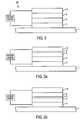
- FIG. 1illustrates a cross-sectional view of a chalcogenide glass constant current device fabricated in accordance with a first embodiment of the invention.
- FIG. 1 aillustrates a cross-sectional view of a chalcogenide glass constant current device fabricated in accordance with a first exemplary embodiment of the first embodiment of the invention.
- FIG. 1 billustrates a cross-sectional view of a chalcogenide glass constant current device fabricated in accordance with a second exemplary embodiment of the first embodiment of the invention.
- FIG. 1 cillustrates a cross-sectional view of a chalcogenide glass constant current device fabricated in accordance with a third exemplary embodiment of the first embodiment of the invention.
- FIG. 1 dillustrates a cross-sectional view of a chalcogenide glass constant current device fabricated in accordance with yet another exemplary embodiment of the first embodiment of the invention
- FIG. 2illustrates a cross-sectional view of a chalcogenide glass constant current device fabricated in accordance with a second embodiment of the invention.
- FIG. 2 aillustrates a cross-sectional view of a chalcogenide glass constant current device fabricated in accordance with a first exemplary embodiment of the second embodiment of the invention.
- FIG. 2 billustrates a cross-sectional view of a chalcogenide glass constant current device fabricated in accordance with a second exemplary embodiment of the second embodiment of the invention.
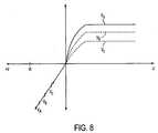
- FIG. 3is a graph illustrating a current-voltage (I-V) curve of a chalcogenide constant current device constructed in accordance with the invention.
- FIG. 4is a graph illustrating the application of different positive voltages to decrease a constant current device's constant current amplitude.
- FIG. 5is a graph illustrating the constant current achieved as a result of applying the voltage illustrated in FIG. 4 to a chalcogenide constant current device.
- FIG. 6is a graph illustrating the breakdown voltage of a chalcogenide constant current device.
- FIG. 7is a graph illustrating the I-V characteristics of a chalcogenide constant current device after a bias voltage described with reference to FIGS. 5-6 is applied.
- FIG. 8is a graph illustrating the original positive voltages applied to a chalcogenide constant current device and the resulting constant current I-V characteristics.
- FIG. 9illustrates a computer system incorporating a chalcogenide constant current device formed in accordance with the invention.
- substrateused in the following description may include any supporting structure including but not limited to a glass, plastic, or semiconductor substrate that has an exposed substrate surface.
- a semiconductor substrateshould be understood to include silicon, silicon-on-insulator (SOI), silicon-on-sapphire (SOS), doped and undoped semiconductors, epitaxial layers of silicon supported by a base semiconductor foundation, and other semiconductor structures which may not be silicon-based.
- SOIsilicon-on-insulator
- SOSsilicon-on-sapphire
- doped and undoped semiconductorssilicon-on-insulator
- epitaxial layers of silicon supported by a base semiconductor foundationand other semiconductor structures which may not be silicon-based.
- silveris intended to include not only elemental silver, but silver with other trace metals or in various alloyed combinations with other metals as is known in the semiconductor industry, as long as such silver alloy is conductive, and as long as the physical and electrical properties of the silver remain unchanged.
- silver-selenideis intended to include various species of silver-selenide, including some species which may have a slight excess or deficit of silver, for instance, Ag 2 Se, Ag 2+x Se, and Ag 2 ⁇ x Se.
- chalcogenide glassis intended to include glasses that comprise an element from group VIA (or group 16 ) of the periodic table.
- Group VIA elementsalso referred to as chalcogens, include sulfur (S), selenium (Se), tellurium (Te), polonium (Po), and oxygen (O).
- the present inventionis directed toward chalcogenide glass constant current devices and their methods of formation and operation.
- the chalcogenide constant current structures disclosed hereincan be utilized for any number of applications where a constant current is needed over a range of applied voltages.
- FIGS. 1-9illustrate exemplary embodiments of a chalcogenide constant current device 100 and 101 , and its method of formation and operation, in accordance with the invention.
- FIG. 1depicts a first embodiment of a chalcogenide constant current device constructed in accordance with the invention.
- a first electrode 2is formed over a substrate 1 .
- the first electrode 2may comprise any conductive material so long as the constant current device's electrical properties are not altered.
- various metalssuch as, one or more of tungsten, nickel, tantalum, aluminum, platinum, or titanium nitride among many others.
- the first electrode 2can comprise a conductively-doped semiconductive material.
- caremust be used since some metals, such as Ag, Au, or Cu, may migrate into a subsequently deposited glass layer and alter the electrical behavior of the constant current device.
- the first electrode 2is described as comprising tungsten (W).
- FIG. 1illustrates a first electrode 2 provided on substrate 1 , it should be appreciated that additional layers may be provided beneath electrode 2 , between it and the substrate 1 .
- a semiconductor substrate containing circuit layers covered with an insulating layercan be provided below first electrode 2 if desired. The presence of additional underlying layers between electrode 2 and substrate 1 does not affect the utility of the invention.
- a first chalcogenide glass layer 4is formed over the first conductive electrode 2 .
- the chalcogenide glass layer 4is electrically coupled to electrode 2 .
- the first chalcogenide glass layer 4is preferably a germanium-selenide glass having a Ge x Se 100-x stoichiometry.
- the stoichiometric range for the first chalcogenide glass layer 4is from about Ge 18 Se 82 to about Ge 43 Se 17 , but is preferably from about Ge 25 Se 75 to about Ge 40 Se 60 , and is more preferably about Ge 40 Se 60 .
- the first chalcogenide glass layer 4has a thickness that ranges from about 150 Angstroms ( ⁇ ) to about 400 ⁇ . Preferably, the first chalcogenide glass layer 4 has a thickness of about 250 ⁇ to about 300 ⁇ . For purposes of a simplified description, the first chalcogenide glass layer 4 is described further below as a Ge 40 Se 60 layer.
- the first chalcogenide glass layer 4acts as a glass backbone and allows a metal-containing layer, such as a silver-selenide or a chalcogenide-doped with silver (Ag) layer, to be directly formed thereon.
- the formation of the first chalcogenide glass layer 4having a stoichiometric composition, such as Ge 40 Se 60 in accordance with one exemplary embodiment of the invention, can be accomplished by any suitable method. For instance, evaporation, co-sputtering germanium and selenium in the appropriate ratios, sputtering using a germanium-selenide target having the desired stoichiometry, or chemical vapor deposition with stoichiometric amounts of GeH 4 and SeH 2 gases (or various compositions of these gases), which result in a germanium-selenide film of the desired stoichiometry, are non-limiting examples of methods which can be used to form the first chalcogenide glass layer 4 .
- a metal-containing layer 6preferably a silver-selenide layer, is formed over the first chalcogenide glass layer 4 .
- any suitable metal-containing layer 6may be used so long as it contains an adequate source of metal ions, which can move in and out of chalcogenide glass layers during device operation.
- the metal-containing layer 6may be silver.
- Other suitable metal-containing layers 6include all chalcogenide layers doped Ag such as chalcogenides O, S, Se, Te, and Po.
- Silver sulfide, silver oxide, and silver tellurideare all suitable silver-chalcogenides that may be used as metal-containing layer 6 .
- a variety of processescan be used to form the metal-containing layer 6 .
- Some non-limiting examplesare physical vapor deposition techniques such as evaporative deposition, sputtering, co-sputtering, starting with an Ag containing chalcogenide source.
- Other non-limiting processessuch as chemical vapor deposition, co-evaporation, depositing a layer of selenium above a layer of silver to form silver-selenide, or chemical bath deposition of a silver-selenide layer can also be used.
- the metal-containing layer 6is in contact with the upper surface of the first chalcogenide glass layer 4 ; however, intervening layers may also be provided between layers 4 and 6 , as long as they permit the resulting device to operate in a constant current mode.
- Metal-containing layer 6is formed to a thickness that ranges from about 200 ⁇ to about 2000 ⁇ . Preferably, the metal-containing layer 6 is about 600 ⁇ thick.
- FIG. 1illustrates that the second chalcogenide glass layer 8 is in contact with the upper surface of the metal-containing layer 6 ; however, intervening layers may also be provided between layers 6 and 8 , so long as they permit the resulting device to operate in a constant current mode.
- the second chalcogenide glass layer 8is preferably a germanium-selenide glass having a Ge x Se 100-x stoichiometry.
- the stoichiometric range for the second chalcogenide glass layer 8is from about Ge 18 Se 82 to about Ge 43 Se 57 , preferably from about Ge 25 Se 75 to about Ge 40 Se 60 , and is more preferably about Ge 40 Se 60 .
- the second chalcogenide glass layer 8preferably has a thickness that ranges from about 50 ⁇ to about 500 ⁇ . More preferably, the second chalcogenide glass layer 8 is about 150 ⁇ thick.
- first chalcogenide glass layer 4 and second chalcogenide glass layer 8are described-above as having a stoichiometry similar to each other, e.g., about Ge 40 Se 60 , it should be appreciated that the first chalcogenide glass layer 4 and the second chalcogenide glass layer 8 can possess different stoichiometries from each other, and they can even be different glasses.
- the first chalcogenide glass layer 4can possess a stoichiometry of Ge 40 Se 60 while the second chalcogenide glass layer 8 can possess a stoichiometry of Ge 25 Se 75 .
- the second chalcogenide glass layer 8is described further below as having a stoichiometry of Ge 40 Se 60 .
- the formation of the second chalcogenide glass layer 8can be accomplished by any suitable method as described above with reference to formation of the first chalcogenide glass layer 4 .
- an additional layer 9such as Ag can be provided above the second chalcogenide glass layer 8 .
- layer 9can be provided above (FIG. 1 b ) or below (FIG. 1 c ) metal-containing layer 6 , e.g., Ag 2 Se, rather than above the second chalcogenide glass layer 8 (FIG. 1 a ).
- layer 9is preferably an Ag layer that is less than or equal to about 500 ⁇ thick, and more preferably is an Ag layer that is approximately 200 ⁇ thick.
- Layer 9can be deposited using any techniques well-known in the art. It is not ideal to have an Ag source provided strictly by electrode 10 . Accordingly, care must be taken to limit the Ag source for long-term temperature stability and endurance. The presence of layer 9 addresses this concern. However, the presence of layer 9 is not required.
- a constant current devicecan be fabricated where a third glass layer 7 , analogous to glass layer 8 , can be provided between layer 9 and the top electrode 10 .
- layer 9is preferably an Ag layer that is less than or equal to about 500 ⁇ thick, and more preferably is an Ag layer that is approximately 200 ⁇ thick.
- a second electrode 10is formed over the second chalcogenide glass layer 8 , to complete the formation of the chalcogenide constant current device 100 .
- the second electrode 10may comprise any conductive material so long as the constant current device's electrical properties are not altered.
- various metalssuch as, one or more of tungsten, nickel, tantalum, aluminum, platinum, silver, or titanium nitride among many others.
- caremust be used since some metals, such as Ag, Au, or Cu, may migrate into a subsequently deposited glass layer and alter the electrical behavior of the constant current device.
- the second electrode 10can comprise a conductively-doped semiconductive material.
- FIG. 1illustrates that the second electrode 10 is in contact with an upper surface of the second chalcogenide glass layer 8 ; however, intervening layers may also be provided between layers 8 and 10 , as long as they permit the resulting device to operate in a constant current mode.
- first electrode 2 and the second electrode 10can comprise the same material or different materials.
- the first electrode 2 and second electrode 10can each be made of tungsten, or preferably, the first electrode 2 can comprise tungsten and the second electrode 10 can comprise silver.
- a negative electrical pulse of absolute amplitude greater than the erase potential of the deviceis applied to structure 100 in order to have the device exhibit constant current behavior.
- a structure 100 fabricated as shown in FIG. 1can be operated as a normal PCRAM memory device.
- the device 100can be read when a potential of approximately 100 mV is applied across conductors 10 and 2 , a voltage of approximately 250 mV or greater is applied across conductors 10 and 2 to write it, and a negative potential of absolute amplitude greater than approximately negative 80 mV is applied to conductors 10 and 2 to erase it.
- Applicantshave discovered that when a negative electrical pulse that is significantly more negative than the erase potential is applied across conductors 10 and 2 , the structure's electrical behavior is altered and it exhibits constant current source behavior rather than memory behavior.
- a wide range of negative voltagescan be applied across such a device without changing the device's current flow.
- the amplitude of the negative pulse signal that switches a device into constant current modee.g., significantly more negative than the PCRAM device's erase potential, will vary depending upon the thickness of the respective chalcogenide glass layers and the amount of metal, e.g., silver (Ag) present in the chalcogenide layer 4 .
- a first exemplary structure 100was formed in accordance with the FIG. 1 embodiment of the invention in which the first electrode 2 comprised tungsten, the first chalcogenide glass layer 4 comprised a Ge 40 Se 60 layer about 300 ⁇ thick, the metal-containing layer 6 comprised an Ag 2 Se layer about 600 ⁇ thick, the second chalcogenide glass layer 8 comprised a Ge 40 Se 60 layer about 150 ⁇ thick, and the second electrode 10 comprised an Ag electrode.
- the exemplary structure 100When a negative voltage typically within the range from about negative 1.0 V ( ⁇ 1.0 V) to about negative 2.0 V ( ⁇ 2.0 V), with a pulse of about 8 ns to at least about 30 ns, was applied across electrodes 10 and 2 , the exemplary structure 100 operated as a constant current device.
- a device fabricated in this mannerprovided a constant current of about negative 8 ⁇ A across an applied voltage range of about negative 100 mV ( ⁇ 100 mV) to at least about negative 800 mV ( ⁇ 800 mV), as graphically shown in FIG. 3.
- the constant current behavior of the exemplary structure 100begins to deteriorate. It was also found that devices fabricated in this manner permanently converted from a memory device into a constant current operation device.
- FIG. 3illustrates a constant current of about negative 8 pA across a voltage range of about ⁇ 100 mV to about ⁇ 800 mV
- the exact constant current value and voltage rangewill depend upon the structural properties of the device, such as the precise composition and thickness of layers 4 , 6 , and 8 , and the total amount of metal, e.g., silver, present in the chalcogenide layer 4 .
- first chalcogenide layer 4 and second chalcogenide layer 8do not have to possess the same stoichiometries, nor do the first chalcogenide layer 4 and second chalcogenide layer 8 have to possess the same thickness.
- a constant current device 100 fabricated as described with reference to FIG. 1can be of any geometric shape as desired or needed for a particular application.
- a constant current devicewas fabricated in accordance with a FIG. 1 embodiment of the invention in which the first electrode 2 comprised tungsten, the first chalcogenide layer 4 comprised a Ge 40 Se 60 glass about 300 ⁇ thick, the metal-containing layer 6 comprised an Ag 2 Se layer about 600 ⁇ thick, the second glass layer 8 comprised a Ge 25 Se 75 glass about 150 ⁇ thick, and the second electrode 10 comprised tungsten.
- the second exemplary structure 100maintained a constant current over an applied negative voltage range of about ⁇ 100 mV to about ⁇ 800 mV. Accordingly, the constant current observable voltage range was at least approximately 700 mV once a negative electrical 30 ns pulse in the range of about ⁇ 1.0 V to about ⁇ 2.0 V was applied across conductors 10 and 2 .
- a structure 100was fabricated including a first electrode 2 comprising tungsten, a layer 4 comprising Ge 40 Se 60 glass about 150 ⁇ thick, a metal-containing layer 6 comprising Ag 2 Se about 600 ⁇ thick, a glass layer 8 comprising Ge 40 Se 60 glass about 150 ⁇ thick, and a second electrode 10 comprising silver.
- a negative 8 ns electrical pulse of about negative 800 mV ( ⁇ 800 mV)was then applied to the fabricated device.
- this devicealso exhibited constant current behavior rather than memory behavior.
- the fabricated devicemaintained a constant current over an applied negative voltage range of at least approximately 700 mV, specifically from about ⁇ 100 mV to about ⁇ 800 mV, after a negative 8 ns electrical pulse of about ⁇ 800 mV was applied across electrodes 10 and 2 to convert the structure to a constant current mode.
- the total amount of silver present in the deviceseems to affect the magnitude of the negative potential that needs to be applied to switch a device 100 into constant current mode.
- FIG. 2shows another exemplary embodiment of the invention and its method of formation.
- the FIG. 2 embodimentillustrates a first electrode 2 provided over a substrate 1 .
- the first electrode 2may comprise any of the conductive materials listed above for the same electrode as in the FIG. 1 embodiment.
- the first electrode 2is described as tungsten (W). Similar to the FIG. 1 embodiment, additional layers may be provided between electrode 2 and substrate 1 .
- a chalcogenide glass layer 4is formed over the first electrode 2 .
- the chalcogenide glass layer 4is preferably a germanium-selenide glass having a Ge x Se 100-x stoichiometry.
- the stoichiometric range for the chalcogenide glass layer 4is from about Ge 18 Se 82 to about Ge 43 Se 57 , is preferably from about Ge 25 Se 75 to about Ge 40 Se 60 , and is more preferably about Ge 40 Se 60 .
- the chalcogenide glass layer 4has a thickness that ranges from about 150 ⁇ to about 400 ⁇ .
- the chalcogenide glass layer 4 in the FIG. 2 embodimenthas a thickness of about 250 ⁇ to about 300 ⁇ .
- the formation of the chalcogenide glass layer 4having a stoichiometric composition, such as Ge 40 Se 60 in accordance with one exemplary embodiment of the invention, can be accomplished by any of the methods described above for forming glass layers 4 or 8 of FIG. 1.
- a metal-containing layer 6preferably silver-selenide, is deposited over the chalcogenide glass layer 4 .
- any suitable metal-containing layer 6may be used so long as it contains an adequate source of metal ions, e.g., silver, which can move in and out of chalcogenide glass layer 4 during device operation.
- the metal-containing layer 6may be silver.
- Other suitable metal-containing layersinclude all chalcogenide layers containing Ag, e.g., chalcogenides O, S, Se, Te, and Po.
- Silver sulfide, silver oxide, and silver telluridefor example, among others, are all suitable silver-chalcogenides that may be used as metal-containing layer 6 , e.g., a chalcogenide layer containing Ag.
- Metal-containing layer 6can be formed by any of the methods described above in connection with forming metal-containing layer 6 of the FIG. 1 embodiment.
- FIG. 2illustrates that the metal-containing layer 6 is in contact with the upper surface of the chalcogenide glass layer 4 ; however, intervening layers may be present below metal-containing layer 6 so long as they do not prevent operation of the FIG. 2 structure in a constant current mode.
- Metal-containing layer 6is formed to a thickness that ranges from about 200 ⁇ to about 2000 ⁇ . Preferably, the metal-containing layer 6 is about 600 ⁇ thick.
- an additional layer 9such as Ag
- an additional layer 9can be provided above the metal-containing layer 6 , e.g., Ag 2 Se, between the second electrode 10 and the metal-containing layer 6 .
- an additional layer 9similar to the FIG. 2 a embodiment, can be provided below metal-containing layer 6 , between the first chalcogenide layer 4 and metal-containing layer 6 .
- layer 9is preferably an Ag layer that is less than or equal to 500 ⁇ thick, and more preferably an Ag layer that is approximately 200 ⁇ thick. Similar to the concerns for the exemplary FIG. 1 a - 1 d embodiments, care must be taken to limit the Ag source for long-term temperature stability and endurance. The presence of layer 9 addresses this concern. Again, the presence of layer 9 is not required.
- a second electrode 10is formed over the metal-containing layer 6 to complete the formation of the chalcogenide constant current device 101 , in accordance with the second embodiment.
- FIG. 2is described without intervening layers between the metal-containing layer 6 and the second electrode 10 , intervening layers may be present so long as they do not prevent operation of the FIG. 2 structure in a constant current mode.
- the second electrode 10may comprise any of the materials described above for electrode 10 in the FIG. 1 embodiment.
- the second electrode 10 of FIG. 2when the second electrode 10 of FIG. 2 is in direct contact with metal-containing layer 6 , the second electrode 10 should preferably not comprise silver unless it is sputtered onto an Ag 2 Se layer acting as metal-containing layer 6 .
- first electrode 2 and the second electrode 10 of FIG. 2can comprise the same material or different materials.
- first electrode 2 and second electrode 10can each be made of tungsten, or alternatively, the first electrode 2 can comprise tungsten and the second electrode 10 can comprise silver.
- a negative electrical potential of sufficient magnitudecan be applied across electrodes 10 and 2 to cause the device to exhibit constant current behavior.
- a device fabricated as shown in FIG. 2can be operated as a normal PCRAM memory device.
- the devicein DC operation, the device can be read when a potential of approximately 100 mV is applied across conductors 10 and 2 , a voltage of approximately 250 mV or greater is applied across conductors 10 and 2 to write it, and a negative potential of absolute amplitude greater than approximately negative 80 mV is applied to conductors 10 and 2 to erase it.
- a constant current devicewas fabricated in which the first electrode 2 comprised tungsten, the first layer 4 comprised a Ge 40 Se 60 glass about 300 ⁇ thick, the metal-containing layer 6 comprised an Ag 2 Se layer about 600 ⁇ thick, and the second electrode 10 comprised tungsten.
- a negative electrical 30 ns potential of 1.5 V ( ⁇ 1.5 V)was applied to the fabricated exemplary device. As a result, this device exhibited constant current behavior rather than memory behavior. It was further found that applying an electrical negative 30 ns potential that ranged from about ⁇ 1.0 V to about ⁇ 2.0 V to the fabricated device also generated constant current behavior. However, when a more positive electrical pulse than ⁇ 1.0 V was applied, for example, a negative 900 mV, 30 ns pulse, it was observed that this did not convert the exemplary device 101 into a constant current mode.
- the exemplary device 101maintained a constant current over an applied negative voltage range of about ⁇ 100 mV to about ⁇ 800 mV. Accordingly, the constant current observable voltage range is at least approximately 700 mV once a negative voltage in the range of about ⁇ 1.0 V to about ⁇ 2.0 V is applied across conductors 10 and 2 .
- a structure 101was fabricated including a first electrode 2 comprising tungsten, a layer 4 comprising Ge 40 Se 60 glass about 150 ⁇ thick, a metal-containing layer 6 comprising Ag 2 Se about 600 ⁇ thick, and a second electrode 10 comprising silver.
- a negative potential of 800 mV ( ⁇ 800 mV) with a 8 ns pulsewas applied to the fabricated device.
- this devicealso exhibited constant current behavior rather than memory behavior.
- the total amount of silver present in the device 101seems to affect the magnitude of the negative potential that needs to be applied to switch a device into constant current mode.
- the fabricated devicemaintained a constant current over an applied negative voltage range of at least approximately 700 mV, specifically from about ⁇ 100 mV to about ⁇ 800 mV, when a negative electrical potential of about ⁇ 800 mV was applied across electrodes 10 and 2 .
- the FIG. 2 embodimentcan be of any geometric shape depending upon the desired or needed application.
- devices 100 and 101 fabricated in accordance with the embodiments of the present inventionwhich normally exhibit PCRAM memory behavior, can be permanently converted to a constant current device by applying a negative voltage across the device in excess of the negative voltage required to switch the device from a memory device to a constant current device. Stated another way, applying a significantly more negative electrical pulse than the device's erase potential converts the memory device into a constant current device. It was also observed that the greater the amount of Ag present in the constant current devices 100 and 101 , a larger absolute amplitude, negative potential 8 ns pulse or a pulse of larger absolute amplitude at various widths could also be applied to devices 100 and 101 to induce constant current behavior.
- devices 100 and 101 fabricated in accordance with the inventioncan be operated as a constant current device without first operating as a memory device, upon application of a negative electrical pulse sufficient to place the device in a constant current mode of operation.
- devices 100 and 101 fabricated in accordance with the inventionmay be operated as a memory device without first operating then as a constant current device by application of voltages below the threshold required to place the device in a constant current mode.
- the deviceupon application of a negative pulse sufficient to place the memory device in a constant current mode of operation, the device converts to a constant current mode and remains in that state even when voltage is removed.
- the inventionprovides methods for changing and resetting the current level which passes through constant current devices 100 and 101 such as described in FIGS. 1 and 2, when in a constant current operation mode.
- an exemplary structure 100 formed in accordance with FIG. 1is described below in reference to FIG. 3, comprises a bottom tungsten electrode 2 , a Ge 40 Se 60 first glass layer 4 about 300 ⁇ thick, a Ag 2 Se layer 6 about 600 ⁇ thick, a Ge 40 Se 60 second glass layer 8 about 150 ⁇ thick, and a top silver electrode 10 .
- the structure 100 of FIG. 1is in a constant current mode and a DC voltage in the range of approximately 0 to approximately ⁇ 1.0 V is applied across electrodes 10 and 2 , the device has the current/voltage curve (I/V curve) as illustrated in FIG. 3.
- FIG. 3illustrates an observed region A beyond about ⁇ 800 mV where the constant current value of ⁇ 8 ⁇ A begins to decline for the constant current devices of the invention. Stated in another way, region A is where the constant current value is no longer maintained at ⁇ 8 ⁇ A. It has been observed that Region A corresponds to a reset region or breakdown area of a chalcogenide constant current device 100 . Specifically, when structure 100 is in constant current operation mode, as depicted in FIG. 3, the constant current value of the device can be reset to its initial constant current value, for example ⁇ 8 ⁇ A, by applying a more negative voltage greater than the negative voltage threshold of the device. The initial constant current value is the initial current value of the chalcogenide structure when it is first switched to exhibit constant current behavior.
- a constant current devicecan prematurely degrade if the applied potential is increased too much above the point where the constant current device starts to reduce the constant current value as illustrated in FIG. 3.
- the degradation of the constant current devicecan eventually lead to DNR behavior.
- the increase in the constant current's valuecan occur with a repeated pulse of similar or less amplitude as initially used to cause the device to exhibit constant current behavior.
- a constant current devicewill not reset to its initial constant current value.
- the constant current device's functionis killed.
- a more preferable method of resetting a constant current device's constant current valueis applying a more positive electrical potential.
- the constant current levelis depicted as ⁇ 8 ⁇ A
- the constant current valuewill vary depending upon the thickness of the glass stack fabricated in accordance with the embodiments of FIGS. 1 and 2, and also depending upon the total amount of Ag in devices 100 and 101 .
- region Ais observed beyond about ⁇ 800 mV in FIG. 3, region A's location can also vary, e.g., be greater or less than the value depicted in FIG. 3, depending upon the thickness of the glass stack, total amount of silver, and applied negative voltage.
- the devicemaintains a constant current of at least 700 mV, the thickness of the glass stack, total amount of silver, and magnitude of the applied negative voltage, will also affect the device's range for maintaining a constant current value, e.g., a constant current device can possess a greater constant current range than depicted.
- region A of FIG. 3corresponds to a negative breakdown voltage which can be applied to a constant current structure 100 or 101 to reset the structure's constant current value to the original value observed when structures 100 or 101 was initially switched to constant current mode.
- FIG. 3also illustrates a method for changing the constant current value of device 100 .
- Applicantshave discovered that applying a negative potential, up to a certain value increases the constant current's amplitude. Repeated current pulses of similar or less amplitude can further increase the constant current's amplitude. The negative potential necessary to increase the constant current's amplitude will vary depending upon the structural characteristics of the constant current device Conversely, applying a positive potential decreases the constant current's amplitude. Similarly, repeated current pulses of similar or less amplitude can further decrease the constant current's amplitude. Again, the positive potential necessary to decrease the constant current's amplitude will vary depending on the structural characteristics of the constant current device. Further details are provided below.
- FIG. 5illustrates a constant current limit 61 , after a positive voltage 60 , e.g., V 1 is applied to structure 100 that is larger than the Vt shown in FIG. 4.
- FIG. 4illustrates, the magnitude of V 1 's which can be applied to constant current structure 100 can be of a larger absolute amplitude than positive Vt voltage 60 .
- graph 61corresponds to the applied positive Vt voltage 60 of FIG. 4
- graph 71corresponds to the applied positive voltage 70 of FIG. 4
- graph 81corresponds to the applied positive voltage 80 of FIG. 4.
- FIG. 4illustrates only a small number of V 1 's that can be applied to induce a larger constant current value, e.g., decreasing the constant current's amplitude.
- FIG. 5illustrates only a small number of V 1 's that can be applied to induce a larger constant current value, e.g., decreasing the constant current's amplitude.
- FIG. 5illustrates only a small number of constant current values that can result from an applied positive voltage to structure 100 operating in constant current mode. Further, FIG. 5 illustrates that repeated current pulses of similar or less amplitude can further decrease the constant current's amplitude as graphs 61 , 71 , and 81 illustrate.
- a positive voltagee.g., V 1
- Vta positive voltage
- a positive voltage 70can be applied to achieve a new constant current value illustrated in FIG. 5, graph 71 .
- V 1is applied to the structure reducing the constant current strength.
- the constant current valuecan be continuously decreased if desired. Therefore, applying a positive voltage, e.g., V 1 , to constant current devices 100 and 101 allows one to change the constant current value to a lower constant current value than the device initially exhibited.
- the inventionprovides a method of increasing or resetting the high constant current value achieved with the methods described previously in reference to FIGS. 4 and 5.
- a voltage more negative than a negative threshold voltage (Vt)needs to be applied to structure 100 .
- This voltageis also known as the breakdown voltage of the device. For purposes of a simplified description, this voltage is described as V 2 .
- FIG. 6illustrates in region A (analogous to region A of FIG. 3), the breakdown voltage of a constant current device 100 utilizing the constant current limit graph 60 of FIG. 5.
- a negative threshold voltage (V 2 )is applied at a voltage slightly more negative than the upper voltage limit range for the existing constant current level, defined as the breakdown voltage of the device.
- FIG. 6illustrates that negative 800 mV ( ⁇ 800 mV) is about the upper voltage limit range for the existing constant current value of structure 100 . Therefore, a V 2 must be applied that is slightly more negative than ⁇ 800 mV as FIG. 6 illustrates. Specifically, the breakdown voltage of constant current device 100 is provided by Region A, which is slightly more negative than ⁇ 800 mV.
- FIG. 6illustrates applying V 2 which is more negative than about ⁇ 800 mV to constant current structure 100 .
- a more negative V 2 of equal to or greater than ⁇ 1.0 Vis applied to reset the constant current value of structure 100 .
- other negative V 2 valuescan be used so long as they are greater than the constant current value's upper voltage limit range of structure 100 , e.g., a V 2 greater than at least ⁇ 800 mV.
- FIG. 3illustrates that the constant current's upper voltage limit range is approximately ⁇ 800 mV for constant current structure 100 .
- a slightly more negative V 2is applied. This is illustrated by Region A.
- this negative signale.g., V 2
- V 2the exact breakdown voltage and the amplitude of this negative signal, e.g., V 2
- V 2the exact breakdown voltage and the amplitude of this negative signal
- applying a V 2 which corresponds to the breakdown voltage of the constant current deviceraises the existing constant current value, e.g., the existing constant current value becomes more negative or increases the constant current's amplitude.
- applying a more negative voltage that corresponds to region A of FIGS. 3 and 6,can either reset the constant current limit of structure 100 to the original constant current limit or at least raise the constant current value, e.g., make more negative, of the constant current device as FIG. 7 illustrates.
- repeated current pulses of similar or less amplitudecan further increase the constant current's amplitude as desired.
- FIG. 7illustrates that the constant current value of structure 100 is raised, e.g., from about ⁇ 8 ⁇ A as FIG. 6 illustrates, to about negative 800 nA ( ⁇ 800 nA).
- a new higher constant current valueis achieved, e.g., more negative constant current value.
- the higher constant current value achievedcorresponds to the original negative constant current value of the constant current device.
- the constant current valueis significantly higher, e.g., more negative.
- a breakdown voltage within region A(which will vary as described above for each constant current device) that ranges from about ⁇ 800 mV to about ⁇ 2.0 V be applied to a constant current device such as devices 100 and 101 to reset or raise their constant current values, e.g., make more negative.
- a more negative V 2 greater than ⁇ 2.0 Vtypically results in the constant current device being destroyed, this is not always the case.
- This value e.g., ⁇ 2.0 Vmay vary depending upon the thickness of the layers within the constant current device. For instance, the thicker the device, a more negative V 2 may be applied e.g., more negative than ⁇ 2.0 V without destroying the device. Further, applying a more negative V 2 greater than ⁇ 2.0 V may result in the device resetting to a very low constant current value at which point the device can be pulsed and programmed as a constant current source again rather than destroying the device. Again, this is dependent on the thickness of the layers present in the constant current device. Thus, in one aspect, applying a more negative V 2 greater than ⁇ 2.0 V can result in the device resetting to a low constant current value.
- the methods disclosed aboveallow a constant current device's constant current level to be changed and reset. Changing or resetting the constant current value is non-destructive to the chalcogenide constant current device 100 or 101 . Therefore, the constant current limit's value can be decreased, e.g., made more positive than the original constant current level of the constant current device by applying a V 1 voltage, and conversely, the constant current level can be reset or raised, e.g., made more negative than the original constant current value. It should be appreciated that the methods of the present invention are applicable to any constant current device and not limited to devices 100 and 101 constructed in accordance with FIGS. 1 and 2.
- the inventionalso provides a method of utilizing a constant current device such that it functions as an analog memory device.
- This specific aspectprovides a method of examining the constant current values which were applied to a constant current device. Once these constant current values are determined, the positive voltages, e.g., V 1 , that were applied to achieve the constant current values can also be determined. In turn, these values can be read such that a memory state can correspond to each constant current value.
- the constant current devicecan be read such that a plurality of memory states can be stored. Each memory state corresponds to a specific constant current value. For instance, repeated current pulses of similar or less amplitude can further increase or decrease the constant current's amplitude. Each of these values can be read and stored for an analog assortment of varying states.
- FIG. 8illustrates the method for reading the constant current values of a constant current device such that it functions as an analog memory device.
- a constant current devicesuch that it functions as an analog memory device.
- V 1a positive voltage
- FIG. 4illustrates
- FIG. 4the constant current device decreases the value of the constant current limit, e.g., makes the constant current amplitude decrease
- FIG. 5illustrates.
- Applying a positive voltage such as lines 60 , 70 , and 80 of FIG. 4can result in lines 61 , 71 , and 81 of FIG. 5. At least one of these constant current values can be stored and read individually.
- a plurality of constant current valuescan be achieved in a single constant current device.
- FIG. 8graphically illustrates V a , V b , and V c .
- the positive voltage which was applied to achieve V a , V b , and V ccan be determined.
- the constant current value V aallows the calculation of the positive V 1 that was applied to cause V a .
- utilizing the constant current values of V b and V callows the calculation of the positive V 1 that was applied to cause V b and V c .
- Each corresponding constant current value, V a , V b , and V cfor instance, can then be stored as a separate memory state for the device.
- the embodiments described aboverefer to the formation of only one chalcogenide constant current structure 100 or 101 , it must be understood that the invention contemplates the formation of any number of such chalcogenide constant current structures.
- a plurality of chalcogenide constant current structurescan be fabricated and provided and operated with a plurality of elements as a non-limiting example.
- the chalcogenide glass constant current structure 100 or 101can be utilized in many electronic devices.
- the methods and operation of the structures disclosed abovecan be used in any device whenever it is desired to have a constant current maintaining device that maintains a constant current over a wide range of applied voltages.
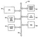
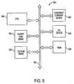
- a typical processor based system which includes a constant current device according to the present inventionis illustrated generally at 500 in FIG. 9.
- a processor based systemis exemplary of a system having digital circuits which could include constant current devices. Without being limiting, such a system could include a computer system, camera system, scanner, machine vision, vehicle navigation, video phone, surveillance system, auto focus system, star tracker system, motion detection system, image stabilization system and data compression system for high-definition television, all of which can utilize the present invention.
- a processor based systemsuch as a computer system, for example generally comprises a central processing unit (CPU) 544 , for example, a microprocessor, that communicates with an input/output (I/O) device 546 over a bus 552 .
- the constant current device 542also communicates with the system over bus 552 .
- the computer system 500also includes random access memory (RAM) 548 , and, in the case of a computer system may include peripheral devices such as a floppy disk drive 554 and a compact disk (CD) ROM drive 556 which also communicate with CPU 544 over the bus 552 .
- RAMrandom access memory
- Constant current device 542is preferably constructed as an integrated circuit containing at least one chalcogenide glass layer and a metal-containing layer, as previously described with respect to FIGS. 1-8. It may also be desirable to integrate the processor 554 , constant current device 542 and memory 548 on a single IC chip.
Landscapes
- Chemical & Material Sciences (AREA)
- Engineering & Computer Science (AREA)
- Chemical Kinetics & Catalysis (AREA)
- General Chemical & Material Sciences (AREA)
- Materials Engineering (AREA)
- Organic Chemistry (AREA)
- Life Sciences & Earth Sciences (AREA)
- Geochemistry & Mineralogy (AREA)
- Manufacturing & Machinery (AREA)
- Inorganic Chemistry (AREA)
- Mechanical Engineering (AREA)
- Metallurgy (AREA)
- Crystallography & Structural Chemistry (AREA)
- Semiconductor Memories (AREA)
- Lasers (AREA)
- Control Of Electrical Variables (AREA)
Abstract
Description
- The present invention relates to a constant current device, and more specifically, to a constant current device formed of chalcogenide materials.[0001]
- Programmable resistive materials based on chalcogenide glass are being explored for use as non-volatile memory elements. By applying an external stimulus, such as different voltages of selected polarities to a chalcogenide glass in the presence of an available metal such as silver, the internal structure of the chalcogenide glass can be modified to produce high or low resistance states.[0002]
- One specific example of a chalcogenide glass being investigated for memory use is germanium-selenide (Ge[0003]xSe100-x). Typically, the chalcogenide glass has an associated layer for supplying a metal, which becomes incorporated with the glass matrix to change resistance states. As examples, the associated layer may be a layer of silver or a layer of silver-selenide (Ag2Se).
- While the current focus is on using chalcogenide glass for memory devices, the inventors have discovered another use for chalcogenide glass, namely, as a constant current device.[0004]
- In one aspect, the invention provides a two-terminal constant current device formed of a chalcogenide glass material, and its method of formation and operation. The device comprises a metal-containing layer formed adjacent at least one chalcogenide glass layer which is biased into a constant current state. The constant current device maintains a constant current over a range of applied voltages.[0005]
- In another aspect, the invention provides a constant current device and a method of forming and operating such a device in which at least one layer of silver-selenide is formed between a first germanium-selenide layer and a second germanium-selenide layer. These layers are provided between a first and a second electrode. A bias voltage is applied to the electrodes sufficient to place the device in a constant current state. The constant current device maintains a constant current over a range of applied voltages.[0006]
- In another aspect, the invention provides a constant current device and a method of forming and operating such a device in which at least one layer of silver-selenide is formed between a first germanium-selenide layer, a layer of silver, and a second germanium-selenide layer. These layers are provided between a first and a second electrode. A bias voltage is applied to the electrodes sufficient to place the device in a constant current state. The constant current device maintains a constant current over a range of applied voltages.[0007]
- In another aspect, the invention provides a constant current device and a method of forming and operating such a device in which at least one metal-containing layer, such as silver, is formed on a chalcogenide glass layer such as a germanium-selenide layer. A bias voltage is applied to the layers sufficient to place the device in a constant current state. The constant current device maintains a constant current over a range of applied voltages.[0008]
- In another aspect, the invention provides a constant current device and a method of forming and operating such a device in which at least one metal-containing layer, such as silver-selenide, is formed with a chalcogenide glass layer such as a germanium-selenide layer, and a layer of silver. A bias voltage is applied to these layers sufficient to place the device in a constant current state. The constant current device maintains a constant current over a range of applied voltages.[0009]
- In another aspect, the invention provides a method of converting a device that has been exhibiting memory behavior comprised of at least one chalcogenide glass layer and a metal-containing layer, for example, of silver or silver-selenide to a constant current device. A bias voltage is applied to the layers sufficient to place the device in a constant current state. The constant current device maintains a constant current over a range of applied voltages.[0010]
- In another aspect, the invention provides a method of altering the current characteristics of a constant current device formed with at least one chalcogenide glass layer by manipulation of an applied bias voltage.[0011]
- In another aspect, the invention provides a method of resetting or raising the current characteristics of a constant current device formed with at least one chalcogenide glass layer to a prior state by manipulation of an applied bias voltage.[0012]
- These and other features and advantages of the invention will be better understood from the following detailed description, which is provided in connection with the accompanying drawings.[0013]
- FIG. 1 illustrates a cross-sectional view of a chalcogenide glass constant current device fabricated in accordance with a first embodiment of the invention.[0014]
- FIG. 1[0015]aillustrates a cross-sectional view of a chalcogenide glass constant current device fabricated in accordance with a first exemplary embodiment of the first embodiment of the invention.
- FIG. 1[0016]billustrates a cross-sectional view of a chalcogenide glass constant current device fabricated in accordance with a second exemplary embodiment of the first embodiment of the invention.
- FIG. 1[0017]cillustrates a cross-sectional view of a chalcogenide glass constant current device fabricated in accordance with a third exemplary embodiment of the first embodiment of the invention.
- FIG. 1[0018]dillustrates a cross-sectional view of a chalcogenide glass constant current device fabricated in accordance with yet another exemplary embodiment of the first embodiment of the invention
- FIG. 2 illustrates a cross-sectional view of a chalcogenide glass constant current device fabricated in accordance with a second embodiment of the invention.[0019]
- FIG. 2[0020]aillustrates a cross-sectional view of a chalcogenide glass constant current device fabricated in accordance with a first exemplary embodiment of the second embodiment of the invention.
- FIG. 2[0021]billustrates a cross-sectional view of a chalcogenide glass constant current device fabricated in accordance with a second exemplary embodiment of the second embodiment of the invention.
- FIG. 3 is a graph illustrating a current-voltage (I-V) curve of a chalcogenide constant current device constructed in accordance with the invention.[0022]
- FIG. 4 is a graph illustrating the application of different positive voltages to decrease a constant current device's constant current amplitude.[0023]
- FIG. 5 is a graph illustrating the constant current achieved as a result of applying the voltage illustrated in FIG. 4 to a chalcogenide constant current device.[0024]
- FIG. 6 is a graph illustrating the breakdown voltage of a chalcogenide constant current device.[0025]
- FIG. 7 is a graph illustrating the I-V characteristics of a chalcogenide constant current device after a bias voltage described with reference to FIGS. 5-6 is applied.[0026]
- FIG. 8 is a graph illustrating the original positive voltages applied to a chalcogenide constant current device and the resulting constant current I-V characteristics.[0027]
- FIG. 9 illustrates a computer system incorporating a chalcogenide constant current device formed in accordance with the invention.[0028]
- In the following detailed description, reference is made to various specific embodiments of the invention. These embodiments are described with sufficient detail to enable those skilled in the art to practice the invention. It is to be understood that other embodiments may be employed, and that various structural, logical, and electrical changes may be made without departing from the spirit or scope of the invention.[0029]
- The term “substrate” used in the following description may include any supporting structure including but not limited to a glass, plastic, or semiconductor substrate that has an exposed substrate surface. A semiconductor substrate should be understood to include silicon, silicon-on-insulator (SOI), silicon-on-sapphire (SOS), doped and undoped semiconductors, epitaxial layers of silicon supported by a base semiconductor foundation, and other semiconductor structures which may not be silicon-based. When reference is made to a semiconductor substrate in the following description, previous process steps may have been utilized to form regions or junctions in and/or over the base semiconductor or foundation.[0030]
- The term “silver” is intended to include not only elemental silver, but silver with other trace metals or in various alloyed combinations with other metals as is known in the semiconductor industry, as long as such silver alloy is conductive, and as long as the physical and electrical properties of the silver remain unchanged.[0031]
- The term “silver-selenide” is intended to include various species of silver-selenide, including some species which may have a slight excess or deficit of silver, for instance, Ag[0032]2Se, Ag2+xSe, and Ag2−xSe.
- The term “chalcogenide glass” is intended to include glasses that comprise an element from group VIA (or group[0033]16) of the periodic table. Group VIA elements, also referred to as chalcogens, include sulfur (S), selenium (Se), tellurium (Te), polonium (Po), and oxygen (O).
- The present invention is directed toward chalcogenide glass constant current devices and their methods of formation and operation. The chalcogenide constant current structures disclosed herein can be utilized for any number of applications where a constant current is needed over a range of applied voltages.[0034]
- The invention will now be explained with reference to FIGS. 1-9, which illustrate exemplary embodiments of a chalcogenide constant[0035]
current device - FIG. 1 depicts a first embodiment of a chalcogenide constant current device constructed in accordance with the invention. A[0036]
first electrode 2 is formed over asubstrate 1. Thefirst electrode 2 may comprise any conductive material so long as the constant current device's electrical properties are not altered. For example, various metals, such as, one or more of tungsten, nickel, tantalum, aluminum, platinum, or titanium nitride among many others. In addition, thefirst electrode 2 can comprise a conductively-doped semiconductive material. However, care must be used since some metals, such as Ag, Au, or Cu, may migrate into a subsequently deposited glass layer and alter the electrical behavior of the constant current device. - For purposes of a simplified description, the[0037]
first electrode 2 is described as comprising tungsten (W). Although FIG. 1 illustrates afirst electrode 2 provided onsubstrate 1, it should be appreciated that additional layers may be provided beneathelectrode 2, between it and thesubstrate 1. For instance, a semiconductor substrate containing circuit layers covered with an insulating layer can be provided belowfirst electrode 2 if desired. The presence of additional underlying layers betweenelectrode 2 andsubstrate 1 does not affect the utility of the invention. - Next, a first[0038]
chalcogenide glass layer 4 is formed over the firstconductive electrode 2. Thechalcogenide glass layer 4 is electrically coupled toelectrode 2. - The first[0039]
chalcogenide glass layer 4 is preferably a germanium-selenide glass having a GexSe100-xstoichiometry. The stoichiometric range for the firstchalcogenide glass layer 4 is from about Ge18Se82to about Ge43Se17, but is preferably from about Ge25Se75to about Ge40Se60, and is more preferably about Ge40Se60. - The first[0040]
chalcogenide glass layer 4 has a thickness that ranges from about 150 Angstroms (Å) to about 400 Å. Preferably, the firstchalcogenide glass layer 4 has a thickness of about 250 Å to about 300 Å. For purposes of a simplified description, the firstchalcogenide glass layer 4 is described further below as a Ge40Se60layer. The firstchalcogenide glass layer 4 acts as a glass backbone and allows a metal-containing layer, such as a silver-selenide or a chalcogenide-doped with silver (Ag) layer, to be directly formed thereon. - The formation of the first[0041]
chalcogenide glass layer 4, having a stoichiometric composition, such as Ge40Se60in accordance with one exemplary embodiment of the invention, can be accomplished by any suitable method. For instance, evaporation, co-sputtering germanium and selenium in the appropriate ratios, sputtering using a germanium-selenide target having the desired stoichiometry, or chemical vapor deposition with stoichiometric amounts of GeH4and SeH2gases (or various compositions of these gases), which result in a germanium-selenide film of the desired stoichiometry, are non-limiting examples of methods which can be used to form the firstchalcogenide glass layer 4. - Still referring to FIG. 1, a metal-containing[0042]
layer 6, preferably a silver-selenide layer, is formed over the firstchalcogenide glass layer 4. However, any suitable metal-containinglayer 6 may be used so long as it contains an adequate source of metal ions, which can move in and out of chalcogenide glass layers during device operation. For instance, besides silver-selenide, the metal-containinglayer 6 may be silver. Other suitable metal-containinglayers 6 include all chalcogenide layers doped Ag such as chalcogenides O, S, Se, Te, and Po. Silver sulfide, silver oxide, and silver telluride, for example, among others, are all suitable silver-chalcogenides that may be used as metal-containinglayer 6. - A variety of processes can be used to form the metal-containing[0043]
layer 6. Some non-limiting examples are physical vapor deposition techniques such as evaporative deposition, sputtering, co-sputtering, starting with an Ag containing chalcogenide source. Other non-limiting processes such as chemical vapor deposition, co-evaporation, depositing a layer of selenium above a layer of silver to form silver-selenide, or chemical bath deposition of a silver-selenide layer can also be used. FIG. 1 illustrates that the metal-containinglayer 6 is in contact with the upper surface of the firstchalcogenide glass layer 4; however, intervening layers may also be provided betweenlayers - Metal-containing[0044]
layer 6 is formed to a thickness that ranges from about 200 Å to about 2000 Å. Preferably, the metal-containinglayer 6 is about 600 Å thick. - Still referring to FIG. 1, a second[0045]
chalcogenide glass layer 8 is formed over the metal-containinglayer 6. FIG. 1 illustrates that the secondchalcogenide glass layer 8 is in contact with the upper surface of the metal-containinglayer 6; however, intervening layers may also be provided betweenlayers - The second[0046]
chalcogenide glass layer 8 is preferably a germanium-selenide glass having a GexSe100-xstoichiometry. The stoichiometric range for the secondchalcogenide glass layer 8 is from about Ge18Se82to about Ge43Se57, preferably from about Ge25Se75to about Ge40Se60, and is more preferably about Ge40Se60. The secondchalcogenide glass layer 8 preferably has a thickness that ranges from about 50 Å to about 500 Å. More preferably, the secondchalcogenide glass layer 8 is about 150 Å thick. - Although the first[0047]
chalcogenide glass layer 4 and secondchalcogenide glass layer 8 are described-above as having a stoichiometry similar to each other, e.g., about Ge40Se60, it should be appreciated that the firstchalcogenide glass layer 4 and the secondchalcogenide glass layer 8 can possess different stoichiometries from each other, and they can even be different glasses. For instance, the firstchalcogenide glass layer 4 can possess a stoichiometry of Ge40Se60while the secondchalcogenide glass layer 8 can possess a stoichiometry of Ge25Se75. For purposes of a simplified description, the secondchalcogenide glass layer 8 is described further below as having a stoichiometry of Ge40Se60. - The formation of the second[0048]
chalcogenide glass layer 8, can be accomplished by any suitable method as described above with reference to formation of the firstchalcogenide glass layer 4. - As an alternative embodiment, depicted in FIG. 1[0049]a, an
additional layer 9, such as Ag, can be provided above the secondchalcogenide glass layer 8. Alternatively,layer 9 can be provided above (FIG. 1b) or below (FIG. 1c) metal-containinglayer 6, e.g., Ag2Se, rather than above the second chalcogenide glass layer8 (FIG. 1a). In FIGS. 1a-1c,layer 9 is preferably an Ag layer that is less than or equal to about 500 Å thick, and more preferably is an Ag layer that is approximately 200 Å thick.Layer 9 can be deposited using any techniques well-known in the art. It is not ideal to have an Ag source provided strictly byelectrode 10. Accordingly, care must be taken to limit the Ag source for long-term temperature stability and endurance. The presence oflayer 9 addresses this concern. However, the presence oflayer 9 is not required. - Further, in yet another alternative embodiment of FIG. 1, depicted in FIG. 1[0050]d, a constant current device can be fabricated where a third glass layer7, analogous to
glass layer 8, can be provided betweenlayer 9 and thetop electrode 10. Similar to the embodiments depicted in FIGS. 1a-1c,layer 9 is preferably an Ag layer that is less than or equal to about 500 Å thick, and more preferably is an Ag layer that is approximately 200 Å thick. - Referring back to FIG. 1, a[0051]
second electrode 10 is formed over the secondchalcogenide glass layer 8, to complete the formation of the chalcogenide constantcurrent device 100. Thesecond electrode 10 may comprise any conductive material so long as the constant current device's electrical properties are not altered. For example, various metals, such as, one or more of tungsten, nickel, tantalum, aluminum, platinum, silver, or titanium nitride among many others. However, care must be used since some metals, such as Ag, Au, or Cu, may migrate into a subsequently deposited glass layer and alter the electrical behavior of the constant current device. - In addition, the[0052]
second electrode 10 can comprise a conductively-doped semiconductive material. FIG. 1 illustrates that thesecond electrode 10 is in contact with an upper surface of the secondchalcogenide glass layer 8; however, intervening layers may also be provided betweenlayers - It should be appreciated that the[0053]
first electrode 2 and thesecond electrode 10 can comprise the same material or different materials. As examples, thefirst electrode 2 andsecond electrode 10 can each be made of tungsten, or preferably, thefirst electrode 2 can comprise tungsten and thesecond electrode 10 can comprise silver. As described previously, it is not ideal to have an Ag source provided strictly byelectrode 10. Accordingly, care must be taken to limit the Ag source for long-term temperature stability and endurance. - After forming the[0054]
second electrode 10, a negative electrical pulse of absolute amplitude greater than the erase potential of the device is applied to structure100 in order to have the device exhibit constant current behavior. Conventionally, astructure 100 fabricated as shown in FIG. 1, can be operated as a normal PCRAM memory device. For example, in DC operation, thedevice 100 can be read when a potential of approximately 100 mV is applied acrossconductors conductors conductors - However, Applicants have discovered that when a negative electrical pulse that is significantly more negative than the erase potential is applied across[0055]
conductors chalcogenide layer 4. - A first[0056]
exemplary structure 100 was formed in accordance with the FIG. 1 embodiment of the invention in which thefirst electrode 2 comprised tungsten, the firstchalcogenide glass layer 4 comprised a Ge40Se60layer about 300 Å thick, the metal-containinglayer 6 comprised an Ag2Se layer about 600 Å thick, the secondchalcogenide glass layer 8 comprised a Ge40Se60layer about 150 Å thick, and thesecond electrode 10 comprised an Ag electrode. - When a negative voltage typically within the range from about negative 1.0 V (−1.0 V) to about negative 2.0 V (−2.0 V), with a pulse of about 8 ns to at least about 30 ns, was applied across[0057]
electrodes exemplary structure 100 operated as a constant current device. A device fabricated in this manner provided a constant current of about negative 8 μA across an applied voltage range of about negative 100 mV (−100 mV) to at least about negative 800 mV (−800 mV), as graphically shown in FIG. 3. When the voltage becomes more negative than approximately −800 mV, the constant current behavior of theexemplary structure 100 begins to deteriorate. It was also found that devices fabricated in this manner permanently converted from a memory device into a constant current operation device. - Although FIG. 3 illustrates a constant current of about negative 8 pA across a voltage range of about −100 mV to about −800 mV, it should be appreciated that the exact constant current value and voltage range will depend upon the structural properties of the device, such as the precise composition and thickness of[0058]
layers chalcogenide layer 4. - Further, as noted above regarding the FIG. 1 embodiment, the[0059]
first chalcogenide layer 4 andsecond chalcogenide layer 8 do not have to possess the same stoichiometries, nor do thefirst chalcogenide layer 4 andsecond chalcogenide layer 8 have to possess the same thickness. A constantcurrent device 100 fabricated as described with reference to FIG. 1 can be of any geometric shape as desired or needed for a particular application. - As a second and more specific exemplary example, a constant current device was fabricated in accordance with a FIG. 1 embodiment of the invention in which the[0060]
first electrode 2 comprised tungsten, thefirst chalcogenide layer 4 comprised a Ge40Se60glass about 300 Å thick, the metal-containinglayer 6 comprised an Ag2Se layer about 600 Å thick, thesecond glass layer 8 comprised a Ge25Se75glass about 150 Å thick, and thesecond electrode 10 comprised tungsten. - When a negative potential of 1.5 V (−1.5 V) with a 30 ns pulse was applied to the fabricated device, the device exhibited constant current behavior rather than memory behavior. Applicants further learned that applying a negative potential anywhere in the voltage ranges from about −1.0 V to about −2.0 V with a 30 ns pulse to the fabricated device, also generated constant current behavior. However, it was found that applying a negative 900 mV, 30 ns pulse did not cause the fabricated device exhibit constant current behavior.[0061]
- Similar to the first exemplary device, the second[0062]
exemplary structure 100, maintained a constant current over an applied negative voltage range of about −100 mV to about −800 mV. Accordingly, the constant current observable voltage range was at least approximately 700 mV once a negative electrical 30 ns pulse in the range of about −1.0 V to about −2.0 V was applied acrossconductors - In a third exemplary example of the FIG. 1 embodiment, a[0063]
structure 100 was fabricated including afirst electrode 2 comprising tungsten, alayer 4 comprising Ge40Se60glass about 150 Å thick, a metal-containinglayer 6 comprising Ag2Se about 600 Å thick, aglass layer 8 comprising Ge40Se60glass about 150 Å thick, and asecond electrode 10 comprising silver. A negative 8 ns electrical pulse of about negative 800 mV (−800 mV) was then applied to the fabricated device. - As a result, this device also exhibited constant current behavior rather than memory behavior. The fabricated device maintained a constant current over an applied negative voltage range of at least approximately 700 mV, specifically from about −100 mV to about −800 mV, after a negative 8 ns electrical pulse of about −800 mV was applied across[0064]
electrodes device 100 into constant current mode. - Reference is now made to FIG. 2 which shows another exemplary embodiment of the invention and its method of formation.[0065]
- The FIG. 2 embodiment illustrates a[0066]
first electrode 2 provided over asubstrate 1. Thefirst electrode 2 may comprise any of the conductive materials listed above for the same electrode as in the FIG. 1 embodiment. For purposes of a simplified description, thefirst electrode 2 is described as tungsten (W). Similar to the FIG. 1 embodiment, additional layers may be provided betweenelectrode 2 andsubstrate 1. - Next, a[0067]
chalcogenide glass layer 4 is formed over thefirst electrode 2. Although FIG. 2 is described without intervening layers between thefirst electrode 2 andchalcogenide glass layer 4, intervening layers may be present so long as they do not prevent operation of the FIG. 2 structure in a constant current mode. Thechalcogenide glass layer 4 is preferably a germanium-selenide glass having a GexSe100-xstoichiometry. The stoichiometric range for thechalcogenide glass layer 4 is from about Ge18Se82to about Ge43Se57, is preferably from about Ge25Se75to about Ge40Se60, and is more preferably about Ge40Se60. Thechalcogenide glass layer 4 has a thickness that ranges from about 150 Å to about 400 Å. Preferably, thechalcogenide glass layer 4 in the FIG. 2 embodiment has a thickness of about 250 Å to about 300 Å. - The formation of the[0068]
chalcogenide glass layer 4, having a stoichiometric composition, such as Ge40Se60in accordance with one exemplary embodiment of the invention, can be accomplished by any of the methods described above for formingglass layers - Still referring to FIG. 2, a metal-containing[0069]
layer 6, preferably silver-selenide, is deposited over thechalcogenide glass layer 4. However, any suitable metal-containinglayer 6 may be used so long as it contains an adequate source of metal ions, e.g., silver, which can move in and out ofchalcogenide glass layer 4 during device operation. For instance, besides silver-selenide, the metal-containinglayer 6 may be silver. Other suitable metal-containing layers include all chalcogenide layers containing Ag, e.g., chalcogenides O, S, Se, Te, and Po. Silver sulfide, silver oxide, and silver telluride, for example, among others, are all suitable silver-chalcogenides that may be used as metal-containinglayer 6, e.g., a chalcogenide layer containing Ag. - Metal-containing[0070]
layer 6 can be formed by any of the methods described above in connection with forming metal-containinglayer 6 of the FIG. 1 embodiment. FIG. 2 illustrates that the metal-containinglayer 6 is in contact with the upper surface of thechalcogenide glass layer 4; however, intervening layers may be present below metal-containinglayer 6 so long as they do not prevent operation of the FIG. 2 structure in a constant current mode. Metal-containinglayer 6 is formed to a thickness that ranges from about 200 Å to about 2000 Å. Preferably, the metal-containinglayer 6 is about 600 Å thick. - As an alternative embodiment depicted in FIG. 2[0071]a, an
additional layer 9, such as Ag, can be provided above the metal-containinglayer 6, e.g., Ag2Se, between thesecond electrode 10 and the metal-containinglayer 6. Alternatively, anadditional layer 9, similar to the FIG. 2aembodiment, can be provided below metal-containinglayer 6, between thefirst chalcogenide layer 4 and metal-containinglayer 6. In FIG. 2a,layer 9 is preferably an Ag layer that is less than or equal to 500 Å thick, and more preferably an Ag layer that is approximately 200 Å thick. Similar to the concerns for the exemplary FIG. 1a-1dembodiments, care must be taken to limit the Ag source for long-term temperature stability and endurance. The presence oflayer 9 addresses this concern. Again, the presence oflayer 9 is not required. - Referring back to FIG. 2, a[0072]
second electrode 10 is formed over the metal-containinglayer 6 to complete the formation of the chalcogenide constantcurrent device 101, in accordance with the second embodiment. Further, although FIG. 2 is described without intervening layers between the metal-containinglayer 6 and thesecond electrode 10, intervening layers may be present so long as they do not prevent operation of the FIG. 2 structure in a constant current mode. Thesecond electrode 10 may comprise any of the materials described above forelectrode 10 in the FIG. 1 embodiment. However, when thesecond electrode 10 of FIG. 2 is in direct contact with metal-containinglayer 6, thesecond electrode 10 should preferably not comprise silver unless it is sputtered onto an Ag2Se layer acting as metal-containinglayer 6. - It should be appreciated that the[0073]
first electrode 2 and thesecond electrode 10 of FIG. 2 can comprise the same material or different materials. As examples, thefirst electrode 2 andsecond electrode 10 can each be made of tungsten, or alternatively, thefirst electrode 2 can comprise tungsten and thesecond electrode 10 can comprise silver. - After the FIG. 2[0074]
structure 101 is formed, a negative electrical potential of sufficient magnitude can be applied acrosselectrodes conductors conductors conductors - However, when a negative electrical pulse that is significantly more negative than the erase potential of[0075]
structure 101 is applied acrossconductors chalcogenide layer 4. - In a first exemplary example of the FIG. 2 embodiment, a constant current device was fabricated in which the[0076]
first electrode 2 comprised tungsten, thefirst layer 4 comprised a Ge40Se60glass about 300 Å thick, the metal-containinglayer 6 comprised an Ag2Se layer about 600 Å thick, and thesecond electrode 10 comprised tungsten. - A negative electrical 30 ns potential of 1.5 V (−1.5 V) was applied to the fabricated exemplary device. As a result, this device exhibited constant current behavior rather than memory behavior. It was further found that applying an electrical negative 30 ns potential that ranged from about −1.0 V to about −2.0 V to the fabricated device also generated constant current behavior. However, when a more positive electrical pulse than −1.0 V was applied, for example, a negative 900 mV, 30 ns pulse, it was observed that this did not convert the[0077]
exemplary device 101 into a constant current mode. - The[0078]
exemplary device 101 maintained a constant current over an applied negative voltage range of about −100 mV to about −800 mV. Accordingly, the constant current observable voltage range is at least approximately 700 mV once a negative voltage in the range of about −1.0 V to about −2.0 V is applied acrossconductors - In a second exemplary example of the FIG. 2 embodiment, a[0079]
structure 101 was fabricated including afirst electrode 2 comprising tungsten, alayer 4 comprising Ge40Se60glass about 150 Å thick, a metal-containinglayer 6 comprising Ag2Se about 600 Å thick, and asecond electrode 10 comprising silver. A negative potential of 800 mV (−800 mV) with a 8 ns pulse was applied to the fabricated device. As a result, this device also exhibited constant current behavior rather than memory behavior. As is evident from the second exemplary example, the total amount of silver present in thedevice 101 seems to affect the magnitude of the negative potential that needs to be applied to switch a device into constant current mode. - The fabricated device maintained a constant current over an applied negative voltage range of at least approximately 700 mV, specifically from about −100 mV to about −800 mV, when a negative electrical potential of about −800 mV was applied across[0080]
electrodes - Applicants have discovered that[0081]
devices current devices negative potential 8 ns pulse or a pulse of larger absolute amplitude at various widths could also be applied todevices - Applicants further discovered that[0082]
devices devices - In another aspect, the invention provides methods for changing and resetting the current level which passes through constant[0083]
current devices - For purposes of a simplified description, the methods of changing and resetting are described with respect to a fabricated[0084]100 structure of FIG. 1. However, the methods are equally effective when applied to the FIG. 2
structure 101. - In particular, an[0085]
exemplary structure 100 formed in accordance with FIG. 1 is described below in reference to FIG. 3, comprises abottom tungsten electrode 2, a Ge40Se60first glass layer 4 about 300 Å thick, a Ag2Se layer6 about 600 Å thick, a Ge40Se60second glass layer 8 about 150 Å thick, and atop silver electrode 10. Thus, when thestructure 100 of FIG. 1 is in a constant current mode and a DC voltage in the range of approximately 0 to approximately −1.0 V is applied acrosselectrodes - FIG. 3 illustrates an observed region A beyond about −800 mV where the constant current value of −8 μA begins to decline for the constant current devices of the invention. Stated in another way, region A is where the constant current value is no longer maintained at −8 μA. It has been observed that Region A corresponds to a reset region or breakdown area of a chalcogenide constant[0086]
current device 100. Specifically, whenstructure 100 is in constant current operation mode, as depicted in FIG. 3, the constant current value of the device can be reset to its initial constant current value, for example −8 μA, by applying a more negative voltage greater than the negative voltage threshold of the device. The initial constant current value is the initial current value of the chalcogenide structure when it is first switched to exhibit constant current behavior. - A constant current device can prematurely degrade if the applied potential is increased too much above the point where the constant current device starts to reduce the constant current value as illustrated in FIG. 3. The degradation of the constant current device can eventually lead to DNR behavior. However, the increase in the constant current's value can occur with a repeated pulse of similar or less amplitude as initially used to cause the device to exhibit constant current behavior. Further, after a certain negative electrical potential corresponding to region A, a constant current device will not reset to its initial constant current value. The constant current device's function is killed. A more preferable method of resetting a constant current device's constant current value is applying a more positive electrical potential.[0087]
- Still referring to FIG. 3, it should be appreciated that although the constant current level is depicted as −8 μA, the constant current value will vary depending upon the thickness of the glass stack fabricated in accordance with the embodiments of FIGS. 1 and 2, and also depending upon the total amount of Ag in[0088]
devices - Thus, in one method aspect provided by the invention, region A of FIG. 3 corresponds to a negative breakdown voltage which can be applied to a constant[0089]
current structure structures device 100. - Applicants have discovered that applying a negative potential, up to a certain value increases the constant current's amplitude. Repeated current pulses of similar or less amplitude can further increase the constant current's amplitude. The negative potential necessary to increase the constant current's amplitude will vary depending upon the structural characteristics of the constant current device Conversely, applying a positive potential decreases the constant current's amplitude. Similarly, repeated current pulses of similar or less amplitude can further decrease the constant current's amplitude. Again, the positive potential necessary to decrease the constant current's amplitude will vary depending on the structural characteristics of the constant current device. Further details are provided below.[0090]
- Typically, when[0091]
structure 100, operating in constant current mode, is written with a positive voltage60 which approximately is of larger absolute amplitude than a voltage threshold (Vt) value shown in FIG. 4; this signal decreases the value of the constant current limit, e.g., makes smaller in magnitude, as shown in FIG. 5. For purposes of a simplified description, this voltage is described as V1. FIG. 5 illustrates a constantcurrent limit 61, after a positive voltage60, e.g., V1is applied to structure100 that is larger than the Vt shown in FIG. 4. - It should be appreciated that, as FIG. 4 illustrates, the magnitude of V[0092]1's which can be applied to constant
current structure 100 can be of a larger absolute amplitude than positive Vt voltage60. Referring now to FIG. 5, which illustrates various V1's,graph 61 corresponds to the applied positive Vt voltage60 of FIG. 4,graph 71 corresponds to the applied positive voltage70 of FIG. 4, andgraph 81 corresponds to the appliedpositive voltage 80 of FIG. 4. FIG. 4 illustrates only a small number of V1's that can be applied to induce a larger constant current value, e.g., decreasing the constant current's amplitude. As a result, FIG. 5 illustrates only a small number of constant current values that can result from an applied positive voltage to structure100 operating in constant current mode. Further, FIG. 5 illustrates that repeated current pulses of similar or less amplitude can further decrease the constant current's amplitude asgraphs - Accordingly, applying a positive voltage, e.g., V[0093]1, greater than Vt to structure100 when operating in the constant current mode results in a decreased constant current amplitude than initially observed when
structure 100 was first switched to operate in constant current mode. For example, if the constant current device has an initial constant current value of −8 μA as illustrated in FIG. 3, a positive voltage70 can be applied to achieve a new constant current value illustrated in FIG. 5,graph 71. Stated another way, V1is applied to the structure reducing the constant current strength. The constant current value can be continuously decreased if desired. Therefore, applying a positive voltage, e.g., V1, to constantcurrent devices - In another method aspect, the invention provides a method of increasing or resetting the high constant current value achieved with the methods described previously in reference to FIGS. 4 and 5. To increase the high constant current values illustrated in FIG. 5 from[0094]
graphs structure 100. This voltage is also known as the breakdown voltage of the device. For purposes of a simplified description, this voltage is described as V2. - FIG. 6 illustrates in region A (analogous to region A of FIG. 3), the breakdown voltage of a constant[0095]
current device 100 utilizing the constant current limit graph60 of FIG. 5. A negative threshold voltage (V2) is applied at a voltage slightly more negative than the upper voltage limit range for the existing constant current level, defined as the breakdown voltage of the device. - For instance, FIG. 6 illustrates that negative 800 mV (−800 mV) is about the upper voltage limit range for the existing constant current value of[0096]
structure 100. Therefore, a V2must be applied that is slightly more negative than −800 mV as FIG. 6 illustrates. Specifically, the breakdown voltage of constantcurrent device 100 is provided by Region A, which is slightly more negative than −800 mV. - Accordingly, FIG. 6 illustrates applying V[0097]2which is more negative than about −800 mV to constant
current structure 100. Preferably, a more negative V2of equal to or greater than −1.0 V is applied to reset the constant current value ofstructure 100. However, other negative V2values can be used so long as they are greater than the constant current value's upper voltage limit range ofstructure 100, e.g., a V2greater than at least −800 mV. For instance, referring back to FIG. 3, FIG. 3 illustrates that the constant current's upper voltage limit range is approximately −800 mV for constantcurrent structure 100. Thus, a slightly more negative V2is applied. This is illustrated by Region A. As discussed previously, the exact breakdown voltage and the amplitude of this negative signal, e.g., V2, will vary depending upon the thickness of the glass layers and the amount of Ag within the constant current device. Further, applying a more negative electrical signal than −800 mV serves to increase the constant current's negative value. - Thus, applying a V[0098]2which corresponds to the breakdown voltage of the constant current device raises the existing constant current value, e.g., the existing constant current value becomes more negative or increases the constant current's amplitude. In other words, applying a more negative voltage that corresponds to region A of FIGS. 3 and 6, can either reset the constant current limit of
structure 100 to the original constant current limit or at least raise the constant current value, e.g., make more negative, of the constant current device as FIG. 7 illustrates. Further, repeated current pulses of similar or less amplitude can further increase the constant current's amplitude as desired. - Specifically, FIG. 7 illustrates that the constant current value of[0099]
structure 100 is raised, e.g., from about −8 μA as FIG. 6 illustrates, to about negative 800 nA (−800 nA). As a result, a new higher constant current value is achieved, e.g., more negative constant current value. Particularly, the higher constant current value achieved corresponds to the original negative constant current value of the constant current device. As FIG. 7 illustrates, the constant current value is significantly higher, e.g., more negative. - Typically, applying a negative V[0100]2that is more negative than from about −800 mV to about −2.0 V results in a breakdown voltage allowing the constant current limit to be reset or raised in a constant current device. However, in general, applying a more negative V2greater than −2.0 V results in the constant current device being destroyed. Therefore, it is preferable that a breakdown voltage within region A (which will vary as described above for each constant current device) that ranges from about −800 mV to about −2.0 V be applied to a constant current device such as
devices - Although applying a more negative V[0101]2greater than −2.0 V typically results in the constant current device being destroyed, this is not always the case. This value e.g., −2.0 V, may vary depending upon the thickness of the layers within the constant current device. For instance, the thicker the device, a more negative V2may be applied e.g., more negative than −2.0 V without destroying the device. Further, applying a more negative V2greater than −2.0 V may result in the device resetting to a very low constant current value at which point the device can be pulsed and programmed as a constant current source again rather than destroying the device. Again, this is dependent on the thickness of the layers present in the constant current device. Thus, in one aspect, applying a more negative V2greater than −2.0 V can result in the device resetting to a low constant current value.
- In effect, the methods disclosed above allow a constant current device's constant current level to be changed and reset. Changing or resetting the constant current value is non-destructive to the chalcogenide constant[0102]
current device devices - In another aspect, the invention also provides a method of utilizing a constant current device such that it functions as an analog memory device. This specific aspect provides a method of examining the constant current values which were applied to a constant current device. Once these constant current values are determined, the positive voltages, e.g., V[0103]1, that were applied to achieve the constant current values can also be determined. In turn, these values can be read such that a memory state can correspond to each constant current value. Thus, when
device 100 operates with different constant current values, the constant current device can be read such that a plurality of memory states can be stored. Each memory state corresponds to a specific constant current value. For instance, repeated current pulses of similar or less amplitude can further increase or decrease the constant current's amplitude. Each of these values can be read and stored for an analog assortment of varying states. - FIG. 8 illustrates the method for reading the constant current values of a constant current device such that it functions as an analog memory device. For example, when there are three available constant current values such as 0.1 μA, 0.5 μA, and 1 μA, one of the three different signal levels can be stored and read by measuring the current value. As described above in FIGS. 4 and 5, the same constant current device can possess different constant current values. Applying a positive voltage (V[0104]1), as FIG. 4 illustrates, to the constant current device decreases the value of the constant current limit, e.g., makes the constant current amplitude decrease, as FIG. 5 illustrates. Applying a positive voltage such as
lines 60,70, and80 of FIG. 4 can result inlines - FIG. 8 graphically illustrates V[0105]a, Vb, and Vc. Depending upon the values of Va, Vb, and Vc, the positive voltage which was applied to achieve Va, Vb, and Vccan be determined. For instance, the constant current value Vaallows the calculation of the positive V1that was applied to cause Va. Similarly, utilizing the constant current values of Vband Vcallows the calculation of the positive V1that was applied to cause Vband Vc. Each corresponding constant current value, Va, Vb, and Vcfor instance, can then be stored as a separate memory state for the device.
- It should be appreciated that although the methods of the present invention described above refer to a chalcogenide constant[0106]
current structure 100, the methods of the invention are equally applicable to any constant current structure, such as constantcurrent structure 101, and are not just limited to the constant current structures disclosed within. - Further, although the embodiments described above refer to the formation of only one chalcogenide constant[0107]
current structure current structure - A typical processor based system which includes a constant current device according to the present invention is illustrated generally at[0108]500 in FIG. 9. A processor based system is exemplary of a system having digital circuits which could include constant current devices. Without being limiting, such a system could include a computer system, camera system, scanner, machine vision, vehicle navigation, video phone, surveillance system, auto focus system, star tracker system, motion detection system, image stabilization system and data compression system for high-definition television, all of which can utilize the present invention.
- A processor based system, such as a computer system, for example generally comprises a central processing unit (CPU)[0109]544, for example, a microprocessor, that communicates with an input/output (I/O)
device 546 over abus 552. The constantcurrent device 542 also communicates with the system overbus 552. Thecomputer system 500 also includes random access memory (RAM)548, and, in the case of a computer system may include peripheral devices such as afloppy disk drive 554 and a compact disk (CD)ROM drive 556 which also communicate withCPU 544 over thebus 552. Constantcurrent device 542 is preferably constructed as an integrated circuit containing at least one chalcogenide glass layer and a metal-containing layer, as previously described with respect to FIGS. 1-8. It may also be desirable to integrate theprocessor 554, constantcurrent device 542 andmemory 548 on a single IC chip. - The invention is not limited to the details of the illustrated embodiments. Accordingly, the above description and drawings are only to be considered illustrative of exemplary embodiments which achieve the features and advantages of the invention. Modifications and substitutions to specific methods, process conditions, and structures can be made without departing from the spirit and scope of the invention. Accordingly, the invention is not to be considered as being limited by the foregoing description and drawings, but is only limited by the scope of the appended claims.[0110]
Claims (96)
Priority Applications (3)
| Application Number | Priority Date | Filing Date | Title |
|---|---|---|---|
| US10/876,664US6912147B2 (en) | 2003-03-12 | 2004-06-28 | Chalcogenide glass constant current device, and its method of fabrication and operation |
| US11/033,873US7315465B2 (en) | 2003-03-12 | 2005-01-13 | Methods of operating and forming chalcogenide glass constant current devices |
| US11/653,883US7542319B2 (en) | 2003-03-12 | 2007-01-17 | Chalcogenide glass constant current device, and its method of fabrication and operation |
Applications Claiming Priority (2)
| Application Number | Priority Date | Filing Date | Title |
|---|---|---|---|
| US10/386,028US6813178B2 (en) | 2003-03-12 | 2003-03-12 | Chalcogenide glass constant current device, and its method of fabrication and operation |
| US10/876,664US6912147B2 (en) | 2003-03-12 | 2004-06-28 | Chalcogenide glass constant current device, and its method of fabrication and operation |
Related Parent Applications (1)
| Application Number | Title | Priority Date | Filing Date |
|---|---|---|---|
| US10/386,028DivisionUS6813178B2 (en) | 2003-03-12 | 2003-03-12 | Chalcogenide glass constant current device, and its method of fabrication and operation |
Related Child Applications (1)
| Application Number | Title | Priority Date | Filing Date |
|---|---|---|---|
| US11/033,873DivisionUS7315465B2 (en) | 2003-03-12 | 2005-01-13 | Methods of operating and forming chalcogenide glass constant current devices |
Publications (2)
| Publication Number | Publication Date |
|---|---|
| US20040233728A1true US20040233728A1 (en) | 2004-11-25 |
| US6912147B2 US6912147B2 (en) | 2005-06-28 |
Family
ID=32961607
Family Applications (4)
| Application Number | Title | Priority Date | Filing Date |
|---|---|---|---|
| US10/386,028Expired - LifetimeUS6813178B2 (en) | 2003-03-12 | 2003-03-12 | Chalcogenide glass constant current device, and its method of fabrication and operation |
| US10/876,664Expired - LifetimeUS6912147B2 (en) | 2003-03-12 | 2004-06-28 | Chalcogenide glass constant current device, and its method of fabrication and operation |
| US11/033,873Expired - LifetimeUS7315465B2 (en) | 2003-03-12 | 2005-01-13 | Methods of operating and forming chalcogenide glass constant current devices |
| US11/653,883Expired - LifetimeUS7542319B2 (en) | 2003-03-12 | 2007-01-17 | Chalcogenide glass constant current device, and its method of fabrication and operation |
Family Applications Before (1)
| Application Number | Title | Priority Date | Filing Date |
|---|---|---|---|
| US10/386,028Expired - LifetimeUS6813178B2 (en) | 2003-03-12 | 2003-03-12 | Chalcogenide glass constant current device, and its method of fabrication and operation |
Family Applications After (2)
| Application Number | Title | Priority Date | Filing Date |
|---|---|---|---|
| US11/033,873Expired - LifetimeUS7315465B2 (en) | 2003-03-12 | 2005-01-13 | Methods of operating and forming chalcogenide glass constant current devices |
| US11/653,883Expired - LifetimeUS7542319B2 (en) | 2003-03-12 | 2007-01-17 | Chalcogenide glass constant current device, and its method of fabrication and operation |
Country Status (7)
| Country | Link |
|---|---|
| US (4) | US6813178B2 (en) |
| EP (2) | EP1609034A2 (en) |
| JP (1) | JP5047612B2 (en) |
| KR (2) | KR100721778B1 (en) |
| CN (2) | CN1784642B (en) |
| TW (1) | TWI253683B (en) |
| WO (1) | WO2004081617A2 (en) |
Cited By (1)
| Publication number | Priority date | Publication date | Assignee | Title |
|---|---|---|---|---|
| US20070287219A1 (en)* | 2005-08-01 | 2007-12-13 | Campbell Kristy A | Resistance variable memory device with sputtered metal-chalcogenide region and method of fabrication |
Families Citing this family (28)
| Publication number | Priority date | Publication date | Assignee | Title |
|---|---|---|---|---|
| US7151273B2 (en)* | 2002-02-20 | 2006-12-19 | Micron Technology, Inc. | Silver-selenide/chalcogenide glass stack for resistance variable memory |
| US7087919B2 (en)* | 2002-02-20 | 2006-08-08 | Micron Technology, Inc. | Layered resistance variable memory device and method of fabrication |
| US7061004B2 (en)* | 2003-07-21 | 2006-06-13 | Micron Technology, Inc. | Resistance variable memory elements and methods of formation |
| US6944041B1 (en)* | 2004-03-26 | 2005-09-13 | Bae Systems Information And Electronic Systems Integration, Inc. | Circuit for accessing a chalcogenide memory array |
| WO2006132813A1 (en)* | 2004-07-19 | 2006-12-14 | Micron Technology, Inc. | Memory device with switching glass layer |
| US7190048B2 (en)* | 2004-07-19 | 2007-03-13 | Micron Technology, Inc. | Resistance variable memory device and method of fabrication |
| US7326950B2 (en) | 2004-07-19 | 2008-02-05 | Micron Technology, Inc. | Memory device with switching glass layer |
| US20060045974A1 (en)* | 2004-08-25 | 2006-03-02 | Campbell Kristy A | Wet chemical method to form silver-rich silver-selenide |
| DE102004047630A1 (en)* | 2004-09-30 | 2006-04-13 | Infineon Technologies Ag | Method for producing a CBRAM semiconductor memory |
| US7147908B2 (en)* | 2004-10-13 | 2006-12-12 | Hewlett-Packard Development Company, L.P. | Semiconductor package with getter formed over an irregular structure |
| US8193606B2 (en)* | 2005-02-28 | 2012-06-05 | Semiconductor Energy Laboratory Co., Ltd. | Semiconductor device including a memory element |
| US7655938B2 (en)* | 2005-07-20 | 2010-02-02 | Kuo Charles C | Phase change memory with U-shaped chalcogenide cell |
| US20070045606A1 (en)* | 2005-08-30 | 2007-03-01 | Michele Magistretti | Shaping a phase change layer in a phase change memory cell |
| US7754603B2 (en)* | 2006-05-22 | 2010-07-13 | Ovonyx, Inc. | Multi-functional chalcogenide electronic devices having gain |
| WO2008088599A2 (en) | 2006-10-19 | 2008-07-24 | Boise State University | Forced ion migration for chalcogenide phase change memory device |
| US7705707B2 (en)* | 2006-12-21 | 2010-04-27 | Motorola, Inc. | Bistable microelectronic switch stack |
| US20080152792A1 (en)* | 2006-12-21 | 2008-06-26 | Motorola, Inc. | Method of manufacturing a bistable microelectronic switch stack |
| US8238146B2 (en)* | 2008-08-01 | 2012-08-07 | Boise State University | Variable integrated analog resistor |
| US8467236B2 (en) | 2008-08-01 | 2013-06-18 | Boise State University | Continuously variable resistor |
| US7825479B2 (en) | 2008-08-06 | 2010-11-02 | International Business Machines Corporation | Electrical antifuse having a multi-thickness dielectric layer |
| US8310158B2 (en)* | 2009-09-23 | 2012-11-13 | Ecofit Lighting, LLC | LED light engine apparatus |
| US20110079709A1 (en)* | 2009-10-07 | 2011-04-07 | Campbell Kristy A | Wide band sensor |
| JP5657679B2 (en) | 2009-10-08 | 2015-01-21 | コーニンクレッカ フィリップス エヌ ヴェ | Lens for asymmetric light beam generation |
| US8284590B2 (en) | 2010-05-06 | 2012-10-09 | Boise State University | Integratable programmable capacitive device |
| US8227785B2 (en)* | 2010-11-11 | 2012-07-24 | Micron Technology, Inc. | Chalcogenide containing semiconductors with chalcogenide gradient |
| JP5708930B2 (en)* | 2011-06-30 | 2015-04-30 | ソニー株式会社 | STORAGE ELEMENT, MANUFACTURING METHOD THEREOF, AND STORAGE DEVICE |
| KR101431656B1 (en) | 2013-04-05 | 2014-08-21 | 한국과학기술연구원 | Chacogenide switching device using germanium and selenium and manufacture method thereof |
| KR101436924B1 (en)* | 2013-04-11 | 2014-09-03 | 한국과학기술연구원 | Ovonic threshold switch device having n-doped chalcogenide material and manufacture method thereof |
Citations (60)
| Publication number | Priority date | Publication date | Assignee | Title |
|---|---|---|---|---|
| US3622319A (en)* | 1966-10-20 | 1971-11-23 | Western Electric Co | Nonreflecting photomasks and methods of making same |
| US3743847A (en)* | 1971-06-01 | 1973-07-03 | Motorola Inc | Amorphous silicon film as a uv filter |
| US4269935A (en)* | 1979-07-13 | 1981-05-26 | Ionomet Company, Inc. | Process of doping silver image in chalcogenide layer |
| US4312938A (en)* | 1979-07-06 | 1982-01-26 | Drexler Technology Corporation | Method for making a broadband reflective laser recording and data storage medium with absorptive underlayer |
| US4316946A (en)* | 1979-12-03 | 1982-02-23 | Ionomet Company, Inc. | Surface sensitized chalcogenide product and process for making and using the same |
| US4320191A (en)* | 1978-11-07 | 1982-03-16 | Nippon Telegraph & Telephone Public Corporation | Pattern-forming process |
| US4405710A (en)* | 1981-06-22 | 1983-09-20 | Cornell Research Foundation, Inc. | Ion beam exposure of (g-Gex -Se1-x) inorganic resists |
| US4419421A (en)* | 1979-01-15 | 1983-12-06 | Max-Planck-Gesellschaft Zur Forderung Der Wissenschaften E.V. | Ion conductor material |
| US4499557A (en)* | 1980-10-28 | 1985-02-12 | Energy Conversion Devices, Inc. | Programmable cell for use in programmable electronic arrays |
| US4671618A (en)* | 1986-05-22 | 1987-06-09 | Wu Bao Gang | Liquid crystalline-plastic material having submillisecond switch times and extended memory |
| US4795657A (en)* | 1984-04-13 | 1989-01-03 | Energy Conversion Devices, Inc. | Method of fabricating a programmable array |
| US4800526A (en)* | 1987-05-08 | 1989-01-24 | Gaf Corporation | Memory element for information storage and retrieval system and associated process |
| US4847674A (en)* | 1987-03-10 | 1989-07-11 | Advanced Micro Devices, Inc. | High speed interconnect system with refractory non-dogbone contacts and an active electromigration suppression mechanism |
| US5177567A (en)* | 1991-07-19 | 1993-01-05 | Energy Conversion Devices, Inc. | Thin-film structure for chalcogenide electrical switching devices and process therefor |
| US5219788A (en)* | 1991-02-25 | 1993-06-15 | Ibm Corporation | Bilayer metallization cap for photolithography |
| US5238862A (en)* | 1992-03-18 | 1993-08-24 | Micron Technology, Inc. | Method of forming a stacked capacitor with striated electrode |
| US5272359A (en)* | 1988-04-07 | 1993-12-21 | California Institute Of Technology | Reversible non-volatile switch based on a TCNQ charge transfer complex |
| US5315131A (en)* | 1990-11-22 | 1994-05-24 | Matsushita Electric Industrial Co., Ltd. | Electrically reprogrammable nonvolatile memory device |
| US5314772A (en)* | 1990-10-09 | 1994-05-24 | Arizona Board Of Regents | High resolution, multi-layer resist for microlithography and method therefor |
| US5350484A (en)* | 1992-09-08 | 1994-09-27 | Intel Corporation | Method for the anisotropic etching of metal films in the fabrication of interconnects |
| US5360981A (en)* | 1989-05-11 | 1994-11-01 | British Telecommunications Public Limited Company | Amorphous silicon memory |
| US5500532A (en)* | 1994-08-18 | 1996-03-19 | Arizona Board Of Regents | Personal electronic dosimeter |
| US5512773A (en)* | 1993-12-23 | 1996-04-30 | U.S. Philips Corporation | Switching element with memory provided with Schottky tunnelling barrier |
| US5512328A (en)* | 1992-08-07 | 1996-04-30 | Hitachi, Ltd. | Method for forming a pattern and forming a thin film used in pattern formation |
| US5726083A (en)* | 1994-11-29 | 1998-03-10 | Nec Corporation | Process of fabricating dynamic random access memory device having storage capacitor low in contact resistance and small in leakage current through tantalum oxide film |
| US5751012A (en)* | 1995-06-07 | 1998-05-12 | Micron Technology, Inc. | Polysilicon pillar diode for use in a non-volatile memory cell |
| US5761115A (en)* | 1996-05-30 | 1998-06-02 | Axon Technologies Corporation | Programmable metallization cell structure and method of making same |
| US5789277A (en)* | 1996-07-22 | 1998-08-04 | Micron Technology, Inc. | Method of making chalogenide memory device |
| US5841150A (en)* | 1995-06-07 | 1998-11-24 | Micron Technology, Inc. | Stack/trench diode for use with a muti-state material in a non-volatile memory cell |
| US5846889A (en)* | 1997-03-14 | 1998-12-08 | The United States Of America As Represented By The Secretary Of The Navy | Infrared transparent selenide glasses |
| US5920788A (en)* | 1995-06-07 | 1999-07-06 | Micron Technology, Inc. | Chalcogenide memory cell with a plurality of chalcogenide electrodes |
| US5998066A (en)* | 1997-05-16 | 1999-12-07 | Aerial Imaging Corporation | Gray scale mask and depth pattern transfer technique using inorganic chalcogenide glass |
| US6072716A (en)* | 1999-04-14 | 2000-06-06 | Massachusetts Institute Of Technology | Memory structures and methods of making same |
| US6077729A (en)* | 1995-06-07 | 2000-06-20 | Micron Technology, Inc. | Memory array having a multi-state element and method for forming such array or cellis thereof |
| US6117720A (en)* | 1995-06-07 | 2000-09-12 | Micron Technology, Inc. | Method of making an integrated circuit electrode having a reduced contact area |
| US6143604A (en)* | 1999-06-04 | 2000-11-07 | Taiwan Semiconductor Manufacturing Company | Method for fabricating small-size two-step contacts for word-line strapping on dynamic random access memory (DRAM) |
| US6177338B1 (en)* | 1999-02-08 | 2001-01-23 | Taiwan Semiconductor Manufacturing Company | Two step barrier process |
| US6236059B1 (en)* | 1996-08-22 | 2001-05-22 | Micron Technology, Inc. | Memory cell incorporating a chalcogenide element and method of making same |
| US6297170B1 (en)* | 1998-06-23 | 2001-10-02 | Vlsi Technology, Inc. | Sacrificial multilayer anti-reflective coating for mos gate formation |
| US6300684B1 (en)* | 1995-06-07 | 2001-10-09 | Micron Technology, Inc. | Method for fabricating an array of ultra-small pores for chalcogenide memory cells |
| US6329606B1 (en)* | 1996-04-24 | 2001-12-11 | Amkor Technology, Inc. | Grid array assembly of circuit boards with singulation grooves |
| US20020000666A1 (en)* | 1998-08-31 | 2002-01-03 | Michael N. Kozicki | Self-repairing interconnections for electrical circuits |
| US6348365B1 (en)* | 2001-03-02 | 2002-02-19 | Micron Technology, Inc. | PCRAM cell manufacturing |
| US6350679B1 (en)* | 1999-08-03 | 2002-02-26 | Micron Technology, Inc. | Methods of providing an interlevel dielectric layer intermediate different elevation conductive metal layers in the fabrication of integrated circuitry |
| US6376284B1 (en)* | 1996-02-23 | 2002-04-23 | Micron Technology, Inc. | Method of fabricating a memory device |
| US20020072188A1 (en)* | 2000-12-08 | 2002-06-13 | Gilton Terry L. | Non-volatile resistance variable devices and method of forming same, analog memory devices and method of forming same, programmable memory cell and method of forming same, and method of structurally changing a non-volatile device |
| US6414376B1 (en)* | 1997-07-31 | 2002-07-02 | Micron Technology, Inc. | Method and apparatus for reducing isolation stress in integrated circuits |
| US6418049B1 (en)* | 1997-12-04 | 2002-07-09 | Arizona Board Of Regents | Programmable sub-surface aggregating metallization structure and method of making same |
| US6423628B1 (en)* | 1999-10-22 | 2002-07-23 | Lsi Logic Corporation | Method of forming integrated circuit structure having low dielectric constant material and having silicon oxynitride caps over closely spaced apart metal lines |
| US20020106849A1 (en)* | 2001-02-08 | 2002-08-08 | Moore John T. | Method of forming non-volatile resistance variable devices, method of precluding diffusion of a metal into adjacent chalcogenide material, and non-volatile resistance variable devices |
| US20020123248A1 (en)* | 2001-03-01 | 2002-09-05 | Moore John T. | Methods of metal doping a chalcogenide material |
| US20020127886A1 (en)* | 2001-03-07 | 2002-09-12 | Moore John T. | Method to manufacture a buried electrode PCRAM cell |
| US6469364B1 (en)* | 1998-08-31 | 2002-10-22 | Arizona Board Of Regents | Programmable interconnection system for electrical circuits |
| US6473332B1 (en)* | 2001-04-04 | 2002-10-29 | The University Of Houston System | Electrically variable multi-state resistance computing |
| US20020163828A1 (en)* | 2001-05-07 | 2002-11-07 | Coatue Corporation | Memory device with a self-assembled polymer film and method of making the same |
| US20020168820A1 (en)* | 2000-09-08 | 2002-11-14 | Kozicki Michael N. | Microelectronic programmable device and methods of forming and programming the same |
| US6487106B1 (en)* | 1999-01-12 | 2002-11-26 | Arizona Board Of Regents | Programmable microelectronic devices and method of forming and programming same |
| US20030027416A1 (en)* | 2001-08-01 | 2003-02-06 | Moore John T. | Method of forming integrated circuitry, method of forming memory circuitry, and method of forming random access memory circuitry |
| US20030035315A1 (en)* | 2001-04-06 | 2003-02-20 | Kozicki Michael N. | Microelectronic device, structure, and system, including a memory structure having a variable programmable property and method of forming the same |
| US6813177B2 (en)* | 2002-12-13 | 2004-11-02 | Ovoynx, Inc. | Method and system to store information |
Family Cites Families (110)
| Publication number | Priority date | Publication date | Assignee | Title |
|---|---|---|---|---|
| US3271591A (en) | 1963-09-20 | 1966-09-06 | Energy Conversion Devices Inc | Symmetrical current controlling device |
| US3868651A (en) | 1970-08-13 | 1975-02-25 | Energy Conversion Devices Inc | Method and apparatus for storing and reading data in a memory having catalytic material to initiate amorphous to crystalline change in memory structure |
| US4267261A (en) | 1971-07-15 | 1981-05-12 | Energy Conversion Devices, Inc. | Method for full format imaging |
| US3961314A (en) | 1974-03-05 | 1976-06-01 | Energy Conversion Devices, Inc. | Structure and method for producing an image |
| US3966317A (en) | 1974-04-08 | 1976-06-29 | Energy Conversion Devices, Inc. | Dry process production of archival microform records from hard copy |
| US4177474A (en) | 1977-05-18 | 1979-12-04 | Energy Conversion Devices, Inc. | High temperature amorphous semiconductor member and method of making the same |
| US4228524A (en)* | 1979-01-24 | 1980-10-14 | Harris Corporation | Multilevel sequence of erase pulses for amorphous memory devices |
| JPS6024580B2 (en) | 1980-03-10 | 1985-06-13 | 日本電信電話株式会社 | Manufacturing method for semiconductor devices |
| US4737379A (en) | 1982-09-24 | 1988-04-12 | Energy Conversion Devices, Inc. | Plasma deposited coatings, and low temperature plasma method of making same |
| US4545111A (en) | 1983-01-18 | 1985-10-08 | Energy Conversion Devices, Inc. | Method for making, parallel preprogramming or field programming of electronic matrix arrays |
| US4608296A (en) | 1983-12-06 | 1986-08-26 | Energy Conversion Devices, Inc. | Superconducting films and devices exhibiting AC to DC conversion |
| US4670763A (en) | 1984-05-14 | 1987-06-02 | Energy Conversion Devices, Inc. | Thin film field effect transistor |
| US4668968A (en) | 1984-05-14 | 1987-05-26 | Energy Conversion Devices, Inc. | Integrated circuit compatible thin film field effect transistor and method of making same |
| US4769338A (en) | 1984-05-14 | 1988-09-06 | Energy Conversion Devices, Inc. | Thin film field effect transistor and method of making same |
| US4673957A (en) | 1984-05-14 | 1987-06-16 | Energy Conversion Devices, Inc. | Integrated circuit compatible thin film field effect transistor and method of making same |
| US4843443A (en) | 1984-05-14 | 1989-06-27 | Energy Conversion Devices, Inc. | Thin film field effect transistor and method of making same |
| US4678679A (en) | 1984-06-25 | 1987-07-07 | Energy Conversion Devices, Inc. | Continuous deposition of activated process gases |
| US4646266A (en) | 1984-09-28 | 1987-02-24 | Energy Conversion Devices, Inc. | Programmable semiconductor structures and methods for using the same |
| US4664939A (en) | 1985-04-01 | 1987-05-12 | Energy Conversion Devices, Inc. | Vertical semiconductor processor |
| US4637895A (en) | 1985-04-01 | 1987-01-20 | Energy Conversion Devices, Inc. | Gas mixtures for the vapor deposition of semiconductor material |
| US4710899A (en) | 1985-06-10 | 1987-12-01 | Energy Conversion Devices, Inc. | Data storage medium incorporating a transition metal for increased switching speed |
| US4766471A (en) | 1986-01-23 | 1988-08-23 | Energy Conversion Devices, Inc. | Thin film electro-optical devices |
| EP0242902A3 (en)* | 1986-03-26 | 1988-08-31 | Raychem Limited | Protection device |
| US4818717A (en) | 1986-06-27 | 1989-04-04 | Energy Conversion Devices, Inc. | Method for making electronic matrix arrays |
| US4728406A (en) | 1986-08-18 | 1988-03-01 | Energy Conversion Devices, Inc. | Method for plasma - coating a semiconductor body |
| US4809044A (en) | 1986-08-22 | 1989-02-28 | Energy Conversion Devices, Inc. | Thin film overvoltage protection devices |
| US4845533A (en) | 1986-08-22 | 1989-07-04 | Energy Conversion Devices, Inc. | Thin film electrical devices with amorphous carbon electrodes and method of making same |
| US4788594A (en) | 1986-10-15 | 1988-11-29 | Energy Conversion Devices, Inc. | Solid state electronic camera including thin film matrix of photosensors |
| US4853785A (en) | 1986-10-15 | 1989-08-01 | Energy Conversion Devices, Inc. | Electronic camera including electronic signal storage cartridge |
| US4891330A (en) | 1987-07-27 | 1990-01-02 | Energy Conversion Devices, Inc. | Method of fabricating n-type and p-type microcrystalline semiconductor alloy material including band gap widening elements |
| US4775425A (en) | 1987-07-27 | 1988-10-04 | Energy Conversion Devices, Inc. | P and n-type microcrystalline semiconductor alloy material including band gap widening elements, devices utilizing same |
| US5159661A (en) | 1990-10-05 | 1992-10-27 | Energy Conversion Devices, Inc. | Vertically interconnected parallel distributed processor |
| US5414271A (en) | 1991-01-18 | 1995-05-09 | Energy Conversion Devices, Inc. | Electrically erasable memory elements having improved set resistance stability |
| US5341328A (en) | 1991-01-18 | 1994-08-23 | Energy Conversion Devices, Inc. | Electrically erasable memory elements having reduced switching current requirements and increased write/erase cycle life |
| US5296716A (en) | 1991-01-18 | 1994-03-22 | Energy Conversion Devices, Inc. | Electrically erasable, directly overwritable, multibit single cell memory elements and arrays fabricated therefrom |
| US5534712A (en) | 1991-01-18 | 1996-07-09 | Energy Conversion Devices, Inc. | Electrically erasable memory elements characterized by reduced current and improved thermal stability |
| US5166758A (en) | 1991-01-18 | 1992-11-24 | Energy Conversion Devices, Inc. | Electrically erasable phase change memory |
| US5536947A (en) | 1991-01-18 | 1996-07-16 | Energy Conversion Devices, Inc. | Electrically erasable, directly overwritable, multibit single cell memory element and arrays fabricated therefrom |
| US5406509A (en) | 1991-01-18 | 1995-04-11 | Energy Conversion Devices, Inc. | Electrically erasable, directly overwritable, multibit single cell memory elements and arrays fabricated therefrom |
| US5534711A (en) | 1991-01-18 | 1996-07-09 | Energy Conversion Devices, Inc. | Electrically erasable, directly overwritable, multibit single cell memory elements and arrays fabricated therefrom |
| US5596522A (en) | 1991-01-18 | 1997-01-21 | Energy Conversion Devices, Inc. | Homogeneous compositions of microcrystalline semiconductor material, semiconductor devices and directly overwritable memory elements fabricated therefrom, and arrays fabricated from the memory elements |
| US5335219A (en) | 1991-01-18 | 1994-08-02 | Ovshinsky Stanford R | Homogeneous composition of microcrystalline semiconductor material, semiconductor devices and directly overwritable memory elements fabricated therefrom, and arrays fabricated from the memory elements |
| US5128099A (en) | 1991-02-15 | 1992-07-07 | Energy Conversion Devices, Inc. | Congruent state changeable optical memory material and device |
| US5359205A (en) | 1991-11-07 | 1994-10-25 | Energy Conversion Devices, Inc. | Electrically erasable memory elements characterized by reduced current and improved thermal stability |
| US5469746A (en)* | 1993-03-30 | 1995-11-28 | Hitachi, Ltd. | Electromagnetic flow meter |
| US5363329A (en)* | 1993-11-10 | 1994-11-08 | Eugeniy Troyan | Semiconductor memory device for use in an electrically alterable read-only memory |
| US5543737A (en) | 1995-02-10 | 1996-08-06 | Energy Conversion Devices, Inc. | Logical operation circuit employing two-terminal chalcogenide switches |
| US5930171A (en)* | 1995-05-22 | 1999-07-27 | Siemens Aktiengesellschaft | Constant-current source with an EEPROM cell |
| US5714768A (en) | 1995-10-24 | 1998-02-03 | Energy Conversion Devices, Inc. | Second-layer phase change memory array on top of a logic device |
| US5694054A (en) | 1995-11-28 | 1997-12-02 | Energy Conversion Devices, Inc. | Integrated drivers for flat panel displays employing chalcogenide logic elements |
| US5591501A (en) | 1995-12-20 | 1997-01-07 | Energy Conversion Devices, Inc. | Optical recording medium having a plurality of discrete phase change data recording points |
| US5687112A (en) | 1996-04-19 | 1997-11-11 | Energy Conversion Devices, Inc. | Multibit single cell memory element having tapered contact |
| JP3024570B2 (en)* | 1996-10-15 | 2000-03-21 | 日本電気株式会社 | Semiconductor integrated circuit |
| US6087674A (en) | 1996-10-28 | 2000-07-11 | Energy Conversion Devices, Inc. | Memory element with memory material comprising phase-change material and dielectric material |
| US5825046A (en) | 1996-10-28 | 1998-10-20 | Energy Conversion Devices, Inc. | Composite memory material comprising a mixture of phase-change memory material and dielectric material |
| US5933365A (en) | 1997-06-19 | 1999-08-03 | Energy Conversion Devices, Inc. | Memory element with energy control mechanism |
| CN1168096C (en)* | 1997-09-29 | 2004-09-22 | 松下电器产业株式会社 | Analog memory and image processing system |
| US6011757A (en) | 1998-01-27 | 2000-01-04 | Ovshinsky; Stanford R. | Optical recording media having increased erasability |
| CA2229528A1 (en)* | 1998-02-13 | 1999-08-13 | Shailesh Mehta | Apparatus and method for analyzing particles |
| US5912839A (en) | 1998-06-23 | 1999-06-15 | Energy Conversion Devices, Inc. | Universal memory element and method of programming same |
| US6141241A (en) | 1998-06-23 | 2000-10-31 | Energy Conversion Devices, Inc. | Universal memory element with systems employing same and apparatus and method for reading, writing and programming same |
| CA2362283A1 (en)* | 1999-02-11 | 2000-08-17 | Arizona Board Of Regents | Programmable microelectronic devices and methods of forming and programming same |
| JP3325010B2 (en)* | 2000-05-09 | 2002-09-17 | 株式会社プロジェクト・オーガン | Magnetic solid-liquid separator |
| JP4213329B2 (en)* | 2000-06-15 | 2009-01-21 | 三菱電機株式会社 | Current limiting device |
| US6501111B1 (en) | 2000-06-30 | 2002-12-31 | Intel Corporation | Three-dimensional (3D) programmable device |
| KR100462712B1 (en)* | 2000-08-10 | 2004-12-20 | 마쯔시다덴기산교 가부시키가이샤 | Organic electronic device, method of producing the same, method of operating the same and display device using the same |
| US6856231B2 (en) | 2000-09-08 | 2005-02-15 | Nec Tokin Corporaton | Magnetically biasing bond magnet for improving DC superposition characteristics of magnetic coil |
| WO2002021542A1 (en)* | 2000-09-08 | 2002-03-14 | Axon Technologies Corporation | Microelectronic programmable device and methods of forming and programming the same |
| US6429064B1 (en) | 2000-09-29 | 2002-08-06 | Intel Corporation | Reduced contact area of sidewall conductor |
| US6339544B1 (en) | 2000-09-29 | 2002-01-15 | Intel Corporation | Method to enhance performance of thermal resistor device |
| US6555860B2 (en) | 2000-09-29 | 2003-04-29 | Intel Corporation | Compositionally modified resistive electrode |
| US6567293B1 (en) | 2000-09-29 | 2003-05-20 | Ovonyx, Inc. | Single level metal memory cell using chalcogenide cladding |
| US6404665B1 (en) | 2000-09-29 | 2002-06-11 | Intel Corporation | Compositionally modified resistive electrode |
| US6563164B2 (en) | 2000-09-29 | 2003-05-13 | Ovonyx, Inc. | Compositionally modified resistive electrode |
| US6649928B2 (en) | 2000-12-13 | 2003-11-18 | Intel Corporation | Method to selectively remove one side of a conductive bottom electrode of a phase-change memory cell and structure obtained thereby |
| US6696355B2 (en) | 2000-12-14 | 2004-02-24 | Ovonyx, Inc. | Method to selectively increase the top resistance of the lower programming electrode in a phase-change memory |
| US6437383B1 (en) | 2000-12-21 | 2002-08-20 | Intel Corporation | Dual trench isolation for a phase-change memory cell and method of making same |
| US6569705B2 (en) | 2000-12-21 | 2003-05-27 | Intel Corporation | Metal structure for a phase-change memory device |
| US6534781B2 (en) | 2000-12-26 | 2003-03-18 | Ovonyx, Inc. | Phase-change memory bipolar array utilizing a single shallow trench isolation for creating an individual active area region for two memory array elements and one bipolar base contact |
| US6646297B2 (en) | 2000-12-26 | 2003-11-11 | Ovonyx, Inc. | Lower electrode isolation in a double-wide trench |
| US6531373B2 (en) | 2000-12-27 | 2003-03-11 | Ovonyx, Inc. | Method of forming a phase-change memory cell using silicon on insulator low electrode in charcogenide elements |
| US6687427B2 (en) | 2000-12-29 | 2004-02-03 | Intel Corporation | Optic switch |
| US6480438B1 (en) | 2001-06-12 | 2002-11-12 | Ovonyx, Inc. | Providing equal cell programming conditions across a large and high density array of phase-change memory cells |
| US6589714B2 (en) | 2001-06-26 | 2003-07-08 | Ovonyx, Inc. | Method for making programmable resistance memory element using silylated photoresist |
| US6613604B2 (en) | 2001-08-02 | 2003-09-02 | Ovonyx, Inc. | Method for making small pore for use in programmable resistance memory element |
| US6487113B1 (en) | 2001-06-29 | 2002-11-26 | Ovonyx, Inc. | Programming a phase-change memory with slow quench time |
| US6570784B2 (en) | 2001-06-29 | 2003-05-27 | Ovonyx, Inc. | Programming a phase-change material memory |
| US6462984B1 (en) | 2001-06-29 | 2002-10-08 | Intel Corporation | Biasing scheme of floating unselected wordlines and bitlines of a diode-based memory array |
| US6673700B2 (en) | 2001-06-30 | 2004-01-06 | Ovonyx, Inc. | Reduced area intersection between electrode and programming element |
| US6642102B2 (en) | 2001-06-30 | 2003-11-04 | Intel Corporation | Barrier material encapsulation of programmable material |
| US6511867B2 (en) | 2001-06-30 | 2003-01-28 | Ovonyx, Inc. | Utilizing atomic layer deposition for programmable device |
| US6511862B2 (en) | 2001-06-30 | 2003-01-28 | Ovonyx, Inc. | Modified contact for programmable devices |
| US6514805B2 (en) | 2001-06-30 | 2003-02-04 | Intel Corporation | Trench sidewall profile for device isolation |
| US6605527B2 (en) | 2001-06-30 | 2003-08-12 | Intel Corporation | Reduced area intersection between electrode and programming element |
| US6590807B2 (en) | 2001-08-02 | 2003-07-08 | Intel Corporation | Method for reading a structural phase-change memory |
| CN1166051C (en)* | 2001-08-09 | 2004-09-08 | 西安电子科技大学 | Analogue storage method and its temp. compensation crystal oscillator |
| US6784018B2 (en)* | 2001-08-29 | 2004-08-31 | Micron Technology, Inc. | Method of forming chalcogenide comprising devices and method of forming a programmable memory cell of memory circuitry |
| US6507061B1 (en) | 2001-08-31 | 2003-01-14 | Intel Corporation | Multiple layer phase-change memory |
| JP4214055B2 (en) | 2001-09-01 | 2009-01-28 | エナージー コンバーション デバイセス インコーポレイテッド | Enhanced data storage in optical data storage and retrieval systems using blue lasers and / or plasmon lenses |
| US6586761B2 (en) | 2001-09-07 | 2003-07-01 | Intel Corporation | Phase change material memory device |
| US6545287B2 (en) | 2001-09-07 | 2003-04-08 | Intel Corporation | Using selective deposition to form phase-change memory cells |
| US6690026B2 (en) | 2001-09-28 | 2004-02-10 | Intel Corporation | Method of fabricating a three-dimensional array of active media |
| US6566700B2 (en) | 2001-10-11 | 2003-05-20 | Ovonyx, Inc. | Carbon-containing interfacial layer for phase-change memory |
| US6545907B1 (en) | 2001-10-30 | 2003-04-08 | Ovonyx, Inc. | Technique and apparatus for performing write operations to a phase change material memory device |
| US6576921B2 (en) | 2001-11-08 | 2003-06-10 | Intel Corporation | Isolating phase change material memory cells |
| US6625054B2 (en) | 2001-12-28 | 2003-09-23 | Intel Corporation | Method and apparatus to program a phase change memory |
| US6667900B2 (en) | 2001-12-28 | 2003-12-23 | Ovonyx, Inc. | Method and apparatus to operate a memory cell |
| US6512241B1 (en) | 2001-12-31 | 2003-01-28 | Intel Corporation | Phase change material memory device |
| US6671710B2 (en) | 2002-05-10 | 2003-12-30 | Energy Conversion Devices, Inc. | Methods of computing with digital multistate phase change materials |
| US6918382B2 (en) | 2002-08-26 | 2005-07-19 | Energy Conversion Devices, Inc. | Hydrogen powered scooter |
- 2003
- 2003-03-12USUS10/386,028patent/US6813178B2/ennot_activeExpired - Lifetime
- 2004
- 2004-03-12EPEP04720352Apatent/EP1609034A2/ennot_activeWithdrawn
- 2004-03-12CNCN2004800123595Apatent/CN1784642B/ennot_activeExpired - Fee Related
- 2004-03-12CNCN201010136481.0Apatent/CN101807666B/ennot_activeExpired - Lifetime
- 2004-03-12JPJP2006507104Apatent/JP5047612B2/ennot_activeExpired - Lifetime
- 2004-03-12WOPCT/US2004/007514patent/WO2004081617A2/enactiveApplication Filing
- 2004-03-12EPEP07018903Apatent/EP1864951A3/ennot_activeWithdrawn
- 2004-03-12TWTW093106672Apatent/TWI253683B/ennot_activeIP Right Cessation
- 2004-03-12KRKR1020057017064Apatent/KR100721778B1/ennot_activeExpired - Fee Related
- 2004-03-12KRKR1020077001108Apatent/KR100766678B1/ennot_activeExpired - Lifetime
- 2004-06-28USUS10/876,664patent/US6912147B2/ennot_activeExpired - Lifetime
- 2005
- 2005-01-13USUS11/033,873patent/US7315465B2/ennot_activeExpired - Lifetime
- 2007
- 2007-01-17USUS11/653,883patent/US7542319B2/ennot_activeExpired - Lifetime
Patent Citations (71)
| Publication number | Priority date | Publication date | Assignee | Title |
|---|---|---|---|---|
| US3622319A (en)* | 1966-10-20 | 1971-11-23 | Western Electric Co | Nonreflecting photomasks and methods of making same |
| US3743847A (en)* | 1971-06-01 | 1973-07-03 | Motorola Inc | Amorphous silicon film as a uv filter |
| US4320191A (en)* | 1978-11-07 | 1982-03-16 | Nippon Telegraph & Telephone Public Corporation | Pattern-forming process |
| US4419421A (en)* | 1979-01-15 | 1983-12-06 | Max-Planck-Gesellschaft Zur Forderung Der Wissenschaften E.V. | Ion conductor material |
| US4312938A (en)* | 1979-07-06 | 1982-01-26 | Drexler Technology Corporation | Method for making a broadband reflective laser recording and data storage medium with absorptive underlayer |
| US4269935A (en)* | 1979-07-13 | 1981-05-26 | Ionomet Company, Inc. | Process of doping silver image in chalcogenide layer |
| US4316946A (en)* | 1979-12-03 | 1982-02-23 | Ionomet Company, Inc. | Surface sensitized chalcogenide product and process for making and using the same |
| US4499557A (en)* | 1980-10-28 | 1985-02-12 | Energy Conversion Devices, Inc. | Programmable cell for use in programmable electronic arrays |
| US4405710A (en)* | 1981-06-22 | 1983-09-20 | Cornell Research Foundation, Inc. | Ion beam exposure of (g-Gex -Se1-x) inorganic resists |
| US4795657A (en)* | 1984-04-13 | 1989-01-03 | Energy Conversion Devices, Inc. | Method of fabricating a programmable array |
| US4671618A (en)* | 1986-05-22 | 1987-06-09 | Wu Bao Gang | Liquid crystalline-plastic material having submillisecond switch times and extended memory |
| US4847674A (en)* | 1987-03-10 | 1989-07-11 | Advanced Micro Devices, Inc. | High speed interconnect system with refractory non-dogbone contacts and an active electromigration suppression mechanism |
| US4800526A (en)* | 1987-05-08 | 1989-01-24 | Gaf Corporation | Memory element for information storage and retrieval system and associated process |
| US5272359A (en)* | 1988-04-07 | 1993-12-21 | California Institute Of Technology | Reversible non-volatile switch based on a TCNQ charge transfer complex |
| US5360981A (en)* | 1989-05-11 | 1994-11-01 | British Telecommunications Public Limited Company | Amorphous silicon memory |
| US5314772A (en)* | 1990-10-09 | 1994-05-24 | Arizona Board Of Regents | High resolution, multi-layer resist for microlithography and method therefor |
| US5315131A (en)* | 1990-11-22 | 1994-05-24 | Matsushita Electric Industrial Co., Ltd. | Electrically reprogrammable nonvolatile memory device |
| US5219788A (en)* | 1991-02-25 | 1993-06-15 | Ibm Corporation | Bilayer metallization cap for photolithography |
| US5177567A (en)* | 1991-07-19 | 1993-01-05 | Energy Conversion Devices, Inc. | Thin-film structure for chalcogenide electrical switching devices and process therefor |
| US5238862A (en)* | 1992-03-18 | 1993-08-24 | Micron Technology, Inc. | Method of forming a stacked capacitor with striated electrode |
| US5512328A (en)* | 1992-08-07 | 1996-04-30 | Hitachi, Ltd. | Method for forming a pattern and forming a thin film used in pattern formation |
| US5350484A (en)* | 1992-09-08 | 1994-09-27 | Intel Corporation | Method for the anisotropic etching of metal films in the fabrication of interconnects |
| US5512773A (en)* | 1993-12-23 | 1996-04-30 | U.S. Philips Corporation | Switching element with memory provided with Schottky tunnelling barrier |
| US5500532A (en)* | 1994-08-18 | 1996-03-19 | Arizona Board Of Regents | Personal electronic dosimeter |
| US5726083A (en)* | 1994-11-29 | 1998-03-10 | Nec Corporation | Process of fabricating dynamic random access memory device having storage capacitor low in contact resistance and small in leakage current through tantalum oxide film |
| US5920788A (en)* | 1995-06-07 | 1999-07-06 | Micron Technology, Inc. | Chalcogenide memory cell with a plurality of chalcogenide electrodes |
| US5751012A (en)* | 1995-06-07 | 1998-05-12 | Micron Technology, Inc. | Polysilicon pillar diode for use in a non-volatile memory cell |
| US6077729A (en)* | 1995-06-07 | 2000-06-20 | Micron Technology, Inc. | Memory array having a multi-state element and method for forming such array or cellis thereof |
| US5841150A (en)* | 1995-06-07 | 1998-11-24 | Micron Technology, Inc. | Stack/trench diode for use with a muti-state material in a non-volatile memory cell |
| US6117720A (en)* | 1995-06-07 | 2000-09-12 | Micron Technology, Inc. | Method of making an integrated circuit electrode having a reduced contact area |
| US6300684B1 (en)* | 1995-06-07 | 2001-10-09 | Micron Technology, Inc. | Method for fabricating an array of ultra-small pores for chalcogenide memory cells |
| US6391688B1 (en)* | 1995-06-07 | 2002-05-21 | Micron Technology, Inc. | Method for fabricating an array of ultra-small pores for chalcogenide memory cells |
| US6376284B1 (en)* | 1996-02-23 | 2002-04-23 | Micron Technology, Inc. | Method of fabricating a memory device |
| US6329606B1 (en)* | 1996-04-24 | 2001-12-11 | Amkor Technology, Inc. | Grid array assembly of circuit boards with singulation grooves |
| US5761115A (en)* | 1996-05-30 | 1998-06-02 | Axon Technologies Corporation | Programmable metallization cell structure and method of making same |
| US5914893A (en)* | 1996-05-30 | 1999-06-22 | Axon Technologies Corporation | Programmable metallization cell structure and method of making same |
| US5896312A (en)* | 1996-05-30 | 1999-04-20 | Axon Technologies Corporation | Programmable metallization cell structure and method of making same |
| US6084796A (en)* | 1996-05-30 | 2000-07-04 | Axon Technologies Corporation | Programmable metallization cell structure and method of making same |
| US5789277A (en)* | 1996-07-22 | 1998-08-04 | Micron Technology, Inc. | Method of making chalogenide memory device |
| US6316784B1 (en)* | 1996-07-22 | 2001-11-13 | Micron Technology, Inc. | Method of making chalcogenide memory device |
| US6236059B1 (en)* | 1996-08-22 | 2001-05-22 | Micron Technology, Inc. | Memory cell incorporating a chalcogenide element and method of making same |
| US5846889A (en)* | 1997-03-14 | 1998-12-08 | The United States Of America As Represented By The Secretary Of The Navy | Infrared transparent selenide glasses |
| US5998066A (en)* | 1997-05-16 | 1999-12-07 | Aerial Imaging Corporation | Gray scale mask and depth pattern transfer technique using inorganic chalcogenide glass |
| US6414376B1 (en)* | 1997-07-31 | 2002-07-02 | Micron Technology, Inc. | Method and apparatus for reducing isolation stress in integrated circuits |
| US6418049B1 (en)* | 1997-12-04 | 2002-07-09 | Arizona Board Of Regents | Programmable sub-surface aggregating metallization structure and method of making same |
| US20020190350A1 (en)* | 1997-12-04 | 2002-12-19 | Arizona Board Of Regents | Programmable sub-surface aggregating metallization structure and method of making same |
| US6297170B1 (en)* | 1998-06-23 | 2001-10-02 | Vlsi Technology, Inc. | Sacrificial multilayer anti-reflective coating for mos gate formation |
| US20020000666A1 (en)* | 1998-08-31 | 2002-01-03 | Michael N. Kozicki | Self-repairing interconnections for electrical circuits |
| US6388324B2 (en)* | 1998-08-31 | 2002-05-14 | Arizona Board Of Regents | Self-repairing interconnections for electrical circuits |
| US6469364B1 (en)* | 1998-08-31 | 2002-10-22 | Arizona Board Of Regents | Programmable interconnection system for electrical circuits |
| US20030035314A1 (en)* | 1998-12-04 | 2003-02-20 | Kozicki Michael N. | Programmable microelectronic devices and methods of forming and programming same |
| US6487106B1 (en)* | 1999-01-12 | 2002-11-26 | Arizona Board Of Regents | Programmable microelectronic devices and method of forming and programming same |
| US6177338B1 (en)* | 1999-02-08 | 2001-01-23 | Taiwan Semiconductor Manufacturing Company | Two step barrier process |
| US6072716A (en)* | 1999-04-14 | 2000-06-06 | Massachusetts Institute Of Technology | Memory structures and methods of making same |
| US6143604A (en)* | 1999-06-04 | 2000-11-07 | Taiwan Semiconductor Manufacturing Company | Method for fabricating small-size two-step contacts for word-line strapping on dynamic random access memory (DRAM) |
| US6350679B1 (en)* | 1999-08-03 | 2002-02-26 | Micron Technology, Inc. | Methods of providing an interlevel dielectric layer intermediate different elevation conductive metal layers in the fabrication of integrated circuitry |
| US6423628B1 (en)* | 1999-10-22 | 2002-07-23 | Lsi Logic Corporation | Method of forming integrated circuit structure having low dielectric constant material and having silicon oxynitride caps over closely spaced apart metal lines |
| US20020168820A1 (en)* | 2000-09-08 | 2002-11-14 | Kozicki Michael N. | Microelectronic programmable device and methods of forming and programming the same |
| US20020072188A1 (en)* | 2000-12-08 | 2002-06-13 | Gilton Terry L. | Non-volatile resistance variable devices and method of forming same, analog memory devices and method of forming same, programmable memory cell and method of forming same, and method of structurally changing a non-volatile device |
| US20020106849A1 (en)* | 2001-02-08 | 2002-08-08 | Moore John T. | Method of forming non-volatile resistance variable devices, method of precluding diffusion of a metal into adjacent chalcogenide material, and non-volatile resistance variable devices |
| US20020123248A1 (en)* | 2001-03-01 | 2002-09-05 | Moore John T. | Methods of metal doping a chalcogenide material |
| US20020123169A1 (en)* | 2001-03-01 | 2002-09-05 | Moore John T. | Methods of forming non-volatile resistance variable devices, and non-volatile resistance variable devices |
| US20030001229A1 (en)* | 2001-03-01 | 2003-01-02 | Moore John T. | Chalcogenide comprising device |
| US20020123170A1 (en)* | 2001-03-02 | 2002-09-05 | Moore John T. | PCRAM cell manufacturing |
| US6348365B1 (en)* | 2001-03-02 | 2002-02-19 | Micron Technology, Inc. | PCRAM cell manufacturing |
| US20020127886A1 (en)* | 2001-03-07 | 2002-09-12 | Moore John T. | Method to manufacture a buried electrode PCRAM cell |
| US6473332B1 (en)* | 2001-04-04 | 2002-10-29 | The University Of Houston System | Electrically variable multi-state resistance computing |
| US20030035315A1 (en)* | 2001-04-06 | 2003-02-20 | Kozicki Michael N. | Microelectronic device, structure, and system, including a memory structure having a variable programmable property and method of forming the same |
| US20020163828A1 (en)* | 2001-05-07 | 2002-11-07 | Coatue Corporation | Memory device with a self-assembled polymer film and method of making the same |
| US20030027416A1 (en)* | 2001-08-01 | 2003-02-06 | Moore John T. | Method of forming integrated circuitry, method of forming memory circuitry, and method of forming random access memory circuitry |
| US6813177B2 (en)* | 2002-12-13 | 2004-11-02 | Ovoynx, Inc. | Method and system to store information |
Cited By (4)
| Publication number | Priority date | Publication date | Assignee | Title |
|---|---|---|---|---|
| US20070287219A1 (en)* | 2005-08-01 | 2007-12-13 | Campbell Kristy A | Resistance variable memory device with sputtered metal-chalcogenide region and method of fabrication |
| US7433227B2 (en)* | 2005-08-01 | 2008-10-07 | Micron Technolohy, Inc. | Resistance variable memory device with sputtered metal-chalcogenide region and method of fabrication |
| US7701760B2 (en)* | 2005-08-01 | 2010-04-20 | Micron Technology, Inc. | Resistance variable memory device with sputtered metal-chalcogenide region and method of fabrication |
| US7940556B2 (en)* | 2005-08-01 | 2011-05-10 | Micron Technology, Inc. | Resistance variable memory device with sputtered metal-chalcogenide region and method of fabrication |
Also Published As
| Publication number | Publication date |
|---|---|
| CN101807666B (en) | 2015-03-18 |
| US20050133778A1 (en) | 2005-06-23 |
| WO2004081617A2 (en) | 2004-09-23 |
| WO2004081617A3 (en) | 2005-09-29 |
| US20070201255A1 (en) | 2007-08-30 |
| JP5047612B2 (en) | 2012-10-10 |
| CN101807666A (en) | 2010-08-18 |
| WO2004081617B1 (en) | 2005-11-10 |
| KR100766678B1 (en) | 2007-10-15 |
| EP1864951A3 (en) | 2008-05-21 |
| TWI253683B (en) | 2006-04-21 |
| US6813178B2 (en) | 2004-11-02 |
| TW200426918A (en) | 2004-12-01 |
| US7542319B2 (en) | 2009-06-02 |
| US20040179390A1 (en) | 2004-09-16 |
| KR20070028544A (en) | 2007-03-12 |
| JP2006522477A (en) | 2006-09-28 |
| CN1784642B (en) | 2010-04-28 |
| US7315465B2 (en) | 2008-01-01 |
| EP1609034A2 (en) | 2005-12-28 |
| KR100721778B1 (en) | 2007-05-25 |
| EP1864951A2 (en) | 2007-12-12 |
| US6912147B2 (en) | 2005-06-28 |
| CN1784642A (en) | 2006-06-07 |
| KR20050108388A (en) | 2005-11-16 |
Similar Documents
| Publication | Publication Date | Title |
|---|---|---|
| US7542319B2 (en) | Chalcogenide glass constant current device, and its method of fabrication and operation | |
| US7087454B2 (en) | Fabrication of single polarity programmable resistance structure | |
| US7745808B2 (en) | Differential negative resistance memory | |
| US7723713B2 (en) | Layered resistance variable memory device and method of fabrication | |
| US7087919B2 (en) | Layered resistance variable memory device and method of fabrication | |
| US7910397B2 (en) | Small electrode for resistance variable devices | |
| US7289349B2 (en) | Resistance variable memory element with threshold device and method of forming the same | |
| US20060131555A1 (en) | Resistance variable devices with controllable channels | |
| US20070138598A1 (en) | Resistance variable memory device and method of fabrication | |
| US7223627B2 (en) | Memory element and its method of formation |
Legal Events
| Date | Code | Title | Description |
|---|---|---|---|
| STCF | Information on status: patent grant | Free format text:PATENTED CASE | |
| FEPP | Fee payment procedure | Free format text:PAYOR NUMBER ASSIGNED (ORIGINAL EVENT CODE: ASPN); ENTITY STATUS OF PATENT OWNER: LARGE ENTITY | |
| FPAY | Fee payment | Year of fee payment:4 | |
| FPAY | Fee payment | Year of fee payment:8 | |
| AS | Assignment | Owner name:U.S. BANK NATIONAL ASSOCIATION, AS COLLATERAL AGENT, CALIFORNIA Free format text:SECURITY INTEREST;ASSIGNOR:MICRON TECHNOLOGY, INC.;REEL/FRAME:038669/0001 Effective date:20160426 Owner name:U.S. BANK NATIONAL ASSOCIATION, AS COLLATERAL AGEN Free format text:SECURITY INTEREST;ASSIGNOR:MICRON TECHNOLOGY, INC.;REEL/FRAME:038669/0001 Effective date:20160426 | |
| AS | Assignment | Owner name:MORGAN STANLEY SENIOR FUNDING, INC., AS COLLATERAL AGENT, MARYLAND Free format text:PATENT SECURITY AGREEMENT;ASSIGNOR:MICRON TECHNOLOGY, INC.;REEL/FRAME:038954/0001 Effective date:20160426 Owner name:MORGAN STANLEY SENIOR FUNDING, INC., AS COLLATERAL Free format text:PATENT SECURITY AGREEMENT;ASSIGNOR:MICRON TECHNOLOGY, INC.;REEL/FRAME:038954/0001 Effective date:20160426 | |
| FPAY | Fee payment | Year of fee payment:12 | |
| AS | Assignment | Owner name:U.S. BANK NATIONAL ASSOCIATION, AS COLLATERAL AGENT, CALIFORNIA Free format text:CORRECTIVE ASSIGNMENT TO CORRECT THE REPLACE ERRONEOUSLY FILED PATENT #7358718 WITH THE CORRECT PATENT #7358178 PREVIOUSLY RECORDED ON REEL 038669 FRAME 0001. ASSIGNOR(S) HEREBY CONFIRMS THE SECURITY INTEREST;ASSIGNOR:MICRON TECHNOLOGY, INC.;REEL/FRAME:043079/0001 Effective date:20160426 Owner name:U.S. BANK NATIONAL ASSOCIATION, AS COLLATERAL AGEN Free format text:CORRECTIVE ASSIGNMENT TO CORRECT THE REPLACE ERRONEOUSLY FILED PATENT #7358718 WITH THE CORRECT PATENT #7358178 PREVIOUSLY RECORDED ON REEL 038669 FRAME 0001. ASSIGNOR(S) HEREBY CONFIRMS THE SECURITY INTEREST;ASSIGNOR:MICRON TECHNOLOGY, INC.;REEL/FRAME:043079/0001 Effective date:20160426 | |
| AS | Assignment | Owner name:JPMORGAN CHASE BANK, N.A., AS COLLATERAL AGENT, ILLINOIS Free format text:SECURITY INTEREST;ASSIGNORS:MICRON TECHNOLOGY, INC.;MICRON SEMICONDUCTOR PRODUCTS, INC.;REEL/FRAME:047540/0001 Effective date:20180703 Owner name:JPMORGAN CHASE BANK, N.A., AS COLLATERAL AGENT, IL Free format text:SECURITY INTEREST;ASSIGNORS:MICRON TECHNOLOGY, INC.;MICRON SEMICONDUCTOR PRODUCTS, INC.;REEL/FRAME:047540/0001 Effective date:20180703 | |
| AS | Assignment | Owner name:MICRON TECHNOLOGY, INC., IDAHO Free format text:RELEASE BY SECURED PARTY;ASSIGNOR:U.S. BANK NATIONAL ASSOCIATION, AS COLLATERAL AGENT;REEL/FRAME:047243/0001 Effective date:20180629 | |
| AS | Assignment | Owner name:MICRON TECHNOLOGY, INC., IDAHO Free format text:RELEASE BY SECURED PARTY;ASSIGNOR:MORGAN STANLEY SENIOR FUNDING, INC., AS COLLATERAL AGENT;REEL/FRAME:050937/0001 Effective date:20190731 | |
| AS | Assignment | Owner name:MICRON SEMICONDUCTOR PRODUCTS, INC., IDAHO Free format text:RELEASE BY SECURED PARTY;ASSIGNOR:JPMORGAN CHASE BANK, N.A., AS COLLATERAL AGENT;REEL/FRAME:051028/0001 Effective date:20190731 Owner name:MICRON TECHNOLOGY, INC., IDAHO Free format text:RELEASE BY SECURED PARTY;ASSIGNOR:JPMORGAN CHASE BANK, N.A., AS COLLATERAL AGENT;REEL/FRAME:051028/0001 Effective date:20190731 |