US20040233035A1 - Methods for manufacturing resistors using a sacrificial layer - Google Patents
Methods for manufacturing resistors using a sacrificial layerDownload PDFInfo
- Publication number
- US20040233035A1 US20040233035A1US10/881,594US88159404AUS2004233035A1US 20040233035 A1US20040233035 A1US 20040233035A1US 88159404 AUS88159404 AUS 88159404AUS 2004233035 A1US2004233035 A1US 2004233035A1
- Authority
- US
- United States
- Prior art keywords
- assembly
- layer
- sacrificial layer
- conductive
- pads
- Prior art date
- Legal status (The legal status is an assumption and is not a legal conclusion. Google has not performed a legal analysis and makes no representation as to the accuracy of the status listed.)
- Granted
Links
Images


Classifications
- H—ELECTRICITY
- H01—ELECTRIC ELEMENTS
- H01L—SEMICONDUCTOR DEVICES NOT COVERED BY CLASS H10
- H01L21/00—Processes or apparatus adapted for the manufacture or treatment of semiconductor or solid state devices or of parts thereof
- H01L21/02—Manufacture or treatment of semiconductor devices or of parts thereof
- H01L21/04—Manufacture or treatment of semiconductor devices or of parts thereof the devices having potential barriers, e.g. a PN junction, depletion layer or carrier concentration layer
- H01L21/50—Assembly of semiconductor devices using processes or apparatus not provided for in a single one of the groups H01L21/18 - H01L21/326 or H10D48/04 - H10D48/07 e.g. sealing of a cap to a base of a container
- H01L21/56—Encapsulations, e.g. encapsulation layers, coatings
- H01L21/568—Temporary substrate used as encapsulation process aid
- H—ELECTRICITY
- H01—ELECTRIC ELEMENTS
- H01L—SEMICONDUCTOR DEVICES NOT COVERED BY CLASS H10
- H01L21/00—Processes or apparatus adapted for the manufacture or treatment of semiconductor or solid state devices or of parts thereof
- H01L21/02—Manufacture or treatment of semiconductor devices or of parts thereof
- H01L21/04—Manufacture or treatment of semiconductor devices or of parts thereof the devices having potential barriers, e.g. a PN junction, depletion layer or carrier concentration layer
- H01L21/48—Manufacture or treatment of parts, e.g. containers, prior to assembly of the devices, using processes not provided for in a single one of the groups H01L21/18 - H01L21/326 or H10D48/04 - H10D48/07
- H01L21/4814—Conductive parts
- H01L21/4821—Flat leads, e.g. lead frames with or without insulating supports
- H01L21/4828—Etching
- H01L21/4832—Etching a temporary substrate after encapsulation process to form leads
- H—ELECTRICITY
- H01—ELECTRIC ELEMENTS
- H01L—SEMICONDUCTOR DEVICES NOT COVERED BY CLASS H10
- H01L21/00—Processes or apparatus adapted for the manufacture or treatment of semiconductor or solid state devices or of parts thereof
- H01L21/02—Manufacture or treatment of semiconductor devices or of parts thereof
- H01L21/04—Manufacture or treatment of semiconductor devices or of parts thereof the devices having potential barriers, e.g. a PN junction, depletion layer or carrier concentration layer
- H01L21/50—Assembly of semiconductor devices using processes or apparatus not provided for in a single one of the groups H01L21/18 - H01L21/326 or H10D48/04 - H10D48/07 e.g. sealing of a cap to a base of a container
- H01L21/56—Encapsulations, e.g. encapsulation layers, coatings
- H01L21/561—Batch processing
- H—ELECTRICITY
- H01—ELECTRIC ELEMENTS
- H01L—SEMICONDUCTOR DEVICES NOT COVERED BY CLASS H10
- H01L23/00—Details of semiconductor or other solid state devices
- H01L23/28—Encapsulations, e.g. encapsulating layers, coatings, e.g. for protection
- H01L23/31—Encapsulations, e.g. encapsulating layers, coatings, e.g. for protection characterised by the arrangement or shape
- H01L23/3107—Encapsulations, e.g. encapsulating layers, coatings, e.g. for protection characterised by the arrangement or shape the device being completely enclosed
- H01L23/3121—Encapsulations, e.g. encapsulating layers, coatings, e.g. for protection characterised by the arrangement or shape the device being completely enclosed a substrate forming part of the encapsulation
- H01L23/3128—Encapsulations, e.g. encapsulating layers, coatings, e.g. for protection characterised by the arrangement or shape the device being completely enclosed a substrate forming part of the encapsulation the substrate having spherical bumps for external connection
- H—ELECTRICITY
- H01—ELECTRIC ELEMENTS
- H01L—SEMICONDUCTOR DEVICES NOT COVERED BY CLASS H10
- H01L24/00—Arrangements for connecting or disconnecting semiconductor or solid-state bodies; Methods or apparatus related thereto
- H01L24/01—Means for bonding being attached to, or being formed on, the surface to be connected, e.g. chip-to-package, die-attach, "first-level" interconnects; Manufacturing methods related thereto
- H01L24/42—Wire connectors; Manufacturing methods related thereto
- H01L24/47—Structure, shape, material or disposition of the wire connectors after the connecting process
- H01L24/48—Structure, shape, material or disposition of the wire connectors after the connecting process of an individual wire connector
- H—ELECTRICITY
- H01—ELECTRIC ELEMENTS
- H01L—SEMICONDUCTOR DEVICES NOT COVERED BY CLASS H10
- H01L24/00—Arrangements for connecting or disconnecting semiconductor or solid-state bodies; Methods or apparatus related thereto
- H01L24/01—Means for bonding being attached to, or being formed on, the surface to be connected, e.g. chip-to-package, die-attach, "first-level" interconnects; Manufacturing methods related thereto
- H01L24/42—Wire connectors; Manufacturing methods related thereto
- H01L24/47—Structure, shape, material or disposition of the wire connectors after the connecting process
- H01L24/49—Structure, shape, material or disposition of the wire connectors after the connecting process of a plurality of wire connectors
- H—ELECTRICITY
- H01—ELECTRIC ELEMENTS
- H01L—SEMICONDUCTOR DEVICES NOT COVERED BY CLASS H10
- H01L24/00—Arrangements for connecting or disconnecting semiconductor or solid-state bodies; Methods or apparatus related thereto
- H01L24/80—Methods for connecting semiconductor or other solid state bodies using means for bonding being attached to, or being formed on, the surface to be connected
- H01L24/85—Methods for connecting semiconductor or other solid state bodies using means for bonding being attached to, or being formed on, the surface to be connected using a wire connector
- H—ELECTRICITY
- H01—ELECTRIC ELEMENTS
- H01L—SEMICONDUCTOR DEVICES NOT COVERED BY CLASS H10
- H01L24/00—Arrangements for connecting or disconnecting semiconductor or solid-state bodies; Methods or apparatus related thereto
- H01L24/93—Batch processes
- H01L24/95—Batch processes at chip-level, i.e. with connecting carried out on a plurality of singulated devices, i.e. on diced chips
- H01L24/97—Batch processes at chip-level, i.e. with connecting carried out on a plurality of singulated devices, i.e. on diced chips the devices being connected to a common substrate, e.g. interposer, said common substrate being separable into individual assemblies after connecting
- H—ELECTRICITY
- H01—ELECTRIC ELEMENTS
- H01L—SEMICONDUCTOR DEVICES NOT COVERED BY CLASS H10
- H01L25/00—Assemblies consisting of a plurality of semiconductor or other solid state devices
- H01L25/18—Assemblies consisting of a plurality of semiconductor or other solid state devices the devices being of the types provided for in two or more different main groups of the same subclass of H10B, H10D, H10F, H10H, H10K or H10N
- H—ELECTRICITY
- H01—ELECTRIC ELEMENTS
- H01L—SEMICONDUCTOR DEVICES NOT COVERED BY CLASS H10
- H01L2221/00—Processes or apparatus adapted for the manufacture or treatment of semiconductor or solid state devices or of parts thereof covered by H01L21/00
- H01L2221/67—Apparatus for handling semiconductor or electric solid state devices during manufacture or treatment thereof; Apparatus for handling wafers during manufacture or treatment of semiconductor or electric solid state devices or components; Apparatus not specifically provided for elsewhere
- H01L2221/683—Apparatus for handling semiconductor or electric solid state devices during manufacture or treatment thereof; Apparatus for handling wafers during manufacture or treatment of semiconductor or electric solid state devices or components; Apparatus not specifically provided for elsewhere for supporting or gripping
- H01L2221/68304—Apparatus for handling semiconductor or electric solid state devices during manufacture or treatment thereof; Apparatus for handling wafers during manufacture or treatment of semiconductor or electric solid state devices or components; Apparatus not specifically provided for elsewhere for supporting or gripping using temporarily an auxiliary support
- H01L2221/68377—Apparatus for handling semiconductor or electric solid state devices during manufacture or treatment thereof; Apparatus for handling wafers during manufacture or treatment of semiconductor or electric solid state devices or components; Apparatus not specifically provided for elsewhere for supporting or gripping using temporarily an auxiliary support with parts of the auxiliary support remaining in the finished device
- H—ELECTRICITY
- H01—ELECTRIC ELEMENTS
- H01L—SEMICONDUCTOR DEVICES NOT COVERED BY CLASS H10
- H01L2224/00—Indexing scheme for arrangements for connecting or disconnecting semiconductor or solid-state bodies and methods related thereto as covered by H01L24/00
- H01L2224/01—Means for bonding being attached to, or being formed on, the surface to be connected, e.g. chip-to-package, die-attach, "first-level" interconnects; Manufacturing methods related thereto
- H01L2224/02—Bonding areas; Manufacturing methods related thereto
- H01L2224/04—Structure, shape, material or disposition of the bonding areas prior to the connecting process
- H01L2224/05—Structure, shape, material or disposition of the bonding areas prior to the connecting process of an individual bonding area
- H01L2224/0554—External layer
- H01L2224/0555—Shape
- H01L2224/05552—Shape in top view
- H01L2224/05554—Shape in top view being square
- H—ELECTRICITY
- H01—ELECTRIC ELEMENTS
- H01L—SEMICONDUCTOR DEVICES NOT COVERED BY CLASS H10
- H01L2224/00—Indexing scheme for arrangements for connecting or disconnecting semiconductor or solid-state bodies and methods related thereto as covered by H01L24/00
- H01L2224/01—Means for bonding being attached to, or being formed on, the surface to be connected, e.g. chip-to-package, die-attach, "first-level" interconnects; Manufacturing methods related thereto
- H01L2224/02—Bonding areas; Manufacturing methods related thereto
- H01L2224/04—Structure, shape, material or disposition of the bonding areas prior to the connecting process
- H01L2224/05—Structure, shape, material or disposition of the bonding areas prior to the connecting process of an individual bonding area
- H01L2224/0554—External layer
- H01L2224/05599—Material
- H—ELECTRICITY
- H01—ELECTRIC ELEMENTS
- H01L—SEMICONDUCTOR DEVICES NOT COVERED BY CLASS H10
- H01L2224/00—Indexing scheme for arrangements for connecting or disconnecting semiconductor or solid-state bodies and methods related thereto as covered by H01L24/00
- H01L2224/01—Means for bonding being attached to, or being formed on, the surface to be connected, e.g. chip-to-package, die-attach, "first-level" interconnects; Manufacturing methods related thereto
- H01L2224/26—Layer connectors, e.g. plate connectors, solder or adhesive layers; Manufacturing methods related thereto
- H01L2224/31—Structure, shape, material or disposition of the layer connectors after the connecting process
- H01L2224/32—Structure, shape, material or disposition of the layer connectors after the connecting process of an individual layer connector
- H01L2224/321—Disposition
- H01L2224/32151—Disposition the layer connector connecting between a semiconductor or solid-state body and an item not being a semiconductor or solid-state body, e.g. chip-to-substrate, chip-to-passive
- H01L2224/32221—Disposition the layer connector connecting between a semiconductor or solid-state body and an item not being a semiconductor or solid-state body, e.g. chip-to-substrate, chip-to-passive the body and the item being stacked
- H01L2224/32245—Disposition the layer connector connecting between a semiconductor or solid-state body and an item not being a semiconductor or solid-state body, e.g. chip-to-substrate, chip-to-passive the body and the item being stacked the item being metallic
- H—ELECTRICITY
- H01—ELECTRIC ELEMENTS
- H01L—SEMICONDUCTOR DEVICES NOT COVERED BY CLASS H10
- H01L2224/00—Indexing scheme for arrangements for connecting or disconnecting semiconductor or solid-state bodies and methods related thereto as covered by H01L24/00
- H01L2224/01—Means for bonding being attached to, or being formed on, the surface to be connected, e.g. chip-to-package, die-attach, "first-level" interconnects; Manufacturing methods related thereto
- H01L2224/42—Wire connectors; Manufacturing methods related thereto
- H01L2224/47—Structure, shape, material or disposition of the wire connectors after the connecting process
- H01L2224/48—Structure, shape, material or disposition of the wire connectors after the connecting process of an individual wire connector
- H01L2224/4805—Shape
- H01L2224/4809—Loop shape
- H01L2224/48091—Arched
- H—ELECTRICITY
- H01—ELECTRIC ELEMENTS
- H01L—SEMICONDUCTOR DEVICES NOT COVERED BY CLASS H10
- H01L2224/00—Indexing scheme for arrangements for connecting or disconnecting semiconductor or solid-state bodies and methods related thereto as covered by H01L24/00
- H01L2224/01—Means for bonding being attached to, or being formed on, the surface to be connected, e.g. chip-to-package, die-attach, "first-level" interconnects; Manufacturing methods related thereto
- H01L2224/42—Wire connectors; Manufacturing methods related thereto
- H01L2224/47—Structure, shape, material or disposition of the wire connectors after the connecting process
- H01L2224/48—Structure, shape, material or disposition of the wire connectors after the connecting process of an individual wire connector
- H01L2224/4805—Shape
- H01L2224/4809—Loop shape
- H01L2224/48095—Kinked
- H—ELECTRICITY
- H01—ELECTRIC ELEMENTS
- H01L—SEMICONDUCTOR DEVICES NOT COVERED BY CLASS H10
- H01L2224/00—Indexing scheme for arrangements for connecting or disconnecting semiconductor or solid-state bodies and methods related thereto as covered by H01L24/00
- H01L2224/01—Means for bonding being attached to, or being formed on, the surface to be connected, e.g. chip-to-package, die-attach, "first-level" interconnects; Manufacturing methods related thereto
- H01L2224/42—Wire connectors; Manufacturing methods related thereto
- H01L2224/47—Structure, shape, material or disposition of the wire connectors after the connecting process
- H01L2224/48—Structure, shape, material or disposition of the wire connectors after the connecting process of an individual wire connector
- H01L2224/481—Disposition
- H01L2224/48135—Connecting between different semiconductor or solid-state bodies, i.e. chip-to-chip
- H01L2224/48137—Connecting between different semiconductor or solid-state bodies, i.e. chip-to-chip the bodies being arranged next to each other, e.g. on a common substrate
- H—ELECTRICITY
- H01—ELECTRIC ELEMENTS
- H01L—SEMICONDUCTOR DEVICES NOT COVERED BY CLASS H10
- H01L2224/00—Indexing scheme for arrangements for connecting or disconnecting semiconductor or solid-state bodies and methods related thereto as covered by H01L24/00
- H01L2224/01—Means for bonding being attached to, or being formed on, the surface to be connected, e.g. chip-to-package, die-attach, "first-level" interconnects; Manufacturing methods related thereto
- H01L2224/42—Wire connectors; Manufacturing methods related thereto
- H01L2224/47—Structure, shape, material or disposition of the wire connectors after the connecting process
- H01L2224/48—Structure, shape, material or disposition of the wire connectors after the connecting process of an individual wire connector
- H01L2224/481—Disposition
- H01L2224/48135—Connecting between different semiconductor or solid-state bodies, i.e. chip-to-chip
- H01L2224/48145—Connecting between different semiconductor or solid-state bodies, i.e. chip-to-chip the bodies being stacked
- H—ELECTRICITY
- H01—ELECTRIC ELEMENTS
- H01L—SEMICONDUCTOR DEVICES NOT COVERED BY CLASS H10
- H01L2224/00—Indexing scheme for arrangements for connecting or disconnecting semiconductor or solid-state bodies and methods related thereto as covered by H01L24/00
- H01L2224/01—Means for bonding being attached to, or being formed on, the surface to be connected, e.g. chip-to-package, die-attach, "first-level" interconnects; Manufacturing methods related thereto
- H01L2224/42—Wire connectors; Manufacturing methods related thereto
- H01L2224/47—Structure, shape, material or disposition of the wire connectors after the connecting process
- H01L2224/48—Structure, shape, material or disposition of the wire connectors after the connecting process of an individual wire connector
- H01L2224/481—Disposition
- H01L2224/48151—Connecting between a semiconductor or solid-state body and an item not being a semiconductor or solid-state body, e.g. chip-to-substrate, chip-to-passive
- H01L2224/48221—Connecting between a semiconductor or solid-state body and an item not being a semiconductor or solid-state body, e.g. chip-to-substrate, chip-to-passive the body and the item being stacked
- H01L2224/48225—Connecting between a semiconductor or solid-state body and an item not being a semiconductor or solid-state body, e.g. chip-to-substrate, chip-to-passive the body and the item being stacked the item being non-metallic, e.g. insulating substrate with or without metallisation
- H01L2224/48227—Connecting between a semiconductor or solid-state body and an item not being a semiconductor or solid-state body, e.g. chip-to-substrate, chip-to-passive the body and the item being stacked the item being non-metallic, e.g. insulating substrate with or without metallisation connecting the wire to a bond pad of the item
- H—ELECTRICITY
- H01—ELECTRIC ELEMENTS
- H01L—SEMICONDUCTOR DEVICES NOT COVERED BY CLASS H10
- H01L2224/00—Indexing scheme for arrangements for connecting or disconnecting semiconductor or solid-state bodies and methods related thereto as covered by H01L24/00
- H01L2224/01—Means for bonding being attached to, or being formed on, the surface to be connected, e.g. chip-to-package, die-attach, "first-level" interconnects; Manufacturing methods related thereto
- H01L2224/42—Wire connectors; Manufacturing methods related thereto
- H01L2224/47—Structure, shape, material or disposition of the wire connectors after the connecting process
- H01L2224/48—Structure, shape, material or disposition of the wire connectors after the connecting process of an individual wire connector
- H01L2224/481—Disposition
- H01L2224/48151—Connecting between a semiconductor or solid-state body and an item not being a semiconductor or solid-state body, e.g. chip-to-substrate, chip-to-passive
- H01L2224/48221—Connecting between a semiconductor or solid-state body and an item not being a semiconductor or solid-state body, e.g. chip-to-substrate, chip-to-passive the body and the item being stacked
- H01L2224/48245—Connecting between a semiconductor or solid-state body and an item not being a semiconductor or solid-state body, e.g. chip-to-substrate, chip-to-passive the body and the item being stacked the item being metallic
- H01L2224/48247—Connecting between a semiconductor or solid-state body and an item not being a semiconductor or solid-state body, e.g. chip-to-substrate, chip-to-passive the body and the item being stacked the item being metallic connecting the wire to a bond pad of the item
- H—ELECTRICITY
- H01—ELECTRIC ELEMENTS
- H01L—SEMICONDUCTOR DEVICES NOT COVERED BY CLASS H10
- H01L2224/00—Indexing scheme for arrangements for connecting or disconnecting semiconductor or solid-state bodies and methods related thereto as covered by H01L24/00
- H01L2224/01—Means for bonding being attached to, or being formed on, the surface to be connected, e.g. chip-to-package, die-attach, "first-level" interconnects; Manufacturing methods related thereto
- H01L2224/42—Wire connectors; Manufacturing methods related thereto
- H01L2224/47—Structure, shape, material or disposition of the wire connectors after the connecting process
- H01L2224/48—Structure, shape, material or disposition of the wire connectors after the connecting process of an individual wire connector
- H01L2224/484—Connecting portions
- H01L2224/48463—Connecting portions the connecting portion on the bonding area of the semiconductor or solid-state body being a ball bond
- H01L2224/48465—Connecting portions the connecting portion on the bonding area of the semiconductor or solid-state body being a ball bond the other connecting portion not on the bonding area being a wedge bond, i.e. ball-to-wedge, regular stitch
- H—ELECTRICITY
- H01—ELECTRIC ELEMENTS
- H01L—SEMICONDUCTOR DEVICES NOT COVERED BY CLASS H10
- H01L2224/00—Indexing scheme for arrangements for connecting or disconnecting semiconductor or solid-state bodies and methods related thereto as covered by H01L24/00
- H01L2224/01—Means for bonding being attached to, or being formed on, the surface to be connected, e.g. chip-to-package, die-attach, "first-level" interconnects; Manufacturing methods related thereto
- H01L2224/42—Wire connectors; Manufacturing methods related thereto
- H01L2224/47—Structure, shape, material or disposition of the wire connectors after the connecting process
- H01L2224/48—Structure, shape, material or disposition of the wire connectors after the connecting process of an individual wire connector
- H01L2224/484—Connecting portions
- H01L2224/4847—Connecting portions the connecting portion on the bonding area of the semiconductor or solid-state body being a wedge bond
- H01L2224/48472—Connecting portions the connecting portion on the bonding area of the semiconductor or solid-state body being a wedge bond the other connecting portion not on the bonding area also being a wedge bond, i.e. wedge-to-wedge
- H—ELECTRICITY
- H01—ELECTRIC ELEMENTS
- H01L—SEMICONDUCTOR DEVICES NOT COVERED BY CLASS H10
- H01L2224/00—Indexing scheme for arrangements for connecting or disconnecting semiconductor or solid-state bodies and methods related thereto as covered by H01L24/00
- H01L2224/01—Means for bonding being attached to, or being formed on, the surface to be connected, e.g. chip-to-package, die-attach, "first-level" interconnects; Manufacturing methods related thereto
- H01L2224/42—Wire connectors; Manufacturing methods related thereto
- H01L2224/47—Structure, shape, material or disposition of the wire connectors after the connecting process
- H01L2224/48—Structure, shape, material or disposition of the wire connectors after the connecting process of an individual wire connector
- H01L2224/484—Connecting portions
- H01L2224/48475—Connecting portions connected to auxiliary connecting means on the bonding areas, e.g. pre-ball, wedge-on-ball, ball-on-ball
- H—ELECTRICITY
- H01—ELECTRIC ELEMENTS
- H01L—SEMICONDUCTOR DEVICES NOT COVERED BY CLASS H10
- H01L2224/00—Indexing scheme for arrangements for connecting or disconnecting semiconductor or solid-state bodies and methods related thereto as covered by H01L24/00
- H01L2224/01—Means for bonding being attached to, or being formed on, the surface to be connected, e.g. chip-to-package, die-attach, "first-level" interconnects; Manufacturing methods related thereto
- H01L2224/42—Wire connectors; Manufacturing methods related thereto
- H01L2224/47—Structure, shape, material or disposition of the wire connectors after the connecting process
- H01L2224/49—Structure, shape, material or disposition of the wire connectors after the connecting process of a plurality of wire connectors
- H01L2224/491—Disposition
- H01L2224/4912—Layout
- H01L2224/49171—Fan-out arrangements
- H—ELECTRICITY
- H01—ELECTRIC ELEMENTS
- H01L—SEMICONDUCTOR DEVICES NOT COVERED BY CLASS H10
- H01L2224/00—Indexing scheme for arrangements for connecting or disconnecting semiconductor or solid-state bodies and methods related thereto as covered by H01L24/00
- H01L2224/01—Means for bonding being attached to, or being formed on, the surface to be connected, e.g. chip-to-package, die-attach, "first-level" interconnects; Manufacturing methods related thereto
- H01L2224/42—Wire connectors; Manufacturing methods related thereto
- H01L2224/47—Structure, shape, material or disposition of the wire connectors after the connecting process
- H01L2224/49—Structure, shape, material or disposition of the wire connectors after the connecting process of a plurality of wire connectors
- H01L2224/494—Connecting portions
- H01L2224/4943—Connecting portions the connecting portions being staggered
- H01L2224/49433—Connecting portions the connecting portions being staggered outside the semiconductor or solid-state body
- H—ELECTRICITY
- H01—ELECTRIC ELEMENTS
- H01L—SEMICONDUCTOR DEVICES NOT COVERED BY CLASS H10
- H01L2224/00—Indexing scheme for arrangements for connecting or disconnecting semiconductor or solid-state bodies and methods related thereto as covered by H01L24/00
- H01L2224/73—Means for bonding being of different types provided for in two or more of groups H01L2224/10, H01L2224/18, H01L2224/26, H01L2224/34, H01L2224/42, H01L2224/50, H01L2224/63, H01L2224/71
- H01L2224/732—Location after the connecting process
- H01L2224/73251—Location after the connecting process on different surfaces
- H01L2224/73265—Layer and wire connectors
- H—ELECTRICITY
- H01—ELECTRIC ELEMENTS
- H01L—SEMICONDUCTOR DEVICES NOT COVERED BY CLASS H10
- H01L2224/00—Indexing scheme for arrangements for connecting or disconnecting semiconductor or solid-state bodies and methods related thereto as covered by H01L24/00
- H01L2224/80—Methods for connecting semiconductor or other solid state bodies using means for bonding being attached to, or being formed on, the surface to be connected
- H01L2224/85—Methods for connecting semiconductor or other solid state bodies using means for bonding being attached to, or being formed on, the surface to be connected using a wire connector
- H01L2224/85001—Methods for connecting semiconductor or other solid state bodies using means for bonding being attached to, or being formed on, the surface to be connected using a wire connector involving a temporary auxiliary member not forming part of the bonding apparatus, e.g. removable or sacrificial coating, film or substrate
- H—ELECTRICITY
- H01—ELECTRIC ELEMENTS
- H01L—SEMICONDUCTOR DEVICES NOT COVERED BY CLASS H10
- H01L2224/00—Indexing scheme for arrangements for connecting or disconnecting semiconductor or solid-state bodies and methods related thereto as covered by H01L24/00
- H01L2224/80—Methods for connecting semiconductor or other solid state bodies using means for bonding being attached to, or being formed on, the surface to be connected
- H01L2224/85—Methods for connecting semiconductor or other solid state bodies using means for bonding being attached to, or being formed on, the surface to be connected using a wire connector
- H01L2224/85009—Pre-treatment of the connector or the bonding area
- H01L2224/85051—Forming additional members, e.g. for "wedge-on-ball", "ball-on-wedge", "ball-on-ball" connections
- H—ELECTRICITY
- H01—ELECTRIC ELEMENTS
- H01L—SEMICONDUCTOR DEVICES NOT COVERED BY CLASS H10
- H01L2224/00—Indexing scheme for arrangements for connecting or disconnecting semiconductor or solid-state bodies and methods related thereto as covered by H01L24/00
- H01L2224/80—Methods for connecting semiconductor or other solid state bodies using means for bonding being attached to, or being formed on, the surface to be connected
- H01L2224/85—Methods for connecting semiconductor or other solid state bodies using means for bonding being attached to, or being formed on, the surface to be connected using a wire connector
- H01L2224/8538—Bonding interfaces outside the semiconductor or solid-state body
- H01L2224/85399—Material
- H01L2224/854—Material with a principal constituent of the material being a metal or a metalloid, e.g. boron (B), silicon (Si), germanium (Ge), arsenic (As), antimony (Sb), tellurium (Te) and polonium (Po), and alloys thereof
- H01L2224/85438—Material with a principal constituent of the material being a metal or a metalloid, e.g. boron (B), silicon (Si), germanium (Ge), arsenic (As), antimony (Sb), tellurium (Te) and polonium (Po), and alloys thereof the principal constituent melting at a temperature of greater than or equal to 950°C and less than 1550°C
- H01L2224/85444—Gold (Au) as principal constituent
- H—ELECTRICITY
- H01—ELECTRIC ELEMENTS
- H01L—SEMICONDUCTOR DEVICES NOT COVERED BY CLASS H10
- H01L2224/00—Indexing scheme for arrangements for connecting or disconnecting semiconductor or solid-state bodies and methods related thereto as covered by H01L24/00
- H01L2224/91—Methods for connecting semiconductor or solid state bodies including different methods provided for in two or more of groups H01L2224/80 - H01L2224/90
- H01L2224/92—Specific sequence of method steps
- H01L2224/922—Connecting different surfaces of the semiconductor or solid-state body with connectors of different types
- H01L2224/9222—Sequential connecting processes
- H01L2224/92242—Sequential connecting processes the first connecting process involving a layer connector
- H01L2224/92247—Sequential connecting processes the first connecting process involving a layer connector the second connecting process involving a wire connector
- H—ELECTRICITY
- H01—ELECTRIC ELEMENTS
- H01L—SEMICONDUCTOR DEVICES NOT COVERED BY CLASS H10
- H01L2224/00—Indexing scheme for arrangements for connecting or disconnecting semiconductor or solid-state bodies and methods related thereto as covered by H01L24/00
- H01L2224/93—Batch processes
- H01L2224/95—Batch processes at chip-level, i.e. with connecting carried out on a plurality of singulated devices, i.e. on diced chips
- H01L2224/97—Batch processes at chip-level, i.e. with connecting carried out on a plurality of singulated devices, i.e. on diced chips the devices being connected to a common substrate, e.g. interposer, said common substrate being separable into individual assemblies after connecting
- H—ELECTRICITY
- H01—ELECTRIC ELEMENTS
- H01L—SEMICONDUCTOR DEVICES NOT COVERED BY CLASS H10
- H01L2924/00—Indexing scheme for arrangements or methods for connecting or disconnecting semiconductor or solid-state bodies as covered by H01L24/00
- H01L2924/0001—Technical content checked by a classifier
- H01L2924/00014—Technical content checked by a classifier the subject-matter covered by the group, the symbol of which is combined with the symbol of this group, being disclosed without further technical details
- H—ELECTRICITY
- H01—ELECTRIC ELEMENTS
- H01L—SEMICONDUCTOR DEVICES NOT COVERED BY CLASS H10
- H01L2924/00—Indexing scheme for arrangements or methods for connecting or disconnecting semiconductor or solid-state bodies as covered by H01L24/00
- H01L2924/01—Chemical elements
- H01L2924/01005—Boron [B]
- H—ELECTRICITY
- H01—ELECTRIC ELEMENTS
- H01L—SEMICONDUCTOR DEVICES NOT COVERED BY CLASS H10
- H01L2924/00—Indexing scheme for arrangements or methods for connecting or disconnecting semiconductor or solid-state bodies as covered by H01L24/00
- H01L2924/01—Chemical elements
- H01L2924/01006—Carbon [C]
- H—ELECTRICITY
- H01—ELECTRIC ELEMENTS
- H01L—SEMICONDUCTOR DEVICES NOT COVERED BY CLASS H10
- H01L2924/00—Indexing scheme for arrangements or methods for connecting or disconnecting semiconductor or solid-state bodies as covered by H01L24/00
- H01L2924/01—Chemical elements
- H01L2924/01013—Aluminum [Al]
- H—ELECTRICITY
- H01—ELECTRIC ELEMENTS
- H01L—SEMICONDUCTOR DEVICES NOT COVERED BY CLASS H10
- H01L2924/00—Indexing scheme for arrangements or methods for connecting or disconnecting semiconductor or solid-state bodies as covered by H01L24/00
- H01L2924/01—Chemical elements
- H01L2924/01024—Chromium [Cr]
- H—ELECTRICITY
- H01—ELECTRIC ELEMENTS
- H01L—SEMICONDUCTOR DEVICES NOT COVERED BY CLASS H10
- H01L2924/00—Indexing scheme for arrangements or methods for connecting or disconnecting semiconductor or solid-state bodies as covered by H01L24/00
- H01L2924/01—Chemical elements
- H01L2924/01027—Cobalt [Co]
- H—ELECTRICITY
- H01—ELECTRIC ELEMENTS
- H01L—SEMICONDUCTOR DEVICES NOT COVERED BY CLASS H10
- H01L2924/00—Indexing scheme for arrangements or methods for connecting or disconnecting semiconductor or solid-state bodies as covered by H01L24/00
- H01L2924/01—Chemical elements
- H01L2924/01028—Nickel [Ni]
- H—ELECTRICITY
- H01—ELECTRIC ELEMENTS
- H01L—SEMICONDUCTOR DEVICES NOT COVERED BY CLASS H10
- H01L2924/00—Indexing scheme for arrangements or methods for connecting or disconnecting semiconductor or solid-state bodies as covered by H01L24/00
- H01L2924/01—Chemical elements
- H01L2924/01029—Copper [Cu]
- H—ELECTRICITY
- H01—ELECTRIC ELEMENTS
- H01L—SEMICONDUCTOR DEVICES NOT COVERED BY CLASS H10
- H01L2924/00—Indexing scheme for arrangements or methods for connecting or disconnecting semiconductor or solid-state bodies as covered by H01L24/00
- H01L2924/01—Chemical elements
- H01L2924/0103—Zinc [Zn]
- H—ELECTRICITY
- H01—ELECTRIC ELEMENTS
- H01L—SEMICONDUCTOR DEVICES NOT COVERED BY CLASS H10
- H01L2924/00—Indexing scheme for arrangements or methods for connecting or disconnecting semiconductor or solid-state bodies as covered by H01L24/00
- H01L2924/01—Chemical elements
- H01L2924/01033—Arsenic [As]
- H—ELECTRICITY
- H01—ELECTRIC ELEMENTS
- H01L—SEMICONDUCTOR DEVICES NOT COVERED BY CLASS H10
- H01L2924/00—Indexing scheme for arrangements or methods for connecting or disconnecting semiconductor or solid-state bodies as covered by H01L24/00
- H01L2924/01—Chemical elements
- H01L2924/01045—Rhodium [Rh]
- H—ELECTRICITY
- H01—ELECTRIC ELEMENTS
- H01L—SEMICONDUCTOR DEVICES NOT COVERED BY CLASS H10
- H01L2924/00—Indexing scheme for arrangements or methods for connecting or disconnecting semiconductor or solid-state bodies as covered by H01L24/00
- H01L2924/01—Chemical elements
- H01L2924/01047—Silver [Ag]
- H—ELECTRICITY
- H01—ELECTRIC ELEMENTS
- H01L—SEMICONDUCTOR DEVICES NOT COVERED BY CLASS H10
- H01L2924/00—Indexing scheme for arrangements or methods for connecting or disconnecting semiconductor or solid-state bodies as covered by H01L24/00
- H01L2924/01—Chemical elements
- H01L2924/0105—Tin [Sn]
- H—ELECTRICITY
- H01—ELECTRIC ELEMENTS
- H01L—SEMICONDUCTOR DEVICES NOT COVERED BY CLASS H10
- H01L2924/00—Indexing scheme for arrangements or methods for connecting or disconnecting semiconductor or solid-state bodies as covered by H01L24/00
- H01L2924/01—Chemical elements
- H01L2924/01076—Osmium [Os]
- H—ELECTRICITY
- H01—ELECTRIC ELEMENTS
- H01L—SEMICONDUCTOR DEVICES NOT COVERED BY CLASS H10
- H01L2924/00—Indexing scheme for arrangements or methods for connecting or disconnecting semiconductor or solid-state bodies as covered by H01L24/00
- H01L2924/01—Chemical elements
- H01L2924/01078—Platinum [Pt]
- H—ELECTRICITY
- H01—ELECTRIC ELEMENTS
- H01L—SEMICONDUCTOR DEVICES NOT COVERED BY CLASS H10
- H01L2924/00—Indexing scheme for arrangements or methods for connecting or disconnecting semiconductor or solid-state bodies as covered by H01L24/00
- H01L2924/01—Chemical elements
- H01L2924/01079—Gold [Au]
- H—ELECTRICITY
- H01—ELECTRIC ELEMENTS
- H01L—SEMICONDUCTOR DEVICES NOT COVERED BY CLASS H10
- H01L2924/00—Indexing scheme for arrangements or methods for connecting or disconnecting semiconductor or solid-state bodies as covered by H01L24/00
- H01L2924/01—Chemical elements
- H01L2924/01082—Lead [Pb]
- H—ELECTRICITY
- H01—ELECTRIC ELEMENTS
- H01L—SEMICONDUCTOR DEVICES NOT COVERED BY CLASS H10
- H01L2924/00—Indexing scheme for arrangements or methods for connecting or disconnecting semiconductor or solid-state bodies as covered by H01L24/00
- H01L2924/013—Alloys
- H01L2924/014—Solder alloys
- H—ELECTRICITY
- H01—ELECTRIC ELEMENTS
- H01L—SEMICONDUCTOR DEVICES NOT COVERED BY CLASS H10
- H01L2924/00—Indexing scheme for arrangements or methods for connecting or disconnecting semiconductor or solid-state bodies as covered by H01L24/00
- H01L2924/095—Indexing scheme for arrangements or methods for connecting or disconnecting semiconductor or solid-state bodies as covered by H01L24/00 with a principal constituent of the material being a combination of two or more materials provided in the groups H01L2924/013 - H01L2924/0715
- H01L2924/097—Glass-ceramics, e.g. devitrified glass
- H01L2924/09701—Low temperature co-fired ceramic [LTCC]
- H—ELECTRICITY
- H01—ELECTRIC ELEMENTS
- H01L—SEMICONDUCTOR DEVICES NOT COVERED BY CLASS H10
- H01L2924/00—Indexing scheme for arrangements or methods for connecting or disconnecting semiconductor or solid-state bodies as covered by H01L24/00
- H01L2924/10—Details of semiconductor or other solid state devices to be connected
- H01L2924/11—Device type
- H01L2924/12—Passive devices, e.g. 2 terminal devices
- H01L2924/1204—Optical Diode
- H01L2924/12042—LASER
- H—ELECTRICITY
- H01—ELECTRIC ELEMENTS
- H01L—SEMICONDUCTOR DEVICES NOT COVERED BY CLASS H10
- H01L2924/00—Indexing scheme for arrangements or methods for connecting or disconnecting semiconductor or solid-state bodies as covered by H01L24/00
- H01L2924/15—Details of package parts other than the semiconductor or other solid state devices to be connected
- H01L2924/181—Encapsulation
- H01L2924/1815—Shape
- H01L2924/1816—Exposing the passive side of the semiconductor or solid-state body
- H01L2924/18165—Exposing the passive side of the semiconductor or solid-state body of a wire bonded chip
- H—ELECTRICITY
- H01—ELECTRIC ELEMENTS
- H01L—SEMICONDUCTOR DEVICES NOT COVERED BY CLASS H10
- H01L2924/00—Indexing scheme for arrangements or methods for connecting or disconnecting semiconductor or solid-state bodies as covered by H01L24/00
- H01L2924/19—Details of hybrid assemblies other than the semiconductor or other solid state devices to be connected
- H01L2924/1901—Structure
- H01L2924/1904—Component type
- H01L2924/19043—Component type being a resistor
- H—ELECTRICITY
- H01—ELECTRIC ELEMENTS
- H01L—SEMICONDUCTOR DEVICES NOT COVERED BY CLASS H10
- H01L2924/00—Indexing scheme for arrangements or methods for connecting or disconnecting semiconductor or solid-state bodies as covered by H01L24/00
- H01L2924/19—Details of hybrid assemblies other than the semiconductor or other solid state devices to be connected
- H01L2924/191—Disposition
- H01L2924/19101—Disposition of discrete passive components
- H01L2924/19107—Disposition of discrete passive components off-chip wires
- H—ELECTRICITY
- H01—ELECTRIC ELEMENTS
- H01L—SEMICONDUCTOR DEVICES NOT COVERED BY CLASS H10
- H01L2924/00—Indexing scheme for arrangements or methods for connecting or disconnecting semiconductor or solid-state bodies as covered by H01L24/00
- H01L2924/30—Technical effects
- H01L2924/301—Electrical effects
- H01L2924/3011—Impedance
- Y—GENERAL TAGGING OF NEW TECHNOLOGICAL DEVELOPMENTS; GENERAL TAGGING OF CROSS-SECTIONAL TECHNOLOGIES SPANNING OVER SEVERAL SECTIONS OF THE IPC; TECHNICAL SUBJECTS COVERED BY FORMER USPC CROSS-REFERENCE ART COLLECTIONS [XRACs] AND DIGESTS
- Y10—TECHNICAL SUBJECTS COVERED BY FORMER USPC
- Y10T—TECHNICAL SUBJECTS COVERED BY FORMER US CLASSIFICATION
- Y10T29/00—Metal working
- Y10T29/49—Method of mechanical manufacture
- Y10T29/49002—Electrical device making
- Y10T29/49082—Resistor making
- Y10T29/49087—Resistor making with envelope or housing
- Y10T29/49098—Applying terminal
- Y—GENERAL TAGGING OF NEW TECHNOLOGICAL DEVELOPMENTS; GENERAL TAGGING OF CROSS-SECTIONAL TECHNOLOGIES SPANNING OVER SEVERAL SECTIONS OF THE IPC; TECHNICAL SUBJECTS COVERED BY FORMER USPC CROSS-REFERENCE ART COLLECTIONS [XRACs] AND DIGESTS
- Y10—TECHNICAL SUBJECTS COVERED BY FORMER USPC
- Y10T—TECHNICAL SUBJECTS COVERED BY FORMER US CLASSIFICATION
- Y10T29/00—Metal working
- Y10T29/49—Method of mechanical manufacture
- Y10T29/49002—Electrical device making
- Y10T29/49082—Resistor making
- Y10T29/49099—Coating resistive material on a base
- Y—GENERAL TAGGING OF NEW TECHNOLOGICAL DEVELOPMENTS; GENERAL TAGGING OF CROSS-SECTIONAL TECHNOLOGIES SPANNING OVER SEVERAL SECTIONS OF THE IPC; TECHNICAL SUBJECTS COVERED BY FORMER USPC CROSS-REFERENCE ART COLLECTIONS [XRACs] AND DIGESTS
- Y10—TECHNICAL SUBJECTS COVERED BY FORMER USPC
- Y10T—TECHNICAL SUBJECTS COVERED BY FORMER US CLASSIFICATION
- Y10T29/00—Metal working
- Y10T29/49—Method of mechanical manufacture
- Y10T29/49002—Electrical device making
- Y10T29/49082—Resistor making
- Y10T29/49101—Applying terminal
Definitions
- the present inventiongenerally relates to a resistor network having multiple different or common values in a single device manufactured using a single sacrificial layer.
- Resistorsare presently fabricated using a number of different methods, depending on the requirements of the circuit in which resistors are to be used. Resistor types such as thin film resistors, thick film resistors, wound wire resistors, molded axial leaded resistors, surface mount resistors and others are known in the art.
- Thin film resistorsare fabricated by first depositing a resistive material, then a conductor material, onto a substrate.
- substrate materialscan be used, but these materials generally contain an oxygen compound to permit adhesion of the resistive film.
- Materials used for thin film resistorsgenerally must also be capable of providing adhesion to a substrate.
- the resistor filmforms as single points on the substrate in the vicinity of substrate faults or other irregularities that might have an excess of broken oxygen bonds. The points expand into islands that form continuous films.
- thick film resistorsare formed by adding metal oxide particles to glass particles and firing the mixture at a certain temperature and for a predetermined time period sufficient to melt the glass and sinter the oxide particles together.
- the resulting structureconsists of a series of three-dimensional chains of metal oxide particles embedded in a glass matrix. The higher the metal oxide-to-glass ratio, the lower the resistivity.
- a method of making resistors in accordance with this aspect of the inventiondesirably includes the steps of providing a sacrificial layer having a first surface and one or more pads including at least one electrically conductive material disposed over at least one region of said first surface, and depositing a resistive material over the pads and over said first surface of said sacrificial layer to thereby form at least one unit including the resistive material and the pad or pads. Following deposition of the resistive material, at least a portion of the sacrificial layer is removed so as to expose the one or more pads. Most preferably, a plurality of resistors is manufactured simultaneously using a single sacrificial layer.
- the methodfurther may include separating at least some of said resistors from one another, typically after removing the sacrificial layer.
- the resistive layermay form a large unit including numerous pads and a unitary resistive layer, and such unit can be subdivided to form individual resistors or resistor networks, each including a portion of the layer and at least one pad, and typically at least two pads.
- the step of providing the sacrificial layer and the padspreferably includes depositing the conductive material onto said first surface of said sacrificial layer.
- cavitiesare provided in the first surface of the sacrificial layer and the step of depositing the conductive material includes depositing at least one conductive material into these cavities.
- the step of providing said cavities in the first surface of the sacrificial layerdesirably includes providing an apertured layer on the first surface and etching said first surface through the apertures in said apertured layer.
- the apertured layermay be provided by providing a layer of a patternable material such as a photoresist and exposing the patternable material to light or other radiation in a pattern, and then developing the photoresist to form the apertures.
- the conductive material of the padsmay be deposited through the apertures, so as to form each pad with a bottom flange beneath the apertured layer, within a cavity, a post extending through an aperture, and a top flange overlying the top surface of the apertured layer.
- the apertured layermay be partially or completely removed, so as to leave the top flanges of the pads elevated above the surface of the sacrificial layer or above the surface of the remaining part of the apertured layer.
- the resistive materialcan be applied in a flowable state, as, for example, by molding, calendaring or coating, so that the resistive material encapsulates the top flanges and posts, thus firmly uniting the pads with the resistive material.
- the padsmay be formed as hollow shells within the cavities of the sacrificial layer.
- the resistive materialmay penetrate into the interior spaces within these hollow shells.
- a method of making resistors according to a further aspect of the inventiondesirably includes the steps of providing a sacrificial layer having a first surface and a second surface; depositing resistive material over the first surface of said sacrificial layer so that the resistive material adheres to the sacrificial layer; and selectively removing portions of the sacrificial layer to form one or more pads connected to said resistive material. For example, spots of an etch-resistant material can be applied to the second surface of the sacrificial layer, and the second surface can be exposed to an etchant so that portions of the sacrificial layer are left in place as individual pads where the etch-resistant material was applied.
- Methods according to the foregoing aspects of the inventionprovide efficient manufacturing processes for forming resistors and for forming resistor networks incorporating plural resistances.
- the resistors and resistor networkscan be compact, and can be particularly well-suited to circuit manufacturing techniques such as surface mounting on a printed circuit board or other circuit panel.
- Still further aspects of the inventionprovide resistors and resistor networks.
- FIGS. 1 A through 1 G- 1show a side view of a method of manufacturing a semiconductor chip package, according to the '671 disclosure.
- FIG. 1E-2shows a top view of FIG. 1D-1 in which several chips are back-bonded to a sacrificial layer and electrically connected thereto prior to the encapsulation step, according to the '671 disclosure.
- FIG. 1D-2is a top plan view of a chip and sacrificial layer according to another embodiment.
- FIG. 1G-2shows a bottom view of a multi-chip embodiment of FIG. 1G-1 after the sacrificial layer has been removed, according to the '671 disclosure.
- FIG. 2A through 2Eshow a side view of an alternate method of manufacturing a semiconductor chip package, according to the present invention.
- FIG. 2Fshows a top view of a multi-chip package embodiment of FIG. 2E, according to the '671 disclosure.
- FIG. 3shows a side view of a chip package having protrusions extending vertically from one side of the package to the other, the protrusions being electrically connected to at least some of the pads, according to the '671 disclosure.
- FIG. 4Ashows a side view of a chip package having a separate electronic component above the chip in the encapsulated package, according to the '671 disclosure.
- FIG. 4Bshows a side view of a chip package having a second semiconductor chip back-bonded to the first chip such that the chip contacts of both chips and the pads may be interconnected, according to the '671 disclosure.
- FIGS. 5A through 5Hshow a side view of an alternate method of manufacturing a semiconductor chip package, according to the '671 disclosure.
- FIGS. 5I and 5Jshow a side view of alternate embodiments of the pad/post structure shown in FIGS. 5A through 5H, according to the '671 disclosure.
- FIGS. 6A-1 through 6 F- 1show a side view of an alternate method of manufacturing a semiconductor package having vias extending from one side of the package to the other, according to the '671 disclosure.
- FIG. 6A-2shows a top view of FIG. 6A-1, according to the '671 disclosure.
- FIG. 6B-2shows a top view of FIG. 6B-1.
- FIG. 6F-2shows a bottom view of FIG. 6F-1.
- FIGS. 7A through 7Eshow a side view of an alternate method of manufacturing a semiconductor chip up to the encapsulation step, according to the '671 disclosure.
- FIGS. 7F-1 and 7 G- 1show a first method of finishing the chip package shown in FIG. 7E.
- FIGS. 7F-2 and 7 G- 2show a second method of finishing the chip package shown in FIG. 7E.
- FIGS. 8A through 8Iare diagrammatic sectional views depicting successive stages in a method of making resistors, according to one embodiment of the present invention.
- FIGS. 9A through 9Hare diagrammatic sectional views depicting successive stages in a method of making resistors, according to another embodiment of the present invention.
- FIGS. 10A through 10Gare diagrammatic sectional views depicting successive stages in a method of making resistors, according to a further embodiment of the present invention.
- FIGS. 11A through 11Eare diagrammatic sectional views depicting successive stages in a method of making resistors, according to yet another embodiment of the present invention.
- FIG. 12is a diagrammatic sectional view depicting a resistor in accordance with yet another embodiment of the present invention.
- FIG. 13is a perspective view of a resistor according to yet another embodiment of the invention, manufactured by a method as shown in FIGS. 9A-9H.
- FIG. 14is a perspective side view of a resistor in conjunction with a heat sink.
- FIG. 15is a diagrammatic view depicting a bulk sheet trimming process according to a further embodiment of the invention.
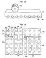
- FIG. 16is a bottom plan view of a resistor array according to one embodiment of the invention.
- FIG. 17is a diagrammatic sectional view depicting a mold during a process according to a further embodiment of the invention.
- FIG. 18is a top plan view of a resistor array according to a further embodiment of the invention during one stage of a manufacturing process.
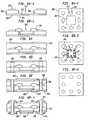
- FIGS. 1 A-Gshow a process for manufacturing inexpensive semiconductor chip packages, according to the one aspect of the '671 disclosure.
- FIG. 1Ashows a side view of a sacrificial layer 100 having a first surface 101 and a second surface 102 .
- the sacrificial layer 100may be comprised of a conductive metallic material, a polymer material or a combination of both a conductive metallic material and a polymer material. Examples of possible sacrificial layer materials include aluminum, copper, steel, iron, bronze, brass, polyimide, polyetherimide, fluropolymer and alloys and combinations thereof.
- the sacrificial layeris comprised of a sheet of aluminum having an approximate substantially uniform thickness of about 100-200 microns; although, the sacrificial sheet could be thicker or thinner in some embodiments.
- a plurality of pads 110are selectively formed, typically by an electroplating operation, so that the pads 110 are disposed on and attached to the first surface 101 of the sacrificial layer 100 .
- the pads 110are arranged on the first surface 101 of the sacrificial layer 100 so as to define a central region 114 between the pads of a particular package group.
- the padsmay be arranged in single rows around the central region 114 or may be arranged in multiple rows in a substantially grid array arrangement, an example of which is shown in FIG. 1D-2.
- the pads 100 in this embodimentare comprised of a first layer of copper 111 and a second layer of gold 112 .
- the pads 110are not critical so long as a good electrical connection can be made thereto. In some embodiments, the pads may resemble posts. Other examples of permissible pad materials include copper, nickel, gold, rhodium, platinum, silver and alloys and combinations thereof.
- the pads 110are all of the same height from the sacrificial layer 100 . However, for higher pin count packages or for other reasons, the pads 110 may not all be of the same height from the sacrificial layer 100 .
- Taller pads 110can be used in outside rows of pads to ensure that the electrical connections between the contacts and the inner pads do not electrically short with the connections between the contacts and the outer pads. This can be useful in cases where the chip contacts are finely spaced or where the contacts are arranged in an area array on the face surface 121 of the chip 100 , an example of which is shown in FIG. 1D-2.
- a back surface 122 of a semiconductor chip 120(or several chips) is next coupled to the sacrificial layer 100 so that the contact bearing face surface 121 of the chip 120 faces away from the sacrificial layer 100 .
- This arrangementis commonly referred to as “back-bonding” a semiconductor chip.
- Any suitable coupling agent 135can be used for such back-bonding.
- a thermally conductive die attach adhesiveis used so that when a heat sink is attached, as described below, there is a more direct thermal path to draw heat away from the chip during thermal cycling. Examples of such preferable adhesive materials include silver filled epoxy, tin-lead solder, boron-nitride, aluminum filled silicone, alumina and copper filled epoxy, among others.
- the chip contacts (not shown) on the face surface 121 of the chip 120are each electrically connected to a respective pad 110 by wire-bonding the one to the other, as shown in FIG. 1D-1.
- the wire-bonded connection 130could take the form of a ball bond/stitch (or wedge) bond combination, as shown, or the wire could be stitch-bonded to both the chip contacts and the pads 110 .
- Other conventionscould be used to interconnect the chip contacts and the pads, such as TAB leads, electroformed beam leads, etc.
- FIG. 1E-2shows a top view of FIG. 1D-1.
- the assemblyincluding the first surface 101 of the sacrificial layer 100 , the pads 110 , the chip 120 and the electrical connections, is next encapsulated (or over-molded) by a flowable, curable dielectric material 140 , as by convention semiconductor molding technology, as shown in FIG. 1E.
- the dielectric materialis typically comprised of filled or unfilled standard thermoset or thermo plastic resins as used in the industry, such as epoxy resin, silicone resin or other plastic encapsulating material. The dielectric material is then fully cured.
- the sacrificial layer 100is next removed, as shown in FIG. 1F.
- the sacrificial layeris removed, using an etching operation, so as to expose the bottom surface 113 of the pads 110 .
- the step of removing the sacrificial layer 100also exposes the thermally conductive die attach adhesive 135 .
- the sacrificial layermay be more selectively removed to provide added features on the bottom of the finished package, such as taller pads 110 which protrude from the bottom of the package, and/or a heat sink disposed beneath and protruding from the bottom of the bottom of the finished package and attached to the back surface 122 of the chip.
- FIG. 1G-1the individual packaged chips 150 are “diced” or separated from each other.
- the exposed bottom surfaces 113 of the pads 110may be attached to respective bond pads on the PWB.
- One method of making such an attachmentis to connect solder balls to the bottom surface 113 of the pads 110 .
- the solder ballsare typically comprised of a combination of tin and lead and may further coat a solid metal ball such that the solder balls are non-collapsing.
- FIG. 1G-2shows a bottom view of a multi-chip module embodiment of the '671 disclosure in which the packages are diced so that more than one chip 120 is included in the resulting package.
- FIG. 1G-2could also be the top view of the undiced packages, as shown in FIG. 1F. While the above process is shown and described in an embodiment that packages more than one chip simultaneously, the process could also be used to package an individual chip if desired.
- the sacrificial layeris comprised of a dielectric polymer sheet 100 ′ having a conductive layer 101 ′, typically a thin layer of copper, on one surface of the sacrificial layer 100 ′, as shown in FIG. 2A.
- An array of conductive pads 110 ′are next photo-lithographically defined by etching away undesired sections of the conductive layer 101 ′ so that the pads 110 ′ define a central region 114 ′ therebetween.
- a central conductive region 115 ′may also be defined by the pad-forming lithographic process, as shown in FIG. 2B.
- a back surface 122 ′ of a semiconductor chip 120 ′is then bonded to the conductive region 115 ′ through the use of the thermally conductive die attach adhesive 135 ′, as discussed in reference to FIG. 1.
- the chip contacts (not shown) on the exposed face surface 121 ′ of the chip 120 ′are then electrically connected to respective pads 110 ′ by wire-bonding wires 130 ′ therebetween.
- the elementsare next encapsulated in FIG. 2D using a suitable liquid encapsulant for the application and the encapsulant 140 ′ is cured. Portions of the polymer sheet 100 ′ are then removed, as by chemically etching or laser ablation operations, so that the pads 110 ′ and central conductive region 115 ′ are exposed.
- a multi-chip packagemay include chips of different sizes that perform different functions.
- the addition of a dielectric, polymer sheet 100 ′allows this multi-chip module to have conductive paths 118 ′ interconnecting at least some of the pads 110 ′ within the multi-chip module thereby allowing signals to be transferred between the chips. It should be noted that if a wiring layer, such as is described in this multi-chip embodiment, is not needed or desired, the entire polymer sheet 100 ′ may simply be removed by chemically dissolving the sheet leaving the pads and the central conductive region exposed.
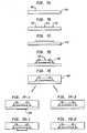
- FIG. 3shows a still further embodiment of a packaged chip, similar to the packaged chips shown in FIG. 1G-1.
- a conductive protrusion 116 ′is electrically connected to a respective pad 110 ′ and extends to the top surface 155 ′ of the finished package 150 ′ so that a top surface 117 ′ of the protrusion 116 ′ is exposed.
- This arrangementallows the bottom surface 113 ′ of the pads 110 ′ to be soldered to a supporting substrate (such as a PWB) while allowing another electronic component and/or semiconductor chip to be electrically connected to the packaged chip via the exposed top surface 117 ′ of the protrusions 116 ′; thus, creating a chip stacking technique.
- the protrusionsmay extend from every pad; however, typically they will extend from less than all of the pads.
- FIG. 4Ashows a side view of a microelectronic component 170 ′′ which is attached to the chip 120 ′′.
- the contacts on such a microelectronic componentmay be electrically connected between respective contacts on the chip 120 ′′ and/or may be connected to respective pads 110 ′′.
- the microelectronic componentis a second semiconductor chip 170 ′′′, as shown in FIG. 4B, the back surface of the second chip 170 ′′′ will be back-bonded to the face surface of the first chip 120 ′′′ and the contacts on the second chip may be electrically connected to the contacts on the first chip 120 ′′′ and/or to respective pads 110 ′′′.
- the pads 110 ′′′themselves may also be electrically interconnected.
- FIG. 5Ashows a sacrificial layer, as earlier described, having a first surface 201 and a second surface 202 .
- FIG. 5Ba plurality of cavities 203 is removed from the first surface 201 of the sacrificial layer 200 .
- an etchable layeris used for the sacrificial layer so that the cavities 203 may simply be etched into the sacrificial layer 200 in the form desired.
- a second photo-imageable dielectric layer 204such as standard photoresist, is disposed on top of the first surface 201 of the sacrificial layer 200 and apertures 205 are developed and removed using standard photo-lithographic techniques so as to control the creation and placement of the cavities.
- Conductive pads 210are next plated into the cavities 203 and apertures 205 so as to create the rivet-like pads 210 , as shown in FIG. 5C. These pads 210 have a bottom bump flange 213 adjacent to the sacrificial layer 200 and integrally attached to a post pad 211 such that the post pad protrudes from the bump flange 213 . A second bump flange 212 is integrally attached to the opposite end of the post pad 211 . Both bump flanges 212 / 213 have flange areas that extend beyond the diameter of the post pad 211 .
- FIGS. 5I-5Jshow alternate cross-sectional pad configurations, according to the present invention. In the embodiment shown in FIG.
- the padis comprised of the bottom bump flange 213 ′ and the post pad 211 ′, depicted in conjunction with sacrificial layer 200 ′.
- the bump flanges 212 ′′ and 213 ′′, shown in conjunction with post pad 211 ′′ and sacrificial layer 200 ′′,are more squared off at the edges when compared to the rounded/oval bump flanges shown in the other FIGS.
- Other shape bump flangesmay also be used.
- FIG. 5Dthe photo-imageable layer 204 is removed leaving the pads 210 such that the pads within a particular group define a central region therebetween.
- a chip 220is next back-bonded to the first surface of the sacrificial layer 200 using a thermally conductive die attach adhesive 235 , as described in the previous embodiment.
- FIG. 5Eshows electrical connections 230 interconnecting the chip contacts (not shown) on the face surface 221 of the chip 220 and the pads 210 .
- the electrical connections 230are made by using a wire-bonder to stitch bond both ends of the wire to the pad 210 and the chip contacts.
- the stitch bondscreate a low profile electrical connection between the contacts and the pads that, in turn, allows the finished package to be thinner.
- the pads 210 , chip 220 , and wires 230are then encapsulated using an encapsulant 240 , as described above in reference to FIG. 1 and further shown in FIG. 5F.
- the sacrificial layeris next etched away to expose the bottom bump flange 213 , as shown in FIG. 2G.
- the packaged chipsare then diced into either individual packaged chips or packaged multi-chip modules, as shown in FIG. 5H.
- FIGS. 6A-6Fshow another stackable chip arrangement.
- FIG. 6A-1shows a side view in which a dielectric base material layer 305 is disposed on a top surface 302 of a sacrificial layer 300 .
- the base material 305is preferably comprised of a dielectric sheet-like layer, such as polyimide. Typically, the base material 305 is laminated onto the sacrificial layer 300 .
- Conductive pads 310are disposed on the base material 305 . The pads 310 may be plated on the base material 305 prior or subsequent to the base material's attachment to the sacrificial layer 300 .
- FIG. 6A-2shows a top plan view of FIG. 6A-1. The pads 310 in FIG.
- FIG. 6A-2has bonding sites 315 and via sites 316 .
- the pads 310further define a central cavity 314 .
- a semiconductor chip 320is then back-bonded to the first surface 302 of the sacrificial layer 300 within the central cavity.
- the chip contacts(not shown) are next electrically connected to respective bonding sites 315 on the pads 310 .
- the contactsare connected to the respective bonding sites 315 by wire bonds 330 .
- FIG. 6B-2shows a top plan view of FIG. 6B-1.
- a curable, liquid encapsulant 340next encapsulates the chip, pads and wires and is cured, as described above.
- a second conductive sacrificial layer 345is then disposed on the exposed surface of the encapsulant 340 .
- the second sacrificial layer 345is typically laminated onto the encapsulant 340 .
- apertures 350are next drilled through the cured dielectric material such that the aperture sidewalls extend through the package from a top surface to a bottom surface thereby creating a via through at least some of the conductive pads 310 at the via sites 316 .
- the sidewalls 355 of the apertures 350are next plated with a conductive metal 360 so that a conductive path is created from one side of the aperture to the next extending completely through the package.
- the conductive metal 360typically terminates on either side of the aperture 350 in flange portions 365 .
- the shape and size of the flange portionsare controlled through standard photo-lithographic means in which a dielectric photoresist 363 is applied to the second sacrificial layer and developed so that the flange area may be removed therefrom.
- the photoresistalso allows the selective plating of a thermally conductive metal layer 368 on the second surface 301 of the first sacrificial layer 300 .
- the first sacrificial layer 300 and the second sacrificial layer 345are both etched such that only the portions under the flange portions 365 and the metal layer 368 remain.
- the second sacrificial layer 345could be selectively etched and used either as a ground/power layer or a wiring layer.
- the flange portions 365 and metal layer 368are made of a material that is resistant to the etching solution used to etch the sacrificial layers.
- the plated conductive viasare next filled with conductive material 370 , such as solder or metal-filled epoxy, so that the conductive material 370 protrudes from the bottom of the vias 371 and at the top of the vias 372 .
- conductive material 370such as solder or metal-filled epoxy
- This arrangementallows the bottom of the via to be electrically connected to a PWB while also allowing the top of the via 372 to be connected to another chip package as in a vertical chip stacking arrangement.
- the metal layermay be connected to a heat sink in the PWB so that heat may be directed away from the chip during operation.
- first sacrificial layer 300 and the metal layer 368may also serve the function of stretching any solder connections between the package and the PWB in order to obtain solder columns which are more able to withstand the expansion and contraction of the package/PWB during thermal cycling of the chip 320 .
- FIGS. 7A-7GA still further embodiment of the '671 disclosure is shown in FIGS. 7A-7G.
- a sacrificial sheet 400comprised of copper is first provided.
- goldis selectively electroplated onto the first surface 401 of the sacrificial sheet 400 so as to define pad regions 410 and a central conductive region 415 positioned between the pad regions 410 , as shown in FIG. 7B.
- the second surface 402 of the sacrificial sheet 400is then covered with a photoresist 418 , as shown in FIG. 7C, and the first surface 401 of the sacrificial sheet 400 is etched.
- the etchant usedshould etch the sacrificial sheet more readily than it etches the gold pads/central region.
- a gold region 450is selectively electroplated on the exposed surface of the sacrificial sheet 400 and the sheet is etched so that only the pads 410 and the central region 415 remain.
- the central regionprotrudes from the bottom of the package allowing it to be more easily attached to a PWB to provide a direct heat path away from the chip during operation of the device.
- the protruding central region 415may also provide a method to stretch the solder balls attaching the exposed pads 410 to the PWB into solder columns so that they are more able to withstand the differential expansion and contraction of the package/PWB during operation of the device.
- the sacrificial sheet 400is etched such that the pads 410 and the central region 415 are planar with respect to the bottom of the package.
- the devicemay then be electrically connected to a PWB through the pads 410 and thermally connected to the PWB through the central region 415 .
- the pads 410may be etched during the sacrificial sheet etching step to create a cavity feature within each pad. These cavities may be used to facilitate solder ball placement on the pads 410 .
- Variants of the methods described above for manufacturing a semiconductor packageare also applicable to resistor manufacturing.
- a resistoris a component that has electrical resistance. Resistors can be used to control the flow of current and/or to provide a desired voltage-to-current relationship.
- FIG. 8Ashows a side view of a sacrificial layer 800 having a first surface 801 and a second surface 802 .
- the sacrificial layer 800may be comprised of an electrically conductive metallic material, a polymer material or a combination of both a conductive metallic material and a polymer material.
- the sacrificial layeris formed from an electrically conductive material such as a metal. Examples of conductive sacrificial layer materials include aluminum, copper, steel, iron, bronze, brass, and alloys and combinations thereof.
- an apertured layer 803is applied across the first surface 801 of the sacrificial layer 800 .
- the apertured layer 803desirably is formed from a material which is substantially resistant to the etchant used to etch the sacrificial layer as discussed below.
- the apertured layercan be provided with apertures 804 before uniting the apertured layer with the sacrificial layer, as by punching or drilling apertures in a preformed solid layer such as a solid sheet of polymer or metal, or by forming the layer with the apertures in a conventional mold such as an injection mold or compression mold.
- the apertured layermay be formed in place on the first surface 801 by applying a continuous layer of a patternable material such as a photoresist onto the first surface 801 of the sacrificial layer and exposing the patternable material to light or other radiation in a pattern corresponding to a positive or negative image of the apertures to be formed, depending upon the type of photoresist employed.
- the photoresistis then developed and processed form apertures 804 using standard photo-lithographic techniques so as to control the creation and placement of cavities.
- the apertured layermay also be formed by selectively depositing the etch-resistant material onto the first surface of the sacrificial layer as, for example, by screen printing the material in a fluid condition using a process which leaves uncoated spots on the surface, and then curing the deposited material to form a solid layer with apertures at the uncoated spots.
- the apertured layermay also be a reusable mask.
- portions of the sacrificial layer 800 aligned with the apertures 804 of the apertured layer 803are removed, such as by using an etching process, in order to create cavities 805 within the sacrificial layer 800 .
- the cavities 805may be formed in single rows on the first surface 801 of the sacrificial layer 800 or in any other desired pattern, in a similar fashion to the arrangement shown in FIG. 1D-2.
- the cavities 805form depressions in the first surface 801 of the sacrificial layer 800 extending toward the second surface 802 thereof.
- the size and shape of the cavities 805may be controlled by controlling the etching process utilized.
- the first surface 801can be exposed to an alkaline etch solution. Increasing the exposure time increases the size of the cavities.
- the second surface 802 of the sacrificial layeris protected from the etchant during this stage of the process, as by a suitable temporary coating or fixture (not shown).
- a layer of a first conductive material 806is then deposited in the cavities 805 , such as by using a deposition, plating or immersion coating process.
- the first conductive material 806can be copper, gold, nickel, platinum or other metal that can be deposited.
- the first conductive material 806preferably is resistant to the etchant which is used to remove the sacrificial layer in a subsequent stage of the process discussed below.
- the first conductive materialalso should be resistant to chemicals used to remove the apertured layer as discussed below.
- the first conductive materialis a material which can be readily soldered during use of the finished resistor.
- a second conductive materialis deposited in each cavity 805 to form conductive pads 807 which include both the first conductive material 806 and the second conductive material.
- the second conductive materialmay be comprised of conductive materials such as copper, or highly conductive materials such as silver or gold.
- highly conductive materialssuch as silver or gold is that their surface or contact resistance does not change greatly. For example, gold does not become oxidized, and silver remains very conductive after it becomes oxidized.
- the second conductive materialis deposited in each cavity 805 atop the first layer of conductive material 806 , preferably by electroplating.
- a first conductive material 806may not be required.
- an immersion coating processis performed wherein the aluminum is coated with zinc by autoreduction of zinc ions in solution onto the exposed aluminum. This process is performed so that the aluminum sacrificial layer can be directly platable.
- the second conductive materialis deposited in each cavity 805 atop the seed layer.
- Each pad 807has a bottom bump flange 808 adjacent to the sacrificial layer 800 and a post 809 such that the pad 809 protrudes upwardly from the bottom bump flange 808 , through an aperture 804 in the sacrificial layer.
- a top bump flange 810is integrally attached to the opposite end of the post 809 . Both bump flanges 810 and 808 have flange areas that extend beyond the diameter of the post 809 .
- the top bump flange 810extends over the apertured layer 803 . Stated another way, the flanges 810 and 808 of each pad 807 are wider than the post 809 of such pad.
- the conductive pads 807are generally rivet-shaped.
- the alternate cross-sectional pad configurations discussed above with reference to FIGS. 5I and 5Jalso can be used.
- the apertured layer 803is then removed from the first surface 801 of the sacrificial layer 800 .
- a suitable photoresist stripperis employed to remove the photoresist.
- an etching solutionis used to remove the photoresist, the etching solution need only be capable of removing the particular photoresist being used. The type of etching solution varies depending on the metal used for the photoresist. If a copper apertured layer is used, acidic cupric chloride or ammonical copper etching solutions could be used to remove the copper photoresist.
- an aluminum apertured layeris used, a caustic solution with additives to control etch activity will work.
- the etchant used to remove the apertured layerpreferably does not appreciably attack the conductive material or materials in the pads 807 , or the sacrificial layer 800 .
- the top bump flanges 810are spaced above the first surface 801 of the sacrificial layer 800 .
- a resistive materialis deposited over the first surface 801 of the sacrificial layer 800 such that a resistive layer 811 covers the first surface 801 of the sacrificial layer 800 and the conductive pads 807 .
- the resistive materialmay be comprised of any conductive or semiconductive material. Most preferably, the resistive material is applied in a liquid, paste or other flowable condition, and cured to form a solid mass.
- the resistive materialis comprised of conductive particles such as one or more metals, graphite or other carbon particles dispersed in a polymeric resin, fusible glass or other binder.
- conductive particlessuch as one or more metals, graphite or other carbon particles dispersed in a polymeric resin, fusible glass or other binder.
- the binderalso may include mixtures of two or more materials.
- the resistive materialcan be deposited using an injection molding process.
- the resistive materialcan also be deposited using methods such as spin coating, casting, roller or doctor blade coating, silk-screening, stenciling and compression molding. In the particular process depicted in FIGS.
- the resistive materialis applied as a single continuous layer.
- the resistive material and padsform a single unit, with the top bump flanges 810 and posts 809 of all of the pads 807 being embedded in the mass 811 .
- the sacrificial layer 800is removed to expose the bottom bump flanges 808 .
- the sacrificial layer 800can be removed using processes such as chemical etching or plasma etching (wet or dry). While an etching process is the preferable method of separating the sacrificial layer 800 , any other procedure capable of removing the sacrificial layer without destroying the unit including the resistive material and pads can be employed. For example, the sacrificial layer may be more selectively removed, leaving portions of the sacrificial layer in place but still exposing the conductive pads.
- the remaining portions of the sacrificial layerprovide added features on the bottom of the finished resistor, such as a heat sink disposed beneath and protruding from the bottom of the finished resistors.
- the cured resistive material and padsdo not strongly adhere to the sacrificial layer, or where the adhesion can be released without destroying the unit including the resistive material and pads the sacrificial layer 800 can be peeled away from the unit, preferably without destroying the sacrificial layer. Differential expansion in materials may cause the sacrificial layer 800 to become separated from the resistive layer 811 and the conductive pads 807 .
- the material constituting the pads 807such as the first conductive material 805 immediately adjacent to the sacrificial layer, may have a high coefficient of thermal expansion (CTE), and sacrificial layer 800 may be formed from polished stainless steel.
- CTEcoefficient of thermal expansion
- sacrificial layer 800may be formed from polished stainless steel.
- the conductive material 805would not adhere well to the stainless steel sacrificial layer 800 , and the expansion of the material 805 , during a process of applying the resistive material such as injection molding, would cause separation of the sacrificial layer 800 and the resistor unit.
- the conductive material forming the interface between the pads and the sacrificial layermay have a melting temperature below the melting and degradation temperatures of the other elements in the unit, so that the pads can be separated from the sacrificial layer 800 by bringing the assembly to an elevated temperature.
- the exposed bottom bump flanges 808remain coated with the first conductive material layer 806 described above in reference to FIG. 8D. This material 806 enhances the solderability of the conductive pads 807 .
- the resistance of the resulting devicecan be varied based upon which bottom bump flanges 808 are connected. A greater resistance can be created by increasing the distance between connected bottom bump flanges 808 .
- the unitary resistive layer 811can be cut, severed, diced or laser trimmed to subdivide the single unit into a plurality of individual resistors, each including a portion of the resistive layer and two or more of the conductive pads 807 .
- the resistive layer 811 of FIG. 8Hhas been cut into four separate resistors 812 A, 812 B, 812 C and 812 D. Although four resistors have been manufactured in FIG. 8I, any number of resistors may be formed. Alternatively, the subdividing step may be omitted, and the unit including the entire resistive layer 811 may be used as a single resistive element.
- cavities 805 in the sacrificial layercan be formed by processes other than by etching through the apertures in the apertured layer.
- the cavitiescan be formed using an embossing tool or stamping die, or the sacrificial layer can be cast or otherwise formed with the cavities in the first surface.
- An apertured layer with pre-formed aperturescan be assembled to the sacrificial layer so that the apertures are in alignment with the cavities.
- a patternable layersuch as a photoresist can be applied onto the first surface and subsequently patterned to form the apertures.
- Processes other than electroplatingcan be employed to deposit the conductive material or materials in the cavities and in the apertures of the apertured layer.
- a metal-filled polymer materialcan be used instead of a second conductive material.
- the metal-filled polymer materialcan be deposited into the cavities by using a squeegee followed by a uniform coating with a doctor blade to planarize.
- the metal-filled polymer materialfills each cavity 805 and aperture 804 , so as to form the bottom flanges 808 and posts 809 of the conductive pads 807 .
- Additional conductive metal-filled polymerthen can be applied in spots on the top surface of the apertured layer 803 , as by silk-screening, to form the top flanges 810 of the pads.
- the amount of metal-filled polymer applied in each cavity and aperturemay be slightly greater than the volume of such cavity and aperture, so that the excess forms the top flange 810 .
- the sacrificial layer 800need not be formed from an electrically conductive material. Materials such as nonconductive polymers can be employed.
- the polymer sacrificial layercan be removed from the resistive unit by laser or water jet erosion or drilling, or by dissolving the sacrificial layer using a solvent which does not substantially attack the cured resistive material.
- Polymeric sacrificial layers with cavitiescan be formed, for example, by injection molding, thermoforming, compression molding and the like.
- an electrically conductive coating or “seed layer”may be applied on the first surface, including those portions of the first surface defining the cavities.
- the seed layermay include nickel, chromium, a nickel-copper alloy such as Monel® or another suitable alloy vacuum deposited or sputter-deposited on the first surface of the polymer sacrificial layer, or electrolessly plated onto the first surface. If the material of the seed layer adheres to the finished resistor unit after removal of the sacrificial layer, the seed layer may be removed by a brief etching process or microelectronic-abrasive pressure blast.
- FIGS. 9A-9Hshow another method of manufacturing resistors according to the present invention.
- the sacrificial layer 900(FIG. 9A) has a first surface 901 and a second surface 902 .
- the sacrificial layer 900may be comprised of any of the materials discussed above.
- an apertured layer 903is applied across the first surface 901 of the sacrificial layer 900 using one of the methods previously discussed.
- FIG. 9Cportions of the sacrificial layer 900 aligned with the apertures 904 of the apertured layer 903 are removed in order to create cavities 905 within the sacrificial layer 900 .
- the cavities 905can be formed using an etching process with apertured layer 903 serving as an etch mask, or can be formed before the apertured layer is placed on the first surface. As previously discussed, the cavities may be formed in rows in the first surface of the sacrificial layer 800 or in any other pattern.
- each shellmay be formed from a single metal.
- a film of a first metalis applied first, followed by a further layer of a second metal defining the interior surface of the shell, facing toward the interior space.
- each shell or pad 906 and the resistive material 908 (FIG. 9G) within the shellforms a projection extending from the bottom surface of the resistive layer.
- the sacrificial layer 900is removed from the unit including the resistive layer and pads, using any of the methods previously described. As previously discussed, the sacrificial layer may be selectively removed, leaving portions of the sacrificial layer in place to provide added features on the bottom of the unit, such as a heat sink disposed beneath and protruding from the bottom of the finished product. Finally, as shown in FIG. 9H, the resulting resistor unit can be subdivided into a plurality of individual resistors, although the entire unit as shown in FIG. 9G can also be used as the finished product.
- the apertured layer 903may be left in place when the resistive material is deposited, so that the resistive material is filled into the interior spaces 911 of the shells 906 through the apertures 904 .
- the apertured layercan be stripped away after removal of the sacrificial layer from the resistive unit.
- the apertured layercan be left in place and may form part of the finished product. If the unit is subdivided, the apertured layer can be subdivided along with the resistive layer.
- FIG. 10Ashows a side view of a sacrificial layer 1000 having a first surface 1001 and a second surface 1002 .
- the sacrificial layer 1000may be comprised of a conductive material, desirably a metallic material.
- the first surface 1001 of the sacrificial layer 1000optionally is roughened or otherwise treated to enhance adhesion of the resistive layer to the sacrificial layer.
- the first surfacemay be roughened by sanding, sandblasting, or other conventional mechanical processes.
- the first surfacemay be roughened by electroplating this surface with a metal such as nickel under conditions which promote formation of a rough, dendritic plating deposit.
- resistive materialis then deposited onto the first surface 1001 of the sacrificial layer 1000 to form a resistive layer 1003 .
- the resistive materialcan be deposited in a fluid condition as discussed above, or else may be in a substantially solid condition.
- a solid layer of resistive materialcan be laminated with the sacrificial layer under conditions such as heat and pressure which promote adhesion of the resistive layer and the sacrificial layer.
- an etch-resistant material 1006is deposited onto the second surface 1002 at locations where pads are to be provided in the finished unit.
- an apertured layer 1004is applied across the second surface 1002 of the sacrificial layer 1000 , as, for example, by applying a continuous layer of a patternable material such as a photoresist and exposing and developing the photoresist to form apertures 1006 in the locations where the pads are desired.
- a relatively etch-resistant conductive cover material 1006is applied on the second surface 1002 of the sacrificial layer 1000 in the apertures 1005 , using any of the methods of depositing conductive materials disclosed herein or known in the art.
- the conductive cover material 1006desirably is a metal such as gold, osmium, rhodium, platinum, tin, nickel, chromium and alloys thereof.
- the conductive cover materialis a metal which can remain as part of the pads in the finished unit, for example, where the cover material desirably is a readily solderable metal.
- the apertured layer 1004is removed from the second surface 1002 of the sacrificial layer 1000 using any of the methods previously discussed or known in the art.
- the sacrificial layer 1000is etched so that a plurality of electrodes 1007 remains.
- the etch-resistant cover material 1006protects portions of the sacrificial layer. Those protected portions form the electrodes.
- the cover materialis a photoresist or other material which does not form part of the completed pads. In this embodiment, the cover material is removed after the etching step.
- FIGS. 11A-11Eshow another method of manufacturing resistors according to the present invention.
- the sacrificial layer 1100 and the conductive pads 1107are placed in the interior 1111 of injection mold 1110 , such that the second surface 1102 of the sacrificial layer 1100 lies on one interior surface 1112 of the injection mold 1110 .
- An insulating layer 1120 having a first or top surface 1122 and a second or bottom surface 1124is also placed in the interior 1111 of the injection mold 1110 , such that the first surface 1122 of the insulating layer 1120 faces an interior surface 1126 of the injection mold 1110 opposite from surface 1112 .
- the insulating layercan be comprised of materials such as ceramic, glass or a high temperature plastic.
- the insulating layer 1120has a coefficient of thermal expansion similar to that of the resistive material.
- the insulating layer 1120 and sacrificial layer 1100are secured to the mold 1110 by appropriate holding devices (not shown); by applying a vacuum through ports (not shown) in mold surfaces 1126 and 1112 ; or by adhesives.
- the adhesives usedare adapted to degrade or release their bond upon application of heat. Because the sacrificial layer 1100 rests on an upwardly-facing, horizontal mold surface 1112 in the particular arrangement illustrated, the sacrificial layer may be held in place by gravity.
- a resistive materialis injected into the interior 1111 of the injection mold 1100 between the first surface 1101 of the sacrificial layer 1100 and the second or bottom surface 1124 of the insulating layer 1120 such that the bottom surface 1124 of the insulating layer 1120 , the conductive pads 1107 and the first surface 1101 of the sacrificial layer 1100 are covered by the resistive material.
- the injection-molded resistive materialforms resistive layer 1140 .
- the resistive layer 1140 , conductive pads 1107 and insulating layer 1120form a unit 1160 .
- the resulting unit 1160 and the sacrificial layer 1100are removed from the injection mold 1110 .
- the top surface 1122 of the insulating layer 1120is secured to the upper inner surface 1126 of the injection mold 1110 through the use of a heat releasable adhesive, and where the resistive material 1140 is injected at elevated temperature, the adhesive bond is released to a nonadherent material at molding temperature, facilitating the removal of the molded device 1160 from the injection mold 1110 .
- the molded unit 1160can be ejected from the injection mold 1110 using positive air pressure applied through the vacuum ports.
- the sacrificial layermay be removed to expose the bottom bump flanges 1108 using the methods described above.
- the insulating layer 1120acts as a common base, so that the resulting resistive layer 1140 , the conductive pads 1107 and the insulating layer 1120 form an integrated passive device.
- the resistive material of the unitcan be subdivided, as by cutting, sawing, or laser trimming, to provide a plurality of individual resistors 1150 A, 1150 B mounted on the same insulating layer 1120 .
- the individual resistors 1150 A, 1150 B and the insulating layer 1120together form an integrated passive device.
- the entire unit, including the insulating layercan be subdivided, as by cutting through the insulating layer and the resistive layer, to form a plurality of separate units, each including a portion of the resistive layer, a portion of the insulating layer, and a plurality of conductive pads.
- a similar processcan be performed using sacrificial layers having other configurations as, for example, using the sacrificial layer and pads shown in FIG. 9E and the sacrificial layer of FIG. 10B.
- the step of applying the resistive layercan be performed using the injection molding process discussed above with reference to FIGS. 11A-11E. Also, the injection molding process can be used without the insulating layer.
- a non-conductive apertured layer 1210which is thicker than the patternable layer used in the embodiments shown in FIGS. 8A-8I, is applied across the first surface of the sacrificial layer.
- Pads 1230 and posts 1240are formed as discussed above with reference to FIGS. 8A-8I, so that the top bump flanges 1231 are initially in contact with the surface of the apertured layer.
- the apertured layer 1210is etched or dissolved from the first surface of a sacrificial layer (not shown). However, the etching or dissolving process is arrested before the entire apertured layer 1210 has been removed and a portion of layer 1210 remains on the first surface of the sacrificial layer.
- a hot caustic solutioncan be used to remove a portion of the patternable layer 1210 .
- An etch ratemay be selected for the hot caustic solution such that only a portion of the patternable layer is removed.
- the remaining portion of the apertured layerdefines a top surface 1211 recessed below the top bump flanges 1231 .
- the resistive materialis applied over this surface 1211 .
- the bottom bump flanges 1230are exposed and extend below the remaining patternable layer 1210 .
- some or all of the sacrificial layermay be removed from the remaining apertured layer 1210 before the resistive material is applied; the apertured layer will hold the conductive pads in place during application of the resistive material.
- the remaining apertured layer 1210provides an insulating layer at lower surface 1222 of the resistive material 1220 .
- This layer 1210effectively insulates the resistive material 1220 from whatever device the finished resistive device is mounted on. Further, depending upon the material chosen for the apertured layer 1210 , the remaining apertured layer 1210 may provide mechanical support for the resistive device and may block moisture from the resistive material 1220 .
- the conductive pads 1302may be elongated in a direction of elongation L along the surface of the resistive unit.
- the particular pads shown in FIG. 13are manufactured by the process as discussed above with reference to FIGS. 9A-9H, but similar elongated pads can be provided by any of the processes described above.
- the elongated padscan provide for greater mechanical stability. Elongated pads can have greater mechanical strength than round pads having a diameter equal to the narrow dimension of the elongated pads.
- elongated conductive padsact to spread current in the direction of elongation, and thus tend to suppress the effect of local variations in electrical resistivity within the resistive layer 1301 .
- a resistive device 1400includes pads 1402 , resistive layer 1403 and a heat sink 1404 overlying the top surface of the resistive layer, remote from the pads 1402 .
- the heat sink 1404is formed from a thermally-conductive material such as, for example, aluminum. Where the material of the heat sink is electrically conductive, a thin dielectric layer 1408 is provided between the base surface 1406 of the heat sink 1404 and the resistive layer 1403 .
- the base surface 1406 of the heat sinkmay be treated with an insulating finish such as epoxy or anodized.
- a dielectric layermay be provided on the resistive layer as, for example, by a molding process as discussed above with reference to FIGS. 11A-11E, or by laminating the dielectric layer to the resistive layer.
- the heat sink and dielectricmay be provided as a unit which is applied in place of a simple dielectric layer in a molding process as described with reference to FIGS. 11A-11E.
- the heat sink 1404allows the resistive device 1400 to dissipate more power without overheating. While the resistive device 1400 as shown in FIG. 14 is manufactured by the method as shown in FIGS. 9A-9H, resistive devices manufactured by any other method of manufacturing resistors described herein may be mounted onto a heat sink in similar fashion.
- resistive materialcan be removed from the resistive unit manufactured in accordance with the processes discussed above using a bulk trimming process.
- the term “bulk trimming process”refers to a process which reduces the thickness of an entire layer of resistive material, or which brings a layer of non-uniform thickness to a uniform thickness, as by removing high spots in the layer.
- Mechanical bulk timing processesinclude milling using a milling cutter 1510 ; grinding and lapping. Chemical processes such as etching the exposed surface of the resistive layer also may be employed.
- the method or device used to trim away bulk resistive materialdepends upon the demands of the resistor device being manufactured. By controlling the thickness of the resistive material 1500 , resistor values can be modified to a desired value.
- One advantage of the methods of manufacturing resistors using a single sacrificial layer discussed previouslyis that a bulk trimming process can be used before removal of the sacrificial layer. The sacrificial layer reinforces the resistive layer during the bulk trimming process.
- a unit including a layer of resistive material with conductive padscan be cut into patterns forming resistor networks connected between the pads.
- the resistor networks 1601 - 1606 shown in FIG. 16are merely exemplary.
- the resistance between any two pads of such a networkis determined in part by the resistivity of the resistive layer, and in part by the size and shape of layer portions connecting the two pads.
- the resistivity of the layeris controlled by the thickness and composition of the layer, as discussed above.
- the size and shape of the layer portions between any two padscan be set when the network is cut out of the resistive layer.
- network 1601provides a relatively low resistance between pad 1611 a and pad 1611 b , and a higher resistance between pad 1611 a and pad 1611 d .
- Resistanceis proportional to the length of the resistor device between any two pads and inversely proportional to the cross-sectional area of the resistor device in the region between the two pads.
- Methodssuch as mechanical cutting of individual units, die cutting, stamping or laser cutting can be used to separate the individual resistor networks from the layer and to fix the horizontal dimensions of the various parts of the individual resistor networks.
- the horizontal dimensionsare the dimensions in the directions parallel to the surfaces of the layer.
- Discrete value setting or customization of resistorscan be achieved.
- the individual resistor networkscan be further trimmed by selectively removing portions of the network.
- each assemblycan be overmolded after resistor trimming.
- the individual resistor networkscan be formed as individual units by applying the resistive material in discrete masses, rather than in continuous layers.
- a mold 1650FIG. 17
- ribs 1654projecting into the interior of the mold cavity, towards the sacrificial layer 1652 .
- Each ribdefines a narrow gap 1656 adjacent the sacrificial layer.
- the ribscan completely isolate the various portions of the resistive layer from one another during the molding process.
- the ribsmay be arranged to abut the sacrificial layer when the mold is fully closed; the resistive material may be injected or placed in the mold before the mold is fully closed.
- the gaps or open spaces 1620 within individual resistor networksalso may be formed by such a molding process.
- each resistor unit or arrayBy taking a resistor unit or array and slicing it into a series of elongated strips 1701 - 1704 (FIG. 18), and subsequently dividing each elongated strip 1701 - 1704 into still smaller pieces 1710 , 1711 , 1712 , 1713 , for example, a number of resistors of identical or varied resistance can be created.
- Each such resistordesirably includes at least one conductive pad at each end of the resistor.
- each resistormay include only one conductive pad of any of the types described above, the conductive pad being disposed on a bottom surface of the resistive layer.
- a second connectionmay be provided by a conductive element of any type disposed on the top surface of the resistive layer, or on an edge of the resistor.
- the individual resistorscan be trimmed to the desired resistance values, using the methods discussed above, to selectively remove resistor material and provide a resistor of a preselected value to a high degree of accuracy.
Landscapes
- Engineering & Computer Science (AREA)
- Microelectronics & Electronic Packaging (AREA)
- Computer Hardware Design (AREA)
- Power Engineering (AREA)
- Physics & Mathematics (AREA)
- Condensed Matter Physics & Semiconductors (AREA)
- General Physics & Mathematics (AREA)
- Manufacturing & Machinery (AREA)
- Semiconductor Integrated Circuits (AREA)
- Apparatuses And Processes For Manufacturing Resistors (AREA)
- Cooling Or The Like Of Semiconductors Or Solid State Devices (AREA)
- Encapsulation Of And Coatings For Semiconductor Or Solid State Devices (AREA)
Abstract
Description
- The present invention is a continuation of U.S. patent application Ser. No. 09/950,761, filed on Sep. 12, 2001; which is a divisional of U.S. patent application Ser. No. 09/732,821, filed Dec. 7, 2000; which is a continuation-in-part of U.S. patent application Ser. No. 09/409,205, filed Sep. 30, 1999, now U.S. Pat. No. 5,294,830; which is a divisional of U.S. patent application Ser. No. 09/085,352 filed May 27, 1998, now U.S. Pat. No. 6,093,584; which is a continuation of U.S. patent application Ser. No. 08/634,464 filed Apr. 18, 1996, now U.S. Pat. No. 6,001,671. The disclosures of said applications and patents are hereby incorporated by reference herein.[0001]
- The present invention generally relates to a resistor network having multiple different or common values in a single device manufactured using a single sacrificial layer.[0002]
- Resistors are presently fabricated using a number of different methods, depending on the requirements of the circuit in which resistors are to be used. Resistor types such as thin film resistors, thick film resistors, wound wire resistors, molded axial leaded resistors, surface mount resistors and others are known in the art.[0003]
- Thin film resistors are fabricated by first depositing a resistive material, then a conductor material, onto a substrate. A wide variety of substrate materials can be used, but these materials generally contain an oxygen compound to permit adhesion of the resistive film. Materials used for thin film resistors generally must also be capable of providing adhesion to a substrate. The resistor film forms as single points on the substrate in the vicinity of substrate faults or other irregularities that might have an excess of broken oxygen bonds. The points expand into islands that form continuous films.[0004]
- This differs from typical thick film resistor fabrication for which the conductor is deposited first onto a substrate, followed by the resistive material. In general, thick film resistors are formed by adding metal oxide particles to glass particles and firing the mixture at a certain temperature and for a predetermined time period sufficient to melt the glass and sinter the oxide particles together. The resulting structure consists of a series of three-dimensional chains of metal oxide particles embedded in a glass matrix. The higher the metal oxide-to-glass ratio, the lower the resistivity.[0005]
- The drawback of traditional thick and thin film resistor manufacturing is that both processes tend to have many process steps. Another drawback to these methods of manufacture is that they are generally not capable of providing resistor networks having multiple different or common values in a single device. Further, current methods of manufacturing resistors generally result in the leads being located at the periphery of the resistor device. Peripherally located leads often suffer from the problem that these leads can be easily bent, requiring, in certain circumstances, that the resistor be glued in place. The proposed methods are more versatile than existing methods in that a wide range of resistor devices can be built using a single sacrificial layer, and that the resistor devices can be designed without peripherally located leads.[0006]
- One aspect of the present invention provides methods of making resistors. A method of making resistors in accordance with this aspect of the invention desirably includes the steps of providing a sacrificial layer having a first surface and one or more pads including at least one electrically conductive material disposed over at least one region of said first surface, and depositing a resistive material over the pads and over said first surface of said sacrificial layer to thereby form at least one unit including the resistive material and the pad or pads. Following deposition of the resistive material, at least a portion of the sacrificial layer is removed so as to expose the one or more pads. Most preferably, a plurality of resistors is manufactured simultaneously using a single sacrificial layer. The method further may include separating at least some of said resistors from one another, typically after removing the sacrificial layer. For example, the resistive layer may form a large unit including numerous pads and a unitary resistive layer, and such unit can be subdivided to form individual resistors or resistor networks, each including a portion of the layer and at least one pad, and typically at least two pads.[0007]
- The step of providing the sacrificial layer and the pads preferably includes depositing the conductive material onto said first surface of said sacrificial layer. In certain preferred embodiments, cavities are provided in the first surface of the sacrificial layer and the step of depositing the conductive material includes depositing at least one conductive material into these cavities. The step of providing said cavities in the first surface of the sacrificial layer desirably includes providing an apertured layer on the first surface and etching said first surface through the apertures in said apertured layer. For example, the apertured layer may be provided by providing a layer of a patternable material such as a photoresist and exposing the patternable material to light or other radiation in a pattern, and then developing the photoresist to form the apertures.[0008]
- The conductive material of the pads may be deposited through the apertures, so as to form each pad with a bottom flange beneath the apertured layer, within a cavity, a post extending through an aperture, and a top flange overlying the top surface of the apertured layer. The apertured layer may be partially or completely removed, so as to leave the top flanges of the pads elevated above the surface of the sacrificial layer or above the surface of the remaining part of the apertured layer. The resistive material can be applied in a flowable state, as, for example, by molding, calendaring or coating, so that the resistive material encapsulates the top flanges and posts, thus firmly uniting the pads with the resistive material.[0009]
- In a method according to a further aspect of the invention, the pads may be formed as hollow shells within the cavities of the sacrificial layer. The resistive material may penetrate into the interior spaces within these hollow shells.[0010]
- A method of making resistors according to a further aspect of the invention desirably includes the steps of providing a sacrificial layer having a first surface and a second surface; depositing resistive material over the first surface of said sacrificial layer so that the resistive material adheres to the sacrificial layer; and selectively removing portions of the sacrificial layer to form one or more pads connected to said resistive material. For example, spots of an etch-resistant material can be applied to the second surface of the sacrificial layer, and the second surface can be exposed to an etchant so that portions of the sacrificial layer are left in place as individual pads where the etch-resistant material was applied.[0011]
- Methods according to the foregoing aspects of the invention provide efficient manufacturing processes for forming resistors and for forming resistor networks incorporating plural resistances. The resistors and resistor networks can be compact, and can be particularly well-suited to circuit manufacturing techniques such as surface mounting on a printed circuit board or other circuit panel.[0012]
- Still further aspects of the invention provide resistors and resistor networks.[0013]
- Because understanding of the present invention can be facilitated by understanding of the disclosure in the aforementioned U.S. Pat. No. 6,001,671 (hereinafter “the '671 disclosure”), certain portions of the '671 disclosure are reproduced hereinbelow.[0014]
- FIGS.[0015]1A through1G-1 show a side view of a method of manufacturing a semiconductor chip package, according to the '671 disclosure.
- FIG. 1E-2 shows a top view of FIG. 1D-1 in which several chips are back-bonded to a sacrificial layer and electrically connected thereto prior to the encapsulation step, according to the '671 disclosure.[0016]
- FIG. 1D-2 is a top plan view of a chip and sacrificial layer according to another embodiment.[0017]
- FIG. 1G-2 shows a bottom view of a multi-chip embodiment of FIG. 1G-1 after the sacrificial layer has been removed, according to the '671 disclosure.[0018]
- FIG. 2A through 2E show a side view of an alternate method of manufacturing a semiconductor chip package, according to the present invention.[0019]
- FIG. 2F shows a top view of a multi-chip package embodiment of FIG. 2E, according to the '671 disclosure.[0020]
- FIG. 3 shows a side view of a chip package having protrusions extending vertically from one side of the package to the other, the protrusions being electrically connected to at least some of the pads, according to the '671 disclosure.[0021]
- FIG. 4A shows a side view of a chip package having a separate electronic component above the chip in the encapsulated package, according to the '671 disclosure.[0022]
- FIG. 4B shows a side view of a chip package having a second semiconductor chip back-bonded to the first chip such that the chip contacts of both chips and the pads may be interconnected, according to the '671 disclosure.[0023]
- FIGS. 5A through 5H show a side view of an alternate method of manufacturing a semiconductor chip package, according to the '671 disclosure.[0024]
- FIGS. 5I and 5J show a side view of alternate embodiments of the pad/post structure shown in FIGS. 5A through 5H, according to the '671 disclosure.[0025]
- FIGS. 6A-1 through[0026]6F-1 show a side view of an alternate method of manufacturing a semiconductor package having vias extending from one side of the package to the other, according to the '671 disclosure.
- FIG. 6A-2 shows a top view of FIG. 6A-1, according to the '671 disclosure.[0027]
- FIG. 6B-2 shows a top view of FIG. 6B-1.[0028]
- FIG. 6F-2 shows a bottom view of FIG. 6F-1.[0029]
- FIGS. 7A through 7E show a side view of an alternate method of manufacturing a semiconductor chip up to the encapsulation step, according to the '671 disclosure.[0030]
- FIGS. 7F-1 and[0031]7G-1 show a first method of finishing the chip package shown in FIG. 7E.
- FIGS. 7F-2 and[0032]7G-2 show a second method of finishing the chip package shown in FIG. 7E.
- FIGS. 8A through 8I are diagrammatic sectional views depicting successive stages in a method of making resistors, according to one embodiment of the present invention.[0033]
- FIGS. 9A through 9H are diagrammatic sectional views depicting successive stages in a method of making resistors, according to another embodiment of the present invention.[0034]
- FIGS. 10A through 10G are diagrammatic sectional views depicting successive stages in a method of making resistors, according to a further embodiment of the present invention.[0035]
- FIGS. 11A through 11E are diagrammatic sectional views depicting successive stages in a method of making resistors, according to yet another embodiment of the present invention.[0036]
- FIG. 12 is a diagrammatic sectional view depicting a resistor in accordance with yet another embodiment of the present invention.[0037]
- FIG. 13 is a perspective view of a resistor according to yet another embodiment of the invention, manufactured by a method as shown in FIGS. 9A-9H.[0038]
- FIG. 14 is a perspective side view of a resistor in conjunction with a heat sink.[0039]
- FIG. 15 is a diagrammatic view depicting a bulk sheet trimming process according to a further embodiment of the invention.[0040]
- FIG. 16 is a bottom plan view of a resistor array according to one embodiment of the invention.[0041]
- FIG. 17 is a diagrammatic sectional view depicting a mold during a process according to a further embodiment of the invention.[0042]
- FIG. 18 is a top plan view of a resistor array according to a further embodiment of the invention during one stage of a manufacturing process.[0043]
- FIGS.[0044]1A-G show a process for manufacturing inexpensive semiconductor chip packages, according to the one aspect of the '671 disclosure. FIG. 1A shows a side view of a
sacrificial layer 100 having afirst surface 101 and asecond surface 102. Thesacrificial layer 100 may be comprised of a conductive metallic material, a polymer material or a combination of both a conductive metallic material and a polymer material. Examples of possible sacrificial layer materials include aluminum, copper, steel, iron, bronze, brass, polyimide, polyetherimide, fluropolymer and alloys and combinations thereof. In FIG. 1A, the sacrificial layer is comprised of a sheet of aluminum having an approximate substantially uniform thickness of about 100-200 microns; although, the sacrificial sheet could be thicker or thinner in some embodiments. - In FIG. 1B, a plurality of[0045]
pads 110 are selectively formed, typically by an electroplating operation, so that thepads 110 are disposed on and attached to thefirst surface 101 of thesacrificial layer 100. Thepads 110 are arranged on thefirst surface 101 of thesacrificial layer 100 so as to define acentral region 114 between the pads of a particular package group. The pads may be arranged in single rows around thecentral region 114 or may be arranged in multiple rows in a substantially grid array arrangement, an example of which is shown in FIG. 1D-2. Thepads 100 in this embodiment are comprised of a first layer ofcopper 111 and a second layer ofgold 112. Typically, there is also a center barrier layer (not shown) of nickel to ensure that the copper and gold layers do not diffuse into one another. Thegold layer 112 facilitates a bond that is made by the electrical connection to the chip contacts, as described in more detail below. The height of thepads 110 is not critical so long as a good electrical connection can be made thereto. In some embodiments, the pads may resemble posts. Other examples of permissible pad materials include copper, nickel, gold, rhodium, platinum, silver and alloys and combinations thereof. Typically, in a low pin count package, thepads 110 are all of the same height from thesacrificial layer 100. However, for higher pin count packages or for other reasons, thepads 110 may not all be of the same height from thesacrificial layer 100.Taller pads 110 can be used in outside rows of pads to ensure that the electrical connections between the contacts and the inner pads do not electrically short with the connections between the contacts and the outer pads. This can be useful in cases where the chip contacts are finely spaced or where the contacts are arranged in an area array on theface surface 121 of thechip 100, an example of which is shown in FIG. 1D-2. - As shown in FIG. 1C, a[0046]
back surface 122 of a semiconductor chip120 (or several chips) is next coupled to thesacrificial layer 100 so that the contact bearingface surface 121 of thechip 120 faces away from thesacrificial layer 100. This arrangement is commonly referred to as “back-bonding” a semiconductor chip. Anysuitable coupling agent 135 can be used for such back-bonding. Preferably, a thermally conductive die attach adhesive is used so that when a heat sink is attached, as described below, there is a more direct thermal path to draw heat away from the chip during thermal cycling. Examples of such preferable adhesive materials include silver filled epoxy, tin-lead solder, boron-nitride, aluminum filled silicone, alumina and copper filled epoxy, among others. - Next, the chip contacts (not shown) on the[0047]
face surface 121 of thechip 120 are each electrically connected to arespective pad 110 by wire-bonding the one to the other, as shown in FIG. 1D-1. The wire-bondedconnection 130 could take the form of a ball bond/stitch (or wedge) bond combination, as shown, or the wire could be stitch-bonded to both the chip contacts and thepads 110. Other conventions could be used to interconnect the chip contacts and the pads, such as TAB leads, electroformed beam leads, etc. FIG. 1E-2 shows a top view of FIG. 1D-1. - The assembly, including the[0048]
first surface 101 of thesacrificial layer 100, thepads 110, thechip 120 and the electrical connections, is next encapsulated (or over-molded) by a flowable, curabledielectric material 140, as by convention semiconductor molding technology, as shown in FIG. 1E. The dielectric material is typically comprised of filled or unfilled standard thermoset or thermo plastic resins as used in the industry, such as epoxy resin, silicone resin or other plastic encapsulating material. The dielectric material is then fully cured. - The[0049]
sacrificial layer 100 is next removed, as shown in FIG. 1F. Here, the sacrificial layer is removed, using an etching operation, so as to expose thebottom surface 113 of thepads 110. The step of removing thesacrificial layer 100 also exposes the thermally conductive die attach adhesive135. If desired, the sacrificial layer may be more selectively removed to provide added features on the bottom of the finished package, such astaller pads 110 which protrude from the bottom of the package, and/or a heat sink disposed beneath and protruding from the bottom of the bottom of the finished package and attached to theback surface 122 of the chip. - In FIG. 1G-1, the individual packaged[0050]
chips 150 are “diced” or separated from each other. At this point, the exposedbottom surfaces 113 of thepads 110 may be attached to respective bond pads on the PWB. One method of making such an attachment is to connect solder balls to thebottom surface 113 of thepads 110. The solder balls are typically comprised of a combination of tin and lead and may further coat a solid metal ball such that the solder balls are non-collapsing. FIG. 1G-2 shows a bottom view of a multi-chip module embodiment of the '671 disclosure in which the packages are diced so that more than onechip 120 is included in the resulting package. FIG. 1G-2 could also be the top view of the undiced packages, as shown in FIG. 1F. While the above process is shown and described in an embodiment that packages more than one chip simultaneously, the process could also be used to package an individual chip if desired. - In an alternative method of manufacture shown in FIGS.[0051]2A-E, the sacrificial layer is comprised of a
dielectric polymer sheet 100′ having aconductive layer 101′, typically a thin layer of copper, on one surface of thesacrificial layer 100′, as shown in FIG. 2A. An array ofconductive pads 110′ are next photo-lithographically defined by etching away undesired sections of theconductive layer 101′ so that thepads 110′ define acentral region 114′ therebetween. Within thecentral region 114′, a central conductive region115′ may also be defined by the pad-forming lithographic process, as shown in FIG. 2B. Aback surface 122′ of asemiconductor chip 120′ is then bonded to the conductive region115′ through the use of the thermally conductive die attach adhesive135′, as discussed in reference to FIG. 1. The chip contacts (not shown) on the exposedface surface 121′ of thechip 120′ are then electrically connected torespective pads 110′ by wire-bonding wires 130′ therebetween. As discussed above, the elements are next encapsulated in FIG. 2D using a suitable liquid encapsulant for the application and theencapsulant 140′ is cured. Portions of thepolymer sheet 100′ are then removed, as by chemically etching or laser ablation operations, so that thepads 110′ and central conductive region115′ are exposed. The packages may then be diced into either individual packages or multi-chip packages and connected to a PWB with conventional solder. Typically, the central region115′ is connected to the PWB in such a way that heat is drawn away from the chip into the PWB during operation of the package. As shown in the top plan view of FIG. 2F, a multi-chip package may include chips of different sizes that perform different functions. The addition of a dielectric,polymer sheet 100′ allows this multi-chip module to haveconductive paths 118′ interconnecting at least some of thepads 110′ within the multi-chip module thereby allowing signals to be transferred between the chips. It should be noted that if a wiring layer, such as is described in this multi-chip embodiment, is not needed or desired, theentire polymer sheet 100′ may simply be removed by chemically dissolving the sheet leaving the pads and the central conductive region exposed. - FIG. 3 shows a still further embodiment of a packaged chip, similar to the packaged chips shown in FIG. 1G-1. In FIG. 3, however, a[0052]
conductive protrusion 116′ is electrically connected to arespective pad 110′ and extends to thetop surface 155′ of thefinished package 150′ so that atop surface 117′ of theprotrusion 116′ is exposed. This arrangement allows thebottom surface 113′ of thepads 110′ to be soldered to a supporting substrate (such as a PWB) while allowing another electronic component and/or semiconductor chip to be electrically connected to the packaged chip via the exposedtop surface 117′ of theprotrusions 116′; thus, creating a chip stacking technique. The protrusions may extend from every pad; however, typically they will extend from less than all of the pads. - In a further embodiment, FIG. 4A shows a side view of a[0053]
microelectronic component 170″ which is attached to thechip 120″. The contacts on such a microelectronic component may be electrically connected between respective contacts on thechip 120″ and/or may be connected torespective pads 110″. Where the microelectronic component is asecond semiconductor chip 170′″, as shown in FIG. 4B, the back surface of thesecond chip 170′″ will be back-bonded to the face surface of thefirst chip 120′″ and the contacts on the second chip may be electrically connected to the contacts on thefirst chip 120′″ and/or torespective pads 110′″. Thepads 110′″ themselves may also be electrically interconnected. - In a further alternative embodiment of the present '671 disclosure, shown by FIGS.[0054]5A-H, the pads described above may have a more “rivet-like” shape. FIG. 5A shows a sacrificial layer, as earlier described, having a
first surface 201 and asecond surface 202. In FIG. 5B, a plurality ofcavities 203 is removed from thefirst surface 201 of thesacrificial layer 200. Desirably, an etchable layer is used for the sacrificial layer so that thecavities 203 may simply be etched into thesacrificial layer 200 in the form desired. A second photo-imageable dielectric layer 204, such as standard photoresist, is disposed on top of thefirst surface 201 of thesacrificial layer 200 andapertures 205 are developed and removed using standard photo-lithographic techniques so as to control the creation and placement of the cavities. - [0055]
Conductive pads 210 are next plated into thecavities 203 andapertures 205 so as to create the rivet-like pads 210, as shown in FIG. 5C. Thesepads 210 have abottom bump flange 213 adjacent to thesacrificial layer 200 and integrally attached to apost pad 211 such that the post pad protrudes from thebump flange 213. Asecond bump flange 212 is integrally attached to the opposite end of thepost pad 211. Bothbump flanges 212/213 have flange areas that extend beyond the diameter of thepost pad 211. FIGS. 5I-5J show alternate cross-sectional pad configurations, according to the present invention. In the embodiment shown in FIG. 5I, the pad is comprised of thebottom bump flange 213′ and thepost pad 211′, depicted in conjunction withsacrificial layer 200′. In FIG. 5J, thebump flanges 212″ and213″, shown in conjunction withpost pad 211″ andsacrificial layer 200″, are more squared off at the edges when compared to the rounded/oval bump flanges shown in the other FIGS. Other shape bump flanges may also be used. - In FIG. 5D, the photo-[0056]
imageable layer 204 is removed leaving thepads 210 such that the pads within a particular group define a central region therebetween. Achip 220 is next back-bonded to the first surface of thesacrificial layer 200 using a thermally conductive die attach adhesive235, as described in the previous embodiment. FIG. 5E showselectrical connections 230 interconnecting the chip contacts (not shown) on theface surface 221 of thechip 220 and thepads 210. Theelectrical connections 230 are made by using a wire-bonder to stitch bond both ends of the wire to thepad 210 and the chip contacts. The stitch bonds create a low profile electrical connection between the contacts and the pads that, in turn, allows the finished package to be thinner. Thepads 210,chip 220, andwires 230 are then encapsulated using anencapsulant 240, as described above in reference to FIG. 1 and further shown in FIG. 5F. The sacrificial layer is next etched away to expose thebottom bump flange 213, as shown in FIG. 2G. The packaged chips are then diced into either individual packaged chips or packaged multi-chip modules, as shown in FIG. 5H. - In a still further embodiment, FIGS. 6A-6F show another stackable chip arrangement. FIG. 6A-1 shows a side view in which a dielectric[0057]
base material layer 305 is disposed on atop surface 302 of asacrificial layer 300. Thebase material 305 is preferably comprised of a dielectric sheet-like layer, such as polyimide. Typically, thebase material 305 is laminated onto thesacrificial layer 300.Conductive pads 310 are disposed on thebase material 305. Thepads 310 may be plated on thebase material 305 prior or subsequent to the base material's attachment to thesacrificial layer 300. FIG. 6A-2 shows a top plan view of FIG. 6A-1. Thepads 310 in FIG. 6A-2 have bonding sites315 and viasites 316. Thepads 310 further define acentral cavity 314. As shown in FIG. 6B-1, asemiconductor chip 320 is then back-bonded to thefirst surface 302 of thesacrificial layer 300 within the central cavity. The chip contacts (not shown) are next electrically connected to respective bonding sites315 on thepads 310. Typically, the contacts are connected to the respective bonding sites315 bywire bonds 330. FIG. 6B-2 shows a top plan view of FIG. 6B-1. - As shown in FIG. 6C, a curable,[0058]
liquid encapsulant 340 next encapsulates the chip, pads and wires and is cured, as described above. A second conductivesacrificial layer 345 is then disposed on the exposed surface of theencapsulant 340. The secondsacrificial layer 345 is typically laminated onto theencapsulant 340. As shown in FIG. 6D,apertures 350 are next drilled through the cured dielectric material such that the aperture sidewalls extend through the package from a top surface to a bottom surface thereby creating a via through at least some of theconductive pads 310 at the viasites 316. As shown in FIG. 6E, the sidewalls355 of theapertures 350 are next plated with aconductive metal 360 so that a conductive path is created from one side of the aperture to the next extending completely through the package. Theconductive metal 360 typically terminates on either side of theaperture 350 inflange portions 365. The shape and size of the flange portions are controlled through standard photo-lithographic means in which adielectric photoresist 363 is applied to the second sacrificial layer and developed so that the flange area may be removed therefrom. The photoresist also allows the selective plating of a thermallyconductive metal layer 368 on thesecond surface 301 of the firstsacrificial layer 300. - As shown in FIGS. 6F-1 and[0059]6F-2, the first
sacrificial layer 300 and the secondsacrificial layer 345 are both etched such that only the portions under theflange portions 365 and themetal layer 368 remain. Alternately, the secondsacrificial layer 345 could be selectively etched and used either as a ground/power layer or a wiring layer. Theflange portions 365 andmetal layer 368 are made of a material that is resistant to the etching solution used to etch the sacrificial layers. The plated conductive vias are next filled withconductive material 370, such as solder or metal-filled epoxy, so that theconductive material 370 protrudes from the bottom of thevias 371 and at the top of thevias 372. This arrangement allows the bottom of the via to be electrically connected to a PWB while also allowing the top of the via372 to be connected to another chip package as in a vertical chip stacking arrangement. The metal layer may be connected to a heat sink in the PWB so that heat may be directed away from the chip during operation. If the combination of the firstsacrificial layer 300 and themetal layer 368 are thick enough, they may also serve the function of stretching any solder connections between the package and the PWB in order to obtain solder columns which are more able to withstand the expansion and contraction of the package/PWB during thermal cycling of thechip 320. - A still further embodiment of the '671 disclosure is shown in FIGS. 7A-7G. In FIG. 7A, a[0060]
sacrificial sheet 400 comprised of copper is first provided. Next, gold is selectively electroplated onto thefirst surface 401 of thesacrificial sheet 400 so as to definepad regions 410 and a centralconductive region 415 positioned between thepad regions 410, as shown in FIG. 7B. The second surface402 of thesacrificial sheet 400 is then covered with aphotoresist 418, as shown in FIG. 7C, and thefirst surface 401 of thesacrificial sheet 400 is etched. The etchant used should etch the sacrificial sheet more readily than it etches the gold pads/central region. Cupric chloride is one such etchant which might be used if the sacrificial sheet is comprised of copper. The controlled etching process causes thepads 410 andcentral region 415 to protrude from the surface of thesacrificial sheet 400. One skilled in the art will appreciate that other materials may be used for thesacrificial sheet 400 and pads/central region 410/415 to achieve the same results. As shown in FIG. 7D, asemiconductor chip 420 is next back-bonded to thecentral region 415 and the chip contacts (not shown) on the exposed surface of thechip 420 are electrically connected torespective pads 410 using a wire-bonding machine to attach thewires 430 therebetween. The next step in the process, shown in FIG. 7E, includes encapsulating the elements of the chip package with a suitable curable,liquid encapsulant 440 and subsequently curing theencapsulant 440. - At this point, one of two different paths can be followed. First, as shown in FIGS. 7F-1 and[0061]7G-1, a
gold region 450 is selectively electroplated on the exposed surface of thesacrificial sheet 400 and the sheet is etched so that only thepads 410 and thecentral region 415 remain. In this case, the central region protrudes from the bottom of the package allowing it to be more easily attached to a PWB to provide a direct heat path away from the chip during operation of the device. The protrudingcentral region 415 may also provide a method to stretch the solder balls attaching the exposedpads 410 to the PWB into solder columns so that they are more able to withstand the differential expansion and contraction of the package/PWB during operation of the device. With the second path, as shown in FIGS. 7F-2 and7G-2, thesacrificial sheet 400 is etched such that thepads 410 and thecentral region 415 are planar with respect to the bottom of the package. The device may then be electrically connected to a PWB through thepads 410 and thermally connected to the PWB through thecentral region 415. In an alternate embodiment, thepads 410 may be etched during the sacrificial sheet etching step to create a cavity feature within each pad. These cavities may be used to facilitate solder ball placement on thepads 410. - Variants of the methods described above for manufacturing a semiconductor package are also applicable to resistor manufacturing. As is known in the art, a resistor is a component that has electrical resistance. Resistors can be used to control the flow of current and/or to provide a desired voltage-to-current relationship.[0062]
- FIGS. 8A-8I show an inexpensive method of manufacturing resistors according to the present invention. FIG. 8A shows a side view of a[0063]
sacrificial layer 800 having afirst surface 801 and asecond surface 802. Thesacrificial layer 800 may be comprised of an electrically conductive metallic material, a polymer material or a combination of both a conductive metallic material and a polymer material. In the particular embodiment illustrated in FIGS. 8A-8I, the sacrificial layer is formed from an electrically conductive material such as a metal. Examples of conductive sacrificial layer materials include aluminum, copper, steel, iron, bronze, brass, and alloys and combinations thereof. - As shown in FIG. 8B, an[0064]
apertured layer 803 is applied across thefirst surface 801 of thesacrificial layer 800. Theapertured layer 803 desirably is formed from a material which is substantially resistant to the etchant used to etch the sacrificial layer as discussed below. The apertured layer can be provided withapertures 804 before uniting the apertured layer with the sacrificial layer, as by punching or drilling apertures in a preformed solid layer such as a solid sheet of polymer or metal, or by forming the layer with the apertures in a conventional mold such as an injection mold or compression mold. The apertured layer may be formed in place on thefirst surface 801 by applying a continuous layer of a patternable material such as a photoresist onto thefirst surface 801 of the sacrificial layer and exposing the patternable material to light or other radiation in a pattern corresponding to a positive or negative image of the apertures to be formed, depending upon the type of photoresist employed. The photoresist is then developed and processedform apertures 804 using standard photo-lithographic techniques so as to control the creation and placement of cavities. The apertured layer may also be formed by selectively depositing the etch-resistant material onto the first surface of the sacrificial layer as, for example, by screen printing the material in a fluid condition using a process which leaves uncoated spots on the surface, and then curing the deposited material to form a solid layer with apertures at the uncoated spots. The apertured layer may also be a reusable mask. - As shown in FIG. 8C, portions of the[0065]
sacrificial layer 800 aligned with theapertures 804 of theapertured layer 803 are removed, such as by using an etching process, in order to createcavities 805 within thesacrificial layer 800. Thecavities 805 may be formed in single rows on thefirst surface 801 of thesacrificial layer 800 or in any other desired pattern, in a similar fashion to the arrangement shown in FIG. 1D-2. Thecavities 805 form depressions in thefirst surface 801 of thesacrificial layer 800 extending toward thesecond surface 802 thereof. The size and shape of thecavities 805 may be controlled by controlling the etching process utilized. For example, where the sacrificial layer is formed from aluminum, thefirst surface 801, withapertured layer 803 thereon, can be exposed to an alkaline etch solution. Increasing the exposure time increases the size of the cavities. Preferably, thesecond surface 802 of the sacrificial layer is protected from the etchant during this stage of the process, as by a suitable temporary coating or fixture (not shown). - As shown in FIG. 8D, a layer of a first[0066]
conductive material 806 is then deposited in thecavities 805, such as by using a deposition, plating or immersion coating process. The firstconductive material 806 can be copper, gold, nickel, platinum or other metal that can be deposited. The firstconductive material 806 preferably is resistant to the etchant which is used to remove the sacrificial layer in a subsequent stage of the process discussed below. The first conductive material also should be resistant to chemicals used to remove the apertured layer as discussed below. Most preferably, the first conductive material is a material which can be readily soldered during use of the finished resistor. - Next, as shown in FIG. 8E, a second conductive material is deposited in each[0067]
cavity 805 to formconductive pads 807 which include both the firstconductive material 806 and the second conductive material. The second conductive material may be comprised of conductive materials such as copper, or highly conductive materials such as silver or gold. The advantage of using highly conductive materials such as silver or gold is that their surface or contact resistance does not change greatly. For example, gold does not become oxidized, and silver remains very conductive after it becomes oxidized. The second conductive material is deposited in eachcavity 805 atop the first layer ofconductive material 806, preferably by electroplating. - Where the sacrificial layer is aluminum, a first[0068]
conductive material 806 may not be required. In such a case, an immersion coating process is performed wherein the aluminum is coated with zinc by autoreduction of zinc ions in solution onto the exposed aluminum. This process is performed so that the aluminum sacrificial layer can be directly platable. When a polymer material is used for the sacrificial layer, the second conductive material is deposited in eachcavity 805 atop the seed layer. - Each[0069]
pad 807 has abottom bump flange 808 adjacent to thesacrificial layer 800 and apost 809 such that thepad 809 protrudes upwardly from thebottom bump flange 808, through anaperture 804 in the sacrificial layer. Atop bump flange 810 is integrally attached to the opposite end of thepost 809. Bothbump flanges post 809. Thetop bump flange 810 extends over theapertured layer 803. Stated another way, theflanges pad 807 are wider than thepost 809 of such pad. Thus, theconductive pads 807 are generally rivet-shaped. The alternate cross-sectional pad configurations discussed above with reference to FIGS. 5I and 5J also can be used. - Referring to FIG. 8F, the[0070]
apertured layer 803 is then removed from thefirst surface 801 of thesacrificial layer 800. If theapertured layer 803 is a photoresist, a suitable photoresist stripper is employed to remove the photoresist. If an etching solution is used to remove the photoresist, the etching solution need only be capable of removing the particular photoresist being used. The type of etching solution varies depending on the metal used for the photoresist. If a copper apertured layer is used, acidic cupric chloride or ammonical copper etching solutions could be used to remove the copper photoresist. If an aluminum apertured layer is used, a caustic solution with additives to control etch activity will work. The etchant used to remove the apertured layer preferably does not appreciably attack the conductive material or materials in thepads 807, or thesacrificial layer 800. - After the[0071]
apertured layer 803 has been removed, thetop bump flanges 810 are spaced above thefirst surface 801 of thesacrificial layer 800. Next, as shown in FIG. 8G, a resistive material is deposited over thefirst surface 801 of thesacrificial layer 800 such that aresistive layer 811 covers thefirst surface 801 of thesacrificial layer 800 and theconductive pads 807. The resistive material may be comprised of any conductive or semiconductive material. Most preferably, the resistive material is applied in a liquid, paste or other flowable condition, and cured to form a solid mass. In a preferred embodiment, the resistive material is comprised of conductive particles such as one or more metals, graphite or other carbon particles dispersed in a polymeric resin, fusible glass or other binder. To vary the bulk resistivity of the resistive material, the size and composition of the conductive particles, and the proportion of conductive particles in the resistive material, can be varied. Two or more types of resistive particles can be employed. The binder also may include mixtures of two or more materials. The resistive material can be deposited using an injection molding process. The resistive material can also be deposited using methods such as spin coating, casting, roller or doctor blade coating, silk-screening, stenciling and compression molding. In the particular process depicted in FIGS. 8A-8I, the resistive material is applied as a single continuous layer. Upon curing of the resistive material, the resistive material and pads form a single unit, with thetop bump flanges 810 andposts 809 of all of thepads 807 being embedded in themass 811. - Then, as shown in FIG. 8H, the[0072]
sacrificial layer 800 is removed to expose thebottom bump flanges 808. Thesacrificial layer 800 can be removed using processes such as chemical etching or plasma etching (wet or dry). While an etching process is the preferable method of separating thesacrificial layer 800, any other procedure capable of removing the sacrificial layer without destroying the unit including the resistive material and pads can be employed. For example, the sacrificial layer may be more selectively removed, leaving portions of the sacrificial layer in place but still exposing the conductive pads. The remaining portions of the sacrificial layer provide added features on the bottom of the finished resistor, such as a heat sink disposed beneath and protruding from the bottom of the finished resistors. Where the cured resistive material and pads do not strongly adhere to the sacrificial layer, or where the adhesion can be released without destroying the unit including the resistive material and pads thesacrificial layer 800 can be peeled away from the unit, preferably without destroying the sacrificial layer. Differential expansion in materials may cause thesacrificial layer 800 to become separated from theresistive layer 811 and theconductive pads 807. For example, the material constituting thepads 807, such as the firstconductive material 805 immediately adjacent to the sacrificial layer, may have a high coefficient of thermal expansion (CTE), andsacrificial layer 800 may be formed from polished stainless steel. In this case, theconductive material 805 would not adhere well to the stainless steelsacrificial layer 800, and the expansion of thematerial 805, during a process of applying the resistive material such as injection molding, would cause separation of thesacrificial layer 800 and the resistor unit. In another alternative, the conductive material forming the interface between the pads and the sacrificial layer may have a melting temperature below the melting and degradation temperatures of the other elements in the unit, so that the pads can be separated from thesacrificial layer 800 by bringing the assembly to an elevated temperature. - As shown in FIG. 8H, the exposed[0073]
bottom bump flanges 808 remain coated with the firstconductive material layer 806 described above in reference to FIG. 8D. Thismaterial 806 enhances the solderability of theconductive pads 807. - The resistance of the resulting device can be varied based upon which[0074]
bottom bump flanges 808 are connected. A greater resistance can be created by increasing the distance between connectedbottom bump flanges 808. - Finally, as shown in FIG. 8I, the unitary[0075]
resistive layer 811 can be cut, severed, diced or laser trimmed to subdivide the single unit into a plurality of individual resistors, each including a portion of the resistive layer and two or more of theconductive pads 807. Theresistive layer 811 of FIG. 8H has been cut into fourseparate resistors resistive layer 811 may be used as a single resistive element. - The process described above can be varied. For example,[0076]
cavities 805 in the sacrificial layer can be formed by processes other than by etching through the apertures in the apertured layer. For example, the cavities can be formed using an embossing tool or stamping die, or the sacrificial layer can be cast or otherwise formed with the cavities in the first surface. An apertured layer with pre-formed apertures can be assembled to the sacrificial layer so that the apertures are in alignment with the cavities. Alternatively, a patternable layer such as a photoresist can be applied onto the first surface and subsequently patterned to form the apertures. - Processes other than electroplating can be employed to deposit the conductive material or materials in the cavities and in the apertures of the apertured layer. For example, a metal-filled polymer material can be used instead of a second conductive material. The metal-filled polymer material can be deposited into the cavities by using a squeegee followed by a uniform coating with a doctor blade to planarize. The metal-filled polymer material fills each[0077]
cavity 805 andaperture 804, so as to form thebottom flanges 808 andposts 809 of theconductive pads 807. Additional conductive metal-filled polymer then can be applied in spots on the top surface of theapertured layer 803, as by silk-screening, to form thetop flanges 810 of the pads. Alternatively, the amount of metal-filled polymer applied in each cavity and aperture may be slightly greater than the volume of such cavity and aperture, so that the excess forms thetop flange 810. - The[0078]
sacrificial layer 800 need not be formed from an electrically conductive material. Materials such as nonconductive polymers can be employed. The polymer sacrificial layer can be removed from the resistive unit by laser or water jet erosion or drilling, or by dissolving the sacrificial layer using a solvent which does not substantially attack the cured resistive material. Polymeric sacrificial layers with cavities can be formed, for example, by injection molding, thermoforming, compression molding and the like. When a non-conductive material is used for the sacrificial layer, and where electroplating is used in subsequent steps of the process, an electrically conductive coating or “seed layer” may be applied on the first surface, including those portions of the first surface defining the cavities. The seed layer may include nickel, chromium, a nickel-copper alloy such as Monel® or another suitable alloy vacuum deposited or sputter-deposited on the first surface of the polymer sacrificial layer, or electrolessly plated onto the first surface. If the material of the seed layer adheres to the finished resistor unit after removal of the sacrificial layer, the seed layer may be removed by a brief etching process or microelectronic-abrasive pressure blast. - FIGS. 9A-9H show another method of manufacturing resistors according to the present invention. In this process as well, the sacrificial layer[0079]900 (FIG. 9A) has a
first surface 901 and asecond surface 902. Thesacrificial layer 900 may be comprised of any of the materials discussed above. As shown in FIG. 9B, anapertured layer 903 is applied across thefirst surface 901 of thesacrificial layer 900 using one of the methods previously discussed. As shown in FIG. 9C, portions of thesacrificial layer 900 aligned with theapertures 904 of theapertured layer 903 are removed in order to createcavities 905 within thesacrificial layer 900. As previously discussed, thecavities 905 can be formed using an etching process withapertured layer 903 serving as an etch mask, or can be formed before the apertured layer is placed on the first surface. As previously discussed, the cavities may be formed in rows in the first surface of thesacrificial layer 800 or in any other pattern. - Next, as shown in FIG. 9D, one or more metals are deposited into the[0080]
cavities 905 to form pads in the shape ofhollow shells 906 within the cavities. The hollow shells haveinterior spaces 911 open to thefirst surface 901 of the sacrificial layer. The metal which is deposited first will form the outer surface of the pad and accordingly should be a readily solderable metal such as gold, copper, or nickel. This first metal should be platable and resistant to etch chemicals used to remove the sacrificial layer in a later stage of the process. The entirety of each shell may be formed from a single metal. In other embodiments, a film of a first metal is applied first, followed by a further layer of a second metal defining the interior surface of the shell, facing toward the interior space. - After formation of the[0081]
shells 906 theapertured layer 903 is removed from the first surface of thesacrificial layer 900, as shown in FIG. 9E. Next, as shown in FIG. 9F, alayer 907 of resistive material is deposited, using any of the methods previously described, over thefirst surface 901 of thesacrificial layer 900 such that theresistive layer 907 covers thefirst surface 901 of thesacrificial layer 900 and fills theinterior spaces 911 of the shells. Thus, each shell orpad 906 and the resistive material908 (FIG. 9G) within the shell forms a projection extending from the bottom surface of the resistive layer. - Then, as shown in FIG. 9G, the[0082]
sacrificial layer 900 is removed from the unit including the resistive layer and pads, using any of the methods previously described. As previously discussed, the sacrificial layer may be selectively removed, leaving portions of the sacrificial layer in place to provide added features on the bottom of the unit, such as a heat sink disposed beneath and protruding from the bottom of the finished product. Finally, as shown in FIG. 9H, the resulting resistor unit can be subdivided into a plurality of individual resistors, although the entire unit as shown in FIG. 9G can also be used as the finished product. - In a variant of the process depicted in FIGS. 9A-9H, the[0083]
apertured layer 903 may be left in place when the resistive material is deposited, so that the resistive material is filled into theinterior spaces 911 of theshells 906 through theapertures 904. The apertured layer can be stripped away after removal of the sacrificial layer from the resistive unit. However, where the apertured layer is a dielectric, the apertured layer can be left in place and may form part of the finished product. If the unit is subdivided, the apertured layer can be subdivided along with the resistive layer. - FIGS. 10A-10E show still another process for manufacturing resistors according to the present invention. FIG. 10A shows a side view of a[0084]
sacrificial layer 1000 having afirst surface 1001 and asecond surface 1002. Thesacrificial layer 1000 may be comprised of a conductive material, desirably a metallic material. As shown in FIG. 10B, in order to prepare thesacrificial layer 1000 for further processing steps, thefirst surface 1001 of thesacrificial layer 1000 optionally is roughened or otherwise treated to enhance adhesion of the resistive layer to the sacrificial layer. For example, the first surface may be roughened by sanding, sandblasting, or other conventional mechanical processes. Alternatively, the first surface may be roughened by electroplating this surface with a metal such as nickel under conditions which promote formation of a rough, dendritic plating deposit. - As shown in FIG. 10C, resistive material is then deposited onto the[0085]
first surface 1001 of thesacrificial layer 1000 to form aresistive layer 1003. The resistive material can be deposited in a fluid condition as discussed above, or else may be in a substantially solid condition. For example, a solid layer of resistive material can be laminated with the sacrificial layer under conditions such as heat and pressure which promote adhesion of the resistive layer and the sacrificial layer. - Next, an etch-[0086]
resistant material 1006 is deposited onto thesecond surface 1002 at locations where pads are to be provided in the finished unit. For example, as shown in FIG. 10D, anapertured layer 1004 is applied across thesecond surface 1002 of thesacrificial layer 1000, as, for example, by applying a continuous layer of a patternable material such as a photoresist and exposing and developing the photoresist to formapertures 1006 in the locations where the pads are desired. Then, as shown in FIG. 10E, a relatively etch-resistantconductive cover material 1006 is applied on thesecond surface 1002 of thesacrificial layer 1000 in theapertures 1005, using any of the methods of depositing conductive materials disclosed herein or known in the art. Theconductive cover material 1006 desirably is a metal such as gold, osmium, rhodium, platinum, tin, nickel, chromium and alloys thereof. Preferably, the conductive cover material is a metal which can remain as part of the pads in the finished unit, for example, where the cover material desirably is a readily solderable metal. - As shown in FIG. 10F, the[0087]
apertured layer 1004 is removed from thesecond surface 1002 of thesacrificial layer 1000 using any of the methods previously discussed or known in the art. Finally, as shown in FIG. 10G, thesacrificial layer 1000 is etched so that a plurality ofelectrodes 1007 remains. The etch-resistant cover material 1006 protects portions of the sacrificial layer. Those protected portions form the electrodes. In a variant of this process, the cover material is a photoresist or other material which does not form part of the completed pads. In this embodiment, the cover material is removed after the etching step. - FIGS. 11A-11E show another method of manufacturing resistors according to the present invention. As shown in FIG. 11A, the[0088]
sacrificial layer 1100 and theconductive pads 1107, similar to those shown in FIG. 8F, are placed in theinterior 1111 ofinjection mold 1110, such that thesecond surface 1102 of thesacrificial layer 1100 lies on oneinterior surface 1112 of theinjection mold 1110. An insulatinglayer 1120 having a first ortop surface 1122 and a second orbottom surface 1124 is also placed in theinterior 1111 of theinjection mold 1110, such that thefirst surface 1122 of the insulatinglayer 1120 faces aninterior surface 1126 of theinjection mold 1110 opposite fromsurface 1112. The insulating layer can be comprised of materials such as ceramic, glass or a high temperature plastic. Preferably, the insulatinglayer 1120 has a coefficient of thermal expansion similar to that of the resistive material. - The insulating[0089]
layer 1120 andsacrificial layer 1100 are secured to themold 1110 by appropriate holding devices (not shown); by applying a vacuum through ports (not shown) inmold surfaces sacrificial layer 1100 rests on an upwardly-facing,horizontal mold surface 1112 in the particular arrangement illustrated, the sacrificial layer may be held in place by gravity. - As shown in FIG. 11B, a resistive material is injected into the[0090]
interior 1111 of theinjection mold 1100 between the first surface1101 of thesacrificial layer 1100 and the second orbottom surface 1124 of the insulatinglayer 1120 such that thebottom surface 1124 of the insulatinglayer 1120, theconductive pads 1107 and the first surface1101 of thesacrificial layer 1100 are covered by the resistive material. The injection-molded resistive material formsresistive layer 1140. Thus, theresistive layer 1140,conductive pads 1107 and insulatinglayer 1120 form aunit 1160. - Next, as shown in FIG. 11C, the resulting[0091]
unit 1160 and thesacrificial layer 1100 are removed from theinjection mold 1110. When thetop surface 1122 of the insulatinglayer 1120 is secured to the upperinner surface 1126 of theinjection mold 1110 through the use of a heat releasable adhesive, and where theresistive material 1140 is injected at elevated temperature, the adhesive bond is released to a nonadherent material at molding temperature, facilitating the removal of the moldeddevice 1160 from theinjection mold 1110. When the insulatinglayer 1120 and/or sacrificial layer is held in the mold by vacuum, the moldedunit 1160 can be ejected from theinjection mold 1110 using positive air pressure applied through the vacuum ports. Other conventional techniques for ejecting a part from an injection mold can be employed. Once the moldedunit 1160 has been removed from theinjection mold 1110, as shown in FIG. 11C, the sacrificial layer may be removed to expose thebottom bump flanges 1108 using the methods described above. - As shown in FIG. 11D, the insulating[0092]
layer 1120 acts as a common base, so that the resultingresistive layer 1140, theconductive pads 1107 and the insulatinglayer 1120 form an integrated passive device. As shown in FIG. 11E, the resistive material of the unit can be subdivided, as by cutting, sawing, or laser trimming, to provide a plurality ofindividual resistors layer 1120. Theindividual resistors layer 1120 together form an integrated passive device. Alternatively, the entire unit, including the insulating layer, can be subdivided, as by cutting through the insulating layer and the resistive layer, to form a plurality of separate units, each including a portion of the resistive layer, a portion of the insulating layer, and a plurality of conductive pads. - A similar process can be performed using sacrificial layers having other configurations as, for example, using the sacrificial layer and pads shown in FIG. 9E and the sacrificial layer of FIG. 10B. In each case, the step of applying the resistive layer can be performed using the injection molding process discussed above with reference to FIGS. 11A-11E. Also, the injection molding process can be used without the insulating layer.[0093]
- In an alternative embodiment, as shown in FIG. 12, a[0094]
non-conductive apertured layer 1210, which is thicker than the patternable layer used in the embodiments shown in FIGS. 8A-8I, is applied across the first surface of the sacrificial layer.Pads 1230 andposts 1240 are formed as discussed above with reference to FIGS. 8A-8I, so that thetop bump flanges 1231 are initially in contact with the surface of the apertured layer. Theapertured layer 1210 is etched or dissolved from the first surface of a sacrificial layer (not shown). However, the etching or dissolving process is arrested before theentire apertured layer 1210 has been removed and a portion oflayer 1210 remains on the first surface of the sacrificial layer. For example, if theapertured layer 1210 is comprised of a polymide, a hot caustic solution can be used to remove a portion of thepatternable layer 1210. An etch rate may be selected for the hot caustic solution such that only a portion of the patternable layer is removed. - The remaining portion of the apertured layer defines a[0095]
top surface 1211 recessed below thetop bump flanges 1231. The resistive material is applied over thissurface 1211. After at least a portion of the sacrificial layer has been removed, thebottom bump flanges 1230 are exposed and extend below the remainingpatternable layer 1210. In a variant of this procedure, some or all of the sacrificial layer may be removed from the remainingapertured layer 1210 before the resistive material is applied; the apertured layer will hold the conductive pads in place during application of the resistive material. - The remaining[0096]
apertured layer 1210 provides an insulating layer atlower surface 1222 of theresistive material 1220. Thislayer 1210 effectively insulates theresistive material 1220 from whatever device the finished resistive device is mounted on. Further, depending upon the material chosen for theapertured layer 1210, the remainingapertured layer 1210 may provide mechanical support for the resistive device and may block moisture from theresistive material 1220. - As illustrated in FIG. 13, the[0097]
conductive pads 1302 may be elongated in a direction of elongation L along the surface of the resistive unit. The particular pads shown in FIG. 13 are manufactured by the process as discussed above with reference to FIGS. 9A-9H, but similar elongated pads can be provided by any of the processes described above. The elongated pads can provide for greater mechanical stability. Elongated pads can have greater mechanical strength than round pads having a diameter equal to the narrow dimension of the elongated pads. Moreover, elongated conductive pads act to spread current in the direction of elongation, and thus tend to suppress the effect of local variations in electrical resistivity within theresistive layer 1301. - As shown in FIG. 14, a[0098]
resistive device 1400 according to a further embodiment of the invention includespads 1402,resistive layer 1403 and aheat sink 1404 overlying the top surface of the resistive layer, remote from thepads 1402. Theheat sink 1404 is formed from a thermally-conductive material such as, for example, aluminum. Where the material of the heat sink is electrically conductive, athin dielectric layer 1408 is provided between thebase surface 1406 of theheat sink 1404 and theresistive layer 1403. For example, thebase surface 1406 of the heat sink may be treated with an insulating finish such as epoxy or anodized. Alternatively, a dielectric layer may be provided on the resistive layer as, for example, by a molding process as discussed above with reference to FIGS. 11A-11E, or by laminating the dielectric layer to the resistive layer. In a further variant, the heat sink and dielectric may be provided as a unit which is applied in place of a simple dielectric layer in a molding process as described with reference to FIGS. 11A-11E. Theheat sink 1404 allows theresistive device 1400 to dissipate more power without overheating. While theresistive device 1400 as shown in FIG. 14 is manufactured by the method as shown in FIGS. 9A-9H, resistive devices manufactured by any other method of manufacturing resistors described herein may be mounted onto a heat sink in similar fashion. - As shown in FIG. 15, resistive material can be removed from the resistive unit manufactured in accordance with the processes discussed above using a bulk trimming process. As used in this disclosure, the term “bulk trimming process” refers to a process which reduces the thickness of an entire layer of resistive material, or which brings a layer of non-uniform thickness to a uniform thickness, as by removing high spots in the layer. Mechanical bulk timing processes include milling using a[0099]
milling cutter 1510; grinding and lapping. Chemical processes such as etching the exposed surface of the resistive layer also may be employed. The method or device used to trim away bulk resistive material depends upon the demands of the resistor device being manufactured. By controlling the thickness of theresistive material 1500, resistor values can be modified to a desired value. One advantage of the methods of manufacturing resistors using a single sacrificial layer discussed previously is that a bulk trimming process can be used before removal of the sacrificial layer. The sacrificial layer reinforces the resistive layer during the bulk trimming process. - As shown in FIG. 16, a unit including a layer of resistive material with conductive pads can be cut into patterns forming resistor networks connected between the pads. Essentially any desired shape can be formed, the resistor networks[0100]1601-1606 shown in FIG. 16 are merely exemplary. The resistance between any two pads of such a network is determined in part by the resistivity of the resistive layer, and in part by the size and shape of layer portions connecting the two pads. The resistivity of the layer is controlled by the thickness and composition of the layer, as discussed above. The size and shape of the layer portions between any two pads can be set when the network is cut out of the resistive layer. Merely by way of example,
network 1601 provides a relatively low resistance betweenpad 1611aandpad 1611b, and a higher resistance betweenpad 1611aandpad 1611d. Resistance is proportional to the length of the resistor device between any two pads and inversely proportional to the cross-sectional area of the resistor device in the region between the two pads. Methods such as mechanical cutting of individual units, die cutting, stamping or laser cutting can be used to separate the individual resistor networks from the layer and to fix the horizontal dimensions of the various parts of the individual resistor networks. The horizontal dimensions are the dimensions in the directions parallel to the surfaces of the layer. Discrete value setting or customization of resistors can be achieved. The individual resistor networks can be further trimmed by selectively removing portions of the network. Such individual trimming processes can be controlled by monitoring the resistance value between pads. Each assembly can be overmolded after resistor trimming. In a further alternative, the individual resistor networks can be formed as individual units by applying the resistive material in discrete masses, rather than in continuous layers. For example, in an injection or compression molding process, a mold1650 (FIG. 17) can be provided withribs 1654 projecting into the interior of the mold cavity, towards thesacrificial layer 1652. Each rib defines anarrow gap 1656 adjacent the sacrificial layer. When the resistive material is introduced into the mold, the resulting resistive layer will have grooves at the locations occupied by theribs 1654. The unit can be broken apart at the grooves after removing the sacrificial layer. In other embodiments, the ribs can completely isolate the various portions of the resistive layer from one another during the molding process. For example, the ribs may be arranged to abut the sacrificial layer when the mold is fully closed; the resistive material may be injected or placed in the mold before the mold is fully closed. The gaps oropen spaces 1620 within individual resistor networks also may be formed by such a molding process. - By taking a resistor unit or array and slicing it into a series of elongated strips[0101]1701-1704 (FIG. 18), and subsequently dividing each elongated strip1701-1704 into still
smaller pieces - The individual resistors can be trimmed to the desired resistance values, using the methods discussed above, to selectively remove resistor material and provide a resistor of a preselected value to a high degree of accuracy.[0102]
- Having fully described several embodiments of the present invention, it will be apparent to those of ordinary skill in the art that numerous alternatives and equivalents exist which do not depart from the invention set forth above. It is therefore to be understood that the present invention is not to be limited by the foregoing description, but only by the appended claims.[0103]
- Although the invention herein has been described with reference to particular embodiments, it is to be understood that these embodiments are merely illustrative of the principles and applications of the present invention. It is therefore to be understood that numerous modifications may be made to the illustrative embodiments and that other arrangements may be devised without departing from the spirit and scope of the present invention as defined by the appended claims.[0104]
Claims (25)
Priority Applications (1)
| Application Number | Priority Date | Filing Date | Title |
|---|---|---|---|
| US10/881,594US7091820B2 (en) | 1996-04-18 | 2004-06-30 | Methods for manufacturing resistors using a sacrificial layer |
Applications Claiming Priority (6)
| Application Number | Priority Date | Filing Date | Title |
|---|---|---|---|
| US08/634,464US6001671A (en) | 1996-04-18 | 1996-04-18 | Methods for manufacturing a semiconductor package having a sacrificial layer |
| US09/085,352US6093584A (en) | 1996-04-18 | 1998-05-27 | Method for encapsulating a semiconductor package having apertures through a sacrificial layer and contact pads |
| US09/409,205US6294830B1 (en) | 1996-04-18 | 1999-09-30 | Microelectronic assembly with conductive terminals having an exposed surface through a dielectric layer |
| US09/732,821US6821821B2 (en) | 1996-04-18 | 2000-12-08 | Methods for manufacturing resistors using a sacrificial layer |
| US09/950,761US6856235B2 (en) | 1996-04-18 | 2001-09-12 | Methods for manufacturing resistors using a sacrificial layer |
| US10/881,594US7091820B2 (en) | 1996-04-18 | 2004-06-30 | Methods for manufacturing resistors using a sacrificial layer |
Related Parent Applications (1)
| Application Number | Title | Priority Date | Filing Date |
|---|---|---|---|
| US09/950,761ContinuationUS6856235B2 (en) | 1996-04-18 | 2001-09-12 | Methods for manufacturing resistors using a sacrificial layer |
Publications (2)
| Publication Number | Publication Date |
|---|---|
| US20040233035A1true US20040233035A1 (en) | 2004-11-25 |
| US7091820B2 US7091820B2 (en) | 2006-08-15 |
Family
ID=27375053
Family Applications (4)
| Application Number | Title | Priority Date | Filing Date |
|---|---|---|---|
| US09/732,821Expired - LifetimeUS6821821B2 (en) | 1996-04-18 | 2000-12-08 | Methods for manufacturing resistors using a sacrificial layer |
| US09/950,761Expired - Fee RelatedUS6856235B2 (en) | 1996-04-18 | 2001-09-12 | Methods for manufacturing resistors using a sacrificial layer |
| US10/827,860Expired - Fee RelatedUS7165316B2 (en) | 1996-04-18 | 2004-04-20 | Methods for manufacturing resistors using a sacrificial layer |
| US10/881,594Expired - Fee RelatedUS7091820B2 (en) | 1996-04-18 | 2004-06-30 | Methods for manufacturing resistors using a sacrificial layer |
Family Applications Before (3)
| Application Number | Title | Priority Date | Filing Date |
|---|---|---|---|
| US09/732,821Expired - LifetimeUS6821821B2 (en) | 1996-04-18 | 2000-12-08 | Methods for manufacturing resistors using a sacrificial layer |
| US09/950,761Expired - Fee RelatedUS6856235B2 (en) | 1996-04-18 | 2001-09-12 | Methods for manufacturing resistors using a sacrificial layer |
| US10/827,860Expired - Fee RelatedUS7165316B2 (en) | 1996-04-18 | 2004-04-20 | Methods for manufacturing resistors using a sacrificial layer |
Country Status (1)
| Country | Link |
|---|---|
| US (4) | US6821821B2 (en) |
Cited By (7)
| Publication number | Priority date | Publication date | Assignee | Title |
|---|---|---|---|---|
| US20050023682A1 (en)* | 2003-07-31 | 2005-02-03 | Morio Nakao | High reliability chip scale package |
| US20050225423A1 (en)* | 2004-04-12 | 2005-10-13 | Wei Hsu | Fast-test printed resistor device with test auxiliary lines |
| US20080079036A1 (en)* | 2006-09-28 | 2008-04-03 | Cree, Inc. | Transistors having buried p-type layers coupled to the gate and methods of fabricating the same |
| US20080310132A1 (en)* | 2007-06-18 | 2008-12-18 | Samsung Electro-Mechanics Co., Ltd. | Printed circuit board and manufacturing method thereof |
| US20120140423A1 (en)* | 2010-12-01 | 2012-06-07 | Fisher Jr Joseph | Printed Circuit Board With Integral Radio-Frequency Shields |
| US8969737B2 (en) | 2010-12-14 | 2015-03-03 | Apple Inc. | Printed circuit board radio-frequency shielding structures |
| US9179538B2 (en) | 2011-06-09 | 2015-11-03 | Apple Inc. | Electromagnetic shielding structures for selectively shielding components on a substrate |
Families Citing this family (108)
| Publication number | Priority date | Publication date | Assignee | Title |
|---|---|---|---|---|
| US6848173B2 (en)* | 1994-07-07 | 2005-02-01 | Tessera, Inc. | Microelectric packages having deformed bonded leads and methods therefor |
| US5688716A (en)* | 1994-07-07 | 1997-11-18 | Tessera, Inc. | Fan-out semiconductor chip assembly |
| US6933594B2 (en)* | 1998-06-10 | 2005-08-23 | Asat Ltd. | Leadless plastic chip carrier with etch back pad singulation |
| US7271032B1 (en) | 1998-06-10 | 2007-09-18 | Asat Ltd. | Leadless plastic chip carrier with etch back pad singulation |
| US7226811B1 (en) | 1998-06-10 | 2007-06-05 | Asat Ltd. | Process for fabricating a leadless plastic chip carrier |
| US7270867B1 (en) | 1998-06-10 | 2007-09-18 | Asat Ltd. | Leadless plastic chip carrier |
| US7247526B1 (en) | 1998-06-10 | 2007-07-24 | Asat Ltd. | Process for fabricating an integrated circuit package |
| US6229200B1 (en) | 1998-06-10 | 2001-05-08 | Asat Limited | Saw-singulated leadless plastic chip carrier |
| US6989294B1 (en) | 1998-06-10 | 2006-01-24 | Asat, Ltd. | Leadless plastic chip carrier with etch back pad singulation |
| US8330270B1 (en) | 1998-06-10 | 2012-12-11 | Utac Hong Kong Limited | Integrated circuit package having a plurality of spaced apart pad portions |
| US7173336B2 (en)* | 2000-01-31 | 2007-02-06 | Sanyo Electric Co., Ltd. | Hybrid integrated circuit device |
| JP2002184934A (en)* | 2000-12-13 | 2002-06-28 | Shinko Electric Ind Co Ltd | Semiconductor device and manufacturing method thereof |
| US7553512B2 (en)* | 2001-11-02 | 2009-06-30 | Cabot Corporation | Method for fabricating an inorganic resistor |
| JP3666591B2 (en)* | 2002-02-01 | 2005-06-29 | 株式会社トッパンNecサーキットソリューションズ | Manufacturing method of semiconductor chip mounting substrate |
| US7799611B2 (en)* | 2002-04-29 | 2010-09-21 | Unisem (Mauritius) Holdings Limited | Partially patterned lead frames and methods of making and using the same in semiconductor packaging |
| US8236612B2 (en)* | 2002-04-29 | 2012-08-07 | Unisem (Mauritius) Holdings Limited | Partially patterned lead frames and methods of making and using the same in semiconductor packaging |
| US6812552B2 (en)* | 2002-04-29 | 2004-11-02 | Advanced Interconnect Technologies Limited | Partially patterned lead frames and methods of making and using the same in semiconductor packaging |
| US6987032B1 (en)* | 2002-07-19 | 2006-01-17 | Asat Ltd. | Ball grid array package and process for manufacturing same |
| US6979594B1 (en)* | 2002-07-19 | 2005-12-27 | Asat Ltd. | Process for manufacturing ball grid array package |
| US7732914B1 (en) | 2002-09-03 | 2010-06-08 | Mclellan Neil | Cavity-type integrated circuit package |
| US20040058478A1 (en)* | 2002-09-25 | 2004-03-25 | Shafidul Islam | Taped lead frames and methods of making and using the same in semiconductor packaging |
| JP2004158848A (en)* | 2002-10-18 | 2004-06-03 | Rohm & Haas Electronic Materials Llc | Resistance material |
| US20040077112A1 (en)* | 2002-10-18 | 2004-04-22 | Elliott Stephen J. | Conductive component manufacturing process employing an ink jet printer |
| JPWO2004075293A1 (en)* | 2003-02-19 | 2006-06-01 | 日立化成工業株式会社 | Adhesive film for semiconductor, metal plate with adhesive film using the same, wiring circuit with adhesive film, semiconductor device, and method for manufacturing semiconductor device |
| US6693355B1 (en) | 2003-05-27 | 2004-02-17 | Motorola, Inc. | Method of manufacturing a semiconductor device with an air gap formed using a photosensitive material |
| US7056766B2 (en)* | 2003-12-09 | 2006-06-06 | Freescale Semiconductor, Inc. | Method of forming land grid array packaged device |
| JP2006120935A (en)* | 2004-10-22 | 2006-05-11 | Matsushita Electric Ind Co Ltd | Semiconductor device and manufacturing method thereof |
| KR101313391B1 (en) | 2004-11-03 | 2013-10-01 | 테세라, 인코포레이티드 | Stacked packaging improvements |
| US7556984B2 (en)* | 2005-06-17 | 2009-07-07 | Boardtek Electronics Corp. | Package structure of chip and the package method thereof |
| US7947535B2 (en)* | 2005-10-22 | 2011-05-24 | Stats Chippac Ltd. | Thin package system with external terminals |
| US8058101B2 (en) | 2005-12-23 | 2011-11-15 | Tessera, Inc. | Microelectronic packages and methods therefor |
| US20070216033A1 (en)* | 2006-03-20 | 2007-09-20 | Corisis David J | Carrierless chip package for integrated circuit devices, and methods of making same |
| US7863737B2 (en)* | 2006-04-01 | 2011-01-04 | Stats Chippac Ltd. | Integrated circuit package system with wire bond pattern |
| US8030138B1 (en)* | 2006-07-10 | 2011-10-04 | National Semiconductor Corporation | Methods and systems of packaging integrated circuits |
| CN101601133B (en)* | 2006-10-27 | 2011-08-10 | 宇芯(毛里求斯)控股有限公司 | Partially patterned leadframe and methods of making and using same in semiconductor package |
| US7691679B2 (en)* | 2007-03-23 | 2010-04-06 | Asm Assembly Materials Ltd. | Pre-plated leadframe having enhanced encapsulation adhesion |
| US8106496B2 (en)* | 2007-06-04 | 2012-01-31 | Stats Chippac, Inc. | Semiconductor packaging system with stacking and method of manufacturing thereof |
| US8343809B2 (en) | 2010-03-15 | 2013-01-01 | Stats Chippac, Ltd. | Semiconductor device and method of forming repassivation layer with reduced opening to contact pad of semiconductor die |
| US8183095B2 (en) | 2010-03-12 | 2012-05-22 | Stats Chippac, Ltd. | Semiconductor device and method of forming sacrificial protective layer to protect semiconductor die edge during singulation |
| US9318441B2 (en) | 2007-12-14 | 2016-04-19 | Stats Chippac, Ltd. | Semiconductor device and method of forming sacrificial adhesive over contact pads of semiconductor die |
| US7767496B2 (en) | 2007-12-14 | 2010-08-03 | Stats Chippac, Ltd. | Semiconductor device and method of forming interconnect structure for encapsulated die having pre-applied protective layer |
| US8456002B2 (en) | 2007-12-14 | 2013-06-04 | Stats Chippac Ltd. | Semiconductor device and method of forming insulating layer disposed over the semiconductor die for stress relief |
| US7759212B2 (en)* | 2007-12-26 | 2010-07-20 | Stats Chippac, Ltd. | System-in-package having integrated passive devices and method therefor |
| JP5155890B2 (en)* | 2008-06-12 | 2013-03-06 | ルネサスエレクトロニクス株式会社 | Semiconductor device and manufacturing method thereof |
| TWI372454B (en)* | 2008-12-09 | 2012-09-11 | Advanced Semiconductor Eng | Quad flat non-leaded package and manufacturing method thereof |
| TWI392066B (en)* | 2009-12-28 | 2013-04-01 | 矽品精密工業股份有限公司 | Package structure and fabrication method thereof |
| US9548240B2 (en) | 2010-03-15 | 2017-01-17 | STATS ChipPAC Pte. Ltd. | Semiconductor device and method of forming repassivation layer for robust low cost fan-out semiconductor package |
| US9159708B2 (en) | 2010-07-19 | 2015-10-13 | Tessera, Inc. | Stackable molded microelectronic packages with area array unit connectors |
| US8482111B2 (en) | 2010-07-19 | 2013-07-09 | Tessera, Inc. | Stackable molded microelectronic packages |
| KR101075241B1 (en) | 2010-11-15 | 2011-11-01 | 테세라, 인코포레이티드 | Microelectronic package with terminals in dielectric member |
| US20120146206A1 (en) | 2010-12-13 | 2012-06-14 | Tessera Research Llc | Pin attachment |
| US8552536B2 (en)* | 2010-12-16 | 2013-10-08 | Qualcomm Mems Technologies, Inc. | Flexible integrated circuit device layers and processes |
| US8779890B2 (en) | 2011-01-14 | 2014-07-15 | Intel Mobile Communication Technology GmbH | Radio devices, regulation servers, and verification servers |
| TWI397964B (en)* | 2011-01-19 | 2013-06-01 | Unisem Mauritius Holdings Ltd | Partially patterned lead frames and methods of making and using the same in semiconductor packaging |
| KR101128063B1 (en) | 2011-05-03 | 2012-04-23 | 테세라, 인코포레이티드 | Package-on-package assembly with wire bonds to encapsulation surface |
| US8618659B2 (en) | 2011-05-03 | 2013-12-31 | Tessera, Inc. | Package-on-package assembly with wire bonds to encapsulation surface |
| US9177832B2 (en)* | 2011-09-16 | 2015-11-03 | Stats Chippac, Ltd. | Semiconductor device and method of forming a reconfigured stackable wafer level package with vertical interconnect |
| US8836136B2 (en) | 2011-10-17 | 2014-09-16 | Invensas Corporation | Package-on-package assembly with wire bond vias |
| US8649820B2 (en) | 2011-11-07 | 2014-02-11 | Blackberry Limited | Universal integrated circuit card apparatus and related methods |
| US8946757B2 (en) | 2012-02-17 | 2015-02-03 | Invensas Corporation | Heat spreading substrate with embedded interconnects |
| US8372741B1 (en) | 2012-02-24 | 2013-02-12 | Invensas Corporation | Method for package-on-package assembly with wire bonds to encapsulation surface |
| US9349706B2 (en) | 2012-02-24 | 2016-05-24 | Invensas Corporation | Method for package-on-package assembly with wire bonds to encapsulation surface |
| US8936199B2 (en) | 2012-04-13 | 2015-01-20 | Blackberry Limited | UICC apparatus and related methods |
| USD703208S1 (en) | 2012-04-13 | 2014-04-22 | Blackberry Limited | UICC apparatus |
| USD701864S1 (en) | 2012-04-23 | 2014-04-01 | Blackberry Limited | UICC apparatus |
| US8835228B2 (en) | 2012-05-22 | 2014-09-16 | Invensas Corporation | Substrate-less stackable package with wire-bond interconnect |
| US9391008B2 (en) | 2012-07-31 | 2016-07-12 | Invensas Corporation | Reconstituted wafer-level package DRAM |
| US9502390B2 (en) | 2012-08-03 | 2016-11-22 | Invensas Corporation | BVA interposer |
| US8975738B2 (en) | 2012-11-12 | 2015-03-10 | Invensas Corporation | Structure for microelectronic packaging with terminals on dielectric mass |
| US8866286B2 (en)* | 2012-12-13 | 2014-10-21 | Zhuhai Advanced Chip Carriers & Electronic Substrate Solutions Technologies Co. Ltd. | Single layer coreless substrate |
| US8878353B2 (en) | 2012-12-20 | 2014-11-04 | Invensas Corporation | Structure for microelectronic packaging with bond elements to encapsulation surface |
| US9136254B2 (en) | 2013-02-01 | 2015-09-15 | Invensas Corporation | Microelectronic package having wire bond vias and stiffening layer |
| US9763317B2 (en) | 2013-03-14 | 2017-09-12 | Cisco Technology, Inc. | Method and apparatus for providing a ground and a heat transfer interface on a printed circuit board |
| CN103236486B (en)* | 2013-04-22 | 2017-04-26 | 厦门立达信绿色照明集团有限公司 | LED (light emitting diode) encapsulation method, encapsulation structure and LED lamp adopting encapsulation structure |
| US8883563B1 (en) | 2013-07-15 | 2014-11-11 | Invensas Corporation | Fabrication of microelectronic assemblies having stack terminals coupled by connectors extending through encapsulation |
| US9034696B2 (en) | 2013-07-15 | 2015-05-19 | Invensas Corporation | Microelectronic assemblies having reinforcing collars on connectors extending through encapsulation |
| US9023691B2 (en) | 2013-07-15 | 2015-05-05 | Invensas Corporation | Microelectronic assemblies with stack terminals coupled by connectors extending through encapsulation |
| US9167710B2 (en) | 2013-08-07 | 2015-10-20 | Invensas Corporation | Embedded packaging with preformed vias |
| US9685365B2 (en) | 2013-08-08 | 2017-06-20 | Invensas Corporation | Method of forming a wire bond having a free end |
| US20150076714A1 (en) | 2013-09-16 | 2015-03-19 | Invensas Corporation | Microelectronic element with bond elements to encapsulation surface |
| US9087815B2 (en) | 2013-11-12 | 2015-07-21 | Invensas Corporation | Off substrate kinking of bond wire |
| US9082753B2 (en) | 2013-11-12 | 2015-07-14 | Invensas Corporation | Severing bond wire by kinking and twisting |
| US9379074B2 (en) | 2013-11-22 | 2016-06-28 | Invensas Corporation | Die stacks with one or more bond via arrays of wire bond wires and with one or more arrays of bump interconnects |
| US9263394B2 (en) | 2013-11-22 | 2016-02-16 | Invensas Corporation | Multiple bond via arrays of different wire heights on a same substrate |
| US9583456B2 (en) | 2013-11-22 | 2017-02-28 | Invensas Corporation | Multiple bond via arrays of different wire heights on a same substrate |
| US9583411B2 (en) | 2014-01-17 | 2017-02-28 | Invensas Corporation | Fine pitch BVA using reconstituted wafer with area array accessible for testing |
| US9214454B2 (en) | 2014-03-31 | 2015-12-15 | Invensas Corporation | Batch process fabrication of package-on-package microelectronic assemblies |
| US9768037B2 (en)* | 2014-05-16 | 2017-09-19 | Infineon Technologies Ag | Electronic device package including metal blocks |
| US10381326B2 (en) | 2014-05-28 | 2019-08-13 | Invensas Corporation | Structure and method for integrated circuits packaging with increased density |
| US9646917B2 (en) | 2014-05-29 | 2017-05-09 | Invensas Corporation | Low CTE component with wire bond interconnects |
| US9412714B2 (en) | 2014-05-30 | 2016-08-09 | Invensas Corporation | Wire bond support structure and microelectronic package including wire bonds therefrom |
| US9735084B2 (en) | 2014-12-11 | 2017-08-15 | Invensas Corporation | Bond via array for thermal conductivity |
| US9888579B2 (en) | 2015-03-05 | 2018-02-06 | Invensas Corporation | Pressing of wire bond wire tips to provide bent-over tips |
| US9502372B1 (en) | 2015-04-30 | 2016-11-22 | Invensas Corporation | Wafer-level packaging using wire bond wires in place of a redistribution layer |
| US9761554B2 (en) | 2015-05-07 | 2017-09-12 | Invensas Corporation | Ball bonding metal wire bond wires to metal pads |
| US9461009B1 (en)* | 2015-05-27 | 2016-10-04 | Freescale Semiconductor, Inc. | Method and apparatus for assembling a semiconductor package |
| US10490528B2 (en) | 2015-10-12 | 2019-11-26 | Invensas Corporation | Embedded wire bond wires |
| US9490222B1 (en) | 2015-10-12 | 2016-11-08 | Invensas Corporation | Wire bond wires for interference shielding |
| US10332854B2 (en) | 2015-10-23 | 2019-06-25 | Invensas Corporation | Anchoring structure of fine pitch bva |
| US10181457B2 (en) | 2015-10-26 | 2019-01-15 | Invensas Corporation | Microelectronic package for wafer-level chip scale packaging with fan-out |
| US10043779B2 (en) | 2015-11-17 | 2018-08-07 | Invensas Corporation | Packaged microelectronic device for a package-on-package device |
| US9659848B1 (en) | 2015-11-18 | 2017-05-23 | Invensas Corporation | Stiffened wires for offset BVA |
| US9984992B2 (en) | 2015-12-30 | 2018-05-29 | Invensas Corporation | Embedded wire bond wires for vertical integration with separate surface mount and wire bond mounting surfaces |
| US9935075B2 (en) | 2016-07-29 | 2018-04-03 | Invensas Corporation | Wire bonding method and apparatus for electromagnetic interference shielding |
| US10299368B2 (en) | 2016-12-21 | 2019-05-21 | Invensas Corporation | Surface integrated waveguides and circuit structures therefor |
| TWI718971B (en)* | 2020-07-07 | 2021-02-11 | 旺詮股份有限公司 | Manufacturing method for mass production of miniature resistance elements |
| JP2022052544A (en)* | 2020-09-23 | 2022-04-04 | ローム株式会社 | Method for manufacturing thermal print head |
| TWI791363B (en)* | 2021-12-28 | 2023-02-01 | 國巨股份有限公司 | Method for fabricating a micro resistance layer and method for fabricating a micro resistor |
Citations (63)
| Publication number | Priority date | Publication date | Assignee | Title |
|---|---|---|---|---|
| US1646535A (en)* | 1925-07-14 | 1927-10-25 | Pilot Electric Mfg Company Inc | Resistance element |
| US1913272A (en)* | 1929-10-04 | 1933-06-06 | Ohio Carbon Company | Resistance element |
| US1948774A (en)* | 1931-01-28 | 1934-02-27 | David T Siegel | Contact for rheostats and method for affixing the same |
| US2051517A (en)* | 1934-01-31 | 1936-08-18 | Rca Corp | Resistor |
| US2305977A (en)* | 1937-07-15 | 1942-12-22 | Allen Bradley Co | Electrical resistor |
| US2547506A (en)* | 1949-03-01 | 1951-04-03 | Ohio Carbon Company | Resistor |
| US2698372A (en)* | 1951-04-23 | 1954-12-28 | Louis J Patla | Electrical resistor and method of making same |
| US3474375A (en)* | 1968-07-01 | 1969-10-21 | Vishay Intertechnology Inc | Precision resistor |
| US3601745A (en)* | 1969-12-24 | 1971-08-24 | Sprague Electric Co | Standardized resistor blank |
| US3691503A (en)* | 1971-09-29 | 1972-09-12 | Carborundum Co | Variable resistance resistor assembly |
| US3717837A (en)* | 1965-06-04 | 1973-02-20 | Micro Electric Ag | Potentiometer |
| US4146322A (en)* | 1976-04-08 | 1979-03-27 | Canon Kabushiki Kaisha | Variable resistance |
| US4300184A (en)* | 1979-07-11 | 1981-11-10 | Johnson Controls, Inc. | Conformal coating for electrical circuit assemblies |
| US4530152A (en)* | 1982-04-01 | 1985-07-23 | Compagnie Industrielle Des Telecommunications Cit-Alcatel | Method for encapsulating semiconductor components using temporary substrates |
| US4566184A (en)* | 1981-08-24 | 1986-01-28 | Rockwell International Corporation | Process for making a probe for high speed integrated circuits |
| US4849803A (en)* | 1983-04-25 | 1989-07-18 | Mitsubishi Denki Kabushiki Kaisha | Molded resin semiconductor device |
| US4890152A (en)* | 1986-02-14 | 1989-12-26 | Matsushita Electric Works, Ltd. | Plastic molded chip carrier package and method of fabricating the same |
| US4890383A (en)* | 1988-01-15 | 1990-01-02 | Simens Corporate Research & Support, Inc. | Method for producing displays and modular components |
| US5122860A (en)* | 1987-08-26 | 1992-06-16 | Matsushita Electric Industrial Co., Ltd. | Integrated circuit device and manufacturing method thereof |
| US5144412A (en)* | 1987-02-19 | 1992-09-01 | Olin Corporation | Process for manufacturing plastic pin grid arrays and the product produced thereby |
| US5148265A (en)* | 1990-09-24 | 1992-09-15 | Ist Associates, Inc. | Semiconductor chip assemblies with fan-in leads |
| US5148266A (en)* | 1990-09-24 | 1992-09-15 | Ist Associates, Inc. | Semiconductor chip assemblies having interposer and flexible lead |
| US5157480A (en)* | 1991-02-06 | 1992-10-20 | Motorola, Inc. | Semiconductor device having dual electrical contact sites |
| US5157475A (en)* | 1988-07-08 | 1992-10-20 | Oki Electric Industry Co., Ltd. | Semiconductor device having a particular conductive lead structure |
| US5172214A (en)* | 1991-02-06 | 1992-12-15 | Motorola, Inc. | Leadless semiconductor device and method for making the same |
| US5200362A (en)* | 1989-09-06 | 1993-04-06 | Motorola, Inc. | Method of attaching conductive traces to an encapsulated semiconductor die using a removable transfer film |
| US5304977A (en)* | 1991-09-12 | 1994-04-19 | Caddock Electronics, Inc. | Film-type power resistor combination with anchored exposed substrate/heatsink |
| US5367766A (en)* | 1990-08-01 | 1994-11-29 | Staktek Corporation | Ultra high density integrated circuit packages method |
| US5418186A (en)* | 1993-07-15 | 1995-05-23 | Samsung Electronics Co., Ltd. | Method for manufacturing a bump on a semiconductor chip |
| US5436203A (en)* | 1994-07-05 | 1995-07-25 | Motorola, Inc. | Shielded liquid encapsulated semiconductor device and method for making the same |
| US5468999A (en)* | 1994-05-26 | 1995-11-21 | Motorola, Inc. | Liquid encapsulated ball grid array semiconductor device with fine pitch wire bonding |
| US5474958A (en)* | 1993-05-04 | 1995-12-12 | Motorola, Inc. | Method for making semiconductor device having no die supporting surface |
| US5487999A (en)* | 1991-06-04 | 1996-01-30 | Micron Technology, Inc. | Method for fabricating a penetration limited contact having a rough textured surface |
| US5539247A (en)* | 1992-12-15 | 1996-07-23 | Advanced Micro Devices, Incorporated | Selective metal via plug growth technology for deep sub-micrometer ULSI |
| US5557150A (en)* | 1992-02-07 | 1996-09-17 | Lsi Logic Corporation | Overmolded semiconductor package |
| US5608265A (en)* | 1993-03-17 | 1997-03-04 | Hitachi, Ltd. | Encapsulated semiconductor device package having holes for electrically conductive material |
| US5619071A (en)* | 1994-10-17 | 1997-04-08 | Intel Corporation | Anchored via connection |
| US5661450A (en)* | 1995-11-21 | 1997-08-26 | Sun Microsystems, Inc. | Low inductance termination resistor arrays |
| US5835988A (en)* | 1996-03-27 | 1998-11-10 | Mitsubishi Denki Kabushiki Kaisha | Packed semiconductor device with wrap around external leads |
| US5844315A (en)* | 1996-03-26 | 1998-12-01 | Motorola Corporation | Low-profile microelectronic package |
| US5864281A (en)* | 1994-06-09 | 1999-01-26 | Raychem Corporation | Electrical devices containing a conductive polymer element having a fractured surface |
| US5871100A (en)* | 1995-12-22 | 1999-02-16 | Rayovac Corporation | Security battery package |
| US5874885A (en)* | 1994-06-08 | 1999-02-23 | Raychem Corporation | Electrical devices containing conductive polymers |
| US5892290A (en)* | 1995-10-28 | 1999-04-06 | Institute Of Microelectronics | Highly reliable and planar ball grid array package |
| US5894108A (en)* | 1997-02-11 | 1999-04-13 | National Semiconductor Corporation | Plastic package with exposed die |
| US5937512A (en)* | 1996-01-11 | 1999-08-17 | Micron Communications, Inc. | Method of forming a circuit board |
| US5976912A (en)* | 1994-03-18 | 1999-11-02 | Hitachi Chemical Company, Ltd. | Fabrication process of semiconductor package and semiconductor package |
| US6001671A (en)* | 1996-04-18 | 1999-12-14 | Tessera, Inc. | Methods for manufacturing a semiconductor package having a sacrificial layer |
| US6060768A (en)* | 1995-05-09 | 2000-05-09 | Fujitsu Limited | Semiconductor device, method of manufacturing the semiconductor device, and method of manufacturing lead frame |
| US6072239A (en)* | 1995-11-08 | 2000-06-06 | Fujitsu Limited | Device having resin package with projections |
| US6124781A (en)* | 1998-10-06 | 2000-09-26 | Bourns, Inc. | Conductive polymer PTC battery protection device and method of making same |
| US6130601A (en)* | 1997-11-24 | 2000-10-10 | Motorola, Inc. | Thick-film resistor having concentric terminals and method therefor |
| US6137669A (en)* | 1998-10-28 | 2000-10-24 | Chiang; Justin N. | Sensor |
| US6166430A (en)* | 1998-05-27 | 2000-12-26 | Matsushita Electronics Corporation | Lead frame, method for manufacturing the frame, resin-molded semiconductor device and method for manufacturing the device |
| US6187614B1 (en)* | 1996-03-07 | 2001-02-13 | Matsushita Electronics Corporation | Electronic component, method for making the same, and lead frame and mold assembly for use therein |
| US6191494B1 (en)* | 1998-06-30 | 2001-02-20 | Fujitsu Limited | Semiconductor device and method of producing the same |
| US6236677B1 (en)* | 1998-11-02 | 2001-05-22 | Ming Chih Hsieh | Modem operating with central office clock |
| US6252308B1 (en)* | 1996-05-24 | 2001-06-26 | Micron Technology, Inc. | Packaged die PCB with heat sink encapsulant |
| US6411192B1 (en)* | 1998-12-28 | 2002-06-25 | Lansense, Llc | Method and apparatus for sensing and measuring plural physical properties, including temperature |
| US6414385B1 (en)* | 1999-11-08 | 2002-07-02 | Siliconware Precisionindustries Co., Ltd. | Quad flat non-lead package of semiconductor |
| US6433666B1 (en)* | 1997-03-18 | 2002-08-13 | Murata Manufacturing Co., Ltd. | Thermistor elements |
| US6521987B1 (en)* | 1998-10-21 | 2003-02-18 | Amkor Technology, Inc. | Plastic integrated circuit device package and method for making the package |
| US6612024B1 (en)* | 1999-05-13 | 2003-09-02 | Sony Corporation | Method of mounting a device to a mounting substrate |
Family Cites Families (33)
| Publication number | Priority date | Publication date | Assignee | Title |
|---|---|---|---|---|
| US2804581A (en)* | 1953-10-05 | 1957-08-27 | Sarkes Tarzian | Semiconductor device and method of manufacture thereof |
| JPS5471986A (en) | 1977-11-18 | 1979-06-08 | Toshiba Corp | Semiconductor device and production thereof |
| JPS5632736A (en) | 1979-08-24 | 1981-04-02 | Nec Corp | Sealing method of hybrid integrated circuit device |
| US4454398A (en)* | 1981-03-16 | 1984-06-12 | Eaton Corporation | Terminal seal for miniature sealed toggle switch |
| JPS58500463A (en)* | 1981-03-23 | 1983-03-24 | モトロ−ラ・インコ−ポレ−テッド | Semiconductor devices including unplated packages |
| JPS59208756A (en)* | 1983-05-12 | 1984-11-27 | Sony Corp | Manufacture of semiconductor device package |
| JPS63177429A (en) | 1987-01-16 | 1988-07-21 | Mitsubishi Electric Corp | Sealing method for semiconductor parts |
| JPS63177430A (en) | 1987-01-16 | 1988-07-21 | Mitsubishi Electric Corp | Resin sealing method for semiconductor devices |
| JPS63283136A (en) | 1987-05-15 | 1988-11-21 | Seiko Epson Corp | How to mount a circuit board |
| DE68922118T2 (en)* | 1988-01-25 | 1995-10-12 | Toshiba Kawasaki Kk | Circuit board. |
| JPH01231133A (en) | 1988-03-11 | 1989-09-14 | Toshiba Corp | System check method |
| JPH01231134A (en) | 1988-03-11 | 1989-09-14 | Nec Corp | Artificial fault generating system for information processor |
| JPH01297848A (en) | 1988-05-25 | 1989-11-30 | Nippon Chemicon Corp | Semiconductor device and manufacture thereof |
| JPH0212931A (en) | 1988-06-30 | 1990-01-17 | Taiyo Yuden Co Ltd | Manufacture of circuit device |
| JPH0277137A (en) | 1988-09-13 | 1990-03-16 | Seiko Epson Corp | Resin sealing method for electronic circuits |
| JP2840316B2 (en)* | 1989-09-06 | 1998-12-24 | 新光電気工業株式会社 | Semiconductor device and manufacturing method thereof |
| JP2840317B2 (en) | 1989-09-06 | 1998-12-24 | 新光電気工業株式会社 | Semiconductor device and manufacturing method thereof |
| JP2781018B2 (en) | 1989-09-06 | 1998-07-30 | 新光電気工業株式会社 | Semiconductor device and manufacturing method thereof |
| JPH03178152A (en) | 1989-12-06 | 1991-08-02 | Sony Chem Corp | Molded ic and its manufacture |
| JPH03239349A (en) | 1990-02-16 | 1991-10-24 | Clarion Co Ltd | Manufacture of resin-sealed semiconductor device |
| JP3178152B2 (en) | 1992-04-07 | 2001-06-18 | 富士電機株式会社 | Semiconductor laser device |
| JPH05129473A (en) | 1991-11-06 | 1993-05-25 | Sony Corp | Resin-sealed surface-mounting semiconductor device |
| JPH05198607A (en) | 1992-01-20 | 1993-08-06 | Fujitsu Ltd | Printed wiring board |
| US5422307A (en)* | 1992-03-03 | 1995-06-06 | Sumitomo Electric Industries, Ltd. | Method of making an ohmic electrode using a TiW layer and an Au layer |
| US5263880A (en)* | 1992-07-17 | 1993-11-23 | Delco Electronics Corporation | Wirebond pin-plastic header combination and methods of making and using the same |
| US5564959A (en)* | 1993-09-08 | 1996-10-15 | Silicon Video Corporation | Use of charged-particle tracks in fabricating gated electron-emitting devices |
| JPH08153608A (en)* | 1994-09-30 | 1996-06-11 | Aisin Seiki Co Ltd | Variable resistor |
| JP3239349B2 (en) | 1995-02-07 | 2001-12-17 | 東芝ホームテクノ株式会社 | Insulated pot |
| KR0185512B1 (en)* | 1996-08-19 | 1999-03-20 | 김광호 | Column lead type package and method of making the same |
| US5945257A (en)* | 1997-10-29 | 1999-08-31 | Sequent Computer Systems, Inc. | Method of forming resistors |
| JP3458057B2 (en) | 1998-03-12 | 2003-10-20 | 松下電器産業株式会社 | Resin-sealed semiconductor device |
| JP3285815B2 (en) | 1998-03-12 | 2002-05-27 | 松下電器産業株式会社 | Lead frame, resin-encapsulated semiconductor device and method of manufacturing the same |
| US6208234B1 (en)* | 1998-04-29 | 2001-03-27 | Morton International | Resistors for electronic packaging |
- 2000
- 2000-12-08USUS09/732,821patent/US6821821B2/ennot_activeExpired - Lifetime
- 2001
- 2001-09-12USUS09/950,761patent/US6856235B2/ennot_activeExpired - Fee Related
- 2004
- 2004-04-20USUS10/827,860patent/US7165316B2/ennot_activeExpired - Fee Related
- 2004-06-30USUS10/881,594patent/US7091820B2/ennot_activeExpired - Fee Related
Patent Citations (66)
| Publication number | Priority date | Publication date | Assignee | Title |
|---|---|---|---|---|
| US1646535A (en)* | 1925-07-14 | 1927-10-25 | Pilot Electric Mfg Company Inc | Resistance element |
| US1913272A (en)* | 1929-10-04 | 1933-06-06 | Ohio Carbon Company | Resistance element |
| US1948774A (en)* | 1931-01-28 | 1934-02-27 | David T Siegel | Contact for rheostats and method for affixing the same |
| US2051517A (en)* | 1934-01-31 | 1936-08-18 | Rca Corp | Resistor |
| US2305977A (en)* | 1937-07-15 | 1942-12-22 | Allen Bradley Co | Electrical resistor |
| US2547506A (en)* | 1949-03-01 | 1951-04-03 | Ohio Carbon Company | Resistor |
| US2698372A (en)* | 1951-04-23 | 1954-12-28 | Louis J Patla | Electrical resistor and method of making same |
| US3717837A (en)* | 1965-06-04 | 1973-02-20 | Micro Electric Ag | Potentiometer |
| US3474375A (en)* | 1968-07-01 | 1969-10-21 | Vishay Intertechnology Inc | Precision resistor |
| US3601745A (en)* | 1969-12-24 | 1971-08-24 | Sprague Electric Co | Standardized resistor blank |
| US3691503A (en)* | 1971-09-29 | 1972-09-12 | Carborundum Co | Variable resistance resistor assembly |
| US4146322A (en)* | 1976-04-08 | 1979-03-27 | Canon Kabushiki Kaisha | Variable resistance |
| US4300184A (en)* | 1979-07-11 | 1981-11-10 | Johnson Controls, Inc. | Conformal coating for electrical circuit assemblies |
| US4566184A (en)* | 1981-08-24 | 1986-01-28 | Rockwell International Corporation | Process for making a probe for high speed integrated circuits |
| US4530152A (en)* | 1982-04-01 | 1985-07-23 | Compagnie Industrielle Des Telecommunications Cit-Alcatel | Method for encapsulating semiconductor components using temporary substrates |
| US4849803A (en)* | 1983-04-25 | 1989-07-18 | Mitsubishi Denki Kabushiki Kaisha | Molded resin semiconductor device |
| US4890152A (en)* | 1986-02-14 | 1989-12-26 | Matsushita Electric Works, Ltd. | Plastic molded chip carrier package and method of fabricating the same |
| US5144412A (en)* | 1987-02-19 | 1992-09-01 | Olin Corporation | Process for manufacturing plastic pin grid arrays and the product produced thereby |
| US5122860A (en)* | 1987-08-26 | 1992-06-16 | Matsushita Electric Industrial Co., Ltd. | Integrated circuit device and manufacturing method thereof |
| US4890383A (en)* | 1988-01-15 | 1990-01-02 | Simens Corporate Research & Support, Inc. | Method for producing displays and modular components |
| US5157475A (en)* | 1988-07-08 | 1992-10-20 | Oki Electric Industry Co., Ltd. | Semiconductor device having a particular conductive lead structure |
| US5200362A (en)* | 1989-09-06 | 1993-04-06 | Motorola, Inc. | Method of attaching conductive traces to an encapsulated semiconductor die using a removable transfer film |
| US5273938A (en)* | 1989-09-06 | 1993-12-28 | Motorola, Inc. | Method for attaching conductive traces to plural, stacked, encapsulated semiconductor die using a removable transfer film |
| US5367766A (en)* | 1990-08-01 | 1994-11-29 | Staktek Corporation | Ultra high density integrated circuit packages method |
| US5148266A (en)* | 1990-09-24 | 1992-09-15 | Ist Associates, Inc. | Semiconductor chip assemblies having interposer and flexible lead |
| US5148265A (en)* | 1990-09-24 | 1992-09-15 | Ist Associates, Inc. | Semiconductor chip assemblies with fan-in leads |
| US5172214A (en)* | 1991-02-06 | 1992-12-15 | Motorola, Inc. | Leadless semiconductor device and method for making the same |
| US5157480A (en)* | 1991-02-06 | 1992-10-20 | Motorola, Inc. | Semiconductor device having dual electrical contact sites |
| US5487999A (en)* | 1991-06-04 | 1996-01-30 | Micron Technology, Inc. | Method for fabricating a penetration limited contact having a rough textured surface |
| US5304977A (en)* | 1991-09-12 | 1994-04-19 | Caddock Electronics, Inc. | Film-type power resistor combination with anchored exposed substrate/heatsink |
| US5557150A (en)* | 1992-02-07 | 1996-09-17 | Lsi Logic Corporation | Overmolded semiconductor package |
| US5539247A (en)* | 1992-12-15 | 1996-07-23 | Advanced Micro Devices, Incorporated | Selective metal via plug growth technology for deep sub-micrometer ULSI |
| US5608265A (en)* | 1993-03-17 | 1997-03-04 | Hitachi, Ltd. | Encapsulated semiconductor device package having holes for electrically conductive material |
| US5474958A (en)* | 1993-05-04 | 1995-12-12 | Motorola, Inc. | Method for making semiconductor device having no die supporting surface |
| US5418186A (en)* | 1993-07-15 | 1995-05-23 | Samsung Electronics Co., Ltd. | Method for manufacturing a bump on a semiconductor chip |
| US5976912A (en)* | 1994-03-18 | 1999-11-02 | Hitachi Chemical Company, Ltd. | Fabrication process of semiconductor package and semiconductor package |
| US5468999A (en)* | 1994-05-26 | 1995-11-21 | Motorola, Inc. | Liquid encapsulated ball grid array semiconductor device with fine pitch wire bonding |
| US5874885A (en)* | 1994-06-08 | 1999-02-23 | Raychem Corporation | Electrical devices containing conductive polymers |
| US5864281A (en)* | 1994-06-09 | 1999-01-26 | Raychem Corporation | Electrical devices containing a conductive polymer element having a fractured surface |
| US5436203A (en)* | 1994-07-05 | 1995-07-25 | Motorola, Inc. | Shielded liquid encapsulated semiconductor device and method for making the same |
| US5619071A (en)* | 1994-10-17 | 1997-04-08 | Intel Corporation | Anchored via connection |
| US6060768A (en)* | 1995-05-09 | 2000-05-09 | Fujitsu Limited | Semiconductor device, method of manufacturing the semiconductor device, and method of manufacturing lead frame |
| US5892290A (en)* | 1995-10-28 | 1999-04-06 | Institute Of Microelectronics | Highly reliable and planar ball grid array package |
| US6072239A (en)* | 1995-11-08 | 2000-06-06 | Fujitsu Limited | Device having resin package with projections |
| US5661450A (en)* | 1995-11-21 | 1997-08-26 | Sun Microsystems, Inc. | Low inductance termination resistor arrays |
| US5871100A (en)* | 1995-12-22 | 1999-02-16 | Rayovac Corporation | Security battery package |
| US5937512A (en)* | 1996-01-11 | 1999-08-17 | Micron Communications, Inc. | Method of forming a circuit board |
| US6187614B1 (en)* | 1996-03-07 | 2001-02-13 | Matsushita Electronics Corporation | Electronic component, method for making the same, and lead frame and mold assembly for use therein |
| US5844315A (en)* | 1996-03-26 | 1998-12-01 | Motorola Corporation | Low-profile microelectronic package |
| US5835988A (en)* | 1996-03-27 | 1998-11-10 | Mitsubishi Denki Kabushiki Kaisha | Packed semiconductor device with wrap around external leads |
| US6093584A (en)* | 1996-04-18 | 2000-07-25 | Tessera, Inc. | Method for encapsulating a semiconductor package having apertures through a sacrificial layer and contact pads |
| US6294830B1 (en)* | 1996-04-18 | 2001-09-25 | Tessera, Inc. | Microelectronic assembly with conductive terminals having an exposed surface through a dielectric layer |
| US6001671A (en)* | 1996-04-18 | 1999-12-14 | Tessera, Inc. | Methods for manufacturing a semiconductor package having a sacrificial layer |
| US6252308B1 (en)* | 1996-05-24 | 2001-06-26 | Micron Technology, Inc. | Packaged die PCB with heat sink encapsulant |
| US5894108A (en)* | 1997-02-11 | 1999-04-13 | National Semiconductor Corporation | Plastic package with exposed die |
| US6433666B1 (en)* | 1997-03-18 | 2002-08-13 | Murata Manufacturing Co., Ltd. | Thermistor elements |
| US6130601A (en)* | 1997-11-24 | 2000-10-10 | Motorola, Inc. | Thick-film resistor having concentric terminals and method therefor |
| US6166430A (en)* | 1998-05-27 | 2000-12-26 | Matsushita Electronics Corporation | Lead frame, method for manufacturing the frame, resin-molded semiconductor device and method for manufacturing the device |
| US6191494B1 (en)* | 1998-06-30 | 2001-02-20 | Fujitsu Limited | Semiconductor device and method of producing the same |
| US6124781A (en)* | 1998-10-06 | 2000-09-26 | Bourns, Inc. | Conductive polymer PTC battery protection device and method of making same |
| US6521987B1 (en)* | 1998-10-21 | 2003-02-18 | Amkor Technology, Inc. | Plastic integrated circuit device package and method for making the package |
| US6137669A (en)* | 1998-10-28 | 2000-10-24 | Chiang; Justin N. | Sensor |
| US6236677B1 (en)* | 1998-11-02 | 2001-05-22 | Ming Chih Hsieh | Modem operating with central office clock |
| US6411192B1 (en)* | 1998-12-28 | 2002-06-25 | Lansense, Llc | Method and apparatus for sensing and measuring plural physical properties, including temperature |
| US6612024B1 (en)* | 1999-05-13 | 2003-09-02 | Sony Corporation | Method of mounting a device to a mounting substrate |
| US6414385B1 (en)* | 1999-11-08 | 2002-07-02 | Siliconware Precisionindustries Co., Ltd. | Quad flat non-lead package of semiconductor |
Cited By (13)
| Publication number | Priority date | Publication date | Assignee | Title |
|---|---|---|---|---|
| US20050023682A1 (en)* | 2003-07-31 | 2005-02-03 | Morio Nakao | High reliability chip scale package |
| US20050225423A1 (en)* | 2004-04-12 | 2005-10-13 | Wei Hsu | Fast-test printed resistor device with test auxiliary lines |
| US7943972B2 (en) | 2006-09-28 | 2011-05-17 | Cree, Inc. | Methods of fabricating transistors having buried P-type layers coupled to the gate |
| US20080079036A1 (en)* | 2006-09-28 | 2008-04-03 | Cree, Inc. | Transistors having buried p-type layers coupled to the gate and methods of fabricating the same |
| US7646043B2 (en)* | 2006-09-28 | 2010-01-12 | Cree, Inc. | Transistors having buried p-type layers coupled to the gate |
| US20100072520A1 (en)* | 2006-09-28 | 2010-03-25 | Saptharishi Sriram | Methods of Fabricating Transistors Having Buried P-Type Layers Coupled to the Gate |
| US20080310132A1 (en)* | 2007-06-18 | 2008-12-18 | Samsung Electro-Mechanics Co., Ltd. | Printed circuit board and manufacturing method thereof |
| US8222534B2 (en)* | 2007-06-18 | 2012-07-17 | Samsung Electro-Mechanics Co., Ltd. | Printed circuit board and manufacturing method thereof |
| US20120140423A1 (en)* | 2010-12-01 | 2012-06-07 | Fisher Jr Joseph | Printed Circuit Board With Integral Radio-Frequency Shields |
| US8654537B2 (en)* | 2010-12-01 | 2014-02-18 | Apple Inc. | Printed circuit board with integral radio-frequency shields |
| US9226435B2 (en) | 2010-12-01 | 2015-12-29 | Apple Inc. | Printed circuit board with integral radio-frequency shields |
| US8969737B2 (en) | 2010-12-14 | 2015-03-03 | Apple Inc. | Printed circuit board radio-frequency shielding structures |
| US9179538B2 (en) | 2011-06-09 | 2015-11-03 | Apple Inc. | Electromagnetic shielding structures for selectively shielding components on a substrate |
Also Published As
| Publication number | Publication date |
|---|---|
| US6821821B2 (en) | 2004-11-23 |
| US6856235B2 (en) | 2005-02-15 |
| US20040194294A1 (en) | 2004-10-07 |
| US7091820B2 (en) | 2006-08-15 |
| US7165316B2 (en) | 2007-01-23 |
| US20020017702A1 (en) | 2002-02-14 |
| US20020009860A1 (en) | 2002-01-24 |
Similar Documents
| Publication | Publication Date | Title |
|---|---|---|
| US7091820B2 (en) | Methods for manufacturing resistors using a sacrificial layer | |
| US6093584A (en) | Method for encapsulating a semiconductor package having apertures through a sacrificial layer and contact pads | |
| US6451627B1 (en) | Semiconductor device and process for manufacturing and packaging a semiconductor device | |
| US6326242B1 (en) | Semiconductor package with heat sink and method of fabrication | |
| CN101601133B (en) | Partially patterned leadframe and methods of making and using same in semiconductor package | |
| KR101204107B1 (en) | Semiconductor die package including universal footprint and method for manufacturing the same | |
| US6909178B2 (en) | Semiconductor device and method of manufacturing the same | |
| US5596231A (en) | High power dissipation plastic encapsulated package for integrated circuit die | |
| US5976912A (en) | Fabrication process of semiconductor package and semiconductor package | |
| US5756377A (en) | Lead frame and manufacturing method thereof | |
| CN112447645A (en) | Semiconductor device and method for manufacturing semiconductor device | |
| US8269336B2 (en) | Semiconductor chip assembly with post/base heat spreader and signal post | |
| US20080079127A1 (en) | Pin Array No Lead Package and Assembly Method Thereof | |
| US6791199B2 (en) | Heat radiating semiconductor device | |
| US6608372B2 (en) | Surface mountable chip type semiconductor device and manufacturing method | |
| JPH0897330A (en) | Chip carrier and manufacturing method thereof | |
| JP3668090B2 (en) | Mounting board and circuit module using the same | |
| US7052933B2 (en) | Method of manufacturing an electronic device, and electronic device |
Legal Events
| Date | Code | Title | Description |
|---|---|---|---|
| CC | Certificate of correction | ||
| FPAY | Fee payment | Year of fee payment:4 | |
| FPAY | Fee payment | Year of fee payment:8 | |
| AS | Assignment | Owner name:ROYAL BANK OF CANADA, AS COLLATERAL AGENT, CANADA Free format text:SECURITY INTEREST;ASSIGNORS:INVENSAS CORPORATION;TESSERA, INC.;TESSERA ADVANCED TECHNOLOGIES, INC.;AND OTHERS;REEL/FRAME:040797/0001 Effective date:20161201 | |
| FEPP | Fee payment procedure | Free format text:MAINTENANCE FEE REMINDER MAILED (ORIGINAL EVENT CODE: REM.) | |
| LAPS | Lapse for failure to pay maintenance fees | Free format text:PATENT EXPIRED FOR FAILURE TO PAY MAINTENANCE FEES (ORIGINAL EVENT CODE: EXP.); ENTITY STATUS OF PATENT OWNER: LARGE ENTITY | |
| STCH | Information on status: patent discontinuation | Free format text:PATENT EXPIRED DUE TO NONPAYMENT OF MAINTENANCE FEES UNDER 37 CFR 1.362 | |
| FP | Lapsed due to failure to pay maintenance fee | Effective date:20180815 | |
| AS | Assignment | Owner name:PHORUS, INC., CALIFORNIA Free format text:RELEASE BY SECURED PARTY;ASSIGNOR:ROYAL BANK OF CANADA;REEL/FRAME:052920/0001 Effective date:20200601 Owner name:DTS, INC., CALIFORNIA Free format text:RELEASE BY SECURED PARTY;ASSIGNOR:ROYAL BANK OF CANADA;REEL/FRAME:052920/0001 Effective date:20200601 Owner name:INVENSAS BONDING TECHNOLOGIES, INC. (F/K/A ZIPTRONIX, INC.), CALIFORNIA Free format text:RELEASE BY SECURED PARTY;ASSIGNOR:ROYAL BANK OF CANADA;REEL/FRAME:052920/0001 Effective date:20200601 Owner name:FOTONATION CORPORATION (F/K/A DIGITALOPTICS CORPORATION AND F/K/A DIGITALOPTICS CORPORATION MEMS), CALIFORNIA Free format text:RELEASE BY SECURED PARTY;ASSIGNOR:ROYAL BANK OF CANADA;REEL/FRAME:052920/0001 Effective date:20200601 Owner name:INVENSAS CORPORATION, CALIFORNIA Free format text:RELEASE BY SECURED PARTY;ASSIGNOR:ROYAL BANK OF CANADA;REEL/FRAME:052920/0001 Effective date:20200601 Owner name:IBIQUITY DIGITAL CORPORATION, MARYLAND Free format text:RELEASE BY SECURED PARTY;ASSIGNOR:ROYAL BANK OF CANADA;REEL/FRAME:052920/0001 Effective date:20200601 Owner name:TESSERA, INC., CALIFORNIA Free format text:RELEASE BY SECURED PARTY;ASSIGNOR:ROYAL BANK OF CANADA;REEL/FRAME:052920/0001 Effective date:20200601 Owner name:DTS LLC, CALIFORNIA Free format text:RELEASE BY SECURED PARTY;ASSIGNOR:ROYAL BANK OF CANADA;REEL/FRAME:052920/0001 Effective date:20200601 Owner name:TESSERA ADVANCED TECHNOLOGIES, INC, CALIFORNIA Free format text:RELEASE BY SECURED PARTY;ASSIGNOR:ROYAL BANK OF CANADA;REEL/FRAME:052920/0001 Effective date:20200601 |