US20040232496A1 - Use of voids between elements in semiconductor structures for isolation - Google Patents
Use of voids between elements in semiconductor structures for isolationDownload PDFInfo
- Publication number
- US20040232496A1 US20040232496A1US10/443,502US44350203AUS2004232496A1US 20040232496 A1US20040232496 A1US 20040232496A1US 44350203 AUS44350203 AUS 44350203AUS 2004232496 A1US2004232496 A1US 2004232496A1
- Authority
- US
- United States
- Prior art keywords
- storage elements
- charge storage
- layered structures
- array
- separated
- Prior art date
- Legal status (The legal status is an assumption and is not a legal conclusion. Google has not performed a legal analysis and makes no representation as to the accuracy of the status listed.)
- Granted
Links
- 239000004065semiconductorSubstances0.000titleclaimsdescription10
- 238000002955isolationMethods0.000titledescription10
- 238000003860storageMethods0.000claimsabstractdescription86
- 238000007667floatingMethods0.000claimsdescription49
- VYPSYNLAJGMNEJ-UHFFFAOYSA-NSilicium dioxideChemical compoundO=[Si]=OVYPSYNLAJGMNEJ-UHFFFAOYSA-N0.000claimsdescription39
- 239000000758substrateSubstances0.000claimsdescription23
- HQVNEWCFYHHQES-UHFFFAOYSA-Nsilicon nitrideChemical compoundN12[Si]34N5[Si]62N3[Si]51N64HQVNEWCFYHHQES-UHFFFAOYSA-N0.000claimsdescription19
- 239000000377silicon dioxideSubstances0.000claimsdescription18
- 235000012239silicon dioxideNutrition0.000claimsdescription17
- 229910052581Si3N4Inorganic materials0.000claimsdescription13
- 239000003989dielectric materialSubstances0.000claimsdescription12
- 239000004020conductorSubstances0.000claimsdescription6
- 238000000926separation methodMethods0.000claims4
- 230000008878couplingEffects0.000abstractdescription13
- 238000010168coupling processMethods0.000abstractdescription13
- 238000005859coupling reactionMethods0.000abstractdescription13
- 239000011800void materialSubstances0.000abstractdescription4
- 238000006880cross-coupling reactionMethods0.000abstract1
- 238000000034methodMethods0.000description21
- 229910021420polycrystalline siliconInorganic materials0.000description18
- 229920005591polysiliconPolymers0.000description18
- 238000000151depositionMethods0.000description10
- 230000006870functionEffects0.000description7
- 230000008569processEffects0.000description7
- 238000003491arrayMethods0.000description6
- 230000008021depositionEffects0.000description6
- 230000000694effectsEffects0.000description6
- 239000007789gasSubstances0.000description6
- 239000007943implantSubstances0.000description6
- 239000000463materialSubstances0.000description6
- 239000007787solidSubstances0.000description6
- 238000009792diffusion processMethods0.000description4
- 229910052751metalInorganic materials0.000description4
- 239000002184metalSubstances0.000description4
- 229910020177SiOFInorganic materials0.000description3
- BLRPTPMANUNPDV-UHFFFAOYSA-NSilaneChemical compound[SiH4]BLRPTPMANUNPDV-UHFFFAOYSA-N0.000description3
- 230000015572biosynthetic processEffects0.000description3
- 239000002131composite materialSubstances0.000description3
- XUIMIQQOPSSXEZ-UHFFFAOYSA-NSiliconChemical compound[Si]XUIMIQQOPSSXEZ-UHFFFAOYSA-N0.000description2
- 230000008901benefitEffects0.000description2
- 238000013500data storageMethods0.000description2
- 230000007423decreaseEffects0.000description2
- 230000001419dependent effectEffects0.000description2
- 230000005684electric fieldEffects0.000description2
- 238000004519manufacturing processMethods0.000description2
- 239000000203mixtureSubstances0.000description2
- 150000004767nitridesChemical class0.000description2
- 230000003071parasitic effectEffects0.000description2
- 238000005240physical vapour depositionMethods0.000description2
- 238000000623plasma-assisted chemical vapour depositionMethods0.000description2
- 229910000077silaneInorganic materials0.000description2
- 229910052710siliconInorganic materials0.000description2
- 239000010703siliconSubstances0.000description2
- 229910052814silicon oxideInorganic materials0.000description2
- 229910004014SiF4Inorganic materials0.000description1
- LPQOADBMXVRBNX-UHFFFAOYSA-Nac1ldcw0Chemical compoundCl.C1CN(C)CCN1C1=C(F)C=C2C(=O)C(C(O)=O)=CN3CCSC1=C32LPQOADBMXVRBNX-UHFFFAOYSA-N0.000description1
- QVGXLLKOCUKJST-UHFFFAOYSA-Natomic oxygenChemical compound[O]QVGXLLKOCUKJST-UHFFFAOYSA-N0.000description1
- 238000005229chemical vapour depositionMethods0.000description1
- 230000003247decreasing effectEffects0.000description1
- 238000005137deposition processMethods0.000description1
- 238000005516engineering processMethods0.000description1
- 238000005530etchingMethods0.000description1
- 230000003993interactionEffects0.000description1
- 238000005468ion implantationMethods0.000description1
- 238000004518low pressure chemical vapour depositionMethods0.000description1
- 230000004048modificationEffects0.000description1
- 238000012986modificationMethods0.000description1
- 239000001301oxygenSubstances0.000description1
- 229910052760oxygenInorganic materials0.000description1
- 238000005268plasma chemical vapour depositionMethods0.000description1
- 230000009467reductionEffects0.000description1
- ABTOQLMXBSRXSM-UHFFFAOYSA-Nsilicon tetrafluorideChemical compoundF[Si](F)(F)FABTOQLMXBSRXSM-UHFFFAOYSA-N0.000description1
- 125000006850spacer groupChemical group0.000description1
- 238000004544sputter depositionMethods0.000description1
- WFKWXMTUELFFGS-UHFFFAOYSA-NtungstenChemical compound[W]WFKWXMTUELFFGS-UHFFFAOYSA-N0.000description1
- 229910052721tungstenInorganic materials0.000description1
- 239000010937tungstenSubstances0.000description1
- 235000012431wafersNutrition0.000description1
Images


Classifications
- H—ELECTRICITY
- H10—SEMICONDUCTOR DEVICES; ELECTRIC SOLID-STATE DEVICES NOT OTHERWISE PROVIDED FOR
- H10B—ELECTRONIC MEMORY DEVICES
- H10B41/00—Electrically erasable-and-programmable ROM [EEPROM] devices comprising floating gates
- H10B41/30—Electrically erasable-and-programmable ROM [EEPROM] devices comprising floating gates characterised by the memory core region
- H—ELECTRICITY
- H01—ELECTRIC ELEMENTS
- H01L—SEMICONDUCTOR DEVICES NOT COVERED BY CLASS H10
- H01L21/00—Processes or apparatus adapted for the manufacture or treatment of semiconductor or solid state devices or of parts thereof
- H01L21/70—Manufacture or treatment of devices consisting of a plurality of solid state components formed in or on a common substrate or of parts thereof; Manufacture of integrated circuit devices or of parts thereof
- H01L21/71—Manufacture of specific parts of devices defined in group H01L21/70
- H01L21/768—Applying interconnections to be used for carrying current between separate components within a device comprising conductors and dielectrics
- H01L21/76801—Applying interconnections to be used for carrying current between separate components within a device comprising conductors and dielectrics characterised by the formation and the after-treatment of the dielectrics, e.g. smoothing
- H01L21/7682—Applying interconnections to be used for carrying current between separate components within a device comprising conductors and dielectrics characterised by the formation and the after-treatment of the dielectrics, e.g. smoothing the dielectric comprising air gaps
- H—ELECTRICITY
- H10—SEMICONDUCTOR DEVICES; ELECTRIC SOLID-STATE DEVICES NOT OTHERWISE PROVIDED FOR
- H10B—ELECTRONIC MEMORY DEVICES
- H10B69/00—Erasable-and-programmable ROM [EPROM] devices not provided for in groups H10B41/00 - H10B63/00, e.g. ultraviolet erasable-and-programmable ROM [UVEPROM] devices
- H—ELECTRICITY
- H01—ELECTRIC ELEMENTS
- H01L—SEMICONDUCTOR DEVICES NOT COVERED BY CLASS H10
- H01L23/00—Details of semiconductor or other solid state devices
- H01L23/52—Arrangements for conducting electric current within the device in operation from one component to another, i.e. interconnections, e.g. wires, lead frames
- H01L23/522—Arrangements for conducting electric current within the device in operation from one component to another, i.e. interconnections, e.g. wires, lead frames including external interconnections consisting of a multilayer structure of conductive and insulating layers inseparably formed on the semiconductor body
- H01L23/5222—Capacitive arrangements or effects of, or between wiring layers
- H—ELECTRICITY
- H01—ELECTRIC ELEMENTS
- H01L—SEMICONDUCTOR DEVICES NOT COVERED BY CLASS H10
- H01L2924/00—Indexing scheme for arrangements or methods for connecting or disconnecting semiconductor or solid-state bodies as covered by H01L24/00
- H01L2924/0001—Technical content checked by a classifier
- H01L2924/0002—Not covered by any one of groups H01L24/00, H01L24/00 and H01L2224/00
Definitions
- This inventionrelates generally to the isolation of tightly packed elements in semiconductor structures, and, more specifically, to the electric field isolation of neighboring charge storage elements of non-volatile flash electrically erasable and programmable read-only-memory (flash EEPROM) cell arrays.
- memory cellsare connected between adjacent bit line source and drain diffusions that extend in a column direction with control gates connected to word lines extending along rows of cells.
- One common memory cellhas a “split-channel” between source and drain diffusions.
- a charge storage element of the cellis positioned over one portion of the channel and the word line (also referred to as a control gate) is positioned over the other channel portion as well as over the charge storage element.
- the word lineextends over a row of charge storage elements. Examples of such cells, their uses in memory systems and methods of manufacturing them are given in U.S. Pat. Nos. 5,070,032, 5,095,344, 5,315,541, 5,343,063, 5,661,053, and 6,281,075.
- a modification of this split-channel flash EEPROM celladds a steering gate positioned between the charge storage element and the word line.
- Each steering gate of an arrayextends over one column of charge storage elements, perpendicular to the word line. The effect is to relieve the word line from having to perform two functions at the same time when reading or programming a selected cell. Those two functions are (1) to serve as a gate of a select transistor, thus requiring a proper voltage to turn the select transistor on and off, and (2) to drive the voltage of the charge storage element to a desired level through an electric field (capacitive) coupling between the word line and the charge storage element. It is often difficult to perform both of these functions in an optimum manner with a single voltage.
- NAND arraysIn a second category of flash memory array architectures, generally referred to as NAND arrays, series strings of more than two memory cells, such as 16 or 32, are connected along with one or more select transistors between individual bit lines and a reference potential to form columns of cells. Word lines extend across cells within a large number of these columns. An individual cell within a column is read and verified during programming by causing the remaining cells in the string to be turned on hard so that the current flowing through a string is dependent upon the level of charge stored in the addressed cell.
- An example of a NAND architecture array and its operation as part of a memory systemis found in U.S. Pat. Nos. 5,570,315, 5,774,397 and 6,046,935.
- flash EEPROM arraysAs in most all integrated circuit applications, the pressure to shrink the silicon substrate area required to implement some integrated circuit function also exists with flash EEPROM arrays. It is continually desired to increase the amount of digital data that can be stored in a given area of a silicon substrate, in order to increase the storage capacity of a given size memory card and other types of packages, or to both increase capacity and decrease size.
- One way to increase the storage density of datais to store more than one bit of data per memory cell. This is accomplished by defining more than two threshold levels as storage states for each storage element transistor, four such states (2 bits of data per storage element) now being included in commercial products. More storage states, such as 8 states (3 data bits) and 16 states (4 data bits) per storage element, are contemplated.
- Each storage element memory transistorhas a certain total range (window) of threshold voltages in which it may practically be operated, and that range is divided into the number of states defined for it plus margins between the states to allow for them to be clearly differentiated from one another.
- a multiple state flash EEPROM structure and operationis described in U.S. Pat. Nos. 5,043,940 and 5,172,338, for example.
- Another type of memory cellincludes two storage elements that may also be operated in multiple states on each storage element.
- two storage elementsare included over its channel between source and drain diffusions with a select transistor in between them.
- a steering gateis included along each column of storage elements and a word line is provided thereover along each row of storage elements.
- the amount of current flowing through the cellis then a function of the amount of charge on the storage element of interest but not of the other storage element in the same cell. Examples of this cell array architecture and operating techniques are described in U.S. Pat. Nos. 5,712,180, 6,103,573 and 6,151,248.
- a triple layer dielectric formed of silicon oxide, silicon nitride and silicon oxide (“ONO”)is sandwiched between a conductive control gate and a surface of a semi-conductive substrate above the memory cell channel.
- the cellis programmed by injecting electrons from the cell channel into the nitride, where they are trapped and stored in a limited region. This stored charge then changes the threshold voltage of a portion of the channel of the cell in a manner that is detectable.
- the cellis erased by injecting hot holes into the nitride. See also Nozaki et al., “A 1-Mb EEPROM with MONOS Memory Cell for Semiconductor Disk Application,” IEEE Journal of Solid - State Circuits , Vol. 26, No. 4, April 1991, pp. 497-501, which describes a similar cell in a split-gate configuration where a doped polysilicon gate extends over a portion of the memory cell channel to form a separate select transistor.
- the effect of this parasitic capacitance between storage elementscan be compensated by taking into account the effect of the charge on the second group of storage elements when reading that of the first group. Also, the effect may be reduced by physically isolating the two groups of storage elements from each other, such as by placing a conductive shield between the two groups.
- One way in which such shielding has been accomplishedis to extend control gate lines, which run across either rows or columns of floating gates, downward between the floating gates.
- the parasitic capacitance between floating gatesmay be reduced by positioning a dielectric material between them, either in a solid or a non-solid form, which has a very low dielectric constant, but of course not less than 1.0.
- Another technique to reduce coupling between floating gatesis to make them very thin so that their opposing surface areas are small.
- Isolation between adjacent charge storage elementsis provided by forming a dielectric between them that contains a void extending a major part of the distance between the elements instead of the usual technique of making the dielectric solid throughout the entire space between charge storage elements.
- the voidwill usually contain the gas present in the processing chamber when the dielectric is formed.
- Such a gashas a dielectric constant of 1.0 or only a small amount above 1.0, depending upon its exact composition. This is considerably less than that of commonly used dielectric materials such as silicon dioxide, with a dielectric constant of about 4.0, depending upon the exact composition and method of formation, and silicon nitride with a dielectric constant of about 7.5. A significant reduction in the coupling between adjacent charge storage elements is thus achieved.
- this isolationis formed in spaces between floating gates at the bottom of stacks of layers having a height of five, eight or more times the width of the spaces between the stacks.
- the other layers in the stacksusually contain at least one dielectric and a conductive control gate line.
- This 5:1, 8:1 or more cross-sectional aspect ratio of the spaces between the stacksallows a dielectric to be formed that extends downward into the spaces along sidewalls of the stacks but not filling the bottom segments of the spaces between the charge storage elements. Top portions of the spaces are filled with the dielectric, however, thereby leaving large voids sealed in the dielectric between the charge storage elements.
- isolation techniquesare applied to a wide variety of non-volatile memory cell arrays, such as those within the two categories described in the Background.
- control gate (word) linesextend over rows of floating gates and down between them, thereby providing shielding along the rows as well as desirably increasing the coupling between each of the word lines and the floating gates in its row.
- the dielectric with voidsis then formed between the rows in order to reduce capacitive coupling between floating gates along the columns (i.e., along NAND strings of floating gate transistors).
- Another example use of the isolation techniques hereinis with an ETOXTM array having alternate source and drain implants in one direction across the array, between which the individual charge floating gates are positioned.
- a conductorusually extends between the floating gates to contact every other implant region along each row of memory cells, and thus provide some shielding between the floating gates on either side of the conductor, the alternate spaces between floating gates over the remaining implant regions are very small.
- the dielectric with voidsis used in these small spaces instead of the usual solid dielectric such as silicon dioxide.
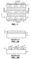
- FIG. 1is a plan view representation of a portion of a memory cell array according to one embodiment of the present invention
- FIGS. 2A and 2Bare cross-sectional views of the array of FIG. 1, taken at respective orthogonal sections A-A and B-B thereof, when in a preliminary stage of processing;
- FIGS. 3A and 3Bare cross-sectional views of the array of FIG. 1, taken at respective sections A-A and B-B thereof, at an intermediate stage in its formation;
- FIG. 4is a cross-sectional view of the array of FIG. 1, taken at section A-A thereof, when in the stage of processing shown;
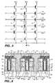
- FIG. 5is an equivalent electrical circuit of a portion of the memory cell array shown in FIGS. 1-4;
- FIG. 6is a cross-sectional view of an array according to a second embodiment of the present invention.
- FIG. 7is an equivalent electrical circuit of a portion of an array of memory cells of the type shown in FIG. 6.
- FIG. 1a plan view of the primary elements of a portion of a memory cell array is first described, and this plan view is then used as a reference for the cross-sectional views of FIGS. 2A-4, which show the array's structure at various stages of its formation.
- Conductive floating gate charge storage elements 11 - 19are regularly spaced in a two-dimensional x-y pattern across a semiconductor substrate surface, with a layer of gate dielectric therebetween.
- Control gate lines 21 - 23are elongated in the x-direction across the array and spaced apart in the orthogonal y-direction to individually extend across and be aligned with a line of floating gates, with a layer of dielectric between them.
- the lines of floating gates extending in the x-directionare referenced in this example as rows of floating gates, and the lines of floating gates extending in the y-direction are referenced as columns.
- the control gate lines 21 - 23can be, for example, word lines of the array.
- a combination of dielectric material and voidsis positioned between the rows of floating gates and the control gate lines, as best described with respect to the cross-sectional view of FIGS. 2A-4.
- FIGS. 2A and 2Bshow the result of a few initial steps in processing, in sections extending in the y-direction and x-direction, respectively, across the array of FIG. 1.
- a gate dielectric layer 25is first formed on a surface 27 of a semiconductor substrate 29 over the substrate area occupied by the array.
- the layer 25may be silicon dioxide grown on the surface 27 to a thickness of about 90 Angstroms.
- a layer of polysiliconis then deposited across the dielectric layer 25 from which the isolated floating gates are formed. The thickness of this polysilicon layer may be about 1500 Angstroms.
- the polysiliconmay be conductively doped either as part of the deposition process or after deposition by ion implantation. Initially, this polysilicon layer is separated by an etching step into strips 31 - 33 having lengths extending in the y-direction, and with widths and spacing in the x-direction that are preferably a minimum that the process being used will allow.
- a next series of stepsis illustrated by the cross-sectional views of FIGS. 3A and 3B.
- a layer 35 of dielectricis formed over the area of the array, over exposed surfaces of the doped polysilicon strips 31 - 33 and substrate surface areas therebetween.
- This dielectricis preferably formed of a composite layer of silicon dioxide, silicon nitride and silicon dioxide, commonly known as ONO. Its thickness may be about 160 Angstroms, as an example.
- a next stepis to form a second layer of doped polysilicon, or a combination of doped polysilicon and a top portion of a metal such as tungsten, over the dielectric layer 35 in the area of the array, with a thickness that may be in a range of about 3000-4000 Angstroms.
- On top of this polysilicon or polysilicon/metal layeris then formed a rather thick layer 37 of dielectric, over the area of the array, preferably silicon nitride with a thickness in a range of about 2500-3000 Angstroms.
- the combination of the layers of ONO 35 , second polysilicon or polysilicon/metal and silicon nitride 37are etched through a mask (not shown) formed on top of the layer 37 to form strips of all three layers that are elongated in the x-direction and spaced apart in the y-direction.
- the second doped polysilicon or polysilicon/metal layeris separated by this step into the control gate lines 21 - 23 .
- the widths and spacing of these stripsare also preferably made to be about a minimum that is practical with the processing being used.
- the three-layer composite stripsare so formed, they, particularly the top silicon nitride layer 37 , are used as a mask to etch away exposed portions of the first doped polysilicon layer strips 31 - 33 between them, thereby separating these first polysilicon strips into the individual floating gates 11 - 19 .
- the resultis a series of self-aligned stacks, as best illustrated in FIG. 3A, of gate dielectric 25 , one of the floating gates 12 , 15 or 18 , an inter-polysilicon layer 35 , one of conductive gate lines 21 , 22 or 23 , and a dielectric 37 .
- the widths of these composite strips in the y-directionmay be about 1400 Angstroms and the space between them in the y-direction about 1200 Angstroms, in a specific example using current state-of-the art processing technology.
- the height of the self-aligned stacks, summing the thicknesses of the individual layers given in the specific example above,is between 7250 and 8750 Angstroms.
- Spaces 41 (FIG. 3A) between these stacks in the y-directionthen have an aspect ratio (height divided by width, in cross-section) of from 6.0 to 7.3.
- the aspect ratiowill increase as a result of process improvements allowing the shrinking: of horizontal dimensions across the substrate causing the widths of the spaces 41 to be reduced without the height of the stacks forming the spaces necessarily being changed.
- the aspect ratiois also controlled, independent of the process resolution element size, by controlling the heights of the stacks without affecting operation of the resulting array, particularly by controlling the thickness of the top dielectric layer 37 or another dielectric layer that may be added on top of it. Aspect ratios of up to 12, 15 or more are contemplated.
- the spaces 41would be completely filled with silicon dioxide or other suitable solid dielectric.
- a considerable amount of efforthas been directed over the years to develop techniques for filling small spaces with silicon dioxide without leaving any voids or pockets in the solid dielectric material.
- United States patents describing this effortinclude nos. 4,892,753, 6,013,584, 6,106,678, 6,110,793 and 6,335,288.
- Technical articles on this subjectinclude Lee et al. “Dielectric Planarization Techniques For Narrow Pitch Multilevel Interconnects”, VMIC Conference , June 1987, pp. 85-92, and Qian et al., “High Density Plasma Deposition and Deep Sub-micron Gap Fill with Low Dielectric Constant SiOF Films”, California DUMIC Conference , February 1995, pp. 50-56.
- a dielectric layer 45is formed, for example by depositing silicon dioxide, which closes off the top of the spaces 41 but does not completely fill in the spaces. Rather, the dielectric is intentionally deposited in a manner to leave voids 47 .
- the voids 47occupy a majority of the width of the spaces 41 at least along the heights of the floating gates on opposite sides of the spaces, except to the extent, if any, that the dielectric formed on the bottoms of the spaces under the voids 47 is thicker than the gate dielectric layers 25 .
- a thin layer 49 of silicon dioxidemay optionally be grown over the exposed surfaces of the stacks and spaces between them.
- the dielectric layer 45can be formed with voids 47 by depositing an oxide with lower pressures and temperatures than are normally used to deposit oxide layers, such as in a low-pressure chemical-vapor-deposition (CVD) process.
- CVDchemical-vapor-deposition
- Many different combinations of starting gasses, pressures, temperatures and timesmay be used to form the layer 45 of silicon dioxide to include the voids 47 , and are usually dependent upon the particular deposition equipment being used.
- a process carried out in a plasma enhanced CVD deposition chambercauses silane (SiH 4 ) and oxygen (O 2 ) gases to react in the chamber to form the layer 45 of silicon dioxide (SiO 2 ) with the voids 47 .
- PVDPhysical vapor deposition
- the voids 47are initially filled with whatever gas or gasses are present in the deposition chamber when forming the dielectric layer 45 .
- gassestypically have a dielectric constant close to that of air, namely close to 1.0.
- these gasesare usually replaced over time with other ambient gases, such as air, in which the wafers are placed after the deposition and before the top of the layer 45 is sealed by further processing steps. The result is a desired low level of capacitive coupling between each pair of floating gates on opposite sides of one of the spaces 41 .
- the voids 47occupy as much of the width of the spaces 41 as practical and extend over as much of the vertical floating gate surface areas bordering the spaces 41 as possible.
- the width of the voids 47 in the y-directionis one-half or more of the width of the spaces 41 in the region of the opposing floating gates, such as between floating gates 12 and 15 . Even when materials having a dielectric constant less that those of silicon dioxide and silicon nitride are used, it is desirable to maintain this relative width of the voids.
- isolation between adjacent floating gatescan be further increased by use of a dielectric material for the layer 45 that has a lower dielectric constant than those of silicon dioxide or silicon nitride.
- a dielectric material for the layer 45that has a lower dielectric constant than those of silicon dioxide or silicon nitride.
- An exampleis fluorinated silicon oxide (SiOF) that may be deposited by plasma enhanced CVD or high density plasma CVD by reacting silane and one of SiF 4 , CF 4 or NF 3 within the vacuum processing chamber.
- the material SiOFhas a dielectric constant within a range of about 2.2 to 3.2.
- the voids 47contribute significantly to minimizing field coupling between adjacent rows of floating gates in a very small-scale memory cell array, and thus minimizes the influence of the level of charge of one floating gate on the state read from memory cells in adjacent rows. Isolation between memory cells along the same row (between columns of memory cells) is provided by the control gate lines extending downward between adjacent floating gates, thus shielding them from one other. This is best shown in FIG. 3B, wherein the control gate line 22 extends downward between adjacent floating gates 14 and 15 , between floating gates 15 and 16 , and so on.
- FIG. 5an equivalent circuit of a portion of a NAND array is shown in FIG. 5, with elements common to those of FIGS. 1-4 being identified by the same reference number.
- the memory cells in each columnare electrically connected together in series by implanting isolated source and drain regions (not shown) between the floating gates in the column, FIGS. 3A and 4 show cross-sectional views of one of the columns. These implants can be made at a convenient point in the processing described above, such as when in the intermediate structural state of FIGS. 3A and 3B.
- the stacks of floating and control gatescan serve as a portion of an implant mask, confining the implants in the y-direction to regions of the substrate surface 27 between them.
- the control gate lines 21 - 23are word lines of the array, each extending in the x-direction across a row of one memory cell in each of a large number of such NAND columnar series strings of memory cells.
- Each columnar string of series connected memory cells in FIG. 5includes a pair of select transistors at each end of the string, such as transistors 51 and 53 for one of the strings of FIG. 5. The string is connected through transistor 53 to a common voltage V ss such as ground, and through transistor 51 to an individual bit line BL 6 .
- control gate lines 21 - 23can be steering gates and source/drain regions can be formed in continuous lengths in the x-direction along the substrate surface 27 in spaces between the steering gates the y-direction.
- Word linescan also be added with lengths extending in the y-direction over the steering gates and coupled with certain regions of the substrate surface 27 .
- the source and drain regionsare formed in every other space between steering gates in the y-direction, these spaces then being filled with the dielectric layer 45 and voids 47 , as described.
- the word linesextend downward into these spaces and are coupled through a dielectric layer with the substrate surface 27 to form select transistors that are part of the memory cells.
- select transistorsIn such a cell, two floating gate transistors and an intermediate select transistor are connected in series in the y-direction between adjacent source/drain regions that are elongated in the x-direction.
- Floating gates 61 - 66are positioned across a surface of a semiconductor substrate with a layer 69 of gate oxide therebetween.
- Control gates 71 - 76are positioned over respective ones of the floating gates 61 - 66 with a dielectric layer 79 therebetween, and are elongated along rows of memory cells, across a large number of such columns.
- Thick dielectric regions 81are formed over the control gates. Source regions 91 and drain regions 93 , implanted into the substrate surface, alternate along the column of cells.
- a layer 83 of dielectricis deposited in the manner described above with respect to FIG. 4 for dielectric layer 45 .
- Voids 85having the same characteristics described above for the voids 47 , are formed. But rather than placing the dielectric 83 and a void 47 in each space between adjacent floating gates, they appear in every other such space over drain regions 93 . This is because the common source regions 91 are contacted by a conductor 87 that extends along the column, and thus this conductor fills those alternate spaces between side-wall spacers 89 .
- the spaces between the gate stacks that include material of the conductor 87are necessarily wider than those containing the dielectric 83 and voids 85 .
- the adjacent floating gates on opposite sides of the spaces containing the dielectric 83 and voids 85are not shielded and are close enough to have a high level of capacitive coupling if the voids 85 were not present. Since floating gates in adjacent columns can also be shielded, by extending the word lines down between them (not shown), use of the dielectric 83 and voids 85 reduces the coupling between the remaining sets of unshielded floating gates.
Landscapes
- Engineering & Computer Science (AREA)
- Physics & Mathematics (AREA)
- Condensed Matter Physics & Semiconductors (AREA)
- General Physics & Mathematics (AREA)
- Computer Hardware Design (AREA)
- Microelectronics & Electronic Packaging (AREA)
- Power Engineering (AREA)
- Manufacturing & Machinery (AREA)
- Semiconductor Memories (AREA)
- Non-Volatile Memory (AREA)
Abstract
Description
- This invention relates generally to the isolation of tightly packed elements in semiconductor structures, and, more specifically, to the electric field isolation of neighboring charge storage elements of non-volatile flash electrically erasable and programmable read-only-memory (flash EEPROM) cell arrays.[0001]
- In a first category of flash memory array architectures, memory cells are connected between adjacent bit line source and drain diffusions that extend in a column direction with control gates connected to word lines extending along rows of cells. One common memory cell has a “split-channel” between source and drain diffusions. A charge storage element of the cell is positioned over one portion of the channel and the word line (also referred to as a control gate) is positioned over the other channel portion as well as over the charge storage element. This effectively forms a cell with two transistors in series, one (the memory transistor) with a combination of the amount of charge on the charge storage element and the voltage on the word line controlling the amount of current that can flow through its portion of the channel, and the other (the select transistor) having the word line alone serving as its gate. The word line extends over a row of charge storage elements. Examples of such cells, their uses in memory systems and methods of manufacturing them are given in U.S. Pat. Nos. 5,070,032, 5,095,344, 5,315,541, 5,343,063, 5,661,053, and 6,281,075.[0002]
- A modification of this split-channel flash EEPROM cell adds a steering gate positioned between the charge storage element and the word line. Each steering gate of an array extends over one column of charge storage elements, perpendicular to the word line. The effect is to relieve the word line from having to perform two functions at the same time when reading or programming a selected cell. Those two functions are (1) to serve as a gate of a select transistor, thus requiring a proper voltage to turn the select transistor on and off, and (2) to drive the voltage of the charge storage element to a desired level through an electric field (capacitive) coupling between the word line and the charge storage element. It is often difficult to perform both of these functions in an optimum manner with a single voltage. With the addition of the steering gate, the word line need only perform function (1), while the added steering gate performs function (2). The use of steering gates in a flash EEPROM array is described, for example, in U.S. Pat. Nos. 5,313,421 and 6,222,762.[0003]
- Another type of memory array in this category that has been used commercially for many years uses an ETOX™ cell attributed to Intel Corporation. Individual memory cells are connected between a common source and shared drain lines. An early article describing this type of memory cell and array by Kynett V. N., Baker A., Fandrich M., Hockstra G., Jungroth O., Kreifels J. and Wells S. is titled “An In-system Reprogrammable 256 K CMOS Flash Memory”,[0004]ISSCC Conf. Proc., (1988) p. 132.
- In a second category of flash memory array architectures, generally referred to as NAND arrays, series strings of more than two memory cells, such as 16 or 32, are connected along with one or more select transistors between individual bit lines and a reference potential to form columns of cells. Word lines extend across cells within a large number of these columns. An individual cell within a column is read and verified during programming by causing the remaining cells in the string to be turned on hard so that the current flowing through a string is dependent upon the level of charge stored in the addressed cell. An example of a NAND architecture array and its operation as part of a memory system is found in U.S. Pat. Nos. 5,570,315, 5,774,397 and 6,046,935.[0005]
- Increasing Data Storage Density[0006]
- As in most all integrated circuit applications, the pressure to shrink the silicon substrate area required to implement some integrated circuit function also exists with flash EEPROM arrays. It is continually desired to increase the amount of digital data that can be stored in a given area of a silicon substrate, in order to increase the storage capacity of a given size memory card and other types of packages, or to both increase capacity and decrease size. One way to increase the storage density of data is to store more than one bit of data per memory cell. This is accomplished by defining more than two threshold levels as storage states for each storage element transistor, four such states (2 bits of data per storage element) now being included in commercial products. More storage states, such as 8 states (3 data bits) and 16 states (4 data bits) per storage element, are contemplated. Each storage element memory transistor has a certain total range (window) of threshold voltages in which it may practically be operated, and that range is divided into the number of states defined for it plus margins between the states to allow for them to be clearly differentiated from one another. A multiple state flash EEPROM structure and operation is described in U.S. Pat. Nos. 5,043,940 and 5,172,338, for example.[0007]
- Another type of memory cell includes two storage elements that may also be operated in multiple states on each storage element. In this type of cell, two storage elements are included over its channel between source and drain diffusions with a select transistor in between them. A steering gate is included along each column of storage elements and a word line is provided thereover along each row of storage elements. When accessing a given storage element for reading or programming, the steering gate over the other storage element of the cell containing the storage element of interest is raised sufficiently high to turn on the channel under the other storage element no matter what charge level exists on it. This effectively eliminates the other storage element as a factor in reading or programming the storage element of interest in the same memory cell. For example, the amount of current flowing through the cell, which can be used to read its state, is then a function of the amount of charge on the storage element of interest but not of the other storage element in the same cell. Examples of this cell array architecture and operating techniques are described in U.S. Pat. Nos. 5,712,180, 6,103,573 and 6,151,248.[0008]
- Charge Storage Elements[0009]
- The charge storage elements of current flash EEPROM arrays and discussed in the foregoing referenced patents and articles are most commonly electrically conductive floating gates, typically formed from doped polysilicon material. Another type of memory cell useful in flash EEPROM systems utilizes a non-conductive dielectric material in place of a conductive floating gate to store charge in a non-volatile manner. Such a cell is described in an article by Chan et al., “A True Single-Transistor Oxide-Nitride-Oxide EEPROM Device,” IEEE Electron Device Letters, Vol. EDL-8, No. 3, March 1987, pp. 93-95. A triple layer dielectric formed of silicon oxide, silicon nitride and silicon oxide (“ONO”) is sandwiched between a conductive control gate and a surface of a semi-conductive substrate above the memory cell channel. The cell is programmed by injecting electrons from the cell channel into the nitride, where they are trapped and stored in a limited region. This stored charge then changes the threshold voltage of a portion of the channel of the cell in a manner that is detectable. The cell is erased by injecting hot holes into the nitride. See also Nozaki et al., “A 1-Mb EEPROM with MONOS Memory Cell for Semiconductor Disk Application,”[0010]IEEE Journal of Solid-State Circuits, Vol. 26, No. 4, April 1991, pp. 497-501, which describes a similar cell in a split-gate configuration where a doped polysilicon gate extends over a portion of the memory cell channel to form a separate select transistor.
- Another approach to storing two bits in each cell utilizing a dielectric storage medium has been described by Eitan et al., “NROM: A Novel Localized Trapping, 2-Bit Nonvolatile Memory Cell,”[0011]IEEE Electron Device Letters, vol. 21, no. 11, November 2000, pp. 543-545. An ONO dielectric layer extends across the channel between source and drain diffusions. The charge for one data bit is localized in the dielectric layer adjacent to the drain, and the charge for the other data bit is localized in the dielectric layer adjacent to the source. Multi-state data storage is obtained by separately reading binary states of the spatially separated charge storage regions within the dielectric.
- The use of dielectric charge storage media in NOR, NAND and other flash EEPROM architectures is further described in pending U.S. application Ser. No. 10/280,352, filed Oct. 25, 2002 by Harari et al., and entitled “Multi-State Non-Volatile Integrated Circuit Memory Systems that Employ Dielectric Storage Elements”.[0012]
- Interaction Between Neighboring Charge Storage Elements[0013]
- As the number of states stored in each memory cell increases, the tolerance of any shifts in the programmed charge level on the storage elements decreases. Since the ranges of charge designated for each storage state must necessarily be made narrower and placed closer together as the number of states stored on each memory cell storage element increases, the programming must be performed with an increased degree of precision and the extent of any post-programming shifts in the stored charge levels that can be tolerated, either actual or apparent shifts, is reduced. Actual disturbs to the charge stored in one cell can be created when programming and reading that cell, and when reading, programming and erasing other cells that have some degree of electrical coupling with that cell, such as those in the same column or row, and those sharing a line or node.[0014]
- In addition, apparent shifts in the stored charge levels occur because of field coupling between storage elements. The degree of this coupling necessarily increases as the spaces between memory cell storage elements are decreased, which is occurring as the result of improvements of integrated circuit manufacturing techniques. The problem occurs most pronouncedly between two groups of adjacent cells that have been programmed at different times. One group of cells is programmed to add a level of charge to their storage elements that corresponds to one set of data. After the second group of cells is programmed with a second set of data, the charge levels read from the storage elements of the first group of cells often appear to be different than programmed because of the effect of the charge on the second group of storage elements being capacitively coupled with that the first group. This is known as the “Yupin” effect, and is described in U.S. Pat. No. 5,867,429.[0015]
- The effect of this parasitic capacitance between storage elements can be compensated by taking into account the effect of the charge on the second group of storage elements when reading that of the first group. Also, the effect may be reduced by physically isolating the two groups of storage elements from each other, such as by placing a conductive shield between the two groups. One way in which such shielding has been accomplished is to extend control gate lines, which run across either rows or columns of floating gates, downward between the floating gates. Further, it has been suggested that the parasitic capacitance between floating gates may be reduced by positioning a dielectric material between them, either in a solid or a non-solid form, which has a very low dielectric constant, but of course not less than 1.0. Another technique to reduce coupling between floating gates is to make them very thin so that their opposing surface areas are small.[0016]
- Isolation between adjacent charge storage elements is provided by forming a dielectric between them that contains a void extending a major part of the distance between the elements instead of the usual technique of making the dielectric solid throughout the entire space between charge storage elements. The void will usually contain the gas present in the processing chamber when the dielectric is formed. Such a gas has a dielectric constant of 1.0 or only a small amount above 1.0, depending upon its exact composition. This is considerably less than that of commonly used dielectric materials such as silicon dioxide, with a dielectric constant of about 4.0, depending upon the exact composition and method of formation, and silicon nitride with a dielectric constant of about 7.5. A significant reduction in the coupling between adjacent charge storage elements is thus achieved.[0017]
- In one embodiment, this isolation is formed in spaces between floating gates at the bottom of stacks of layers having a height of five, eight or more times the width of the spaces between the stacks. The other layers in the stacks usually contain at least one dielectric and a conductive control gate line. This 5:1, 8:1 or more cross-sectional aspect ratio of the spaces between the stacks allows a dielectric to be formed that extends downward into the spaces along sidewalls of the stacks but not filling the bottom segments of the spaces between the charge storage elements. Top portions of the spaces are filled with the dielectric, however, thereby leaving large voids sealed in the dielectric between the charge storage elements.[0018]
- These isolation techniques are applied to a wide variety of non-volatile memory cell arrays, such as those within the two categories described in the Background. In a specific NAND array, for example, control gate (word) lines extend over rows of floating gates and down between them, thereby providing shielding along the rows as well as desirably increasing the coupling between each of the word lines and the floating gates in its row. The dielectric with voids is then formed between the rows in order to reduce capacitive coupling between floating gates along the columns (i.e., along NAND strings of floating gate transistors). Another example use of the isolation techniques herein is with an ETOX™ array having alternate source and drain implants in one direction across the array, between which the individual charge floating gates are positioned. Although a conductor usually extends between the floating gates to contact every other implant region along each row of memory cells, and thus provide some shielding between the floating gates on either side of the conductor, the alternate spaces between floating gates over the remaining implant regions are very small. The dielectric with voids is used in these small spaces instead of the usual solid dielectric such as silicon dioxide.[0019]
- Additional aspects, advantages and features of the present invention are included in the following description of exemplary examples thereof, which description should be taken in conjunction with the accompanying drawings.[0020]
- FIG. 1 is a plan view representation of a portion of a memory cell array according to one embodiment of the present invention;[0021]
- FIGS. 2A and 2B are cross-sectional views of the array of FIG. 1, taken at respective orthogonal sections A-A and B-B thereof, when in a preliminary stage of processing;[0022]
- FIGS. 3A and 3B are cross-sectional views of the array of FIG. 1, taken at respective sections A-A and B-B thereof, at an intermediate stage in its formation;[0023]
- FIG. 4 is a cross-sectional view of the array of FIG. 1, taken at section A-A thereof, when in the stage of processing shown;[0024]
- FIG. 5 is an equivalent electrical circuit of a portion of the memory cell array shown in FIGS. 1-4;[0025]
- FIG. 6 is a cross-sectional view of an array according to a second embodiment of the present invention; and[0026]
- FIG. 7 is an equivalent electrical circuit of a portion of an array of memory cells of the type shown in FIG. 6.[0027]
- Referring initially to FIG. 1, a plan view of the primary elements of a portion of a memory cell array is first described, and this plan view is then used as a reference for the cross-sectional views of FIGS. 2A-4, which show the array's structure at various stages of its formation. Conductive floating gate charge storage elements[0028]11-19 are regularly spaced in a two-dimensional x-y pattern across a semiconductor substrate surface, with a layer of gate dielectric therebetween. Control gate lines21-23 are elongated in the x-direction across the array and spaced apart in the orthogonal y-direction to individually extend across and be aligned with a line of floating gates, with a layer of dielectric between them. The lines of floating gates extending in the x-direction are referenced in this example as rows of floating gates, and the lines of floating gates extending in the y-direction are referenced as columns. The control gate lines21-23 can be, for example, word lines of the array. A combination of dielectric material and voids is positioned between the rows of floating gates and the control gate lines, as best described with respect to the cross-sectional view of FIGS. 2A-4.
- FIGS. 2A and 2B show the result of a few initial steps in processing, in sections extending in the y-direction and x-direction, respectively, across the array of FIG. 1. A[0029]
gate dielectric layer 25 is first formed on asurface 27 of asemiconductor substrate 29 over the substrate area occupied by the array. Thelayer 25 may be silicon dioxide grown on thesurface 27 to a thickness of about 90 Angstroms. A layer of polysilicon is then deposited across thedielectric layer 25 from which the isolated floating gates are formed. The thickness of this polysilicon layer may be about 1500 Angstroms. The polysilicon may be conductively doped either as part of the deposition process or after deposition by ion implantation. Initially, this polysilicon layer is separated by an etching step into strips31-33 having lengths extending in the y-direction, and with widths and spacing in the x-direction that are preferably a minimum that the process being used will allow. - A next series of steps is illustrated by the cross-sectional views of FIGS. 3A and 3B. A[0030]
layer 35 of dielectric is formed over the area of the array, over exposed surfaces of the doped polysilicon strips31-33 and substrate surface areas therebetween. This dielectric is preferably formed of a composite layer of silicon dioxide, silicon nitride and silicon dioxide, commonly known as ONO. Its thickness may be about 160 Angstroms, as an example. A next step is to form a second layer of doped polysilicon, or a combination of doped polysilicon and a top portion of a metal such as tungsten, over thedielectric layer 35 in the area of the array, with a thickness that may be in a range of about 3000-4000 Angstroms. On top of this polysilicon or polysilicon/metal layer is then formed a ratherthick layer 37 of dielectric, over the area of the array, preferably silicon nitride with a thickness in a range of about 2500-3000 Angstroms. - Next, the combination of the layers of[0031]
ONO 35, second polysilicon or polysilicon/metal andsilicon nitride 37 are etched through a mask (not shown) formed on top of thelayer 37 to form strips of all three layers that are elongated in the x-direction and spaced apart in the y-direction. The second doped polysilicon or polysilicon/metal layer is separated by this step into the control gate lines21-23. The widths and spacing of these strips are also preferably made to be about a minimum that is practical with the processing being used. After the three-layer composite strips are so formed, they, particularly the topsilicon nitride layer 37, are used as a mask to etch away exposed portions of the first doped polysilicon layer strips31-33 between them, thereby separating these first polysilicon strips into the individual floating gates11-19. The result is a series of self-aligned stacks, as best illustrated in FIG. 3A, ofgate dielectric 25, one of the floatinggates inter-polysilicon layer 35, one ofconductive gate lines - The widths of these composite strips in the y-direction may be about 1400 Angstroms and the space between them in the y-direction about 1200 Angstroms, in a specific example using current state-of-the art processing technology. The height of the self-aligned stacks, summing the thicknesses of the individual layers given in the specific example above, is between 7250 and 8750 Angstroms. Spaces[0032]41 (FIG. 3A) between these stacks in the y-direction then have an aspect ratio (height divided by width, in cross-section) of from 6.0 to 7.3. The aspect ratio will increase as a result of process improvements allowing the shrinking: of horizontal dimensions across the substrate causing the widths of the
spaces 41 to be reduced without the height of the stacks forming the spaces necessarily being changed. The aspect ratio is also controlled, independent of the process resolution element size, by controlling the heights of the stacks without affecting operation of the resulting array, particularly by controlling the thickness of thetop dielectric layer 37 or another dielectric layer that may be added on top of it. Aspect ratios of up to 12, 15 or more are contemplated. - Typically, the[0033]
spaces 41 would be completely filled with silicon dioxide or other suitable solid dielectric. A considerable amount of effort has been directed over the years to develop techniques for filling small spaces with silicon dioxide without leaving any voids or pockets in the solid dielectric material. United States patents describing this effort include nos. 4,892,753, 6,013,584, 6,106,678, 6,110,793 and 6,335,288. Technical articles on this subject include Lee et al. “Dielectric Planarization Techniques For Narrow Pitch Multilevel Interconnects”,VMIC Conference, June 1987, pp. 85-92, and Qian et al., “High Density Plasma Deposition and Deep Sub-micron Gap Fill with Low Dielectric Constant SiOF Films”,California DUMIC Conference, February 1995, pp. 50-56. - But in the process being described, as illustrated in the cross-sectional view of FIG. 4, a[0034]
dielectric layer 45 is formed, for example by depositing silicon dioxide, which closes off the top of thespaces 41 but does not completely fill in the spaces. Rather, the dielectric is intentionally deposited in a manner to leavevoids 47. Thevoids 47 occupy a majority of the width of thespaces 41 at least along the heights of the floating gates on opposite sides of the spaces, except to the extent, if any, that the dielectric formed on the bottoms of the spaces under thevoids 47 is thicker than the gate dielectric layers25. Prior to depositing thedielectric layer 45, athin layer 49 of silicon dioxide may optionally be grown over the exposed surfaces of the stacks and spaces between them. - The[0035]
dielectric layer 45 can be formed withvoids 47 by depositing an oxide with lower pressures and temperatures than are normally used to deposit oxide layers, such as in a low-pressure chemical-vapor-deposition (CVD) process. Many different combinations of starting gasses, pressures, temperatures and times may be used to form thelayer 45 of silicon dioxide to include thevoids 47, and are usually dependent upon the particular deposition equipment being used. By way of illustration, a process carried out in a plasma enhanced CVD deposition chamber causes silane (SiH4) and oxygen (O2) gases to react in the chamber to form thelayer 45 of silicon dioxide (SiO2) with thevoids 47. Physical vapor deposition (PVD) techniques can alternatively be employed, including sputtering within a vacuum chamber from of a target of silicon dioxide, to deposit a silicon dioxide film, or a target of silicon nitride (Si3Ni4) to deposit a silicon nitride film. - The[0036]
voids 47 are initially filled with whatever gas or gasses are present in the deposition chamber when forming thedielectric layer 45. Such gasses typically have a dielectric constant close to that of air, namely close to 1.0. But since the material of thelayer 45 is generally porous, these gases are usually replaced over time with other ambient gases, such as air, in which the wafers are placed after the deposition and before the top of thelayer 45 is sealed by further processing steps. The result is a desired low level of capacitive coupling between each pair of floating gates on opposite sides of one of thespaces 41. Since silicon dioxide typically has a dielectric constant of about 4.0 and silicon nitride around 7.5, use of either of these materials makes it desirable that thevoids 47 occupy as much of the width of thespaces 41 as practical and extend over as much of the vertical floating gate surface areas bordering thespaces 41 as possible. In FIG. 4, the width of thevoids 47 in the y-direction is one-half or more of the width of thespaces 41 in the region of the opposing floating gates, such as between floatinggates - In addition to forming the[0037]
voids 47 as part of the process of depositing thedielectric layer 45, isolation between adjacent floating gates can be further increased by use of a dielectric material for thelayer 45 that has a lower dielectric constant than those of silicon dioxide or silicon nitride. An example is fluorinated silicon oxide (SiOF) that may be deposited by plasma enhanced CVD or high density plasma CVD by reacting silane and one of SiF4, CF4or NF3within the vacuum processing chamber. The material SiOF has a dielectric constant within a range of about 2.2 to 3.2. - In the exemplary memory cell array of FIGS. 1-4, the[0038]
voids 47 contribute significantly to minimizing field coupling between adjacent rows of floating gates in a very small-scale memory cell array, and thus minimizes the influence of the level of charge of one floating gate on the state read from memory cells in adjacent rows. Isolation between memory cells along the same row (between columns of memory cells) is provided by the control gate lines extending downward between adjacent floating gates, thus shielding them from one other. This is best shown in FIG. 3B, wherein thecontrol gate line 22 extends downward between adjacent floatinggates gates - The techniques described herein for isolating adjacent floating gates can be applied to a variety of memory cell array architectures. For example, an equivalent circuit of a portion of a NAND array is shown in FIG. 5, with elements common to those of FIGS. 1-4 being identified by the same reference number. In this case, the memory cells in each column are electrically connected together in series by implanting isolated source and drain regions (not shown) between the floating gates in the column, FIGS. 3A and 4 show cross-sectional views of one of the columns. These implants can be made at a convenient point in the processing described above, such as when in the intermediate structural state of FIGS. 3A and 3B. The stacks of floating and control gates can serve as a portion of an implant mask, confining the implants in the y-direction to regions of the[0039]
substrate surface 27 between them. In the case of a NAND array, the control gate lines21-23 are word lines of the array, each extending in the x-direction across a row of one memory cell in each of a large number of such NAND columnar series strings of memory cells. Each columnar string of series connected memory cells in FIG. 5 includes a pair of select transistors at each end of the string, such astransistors transistor 53 to a common voltage Vsssuch as ground, and throughtransistor 51 to an individual bit line BL6. - The same techniques are used to advantage in the first category of flash memory cell arrays discussed above in the Background. For example, the control gate lines[0040]21-23 can be steering gates and source/drain regions can be formed in continuous lengths in the x-direction along the
substrate surface 27 in spaces between the steering gates the y-direction. Word lines can also be added with lengths extending in the y-direction over the steering gates and coupled with certain regions of thesubstrate surface 27. In a specific configuration, the source and drain regions are formed in every other space between steering gates in the y-direction, these spaces then being filled with thedielectric layer 45 and voids47, as described. In the remaining alternate spaces between steering gates, the word lines extend downward into these spaces and are coupled through a dielectric layer with thesubstrate surface 27 to form select transistors that are part of the memory cells. In such a cell, two floating gate transistors and an intermediate select transistor are connected in series in the y-direction between adjacent source/drain regions that are elongated in the x-direction. - Application of the isolation techniques of the present invention to an ETOX™ memory cell array is illustrated in the cross-sectional view in FIG. 6 along a column of a few memory cells. Floating gates[0041]61-66 are positioned across a surface of a semiconductor substrate with a
layer 69 of gate oxide therebetween. Control gates71-76, in this case word lines, are positioned over respective ones of the floating gates61-66 with adielectric layer 79 therebetween, and are elongated along rows of memory cells, across a large number of such columns. Thickdielectric regions 81 are formed over the control gates.Source regions 91 anddrain regions 93, implanted into the substrate surface, alternate along the column of cells. - At a point in the processing when the stacks of floating gates, control gates and associated dielectric regions are formed, a[0042]
layer 83 of dielectric is deposited in the manner described above with respect to FIG. 4 fordielectric layer 45.Voids 85, having the same characteristics described above for thevoids 47, are formed. But rather than placing the dielectric83 and a void47 in each space between adjacent floating gates, they appear in every other such space overdrain regions 93. This is because thecommon source regions 91 are contacted by aconductor 87 that extends along the column, and thus this conductor fills those alternate spaces between side-wall spacers 89. The spaces between the gate stacks that include material of theconductor 87 are necessarily wider than those containing the dielectric83 and voids85. The adjacent floating gates on opposite sides of the spaces containing the dielectric83 and voids85 are not shielded and are close enough to have a high level of capacitive coupling if thevoids 85 were not present. Since floating gates in adjacent columns can also be shielded, by extending the word lines down between them (not shown), use of the dielectric83 and voids85 reduces the coupling between the remaining sets of unshielded floating gates. - Although the various aspects of the present invention have been described with respect to exemplary embodiments thereof, it will be understood that the present invention is entitled to protection within the full scope of the appended claims. Further, each of the patents, patent applications, articles and other publications referenced in this document are expressly incorporated herein in their entirety.[0043]
Claims (9)
Priority Applications (8)
| Application Number | Priority Date | Filing Date | Title |
|---|---|---|---|
| US10/443,502US7045849B2 (en) | 2003-05-21 | 2003-05-21 | Use of voids between elements in semiconductor structures for isolation |
| CNB2004800139911ACN100428440C (en) | 2003-05-21 | 2004-05-03 | The use of voids between elements in semiconductor structures as isolation |
| JP2006532783AJP2007501531A (en) | 2003-05-21 | 2004-05-03 | Use of voids between elements in semiconductor structures for element isolation. |
| PCT/US2004/013986WO2004107352A2 (en) | 2003-05-21 | 2004-05-03 | Use of voids between elements in semiconductor structures for isolation |
| EP04751389AEP1625616A2 (en) | 2003-05-21 | 2004-05-03 | Use of voids between elements in semiconductor structures for isolation |
| KR1020057022214AKR20060017803A (en) | 2003-05-21 | 2004-05-03 | Method of using voids between elements of semiconductor structures for insulation |
| TW093114160ATWI267943B (en) | 2003-05-21 | 2004-05-19 | Use of voids between elements in semiconductor structures for isolation |
| US11/210,218US7569465B2 (en) | 2003-05-21 | 2005-08-22 | Use of voids between elements in semiconductor structures for isolation |
Applications Claiming Priority (1)
| Application Number | Priority Date | Filing Date | Title |
|---|---|---|---|
| US10/443,502US7045849B2 (en) | 2003-05-21 | 2003-05-21 | Use of voids between elements in semiconductor structures for isolation |
Related Child Applications (1)
| Application Number | Title | Priority Date | Filing Date |
|---|---|---|---|
| US11/210,218DivisionUS7569465B2 (en) | 2003-05-21 | 2005-08-22 | Use of voids between elements in semiconductor structures for isolation |
Publications (2)
| Publication Number | Publication Date |
|---|---|
| US20040232496A1true US20040232496A1 (en) | 2004-11-25 |
| US7045849B2 US7045849B2 (en) | 2006-05-16 |
Family
ID=33450432
Family Applications (2)
| Application Number | Title | Priority Date | Filing Date |
|---|---|---|---|
| US10/443,502Expired - LifetimeUS7045849B2 (en) | 2003-05-21 | 2003-05-21 | Use of voids between elements in semiconductor structures for isolation |
| US11/210,218Expired - LifetimeUS7569465B2 (en) | 2003-05-21 | 2005-08-22 | Use of voids between elements in semiconductor structures for isolation |
Family Applications After (1)
| Application Number | Title | Priority Date | Filing Date |
|---|---|---|---|
| US11/210,218Expired - LifetimeUS7569465B2 (en) | 2003-05-21 | 2005-08-22 | Use of voids between elements in semiconductor structures for isolation |
Country Status (7)
| Country | Link |
|---|---|
| US (2) | US7045849B2 (en) |
| EP (1) | EP1625616A2 (en) |
| JP (1) | JP2007501531A (en) |
| KR (1) | KR20060017803A (en) |
| CN (1) | CN100428440C (en) |
| TW (1) | TWI267943B (en) |
| WO (1) | WO2004107352A2 (en) |
Cited By (40)
| Publication number | Priority date | Publication date | Assignee | Title |
|---|---|---|---|---|
| EP1672646A1 (en)* | 2004-12-14 | 2006-06-21 | STMicroelectronics S.r.l. | Electronic memory device having high integration density non volatile memory cells and a reduced capacitive coupling |
| EP1672645A1 (en) | 2004-12-14 | 2006-06-21 | STMicroelectronics S.r.l. | Electronic memory device having high density non volatile memory cells and a reduced capacitive interference cell-to-cell |
| DE102005010821A1 (en)* | 2005-03-07 | 2006-09-14 | Technische Universität Berlin | Method for producing a component |
| US20060231884A1 (en)* | 2005-04-15 | 2006-10-19 | Renesas Technology Corp. | Nonvolatile semiconductor device and method of manufacturing nonvolatile semiconductor device |
| US20070018215A1 (en)* | 2005-07-19 | 2007-01-25 | Micron Technology, Inc. | Semiconductor constructions, memory arrays, electronic systems, and methods of forming semiconductor constructions |
| US20070045769A1 (en)* | 2005-09-01 | 2007-03-01 | Micron Technology, Inc. | Semiconductor constructions, memory arrays, electronic systems, and methods of forming semiconductor constructions |
| US20070063257A1 (en)* | 2005-09-22 | 2007-03-22 | Samsung Electronics Co., Ltd. | Nonvolatile memory devices including high-voltage MOS transistors with floated drain-side auxiliary gates and methods of fabricating the same |
| US20070096202A1 (en)* | 2005-10-31 | 2007-05-03 | Samsung Electronics Co., Ltd. | Semiconductor device and method for fabricating the same |
| EP1804293A1 (en)* | 2005-12-30 | 2007-07-04 | STMicroelectronics S.r.l. | Process for manufacturing a non volatile memory electronic device |
| US20070212874A1 (en)* | 2006-03-08 | 2007-09-13 | Micron Technology, Inc. | Method for filling shallow isolation trenches and other recesses during the formation of a semiconductor device and electronic systems including the semiconductor device |
| US20070238295A1 (en)* | 2006-04-11 | 2007-10-11 | Micron Technology, Inc. | Methods of forming semiconductor constructions |
| US20070284648A1 (en)* | 2006-03-17 | 2007-12-13 | Park Yoon-Dong | Non-volatile memory device and method of manufacturing the same |
| US20080265377A1 (en)* | 2007-04-30 | 2008-10-30 | International Business Machines Corporation | Air gap with selective pinchoff using an anti-nucleation layer |
| US20090212352A1 (en)* | 2008-02-26 | 2009-08-27 | Kenji Aoyama | Semiconductor memory device and method for manufacturing the same |
| US20090218614A1 (en)* | 2008-03-03 | 2009-09-03 | Kenji Aoyama | Semiconductor storage device and method for manufacturing the same |
| US20090253255A1 (en)* | 2006-11-15 | 2009-10-08 | Kim Won-Joo | Semiconductor device having a pair of fins and method of manufacturing the same |
| US20100072538A1 (en)* | 2008-09-25 | 2010-03-25 | Kabushiki Kaisha Toshiba | Nonvolatile semiconductor memory device and method of manufacturing the same |
| US20100207193A1 (en)* | 2009-02-16 | 2010-08-19 | Kabushiki Kaisha Toshiba | Non-volatile semiconductor storage device and method of manufacturing the same |
| US20110163367A1 (en)* | 2005-10-31 | 2011-07-07 | Dae-Woong Kang | Semiconductor Devices Comprising a Plurality of Gate Structures |
| US20110266689A1 (en)* | 2009-05-06 | 2011-11-03 | Micron Technology, Inc. | Methods Of Forming A Plurality Of Conductive Lines In The Fabrication Of Integrated Circuitry, Methods Of Forming An Array Of Conductive Lines, And Integrated Circuitry |
| US20120126306A1 (en)* | 2010-11-18 | 2012-05-24 | Kabushiki Kaisha Toshiba | Nonvolatile semiconductor memory device and manufacturing method of nonvolatile semiconductor memory device |
| US20120126303A1 (en)* | 2010-11-18 | 2012-05-24 | Kabushiki Kaisha Toshiba | Nonvolatile semiconductor memory device and method for manufacturing nonvolatile semiconductor memory device |
| US20120132985A1 (en)* | 2010-11-30 | 2012-05-31 | Kabushiki Kaisha Toshiba | Non-volatile semiconductor memory device and method of manufacturing non-volatile semiconductor memory device |
| US20130020708A1 (en)* | 2011-07-19 | 2013-01-24 | SanDisk Technologies, Inc | Copper Interconnects Separated by Air Gaps and Method of Making Thereof |
| CN103390560A (en)* | 2013-07-25 | 2013-11-13 | 上海宏力半导体制造有限公司 | Forming method of semiconductor device and semiconductor device |
| US8637930B2 (en)* | 2011-10-13 | 2014-01-28 | International Business Machines Company | FinFET parasitic capacitance reduction using air gap |
| US20140061759A1 (en)* | 2012-08-30 | 2014-03-06 | SK Hynix Inc. | Nonvolatile memory device and method for fabricating the same |
| CN103779401A (en)* | 2012-10-26 | 2014-05-07 | 旺宏电子股份有限公司 | Gate structure and manufacturing method thereof |
| US20150035068A1 (en)* | 2012-09-14 | 2015-02-05 | Macronix International Co., Ltd. | Airgap structure and method of manufacturing thereof |
| US20160079263A1 (en)* | 2014-09-11 | 2016-03-17 | Kabushiki Kaisha Toshiba | Semiconductor memory device and method for manufacturing the same |
| US20160133671A1 (en)* | 2014-11-07 | 2016-05-12 | Micron Technology, Inc. | Cross-point memory and methods for fabrication of same |
| CN108054153A (en)* | 2012-09-14 | 2018-05-18 | 三星电子株式会社 | Utilize the semiconductor devices and its manufacturing method of airspace separation conductive structure |
| US20210265365A1 (en)* | 2017-08-11 | 2021-08-26 | Micron Technology, Inc. | Void formation in charge trap structures |
| US20220157647A1 (en)* | 2016-05-31 | 2022-05-19 | Taiwan Semiconductor Manufacturing Company, Ltd. | Semiconductor structure and manufacturing method thereof |
| US20220278275A1 (en)* | 2019-03-05 | 2022-09-01 | SK Hynix Inc. | Electronic device and method for fabricating the same |
| CN115440731A (en)* | 2022-08-24 | 2022-12-06 | 芯盟科技有限公司 | Semiconductor device and manufacturing method thereof |
| US20230087442A1 (en)* | 2021-09-23 | 2023-03-23 | Applied Materials, Inc. | Multi process air gap formation |
| US11765903B2 (en) | 2017-08-11 | 2023-09-19 | Micron Technology, Inc. | Charge trap structure with barrier to blocking region |
| US11923407B2 (en) | 2017-08-11 | 2024-03-05 | Micron Technology, Inc. | Memory device including voids between control gates |
| US11943924B2 (en) | 2017-08-11 | 2024-03-26 | Micron Technology, Inc. | Void formation for charge trap structures |
Families Citing this family (85)
| Publication number | Priority date | Publication date | Assignee | Title |
|---|---|---|---|---|
| US7045849B2 (en)* | 2003-05-21 | 2006-05-16 | Sandisk Corporation | Use of voids between elements in semiconductor structures for isolation |
| US7078742B2 (en) | 2003-07-25 | 2006-07-18 | Taiwan Semiconductor Manufacturing Co., Ltd. | Strained-channel semiconductor structure and method of fabricating the same |
| US6936881B2 (en)* | 2003-07-25 | 2005-08-30 | Taiwan Semiconductor Manufacturing Company, Ltd. | Capacitor that includes high permittivity capacitor dielectric |
| US7101742B2 (en)* | 2003-08-12 | 2006-09-05 | Taiwan Semiconductor Manufacturing Company, Ltd. | Strained channel complementary field-effect transistors and methods of manufacture |
| US7112495B2 (en)* | 2003-08-15 | 2006-09-26 | Taiwan Semiconductor Manufacturing Company, Ltd. | Structure and method of a strained channel transistor and a second semiconductor component in an integrated circuit |
| US7071052B2 (en)* | 2003-08-18 | 2006-07-04 | Taiwan Semiconductor Manufacturing Company, Ltd. | Resistor with reduced leakage |
| US7888201B2 (en) | 2003-11-04 | 2011-02-15 | Taiwan Semiconductor Manufacturing Company, Ltd. | Semiconductor-on-insulator SRAM configured using partially-depleted and fully-depleted transistors |
| US7638850B2 (en)* | 2004-10-14 | 2009-12-29 | Saifun Semiconductors Ltd. | Non-volatile memory structure and method of fabrication |
| JP2006228893A (en)* | 2005-02-16 | 2006-08-31 | Renesas Technology Corp | Semiconductor device and its manufacturing method |
| KR100693253B1 (en)* | 2005-07-06 | 2007-03-13 | 삼성전자주식회사 | Semiconductor device and manufacturing method |
| US7307027B1 (en)* | 2005-08-11 | 2007-12-11 | Advanced Micro Devices, Inc. | Void free interlayer dielectric |
| JP4731262B2 (en)* | 2005-09-22 | 2011-07-20 | ルネサスエレクトロニクス株式会社 | Nonvolatile semiconductor memory device and method of manufacturing nonvolatile semiconductor memory device |
| US7615448B2 (en)* | 2005-12-06 | 2009-11-10 | Sandisk Corporation | Method of forming low resistance void-free contacts |
| US7737483B2 (en)* | 2005-12-06 | 2010-06-15 | Sandisk Corporation | Low resistance void-free contacts |
| CN101017783B (en)* | 2006-02-06 | 2013-06-19 | 中芯国际集成电路制造(上海)有限公司 | Method for making the separated dual-bar field effect transistor |
| US7984408B2 (en)* | 2006-04-21 | 2011-07-19 | International Business Machines Corporation | Structures incorporating semiconductor device structures with reduced junction capacitance and drain induced barrier lowering |
| US7659178B2 (en)* | 2006-04-21 | 2010-02-09 | International Business Machines Corporation | Semiconductor device structures with reduced junction capacitance and drain induced barrier lowering and methods for fabricating such device structures and for fabricating a semiconductor-on-insulator substrate |
| KR100777016B1 (en)* | 2006-06-20 | 2007-11-16 | 재단법인서울대학교산학협력재단 | NAND flash memory array with columnar structure and manufacturing method |
| JP4827639B2 (en)* | 2006-07-12 | 2011-11-30 | ルネサスエレクトロニクス株式会社 | Semiconductor device and manufacturing method thereof |
| KR100875055B1 (en)* | 2006-07-14 | 2008-12-19 | 주식회사 하이닉스반도체 | Manufacturing Method of NAND Flash Memory Device |
| KR100880310B1 (en)* | 2006-09-06 | 2009-01-28 | 주식회사 하이닉스반도체 | Manufacturing method of semiconductor device |
| JP4364225B2 (en)* | 2006-09-15 | 2009-11-11 | 株式会社東芝 | Semiconductor device and manufacturing method thereof |
| US8558278B2 (en)* | 2007-01-16 | 2013-10-15 | Taiwan Semiconductor Manufacturing Company, Ltd. | Strained transistor with optimized drive current and method of forming |
| US7948021B2 (en)* | 2007-04-27 | 2011-05-24 | Kabushiki Kaisha Toshiba | Semiconductor memory device and method of fabricating the same |
| JP2008283095A (en)* | 2007-05-14 | 2008-11-20 | Toshiba Corp | Nonvolatile semiconductor memory device and manufacturing method thereof |
| JP2009010088A (en) | 2007-06-27 | 2009-01-15 | Toshiba Corp | Semiconductor device and manufacturing method thereof |
| KR101010798B1 (en)* | 2007-07-18 | 2011-01-25 | 주식회사 하이닉스반도체 | Manufacturing Method of Flash Memory Device |
| KR100843044B1 (en)* | 2007-08-20 | 2008-07-01 | 주식회사 하이닉스반도체 | Manufacturing method of semiconductor device |
| KR20090067453A (en)* | 2007-12-21 | 2009-06-25 | 주식회사 동부하이텍 | Semiconductor element and manufacturing method thereof |
| JP2009194244A (en) | 2008-02-15 | 2009-08-27 | Toshiba Corp | Semiconductor memory device and manufacturing method thereof |
| JP4703669B2 (en)* | 2008-02-18 | 2011-06-15 | 株式会社東芝 | Semiconductor memory device and manufacturing method thereof |
| US7943961B2 (en)* | 2008-03-13 | 2011-05-17 | Taiwan Semiconductor Manufacturing Company, Ltd. | Strain bars in stressed layers of MOS devices |
| US7859040B2 (en)* | 2008-07-10 | 2010-12-28 | Seagate Technology Llc | Non-volatile memory |
| JP4956500B2 (en) | 2008-07-22 | 2012-06-20 | 株式会社東芝 | Semiconductor memory device and manufacturing method thereof |
| US7808051B2 (en)* | 2008-09-29 | 2010-10-05 | Taiwan Semiconductor Manufacturing Company, Ltd. | Standard cell without OD space effect in Y-direction |
| JP4923078B2 (en)* | 2009-03-23 | 2012-04-25 | 株式会社東芝 | Semiconductor memory device and method of manufacturing the semiconductor memory device |
| US8189410B1 (en) | 2010-04-27 | 2012-05-29 | Bruce Lee Morton | Memory device and method thereof |
| US9099169B1 (en) | 2010-04-27 | 2015-08-04 | Tagmatech, Llc | Memory device and method thereof |
| US8339873B1 (en) | 2010-04-27 | 2012-12-25 | Bruce Lee Morton | Memory device and method thereof |
| US8455940B2 (en)* | 2010-05-24 | 2013-06-04 | Samsung Electronics Co., Ltd. | Nonvolatile memory device, method of manufacturing the nonvolatile memory device, and memory module and system including the nonvolatile memory device |
| TWI539172B (en)* | 2010-06-30 | 2016-06-21 | 生命技術公司 | Methods and apparatus for testing isfet arrays |
| JP2013540259A (en) | 2010-06-30 | 2013-10-31 | ライフ テクノロジーズ コーポレーション | Array column integrator |
| KR20120015178A (en)* | 2010-08-11 | 2012-02-21 | 삼성전자주식회사 | Semiconductor device and semiconductor device manufacturing method |
| JP2012109450A (en)* | 2010-11-18 | 2012-06-07 | Toshiba Corp | Nonvolatile semiconductor memory device and manufacturing method thereof |
| JP5388993B2 (en)* | 2010-11-18 | 2014-01-15 | 株式会社東芝 | Nonvolatile semiconductor memory device and method of manufacturing nonvolatile semiconductor memory device |
| KR20120057794A (en)* | 2010-11-29 | 2012-06-07 | 삼성전자주식회사 | Non volatile memory devices and methods of manufacturing the same |
| TWI487092B (en)* | 2011-02-17 | 2015-06-01 | Macronix Int Co Ltd | Semiconductor structure and manufacturing method of the same |
| JP5395828B2 (en) | 2011-02-25 | 2014-01-22 | 株式会社東芝 | Nonvolatile semiconductor memory device and manufacturing method thereof |
| KR20120124706A (en)* | 2011-05-04 | 2012-11-14 | 에스케이하이닉스 주식회사 | Semiconductor device and method of manufacturing the same |
| JP5526162B2 (en)* | 2012-01-16 | 2014-06-18 | ルネサスエレクトロニクス株式会社 | Nonvolatile semiconductor device and method of manufacturing nonvolatile semiconductor device |
| JP2013197187A (en)* | 2012-03-16 | 2013-09-30 | Toshiba Corp | Semiconductor device and method for manufacturing the same |
| KR101929453B1 (en) | 2012-03-27 | 2018-12-14 | 삼성전자주식회사 | Semiconductor devices and methods of manufacturing the same |
| KR101901779B1 (en) | 2012-03-30 | 2018-09-28 | 삼성전자주식회사 | Semiconductor device and method of manufacturing the same |
| KR101946014B1 (en) | 2012-11-22 | 2019-02-08 | 삼성전자주식회사 | Method of forming electric wiring using inkjet printing and inkjet printing apparatus |
| KR101968635B1 (en) | 2012-11-22 | 2019-04-12 | 삼성전자주식회사 | Method of forming electric wiring using inkjet printing and inkjet printing apparatus |
| US8946807B2 (en)* | 2013-01-24 | 2015-02-03 | Micron Technology, Inc. | 3D memory |
| JP5796029B2 (en) | 2013-02-22 | 2015-10-21 | 株式会社東芝 | Semiconductor device and manufacturing method of semiconductor device |
| CN103151301A (en)* | 2013-02-25 | 2013-06-12 | 上海宏力半导体制造有限公司 | Semiconductor device forming method |
| KR102021988B1 (en) | 2013-03-12 | 2019-09-17 | 삼성전자주식회사 | Semiconductor device and method for fabricating the same |
| US9184175B2 (en) | 2013-03-15 | 2015-11-10 | Micron Technology, Inc. | Floating gate memory cells in vertical memory |
| US9064970B2 (en) | 2013-03-15 | 2015-06-23 | Micron Technology, Inc. | Memory including blocking dielectric in etch stop tier |
| US9276011B2 (en) | 2013-03-15 | 2016-03-01 | Micron Technology, Inc. | Cell pillar structures and integrated flows |
| US9153455B2 (en)* | 2013-06-19 | 2015-10-06 | Micron Technology, Inc. | Methods of forming semiconductor device structures, memory cells, and arrays |
| US9437604B2 (en) | 2013-11-01 | 2016-09-06 | Micron Technology, Inc. | Methods and apparatuses having strings of memory cells including a metal source |
| CN104617093B (en)* | 2013-11-05 | 2018-02-16 | 中芯国际集成电路制造(上海)有限公司 | Semiconductor structure and forming method thereof |
| TW201519370A (en)* | 2013-11-13 | 2015-05-16 | Toshiba Kk | Non-volatile semiconductor storage device |
| US9318496B2 (en) | 2014-03-03 | 2016-04-19 | Freescale Semiconductor, Inc. | Nonvolatile memory device with layout to minimize void formation and method of making the same |
| US9543310B2 (en) | 2014-09-10 | 2017-01-10 | Kabushiki Kaisha Toshiba | Semiconductor storage device having communicated air gaps between adjacent memory cells |
| CN105514100B (en)* | 2014-09-25 | 2019-06-11 | 旺宏电子股份有限公司 | Semiconductor device and method for manufacturing the same |
| KR102344881B1 (en) | 2015-03-31 | 2021-12-29 | 삼성전자주식회사 | Semiconductor devices and methods of manufacturing thereof |
| US9608000B2 (en) | 2015-05-27 | 2017-03-28 | Micron Technology, Inc. | Devices and methods including an etch stop protection material |
| US9728447B2 (en) | 2015-11-16 | 2017-08-08 | Taiwan Semiconductor Manufacturing Company, Ltd. | Multi-barrier deposition for air gap formation |
| US9768192B1 (en) | 2016-03-16 | 2017-09-19 | Sandisk Technologies Llc | Three-dimensional memory device containing annular etch-stop spacer and method of making thereof |
| US9780034B1 (en)* | 2016-03-16 | 2017-10-03 | Sandisk Technologies Llc | Three-dimensional memory device containing annular etch-stop spacer and method of making thereof |
| CN107293545B (en)* | 2016-03-30 | 2020-04-07 | 中芯国际集成电路制造(上海)有限公司 | Semiconductor memory device and method of manufacturing the same |
| CN106128996A (en)* | 2016-06-24 | 2016-11-16 | 武汉新芯集成电路制造有限公司 | A kind of forming method of seamless polysilicon plug |
| US10522642B2 (en)* | 2016-12-14 | 2019-12-31 | Taiwan Semiconductor Manufacturing Co. Ltd. | Semiconductor device with air-spacer |
| US10056399B2 (en) | 2016-12-22 | 2018-08-21 | Sandisk Technologies Llc | Three-dimensional memory devices containing inter-tier dummy memory cells and methods of making the same |
| US20180331117A1 (en) | 2017-05-12 | 2018-11-15 | Sandisk Technologies Llc | Multilevel memory stack structure with tapered inter-tier joint region and methods of making thereof |
| TWI669805B (en)* | 2018-01-04 | 2019-08-21 | 力晶積成電子製造股份有限公司 | Non-volatile memory structure and manufacturing method thereof |
| CN109712975B (en)* | 2019-01-22 | 2020-12-04 | 上海华虹宏力半导体制造有限公司 | Multi-level semiconductor structure and forming method thereof |
| CN113035713B (en)* | 2019-12-24 | 2023-12-01 | 华邦电子股份有限公司 | Memory structure and manufacturing method thereof |
| CN113314457B (en) | 2020-02-27 | 2023-04-18 | 长鑫存储技术有限公司 | Forming method of semiconductor structure and semiconductor structure |
| US11322623B2 (en)* | 2020-09-29 | 2022-05-03 | Winbond Electronics Corp. | Non-volatile memory structure and method of manufacturing the same |
| TWI857466B (en)* | 2023-01-19 | 2024-10-01 | 華邦電子股份有限公司 | Flash memory and method for forming the same |
Citations (32)
| Publication number | Priority date | Publication date | Assignee | Title |
|---|---|---|---|---|
| US4892753A (en)* | 1986-12-19 | 1990-01-09 | Applied Materials, Inc. | Process for PECVD of silicon oxide using TEOS decomposition |
| US5043940A (en)* | 1988-06-08 | 1991-08-27 | Eliyahou Harari | Flash EEPROM memory systems having multistate storage cells |
| US5070032A (en)* | 1989-03-15 | 1991-12-03 | Sundisk Corporation | Method of making dense flash eeprom semiconductor memory structures |
| US5095344A (en)* | 1988-06-08 | 1992-03-10 | Eliyahou Harari | Highly compact eprom and flash eeprom devices |
| US5172338A (en)* | 1989-04-13 | 1992-12-15 | Sundisk Corporation | Multi-state EEprom read and write circuits and techniques |
| US5313421A (en)* | 1992-01-14 | 1994-05-17 | Sundisk Corporation | EEPROM with split gate source side injection |
| US5315541A (en)* | 1992-07-24 | 1994-05-24 | Sundisk Corporation | Segmented column memory array |
| US5343063A (en)* | 1990-12-18 | 1994-08-30 | Sundisk Corporation | Dense vertical programmable read only memory cell structure and processes for making them |
| US5570315A (en)* | 1993-09-21 | 1996-10-29 | Kabushiki Kaisha Toshiba | Multi-state EEPROM having write-verify control circuit |
| US5661053A (en)* | 1994-05-25 | 1997-08-26 | Sandisk Corporation | Method of making dense flash EEPROM cell array and peripheral supporting circuits formed in deposited field oxide with the use of spacers |
| US5712180A (en)* | 1992-01-14 | 1998-01-27 | Sundisk Corporation | EEPROM with split gate source side injection |
| US5734607A (en)* | 1995-11-27 | 1998-03-31 | Taiwan Semiconductor Manufacturing Company Ltd. | Method of manufacturing self-aligned bit-line and device manufactured therby |
| US5774397A (en)* | 1993-06-29 | 1998-06-30 | Kabushiki Kaisha Toshiba | Non-volatile semiconductor memory device and method of programming a non-volatile memory cell to a predetermined state |
| US5867429A (en)* | 1997-11-19 | 1999-02-02 | Sandisk Corporation | High density non-volatile flash memory without adverse effects of electric field coupling between adjacent floating gates |
| US5869379A (en)* | 1997-12-08 | 1999-02-09 | Advanced Micro Devices, Inc. | Method of forming air gap spacer for high performance MOSFETS' |
| US6013584A (en)* | 1997-02-19 | 2000-01-11 | Applied Materials, Inc. | Methods and apparatus for forming HDP-CVD PSG film used for advanced pre-metal dielectric layer applications |
| US6046935A (en)* | 1996-03-18 | 2000-04-04 | Kabushiki Kaisha Toshiba | Semiconductor device and memory system |
| US6057224A (en)* | 1996-03-29 | 2000-05-02 | Vlsi Technology, Inc. | Methods for making semiconductor devices having air dielectric interconnect structures |
| US6103573A (en)* | 1999-06-30 | 2000-08-15 | Sandisk Corporation | Processing techniques for making a dual floating gate EEPROM cell array |
| US6106678A (en)* | 1996-03-29 | 2000-08-22 | Lam Research Corporation | Method of high density plasma CVD gap-filling |
| US6110793A (en)* | 1998-06-24 | 2000-08-29 | Taiwan Semiconductor Manufacturing Company | Method for making a trench isolation having a conformal liner oxide and top and bottom rounded corners for integrated circuits |
| US6136687A (en)* | 1997-11-26 | 2000-10-24 | Integrated Device Technology, Inc. | Method of forming air gaps for reducing interconnect capacitance |
| US6151248A (en)* | 1999-06-30 | 2000-11-21 | Sandisk Corporation | Dual floating gate EEPROM cell array with steering gates shared by adjacent cells |
| US6190981B1 (en)* | 1999-02-03 | 2001-02-20 | United Microelectronics Corp. | Method for fabricating metal oxide semiconductor |
| US6222762B1 (en)* | 1992-01-14 | 2001-04-24 | Sandisk Corporation | Multi-state memory |
| US6281075B1 (en)* | 1999-01-27 | 2001-08-28 | Sandisk Corporation | Method of controlling of floating gate oxide growth by use of an oxygen barrier |
| US6303464B1 (en)* | 1996-12-30 | 2001-10-16 | Intel Corporation | Method and structure for reducing interconnect system capacitance through enclosed voids in a dielectric layer |
| US6335288B1 (en)* | 2000-08-24 | 2002-01-01 | Applied Materials, Inc. | Gas chemistry cycling to achieve high aspect ratio gapfill with HDP-CVD |
| US6350672B1 (en)* | 1997-07-28 | 2002-02-26 | United Microelectronics Corp. | Interconnect structure with gas dielectric compatible with unlanded vias |
| US6413827B2 (en)* | 2000-02-14 | 2002-07-02 | Paul A. Farrar | Low dielectric constant shallow trench isolation |
| US6469339B1 (en)* | 2000-08-23 | 2002-10-22 | Mitsubishi Denki Kabushiki Kaisha | Semiconductor memory with voids for suppressing crystal defects |
| US20030151069A1 (en)* | 2001-12-25 | 2003-08-14 | Kikuko Sugimae | Semiconductor device and manufacturing method |
Family Cites Families (8)
| Publication number | Priority date | Publication date | Assignee | Title |
|---|---|---|---|---|
| US6380607B2 (en) | 1997-12-31 | 2002-04-30 | Lg Semicon Co., Ltd. | Semiconductor device and method for reducing parasitic capacitance between data lines |
| US6235354B1 (en)* | 1999-11-01 | 2001-05-22 | United Microelectronics Corp. | Method of forming a level silicon oxide layer on two regions of different heights on a semiconductor wafer |
| US6445072B1 (en) | 2000-07-17 | 2002-09-03 | Advanced Micro Devices, Inc. | Deliberate void in innerlayer dielectric gapfill to reduce dielectric constant |
| SG105459A1 (en)* | 2000-07-24 | 2004-08-27 | Micron Technology Inc | Mems heat pumps for integrated circuit heat dissipation |
| JP2002280463A (en)* | 2001-03-16 | 2002-09-27 | Toshiba Corp | Semiconductor device and manufacturing method thereof |
| US6566200B2 (en) | 2001-07-03 | 2003-05-20 | Texas Instruments Incorporated | Flash memory array structure and method of forming |
| US6925007B2 (en) | 2001-10-31 | 2005-08-02 | Sandisk Corporation | Multi-state non-volatile integrated circuit memory systems that employ dielectric storage elements |
| US7045849B2 (en) | 2003-05-21 | 2006-05-16 | Sandisk Corporation | Use of voids between elements in semiconductor structures for isolation |
- 2003
- 2003-05-21USUS10/443,502patent/US7045849B2/ennot_activeExpired - Lifetime
- 2004
- 2004-05-03CNCNB2004800139911Apatent/CN100428440C/ennot_activeExpired - Lifetime
- 2004-05-03WOPCT/US2004/013986patent/WO2004107352A2/enactiveApplication Filing
- 2004-05-03EPEP04751389Apatent/EP1625616A2/ennot_activeWithdrawn
- 2004-05-03JPJP2006532783Apatent/JP2007501531A/enactivePending
- 2004-05-03KRKR1020057022214Apatent/KR20060017803A/ennot_activeWithdrawn
- 2004-05-19TWTW093114160Apatent/TWI267943B/ennot_activeIP Right Cessation
- 2005
- 2005-08-22USUS11/210,218patent/US7569465B2/ennot_activeExpired - Lifetime
Patent Citations (33)
| Publication number | Priority date | Publication date | Assignee | Title |
|---|---|---|---|---|
| US4892753A (en)* | 1986-12-19 | 1990-01-09 | Applied Materials, Inc. | Process for PECVD of silicon oxide using TEOS decomposition |
| US5043940A (en)* | 1988-06-08 | 1991-08-27 | Eliyahou Harari | Flash EEPROM memory systems having multistate storage cells |
| US5095344A (en)* | 1988-06-08 | 1992-03-10 | Eliyahou Harari | Highly compact eprom and flash eeprom devices |
| US5070032A (en)* | 1989-03-15 | 1991-12-03 | Sundisk Corporation | Method of making dense flash eeprom semiconductor memory structures |
| US5172338A (en)* | 1989-04-13 | 1992-12-15 | Sundisk Corporation | Multi-state EEprom read and write circuits and techniques |
| US5172338B1 (en)* | 1989-04-13 | 1997-07-08 | Sandisk Corp | Multi-state eeprom read and write circuits and techniques |
| US5343063A (en)* | 1990-12-18 | 1994-08-30 | Sundisk Corporation | Dense vertical programmable read only memory cell structure and processes for making them |
| US5313421A (en)* | 1992-01-14 | 1994-05-17 | Sundisk Corporation | EEPROM with split gate source side injection |
| US6222762B1 (en)* | 1992-01-14 | 2001-04-24 | Sandisk Corporation | Multi-state memory |
| US5712180A (en)* | 1992-01-14 | 1998-01-27 | Sundisk Corporation | EEPROM with split gate source side injection |
| US5315541A (en)* | 1992-07-24 | 1994-05-24 | Sundisk Corporation | Segmented column memory array |
| US5774397A (en)* | 1993-06-29 | 1998-06-30 | Kabushiki Kaisha Toshiba | Non-volatile semiconductor memory device and method of programming a non-volatile memory cell to a predetermined state |
| US5570315A (en)* | 1993-09-21 | 1996-10-29 | Kabushiki Kaisha Toshiba | Multi-state EEPROM having write-verify control circuit |
| US5661053A (en)* | 1994-05-25 | 1997-08-26 | Sandisk Corporation | Method of making dense flash EEPROM cell array and peripheral supporting circuits formed in deposited field oxide with the use of spacers |
| US5734607A (en)* | 1995-11-27 | 1998-03-31 | Taiwan Semiconductor Manufacturing Company Ltd. | Method of manufacturing self-aligned bit-line and device manufactured therby |
| US6046935A (en)* | 1996-03-18 | 2000-04-04 | Kabushiki Kaisha Toshiba | Semiconductor device and memory system |
| US6106678A (en)* | 1996-03-29 | 2000-08-22 | Lam Research Corporation | Method of high density plasma CVD gap-filling |
| US6057224A (en)* | 1996-03-29 | 2000-05-02 | Vlsi Technology, Inc. | Methods for making semiconductor devices having air dielectric interconnect structures |
| US6303464B1 (en)* | 1996-12-30 | 2001-10-16 | Intel Corporation | Method and structure for reducing interconnect system capacitance through enclosed voids in a dielectric layer |
| US6013584A (en)* | 1997-02-19 | 2000-01-11 | Applied Materials, Inc. | Methods and apparatus for forming HDP-CVD PSG film used for advanced pre-metal dielectric layer applications |
| US6350672B1 (en)* | 1997-07-28 | 2002-02-26 | United Microelectronics Corp. | Interconnect structure with gas dielectric compatible with unlanded vias |
| US5867429A (en)* | 1997-11-19 | 1999-02-02 | Sandisk Corporation | High density non-volatile flash memory without adverse effects of electric field coupling between adjacent floating gates |
| US6136687A (en)* | 1997-11-26 | 2000-10-24 | Integrated Device Technology, Inc. | Method of forming air gaps for reducing interconnect capacitance |
| US5869379A (en)* | 1997-12-08 | 1999-02-09 | Advanced Micro Devices, Inc. | Method of forming air gap spacer for high performance MOSFETS' |
| US6110793A (en)* | 1998-06-24 | 2000-08-29 | Taiwan Semiconductor Manufacturing Company | Method for making a trench isolation having a conformal liner oxide and top and bottom rounded corners for integrated circuits |
| US6281075B1 (en)* | 1999-01-27 | 2001-08-28 | Sandisk Corporation | Method of controlling of floating gate oxide growth by use of an oxygen barrier |
| US6190981B1 (en)* | 1999-02-03 | 2001-02-20 | United Microelectronics Corp. | Method for fabricating metal oxide semiconductor |
| US6103573A (en)* | 1999-06-30 | 2000-08-15 | Sandisk Corporation | Processing techniques for making a dual floating gate EEPROM cell array |
| US6151248A (en)* | 1999-06-30 | 2000-11-21 | Sandisk Corporation | Dual floating gate EEPROM cell array with steering gates shared by adjacent cells |
| US6413827B2 (en)* | 2000-02-14 | 2002-07-02 | Paul A. Farrar | Low dielectric constant shallow trench isolation |
| US6469339B1 (en)* | 2000-08-23 | 2002-10-22 | Mitsubishi Denki Kabushiki Kaisha | Semiconductor memory with voids for suppressing crystal defects |
| US6335288B1 (en)* | 2000-08-24 | 2002-01-01 | Applied Materials, Inc. | Gas chemistry cycling to achieve high aspect ratio gapfill with HDP-CVD |
| US20030151069A1 (en)* | 2001-12-25 | 2003-08-14 | Kikuko Sugimae | Semiconductor device and manufacturing method |
Cited By (99)
| Publication number | Priority date | Publication date | Assignee | Title |
|---|---|---|---|---|
| US7319604B2 (en) | 2004-12-14 | 2008-01-15 | Stmicroelectronics S.R.L. | Electronic memory device having high density non-volatile memory cells and a reduced capacitive interference cell-to-cell |
| EP1672645A1 (en) | 2004-12-14 | 2006-06-21 | STMicroelectronics S.r.l. | Electronic memory device having high density non volatile memory cells and a reduced capacitive interference cell-to-cell |
| US20060158934A1 (en)* | 2004-12-14 | 2006-07-20 | Stmicroelectronics S.R.L. | Electronic memory device having high integration density non-volatile memory cells and a reduced capacitive coupling |
| US7593247B2 (en) | 2004-12-14 | 2009-09-22 | Osama Khouri | Electronic memory device having high integration density non-volatile memory cells and a reduced capacitive coupling |
| EP1672646A1 (en)* | 2004-12-14 | 2006-06-21 | STMicroelectronics S.r.l. | Electronic memory device having high integration density non volatile memory cells and a reduced capacitive coupling |
| DE102005010821A1 (en)* | 2005-03-07 | 2006-09-14 | Technische Universität Berlin | Method for producing a component |
| DE102005010821B4 (en)* | 2005-03-07 | 2007-01-25 | Technische Universität Berlin | Method for producing a component |
| US20120238089A1 (en)* | 2005-04-15 | 2012-09-20 | Renesas Electronics Corporation | Method of manufacturing nonvolatile semiconductor device |
| US8211777B2 (en)* | 2005-04-15 | 2012-07-03 | Renesas Electronics Corporation | Method of manufacturing nonvolatile semiconductor device |
| US20100190330A1 (en)* | 2005-04-15 | 2010-07-29 | Renesas Technology Corp. | Nonvolatile semiconductor device and method of manufacturing nonvolatile semiconductor device |
| US7705392B2 (en)* | 2005-04-15 | 2010-04-27 | Renesas Technology Corp. | Nonvolatile semiconductor device and method of manufacturing nonvolatile semiconductor device |
| US8669172B2 (en)* | 2005-04-15 | 2014-03-11 | Renesas Electronics Corporation | Method of manufacturing nonvolatile semiconductor device |
| US20100044772A1 (en)* | 2005-04-15 | 2010-02-25 | Renesas Technology Corp. | Nonvolatile semiconductor device and method of manufacturing nonvolatile semiconductor device |
| US20060231884A1 (en)* | 2005-04-15 | 2006-10-19 | Renesas Technology Corp. | Nonvolatile semiconductor device and method of manufacturing nonvolatile semiconductor device |
| US20070235783A9 (en)* | 2005-07-19 | 2007-10-11 | Micron Technology, Inc. | Semiconductor constructions, memory arrays, electronic systems, and methods of forming semiconductor constructions |
| US20070018215A1 (en)* | 2005-07-19 | 2007-01-25 | Micron Technology, Inc. | Semiconductor constructions, memory arrays, electronic systems, and methods of forming semiconductor constructions |
| US10170545B2 (en) | 2005-09-01 | 2019-01-01 | Micron Technology, Inc. | Memory arrays |
| US7772672B2 (en) | 2005-09-01 | 2010-08-10 | Micron Technology, Inc. | Semiconductor constructions |
| US20070045769A1 (en)* | 2005-09-01 | 2007-03-01 | Micron Technology, Inc. | Semiconductor constructions, memory arrays, electronic systems, and methods of forming semiconductor constructions |
| US9929233B2 (en) | 2005-09-01 | 2018-03-27 | Micron Technology, Inc. | Memory arrays |
| US9559163B2 (en) | 2005-09-01 | 2017-01-31 | Micron Technology, Inc. | Memory arrays |
| US10622442B2 (en) | 2005-09-01 | 2020-04-14 | Micron Technology, Inc. | Electronic systems and methods of forming semiconductor constructions |
| US8829643B2 (en) | 2005-09-01 | 2014-09-09 | Micron Technology, Inc. | Memory arrays |
| US11171205B2 (en) | 2005-09-01 | 2021-11-09 | Micron Technology, Inc. | Semiconductor constructions, memory arrays, electronic systems, and methods of forming semiconductor constructions |
| US11626481B2 (en) | 2005-09-01 | 2023-04-11 | Micron Technology, Inc. | Semiconductor constructions, memory arrays, electronic systems, and methods of forming semiconductor constructions |
| US20070063257A1 (en)* | 2005-09-22 | 2007-03-22 | Samsung Electronics Co., Ltd. | Nonvolatile memory devices including high-voltage MOS transistors with floated drain-side auxiliary gates and methods of fabricating the same |
| US8809146B2 (en) | 2005-10-31 | 2014-08-19 | Samsung Electronics Co., Ltd. | Semiconductor devices comprising a plurality of gate structures |
| US20070096202A1 (en)* | 2005-10-31 | 2007-05-03 | Samsung Electronics Co., Ltd. | Semiconductor device and method for fabricating the same |
| KR100784860B1 (en) | 2005-10-31 | 2007-12-14 | 삼성전자주식회사 | Nonvolatile Memory Device and Manufacturing Method Thereof |
| US8436410B2 (en) | 2005-10-31 | 2013-05-07 | Samsung Electronics Co., Ltd. | Semiconductor devices comprising a plurality of gate structures |
| US8362542B2 (en) | 2005-10-31 | 2013-01-29 | Samsung Electronics Co., Ltd. | Semiconductor devices comprising a plurality of gate structures |
| US20100295113A1 (en)* | 2005-10-31 | 2010-11-25 | Samsung Electronics Co., Ltd. | Semiconductor devices comprising a plurality of gate structures |
| US20110163367A1 (en)* | 2005-10-31 | 2011-07-07 | Dae-Woong Kang | Semiconductor Devices Comprising a Plurality of Gate Structures |
| EP1804293A1 (en)* | 2005-12-30 | 2007-07-04 | STMicroelectronics S.r.l. | Process for manufacturing a non volatile memory electronic device |
| US20100221904A1 (en)* | 2005-12-30 | 2010-09-02 | Daniela Brazzelli | Process for Manufacturing a Non-Volatile Memory Electronic Device Integrated on a Semiconductor Substrate and Corresponding Device |
| US20070212874A1 (en)* | 2006-03-08 | 2007-09-13 | Micron Technology, Inc. | Method for filling shallow isolation trenches and other recesses during the formation of a semiconductor device and electronic systems including the semiconductor device |
| US7622761B2 (en) | 2006-03-17 | 2009-11-24 | Samsung Electronics Co., Ltd. | Non-volatile memory device and method of manufacturing the same |
| EP1835530A3 (en)* | 2006-03-17 | 2009-01-28 | Samsung Electronics Co., Ltd. | Non-volatile memory device and method of manufacturing the same |
| US7947590B2 (en) | 2006-03-17 | 2011-05-24 | Samsung Electronics Co., Ltd. | Method of manufacturing a non-volatile memory device |
| US20070284648A1 (en)* | 2006-03-17 | 2007-12-13 | Park Yoon-Dong | Non-volatile memory device and method of manufacturing the same |
| US20100041224A1 (en)* | 2006-03-17 | 2010-02-18 | Park Yoon-Dong | Non-volatile memory device and method of manufacturing the same |
| US8598043B2 (en) | 2006-04-11 | 2013-12-03 | Micron Technology Inc. | Methods of forming semiconductor constructions |
| US7799694B2 (en) | 2006-04-11 | 2010-09-21 | Micron Technology, Inc. | Methods of forming semiconductor constructions |
| US20070238295A1 (en)* | 2006-04-11 | 2007-10-11 | Micron Technology, Inc. | Methods of forming semiconductor constructions |
| US20090253255A1 (en)* | 2006-11-15 | 2009-10-08 | Kim Won-Joo | Semiconductor device having a pair of fins and method of manufacturing the same |
| US7833890B2 (en)* | 2006-11-15 | 2010-11-16 | Samsung Electronics Co., Ltd. | Semiconductor device having a pair of fins and method of manufacturing the same |
| US20080265377A1 (en)* | 2007-04-30 | 2008-10-30 | International Business Machines Corporation | Air gap with selective pinchoff using an anti-nucleation layer |
| US7915156B2 (en) | 2008-02-26 | 2011-03-29 | Kabushiki Kaisha Toshiba | Semiconductor memory device and method for manufacturing the same |
| US20110147822A1 (en)* | 2008-02-26 | 2011-06-23 | Kabushiki Kaisha Toshiba | Semiconductor memory device and method for manufacturing the same |
| US20090212352A1 (en)* | 2008-02-26 | 2009-08-27 | Kenji Aoyama | Semiconductor memory device and method for manufacturing the same |
| US7868376B2 (en) | 2008-03-03 | 2011-01-11 | Kabushiki Kaisha Toshiba | Semiconductor storage device and method for manufacturing the same |
| US20110097887A1 (en)* | 2008-03-03 | 2011-04-28 | Kabushiki Kaisha Toshiba | Semiconductor storage device and method for manufacturing the same |
| US20090218614A1 (en)* | 2008-03-03 | 2009-09-03 | Kenji Aoyama | Semiconductor storage device and method for manufacturing the same |
| US8071449B2 (en) | 2008-03-03 | 2011-12-06 | Kabushiki Kaisha Toshiba | Semiconductor storage device and method for manufacturing the same |
| US8569133B2 (en) | 2008-09-25 | 2013-10-29 | Kabushiki Kaisha Toshiba | Nonvolatile semiconductor memory device and method of manufacturing the same |
| US20100072538A1 (en)* | 2008-09-25 | 2010-03-25 | Kabushiki Kaisha Toshiba | Nonvolatile semiconductor memory device and method of manufacturing the same |
| US8148769B2 (en)* | 2008-09-25 | 2012-04-03 | Kabushiki Kaisha Toshiba | Nonvolatile semiconductor memory device and method of manufacturing the same |
| US20100207193A1 (en)* | 2009-02-16 | 2010-08-19 | Kabushiki Kaisha Toshiba | Non-volatile semiconductor storage device and method of manufacturing the same |
| US8916921B2 (en)* | 2009-02-16 | 2014-12-23 | Kabushiki Kaisha Toshiba | Non-volatile semiconductor storage device including a dielectric with low permittivity in memory cells arranged in a three dimensional manner |
| US9064935B2 (en)* | 2009-05-06 | 2015-06-23 | Micron Technology, Inc. | Methods of forming a plurality of conductive lines in the fabrication of integrated circuitry, methods of forming an array of conductive lines, and integrated circuitry |
| US20110266689A1 (en)* | 2009-05-06 | 2011-11-03 | Micron Technology, Inc. | Methods Of Forming A Plurality Of Conductive Lines In The Fabrication Of Integrated Circuitry, Methods Of Forming An Array Of Conductive Lines, And Integrated Circuitry |
| US20120126303A1 (en)* | 2010-11-18 | 2012-05-24 | Kabushiki Kaisha Toshiba | Nonvolatile semiconductor memory device and method for manufacturing nonvolatile semiconductor memory device |
| US9293547B2 (en)* | 2010-11-18 | 2016-03-22 | Kabushiki Kaisha Toshiba | NAND EEPROM with perpendicular sets of air gaps and method for manufacturing NAND EEPROM with perpendicular sets of air gaps |
| US20120126306A1 (en)* | 2010-11-18 | 2012-05-24 | Kabushiki Kaisha Toshiba | Nonvolatile semiconductor memory device and manufacturing method of nonvolatile semiconductor memory device |
| US20120132985A1 (en)* | 2010-11-30 | 2012-05-31 | Kabushiki Kaisha Toshiba | Non-volatile semiconductor memory device and method of manufacturing non-volatile semiconductor memory device |
| US9030016B2 (en) | 2011-07-19 | 2015-05-12 | Sandisk Technologies Inc. | Semiconductor device with copper interconnects separated by air gaps |
| US8575000B2 (en)* | 2011-07-19 | 2013-11-05 | SanDisk Technologies, Inc. | Copper interconnects separated by air gaps and method of making thereof |
| US20130020708A1 (en)* | 2011-07-19 | 2013-01-24 | SanDisk Technologies, Inc | Copper Interconnects Separated by Air Gaps and Method of Making Thereof |
| US8637930B2 (en)* | 2011-10-13 | 2014-01-28 | International Business Machines Company | FinFET parasitic capacitance reduction using air gap |
| US8637384B2 (en)* | 2011-10-13 | 2014-01-28 | International Business Machines Corporation | FinFET parasitic capacitance reduction using air gap |
| CN103681686A (en)* | 2012-08-30 | 2014-03-26 | 爱思开海力士有限公司 | Nonvolatile memory device and method for fabricating the same |
| US20140061759A1 (en)* | 2012-08-30 | 2014-03-06 | SK Hynix Inc. | Nonvolatile memory device and method for fabricating the same |
| CN108054153B (en)* | 2012-09-14 | 2021-01-12 | 三星电子株式会社 | Semiconductor device with air space separating conductive structure and its manufacturing method |
| US9536887B2 (en)* | 2012-09-14 | 2017-01-03 | Macronix International Co., Ltd. | Airgap structure and method of manufacturing thereof |
| US20150035068A1 (en)* | 2012-09-14 | 2015-02-05 | Macronix International Co., Ltd. | Airgap structure and method of manufacturing thereof |
| CN108054153A (en)* | 2012-09-14 | 2018-05-18 | 三星电子株式会社 | Utilize the semiconductor devices and its manufacturing method of airspace separation conductive structure |
| CN103779401A (en)* | 2012-10-26 | 2014-05-07 | 旺宏电子股份有限公司 | Gate structure and manufacturing method thereof |
| CN103390560A (en)* | 2013-07-25 | 2013-11-13 | 上海宏力半导体制造有限公司 | Forming method of semiconductor device and semiconductor device |
| US11917827B2 (en) | 2014-09-11 | 2024-02-27 | Kioxia Corporation | Semiconductor memory device and method for manufacturing the same |
| US20180254279A1 (en)* | 2014-09-11 | 2018-09-06 | Toshiba Memory Corporation | Semiconductor memory device and method for manufacturing the same |
| US10580786B2 (en)* | 2014-09-11 | 2020-03-03 | Toshiba Memory Corporation | Semiconductor memory device and method for manufacturing the same |
| US9991274B2 (en) | 2014-09-11 | 2018-06-05 | Toshiba Memory Corporation | Semiconductor memory device and method for manufacturing the same |
| US9508739B2 (en)* | 2014-09-11 | 2016-11-29 | Kabushiki Kaisha Toshiba | Semiconductor memory device and method for manufacturing the same |
| US11264398B2 (en) | 2014-09-11 | 2022-03-01 | Kioxia Corporation | Semiconductor memory device and method for manufacturing the same |
| US20160079263A1 (en)* | 2014-09-11 | 2016-03-17 | Kabushiki Kaisha Toshiba | Semiconductor memory device and method for manufacturing the same |
| US9748311B2 (en)* | 2014-11-07 | 2017-08-29 | Micron Technology, Inc. | Cross-point memory and methods for fabrication of same |
| US20160133671A1 (en)* | 2014-11-07 | 2016-05-12 | Micron Technology, Inc. | Cross-point memory and methods for fabrication of same |
| US20220157647A1 (en)* | 2016-05-31 | 2022-05-19 | Taiwan Semiconductor Manufacturing Company, Ltd. | Semiconductor structure and manufacturing method thereof |
| US12211738B2 (en)* | 2016-05-31 | 2025-01-28 | Taiwan Semiconductor Manufacturing Company, Ltd. | Semiconductor structure and manufacturing method thereof |
| US11765903B2 (en) | 2017-08-11 | 2023-09-19 | Micron Technology, Inc. | Charge trap structure with barrier to blocking region |
| US20210265365A1 (en)* | 2017-08-11 | 2021-08-26 | Micron Technology, Inc. | Void formation in charge trap structures |
| US11569255B2 (en)* | 2017-08-11 | 2023-01-31 | Micron Technology, Inc. | Void formation in charge trap structures |
| US11923407B2 (en) | 2017-08-11 | 2024-03-05 | Micron Technology, Inc. | Memory device including voids between control gates |
| US11943924B2 (en) | 2017-08-11 | 2024-03-26 | Micron Technology, Inc. | Void formation for charge trap structures |
| US11963467B2 (en)* | 2019-03-05 | 2024-04-16 | SK Hynix Inc. | Electronic device and method for fabricating the same |
| US20220278275A1 (en)* | 2019-03-05 | 2022-09-01 | SK Hynix Inc. | Electronic device and method for fabricating the same |
| US20230087442A1 (en)* | 2021-09-23 | 2023-03-23 | Applied Materials, Inc. | Multi process air gap formation |
| US12183627B2 (en)* | 2021-09-23 | 2024-12-31 | Applied Materials, Inc. | Multi process air gap formation |
| CN115440731A (en)* | 2022-08-24 | 2022-12-06 | 芯盟科技有限公司 | Semiconductor device and manufacturing method thereof |
Also Published As
| Publication number | Publication date |
|---|---|
| US20060001073A1 (en) | 2006-01-05 |
| CN100428440C (en) | 2008-10-22 |
| KR20060017803A (en) | 2006-02-27 |
| WO2004107352A2 (en) | 2004-12-09 |
| CN1791974A (en) | 2006-06-21 |
| US7569465B2 (en) | 2009-08-04 |
| WO2004107352A3 (en) | 2005-02-03 |
| TW200509296A (en) | 2005-03-01 |
| EP1625616A2 (en) | 2006-02-15 |
| US7045849B2 (en) | 2006-05-16 |
| JP2007501531A (en) | 2007-01-25 |
| TWI267943B (en) | 2006-12-01 |
Similar Documents
| Publication | Publication Date | Title |
|---|---|---|
| US7045849B2 (en) | Use of voids between elements in semiconductor structures for isolation | |
| US9698149B2 (en) | Non-volatile memory with flat cell structures and air gap isolation | |
| JP4833547B2 (en) | Deep wordline trench for shielding cross coupling between adjacent cells for scaled NAND | |
| US9123577B2 (en) | Air gap isolation in non-volatile memory using sacrificial films | |
| US7253055B2 (en) | Pillar cell flash memory technology | |
| US8492224B2 (en) | Metal control gate structures and air gap isolation in non-volatile memory | |
| US9123714B2 (en) | Metal layer air gap formation | |
| JP4989630B2 (en) | Array source line in NAND flash memory | |
| CN100340001C (en) | Deep wordline trench to shield cross coupling between adjacent cells for scaled NAND | |
| US20110303967A1 (en) | Non-Volatile Memory With Air Gaps | |
| US8614915B2 (en) | Offset non-volatile storage | |
| US9281314B1 (en) | Non-volatile storage having oxide/nitride sidewall | |
| JP2004006658A (en) | Semiconductor device and semiconductor memory | |
| US6476439B2 (en) | Double-bit non-volatile memory structure and corresponding method of manufacture | |
| US9224746B2 (en) | Inverted-T word line and formation for non-volatile storage | |
| US20100279486A1 (en) | Nonvolatile memory having conductive film between adjacent memory cells | |
| CN113764432A (en) | 3D memory device and method of manufacturing the same | |
| US20070029604A1 (en) | Using thin undoped TEOS with BPTEOS ILD or BPTEOS ILD alone to improve charge loss and contact resistance in multi-bit memory devices |
Legal Events
| Date | Code | Title | Description |
|---|---|---|---|
| AS | Assignment | Owner name:SANDISK CORPORATION, CALIFORNIA Free format text:ASSIGNMENT OF ASSIGNORS INTEREST;ASSIGNORS:CHEN, JIAN;HIGASHITANI, MASAAKI;REEL/FRAME:014107/0052 Effective date:20030516 | |
| STCF | Information on status: patent grant | Free format text:PATENTED CASE | |
| FPAY | Fee payment | Year of fee payment:4 | |
| AS | Assignment | Owner name:SANDISK TECHNOLOGIES INC., TEXAS Free format text:ASSIGNMENT OF ASSIGNORS INTEREST;ASSIGNOR:SANDISK CORPORATION;REEL/FRAME:026327/0356 Effective date:20110404 | |
| FPAY | Fee payment | Year of fee payment:8 | |
| AS | Assignment | Owner name:INNOVATIVE MEMORY SYSTEMS, INC., CALIFORNIA Free format text:ASSIGNMENT OF ASSIGNORS INTEREST;ASSIGNOR:SANDISK TECHNOLOGIES, INC.;REEL/FRAME:034438/0507 Effective date:20140618 | |
| IPR | Aia trial proceeding filed before the patent and appeal board: inter partes review | Free format text:TRIAL NO: IPR2016-00322 Opponent name:MICRON TECHNOLOGY, INC. Effective date:20151214 | |
| MAFP | Maintenance fee payment | Free format text:PAYMENT OF MAINTENANCE FEE, 12TH YEAR, LARGE ENTITY (ORIGINAL EVENT CODE: M1553) Year of fee payment:12 | |
| IPRC | Trial and appeal board: inter partes review certificate | Kind code of ref document:K1 Free format text:INTER PARTES REVIEW CERTIFICATE; TRIAL NO. IPR2016-00322, DEC. 14, 2015 INTER PARTES REVIEW CERTIFICATE FOR PATENT 7,045,849, ISSUED MAY 16, 2006, APPL. NO. 10/443,502, MAY 21, 2003 INTER PARTES REVIEW CERTIFICATE ISSUED SEP. 26, 2019 Effective date:20190926 | |
| IPRC | Trial and appeal board: inter partes review certificate | Kind code of ref document:K1 Free format text:INTER PARTES REVIEW CERTIFICATE; TRIAL NO. IPR2016-00322, DEC. 14, 2015 INTER PARTES REVIEW CERTIFICATE FOR PATENT 7,045,849, ISSUED MAY 16, 2006, APPL. NO. 10/443,502, MAY 21, 2003 INTER PARTES REVIEW CERTIFICATE ISSUED SEP. 26, 2019 Effective date:20190926 |