US20040232488A1 - Silicon oxycarbide substrates for bonded silicon on insulator - Google Patents
Silicon oxycarbide substrates for bonded silicon on insulatorDownload PDFInfo
- Publication number
- US20040232488A1 US20040232488A1US10/443,355US44335503AUS2004232488A1US 20040232488 A1US20040232488 A1US 20040232488A1US 44335503 AUS44335503 AUS 44335503AUS 2004232488 A1US2004232488 A1US 2004232488A1
- Authority
- US
- United States
- Prior art keywords
- substrate
- silicon
- semiconductor layer
- layer
- semiconductor
- Prior art date
- Legal status (The legal status is an assumption and is not a legal conclusion. Google has not performed a legal analysis and makes no representation as to the accuracy of the status listed.)
- Granted
Links
- 229910052710siliconInorganic materials0.000titleclaimsabstractdescription286
- 239000010703siliconSubstances0.000titleclaimsabstractdescription286
- XUIMIQQOPSSXEZ-UHFFFAOYSA-NSiliconChemical compound[Si]XUIMIQQOPSSXEZ-UHFFFAOYSA-N0.000titleclaimsabstractdescription285
- 239000000758substrateSubstances0.000titleclaimsabstractdescription279
- 239000012212insulatorSubstances0.000titleclaimsabstractdescription92
- 239000004065semiconductorSubstances0.000claimsabstractdescription280
- 238000000034methodMethods0.000claimsabstractdescription142
- 239000000463materialSubstances0.000claimsabstractdescription63
- 238000012545processingMethods0.000claimsabstractdescription33
- 239000011521glassSubstances0.000claimsabstractdescription26
- VYPSYNLAJGMNEJ-UHFFFAOYSA-NSilicium dioxideChemical compoundO=[Si]=OVYPSYNLAJGMNEJ-UHFFFAOYSA-N0.000claimsdescription16
- OKTJSMMVPCPJKN-UHFFFAOYSA-NCarbonChemical compound[C]OKTJSMMVPCPJKN-UHFFFAOYSA-N0.000claimsdescription15
- 229910052799carbonInorganic materials0.000claimsdescription15
- 238000004519manufacturing processMethods0.000claimsdescription13
- 239000000203mixtureSubstances0.000claimsdescription13
- 230000015654memoryEffects0.000claimsdescription12
- 229910052814silicon oxideInorganic materials0.000claimsdescription11
- 238000005498polishingMethods0.000claimsdescription10
- QVGXLLKOCUKJST-UHFFFAOYSA-Natomic oxygenChemical compound[O]QVGXLLKOCUKJST-UHFFFAOYSA-N0.000claimsdescription9
- 229910052760oxygenInorganic materials0.000claimsdescription9
- 239000001301oxygenSubstances0.000claimsdescription9
- 238000002955isolationMethods0.000claimsdescription7
- 230000003750conditioning effectEffects0.000claimsdescription6
- 150000002500ionsChemical class0.000claimsdescription6
- 238000000059patterningMethods0.000claimsdescription5
- 238000000137annealingMethods0.000claimsdescription4
- 239000008119colloidal silicaSubstances0.000claimsdescription4
- RMAQACBXLXPBSY-UHFFFAOYSA-Nsilicic acidChemical classO[Si](O)(O)ORMAQACBXLXPBSY-UHFFFAOYSA-N0.000claimsdescription4
- 238000011982device technologyMethods0.000claimsdescription3
- 238000007667floatingMethods0.000claimsdescription3
- 229910052739hydrogenInorganic materials0.000claimsdescription3
- 239000001257hydrogenSubstances0.000claimsdescription3
- -1hydrogen ionsChemical class0.000claimsdescription3
- 230000008878couplingEffects0.000claims1
- 238000010168coupling processMethods0.000claims1
- 238000005859coupling reactionMethods0.000claims1
- 235000012431wafersNutrition0.000description69
- 230000001143conditioned effectEffects0.000description10
- 238000005516engineering processMethods0.000description8
- 238000002513implantationMethods0.000description7
- JBRZTFJDHDCESZ-UHFFFAOYSA-NAsGaChemical compound[As]#[Ga]JBRZTFJDHDCESZ-UHFFFAOYSA-N0.000description4
- 229910001218Gallium arsenideInorganic materials0.000description4
- 229910000577Silicon-germaniumInorganic materials0.000description4
- LEVVHYCKPQWKOP-UHFFFAOYSA-N[Si].[Ge]Chemical compound[Si].[Ge]LEVVHYCKPQWKOP-UHFFFAOYSA-N0.000description4
- 230000015572biosynthetic processEffects0.000description4
- 238000010586diagramMethods0.000description4
- 229910052732germaniumInorganic materials0.000description4
- GNPVGFCGXDBREM-UHFFFAOYSA-Ngermanium atomChemical compound[Ge]GNPVGFCGXDBREM-UHFFFAOYSA-N0.000description4
- 239000002585baseSubstances0.000description3
- 230000003071parasitic effectEffects0.000description3
- 229910052594sapphireInorganic materials0.000description3
- 239000010980sapphireSubstances0.000description3
- HBMJWWWQQXIZIP-UHFFFAOYSA-Nsilicon carbideChemical compound[Si+]#[C-]HBMJWWWQQXIZIP-UHFFFAOYSA-N0.000description3
- 229910010271silicon carbideInorganic materials0.000description3
- 230000001360synchronised effectEffects0.000description3
- 238000004140cleaningMethods0.000description2
- 238000003776cleavage reactionMethods0.000description2
- 150000001875compoundsChemical class0.000description2
- 238000007796conventional methodMethods0.000description2
- 238000005265energy consumptionMethods0.000description2
- 230000006870functionEffects0.000description2
- 238000005468ion implantationMethods0.000description2
- 230000007017scissionEffects0.000description2
- 238000000926separation methodMethods0.000description2
- 239000002210silicon-based materialSubstances0.000description2
- GPXJNWSHGFTCBW-UHFFFAOYSA-NIndium phosphideChemical compound[In]#PGPXJNWSHGFTCBW-UHFFFAOYSA-N0.000description1
- 230000006978adaptationEffects0.000description1
- 239000003513alkaliSubstances0.000description1
- 238000013459approachMethods0.000description1
- 239000013078crystalSubstances0.000description1
- 230000007547defectEffects0.000description1
- 238000011161developmentMethods0.000description1
- 239000000835fiberSubstances0.000description1
- 239000010408filmSubstances0.000description1
- 239000011810insulating materialSubstances0.000description1
- 230000000873masking effectEffects0.000description1
- 229910021421monocrystalline siliconInorganic materials0.000description1
- 150000004767nitridesChemical class0.000description1
- 230000003647oxidationEffects0.000description1
- 238000007254oxidation reactionMethods0.000description1
- 230000001590oxidative effectEffects0.000description1
- 238000007517polishing processMethods0.000description1
- 238000000197pyrolysisMethods0.000description1
- 150000003376siliconChemical class0.000description1
- 230000003068static effectEffects0.000description1
- 238000005382thermal cyclingMethods0.000description1
- 239000010409thin filmSubstances0.000description1
Images


Classifications
- H—ELECTRICITY
- H01—ELECTRIC ELEMENTS
- H01L—SEMICONDUCTOR DEVICES NOT COVERED BY CLASS H10
- H01L21/00—Processes or apparatus adapted for the manufacture or treatment of semiconductor or solid state devices or of parts thereof
- H01L21/70—Manufacture or treatment of devices consisting of a plurality of solid state components formed in or on a common substrate or of parts thereof; Manufacture of integrated circuit devices or of parts thereof
- H01L21/71—Manufacture of specific parts of devices defined in group H01L21/70
- H01L21/76—Making of isolation regions between components
- H01L21/762—Dielectric regions, e.g. EPIC dielectric isolation, LOCOS; Trench refilling techniques, SOI technology, use of channel stoppers
- H01L21/7624—Dielectric regions, e.g. EPIC dielectric isolation, LOCOS; Trench refilling techniques, SOI technology, use of channel stoppers using semiconductor on insulator [SOI] technology
- H01L21/76251—Dielectric regions, e.g. EPIC dielectric isolation, LOCOS; Trench refilling techniques, SOI technology, use of channel stoppers using semiconductor on insulator [SOI] technology using bonding techniques
- H01L21/76254—Dielectric regions, e.g. EPIC dielectric isolation, LOCOS; Trench refilling techniques, SOI technology, use of channel stoppers using semiconductor on insulator [SOI] technology using bonding techniques with separation/delamination along an ion implanted layer, e.g. Smart-cut, Unibond
Definitions
- This applicationrelates generally to electronic devices and device fabrication and, in particular, semiconductor on insulator devices and their fabrication.
- SOIsilicon on insulator
- SIMOXseparation by implantation of oxygen
- SPIMOXseparation by plasma implantation of oxygen
- SOSsilicon on sapphire
- bonded wafer processes on siliconand silicon bonded on sapphire.
- Bonded wafer processes on siliconinvolve technologies to bond monocrystalline silicon materials onto semiconductor wafers and oxidation processes to form the semiconductor on insulator. In these technologies, a portion of one or both of the bonded wafers is removed, typically, by polishing methods.
- Smart cut technologygenerally refers to a process in which a material is implanted into a silicon substrate to a particular depth and ultimately utilized to crack the substrate.
- An embodiment of a method for forming a semiconductor on insulator structureincludes providing a substrate and forming a semiconductor layer on the substrate, where the substrate is a material different than the semiconductor.
- the substratehas a coefficient of thermal expansion that is substantially equal to the coefficient of thermal expansion of the semiconductor layer.
- the substrateis a compound of several elements and is formed by controlling the concentration of an element of the compound to provide the resulting substrate with a coefficient of thermal expansion substantially matched to that of a semiconductor to be formed on the substrate.
- a silicon layeris bonded to a silicon oxycarbide substrate having a coefficient of thermal expansion substantially equal to that of the silicon layer.
- a thin semiconductor layeris formed on a substrate by a bonding cut process on a semiconductor wafer and the substrate, where the semiconductor layer and the substrate are different materials having substantially equal coefficients of thermal expansion.
- a silicon layer bonded to a substrateprovides a silicon on insulator structure in which circuitry for electronic devices is configured.
- FIG. 1illustrates an embodiment of a semiconductor on insulator, according to the present invention.
- FIG. 2illustrates a relationship between silicon layer thickness and strain.
- FIG. 3depicts an embodiment of an electronic device using a semiconductor on insulator structure, according to the present invention.
- FIG. 4depicts an embodiment of another electronic device using a semiconductor on insulator structure, according to the present invention.
- FIG. 5is a simplified block diagram of a memory device using an embodiment of a semiconductor on insulator structure, according to the present invention.
- FIG. 6illustrates a block diagram for an electronic system having devices that use an embodiment of a semiconductor on insulator structure, according to the present invention.
- FIG. 7illustrates an embodiment for matching a substrate with a semiconductor layer, according to the present invention.
- FIG. 8illustrates the relationship of elements in an embodiment for a method to form a semiconductor on insulator structure, according to the present invention.
- wafer and substrate used in the following descriptioninclude any structure having an exposed surface with which to form an integrated circuit (IC) structure.
- substrateis understood to include semiconductor wafers. Both wafer and substrate can include doped and undoped semiconductors, epitaxial semiconductor layers supported by a base semiconductor or insulator, as well as other semiconductor structures well known to one skilled in the art.
- the following detailed descriptionis, therefore, not to be taken in a limiting sense, and the scope of the present invention is defined only by the appended claims, along with the full scope of equivalents to which such claims are entitled.
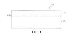
- FIG. 1illustrates an embodiment of a semiconductor on insulator structure 100 .
- Semiconductor on insulator structure 100includes a substrate 105 , and a semiconductor layer 110 bonded to substrate 105 .
- Semiconductor on insulator structure 100is configured with semiconductor layer 110 of a different material than substrate 105 , where the coefficient of thermal expansion of substrate 105 is substantially equal to that of semiconductor layer 110 .
- semiconductor layer 110also has a thickness such that semiconductor layer 110 does not yield due to temperature-induced strain at device processing temperatures. Temperature-induced strain includes strain that is produced in a material combined with another material as a result of mismatches in the coefficients of thermal expansion of the two materials.
- substrate 105has a material composition that includes a semiconductor that is within the semiconductor layer 110 .
- substrate 105has a material composition that includes oxygen.
- substrate 105has a material composition that includes an element, where the concentration of the element is controlled such that the coefficient of thermal expansion of substrate 105 substantially matches the coefficient of thermal expansion of semiconductor layer 110 .
- substrate 105has a material composition that includes carbon, where the carbon concentration is such that the coefficient of thermal expansion of substrate 105 substantially matches the coefficient of thermal expansion of semiconductor layer 110 .
- substrate 105is a silicon oxycarbide substrate.
- semiconductor layer 110includes silicon.
- an insulator layer 112is disposed between semiconductor layer 110 and substrate 105 .
- Insulator layer 112can be an oxide of a semiconductor material contained in semiconductor layer 110 .
- semiconductor layer 110is a silicon layer.
- insulator layer 112is a silicon oxide, which can include a native silicon oxide.
- insulator layer 112is not limited to an oxide and can include other insulator materials. Insulator layer 112 provides further reduction of stray capacitances and/or be used in processing device circuitry in the semiconductor on insulator structure.
- semiconductor layer 110can include and is not limited to a semiconductor layer containing germanium, gallium arsenide, a silicon-germanium compound, and other semiconductor materials as are known to those skilled in the art.
- substrates with coefficients of thermal expansion matched to the semiconductor layer formed on the substrate to provide a semiconductor on insulator structure, such as a silicon layer on or above a silicon oxycarbide glass substrateprovides economic benefits. These substrates serve to reduce the energy consumption and costs of fabricating a microchip that are typically associated with producing high quality crystalline substrates in which the majority of the substrate is not used in any device function and serves only as a carrier substrate. The use of high quality, high cost crystalline substrates as such a carrier substrate is typically not an efficient use of resources.
- a silicon on insulator structurewhere the silicon is bonded to a substrate
- problems during device formation using varying temperature processes
- One of the problems associated with temperature processing in a bonded wafer technologyinvolves the difference in coefficients of thermal expansion between the bonded materials.
- the coefficients of thermal expansion for some commonly used materialsincludes silicon carbide with a coefficient of thermal expansion of 4.0 to 3.9 ⁇ 10 ⁇ 6 cm/(cm K), silicon oxide with a coefficient of thermal expansion of 0.5 ⁇ 10 ⁇ 6 cm/(cm K), and silicon with a coefficient of thermal expansion of 2.6 ⁇ 10 ⁇ 6 cm/(cm K).
- FIG. 2provides an example of the limits on strain versus silicon layer thickness, where the dashed line 200 delineates the onset for yield, plastic deformation and defects in bulk silicon samples. If the strain is too large the materials will plastically deform by the introduction of dislocations, fracture and yield, or undergo excessive wafer bowing and/or warping.
- An approach to reduce stressincludes bonding silicon onto compliant substrates using low viscosity borophosphorosilicate glass films, which flows to reduce the stress.
- a semiconductor on insulator structureincludes a semiconductor layer formed on or above an insulating substrate of a different material than the semiconductor layer, where the coefficients of thermal expansion of the semiconductor layer and the substrate are substantially equal.
- a semiconductor on insulatorincludes a thin semiconductor layer bonded to a substrate, where the thin semiconductor layer also has a thickness such that the semiconductor layer does not yield due to temperature-induced strain at device processing temperatures.
- the thin semiconductor layeris an ultra-thin silicon layer having a thickness ranging from about 0.1 microns to about 10 microns. An ultra-thin silicon layer of about 0.1 microns can tolerate the strain introduced by thermal cycling and the differences in thermal expansion coefficients. A 1000° C. temperature difference will only produce a strain of about 0.21%, which, as shown in FIG. 2, is not sufficient to cause the thin silicon layer to yield.
- Insulating substrates in various embodimentsmay include glass substrates.
- Glass substratessuch as silicon oxycarbide glass substrates, can be provided in the form of wafers at costs significantly less than the costs associated with providing high quality, crystalline semiconductor wafers. Thus, application of these materials in semiconductor device processing can reduce the overall cost to manufacture the device.
- devices using the semiconductor on insulator structure of the present inventioninclude circuitry in a semiconductor layer.
- the circuitryis configured in a silicon layer bonded to a substrate.
- the silicon layeris monocrystalline allowing circuitry in the silicon layer, such as transistors, to have the performance level associated with devices having structures using single crystalline form. Having devices using single crystalline structures avoids the problems associated with grain boundaries of polycrystalline devices such as thin film polycrystalline transistors.
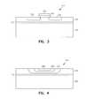
- FIG. 3depicts an embodiment of an electronic device 300 using a semiconductor on insulator structure.
- Electronic device 300includes an insulating substrate 305 , a thin semiconductor layer 310 bonded to insulating substrate 305 , and circuitry in thin semiconductor layer 310 , where semiconductor layer 310 has a material composition different than insulating substrate 305 and has a coefficient of thermal expansion substantially equal to that of insulating substrate 305 .
- semiconductor layer 310also has a thickness such that the semiconductor layer does not yield due to temperature-induced strain at device processing temperatures.
- FIG. 3also depicts a transistor having a source 320 , a drain 330 , a gate dielectric 340 disposed on substrate 310 covering the substrate region between source 320 and drain 330 , and a gate 350 disposed on gate dielectric 340 , where the transistor is an example of the circuitry for an electronic device 300 using a semiconductor on insulator structure.
- An embodiment of an electronic device using a semiconductor on insulator as described hereinis not limited to a transistor, but includes electronic devices using such a semiconductor on insulator structure.
- the circuitry of electronic device 300includes a memory circuit.
- electronic device 300can include an insulating layer 312 between thin semiconductor layer 310 and insulating substrate 305 .
- Insulator layer 312can be a oxide of a semiconductor material contained in semiconductor layer 310 .
- semiconductor layer 310is a silicon layer.
- semiconductor layer 310is a silicon layer having an insulating layer 312 , where insulator layer 312 is a silicon oxide, which can include a native silicon oxide.
- insulator layer 312is not limited to an oxide and can include other insulator materials.
- semiconductor layer 310can include and is not limited to a semiconductor layer containing silicon, germanium, gallium arsenide, a silicon-germanium compound, and other semiconductor materials as are known to those skilled in the art.
- CMOS device 300includes fully depleted devices using CMOS device technology, and various embodiments include partially depleted devices.
- Devices using a partially depleted CMOS processcan be configured with or without floating bodies. The structure, formation, and operation of CMOS devices are understood by those skilled in the art.
- FIG. 4depicts an embodiment of an electronic device 400 using a semiconductor on insulator structure.
- Electronic device 400includes an insulating substrate 405 , a thin semiconductor layer 410 bonded to insulating substrate 405 , and circuitry in thin semiconductor layer 410 , where semiconductor layer 410 has a material composition different than insulating substrate 405 and has a coefficient of thermal expansion substantially equal to that of insulating substrate 405 .
- semiconductor layer 410also has a thickness such that the semiconductor layer 410 does not yield due to temperature-induced strain at device processing temperatures.
- bipolar transistor 4also depicts a bipolar transistor having a collector 420 , a base 430 , and an emitter 440 disposed in semiconductor layer 410 , where the bipolar transistor is another example of the circuitry for an electronic device 400 using a semiconductor on insulator structure.
- An embodiment of an electronic device using a semiconductor on insulator as described hereinis not limited to a bipolar transistor, but includes electronic devices using such a semiconductor on insulator structure.
- electronic device 400includes circuitry for an integrated circuit.
- electronic device 400can include an insulating layer 412 between thin semiconductor layer 410 and insulating substrate 405 .
- Insulator layer 412can be a oxide of a semiconductor material contained in semiconductor layer 410 .
- semiconductor layer 410is a silicon layer.
- semiconductor layer 410is a silicon layer having an insulating layer 412 , where insulator layer 412 is a silicon oxide, which can include a native silicon oxide.
- insulator layer 412is not limited to an oxide and can include other insulator materials.
- semiconductor layer 410can include and is not limited to a semiconductor layer containing silicon, germanium, gallium arsenide, a silicon-germanium compound, and other semiconductor materials as are known to those skilled in the art.
- Embodiments for electronic devices using semiconductor on insulator structures as described hereinhave an isolated device area realized on an insulating substrate. Stray capacitances are minimized because the device drain, source, and/or collectors are on an insulating substrate. Interconnection wire is configured over an isolation oxide and the insulating substrate to minimize wiring capacitance. Reducing these parasitic capacitances reduces power consumption during circuit operation and increases the speed of operation.
- FIG. 5is a simplified block diagram of a memory device 500 using an embodiment of a semiconductor on insulator structure.
- Memory device 500includes an array of memory cells 502 , address decoder 504 , row access circuitry 506 , column access circuitry 508 , control circuitry 510 , and input/output (I/O) circuit 512 .
- the memoryis operably coupled to an external microprocessor 514 , or memory controller for memory accessing.
- Memory device 500receives control signals from processor 514 , such as WE*, RAS* and CAS* signals, which can be supplied on a system bus.
- Memory device 500stores data that is accessed via I/O lines.
- At least one of the integrated circuit structuresis formed in a silicon layer that is part of a semiconductor on insulator structure, such as a silicon on silicon oxycarbide glass structure, according to an embodiment.
- a memory deviceis intended to provide a general understanding of the memory and is not a complete description of all the elements and features of a specific type of memory, such as DRAM (Dynamic Random Access Memory). Further, embodiments are equally applicable to any size and type of memory circuit and are not intended to be limited to the DRAM described above. Other alternative types of devices include SRAM (Static Random Access Memory) or Flash memories.
- the DRAMcould be a synchronous DRAM commonly referred to as SGRAM (Synchronous Graphics Random Access Memory), SDRAM (Synchronous Dynamic Random Access Memory), SDRAM II, and DDR SDRAM (Double Data Rate SDRAM), as well as Synchlink or Rambus DRAMs and other emerging DRAM technologies.
- SGRAMSynchronous Graphics Random Access Memory
- SDRAMSynchronous Dynamic Random Access Memory
- SDRAM IISynchroble Data Rate SDRAM
- DDR SDRAMDouble Data Rate SDRAM
- FIG. 6illustrates a block diagram for an electronic system 600 having devices using an embodiment for a semiconductor on insulator structure.
- Electronic system 600includes a controller 605 , a bus 615 , and an electronic device 625 , where bus 615 provides electrical conductivity between controller 605 and electronic device 625 .
- controller 605 and/or electronic device 625includes an embodiment for a semiconductor on insulator structure as previously discussed having a substrate and a semiconductor layer bonded to the substrate.
- the substrate of a different material than the semiconductor layerhas a coefficient of thermal expansion substantially equal to that of the semiconductor layer.
- the semiconductor layeralso has a thickness such that the semiconductor layer does not yield due to temperature-induced strain at device processing temperatures.
- electronic system 600includes a plurality of electronic devices using an embodiment for a semiconductor on insulator structure.
- Electronic system 600may include, but is not limited to, information handling systems, wireless systems, telecommunication systems, fiber optic systems, electro-optic systems, and computers.
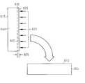
- FIG. 7illustrates an embodiment for matching a substrate with a semiconductor layer, according to the present invention.
- FIG. 7illustrates matching a silicon oxycarbide substrate with a silicon layer by selecting the carbon content of the silicon oxycarbide substrate.
- a multiple element materialis selected for the substrate on which to form the given semiconductor layer to provide a semiconductor on insulator structure.
- An element of the multiple element materialcan be varied in concentration to engineer a substrate with a selected, or predetermined, coefficient of thermal expansion.
- the controlled elementacts as a matching element such that the selected, or predetermined, coefficient of thermal expansion is chosen to match the coefficient of thermal expansion of the given semiconductor layer to be formed on the substrate.
- a matching element in a multiple element materialcan be varied by replacing another element in a multiple element material ranging from little or no concentration of the matching element shown at 710 in FIG. 7 to total replacement of an element at 720 along line 730 , as illustrated in FIG. 7.
- the percent concentration of the matching elementis chosen such that the coefficient of thermal expansion matches that of the given semiconductor layer at 740 .
- oxygenis the element of a multiple element material that is replaced at an amount depending on the material of the semiconductor layer to be matched.
- carbonis the matching element.
- silicon oxycarbideis the multiple element material used for a substrate with carbon acting as the replacing element. With no carbon in the multiple element material, it is a silicon oxide material at 710 in FIG. 7, while with a 100% replacement of the oxygen with carbon, the multiple element material is silicon carbide at 720 in FIG. 7.
- the coefficient of thermal expansion for silicon oxideis significantly lower than that of silicon, while the coefficient of thermal expansion for silicon carbide is significantly higher than that of silicon.
- silicon oxycarbide glasseshave a coefficient of thermal expansion larger than that of vitreous silica or silicon oxide.
- the coefficient of thermal expansion of the silicon oxycarbide substratecan substantially match that of the silicon semiconductor layer.
- the matching of the coefficient of thermal expansion for silicon oxycarbide with that of siliconcan be realized with a carbon concentration of approximately 60% to 70%, replacing oxygen.
- Other materials for the semiconductor layer and other multiple element materials for the substratecan be used in various embodiments in accordance with the teachings of the present invention.
- silicon oxycarbide glassescan be fabricated that are stable amorphous glass plates up to temperatures of 1200° C.
- Thin silicon oxycarbide glass sheetsare synthesized by the pyrolysis of gel sheets obtained from a methyl-modified silica sol containing colloidal silica under an inert atmosphere at temperatures ranging from 900 to 1200° C.
- the silicon oxycarbide glass substrate sheetsare polished and cut into wafer size patterns to act as substrate wafers. After patterning they can be further chemically and mechanically polished.
- FIG. 8illustrates the relationship of elements in an embodiment for a method to form a semiconductor on insulator structure.
- An embodiment for a method to form a semiconductor on insulator structureincludes providing a substrate and forming a semiconductor layer on or above the substrate, where the substrate is an insulating material that is a different material than the semiconductor layer and has a coefficient of thermal expansion that is approximately equal to the coefficient of thermal expansion for the semiconductor layer.
- the substrateis provided with a material composition that includes a semiconductor element that is in the semiconductor layer.
- the substrateis provided with a material composition that includes oxygen.
- the substrateis provided with a material composition that includes carbon.
- the substrateis provided with a material composition that includes a silicon oxycarbide substrate having its carbon concentration adjusted to substantially match the coefficient of thermal expansion of the silicon oxycarbide substrate with than of the semiconductor layer.
- the semiconductor layeris also formed as a bonded semiconductor layer having a thickness such that the semiconductor layer does not yield due to temperature-induced strain at device processing temperatures.
- An embodiment for a method to form a semiconductor on insulator structureincludes providing an insulating substrate, providing a semiconductor wafer, and performing a bonding cut process on the semiconductor wafer and the substrate to provide a thin semiconductor layer bonded to the substrate.
- the coefficients of thermal expansion of the substrate and the semiconductor layerare substantially equal.
- the semiconductor layer bonded to the substratealso has a thickness such that the semiconductor layer does not yield due to temperature-induced strain at device processing temperatures.
- a bonding cut processrefers to a process in which two substrates, or wafers, are bonded together and a section of at least one of the two wafers is cut or broken off after attaching the two wafers together.
- the waferis conditioned prior to the actual cut by implanting atoms to a predetermined distance into the wafer to be cut.
- the attached wafersare heated to cut the conditioned wafers and to bond further the remaining portions of the two wafers at the attachment plane.
- the section removed from a conditioned waferis the section of the conditioned wafer from the end of the conditioned wafer, which is away from the attachment to the other wafer, to the plane along the conditioned wafer that is at the distance to which the implantation was made.
- the removed sectionincludes a significant portion of the original wafer, with the smaller portion that was subjected to implantation remaining bonded to the other wafer.
- insulating substrate 805 provided for fabricating a semiconductor on insulator structureincludes a substrate that has been processed to have a coefficient of thermal expansion substantially equal to that of the semiconductor selected to form the semiconductor on insulator structure.
- the substrate materialcan include silicon oxycarbide glass.
- the substrateis generated from thin silicon oxycarbide glass sheets. These silicon oxycarbide glass sheets are polished and cut into wafer size patterns to act as substrates for integrated circuits. These wafer size silicon oxycarbide glass sheets for forming substrates are relatively inexpensive as compared with silicon substrates. After patterning the substrates, these substrates can be further chemically and mechanically polished.
- Semiconductor wafer 815is conditioned as part of the bonding cut process prior to bonding to substrate 805 .
- Semiconductor wafer 815can include wafers having semiconductor material that includes, but is not limited to, silicon, germanium, silicon-germanium, gallium arsenide, indium phosphide, and other semiconductor materials.
- semiconductor materialincludes, but is not limited to, silicon, germanium, silicon-germanium, gallium arsenide, indium phosphide, and other semiconductor materials.
- Insulating substrate 805can be considered as a matching substrate to semiconductor layer 815 .
- Silicon wafer 815such as a single crystal wafer, is conditioned by subjecting a surface 820 to implantation of ions 825 to form an intermediate silicon layer 830 having a thickness 835 .
- the ionsare implanted along a plane 840 , represented in FIG. 8 as a line, which is approximately parallel to surface 820 .
- hydrogen ionsare used as implantation ions 825 .
- the hydrogen ionscan take the form of H + , H 2 + , D + , or D 2 + ions.
- the implanted ionsact to form cavities along the cleavage plane 840 .
- the cavitiesare joined through thermal processing. Once these cavities join, the wafer becomes cut or broken off along plane 840 .
- silicon wafer 815is also conditioned by forming an oxide on surface 820 .
- the oxidecan include a native oxide.
- the ion implantationcan be performed before or after the oxide formation.
- silicon wafer 815 and substrate 805can be cleaned using conventional cleaning procedures.
- silicon wafer 815is also conditioned by forming an oxide on surface 820 before applying a cleaning procedure.
- surface 820 of silicon wafer 815with or without an oxide layer formed thereon, is attached to a surface 810 of substrate 805 .
- This attachment of silicon wafer 815 to substrate 805is typically by Van der Walls forces.
- silicon wafer 815is further bonded to substrate 805 causing a section 850 of silicon wafer 815 to cut or break off along cleavage plane 840 .
- intermediate silicon layer 830is bonded to substrate 805 .
- Intermediate silicon layer 830is defined by the depth of ion implantation to line 840 and has a thin thickness 835 .
- thickness 835is generated to a thickness such that intermediate silicon layer 830 does not yield due to temperature-induced strain at device processing temperatures allowing intermediate silicon layer 830 to be used as the thin semiconductor layer 110 as depicted in FIG. 1.
- intermediate silicon layer 830has a thickness ranging from about 0.1 microns to about 10 microns.
- section 850is relatively thick and has the form of a silicon wafer. Section 850 can be used with another insulating substrate to form another silicon on insulator structure, during which fabrication another remaining section from the bond cut process becomes available to be used with yet another substrate. This reduces the overall cost for the manufacturing process of a wide variety of electronic devices.
- plasma enhanced bondingis used to bond intermediate silicon layer 830 to substrate 805 and cut or break off section 850 .
- the bonding cut processincludes raising the temperature of silicon wafer 815 attached to substrate 805 to a temperature ranging from about 400° C. to about 600° C. to cut or break off section 850 . Then, the resulting bond between intermediate silicon layer 830 and substrate 805 can be strengthened by raising the temperature to a range from about 800° C. to about 1000° C. or annealing by laser assisted annealing.
- bonding of the silicon wafer 815can be accomplished with anodic bonding, anodic bonding for a CMOS process introduces high alkali concentration, which is not appropriate for the CMOS process.
- intermediate silicon layer 830that is bonded to substrate 805 , with or without an insulating layer between silicon layer 830 and substrate 805 , thins intermediate silicon layer 830 .
- This subsequent polishing processesprovides a thin silicon layer for the silicon on insulator structure.
- intermediate silicon layer 830is polished to provide an ultra-thin silicon layer having a thickness of about 0.1 microns.
- intermediate silicon layer 830is polished to provide a silicon layer having a thickness ranging from about 0.1 microns to about 10 microns.
- a silicon on insulator structureis ready for device processing.
- an silicon oxycarbide substratecan be used as the matching substrate for the silicon layer.
- removed section 850can be used to fabricate other silicon on insulator wafers.
- embodimentsinclude other semiconductor materials in place of the silicon to provide a semiconductor layer on a substrate of a different material composition, where the coefficient of thermal expansion of the substrate matches that of the semiconductor layer.
- the semiconductor layeris also formed having a thickness such that the semiconductor layer does not yield due to temperature-induced strain at device processing temperatures. Thermal processing for the bond cut is performed by temperatures appropriate for the semiconductor wafer and matching substrate used.
- CMOS devicescan be fabricated by masking device areas with oxide and nitride and oxidizing the silicon in between device mesas, followed by conventional device fabrication techniques.
- partially depleted CMOS devicescan be formed with or without floating bodies.
- a layer of silicon thicker than for a fully depleted CMOS processis used and the thicker silicon layer is patterned by a trench isolation process similar to a SIMOX process. After patterning the silicon layer by the trench isolation, conventional techniques are used to process the device.
- heavily doped collector patternsare formed in the silicon wafer prior to performing the bonding cut process to bond the silicon to the matching substrate.
- the silicon layer bonded to the matching surfaceis relatively thick.
- patterned base and emitter implantationsare formed in the surface of the silicon layer. Further device processing is performed using conventional techniques.
- an isolated silicon device areais realized on an insulating substrate. Stray capacitances are minimized because the device drain, source, and/or collectors are on an insulating substrate. Interconnection wire is configured over an isolation oxide and the insulating substrate to minimize wiring capacitance. Reducing these parasitic capacitances reduces power consumption during circuit operation and increases the speed of operation.
- a method including the procedures and processes for forming a semiconductor on insulator structure and for forming devices and systems with elements using a semiconductor on insulator structureare controlled by a computer.
- the instructions for the methodare stored in a computer readable format on a computer readable media. Examples of such computer readable media include but are not limited to laser readable disks, magnetic disks and tape, and computer memory.
- Embodiments of the present inventioninclude the use of substrates that serve to reduce the energy consumption and costs of fabricating a microchip that are typically associated with producing high quality crystalline substrates.
- Forming a semiconductor layer on or above a substrate, such as a silicon layer on or above a silicon oxycarbide glass substrate, in which the coefficient of thermal expansion of the substrate is matched to that of the semiconductor layer,has several attributes. By bonding a semiconductor layer to such a matched substrate, problems associated with differences in the coefficient of thermal expansion can be avoided.
- the cost associated with providing such matched substratesis significantly less than the cost for providing high quality semiconductor wafers such as silicon wafers.
- Performing a bond cut process as described hereinallows a thin semiconductor layer to be taken from a high quality semiconductor wafer, such as a silicon wafer, to form a semiconductor on insulator wafer and at the same time provide for use of the same high quality semiconductor wafer to form multiple semiconductor on insulator structures.
- semiconductor on insulator wafers formed according to the various embodimentsprovide an isolated device area on an insulating substrate where stray device capacitances and wiring capacitances are minimized. Reducing these parasitic capacitances reduces power consumption during circuit operation and increases the speed of operation.
Landscapes
- Engineering & Computer Science (AREA)
- Physics & Mathematics (AREA)
- Condensed Matter Physics & Semiconductors (AREA)
- General Physics & Mathematics (AREA)
- Manufacturing & Machinery (AREA)
- Computer Hardware Design (AREA)
- Microelectronics & Electronic Packaging (AREA)
- Power Engineering (AREA)
- Thin Film Transistor (AREA)
- Element Separation (AREA)
- Metal-Oxide And Bipolar Metal-Oxide Semiconductor Integrated Circuits (AREA)
Abstract
Description
- This application is related to the following commonly assigned U.S. patent application, U.S. application Ser. No. ______, entitled: “Ultra-Thin Semiconductors Bonded on Substrates,” filed ______, which is herein incorporated by reference in its entirety.[0001]
- This application relates generally to electronic devices and device fabrication and, in particular, semiconductor on insulator devices and their fabrication.[0002]
- Almost half the energy expended by a silicon microchip during its manufacture and lifetime is spent in producing the silicon wafer material, and another quarter is spent during the operating lifetime of the microchip. A technique that reduces the energy associated with fabrication of the silicon material and power consumption during operation will reduce the overall cost of the silicon microchip integrated circuit.[0003]
- Power consumption during operation can be reduced using silicon on insulator (SOI) technology. The use of SOI technology not only results in a lower power consumption but also increased speed of operation of integrated circuits due to a reduction in stray capacitance. For SOI structures, thin layers of silicon on insulator can be fabricated using several well known techniques such as separation by implantation of oxygen (SIMOX), separation by plasma implantation of oxygen (SPIMOX), silicon on sapphire (SOS), bonded wafer processes on silicon, and silicon bonded on sapphire.[0004]
- Bonded wafer processes on silicon involve technologies to bond monocrystalline silicon materials onto semiconductor wafers and oxidation processes to form the semiconductor on insulator. In these technologies, a portion of one or both of the bonded wafers is removed, typically, by polishing methods.[0005]
- Another process to remove large portions of a bonded wafer uses a “Smart cut” technology. “Smart cut” technology generally refers to a process in which a material is implanted into a silicon substrate to a particular depth and ultimately utilized to crack the substrate.[0006]
- There continues to be a need to provide fabrication processes and structures to reduce the overall cost for a silicon microchip integrated circuit.[0007]
- The abovementioned problems are addressed by the present invention and will be understood by reading and studying the following specification. An embodiment of a method for forming a semiconductor on insulator structure includes providing a substrate and forming a semiconductor layer on the substrate, where the substrate is a material different than the semiconductor. The substrate has a coefficient of thermal expansion that is substantially equal to the coefficient of thermal expansion of the semiconductor layer. In an embodiment, the substrate is a compound of several elements and is formed by controlling the concentration of an element of the compound to provide the resulting substrate with a coefficient of thermal expansion substantially matched to that of a semiconductor to be formed on the substrate. In an embodiment, a silicon layer is bonded to a silicon oxycarbide substrate having a coefficient of thermal expansion substantially equal to that of the silicon layer. In embodiment, a thin semiconductor layer is formed on a substrate by a bonding cut process on a semiconductor wafer and the substrate, where the semiconductor layer and the substrate are different materials having substantially equal coefficients of thermal expansion. In an embodiment, a silicon layer bonded to a substrate provides a silicon on insulator structure in which circuitry for electronic devices is configured.[0008]
- These and other aspects, embodiments, advantages, and features will become apparent from the following description and the referenced drawings.[0009]
- FIG. 1 illustrates an embodiment of a semiconductor on insulator, according to the present invention.[0010]
- FIG. 2 illustrates a relationship between silicon layer thickness and strain.[0011]
- FIG. 3 depicts an embodiment of an electronic device using a semiconductor on insulator structure, according to the present invention.[0012]
- FIG. 4 depicts an embodiment of another electronic device using a semiconductor on insulator structure, according to the present invention.[0013]
- FIG. 5 is a simplified block diagram of a memory device using an embodiment of a semiconductor on insulator structure, according to the present invention.[0014]
- FIG. 6 illustrates a block diagram for an electronic system having devices that use an embodiment of a semiconductor on insulator structure, according to the present invention.[0015]
- FIG. 7 illustrates an embodiment for matching a substrate with a semiconductor layer, according to the present invention.[0016]
- FIG. 8 illustrates the relationship of elements in an embodiment for a method to form a semiconductor on insulator structure, according to the present invention.[0017]
- The following detailed description refers to the accompanying drawings that show, by way of illustration, specific aspects and embodiments in which the present invention may be practiced. These embodiments are described in sufficient detail to enable those skilled in the art to practice the present invention. Other embodiments may be utilized and structural, logical, and electrical changes may be made without departing from the scope of the present invention. The various embodiments disclosed herein are not necessarily mutually exclusive, as some disclosed embodiments can be combined with one or more other disclosed embodiments to form new embodiments.[0018]
- The terms wafer and substrate used in the following description include any structure having an exposed surface with which to form an integrated circuit (IC) structure. The term substrate is understood to include semiconductor wafers. Both wafer and substrate can include doped and undoped semiconductors, epitaxial semiconductor layers supported by a base semiconductor or insulator, as well as other semiconductor structures well known to one skilled in the art. The following detailed description is, therefore, not to be taken in a limiting sense, and the scope of the present invention is defined only by the appended claims, along with the full scope of equivalents to which such claims are entitled.[0019]
- FIG. 1 illustrates an embodiment of a semiconductor on[0020]
insulator structure 100. Semiconductor oninsulator structure 100 includes asubstrate 105, and asemiconductor layer 110 bonded tosubstrate 105. Semiconductor oninsulator structure 100 is configured withsemiconductor layer 110 of a different material thansubstrate 105, where the coefficient of thermal expansion ofsubstrate 105 is substantially equal to that ofsemiconductor layer 110. In an embodiment,semiconductor layer 110 also has a thickness such thatsemiconductor layer 110 does not yield due to temperature-induced strain at device processing temperatures. Temperature-induced strain includes strain that is produced in a material combined with another material as a result of mismatches in the coefficients of thermal expansion of the two materials. - In an embodiment,[0021]
substrate 105 has a material composition that includes a semiconductor that is within thesemiconductor layer 110. In an embodiment,substrate 105 has a material composition that includes oxygen. In an embodiment,substrate 105 has a material composition that includes an element, where the concentration of the element is controlled such that the coefficient of thermal expansion ofsubstrate 105 substantially matches the coefficient of thermal expansion ofsemiconductor layer 110. In an embodiment,substrate 105 has a material composition that includes carbon, where the carbon concentration is such that the coefficient of thermal expansion ofsubstrate 105 substantially matches the coefficient of thermal expansion ofsemiconductor layer 110. In an embodiment,substrate 105 is a silicon oxycarbide substrate. In an embodiment,semiconductor layer 110 includes silicon. - In an embodiment, an[0022]
insulator layer 112 is disposed betweensemiconductor layer 110 andsubstrate 105.Insulator layer 112 can be an oxide of a semiconductor material contained insemiconductor layer 110. In an embodiment,semiconductor layer 110 is a silicon layer. In an embodiment wheresemiconductor layer 110 is a silicon layer havinginsulator layer 112,insulator layer 112 is a silicon oxide, which can include a native silicon oxide. However,insulator layer 112 is not limited to an oxide and can include other insulator materials.Insulator layer 112 provides further reduction of stray capacitances and/or be used in processing device circuitry in the semiconductor on insulator structure. Additionally,semiconductor layer 110 can include and is not limited to a semiconductor layer containing germanium, gallium arsenide, a silicon-germanium compound, and other semiconductor materials as are known to those skilled in the art. - The use of substrates with coefficients of thermal expansion matched to the semiconductor layer formed on the substrate to provide a semiconductor on insulator structure, such as a silicon layer on or above a silicon oxycarbide glass substrate, provides economic benefits. These substrates serve to reduce the energy consumption and costs of fabricating a microchip that are typically associated with producing high quality crystalline substrates in which the majority of the substrate is not used in any device function and serves only as a carrier substrate. The use of high quality, high cost crystalline substrates as such a carrier substrate is typically not an efficient use of resources.[0023]
- In addition to efficient use of resources, there are fabrication issues associated with processing devices in a wafer at elevated temperatures. For instance, a silicon on insulator structure, where the silicon is bonded to a substrate, is subject to problems during device formation using varying temperature processes. One of the problems associated with temperature processing in a bonded wafer technology involves the difference in coefficients of thermal expansion between the bonded materials. For example, the coefficients of thermal expansion for some commonly used materials includes silicon carbide with a coefficient of thermal expansion of 4.0 to 3.9×[0024]10−6cm/(cm K), silicon oxide with a coefficient of thermal expansion of 0.5×10⁻⁶cm/(cm K), and silicon with a coefficient of thermal expansion of 2.6×10⁻⁶cm/(cm K). Associated with these differences in the coefficients of thermal expansion is the creation of excessive stress when bonding thick layers when there is a mismatch in the coefficients of thermal expansion. The development of excessive stress can result in exceeding the strain limit of the materials. FIG. 2 provides an example of the limits on strain versus silicon layer thickness, where the dashed
line 200 delineates the onset for yield, plastic deformation and defects in bulk silicon samples. If the strain is too large the materials will plastically deform by the introduction of dislocations, fracture and yield, or undergo excessive wafer bowing and/or warping. An approach to reduce stress includes bonding silicon onto compliant substrates using low viscosity borophosphorosilicate glass films, which flows to reduce the stress. - In an embodiment according to the present invention, a semiconductor on insulator structure includes a semiconductor layer formed on or above an insulating substrate of a different material than the semiconductor layer, where the coefficients of thermal expansion of the semiconductor layer and the substrate are substantially equal. In an embodiment, a semiconductor on insulator includes a thin semiconductor layer bonded to a substrate, where the thin semiconductor layer also has a thickness such that the semiconductor layer does not yield due to temperature-induced strain at device processing temperatures. In an embodiment, the thin semiconductor layer is an ultra-thin silicon layer having a thickness ranging from about 0.1 microns to about 10 microns. An ultra-thin silicon layer of about 0.1 microns can tolerate the strain introduced by thermal cycling and the differences in thermal expansion coefficients. A 1000° C. temperature difference will only produce a strain of about 0.21%, which, as shown in FIG. 2, is not sufficient to cause the thin silicon layer to yield.[0025]
- Insulating substrates in various embodiments may include glass substrates. Glass substrates, such as silicon oxycarbide glass substrates, can be provided in the form of wafers at costs significantly less than the costs associated with providing high quality, crystalline semiconductor wafers. Thus, application of these materials in semiconductor device processing can reduce the overall cost to manufacture the device.[0026]
- In embodiments, devices using the semiconductor on insulator structure of the present invention include circuitry in a semiconductor layer. In an embodiment, the circuitry is configured in a silicon layer bonded to a substrate. The silicon layer is monocrystalline allowing circuitry in the silicon layer, such as transistors, to have the performance level associated with devices having structures using single crystalline form. Having devices using single crystalline structures avoids the problems associated with grain boundaries of polycrystalline devices such as thin film polycrystalline transistors.[0027]
- FIG. 3 depicts an embodiment of an[0028]
electronic device 300 using a semiconductor on insulator structure.Electronic device 300 includes an insulatingsubstrate 305, athin semiconductor layer 310 bonded to insulatingsubstrate 305, and circuitry inthin semiconductor layer 310, wheresemiconductor layer 310 has a material composition different than insulatingsubstrate 305 and has a coefficient of thermal expansion substantially equal to that of insulatingsubstrate 305. In an embodiment,semiconductor layer 310 also has a thickness such that the semiconductor layer does not yield due to temperature-induced strain at device processing temperatures. FIG. 3 also depicts a transistor having asource 320, adrain 330, agate dielectric 340 disposed onsubstrate 310 covering the substrate region betweensource 320 and drain330, and agate 350 disposed ongate dielectric 340, where the transistor is an example of the circuitry for anelectronic device 300 using a semiconductor on insulator structure. An embodiment of an electronic device using a semiconductor on insulator as described herein is not limited to a transistor, but includes electronic devices using such a semiconductor on insulator structure. In an embodiment, the circuitry ofelectronic device 300 includes a memory circuit. - In an embodiment for electronic device, in addition to insulating[0029]
substrate 305,electronic device 300 can include an insulatinglayer 312 betweenthin semiconductor layer 310 and insulatingsubstrate 305.Insulator layer 312 can be a oxide of a semiconductor material contained insemiconductor layer 310. In an embodiment,semiconductor layer 310 is a silicon layer. In an embodiment,semiconductor layer 310 is a silicon layer having an insulatinglayer 312, whereinsulator layer 312 is a silicon oxide, which can include a native silicon oxide. However,insulator layer 312 is not limited to an oxide and can include other insulator materials. Additionally,semiconductor layer 310 can include and is not limited to a semiconductor layer containing silicon, germanium, gallium arsenide, a silicon-germanium compound, and other semiconductor materials as are known to those skilled in the art. - Various embodiments of[0030]
electronic device 300 include fully depleted devices using CMOS device technology, and various embodiments include partially depleted devices. Devices using a partially depleted CMOS process can be configured with or without floating bodies. The structure, formation, and operation of CMOS devices are understood by those skilled in the art. - FIG. 4 depicts an embodiment of an[0031]
electronic device 400 using a semiconductor on insulator structure.Electronic device 400 includes an insulating substrate405, athin semiconductor layer 410 bonded to insulating substrate405, and circuitry inthin semiconductor layer 410, wheresemiconductor layer 410 has a material composition different than insulating substrate405 and has a coefficient of thermal expansion substantially equal to that of insulating substrate405. In an embodiment,semiconductor layer 410 also has a thickness such that thesemiconductor layer 410 does not yield due to temperature-induced strain at device processing temperatures. FIG. 4 also depicts a bipolar transistor having acollector 420, abase 430, and anemitter 440 disposed insemiconductor layer 410, where the bipolar transistor is another example of the circuitry for anelectronic device 400 using a semiconductor on insulator structure. An embodiment of an electronic device using a semiconductor on insulator as described herein is not limited to a bipolar transistor, but includes electronic devices using such a semiconductor on insulator structure. In an embodiment,electronic device 400 includes circuitry for an integrated circuit. - In an embodiment for electronic device, in addition to insulating substrate[0032]405,
electronic device 400 can include an insulatinglayer 412 betweenthin semiconductor layer 410 and insulating substrate405.Insulator layer 412 can be a oxide of a semiconductor material contained insemiconductor layer 410. In an embodiment,semiconductor layer 410 is a silicon layer. In an embodiment,semiconductor layer 410 is a silicon layer having an insulatinglayer 412, whereinsulator layer 412 is a silicon oxide, which can include a native silicon oxide. However,insulator layer 412 is not limited to an oxide and can include other insulator materials. Additionally,semiconductor layer 410 can include and is not limited to a semiconductor layer containing silicon, germanium, gallium arsenide, a silicon-germanium compound, and other semiconductor materials as are known to those skilled in the art. - Embodiments for electronic devices using semiconductor on insulator structures as described herein have an isolated device area realized on an insulating substrate. Stray capacitances are minimized because the device drain, source, and/or collectors are on an insulating substrate. Interconnection wire is configured over an isolation oxide and the insulating substrate to minimize wiring capacitance. Reducing these parasitic capacitances reduces power consumption during circuit operation and increases the speed of operation.[0033]
- FIG. 5 is a simplified block diagram of a[0034]
memory device 500 using an embodiment of a semiconductor on insulator structure.Memory device 500 includes an array ofmemory cells 502,address decoder 504,row access circuitry 506,column access circuitry 508,control circuitry 510, and input/output (I/O)circuit 512. The memory is operably coupled to anexternal microprocessor 514, or memory controller for memory accessing.Memory device 500 receives control signals fromprocessor 514, such as WE*, RAS* and CAS* signals, which can be supplied on a system bus.Memory device 500 stores data that is accessed via I/O lines. It will be appreciated by those skilled in the art that additional circuitry and control signals can be provided, and that the memory device of FIG. 5 has been simplified to help focus on the present invention. At least one of the integrated circuit structures is formed in a silicon layer that is part of a semiconductor on insulator structure, such as a silicon on silicon oxycarbide glass structure, according to an embodiment. - It will be understood that the above description of a memory device is intended to provide a general understanding of the memory and is not a complete description of all the elements and features of a specific type of memory, such as DRAM (Dynamic Random Access Memory). Further, embodiments are equally applicable to any size and type of memory circuit and are not intended to be limited to the DRAM described above. Other alternative types of devices include SRAM (Static Random Access Memory) or Flash memories. Additionally, the DRAM could be a synchronous DRAM commonly referred to as SGRAM (Synchronous Graphics Random Access Memory), SDRAM (Synchronous Dynamic Random Access Memory), SDRAM II, and DDR SDRAM (Double Data Rate SDRAM), as well as Synchlink or Rambus DRAMs and other emerging DRAM technologies.[0035]
- FIG. 6 illustrates a block diagram for an[0036]
electronic system 600 having devices using an embodiment for a semiconductor on insulator structure.Electronic system 600 includes acontroller 605, a bus615, and anelectronic device 625, where bus615 provides electrical conductivity betweencontroller 605 andelectronic device 625. In various embodiments,controller 605 and/orelectronic device 625 includes an embodiment for a semiconductor on insulator structure as previously discussed having a substrate and a semiconductor layer bonded to the substrate. The substrate of a different material than the semiconductor layer has a coefficient of thermal expansion substantially equal to that of the semiconductor layer. In an embodiment, the semiconductor layer also has a thickness such that the semiconductor layer does not yield due to temperature-induced strain at device processing temperatures. In an embodiment,electronic system 600 includes a plurality of electronic devices using an embodiment for a semiconductor on insulator structure.Electronic system 600 may include, but is not limited to, information handling systems, wireless systems, telecommunication systems, fiber optic systems, electro-optic systems, and computers. - FIG. 7 illustrates an embodiment for matching a substrate with a semiconductor layer, according to the present invention. In particular, FIG. 7 illustrates matching a silicon oxycarbide substrate with a silicon layer by selecting the carbon content of the silicon oxycarbide substrate.[0037]
- According to an embodiment of the present invention, for a given semiconductor layer, a multiple element material is selected for the substrate on which to form the given semiconductor layer to provide a semiconductor on insulator structure. An element of the multiple element material can be varied in concentration to engineer a substrate with a selected, or predetermined, coefficient of thermal expansion. The controlled element acts as a matching element such that the selected, or predetermined, coefficient of thermal expansion is chosen to match the coefficient of thermal expansion of the given semiconductor layer to be formed on the substrate.[0038]
- A matching element in a multiple element material can be varied by replacing another element in a multiple element material ranging from little or no concentration of the matching element shown at[0039]710 in FIG. 7 to total replacement of an element at720 along
line 730, as illustrated in FIG. 7. The percent concentration of the matching element is chosen such that the coefficient of thermal expansion matches that of the given semiconductor layer at740. In an embodiment, oxygen is the element of a multiple element material that is replaced at an amount depending on the material of the semiconductor layer to be matched. In an embodiment, carbon is the matching element. - In an embodiment, silicon oxycarbide is the multiple element material used for a substrate with carbon acting as the replacing element. With no carbon in the multiple element material, it is a silicon oxide material at[0040]710 in FIG. 7, while with a 100% replacement of the oxygen with carbon, the multiple element material is silicon carbide at720 in FIG. 7. For matching purposes, in an embodiment with silicon as the semiconductor layer, the coefficient of thermal expansion for silicon oxide is significantly lower than that of silicon, while the coefficient of thermal expansion for silicon carbide is significantly higher than that of silicon. However, silicon oxycarbide glasses have a coefficient of thermal expansion larger than that of vitreous silica or silicon oxide. By forming a silicon oxycarbide substrate in which carbon has replaced oxygen, the coefficient of thermal expansion of the silicon oxycarbide substrate can substantially match that of the silicon semiconductor layer. The matching of the coefficient of thermal expansion for silicon oxycarbide with that of silicon can be realized with a carbon concentration of approximately 60% to 70%, replacing oxygen. Other materials for the semiconductor layer and other multiple element materials for the substrate can be used in various embodiments in accordance with the teachings of the present invention.
- In an embodiment, silicon oxycarbide glasses can be fabricated that are stable amorphous glass plates up to temperatures of 1200° C. Thin silicon oxycarbide glass sheets are synthesized by the pyrolysis of gel sheets obtained from a methyl-modified silica sol containing colloidal silica under an inert atmosphere at temperatures ranging from 900 to 1200° C. The silicon oxycarbide glass substrate sheets are polished and cut into wafer size patterns to act as substrate wafers. After patterning they can be further chemically and mechanically polished.[0041]
- FIG. 8 illustrates the relationship of elements in an embodiment for a method to form a semiconductor on insulator structure. An embodiment for a method to form a semiconductor on insulator structure includes providing a substrate and forming a semiconductor layer on or above the substrate, where the substrate is an insulating material that is a different material than the semiconductor layer and has a coefficient of thermal expansion that is approximately equal to the coefficient of thermal expansion for the semiconductor layer. In an embodiment, the substrate is provided with a material composition that includes a semiconductor element that is in the semiconductor layer. In an embodiment, the substrate is provided with a material composition that includes oxygen. In an embodiment, the substrate is provided with a material composition that includes carbon. In an embodiment, the substrate is provided with a material composition that includes a silicon oxycarbide substrate having its carbon concentration adjusted to substantially match the coefficient of thermal expansion of the silicon oxycarbide substrate with than of the semiconductor layer. In an embodiment, the semiconductor layer is also formed as a bonded semiconductor layer having a thickness such that the semiconductor layer does not yield due to temperature-induced strain at device processing temperatures.[0042]
- An embodiment for a method to form a semiconductor on insulator structure includes providing an insulating substrate, providing a semiconductor wafer, and performing a bonding cut process on the semiconductor wafer and the substrate to provide a thin semiconductor layer bonded to the substrate. The coefficients of thermal expansion of the substrate and the semiconductor layer are substantially equal. In an embodiment, the semiconductor layer bonded to the substrate also has a thickness such that the semiconductor layer does not yield due to temperature-induced strain at device processing temperatures.[0043]
- Herein, a bonding cut process refers to a process in which two substrates, or wafers, are bonded together and a section of at least one of the two wafers is cut or broken off after attaching the two wafers together. For each wafer for which a section is cut or broken off, the wafer is conditioned prior to the actual cut by implanting atoms to a predetermined distance into the wafer to be cut. The attached wafers are heated to cut the conditioned wafers and to bond further the remaining portions of the two wafers at the attachment plane. The section removed from a conditioned wafer is the section of the conditioned wafer from the end of the conditioned wafer, which is away from the attachment to the other wafer, to the plane along the conditioned wafer that is at the distance to which the implantation was made. The removed section includes a significant portion of the original wafer, with the smaller portion that was subjected to implantation remaining bonded to the other wafer.[0044]
- In an embodiment, insulating[0045]
substrate 805 provided for fabricating a semiconductor on insulator structure includes a substrate that has been processed to have a coefficient of thermal expansion substantially equal to that of the semiconductor selected to form the semiconductor on insulator structure. The substrate material can include silicon oxycarbide glass. In an embodiment, the substrate is generated from thin silicon oxycarbide glass sheets. These silicon oxycarbide glass sheets are polished and cut into wafer size patterns to act as substrates for integrated circuits. These wafer size silicon oxycarbide glass sheets for forming substrates are relatively inexpensive as compared with silicon substrates. After patterning the substrates, these substrates can be further chemically and mechanically polished. - [0046]
Semiconductor wafer 815 is conditioned as part of the bonding cut process prior to bonding tosubstrate 805.Semiconductor wafer 815 can include wafers having semiconductor material that includes, but is not limited to, silicon, germanium, silicon-germanium, gallium arsenide, indium phosphide, and other semiconductor materials. For ease of discussion regarding embodiments according to the present invention, the remainder of this discussion focuses on an embodiment using a silicon wafer assemiconductor wafer 815 and insulatingsubstrate 805 in which the coefficients of thermal expansion forsilicon wafer 815 andsubstrate 805 are substantially equal. Insulatingsubstrate 805 can be considered as a matching substrate tosemiconductor layer 815. - [0047]
Silicon wafer 815, such as a single crystal wafer, is conditioned by subjecting asurface 820 to implantation ofions 825 to form anintermediate silicon layer 830 having athickness 835. The ions are implanted along aplane 840, represented in FIG. 8 as a line, which is approximately parallel tosurface 820. In an embodiment, hydrogen ions are used asimplantation ions 825. The hydrogen ions can take the form of H+, H2+, D+, or D2+ ions. The implanted ions act to form cavities along thecleavage plane 840. The cavities are joined through thermal processing. Once these cavities join, the wafer becomes cut or broken off alongplane 840. In an embodiment,silicon wafer 815 is also conditioned by forming an oxide onsurface 820. The oxide can include a native oxide. The ion implantation can be performed before or after the oxide formation. - After[0048]
conditioning silicon wafer 815,silicon wafer 815 andsubstrate 805 can be cleaned using conventional cleaning procedures. In an embodiment,silicon wafer 815 is also conditioned by forming an oxide onsurface 820 before applying a cleaning procedure. Then,surface 820 ofsilicon wafer 815, with or without an oxide layer formed thereon, is attached to asurface 810 ofsubstrate 805. This attachment ofsilicon wafer 815 tosubstrate 805 is typically by Van der Walls forces. Then,silicon wafer 815 is further bonded tosubstrate 805 causing asection 850 ofsilicon wafer 815 to cut or break off alongcleavage plane 840. - As a result of this bonding cut,[0049]
intermediate silicon layer 830 is bonded tosubstrate 805.Intermediate silicon layer 830 is defined by the depth of ion implantation toline 840 and has athin thickness 835. In an embodiment,thickness 835 is generated to a thickness such thatintermediate silicon layer 830 does not yield due to temperature-induced strain at device processing temperatures allowingintermediate silicon layer 830 to be used as thethin semiconductor layer 110 as depicted in FIG. 1. In an embodiment,intermediate silicon layer 830 has a thickness ranging from about 0.1 microns to about 10 microns. As a result of the thin nature ofintermediate silicon layer 830,section 850 is relatively thick and has the form of a silicon wafer.Section 850 can be used with another insulating substrate to form another silicon on insulator structure, during which fabrication another remaining section from the bond cut process becomes available to be used with yet another substrate. This reduces the overall cost for the manufacturing process of a wide variety of electronic devices. - In an embodiment, plasma enhanced bonding is used to bond[0050]
intermediate silicon layer 830 tosubstrate 805 and cut or break offsection 850. In an embodiment, the bonding cut process includes raising the temperature ofsilicon wafer 815 attached tosubstrate 805 to a temperature ranging from about 400° C. to about 600° C. to cut or break offsection 850. Then, the resulting bond betweenintermediate silicon layer 830 andsubstrate 805 can be strengthened by raising the temperature to a range from about 800° C. to about 1000° C. or annealing by laser assisted annealing. Though bonding of thesilicon wafer 815, with or without an oxide layer onsurface 820, can be accomplished with anodic bonding, anodic bonding for a CMOS process introduces high alkali concentration, which is not appropriate for the CMOS process. - In an embodiment, polishing[0051]
intermediate silicon layer 830 that is bonded tosubstrate 805, with or without an insulating layer betweensilicon layer 830 andsubstrate 805, thinsintermediate silicon layer 830. This subsequent polishing processes provides a thin silicon layer for the silicon on insulator structure. In an embodiment,intermediate silicon layer 830 is polished to provide an ultra-thin silicon layer having a thickness of about 0.1 microns. In an embodiment,intermediate silicon layer 830 is polished to provide a silicon layer having a thickness ranging from about 0.1 microns to about 10 microns. - Once the bond cut process is concluded providing a silicon layer bonded to a substrate, a silicon on insulator structure is ready for device processing. In the various embodiments discussed above, an silicon oxycarbide substrate can be used as the matching substrate for the silicon layer. Further, removed[0052]
section 850 can be used to fabricate other silicon on insulator wafers. As previously discussed, embodiments include other semiconductor materials in place of the silicon to provide a semiconductor layer on a substrate of a different material composition, where the coefficient of thermal expansion of the substrate matches that of the semiconductor layer. In an embodiment, the semiconductor layer is also formed having a thickness such that the semiconductor layer does not yield due to temperature-induced strain at device processing temperatures. Thermal processing for the bond cut is performed by temperatures appropriate for the semiconductor wafer and matching substrate used. - Once the semiconductor on insulator wafer has been formed, device processing can be accomplished using conventional processes and procedures. For example, silicon on insulator substrates formed according to embodiments of the present invention can be further processed in a manner similar to silicon-on-sapphire wafers. In an embodiment, fully depleted CMOS devices can be fabricated by masking device areas with oxide and nitride and oxidizing the silicon in between device mesas, followed by conventional device fabrication techniques.[0053]
- In an embodiment for forming an electronic device using a silicon on insulator structure according to the present invention, partially depleted CMOS devices can be formed with or without floating bodies. A layer of silicon thicker than for a fully depleted CMOS process is used and the thicker silicon layer is patterned by a trench isolation process similar to a SIMOX process. After patterning the silicon layer by the trench isolation, conventional techniques are used to process the device.[0054]
- In an embodiment for forming an electronic device using a silicon on insulator structure, heavily doped collector patterns are formed in the silicon wafer prior to performing the bonding cut process to bond the silicon to the matching substrate. The silicon layer bonded to the matching surface is relatively thick. After the bonding of the silicon layer and formation of isolation regions, patterned base and emitter implantations are formed in the surface of the silicon layer. Further device processing is performed using conventional techniques.[0055]
- In embodiments using a semiconductor on insulator structure as described herein, an isolated silicon device area is realized on an insulating substrate. Stray capacitances are minimized because the device drain, source, and/or collectors are on an insulating substrate. Interconnection wire is configured over an isolation oxide and the insulating substrate to minimize wiring capacitance. Reducing these parasitic capacitances reduces power consumption during circuit operation and increases the speed of operation.[0056]
- In an embodiment, a method including the procedures and processes for forming a semiconductor on insulator structure and for forming devices and systems with elements using a semiconductor on insulator structure are controlled by a computer. The instructions for the method are stored in a computer readable format on a computer readable media. Examples of such computer readable media include but are not limited to laser readable disks, magnetic disks and tape, and computer memory.[0057]
- Use of silicon substrates as a carrier substrate in which the majority of the silicon substrate is not used in any device function is not an efficient use of resources. Embodiments of the present invention include the use of substrates that serve to reduce the energy consumption and costs of fabricating a microchip that are typically associated with producing high quality crystalline substrates. Forming a semiconductor layer on or above a substrate, such as a silicon layer on or above a silicon oxycarbide glass substrate, in which the coefficient of thermal expansion of the substrate is matched to that of the semiconductor layer, has several attributes. By bonding a semiconductor layer to such a matched substrate, problems associated with differences in the coefficient of thermal expansion can be avoided. These problems can further be avoided by forming the semiconductor layer with a thickness such that the semiconductor layer does not yield due to temperature-induced strain at device processing temperatures. The cost associated with providing such matched substrates is significantly less than the cost for providing high quality semiconductor wafers such as silicon wafers. Performing a bond cut process as described herein allows a thin semiconductor layer to be taken from a high quality semiconductor wafer, such as a silicon wafer, to form a semiconductor on insulator wafer and at the same time provide for use of the same high quality semiconductor wafer to form multiple semiconductor on insulator structures. Further, such semiconductor on insulator wafers formed according to the various embodiments provide an isolated device area on an insulating substrate where stray device capacitances and wiring capacitances are minimized. Reducing these parasitic capacitances reduces power consumption during circuit operation and increases the speed of operation.[0058]
- Although specific embodiments have been illustrated and described herein, it will be appreciated by those of ordinary skill in the art that any arrangement that is calculated to achieve the same purpose may be substituted for the specific embodiments shown. This application is intended to cover any adaptations or variations of the present invention. It is to be understood that the above description is intended to be illustrative, and not restrictive, and that the phraseology or terminology employed herein is for the purpose of description and not of limitation. Combinations of the above embodiments and other embodiments will be apparent to those of skill in the art upon reviewing the above description. The scope of the present invention includes any other applications in which the above structures and fabrication methods are used. The scope of the present invention should be determined with reference to the appended claims, along with the full scope of equivalents to which such claims are entitled.[0059]
Claims (80)
Priority Applications (2)
| Application Number | Priority Date | Filing Date | Title |
|---|---|---|---|
| US10/443,355US7008854B2 (en) | 2003-05-21 | 2003-05-21 | Silicon oxycarbide substrates for bonded silicon on insulator |
| US11/214,495US7528463B2 (en) | 2003-05-21 | 2005-08-29 | Semiconductor on insulator structure |
Applications Claiming Priority (1)
| Application Number | Priority Date | Filing Date | Title |
|---|---|---|---|
| US10/443,355US7008854B2 (en) | 2003-05-21 | 2003-05-21 | Silicon oxycarbide substrates for bonded silicon on insulator |
Related Child Applications (1)
| Application Number | Title | Priority Date | Filing Date |
|---|---|---|---|
| US11/214,495DivisionUS7528463B2 (en) | 2003-05-21 | 2005-08-29 | Semiconductor on insulator structure |
Publications (2)
| Publication Number | Publication Date |
|---|---|
| US20040232488A1true US20040232488A1 (en) | 2004-11-25 |
| US7008854B2 US7008854B2 (en) | 2006-03-07 |
Family
ID=33450389
Family Applications (2)
| Application Number | Title | Priority Date | Filing Date |
|---|---|---|---|
| US10/443,355Expired - Fee RelatedUS7008854B2 (en) | 2003-05-21 | 2003-05-21 | Silicon oxycarbide substrates for bonded silicon on insulator |
| US11/214,495Expired - LifetimeUS7528463B2 (en) | 2003-05-21 | 2005-08-29 | Semiconductor on insulator structure |
Family Applications After (1)
| Application Number | Title | Priority Date | Filing Date |
|---|---|---|---|
| US11/214,495Expired - LifetimeUS7528463B2 (en) | 2003-05-21 | 2005-08-29 | Semiconductor on insulator structure |
Country Status (1)
| Country | Link |
|---|---|
| US (2) | US7008854B2 (en) |
Cited By (27)
| Publication number | Priority date | Publication date | Assignee | Title |
|---|---|---|---|---|
| US20040217896A1 (en)* | 2003-01-24 | 2004-11-04 | Stmicroelectronics S.R.L | Multistage analog-to-digital converter |
| US20040217391A1 (en)* | 2003-04-29 | 2004-11-04 | Micron Technology, Inc. | Localized strained semiconductor on insulator |
| US20040221792A1 (en)* | 2003-05-07 | 2004-11-11 | Micron Technology, Inc. | Strained Si/SiGe structures by ion implantation |
| US20040224480A1 (en)* | 2003-05-07 | 2004-11-11 | Micron Technology, Inc. | Micromechanical strained semiconductor by wafer bonding |
| US20060011982A1 (en)* | 2003-03-05 | 2006-01-19 | Micron Technology, Inc. | Micro-mechanically strained semiconductor film |
| US20060097281A1 (en)* | 2003-04-29 | 2006-05-11 | Micron Technology, Inc. | Strained semiconductor by wafer bonding with misorientation |
| US20060267115A1 (en)* | 2005-05-24 | 2006-11-30 | Mitsubishi Denki Kabushiki Kaisha | Semiconductor device and method of manufacturing the same |
| US7153753B2 (en) | 2003-08-05 | 2006-12-26 | Micron Technology, Inc. | Strained Si/SiGe/SOI islands and processes of making same |
| US20070007526A1 (en)* | 2005-07-08 | 2007-01-11 | Saori Sugiyama | Display panel and display device |
| US20070141802A1 (en)* | 2005-12-19 | 2007-06-21 | Gadkaree Kishor P | Semiconductor on glass insulator made using improved ion implantation process |
| US7271445B2 (en) | 2003-05-21 | 2007-09-18 | Micron Technology, Inc. | Ultra-thin semiconductors bonded on glass substrates |
| US20070281172A1 (en)* | 2006-05-31 | 2007-12-06 | James Gregory Couillard | Semiconductor on insulator structure made using radiation annealing |
| US20080029840A1 (en)* | 2006-08-02 | 2008-02-07 | Micron Technology, Inc. | Strained semiconductor, devices and systems and methods of formation |
| US20080029832A1 (en)* | 2006-08-03 | 2008-02-07 | Micron Technology, Inc. | Bonded strained semiconductor with a desired surface orientation and conductance direction |
| US20080042211A1 (en)* | 2006-08-18 | 2008-02-21 | Micron Technology, Inc. | Strained semiconductor channels and methods of formation |
| US7439158B2 (en) | 2003-07-21 | 2008-10-21 | Micron Technology, Inc. | Strained semiconductor by full wafer bonding |
| US7501329B2 (en) | 2003-05-21 | 2009-03-10 | Micron Technology, Inc. | Wafer gettering using relaxed silicon germanium epitaxial proximity layers |
| US7528463B2 (en) | 2003-05-21 | 2009-05-05 | Micron Technolgy, Inc. | Semiconductor on insulator structure |
| EP1970942A4 (en)* | 2005-12-20 | 2009-12-23 | Shinetsu Chemical Co | SOI SUBSTRATE AND METHOD FOR PRODUCING AN SOI SUBSTRATE |
| US7662701B2 (en) | 2003-05-21 | 2010-02-16 | Micron Technology, Inc. | Gettering of silicon on insulator using relaxed silicon germanium epitaxial proximity layers |
| US20110207306A1 (en)* | 2010-02-22 | 2011-08-25 | Sarko Cherekdjian | Semiconductor structure made using improved ion implantation process |
| US8008175B1 (en) | 2010-11-19 | 2011-08-30 | Coring Incorporated | Semiconductor structure made using improved simultaneous multiple ion implantation process |
| US8196546B1 (en) | 2010-11-19 | 2012-06-12 | Corning Incorporated | Semiconductor structure made using improved multiple ion implantation process |
| US8227309B2 (en) | 2006-02-16 | 2012-07-24 | Micron Technology, Inc. | Localized compressive strained semiconductor |
| WO2012166446A1 (en)* | 2011-05-27 | 2012-12-06 | Corning Incorporated | Non-polished glass wafer, thinning system and method for using the non-polished glass wafer to thin a semiconductor wafer |
| US8558195B2 (en) | 2010-11-19 | 2013-10-15 | Corning Incorporated | Semiconductor structure made using improved pseudo-simultaneous multiple ion implantation process |
| US20180056984A1 (en)* | 2015-04-17 | 2018-03-01 | Mitsubishi Electric Corporation | Device for controlling hybrid vehicle and method for controlling hybrid vehicle |
Families Citing this family (20)
| Publication number | Priority date | Publication date | Assignee | Title |
|---|---|---|---|---|
| US7442629B2 (en) | 2004-09-24 | 2008-10-28 | President & Fellows Of Harvard College | Femtosecond laser-induced formation of submicrometer spikes on a semiconductor substrate |
| US7057256B2 (en) | 2001-05-25 | 2006-06-06 | President & Fellows Of Harvard College | Silicon-based visible and near-infrared optoelectric devices |
| US7202124B2 (en)* | 2004-10-01 | 2007-04-10 | Massachusetts Institute Of Technology | Strained gettering layers for semiconductor processes |
| KR100601976B1 (en)* | 2004-12-08 | 2006-07-18 | 삼성전자주식회사 | Strained silicon on insulator structure and manufacturing method thereof |
| US7208325B2 (en)* | 2005-01-18 | 2007-04-24 | Applied Materials, Inc. | Refreshing wafers having low-k dielectric materials |
| US7759233B2 (en)* | 2007-03-23 | 2010-07-20 | Micron Technology, Inc. | Methods for stressing semiconductor material structures to improve electron and/or hole mobility of transistor channels fabricated therefrom, and semiconductor devices including such structures |
| US8293611B2 (en) | 2007-05-08 | 2012-10-23 | Micron Technology, Inc. | Implantation processes for straining transistor channels of semiconductor device structures and semiconductor devices with strained transistor channels |
| KR100901689B1 (en) | 2007-11-15 | 2009-06-08 | 한국전자통신연구원 | Method for manufacturing a semiconductor circuit including a high voltage device |
| US9673243B2 (en) | 2009-09-17 | 2017-06-06 | Sionyx, Llc | Photosensitive imaging devices and associated methods |
| US9911781B2 (en) | 2009-09-17 | 2018-03-06 | Sionyx, Llc | Photosensitive imaging devices and associated methods |
| US8692198B2 (en) | 2010-04-21 | 2014-04-08 | Sionyx, Inc. | Photosensitive imaging devices and associated methods |
| WO2011160130A2 (en) | 2010-06-18 | 2011-12-22 | Sionyx, Inc | High speed photosensitive devices and associated methods |
| US9496308B2 (en) | 2011-06-09 | 2016-11-15 | Sionyx, Llc | Process module for increasing the response of backside illuminated photosensitive imagers and associated methods |
| WO2013010127A2 (en) | 2011-07-13 | 2013-01-17 | Sionyx, Inc. | Biometric imaging devices and associated methods |
| US20130168803A1 (en)* | 2011-09-16 | 2013-07-04 | Sionyx, Inc. | Semiconductor-On-Insulator Devices and Associated Methods |
| US9064764B2 (en) | 2012-03-22 | 2015-06-23 | Sionyx, Inc. | Pixel isolation elements, devices, and associated methods |
| US9762830B2 (en) | 2013-02-15 | 2017-09-12 | Sionyx, Llc | High dynamic range CMOS image sensor having anti-blooming properties and associated methods |
| WO2014151093A1 (en) | 2013-03-15 | 2014-09-25 | Sionyx, Inc. | Three dimensional imaging utilizing stacked imager devices and associated methods |
| US9209345B2 (en) | 2013-06-29 | 2015-12-08 | Sionyx, Inc. | Shallow trench textured regions and associated methods |
| US10354910B2 (en) | 2016-05-27 | 2019-07-16 | Raytheon Company | Foundry-agnostic post-processing method for a wafer |
Citations (88)
| Publication number | Priority date | Publication date | Assignee | Title |
|---|---|---|---|---|
| US4314595A (en)* | 1979-01-19 | 1982-02-09 | Vlsi Technology Research Association | Method of forming nondefective zone in silicon single crystal wafer by two stage-heat treatment |
| US4589928A (en)* | 1984-08-21 | 1986-05-20 | At&T Bell Laboratories | Method of making semiconductor integrated circuits having backside gettered with phosphorus |
| US4717681A (en)* | 1986-05-19 | 1988-01-05 | Texas Instruments Incorporated | Method of making a heterojunction bipolar transistor with SIPOS |
| US5027101A (en)* | 1987-01-22 | 1991-06-25 | Morrill Jr Vaughan | Sub-miniature fuse |
| US5098852A (en)* | 1989-07-05 | 1992-03-24 | Kabushiki Kaisha Toshiba | Method of manufacturing a semiconductor device by mega-electron volt ion implantation |
| US5234535A (en)* | 1992-12-10 | 1993-08-10 | International Business Machines Corporation | Method of producing a thin silicon-on-insulator layer |
| US5426061A (en)* | 1994-09-06 | 1995-06-20 | Midwest Research Institute | Impurity gettering in semiconductors |
| US5441591A (en)* | 1993-06-07 | 1995-08-15 | The United States Of America As Represented By The Secretary Of The Navy | Silicon to sapphire bond |
| US5443661A (en)* | 1993-07-27 | 1995-08-22 | Nec Corporation | SOI (silicon on insulator) substrate with enhanced gettering effects |
| US5487999A (en)* | 1991-06-04 | 1996-01-30 | Micron Technology, Inc. | Method for fabricating a penetration limited contact having a rough textured surface |
| US5526449A (en)* | 1993-01-08 | 1996-06-11 | Massachusetts Institute Of Technology | Optoelectronic integrated circuits and method of fabricating and reducing losses using same |
| US5646053A (en)* | 1995-12-20 | 1997-07-08 | International Business Machines Corporation | Method and structure for front-side gettering of silicon-on-insulator substrates |
| US5656886A (en)* | 1995-12-29 | 1997-08-12 | Micron Display Technology, Inc. | Technique to improve uniformity of large area field emission displays |
| US5661044A (en)* | 1993-11-24 | 1997-08-26 | Lockheed Martin Energy Systems, Inc. | Processing method for forming dislocation-free SOI and other materials for semiconductor use |
| US5673223A (en)* | 1995-06-09 | 1997-09-30 | Samsung Electronics Co., Ltd. | Nonvolatile semiconductor memory device with multiple word line voltage generators |
| US5739796A (en)* | 1995-10-30 | 1998-04-14 | The United States Of America As Represented By The Secretary Of The Army | Ultra-wideband photonic band gap crystal having selectable and controllable bad gaps and methods for achieving photonic band gaps |
| US5759898A (en)* | 1993-10-29 | 1998-06-02 | International Business Machines Corporation | Production of substrate for tensilely strained semiconductor |
| US5773152A (en)* | 1994-10-13 | 1998-06-30 | Nec Corporation | SOI substrate having a high heavy metal gettering effect for semiconductor device |
| US5789859A (en)* | 1996-11-25 | 1998-08-04 | Micron Display Technology, Inc. | Field emission display with non-evaporable getter material |
| US5879996A (en)* | 1996-09-18 | 1999-03-09 | Micron Technology, Inc. | Silicon-germanium devices for CMOS formed by ion implantation and solid phase epitaxial regrowth |
| US5926740A (en)* | 1997-10-27 | 1999-07-20 | Micron Technology, Inc. | Graded anti-reflective coating for IC lithography |
| US5949102A (en)* | 1996-07-18 | 1999-09-07 | Kabushiki Kaisha Toshiba | Semiconductor device having a gate electrode with only two crystal grains |
| US6022793A (en)* | 1997-10-21 | 2000-02-08 | Seh America, Inc. | Silicon and oxygen ion co-implantation for metallic gettering in epitaxial wafers |
| US6028436A (en)* | 1997-12-02 | 2000-02-22 | Micron Technology, Inc. | Method for forming coaxial silicon interconnects |
| US6049106A (en)* | 1999-01-14 | 2000-04-11 | Micron Technology, Inc. | Large grain single crystal vertical thin film polysilicon MOSFETs |
| US6054808A (en)* | 1997-03-19 | 2000-04-25 | Micron Technology, Inc. | Display device with grille having getter material |
| US6075640A (en)* | 1997-11-26 | 2000-06-13 | Massachusetts Institute Of Technology | Signal processing by optically manipulating polaritons |
| US6077792A (en)* | 1997-07-14 | 2000-06-20 | Micron Technology, Inc. | Method of forming foamed polymeric material for an integrated circuit |
| US6083324A (en)* | 1998-02-19 | 2000-07-04 | Silicon Genesis Corporation | Gettering technique for silicon-on-insulator wafers |
| US6093623A (en)* | 1998-08-04 | 2000-07-25 | Micron Technology, Inc. | Methods for making silicon-on-insulator structures |
| US6093624A (en)* | 1997-12-23 | 2000-07-25 | Philips Electronics North America Corporation | Method of providing a gettering scheme in the manufacture of silicon-on-insulator (SOI) integrated circuits |
| US6096433A (en)* | 1997-02-20 | 2000-08-01 | Nec Corporation | Laminated substrate fabricated from semiconductor wafers bonded to each other without contact between insulating layer and semiconductor layer and process of fabrication thereof |
| US6110793A (en)* | 1998-06-24 | 2000-08-29 | Taiwan Semiconductor Manufacturing Company | Method for making a trench isolation having a conformal liner oxide and top and bottom rounded corners for integrated circuits |
| US6172456B1 (en)* | 1995-02-10 | 2001-01-09 | Micron Technology, Inc. | Field emission display |
| US6174784B1 (en)* | 1996-09-04 | 2001-01-16 | Micron Technology, Inc. | Technique for producing small islands of silicon on insulator |
| US6180487B1 (en)* | 1999-10-25 | 2001-01-30 | Advanced Micro Devices, Inc. | Selective thinning of barrier oxide through masked SIMOX implant |
| US6204145B1 (en)* | 1996-11-12 | 2001-03-20 | Micron Technology, Inc. | Silicon-on-insulator islands and method for their formation |
| US6228694B1 (en)* | 1999-06-28 | 2001-05-08 | Intel Corporation | Method of increasing the mobility of MOS transistors by use of localized stress regions |
| US6251751B1 (en)* | 1997-10-16 | 2001-06-26 | International Business Machines Corporation | Bulk and strained silicon on insulator using local selective oxidation |
| US6261876B1 (en)* | 1999-11-04 | 2001-07-17 | International Business Machines Corporation | Planar mixed SOI-bulk substrate for microelectronic applications |
| US6274457B1 (en)* | 1997-08-28 | 2001-08-14 | Mitsubishi Denki Kabushiki Kaisha | Method for manufacturing an isolation trench having plural profile angles |
| US6274460B1 (en)* | 1998-05-21 | 2001-08-14 | Intersil Corporation | Defect gettering by induced stress |
| US6339011B1 (en)* | 2001-03-05 | 2002-01-15 | Micron Technology, Inc. | Method of forming semiconductive active area having a proximity gettering region therein and method of processing a monocrystalline silicon substrate to have a proximity gettering region |
| US6338805B1 (en)* | 1999-07-14 | 2002-01-15 | Memc Electronic Materials, Inc. | Process for fabricating semiconductor wafers with external gettering |
| US6351028B1 (en)* | 1999-02-08 | 2002-02-26 | Micron Technology, Inc. | Multiple die stack apparatus employing T-shaped interposer elements |
| US6368938B1 (en)* | 1999-10-05 | 2002-04-09 | Silicon Wafer Technologies, Inc. | Process for manufacturing a silicon-on-insulator substrate and semiconductor devices on said substrate |
| US6376336B1 (en)* | 2001-02-01 | 2002-04-23 | Advanced Micro Devices, Inc. | Frontside SOI gettering with phosphorus doping |
| US6377070B1 (en)* | 2001-02-09 | 2002-04-23 | Micron Technology, Inc. | In-service programmable logic arrays with ultra thin vertical body transistors |
| US20020048968A1 (en)* | 1997-10-14 | 2002-04-25 | Micron Technology, Inc. | Porous silicon oxycarbide integrated circuit insulator |
| US6383924B1 (en)* | 2000-12-13 | 2002-05-07 | Micron Technology, Inc. | Method of forming buried conductor patterns by surface transformation of empty spaces in solid state materials |
| US6387732B1 (en)* | 1999-06-18 | 2002-05-14 | Micron Technology, Inc. | Methods of attaching a semiconductor chip to a leadframe with a footprint of about the same size as the chip and packages formed thereby |
| US6391738B2 (en)* | 1998-07-22 | 2002-05-21 | Micron Technology, Inc. | Semiconductor processing method and trench isolation method |
| US20020062782A1 (en)* | 2000-11-28 | 2002-05-30 | Norris David J. | Self-assembled photonic crystals and methods for manufacturing same |
| US20020070421A1 (en)* | 1997-12-31 | 2002-06-13 | Ashburn Stanton Petree | Embedded gettering layer in shallow trench isolation structure |
| US20020076896A1 (en)* | 2000-12-15 | 2002-06-20 | Farrar Paul A. | Method of alignment for buried structures formed by surface transformation of empty spaces in solid state materials |
| US6413827B2 (en)* | 2000-02-14 | 2002-07-02 | Paul A. Farrar | Low dielectric constant shallow trench isolation |
| US6424001B1 (en)* | 2001-02-09 | 2002-07-23 | Micron Technology, Inc. | Flash memory with ultra thin vertical body transistors |
| US6423613B1 (en)* | 1998-11-10 | 2002-07-23 | Micron Technology, Inc. | Low temperature silicon wafer bond process with bulk material bond strength |
| US6436187B1 (en)* | 1999-09-01 | 2002-08-20 | Agere Systems Guardian Corp. | Process for fabricating article having substantial three-dimensional order |
| US6444534B1 (en)* | 2001-01-30 | 2002-09-03 | Advanced Micro Devices, Inc. | SOI semiconductor device opening implantation gettering method |
| US6448601B1 (en)* | 2001-02-09 | 2002-09-10 | Micron Technology, Inc. | Memory address and decode circuits with ultra thin body transistors |
| US6452713B1 (en)* | 2000-12-29 | 2002-09-17 | Agere Systems Guardian Corp. | Device for tuning the propagation of electromagnetic energy |
| US6455397B1 (en)* | 1999-11-16 | 2002-09-24 | Rona E. Belford | Method of producing strained microelectronic and/or optical integrated and discrete devices |
| US20020135020A1 (en)* | 2001-02-28 | 2002-09-26 | Stmicroelectronics S.A. | Process for manufacturing an isolated-gate transistor with an architecture of the substrate-on-insulator type, and corresponding transistor |
| US20030013323A1 (en)* | 2001-06-14 | 2003-01-16 | Richard Hammond | Method of selective removal of SiGe alloys |
| US6515335B1 (en)* | 2002-01-04 | 2003-02-04 | International Business Machines Corporation | Method for fabrication of relaxed SiGe buffer layers on silicon-on-insulators and structures containing the same |
| US6514836B2 (en)* | 2001-06-04 | 2003-02-04 | Rona Elizabeth Belford | Methods of producing strained microelectronic and/or optical integrated and discrete devices |
| US20030027406A1 (en)* | 2001-08-01 | 2003-02-06 | Malone Farris D. | Gettering of SOI wafers without regions of heavy doping |
| US6583437B2 (en)* | 2000-03-17 | 2003-06-24 | Kabushiki Kaisha Toshiba | Semiconductor device and method of manufacturing the same |
| US6583052B2 (en)* | 2001-09-05 | 2003-06-24 | Hynix Semiconductor Inc. | Method of fabricating a semiconductor device having reduced contact resistance |
| US6582512B2 (en)* | 2001-05-22 | 2003-06-24 | Micron Technology, Inc. | Method of forming three-dimensional photonic band structures in solid materials |
| US6593625B2 (en)* | 2001-06-12 | 2003-07-15 | International Business Machines Corporation | Relaxed SiGe layers on Si or silicon-on-insulator substrates by ion implantation and thermal annealing |
| US20030133683A1 (en)* | 2002-01-17 | 2003-07-17 | Micron Technology, Inc. | Three-dimensional photonic crystal waveguide structure and method |
| US6597203B2 (en)* | 2001-03-14 | 2003-07-22 | Micron Technology, Inc. | CMOS gate array with vertical transistors |
| US6620683B1 (en)* | 2001-12-04 | 2003-09-16 | Taiwan Semiconductor Manufacturing Company | Twin-bit memory cell having shared word lines and shared bit-line contacts for electrically erasable and programmable read-only memory (EEPROM) and method of manufacturing the same |
| US6689671B1 (en)* | 2002-05-22 | 2004-02-10 | Advanced Micro Devices, Inc. | Low temperature solid-phase epitaxy fabrication process for MOS devices built on strained semiconductor substrate |
| US6703648B1 (en)* | 2002-10-29 | 2004-03-09 | Advanced Micro Devices, Inc. | Strained silicon PMOS having silicon germanium source/drain extensions and method for its fabrication |
| US6703293B2 (en)* | 2002-07-11 | 2004-03-09 | Sharp Laboratories Of America, Inc. | Implantation at elevated temperatures for amorphization re-crystallization of Si1-xGex films on silicon substrates |
| US6740913B2 (en)* | 1999-06-28 | 2004-05-25 | Intel Corporation | MOS transistor using mechanical stress to control short channel effects |
| US20040171196A1 (en)* | 2002-08-08 | 2004-09-02 | Walitzki Hans J. | Method and apparatus for transferring a thin layer of semiconductor material |
| US20040173798A1 (en)* | 2003-03-05 | 2004-09-09 | Micron Technology, Inc. | Micro-mechanically strained semiconductor film |
| US20050020094A1 (en)* | 2003-07-21 | 2005-01-27 | Micron Technology, Inc. | Strained semiconductor by full wafer bonding |
| US20050017273A1 (en)* | 2003-07-21 | 2005-01-27 | Micron Technology, Inc. | Gettering using voids formed by surface transformation |
| US20050023529A1 (en)* | 2003-04-29 | 2005-02-03 | Micron Technology, Inc. | Strained semiconductor by wafer bonding with misorientation |
| US20050023616A1 (en)* | 2003-04-29 | 2005-02-03 | Micron Technology, Inc. | Localized strained semiconductor on insulator |
| US20050023612A1 (en)* | 2003-05-21 | 2005-02-03 | Micron Technology, Inc. | Ultra-thin semiconductors bonded on glass substrates |
| US20050032296A1 (en)* | 2003-05-07 | 2005-02-10 | Micron Technology, Inc. | Micromechanical strained semiconductor by wafer bonding |
| US20050029619A1 (en)* | 2003-08-05 | 2005-02-10 | Micron Technology, Inc. | Strained Si/SiGe/SOI islands and processes of making same |
Family Cites Families (88)
| Publication number | Priority date | Publication date | Assignee | Title |
|---|---|---|---|---|
| US3314595A (en)* | 1965-06-09 | 1967-04-18 | Gen Electric | Adjustment mechanism for axial flow compressors |
| US3953839A (en)* | 1975-04-10 | 1976-04-27 | International Business Machines Corporation | Bit circuitry for enhance-deplete ram |
| JPS5721856B2 (en) | 1977-11-28 | 1982-05-10 | Nippon Telegraph & Telephone | Semiconductor and its manufacture |
| JPS54152464A (en) | 1978-05-22 | 1979-11-30 | Nec Corp | Preventing method for occurrence of crystal defect of silicon single-crystal substrate |
| JPS54155770A (en) | 1978-05-29 | 1979-12-08 | Nec Corp | Manufacture of semiconductor device |
| US4322980A (en)* | 1979-11-08 | 1982-04-06 | Hitachi, Ltd. | Semiconductor pressure sensor having plural pressure sensitive diaphragms and method |
| CA1169022A (en)* | 1982-04-19 | 1984-06-12 | Kevin Duncan | Integrated circuit planarizing process |
| US4631234A (en) | 1985-09-13 | 1986-12-23 | Texas Instruments Incorporated | Germanium hardened silicon substrate |
| US5343064A (en) | 1988-03-18 | 1994-08-30 | Spangler Leland J | Fully integrated single-crystal silicon-on-insulator process, sensors and circuits |
| JPH0237771A (en)* | 1988-07-28 | 1990-02-07 | Fujitsu Ltd | Soi substrate |
| US4962051A (en) | 1988-11-18 | 1990-10-09 | Motorola, Inc. | Method of forming a defect-free semiconductor layer on insulator |
| US4996627A (en)* | 1989-01-30 | 1991-02-26 | Dresser Industries, Inc. | High sensitivity miniature pressure transducer |
| US5229306A (en) | 1989-12-27 | 1993-07-20 | Texas Instruments Incorporated | Backside gettering method employing a monocrystalline germanium-silicon layer |
| DE4029060C2 (en)* | 1990-09-13 | 1994-01-13 | Forschungszentrum Juelich Gmbh | Process for the production of components for electronic, electro-optical and optical components |
| US5187461A (en) | 1991-02-15 | 1993-02-16 | Karl Brommer | Low-loss dielectric resonator having a lattice structure with a resonant defect |
| JPH04304653A (en) | 1991-04-02 | 1992-10-28 | Fujitsu Ltd | Semiconductor device and its manufacturing method |
| JP3416163B2 (en) | 1992-01-31 | 2003-06-16 | キヤノン株式会社 | Semiconductor substrate and manufacturing method thereof |
| JPH06252153A (en)* | 1993-03-01 | 1994-09-09 | Toshiba Corp | Manufacture of semiconductor device |
| US5840590A (en) | 1993-12-01 | 1998-11-24 | Sandia Corporation | Impurity gettering in silicon using cavities formed by helium implantation and annealing |
| CN1274009C (en)* | 1994-06-15 | 2006-09-06 | 精工爱普生株式会社 | Method for making thin-film semicondcutor device |
| EP0694960B1 (en)* | 1994-07-25 | 2002-07-03 | Consorzio per la Ricerca sulla Microelettronica nel Mezzogiorno - CoRiMMe | Process for the localized reduction of the lifetime of charge carriers |
| US6421754B1 (en)* | 1994-12-22 | 2002-07-16 | Texas Instruments Incorporated | System management mode circuits, systems and methods |
| US6103598A (en)* | 1995-07-13 | 2000-08-15 | Canon Kabushiki Kaisha | Process for producing semiconductor substrate |
| US6902616B1 (en) | 1995-07-19 | 2005-06-07 | Semiconductor Energy Laboratory Co., Ltd. | Method and apparatus for producing semiconductor device |
| US6107661A (en) | 1995-09-29 | 2000-08-22 | Nippondenso Co., Ltd. | Semiconductor device and method of manufacturing same |
| US5697825A (en) | 1995-09-29 | 1997-12-16 | Micron Display Technology, Inc. | Method for evacuating and sealing field emission displays |
| US5854501A (en) | 1995-11-20 | 1998-12-29 | Micron Technology, Inc. | Floating gate semiconductor device having a portion formed with a recess |
| DE19730715C1 (en) | 1996-11-12 | 1998-11-26 | Fraunhofer Ges Forschung | Method of manufacturing a micromechanical relay |
| US6433931B1 (en) | 1997-02-11 | 2002-08-13 | Massachusetts Institute Of Technology | Polymeric photonic band gap materials |
| JPH10223640A (en) | 1997-02-12 | 1998-08-21 | Nec Corp | Semiconductor substrate and its manufacture |
| JPH10256261A (en) | 1997-03-12 | 1998-09-25 | Nec Corp | Method for manufacturing semiconductor device |
| CA2233115C (en)* | 1997-03-27 | 2002-03-12 | Canon Kabushiki Kaisha | Semiconductor substrate and method of manufacturing the same |
| US5877070A (en)* | 1997-05-31 | 1999-03-02 | Max-Planck Society | Method for the transfer of thin layers of monocrystalline material to a desirable substrate |
| US6072209A (en) | 1997-07-08 | 2000-06-06 | Micro Technology, Inc. | Four F2 folded bit line DRAM cell structure having buried bit and word lines |
| US5886368A (en) | 1997-07-29 | 1999-03-23 | Micron Technology, Inc. | Transistor with silicon oxycarbide gate and methods of fabrication and use |
| US6133123A (en) | 1997-08-21 | 2000-10-17 | Micron Technology, Inc. | Fabrication of semiconductor gettering structures by ion implantation |
| US5987200A (en) | 1997-10-27 | 1999-11-16 | Lucent Technologies Inc. | Device for tuning wavelength response of an optical fiber grating |
| US5991225A (en) | 1998-02-27 | 1999-11-23 | Micron Technology, Inc. | Programmable memory address decode array with vertical transistors |
| US5999308A (en) | 1998-04-01 | 1999-12-07 | Massachusetts Institute Of Technology | Methods and systems for introducing electromagnetic radiation into photonic crystals |
| KR20000003975A (en) | 1998-06-30 | 2000-01-25 | 김영환 | Method for manufacturing bonding-type soi wafer having a field oxide |
| US6489183B1 (en) | 1998-07-17 | 2002-12-03 | Micron Technology, Inc. | Method of manufacturing a taped semiconductor device |
| EP1035236A4 (en) | 1998-08-31 | 2007-01-10 | Shinetsu Handotai Kk | Silicon single crystal wafer, epitaxial silicon wafer, and method for producing them |
| US6139626A (en) | 1998-09-04 | 2000-10-31 | Nec Research Institute, Inc. | Three-dimensionally patterned materials and methods for manufacturing same using nanocrystals |
| US6328620B1 (en) | 1998-12-04 | 2001-12-11 | Micron Technology, Inc. | Apparatus and method for forming cold-cathode field emission displays |
| US6328796B1 (en)* | 1999-02-01 | 2001-12-11 | The United States Of America As Represented By The Secretary Of The Navy | Single-crystal material on non-single-crystalline substrate |
| JP2000294549A (en) | 1999-02-02 | 2000-10-20 | Nec Corp | Semiconductor device and manufacturing method thereof |
| US6409907B1 (en) | 1999-02-11 | 2002-06-25 | Lucent Technologies Inc. | Electrochemical process for fabricating article exhibiting substantial three-dimensional order and resultant article |
| US6451672B1 (en) | 1999-04-15 | 2002-09-17 | Stmicroelectronics S.R.L. | Method for manufacturing electronic devices in semiconductor substrates provided with gettering sites |
| US6656822B2 (en) | 1999-06-28 | 2003-12-02 | Intel Corporation | Method for reduced capacitance interconnect system using gaseous implants into the ILD |
| US6242324B1 (en)* | 1999-08-10 | 2001-06-05 | The United States Of America As Represented By The Secretary Of The Navy | Method for fabricating singe crystal materials over CMOS devices |
| JP3980801B2 (en) | 1999-09-16 | 2007-09-26 | 株式会社東芝 | Three-dimensional structure and manufacturing method thereof |
| JP2001093887A (en) | 1999-09-22 | 2001-04-06 | Toshiba Corp | Semiconductor device manufacturing method |
| US6337260B1 (en)* | 1999-09-24 | 2002-01-08 | Advanced Micro Devices, Inc. | Use of knocked-on oxygen atoms for reduction of transient enhanced diffusion |
| TW452866B (en)* | 2000-02-25 | 2001-09-01 | Lee Tien Hsi | Manufacturing method of thin film on a substrate |
| US6437375B1 (en) | 2000-06-05 | 2002-08-20 | Micron Technology, Inc. | PD-SOI substrate with suppressed floating body effect and method for its fabrication |
| US6271273B1 (en)* | 2000-07-14 | 2001-08-07 | Shipley Company, L.L.C. | Porous materials |
| EP1315987A4 (en) | 2000-08-15 | 2005-06-29 | Corning Inc | Active photonic crystal waveguide device |
| JP3957038B2 (en) | 2000-11-28 | 2007-08-08 | シャープ株式会社 | Semiconductor substrate and manufacturing method thereof |
| JP2004523103A (en) | 2000-12-04 | 2004-07-29 | アンバーウェーブ システムズ コーポレイション | CMOS inverter circuit using strained silicon surface channel MOSFET |
| US6649480B2 (en) | 2000-12-04 | 2003-11-18 | Amberwave Systems Corporation | Method of fabricating CMOS inverter and integrated circuits utilizing strained silicon surface channel MOSFETs |
| US6461933B2 (en) | 2000-12-30 | 2002-10-08 | Texas Instruments Incorporated | SPIMOX/SIMOX combination with ITOX option |
| US6497763B2 (en)* | 2001-01-19 | 2002-12-24 | The United States Of America As Represented By The Secretary Of The Navy | Electronic device with composite substrate |
| US6559491B2 (en) | 2001-02-09 | 2003-05-06 | Micron Technology, Inc. | Folded bit line DRAM with ultra thin body transistors |
| US6566682B2 (en) | 2001-02-09 | 2003-05-20 | Micron Technology, Inc. | Programmable memory address and decode circuits with ultra thin vertical body transistors |
| US6496034B2 (en) | 2001-02-09 | 2002-12-17 | Micron Technology, Inc. | Programmable logic arrays with ultra thin body transistors |
| US6531727B2 (en) | 2001-02-09 | 2003-03-11 | Micron Technology, Inc. | Open bit line DRAM with ultra thin body transistors |
| US6649476B2 (en) | 2001-02-15 | 2003-11-18 | Micron Technology, Inc. | Monotonic dynamic-static pseudo-NMOS logic circuit and method of forming a logic gate array |
| US6541356B2 (en) | 2001-05-21 | 2003-04-01 | International Business Machines Corporation | Ultimate SIMOX |
| US7018467B2 (en) | 2002-01-17 | 2006-03-28 | Micron Technology, Inc. | Three-dimensional complete bandgap photonic crystal formed by crystal modification |
| US6433640B1 (en) | 2001-05-25 | 2002-08-13 | Motorola, Inc. | Methods and apparatus for amplifying a telecommunication signal |
| US6855649B2 (en) | 2001-06-12 | 2005-02-15 | International Business Machines Corporation | Relaxed SiGe layers on Si or silicon-on-insulator substrates by ion implantation and thermal annealing |
| US6919592B2 (en) | 2001-07-25 | 2005-07-19 | Nantero, Inc. | Electromechanical memory array using nanotube ribbons and method for making same |
| KR100423752B1 (en) | 2001-11-12 | 2004-03-22 | 주식회사 실트론 | A Semiconductor Silicon Wafer and a Method for making thereof |
| US6649492B2 (en) | 2002-02-11 | 2003-11-18 | International Business Machines Corporation | Strained Si based layer made by UHV-CVD, and devices therein |
| US7022604B2 (en) | 2002-04-09 | 2006-04-04 | Micron Technology, Inc. | Method of forming spatial regions of a second material in a first material |
| US7276802B2 (en) | 2002-04-15 | 2007-10-02 | Micron Technology, Inc. | Semiconductor integrated circuit package having electrically disconnected solder balls for mounting |
| US6900521B2 (en) | 2002-06-10 | 2005-05-31 | Micron Technology, Inc. | Vertical transistors and output prediction logic circuits containing same |
| JP2004071240A (en) | 2002-08-02 | 2004-03-04 | Enplas Corp | Socket for electric components |
| US6699764B1 (en)* | 2002-09-09 | 2004-03-02 | Sharp Laboratories Of America, Inc. | Method for amorphization re-crystallization of Si1-xGex films on silicon substrates |
| US6717216B1 (en)* | 2002-12-12 | 2004-04-06 | International Business Machines Corporation | SOI based field effect transistor having a compressive film in undercut area under the channel and a method of making the device |
| US6994762B2 (en)* | 2003-02-10 | 2006-02-07 | The Boeing Company | Single crystal piezo (SCP) apparatus and method of forming same |
| US6809016B1 (en) | 2003-03-06 | 2004-10-26 | Advanced Micro Devices, Inc. | Diffusion stop implants to suppress as punch-through in SiGe |
| US6963078B2 (en) | 2003-03-15 | 2005-11-08 | International Business Machines Corporation | Dual strain-state SiGe layers for microelectronics |
| US6987037B2 (en) | 2003-05-07 | 2006-01-17 | Micron Technology, Inc. | Strained Si/SiGe structures by ion implantation |
| US7662701B2 (en) | 2003-05-21 | 2010-02-16 | Micron Technology, Inc. | Gettering of silicon on insulator using relaxed silicon germanium epitaxial proximity layers |
| US7008854B2 (en) | 2003-05-21 | 2006-03-07 | Micron Technology, Inc. | Silicon oxycarbide substrates for bonded silicon on insulator |
| US7501329B2 (en) | 2003-05-21 | 2009-03-10 | Micron Technology, Inc. | Wafer gettering using relaxed silicon germanium epitaxial proximity layers |
| US7772635B2 (en)* | 2005-10-27 | 2010-08-10 | Micron Technology, Inc. | Non-volatile memory device with tensile strained silicon layer |
- 2003
- 2003-05-21USUS10/443,355patent/US7008854B2/ennot_activeExpired - Fee Related
- 2005
- 2005-08-29USUS11/214,495patent/US7528463B2/ennot_activeExpired - Lifetime
Patent Citations (99)
| Publication number | Priority date | Publication date | Assignee | Title |
|---|---|---|---|---|
| US4314595A (en)* | 1979-01-19 | 1982-02-09 | Vlsi Technology Research Association | Method of forming nondefective zone in silicon single crystal wafer by two stage-heat treatment |
| US4589928A (en)* | 1984-08-21 | 1986-05-20 | At&T Bell Laboratories | Method of making semiconductor integrated circuits having backside gettered with phosphorus |
| US4717681A (en)* | 1986-05-19 | 1988-01-05 | Texas Instruments Incorporated | Method of making a heterojunction bipolar transistor with SIPOS |
| US5027101A (en)* | 1987-01-22 | 1991-06-25 | Morrill Jr Vaughan | Sub-miniature fuse |
| US5098852A (en)* | 1989-07-05 | 1992-03-24 | Kabushiki Kaisha Toshiba | Method of manufacturing a semiconductor device by mega-electron volt ion implantation |
| US5487999A (en)* | 1991-06-04 | 1996-01-30 | Micron Technology, Inc. | Method for fabricating a penetration limited contact having a rough textured surface |
| US5234535A (en)* | 1992-12-10 | 1993-08-10 | International Business Machines Corporation | Method of producing a thin silicon-on-insulator layer |
| US5526449A (en)* | 1993-01-08 | 1996-06-11 | Massachusetts Institute Of Technology | Optoelectronic integrated circuits and method of fabricating and reducing losses using same |
| US5441591A (en)* | 1993-06-07 | 1995-08-15 | The United States Of America As Represented By The Secretary Of The Navy | Silicon to sapphire bond |
| US5443661A (en)* | 1993-07-27 | 1995-08-22 | Nec Corporation | SOI (silicon on insulator) substrate with enhanced gettering effects |
| US5759898A (en)* | 1993-10-29 | 1998-06-02 | International Business Machines Corporation | Production of substrate for tensilely strained semiconductor |
| US5661044A (en)* | 1993-11-24 | 1997-08-26 | Lockheed Martin Energy Systems, Inc. | Processing method for forming dislocation-free SOI and other materials for semiconductor use |
| US5426061A (en)* | 1994-09-06 | 1995-06-20 | Midwest Research Institute | Impurity gettering in semiconductors |
| US5773152A (en)* | 1994-10-13 | 1998-06-30 | Nec Corporation | SOI substrate having a high heavy metal gettering effect for semiconductor device |
| US6172456B1 (en)* | 1995-02-10 | 2001-01-09 | Micron Technology, Inc. | Field emission display |
| US5673223A (en)* | 1995-06-09 | 1997-09-30 | Samsung Electronics Co., Ltd. | Nonvolatile semiconductor memory device with multiple word line voltage generators |
| US5739796A (en)* | 1995-10-30 | 1998-04-14 | The United States Of America As Represented By The Secretary Of The Army | Ultra-wideband photonic band gap crystal having selectable and controllable bad gaps and methods for achieving photonic band gaps |
| US5646053A (en)* | 1995-12-20 | 1997-07-08 | International Business Machines Corporation | Method and structure for front-side gettering of silicon-on-insulator substrates |
| US5656886A (en)* | 1995-12-29 | 1997-08-12 | Micron Display Technology, Inc. | Technique to improve uniformity of large area field emission displays |
| US5949102A (en)* | 1996-07-18 | 1999-09-07 | Kabushiki Kaisha Toshiba | Semiconductor device having a gate electrode with only two crystal grains |
| US6174784B1 (en)* | 1996-09-04 | 2001-01-16 | Micron Technology, Inc. | Technique for producing small islands of silicon on insulator |
| US20020001965A1 (en)* | 1996-09-04 | 2002-01-03 | Leonard Forbes | Technique for producing small islands of silicon on insulator |
| US5879996A (en)* | 1996-09-18 | 1999-03-09 | Micron Technology, Inc. | Silicon-germanium devices for CMOS formed by ion implantation and solid phase epitaxial regrowth |
| US6204145B1 (en)* | 1996-11-12 | 2001-03-20 | Micron Technology, Inc. | Silicon-on-insulator islands and method for their formation |
| US5789859A (en)* | 1996-11-25 | 1998-08-04 | Micron Display Technology, Inc. | Field emission display with non-evaporable getter material |
| US6096433A (en)* | 1997-02-20 | 2000-08-01 | Nec Corporation | Laminated substrate fabricated from semiconductor wafers bonded to each other without contact between insulating layer and semiconductor layer and process of fabrication thereof |
| US6054808A (en)* | 1997-03-19 | 2000-04-25 | Micron Technology, Inc. | Display device with grille having getter material |
| US6077792A (en)* | 1997-07-14 | 2000-06-20 | Micron Technology, Inc. | Method of forming foamed polymeric material for an integrated circuit |
| US6274457B1 (en)* | 1997-08-28 | 2001-08-14 | Mitsubishi Denki Kabushiki Kaisha | Method for manufacturing an isolation trench having plural profile angles |
| US20020079557A1 (en)* | 1997-10-14 | 2002-06-27 | Micron Technology, Inc. | Porous silicon oxycarbide integrated circuit insulator |
| US20020048968A1 (en)* | 1997-10-14 | 2002-04-25 | Micron Technology, Inc. | Porous silicon oxycarbide integrated circuit insulator |
| US6251751B1 (en)* | 1997-10-16 | 2001-06-26 | International Business Machines Corporation | Bulk and strained silicon on insulator using local selective oxidation |
| US6022793A (en)* | 1997-10-21 | 2000-02-08 | Seh America, Inc. | Silicon and oxygen ion co-implantation for metallic gettering in epitaxial wafers |
| US5926740A (en)* | 1997-10-27 | 1999-07-20 | Micron Technology, Inc. | Graded anti-reflective coating for IC lithography |
| US6075640A (en)* | 1997-11-26 | 2000-06-13 | Massachusetts Institute Of Technology | Signal processing by optically manipulating polaritons |
| US6392430B1 (en)* | 1997-12-02 | 2002-05-21 | Micron Technology, Inc. | Method of forming coaxial silicon interconnects |
| US6175242B1 (en)* | 1997-12-02 | 2001-01-16 | Micron Technology, Inc. | Method for forming coaxial silicon interconnects |
| US6028436A (en)* | 1997-12-02 | 2000-02-22 | Micron Technology, Inc. | Method for forming coaxial silicon interconnects |
| US6093624A (en)* | 1997-12-23 | 2000-07-25 | Philips Electronics North America Corporation | Method of providing a gettering scheme in the manufacture of silicon-on-insulator (SOI) integrated circuits |
| US20020070421A1 (en)* | 1997-12-31 | 2002-06-13 | Ashburn Stanton Petree | Embedded gettering layer in shallow trench isolation structure |
| US6083324A (en)* | 1998-02-19 | 2000-07-04 | Silicon Genesis Corporation | Gettering technique for silicon-on-insulator wafers |
| US6274460B1 (en)* | 1998-05-21 | 2001-08-14 | Intersil Corporation | Defect gettering by induced stress |
| US6110793A (en)* | 1998-06-24 | 2000-08-29 | Taiwan Semiconductor Manufacturing Company | Method for making a trench isolation having a conformal liner oxide and top and bottom rounded corners for integrated circuits |
| US6391738B2 (en)* | 1998-07-22 | 2002-05-21 | Micron Technology, Inc. | Semiconductor processing method and trench isolation method |
| US6093623A (en)* | 1998-08-04 | 2000-07-25 | Micron Technology, Inc. | Methods for making silicon-on-insulator structures |
| US6423613B1 (en)* | 1998-11-10 | 2002-07-23 | Micron Technology, Inc. | Low temperature silicon wafer bond process with bulk material bond strength |
| US6049106A (en)* | 1999-01-14 | 2000-04-11 | Micron Technology, Inc. | Large grain single crystal vertical thin film polysilicon MOSFETs |
| US6351028B1 (en)* | 1999-02-08 | 2002-02-26 | Micron Technology, Inc. | Multiple die stack apparatus employing T-shaped interposer elements |
| US6387732B1 (en)* | 1999-06-18 | 2002-05-14 | Micron Technology, Inc. | Methods of attaching a semiconductor chip to a leadframe with a footprint of about the same size as the chip and packages formed thereby |
| US6624006B2 (en)* | 1999-06-18 | 2003-09-23 | Micron Technology, Inc. | Methods of attaching a semiconductor chip to a leadframe with a footprint of about the same size as the chip |
| US6228694B1 (en)* | 1999-06-28 | 2001-05-08 | Intel Corporation | Method of increasing the mobility of MOS transistors by use of localized stress regions |
| US6740913B2 (en)* | 1999-06-28 | 2004-05-25 | Intel Corporation | MOS transistor using mechanical stress to control short channel effects |
| US6338805B1 (en)* | 1999-07-14 | 2002-01-15 | Memc Electronic Materials, Inc. | Process for fabricating semiconductor wafers with external gettering |
| US6436187B1 (en)* | 1999-09-01 | 2002-08-20 | Agere Systems Guardian Corp. | Process for fabricating article having substantial three-dimensional order |
| US6368938B1 (en)* | 1999-10-05 | 2002-04-09 | Silicon Wafer Technologies, Inc. | Process for manufacturing a silicon-on-insulator substrate and semiconductor devices on said substrate |
| US6180487B1 (en)* | 1999-10-25 | 2001-01-30 | Advanced Micro Devices, Inc. | Selective thinning of barrier oxide through masked SIMOX implant |
| US6261876B1 (en)* | 1999-11-04 | 2001-07-17 | International Business Machines Corporation | Planar mixed SOI-bulk substrate for microelectronic applications |
| US6455397B1 (en)* | 1999-11-16 | 2002-09-24 | Rona E. Belford | Method of producing strained microelectronic and/or optical integrated and discrete devices |
| US6413827B2 (en)* | 2000-02-14 | 2002-07-02 | Paul A. Farrar | Low dielectric constant shallow trench isolation |
| US6583437B2 (en)* | 2000-03-17 | 2003-06-24 | Kabushiki Kaisha Toshiba | Semiconductor device and method of manufacturing the same |
| US20020062782A1 (en)* | 2000-11-28 | 2002-05-30 | Norris David J. | Self-assembled photonic crystals and methods for manufacturing same |
| US20020070419A1 (en)* | 2000-12-13 | 2002-06-13 | Farrar Paul A. | Method of forming buried conductor patterns by surface transformation of empty spaces in solid state materials |
| US6383924B1 (en)* | 2000-12-13 | 2002-05-07 | Micron Technology, Inc. | Method of forming buried conductor patterns by surface transformation of empty spaces in solid state materials |
| US20030042627A1 (en)* | 2000-12-15 | 2003-03-06 | Farrar Paul A. | Method of alignment for buried structures formed by surface transformation of empty spaces in solid state materials |
| US20030157780A1 (en)* | 2000-12-15 | 2003-08-21 | Farrar Paul A. | Method of alignment for buried structures formed by surface transformation of empty spaces in solid state materials |
| US20020076896A1 (en)* | 2000-12-15 | 2002-06-20 | Farrar Paul A. | Method of alignment for buried structures formed by surface transformation of empty spaces in solid state materials |
| US6579738B2 (en)* | 2000-12-15 | 2003-06-17 | Micron Technology, Inc. | Method of alignment for buried structures formed by surface transformation of empty spaces in solid state materials |
| US6452713B1 (en)* | 2000-12-29 | 2002-09-17 | Agere Systems Guardian Corp. | Device for tuning the propagation of electromagnetic energy |
| US6444534B1 (en)* | 2001-01-30 | 2002-09-03 | Advanced Micro Devices, Inc. | SOI semiconductor device opening implantation gettering method |
| US6376336B1 (en)* | 2001-02-01 | 2002-04-23 | Advanced Micro Devices, Inc. | Frontside SOI gettering with phosphorus doping |
| US6424001B1 (en)* | 2001-02-09 | 2002-07-23 | Micron Technology, Inc. | Flash memory with ultra thin vertical body transistors |
| US6448601B1 (en)* | 2001-02-09 | 2002-09-10 | Micron Technology, Inc. | Memory address and decode circuits with ultra thin body transistors |
| US6377070B1 (en)* | 2001-02-09 | 2002-04-23 | Micron Technology, Inc. | In-service programmable logic arrays with ultra thin vertical body transistors |
| US20020135020A1 (en)* | 2001-02-28 | 2002-09-26 | Stmicroelectronics S.A. | Process for manufacturing an isolated-gate transistor with an architecture of the substrate-on-insulator type, and corresponding transistor |
| US6339011B1 (en)* | 2001-03-05 | 2002-01-15 | Micron Technology, Inc. | Method of forming semiconductive active area having a proximity gettering region therein and method of processing a monocrystalline silicon substrate to have a proximity gettering region |
| US6597203B2 (en)* | 2001-03-14 | 2003-07-22 | Micron Technology, Inc. | CMOS gate array with vertical transistors |
| US6582512B2 (en)* | 2001-05-22 | 2003-06-24 | Micron Technology, Inc. | Method of forming three-dimensional photonic band structures in solid materials |
| US6514836B2 (en)* | 2001-06-04 | 2003-02-04 | Rona Elizabeth Belford | Methods of producing strained microelectronic and/or optical integrated and discrete devices |
| US6593625B2 (en)* | 2001-06-12 | 2003-07-15 | International Business Machines Corporation | Relaxed SiGe layers on Si or silicon-on-insulator substrates by ion implantation and thermal annealing |
| US20030013323A1 (en)* | 2001-06-14 | 2003-01-16 | Richard Hammond | Method of selective removal of SiGe alloys |
| US20030027406A1 (en)* | 2001-08-01 | 2003-02-06 | Malone Farris D. | Gettering of SOI wafers without regions of heavy doping |
| US6583052B2 (en)* | 2001-09-05 | 2003-06-24 | Hynix Semiconductor Inc. | Method of fabricating a semiconductor device having reduced contact resistance |
| US6620683B1 (en)* | 2001-12-04 | 2003-09-16 | Taiwan Semiconductor Manufacturing Company | Twin-bit memory cell having shared word lines and shared bit-line contacts for electrically erasable and programmable read-only memory (EEPROM) and method of manufacturing the same |
| US6515335B1 (en)* | 2002-01-04 | 2003-02-04 | International Business Machines Corporation | Method for fabrication of relaxed SiGe buffer layers on silicon-on-insulators and structures containing the same |
| US20030133683A1 (en)* | 2002-01-17 | 2003-07-17 | Micron Technology, Inc. | Three-dimensional photonic crystal waveguide structure and method |
| US6689671B1 (en)* | 2002-05-22 | 2004-02-10 | Advanced Micro Devices, Inc. | Low temperature solid-phase epitaxy fabrication process for MOS devices built on strained semiconductor substrate |
| US6703293B2 (en)* | 2002-07-11 | 2004-03-09 | Sharp Laboratories Of America, Inc. | Implantation at elevated temperatures for amorphization re-crystallization of Si1-xGex films on silicon substrates |
| US20040171196A1 (en)* | 2002-08-08 | 2004-09-02 | Walitzki Hans J. | Method and apparatus for transferring a thin layer of semiconductor material |
| US6703648B1 (en)* | 2002-10-29 | 2004-03-09 | Advanced Micro Devices, Inc. | Strained silicon PMOS having silicon germanium source/drain extensions and method for its fabrication |
| US20040173798A1 (en)* | 2003-03-05 | 2004-09-09 | Micron Technology, Inc. | Micro-mechanically strained semiconductor film |
| US20050023529A1 (en)* | 2003-04-29 | 2005-02-03 | Micron Technology, Inc. | Strained semiconductor by wafer bonding with misorientation |
| US20050023616A1 (en)* | 2003-04-29 | 2005-02-03 | Micron Technology, Inc. | Localized strained semiconductor on insulator |
| US20050032296A1 (en)* | 2003-05-07 | 2005-02-10 | Micron Technology, Inc. | Micromechanical strained semiconductor by wafer bonding |
| US20050023612A1 (en)* | 2003-05-21 | 2005-02-03 | Micron Technology, Inc. | Ultra-thin semiconductors bonded on glass substrates |
| US20050017273A1 (en)* | 2003-07-21 | 2005-01-27 | Micron Technology, Inc. | Gettering using voids formed by surface transformation |
| US20050020094A1 (en)* | 2003-07-21 | 2005-01-27 | Micron Technology, Inc. | Strained semiconductor by full wafer bonding |
| US20050029683A1 (en)* | 2003-07-21 | 2005-02-10 | Micron Technology, Inc. | Gettering using voids formed by surface transformation |
| US20050029619A1 (en)* | 2003-08-05 | 2005-02-10 | Micron Technology, Inc. | Strained Si/SiGe/SOI islands and processes of making same |
| US20050087842A1 (en)* | 2003-08-05 | 2005-04-28 | Micron Technology, Inc. | Strained Si/SiGe/SOI islands and processes of making same |
Cited By (62)
| Publication number | Priority date | Publication date | Assignee | Title |
|---|---|---|---|---|
| US20040217896A1 (en)* | 2003-01-24 | 2004-11-04 | Stmicroelectronics S.R.L | Multistage analog-to-digital converter |
| US20060011982A1 (en)* | 2003-03-05 | 2006-01-19 | Micron Technology, Inc. | Micro-mechanically strained semiconductor film |
| US7202530B2 (en) | 2003-03-05 | 2007-04-10 | Micron Technology, Inc. | Micro-mechanically strained semiconductor film |
| US7405444B2 (en) | 2003-03-05 | 2008-07-29 | Micron Technology, Inc. | Micro-mechanically strained semiconductor film |
| US20070164361A1 (en)* | 2003-03-05 | 2007-07-19 | Micron Technology, Inc. | Micro-mechanically strained semiconductor film |
| US7429763B2 (en) | 2003-04-29 | 2008-09-30 | Micron Technology, Inc. | Memory with strained semiconductor by wafer bonding with misorientation |
| US7041575B2 (en) | 2003-04-29 | 2006-05-09 | Micron Technology, Inc. | Localized strained semiconductor on insulator |
| US20060097281A1 (en)* | 2003-04-29 | 2006-05-11 | Micron Technology, Inc. | Strained semiconductor by wafer bonding with misorientation |
| US7084429B2 (en) | 2003-04-29 | 2006-08-01 | Micron, Technology, Inc. | Strained semiconductor by wafer bonding with misorientation |
| US20040217391A1 (en)* | 2003-04-29 | 2004-11-04 | Micron Technology, Inc. | Localized strained semiconductor on insulator |
| US6987037B2 (en) | 2003-05-07 | 2006-01-17 | Micron Technology, Inc. | Strained Si/SiGe structures by ion implantation |
| US20050285139A1 (en)* | 2003-05-07 | 2005-12-29 | Micron Technology, Inc. | Strained Si/SiGe structures by ion implantation |
| US7045874B2 (en) | 2003-05-07 | 2006-05-16 | Micron Technology, Inc. | Micromechanical strained semiconductor by wafer bonding |
| US20050032296A1 (en)* | 2003-05-07 | 2005-02-10 | Micron Technology, Inc. | Micromechanical strained semiconductor by wafer bonding |
| US20040224480A1 (en)* | 2003-05-07 | 2004-11-11 | Micron Technology, Inc. | Micromechanical strained semiconductor by wafer bonding |
| US20040221792A1 (en)* | 2003-05-07 | 2004-11-11 | Micron Technology, Inc. | Strained Si/SiGe structures by ion implantation |
| US7394111B2 (en) | 2003-05-07 | 2008-07-01 | Micron Technology, Inc. | Strained Si/SiGe structures by ion implantation |
| US7482190B2 (en) | 2003-05-07 | 2009-01-27 | Micron Technology, Inc. | Micromechanical strained semiconductor by wafer bonding |
| US7662701B2 (en) | 2003-05-21 | 2010-02-16 | Micron Technology, Inc. | Gettering of silicon on insulator using relaxed silicon germanium epitaxial proximity layers |
| US7528463B2 (en) | 2003-05-21 | 2009-05-05 | Micron Technolgy, Inc. | Semiconductor on insulator structure |
| US7271445B2 (en) | 2003-05-21 | 2007-09-18 | Micron Technology, Inc. | Ultra-thin semiconductors bonded on glass substrates |
| US7273788B2 (en) | 2003-05-21 | 2007-09-25 | Micron Technology, Inc. | Ultra-thin semiconductors bonded on glass substrates |
| US7501329B2 (en) | 2003-05-21 | 2009-03-10 | Micron Technology, Inc. | Wafer gettering using relaxed silicon germanium epitaxial proximity layers |
| US7687329B2 (en) | 2003-05-21 | 2010-03-30 | Micron Technology, Inc. | Gettering of silicon on insulator using relaxed silicon germanium epitaxial proximity layers |
| US7504310B2 (en) | 2003-05-21 | 2009-03-17 | Micron Technology, Inc. | Semiconductors bonded on glass substrates |
| US7989311B2 (en) | 2003-07-21 | 2011-08-02 | Micron Technlogy, Inc. | Strained semiconductor by full wafer bonding |
| US7994595B2 (en) | 2003-07-21 | 2011-08-09 | Micron Technology, Inc. | Strained semiconductor by full wafer bonding |
| US8470687B2 (en) | 2003-07-21 | 2013-06-25 | Micron Technology, Inc. | Strained semiconductor by full wafer bonding |
| US7439158B2 (en) | 2003-07-21 | 2008-10-21 | Micron Technology, Inc. | Strained semiconductor by full wafer bonding |
| US7153753B2 (en) | 2003-08-05 | 2006-12-26 | Micron Technology, Inc. | Strained Si/SiGe/SOI islands and processes of making same |
| US7262428B2 (en) | 2003-08-05 | 2007-08-28 | Micron Technology, Inc. | Strained Si/SiGe/SOI islands and processes of making same |
| US20060267115A1 (en)* | 2005-05-24 | 2006-11-30 | Mitsubishi Denki Kabushiki Kaisha | Semiconductor device and method of manufacturing the same |
| US20070007526A1 (en)* | 2005-07-08 | 2007-01-11 | Saori Sugiyama | Display panel and display device |
| US7719650B2 (en)* | 2005-07-08 | 2010-05-18 | Hitachi Displays, Ltd. | Display panel and display device |
| US20070141802A1 (en)* | 2005-12-19 | 2007-06-21 | Gadkaree Kishor P | Semiconductor on glass insulator made using improved ion implantation process |
| EP1798765A3 (en)* | 2005-12-19 | 2007-07-04 | Corning Inc. | Semiconductor on glass insulator made using improved ion implantation process |
| US7456080B2 (en) | 2005-12-19 | 2008-11-25 | Corning Incorporated | Semiconductor on glass insulator made using improved ion implantation process |
| US20100025804A1 (en)* | 2005-12-20 | 2010-02-04 | Shin-Etsu Chemical Co., Ltd | Soi substrate and method for manufacturing soi substrate |
| EP1970942A4 (en)* | 2005-12-20 | 2009-12-23 | Shinetsu Chemical Co | SOI SUBSTRATE AND METHOD FOR PRODUCING AN SOI SUBSTRATE |
| US7892934B2 (en) | 2005-12-20 | 2011-02-22 | Shin-Etsu Chemical Co., Ltd. | SOI substrate and method for manufacturing SOI substrate |
| US8435850B2 (en) | 2006-02-16 | 2013-05-07 | Micron Technology, Inc. | Localized compressive strained semiconductor |
| US8227309B2 (en) | 2006-02-16 | 2012-07-24 | Micron Technology, Inc. | Localized compressive strained semiconductor |
| WO2007142911A3 (en)* | 2006-05-31 | 2008-04-10 | Corning Inc | Semiconductor on insulator structure made using radiation annealing |
| US7579654B2 (en) | 2006-05-31 | 2009-08-25 | Corning Incorporated | Semiconductor on insulator structure made using radiation annealing |
| US20070281172A1 (en)* | 2006-05-31 | 2007-12-06 | James Gregory Couillard | Semiconductor on insulator structure made using radiation annealing |
| US20080029840A1 (en)* | 2006-08-02 | 2008-02-07 | Micron Technology, Inc. | Strained semiconductor, devices and systems and methods of formation |
| US7485544B2 (en) | 2006-08-02 | 2009-02-03 | Micron Technology, Inc. | Strained semiconductor, devices and systems and methods of formation |
| US7888744B2 (en) | 2006-08-02 | 2011-02-15 | Micron Technology, Inc. | Strained semiconductor, devices and systems and methods of formation |
| US8962447B2 (en) | 2006-08-03 | 2015-02-24 | Micron Technology, Inc. | Bonded strained semiconductor with a desired surface orientation and conductance direction |
| US20080029832A1 (en)* | 2006-08-03 | 2008-02-07 | Micron Technology, Inc. | Bonded strained semiconductor with a desired surface orientation and conductance direction |
| US9379241B2 (en) | 2006-08-18 | 2016-06-28 | Micron Technology, Inc. | Semiconductor device with strained channels |
| US7968960B2 (en) | 2006-08-18 | 2011-06-28 | Micron Technology, Inc. | Methods of forming strained semiconductor channels |
| US20080042211A1 (en)* | 2006-08-18 | 2008-02-21 | Micron Technology, Inc. | Strained semiconductor channels and methods of formation |
| US20110207306A1 (en)* | 2010-02-22 | 2011-08-25 | Sarko Cherekdjian | Semiconductor structure made using improved ion implantation process |
| US8196546B1 (en) | 2010-11-19 | 2012-06-12 | Corning Incorporated | Semiconductor structure made using improved multiple ion implantation process |
| US8558195B2 (en) | 2010-11-19 | 2013-10-15 | Corning Incorporated | Semiconductor structure made using improved pseudo-simultaneous multiple ion implantation process |
| US8652952B2 (en) | 2010-11-19 | 2014-02-18 | Corning Incorporated | Semiconductor structure made using improved multiple ion implantation process |
| US8008175B1 (en) | 2010-11-19 | 2011-08-30 | Coring Incorporated | Semiconductor structure made using improved simultaneous multiple ion implantation process |
| WO2012166446A1 (en)* | 2011-05-27 | 2012-12-06 | Corning Incorporated | Non-polished glass wafer, thinning system and method for using the non-polished glass wafer to thin a semiconductor wafer |
| US9227295B2 (en) | 2011-05-27 | 2016-01-05 | Corning Incorporated | Non-polished glass wafer, thinning system and method for using the non-polished glass wafer to thin a semiconductor wafer |
| US9573835B2 (en) | 2011-05-27 | 2017-02-21 | Corning Incorporated | Non-polished glass wafer, thinning system and method for using the non-polished glass wafer to thin a semiconductor wafer |
| US20180056984A1 (en)* | 2015-04-17 | 2018-03-01 | Mitsubishi Electric Corporation | Device for controlling hybrid vehicle and method for controlling hybrid vehicle |
Also Published As
| Publication number | Publication date |
|---|---|
| US7008854B2 (en) | 2006-03-07 |
| US7528463B2 (en) | 2009-05-05 |
| US20060001094A1 (en) | 2006-01-05 |
Similar Documents
| Publication | Publication Date | Title |
|---|---|---|
| US7008854B2 (en) | Silicon oxycarbide substrates for bonded silicon on insulator | |
| US7504310B2 (en) | Semiconductors bonded on glass substrates | |
| KR100511656B1 (en) | Method of fabricating nano SOI wafer and nano SOI wafer fabricated by the same | |
| US6794709B2 (en) | Structure and method for dual gate oxide thicknesses | |
| US5344524A (en) | SOI substrate fabrication | |
| JP3037934B2 (en) | Improved smart cut process for the production of semiconductor material thin films | |
| US5659192A (en) | SOI substrate fabrication | |
| KR100418089B1 (en) | Method of manufacturing a thin film transistor in a semiconductor device | |
| US7410883B2 (en) | Glass-based semiconductor on insulator structures and methods of making same | |
| US8962447B2 (en) | Bonded strained semiconductor with a desired surface orientation and conductance direction | |
| US20090032873A1 (en) | Ultra thin single crystalline semiconductor TFT and process for making same | |
| US20090061593A1 (en) | Semiconductor Wafer Re-Use in an Exfoliation Process Using Heat Treatment | |
| JPH07263652A (en) | Soi substrate and its manufacture | |
| US7037806B1 (en) | Method of fabricating silicon-on-insulator semiconductor substrate using rare earth oxide or rare earth nitride | |
| KR100602054B1 (en) | Process for the production of semiconductor substrate having silicon-on- insulating structure and process for the production of semiconductor device | |
| US5827772A (en) | Fabrication process for thin film transistor | |
| JPH11330438A (en) | Manufacture of soi wafer and soi wafer | |
| JP2000150835A (en) | Method for producing non-single-crystal silicon thin film | |
| US7396779B2 (en) | Electronic apparatus, silicon-on-insulator integrated circuits, and fabrication methods | |
| JPH06310427A (en) | Manufacture of semiconductor device | |
| JPH0587975B2 (en) | ||
| KR20010016973A (en) | Method for manufacturing the Perfect Fully Depletion Smart-Cut wafer | |
| JPH02303134A (en) | Manufacturing method of semiconductor device | |
| KR20050099383A (en) | Method of fabricating soi wafer and soi wafer fabricated by the same | |
| JPH04309216A (en) | Thin film forming method |
Legal Events
| Date | Code | Title | Description |
|---|---|---|---|
| AS | Assignment | Owner name:MICRON TECHNOLOGY, INC., IDAHO Free format text:ASSIGNMENT OF ASSIGNORS INTEREST;ASSIGNOR:FORBES, LEONARD;REEL/FRAME:014105/0323 Effective date:20030503 | |
| FEPP | Fee payment procedure | Free format text:PAYOR NUMBER ASSIGNED (ORIGINAL EVENT CODE: ASPN); ENTITY STATUS OF PATENT OWNER: LARGE ENTITY | |
| CC | Certificate of correction | ||
| FPAY | Fee payment | Year of fee payment:4 | |
| FPAY | Fee payment | Year of fee payment:8 | |
| AS | Assignment | Owner name:U.S. BANK NATIONAL ASSOCIATION, AS COLLATERAL AGENT, CALIFORNIA Free format text:SECURITY INTEREST;ASSIGNOR:MICRON TECHNOLOGY, INC.;REEL/FRAME:038669/0001 Effective date:20160426 Owner name:U.S. BANK NATIONAL ASSOCIATION, AS COLLATERAL AGEN Free format text:SECURITY INTEREST;ASSIGNOR:MICRON TECHNOLOGY, INC.;REEL/FRAME:038669/0001 Effective date:20160426 | |
| AS | Assignment | Owner name:MORGAN STANLEY SENIOR FUNDING, INC., AS COLLATERAL AGENT, MARYLAND Free format text:PATENT SECURITY AGREEMENT;ASSIGNOR:MICRON TECHNOLOGY, INC.;REEL/FRAME:038954/0001 Effective date:20160426 Owner name:MORGAN STANLEY SENIOR FUNDING, INC., AS COLLATERAL Free format text:PATENT SECURITY AGREEMENT;ASSIGNOR:MICRON TECHNOLOGY, INC.;REEL/FRAME:038954/0001 Effective date:20160426 | |
| AS | Assignment | Owner name:U.S. BANK NATIONAL ASSOCIATION, AS COLLATERAL AGENT, CALIFORNIA Free format text:CORRECTIVE ASSIGNMENT TO CORRECT THE REPLACE ERRONEOUSLY FILED PATENT #7358718 WITH THE CORRECT PATENT #7358178 PREVIOUSLY RECORDED ON REEL 038669 FRAME 0001. ASSIGNOR(S) HEREBY CONFIRMS THE SECURITY INTEREST;ASSIGNOR:MICRON TECHNOLOGY, INC.;REEL/FRAME:043079/0001 Effective date:20160426 Owner name:U.S. BANK NATIONAL ASSOCIATION, AS COLLATERAL AGEN Free format text:CORRECTIVE ASSIGNMENT TO CORRECT THE REPLACE ERRONEOUSLY FILED PATENT #7358718 WITH THE CORRECT PATENT #7358178 PREVIOUSLY RECORDED ON REEL 038669 FRAME 0001. ASSIGNOR(S) HEREBY CONFIRMS THE SECURITY INTEREST;ASSIGNOR:MICRON TECHNOLOGY, INC.;REEL/FRAME:043079/0001 Effective date:20160426 | |
| FEPP | Fee payment procedure | Free format text:MAINTENANCE FEE REMINDER MAILED (ORIGINAL EVENT CODE: REM.) | |
| LAPS | Lapse for failure to pay maintenance fees | Free format text:PATENT EXPIRED FOR FAILURE TO PAY MAINTENANCE FEES (ORIGINAL EVENT CODE: EXP.) | |
| STCH | Information on status: patent discontinuation | Free format text:PATENT EXPIRED DUE TO NONPAYMENT OF MAINTENANCE FEES UNDER 37 CFR 1.362 | |
| FP | Lapsed due to failure to pay maintenance fee | Effective date:20180307 | |
| AS | Assignment | Owner name:MICRON TECHNOLOGY, INC., IDAHO Free format text:RELEASE BY SECURED PARTY;ASSIGNOR:U.S. BANK NATIONAL ASSOCIATION, AS COLLATERAL AGENT;REEL/FRAME:047243/0001 Effective date:20180629 | |
| AS | Assignment | Owner name:MICRON TECHNOLOGY, INC., IDAHO Free format text:RELEASE BY SECURED PARTY;ASSIGNOR:MORGAN STANLEY SENIOR FUNDING, INC., AS COLLATERAL AGENT;REEL/FRAME:050937/0001 Effective date:20190731 |