US20040232487A1 - Ultra-thin semiconductors bonded on glass substrates - Google Patents
Ultra-thin semiconductors bonded on glass substratesDownload PDFInfo
- Publication number
- US20040232487A1 US20040232487A1US10/443,340US44334003AUS2004232487A1US 20040232487 A1US20040232487 A1US 20040232487A1US 44334003 AUS44334003 AUS 44334003AUS 2004232487 A1US2004232487 A1US 2004232487A1
- Authority
- US
- United States
- Prior art keywords
- glass substrate
- silicon
- semiconductor
- wafer
- semiconductor layer
- Prior art date
- Legal status (The legal status is an assumption and is not a legal conclusion. Google has not performed a legal analysis and makes no representation as to the accuracy of the status listed.)
- Granted
Links
Images


Classifications
- H—ELECTRICITY
- H10—SEMICONDUCTOR DEVICES; ELECTRIC SOLID-STATE DEVICES NOT OTHERWISE PROVIDED FOR
- H10D—INORGANIC ELECTRIC SEMICONDUCTOR DEVICES
- H10D30/00—Field-effect transistors [FET]
- H10D30/01—Manufacture or treatment
- H10D30/021—Manufacture or treatment of FETs having insulated gates [IGFET]
- H10D30/031—Manufacture or treatment of FETs having insulated gates [IGFET] of thin-film transistors [TFT]
- H10D30/0321—Manufacture or treatment of FETs having insulated gates [IGFET] of thin-film transistors [TFT] comprising silicon, e.g. amorphous silicon or polysilicon
- H10D30/0323—Manufacture or treatment of FETs having insulated gates [IGFET] of thin-film transistors [TFT] comprising silicon, e.g. amorphous silicon or polysilicon comprising monocrystalline silicon
- H—ELECTRICITY
- H01—ELECTRIC ELEMENTS
- H01L—SEMICONDUCTOR DEVICES NOT COVERED BY CLASS H10
- H01L21/00—Processes or apparatus adapted for the manufacture or treatment of semiconductor or solid state devices or of parts thereof
- H01L21/02—Manufacture or treatment of semiconductor devices or of parts thereof
- H01L21/04—Manufacture or treatment of semiconductor devices or of parts thereof the devices having potential barriers, e.g. a PN junction, depletion layer or carrier concentration layer
- H01L21/18—Manufacture or treatment of semiconductor devices or of parts thereof the devices having potential barriers, e.g. a PN junction, depletion layer or carrier concentration layer the devices having semiconductor bodies comprising elements of Group IV of the Periodic Table or AIIIBV compounds with or without impurities, e.g. doping materials
- H01L21/20—Deposition of semiconductor materials on a substrate, e.g. epitaxial growth solid phase epitaxy
- H01L21/2003—Deposition of semiconductor materials on a substrate, e.g. epitaxial growth solid phase epitaxy characterised by the substrate
- H01L21/2007—Bonding of semiconductor wafers to insulating substrates or to semiconducting substrates using an intermediate insulating layer
- H—ELECTRICITY
- H10—SEMICONDUCTOR DEVICES; ELECTRIC SOLID-STATE DEVICES NOT OTHERWISE PROVIDED FOR
- H10D—INORGANIC ELECTRIC SEMICONDUCTOR DEVICES
- H10D30/00—Field-effect transistors [FET]
- H10D30/60—Insulated-gate field-effect transistors [IGFET]
- H10D30/67—Thin-film transistors [TFT]
- H10D30/6704—Thin-film transistors [TFT] having supplementary regions or layers in the thin films or in the insulated bulk substrates for controlling properties of the device
- H—ELECTRICITY
- H10—SEMICONDUCTOR DEVICES; ELECTRIC SOLID-STATE DEVICES NOT OTHERWISE PROVIDED FOR
- H10D—INORGANIC ELECTRIC SEMICONDUCTOR DEVICES
- H10D30/00—Field-effect transistors [FET]
- H10D30/60—Insulated-gate field-effect transistors [IGFET]
- H10D30/67—Thin-film transistors [TFT]
- H10D30/674—Thin-film transistors [TFT] characterised by the active materials
- H10D30/6741—Group IV materials, e.g. germanium or silicon carbide
- H10D30/6743—Silicon
- H10D30/6744—Monocrystalline silicon
- H—ELECTRICITY
- H10—SEMICONDUCTOR DEVICES; ELECTRIC SOLID-STATE DEVICES NOT OTHERWISE PROVIDED FOR
- H10D—INORGANIC ELECTRIC SEMICONDUCTOR DEVICES
- H10D30/00—Field-effect transistors [FET]
- H10D30/60—Insulated-gate field-effect transistors [IGFET]
- H10D30/67—Thin-film transistors [TFT]
- H10D30/6758—Thin-film transistors [TFT] characterised by the insulating substrates
- H10D30/6759—Silicon-on-sapphire [SOS] substrates
- H—ELECTRICITY
- H10—SEMICONDUCTOR DEVICES; ELECTRIC SOLID-STATE DEVICES NOT OTHERWISE PROVIDED FOR
- H10D—INORGANIC ELECTRIC SEMICONDUCTOR DEVICES
- H10D86/00—Integrated devices formed in or on insulating or conducting substrates, e.g. formed in silicon-on-insulator [SOI] substrates or on stainless steel or glass substrates
- H10D86/01—Manufacture or treatment
- H—ELECTRICITY
- H10—SEMICONDUCTOR DEVICES; ELECTRIC SOLID-STATE DEVICES NOT OTHERWISE PROVIDED FOR
- H10D—INORGANIC ELECTRIC SEMICONDUCTOR DEVICES
- H10D86/00—Integrated devices formed in or on insulating or conducting substrates, e.g. formed in silicon-on-insulator [SOI] substrates or on stainless steel or glass substrates
- H10D86/201—Integrated devices formed in or on insulating or conducting substrates, e.g. formed in silicon-on-insulator [SOI] substrates or on stainless steel or glass substrates the substrates comprising an insulating layer on a semiconductor body, e.g. SOI
Definitions
- This applicationrelates generally to electronic devices and device fabrication and, in particular, semiconductor on insulator devices and their fabrication.
- SOIsilicon on insulator
- SIMOXseparation by implantation of oxygen
- SPIMOXseparation by plasma implantation of oxygen
- SOSsilicon on sapphire
- bonded wafer processes on siliconand silicon bonded on sapphire.
- Bonded wafer processes on siliconinvolve technologies to bond monocrystalline silicon materials onto semiconductor wafers and oxidation processes to form the semiconductor on insulator. In these technologies, a portion of one or both of the bonded wafers is removed, typically, by polishing methods. Another process to remove large portions of a bonded wafer uses a “Smart cut” technology. “Smart cut” technology generally refers to a process in which a material is implanted into a silicon substrate to a particular depth and ultimately utilized to crack the substrate.
- An embodiment of a method for forming a semiconductor on insulator structureincludes providing a glass substrate, providing a semiconductor substrate, and performing a bonding cut process on the semiconductor wafer and the glass substrate to provide a thin semiconductor layer bonded to the glass substrate.
- the thin semiconductor layeris formed to a thickness such that it does not yield due to temperature-induced strain at device processing temperatures.
- the glass substratecan be a fused silica substrate, a fused quartz substrate, or a borosilicate glass substrate.
- a silicon layer bonded to a glass substrateprovides a silicon on insulator structure in which circuitry for electronic devices is configured.
- FIG. 1illustrates an embodiment of a semiconductor on insulator, according to the present invention.
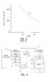
- FIG. 2illustrates a relationship between silicon layer thickness and strain.
- FIG. 3depicts an embodiment of an electronic device using a semiconductor on insulator structure, according to the present invention.
- FIG. 4is a simplified block diagram of a memory device using an embodiment of a semiconductor on insulator structure, according to the present invention.
- FIG. 5illustrates a block diagram for an electronic system having devices that use an embodiment of a semiconductor on insulator structure, according to the present invention.
- FIG. 6illustrates the relationship of elements in an embodiment for a method to form a semiconductor on insulator structure, according to the present invention.
- wafer and substrate used in the following descriptioninclude any structure having an exposed surface with which to form an integrated circuit (IC) structure.
- substrateis understood to include semiconductor wafers. Both wafer and substrate can include doped and undoped semiconductors, epitaxial semiconductor layers supported by a base semiconductor or insulator, as well as other semiconductor structures well known to one skilled in the art.
- FIG. 1illustrates an embodiment of a semiconductor on insulator structure 100 .
- Semiconductor on insulator structure 100includes a glass substrate 105 , and an ultra-thin semiconductor layer 110 bonded to the glass substrate 105 .
- Semiconductor on insulator structure 100is configured with semiconductor layer 105 having a thickness such that semiconductor layer 105 does not yield due to temperature-induced strain at device processing temperatures.
- Temperature-induced strainincludes strain that is produced in a material combined with another material as a result of mismatches in the coefficients of thermal expansion of the two materials.
- an insulator layer 112is disposed between semiconductor layer 110 and glass substrate 105 .
- Insulator layer 112can be an oxide of a semiconductor material contained in semiconductor layer 110 .
- semiconductor layer 110includes a silicon layer.
- insulator layer 112is a silicon oxide, which can include a native silicon oxide.
- insulator layer 112is not limited to an oxide and can include other insulator materials. Insulator layer 112 can provide further reduction of stray capacitances and/or be used in processing device circuitry in the semiconductor on insulator structure.
- semiconductor layer 110can include and is not limited to a semiconductor layer containing germanium, gallium arsenide, a silicon-germanium compound, and other semiconductor materials as are known to those skilled in the art.
- glass substrate 105can be a fused quartz substrate or a fused silica substrate. Alternately, glass substrate 105 includes a borosilicate glass substrate. An embodiment includes a thin silicon layer 110 on a glass substrate 105 , where the glass substrate 105 can include a fused silica substrate, a fused quartz substrate, or a borosilicate glass substrate.
- the use of glass substratesserves to reduce the energy consumption and costs of fabricating a silicon microchip that are typically associated with producing high quality crystalline substrates in which the majority of the silicon substrate is not used in any device function and serves only as a carrier substrate. The use of high quality, high cost crystalline substrates as such a carrier substrate is typically not an efficient use of resources.
- a silicon on insulator structure where the silicon is bonded to a substrateis subject to problems during device formation using varying temperature processes.
- One of the problems associated with temperature processing in a bonded wafer technologyinvolves the difference in coefficients of thermal expansion between the bonded materials.
- the coefficients of thermal expansion for some commonly used materialsincludes silicon carbide with a coefficient of thermal expansion of 4.0 to 3.9 ⁇ 10-6 cm/(cm K), silicon oxide with a coefficient of thermal expansion of 0.5 ⁇ 10-6 cm/(cm K), and silicon with a coefficient of thermal expansion of 2.6 ⁇ 10-6 cm/(cm K).
- FIG. 2provides an example of the limits on strain versus silicon layer thickness, where the dashed line 200 delineates the onset for yield, plastic deformation and defects in bulk silicon samples. If the strain is too large the materials will plastically deform by the introduction of dislocations, fracture and yield, or undergo excessive wafer bowing and/or warping.
- An approach to reduce stressincludes bonding silicon on to compliant substrates using low viscosity borophosphorosilicate glass films, which flows to reduce the stress. Another approach is to use materials where the coefficients of thermal expansion match as closely as possible.
- a semiconductor on insulatorincludes a thin semiconductor layer bonded to a glass substrate, where the thin semiconductor layer has a thickness such that the semiconductor layer does not yield due to temperature-induced strain at device processing temperatures.
- the thin semiconductor layeris an ultra-thin silicon layer having a thickness of 0.1 microns or less bonded to a glass substrate.
- the glass substratecan include fused silica, fused quartz, or a borosilicate glass.
- Fused silica and fused quartzhave a very high UV transmission, an extremely low coefficient of thermal expansion, a high temperature and chemical resistance, low loss dielectric properties, and electrical insulating properties.
- Applications for fused silica or fused quartzinclude optical reference flats, windows, mirrors, test plates, high temperature view ports, optical components, aerospace applications, solar cells, and passive energy collectors.
- These glass materialscan be provided in the form of wafers at costs significantly less than the costs associated with providing high quality, crystalline semiconductor wafers. Thus, application of these materials in semiconductor device processing can reduce the overall cost to manufacture the device.
- FIG. 3depicts an embodiment of an electronic device 300 using a semiconductor on insulator structure.
- Electronic device 300includes a glass substrate 305 , a thin semiconductor layer 310 bonded to glass substrate 305 , where semiconductor layer 310 has a thickness such that the semiconductor layer does not yield due to temperature-induced strain at device processing temperatures, and circuitry in thin semiconductor layer 310 .
- FIG. 3also depicts a transistor having a source 320 , a drain 330 , a gate dielectric 340 disposed between source 320 and drain 330 , and a gate 350 disposed on gate dielectric 340 , where the transistor is an example of the circuitry for an electronic device 300 using a semiconductor on insulator structure.
- An embodiment of an electronic device using a semiconductor on insulator as described hereinis not limited to a transistor, but includes electronic devices using such a semiconductor on insulator structure.
- the circuitry of electronic device 300includes a memory circuit.
- electronic device 300can include an insulating layer 312 between thin semiconductor layer 310 and glass substrate 305 .
- Insulator layer 312can be a oxide of a semiconductor material contained in semiconductor layer 310 .
- semiconductor layer 310includes a silicon layer.
- semiconductor layer 310includes a silicon layer having an insulating layer 312 , where insulator layer 312 is a silicon oxide, which can include a native silicon oxide.
- insulator layer 312is not limited to an oxide and can include other insulator materials.
- semiconductor layer 310can include and is not limited to a semiconductor layer containing silicon, germanium, gallium arsenide, a silicon-germanium compound, and other semiconductor materials as are known to those skilled in the art.
- FIG. 4is a simplified block diagram of a memory device 400 using an embodiment of a semiconductor on insulator structure.
- Memory device 400includes an array of memory cells 402 , address decoder 404 , row access circuitry 406 , column access circuitry 408 , control circuitry 410 , and Input/Output circuit 412 .
- the memoryis operably coupled to an external microprocessor 414 , or memory controller for memory accessing.
- Memory device 400receives control signals from processor 414 , such as WE*, RAS* and CAS* signals, which can be supplied on a system bus.
- Memory device 400stores data that is accessed via I/O lines.
- At least one of the integrated circuit structuresis formed in a silicon layer that is part of a semiconductor on insulator structure, such as a silicon on glass structure, according to an embodiment of the present invention.
- a memory deviceis intended to provide a general understanding of the memory and is not a complete description of all the elements and features of a specific type of memory, such as DRAM (Dynamic Random Access Memory). Further, embodiments are equally applicable to any size and type of memory circuit and are not intended to be limited to the DRAM described above. Other alternative types of devices include SRAM (Static Random Access Memory) or Flash memories.
- the DRAMcould be a synchronous DRAM commonly referred to as SGRAM (Synchronous Graphics Random Access Memory), SDRAM (Synchronous Dynamic Random Access Memory), SDRAM II, and DDR SDRAM (Double Data Rate SDRAM), as well as Synchlink or Rambus DRAMs and other emerging DRAM technologies.
- SGRAMSynchronous Graphics Random Access Memory
- SDRAMSynchronous Dynamic Random Access Memory
- SDRAM IISynchroble Data Rate SDRAM
- DDR SDRAMDouble Data Rate SDRAM
- FIG. 5illustrates a block diagram for an electronic system 500 having devices using an embodiment for a semiconductor on insulator structure.
- Electronic system 500includes a controller 505 , a bus 515 , and an electronic device 525 , where bus 515 provides electrical conductivity between controller 505 and electronic device 525 .
- controller 505 and/or electronic device 525includes an embodiment for a semiconductor on insulator structure as previously discussed having a glass substrate and a thin semiconductor layer bonded to the glass substrate. The thin semiconductor layer has a thickness such that the semiconductor layer does not yield due to temperature-induced strain at device processing temperatures.
- electronic system 500includes a plurality of electronic devices using an embodiment for a semiconductor on insulator structure according to the present invention.
- Electronic system 500may include, but is not limited to, information handling devices, wireless systems, telecommunication systems, fiber optic systems, electro-optic systems, and computers.
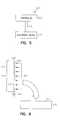
- FIG. 6illustrates the relationship of elements in an embodiment for a method to form a semiconductor on insulator structure according to the present invention.
- An embodiment for a method to form a semiconductor on insulator structureincludes providing a glass substrate, providing a semiconductor wafer, and performing a bonding cut process on the semiconductor wafer and the glass substrate to provide a thin semiconductor layer bonded to the glass substrate.
- the semiconductor layer bonded to the glass substratehas a thickness such that the semiconductor layer does not yield due to temperature-induced strain at device processing temperatures.
- a bonding cut processrefers to a process in which two substrates, or wafers, are bonded together and a section of at least one of the two wafers is cut or broken off after attaching the two wafers together.
- the waferis conditioned prior to the actual cut by implanting atoms to a predetermined distance into the wafer to be cut.
- the attached wafersare heated to cut the conditioned wafers and to bond further the remaining portions of the two wafers at the attachment plane.
- a glass substrate 605 provided for fabricating a semiconductor on insulator structureincludes a substrate of glass material.
- the glass materialcan include fused silica, fused quartz, and borosilicate glass.
- the glass substrateis generated from thin glass sheets.
- the thin glass sheetscan include sheets of fused silica, fused quartz, or borosilicate glass with a very low sodium concentration. These glass sheets are polished and cut into wafer size patterns to act as substrates for integrated circuits. These wafer size glass sheets forming glass substrates are relatively inexpensive as compared with silicon substrates. After patterning the glass substrates, these glass substrates can be further chemically and mechanically polished.
- silicon wafer 615 and glass substrate 605can be cleaned using conventional cleaning procedures.
- silicon wafer 615is also conditioned by forming an oxide on surface 620 before applying a cleaning procedure.
- surface 620 of silicon wafer 615with or without an oxide layer formed thereon, is attached to a surface 610 of glass substrate 605 .
- This attachmentprovides a bonding of silicon wafer 615 to glass substrate 605 , typically by using Van der Walls forces.
- silicon wafer 615is further bonded to glass substrate 605 causing a section 650 of silicon wafer 615 to cut or break off along cleavage plane 640 .
- intermediate silicon layer 630is bonded to glass substrate 605 .
- Intermediate silicon layer 630is defined by the depth of ion implantation to line 640 and has a thin thickness 635 .
- thickness 635is generated to a thickness such that intermediate silicon layer 630 does not yield due to temperature-induced strain at device processing temperatures allowing intermediate silicon layer 630 to be used as the thin semiconductor layer 110 as depicted in FIG. 1.
- intermediate silicon layer 630has a thickness of about 0.1 microns.
- intermediate silicon layer 630has a thickness less than 0.1 microns.
- section 650is relatively thick and has the form of a silicon substrate. Section 650 can be used with another glass substrate to form another silicon on insulator structure, during which fabrication another remaining section from the bond cut process becomes available to be used with yet another glass substrate. This reduces the overall cost for the manufacturing process of a wide variety of electronic devices.
- plasma enhanced bondingis used to bond intermediate silicon layer 630 to glass substrate 605 and cut or break off section 650 .
- the bonding cut processincludes raising the temperature of silicon wafer 615 attached to glass substrate 605 to a temperature ranging from about 400° C. to about 600° C. to cut or break off section 650 . Then, the resulting bond between intermediate silicon layer 630 and glass substrate 605 can be strengthened by raising the temperature to a range from about 800° C. to about 1000° C. or annealing by laser assisted annealing.
- bonding of the silicon wafer 615with or without an oxide layer on surface 620 , can be accomplished with anodic bonding, anodic bonding for a CMOS process introduces high alkali concentration, which is not appropriate for the CMOS process.
- intermediate silicon layer 630that is bonded to glass substrate 605 , with or without an insulating layer between silicon layer 630 and glass substrate 605 , thins intermediate silicon layer 630 .
- This subsequent polishing processesprovides a thin silicon layer for the silicon on insulator structure.
- intermediate silicon layer 630is polished to provide an ultra-thin silicon layer having a thickness of about 0.1 micron.
- intermediate silicon layer 630is polished to provide an ultra-thin silicon layer having a thickness of less than 0.1 microns.
- a silicon on insulator structureis ready for device processing.
- removed section 650can be used to fabricate other silicon on insulator wafers.
- embodimentsinclude other semiconductor materials in place of the silicon to provide a thin semiconductor layer on a glass substrate such that the thin semiconductor layer does not yield due to temperature-induced strain at device processing temperatures. Thermal processing for the bond cut is performed by temperatures appropriate for the semiconductor wafer used.
- CMOS devicescan be fabricated by masking device areas with oxide and nitride and oxidizing the silicon in between device mesas, followed by conventional device fabrication techniques.
- partially depleted CMOS devicescan be formed with or without floating bodies.
- a layer of silicon thicker than for a fully depleted CMOS processis used and the thicker silicon layer is patterned by a trench isolation process similar to a SIMOX process. After patterning the silicon layer by the trench isolation, conventional techniques are used to process the device.
- an isolated silicon device areais realized on an insulating substrate. Stray capacitances are minimized because the device drain, source, and/or collectors are on an insulating glass layer. Interconnection wire is configured over an isolation oxide and the insulating substrate to minimize wiring capacitance. Reducing these parasitic capacitances reduces power consumption during circuit operation and increases the speed of operation.
- a method including the procedures and processes for forming a semiconductor on insulator structure and for forming devices and systems with elements using a semiconductor on insulator structureare controlled by a computer according to the teachings of the present invention.
- the instructions for the methodare stored in a computer readable format on a computer readable media. Examples of such computer readable media include but are not limited to laser readable disks, magnetic disks and tape, and computer memory.
- Embodiments of the present inventioninclude the use of glass substrates that serve to reduce the energy consumption and costs of fabricating a silicon microchip that are typically associated with producing high quality crystalline substrates.
- Performing a bonding cut process on a semiconductor wafer and a glass wafer to form a semiconductor on insulator structure having a thin semiconductor layer in which electronic circuitry can be formedhas several attributes.
- the cost associated with providing glass substratesis significantly less than the cost for providing high quality semiconductor wafers such as silicon wafers.
- Performing a bond cut process as described hereinallows a ultra-thin semiconductor layer to be taken from a high quality semiconductor wafer, such as a silicon wafer, to form a semiconductor on insulator wafer and at the same time provide for use of the same high quality semiconductor wafer to form a plurality of semiconductor on insulator structures.
- semiconductor on insulator wafers formed according to embodiments of the present inventionprovide an isolated device area on an insulating substrate where stray device capacitances and wiring capacitances are minimized. Reducing these parasitic capacitances reduces power consumption during circuit operation and increases the speed of operation.
Landscapes
- Engineering & Computer Science (AREA)
- Physics & Mathematics (AREA)
- Condensed Matter Physics & Semiconductors (AREA)
- General Physics & Mathematics (AREA)
- Manufacturing & Machinery (AREA)
- Computer Hardware Design (AREA)
- Microelectronics & Electronic Packaging (AREA)
- Power Engineering (AREA)
- Element Separation (AREA)
- Thin Film Transistor (AREA)
Abstract
Description
- This application is related to the following commonly assigned U.S. patent application, U.S. application Ser. No. ______ (Attorney Docket No. 1303.098US1), entitled: “Silicon Oxycarbide Glass Substrates for Bonded Silicon on Insulator,” filed ______, which is herein incorporated by reference in its entirety.[0001]
- This application relates generally to electronic devices and device fabrication and, in particular, semiconductor on insulator devices and their fabrication.[0002]
- Almost half the energy expended by a silicon microchip during its manufacture and lifetime is spent in producing the silicon wafer material, and another quarter is spent during the operating lifetime of the microchip. A technique that reduces the energy associated with fabrication of the silicon material and power consumption during operation will reduce the overall cost of the silicon microchip integrated circuit.[0003]
- Power consumption during operation can be reduced using silicon on insulator (SOI) technology. The use of SOI technology not only results in a lower power consumption but also increased speed of operation of integrated circuits due to a reduction in stray capacitance. For SOI structures, thin layers of silicon on insulator can be fabricated using several well known techniques such as separation by implantation of oxygen (SIMOX), separation by plasma implantation of oxygen (SPIMOX), silicon on sapphire (SOS), bonded wafer processes on silicon, and silicon bonded on sapphire.[0004]
- Bonded wafer processes on silicon involve technologies to bond monocrystalline silicon materials onto semiconductor wafers and oxidation processes to form the semiconductor on insulator. In these technologies, a portion of one or both of the bonded wafers is removed, typically, by polishing methods. Another process to remove large portions of a bonded wafer uses a “Smart cut” technology. “Smart cut” technology generally refers to a process in which a material is implanted into a silicon substrate to a particular depth and ultimately utilized to crack the substrate.[0005]
- There continues to be a need to provide fabrication processes and structures to reduce the overall cost for a silicon microchip integrated circuit.[0006]
- The abovementioned problems are addressed by the present invention and will be understood by reading and studying the following specification. An embodiment of a method for forming a semiconductor on insulator structure includes providing a glass substrate, providing a semiconductor substrate, and performing a bonding cut process on the semiconductor wafer and the glass substrate to provide a thin semiconductor layer bonded to the glass substrate. The thin semiconductor layer is formed to a thickness such that it does not yield due to temperature-induced strain at device processing temperatures. In an embodiment, the glass substrate can be a fused silica substrate, a fused quartz substrate, or a borosilicate glass substrate. In an embodiment, a silicon layer bonded to a glass substrate provides a silicon on insulator structure in which circuitry for electronic devices is configured.[0007]
- These and other aspects, embodiments, advantages, and features will become apparent from the following description and the referenced drawings.[0008]
- FIG. 1 illustrates an embodiment of a semiconductor on insulator, according to the present invention.[0009]
- FIG. 2 illustrates a relationship between silicon layer thickness and strain.[0010]
- FIG. 3 depicts an embodiment of an electronic device using a semiconductor on insulator structure, according to the present invention.[0011]
- FIG. 4 is a simplified block diagram of a memory device using an embodiment of a semiconductor on insulator structure, according to the present invention.[0012]
- FIG. 5 illustrates a block diagram for an electronic system having devices that use an embodiment of a semiconductor on insulator structure, according to the present invention.[0013]
- FIG. 6 illustrates the relationship of elements in an embodiment for a method to form a semiconductor on insulator structure, according to the present invention.[0014]
- The following detailed description refers to the accompanying drawings that show, by way of illustration, specific aspects and embodiments in which the present invention may be practiced. These embodiments are described in sufficient detail to enable those skilled in the art to practice the present invention. Other embodiments may be utilized and structural, logical, and electrical changes may be made without departing from the scope of the present invention. The various embodiments disclosed herein are not necessarily mutually exclusive, as some disclosed embodiments can be combined with one or more other disclosed embodiments to form new embodiments.[0015]
- The terms wafer and substrate used in the following description include any structure having an exposed surface with which to form an integrated circuit (IC) structure. The term substrate is understood to include semiconductor wafers. Both wafer and substrate can include doped and undoped semiconductors, epitaxial semiconductor layers supported by a base semiconductor or insulator, as well as other semiconductor structures well known to one skilled in the art.[0016]
- The following detailed description is, therefore, not to be taken in a limiting sense, and the scope of the present invention is defined only by the appended claims, along with the full scope of equivalents to which such claims are entitled.[0017]
- FIG. 1 illustrates an embodiment of a semiconductor on[0018]
insulator structure 100. Semiconductor oninsulator structure 100 includes aglass substrate 105, and an ultra-thin semiconductor layer110 bonded to theglass substrate 105. Semiconductor oninsulator structure 100 is configured withsemiconductor layer 105 having a thickness such thatsemiconductor layer 105 does not yield due to temperature-induced strain at device processing temperatures. Temperature-induced strain includes strain that is produced in a material combined with another material as a result of mismatches in the coefficients of thermal expansion of the two materials. - In an embodiment, an[0019]
insulator layer 112 is disposed between semiconductor layer110 andglass substrate 105.Insulator layer 112 can be an oxide of a semiconductor material contained in semiconductor layer110. In an embodiment, semiconductor layer110 includes a silicon layer. In an embodiment where semiconductor layer110 includes a silicon layer havinginsulator layer 112,insulator layer 112 is a silicon oxide, which can include a native silicon oxide. However,insulator layer 112 is not limited to an oxide and can include other insulator materials.Insulator layer 112 can provide further reduction of stray capacitances and/or be used in processing device circuitry in the semiconductor on insulator structure. Additionally, semiconductor layer110 can include and is not limited to a semiconductor layer containing germanium, gallium arsenide, a silicon-germanium compound, and other semiconductor materials as are known to those skilled in the art. - In an embodiment,[0020]
glass substrate 105 can be a fused quartz substrate or a fused silica substrate. Alternately,glass substrate 105 includes a borosilicate glass substrate. An embodiment includes a thin silicon layer110 on aglass substrate 105, where theglass substrate 105 can include a fused silica substrate, a fused quartz substrate, or a borosilicate glass substrate. The use of glass substrates serves to reduce the energy consumption and costs of fabricating a silicon microchip that are typically associated with producing high quality crystalline substrates in which the majority of the silicon substrate is not used in any device function and serves only as a carrier substrate. The use of high quality, high cost crystalline substrates as such a carrier substrate is typically not an efficient use of resources. - In addition to efficient use of resources, fabrication concerns are associated with processing devices in a wafer at elevated temperatures. For instance, a silicon on insulator structure where the silicon is bonded to a substrate is subject to problems during device formation using varying temperature processes. One of the problems associated with temperature processing in a bonded wafer technology involves the difference in coefficients of thermal expansion between the bonded materials. For example, the coefficients of thermal expansion for some commonly used materials includes silicon carbide with a coefficient of thermal expansion of 4.0 to 3.9×10⁻⁶ cm/(cm K), silicon oxide with a coefficient of thermal expansion of 0.5×10⁻⁶ cm/(cm K), and silicon with a coefficient of thermal expansion of 2.6×10⁻⁶ cm/(cm K). Associated with these differences in the coefficients of thermal expansion is the creation of excessive stress when bonding thick layers when there is a mismatch in the coefficients of thermal expansion. The development of excessive stress can result in exceeding the strain limit of the materials. FIG. 2 provides an example of the limits on strain versus silicon layer thickness, where the[0021]
dashed line 200 delineates the onset for yield, plastic deformation and defects in bulk silicon samples. If the strain is too large the materials will plastically deform by the introduction of dislocations, fracture and yield, or undergo excessive wafer bowing and/or warping. An approach to reduce stress includes bonding silicon on to compliant substrates using low viscosity borophosphorosilicate glass films, which flows to reduce the stress. Another approach is to use materials where the coefficients of thermal expansion match as closely as possible. - In embodiments according to the present invention, a semiconductor on insulator includes a thin semiconductor layer bonded to a glass substrate, where the thin semiconductor layer has a thickness such that the semiconductor layer does not yield due to temperature-induced strain at device processing temperatures. In an embodiment, the thin semiconductor layer is an ultra-thin silicon layer having a thickness of 0.1 microns or less bonded to a glass substrate. The glass substrate can include fused silica, fused quartz, or a borosilicate glass. These thin layers of 0.1 microns or less can tolerate the strain introduced by thermal cycling and the differences in thermal expansion coefficients. A 1000° C. temperature difference will only produce a strain of about 0.21%, which, as shown in FIG. 2, is not sufficient to cause the thin silicon layer to yield.[0022]
- Fused silica and fused quartz have a very high UV transmission, an extremely low coefficient of thermal expansion, a high temperature and chemical resistance, low loss dielectric properties, and electrical insulating properties. Applications for fused silica or fused quartz include optical reference flats, windows, mirrors, test plates, high temperature view ports, optical components, aerospace applications, solar cells, and passive energy collectors.[0023]
- One generally known and commonly used borosilicate glass having a low coefficient of expansion, which has typically been used for heat-resistant glassware in cooking and chemistry, is PYREX. PYREX has a low coefficient of thermal expansion, a high chemical, acid and temperature resistance, and high energy transmission properties with wider spectral band than soda lime in both infrared and ultraviolet ranges. PYREX is used for dielectric coating substrates, neutron absorbers, and in high temperature, long-term, extreme environmental applications. Embodiments of the present invention include PYREX material as a glass substrate for semiconductor on insulator structures.[0024]
- These glass materials can be provided in the form of wafers at costs significantly less than the costs associated with providing high quality, crystalline semiconductor wafers. Thus, application of these materials in semiconductor device processing can reduce the overall cost to manufacture the device.[0025]
- In embodiments, devices using the semiconductor on insulator structure of the present invention include circuitry in a thin semiconductor layer. In an embodiment, the circuitry is configured in a thin silicon layer bonded to a glass substrate. The thin silicon layer is monocrystalline allowing circuitry in the silicon layer, such as transistors, to have the performance level associated with devices having structures using single crystalline form. Having devices using single crystalline structures avoids the problems associated with grain boundaries of polycrystalline devices such as thin film polycrystalline transistors.[0026]
- FIG. 3 depicts an embodiment of an[0027]
electronic device 300 using a semiconductor on insulator structure.Electronic device 300 includes aglass substrate 305, a thin semiconductor layer310 bonded toglass substrate 305, where semiconductor layer310 has a thickness such that the semiconductor layer does not yield due to temperature-induced strain at device processing temperatures, and circuitry in thin semiconductor layer310. FIG. 3 also depicts a transistor having asource 320, adrain 330, agate dielectric 340 disposed betweensource 320 and drain330, and agate 350 disposed ongate dielectric 340, where the transistor is an example of the circuitry for anelectronic device 300 using a semiconductor on insulator structure. An embodiment of an electronic device using a semiconductor on insulator as described herein is not limited to a transistor, but includes electronic devices using such a semiconductor on insulator structure. In an embodiment, the circuitry ofelectronic device 300 includes a memory circuit. - In an embodiment for electronic device, in addition to insulating[0028]
glass substrate 305,electronic device 300 can include an insulatinglayer 312 between thin semiconductor layer310 andglass substrate 305.Insulator layer 312 can be a oxide of a semiconductor material contained in semiconductor layer310. In an embodiment, semiconductor layer310 includes a silicon layer. In an embodiment, semiconductor layer310 includes a silicon layer having an insulatinglayer 312, whereinsulator layer 312 is a silicon oxide, which can include a native silicon oxide. However,insulator layer 312 is not limited to an oxide and can include other insulator materials. Additionally, semiconductor layer310 can include and is not limited to a semiconductor layer containing silicon, germanium, gallium arsenide, a silicon-germanium compound, and other semiconductor materials as are known to those skilled in the art. - In an embodiment,[0029]
glass substrate 305 includes a fused quartz substrate or a fused silica substrate. Alternately,glass substrate 305 includes a borosilicate glass substrate. An embodiment includes a thin silicon layer310 on aglass substrate 305, where theglass substrate 305 includes a fused silica substrate, a fused quartz substrate, or a borosilicate glass substrate. - Various embodiments of[0030]
electronic device 300 include fully depleted devices using CMOS device technology, and various embodiments include partially depleted devices. Devices using a partially depleted CMOS process can be configured with or without floating bodies. The structure, formation, and operation of CMOS devices are understood by those skilled in the art. - Embodiments for electronic devices using semiconductor on insulator structures as described herein have an isolated device area realized on an insulating substrate. Stray capacitances are minimized because the device drain, source, and/or collectors are on an insulating glass layer. Interconnection wire is configured over an isolation oxide and the insulating substrate to minimize wiring capacitance. Reducing these parasitic capacitances reduces power consumption during circuit operation and increases the speed of operation.[0031]
- FIG. 4 is a simplified block diagram of a[0032]
memory device 400 using an embodiment of a semiconductor on insulator structure.Memory device 400 includes an array ofmemory cells 402,address decoder 404,row access circuitry 406,column access circuitry 408,control circuitry 410, and Input/Output circuit 412. The memory is operably coupled to anexternal microprocessor 414, or memory controller for memory accessing.Memory device 400 receives control signals fromprocessor 414, such as WE*, RAS* and CAS* signals, which can be supplied on a system bus.Memory device 400 stores data that is accessed via I/O lines. It will be appreciated by those skilled in the art that additional circuitry and control signals can be provided, and that the memory device of FIG. 4 has been simplified to help focus on the present invention. At least one of the integrated circuit structures is formed in a silicon layer that is part of a semiconductor on insulator structure, such as a silicon on glass structure, according to an embodiment of the present invention. - It will be understood that the above description of a memory device is intended to provide a general understanding of the memory and is not a complete description of all the elements and features of a specific type of memory, such as DRAM (Dynamic Random Access Memory). Further, embodiments are equally applicable to any size and type of memory circuit and are not intended to be limited to the DRAM described above. Other alternative types of devices include SRAM (Static Random Access Memory) or Flash memories. Additionally, the DRAM could be a synchronous DRAM commonly referred to as SGRAM (Synchronous Graphics Random Access Memory), SDRAM (Synchronous Dynamic Random Access Memory), SDRAM II, and DDR SDRAM (Double Data Rate SDRAM), as well as Synchlink or Rambus DRAMs and other emerging DRAM technologies.[0033]
- FIG. 5 illustrates a block diagram for an[0034]
electronic system 500 having devices using an embodiment for a semiconductor on insulator structure.Electronic system 500 includes acontroller 505, a bus515, and anelectronic device 525, where bus515 provides electrical conductivity betweencontroller 505 andelectronic device 525. In various embodiments,controller 505 and/orelectronic device 525 includes an embodiment for a semiconductor on insulator structure as previously discussed having a glass substrate and a thin semiconductor layer bonded to the glass substrate. The thin semiconductor layer has a thickness such that the semiconductor layer does not yield due to temperature-induced strain at device processing temperatures. In an embodiment,electronic system 500 includes a plurality of electronic devices using an embodiment for a semiconductor on insulator structure according to the present invention.Electronic system 500 may include, but is not limited to, information handling devices, wireless systems, telecommunication systems, fiber optic systems, electro-optic systems, and computers. - FIG. 6 illustrates the relationship of elements in an embodiment for a method to form a semiconductor on insulator structure according to the present invention. An embodiment for a method to form a semiconductor on insulator structure includes providing a glass substrate, providing a semiconductor wafer, and performing a bonding cut process on the semiconductor wafer and the glass substrate to provide a thin semiconductor layer bonded to the glass substrate. The semiconductor layer bonded to the glass substrate has a thickness such that the semiconductor layer does not yield due to temperature-induced strain at device processing temperatures.[0035]
- Herein, a bonding cut process refers to a process in which two substrates, or wafers, are bonded together and a section of at least one of the two wafers is cut or broken off after attaching the two wafers together. For each wafer for which a section is cut or broken off, the wafer is conditioned prior to the actual cut by implanting atoms to a predetermined distance into the wafer to be cut. The attached wafers are heated to cut the conditioned wafers and to bond further the remaining portions of the two wafers at the attachment plane. The section removed from a conditioned wafer is the section of the conditioned wafer from the end of the conditioned wafer, which is away from the attachment to the other wafer, to the plane along the conditioned wafer that is at the distance to which the implantation was made. The removed section includes a significant portion of the original wafer, with the smaller portion that was subjected to implantation remaining bonded to the other wafer.[0036]
- In an embodiment, a glass substrate[0037]605 provided for fabricating a semiconductor on insulator structure includes a substrate of glass material. The glass material can include fused silica, fused quartz, and borosilicate glass. In an embodiment, the glass substrate is generated from thin glass sheets. The thin glass sheets can include sheets of fused silica, fused quartz, or borosilicate glass with a very low sodium concentration. These glass sheets are polished and cut into wafer size patterns to act as substrates for integrated circuits. These wafer size glass sheets forming glass substrates are relatively inexpensive as compared with silicon substrates. After patterning the glass substrates, these glass substrates can be further chemically and mechanically polished.
- [0038]
Semiconductor wafer 615 is conditioned as part of the bonding cut process prior to bonding to glass substrate605.Semiconductor wafer 615 can include wafers having semiconductor material that includes, but is not limited to, silicon, germanium, silicon-germanium, gallium arsenide, indium phosphide, and other semiconductor materials. For ease of discussion regarding embodiments according to the present invention, the remainder of this discussion focuses on an embodiment using a silicon wafer assemiconductor wafer 615. - [0039]
Silicon wafer 615, a single crystal wafer, is conditioned by subjecting asurface 620 to implantation ofions 625 to form anintermediate silicon layer 630 having athickness 635. The ions are implanted along aplane 640, represented in FIG. 6 as a line, which is approximately parallel tosurface 620. In an embodiment, hydrogen ions are used asimplantation ions 625. The hydrogen ions can take the form of H+, H2+, D+, or D2+ ions. The implanted ions act to form cavities along thecleavage plane 640. The cavities are joined through thermal processing. Once these cavities join, the wafer becomes cut or broken off alongplane 640. In an embodiment,silicon wafer 615 is also conditioned by forming an oxide onsurface 620. The oxide can include a native oxide. The ion implantation can be performed before or after the oxide formation. - After[0040]
conditioning silicon wafer 615,silicon wafer 615 and glass substrate605 can be cleaned using conventional cleaning procedures. In an embodiment,silicon wafer 615 is also conditioned by forming an oxide onsurface 620 before applying a cleaning procedure. Then,surface 620 ofsilicon wafer 615, with or without an oxide layer formed thereon, is attached to asurface 610 of glass substrate605. This attachment provides a bonding ofsilicon wafer 615 to glass substrate605, typically by using Van der Walls forces. Then,silicon wafer 615 is further bonded to glass substrate605 causing asection 650 ofsilicon wafer 615 to cut or break off alongcleavage plane 640. - As a result of this bonding cut,[0041]
intermediate silicon layer 630 is bonded to glass substrate605.Intermediate silicon layer 630 is defined by the depth of ion implantation toline 640 and has athin thickness 635. In an embodiment,thickness 635 is generated to a thickness such thatintermediate silicon layer 630 does not yield due to temperature-induced strain at device processing temperatures allowingintermediate silicon layer 630 to be used as the thin semiconductor layer110 as depicted in FIG. 1. In an embodiment,intermediate silicon layer 630 has a thickness of about 0.1 microns. In an embodiment,intermediate silicon layer 630 has a thickness less than 0.1 microns. As a result of the thin nature ofintermediate silicon layer 630,section 650 is relatively thick and has the form of a silicon substrate.Section 650 can be used with another glass substrate to form another silicon on insulator structure, during which fabrication another remaining section from the bond cut process becomes available to be used with yet another glass substrate. This reduces the overall cost for the manufacturing process of a wide variety of electronic devices. - In an embodiment, plasma enhanced bonding is used to bond[0042]
intermediate silicon layer 630 to glass substrate605 and cut or break offsection 650. In an embodiment, the bonding cut process includes raising the temperature ofsilicon wafer 615 attached to glass substrate605 to a temperature ranging from about 400° C. to about 600° C. to cut or break offsection 650. Then, the resulting bond betweenintermediate silicon layer 630 and glass substrate605 can be strengthened by raising the temperature to a range from about 800° C. to about 1000° C. or annealing by laser assisted annealing. Though bonding of thesilicon wafer 615, with or without an oxide layer onsurface 620, can be accomplished with anodic bonding, anodic bonding for a CMOS process introduces high alkali concentration, which is not appropriate for the CMOS process. - In an embodiment, polishing[0043]
intermediate silicon layer 630 that is bonded to glass substrate605, with or without an insulating layer betweensilicon layer 630 and glass substrate605, thinsintermediate silicon layer 630. This subsequent polishing processes provides a thin silicon layer for the silicon on insulator structure. In an embodiment,intermediate silicon layer 630 is polished to provide an ultra-thin silicon layer having a thickness of about 0.1 micron. In an embodiment,intermediate silicon layer 630 is polished to provide an ultra-thin silicon layer having a thickness of less than 0.1 microns. - Once the bond cut process is concluded providing an ultra-thin silicon layer bonded to a glass substrate, a silicon on insulator structure is ready for device processing. Further, removed[0044]
section 650 can be used to fabricate other silicon on insulator wafers. As previously discussed, embodiments include other semiconductor materials in place of the silicon to provide a thin semiconductor layer on a glass substrate such that the thin semiconductor layer does not yield due to temperature-induced strain at device processing temperatures. Thermal processing for the bond cut is performed by temperatures appropriate for the semiconductor wafer used. - Once the semiconductor on insulator wafer has been formed, device processing can be accomplished using conventional processes and procedures. For example, silicon on glass substrates formed according to the present invention can be further processed in a manner similar to silicon-on-sapphire wafers. In an embodiment, fully depleted CMOS devices can be fabricated by masking device areas with oxide and nitride and oxidizing the silicon in between device mesas, followed by conventional device fabrication techniques.[0045]
- In an embodiment for forming an electronic device using a silicon on insulator structure according to the present invention, partially depleted CMOS devices can be formed with or without floating bodies. A layer of silicon thicker than for a fully depleted CMOS process is used and the thicker silicon layer is patterned by a trench isolation process similar to a SIMOX process. After patterning the silicon layer by the trench isolation, conventional techniques are used to process the device.[0046]
- In embodiments using a semiconductor on insulator structure as described herein, an isolated silicon device area is realized on an insulating substrate. Stray capacitances are minimized because the device drain, source, and/or collectors are on an insulating glass layer. Interconnection wire is configured over an isolation oxide and the insulating substrate to minimize wiring capacitance. Reducing these parasitic capacitances reduces power consumption during circuit operation and increases the speed of operation.[0047]
- In an embodiment, a method including the procedures and processes for forming a semiconductor on insulator structure and for forming devices and systems with elements using a semiconductor on insulator structure are controlled by a computer according to the teachings of the present invention. The instructions for the method are stored in a computer readable format on a computer readable media. Examples of such computer readable media include but are not limited to laser readable disks, magnetic disks and tape, and computer memory.[0048]
- Use of silicon substrates as a carrier substrate in which the majority of the silicon substrate is not used in any device function is not an efficient use of resources. Embodiments of the present invention include the use of glass substrates that serve to reduce the energy consumption and costs of fabricating a silicon microchip that are typically associated with producing high quality crystalline substrates. Performing a bonding cut process on a semiconductor wafer and a glass wafer to form a semiconductor on insulator structure having a thin semiconductor layer in which electronic circuitry can be formed has several attributes. By bonding to a glass substrate a semiconductor layer having a thickness such that the semiconductor layer does not yield due to temperature-induced strain at device processing temperatures, problems associated with differences in the coefficient of thermal expansion can be avoided. The cost associated with providing glass substrates is significantly less than the cost for providing high quality semiconductor wafers such as silicon wafers. Performing a bond cut process as described herein allows a ultra-thin semiconductor layer to be taken from a high quality semiconductor wafer, such as a silicon wafer, to form a semiconductor on insulator wafer and at the same time provide for use of the same high quality semiconductor wafer to form a plurality of semiconductor on insulator structures. Further, such semiconductor on insulator wafers formed according to embodiments of the present invention provide an isolated device area on an insulating substrate where stray device capacitances and wiring capacitances are minimized. Reducing these parasitic capacitances reduces power consumption during circuit operation and increases the speed of operation.[0049]
- Although specific embodiments have been illustrated and described herein, it will be appreciated by those of ordinary skill in the art that any arrangement that is calculated to achieve the same purpose may be substituted for the specific embodiments shown. This application is intended to cover any adaptations or variations of the present invention. It is to be understood that the above description is intended to be illustrative, and not restrictive. Combinations of the above embodiments, and other embodiments will be apparent to those of skill in the art upon reviewing the above description. The scope of the present invention includes any other applications in which the above structures and fabrication methods are used. The scope of the present invention should be determined with reference to the appended claims, along with the full scope of equivalents to which such claims are entitled.[0050]
Claims (71)
Priority Applications (3)
| Application Number | Priority Date | Filing Date | Title |
|---|---|---|---|
| US10/443,340US7273788B2 (en) | 2003-05-21 | 2003-05-21 | Ultra-thin semiconductors bonded on glass substrates |
| US10/931,553US7271445B2 (en) | 2003-05-21 | 2004-08-31 | Ultra-thin semiconductors bonded on glass substrates |
| US11/493,128US7504310B2 (en) | 2003-05-21 | 2006-07-26 | Semiconductors bonded on glass substrates |
Applications Claiming Priority (1)
| Application Number | Priority Date | Filing Date | Title |
|---|---|---|---|
| US10/443,340US7273788B2 (en) | 2003-05-21 | 2003-05-21 | Ultra-thin semiconductors bonded on glass substrates |
Related Child Applications (2)
| Application Number | Title | Priority Date | Filing Date |
|---|---|---|---|
| US10/931,553DivisionUS7271445B2 (en) | 2003-05-21 | 2004-08-31 | Ultra-thin semiconductors bonded on glass substrates |
| US11/493,128DivisionUS7504310B2 (en) | 2003-05-21 | 2006-07-26 | Semiconductors bonded on glass substrates |
Publications (2)
| Publication Number | Publication Date |
|---|---|
| US20040232487A1true US20040232487A1 (en) | 2004-11-25 |
| US7273788B2 US7273788B2 (en) | 2007-09-25 |
Family
ID=33450387
Family Applications (3)
| Application Number | Title | Priority Date | Filing Date |
|---|---|---|---|
| US10/443,340Expired - LifetimeUS7273788B2 (en) | 2003-05-21 | 2003-05-21 | Ultra-thin semiconductors bonded on glass substrates |
| US10/931,553Expired - LifetimeUS7271445B2 (en) | 2003-05-21 | 2004-08-31 | Ultra-thin semiconductors bonded on glass substrates |
| US11/493,128Expired - LifetimeUS7504310B2 (en) | 2003-05-21 | 2006-07-26 | Semiconductors bonded on glass substrates |
Family Applications After (2)
| Application Number | Title | Priority Date | Filing Date |
|---|---|---|---|
| US10/931,553Expired - LifetimeUS7271445B2 (en) | 2003-05-21 | 2004-08-31 | Ultra-thin semiconductors bonded on glass substrates |
| US11/493,128Expired - LifetimeUS7504310B2 (en) | 2003-05-21 | 2006-07-26 | Semiconductors bonded on glass substrates |
Country Status (1)
| Country | Link |
|---|---|
| US (3) | US7273788B2 (en) |
Cited By (21)
| Publication number | Priority date | Publication date | Assignee | Title |
|---|---|---|---|---|
| US20040217896A1 (en)* | 2003-01-24 | 2004-11-04 | Stmicroelectronics S.R.L | Multistage analog-to-digital converter |
| US20040217391A1 (en)* | 2003-04-29 | 2004-11-04 | Micron Technology, Inc. | Localized strained semiconductor on insulator |
| US20040221792A1 (en)* | 2003-05-07 | 2004-11-11 | Micron Technology, Inc. | Strained Si/SiGe structures by ion implantation |
| US20040224480A1 (en)* | 2003-05-07 | 2004-11-11 | Micron Technology, Inc. | Micromechanical strained semiconductor by wafer bonding |
| US20060011982A1 (en)* | 2003-03-05 | 2006-01-19 | Micron Technology, Inc. | Micro-mechanically strained semiconductor film |
| US7008854B2 (en) | 2003-05-21 | 2006-03-07 | Micron Technology, Inc. | Silicon oxycarbide substrates for bonded silicon on insulator |
| US20060097281A1 (en)* | 2003-04-29 | 2006-05-11 | Micron Technology, Inc. | Strained semiconductor by wafer bonding with misorientation |
| US7153753B2 (en) | 2003-08-05 | 2006-12-26 | Micron Technology, Inc. | Strained Si/SiGe/SOI islands and processes of making same |
| US7271445B2 (en) | 2003-05-21 | 2007-09-18 | Micron Technology, Inc. | Ultra-thin semiconductors bonded on glass substrates |
| US20080029832A1 (en)* | 2006-08-03 | 2008-02-07 | Micron Technology, Inc. | Bonded strained semiconductor with a desired surface orientation and conductance direction |
| US20080029840A1 (en)* | 2006-08-02 | 2008-02-07 | Micron Technology, Inc. | Strained semiconductor, devices and systems and methods of formation |
| US20080042211A1 (en)* | 2006-08-18 | 2008-02-21 | Micron Technology, Inc. | Strained semiconductor channels and methods of formation |
| US20080233725A1 (en)* | 2007-03-23 | 2008-09-25 | Micron Technology, Inc. | Methods for stressing semiconductor material structures to improve electron and/or hole mobility of transistor channels fabricated therefrom, and semiconductor devices including such structures |
| US7439158B2 (en) | 2003-07-21 | 2008-10-21 | Micron Technology, Inc. | Strained semiconductor by full wafer bonding |
| US20080277734A1 (en)* | 2007-05-08 | 2008-11-13 | Micron Technology, Inc. | Implantation processes for straining transistor channels of semiconductor device structures and semiconductor devices with strained transistor channels |
| US7501329B2 (en) | 2003-05-21 | 2009-03-10 | Micron Technology, Inc. | Wafer gettering using relaxed silicon germanium epitaxial proximity layers |
| US7662701B2 (en) | 2003-05-21 | 2010-02-16 | Micron Technology, Inc. | Gettering of silicon on insulator using relaxed silicon germanium epitaxial proximity layers |
| US8227309B2 (en) | 2006-02-16 | 2012-07-24 | Micron Technology, Inc. | Localized compressive strained semiconductor |
| US20140332934A1 (en)* | 2011-12-16 | 2014-11-13 | Element Six Limited | Substrates for semiconductor devices |
| US20170317171A1 (en)* | 2015-07-30 | 2017-11-02 | International Business Machines Corporation | Leakage-free implantation-free etsoi transistors |
| CN113013061A (en)* | 2021-02-23 | 2021-06-22 | 绍兴同芯成集成电路有限公司 | Method for processing compound semiconductor by using organic film |
Families Citing this family (31)
| Publication number | Priority date | Publication date | Assignee | Title |
|---|---|---|---|---|
| US7057256B2 (en) | 2001-05-25 | 2006-06-06 | President & Fellows Of Harvard College | Silicon-based visible and near-infrared optoelectric devices |
| US7442629B2 (en) | 2004-09-24 | 2008-10-28 | President & Fellows Of Harvard College | Femtosecond laser-induced formation of submicrometer spikes on a semiconductor substrate |
| US7132348B2 (en)* | 2002-03-25 | 2006-11-07 | Micron Technology, Inc. | Low k interconnect dielectric using surface transformation |
| US7274007B2 (en)* | 2003-09-25 | 2007-09-25 | W.E.T. Automotive Systems Ltd. | Control system for operating automotive vehicle components |
| JP4473715B2 (en)* | 2004-11-29 | 2010-06-02 | 富士通株式会社 | LAMINATE CUTTING METHOD AND LAMINATE |
| US7642205B2 (en)* | 2005-04-08 | 2010-01-05 | Mattson Technology, Inc. | Rapid thermal processing using energy transfer layers |
| US8309685B2 (en)* | 2007-12-21 | 2012-11-13 | Celgene Avilomics Research, Inc. | HCV protease inhibitors and uses thereof |
| US7749884B2 (en)* | 2008-05-06 | 2010-07-06 | Astrowatt, Inc. | Method of forming an electronic device using a separation-enhancing species |
| JP2011521456A (en)* | 2008-05-17 | 2011-07-21 | アストロワット,インコーポレイティド | Method for manufacturing electronic device using separation technique |
| KR101525498B1 (en) | 2008-12-04 | 2015-06-03 | 삼성전자주식회사 | Semiconductor device and method of fabricating the same |
| US7927975B2 (en) | 2009-02-04 | 2011-04-19 | Micron Technology, Inc. | Semiconductor material manufacture |
| WO2010109712A1 (en)* | 2009-03-25 | 2010-09-30 | シャープ株式会社 | Insulating substrate for semiconductor device, and semiconductor device |
| US9673243B2 (en) | 2009-09-17 | 2017-06-06 | Sionyx, Llc | Photosensitive imaging devices and associated methods |
| US9911781B2 (en) | 2009-09-17 | 2018-03-06 | Sionyx, Llc | Photosensitive imaging devices and associated methods |
| US8692198B2 (en) | 2010-04-21 | 2014-04-08 | Sionyx, Inc. | Photosensitive imaging devices and associated methods |
| WO2011160130A2 (en) | 2010-06-18 | 2011-12-22 | Sionyx, Inc | High speed photosensitive devices and associated methods |
| US8455308B2 (en) | 2011-03-16 | 2013-06-04 | International Business Machines Corporation | Fully-depleted SON |
| US9496308B2 (en) | 2011-06-09 | 2016-11-15 | Sionyx, Llc | Process module for increasing the response of backside illuminated photosensitive imagers and associated methods |
| WO2013010127A2 (en) | 2011-07-13 | 2013-01-17 | Sionyx, Inc. | Biometric imaging devices and associated methods |
| US20130168803A1 (en)* | 2011-09-16 | 2013-07-04 | Sionyx, Inc. | Semiconductor-On-Insulator Devices and Associated Methods |
| US9064764B2 (en) | 2012-03-22 | 2015-06-23 | Sionyx, Inc. | Pixel isolation elements, devices, and associated methods |
| US8962224B2 (en)* | 2012-08-13 | 2015-02-24 | Applied Materials, Inc. | Methods for controlling defects for extreme ultraviolet lithography (EUVL) photomask substrate |
| US9762830B2 (en) | 2013-02-15 | 2017-09-12 | Sionyx, Llc | High dynamic range CMOS image sensor having anti-blooming properties and associated methods |
| WO2014151093A1 (en) | 2013-03-15 | 2014-09-25 | Sionyx, Inc. | Three dimensional imaging utilizing stacked imager devices and associated methods |
| US9209345B2 (en) | 2013-06-29 | 2015-12-08 | Sionyx, Inc. | Shallow trench textured regions and associated methods |
| US9784917B2 (en) | 2015-10-05 | 2017-10-10 | International Business Machines Corporation | Low-loss large-grain optical waveguide for interconnecting components integrated on a glass substrate |
| US10349613B2 (en)* | 2016-08-17 | 2019-07-16 | Technologies Holdings Corp. | Vision system for teat detection |
| US10499609B2 (en)* | 2016-08-17 | 2019-12-10 | Technologies Holdings Corp. | Vision system for teat detection |
| US10349615B2 (en)* | 2016-08-17 | 2019-07-16 | Technologies Holdings Corp. | Vision system for teat detection |
| WO2018035286A1 (en)* | 2016-08-18 | 2018-02-22 | Corning Incorporated | Laser system and method forming a high purity fused silica glass sheet with micro-crenellations |
| US11274056B2 (en) | 2016-08-24 | 2022-03-15 | Corning Incorporated | Laser system and method forming a high purity fused silica glass sheet with micro-crenellations |
Citations (83)
| Publication number | Priority date | Publication date | Assignee | Title |
|---|---|---|---|---|
| US601711A (en)* | 1898-04-05 | Carpet cleaner | ||
| US4314595A (en)* | 1979-01-19 | 1982-02-09 | Vlsi Technology Research Association | Method of forming nondefective zone in silicon single crystal wafer by two stage-heat treatment |
| US4523975A (en)* | 1982-04-19 | 1985-06-18 | Mitel Corporation | Integrated circuit planarizing process |
| US4589928A (en)* | 1984-08-21 | 1986-05-20 | At&T Bell Laboratories | Method of making semiconductor integrated circuits having backside gettered with phosphorus |
| US4717681A (en)* | 1986-05-19 | 1988-01-05 | Texas Instruments Incorporated | Method of making a heterojunction bipolar transistor with SIPOS |
| US5027101A (en)* | 1987-01-22 | 1991-06-25 | Morrill Jr Vaughan | Sub-miniature fuse |
| US5098852A (en)* | 1989-07-05 | 1992-03-24 | Kabushiki Kaisha Toshiba | Method of manufacturing a semiconductor device by mega-electron volt ion implantation |
| US5426061A (en)* | 1994-09-06 | 1995-06-20 | Midwest Research Institute | Impurity gettering in semiconductors |
| US5482869A (en)* | 1993-03-01 | 1996-01-09 | Kabushiki Kaisha Toshiba | Gettering of unwanted metal impurity introduced into semiconductor substrate during trench formation |
| US5487999A (en)* | 1991-06-04 | 1996-01-30 | Micron Technology, Inc. | Method for fabricating a penetration limited contact having a rough textured surface |
| US5526449A (en)* | 1993-01-08 | 1996-06-11 | Massachusetts Institute Of Technology | Optoelectronic integrated circuits and method of fabricating and reducing losses using same |
| US5646053A (en)* | 1995-12-20 | 1997-07-08 | International Business Machines Corporation | Method and structure for front-side gettering of silicon-on-insulator substrates |
| US5735949A (en)* | 1990-09-13 | 1998-04-07 | Forschungszentrum Julich Gmbh | Method of producing electronic, electrooptical and optical components |
| US5739796A (en)* | 1995-10-30 | 1998-04-14 | The United States Of America As Represented By The Secretary Of The Army | Ultra-wideband photonic band gap crystal having selectable and controllable bad gaps and methods for achieving photonic band gaps |
| US5759898A (en)* | 1993-10-29 | 1998-06-02 | International Business Machines Corporation | Production of substrate for tensilely strained semiconductor |
| US5773152A (en)* | 1994-10-13 | 1998-06-30 | Nec Corporation | SOI substrate having a high heavy metal gettering effect for semiconductor device |
| US5858819A (en)* | 1994-06-15 | 1999-01-12 | Seiko Epson Corporation | Fabrication method for a thin film semiconductor device, the thin film semiconductor device itself, liquid crystal display, and electronic device |
| US5877070A (en)* | 1997-05-31 | 1999-03-02 | Max-Planck Society | Method for the transfer of thin layers of monocrystalline material to a desirable substrate |
| US5879996A (en)* | 1996-09-18 | 1999-03-09 | Micron Technology, Inc. | Silicon-germanium devices for CMOS formed by ion implantation and solid phase epitaxial regrowth |
| US5926740A (en)* | 1997-10-27 | 1999-07-20 | Micron Technology, Inc. | Graded anti-reflective coating for IC lithography |
| US6022793A (en)* | 1997-10-21 | 2000-02-08 | Seh America, Inc. | Silicon and oxygen ion co-implantation for metallic gettering in epitaxial wafers |
| US6028436A (en)* | 1997-12-02 | 2000-02-22 | Micron Technology, Inc. | Method for forming coaxial silicon interconnects |
| US6049106A (en)* | 1999-01-14 | 2000-04-11 | Micron Technology, Inc. | Large grain single crystal vertical thin film polysilicon MOSFETs |
| US6054808A (en)* | 1997-03-19 | 2000-04-25 | Micron Technology, Inc. | Display device with grille having getter material |
| US6075640A (en)* | 1997-11-26 | 2000-06-13 | Massachusetts Institute Of Technology | Signal processing by optically manipulating polaritons |
| US6077792A (en)* | 1997-07-14 | 2000-06-20 | Micron Technology, Inc. | Method of forming foamed polymeric material for an integrated circuit |
| US6083324A (en)* | 1998-02-19 | 2000-07-04 | Silicon Genesis Corporation | Gettering technique for silicon-on-insulator wafers |
| US6093623A (en)* | 1998-08-04 | 2000-07-25 | Micron Technology, Inc. | Methods for making silicon-on-insulator structures |
| US6093624A (en)* | 1997-12-23 | 2000-07-25 | Philips Electronics North America Corporation | Method of providing a gettering scheme in the manufacture of silicon-on-insulator (SOI) integrated circuits |
| US6172456B1 (en)* | 1995-02-10 | 2001-01-09 | Micron Technology, Inc. | Field emission display |
| US6174784B1 (en)* | 1996-09-04 | 2001-01-16 | Micron Technology, Inc. | Technique for producing small islands of silicon on insulator |
| US6180487B1 (en)* | 1999-10-25 | 2001-01-30 | Advanced Micro Devices, Inc. | Selective thinning of barrier oxide through masked SIMOX implant |
| US6204145B1 (en)* | 1996-11-12 | 2001-03-20 | Micron Technology, Inc. | Silicon-on-insulator islands and method for their formation |
| US6228694B1 (en)* | 1999-06-28 | 2001-05-08 | Intel Corporation | Method of increasing the mobility of MOS transistors by use of localized stress regions |
| US6251751B1 (en)* | 1997-10-16 | 2001-06-26 | International Business Machines Corporation | Bulk and strained silicon on insulator using local selective oxidation |
| US6261876B1 (en)* | 1999-11-04 | 2001-07-17 | International Business Machines Corporation | Planar mixed SOI-bulk substrate for microelectronic applications |
| US6338805B1 (en)* | 1999-07-14 | 2002-01-15 | Memc Electronic Materials, Inc. | Process for fabricating semiconductor wafers with external gettering |
| US6339011B1 (en)* | 2001-03-05 | 2002-01-15 | Micron Technology, Inc. | Method of forming semiconductive active area having a proximity gettering region therein and method of processing a monocrystalline silicon substrate to have a proximity gettering region |
| US6351028B1 (en)* | 1999-02-08 | 2002-02-26 | Micron Technology, Inc. | Multiple die stack apparatus employing T-shaped interposer elements |
| US6368938B1 (en)* | 1999-10-05 | 2002-04-09 | Silicon Wafer Technologies, Inc. | Process for manufacturing a silicon-on-insulator substrate and semiconductor devices on said substrate |
| US6376336B1 (en)* | 2001-02-01 | 2002-04-23 | Advanced Micro Devices, Inc. | Frontside SOI gettering with phosphorus doping |
| US6377070B1 (en)* | 2001-02-09 | 2002-04-23 | Micron Technology, Inc. | In-service programmable logic arrays with ultra thin vertical body transistors |
| US20020048969A1 (en)* | 2000-10-23 | 2002-04-25 | Applied Materials, Inc. | Method of forming film, method of manufacturing semiconductor device, and film forming apparatus |
| US6383924B1 (en)* | 2000-12-13 | 2002-05-07 | Micron Technology, Inc. | Method of forming buried conductor patterns by surface transformation of empty spaces in solid state materials |
| US6387732B1 (en)* | 1999-06-18 | 2002-05-14 | Micron Technology, Inc. | Methods of attaching a semiconductor chip to a leadframe with a footprint of about the same size as the chip and packages formed thereby |
| US6391738B2 (en)* | 1998-07-22 | 2002-05-21 | Micron Technology, Inc. | Semiconductor processing method and trench isolation method |
| US20020062782A1 (en)* | 2000-11-28 | 2002-05-30 | Norris David J. | Self-assembled photonic crystals and methods for manufacturing same |
| US20020070421A1 (en)* | 1997-12-31 | 2002-06-13 | Ashburn Stanton Petree | Embedded gettering layer in shallow trench isolation structure |
| US20020076896A1 (en)* | 2000-12-15 | 2002-06-20 | Farrar Paul A. | Method of alignment for buried structures formed by surface transformation of empty spaces in solid state materials |
| US20020079557A1 (en)* | 1997-10-14 | 2002-06-27 | Micron Technology, Inc. | Porous silicon oxycarbide integrated circuit insulator |
| US6413827B2 (en)* | 2000-02-14 | 2002-07-02 | Paul A. Farrar | Low dielectric constant shallow trench isolation |
| US6424001B1 (en)* | 2001-02-09 | 2002-07-23 | Micron Technology, Inc. | Flash memory with ultra thin vertical body transistors |
| US6423613B1 (en)* | 1998-11-10 | 2002-07-23 | Micron Technology, Inc. | Low temperature silicon wafer bond process with bulk material bond strength |
| US20030013323A1 (en)* | 2001-06-14 | 2003-01-16 | Richard Hammond | Method of selective removal of SiGe alloys |
| US6514836B2 (en)* | 2001-06-04 | 2003-02-04 | Rona Elizabeth Belford | Methods of producing strained microelectronic and/or optical integrated and discrete devices |
| US6515335B1 (en)* | 2002-01-04 | 2003-02-04 | International Business Machines Corporation | Method for fabrication of relaxed SiGe buffer layers on silicon-on-insulators and structures containing the same |
| US20030027406A1 (en)* | 2001-08-01 | 2003-02-06 | Malone Farris D. | Gettering of SOI wafers without regions of heavy doping |
| US6531727B2 (en)* | 2001-02-09 | 2003-03-11 | Micron Technology, Inc. | Open bit line DRAM with ultra thin body transistors |
| US6542682B2 (en)* | 2000-08-15 | 2003-04-01 | Corning Incorporated | Active photonic crystal waveguide device |
| US6541356B2 (en)* | 2001-05-21 | 2003-04-01 | International Business Machines Corporation | Ultimate SIMOX |
| US6559491B2 (en)* | 2001-02-09 | 2003-05-06 | Micron Technology, Inc. | Folded bit line DRAM with ultra thin body transistors |
| US6566682B2 (en)* | 2001-02-09 | 2003-05-20 | Micron Technology, Inc. | Programmable memory address and decode circuits with ultra thin vertical body transistors |
| US6582512B2 (en)* | 2001-05-22 | 2003-06-24 | Micron Technology, Inc. | Method of forming three-dimensional photonic band structures in solid materials |
| US6583437B2 (en)* | 2000-03-17 | 2003-06-24 | Kabushiki Kaisha Toshiba | Semiconductor device and method of manufacturing the same |
| US6583052B2 (en)* | 2001-09-05 | 2003-06-24 | Hynix Semiconductor Inc. | Method of fabricating a semiconductor device having reduced contact resistance |
| US6689671B1 (en)* | 2002-05-22 | 2004-02-10 | Advanced Micro Devices, Inc. | Low temperature solid-phase epitaxy fabrication process for MOS devices built on strained semiconductor substrate |
| US6693078B1 (en)* | 1997-04-04 | 2004-02-17 | Genentech, Inc. | Insulin-like growth factor agonist molecules |
| US6703648B1 (en)* | 2002-10-29 | 2004-03-09 | Advanced Micro Devices, Inc. | Strained silicon PMOS having silicon germanium source/drain extensions and method for its fabrication |
| US6703293B2 (en)* | 2002-07-11 | 2004-03-09 | Sharp Laboratories Of America, Inc. | Implantation at elevated temperatures for amorphization re-crystallization of Si1-xGex films on silicon substrates |
| US6717216B1 (en)* | 2002-12-12 | 2004-04-06 | International Business Machines Corporation | SOI based field effect transistor having a compressive film in undercut area under the channel and a method of making the device |
| US6740913B2 (en)* | 1999-06-28 | 2004-05-25 | Intel Corporation | MOS transistor using mechanical stress to control short channel effects |
| US20050020091A1 (en)* | 2003-07-22 | 2005-01-27 | Janos Fucsko | Wet etching method of removing silicon from a substrate and method of forming trench isolation |
| US20050017273A1 (en)* | 2003-07-21 | 2005-01-27 | Micron Technology, Inc. | Gettering using voids formed by surface transformation |
| US20050023612A1 (en)* | 2003-05-21 | 2005-02-03 | Micron Technology, Inc. | Ultra-thin semiconductors bonded on glass substrates |
| US20050023616A1 (en)* | 2003-04-29 | 2005-02-03 | Micron Technology, Inc. | Localized strained semiconductor on insulator |
| US20050032296A1 (en)* | 2003-05-07 | 2005-02-10 | Micron Technology, Inc. | Micromechanical strained semiconductor by wafer bonding |
| US20050029619A1 (en)* | 2003-08-05 | 2005-02-10 | Micron Technology, Inc. | Strained Si/SiGe/SOI islands and processes of making same |
| US6855649B2 (en)* | 2001-06-12 | 2005-02-15 | International Business Machines Corporation | Relaxed SiGe layers on Si or silicon-on-insulator substrates by ion implantation and thermal annealing |
| US6902616B1 (en)* | 1995-07-19 | 2005-06-07 | Semiconductor Energy Laboratory Co., Ltd. | Method and apparatus for producing semiconductor device |
| US20060001094A1 (en)* | 2003-05-21 | 2006-01-05 | Micron Technology, Inc. | Semiconductor on insulator structure |
| US6987037B2 (en)* | 2003-05-07 | 2006-01-17 | Micron Technology, Inc. | Strained Si/SiGe structures by ion implantation |
| US20060011982A1 (en)* | 2003-03-05 | 2006-01-19 | Micron Technology, Inc. | Micro-mechanically strained semiconductor film |
| US20060097281A1 (en)* | 2003-04-29 | 2006-05-11 | Micron Technology, Inc. | Strained semiconductor by wafer bonding with misorientation |
Family Cites Families (93)
| Publication number | Priority date | Publication date | Assignee | Title |
|---|---|---|---|---|
| US3953839A (en) | 1975-04-10 | 1976-04-27 | International Business Machines Corporation | Bit circuitry for enhance-deplete ram |
| JPS5721856B2 (en) | 1977-11-28 | 1982-05-10 | Nippon Telegraph & Telephone | Semiconductor and its manufacture |
| JPS54152464A (en) | 1978-05-22 | 1979-11-30 | Nec Corp | Preventing method for occurrence of crystal defect of silicon single-crystal substrate |
| JPS54155770A (en) | 1978-05-29 | 1979-12-08 | Nec Corp | Manufacture of semiconductor device |
| US4322980A (en) | 1979-11-08 | 1982-04-06 | Hitachi, Ltd. | Semiconductor pressure sensor having plural pressure sensitive diaphragms and method |
| US4631234A (en) | 1985-09-13 | 1986-12-23 | Texas Instruments Incorporated | Germanium hardened silicon substrate |
| US5343064A (en)* | 1988-03-18 | 1994-08-30 | Spangler Leland J | Fully integrated single-crystal silicon-on-insulator process, sensors and circuits |
| JPH0237771A (en) | 1988-07-28 | 1990-02-07 | Fujitsu Ltd | Soi substrate |
| US4962051A (en) | 1988-11-18 | 1990-10-09 | Motorola, Inc. | Method of forming a defect-free semiconductor layer on insulator |
| US4996627A (en)* | 1989-01-30 | 1991-02-26 | Dresser Industries, Inc. | High sensitivity miniature pressure transducer |
| US5229306A (en) | 1989-12-27 | 1993-07-20 | Texas Instruments Incorporated | Backside gettering method employing a monocrystalline germanium-silicon layer |
| US5187461A (en) | 1991-02-15 | 1993-02-16 | Karl Brommer | Low-loss dielectric resonator having a lattice structure with a resonant defect |
| JPH04304653A (en) | 1991-04-02 | 1992-10-28 | Fujitsu Ltd | Semiconductor device and its manufacturing method |
| JP3416163B2 (en) | 1992-01-31 | 2003-06-16 | キヤノン株式会社 | Semiconductor substrate and manufacturing method thereof |
| US5234535A (en) | 1992-12-10 | 1993-08-10 | International Business Machines Corporation | Method of producing a thin silicon-on-insulator layer |
| US5441591A (en) | 1993-06-07 | 1995-08-15 | The United States Of America As Represented By The Secretary Of The Navy | Silicon to sapphire bond |
| JP2786081B2 (en) | 1993-07-27 | 1998-08-13 | 日本電気株式会社 | SOI substrate |
| US5661044A (en) | 1993-11-24 | 1997-08-26 | Lockheed Martin Energy Systems, Inc. | Processing method for forming dislocation-free SOI and other materials for semiconductor use |
| US5840590A (en) | 1993-12-01 | 1998-11-24 | Sandia Corporation | Impurity gettering in silicon using cavities formed by helium implantation and annealing |
| EP0694960B1 (en) | 1994-07-25 | 2002-07-03 | Consorzio per la Ricerca sulla Microelettronica nel Mezzogiorno - CoRiMMe | Process for the localized reduction of the lifetime of charge carriers |
| US6421754B1 (en) | 1994-12-22 | 2002-07-16 | Texas Instruments Incorporated | System management mode circuits, systems and methods |
| KR0157342B1 (en) | 1995-06-09 | 1998-12-01 | 김광호 | Voltage sensing method of nonvolatile semiconductor memory |
| US6103598A (en) | 1995-07-13 | 2000-08-15 | Canon Kabushiki Kaisha | Process for producing semiconductor substrate |
| US5697825A (en) | 1995-09-29 | 1997-12-16 | Micron Display Technology, Inc. | Method for evacuating and sealing field emission displays |
| US6107661A (en) | 1995-09-29 | 2000-08-22 | Nippondenso Co., Ltd. | Semiconductor device and method of manufacturing same |
| US5854501A (en) | 1995-11-20 | 1998-12-29 | Micron Technology, Inc. | Floating gate semiconductor device having a portion formed with a recess |
| US5656886A (en) | 1995-12-29 | 1997-08-12 | Micron Display Technology, Inc. | Technique to improve uniformity of large area field emission displays |
| JPH1041412A (en) | 1996-07-18 | 1998-02-13 | Toshiba Corp | Semiconductor device and manufacturing method thereof |
| DE19730715C1 (en) | 1996-11-12 | 1998-11-26 | Fraunhofer Ges Forschung | Method of manufacturing a micromechanical relay |
| US5789859A (en) | 1996-11-25 | 1998-08-04 | Micron Display Technology, Inc. | Field emission display with non-evaporable getter material |
| US6433931B1 (en) | 1997-02-11 | 2002-08-13 | Massachusetts Institute Of Technology | Polymeric photonic band gap materials |
| JPH10223640A (en) | 1997-02-12 | 1998-08-21 | Nec Corp | Semiconductor substrate and its manufacture |
| JP3114643B2 (en) | 1997-02-20 | 2000-12-04 | 日本電気株式会社 | Semiconductor substrate structure and manufacturing method |
| JPH10256261A (en) | 1997-03-12 | 1998-09-25 | Nec Corp | Method for manufacturing semiconductor device |
| US5841920A (en)* | 1997-03-18 | 1998-11-24 | Lucent Technologies Inc. | Fiber grating package |
| CA2233115C (en) | 1997-03-27 | 2002-03-12 | Canon Kabushiki Kaisha | Semiconductor substrate and method of manufacturing the same |
| US6072209A (en) | 1997-07-08 | 2000-06-06 | Micro Technology, Inc. | Four F2 folded bit line DRAM cell structure having buried bit and word lines |
| US5886368A (en) | 1997-07-29 | 1999-03-23 | Micron Technology, Inc. | Transistor with silicon oxycarbide gate and methods of fabrication and use |
| US6133123A (en) | 1997-08-21 | 2000-10-17 | Micron Technology, Inc. | Fabrication of semiconductor gettering structures by ion implantation |
| JPH1174339A (en) | 1997-08-28 | 1999-03-16 | Mitsubishi Electric Corp | Semiconductor device and manufacturing method thereof |
| US5987200A (en)* | 1997-10-27 | 1999-11-16 | Lucent Technologies Inc. | Device for tuning wavelength response of an optical fiber grating |
| US5991225A (en)* | 1998-02-27 | 1999-11-23 | Micron Technology, Inc. | Programmable memory address decode array with vertical transistors |
| US5999308A (en) | 1998-04-01 | 1999-12-07 | Massachusetts Institute Of Technology | Methods and systems for introducing electromagnetic radiation into photonic crystals |
| US5929508A (en) | 1998-05-21 | 1999-07-27 | Harris Corp | Defect gettering by induced stress |
| US6110793A (en) | 1998-06-24 | 2000-08-29 | Taiwan Semiconductor Manufacturing Company | Method for making a trench isolation having a conformal liner oxide and top and bottom rounded corners for integrated circuits |
| KR20000003975A (en) | 1998-06-30 | 2000-01-25 | 김영환 | Method for manufacturing bonding-type soi wafer having a field oxide |
| US6489183B1 (en) | 1998-07-17 | 2002-12-03 | Micron Technology, Inc. | Method of manufacturing a taped semiconductor device |
| EP1035236A4 (en) | 1998-08-31 | 2007-01-10 | Shinetsu Handotai Kk | Silicon single crystal wafer, epitaxial silicon wafer, and method for producing them |
| US6139626A (en) | 1998-09-04 | 2000-10-31 | Nec Research Institute, Inc. | Three-dimensionally patterned materials and methods for manufacturing same using nanocrystals |
| US6328620B1 (en) | 1998-12-04 | 2001-12-11 | Micron Technology, Inc. | Apparatus and method for forming cold-cathode field emission displays |
| US6328796B1 (en) | 1999-02-01 | 2001-12-11 | The United States Of America As Represented By The Secretary Of The Navy | Single-crystal material on non-single-crystalline substrate |
| JP2000294549A (en) | 1999-02-02 | 2000-10-20 | Nec Corp | Semiconductor device and manufacturing method thereof |
| US6409907B1 (en) | 1999-02-11 | 2002-06-25 | Lucent Technologies Inc. | Electrochemical process for fabricating article exhibiting substantial three-dimensional order and resultant article |
| US6451672B1 (en) | 1999-04-15 | 2002-09-17 | Stmicroelectronics S.R.L. | Method for manufacturing electronic devices in semiconductor substrates provided with gettering sites |
| US6656822B2 (en) | 1999-06-28 | 2003-12-02 | Intel Corporation | Method for reduced capacitance interconnect system using gaseous implants into the ILD |
| US6242324B1 (en) | 1999-08-10 | 2001-06-05 | The United States Of America As Represented By The Secretary Of The Navy | Method for fabricating singe crystal materials over CMOS devices |
| US6436187B1 (en) | 1999-09-01 | 2002-08-20 | Agere Systems Guardian Corp. | Process for fabricating article having substantial three-dimensional order |
| JP3980801B2 (en) | 1999-09-16 | 2007-09-26 | 株式会社東芝 | Three-dimensional structure and manufacturing method thereof |
| JP2001093887A (en) | 1999-09-22 | 2001-04-06 | Toshiba Corp | Semiconductor device manufacturing method |
| US6337260B1 (en)* | 1999-09-24 | 2002-01-08 | Advanced Micro Devices, Inc. | Use of knocked-on oxygen atoms for reduction of transient enhanced diffusion |
| US6455397B1 (en) | 1999-11-16 | 2002-09-24 | Rona E. Belford | Method of producing strained microelectronic and/or optical integrated and discrete devices |
| TW452866B (en) | 2000-02-25 | 2001-09-01 | Lee Tien Hsi | Manufacturing method of thin film on a substrate |
| US6271273B1 (en) | 2000-07-14 | 2001-08-07 | Shipley Company, L.L.C. | Porous materials |
| JP3957038B2 (en) | 2000-11-28 | 2007-08-08 | シャープ株式会社 | Semiconductor substrate and manufacturing method thereof |
| US6649480B2 (en) | 2000-12-04 | 2003-11-18 | Amberwave Systems Corporation | Method of fabricating CMOS inverter and integrated circuits utilizing strained silicon surface channel MOSFETs |
| US6452713B1 (en) | 2000-12-29 | 2002-09-17 | Agere Systems Guardian Corp. | Device for tuning the propagation of electromagnetic energy |
| US6461933B2 (en) | 2000-12-30 | 2002-10-08 | Texas Instruments Incorporated | SPIMOX/SIMOX combination with ITOX option |
| US6497763B2 (en)* | 2001-01-19 | 2002-12-24 | The United States Of America As Represented By The Secretary Of The Navy | Electronic device with composite substrate |
| US6444534B1 (en) | 2001-01-30 | 2002-09-03 | Advanced Micro Devices, Inc. | SOI semiconductor device opening implantation gettering method |
| US6496034B2 (en) | 2001-02-09 | 2002-12-17 | Micron Technology, Inc. | Programmable logic arrays with ultra thin body transistors |
| US6448601B1 (en) | 2001-02-09 | 2002-09-10 | Micron Technology, Inc. | Memory address and decode circuits with ultra thin body transistors |
| US6649476B2 (en) | 2001-02-15 | 2003-11-18 | Micron Technology, Inc. | Monotonic dynamic-static pseudo-NMOS logic circuit and method of forming a logic gate array |
| FR2821483B1 (en) | 2001-02-28 | 2004-07-09 | St Microelectronics Sa | METHOD FOR MANUFACTURING A TRANSISTOR WITH INSULATED GRID AND ARCHITECTURE OF THE SUBSTRATE TYPE ON INSULATION, AND CORRESPONDING TRANSISTOR |
| US6597203B2 (en) | 2001-03-14 | 2003-07-22 | Micron Technology, Inc. | CMOS gate array with vertical transistors |
| US7018467B2 (en) | 2002-01-17 | 2006-03-28 | Micron Technology, Inc. | Three-dimensional complete bandgap photonic crystal formed by crystal modification |
| US6898362B2 (en) | 2002-01-17 | 2005-05-24 | Micron Technology Inc. | Three-dimensional photonic crystal waveguide structure and method |
| US6433640B1 (en) | 2001-05-25 | 2002-08-13 | Motorola, Inc. | Methods and apparatus for amplifying a telecommunication signal |
| US6593625B2 (en) | 2001-06-12 | 2003-07-15 | International Business Machines Corporation | Relaxed SiGe layers on Si or silicon-on-insulator substrates by ion implantation and thermal annealing |
| US6919592B2 (en) | 2001-07-25 | 2005-07-19 | Nantero, Inc. | Electromechanical memory array using nanotube ribbons and method for making same |
| KR100423752B1 (en) | 2001-11-12 | 2004-03-22 | 주식회사 실트론 | A Semiconductor Silicon Wafer and a Method for making thereof |
| US6620683B1 (en) | 2001-12-04 | 2003-09-16 | Taiwan Semiconductor Manufacturing Company | Twin-bit memory cell having shared word lines and shared bit-line contacts for electrically erasable and programmable read-only memory (EEPROM) and method of manufacturing the same |
| US6649492B2 (en) | 2002-02-11 | 2003-11-18 | International Business Machines Corporation | Strained Si based layer made by UHV-CVD, and devices therein |
| US7022604B2 (en) | 2002-04-09 | 2006-04-04 | Micron Technology, Inc. | Method of forming spatial regions of a second material in a first material |
| US7276802B2 (en) | 2002-04-15 | 2007-10-02 | Micron Technology, Inc. | Semiconductor integrated circuit package having electrically disconnected solder balls for mounting |
| US6979630B2 (en) | 2002-08-08 | 2005-12-27 | Isonics Corporation | Method and apparatus for transferring a thin layer of semiconductor material |
| US6699764B1 (en)* | 2002-09-09 | 2004-03-02 | Sharp Laboratories Of America, Inc. | Method for amorphization re-crystallization of Si1-xGex films on silicon substrates |
| US6994762B2 (en) | 2003-02-10 | 2006-02-07 | The Boeing Company | Single crystal piezo (SCP) apparatus and method of forming same |
| US6963078B2 (en) | 2003-03-15 | 2005-11-08 | International Business Machines Corporation | Dual strain-state SiGe layers for microelectronics |
| US7501329B2 (en) | 2003-05-21 | 2009-03-10 | Micron Technology, Inc. | Wafer gettering using relaxed silicon germanium epitaxial proximity layers |
| US7662701B2 (en) | 2003-05-21 | 2010-02-16 | Micron Technology, Inc. | Gettering of silicon on insulator using relaxed silicon germanium epitaxial proximity layers |
| US7439158B2 (en) | 2003-07-21 | 2008-10-21 | Micron Technology, Inc. | Strained semiconductor by full wafer bonding |
| US6825102B1 (en) | 2003-09-18 | 2004-11-30 | International Business Machines Corporation | Method of improving the quality of defective semiconductor material |
| US7772635B2 (en)* | 2005-10-27 | 2010-08-10 | Micron Technology, Inc. | Non-volatile memory device with tensile strained silicon layer |
- 2003
- 2003-05-21USUS10/443,340patent/US7273788B2/ennot_activeExpired - Lifetime
- 2004
- 2004-08-31USUS10/931,553patent/US7271445B2/ennot_activeExpired - Lifetime
- 2006
- 2006-07-26USUS11/493,128patent/US7504310B2/ennot_activeExpired - Lifetime
Patent Citations (99)
| Publication number | Priority date | Publication date | Assignee | Title |
|---|---|---|---|---|
| US601711A (en)* | 1898-04-05 | Carpet cleaner | ||
| US4314595A (en)* | 1979-01-19 | 1982-02-09 | Vlsi Technology Research Association | Method of forming nondefective zone in silicon single crystal wafer by two stage-heat treatment |
| US4523975A (en)* | 1982-04-19 | 1985-06-18 | Mitel Corporation | Integrated circuit planarizing process |
| US4589928A (en)* | 1984-08-21 | 1986-05-20 | At&T Bell Laboratories | Method of making semiconductor integrated circuits having backside gettered with phosphorus |
| US4717681A (en)* | 1986-05-19 | 1988-01-05 | Texas Instruments Incorporated | Method of making a heterojunction bipolar transistor with SIPOS |
| US5027101A (en)* | 1987-01-22 | 1991-06-25 | Morrill Jr Vaughan | Sub-miniature fuse |
| US5098852A (en)* | 1989-07-05 | 1992-03-24 | Kabushiki Kaisha Toshiba | Method of manufacturing a semiconductor device by mega-electron volt ion implantation |
| US5735949A (en)* | 1990-09-13 | 1998-04-07 | Forschungszentrum Julich Gmbh | Method of producing electronic, electrooptical and optical components |
| US5487999A (en)* | 1991-06-04 | 1996-01-30 | Micron Technology, Inc. | Method for fabricating a penetration limited contact having a rough textured surface |
| US5526449A (en)* | 1993-01-08 | 1996-06-11 | Massachusetts Institute Of Technology | Optoelectronic integrated circuits and method of fabricating and reducing losses using same |
| US5482869A (en)* | 1993-03-01 | 1996-01-09 | Kabushiki Kaisha Toshiba | Gettering of unwanted metal impurity introduced into semiconductor substrate during trench formation |
| US5759898A (en)* | 1993-10-29 | 1998-06-02 | International Business Machines Corporation | Production of substrate for tensilely strained semiconductor |
| US5858819A (en)* | 1994-06-15 | 1999-01-12 | Seiko Epson Corporation | Fabrication method for a thin film semiconductor device, the thin film semiconductor device itself, liquid crystal display, and electronic device |
| US5426061A (en)* | 1994-09-06 | 1995-06-20 | Midwest Research Institute | Impurity gettering in semiconductors |
| US5773152A (en)* | 1994-10-13 | 1998-06-30 | Nec Corporation | SOI substrate having a high heavy metal gettering effect for semiconductor device |
| US6172456B1 (en)* | 1995-02-10 | 2001-01-09 | Micron Technology, Inc. | Field emission display |
| US6902616B1 (en)* | 1995-07-19 | 2005-06-07 | Semiconductor Energy Laboratory Co., Ltd. | Method and apparatus for producing semiconductor device |
| US5739796A (en)* | 1995-10-30 | 1998-04-14 | The United States Of America As Represented By The Secretary Of The Army | Ultra-wideband photonic band gap crystal having selectable and controllable bad gaps and methods for achieving photonic band gaps |
| US5646053A (en)* | 1995-12-20 | 1997-07-08 | International Business Machines Corporation | Method and structure for front-side gettering of silicon-on-insulator substrates |
| US20020001965A1 (en)* | 1996-09-04 | 2002-01-03 | Leonard Forbes | Technique for producing small islands of silicon on insulator |
| US6174784B1 (en)* | 1996-09-04 | 2001-01-16 | Micron Technology, Inc. | Technique for producing small islands of silicon on insulator |
| US5879996A (en)* | 1996-09-18 | 1999-03-09 | Micron Technology, Inc. | Silicon-germanium devices for CMOS formed by ion implantation and solid phase epitaxial regrowth |
| US6204145B1 (en)* | 1996-11-12 | 2001-03-20 | Micron Technology, Inc. | Silicon-on-insulator islands and method for their formation |
| US6054808A (en)* | 1997-03-19 | 2000-04-25 | Micron Technology, Inc. | Display device with grille having getter material |
| US6693078B1 (en)* | 1997-04-04 | 2004-02-17 | Genentech, Inc. | Insulin-like growth factor agonist molecules |
| US5877070A (en)* | 1997-05-31 | 1999-03-02 | Max-Planck Society | Method for the transfer of thin layers of monocrystalline material to a desirable substrate |
| US6077792A (en)* | 1997-07-14 | 2000-06-20 | Micron Technology, Inc. | Method of forming foamed polymeric material for an integrated circuit |
| US20020079557A1 (en)* | 1997-10-14 | 2002-06-27 | Micron Technology, Inc. | Porous silicon oxycarbide integrated circuit insulator |
| US6251751B1 (en)* | 1997-10-16 | 2001-06-26 | International Business Machines Corporation | Bulk and strained silicon on insulator using local selective oxidation |
| US6022793A (en)* | 1997-10-21 | 2000-02-08 | Seh America, Inc. | Silicon and oxygen ion co-implantation for metallic gettering in epitaxial wafers |
| US5926740A (en)* | 1997-10-27 | 1999-07-20 | Micron Technology, Inc. | Graded anti-reflective coating for IC lithography |
| US6075640A (en)* | 1997-11-26 | 2000-06-13 | Massachusetts Institute Of Technology | Signal processing by optically manipulating polaritons |
| US6175242B1 (en)* | 1997-12-02 | 2001-01-16 | Micron Technology, Inc. | Method for forming coaxial silicon interconnects |
| US6392430B1 (en)* | 1997-12-02 | 2002-05-21 | Micron Technology, Inc. | Method of forming coaxial silicon interconnects |
| US6028436A (en)* | 1997-12-02 | 2000-02-22 | Micron Technology, Inc. | Method for forming coaxial silicon interconnects |
| US6093624A (en)* | 1997-12-23 | 2000-07-25 | Philips Electronics North America Corporation | Method of providing a gettering scheme in the manufacture of silicon-on-insulator (SOI) integrated circuits |
| US20020070421A1 (en)* | 1997-12-31 | 2002-06-13 | Ashburn Stanton Petree | Embedded gettering layer in shallow trench isolation structure |
| US6083324A (en)* | 1998-02-19 | 2000-07-04 | Silicon Genesis Corporation | Gettering technique for silicon-on-insulator wafers |
| US6391738B2 (en)* | 1998-07-22 | 2002-05-21 | Micron Technology, Inc. | Semiconductor processing method and trench isolation method |
| US6093623A (en)* | 1998-08-04 | 2000-07-25 | Micron Technology, Inc. | Methods for making silicon-on-insulator structures |
| US6538330B1 (en)* | 1998-08-04 | 2003-03-25 | Micron Technology, Inc. | Multilevel semiconductor-on-insulator structures and circuits |
| US6423613B1 (en)* | 1998-11-10 | 2002-07-23 | Micron Technology, Inc. | Low temperature silicon wafer bond process with bulk material bond strength |
| US6049106A (en)* | 1999-01-14 | 2000-04-11 | Micron Technology, Inc. | Large grain single crystal vertical thin film polysilicon MOSFETs |
| US6351028B1 (en)* | 1999-02-08 | 2002-02-26 | Micron Technology, Inc. | Multiple die stack apparatus employing T-shaped interposer elements |
| US6576993B2 (en)* | 1999-06-18 | 2003-06-10 | Micron Technology, Inc. | Packages formed by attaching a semiconductor chip to a leadframe with a footprint of about the same size as the chip |
| US6537856B2 (en)* | 1999-06-18 | 2003-03-25 | Micron Technology, Inc. | Method of attaching a semiconductor chip to a leadframe with a footprint of about the same size as the chip and packages formed thereby |
| US6387732B1 (en)* | 1999-06-18 | 2002-05-14 | Micron Technology, Inc. | Methods of attaching a semiconductor chip to a leadframe with a footprint of about the same size as the chip and packages formed thereby |
| US6228694B1 (en)* | 1999-06-28 | 2001-05-08 | Intel Corporation | Method of increasing the mobility of MOS transistors by use of localized stress regions |
| US6740913B2 (en)* | 1999-06-28 | 2004-05-25 | Intel Corporation | MOS transistor using mechanical stress to control short channel effects |
| US6338805B1 (en)* | 1999-07-14 | 2002-01-15 | Memc Electronic Materials, Inc. | Process for fabricating semiconductor wafers with external gettering |
| US6368938B1 (en)* | 1999-10-05 | 2002-04-09 | Silicon Wafer Technologies, Inc. | Process for manufacturing a silicon-on-insulator substrate and semiconductor devices on said substrate |
| US6180487B1 (en)* | 1999-10-25 | 2001-01-30 | Advanced Micro Devices, Inc. | Selective thinning of barrier oxide through masked SIMOX implant |
| US6261876B1 (en)* | 1999-11-04 | 2001-07-17 | International Business Machines Corporation | Planar mixed SOI-bulk substrate for microelectronic applications |
| US6413827B2 (en)* | 2000-02-14 | 2002-07-02 | Paul A. Farrar | Low dielectric constant shallow trench isolation |
| US6583437B2 (en)* | 2000-03-17 | 2003-06-24 | Kabushiki Kaisha Toshiba | Semiconductor device and method of manufacturing the same |
| US6542682B2 (en)* | 2000-08-15 | 2003-04-01 | Corning Incorporated | Active photonic crystal waveguide device |
| US20020048969A1 (en)* | 2000-10-23 | 2002-04-25 | Applied Materials, Inc. | Method of forming film, method of manufacturing semiconductor device, and film forming apparatus |
| US20020062782A1 (en)* | 2000-11-28 | 2002-05-30 | Norris David J. | Self-assembled photonic crystals and methods for manufacturing same |
| US20020070419A1 (en)* | 2000-12-13 | 2002-06-13 | Farrar Paul A. | Method of forming buried conductor patterns by surface transformation of empty spaces in solid state materials |
| US6383924B1 (en)* | 2000-12-13 | 2002-05-07 | Micron Technology, Inc. | Method of forming buried conductor patterns by surface transformation of empty spaces in solid state materials |
| US6579738B2 (en)* | 2000-12-15 | 2003-06-17 | Micron Technology, Inc. | Method of alignment for buried structures formed by surface transformation of empty spaces in solid state materials |
| US20030042627A1 (en)* | 2000-12-15 | 2003-03-06 | Farrar Paul A. | Method of alignment for buried structures formed by surface transformation of empty spaces in solid state materials |
| US20020076896A1 (en)* | 2000-12-15 | 2002-06-20 | Farrar Paul A. | Method of alignment for buried structures formed by surface transformation of empty spaces in solid state materials |
| US6376336B1 (en)* | 2001-02-01 | 2002-04-23 | Advanced Micro Devices, Inc. | Frontside SOI gettering with phosphorus doping |
| US6531727B2 (en)* | 2001-02-09 | 2003-03-11 | Micron Technology, Inc. | Open bit line DRAM with ultra thin body transistors |
| US6377070B1 (en)* | 2001-02-09 | 2002-04-23 | Micron Technology, Inc. | In-service programmable logic arrays with ultra thin vertical body transistors |
| US6424001B1 (en)* | 2001-02-09 | 2002-07-23 | Micron Technology, Inc. | Flash memory with ultra thin vertical body transistors |
| US6559491B2 (en)* | 2001-02-09 | 2003-05-06 | Micron Technology, Inc. | Folded bit line DRAM with ultra thin body transistors |
| US6566682B2 (en)* | 2001-02-09 | 2003-05-20 | Micron Technology, Inc. | Programmable memory address and decode circuits with ultra thin vertical body transistors |
| US6339011B1 (en)* | 2001-03-05 | 2002-01-15 | Micron Technology, Inc. | Method of forming semiconductive active area having a proximity gettering region therein and method of processing a monocrystalline silicon substrate to have a proximity gettering region |
| US6541356B2 (en)* | 2001-05-21 | 2003-04-01 | International Business Machines Corporation | Ultimate SIMOX |
| US6582512B2 (en)* | 2001-05-22 | 2003-06-24 | Micron Technology, Inc. | Method of forming three-dimensional photonic band structures in solid materials |
| US6514836B2 (en)* | 2001-06-04 | 2003-02-04 | Rona Elizabeth Belford | Methods of producing strained microelectronic and/or optical integrated and discrete devices |
| US6855649B2 (en)* | 2001-06-12 | 2005-02-15 | International Business Machines Corporation | Relaxed SiGe layers on Si or silicon-on-insulator substrates by ion implantation and thermal annealing |
| US6900094B2 (en)* | 2001-06-14 | 2005-05-31 | Amberwave Systems Corporation | Method of selective removal of SiGe alloys |
| US20030013323A1 (en)* | 2001-06-14 | 2003-01-16 | Richard Hammond | Method of selective removal of SiGe alloys |
| US20030027406A1 (en)* | 2001-08-01 | 2003-02-06 | Malone Farris D. | Gettering of SOI wafers without regions of heavy doping |
| US6583052B2 (en)* | 2001-09-05 | 2003-06-24 | Hynix Semiconductor Inc. | Method of fabricating a semiconductor device having reduced contact resistance |
| US6515335B1 (en)* | 2002-01-04 | 2003-02-04 | International Business Machines Corporation | Method for fabrication of relaxed SiGe buffer layers on silicon-on-insulators and structures containing the same |
| US6689671B1 (en)* | 2002-05-22 | 2004-02-10 | Advanced Micro Devices, Inc. | Low temperature solid-phase epitaxy fabrication process for MOS devices built on strained semiconductor substrate |
| US6703293B2 (en)* | 2002-07-11 | 2004-03-09 | Sharp Laboratories Of America, Inc. | Implantation at elevated temperatures for amorphization re-crystallization of Si1-xGex films on silicon substrates |
| US6703648B1 (en)* | 2002-10-29 | 2004-03-09 | Advanced Micro Devices, Inc. | Strained silicon PMOS having silicon germanium source/drain extensions and method for its fabrication |
| US6717216B1 (en)* | 2002-12-12 | 2004-04-06 | International Business Machines Corporation | SOI based field effect transistor having a compressive film in undercut area under the channel and a method of making the device |
| US20060011982A1 (en)* | 2003-03-05 | 2006-01-19 | Micron Technology, Inc. | Micro-mechanically strained semiconductor film |
| US20050023616A1 (en)* | 2003-04-29 | 2005-02-03 | Micron Technology, Inc. | Localized strained semiconductor on insulator |
| US7023051B2 (en)* | 2003-04-29 | 2006-04-04 | Micron Technology, Inc. | Localized strained semiconductor on insulator |
| US7041575B2 (en)* | 2003-04-29 | 2006-05-09 | Micron Technology, Inc. | Localized strained semiconductor on insulator |
| US20060097281A1 (en)* | 2003-04-29 | 2006-05-11 | Micron Technology, Inc. | Strained semiconductor by wafer bonding with misorientation |
| US7045874B2 (en)* | 2003-05-07 | 2006-05-16 | Micron Technology, Inc. | Micromechanical strained semiconductor by wafer bonding |
| US6987037B2 (en)* | 2003-05-07 | 2006-01-17 | Micron Technology, Inc. | Strained Si/SiGe structures by ion implantation |
| US20050032296A1 (en)* | 2003-05-07 | 2005-02-10 | Micron Technology, Inc. | Micromechanical strained semiconductor by wafer bonding |
| US20060001094A1 (en)* | 2003-05-21 | 2006-01-05 | Micron Technology, Inc. | Semiconductor on insulator structure |
| US7008854B2 (en)* | 2003-05-21 | 2006-03-07 | Micron Technology, Inc. | Silicon oxycarbide substrates for bonded silicon on insulator |
| US20050023612A1 (en)* | 2003-05-21 | 2005-02-03 | Micron Technology, Inc. | Ultra-thin semiconductors bonded on glass substrates |
| US20050029683A1 (en)* | 2003-07-21 | 2005-02-10 | Micron Technology, Inc. | Gettering using voids formed by surface transformation |
| US20050017273A1 (en)* | 2003-07-21 | 2005-01-27 | Micron Technology, Inc. | Gettering using voids formed by surface transformation |
| US20050020091A1 (en)* | 2003-07-22 | 2005-01-27 | Janos Fucsko | Wet etching method of removing silicon from a substrate and method of forming trench isolation |
| US20050087842A1 (en)* | 2003-08-05 | 2005-04-28 | Micron Technology, Inc. | Strained Si/SiGe/SOI islands and processes of making same |
| US20050029619A1 (en)* | 2003-08-05 | 2005-02-10 | Micron Technology, Inc. | Strained Si/SiGe/SOI islands and processes of making same |
Cited By (56)
| Publication number | Priority date | Publication date | Assignee | Title |
|---|---|---|---|---|
| US20040217896A1 (en)* | 2003-01-24 | 2004-11-04 | Stmicroelectronics S.R.L | Multistage analog-to-digital converter |
| US7405444B2 (en) | 2003-03-05 | 2008-07-29 | Micron Technology, Inc. | Micro-mechanically strained semiconductor film |
| US20070164361A1 (en)* | 2003-03-05 | 2007-07-19 | Micron Technology, Inc. | Micro-mechanically strained semiconductor film |
| US7202530B2 (en) | 2003-03-05 | 2007-04-10 | Micron Technology, Inc. | Micro-mechanically strained semiconductor film |
| US20060011982A1 (en)* | 2003-03-05 | 2006-01-19 | Micron Technology, Inc. | Micro-mechanically strained semiconductor film |
| US20060097281A1 (en)* | 2003-04-29 | 2006-05-11 | Micron Technology, Inc. | Strained semiconductor by wafer bonding with misorientation |
| US20040217391A1 (en)* | 2003-04-29 | 2004-11-04 | Micron Technology, Inc. | Localized strained semiconductor on insulator |
| US7429763B2 (en) | 2003-04-29 | 2008-09-30 | Micron Technology, Inc. | Memory with strained semiconductor by wafer bonding with misorientation |
| US20050023616A1 (en)* | 2003-04-29 | 2005-02-03 | Micron Technology, Inc. | Localized strained semiconductor on insulator |
| US7084429B2 (en) | 2003-04-29 | 2006-08-01 | Micron, Technology, Inc. | Strained semiconductor by wafer bonding with misorientation |
| US7023051B2 (en) | 2003-04-29 | 2006-04-04 | Micron Technology, Inc. | Localized strained semiconductor on insulator |
| US7041575B2 (en) | 2003-04-29 | 2006-05-09 | Micron Technology, Inc. | Localized strained semiconductor on insulator |
| US20050285139A1 (en)* | 2003-05-07 | 2005-12-29 | Micron Technology, Inc. | Strained Si/SiGe structures by ion implantation |
| US7394111B2 (en) | 2003-05-07 | 2008-07-01 | Micron Technology, Inc. | Strained Si/SiGe structures by ion implantation |
| US20040221792A1 (en)* | 2003-05-07 | 2004-11-11 | Micron Technology, Inc. | Strained Si/SiGe structures by ion implantation |
| US7482190B2 (en) | 2003-05-07 | 2009-01-27 | Micron Technology, Inc. | Micromechanical strained semiconductor by wafer bonding |
| US6987037B2 (en) | 2003-05-07 | 2006-01-17 | Micron Technology, Inc. | Strained Si/SiGe structures by ion implantation |
| US20050032296A1 (en)* | 2003-05-07 | 2005-02-10 | Micron Technology, Inc. | Micromechanical strained semiconductor by wafer bonding |
| US20040224480A1 (en)* | 2003-05-07 | 2004-11-11 | Micron Technology, Inc. | Micromechanical strained semiconductor by wafer bonding |
| US7045874B2 (en) | 2003-05-07 | 2006-05-16 | Micron Technology, Inc. | Micromechanical strained semiconductor by wafer bonding |
| US7271445B2 (en) | 2003-05-21 | 2007-09-18 | Micron Technology, Inc. | Ultra-thin semiconductors bonded on glass substrates |
| US7504310B2 (en) | 2003-05-21 | 2009-03-17 | Micron Technology, Inc. | Semiconductors bonded on glass substrates |
| US7501329B2 (en) | 2003-05-21 | 2009-03-10 | Micron Technology, Inc. | Wafer gettering using relaxed silicon germanium epitaxial proximity layers |
| US7528463B2 (en) | 2003-05-21 | 2009-05-05 | Micron Technolgy, Inc. | Semiconductor on insulator structure |
| US7662701B2 (en) | 2003-05-21 | 2010-02-16 | Micron Technology, Inc. | Gettering of silicon on insulator using relaxed silicon germanium epitaxial proximity layers |
| US7687329B2 (en) | 2003-05-21 | 2010-03-30 | Micron Technology, Inc. | Gettering of silicon on insulator using relaxed silicon germanium epitaxial proximity layers |
| US7008854B2 (en) | 2003-05-21 | 2006-03-07 | Micron Technology, Inc. | Silicon oxycarbide substrates for bonded silicon on insulator |
| US7439158B2 (en) | 2003-07-21 | 2008-10-21 | Micron Technology, Inc. | Strained semiconductor by full wafer bonding |
| US7989311B2 (en) | 2003-07-21 | 2011-08-02 | Micron Technlogy, Inc. | Strained semiconductor by full wafer bonding |
| US8470687B2 (en) | 2003-07-21 | 2013-06-25 | Micron Technology, Inc. | Strained semiconductor by full wafer bonding |
| US7994595B2 (en) | 2003-07-21 | 2011-08-09 | Micron Technology, Inc. | Strained semiconductor by full wafer bonding |
| US7153753B2 (en) | 2003-08-05 | 2006-12-26 | Micron Technology, Inc. | Strained Si/SiGe/SOI islands and processes of making same |
| US7262428B2 (en) | 2003-08-05 | 2007-08-28 | Micron Technology, Inc. | Strained Si/SiGe/SOI islands and processes of making same |
| US8435850B2 (en) | 2006-02-16 | 2013-05-07 | Micron Technology, Inc. | Localized compressive strained semiconductor |
| US8227309B2 (en) | 2006-02-16 | 2012-07-24 | Micron Technology, Inc. | Localized compressive strained semiconductor |
| US20080029840A1 (en)* | 2006-08-02 | 2008-02-07 | Micron Technology, Inc. | Strained semiconductor, devices and systems and methods of formation |
| US7485544B2 (en) | 2006-08-02 | 2009-02-03 | Micron Technology, Inc. | Strained semiconductor, devices and systems and methods of formation |
| US7888744B2 (en) | 2006-08-02 | 2011-02-15 | Micron Technology, Inc. | Strained semiconductor, devices and systems and methods of formation |
| US8962447B2 (en) | 2006-08-03 | 2015-02-24 | Micron Technology, Inc. | Bonded strained semiconductor with a desired surface orientation and conductance direction |
| US20080029832A1 (en)* | 2006-08-03 | 2008-02-07 | Micron Technology, Inc. | Bonded strained semiconductor with a desired surface orientation and conductance direction |
| US20080042211A1 (en)* | 2006-08-18 | 2008-02-21 | Micron Technology, Inc. | Strained semiconductor channels and methods of formation |
| US7968960B2 (en) | 2006-08-18 | 2011-06-28 | Micron Technology, Inc. | Methods of forming strained semiconductor channels |
| US9379241B2 (en) | 2006-08-18 | 2016-06-28 | Micron Technology, Inc. | Semiconductor device with strained channels |
| US7871911B2 (en) | 2007-03-23 | 2011-01-18 | Micron Technology, Inc. | Methods for fabricating semiconductor device structures |
| US20100216297A1 (en)* | 2007-03-23 | 2010-08-26 | Micron Technology, Inc. | Methods for fabricating semiconductor device structures |
| US7759233B2 (en) | 2007-03-23 | 2010-07-20 | Micron Technology, Inc. | Methods for stressing semiconductor material structures to improve electron and/or hole mobility of transistor channels fabricated therefrom, and semiconductor devices including such structures |
| US20080233725A1 (en)* | 2007-03-23 | 2008-09-25 | Micron Technology, Inc. | Methods for stressing semiconductor material structures to improve electron and/or hole mobility of transistor channels fabricated therefrom, and semiconductor devices including such structures |
| US8293611B2 (en) | 2007-05-08 | 2012-10-23 | Micron Technology, Inc. | Implantation processes for straining transistor channels of semiconductor device structures and semiconductor devices with strained transistor channels |
| US8679928B2 (en) | 2007-05-08 | 2014-03-25 | Micron Technology, Inc. | Methods for stressing transistor channels of a semiconductor device structure |
| US9076867B2 (en) | 2007-05-08 | 2015-07-07 | Micron Technology, Inc. | Semiconductor device structures including strained transistor channels |
| US20080277734A1 (en)* | 2007-05-08 | 2008-11-13 | Micron Technology, Inc. | Implantation processes for straining transistor channels of semiconductor device structures and semiconductor devices with strained transistor channels |
| US20140332934A1 (en)* | 2011-12-16 | 2014-11-13 | Element Six Limited | Substrates for semiconductor devices |
| US20170317171A1 (en)* | 2015-07-30 | 2017-11-02 | International Business Machines Corporation | Leakage-free implantation-free etsoi transistors |
| US10651273B2 (en)* | 2015-07-30 | 2020-05-12 | International Business Machines Corporation | Leakage-free implantation-free ETSOI transistors |
| US10937864B2 (en) | 2015-07-30 | 2021-03-02 | International Business Machines Corporation | Leakage-free implantation-free ETSOI transistors |
| CN113013061A (en)* | 2021-02-23 | 2021-06-22 | 绍兴同芯成集成电路有限公司 | Method for processing compound semiconductor by using organic film |
Also Published As
| Publication number | Publication date |
|---|---|
| US7271445B2 (en) | 2007-09-18 |
| US20050023612A1 (en) | 2005-02-03 |
| US20060263994A1 (en) | 2006-11-23 |
| US7273788B2 (en) | 2007-09-25 |
| US7504310B2 (en) | 2009-03-17 |
Similar Documents
| Publication | Publication Date | Title |
|---|---|---|
| US7273788B2 (en) | Ultra-thin semiconductors bonded on glass substrates | |
| US7008854B2 (en) | Silicon oxycarbide substrates for bonded silicon on insulator | |
| US5659192A (en) | SOI substrate fabrication | |
| US7456080B2 (en) | Semiconductor on glass insulator made using improved ion implantation process | |
| US5530266A (en) | Liquid crystal image display unit and method for fabricating semiconductor optical member | |
| EP1929511B1 (en) | Semiconductor on glass insulator with deposited barrier layer | |
| KR101509267B1 (en) | Methods of fabricating glass-based substrates and apparatus employing same | |
| CN102257611B (en) | Method and structure for integrating capacitorless memory cells and logic | |
| WO1995001650A1 (en) | Soi substrate fabrication | |
| US20090061593A1 (en) | Semiconductor Wafer Re-Use in an Exfoliation Process Using Heat Treatment | |
| JP2009164643A (en) | Manufacturing method of nano SOI wafer | |
| US8962447B2 (en) | Bonded strained semiconductor with a desired surface orientation and conductance direction | |
| KR20020096743A (en) | Method of manufacturing a thin film transistor in a semiconductor device | |
| KR20060062316A (en) | Method of manufacturing single crystal silicon film | |
| JPH0799295A (en) | Method of making semiconductor substrate and semiconductor substrate | |
| WO2010109712A1 (en) | Insulating substrate for semiconductor device, and semiconductor device | |
| JPH11330438A (en) | Manufacture of soi wafer and soi wafer | |
| JP2000150835A (en) | Method for producing non-single-crystal silicon thin film | |
| JPH0964319A (en) | SOI substrate and manufacturing method thereof | |
| US7396779B2 (en) | Electronic apparatus, silicon-on-insulator integrated circuits, and fabrication methods | |
| JPH06310427A (en) | Manufacture of semiconductor device | |
| JPH11145437A (en) | Manufacture of soi wafer and soi wafer | |
| JPH06236975A (en) | Manufacture of multilayered structure substrate for semiconductor device and semiconductor element | |
| KR20010016659A (en) | Method for manufacturing the Perfect Fully Depletion bonded wafer |
Legal Events
| Date | Code | Title | Description |
|---|---|---|---|
| AS | Assignment | Owner name:MICRON TECHNOLOGY, INC., IDAHO Free format text:ASSIGNMENT OF ASSIGNORS INTEREST;ASSIGNOR:FORBES, LEONARD;REEL/FRAME:014105/0318 Effective date:20030403 | |
| FEPP | Fee payment procedure | Free format text:PAYOR NUMBER ASSIGNED (ORIGINAL EVENT CODE: ASPN); ENTITY STATUS OF PATENT OWNER: LARGE ENTITY | |
| STCF | Information on status: patent grant | Free format text:PATENTED CASE | |
| CC | Certificate of correction | ||
| FPAY | Fee payment | Year of fee payment:4 | |
| FPAY | Fee payment | Year of fee payment:8 | |
| AS | Assignment | Owner name:U.S. BANK NATIONAL ASSOCIATION, AS COLLATERAL AGENT, CALIFORNIA Free format text:SECURITY INTEREST;ASSIGNOR:MICRON TECHNOLOGY, INC.;REEL/FRAME:038669/0001 Effective date:20160426 Owner name:U.S. BANK NATIONAL ASSOCIATION, AS COLLATERAL AGEN Free format text:SECURITY INTEREST;ASSIGNOR:MICRON TECHNOLOGY, INC.;REEL/FRAME:038669/0001 Effective date:20160426 | |
| AS | Assignment | Owner name:MORGAN STANLEY SENIOR FUNDING, INC., AS COLLATERAL AGENT, MARYLAND Free format text:PATENT SECURITY AGREEMENT;ASSIGNOR:MICRON TECHNOLOGY, INC.;REEL/FRAME:038954/0001 Effective date:20160426 Owner name:MORGAN STANLEY SENIOR FUNDING, INC., AS COLLATERAL Free format text:PATENT SECURITY AGREEMENT;ASSIGNOR:MICRON TECHNOLOGY, INC.;REEL/FRAME:038954/0001 Effective date:20160426 | |
| AS | Assignment | Owner name:U.S. BANK NATIONAL ASSOCIATION, AS COLLATERAL AGENT, CALIFORNIA Free format text:CORRECTIVE ASSIGNMENT TO CORRECT THE REPLACE ERRONEOUSLY FILED PATENT #7358718 WITH THE CORRECT PATENT #7358178 PREVIOUSLY RECORDED ON REEL 038669 FRAME 0001. ASSIGNOR(S) HEREBY CONFIRMS THE SECURITY INTEREST;ASSIGNOR:MICRON TECHNOLOGY, INC.;REEL/FRAME:043079/0001 Effective date:20160426 Owner name:U.S. BANK NATIONAL ASSOCIATION, AS COLLATERAL AGEN Free format text:CORRECTIVE ASSIGNMENT TO CORRECT THE REPLACE ERRONEOUSLY FILED PATENT #7358718 WITH THE CORRECT PATENT #7358178 PREVIOUSLY RECORDED ON REEL 038669 FRAME 0001. ASSIGNOR(S) HEREBY CONFIRMS THE SECURITY INTEREST;ASSIGNOR:MICRON TECHNOLOGY, INC.;REEL/FRAME:043079/0001 Effective date:20160426 | |
| AS | Assignment | Owner name:JPMORGAN CHASE BANK, N.A., AS COLLATERAL AGENT, ILLINOIS Free format text:SECURITY INTEREST;ASSIGNORS:MICRON TECHNOLOGY, INC.;MICRON SEMICONDUCTOR PRODUCTS, INC.;REEL/FRAME:047540/0001 Effective date:20180703 Owner name:JPMORGAN CHASE BANK, N.A., AS COLLATERAL AGENT, IL Free format text:SECURITY INTEREST;ASSIGNORS:MICRON TECHNOLOGY, INC.;MICRON SEMICONDUCTOR PRODUCTS, INC.;REEL/FRAME:047540/0001 Effective date:20180703 | |
| AS | Assignment | Owner name:MICRON TECHNOLOGY, INC., IDAHO Free format text:RELEASE BY SECURED PARTY;ASSIGNOR:U.S. BANK NATIONAL ASSOCIATION, AS COLLATERAL AGENT;REEL/FRAME:047243/0001 Effective date:20180629 | |
| MAFP | Maintenance fee payment | Free format text:PAYMENT OF MAINTENANCE FEE, 12TH YEAR, LARGE ENTITY (ORIGINAL EVENT CODE: M1553); ENTITY STATUS OF PATENT OWNER: LARGE ENTITY Year of fee payment:12 | |
| AS | Assignment | Owner name:MICRON TECHNOLOGY, INC., IDAHO Free format text:RELEASE BY SECURED PARTY;ASSIGNOR:MORGAN STANLEY SENIOR FUNDING, INC., AS COLLATERAL AGENT;REEL/FRAME:050937/0001 Effective date:20190731 | |
| AS | Assignment | Owner name:MICRON TECHNOLOGY, INC., IDAHO Free format text:RELEASE BY SECURED PARTY;ASSIGNOR:JPMORGAN CHASE BANK, N.A., AS COLLATERAL AGENT;REEL/FRAME:051028/0001 Effective date:20190731 Owner name:MICRON SEMICONDUCTOR PRODUCTS, INC., IDAHO Free format text:RELEASE BY SECURED PARTY;ASSIGNOR:JPMORGAN CHASE BANK, N.A., AS COLLATERAL AGENT;REEL/FRAME:051028/0001 Effective date:20190731 |