US20040230933A1 - Tool flow process for physical design of integrated circuits - Google Patents
Tool flow process for physical design of integrated circuitsDownload PDFInfo
- Publication number
- US20040230933A1 US20040230933A1US10/438,580US43858003AUS2004230933A1US 20040230933 A1US20040230933 A1US 20040230933A1US 43858003 AUS43858003 AUS 43858003AUS 2004230933 A1US2004230933 A1US 2004230933A1
- Authority
- US
- United States
- Prior art keywords
- flow process
- netlist
- tool
- parasitics
- circuit design
- Prior art date
- Legal status (The legal status is an assumption and is not a legal conclusion. Google has not performed a legal analysis and makes no representation as to the accuracy of the status listed.)
- Abandoned
Links
Images
Classifications
- G—PHYSICS
- G06—COMPUTING OR CALCULATING; COUNTING
- G06F—ELECTRIC DIGITAL DATA PROCESSING
- G06F30/00—Computer-aided design [CAD]
- G06F30/30—Circuit design
- G06F30/39—Circuit design at the physical level
- G—PHYSICS
- G06—COMPUTING OR CALCULATING; COUNTING
- G06F—ELECTRIC DIGITAL DATA PROCESSING
- G06F30/00—Computer-aided design [CAD]
- G06F30/30—Circuit design
- G—PHYSICS
- G06—COMPUTING OR CALCULATING; COUNTING
- G06F—ELECTRIC DIGITAL DATA PROCESSING
- G06F2119/00—Details relating to the type or aim of the analysis or the optimisation
- G06F2119/12—Timing analysis or timing optimisation
Definitions
- the present disclosurerelates generally to development of integrated circuits (ICs) and more particularly to a tool flow process for physical design of ICs.
- An integrated circuittypically includes thousands of transistors fabricated on a monolithic crystalline lattice usually comprised of silicon or other semiconductor material.
- the transistorsare selectively interconnected through the use of one or more interconnect layers comprised of conductive material to achieve a particular functionality which is dictated by the application to which the integrated circuit is directed.
- ASICsapplication specific integrated circuits
- CADcomputer aided design
- One CAD tool commonly used in integrated circuit designis a synthesis tool.
- the synthesis toolreceives a description of the circuit, typically in hardware description language (HDL) which functionally describes the circuit, and outputs a description (netlist) of the circuit which corresponds to the actual circuit being formed on a semiconductor wafer.
- HDLhardware description language
- a netlistis a detailed list of circuit elements which will to produce the ASIC and the interconnections among the various circuit elements.
- the netlistis passed as input to a software placement tool. Placement involves allocating each cell of the design to a physical location on the silicon chip such that the cells could subsequently be interconnected by routing software.
- a group of cells (cell block) which performs a certain function, and blocks of cells which are closely related electrically,are physically placed as close as possible to each other. Physical proximity conserves space on the chip, simplifies routing and enhances circuit performance. Placement is also concerned with excess capacitance and resistance values caused by long interconnect paths between cells which may cause signal delays and lead to functional failures.
- Another goal of placementis to allocate the cells such that interconnections between cells are minimized and undue routing congestion is avoided. Placement may be done manually and/or automatically.
- the designerdirects the software placement tool to a particular location on the chip (die) where a cell or a block of cells is to be placed.
- Automatic placementuses sophisticated algorithms and a pre-defined cell library to allocate the cells to various locations on the chip.
- Each cell in the librarycontains a variety of attributes describing the function, timing and other information related to each cell.
- a software router toolis used to generate an interconnected layout of the ASIC.
- the purpose of routingis to connect points in each net of the logic design so that the connections required between cells are complete.
- the router toolperforms the interconnections to ensure most efficient area utilization.
- the router toolalso takes into account timing considerations for worst case delay paths. Actual parasitic capacitances and resistances are fed into an analyzer which provides an accurate assessment of circuit performance under various process and temperature conditions. If any routing problems become evident, appropriate design changes are made. If no routing problems become evident, masks for fabricating the circuit may be generated.
- routing problemscan be significantly reduced if the cells have been optimally placed during the placement stage. Incorrect placement of cells may lead to layout failure which in some cases only becomes apparent at the end, i.e. when the final few connections are being added. Hence, it is critical that optimal placement of the cells is achieved during the placement stage.
- some standard placement-based synthesis toolsdo not work well on large-size ASIC chip designs. In other CAD tools, optimization is done relatively late in the design cycle which may result in re-synthesis or too many iterations due to discrepancy between parasitics from different sources. Also, existing non-placement based synthesis tools do not produce circuits which successfully close in timing and area since such tools typically use wireload model estimates.
- An embodiment of the present inventionis directed to a circuit design flow process comprising using a mapped gate-level netlist to pre-place critical electrical infrastructure on an integrated circuit (IC) die to ensure repeatability, and placing the remaining electrical infrastructure on the IC die.
- ICintegrated circuit
- Another embodiment of the present inventionprovides a circuit design flow process comprising, generating a mapped gate-level netlist, and using the gate-level netlist to pre-place critical electrical infrastructure on an integrated circuit (IC) die to ensure repeatability.
- ICintegrated circuit
- An embodiment of the present inventionprovides a circuit design flow process comprising, generating a mapped gate-level netlist, running the gate-level netlist through a design-for-test (DFT) and clock tree build stage, and using the resultant netlist to pre-place critical electrical infrastructure on an integrated circuit (IC) die to ensure repeatability.
- DFTdesign-for-test
- ICintegrated circuit
- Another embodiment of the present inventionprovides a tool flow process for physical design of an integrated circuit (IC), comprising, using a design synthesis tool to generate a mapped gate-level netlist, using a master script to call a first tool to perform a design-for-test (DFT) and clock tree build of the gate-level netlist, the resultant netlist containing critical electrical infrastructure for utilization in the IC physical design, using the master script to call a second tool to perform pre-placement of the critical electrical infrastructure on an IC die to ensure repeatability, using the master script to call the second tool to perform placement of the remaining electrical infrastructure on the IC die, the placements constituting a placed netlist, and using the master script to call the second tool to perform circuit optimization of the placed netlist based on timing estimates.
- ICintegrated circuit
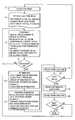
- FIGUREis a flow chart of a tool flow process for physical design of an integrated circuit in accordance with an embodiment of the present invention.
- an improved IC design methodologymay utilize manual placement of certain critical circuit elements followed by circuit optimization based on timing estimates at an early stage in the design process. Therefore, embodiments of the present invention are generally directed to a tool flow process for physical design of an IC, such as an ASIC, which includes manual pre-placement of certain critical circuits followed by circuit optimization based on timing estimates at an early stage in the design process.
- the pre-placement processmay involve locating and fixing strategic electrical infrastructure such as clock trees, electro-static discharge (ESD) protection circuits, input/output (IO) circuits, bitstacks, etc. followed by automatic placement of the remainder of the chip circuits.
- a starting point for estimation of parameters such as parasitics, timing, routing congestion and circuit areais thus established which improves the accuracy and stability of the estimated parameters. Consequently, this speeds up the design iterative loop and design phase, maximizes die usage and frequency, and improves the predictability of the results.
- Design synthesis step 2is preferably performed using DESIGN COMPILERTM which is a circuit design synthesis software tool which may be purchased from Synopsys, Inc. of Mountain View, Calif., or other suitable circuit design synthesis tool.
- Synthesizing an ASIC designis an iterative process which begins with defining the timing constraints for each block of the design. The timing constraints define the relationship of each signal relative to the clock input for a particular block.
- a file defining the synthesis environmentis also typically utilized.
- the synthesis environment filespecifies the cell libraries and other relevant information used by the circuit design synthesis tool during synthesis.
- the command line interface of the Synopsys synthesis tool mentioned abovemay be invoked, for example, by either typing dc_shell or dc_shell-t in a UNIX® shell.
- the dc_shell commandis based on Synopsys's own language, while the dc_shell-t command is based on the standard Tcl language.
- the circuit design synthesis toolmay then read the register transfer level (RTL) code of the design using the timing constraints and synthesizes the code to a structural level, i.e. generating a mapped gate-level netlist.
- RTLregister transfer level
- the generated gate-level netlistmay be run through a DFT (Design-For-Test) and clock tree build step 4 utilizing an IBMTM software BOOLEDOZERTM tool, which is part of the IBM BLUE LOGIC® software design methodology flow tool suite used industry-wide and available commercially from the IBM Corporation of Waltham, Mass., or other logic synthesis tool.
- clock tree build of the illustrated embodimentinvolves inserting the clock tree buffers (step 4 of the FIGURE).
- DFT techniquesare increasingly becoming popular among ASIC designers as merging testability early in the design cycle generally leads to reduced debugging time normally spent at the tester after the ASIC has been fabricated.
- Two of the main DFT techniques currently used by ASIC-designersinclude scan insertion, and boundary scan insertion.
- Boundary scanis normally used to test the board connections without unplugging the chip from the board.
- Scanis a well-known technique used by chip designers to test the chip for defects such as, for example, stuck-at faults.
- Scan insertionentails replacing all the flip-flops in the design with special flops containing built-in logic for testability purposes.
- a well-known architectureentails the use of a multiplexed flip-flop which basically involves the incorporation of a 2-input MUX at the input of a D-type flip-flop.
- the select line of the MUXdefines the operational mode of the device, i.e. whether the MUX is in a normal operational mode (normal data coming in) or in a test mode (scanned data coming in).
- the scan-flopsare linked together using the scan-data input of the MUX to form a scan chain which functions like a serial shift register.
- IBM's method of LSSD-level sensitive scan designwhich utilizes a master and slave latch, and multiple clocks.
- the logic synthesis toolmay be used to connect the scan chains, insert testability circuits such as MUXs and boundary scan circuits, and run scripts to add other structures to the netlist such as decoupling capacitors for the top level logic hierarchy.
- Synopsys®adds DFT capabilities to the DESIGN COMPILERTM suite of tools through its DFT Compiler (DFTC) which may be invoked, for example, by: dc_shell-t>set_scan_configuration-style multiplexed_flip_flop *** followed by insert_scan ***.
- DFTCDFT Compiler
- the command to stitch the scan chains in Physical CompilerTMmay be invoked, for example, by: ***insert_dft***.
- a scriptmay be generated using CHIPBENCHTM (a front end software floor-planning tool from the IBMTM BLUE LOGICTM design flow tool suite), or other suitable design tool, commands which would select by name and characteristic various critical electrical infrastructure from the (DFT and clock tree built) netlist and interact with the designer to manually pre-place (fix) the same in a specific order in respective pre-set areas on the die at a relatively early stage in the design process to ensure repeatability, step 6 of the FIGURE.
- Such a scriptmay call a plurality of sub-scripts in a pre-determined order to allow the designer to locate and manually pre-place certain critical electrical infrastructure on the die early in the physical design process.
- the various sub-scriptsmay be programmed to run as follows:
- Sub-script 1Locate and pre-place (fix) IO (input/output) circuitry to ensure that IO macros (cell library elements containing groups of IO circuits) are close to their respective C 4 bumpouts (input/output ports on the die);
- Sub-script 2Locate and pre-place (fix) electro-static discharge (ESD) protection circuits which are to be disposed within a certain distance of the IO macros;
- Sub-script 3Locate and pre-place (fix) large register arrays/files, i.e. large macro files that function as arrays of flip-flops so that they are more compact than discrete flip-flops;
- Sub-script 4Locate and pre-place (fix) clock tree buffers as optimally as possible in the remaining die area in an H-tree format
- Sub-script 5Locate and pre-place (fix) bitstack (standard cell gate) structures such as high-speed link interfaces;
- Sub-script 6Locate and pre-place (fix) certain critical data paths such as synchronizers and repeaters, and circuits that need certain balancing for their routes to match resistances, loads or delays for electrical needs;
- Sub-script 7Locate and pre-place (fix) de-coupling capacitors that have to be disposed in large stacks and in small numbers at regular intervals around the chip;
- Sub-script 8(prefill step). Insert N-well taps at regular intervals around the chip (die);
- Sub-script 9Locate and pre-place (fix) boundary scan circuits which are placed next to the IO circuits such as MUXs and flip-flops used for scan paths;
- Sub-script 10Locate and pre-place (fix) de-coupling capacitors that have to be disposed close to the IO macros and around the clock tree buffers. The remainder of the de-coupling capacitors may be constrained to region bounds and placed using the ‘cplace’ command in CHIPBENCHTM, for example; and
- Sub-script 11Snap desired gates closer to other gates, if needed. Some examples may include pulling metastability flip-flops close together, or putting a buffer close to a register file output pin if the pin has a weak drive capability such as to avoid electromigration type problems, etc.
- the ASIC designermay also use the design tool, e.g., CHIPBENCHTM, to constrain all unfixed logical gates to pre-defined regions on the die using their hierarchical prefixes in accordance with standard practice, step 6 of the FIGURE.
- Region constraintsare perimeters defining which cell blocks should be placed together and in what location on the die.
- the ASIC designermay utilize the gate placement command ‘cplace’ in CHIPBENCHTM, or similar functionality of another design tool, to automatically place all unfixed logical gates into the pre-defined regions in accordance with standard practice, step 6 of the FIGURE.
- These regionsmay be pre-defined by means of a script which dictates which prefixes in the gate names go into which region.
- the ‘cplace’ algorithmdefines where all the gates would go in the regions using their connectivity information. A person skilled in the art would recognize that this placement run may also be done using timing constraints, which would make ‘cplace’ run in a timing-based mode.
- step 8 of the FIGUREplacement of the cells is checked for circuit congestion, step 8 of the FIGURE.
- the ASIC designermay use CHIPBENCHTM to check the placed cells for circuit congestion.
- CHIPBENCHTMmay be used to estimate how easy it would be to wire all cells together. If congestion problems are encountered, the designer may modify the early manual pre-placements, change the region constraints, or return to design synthesis (step 2 , of the FIGURE). After all congestion problems are fixed, or if no congestion problems are encountered, the placed netlist, preferably, goes through an optimization step, step 10 of the FIGURE.
- CHIPBENCHTMmay be used to perform standard scan connection optimization of the placed netlist.
- the scan connection optimization stepmay be desirable since BOOLEDOZERTM is designed to connect the scan chains using an alphabetical naming convention which, after the placement run, may result in the flip-flops (that are scan connected to each other) being disposed not physically close to each other.
- One of the reasons scan connections are made by BOOLEDOZERTM according to one embodimentis that the tool models the extra load on a flip-flop output early on and the chain lengths are known and balanced.
- the ‘ScanOpt’ command in CHIPBENCHTMmay be utilized to re-arrange the scan connections in a certain chain based on placement proximity.
- Other techniques and/or toolsmay be used to perform scan connection optimization after placement, such as, for example, PHYSICAL COMPILERTM from Synopsys, Inc. Scan connection optimization is followed by standard clock tree optimization of the placed netlist according to the illustrated embodiment.
- CHIPBENCHTMmay be utilized to perform circuit optimization of the placed netlist based on timing estimates at a relatively early stage in the design process, step 10 of the FIGURE.
- a person skilled in the artwould readily recognize that performing early circuit optimization of the placed netlist provides a good starting point for estimation of parasitics, timing, routing, congestion and circuit area which improves the accuracy and stability of these parameters.
- the ‘TDCopt’ command in CHIPBENCHTMmay be used to resize gates, clone gates, re-power nets to meet timing estimates, and the like.
- the designermay use the ‘ClockOpt’ command in CHIPBENCHTM to perform clock tree re-optimization of the placed netlist which is essentially a fine-tuning step.
- Clock tree re-optimizationis generally desired, since after the ‘TDCopt’ step (described hereinabove) some of the flip-flops may have changed size. The size changes may affect the loads on the clock tree buffers as the input capacitance of the flip-flops has changed. As a result, the clock tree may not be as skew balanced as it was before. Specifically, the clock tree that was built previously will now have different clock pin sinks, i.e.
- the ‘ClockOpt’ algorithmis programmed to decide what the new buffer sizes and new clock tree structure should look like and optimally place the buffers on the die.
- Step 12 of the FIGUREdeals generally with generating estimated routes and parasitics for the placed netlist, and, more specifically, with merging available parasitics (resistance and capacitance values) from (1) automatically generated global route (Steiner) parasitic estimates for signals, (2) parasitic results from earlier real route experiments, and (3) clock overrides or clock tool generated parasitics, in accordance with an embodiment of the present invention.
- Step 12 of the FIGUREdeals generally with generating estimated routes and parasitics for the placed netlist, and, more specifically, with merging available parasitics (resistance and capacitance values) from (1) automatically generated global route (Steiner) parasitic estimates for signals, (2) parasitic results from earlier real route experiments, and (3) clock overrides or clock tool generated parasitics, in accordance with an embodiment of the present invention.
- Global route parasiticsmay be generated using the ‘route_global’ command in CHIPBENCHTM which does not perform a detailed route, but instead estimates into which tiles (gcells) on the chip the routes would generally fall.
- the ‘route_global’ algorithmis programmed to decide which signals would go through which tiles. However, the algorithm does not assign these signals exactly based on which routing channel is used. The algorithm only has information on how many wires would have to cross a tile. Thus, if the number of wires that go through a tile is more than the total number of routing channels which can be accommodated, the tile would be over-congested.
- the ‘route_global’ algorithmprovides a color map of how congested the whole die is. If there are too many congested areas, the designer would make changes to the floor plan or move things around, or make the die larger until all congested areas are eliminated.
- the designermay also use the ‘clockPro’ command in BOOLEDOZERTM to obtain parasitic estimates for clocks.
- the ‘clockPro’ algorithm(clock tool) builds the initial clock tree and provides estimates of what the parasitics would be. Until real clock tree routes are performed, these parasitic estimates can be used. If no parasitic estimates or real route data is available, the chip designer may use clock overrides to make the clocks ideal, step 12 of the FIGURE.
- Step 14 of the FIGUREdeals with running standard static timing analysis on the placed netlist with global route/estimated routes which may be performed using EINSTIMERTM, also part of the IBM BLUE LOGIC® software design flow tool suite. This type of analysis times all circuits in the design to determine whether the specified clock periods are met. If certain paths fail to meet the prescribed timing requirements, the designer may go back to step 2 (design synthesis), as generally shown in block 16 of the FIGURE, or back to placement step 6 depending on the severity of the problem.
- a master scriptmay be generated using IBM BLUE LOGIC® ASIC design flow tool suite commands which would automatically call each of the above-identified tools in a predetermined order.
- Such a master scriptmay incorporate the (early manual) pre-placement script referred to hereinabove, and simplify and streamline the ASIC design tool flow process while enabling first-time-right design efficiency.
- a person skilled in the artwould readily recognize that incorporating a master script of this kind in the ASIC design tool flow process would readily translate into reduced development time and costs, allowing designers to bring their complex designs to market quickly.
- the following master script(which incorporates the various pre-placement sub-scripts described hereinabove) was generated in connection with a tool flow process for physical design of an ASIC intended generally for a PCIX-based server application: PART 1: Steps up to TDCOpt # set prefix for current run set prefix “VIM0426_pass1” set edif_tag “EDIF042601” echo [exec date] echo $auto_path # this list path that CB searches for tcl scripts echo [get_parm_path] # the constraints file gives coordinates and cell types of IOs, ESD cells, etc read_parms -command read_design -file $ ⁇ prefix ⁇ _before_init.parms report_parm -command read_design read_design -initialize -pdl_package_file ⁇ IA3D12886_A0 ⁇ -chip_image ⁇ IA3D128
- the placed netlistmay be provided to a layout vendor which will perform a real route of all the nets in the design in accordance with standard practice.
- the vendormay extract the actual parasitics (capacitance and resistance values), step 18 of the FIGURE, and provide the generated layout to the ASIC designer for timing analysis.
- the designermay then run static timing analysis on the real routes with actual parasitics, step 20 of the FIGURE, in accordance with standard practice. Specifically, the designer may feed the actual capacitance and resistance values back into the EINSTIMERTM software tool to determine whether timing requirements are met, according to one embodiment.
- the designermay have to go back to placement step 6 of the FIGURE, or to design synthesis step 2 depending on the severity of the problem. If no timing problems are encountered, or after all timing problems have been fixed (block 22 FIGURE), the tool flow process is complete.
- ECOengineering change order
- the ASIC designermay add a few gates like buffers, or change the size of gates in the CHIPBENCHTM tool to fix some timing violations, like capacitance or slew or hold violations.
- the designermay insert and place some buffers in the netlist or move some buffers around, or upsize some buffers and legalize the placement of the buffers, if needed, without additional effort.
- novel tool flow processsolves the instability problems associated with working with estimations of area and parasitics while working to get closure on timing, routing congestion and die area.
- the novel tool flow processincreases the repeatability and predictability of results while smoothing out and stabilizing the analysis being done by the chip designer.
Landscapes
- Engineering & Computer Science (AREA)
- Computer Hardware Design (AREA)
- Physics & Mathematics (AREA)
- Theoretical Computer Science (AREA)
- Evolutionary Computation (AREA)
- Geometry (AREA)
- General Engineering & Computer Science (AREA)
- General Physics & Mathematics (AREA)
- Design And Manufacture Of Integrated Circuits (AREA)
Abstract
Description
- The present disclosure relates generally to development of integrated circuits (ICs) and more particularly to a tool flow process for physical design of ICs.[0001]
- An integrated circuit (IC) typically includes thousands of transistors fabricated on a monolithic crystalline lattice usually comprised of silicon or other semiconductor material. The transistors are selectively interconnected through the use of one or more interconnect layers comprised of conductive material to achieve a particular functionality which is dictated by the application to which the integrated circuit is directed. As application specific integrated circuits (ASICs) become more complex, various computer aided design (CAD) tools are being used to more efficiently design such circuits. The time required for a full scale design is greatly reduced by drawing from a library of pre-defined cells that have been fully characterized for a given wafer process flow.[0002]
- One CAD tool commonly used in integrated circuit design is a synthesis tool. The synthesis tool receives a description of the circuit, typically in hardware description language (HDL) which functionally describes the circuit, and outputs a description (netlist) of the circuit which corresponds to the actual circuit being formed on a semiconductor wafer. A netlist is a detailed list of circuit elements which will to produce the ASIC and the interconnections among the various circuit elements.[0003]
- If the design is functionally correct and meets basic timing criteria, the netlist is passed as input to a software placement tool. Placement involves allocating each cell of the design to a physical location on the silicon chip such that the cells could subsequently be interconnected by routing software. A group of cells (cell block) which performs a certain function, and blocks of cells which are closely related electrically, are physically placed as close as possible to each other. Physical proximity conserves space on the chip, simplifies routing and enhances circuit performance. Placement is also concerned with excess capacitance and resistance values caused by long interconnect paths between cells which may cause signal delays and lead to functional failures. Another goal of placement is to allocate the cells such that interconnections between cells are minimized and undue routing congestion is avoided. Placement may be done manually and/or automatically. If placement is done manually, the designer directs the software placement tool to a particular location on the chip (die) where a cell or a block of cells is to be placed. Automatic placement uses sophisticated algorithms and a pre-defined cell library to allocate the cells to various locations on the chip. Each cell in the library contains a variety of attributes describing the function, timing and other information related to each cell.[0004]
- After placement is complete, a software router tool is used to generate an interconnected layout of the ASIC. The purpose of routing is to connect points in each net of the logic design so that the connections required between cells are complete. The router tool performs the interconnections to ensure most efficient area utilization. The router tool also takes into account timing considerations for worst case delay paths. Actual parasitic capacitances and resistances are fed into an analyzer which provides an accurate assessment of circuit performance under various process and temperature conditions. If any routing problems become evident, appropriate design changes are made. If no routing problems become evident, masks for fabricating the circuit may be generated.[0005]
- In general, routing problems can be significantly reduced if the cells have been optimally placed during the placement stage. Incorrect placement of cells may lead to layout failure which in some cases only becomes apparent at the end, i.e. when the final few connections are being added. Hence, it is critical that optimal placement of the cells is achieved during the placement stage. However, some standard placement-based synthesis tools do not work well on large-size ASIC chip designs. In other CAD tools, optimization is done relatively late in the design cycle which may result in re-synthesis or too many iterations due to discrepancy between parasitics from different sources. Also, existing non-placement based synthesis tools do not produce circuits which successfully close in timing and area since such tools typically use wireload model estimates.[0006]
- An embodiment of the present invention is directed to a circuit design flow process comprising using a mapped gate-level netlist to pre-place critical electrical infrastructure on an integrated circuit (IC) die to ensure repeatability, and placing the remaining electrical infrastructure on the IC die.[0007]
- Another embodiment of the present invention provides a circuit design flow process comprising, generating a mapped gate-level netlist, and using the gate-level netlist to pre-place critical electrical infrastructure on an integrated circuit (IC) die to ensure repeatability.[0008]
- An embodiment of the present invention provides a circuit design flow process comprising, generating a mapped gate-level netlist, running the gate-level netlist through a design-for-test (DFT) and clock tree build stage, and using the resultant netlist to pre-place critical electrical infrastructure on an integrated circuit (IC) die to ensure repeatability.[0009]
- Another embodiment of the present invention provides a tool flow process for physical design of an integrated circuit (IC), comprising, using a design synthesis tool to generate a mapped gate-level netlist, using a master script to call a first tool to perform a design-for-test (DFT) and clock tree build of the gate-level netlist, the resultant netlist containing critical electrical infrastructure for utilization in the IC physical design, using the master script to call a second tool to perform pre-placement of the critical electrical infrastructure on an IC die to ensure repeatability, using the master script to call the second tool to perform placement of the remaining electrical infrastructure on the IC die, the placements constituting a placed netlist, and using the master script to call the second tool to perform circuit optimization of the placed netlist based on timing estimates.[0010]
- The FIGURE is a flow chart of a tool flow process for physical design of an integrated circuit in accordance with an embodiment of the present invention.[0011]
- Hereinafter, some preferred embodiments of the present invention will be described in detail with reference to the related drawings of the FIGURE. Additional embodiments, features and/or advantages of the invention will become apparent from the ensuing description or may be learned by practicing the invention.[0012]
- The following description includes the best mode presently contemplated for carrying out the invention. This description is not to be taken in a limiting sense, but is made merely for the purpose of describing the general principles of the invention.[0013]
- In developing the present invention, it has been discovered that an improved IC design methodology may utilize manual placement of certain critical circuit elements followed by circuit optimization based on timing estimates at an early stage in the design process. Therefore, embodiments of the present invention are generally directed to a tool flow process for physical design of an IC, such as an ASIC, which includes manual pre-placement of certain critical circuits followed by circuit optimization based on timing estimates at an early stage in the design process. Specifically, the pre-placement process may involve locating and fixing strategic electrical infrastructure such as clock trees, electro-static discharge (ESD) protection circuits, input/output (IO) circuits, bitstacks, etc. followed by automatic placement of the remainder of the chip circuits. A starting point for estimation of parameters such as parasitics, timing, routing congestion and circuit area is thus established which improves the accuracy and stability of the estimated parameters. Consequently, this speeds up the design iterative loop and design phase, maximizes die usage and frequency, and improves the predictability of the results.[0014]
- Turning to the FIGURE, a flow diagram of design of an integrated circuit in accordance with an embodiment of the present invention is shown. The flow chart of the embodiment illustrated in the FIGURE begins with[0015]
design synthesis step 2.Design synthesis step 2 is preferably performed using DESIGN COMPILER™ which is a circuit design synthesis software tool which may be purchased from Synopsys, Inc. of Mountain View, Calif., or other suitable circuit design synthesis tool. Synthesizing an ASIC design is an iterative process which begins with defining the timing constraints for each block of the design. The timing constraints define the relationship of each signal relative to the clock input for a particular block. A file defining the synthesis environment is also typically utilized. The synthesis environment file specifies the cell libraries and other relevant information used by the circuit design synthesis tool during synthesis. The command line interface of the Synopsys synthesis tool mentioned above may be invoked, for example, by either typing dc_shell or dc_shell-t in a UNIX® shell. The dc_shell command is based on Synopsys's own language, while the dc_shell-t command is based on the standard Tcl language. The circuit design synthesis tool may then read the register transfer level (RTL) code of the design using the timing constraints and synthesizes the code to a structural level, i.e. generating a mapped gate-level netlist. - The generated gate-level netlist may be run through a DFT (Design-For-Test) and clock[0016]
tree build step 4 utilizing an IBM™ software BOOLEDOZER™ tool, which is part of the IBM BLUE LOGIC® software design methodology flow tool suite used industry-wide and available commercially from the IBM Corporation of Waltham, Mass., or other logic synthesis tool. Specifically, clock tree build of the illustrated embodiment involves inserting the clock tree buffers (step 4 of the FIGURE). - DFT techniques are increasingly becoming popular among ASIC designers as merging testability early in the design cycle generally leads to reduced debugging time normally spent at the tester after the ASIC has been fabricated. Two of the main DFT techniques currently used by ASIC-designers include scan insertion, and boundary scan insertion. Boundary scan is normally used to test the board connections without unplugging the chip from the board. Scan is a well-known technique used by chip designers to test the chip for defects such as, for example, stuck-at faults. Scan insertion entails replacing all the flip-flops in the design with special flops containing built-in logic for testability purposes. For example, a well-known architecture entails the use of a multiplexed flip-flop which basically involves the incorporation of a 2-input MUX at the input of a D-type flip-flop. The select line of the MUX defines the operational mode of the device, i.e. whether the MUX is in a normal operational mode (normal data coming in) or in a test mode (scanned data coming in). The scan-flops are linked together using the scan-data input of the MUX to form a scan chain which functions like a serial shift register. Another example is IBM's method of LSSD-level sensitive scan design which utilizes a master and slave latch, and multiple clocks.[0017]
- After the clock tree buffers have been inserted, the logic synthesis tool may be used to connect the scan chains, insert testability circuits such as MUXs and boundary scan circuits, and run scripts to add other structures to the netlist such as decoupling capacitors for the top level logic hierarchy.[0018]
- A person skilled in the art would recognize that other software tools/techniques may be utilized to incorporate early testability features in the ASIC design as long as such other tools/techniques do not depart from the intended purpose of the present invention. For example, Synopsys® adds DFT capabilities to the DESIGN COMPILER™ suite of tools through its DFT Compiler (DFTC) which may be invoked, for example, by: dc_shell-t>set_scan_configuration-style multiplexed_flip_flop *** followed by insert_scan ***. The command to stitch the scan chains in Physical Compiler™ may be invoked, for example, by: ***insert_dft***.[0019]
- In accordance with a preferred embodiment of the present invention, a script may be generated using CHIPBENCH™ (a front end software floor-planning tool from the IBM™ BLUE LOGIC™ design flow tool suite), or other suitable design tool, commands which would select by name and characteristic various critical electrical infrastructure from the (DFT and clock tree built) netlist and interact with the designer to manually pre-place (fix) the same in a specific order in respective pre-set areas on the die at a relatively early stage in the design process to ensure repeatability,[0020]
step 6 of the FIGURE. Such a script may call a plurality of sub-scripts in a pre-determined order to allow the designer to locate and manually pre-place certain critical electrical infrastructure on the die early in the physical design process. For example, the various sub-scripts may be programmed to run as follows: - Sub-script 1. Locate and pre-place (fix) IO (input/output) circuitry to ensure that IO macros (cell library elements containing groups of IO circuits) are close to their respective C[0021]4 bumpouts (input/output ports on the die);
- Sub-script 2. Locate and pre-place (fix) electro-static discharge (ESD) protection circuits which are to be disposed within a certain distance of the IO macros;[0022]
- Sub-script 3. Locate and pre-place (fix) large register arrays/files, i.e. large macro files that function as arrays of flip-flops so that they are more compact than discrete flip-flops;[0023]
- Sub-script 4. Locate and pre-place (fix) clock tree buffers as optimally as possible in the remaining die area in an H-tree format;[0024]
- Sub-script 5. Locate and pre-place (fix) bitstack (standard cell gate) structures such as high-speed link interfaces;[0025]
- Sub-script 6. Locate and pre-place (fix) certain critical data paths such as synchronizers and repeaters, and circuits that need certain balancing for their routes to match resistances, loads or delays for electrical needs;[0026]
- Sub-script 7. Locate and pre-place (fix) de-coupling capacitors that have to be disposed in large stacks and in small numbers at regular intervals around the chip;[0027]
- Sub-script 8 (prefill step). Insert N-well taps at regular intervals around the chip (die);[0028]
- Sub-script 9. Locate and pre-place (fix) boundary scan circuits which are placed next to the IO circuits such as MUXs and flip-flops used for scan paths;[0029]
- Sub-script 10. Locate and pre-place (fix) de-coupling capacitors that have to be disposed close to the IO macros and around the clock tree buffers. The remainder of the de-coupling capacitors may be constrained to region bounds and placed using the ‘cplace’ command in CHIPBENCH™, for example; and[0030]
- Sub-script 11. Snap desired gates closer to other gates, if needed. Some examples may include pulling metastability flip-flops close together, or putting a buffer close to a register file output pin if the pin has a weak drive capability such as to avoid electromigration type problems, etc.[0031]
- Having fixed the critical electrical infrastructure early in the design process, the ASIC designer may also use the design tool, e.g., CHIPBENCH™, to constrain all unfixed logical gates to pre-defined regions on the die using their hierarchical prefixes in accordance with standard practice,[0032]
step 6 of the FIGURE. Region constraints are perimeters defining which cell blocks should be placed together and in what location on the die. - Thereafter, the ASIC designer may utilize the gate placement command ‘cplace’ in CHIPBENCH™, or similar functionality of another design tool, to automatically place all unfixed logical gates into the pre-defined regions in accordance with standard practice,[0033]
step 6 of the FIGURE. These regions may be pre-defined by means of a script which dictates which prefixes in the gate names go into which region. The ‘cplace’ algorithm defines where all the gates would go in the regions using their connectivity information. A person skilled in the art would recognize that this placement run may also be done using timing constraints, which would make ‘cplace’ run in a timing-based mode. - Upon completion of[0034]
step 6, placement of the cells is checked for circuit congestion,step 8 of the FIGURE. For example, the ASIC designer may use CHIPBENCH™ to check the placed cells for circuit congestion. Specifically, CHIPBENCH™ may be used to estimate how easy it would be to wire all cells together. If congestion problems are encountered, the designer may modify the early manual pre-placements, change the region constraints, or return to design synthesis (step 2, of the FIGURE). After all congestion problems are fixed, or if no congestion problems are encountered, the placed netlist, preferably, goes through an optimization step, step10 of the FIGURE. - For example, CHIPBENCH™ may be used to perform standard scan connection optimization of the placed netlist. The scan connection optimization step may be desirable since BOOLEDOZER™ is designed to connect the scan chains using an alphabetical naming convention which, after the placement run, may result in the flip-flops (that are scan connected to each other) being disposed not physically close to each other. One of the reasons scan connections are made by BOOLEDOZER™ according to one embodiment is that the tool models the extra load on a flip-flop output early on and the chain lengths are known and balanced. The ‘ScanOpt’ command in CHIPBENCH™ may be utilized to re-arrange the scan connections in a certain chain based on placement proximity. Other techniques and/or tools may be used to perform scan connection optimization after placement, such as, for example, PHYSICAL COMPILER™ from Synopsys, Inc. Scan connection optimization is followed by standard clock tree optimization of the placed netlist according to the illustrated embodiment.[0035]
- In accordance with another embodiment of the present invention, CHIPBENCH™ may be utilized to perform circuit optimization of the placed netlist based on timing estimates at a relatively early stage in the design process, step[0036]10 of the FIGURE. A person skilled in the art would readily recognize that performing early circuit optimization of the placed netlist provides a good starting point for estimation of parasitics, timing, routing, congestion and circuit area which improves the accuracy and stability of these parameters. Specifically, the ‘TDCopt’ command in CHIPBENCH™ may be used to resize gates, clone gates, re-power nets to meet timing estimates, and the like.
- In accordance with yet another embodiment of the present invention, the designer may use the ‘ClockOpt’ command in CHIPBENCH™ to perform clock tree re-optimization of the placed netlist which is essentially a fine-tuning step. Clock tree re-optimization is generally desired, since after the ‘TDCopt’ step (described hereinabove) some of the flip-flops may have changed size. The size changes may affect the loads on the clock tree buffers as the input capacitance of the flip-flops has changed. As a result, the clock tree may not be as skew balanced as it was before. Specifically, the clock tree that was built previously will now have different clock pin sinks, i.e. there could be worse clock skew relative to the previous clock tree. Hence, fine-tuning the clock tree leaves at this stage would help keep the clock skew down and prevent problems downstream in meeting timing requirements. Some of the critical clocks may be re-built to account for the new flip-flop sizes. Furthermore, the reset clock tree and the test clocks related to these flip-flops may be optimized as well, but not as stringently, since their timing requirements are much more relaxed. Specifically, the ‘ClockOpt’ algorithm is programmed to decide what the new buffer sizes and new clock tree structure should look like and optimally place the buffers on the die.[0037]
- [0038]
Step 12 of the FIGURE deals generally with generating estimated routes and parasitics for the placed netlist, and, more specifically, with merging available parasitics (resistance and capacitance values) from (1) automatically generated global route (Steiner) parasitic estimates for signals, (2) parasitic results from earlier real route experiments, and (3) clock overrides or clock tool generated parasitics, in accordance with an embodiment of the present invention. - Global route parasitics may be generated using the ‘route_global’ command in CHIPBENCH™ which does not perform a detailed route, but instead estimates into which tiles (gcells) on the chip the routes would generally fall. The ‘route_global’ algorithm is programmed to decide which signals would go through which tiles. However, the algorithm does not assign these signals exactly based on which routing channel is used. The algorithm only has information on how many wires would have to cross a tile. Thus, if the number of wires that go through a tile is more than the total number of routing channels which can be accommodated, the tile would be over-congested. Specifically, the ‘route_global’ algorithm provides a color map of how congested the whole die is. If there are too many congested areas, the designer would make changes to the floor plan or move things around, or make the die larger until all congested areas are eliminated.[0039]
- Whenever parasitic data from previous real route experiments is available and the placement of some of some previously fixed gates such as clock buffers and bitstacks, has not changed, the designer can use the earlier experimental parasitic values instead of global route parasitic (Steiner) estimates. As a general rule, as soon as the designer is certain that these gates are not going to move on the die and the two end points are fixed in location—for example, from C[0040]4 to the IO or from the IO to bitstack—then, the designer can route the signals between fixed gates once and use real parasitics from that point on instead of global route parasitics to shorten the overall design cycle.
- The designer may also use the ‘clockPro’ command in BOOLEDOZER™ to obtain parasitic estimates for clocks. The ‘clockPro’ algorithm (clock tool) builds the initial clock tree and provides estimates of what the parasitics would be. Until real clock tree routes are performed, these parasitic estimates can be used. If no parasitic estimates or real route data is available, the chip designer may use clock overrides to make the clocks ideal, step[0041]12 of the FIGURE.
- [0042]
Step 14 of the FIGURE deals with running standard static timing analysis on the placed netlist with global route/estimated routes which may be performed using EINSTIMER™, also part of the IBM BLUE LOGIC® software design flow tool suite. This type of analysis times all circuits in the design to determine whether the specified clock periods are met. If certain paths fail to meet the prescribed timing requirements, the designer may go back to step2 (design synthesis), as generally shown inblock 16 of the FIGURE, or back toplacement step 6 depending on the severity of the problem. - In accordance with yet another embodiment of the present invention, a master script may be generated using IBM BLUE LOGIC® ASIC design flow tool suite commands which would automatically call each of the above-identified tools in a predetermined order. Such a master script may incorporate the (early manual) pre-placement script referred to hereinabove, and simplify and streamline the ASIC design tool flow process while enabling first-time-right design efficiency. A person skilled in the art would readily recognize that incorporating a master script of this kind in the ASIC design tool flow process would readily translate into reduced development time and costs, allowing designers to bring their complex designs to market quickly.[0043]
- In accordance with one exemplary embodiment of the present invention, the following master script (which incorporates the various pre-placement sub-scripts described hereinabove) was generated in connection with a tool flow process for physical design of an ASIC intended generally for a PCIX-based server application:[0044]
PART 1: Steps up to TDCOpt # set prefix for current run set prefix “VIM0426_pass1” set edif_tag “EDIF042601” echo [exec date] echo $auto_path # this list path that CB searches for tcl scripts echo [get_parm_path] # the constraints file gives coordinates and cell types of IOs, ESD cells, etc read_parms -command read_design -file ${prefix}_before_init.parms report_parm -command read_design read_design -initialize -pdl_package_file {IA3D12886_A0} -chip_image {IA3D12886} nitialize_power -design_object_type {chip} -constraints_file {HDP_PDL.FP11} # Write out initialized chip exec mkdir -p ${prefix}_after_init write_design -directory ${prefix}_after_init -name {top} -no_children write_parms -command read_design -file ${prefix}_after_init.parms current_cell -root check_placement -overlap # Scan trace trace_scan_path -hierarchy_levels 99 -output_directory {HDP/reports} -chain_types {all} # Save as_after_scanTrace exec mkdir -p VIM/${prefix}_after_scanTrace write_design -directory VIM/${prefix}_after_scanTrace -name {top} -no_children write_parms -command read_design -file etc/app-parms/${prefix}_after_scanTrace.parms # Trace clock nets source tcl/clock_trace.tcl # save as_clockTrace exec mkdir -p VIM/${prefix}_after_clockTrace write_design -directory VIM/${prefix}_after_clockTrace -name {top} -no_children write_parms -command read_design -file etc/app- parms/${prefix}_after_clockTrace.parms # make blocks source tcl/create_hier.tcl # Now estimate block size source tcl/place_size_rlms_core.tcl echo [cputime] # place and size of rlms (blocks) current_cell -root echo “############ Placing and sizing blocks ##############” source tcl/move_and_size_rlms.tcl current_cell -root # save as_hier FORCE SAVE exec mkdir -p VIM/${prefix}_HIER_PLACED write_design -all -directory VIM/${prefix}_HIER_PLACED -name {top} write_parms -command read_design -file etc/app-parms/${prefix}_HIER_PLACED.parms # flatten and create movebounds # Generated by generate_placeSizeRlmsCore_createMb.pl # After this step, the Register Arrays are back on the top level, in the lower left hand of the chip # Need to click on Cell GROUP movebounds to see them echo “############ Creating movebounds ###########” source tcl/create_mb.tcl echo “############ Removing ioaffinity gates from movebounds ###########” source tcl/remove_from_mbound.tcl echo “############ Adding decaps to movebounds ###########” source tcl/add_decaps_to_mbounds.tcl echo “############ Setting last_unused for place_old_decap.tcl end point to: $last_unused” echo “ Set in add_decaps_to_mbounds.tcl script” current_cell -root # Save as_mbounds exec mkdir -p VIM/${prefix}_mbounds write_design VIM/${prefix}_mbounds -name {top} -no_children write_parms -command read_design -file etc/app-parms/${prefix}_mbounds.parms echo [cputime] # place clock buffers (SCB), register files (RA), bitstacks and balanced route gates echo “############ Placing RAs ##############” source tcl/place_ra.tcl echo “############ Placing SCBs #############” source tcl/place_scb.tcl echo “############ Placing bitstacks ############” source tcl/place_bstack.tcl echo “############ Sourcing new bstacks... ############” current_cell -root source tcl/place_io_bstack.tcl echo “############ Placing balanced route related gates #####” current_cell -root source tcl/balanced_route_placement.tcl echo [cputime] current_cell -root check_placement -overlap # Save as_fixed exec mkdir -p VIM/${prefix}_fixed write_design -directory VIM/${prefix}_fixed -name {top} -no_children write_parms -command read_design -file etc/app-parms/${prefix}_fixed.parms # more decaps echo “############ Placing NEW DECAPS ###############” source tcl/place_new_decaps.tcl echo [cputime] current_cell -root check_placement -overlap # save as_large_decaps exec mkdir -p VIM/${prefix}_large_decaps write_design -directory VIM/${prefix}_large_decaps -name {top} -no_children write_parms -command read_design -file etc/app-parms/${prefix}_large_decaps.parms #prefill (nwell contacts) echo “############ PREFILL ############” current_cell -root add_filler_cells -prefill echo [cputime] current_cell -root check_placement -overlap # save as_prefill exec mkdir -p VIM/${prefix}_prefill write_design -directory VIM/${prefix}_prefill -name {top} -no_children write_parms -command read_design -file etc/app-parms/${prefix}_prefill.parms # place wrappers echo “############ Placing RA wrappers ##########” source tcl/place_ra_wrappers.tcl echo [cputime] current_cell -root check_placement -overlap #Save as_wrappers exec mkdir -p VIM/${prefix}_wrappers write_design -directory VIM/${prefix}_wrappers -name {top} -no_children write_parms -command read_design -file etc/app-parms/${prefix}_wrappers.parms # ioaffinity placement echo “############ Placing ioaffinity #############” source tcl/io_affinity.fixwarn.tcl io_affinity ioaffinity/io_affinity_pd.$edif_tag echo [cputime] current_cell -root check_placement -overlap # save as_affinitized exec mkdir -p VIM/${prefix}_affinitized write_design VIM/${prefix}_affinitized -name {top} -no_children write_parms -command read_design -file etc/app-parms/${prefix}_affinitized.parms # decaps around IO and SCBs # NOTE: Place only 1 ring around!! echo “############ Placing DECAPS ###############” source tcl/place_decaps_if_space_2X_new.tcl echo “############# Setting last_decap_from2X to $last_decap_from2X before calling place_old_decaps_new.tcl ” source tcl/place_old_decaps_new.tcl # save as _decaps exec mkdir -p VIM/${prefix}_decaps write_design -force_specified_only -directory VIM/${prefix}_decaps -name {top} write_parms -command read_design -file etc/app-parms/${prefix}_decaps.parms echo [cputime] current_cell -root check_placement -overlap # cplace with absolute movebounds! echo “########### Starting cplace...... ############” source tcl/cplace.tcl echo [cputime] check_placement -overlap -check_unplaced ### global route #echo “########### Starting congestion analysis.... ############” #source tcl/global_route.tcl # save as _PLACED --- FORCE SAVE! exec mkdir -p VIM/${prefix}_PLACED write_design -force_specified_only -directory VIM/${prefix}_PLACED -name {top} write_parms -command read_design -file etc/app-parms/${prefix}_placed.parms # snap moves source tcl/snap_move.tcl echo [cputime] check_placement -overlap # save as_snap_moved exec mkdir -p VIM/${prefix}_snap_moved write_design -directory VIM/${prefix}_snap_moved -name {top} -no_children write_parms -command read_design -file etc/app-parms/${prefix}_snap_moved.parms # ScanOpt optimize_scan_path -hierarchy_levels 99 -output_directory {HDP/reports} -chain_types {all} # save as _scanOpted exec mkdir -p VIM/${prefix}_scanOpted write_design -directory VIM/${prefix}_scanOpted -name {top} -no_children write_parms -command read_design -file etc/app-parms/${prefix}_scanOpted.parms current_cell -root check_placement -overlap # ClockOpt source tcl/clock_opt.tcl # save as _clockOpted exec mkdir -p VIM/${prefix}_clockOpted write_design -directory VIM/${prefix}_clockOpted -name {top} -no_children write_parms -command read_design -file etc/app-parms/${prefix}_clockOpted.parms current_cell -root check_placement -check_unplaced # Legalize source tcl/legalize.tcl echo [cputime] current_cell -root check_placement -overlap -check_unplaced echo “### FIXING all global clock cells in place!” current_cell -root select_cell -name “glob_clk_box_0_*” set_location_fixed -value 1 current_cell -root # Save as _legalized exec mkdir -p VIM/${prefix}_LEGALIZED write_design -force_specified_only -directory VIM/${prefix}_LEGALIZED -name {top} write_parms -command read_design -file /etc/app-parms/${prefix}_LEGALIZED.parms set_ignore_pin -scan FALSE -clock FALSE PART 2: RUN TDCopt at this point #### NEED TO GENERATE NEW clock optimization FILES FROM TDCOPTED VIM. PART 3: Steps after TDCopt # set prefix for current run set prefix “VIM0426_pass1” set edif_tag “EDIF0426” echo [exec date] echo $auto_path # this list path that CB searches for tcl scripts echo [get_parm_path] # load _TDCOPT vim # call legalize_after_tdcopt.tcl # look at placement errors in member group window. Choose groups of fixed gates if necessary , # give list a name: set unfixed_splitters [list_selection] and unfix. # Call legalize_after_tdcopt again. # Fix the list of gates! set_location_fixed unfixed_splitters -value 1 # repeat as necessary # Save VIM and parms so that you can load them for this tcl script. # Therefore, save parms as: ${prefix}_tdcopt_LEGALIZED.parms as used below. # read_tdcopt_LEGALIZED parms read parms -command read design -file etc/app-parms/${prefix}_tdcopt_LEGALIZED.parms report_parm -command read_design read_design -name {top} current_cell -root check_placement -overlap -check_unplaced # clockOpt source tcl/clock_opt_glob_clk.tcl echo [cputime] # save as reOpted exec mkdir -p VIM/${prefix}_reOpted write_design -directory VIM/${prefix}_reOpted -name {top} -no_children write_parms -command read_design -file etc/app-parms/${prefix}_reOpted.parms # Legalize source tcl/legalize_after_reOpt.tcl # Save as _legalized exec mkdir -p VIM/${prefix}_reOpted_LEGALIZED write_design -force_specified_only -directory VIM/${prefix}_reOpted_LEGALIZED -name {top} write_parms -command read_design -file etc/app- parms/${prefix}_reOpted_LEGALIZED.parms current_cell -root set_ignore_pin -scan FALSE -clock FALSE set_ignore_pin -clock FALSE source tcl/global_route.tcl ### rap/rc generation source tcl/generate_cap_rc.tcl echo [cputime] - After completion of[0045]
step 14, the placed netlist may be provided to a layout vendor which will perform a real route of all the nets in the design in accordance with standard practice. Once all the nets are connected in the specified metal layers, the vendor may extract the actual parasitics (capacitance and resistance values), step18 of the FIGURE, and provide the generated layout to the ASIC designer for timing analysis. The designer may then run static timing analysis on the real routes with actual parasitics, step20 of the FIGURE, in accordance with standard practice. Specifically, the designer may feed the actual capacitance and resistance values back into the EINSTIMER™ software tool to determine whether timing requirements are met, according to one embodiment. If some paths fail to meet the timing requirements (block22 of the FIGURE), the designer may have to go back toplacement step 6 of the FIGURE, or to designsynthesis step 2 depending on the severity of the problem. If no timing problems are encountered, or after all timing problems have been fixed (block22 FIGURE), the tool flow process is complete. - A person skilled in the art would readily recognize that engineering change order (ECO)-type changes may be made if the timing results of[0046]
step 20 contain errors which are relatively small. For example, the ASIC designer may add a few gates like buffers, or change the size of gates in the CHIPBENCH™ tool to fix some timing violations, like capacitance or slew or hold violations. To close timing later on, the designer may insert and place some buffers in the netlist or move some buffers around, or upsize some buffers and legalize the placement of the buffers, if needed, without additional effort. - The above-described novel tool flow process solves the instability problems associated with working with estimations of area and parasitics while working to get closure on timing, routing congestion and die area. The novel tool flow process increases the repeatability and predictability of results while smoothing out and stabilizing the analysis being done by the chip designer.[0047]
- A person skilled in the art should appreciate that various other IC design methodology tools and/or configurations may be utilized in the above-described embodiments, provided that such other IC design methodology tools and/or configurations do not depart from the intended purpose and scope of the present invention.[0048]
- While the present invention has been described in detail with regards to the preferred embodiments, it should also be appreciated that various modifications and variations may be made without departing from the scope or spirit of the invention. For example, the design synthesis and placement steps may be combined in a physically aware synthesis flow such as the one utilized by PHYSICAL COMPILER™ by Synopsys, Inc.[0049]
- It is important to note that practicing the invention is not limited to the applications described hereinabove. Many other applications and/or alterations may be utilized provided that such other applications and/or alterations do not depart from the intended purpose of the present invention.[0050]
- It should further be appreciated by a person skilled in the art that features illustrated or described as part of one embodiment can be used in another embodiment to provide yet another embodiment such that the features are not limited to the specific embodiments described above. Thus, it is intended that the present invention cover all such modifications, embodiments and variations as long as such modifications, embodiments and variations come within the scope of the appended claims and their equivalents.[0051]
Claims (25)
1. A circuit design flow process comprising:
using a mapped gate-level netlist to pre-place critical electrical infrastructure on an integrated circuit (IC) die to ensure repeatability; and
placing the remaining electrical infrastructure on the IC die.
2. The circuit design flow process ofclaim 1 , further comprising:
performing circuit optimization of the placed netlist based on timing estimates.
3. The circuit design flow process ofclaim 2 , further comprising:
generating estimated routes and parasitics for the placed netlist; and
merging said estimated parasitics with other available parasitics from a plurality of sources.
4. The circuit design flow process ofclaim 3 , further comprising:
running timing analysis on the placed netlist with said estimated routes and parasitics.
5. The circuit design flow process ofclaim 4 , further comprising:
generating real routes for the nets from the placed netlist; and
extracting actual parasitics for the routed nets to generate an IC layout.
6. The circuit design flow process ofclaim 5 , further comprising:
running timing analysis on the IC layout.
7. The circuit design flow process ofclaim 1 , wherein the critical electrical infrastructure comprises at least one IO (input/output) circuit, at least one electro-static discharge (ESD) protection circuit, and at least one large register array/file.
8. The circuit design flow process ofclaim 7 , wherein the critical electrical infrastructure further comprises at least one clock tree buffer, at least one bitstack (standard cell gate) structure, and at least one critical data path.
9. The circuit design flow process ofclaim 8 , wherein the critical electrical infrastructure further comprises at least one de-coupling capacitor, and at least one boundary scan circuit.
10. The circuit design flow process ofclaim 1 , wherein the pre-placement step includes inserting N-well taps at regular intervals around the IC die.
11. A circuit design flow process comprising:
generating a mapped gate-level netlist; and
using the gate-level netlist to pre-place critical electrical infrastructure on an integrated circuit (IC) die to ensure repeatability.
12. The circuit design flow process ofclaim 11 , further comprising:
using the gate-level netlist to place the remaining electrical infrastructure on the IC die.
13. The circuit design flow process ofclaim 12 , further comprising:
performing circuit optimization of the placed netlist based on timing estimates.
14. The circuit design flow process ofclaim 13 , further comprising:
generating estimated routes and parasitics for the placed netlist; and
merging said estimated parasitics with other available parasitics from a plurality of sources.
15. The circuit design flow process ofclaim 14 , further comprising:
running timing analysis on the placed netlist with said estimated routes and parasitics.
16. The circuit design flow process ofclaim 15 , further comprising:
generating real routes for the nets from the placed netlist; and
extracting actual parasitics for the routed nets to generate an IC layout.
17. The circuit design flow process ofclaim 16 , further comprising:
running timing analysis on the IC layout.
18. A circuit design flow process comprising:
generating a mapped gate-level netlist;
running the gate-level netlist through a design-for-test (DFT) and clock tree build stage; and
using the resultant netlist to pre-place critical electrical infrastructure on an integrated circuit (IC) die to ensure repeatability.
19. The circuit design flow process ofclaim 18 , further comprising:
using the resultant gate-level netlist to place the remaining electrical infrastructure on the IC die.
20. A tool flow process for physical design of an integrated circuit (IC), comprising:
(a) using a design synthesis tool to generate a mapped gate-level netlist;
(b) using a master script to call a first tool to perform a design-for-test (DFT) and clock tree build of said gate-level netlist, the resultant netlist containing critical electrical infrastructure for utilization in the IC physical design;
(c) using said master script to call a second tool to perform pre-placement of said critical electrical infrastructure on an IC die to ensure repeatability;
(d) using said master script to call said second tool to perform placement of the remaining electrical infrastructure on the IC die, said placements constituting a placed netlist; and
(e) using said master script to call said second tool to perform circuit optimization of the placed netlist based on timing estimates.
21. The tool flow process ofclaim 20 , further comprising:
(f) using said master script to call said second tool to perform scan connection and clock tree optimization of the placed netlist; and
(g) using said master script to call said second tool to perform clock tree re-optimization of the placed netlist.
22. The tool flow process ofclaim 21 , further comprising:
(h) using said master script to call said second tool to generate estimated routes and parasitics for the placed netlist; and
(i) using said master script to call said first and second tools to merge said estimated parasitics with available parasitics from a plurality of sources.
23. The tool flow process ofclaim 22 , further comprising:
(j) using said master script to call a third tool to run timing analysis on the placed netlist with said estimated routes and parasitics.
24. The tool flow process ofclaim 23 , further comprising:
(k) generating real routes for the nets from the placed netlist; and
(l) extracting actual parasitics for the routed nets to generate an IC layout.
25. The tool flow process ofclaim 24 , further comprising the step of running timing analysis on the IC layout.
Priority Applications (2)
| Application Number | Priority Date | Filing Date | Title |
|---|---|---|---|
| US10/438,580US20040230933A1 (en) | 2003-05-15 | 2003-05-15 | Tool flow process for physical design of integrated circuits |
| JP2004134979AJP2004342100A (en) | 2003-05-15 | 2004-04-30 | Tool flow process for physical design of integrated circuit |
Applications Claiming Priority (1)
| Application Number | Priority Date | Filing Date | Title |
|---|---|---|---|
| US10/438,580US20040230933A1 (en) | 2003-05-15 | 2003-05-15 | Tool flow process for physical design of integrated circuits |
Publications (1)
| Publication Number | Publication Date |
|---|---|
| US20040230933A1true US20040230933A1 (en) | 2004-11-18 |
Family
ID=33417608
Family Applications (1)
| Application Number | Title | Priority Date | Filing Date |
|---|---|---|---|
| US10/438,580AbandonedUS20040230933A1 (en) | 2003-05-15 | 2003-05-15 | Tool flow process for physical design of integrated circuits |
Country Status (2)
| Country | Link |
|---|---|
| US (1) | US20040230933A1 (en) |
| JP (1) | JP2004342100A (en) |
Cited By (31)
| Publication number | Priority date | Publication date | Assignee | Title |
|---|---|---|---|---|
| US20040268279A1 (en)* | 2003-06-24 | 2004-12-30 | Lsi Logic Corporation | Timing constraint generator |
| US20050091627A1 (en)* | 2003-10-23 | 2005-04-28 | Lalita Satapathy | Comparison of two hierarchical netlist to generate change orders for updating an integrated circuit layout |
| US20050091621A1 (en)* | 2003-10-24 | 2005-04-28 | Goldberg David N. | Methods for designing a circuit |
| US20050120318A1 (en)* | 2003-11-28 | 2005-06-02 | Oki Electric Industry Co., Ltd. | Apparatus and method for designing semiconductor integrated circuit |
| US20050183046A1 (en)* | 2004-02-17 | 2005-08-18 | International Business Machines Corporation | Method for optimization of logic circuits for routability |
| US20050268258A1 (en)* | 2004-06-01 | 2005-12-01 | Tera Systems, Inc. | Rule-based design consultant and method for integrated circuit design |
| US20060066357A1 (en)* | 2004-09-30 | 2006-03-30 | Matsushita Electric Industrial Co., Ltd. | Semiconductor integrated circuit |
| US20060123370A1 (en)* | 2004-12-08 | 2006-06-08 | Mario Vergara-Escobar | Method for specification and integration of reusable IP constraints |
| US7152217B1 (en)* | 2004-04-20 | 2006-12-19 | Xilinx, Inc. | Alleviating timing based congestion within circuit designs |
| US20070011639A1 (en)* | 2005-07-05 | 2007-01-11 | Pitts Robert L | Placement methods for standard cell library |
| US20070079273A1 (en)* | 2005-10-05 | 2007-04-05 | Lsi Logic Corporation | Method and computer program for incremental placement and routing with nested shells |
| US7454729B1 (en)* | 2005-11-16 | 2008-11-18 | Altera Corporation | Method and system for validating testbench |
| US20100169854A1 (en)* | 2008-12-30 | 2010-07-01 | Texas Instruments Incorporated | Esd protection validator, an esd validation system and a method of validating esd protection for an ic |
| US20100192116A1 (en)* | 2009-01-23 | 2010-07-29 | International Business Machines Corporation | Minterm tracing and reporting |
| KR101006822B1 (en) | 2006-06-09 | 2011-01-10 | 오트르소테크, 엘엘씨 | Transparent test method and scan flip flop |
| US8239797B1 (en)* | 2008-09-18 | 2012-08-07 | Cadence Design Systems, Inc. | Congestion aware block placement |
| US8751996B1 (en)* | 2005-11-08 | 2014-06-10 | Pulsic Limited | Automatically routing nets according to parasitic constraint rules |
| US8887110B1 (en)* | 2007-08-22 | 2014-11-11 | Cadence Design Systems, Inc. | Methods for designing intergrated circuits with automatically synthesized clock distribution networks |
| US20140359549A1 (en)* | 2006-07-24 | 2014-12-04 | Mentor Graphics Corporation | Generating A Convergent Circuit Design From A Functional Description Using Entities Having Access To The Functional Description And To Physical Design Information |
| US10216890B2 (en) | 2004-04-21 | 2019-02-26 | Iym Technologies Llc | Integrated circuits having in-situ constraints |
| US10489549B1 (en) | 2017-12-22 | 2019-11-26 | Cadence Design Systems, Inc. | Tree-routing for specific areas of an electronic design |
| US10521097B1 (en) | 2017-09-29 | 2019-12-31 | Cadence Design Systems, Inc. | User interface to implement topology integrity throughout routing implementations |
| US10551431B1 (en)* | 2017-12-22 | 2020-02-04 | Cadence Design Systems, Inc. | EM-compliance topology in a tree router |
| US10817641B1 (en) | 2017-09-29 | 2020-10-27 | Cadence Design Systems, Inc. | Method and system to implement topology integrity throughout routing implementations |
| US10831966B1 (en) | 2019-09-11 | 2020-11-10 | International Business Machines Corporation | Multi-fanout latch placement optimization for integrated circuit (IC) design |
| US10831967B1 (en) | 2019-09-11 | 2020-11-10 | International Business Machines Corporation | Local clock buffer controller placement and connectivity |
| US10878152B1 (en) | 2019-09-11 | 2020-12-29 | International Business Machines Corporation | Single-bit latch optimization for integrated circuit (IC) design |
| US10943040B1 (en) | 2019-09-11 | 2021-03-09 | International Business Machines Corporation | Clock gating latch placement |
| US11030376B2 (en) | 2019-09-11 | 2021-06-08 | International Business Machines Corporation | Net routing for integrated circuit (IC) design |
| US20230052310A1 (en)* | 2021-08-16 | 2023-02-16 | International Business Machines Corporation | Hierarchical large block synthesis (hlbs) filling |
| CN119067040A (en)* | 2024-09-27 | 2024-12-03 | 杭州行芯科技有限公司 | Method for evaluating performance of chip circuit design, and electronic device |
Citations (5)
| Publication number | Priority date | Publication date | Assignee | Title |
|---|---|---|---|---|
| US5812561A (en)* | 1996-09-03 | 1998-09-22 | Motorola, Inc. | Scan based testing of an integrated circuit for compliance with timing specifications |
| US6370673B1 (en)* | 1999-03-22 | 2002-04-09 | Synopsys, Inc. | Method and system for high speed detailed placement of cells within an integrated circuit design |
| US6530073B2 (en)* | 2001-04-30 | 2003-03-04 | Lsi Logic Corporation | RTL annotation tool for layout induced netlist changes |
| US20040015803A1 (en)* | 2002-07-18 | 2004-01-22 | Huang Steve C. | Timing based scan chain implementation in an IC design |
| US6857110B1 (en)* | 2001-01-30 | 2005-02-15 | Stretch, Inc. | Design methodology for merging programmable logic into a custom IC |
- 2003
- 2003-05-15USUS10/438,580patent/US20040230933A1/ennot_activeAbandoned
- 2004
- 2004-04-30JPJP2004134979Apatent/JP2004342100A/ennot_activeWithdrawn
Patent Citations (5)
| Publication number | Priority date | Publication date | Assignee | Title |
|---|---|---|---|---|
| US5812561A (en)* | 1996-09-03 | 1998-09-22 | Motorola, Inc. | Scan based testing of an integrated circuit for compliance with timing specifications |
| US6370673B1 (en)* | 1999-03-22 | 2002-04-09 | Synopsys, Inc. | Method and system for high speed detailed placement of cells within an integrated circuit design |
| US6857110B1 (en)* | 2001-01-30 | 2005-02-15 | Stretch, Inc. | Design methodology for merging programmable logic into a custom IC |
| US6530073B2 (en)* | 2001-04-30 | 2003-03-04 | Lsi Logic Corporation | RTL annotation tool for layout induced netlist changes |
| US20040015803A1 (en)* | 2002-07-18 | 2004-01-22 | Huang Steve C. | Timing based scan chain implementation in an IC design |
Cited By (44)
| Publication number | Priority date | Publication date | Assignee | Title |
|---|---|---|---|---|
| US7062736B2 (en)* | 2003-06-24 | 2006-06-13 | Lsi Logic Corporation | Timing constraint generator |
| US20040268279A1 (en)* | 2003-06-24 | 2004-12-30 | Lsi Logic Corporation | Timing constraint generator |
| US20050091627A1 (en)* | 2003-10-23 | 2005-04-28 | Lalita Satapathy | Comparison of two hierarchical netlist to generate change orders for updating an integrated circuit layout |
| US7111269B2 (en)* | 2003-10-23 | 2006-09-19 | Lsi Logic Corporation | Comparison of two hierarchical netlist to generate change orders for updating an integrated circuit layout |
| US20050091621A1 (en)* | 2003-10-24 | 2005-04-28 | Goldberg David N. | Methods for designing a circuit |
| US20050120318A1 (en)* | 2003-11-28 | 2005-06-02 | Oki Electric Industry Co., Ltd. | Apparatus and method for designing semiconductor integrated circuit |
| US20050183046A1 (en)* | 2004-02-17 | 2005-08-18 | International Business Machines Corporation | Method for optimization of logic circuits for routability |
| US7373615B2 (en)* | 2004-02-17 | 2008-05-13 | International Business Machines Corporation | Method for optimization of logic circuits for routability |
| US7152217B1 (en)* | 2004-04-20 | 2006-12-19 | Xilinx, Inc. | Alleviating timing based congestion within circuit designs |
| US10846454B2 (en) | 2004-04-21 | 2020-11-24 | Iym Technologies Llc | Integrated circuits having in-situ constraints |
| US10216890B2 (en) | 2004-04-21 | 2019-02-26 | Iym Technologies Llc | Integrated circuits having in-situ constraints |
| US10860773B2 (en) | 2004-04-21 | 2020-12-08 | Iym Technologies Llc | Integrated circuits having in-situ constraints |
| US20050268258A1 (en)* | 2004-06-01 | 2005-12-01 | Tera Systems, Inc. | Rule-based design consultant and method for integrated circuit design |
| US20060066357A1 (en)* | 2004-09-30 | 2006-03-30 | Matsushita Electric Industrial Co., Ltd. | Semiconductor integrated circuit |
| US7383523B2 (en)* | 2004-09-30 | 2008-06-03 | Matsushita Electric Industrial Co., Ltd. | Semiconductor integrated circuit |
| US20060123370A1 (en)* | 2004-12-08 | 2006-06-08 | Mario Vergara-Escobar | Method for specification and integration of reusable IP constraints |
| US7526745B2 (en) | 2004-12-08 | 2009-04-28 | Telefonaktiebolaget L M Ericsson (Publ) | Method for specification and integration of reusable IP constraints |
| US7784015B2 (en)* | 2005-07-05 | 2010-08-24 | Texas Instruments Incorporated | Method for generating a mask layout and constructing an integrated circuit |
| US20070011639A1 (en)* | 2005-07-05 | 2007-01-11 | Pitts Robert L | Placement methods for standard cell library |
| US20070079273A1 (en)* | 2005-10-05 | 2007-04-05 | Lsi Logic Corporation | Method and computer program for incremental placement and routing with nested shells |
| US7415687B2 (en)* | 2005-10-05 | 2008-08-19 | Lsi Corporation | Method and computer program for incremental placement and routing with nested shells |
| US8751996B1 (en)* | 2005-11-08 | 2014-06-10 | Pulsic Limited | Automatically routing nets according to parasitic constraint rules |
| US7454729B1 (en)* | 2005-11-16 | 2008-11-18 | Altera Corporation | Method and system for validating testbench |
| KR101006822B1 (en) | 2006-06-09 | 2011-01-10 | 오트르소테크, 엘엘씨 | Transparent test method and scan flip flop |
| US20140359549A1 (en)* | 2006-07-24 | 2014-12-04 | Mentor Graphics Corporation | Generating A Convergent Circuit Design From A Functional Description Using Entities Having Access To The Functional Description And To Physical Design Information |
| US8990758B2 (en)* | 2006-07-24 | 2015-03-24 | Mentor Graphics Corporation | Generating a convergent circuit design from a functional description using entities having access to the functional description and to physical design information |
| US8887110B1 (en)* | 2007-08-22 | 2014-11-11 | Cadence Design Systems, Inc. | Methods for designing intergrated circuits with automatically synthesized clock distribution networks |
| US8239797B1 (en)* | 2008-09-18 | 2012-08-07 | Cadence Design Systems, Inc. | Congestion aware block placement |
| US8589839B2 (en)* | 2008-12-30 | 2013-11-19 | Texas Instruments Incorporated | ESD protection validator, an ESD validation system and a method of validating ESD protection for an IC |
| US20100169854A1 (en)* | 2008-12-30 | 2010-07-01 | Texas Instruments Incorporated | Esd protection validator, an esd validation system and a method of validating esd protection for an ic |
| US7979819B2 (en) | 2009-01-23 | 2011-07-12 | International Business Machines Corporation | Minterm tracing and reporting |
| US20100192116A1 (en)* | 2009-01-23 | 2010-07-29 | International Business Machines Corporation | Minterm tracing and reporting |
| US10817641B1 (en) | 2017-09-29 | 2020-10-27 | Cadence Design Systems, Inc. | Method and system to implement topology integrity throughout routing implementations |
| US10521097B1 (en) | 2017-09-29 | 2019-12-31 | Cadence Design Systems, Inc. | User interface to implement topology integrity throughout routing implementations |
| US10489549B1 (en) | 2017-12-22 | 2019-11-26 | Cadence Design Systems, Inc. | Tree-routing for specific areas of an electronic design |
| US10551431B1 (en)* | 2017-12-22 | 2020-02-04 | Cadence Design Systems, Inc. | EM-compliance topology in a tree router |
| US10831966B1 (en) | 2019-09-11 | 2020-11-10 | International Business Machines Corporation | Multi-fanout latch placement optimization for integrated circuit (IC) design |
| US10831967B1 (en) | 2019-09-11 | 2020-11-10 | International Business Machines Corporation | Local clock buffer controller placement and connectivity |
| US10878152B1 (en) | 2019-09-11 | 2020-12-29 | International Business Machines Corporation | Single-bit latch optimization for integrated circuit (IC) design |
| US10943040B1 (en) | 2019-09-11 | 2021-03-09 | International Business Machines Corporation | Clock gating latch placement |
| US11030376B2 (en) | 2019-09-11 | 2021-06-08 | International Business Machines Corporation | Net routing for integrated circuit (IC) design |
| US20230052310A1 (en)* | 2021-08-16 | 2023-02-16 | International Business Machines Corporation | Hierarchical large block synthesis (hlbs) filling |
| US11775730B2 (en)* | 2021-08-16 | 2023-10-03 | International Business Machines Corporation | Hierarchical large block synthesis (HLBS) filling |
| CN119067040A (en)* | 2024-09-27 | 2024-12-03 | 杭州行芯科技有限公司 | Method for evaluating performance of chip circuit design, and electronic device |
Also Published As
| Publication number | Publication date |
|---|---|
| JP2004342100A (en) | 2004-12-02 |
Similar Documents
| Publication | Publication Date | Title |
|---|---|---|
| US20040230933A1 (en) | Tool flow process for physical design of integrated circuits | |
| US7225423B2 (en) | Method for automated design of integrated circuits with targeted quality objectives using dynamically generated building blocks | |
| US7340700B2 (en) | Method for abstraction of manufacturing test access and control ports to support automated RTL manufacturing test insertion flow for reusable modules | |
| US5870308A (en) | Method and system for creating and validating low-level description of electronic design | |
| US5557531A (en) | Method and system for creating and validating low level structural description of electronic design from higher level, behavior-oriented description, including estimating power dissipation of physical implementation | |
| US5544066A (en) | Method and system for creating and validating low level description of electronic design from higher level, behavior-oriented description, including estimation and comparison of low-level design constraints | |
| US6189131B1 (en) | Method of selecting and synthesizing metal interconnect wires in integrated circuits | |
| US6968514B2 (en) | Block based design methodology with programmable components | |
| US5572436A (en) | Method and system for creating and validating low level description of electronic design | |
| US5553002A (en) | Method and system for creating and validating low level description of electronic design from higher level, behavior-oriented description, using milestone matrix incorporated into user-interface | |
| US5598344A (en) | Method and system for creating, validating, and scaling structural description of electronic device | |
| US5541849A (en) | Method and system for creating and validating low level description of electronic design from higher level, behavior-oriented description, including estimation and comparison of timing parameters | |
| US20050268258A1 (en) | Rule-based design consultant and method for integrated circuit design | |
| US7188330B2 (en) | Handling of unused coreware with embedded boundary scan chains to avoid the need of a boundary scan synthesis tool during custom instance creation | |
| WO2000019343A2 (en) | Block based design methodology | |
| US8271929B2 (en) | Method for clock load alignment during standard cell optimization | |
| EP1129483A1 (en) | Dram cell system and method for producing same | |
| US20250217563A1 (en) | Standard cell characterization for internal conductive line of cell | |
| US7979262B1 (en) | Method for verifying connectivity of electrical circuit components | |
| Engel et al. | Design methodology for IBM ASIC products | |
| Doerre et al. | The IBM ASIC/SoC methodology—A recipe for first-time success | |
| Piatak et al. | Open-source and non-commercial software for digital ASIC design | |
| US20250208206A1 (en) | Automated low power cell insertion in dft-enabled multi power plane designs | |
| Rincon et al. | A proven methodology for designing one-million-gate ASICs | |
| Conci et al. | Current criticalities and innovation perspectives in flash memory design automation |
Legal Events
| Date | Code | Title | Description |
|---|---|---|---|
| AS | Assignment | Owner name:HEWLETT-PACKARD DEVELOPMENT COMPANY L.P., COLORADO Free format text:ASSIGNMENT OF ASSIGNORS INTEREST;ASSIGNORS:WEAVER, JR., EDWARD G.;UNSAL, GUN;HELDER, EDWARD R.;REEL/FRAME:014460/0204 Effective date:20030627 | |
| STCB | Information on status: application discontinuation | Free format text:ABANDONED -- FAILURE TO RESPOND TO AN OFFICE ACTION |