US20040228159A1 - Method of eliminating drift in phase-change memory - Google Patents
Method of eliminating drift in phase-change memoryDownload PDFInfo
- Publication number
- US20040228159A1 US20040228159A1US10/437,134US43713403AUS2004228159A1US 20040228159 A1US20040228159 A1US 20040228159A1US 43713403 AUS43713403 AUS 43713403AUS 2004228159 A1US2004228159 A1US 2004228159A1
- Authority
- US
- United States
- Prior art keywords
- memory element
- electrical signal
- current
- voltage
- state
- Prior art date
- Legal status (The legal status is an assumption and is not a legal conclusion. Google has not performed a legal analysis and makes no representation as to the accuracy of the status listed.)
- Granted
Links
- 238000000034methodMethods0.000titleclaimsabstractdescription37
- 229910052798chalcogenInorganic materials0.000claimsdescription9
- 150000001787chalcogensChemical class0.000claimsdescription9
- 230000008859changeEffects0.000claimsdescription4
- 239000000463materialSubstances0.000description27
- 150000004770chalcogenidesChemical class0.000description21
- 239000012782phase change materialSubstances0.000description12
- 238000011084recoveryMethods0.000description11
- 239000000956alloySubstances0.000description9
- 229910045601alloyInorganic materials0.000description9
- 239000000203mixtureSubstances0.000description7
- 230000009977dual effectEffects0.000description6
- 229910052723transition metalInorganic materials0.000description6
- 230000000694effectsEffects0.000description5
- 229910052711seleniumInorganic materials0.000description4
- 229910052714telluriumInorganic materials0.000description4
- 150000003624transition metalsChemical class0.000description4
- 230000006399behaviorEffects0.000description3
- 230000002441reversible effectEffects0.000description3
- 230000001419dependent effectEffects0.000description2
- 229910005936Ge—SbInorganic materials0.000description1
- 229910001215Te alloyInorganic materials0.000description1
- 229910052787antimonyInorganic materials0.000description1
- 229910052785arsenicInorganic materials0.000description1
- 230000015572biosynthetic processEffects0.000description1
- 229910052797bismuthInorganic materials0.000description1
- 230000015556catabolic processEffects0.000description1
- 239000002800charge carrierSubstances0.000description1
- 229910052804chromiumInorganic materials0.000description1
- 239000000470constituentSubstances0.000description1
- 239000013078crystalSubstances0.000description1
- 239000002178crystalline materialSubstances0.000description1
- 238000013500data storageMethods0.000description1
- 230000007423decreaseEffects0.000description1
- 230000005684electric fieldEffects0.000description1
- 238000002474experimental methodMethods0.000description1
- 230000006870functionEffects0.000description1
- 229910052732germaniumInorganic materials0.000description1
- 229910021476group 6 elementInorganic materials0.000description1
- 238000003384imaging methodMethods0.000description1
- 238000010348incorporationMethods0.000description1
- 229910052742ironInorganic materials0.000description1
- 229910052745leadInorganic materials0.000description1
- 230000004048modificationEffects0.000description1
- 238000012986modificationMethods0.000description1
- 229910052759nickelInorganic materials0.000description1
- 229910052758niobiumInorganic materials0.000description1
- 229910052760oxygenInorganic materials0.000description1
- 229910052763palladiumInorganic materials0.000description1
- 230000037361pathwayEffects0.000description1
- 230000000737periodic effectEffects0.000description1
- 229910052698phosphorusInorganic materials0.000description1
- 229910052697platinumInorganic materials0.000description1
- 239000011669seleniumSubstances0.000description1
- 239000004065semiconductorSubstances0.000description1
- 229910052710siliconInorganic materials0.000description1
- 229910052717sulfurInorganic materials0.000description1
- 229910052718tinInorganic materials0.000description1
Images


Classifications
- G—PHYSICS
- G11—INFORMATION STORAGE
- G11C—STATIC STORES
- G11C13/00—Digital stores characterised by the use of storage elements not covered by groups G11C11/00, G11C23/00, or G11C25/00
- G11C13/0002—Digital stores characterised by the use of storage elements not covered by groups G11C11/00, G11C23/00, or G11C25/00 using resistive RAM [RRAM] elements
- G11C13/0004—Digital stores characterised by the use of storage elements not covered by groups G11C11/00, G11C23/00, or G11C25/00 using resistive RAM [RRAM] elements comprising amorphous/crystalline phase transition cells
Definitions
- the present inventionrelates generally to electrically programmable phase-change memory. More specifically, the present invention relates to methods of eliminating drift in electrical programmable phase-change memory.
- phase-change materialsfor example, materials which can be electrically programmed between amorphous and crystalline states
- electrically programmable phase-change materialsfor example, materials which can be electrically programmed between amorphous and crystalline states
- phase-change memory elementsfor example, materials which can be electrically programmed between amorphous and crystalline states
- Still another example of a phase-change memory elementis provided in commonly assigned U.S. patent application Ser. No. 09/276,273, the disclosure of which is incorporated by reference herein.
- phase-change materialsare capable of being electrically programmed between a first structural state having a where the material is generally amorphous and a second structural state where the material is generally crystalline.
- amorphousrefers to a condition which is relatively structurally less ordered or more disordered than a single crystal.
- crystallinerefers to a condition which is relatively structurally more ordered than amorphous.
- the phase-change materialexhibits different electrical characteristics depending upon its state. For instance, in its crystalline, more ordered state the material exhibits a lower electrical resistivity than in its amorphous, less ordered state.
- Materials that may be used as a phase-change materialinclude alloys of the elements from group VI of the Periodic Table. These group VI elements are referred to as the chalcogen elements and include the elements Te and Se. Alloys that include one or more of the chalcogen elements are referred to as chalcogenide alloys.
- An example of a chalcogenide alloyis the alloy Ge 2 Sb 2 Te 5 .
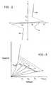
- FIG. 1is a plot of the resistance of a chalcogenide phase-change memory element versus the amplitude of a current pulse through the memory element.
- the resistance of the deviceremains substantially constant (i.e., in its high resistance or RESET state) until a current pulse of sufficient energy is applied.
- the deviceis then transformed from its high resistance (RESET) state to its low resistance (SET) state.
- RESEThigh resistance
- SETlow resistance
- the current pulse sufficient to program the memory element from the high resistance state to the low resistance stateis referred to as a “set pulse”. While not wishing to be bound by theory, it is believed that the set pulse is sufficient to change at least a portion of the volume of memory material from a less-ordered amorphous state to a more-ordered crystalline state.
- the memory devicemay be programmed back from the low resistance state or SET state to the high resistance or RESET state by applying a current pulse of sufficient amplitude, referred to as a “reset pulse”. While not wishing to be bound by theory, it is believed that application of a reset pulse to the memory element is sufficient to change at least a portion of the volume of memory material from a more-ordered crystalline state to a less-ordered amorphous state.
- the memory devicemay be programmed back and forth between the high resistance or RESET state and the low resistance or SET state. This type of programming scheme provides for a binary mode of operation (for example, the RESET state may be a logic 0 while the SET state may be a logic 1).
- the phase-change memory elementmay be programmed to any resistance value within a window of resistance values bounded by the low resistance or SET state and the high resistance or RESET state. More specifically, in this regime along the right side of the curve, the phase-change memory element may be programmed from any one of the resistance states on the right side of the resistance curve to any other of the resistance states on the right side of the curve by the application of a current pulse of sufficient amplitude.
- the devicemay thus be programmed between three or more resistance values within the resistance window so as to provide for multi-state, directly overwritable data storage. While not wishing to be bound by theory, it is believed that each of the resistance states along the right side of the curve may correspond to a particular ratio of the volume of crystalline material to the volume of amorphous material in an active region of the phase-change material. Three intermediate resistance states R 1 , R 2 and R 3 are shown in the resistance curve of FIG. 1.
- a phase-change memory elementis programmed to a particular resistance state (for example, this may be the low resistance or SET state, high resistance or RESET state, or some intermediate state between the SET/RESET states such as R 1 , R 2 or R 3 )
- the particular resistance value of the resistance statemay drift over time. Such drift may create a problem in distinguishing one resistance state from another, especially when the memory device is operated in a multi-state mode. While not wishing to be bound by theory, it is believed that this drift may be due to mechanical stresses caused by the programming of the device as well as the release of these mechanical stresses. A method of operating the memory device is needed which can eliminate the effects of this drift.
- One aspect of the present inventionis a method of operating an electrically programmable, phase-change memory element, the memory element programmable to a plurality of resistance states, the method comprising the step of: applying an electrical signal to the memory element, the electrical signal being insufficient to program the memory element from any of the resistance states to another of second of the resistance states, the electrical signal sufficient to provide a voltage across the memory element having a magnitude which is greater than or equal to the magnitude of the threshold voltage of the memory element.
- Another aspect of the present inventionis a method of reading an electrically programmable, phase-change memory element, the method comprising the steps of: applying a first electrical signal to the memory element, the first electrical signal causing a first voltage across the memory element, the first voltage having a magnitude greater than or equal to the magnitude of the threshold voltage of the memory element; and applying a second electrical signal to the memory element, the second electrical signal causing a second voltage across the memory element, the second voltage having a magnitude less than the magnitude of the threshold voltage of the memory element.
- Another aspect of the inventionis a method of operating an electrically programmable, phase-change memory element, the memory element programmable to a plurality of resistance states, the method comprising the step of:
- FIG. 1shows an example of a resistance curve of a chalcogenide-based phase-change memory element
- FIG. 2is an example of a current-voltage characteristic curve for a chalcogenide-based phase-change memory element
- FIG. 3is an example of a family of current-voltage characteristic curves for a chalcogenide-based phase-change memory element
- FIG. 4Ais an example of a dual voltage scheme for reading the resistance state of a phase-change memory element
- FIG. 4Bis an example of a dual voltage scheme for reading the resistance state of a phase-change memory element
- FIG. 5Ais an example of a dual current scheme for reading the resistance state of a phase-change memory element
- FIG. 5Bis an example of a dual current scheme for reading the resistance state of a phase-change memory element.
- FIG. 6is a plot showing that application of a current of sufficient amplitude to the memory element can cause the memory element to return to its pre-drift resistance value.
- the novel methodcomprises the step of applying an electrical signal to the memory element.
- the electrical signalis sufficient to cause a voltage across the memory element having a magnitude which is greater than magnitude of the threshold voltage of the element.
- the electrical signalis insufficient to program the memory element from any one of its resistance states to any other of its resistance states.
- the electrical signalmay be applied as a controlled current (such as from a current source) or as a controlled voltage (such as from a voltage source). It is noted that as used herein the terminology “memory element” and “memory device” are synonymous and are used interchangeably.
- a chalcogenide phase-change memory elementmay be programmed to different resistance states. Associated with a chalcogenide phase-change memory element in a particular resistance state is a current-voltage, or “I-V”, characteristic curve.
- I-V characteristic curvedescribes the relationship between the current through the memory device as a function of the voltage across the device.
- the I-V characteristic curvedescribes the electrical switching behavior of the memory element in its particular resistance state as the voltage across the device is increased.
- FIG. 2shows the I-V plot in both the first quadrant (where voltages and currents are positive) and the third quadrant (where voltages and currents are negative). While only the first quadrant is described below, an analogous description applies to the curve in the third quadrant of the I-V plot (where the voltage and the current are both negative).
- the I-V characteristic curve IVincludes an “off-state” branch 50 and an “on-state” branch 60 .
- the off-state branch 50corresponds to the branch in which the current passing through the memory device increases slightly upon increasing the voltage applied across the memory device. This branch exhibits a small slope in the I-V plot and appears as a nearly horizontal line in the first (and third) quadrant of FIG. 2.
- the on-state branch 60corresponds to the branch in which the current passing through the memory device increases significantly upon increasing the voltage applied across the memory device.
- the magnitude of the slope of the on-state branchis greater than the magnitude of the slope of the off-state branch. In the example shown in FIG.
- the on-state branchexhibits a large slope in the I-V plot and appears as a substantially vertical line in the first (and third) quadrant of FIG. 2.
- the slopes of the off-state and on-state branches shown in FIG. 2are illustrative and not intended to be limiting. Regardless of the actual slopes, the on-state branch exhibits a steeper slope than the off-state branch.
- the switching properties of the memory elementcan be described by reference to FIG. 2.
- the memory elementremains in the OFF state as the voltage across the memory element and the current through the memory element is increased, up to a voltage V t which is referred to as the “threshold voltage” of the memory element.
- V tvoltage which is referred to as the “threshold voltage” of the memory element.
- the memory deviceswitches from the off-state branch 50 to the on-state branch 60 of the I-V curve.
- the switching eventoccurs instantaneously and is depicted by the dashed line in FIG. 2.
- branch 60is steeper than branch 50 .
- the memory deviceremains in the on-state branch 60 as long as a minimum current, labeled I h in FIG. 2, is maintained.
- I his referred to as the holding current of the memory device and the associated voltage V h is referred to as the holding voltage of the memory device.
- the memory elementIf the memory element conditions are changed so that the current becomes less than I h , the memory element normally returns to the off-state branch 50 of the I-V plot and requires re-application of a voltage which is greater than or equal to the threshold voltage V t to resume operation on the on-state branch. If the current is only momentarily (a time less than the recovery time of the chalcogenide material) reduced below I h , the ON state of the memory element may be recovered upon restoring the current through the memory element which is at or above I h . The recovery time of devices made with chalcogenide materials has been discussed in the article “Amorphous Semiconductors for Switching, Memory, and Imaging Applications” incorporated by reference herein.
- Analogous switching behavioroccurs in the third quadrant of the I-V plot shown in FIG. 2.
- the switching behavior in the third quadrantis analogous to that described hereinabove for the first quadrant.
- applied voltages having a magnitude greater than the magnitude of the negative threshold voltage in the third quadrantinduce switching from the off-state branch 50 to the on-state branch 60 .
- the memory elementmay be switched from an OFF state to an ON state by application of a voltage across the memory element having a magnitude which is greater than or equal to the magnitude of the threshold voltage V t .
- a voltage across the memory elementwhich is at or above the threshold voltage may cause the formation of a conductive channel or filament within the chalcogenide memory material.
- the electric field experienced by the chalcogenide materialis sufficiently high to induce a breakdown or avalanche effect whereby electrons are removed from atoms to form a highly conductive, plasma-like filament of charge carriers. Rather than being bound to atoms, some electrons become unbound and highly mobile.
- a conductive channel or filamentforms.
- the conductive filamentconstitutes a conductive volume within the otherwise resistive chalcogenide material.
- the conductive filamentextends through the chalcogenide material between the device terminals and provides a low resistance pathway for electrical current. Portions of the chalcogenide material outside of the filament remain resistive. Since electric current traverses the path of least resistance, the presence of a conductive filament renders the chalcogenide material more conductive and establishes an “ON” state.
- the creation of a conductive filamentis the event that underlies the switching of the chalcogenide memory element from its OFF state to its ON state.
- the current-voltage (I-V) characteristics of a memory elementis dependent upon the resistance state of the memory element. As the memory element is programmed to different resistance states, the I-V characteristics as well as the associated threshold voltage will change. (As noted above, each resistance state may correspond to a different ratio of crystalline to amorphous material in an active portion of the chalcogenide memory material of the memory element. As the ratio of crystalline to amorphous material changes, so does the corresponding current-voltage characteristics and threshold voltage of the memory element).
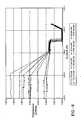
- FIG. 3shows an I-V curve IV SET that describes the current-voltage characteristics of the device in its low resistance or SET state as well as I-V curve IV RESET that describes the current-voltage characteristics of the device in its high resistance or RESET state.
- FIG. 3also shows I-V curves IV R1 , IV R2 and IV R3 describe the current-voltage characteristics for the device in its resistance states R 1 , R 2 and R 3 , respectively, along the right hand side of the resistance curve shown in FIG.
- a threshold voltage V texists for each resistance state of the device except for the SET state.
- the threshold voltage V tvaries with the resistance state so that a different threshold voltage V t1 , V t2 , V t3 , V tRESET corresponds to a respective resistance state R 1 , R 2 , R 3 and RESET.
- the threshold voltage V tincreases with increasing resistance of the resistance state.
- the I-V characteristic curves shown in FIG. 3are symmetric with respect to the polarity of the applied voltage (that is, negative voltages cause negative currents). However, for convenience, only the first quadrant (where voltages and currents are positive) of the I-V plots are shown.
- the threshold voltage V t of the deviceis thus dependent upon the actual resistance state of the device.
- the threshold voltage V tmay also depend upon other factors such as the thickness of the memory device as well as the actual chalcogenide composition used.
- the inventors of the present inventionhave discovered that switching the memory element from its OFF state to its ON state is sufficient to reverse the effects of resistance drift and return the memory element to its pre-drift programmed resistance state.
- the devicemay be switched by the application of a voltage across the memory element having a magnitude which greater than or equal to the magnitude of the threshold voltage of the memory element.
- the memory devicemay be forced to return to its pre-drift resistance state by application of a voltage across the memory element having a magnitude which is greater than or equal to the threshold voltage of the memory element. This voltage is referred to as the “drift recovery” voltage V DR .
- a voltage V DR having a magnitude greater than or equal to the magnitude of the threshold voltagemay be applied across the memory element by applying an appropriate electrical signal to the memory element.
- the electrical signalmay be a controlled voltage signal (such as from a voltage source).
- the electrical signalmay be in the form of a controlled voltage pulse from a voltage source where the controlled voltage pulse has an amplitude V RD greater than or equal to the amplitude of the threshold voltage.
- the electrical signalmay be in the form of a controlled current (such as from a current source) directed through the memory element.
- the electrical signalmay be in the form of a controlled current pulse from a current source where the controlled current pulse has an amplitude which is greater than or equal to the magnitude of current needed to cause the voltage across the memory element to reach the threshold voltage V t .
- the magnitude of current needed to cause the voltage across the memory element to reach the threshold voltageis shown in FIG. 2 as the current I t .
- the electrical signal used for drift recoveryshould preferably be insufficient to program the memory element away from its present resistance state to any other resistance state.
- the current through the memory element as a result of this electrical signalshould preferably be insufficient to program the memory element from any one of the resistance states of the memory element to any other of the resistance states of the memory element.
- the current through the memory element as a result of the applied drift recovery electrical signalhas a magnitude which is less than about one-third of the magnitude of the current needed to program the memory element to another resistance state.
- the magnitude of the currentis preferably less than about one-third the current needed to program the memory element to its low resistance or SET state.
- a current through the memory element having a magnitude between about 5 micro-amps and about 20 micro-ampsmay be sufficient to reverse the effects of resistance drift.
- the drift recovery electrical signal applied to the memory element for reversing the effects of resistance driftis preferably in the form of a pulse with a finite pulse width.
- the width of the pulseis preferably greater than about 5 nanoseconds. More preferably, the width of the pulse is between about 5 nanoseconds and about 20 nanoseconds. However, other widths are also possible and the present invention is not limited to any particular width.
- the actual width usedmay depend upon the width of the read pulse used to actually read the resistance of the memory element.
- the width of the drift recovery pulseis less than the width of the read pulse used for reading the resistance of the memory element.
- the drift recovery pulsemay have any shape. For example, it may have a substantially constant amplitude (such as a square pulse). Alternately, it may have a varying amplitude.
- the devicemay be read by applying a controlled voltage across the device (such as from a voltage source) having a magnitude which is preferably below the magnitude of the threshold voltage of the device and then measuring the current through the device. The lower the measured current, the higher the resistance state of the device. Alternately, the device may be read by applying a controlled current through the device (such as from a current source) and measuring the voltage across the device.
- a controlled voltage across the devicesuch as from a voltage source
- a controlled current through the devicesuch as from a current source
- a possible scheme for accurately reading the resistance state of the devicemay thus be to apply a first voltage V 1 across the device which is at least as large as the device threshold voltage so as to cause the device to return to its pre-drift resistance state.
- the corresponding current through the memory elementshould be insufficient to program the device from its present resistance state to a different resistance state.
- This first voltage V 1is followed by a second voltage V 2 which is less than the threshold voltage V t of the device.
- This second voltage V 2will actually be used to measure the resistance state of the device.
- FIGS. 4A and 4BAn example of this dual voltage scheme is shown in FIGS. 4A and 4B.
- a second voltage V 2immediately follows the first voltage V 1 .
- FIG. 4Aa second voltage V 2 immediately follows the first voltage V 1 .
- the application of a second voltage pulse V 2follows the end of a first voltage pulse V 1 .
- any delay between a first and a second voltage pulseshould be sufficiently small so that drift in the resistance state does not re-occur to any significant extent.
- the duration of the first voltage pulse V 1(the drift recovery pulse) is preferably less than the duration of the second voltage pulse V 2 (the read pulse).
- a reading schememay be described in terms of currents applied through the memory element.
- a first current I 1may be applied through the device which is greater than or equal to a current I t where I t is a current needed to create a threshold voltage V t across the device.
- I 1should be less then a current which may program the device to another resistance state.
- the first current I 1is used for drift recovery. That is, to force the device back to its pre-drift resistance state.
- This first current I 1is followed by a second current 12 which is less than I t .
- This second current I 2is used to actually measure the pre-drift resistance state of the memory element. That is, to read the value of the resistance state.
- a known current I 2may be applied through the memory element and the corresponding voltage across the memory element may then be measured.
- An example of this dual current schemeis shown in FIGS. 5A and 5B.
- a second current I 2immediately follows the first current I 1 .
- the application of a second current pulse I 2follows the first current pulse I 1 .
- any delay between the first and second current pulsesshould be sufficiently small so that drift in the resistance state does not re-occur to any significant extent.
- the duration of the first current pulse I 1(the drift recovery pulse) is preferably less than the duration of the second current pulse I 2 (the read pulse).
- a programmable phase-change memory element having a memory material with the composition Te 2 Ge 2 Sb 5is programmed to its high resistance or RESET state.
- the memory element resistanceis allowed to drift for a time period of 0.1 minute.
- the memory elementdrifts to a resistance that is greater than the resistance of the RESET state.
- a current having an amplitude of about 8 micro-ampsis directed through the memory element which causes the memory element to return to its pre-drift RESET resistance value.
- the same experimentis repeated whereby the resistance of the memory element is allowed to drift for progressively longer time periods of 1 minute, 12 minutes, 60 minutes, 116 minutes, 180 minutes, 1140 minutes, and 2730 minutes.
- the resistance of the memory elementdrifts to increasingly higher values. For each case, a current of approximately 8 to 12 micro-amps directed through the memory element is sufficient to return the memory element to its pre-drift resistance.
- the present inventionrelates to phase-change memory elements.
- the phase-change memory elementincludes a phase-change memory material which is preferably formed from a plurality of constituent atomic elements.
- the phase-change materialincludes one or more elements selected from the group consisting of Te, Se, Ge, Sb, Bi, Pb, Sn, As, S, Si, P, O and mixtures or alloys thereof.
- the phase-change materialpreferably includes at least one chalcogen element.
- the at least one chalcogen elementis selected from the group consisting of Te, Se and mixtures or alloys thereof.
- the at least one chalcogen elementmay be a mixture of Te and Se.
- the memory materialis a ternary Ge—Sb—Te alloy.
- An example of a phase-change materialis the chalcogenide composition Ge 2 Sb 2 Te 5
- the phase-change materialmay include at least one transition metal element.
- transition metalas used herein includes elements 21 to 30, 39 to 48, 57 and 72 to 80.
- the transition metal elementis selected from the group consisting of Cr, Fe, Ni, Nb, Pd, Pt and mixtures or alloys thereof. Most preferably the transition metal is Ni. Specific examples of such multi-element systems are set forth hereinafter with respect to the Te:Ge:Sb system with or without Ni and/or Se.
- the phase-change materials which include transition metalsare elementally modified forms of the phase-change materials in the Te—Ge—Sb ternary system. That is, the elementally modified phase-change materials constitute modified forms of the Ge—Sb—Te phase-change alloys. This elemental modification is achieved by the incorporation of transition metals into the basic Ge—Sb—Te ternary system, with or without an additional chalcogen element, such as Se.
- the memory elementincludes means for applying energy to the memory material.
- the memory elementmay include one or more electrodes for supplying the electrical signal to the memory material.
- the shape of the electrodes as well as their positioning relative to the volume of memory materialmay be varied to form different device structures.
- the electrodesmay include first and second electrodes positioned adjacent to the memory material.
Landscapes
- Chemical & Material Sciences (AREA)
- Crystallography & Structural Chemistry (AREA)
- Semiconductor Memories (AREA)
Abstract
Description
- The present invention relates generally to electrically programmable phase-change memory. More specifically, the present invention relates to methods of eliminating drift in electrical programmable phase-change memory.[0001]
- The use of electrically programmable phase-change materials (for example, materials which can be electrically programmed between amorphous and crystalline states) for electronic memory applications is well known in the art and is disclosed, for example, in commonly assigned U.S. Pat. Nos. 5,166,758, 5,296,716, 5,414,271, 5,359,205, 5,341,328, 5,536,947, 5,534,712, 5,687,112, and 5,825,046 the disclosures of which are all incorporated by reference herein. Still another example of a phase-change memory element is provided in commonly assigned U.S. patent application Ser. No. 09/276,273, the disclosure of which is incorporated by reference herein.[0002]
- Generally, phase-change materials are capable of being electrically programmed between a first structural state having a where the material is generally amorphous and a second structural state where the material is generally crystalline. The term “amorphous”, as used herein, refers to a condition which is relatively structurally less ordered or more disordered than a single crystal. The term “crystalline”, as used herein, refers to a condition which is relatively structurally more ordered than amorphous. The phase-change material exhibits different electrical characteristics depending upon its state. For instance, in its crystalline, more ordered state the material exhibits a lower electrical resistivity than in its amorphous, less ordered state.[0003]
- Materials that may be used as a phase-change material include alloys of the elements from group VI of the Periodic Table. These group VI elements are referred to as the chalcogen elements and include the elements Te and Se. Alloys that include one or more of the chalcogen elements are referred to as chalcogenide alloys. An example of a chalcogenide alloy is the alloy Ge[0004]2Sb2Te5.
- FIG. 1 is a plot of the resistance of a chalcogenide phase-change memory element versus the amplitude of a current pulse through the memory element. Referring to FIG. 1, several different programming regimes can be distinguished. In the left side of the curve, the resistance of the device remains substantially constant (i.e., in its high resistance or RESET state) until a current pulse of sufficient energy is applied. The device is then transformed from its high resistance (RESET) state to its low resistance (SET) state. The current pulse sufficient to program the memory element from the high resistance state to the low resistance state is referred to as a “set pulse”. While not wishing to be bound by theory, it is believed that the set pulse is sufficient to change at least a portion of the volume of memory material from a less-ordered amorphous state to a more-ordered crystalline state.[0005]
- The memory device may be programmed back from the low resistance state or SET state to the high resistance or RESET state by applying a current pulse of sufficient amplitude, referred to as a “reset pulse”. While not wishing to be bound by theory, it is believed that application of a reset pulse to the memory element is sufficient to change at least a portion of the volume of memory material from a more-ordered crystalline state to a less-ordered amorphous state. The memory device may be programmed back and forth between the high resistance or RESET state and the low resistance or SET state. This type of programming scheme provides for a binary mode of operation (for example, the RESET state may be a[0006]
logic 0 while the SET state may be a logic 1). - Referring to the right side of the curve of FIG. 1, as the amplitude of the current through the memory element increases, the resistance of the device increases. This increase is both gradual and reversible. In this regime, the phase-change memory element may be programmed to any resistance value within a window of resistance values bounded by the low resistance or SET state and the high resistance or RESET state. More specifically, in this regime along the right side of the curve, the phase-change memory element may be programmed from any one of the resistance states on the right side of the resistance curve to any other of the resistance states on the right side of the curve by the application of a current pulse of sufficient amplitude. The device may thus be programmed between three or more resistance values within the resistance window so as to provide for multi-state, directly overwritable data storage. While not wishing to be bound by theory, it is believed that each of the resistance states along the right side of the curve may correspond to a particular ratio of the volume of crystalline material to the volume of amorphous material in an active region of the phase-change material. Three intermediate resistance states R[0007]1, R2 and R3 are shown in the resistance curve of FIG. 1.
- After a phase-change memory element is programmed to a particular resistance state (for example, this may be the low resistance or SET state, high resistance or RESET state, or some intermediate state between the SET/RESET states such as R[0008]1, R2 or R3), the particular resistance value of the resistance state may drift over time. Such drift may create a problem in distinguishing one resistance state from another, especially when the memory device is operated in a multi-state mode. While not wishing to be bound by theory, it is believed that this drift may be due to mechanical stresses caused by the programming of the device as well as the release of these mechanical stresses. A method of operating the memory device is needed which can eliminate the effects of this drift.
- One aspect of the present invention is a method of operating an electrically programmable, phase-change memory element, the memory element programmable to a plurality of resistance states, the method comprising the step of: applying an electrical signal to the memory element, the electrical signal being insufficient to program the memory element from any of the resistance states to another of second of the resistance states, the electrical signal sufficient to provide a voltage across the memory element having a magnitude which is greater than or equal to the magnitude of the threshold voltage of the memory element.[0009]
- Another aspect of the present invention is a method of reading an electrically programmable, phase-change memory element, the method comprising the steps of: applying a first electrical signal to the memory element, the first electrical signal causing a first voltage across the memory element, the first voltage having a magnitude greater than or equal to the magnitude of the threshold voltage of the memory element; and applying a second electrical signal to the memory element, the second electrical signal causing a second voltage across the memory element, the second voltage having a magnitude less than the magnitude of the threshold voltage of the memory element.[0010]
- Another aspect of the invention is a method of operating an electrically programmable, phase-change memory element, the memory element programmable to a plurality of resistance states, the method comprising the step of:[0011]
- applying an electrical signal to the memory element, the electrical signal being insufficient to program the memory element from any one of the resistance states to any other of the resistance states, the electrical signal sufficient to switch the memory element from its OFF state to its ON state.[0012]
- FIG. 1 shows an example of a resistance curve of a chalcogenide-based phase-change memory element;[0013]
- FIG. 2 is an example of a current-voltage characteristic curve for a chalcogenide-based phase-change memory element;[0014]
- FIG. 3 is an example of a family of current-voltage characteristic curves for a chalcogenide-based phase-change memory element;[0015]
- FIG. 4A is an example of a dual voltage scheme for reading the resistance state of a phase-change memory element;[0016]
- FIG. 4B is an example of a dual voltage scheme for reading the resistance state of a phase-change memory element;[0017]
- FIG. 5A is an example of a dual current scheme for reading the resistance state of a phase-change memory element;[0018]
- FIG. 5B is an example of a dual current scheme for reading the resistance state of a phase-change memory element; and[0019]
- FIG. 6 is a plot showing that application of a current of sufficient amplitude to the memory element can cause the memory element to return to its pre-drift resistance value.[0020]
- Disclosed herein is a novel method of operating a phase-change memory element. The novel method comprises the step of applying an electrical signal to the memory element. The electrical signal is sufficient to cause a voltage across the memory element having a magnitude which is greater than magnitude of the threshold voltage of the element. However, the electrical signal is insufficient to program the memory element from any one of its resistance states to any other of its resistance states. The electrical signal may be applied as a controlled current (such as from a current source) or as a controlled voltage (such as from a voltage source). It is noted that as used herein the terminology “memory element” and “memory device” are synonymous and are used interchangeably.[0021]
- As noted above, a chalcogenide phase-change memory element may be programmed to different resistance states. Associated with a chalcogenide phase-change memory element in a particular resistance state is a current-voltage, or “I-V”, characteristic curve. The I-V characteristic curve describes the relationship between the current through the memory device as a function of the voltage across the device. In addition, the I-V characteristic curve describes the electrical switching behavior of the memory element in its particular resistance state as the voltage across the device is increased.[0022]
- An example of an I-V characteristic curve for a chalcogenide memory element in a particular resistance state is shown in FIG. 2. FIG. 2 shows the I-V plot in both the first quadrant (where voltages and currents are positive) and the third quadrant (where voltages and currents are negative). While only the first quadrant is described below, an analogous description applies to the curve in the third quadrant of the I-V plot (where the voltage and the current are both negative).[0023]
- The I-V characteristic curve IV includes an “off-state”[0024]
branch 50 and an “on-state”branch 60. The off-state branch 50 corresponds to the branch in which the current passing through the memory device increases slightly upon increasing the voltage applied across the memory device. This branch exhibits a small slope in the I-V plot and appears as a nearly horizontal line in the first (and third) quadrant of FIG. 2. The on-state branch 60 corresponds to the branch in which the current passing through the memory device increases significantly upon increasing the voltage applied across the memory device. The magnitude of the slope of the on-state branch is greater than the magnitude of the slope of the off-state branch. In the example shown in FIG. 2, the on-state branch exhibits a large slope in the I-V plot and appears as a substantially vertical line in the first (and third) quadrant of FIG. 2. The slopes of the off-state and on-state branches shown in FIG. 2 are illustrative and not intended to be limiting. Regardless of the actual slopes, the on-state branch exhibits a steeper slope than the off-state branch. When conditions are such that the current through the device and voltage across the device is described by a point on the off-state branch of the I-V curve, the memory device is said to be in the “OFF” state. Likewise, when conditions are such that the current through the device and voltage across the device is described by a point on the on-state branch of the I-V curve, the memory device is said to be in the “ON” state. - The switching properties of the memory element (in a particular resistance state) can be described by reference to FIG. 2. When no voltage is applied across the device, the device is in the “OFF” state and no current flows. This condition corresponds to the origin of the I-V plot shown in FIG. 2 (current=0, voltage=0). The memory element remains in the OFF state as the voltage across the memory element and the current through the memory element is increased, up to a voltage V[0025]twhich is referred to as the “threshold voltage” of the memory element. When the voltage across the memory element is less than Vt, the slope of the off-state branch of the I-V curve is small and the current flowing through the memory element increases only in a small amount as the applied voltage is increased.
- When the applied voltage across the device equals or exceeds the threshold voltage V[0026]t, the memory device switches from the off-
state branch 50 to the on-state branch 60 of the I-V curve. The switching event occurs instantaneously and is depicted by the dashed line in FIG. 2. Upon switching, the voltage across the device decreases significantly and the current through the device becomes much more sensitive to changes in the device voltage (hence,branch 60 is steeper than branch50). The memory device remains in the on-state branch 60 as long as a minimum current, labeled Ihin FIG. 2, is maintained. Ihis referred to as the holding current of the memory device and the associated voltage Vhis referred to as the holding voltage of the memory device. If the memory element conditions are changed so that the current becomes less than Ih, the memory element normally returns to the off-state branch 50 of the I-V plot and requires re-application of a voltage which is greater than or equal to the threshold voltage Vtto resume operation on the on-state branch. If the current is only momentarily (a time less than the recovery time of the chalcogenide material) reduced below Ih, the ON state of the memory element may be recovered upon restoring the current through the memory element which is at or above Ih. The recovery time of devices made with chalcogenide materials has been discussed in the article “Amorphous Semiconductors for Switching, Memory, and Imaging Applications” incorporated by reference herein. - Analogous switching behavior occurs in the third quadrant of the I-V plot shown in FIG. 2. Provided one is aware of the negative polarities of both the voltage and current of the I-V curve in the third quadrant, the switching behavior in the third quadrant is analogous to that described hereinabove for the first quadrant. For example, applied voltages having a magnitude greater than the magnitude of the negative threshold voltage in the third quadrant induce switching from the off-[0027]
state branch 50 to the on-state branch 60. - Hence, as described above, the memory element may be switched from an OFF state to an ON state by application of a voltage across the memory element having a magnitude which is greater than or equal to the magnitude of the threshold voltage V[0028]t. While not wishing to be bound by theory, it is believed that application of a voltage across the memory element which is at or above the threshold voltage may cause the formation of a conductive channel or filament within the chalcogenide memory material. At the threshold voltage Vt, the electric field experienced by the chalcogenide material is sufficiently high to induce a breakdown or avalanche effect whereby electrons are removed from atoms to form a highly conductive, plasma-like filament of charge carriers. Rather than being bound to atoms, some electrons become unbound and highly mobile. As a result, a conductive channel or filament forms. The conductive filament constitutes a conductive volume within the otherwise resistive chalcogenide material. The conductive filament extends through the chalcogenide material between the device terminals and provides a low resistance pathway for electrical current. Portions of the chalcogenide material outside of the filament remain resistive. Since electric current traverses the path of least resistance, the presence of a conductive filament renders the chalcogenide material more conductive and establishes an “ON” state. The creation of a conductive filament is the event that underlies the switching of the chalcogenide memory element from its OFF state to its ON state.
- The current-voltage (I-V) characteristics of a memory element, including the threshold voltage V[0029]t, is dependent upon the resistance state of the memory element. As the memory element is programmed to different resistance states, the I-V characteristics as well as the associated threshold voltage will change. (As noted above, each resistance state may correspond to a different ratio of crystalline to amorphous material in an active portion of the chalcogenide memory material of the memory element. As the ratio of crystalline to amorphous material changes, so does the corresponding current-voltage characteristics and threshold voltage of the memory element).
- Associated with a memory element is a family of I-V curves where each curve corresponds to a particular resistance state of the memory element. An example of a family of I-V curves is shown in FIG. 3. FIG. 3 shows an I-V curve IV[0030]SETthat describes the current-voltage characteristics of the device in its low resistance or SET state as well as I-V curve IVRESETthat describes the current-voltage characteristics of the device in its high resistance or RESET state. FIG. 3 also shows I-V curves IVR1, IVR2and IVR3describe the current-voltage characteristics for the device in its resistance states R1, R2 and R3, respectively, along the right hand side of the resistance curve shown in FIG. 1 (where R3 resistance>R2 resistance>R1 resistance>SET resistance). As seen from FIG. 3, a threshold voltage Vtexists for each resistance state of the device except for the SET state. In addition, it is seen that the threshold voltage Vtvaries with the resistance state so that a different threshold voltage Vt1, Vt2, Vt3, VtRESETcorresponds to a respective resistance state R1, R2, R3 and RESET. As shown in FIG. 3, the threshold voltage Vtincreases with increasing resistance of the resistance state. The I-V characteristic curves shown in FIG. 3 are symmetric with respect to the polarity of the applied voltage (that is, negative voltages cause negative currents). However, for convenience, only the first quadrant (where voltages and currents are positive) of the I-V plots are shown.
- The threshold voltage V[0031]tof the device is thus dependent upon the actual resistance state of the device. In addition, the threshold voltage Vtmay also depend upon other factors such as the thickness of the memory device as well as the actual chalcogenide composition used.
- The inventors of the present invention have discovered that switching the memory element from its OFF state to its ON state is sufficient to reverse the effects of resistance drift and return the memory element to its pre-drift programmed resistance state. As noted above, the device may be switched by the application of a voltage across the memory element having a magnitude which greater than or equal to the magnitude of the threshold voltage of the memory element. Hence, the memory device may be forced to return to its pre-drift resistance state by application of a voltage across the memory element having a magnitude which is greater than or equal to the threshold voltage of the memory element. This voltage is referred to as the “drift recovery” voltage V[0032]DR.
- It is believed that programming a memory element from one resistance state to another resistance state may introduce a stress into the memory element and that the relaxation of this stress that may cause resistance drift. While not wishing to be bound by theory, it is believed that switching the memory element from its OFF state to its ON state may reintroduce stress into the memory element so as to force the memory element to return to its pre-drift resistance state.[0033]
- A voltage V[0034]DRhaving a magnitude greater than or equal to the magnitude of the threshold voltage may be applied across the memory element by applying an appropriate electrical signal to the memory element. The electrical signal may be a controlled voltage signal (such as from a voltage source). For example, the electrical signal may be in the form of a controlled voltage pulse from a voltage source where the controlled voltage pulse has an amplitude VRDgreater than or equal to the amplitude of the threshold voltage.
- Alternately, the electrical signal may be in the form of a controlled current (such as from a current source) directed through the memory element. For example, the electrical signal may be in the form of a controlled current pulse from a current source where the controlled current pulse has an amplitude which is greater than or equal to the magnitude of current needed to cause the voltage across the memory element to reach the threshold voltage V[0035]t. The magnitude of current needed to cause the voltage across the memory element to reach the threshold voltage is shown in FIG. 2 as the current It.
- Regardless of the form of the electrical signal applied to the memory device, the electrical signal used for drift recovery should preferably be insufficient to program the memory element away from its present resistance state to any other resistance state. Hence, the current through the memory element as a result of this electrical signal should preferably be insufficient to program the memory element from any one of the resistance states of the memory element to any other of the resistance states of the memory element. Preferably, the current through the memory element as a result of the applied drift recovery electrical signal has a magnitude which is less than about one-third of the magnitude of the current needed to program the memory element to another resistance state. The magnitude of the current is preferably less than about one-third the current needed to program the memory element to its low resistance or SET state. As an example, for certain memory elements, it is possible that a current through the memory element having a magnitude between about 5 micro-amps and about 20 micro-amps may be sufficient to reverse the effects of resistance drift.[0036]
- The drift recovery electrical signal applied to the memory element for reversing the effects of resistance drift is preferably in the form of a pulse with a finite pulse width. The width of the pulse is preferably greater than about 5 nanoseconds. More preferably, the width of the pulse is between about 5 nanoseconds and about 20 nanoseconds. However, other widths are also possible and the present invention is not limited to any particular width. The actual width used may depend upon the width of the read pulse used to actually read the resistance of the memory element. Preferably, the width of the drift recovery pulse is less than the width of the read pulse used for reading the resistance of the memory element. In addition, the drift recovery pulse may have any shape. For example, it may have a substantially constant amplitude (such as a square pulse). Alternately, it may have a varying amplitude.[0037]
- Hence, by applying an electrical signal to the memory element that (1) returns the device to its pre-drift condition and (2) does not program the device to a different resistance state, it thus becomes possible to then accurately read the resistance state of the device whether the device is operating in a binary mode (for example, by being programmed back and forth between its low resistance state and high resistance state) or whether the device is operating in a multi-state mode (for example, by being programmed between three or more resistance states along the right side of the resistance curve shown in FIG. 1).[0038]
- The device may be read by applying a controlled voltage across the device (such as from a voltage source) having a magnitude which is preferably below the magnitude of the threshold voltage of the device and then measuring the current through the device. The lower the measured current, the higher the resistance state of the device. Alternately, the device may be read by applying a controlled current through the device (such as from a current source) and measuring the voltage across the device.[0039]
- Hence, a possible scheme for accurately reading the resistance state of the device may thus be to apply a first voltage V[0040]1across the device which is at least as large as the device threshold voltage so as to cause the device to return to its pre-drift resistance state. The corresponding current through the memory element should be insufficient to program the device from its present resistance state to a different resistance state. This first voltage V1is followed by a second voltage V2which is less than the threshold voltage Vtof the device. This second voltage V2will actually be used to measure the resistance state of the device. An example of this dual voltage scheme is shown in FIGS. 4A and 4B. In FIG. 4A, a second voltage V2immediately follows the first voltage V1. In FIG. 4B, the application of a second voltage pulse V2follows the end of a first voltage pulse V1. Preferably, any delay between a first and a second voltage pulse should be sufficiently small so that drift in the resistance state does not re-occur to any significant extent. As noted above, the duration of the first voltage pulse V1(the drift recovery pulse) is preferably less than the duration of the second voltage pulse V2(the read pulse).
- A reading scheme may be described in terms of currents applied through the memory element. For example, a first current I[0041]1may be applied through the device which is greater than or equal to a current Itwhere Itis a current needed to create a threshold voltage Vtacross the device. However, I1should be less then a current which may program the device to another resistance state. The first current I1is used for drift recovery. That is, to force the device back to its pre-drift resistance state. This first current I1is followed by a second current12 which is less than It. This second current I2is used to actually measure the pre-drift resistance state of the memory element. That is, to read the value of the resistance state. For example, a known current I2may be applied through the memory element and the corresponding voltage across the memory element may then be measured. An example of this dual current scheme is shown in FIGS. 5A and 5B. In FIG. 5A, a second current I2immediately follows the first current I1. In FIG. 5B, the application of a second current pulse I2follows the first current pulse I1. Preferably, any delay between the first and second current pulses should be sufficiently small so that drift in the resistance state does not re-occur to any significant extent. The duration of the first current pulse I1(the drift recovery pulse) is preferably less than the duration of the second current pulse I2(the read pulse).
- A programmable phase-change memory element having a memory material with the composition Te[0042]2Ge2Sb5is programmed to its high resistance or RESET state. The memory element resistance is allowed to drift for a time period of 0.1 minute. As shown in FIG. 6, the memory element drifts to a resistance that is greater than the resistance of the RESET state. A current having an amplitude of about 8 micro-amps is directed through the memory element which causes the memory element to return to its pre-drift RESET resistance value. The same experiment is repeated whereby the resistance of the memory element is allowed to drift for progressively longer time periods of 1 minute, 12 minutes, 60 minutes, 116 minutes, 180 minutes, 1140 minutes, and 2730 minutes. As the period of drift time increases, the resistance of the memory element drifts to increasingly higher values. For each case, a current of approximately 8 to 12 micro-amps directed through the memory element is sufficient to return the memory element to its pre-drift resistance.
- The present invention relates to phase-change memory elements. The phase-change memory element includes a phase-change memory material which is preferably formed from a plurality of constituent atomic elements. Preferably, the phase-change material includes one or more elements selected from the group consisting of Te, Se, Ge, Sb, Bi, Pb, Sn, As, S, Si, P, O and mixtures or alloys thereof. The phase-change material preferably includes at least one chalcogen element. Preferably, the at least one chalcogen element is selected from the group consisting of Te, Se and mixtures or alloys thereof. The at least one chalcogen element may be a mixture of Te and Se. Preferably, the memory material is a ternary Ge—Sb—Te alloy. An example of a phase-change material is the chalcogenide composition Ge[0043]2Sb2Te5
- The phase-change material may include at least one transition metal element. The term “transition metal” as used herein includes elements 21 to 30, 39 to 48, 57 and 72 to 80. Preferably, the transition metal element is selected from the group consisting of Cr, Fe, Ni, Nb, Pd, Pt and mixtures or alloys thereof. Most preferably the transition metal is Ni. Specific examples of such multi-element systems are set forth hereinafter with respect to the Te:Ge:Sb system with or without Ni and/or Se. The phase-change materials which include transition metals are elementally modified forms of the phase-change materials in the Te—Ge—Sb ternary system. That is, the elementally modified phase-change materials constitute modified forms of the Ge—Sb—Te phase-change alloys. This elemental modification is achieved by the incorporation of transition metals into the basic Ge—Sb—Te ternary system, with or without an additional chalcogen element, such as Se.[0044]
- In addition to a phase-change memory material, the memory element includes means for applying energy to the memory material. When the energy is electrical energy, the memory element may include one or more electrodes for supplying the electrical signal to the memory material. The shape of the electrodes as well as their positioning relative to the volume of memory material may be varied to form different device structures. As an example, the electrodes may include first and second electrodes positioned adjacent to the memory material.[0045]
- It is to be understood that the disclosure set forth herein is presented in the form of detailed embodiments described for the purpose of making a full and complete disclosure of the present invention, and that such details are not to be interpreted as limiting the true scope of this invention as set forth and defined in the appended claims.[0046]
Claims (21)
1. A method of operating an electrically programmable, phase-change memory element, said memory element programmable to a plurality of resistance states, said method comprising the step of:
applying an electrical signal to said memory element, said electrical signal being insufficient to program said memory element from any one of said resistance states to any other of said resistance states, said electrical signal sufficient to cause a voltage across said memory element having a magnitude which is greater than or equal to the magnitude of the threshold voltage of said memory element.
2. The method ofclaim 1 , wherein said electrical signal is from a current source.
3. The method ofclaim 1 , wherein said electrical signal is from a voltage source.
4. The method ofclaim 1 , wherein said electrical signal causes a current through memory element, said current having a magnitude less than about one-third the magnitude of current needed to program said memory element to said any other of said resistance states.
5. The method ofclaim 1 , wherein said electrical signal causes a current through said memory element, said current having a magnitude less than one-third the magnitude of a current needed to program said memory element to its low resistance state.
6. The method ofclaim 1 , wherein said phase-change element comprises at least one chalcogen element.
7. The method ofclaim 1 , wherein said electrical signal is in the form of a pulse.
8. A method of reading an electrically programmable, phase-change memory element, said method comprising the steps of:
applying a first electrical signal to said memory element, said first electrical signal causing a first voltage across said memory element, said first voltage having a magnitude greater than or equal to the magnitude of the threshold voltage of said memory element; and
applying a second electrical signal to said memory element, said second electrical signal causing a second voltage across said memory element, said second voltage having a magnitude less than the magnitude of the threshold voltage of said memory element.
9. The method ofclaim 8 , wherein said first electrical signal is insufficient to program said memory element from any one of its resistance states to any other of its resistance states.
10. The method ofclaim 8 , wherein said first electrical signal causes a first current through said memory element, said first current having a magnitude less than one-third the magnitude of the current needed to program said memory element said any other of said resistance states.
11. The method ofclaim 8 , wherein said first electrical signal is from a current source.
12. The method ofclaim 8 , wherein said second electrical signal is from a current source.
13. The method ofclaim 8 , wherein said first electrical signal is from a voltage source.
14. The method ofclaim 8 , wherein said second electrical signal is from a current source.
15. The method ofclaim 8 , wherein said first electrical signal is in the form of a pulse.
16. The method ofclaim 8 , wherein said second electrical signal is in the form of a pulse.
17. The method ofclaim 8 , wherein the duration of said second electrical signal is less than the duration of said first electrical signal.
18. The method ofclaim 8 , wherein said first electrical signal and said second electrical signal are separated by a time period.
19. The method ofclaim 8 , wherein said phase-change memory element comprises at least one chalcogen element.
20. A method of operating an electrically programmable, phase-change memory element, said memory element programmable to a plurality of resistance states, said method comprising the step of:
applying an electrical signal to said memory element, said electrical signal being insufficient to program said memory element from any one of said resistance states to any other of said resistance states, said electrical signal sufficient to switch said memory element from its OFF state to its ON state.
21. The method ofclaim 20 , wherein said phase change element includes at least one chalcogen element.
Priority Applications (1)
| Application Number | Priority Date | Filing Date | Title |
|---|---|---|---|
| US10/437,134US6914801B2 (en) | 2003-05-13 | 2003-05-13 | Method of eliminating drift in phase-change memory |
Applications Claiming Priority (1)
| Application Number | Priority Date | Filing Date | Title |
|---|---|---|---|
| US10/437,134US6914801B2 (en) | 2003-05-13 | 2003-05-13 | Method of eliminating drift in phase-change memory |
Publications (2)
| Publication Number | Publication Date |
|---|---|
| US20040228159A1true US20040228159A1 (en) | 2004-11-18 |
| US6914801B2 US6914801B2 (en) | 2005-07-05 |
Family
ID=33417313
Family Applications (1)
| Application Number | Title | Priority Date | Filing Date |
|---|---|---|---|
| US10/437,134Expired - LifetimeUS6914801B2 (en) | 2003-05-13 | 2003-05-13 | Method of eliminating drift in phase-change memory |
Country Status (1)
| Country | Link |
|---|---|
| US (1) | US6914801B2 (en) |
Cited By (35)
| Publication number | Priority date | Publication date | Assignee | Title |
|---|---|---|---|---|
| US20050030787A1 (en)* | 2003-08-04 | 2005-02-10 | Lowrey Tyler A. | Read bias scheme for phase change memories |
| US20050195633A1 (en)* | 2004-03-05 | 2005-09-08 | Byung-Gil Choi | Method for programming phase-change memory array to set state and circuit of a phase-change memory device |
| US20070072360A1 (en)* | 2005-09-28 | 2007-03-29 | Tanmay Kumar | Method for using a memory cell comprising switchable semiconductor memory element with trimmable resistance |
| US20070070690A1 (en)* | 2005-09-28 | 2007-03-29 | Scheuerlein Roy E | Method for using a multi-use memory cell and memory array |
| US20070164309A1 (en)* | 2002-12-19 | 2007-07-19 | Sandisk 3D Llc | Method of making a diode read/write memory cell in a programmed state |
| US20070164388A1 (en)* | 2002-12-19 | 2007-07-19 | Sandisk 3D Llc | Memory cell comprising a diode fabricated in a low resistivity, programmed state |
| US20080007989A1 (en)* | 2005-09-28 | 2008-01-10 | Sandisk 3D Llc | Programming methods to increase window for reverse write 3D cell |
| US20080013364A1 (en)* | 2002-12-19 | 2008-01-17 | Sandisk 3D Llc | Method of making non-volatile memory cell with embedded antifuse |
| US20080017912A1 (en)* | 2002-12-19 | 2008-01-24 | Sandisk 3D Llc | Non-volatile memory cell with embedded antifuse |
| US20080025062A1 (en)* | 2006-07-31 | 2008-01-31 | Scheuerlein Roy E | Method for using a mixed-use memory array with different data states |
| US20080025067A1 (en)* | 2006-07-31 | 2008-01-31 | Scheuerlein Roy E | Systems for high bandwidth one time field-programmable memory |
| US20080025068A1 (en)* | 2006-07-31 | 2008-01-31 | Scheuerlein Roy E | Reverse bias trim operations in non-volatile memory |
| US20080025076A1 (en)* | 2006-07-31 | 2008-01-31 | Scheuerlein Roy E | Controlled pulse operations in non-volatile memory |
| US20080025078A1 (en)* | 2006-07-31 | 2008-01-31 | Scheuerlein Roy E | Systems for reverse bias trim operations in non-volatile memory |
| US20080025077A1 (en)* | 2006-07-31 | 2008-01-31 | Scheuerlein Roy E | Systems for controlled pulse operations in non-volatile memory |
| US20080025061A1 (en)* | 2006-07-31 | 2008-01-31 | Scheuerlein Roy E | High bandwidth one time field-programmable memory |
| US20080266932A1 (en)* | 2007-04-30 | 2008-10-30 | Thomas Happ | Circuit for programming a memory element |
| US7450414B2 (en) | 2006-07-31 | 2008-11-11 | Sandisk 3D Llc | Method for using a mixed-use memory array |
| EP1870903A3 (en)* | 2006-06-19 | 2008-11-19 | Qimonda North America Corp. | Memory cell programmed using a temperature controlled set pulse |
| US20080316808A1 (en)* | 2007-06-25 | 2008-12-25 | Sandisk 3D Llc | Nonvolatile memory device containing carbon or nitrogen doped diode |
| US20080316796A1 (en)* | 2007-06-25 | 2008-12-25 | Sandisk 3D Llc | Method of making high forward current diodes for reverse write 3D cell |
| US20080316795A1 (en)* | 2007-06-25 | 2008-12-25 | Sandisk 3D Llc | Method of making nonvolatile memory device containing carbon or nitrogen doped diode |
| US20080316809A1 (en)* | 2007-06-25 | 2008-12-25 | Sandisk 3D Llc | High forward current diodes for reverse write 3D cell |
| US20090001347A1 (en)* | 2007-06-29 | 2009-01-01 | Sandisk 3D Llc | 3D R/W cell with reduced reverse leakage |
| US20090003036A1 (en)* | 2007-06-29 | 2009-01-01 | Sandisk 3D Llc | Method of making 3D R/W cell with reduced reverse leakage |
| US20090256129A1 (en)* | 2008-04-11 | 2009-10-15 | Sandisk 3D Llc | Sidewall structured switchable resistor cell |
| US20090257265A1 (en)* | 2008-04-11 | 2009-10-15 | Sandisk 3D Llc | Multilevel nonvolatile memory device containing a carbon storage material and methods of making and using same |
| US20090268508A1 (en)* | 2008-04-29 | 2009-10-29 | Sandisk 3D Llc | Reverse leakage reduction and vertical height shrinking of diode with halo doping |
| US20100182826A1 (en)* | 2009-01-20 | 2010-07-22 | Wolodymyr Czubatyj | Reduction of Drift in Phase-Change Memory via Thermally-Managed Programming |
| US7846782B2 (en) | 2007-09-28 | 2010-12-07 | Sandisk 3D Llc | Diode array and method of making thereof |
| US8578246B2 (en) | 2010-05-31 | 2013-11-05 | International Business Machines Corporation | Data encoding in solid-state storage devices |
| CN106504785A (en)* | 2015-09-04 | 2017-03-15 | 旺宏电子股份有限公司 | Memory device for resistance drift recovery and method of operating the same |
| US9806256B1 (en) | 2016-10-21 | 2017-10-31 | Sandisk Technologies Llc | Resistive memory device having sidewall spacer electrode and method of making thereof |
| US10373679B1 (en)* | 2016-05-24 | 2019-08-06 | SK Hynix Inc. | Electronic device and method for reading data of resistive memory cell including drift recovery |
| US11769551B2 (en) | 2017-12-14 | 2023-09-26 | Micron Technology, Inc. | Multi-level self-selecting memory device |
Families Citing this family (23)
| Publication number | Priority date | Publication date | Assignee | Title |
|---|---|---|---|---|
| US6711316B2 (en)* | 2001-07-25 | 2004-03-23 | Jds Uniphase Inc. | Wavelength cross-connect |
| US7391642B2 (en)* | 2005-01-25 | 2008-06-24 | Intel Corporation | Multilevel programming of phase change memory cells |
| KR100794654B1 (en)* | 2005-07-06 | 2008-01-14 | 삼성전자주식회사 | Phase change memory device and its programming method |
| TWI323469B (en)* | 2006-12-25 | 2010-04-11 | Nanya Technology Corp | Programming method of phase change memory |
| TWI320180B (en)* | 2007-01-12 | 2010-02-01 | A driving method and a driving system for writing the phase change memory | |
| US7990761B2 (en) | 2008-03-31 | 2011-08-02 | Ovonyx, Inc. | Immunity of phase change material to disturb in the amorphous phase |
| US8134857B2 (en)* | 2008-06-27 | 2012-03-13 | Macronix International Co., Ltd. | Methods for high speed reading operation of phase change memory and device employing same |
| US7929338B2 (en)* | 2009-02-24 | 2011-04-19 | International Business Machines Corporation | Memory reading method for resistance drift mitigation |
| US8446758B2 (en) | 2010-12-14 | 2013-05-21 | Micron Technology, Inc. | Variable resistance memory programming |
| US8854872B2 (en) | 2011-12-22 | 2014-10-07 | International Business Machines Corporation | Drift mitigation for multi-bits phase change memory |
| US8605497B2 (en) | 2011-12-22 | 2013-12-10 | International Business Machines Corporation | Parallel programming scheme in multi-bit phase change memory |
| US8614911B2 (en) | 2011-12-22 | 2013-12-24 | International Business Machines Corporation | Energy-efficient row driver for programming phase change memory |
| US8737121B2 (en) | 2012-05-23 | 2014-05-27 | International Business Machines Corporation | Drift-insensitive or invariant material for phase change memory |
| GB201301622D0 (en) | 2013-01-30 | 2013-03-13 | Ibm | Method and apparatus for read measurement of a plurarity of resistive memory cells |
| US9563371B2 (en) | 2013-07-26 | 2017-02-07 | Globalfoundreis Inc. | Self-adjusting phase change memory storage module |
| US10115461B1 (en) | 2016-05-25 | 2018-10-30 | SK Hynix Inc. | Electronic device using resistive memory element and a recovery operation to compensate for threshold drift |
| US10283197B1 (en) | 2016-08-05 | 2019-05-07 | SK Hynix Inc. | Electronic device and method for reading data of memory cell |
| KR102714144B1 (en) | 2016-10-19 | 2024-10-10 | 에스케이하이닉스 주식회사 | Resistive memory device and memory system including the same |
| US12154001B2 (en) | 2019-03-15 | 2024-11-26 | International Business Machines Corporation | Parameter extrapolation in quantum variational circuits |
| JP2020161201A (en)* | 2019-03-27 | 2020-10-01 | キオクシア株式会社 | Semiconductor storage device |
| US10707417B1 (en) | 2019-05-02 | 2020-07-07 | International Business Machines Corporation | Single-sided liner PCM cell for 3D crossbar PCM memory |
| US11563173B2 (en) | 2020-01-07 | 2023-01-24 | International Business Machines Corporation | PCM cell with resistance drift correction |
| US11164628B2 (en) | 2020-02-21 | 2021-11-02 | International Business Machines Corporation | Compensating PCM drift for neuromorphic applications |
Citations (8)
| Publication number | Priority date | Publication date | Assignee | Title |
|---|---|---|---|---|
| US5357465A (en)* | 1990-12-11 | 1994-10-18 | Nexcom Technology, Inc. | Single transistor EEPROM memory cell |
| US5696717A (en)* | 1995-10-16 | 1997-12-09 | Samsung Electronics Co., Ltd. | Nonvolatile integrated circuit memory devices having adjustable erase/program threshold voltage verification capability |
| US5912839A (en)* | 1998-06-23 | 1999-06-15 | Energy Conversion Devices, Inc. | Universal memory element and method of programming same |
| US6141241A (en)* | 1998-06-23 | 2000-10-31 | Energy Conversion Devices, Inc. | Universal memory element with systems employing same and apparatus and method for reading, writing and programming same |
| US6272669B1 (en)* | 1997-12-15 | 2001-08-07 | Motorola, Inc. | Method for configuring a programmable semiconductor device |
| US20030026132A1 (en)* | 2001-08-02 | 2003-02-06 | Chun Chen | Programming methods for multi-level flash eeproms |
| US20030156447A1 (en)* | 2000-02-11 | 2003-08-21 | Kozicki Michael N. | Programming circuit for a programmable microelectronic device, system including the circuit, and method of forming the same |
| US20030209971A1 (en)* | 2000-02-11 | 2003-11-13 | Kozicki Michael N. | Programmable structure, an array including the structure, and methods of forming the same |
- 2003
- 2003-05-13USUS10/437,134patent/US6914801B2/ennot_activeExpired - Lifetime
Patent Citations (8)
| Publication number | Priority date | Publication date | Assignee | Title |
|---|---|---|---|---|
| US5357465A (en)* | 1990-12-11 | 1994-10-18 | Nexcom Technology, Inc. | Single transistor EEPROM memory cell |
| US5696717A (en)* | 1995-10-16 | 1997-12-09 | Samsung Electronics Co., Ltd. | Nonvolatile integrated circuit memory devices having adjustable erase/program threshold voltage verification capability |
| US6272669B1 (en)* | 1997-12-15 | 2001-08-07 | Motorola, Inc. | Method for configuring a programmable semiconductor device |
| US5912839A (en)* | 1998-06-23 | 1999-06-15 | Energy Conversion Devices, Inc. | Universal memory element and method of programming same |
| US6141241A (en)* | 1998-06-23 | 2000-10-31 | Energy Conversion Devices, Inc. | Universal memory element with systems employing same and apparatus and method for reading, writing and programming same |
| US20030156447A1 (en)* | 2000-02-11 | 2003-08-21 | Kozicki Michael N. | Programming circuit for a programmable microelectronic device, system including the circuit, and method of forming the same |
| US20030209971A1 (en)* | 2000-02-11 | 2003-11-13 | Kozicki Michael N. | Programmable structure, an array including the structure, and methods of forming the same |
| US20030026132A1 (en)* | 2001-08-02 | 2003-02-06 | Chun Chen | Programming methods for multi-level flash eeproms |
Cited By (68)
| Publication number | Priority date | Publication date | Assignee | Title |
|---|---|---|---|---|
| US7618850B2 (en) | 2002-12-19 | 2009-11-17 | Sandisk 3D Llc | Method of making a diode read/write memory cell in a programmed state |
| US20070164388A1 (en)* | 2002-12-19 | 2007-07-19 | Sandisk 3D Llc | Memory cell comprising a diode fabricated in a low resistivity, programmed state |
| US20080013364A1 (en)* | 2002-12-19 | 2008-01-17 | Sandisk 3D Llc | Method of making non-volatile memory cell with embedded antifuse |
| US20080017912A1 (en)* | 2002-12-19 | 2008-01-24 | Sandisk 3D Llc | Non-volatile memory cell with embedded antifuse |
| US20070164309A1 (en)* | 2002-12-19 | 2007-07-19 | Sandisk 3D Llc | Method of making a diode read/write memory cell in a programmed state |
| US8008700B2 (en) | 2002-12-19 | 2011-08-30 | Sandisk 3D Llc | Non-volatile memory cell with embedded antifuse |
| US7660181B2 (en) | 2002-12-19 | 2010-02-09 | Sandisk 3D Llc | Method of making non-volatile memory cell with embedded antifuse |
| US20100110752A1 (en)* | 2002-12-19 | 2010-05-06 | Sandisk 3D Llc | Method of making a diode read/write memory cell in a programmed state |
| US7915094B2 (en) | 2002-12-19 | 2011-03-29 | Sandisk 3D Llc | Method of making a diode read/write memory cell in a programmed state |
| US20050030787A1 (en)* | 2003-08-04 | 2005-02-10 | Lowrey Tyler A. | Read bias scheme for phase change memories |
| WO2005017907A3 (en)* | 2003-08-04 | 2005-06-02 | Intel Corp | Read bias scheme for phase change memories |
| US20050195633A1 (en)* | 2004-03-05 | 2005-09-08 | Byung-Gil Choi | Method for programming phase-change memory array to set state and circuit of a phase-change memory device |
| US7274586B2 (en)* | 2004-03-05 | 2007-09-25 | Samsung Electronics Co., Ltd. | Method for programming phase-change memory array to set state and circuit of a phase-change memory device |
| US20070090425A1 (en)* | 2005-09-28 | 2007-04-26 | Matrix Semiconductor, Inc. | Memory cell comprising switchable semiconductor memory element with trimmable resistance |
| US20080007989A1 (en)* | 2005-09-28 | 2008-01-10 | Sandisk 3D Llc | Programming methods to increase window for reverse write 3D cell |
| US7800933B2 (en) | 2005-09-28 | 2010-09-21 | Sandisk 3D Llc | Method for using a memory cell comprising switchable semiconductor memory element with trimmable resistance |
| US7800934B2 (en) | 2005-09-28 | 2010-09-21 | Sandisk 3D Llc | Programming methods to increase window for reverse write 3D cell |
| US7800932B2 (en) | 2005-09-28 | 2010-09-21 | Sandisk 3D Llc | Memory cell comprising switchable semiconductor memory element with trimmable resistance |
| WO2007038709A1 (en)* | 2005-09-28 | 2007-04-05 | Sandisk 3D Llc | Method for using a memory cell comprising switchable semiconductor memory element with trimmable resistance |
| WO2007038665A1 (en)* | 2005-09-28 | 2007-04-05 | Sandisk 3D Llc | Memory cell comprising switchable semiconductor memory element with trimmable resistance |
| US20070070690A1 (en)* | 2005-09-28 | 2007-03-29 | Scheuerlein Roy E | Method for using a multi-use memory cell and memory array |
| US7447056B2 (en) | 2005-09-28 | 2008-11-04 | Sandisk 3D Llc | Method for using a multi-use memory cell and memory array |
| US20070072360A1 (en)* | 2005-09-28 | 2007-03-29 | Tanmay Kumar | Method for using a memory cell comprising switchable semiconductor memory element with trimmable resistance |
| EP1870903A3 (en)* | 2006-06-19 | 2008-11-19 | Qimonda North America Corp. | Memory cell programmed using a temperature controlled set pulse |
| US7499355B2 (en) | 2006-07-31 | 2009-03-03 | Sandisk 3D Llc | High bandwidth one time field-programmable memory |
| US7719874B2 (en) | 2006-07-31 | 2010-05-18 | Sandisk 3D Llc | Systems for controlled pulse operations in non-volatile memory |
| US20080025062A1 (en)* | 2006-07-31 | 2008-01-31 | Scheuerlein Roy E | Method for using a mixed-use memory array with different data states |
| US20080025067A1 (en)* | 2006-07-31 | 2008-01-31 | Scheuerlein Roy E | Systems for high bandwidth one time field-programmable memory |
| US20080025068A1 (en)* | 2006-07-31 | 2008-01-31 | Scheuerlein Roy E | Reverse bias trim operations in non-volatile memory |
| US20080025076A1 (en)* | 2006-07-31 | 2008-01-31 | Scheuerlein Roy E | Controlled pulse operations in non-volatile memory |
| US20080025078A1 (en)* | 2006-07-31 | 2008-01-31 | Scheuerlein Roy E | Systems for reverse bias trim operations in non-volatile memory |
| US7486537B2 (en) | 2006-07-31 | 2009-02-03 | Sandisk 3D Llc | Method for using a mixed-use memory array with different data states |
| US7492630B2 (en) | 2006-07-31 | 2009-02-17 | Sandisk 3D Llc | Systems for reverse bias trim operations in non-volatile memory |
| US7495947B2 (en) | 2006-07-31 | 2009-02-24 | Sandisk 3D Llc | Reverse bias trim operations in non-volatile memory |
| US7450414B2 (en) | 2006-07-31 | 2008-11-11 | Sandisk 3D Llc | Method for using a mixed-use memory array |
| US7499304B2 (en) | 2006-07-31 | 2009-03-03 | Sandisk 3D Llc | Systems for high bandwidth one time field-programmable memory |
| US7522448B2 (en) | 2006-07-31 | 2009-04-21 | Sandisk 3D Llc | Controlled pulse operations in non-volatile memory |
| US20080025077A1 (en)* | 2006-07-31 | 2008-01-31 | Scheuerlein Roy E | Systems for controlled pulse operations in non-volatile memory |
| US20080025061A1 (en)* | 2006-07-31 | 2008-01-31 | Scheuerlein Roy E | High bandwidth one time field-programmable memory |
| US20080266932A1 (en)* | 2007-04-30 | 2008-10-30 | Thomas Happ | Circuit for programming a memory element |
| US7564710B2 (en)* | 2007-04-30 | 2009-07-21 | Qimonda North America Corp. | Circuit for programming a memory element |
| US8102694B2 (en) | 2007-06-25 | 2012-01-24 | Sandisk 3D Llc | Nonvolatile memory device containing carbon or nitrogen doped diode |
| US20080316809A1 (en)* | 2007-06-25 | 2008-12-25 | Sandisk 3D Llc | High forward current diodes for reverse write 3D cell |
| US7684226B2 (en) | 2007-06-25 | 2010-03-23 | Sandisk 3D Llc | Method of making high forward current diodes for reverse write 3D cell |
| US20080316796A1 (en)* | 2007-06-25 | 2008-12-25 | Sandisk 3D Llc | Method of making high forward current diodes for reverse write 3D cell |
| US20080316808A1 (en)* | 2007-06-25 | 2008-12-25 | Sandisk 3D Llc | Nonvolatile memory device containing carbon or nitrogen doped diode |
| US8072791B2 (en) | 2007-06-25 | 2011-12-06 | Sandisk 3D Llc | Method of making nonvolatile memory device containing carbon or nitrogen doped diode |
| US7830697B2 (en) | 2007-06-25 | 2010-11-09 | Sandisk 3D Llc | High forward current diodes for reverse write 3D cell |
| US20080316795A1 (en)* | 2007-06-25 | 2008-12-25 | Sandisk 3D Llc | Method of making nonvolatile memory device containing carbon or nitrogen doped diode |
| US20090003036A1 (en)* | 2007-06-29 | 2009-01-01 | Sandisk 3D Llc | Method of making 3D R/W cell with reduced reverse leakage |
| US20090001347A1 (en)* | 2007-06-29 | 2009-01-01 | Sandisk 3D Llc | 3D R/W cell with reduced reverse leakage |
| US7800939B2 (en) | 2007-06-29 | 2010-09-21 | Sandisk 3D Llc | Method of making 3D R/W cell with reduced reverse leakage |
| US7759666B2 (en) | 2007-06-29 | 2010-07-20 | Sandisk 3D Llc | 3D R/W cell with reduced reverse leakage |
| US7846782B2 (en) | 2007-09-28 | 2010-12-07 | Sandisk 3D Llc | Diode array and method of making thereof |
| US8268678B2 (en) | 2007-09-28 | 2012-09-18 | Sandisk 3D Llc | Diode array and method of making thereof |
| US20090257265A1 (en)* | 2008-04-11 | 2009-10-15 | Sandisk 3D Llc | Multilevel nonvolatile memory device containing a carbon storage material and methods of making and using same |
| US7812335B2 (en) | 2008-04-11 | 2010-10-12 | Sandisk 3D Llc | Sidewall structured switchable resistor cell |
| US20090256129A1 (en)* | 2008-04-11 | 2009-10-15 | Sandisk 3D Llc | Sidewall structured switchable resistor cell |
| US7830698B2 (en) | 2008-04-11 | 2010-11-09 | Sandisk 3D Llc | Multilevel nonvolatile memory device containing a carbon storage material and methods of making and using same |
| US20090268508A1 (en)* | 2008-04-29 | 2009-10-29 | Sandisk 3D Llc | Reverse leakage reduction and vertical height shrinking of diode with halo doping |
| US8450835B2 (en) | 2008-04-29 | 2013-05-28 | Sandisk 3D Llc | Reverse leakage reduction and vertical height shrinking of diode with halo doping |
| US7978508B2 (en)* | 2009-01-20 | 2011-07-12 | Ovonyx, Inc. | Reduction of drift in phase-change memory via thermally-managed programming |
| US20100182826A1 (en)* | 2009-01-20 | 2010-07-22 | Wolodymyr Czubatyj | Reduction of Drift in Phase-Change Memory via Thermally-Managed Programming |
| US8578246B2 (en) | 2010-05-31 | 2013-11-05 | International Business Machines Corporation | Data encoding in solid-state storage devices |
| CN106504785A (en)* | 2015-09-04 | 2017-03-15 | 旺宏电子股份有限公司 | Memory device for resistance drift recovery and method of operating the same |
| US10373679B1 (en)* | 2016-05-24 | 2019-08-06 | SK Hynix Inc. | Electronic device and method for reading data of resistive memory cell including drift recovery |
| US9806256B1 (en) | 2016-10-21 | 2017-10-31 | Sandisk Technologies Llc | Resistive memory device having sidewall spacer electrode and method of making thereof |
| US11769551B2 (en) | 2017-12-14 | 2023-09-26 | Micron Technology, Inc. | Multi-level self-selecting memory device |
Also Published As
| Publication number | Publication date |
|---|---|
| US6914801B2 (en) | 2005-07-05 |
Similar Documents
| Publication | Publication Date | Title |
|---|---|---|
| US6914801B2 (en) | Method of eliminating drift in phase-change memory | |
| US7459762B2 (en) | Programmable resistance memory element with threshold switching material | |
| JP5969991B2 (en) | Resistive memory device write and erase schemes | |
| Hosoi et al. | High speed unipolar switching resistance RAM (RRAM) technology | |
| US9620206B2 (en) | Memory array architecture with two-terminal memory cells | |
| US9543359B2 (en) | Switching device having a non-linear element | |
| TWI451427B (en) | Methods and apparatus for reducing defect bits in phase change memory | |
| Ielmini et al. | Analysis of phase distribution in phase-change nonvolatile memories | |
| US8248836B2 (en) | Non-volatile memory cell stack with dual resistive elements | |
| US8098517B2 (en) | Method of restoring variable resistance memory device | |
| US20100284211A1 (en) | Multilevel Nonvolatile Memory via Dual Polarity Programming | |
| WO2012178199A2 (en) | Memory array architecture with two-terminal memory cells | |
| US20060279979A1 (en) | Method of reading phase-change memory elements | |
| CN102468438A (en) | Chalcogenide-containing semiconductors with chalcogenide gradients | |
| US7327602B2 (en) | Methods of accelerated life testing of programmable resistance memory elements | |
| CN101241756A (en) | Memory cell with different read and program paths | |
| US9437297B2 (en) | Write and erase scheme for resistive memory device | |
| Ielmini et al. | Assessment of threshold switching dynamics in phase-change chalcogenide memories | |
| US11152064B2 (en) | Memory device, memory cell and method for programming memory cell | |
| KR101036975B1 (en) | Resistive memory devices with resistor part for controlling switching window | |
| CN114830238A (en) | Selective non-volatile memory device and associated read method | |
| Lee et al. | The impact of hole-induced electromigration on the cycling endurance of phase change memory | |
| Inoue et al. | Strong electron correlation effects in non-volatile electronic memory devices | |
| Lee et al. | Investigation of a selective switching device using a phase-change material for a 3-dimensional PCRAM array | |
| Czubatyj et al. | Properties of small pore Ovonic memory devices |
Legal Events
| Date | Code | Title | Description |
|---|---|---|---|
| AS | Assignment | Owner name:OVONYX, INC., IDAHO Free format text:ASSIGNMENT OF ASSIGNORS INTEREST;ASSIGNORS:KOSTYLEV, SERGEY A.;CZUBATYJ, WOLODYMYR;LOWREY, TYLER;REEL/FRAME:014561/0579 Effective date:20030930 | |
| FEPP | Fee payment procedure | Free format text:PAYOR NUMBER ASSIGNED (ORIGINAL EVENT CODE: ASPN); ENTITY STATUS OF PATENT OWNER: LARGE ENTITY | |
| STCF | Information on status: patent grant | Free format text:PATENTED CASE | |
| FPAY | Fee payment | Year of fee payment:4 | |
| FPAY | Fee payment | Year of fee payment:8 | |
| AS | Assignment | Owner name:CARLOW INNOVATIONS LLC, VIRGINIA Free format text:ASSIGNMENT OF ASSIGNORS INTEREST;ASSIGNOR:OVONYX, INC.;REEL/FRAME:037244/0954 Effective date:20150731 | |
| AS | Assignment | Owner name:OVONYX MEMORY TECHNOLOGY, LLC, VIRGINIA Free format text:CHANGE OF NAME;ASSIGNOR:CARLOW INNOVATIONS, LLC;REEL/FRAME:039379/0077 Effective date:20160708 | |
| FPAY | Fee payment | Year of fee payment:12 |