US20040227164A1 - MOS transistor with elevated source/drain structure and method of fabricating the same - Google Patents
MOS transistor with elevated source/drain structure and method of fabricating the sameDownload PDFInfo
- Publication number
- US20040227164A1 US20040227164A1US10/823,420US82342004AUS2004227164A1US 20040227164 A1US20040227164 A1US 20040227164A1US 82342004 AUS82342004 AUS 82342004AUS 2004227164 A1US2004227164 A1US 2004227164A1
- Authority
- US
- United States
- Prior art keywords
- layer
- epi
- set forth
- gate
- source
- Prior art date
- Legal status (The legal status is an assumption and is not a legal conclusion. Google has not performed a legal analysis and makes no representation as to the accuracy of the status listed.)
- Granted
Links
Images


Classifications
- H—ELECTRICITY
- H01—ELECTRIC ELEMENTS
- H01L—SEMICONDUCTOR DEVICES NOT COVERED BY CLASS H10
- H01L21/00—Processes or apparatus adapted for the manufacture or treatment of semiconductor or solid state devices or of parts thereof
- H01L21/02—Manufacture or treatment of semiconductor devices or of parts thereof
- H01L21/04—Manufacture or treatment of semiconductor devices or of parts thereof the devices having potential barriers, e.g. a PN junction, depletion layer or carrier concentration layer
- H01L21/18—Manufacture or treatment of semiconductor devices or of parts thereof the devices having potential barriers, e.g. a PN junction, depletion layer or carrier concentration layer the devices having semiconductor bodies comprising elements of Group IV of the Periodic Table or AIIIBV compounds with or without impurities, e.g. doping materials
- H—ELECTRICITY
- H10—SEMICONDUCTOR DEVICES; ELECTRIC SOLID-STATE DEVICES NOT OTHERWISE PROVIDED FOR
- H10D—INORGANIC ELECTRIC SEMICONDUCTOR DEVICES
- H10D30/00—Field-effect transistors [FET]
- H10D30/60—Insulated-gate field-effect transistors [IGFET]
- H10D30/601—Insulated-gate field-effect transistors [IGFET] having lightly-doped drain or source extensions, e.g. LDD IGFETs or DDD IGFETs
- H10D30/608—Insulated-gate field-effect transistors [IGFET] having lightly-doped drain or source extensions, e.g. LDD IGFETs or DDD IGFETs having non-planar bodies, e.g. having recessed gate electrodes
- H—ELECTRICITY
- H10—SEMICONDUCTOR DEVICES; ELECTRIC SOLID-STATE DEVICES NOT OTHERWISE PROVIDED FOR
- H10D—INORGANIC ELECTRIC SEMICONDUCTOR DEVICES
- H10D30/00—Field-effect transistors [FET]
- H10D30/01—Manufacture or treatment
- H10D30/021—Manufacture or treatment of FETs having insulated gates [IGFET]
- H10D30/027—Manufacture or treatment of FETs having insulated gates [IGFET] of lateral single-gate IGFETs
- H10D30/0275—Manufacture or treatment of FETs having insulated gates [IGFET] of lateral single-gate IGFETs forming single crystalline semiconductor source or drain regions resulting in recessed gates, e.g. forming raised source or drain regions
- H—ELECTRICITY
- H10—SEMICONDUCTOR DEVICES; ELECTRIC SOLID-STATE DEVICES NOT OTHERWISE PROVIDED FOR
- H10D—INORGANIC ELECTRIC SEMICONDUCTOR DEVICES
- H10D64/00—Electrodes of devices having potential barriers
- H10D64/01—Manufacture or treatment
- H10D64/021—Manufacture or treatment using multiple gate spacer layers, e.g. bilayered sidewall spacers
- H—ELECTRICITY
- H10—SEMICONDUCTOR DEVICES; ELECTRIC SOLID-STATE DEVICES NOT OTHERWISE PROVIDED FOR
- H10D—INORGANIC ELECTRIC SEMICONDUCTOR DEVICES
- H10D64/00—Electrodes of devices having potential barriers
- H10D64/20—Electrodes characterised by their shapes, relative sizes or dispositions
- H10D64/27—Electrodes not carrying the current to be rectified, amplified, oscillated or switched, e.g. gates
- H10D64/311—Gate electrodes for field-effect devices
- H10D64/411—Gate electrodes for field-effect devices for FETs
- H10D64/511—Gate electrodes for field-effect devices for FETs for IGFETs
- H10D64/517—Gate electrodes for field-effect devices for FETs for IGFETs characterised by the conducting layers
- H10D64/518—Gate electrodes for field-effect devices for FETs for IGFETs characterised by the conducting layers characterised by their lengths or sectional shapes
- H—ELECTRICITY
- H10—SEMICONDUCTOR DEVICES; ELECTRIC SOLID-STATE DEVICES NOT OTHERWISE PROVIDED FOR
- H10D—INORGANIC ELECTRIC SEMICONDUCTOR DEVICES
- H10D30/00—Field-effect transistors [FET]
- H10D30/01—Manufacture or treatment
- H10D30/021—Manufacture or treatment of FETs having insulated gates [IGFET]
- H10D30/0212—Manufacture or treatment of FETs having insulated gates [IGFET] using self-aligned silicidation
Definitions
- the present inventionpertains, in general, to a semiconductor element and a method of fabricating the same and, more particularly, to a metal-oxide semiconductor (MOS) transistor with an elevated source/drain structure and a method of fabricating the same, using a selective epitaxial growth (SEG) process.
- MOSmetal-oxide semiconductor
- SEGselective epitaxial growth
- FETField Effect Transistors
- LDDLightly Doped Drain
- LDD structureis limited in use, since it can be applied to only a semiconductor element with a gate line width of 0.35 ⁇ m or larger to suppress the short channel effect, and cannot be applied to a semiconductor element with a gate line width of 0.35 ⁇ m or less. This is because there is a limit to the extent to which the depth of the junction can be reduced, and thus formation of a junction in the LDD structure is impractical or impossible.
- the present inventionprovides a field effect transistor (FET) that includes an elevated source/drain junction.
- FETfield effect transistor
- a source/drain extension junctionis formed after an epi-layer is formed, thereby preventing degradation of the source/drain junction region.
- the source/drain extension junctionis partially overlapped by a lower portion of the gate layer, since two gate spacers are formed and two elevated source/drain layers are formed in accordance with the SEG process. This mitigates the short channel effect and reduces sheet resistance in the source/drain layers and in the gate layer.
- the present inventionis directed to a MOS transistor with an elevated source/drain structure, including a gate dielectric formed on an active region of a semiconductor substrate, and a gate electrode formed on the gate dielectric.
- the MOS transistoralso includes a first gate spacer formed on lateral side surfaces of the gate electrode, and a first epi-layer formed on the semiconductor substrate.
- a second gate spaceris formed on lateral side surfaces of the first gate spacer, and a second epi-layer is formed on the first epi-layer.
- the MOS transistorfurther includes a first gate oxide positioned between the gate electrode and the first gate spacer, and a second gate oxide positioned between the first gate spacer and the second gate spacer.
- the MOS transistormay further include a poly-layer positioned on the gate electrode.
- the poly-layer on the gate electrodeis preferably wider than the width of the gate electrode.
- the poly-layer on the gate electrodecomprises, for example, silicon or germanium.
- the MOS transistormay further include a source/drain extension layer formed by a dopant ion-implanting process, and a deep source/drain layer formed by deeply ion-implanting the dopant in a portion of the semiconductor substrate positioned under the second epi-layer.
- the source/drain extension layeris positioned under the first epi-layer and partially overlapped by a lower portion of the gate electrode.
- the thickness of the first epi-layeris about 20 to 30% of the thickness of the resulting elevated source/drain layer. Additionally, the thickness of the second epi-layer is about 70 to 80% of the thickness of the resulting elevated source/drain layer.
- the first epi-layer or second epi-layerconsists of silicon or silicon-germanium.
- the second gate spaceris four to six times wider than the first gate spacer.
- the present inventionis further directed to a method of fabricating an MOS transistor with an elevated source/drain structure, including forming a gate dielectric on an active region of a semiconductor substrate and forming a gate electrode on the gate dielectric.
- a first gate spaceris formed on lateral side surfaces of the gate electrode.
- a first epi-layeris formed on the semiconductor substrate.
- a second gate spaceris formed on lateral side surfaces of the first gate spacer.
- a second epi-layeris formed on the first epi-layer.
- the methodmay further include forming a first gate oxide before the first gate spacer is formed, and forming a second gate oxide before the second gate spacer is formed.
- the methodfurther includes forming a first poly-layer on the gate electrode while the first epi-layer is formed, and forming a second poly-layer on the first poly-layer while the second epi-layer is formed.
- the methodfurther includes ion-implanting a dopant in the semiconductor substrate to form a source/drain extension layer after the first epi-layer is formed, and ion-implanting a dopant in the semiconductor substrate to form a deep source/drain layer after the second epi-layer is formed.
- the thickness of the first epi-layeris about 20 to 30% of the resulting thickness of the elevated source/drain layer. Additionally, the thickness of the second epi-layer is about 70 to 80% of the resulting thickness of the elevated source/drain layer.
- the second gate spaceris four to six times wider than the first gate spacer.
- the first epi-layer or second epi-layerconsists of silicon.
- the first epi-layer or second epi-layeris grown in accordance with a low pressure chemical vapor deposition process. Particularly, the low pressure chemical vapor deposition process is conducted under 10 to 30 torr. Additionally, the first epi-layer or second epi-layer is formed using source gas, including dichlorosilane and HCl. Furthermore, the first epi-layer or second epi-layer is grown in accordance with an ultra-high vacuum chemical vapor deposition process. Particularly, the ultra-high vacuum chemical vapor deposition process is conducted under 10 ⁇ 4 to 10 ⁇ 5 torr. Additionally, the first epi-layer or second epi-layer is formed using source gas including Si 2 H 6 .
- the first epi-layer or second epi-layerconsists of silicon-germanium.
- the first epi-layer or second epi-layeris grown in accordance with the low pressure chemical vapor deposition process.
- the low pressure chemical vapor deposition processis conducted under 10 to 30 torr.
- the first epi-layer or second epi-layermay be grown in accordance with the ultra-high vacuum chemical vapor deposition process.
- the ultra-high vacuum chemical vapor deposition processis conducted under 10 ⁇ 4 to 10 ⁇ 5 torr.
- the first epi-layer or second epi-layeris formed using a source gas including dichlorosilane (DCS), HCl, and GeH 4 .
- DCSdichlorosilane
- HClHCl
- GeH 4GeH 4
- the methodmay also include the step of baking the semiconductor substrate or the first epi-layer at 800 to 900° C. under a hydrogen atmosphere for one to five minutes before the first epi-layer or second epi-layer is formed.
- the source/drain layermay be formed by in-situ doping the dopant in the first epi-layer or second epi-layer during forming the first epi-layer or second epi-layer, or may be formed by ion-implanting the dopant in the first epi-layer or second epi-layer during forming the first epi-layer or second epi-layer.
- FIGS. 1 to 6are sectional views illustrating the fabrication of a MOS transistor with an elevated source/drain structure according to the present invention.
- FIGS. 1 to 6are sectional views illustrating the fabrication of an MOS transistor with an elevated source/drain structure according to the present invention.
- device separators 104are formed on a semiconductor substrate 101 to define an active area, or active region, between the separators 104 .
- the semiconductor substrate 101is composed of silicon.
- the device separatorsmay be formed, for example, by any of the well-known techniques including the formation of field oxide structures 104 according to the local oxidation of silicon (LOCOS) process, and the shallow trench isolation (STI) method.
- LOCSlocal oxidation of silicon
- STIshallow trench isolation
- a gate dielectric 106is formed on the active region of the semiconductor substrate 101 , for example, by a deposit of a material selected from the group consisting of SiO 2 , SiON, SiN, A 1 2 O 3 , and mixtures thereof In one embodiment, the resulting gate dielectric 106 thus formed is 20 to 100 ⁇ in thickness.
- a conductive film for a gate electrodeis then deposited on the active area of the semiconductor substrate 101 on which the gate dielectric 106 is formed, and the resulting semiconductor substrate 101 is patterned to form the gate electrode 108 structure on the semiconductor substrate 101 .
- the material of the conductive filmis selected from the group consisting of poly-silicon (poly-Si), silicon-germanium (SiGe), and germanium (Ge), and other applicable conductive materials.
- the gate electrode 108is subjected to an oxidation process or a chemical vapor deposition (CVD) process to form a first gate oxide 110 on lateral surfaces, or side walls, of the gate electrode 108 .
- a dielectric layersuch as a nitride (e.g. SiN) layer, is then formed on the semiconductor substrate 101 according to the CVD process, and the resulting semiconductor substrate 101 is etched to form a first gate spacer 114 on the first gate oxide 110 .
- the gate dielectric layerother than that portion covered by a lower portion of the first gate oxide 110 surrounding the gate electrode 108 and other than that portion positioned under the first gate electrode 108 is etched in an anisotropic etching procedure, while the semiconductor substrate 101 is etched to form the first gate spacer 114 .
- a high-temperature hydrogen baking process using hydrogen gasis conducted so as to smoothly deposit a first epi-layer 118 on the semiconductor substrate 101 in accordance with a selective epitaxial growth (SEG) process.
- SEGselective epitaxial growth
- the SEG processis conducted in a low-pressure chemical vapor deposition (LPCVD) or a ultra-high vacuum chemical vapor deposition (UHV-CVD) procedure to form a gate silicon 116 on the gate electrode 108 and to form the first epi-layer 118 between the field oxide 104 and the first gate spacer 114 .
- LPCVDlow-pressure chemical vapor deposition
- UHV-CVDultra-high vacuum chemical vapor deposition
- a dopantis implanted in a portion of the semiconductor substrate 101 under the first epi-layer 118 at a concentration of about 10 14 ions/cm 2 , for example BF 2 is ion-implanted at 3 keV in the case of PMOS (p-channel metal-oxide semiconductor) and As is ion-implanted at 10 keV in the case of NMOS (n-channel metal-oxide semiconductor) in the semiconductor substrate 101 to form a source/drain extension layer 112 in the semiconductor substrate 101 .
- PMOSp-channel metal-oxide semiconductor
- NMOSn-channel metal-oxide semiconductor
- a second gate oxide 130is formed on the first gate spacer 114 in accordance with the CVD process.
- a dielectricsuch as nitride (e.g. SiN) is then deposited on the second gate oxide 130 by the CVD process so as to construct a second gate spacer 134 .
- the resulting semiconductor substrate 101is etched to form the second gate spacer 134 .
- a lateral thickness ratio of the first gate spacer 114 to the second gate spacer 134is about 1:5.
- the SEG processis conducted, for example using an LPCVD or UHV-CVD procedure, to form a second epi-layer 140 on the gate silicon 116 and the first epi-layer 118 .
- the second epi-layer 140is about 70 to 80% of the resulting elevated source/drain layer, in terms of thickness. Accordingly, it is preferable that a thickness ratio of the first epi-layer 118 to the second epi-layer 140 is about 2:5. In the present invention, the thickness of the first epi-layer 118 is about 100 ⁇ , and that of the second epi-layer 140 is about 250 ⁇ .
- the extended gate silicon 116is once again extended by the SEG process of FIG. 5.
- the width of the poly-layer positioned on the gate electrodeis larger than the width of the gate.
- the poly-layer 116 positioned on the gate electrode 108includes silicon or germanium. Accordingly, when the gate silicon is extended in this manner, the gate resistance is reduced, and the device junction leakage property is improved because, owing to the extension, the gate suicide is farther away from the junctions.
- the dopantis deeply ion-implanted into a portion of the semiconductor substrate 101 positioned under the second epi-layer 140 to form deep source/drain regions 120 under the source/drain electrodes, and the resulting semiconductor substrate 101 is annealed to activate the dopant ion-implanted in the semiconductor substrate 101 .
- the silicon epi-layermay be grown under deposition conditions with a pressure of about 10 to 30 torr and a temperature of about 850° C. using a source gas consisting of dichlorosilane (DCS) and HCl in accordance with the LPCVD process. It is preferable to grow the silicon epi-layer at deposition pressure of about 20 torr.
- DCSdichlorosilane
- HClHCl
- the silicon epi-layermay be grown under deposition conditions of a pressure of about 10 ⁇ 4 to 10 ⁇ 5 torr and a temperature of about 600 to 700° C. using a source gas consisting of Si 2 H 6 in accordance with the UHV-CVD process.
- the silicon-germanium epi-layermay be grown under deposition conditions with a pressure of about 20 torr and a temperature of about 650 to 750° C. using a source gas consisting of dichlorosilane (DCS), HCl, and GeH 4 in accordance with the LPCVD process.
- DCSdichlorosilane
- HClHCl
- GeH 4germane
- the silicon-germanium epi-layermay be grown under deposition conditions with a pressure of about 10 ⁇ 4 to 10 ⁇ 5 torr and a temperature of about 550 to 600° C. using a source gas consisting of dichlorosilane (DCS), HCI, and GeH 4 in accordance with the UHV-CVD process.
- the dopant content in the first or second epi-layer 118 or 140may be controlled to 10 20 ions/cm 2 or more by in-situ doping the dopant, such as boron, phosphorous, arsenic, indium, or antimony, while growing the first or second epi-layer 118 or 140 according to the SEG process. Additionally, the dopant may be implanted into the first or second epi-layer by well-known techniques. In the case of an NMOS device, As or P is implanted at 40 keV into the first or second epi-layer, and B is implanted at 3 keV into the first or second epi-layer in the case of a PMOS device.
- the present inventionprovides a method of fabricating a MOS transistor with an elevated source/drain structure in accordance with a selective epitaxial growth (SEG) process, in which a source/drain extension junction is formed after an epi-layer is formed, thereby preventing the short channel effect which otherwise would have been caused by the diffusion of the source/drain junctions; leakage current is therefore reduced.
- SEGselective epitaxial growth
- the configuration and process of the present inventionare advantageous in that the source/drain extension junctions are partially overlapped by a lower portion of the gate structure, because two lateral gate spacers are formed and two elevated source/drain layers are formed in accordance with the selective epitaxial growth process, thereby preventing the short channel effect and, at the same time, reducing sheet resistance of the source/drain layer and the gate layer.
Landscapes
- Engineering & Computer Science (AREA)
- Physics & Mathematics (AREA)
- Condensed Matter Physics & Semiconductors (AREA)
- General Physics & Mathematics (AREA)
- Manufacturing & Machinery (AREA)
- Computer Hardware Design (AREA)
- Microelectronics & Electronic Packaging (AREA)
- Power Engineering (AREA)
- Insulated Gate Type Field-Effect Transistor (AREA)
Abstract
Description
- The present invention claims foreign priority under 35 U.S.C. § 119 based on Korean Patent Application No. 10-2003-0030614, filed May 14, 2003, the contents of which are incorporated herein by reference, in their entirety.[0001]
- 1. Field of the Invention[0002]
- The present invention pertains, in general, to a semiconductor element and a method of fabricating the same and, more particularly, to a metal-oxide semiconductor (MOS) transistor with an elevated source/drain structure and a method of fabricating the same, using a selective epitaxial growth (SEG) process.[0003]
- 2. Description of the Related Art[0004]
- As well-known to those skilled in the art, Field Effect Transistors (FET) have been gradually scaled down in size in accordance with the recent trend toward small-sized, lightweight, and slim electronic devices. However, as a result of the downsizing of the FETs, the corresponding effective channel lengths are reduced. This, in turn, causes an undesirable effect, referred to as the “short-channel” effect, which degrades the punch-through characteristics between a source electrode and a drain electrode of the FET. In an attempt to avoid this problem, a shallow junction source/drain structure has been developed. According to this configuration, a source and a drain are constructed in the form of an LDD (Lightly Doped Drain) structure to suppress the short channel effect. However, such an LDD structure is limited in use, since it can be applied to only a semiconductor element with a gate line width of 0.35 μm or larger to suppress the short channel effect, and cannot be applied to a semiconductor element with a gate line width of 0.35 μm or less. This is because there is a limit to the extent to which the depth of the junction can be reduced, and thus formation of a junction in the LDD structure is impractical or impossible.[0005]
- In order to avoid the above limitations of the LDD structure, the present invention provides a field effect transistor (FET) that includes an elevated source/drain junction.[0006]
- In a metal-oxide semiconductor (MOS) transistor with an elevated source/drain structure and in a method of fabricating the MOS transistor with the elevated source/drain structure using a selective epitaxy growth (SEG) process, a source/drain extension junction is formed after an epi-layer is formed, thereby preventing degradation of the source/drain junction region. In addition, the source/drain extension junction is partially overlapped by a lower portion of the gate layer, since two gate spacers are formed and two elevated source/drain layers are formed in accordance with the SEG process. This mitigates the short channel effect and reduces sheet resistance in the source/drain layers and in the gate layer.[0007]
- In a first aspect, the present invention is directed to a MOS transistor with an elevated source/drain structure, including a gate dielectric formed on an active region of a semiconductor substrate, and a gate electrode formed on the gate dielectric. The MOS transistor also includes a first gate spacer formed on lateral side surfaces of the gate electrode, and a first epi-layer formed on the semiconductor substrate. In this regard, a second gate spacer is formed on lateral side surfaces of the first gate spacer, and a second epi-layer is formed on the first epi-layer.[0008]
- In one embodiment, the MOS transistor further includes a first gate oxide positioned between the gate electrode and the first gate spacer, and a second gate oxide positioned between the first gate spacer and the second gate spacer.[0009]
- Further, the MOS transistor may further include a poly-layer positioned on the gate electrode. The poly-layer on the gate electrode is preferably wider than the width of the gate electrode. The poly-layer on the gate electrode comprises, for example, silicon or germanium.[0010]
- Furthermore, the MOS transistor may further include a source/drain extension layer formed by a dopant ion-implanting process, and a deep source/drain layer formed by deeply ion-implanting the dopant in a portion of the semiconductor substrate positioned under the second epi-layer. At this time, the source/drain extension layer is positioned under the first epi-layer and partially overlapped by a lower portion of the gate electrode.[0011]
- In one embodiment, the thickness of the first epi-layer is about 20 to 30% of the thickness of the resulting elevated source/drain layer. Additionally, the thickness of the second epi-layer is about 70 to 80% of the thickness of the resulting elevated source/drain layer.[0012]
- In one embodiment, the first epi-layer or second epi-layer consists of silicon or silicon-germanium. Moreover, the second gate spacer is four to six times wider than the first gate spacer.[0013]
- The present invention is further directed to a method of fabricating an MOS transistor with an elevated source/drain structure, including forming a gate dielectric on an active region of a semiconductor substrate and forming a gate electrode on the gate dielectric. A first gate spacer is formed on lateral side surfaces of the gate electrode. A first epi-layer is formed on the semiconductor substrate. A second gate spacer is formed on lateral side surfaces of the first gate spacer. A second epi-layer is formed on the first epi-layer.[0014]
- The method may further include forming a first gate oxide before the first gate spacer is formed, and forming a second gate oxide before the second gate spacer is formed.[0015]
- In one embodiment, the method further includes forming a first poly-layer on the gate electrode while the first epi-layer is formed, and forming a second poly-layer on the first poly-layer while the second epi-layer is formed.[0016]
- In one embodiment, the method further includes ion-implanting a dopant in the semiconductor substrate to form a source/drain extension layer after the first epi-layer is formed, and ion-implanting a dopant in the semiconductor substrate to form a deep source/drain layer after the second epi-layer is formed.[0017]
- The thickness of the first epi-layer is about 20 to 30% of the resulting thickness of the elevated source/drain layer. Additionally, the thickness of the second epi-layer is about 70 to 80% of the resulting thickness of the elevated source/drain layer.[0018]
- In one embodiment, the second gate spacer is four to six times wider than the first gate spacer.[0019]
- In one embodiment, the first epi-layer or second epi-layer consists of silicon. The first epi-layer or second epi-layer is grown in accordance with a low pressure chemical vapor deposition process. Particularly, the low pressure chemical vapor deposition process is conducted under 10 to 30 torr. Additionally, the first epi-layer or second epi-layer is formed using source gas, including dichlorosilane and HCl. Furthermore, the first epi-layer or second epi-layer is grown in accordance with an ultra-high vacuum chemical vapor deposition process. Particularly, the ultra-high vacuum chemical vapor deposition process is conducted under 10[0020]−4to 10−5torr. Additionally, the first epi-layer or second epi-layer is formed using source gas including Si2H6.
- In another embodiment, the first epi-layer or second epi-layer consists of silicon-germanium. In this regard, the first epi-layer or second epi-layer is grown in accordance with the low pressure chemical vapor deposition process. Particularly, the low pressure chemical vapor deposition process is conducted under 10 to 30 torr. Additionally, the first epi-layer or second epi-layer may be grown in accordance with the ultra-high vacuum chemical vapor deposition process. At this time, the ultra-high vacuum chemical vapor deposition process is conducted under 10[0021]−4to 10−5torr. Furthermore, the first epi-layer or second epi-layer is formed using a source gas including dichlorosilane (DCS), HCl, and GeH4.
- The method may also include the step of baking the semiconductor substrate or the first epi-layer at 800 to 900° C. under a hydrogen atmosphere for one to five minutes before the first epi-layer or second epi-layer is formed.[0022]
- Moreover, the source/drain layer may be formed by in-situ doping the dopant in the first epi-layer or second epi-layer during forming the first epi-layer or second epi-layer, or may be formed by ion-implanting the dopant in the first epi-layer or second epi-layer during forming the first epi-layer or second epi-layer.[0023]
- The foregoing and other objects, features and advantages of the invention will be apparent from the more particular description of preferred embodiments of the invention, as illustrated in the accompanying drawings in which like reference characters refer to the same parts throughout the different views. The drawings are not necessarily to scale, emphasis instead being placed upon illustrating the principles of the invention.[0024]
- FIGS.[0025]1 to6 are sectional views illustrating the fabrication of a MOS transistor with an elevated source/drain structure according to the present invention.
- FIGS.[0026]1 to6 are sectional views illustrating the fabrication of an MOS transistor with an elevated source/drain structure according to the present invention.
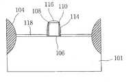
- With reference to FIG. 1,[0027]
device separators 104, or isolation structures, are formed on asemiconductor substrate 101 to define an active area, or active region, between theseparators 104. Preferably, thesemiconductor substrate 101 is composed of silicon. The device separators may be formed, for example, by any of the well-known techniques including the formation offield oxide structures 104 according to the local oxidation of silicon (LOCOS) process, and the shallow trench isolation (STI) method. - A[0028]
gate dielectric 106 is formed on the active region of thesemiconductor substrate 101, for example, by a deposit of a material selected from the group consisting of SiO2, SiON, SiN, A12O3, and mixtures thereof In one embodiment, the resultinggate dielectric 106 thus formed is 20 to 100 Å in thickness. - A conductive film for a gate electrode is then deposited on the active area of the[0029]
semiconductor substrate 101 on which thegate dielectric 106 is formed, and the resultingsemiconductor substrate 101 is patterned to form thegate electrode 108 structure on thesemiconductor substrate 101. In this regard, in one embodiment, the material of the conductive film is selected from the group consisting of poly-silicon (poly-Si), silicon-germanium (SiGe), and germanium (Ge), and other applicable conductive materials. Thegate electrode 108 is subjected to an oxidation process or a chemical vapor deposition (CVD) process to form afirst gate oxide 110 on lateral surfaces, or side walls, of thegate electrode 108. A dielectric layer, such as a nitride (e.g. SiN) layer, is then formed on thesemiconductor substrate 101 according to the CVD process, and the resultingsemiconductor substrate 101 is etched to form afirst gate spacer 114 on thefirst gate oxide 110. At this time, the gate dielectric layer, other than that portion covered by a lower portion of thefirst gate oxide 110 surrounding thegate electrode 108 and other than that portion positioned under thefirst gate electrode 108 is etched in an anisotropic etching procedure, while thesemiconductor substrate 101 is etched to form thefirst gate spacer 114. - After the formation of the[0030]
first gate spacer 114, a high-temperature hydrogen baking process using hydrogen gas is conducted so as to smoothly deposit a first epi-layer 118 on thesemiconductor substrate 101 in accordance with a selective epitaxial growth (SEG) process. At this time, it is preferable to conduct the hydrogen bake process at 800 to 900° C. under hydrogen atmosphere for one to five minutes. - Referring to FIG. 2, the SEG process is conducted in a low-pressure chemical vapor deposition (LPCVD) or a ultra-high vacuum chemical vapor deposition (UHV-CVD) procedure to form a[0031]
gate silicon 116 on thegate electrode 108 and to form the first epi-layer 118 between thefield oxide 104 and thefirst gate spacer 114. In this regard, the first epi-layer 118 is about 20 to 30% of the resulting elevated source/drain layer, in terms of thickness. Thegate silicon 116 is extended by the SEG process to form a poly-layer. - Turning to FIG. 3, a dopant is implanted in a portion of the[0032]
semiconductor substrate 101 under the first epi-layer 118 at a concentration of about 1014ions/cm2, for example BF2is ion-implanted at 3 keV in the case of PMOS (p-channel metal-oxide semiconductor) and As is ion-implanted at 10 keV in the case of NMOS (n-channel metal-oxide semiconductor) in thesemiconductor substrate 101 to form a source/drain extension layer 112 in thesemiconductor substrate 101. - As shown in FIG. 4, a[0033]
second gate oxide 130 is formed on thefirst gate spacer 114 in accordance with the CVD process. A dielectric, such as nitride (e.g. SiN), is then deposited on thesecond gate oxide 130 by the CVD process so as to construct asecond gate spacer 134. Subsequently, the resultingsemiconductor substrate 101 is etched to form thesecond gate spacer 134. At this time, it is preferable that a lateral thickness ratio of thefirst gate spacer 114 to thesecond gate spacer 134 is about 1:5. - Referring to FIG. 5, the SEG process is conducted, for example using an LPCVD or UHV-CVD procedure, to form a second epi-[0034]
layer 140 on thegate silicon 116 and the first epi-layer 118. In this regard, the second epi-layer 140 is about 70 to 80% of the resulting elevated source/drain layer, in terms of thickness. Accordingly, it is preferable that a thickness ratio of the first epi-layer 118 to the second epi-layer 140 is about 2:5. In the present invention, the thickness of the first epi-layer 118 is about 100 Å, and that of the second epi-layer 140 is about 250 Å. - The extended[0035]
gate silicon 116 is once again extended by the SEG process of FIG. 5. As a result, the width of the poly-layer positioned on the gate electrode is larger than the width of the gate. It is preferable that the poly-layer 116 positioned on thegate electrode 108 includes silicon or germanium. Accordingly, when the gate silicon is extended in this manner, the gate resistance is reduced, and the device junction leakage property is improved because, owing to the extension, the gate suicide is farther away from the junctions. - With reference to FIG. 6, the dopant is deeply ion-implanted into a portion of the[0036]
semiconductor substrate 101 positioned under the second epi-layer 140 to form deep source/drain regions 120 under the source/drain electrodes, and the resultingsemiconductor substrate 101 is annealed to activate the dopant ion-implanted in thesemiconductor substrate 101. - Additionally, when the first or second epi-[0037]
layer - Alternatively, when the first or second epi-[0038]
layer - On the other hand, when the first or second epi-[0039]
layer - Furthermore, when the first or second epi-[0040]
layer - Meanwhile, the dopant content in the first or second epi-[0041]
layer layer - As described above, the present invention provides a method of fabricating a MOS transistor with an elevated source/drain structure in accordance with a selective epitaxial growth (SEG) process, in which a source/drain extension junction is formed after an epi-layer is formed, thereby preventing the short channel effect which otherwise would have been caused by the diffusion of the source/drain junctions; leakage current is therefore reduced. Furthermore, the configuration and process of the present invention are advantageous in that the source/drain extension junctions are partially overlapped by a lower portion of the gate structure, because two lateral gate spacers are formed and two elevated source/drain layers are formed in accordance with the selective epitaxial growth process, thereby preventing the short channel effect and, at the same time, reducing sheet resistance of the source/drain layer and the gate layer.[0042]
- While this invention has been particularly shown and described with references to preferred embodiments thereof, it will be understood by those skilled in the art that various changes in form and details may be made herein without departing from the spirit and scope of the invention as defined by the appended claims.[0043]
Claims (37)
1. A method of fabricating a metal-oxide semiconductor (MOS) transistor having an elevated source/drain structure, comprising:
forming a gate dielectric on an active region of a semiconductor substrate and forming a gate electrode on the gate dielectric;
forming a first gate spacer on lateral side surfaces of the gate electrode;
forming a first epi-layer on the semiconductor substrate;
forming a second gate spacer on lateral side surfaces of the first gate spacer; and
forming a second epi-layer on the first epi-layer.
2. The method as set forth inclaim 1 , further comprising:
forming a first gate oxide on the lateral side surfaces of the gate electrode before the first gate spacer is formed; and
forming a second gate oxide on the lateral side surfaces of the first gate spacer before the second gate spacer is formed.
3. The method as set forth inclaim 1 , further comprising:
forming a first poly-layer on the gate electrode while the first epi-layer is formed; and
forming a second poly-layer on the first poly-layer while the second epi-layer is formed.
4. The method as set forth inclaim 1 , further comprising:
ion-implanting a dopant in the semiconductor substrate to form a source/drain extension layer after the first epi-layer is formed; and
ion-implanting a dopant in the semiconductor substrate to form a deep source/drain layer after the second epi-layer is formed.
5. The method as set forth inclaim 1 , wherein a thickness of the first epi-layer is about 20 to 30% of a combined thickness of an elevated source/drain layer formed by the first epi-layer and the second epi-layer.
6. The method as set forth inclaim 1 , wherein a thickness of the second epi-layer is about 70 to 80% of a combined thickness of an elevated source/drain layer formed by the first epi-layer and the second epi-layer.
7. The method as set forth inclaim 1 , wherein the second gate spacer is four to six times wider than the first gate spacer.
8. The method as set forth inclaim 1 , wherein at least one of the first epi-layer and second epi-layer comprises silicon.
9. The method as set forth inclaim 8 , wherein at least one of the first epi-layer and second epi-layer is grown in accordance with a low pressure chemical vapor deposition process.
10. The method as set forth inclaim 9 , wherein at least one of the first epi-layer and second epi-layer is formed using a source gas including dichlorosilane and HCl.
11. The method as set forth inclaim 9 , wherein the low pressure chemical vapor deposition process is conducted under 10 to 30 torr.
12. The method as set forth inclaim 8 , wherein at least one of the first epi-layer and second epi-layer is grown in accordance with an ultra-high vacuum chemical vapor deposition process.
13. The method as set forth inclaim 12 , wherein at least one of the first epi-layer and second epi-layer is formed using a source gas, including Si2H6.
14. The method as set forth inclaim 12 , wherein the ultra-high vacuum chemical vapor deposition process is conducted under 10−4to 10−5torr.
15. The method as set forth inclaim 8 , further comprising:
baking the semiconductor substrate or the first epi-layer at 800 to 900° C. under a hydrogen atmosphere for one to five minutes before the at least one of the first epi-layer and second epi-layer is formed.
16. The method as set forth inclaim 1 , wherein at least one of the first epi-layer and second epi-layer comprises silicon-germanium.
17. The method as set forth inclaim 16 , wherein at least one of the first epi-layer and second epi-layer is grown in accordance with a low pressure chemical vapor deposition process.
18. The method as set forth inclaim 17 , wherein at least one of the first epi-layer and second epi-layer is formed using a source gas, including dichlorosilane, HCl, and GeH4.
19. The method as set forth inclaim 17 , wherein the low pressure chemical vapor deposition process is conducted under 10 to 30 torr.
20. The method as set forth inclaim 16 , wherein at least one of the first epi-layer and second epi-layer is grown in accordance with a ultra-high vacuum chemical vapor deposition process.
21. The method as set forth inclaim 20 , wherein at least one of the first epi-layer and second epi-layer is formed using a source gas, including dichlorosilane, HCl, and GeH4.
22. The method as set forth inclaim 20 , wherein the ultra-high vacuum chemical vapor deposition process is conducted under 10−4to 10−5torr.
23. The method as set forth inclaim 16 , further comprising:
baking the semiconductor substrate or the first epi-layer at 800 to 900° C. under a hydrogen atmosphere for one to five minutes before the first epi-layer or second epi-layer is formed.
24. The method as set forth inclaim 1 , further comprising forming a source/drain layer by in-situ doping a dopant in at least one of the first epi-layer and second epi-layer during forming the first epi-layer or second epi-layer.
25. The method as set forth inclaim 1 , further comprising forming a source/drain layer by ion-implanting a dopant in at least one of the first epi-layer or second epi-layer during forming the first epi-layer or second epi-layer.
26. A metal-oxide semiconductor (MOS) transistor having an elevated source/drain structure, comprising:
a gate dielectric formed on an active region of a semiconductor substrate;
a gate electrode formed on the gate dielectric;
a first gate spacer formed on a lateral side surfaces of the gate electrode;
a first epi-layer formed on the semiconductor substrate;
a second gate spacer formed on lateral side surfaces of the first gate spacer; and
a second epi-layer formed on the first epi-layer.
27. The MOS transistor as set forth inclaim 26 , further comprising:
a first gate oxide between the gate electrode and the first gate spacer; and
a second gate oxide between the first gate spacer and the second gate spacer.
28. The MOS transistor as set forth inclaim 26 , further comprising a poly-layer on the gate electrode.
29. The MOS transistor as set forth inclaim 28 , wherein a width of the poly-layer on the gate electrode is wider than a width of the gate electrode.
30. The MOS transistor as set forth inclaim 28 , wherein the poly-layer on the gate electrode comprises silicon.
31. The MOS transistor as set forth inclaim 28 , wherein the poly-layer on the gate electrode comprises germanium.
32. The MOS transistor as set forth inclaim 26 , further comprising:
a source/drain extension layer formed by a dopant ion-implanting process, said source/drain extension layer being positioned under the first epi-layer and partially overlapped by a lower portion of the gate electrode; and
a deep source/drain layer formed by deeply ion-implanting a dopant in a portion of the semiconductor substrate positioned under the second epi-layer.
33. The MOS transistor as set forth inclaim 26 , wherein a thickness of the first epi-layer is about 20 to 30% of a combined thickness of an elevated source/drain layer formed by the first epi-layer and the second epi-layer.
34. The MOS transistor as set forth inclaim 26 , wherein a thickness of the second epi-layer is about 70 to 80% of a combined thickness of an elevated source/drain layer formed by the first epi-layer and the second epi-layer.
35. The MOS transistor as set forth inclaim 26 , wherein at least one of the first epi-layer and second epi-layer comprises silicon.
36. The MOS transistor as set forth inclaim 26 , wherein the second gate spacer is four to six times wider than the first gate spacer.
37. The MOS transistor as set forth inclaim 26 , wherein at least one of the first epi-layer and second epi-layer comprises silicon-germanium.
Priority Applications (1)
| Application Number | Priority Date | Filing Date | Title |
|---|---|---|---|
| US11/388,868US7368792B2 (en) | 2003-05-14 | 2006-03-24 | MOS transistor with elevated source/drain structure |
Applications Claiming Priority (2)
| Application Number | Priority Date | Filing Date | Title |
|---|---|---|---|
| KR1020030030614AKR100621546B1 (en) | 2003-05-14 | 2003-05-14 | Most transistors with elevated source / drain structure and manufacturing method thereof |
| KR03-30614 | 2003-05-14 |
Related Child Applications (1)
| Application Number | Title | Priority Date | Filing Date |
|---|---|---|---|
| US11/388,868DivisionUS7368792B2 (en) | 2003-05-14 | 2006-03-24 | MOS transistor with elevated source/drain structure |
Publications (2)
| Publication Number | Publication Date |
|---|---|
| US20040227164A1true US20040227164A1 (en) | 2004-11-18 |
| US7033895B2 US7033895B2 (en) | 2006-04-25 |
Family
ID=36695818
Family Applications (2)
| Application Number | Title | Priority Date | Filing Date |
|---|---|---|---|
| US10/823,420Expired - LifetimeUS7033895B2 (en) | 2003-05-14 | 2004-04-13 | Method of fabricating a MOS transistor with elevated source/drain structure using a selective epitaxial growth process |
| US11/388,868Expired - LifetimeUS7368792B2 (en) | 2003-05-14 | 2006-03-24 | MOS transistor with elevated source/drain structure |
Family Applications After (1)
| Application Number | Title | Priority Date | Filing Date |
|---|---|---|---|
| US11/388,868Expired - LifetimeUS7368792B2 (en) | 2003-05-14 | 2006-03-24 | MOS transistor with elevated source/drain structure |
Country Status (4)
| Country | Link |
|---|---|
| US (2) | US7033895B2 (en) |
| EP (2) | EP1478029B1 (en) |
| KR (1) | KR100621546B1 (en) |
| CN (1) | CN100456439C (en) |
Cited By (35)
| Publication number | Priority date | Publication date | Assignee | Title |
|---|---|---|---|---|
| US20070267691A1 (en)* | 2006-05-19 | 2007-11-22 | Promos Technologies Inc. | Metal oxide semiconductor transistor and fabrication method thereof |
| US20100151613A1 (en)* | 2007-05-29 | 2010-06-17 | Sony Corporation | Solid-state imaging device, method of manufacturing the same, and imaging apparatus |
| US20130082309A1 (en)* | 2011-10-04 | 2013-04-04 | Taiwan Semiconductor Manufacturing Company, Ltd. | Semiconductor device and fabrication method thereof |
| US8426284B2 (en) | 2011-05-11 | 2013-04-23 | United Microelectronics Corp. | Manufacturing method for semiconductor structure |
| US8431460B2 (en) | 2011-05-27 | 2013-04-30 | United Microelectronics Corp. | Method for fabricating semiconductor device |
| US8445363B2 (en) | 2011-04-21 | 2013-05-21 | United Microelectronics Corp. | Method of fabricating an epitaxial layer |
| US8466502B2 (en) | 2011-03-24 | 2013-06-18 | United Microelectronics Corp. | Metal-gate CMOS device |
| US8476169B2 (en) | 2011-10-17 | 2013-07-02 | United Microelectronics Corp. | Method of making strained silicon channel semiconductor structure |
| US8481391B2 (en) | 2011-05-18 | 2013-07-09 | United Microelectronics Corp. | Process for manufacturing stress-providing structure and semiconductor device with such stress-providing structure |
| US20130240999A1 (en)* | 2006-08-01 | 2013-09-19 | Nxp B.V. | Effecting selectivity of silicon or silicon-germanium deposition on a silicon or silicon-germanium substrate by doping |
| US8575043B2 (en) | 2011-07-26 | 2013-11-05 | United Microelectronics Corp. | Semiconductor device and manufacturing method thereof |
| US8647953B2 (en) | 2011-11-17 | 2014-02-11 | United Microelectronics Corp. | Method for fabricating first and second epitaxial cap layers |
| US8647941B2 (en) | 2011-08-17 | 2014-02-11 | United Microelectronics Corp. | Method of forming semiconductor device |
| US8664069B2 (en) | 2012-04-05 | 2014-03-04 | United Microelectronics Corp. | Semiconductor structure and process thereof |
| US8674433B2 (en) | 2011-08-24 | 2014-03-18 | United Microelectronics Corp. | Semiconductor process |
| US8691659B2 (en) | 2011-10-26 | 2014-04-08 | United Microelectronics Corp. | Method for forming void-free dielectric layer |
| US8709930B2 (en) | 2011-11-25 | 2014-04-29 | United Microelectronics Corp. | Semiconductor process |
| US8710632B2 (en) | 2012-09-07 | 2014-04-29 | United Microelectronics Corp. | Compound semiconductor epitaxial structure and method for fabricating the same |
| US8716750B2 (en) | 2011-07-25 | 2014-05-06 | United Microelectronics Corp. | Semiconductor device having epitaxial structures |
| US8754448B2 (en) | 2011-11-01 | 2014-06-17 | United Microelectronics Corp. | Semiconductor device having epitaxial layer |
| US8753902B1 (en) | 2013-03-13 | 2014-06-17 | United Microelectronics Corp. | Method of controlling etching process for forming epitaxial structure |
| US8765546B1 (en) | 2013-06-24 | 2014-07-01 | United Microelectronics Corp. | Method for fabricating fin-shaped field-effect transistor |
| US8796695B2 (en) | 2012-06-22 | 2014-08-05 | United Microelectronics Corp. | Multi-gate field-effect transistor and process thereof |
| US8835243B2 (en) | 2012-05-04 | 2014-09-16 | United Microelectronics Corp. | Semiconductor process |
| US8853060B1 (en) | 2013-05-27 | 2014-10-07 | United Microelectronics Corp. | Epitaxial process |
| US8866230B2 (en) | 2012-04-26 | 2014-10-21 | United Microelectronics Corp. | Semiconductor devices |
| US8895396B1 (en) | 2013-07-11 | 2014-11-25 | United Microelectronics Corp. | Epitaxial Process of forming stress inducing epitaxial layers in source and drain regions of PMOS and NMOS structures |
| US8951876B2 (en) | 2012-06-20 | 2015-02-10 | United Microelectronics Corp. | Semiconductor device and manufacturing method thereof |
| US8981487B2 (en) | 2013-07-31 | 2015-03-17 | United Microelectronics Corp. | Fin-shaped field-effect transistor (FinFET) |
| US9034705B2 (en) | 2013-03-26 | 2015-05-19 | United Microelectronics Corp. | Method of forming semiconductor device |
| US9064893B2 (en) | 2013-05-13 | 2015-06-23 | United Microelectronics Corp. | Gradient dopant of strained substrate manufacturing method of semiconductor device |
| US9076652B2 (en) | 2013-05-27 | 2015-07-07 | United Microelectronics Corp. | Semiconductor process for modifying shape of recess |
| US9117925B2 (en) | 2013-01-31 | 2015-08-25 | United Microelectronics Corp. | Epitaxial process |
| US9136348B2 (en) | 2012-03-12 | 2015-09-15 | United Microelectronics Corp. | Semiconductor structure and fabrication method thereof |
| US9202914B2 (en) | 2012-03-14 | 2015-12-01 | United Microelectronics Corporation | Semiconductor device and method for fabricating the same |
Families Citing this family (16)
| Publication number | Priority date | Publication date | Assignee | Title |
|---|---|---|---|---|
| EP2228931A3 (en)* | 2003-11-12 | 2010-11-17 | Interdigital Technology Corporation | System for application server autonomous access across different types of access technology networks |
| KR101146233B1 (en)* | 2005-06-30 | 2012-05-17 | 매그나칩 반도체 유한회사 | Method for fabricating semiconductor device |
| KR100632465B1 (en) | 2005-07-26 | 2006-10-09 | 삼성전자주식회사 | Semiconductor device and manufacturing method thereof |
| KR100721661B1 (en)* | 2005-08-26 | 2007-05-23 | 매그나칩 반도체 유한회사 | Image sensor and its manufacturing method |
| KR100748342B1 (en) | 2005-09-14 | 2007-08-09 | 매그나칩 반도체 유한회사 | Manufacturing Method of CMOS Image Sensor |
| KR100725455B1 (en) | 2005-12-12 | 2007-06-07 | 삼성전자주식회사 | Method of manufacturing a semiconductor memory device having an elevated source / drain |
| US7538387B2 (en)* | 2006-12-29 | 2009-05-26 | Taiwan Semiconductor Manufacturing Company, Ltd. | Stack SiGe for short channel improvement |
| US8202782B2 (en) | 2007-09-05 | 2012-06-19 | Nxp B.V. | Method of manufacturing transistor |
| US8420460B2 (en) | 2008-03-26 | 2013-04-16 | International Business Machines Corporation | Method, structure and design structure for customizing history effects of SOI circuits |
| US8410554B2 (en)* | 2008-03-26 | 2013-04-02 | International Business Machines Corporation | Method, structure and design structure for customizing history effects of SOI circuits |
| US20090278170A1 (en)* | 2008-05-07 | 2009-11-12 | Yun-Chi Yang | Semiconductor device and manufacturing method thereof |
| US8324059B2 (en) | 2011-04-25 | 2012-12-04 | United Microelectronics Corp. | Method of fabricating a semiconductor structure |
| CN102931235B (en)* | 2011-08-12 | 2016-02-17 | 中芯国际集成电路制造(上海)有限公司 | MOS transistor and manufacture method thereof |
| US9941388B2 (en)* | 2014-06-19 | 2018-04-10 | Globalfoundries Inc. | Method and structure for protecting gates during epitaxial growth |
| CN110491934A (en)* | 2019-08-29 | 2019-11-22 | 上海华力集成电路制造有限公司 | FDSOI-MOS transistor, circuit unit and its manufacturing method |
| US11935793B2 (en)* | 2020-05-29 | 2024-03-19 | Taiwan Semiconductor Manufacturing Co., Ltd. | Dual dopant source/drain regions and methods of forming same |
Citations (9)
| Publication number | Priority date | Publication date | Assignee | Title |
|---|---|---|---|---|
| US5012306A (en)* | 1989-09-22 | 1991-04-30 | Board Of Regents, The University Of Texas System | Hot-carrier suppressed sub-micron MISFET device |
| US6022771A (en)* | 1999-01-25 | 2000-02-08 | International Business Machines Corporation | Fabrication of semiconductor device having shallow junctions and sidewall spacers creating taper-shaped isolation where the source and drain regions meet the gate regions |
| US6187642B1 (en)* | 1999-06-15 | 2001-02-13 | Advanced Micro Devices Inc. | Method and apparatus for making mosfet's with elevated source/drain extensions |
| US6235568B1 (en)* | 1999-01-22 | 2001-05-22 | Intel Corporation | Semiconductor device having deposited silicon regions and a method of fabrication |
| US6277677B1 (en)* | 1999-04-12 | 2001-08-21 | Hyundai Electronics Industries Co., Ltd. | Method of manufacturing a semiconductor device |
| US20010034085A1 (en)* | 1999-03-16 | 2001-10-25 | Kabushiki Kaisha Toshiba | Method of manufacturing a semiconductor and semiconductor device |
| US6326664B1 (en)* | 1994-12-23 | 2001-12-04 | Intel Corporation | Transistor with ultra shallow tip and method of fabrication |
| US6445042B1 (en)* | 1999-06-15 | 2002-09-03 | Advanced Micro Devices, Inc. | Method and apparatus for making MOSFETs with elevated source/drain extensions |
| US6727543B2 (en)* | 2002-06-19 | 2004-04-27 | Yung-Chang Lin | Method for fabricating a memory structure having required scale spacers |
Family Cites Families (9)
| Publication number | Priority date | Publication date | Assignee | Title |
|---|---|---|---|---|
| US5093275A (en)* | 1989-09-22 | 1992-03-03 | The Board Of Regents, The University Of Texas System | Method for forming hot-carrier suppressed sub-micron MISFET device |
| US5168072A (en) | 1990-10-12 | 1992-12-01 | Texas Instruments Incorporated | Method of fabricating an high-performance insulated-gate field-effect transistor |
| US5539339A (en)* | 1994-06-15 | 1996-07-23 | U.S. Philips Corporation | Differential load stage with stepwise variable impedance, and clocked comparator comprising such a load stage |
| JP2848299B2 (en) | 1995-12-21 | 1999-01-20 | 日本電気株式会社 | Semiconductor device and manufacturing method thereof |
| KR100333727B1 (en)* | 1998-12-22 | 2002-06-20 | 박종섭 | Method for fabricating MOSFET with elevated source/drain structure |
| US5998248A (en)* | 1999-01-25 | 1999-12-07 | International Business Machines Corporation | Fabrication of semiconductor device having shallow junctions with tapered spacer in isolation region |
| JP2002026310A (en)* | 2000-06-30 | 2002-01-25 | Toshiba Corp | Semiconductor device and manufacturing method thereof |
| KR100374649B1 (en)* | 2001-08-04 | 2003-03-03 | Samsung Electronics Co Ltd | Structure of semiconductor device and manufacturing method thereof |
| US20030166323A1 (en) | 2002-03-01 | 2003-09-04 | Infineon Technologies North America Corp. | Raised extension structure for high performance cmos |
- 2003
- 2003-05-14KRKR1020030030614Apatent/KR100621546B1/ennot_activeExpired - Fee Related
- 2004
- 2004-04-13USUS10/823,420patent/US7033895B2/ennot_activeExpired - Lifetime
- 2004-04-21EPEP04009363.5Apatent/EP1478029B1/ennot_activeExpired - Lifetime
- 2004-04-21EPEP12194669Apatent/EP2565931A1/ennot_activeWithdrawn
- 2004-05-14CNCNB2004100433165Apatent/CN100456439C/ennot_activeExpired - Lifetime
- 2006
- 2006-03-24USUS11/388,868patent/US7368792B2/ennot_activeExpired - Lifetime
Patent Citations (9)
| Publication number | Priority date | Publication date | Assignee | Title |
|---|---|---|---|---|
| US5012306A (en)* | 1989-09-22 | 1991-04-30 | Board Of Regents, The University Of Texas System | Hot-carrier suppressed sub-micron MISFET device |
| US6326664B1 (en)* | 1994-12-23 | 2001-12-04 | Intel Corporation | Transistor with ultra shallow tip and method of fabrication |
| US6235568B1 (en)* | 1999-01-22 | 2001-05-22 | Intel Corporation | Semiconductor device having deposited silicon regions and a method of fabrication |
| US6022771A (en)* | 1999-01-25 | 2000-02-08 | International Business Machines Corporation | Fabrication of semiconductor device having shallow junctions and sidewall spacers creating taper-shaped isolation where the source and drain regions meet the gate regions |
| US20010034085A1 (en)* | 1999-03-16 | 2001-10-25 | Kabushiki Kaisha Toshiba | Method of manufacturing a semiconductor and semiconductor device |
| US6277677B1 (en)* | 1999-04-12 | 2001-08-21 | Hyundai Electronics Industries Co., Ltd. | Method of manufacturing a semiconductor device |
| US6187642B1 (en)* | 1999-06-15 | 2001-02-13 | Advanced Micro Devices Inc. | Method and apparatus for making mosfet's with elevated source/drain extensions |
| US6445042B1 (en)* | 1999-06-15 | 2002-09-03 | Advanced Micro Devices, Inc. | Method and apparatus for making MOSFETs with elevated source/drain extensions |
| US6727543B2 (en)* | 2002-06-19 | 2004-04-27 | Yung-Chang Lin | Method for fabricating a memory structure having required scale spacers |
Cited By (54)
| Publication number | Priority date | Publication date | Assignee | Title |
|---|---|---|---|---|
| US20070267691A1 (en)* | 2006-05-19 | 2007-11-22 | Promos Technologies Inc. | Metal oxide semiconductor transistor and fabrication method thereof |
| US7494865B2 (en)* | 2006-05-19 | 2009-02-24 | Promos Technologies Inc. | Fabrication method of metal oxide semiconductor transistor |
| US8790969B2 (en)* | 2006-08-01 | 2014-07-29 | Stmicroelectronics (Crolles 2) Sas | Effecting selectivity of silicon or silicon-germanium deposition on a silicon or silicon-germanium substrate by doping |
| US20130240999A1 (en)* | 2006-08-01 | 2013-09-19 | Nxp B.V. | Effecting selectivity of silicon or silicon-germanium deposition on a silicon or silicon-germanium substrate by doping |
| US20100151613A1 (en)* | 2007-05-29 | 2010-06-17 | Sony Corporation | Solid-state imaging device, method of manufacturing the same, and imaging apparatus |
| US20140008703A1 (en)* | 2007-05-29 | 2014-01-09 | Sony Corporation | Solid-state imaging device, manufacturing method thereof, and camera with alternately arranged pixel combinations |
| US8704276B2 (en) | 2007-05-29 | 2014-04-22 | Sony Corporation | Solid-state imaging device, method of manufacturing the same, and imaging apparatus |
| US8541255B2 (en)* | 2007-05-29 | 2013-09-24 | Sony Corporation | Solid-state imaging device, method of manufacturing the same, and imaging apparatus |
| US8592271B2 (en) | 2011-03-24 | 2013-11-26 | United Microelectronics Corp. | Metal-gate CMOS device and fabrication method thereof |
| US8466502B2 (en) | 2011-03-24 | 2013-06-18 | United Microelectronics Corp. | Metal-gate CMOS device |
| US8445363B2 (en) | 2011-04-21 | 2013-05-21 | United Microelectronics Corp. | Method of fabricating an epitaxial layer |
| US8426284B2 (en) | 2011-05-11 | 2013-04-23 | United Microelectronics Corp. | Manufacturing method for semiconductor structure |
| US8481391B2 (en) | 2011-05-18 | 2013-07-09 | United Microelectronics Corp. | Process for manufacturing stress-providing structure and semiconductor device with such stress-providing structure |
| US8431460B2 (en) | 2011-05-27 | 2013-04-30 | United Microelectronics Corp. | Method for fabricating semiconductor device |
| US8716750B2 (en) | 2011-07-25 | 2014-05-06 | United Microelectronics Corp. | Semiconductor device having epitaxial structures |
| US8575043B2 (en) | 2011-07-26 | 2013-11-05 | United Microelectronics Corp. | Semiconductor device and manufacturing method thereof |
| US8647941B2 (en) | 2011-08-17 | 2014-02-11 | United Microelectronics Corp. | Method of forming semiconductor device |
| US8674433B2 (en) | 2011-08-24 | 2014-03-18 | United Microelectronics Corp. | Semiconductor process |
| US10854748B2 (en) | 2011-10-04 | 2020-12-01 | Taiwan Semiconductor Manufacturing Company, Ltd. | Semiconductor device having first and second epitaxial materials |
| US9401426B2 (en) | 2011-10-04 | 2016-07-26 | Taiwan Semiconductor Manufacturing Company, Ltd. | Semiconductor device and fabrication method thereof |
| US8927374B2 (en)* | 2011-10-04 | 2015-01-06 | Taiwan Semiconductor Manufacturing Company, Ltd. | Semiconductor device and fabrication method thereof |
| US9842930B2 (en) | 2011-10-04 | 2017-12-12 | Taiwan Semiconductor Manufacturing Company, Ltd. | Semiconductor device and fabrication method thereof |
| US11257951B2 (en) | 2011-10-04 | 2022-02-22 | Taiwan Semiconductor Manufacturing Company, Ltd. | Method of making semiconductor device having first and second epitaxial materials |
| US20130082309A1 (en)* | 2011-10-04 | 2013-04-04 | Taiwan Semiconductor Manufacturing Company, Ltd. | Semiconductor device and fabrication method thereof |
| US8476169B2 (en) | 2011-10-17 | 2013-07-02 | United Microelectronics Corp. | Method of making strained silicon channel semiconductor structure |
| US8853740B2 (en) | 2011-10-17 | 2014-10-07 | United Microelectronics Corp. | Strained silicon channel semiconductor structure |
| US8691659B2 (en) | 2011-10-26 | 2014-04-08 | United Microelectronics Corp. | Method for forming void-free dielectric layer |
| US8754448B2 (en) | 2011-11-01 | 2014-06-17 | United Microelectronics Corp. | Semiconductor device having epitaxial layer |
| US8927376B2 (en) | 2011-11-01 | 2015-01-06 | United Microelectronics Corp. | Semiconductor device and method of forming epitaxial layer |
| US8647953B2 (en) | 2011-11-17 | 2014-02-11 | United Microelectronics Corp. | Method for fabricating first and second epitaxial cap layers |
| US8709930B2 (en) | 2011-11-25 | 2014-04-29 | United Microelectronics Corp. | Semiconductor process |
| US9312359B2 (en) | 2012-03-12 | 2016-04-12 | United Microelectronics Corp. | Semiconductor structure and fabrication method thereof |
| US9136348B2 (en) | 2012-03-12 | 2015-09-15 | United Microelectronics Corp. | Semiconductor structure and fabrication method thereof |
| US9443970B2 (en) | 2012-03-14 | 2016-09-13 | United Microelectronics Corporation | Semiconductor device with epitaxial structures and method for fabricating the same |
| US9202914B2 (en) | 2012-03-14 | 2015-12-01 | United Microelectronics Corporation | Semiconductor device and method for fabricating the same |
| US8884346B2 (en) | 2012-04-05 | 2014-11-11 | United Microelectronics Corp. | Semiconductor structure |
| US8664069B2 (en) | 2012-04-05 | 2014-03-04 | United Microelectronics Corp. | Semiconductor structure and process thereof |
| US8866230B2 (en) | 2012-04-26 | 2014-10-21 | United Microelectronics Corp. | Semiconductor devices |
| US8835243B2 (en) | 2012-05-04 | 2014-09-16 | United Microelectronics Corp. | Semiconductor process |
| US8951876B2 (en) | 2012-06-20 | 2015-02-10 | United Microelectronics Corp. | Semiconductor device and manufacturing method thereof |
| US9269811B2 (en) | 2012-06-20 | 2016-02-23 | United Microelectronics Corp. | Spacer scheme for semiconductor device |
| US8999793B2 (en) | 2012-06-22 | 2015-04-07 | United Microelectronics Corp. | Multi-gate field-effect transistor process |
| US8796695B2 (en) | 2012-06-22 | 2014-08-05 | United Microelectronics Corp. | Multi-gate field-effect transistor and process thereof |
| US8710632B2 (en) | 2012-09-07 | 2014-04-29 | United Microelectronics Corp. | Compound semiconductor epitaxial structure and method for fabricating the same |
| US9117925B2 (en) | 2013-01-31 | 2015-08-25 | United Microelectronics Corp. | Epitaxial process |
| US8753902B1 (en) | 2013-03-13 | 2014-06-17 | United Microelectronics Corp. | Method of controlling etching process for forming epitaxial structure |
| US9034705B2 (en) | 2013-03-26 | 2015-05-19 | United Microelectronics Corp. | Method of forming semiconductor device |
| US9064893B2 (en) | 2013-05-13 | 2015-06-23 | United Microelectronics Corp. | Gradient dopant of strained substrate manufacturing method of semiconductor device |
| US9263579B2 (en) | 2013-05-27 | 2016-02-16 | United Microelectronics Corp. | Semiconductor process for modifying shape of recess |
| US9076652B2 (en) | 2013-05-27 | 2015-07-07 | United Microelectronics Corp. | Semiconductor process for modifying shape of recess |
| US8853060B1 (en) | 2013-05-27 | 2014-10-07 | United Microelectronics Corp. | Epitaxial process |
| US8765546B1 (en) | 2013-06-24 | 2014-07-01 | United Microelectronics Corp. | Method for fabricating fin-shaped field-effect transistor |
| US8895396B1 (en) | 2013-07-11 | 2014-11-25 | United Microelectronics Corp. | Epitaxial Process of forming stress inducing epitaxial layers in source and drain regions of PMOS and NMOS structures |
| US8981487B2 (en) | 2013-07-31 | 2015-03-17 | United Microelectronics Corp. | Fin-shaped field-effect transistor (FinFET) |
Also Published As
| Publication number | Publication date |
|---|---|
| EP2565931A1 (en) | 2013-03-06 |
| KR100621546B1 (en) | 2006-09-13 |
| US20060163558A1 (en) | 2006-07-27 |
| EP1478029B1 (en) | 2014-04-16 |
| KR20040098302A (en) | 2004-11-20 |
| US7033895B2 (en) | 2006-04-25 |
| CN100456439C (en) | 2009-01-28 |
| EP1478029A1 (en) | 2004-11-17 |
| US7368792B2 (en) | 2008-05-06 |
| CN1551311A (en) | 2004-12-01 |
Similar Documents
| Publication | Publication Date | Title |
|---|---|---|
| US7033895B2 (en) | Method of fabricating a MOS transistor with elevated source/drain structure using a selective epitaxial growth process | |
| US8288825B2 (en) | Formation of raised source/drain structures in NFET with embedded SiGe in PFET | |
| US7226832B2 (en) | Complementary metal oxide semiconductor transistor technology using selective epitaxy of a strained silicon germanium layer | |
| US7452764B2 (en) | Gate-induced strain for MOS performance improvement | |
| US6916694B2 (en) | Strained silicon-channel MOSFET using a damascene gate process | |
| US8120065B2 (en) | Tensile strained NMOS transistor using group III-N source/drain regions | |
| US7700452B2 (en) | Strained channel transistor | |
| US7122435B2 (en) | Methods, systems and structures for forming improved transistors | |
| US7410875B2 (en) | Semiconductor structure and fabrication thereof | |
| US20080194070A1 (en) | Metal-oxide-semiconductor transistor device, manufacturing method thereof, and method of improving drain current thereof | |
| CN101632159A (en) | Stressed field effect transistor and method of making same | |
| US20110027954A1 (en) | Method to improve transistor tox using si recessing with no additional masking steps | |
| US20080132019A1 (en) | Short channel effect engineering in MOS device using epitaxially carbon-doped silicon | |
| US20100003799A1 (en) | Method for forming p-type lightly doped drain region using germanium pre-amorphous treatment | |
| US6815770B1 (en) | MOS transistor having reduced source/drain extension sheet resistance | |
| US7994591B2 (en) | Semiconductor device and method for manufacturing the same | |
| US7550356B2 (en) | Method of fabricating strained-silicon transistors | |
| US7892909B2 (en) | Polysilicon gate formation by in-situ doping | |
| US6905923B1 (en) | Offset spacer process for forming N-type transistors | |
| US20080194072A1 (en) | Polysilicon gate formation by in-situ doping | |
| US6184099B1 (en) | Low cost deep sub-micron CMOS process |
Legal Events
| Date | Code | Title | Description |
|---|---|---|---|
| AS | Assignment | Owner name:SAMSUNG ELECTRONICS CO., LTD., KOREA, REPUBLIC OF Free format text:ASSIGNMENT OF ASSIGNORS INTEREST;ASSIGNORS:LEE, SEUNG-HWAN;PARK, MOON-HAN;RHEE, HWA-SUNG;AND OTHERS;REEL/FRAME:015216/0142 Effective date:20040326 | |
| FEPP | Fee payment procedure | Free format text:PAYOR NUMBER ASSIGNED (ORIGINAL EVENT CODE: ASPN); ENTITY STATUS OF PATENT OWNER: LARGE ENTITY | |
| STCF | Information on status: patent grant | Free format text:PATENTED CASE | |
| CC | Certificate of correction | ||
| FEPP | Fee payment procedure | Free format text:PAYER NUMBER DE-ASSIGNED (ORIGINAL EVENT CODE: RMPN); ENTITY STATUS OF PATENT OWNER: LARGE ENTITY Free format text:PAYOR NUMBER ASSIGNED (ORIGINAL EVENT CODE: ASPN); ENTITY STATUS OF PATENT OWNER: LARGE ENTITY | |
| FPAY | Fee payment | Year of fee payment:4 | |
| FPAY | Fee payment | Year of fee payment:8 | |
| MAFP | Maintenance fee payment | Free format text:PAYMENT OF MAINTENANCE FEE, 12TH YEAR, LARGE ENTITY (ORIGINAL EVENT CODE: M1553) Year of fee payment:12 |